Embed Size (px)
Citation preview
Old Dominion University Old Dominion University
ODU Digital Commons ODU Digital Commons
Electrical & Computer Engineering Theses & Dissertations Electrical & Computer Engineering
Spring 2001
SPICE-Based Heat Transport Model for Non-Intrusive Thermal SPICE-Based Heat Transport Model for Non-Intrusive Thermal
Diagnostic Applications Diagnostic Applications
Michael Stelzer Old Dominion University
Follow this and additional works at: https://digitalcommons.odu.edu/ece_etds
Part of the Electrical and Computer Engineering Commons, and the Mechanical Engineering
Commons
Recommended Citation Recommended Citation Stelzer, Michael. "SPICE-Based Heat Transport Model for Non-Intrusive Thermal Diagnostic Applications" (2001). Master of Science (MS), Thesis, Electrical & Computer Engineering, Old Dominion University, DOI: 10.25777/xphr-5a82 https://digitalcommons.odu.edu/ece_etds/165
This Thesis is brought to you for free and open access by the Electrical & Computer Engineering at ODU Digital Commons. It has been accepted for inclusion in Electrical & Computer Engineering Theses & Dissertations by an authorized administrator of ODU Digital Commons. For more information, please contact [email protected].
SPICE BASED HEAT TRANSPORT MODEL FOR
NON-INTRUSIVE THERMAL DIAGONSTIC APPLICATIONS
B.S. in Electrical Engineering Technology DeVry Institute o f Technology, Columbus, Ohio.
A Thesis submitted to the faculty of Old Dominion University in Partial Fulfillment o f the
Requirement for the Degree of
MASTER OF SCIENCE
ELECTRICAL ENGINEERING
OLD DOMINION UNIVERSITY MAY 2001
byMichael Stelzer
Approved by:
Dr. Ravindra P. Joshi (Director)
Dr. Linda Vahala (Member)
£)r. Frederic McKenzie (Member)
Reproduced with permission of the copyright owner. Further reproduction prohibited without permission.
ABSTRACT
SPICE BASED HEAT TRANSPORT MODEL FOR NON-
INTRUSIVE THERMAL DIAGONSTIC APPLICATIONS
Michael Stelzer
Old Dominion University
Director: Dr. Ravindra P. Joshi
Nondestructive material testing and diagnostics play an important role in reliability
analysis, component wear-out testing, life-cycle estimates, and safety inspections. O f the
several techniques available for nondestructive inspections, thermal analysis has been
chosen to be the focus o f this thesis research. An equivalence between the system o f
equations for the heat flow problem, and the variables o f circuit theory suggests that an
electrical model can be constructed to represent the actual thermal system. This electrical
model is constructed based upon a finite difference discretization o f the heat flow
equation. Using these associations a basic one-dimensional electrical model has been
constructed and linked with a circuit simulator (such as SPICE) to simulate the transient,
steady state and ac heating scenarios o f a sample thermal system. The basic model has
been proven to accurately represent the thermal system. It has then been expanded to
include temperature dependence o f the conductivity parameter (with the aid of voltage
controlled resistors) and multidimensional heat flow by extending the one-dimensional
circuit along various directions. Finally, this SPICE-based model has been applied for
thermal analysis of samples containing surface material defects such as cracks. It is
shown that the model can adequately locate such cracks based upon the electro-thermal
Reproduced with permission of the copyright owner. Further reproduction prohibited without permission.
relationships between time delay and voltage (temperature) magnitudes. It would thus be
a useful simulation tool in the analysis o f defects and for investigating non-intrusive
thermal diagnostic response.
Reproduced with permission of the copyright owner. Further reproduction prohibited without permission.

ACKNOWLEDGEMENTS
I would like to thank Dr. Ravindra Joshi for his guidance and support as my
academic and thesis advisor. I would also like to take this opportunity to thank Dr. Linda
Vahala and Dr. Frederic McKenzie for their time and consideration in serving on my
thesis guidance committee. Finally, I want to thank Timothy Matich and Edward
Gossman for introducing me to computer office software.
Reproduced with permission of the copyright owner. Further reproduction prohibited without permission.
TABLE OF CONTENTS
LIST OF TABLES...................................................................................................................... viLIST OF FIGURES................................................................................................................... vii
Chapters
I. INTRODUCTION.....................................................................................................................1THERMAL ISSUES AND THEIR ROLE IN ENGINEERING............................... 1HEAT TRANSPORT SIMULATIONS AND THEIR ADVANTAGES................ 4REVIEW OF SCHEMES FOR THERMAL ANALYSES....................................... 6
Computer Aided Finite Difference Techniques..............................................6Computer Based Finite Element Techniques.................................................. 9The Transmission Line Matrix Method......................................................... 10Thermal Analysis Using The SPICE Circuit Simulator.............................. 13Analytical Techniques and Fourier Series Solutions....................................14
CURRENT RESEARCH OBJECTIVES...................................................................14THESIS OUTLINE........................................................................................................16
II. BACKGROUND REVIEW ON HEAT TRANSPORT...................................................19INTRODUCTION.........................................................................................................19HEAT TRANSFER MECHANISMS.........................................................................19THERMAL CONDUCTION.......................................................................................20
THE MODEL....................................................................................................21SECTIONAL ANALYSIS..............................................................................21
HEAT CONVECTION................................................................................................ 25HEAT RADIATION..................................................................................................... 31
ID. METHODOLOGY AND IMPLEMENTATION............................................................36INTRODUCTION........................................................................................................ 36ELECTRICAL ANALOG OF THE THERMAL SYSTEM................................... 37
THERMAL RESISTANCE............................................................................38CAPACITANCE............................................................................................. 39CURRENT SOURCES................................................................................... 40VOLTAGE SOURCE..................................................................................... 41
EQUIVALENT LUMPED ELEMENT CIRCUIT................................................... 41ONE-DIMENSIONAL EQUIVALENT ELECTRICALANALYSIS.......................................................................................................41ANALYTICAL SOLUTION FOR THE ONE-DIMENSIONALTHERMAL SYSTEM.................................................................................... 42TWO-DIMENSIONAL ANALYSIS.............................................................45THREE-DIMENSIONAL ANALYSIS.........................................................47
TEMPERATURE DEPENDANT FEATURES........................................................48SPICE-BASED IMPLEMENTATION OF NONUNIFORMCONDUCTIVITY........................................................................................................ 51SIMPLE TEST CASE FOR A VALIDITY CHECK............................................... 53
Reproduced with permission of the copyright owner. Further reproduction prohibited without permission.
V
INITIAL CONDITIONS................................................................................ 53HEATING TRANSIENT ANALYSIS..........................................................55STEADY-STATE CONDITIONS................................................................. 58COOLING TRANSIENT ANALYSIS..........................................................59FINAL STATE................................................................................................ 61
THE 20-NODE BAR................................................................................................... 61CONCLUSION ON SIMULATIN ACCURACY....................................................69TEMPERATURE DEPENDANT MODEL TRANSIENT ANALYSIS.............. 71
INITIAL STEADY-STATE CONDITION..................................................72HEATING TRANSIENT ANALYSIS......................................................... 72COOLING TRANSIENT ANALYSIS......................................................... 74FINAL STATE................................................................................................ 76
IV. RESULTS FOR THE THERMAL DIAGNOSTIC PROBLEM.................................. 77INTRODUCTION........................................................................................................77THERMAL DIAGNOSTICS - APPLICATIONS AND SCOPE..........................78RESULTS FOR A SINGLE PULSED INPUT........................................................ 81
ONE-DIMENSIONAL ANALYSIS.............................................................81TWO-DIMENSIONAL (2-D) ANALYSIS..................................................83THREE-DIMENSIONAL ANALYSIS........................................................ 88
RESULTS FOR MULTIPLE PULSED INPUTS.................................................... 88ONE-DIMENSIONAL ANALYSIS............................................................. 88TWO-DIMENSIONAL ANALYSIS.............................................................94THREE-DIMENSIONAL (3-D) ANALYSIS............................................. 99SIMULATING SURFACE CRACKS......................................................... 100THE DIFFERENTIAL THERMAL ANALYZER (DTA)SIMULATOR................................................................................................105
ERROR DETECTION USING THE DTA...............................................107COMMENTS AND DISCUSSION OF RESULTS..............................................I l l
V. CONCLUSIONS................................................................................................................113OVERVIEW................................................................................................................113SUMMARY.................................................................................................................114SCOPE FOR FUTURE WORK................................................................................121
REFERENCES........................................................................................................................ 123
Reproduced with permission of the copyright owner. Further reproduction prohibited without permission.
vi
LIST OF TABLES
Table Page
3-1 Equivalent Model Substitutions........................................................................................41
3-2 Accuracy as a function of sub-section size at steady state........................................... 62
4-1 Individual plane voltage nodes......................................................................................... 84
Reproduced with permission of the copyright owner. Further reproduction prohibited without permission.
LIST OF FIGURES
Figure Page
2-1: Shifting temperature references to calculate junction temperatures............................24
2-2: Electrical model for conduction heat transfer................................................................24
2-3: Analytical temperature profile......................................................................................... 27
2-4: Convection heat transfer...................................................................................................29
2-5: Electrical model for convection heat transfer.................................................................30
2-6: SPICE equivalent model for heat convection.................................................................30
2-7: Lambert’s cosine law.........................................................................................................32
2-8: Heat radiated from a surface............................................................................................ 32
2-9: Electrical model equivalent for heat absorbed/emitted.................................................33
2-10: Electrical model equivalent for radiated heat...............................................................35
3-1. Example one-dimensional electrical equivalent of the thermal model...................... 42
3-2: Electrical equivalent circuit for a two-dimensional sample......................................... 46
3-3. Creating a three-dimensional sample by stacking planes............................................. 47
3-4: Electrical schematic attachment for three-dimensional analysis................................. 48
3-5(a): Bar conductance as a function o f voltage................................................................ 49
3-5(b): Sub-section conductance as a function of voltage....................................................50
3-6: Nonlinear sub-section resistance....................................................................................52
3-7: Calculating capacitor voltages for the initial condition................................................54
3-8: Voltage nodes 1-5 for initial condition........................................................................... 54
3-9: Voltage nodes 6-10 for initial condition.........................................................................55
3-10: Calculating final capacitor voltages for the charging cycle.......................................56
Reproduced with permission of the copyright owner. Further reproduction prohibited without permission.
v iii
3-11: Voltage nodes 1-5 for heating transient........................................................................ 57
3-12: Voltage nodes 6-10 for heating transient...................................................................... 57
3-13: Steady-state temperatures for nodes 1-5....................................................................... 58
3-14: Steady-state temperatures for nodes 6-10..................................................................... 59
3-15: Calculating final capacitor voltages for discharge cycle.......................................... 60
3-16: Cooling transients for nodes 1-5.................................................................................... 60
3-17: Cooling transients for nodes 6-10.................................................................................. 61
3-18: Voltage nodes 1 and 2 charging transients................................................................... 63
3-19: Voltage nodes 3 and 4 charging transients................................................................... 64
3-20: Voltage nodes 5 and 6 charging transients................................................................... 64
3-21: Voltage nodes 7 and 8 charging transients................................................................... 65
3-22: Voltage nodes 9 and 10 charging transients................................................................. 65
3-23: Voltage nodes 11 & 12 charging transients.................................................................. 66
3-24: Voltage nodes 13 & 14 charging transients.................................................................. 66
3-25: Voltage nodes 15 and 16 charging transients...............................................................67
3-26: Voltage nodes 17 and 18 charging transients...............................................................67
3-27: Voltage nodes 19 and 20 charging transients...............................................................68
3-28: Voltage nodes 1 and 2 discharge transients.................................................................. 68
3-29: Voltage nodes 19 and 20 discharge transients..............................................................69
3-30: Distribution function for reliability o f a 20-node m odel.......................................... 70
3-31: Distribution function for reliability o f a 10-node m odel..........................................71
3-32: Initial state voltages for the variable thermal conductivity model............................72
3-33: Variable thermal conductivity heating transients........................................................ 73
Reproduced with permission of the copyright owner. Further reproduction prohibited without permission.
3-34: Heating transient behavior comparison between models........................................... 73
3-35: Variable thermal conductivity cooling transients........................................................ 75
3-36: Cooling Transient behavior comparison between models..........................................75
4-1: Voltage-controlled heating source................................................................................... 82
4-2: Transient behavior o f a heating pulse directed at node 5 ............................................. 83
4-3: Separating the two-dimensional sample into individual sections................................ 83
4-4: Transient response o f nodes 1, 5, and 9 with stationary laser on section 5................ 85
4-5: Transient response o f nodes 2, 6, and 10 with stationary laser on section 5.............85
4-6: Transient response o f nodes 3, 7, and 11 with stationary laser on section 5.............86
4-7: Transient response o f nodes 4, 8, and 12 with stationary laser on section 5.............86
4-8: Transient response o f simulated cyclic heat pulse directed at node 5.........................89
4-9: Transient voltage o f node 1 for multiple current pulses at node 5 .............................. 89
4-10: Transient voltage o f node 1 for a constant current pulse at node 5 .......................... 90
4-11: Transient behavior o f nodes 1-5 for the traveling laser analysis............................... 92
4-12: Transient behavior o f nodes 6-10 for the traveling laser analysis.............................93
4-13: Transient behavior o f nodes 11-15 for the traveling laser analysis...........................93
4-14: Transient behavior o f nodes 16-20 for the traveling laser analysis...........................94
4-15: Voltage node 1 for two-dimensional simulations........................................................ 96
4-16: Voltage node 2 for two-dimensional simulation testing............................................. 97
4-17: Voltage node 4 for two-dimensional simulations........................................................ 97
4-18: Voltage node 11 for two-dimensional simulations......................................................98
4-19: Voltage node 12 for two-dimensional simulation testing...........................................98
4-20: Temperature profile o f node 1 for a three-dimensional sample................................ 99
Reproduced with permission of the copyright owner. Further reproduction prohibited without permission.
X
4-21: Electrical equivalent model o f a 0.7m square sample of silicon...............................100
4-22: Simulated heat pulse upon a cracked two-dimensional sample................................ 101
4-23: Node 44 voltage comparisons for a pure and a cracked surface..............................102
4-24: Node 52 voltage comparisons for a pure and a cracked surface.............................103
4-25: Voltage (temperature) response at nodes 34 and 36 for the simulated crack 104
4-26: Error signal at node 44 for the cracked surface example......................................... 107
4-27: Error signal of difference thermal analyzer simulator for an impure sample
(A )................................................................................................................................ 108
(B )................................................................................................................................ 109
(C )................................................................................................................................ 109
(D )................................................................................................................................ 110
(E )................................................................................................................................ 110
Reproduced with permission of the copyright owner. Further reproduction prohibited without permission.
1
CHAPTER 1
INTRODUCTION
1.1 THERMAL ISSUES AND THEIR ROLE IN ENGINEERING
Heat and thermal conduction play an important role consideration in several
engineering fields. The production o f heat is often a desirable product, such as in the
case o f welding, to produce energy such as the result o f fuel combustion, to drive
chemical reactions and affect their kinetics, and so on. At other times, it exists as an
undesirable by-product, such as in friction, power dissipation in electrical components,
and material property alterations. Thermal transport can similarly be beneficial in
applications such as forced cooling to prevent over-heating, to contain thermal
breakdown in semiconductor electronics, or to supply directed energy from a supply
source to a receiving element. For such purposes, heat is usually removed from the
system through an air or fluid cooling system. An example o f a fluid cooling system will
be presented in the heat convection section o f this text. Transport can also be detrimental
in that it leads to losses through undesirable thermal leakage and reduces the efficiency o f
thermal systems.
Heat induced by friction occurs when two objects in contact rub together. The
continuous rubbing of the materials creates a heat build up at the area of contact. When
an electrical current experiences a resistance, energy is lost in the form of heat. This heat
is usually radiated from the component directly or is transferred via conduction to an
attached heat sink. The heat sink absorbs a great portion o f the heat and transfers it to its
surroundings through radiation. Such transfer is necessary to curtail excessive heating
T he journal model for this work is the IF.F.F. inurnal
Reproduced with permission of the copyright owner. Further reproduction prohibited without permission.
2
and damage in the electrical circuit. Conduction and radiation heat transfer mechanisms
will also be modeled in this text.
The heating and/or thermal transport o f materials is characterized by a number of
important parameters. These values dictate the thermal behavior and properties of the
material. A property o f utmost importance is a material's thermal expansion coefficient,
which quantifies material expands or contraction with changes in temperature. Serious
problems can result by not giving due consideration to this property. For example, if two
materials of vastly different thermal expansion coefficients were joined together and
heated, a large stress possibly leading to buckling or breakage at the junction can result
due to unequal expansions o f the two constituent materials. Another is the thermal
conductivity coefficient, which is the measure of a material’s ability to transport heat
through conduction. This property is o f utmost important in devising thermal sinks and
heat exchangers, or to evaluate thermal losses of high-temperature environments and
chambers. As discussed later in this thesis, the thermal conductivity can itself depend on
the local temperature since the ability to carry heat is impeded by “phonon scattering” at
high temperatures.
In the context o f electrical engineering, the self-heating o f electronic devices and
thermal management issues have begun to take on increasing importance in integrated
circuit technology for a variety o f reasons. Device down scaling, functional integration,
and increases in the on-chip density naturally give rise to higher energy generation. The
need to develop reliable active devices for a variety of specific high-power, high-voltage
applications has also enhanced the interest in thermal analysis and heat management
issues. The applications can range from high power RF generation, solid-state broadband
Reproduced with permission of the copyright owner. Further reproduction prohibited without permission.
3
amplifiers for microwave communications including mobile phones, phased array radars,
and high voltage semiconductor switches for power factor control in transmission load
networks. The thermal problem is compounded by the need for high-speed electronics,
which invariably leads to GaAs as the material of choice. Unfortunately, the thermal
conductivity of GaAs (~ 0.46 W/K/cm) is an order of magnitude smaller than SiC, and is
lower by factors of 5 and 3, respectively, as compared to GaN and Si. It, therefore,
becomes more difficult to conduct away the heat from the active regions o f high-power,
high-speed GaAs circuits. As a consequence, internal temperature increases need to be
taken into account for all device optimization and design procedures.
Temperature increases produced by the internal heat generation affect several
parameters of electronic devices that collectively alter the overall response
characteristics. Fundamentally, the increased temperature has two main effects: (a) It
alters the carrier transport properties by modifying the carrier-phonon interactions, and
(b) it leads to an increase in the vibrational kinetic energies of the lattice atoms. The
effects on the electronic sub-system tend to reduce mobilities, carrier drift velocities, and
the overshoot characteristics. Other effects, often associated with the velocity reductions,
typically include reductions in the ac gain, lower transconductances in FET structures,
reductions in the cut-off frequency arising from increased transit times, decreases in the
characteristic breakdown voltage, increased leakage currents, higher shot-noise, larger
channel and series resistances which adversely affect the “RC” time constants, and
enhanced carrier emission from traps and defects. Increases in the atomic vibrational
energy lead to several consequences as well, some of which can be detrimental for the
stability and reliability o f the overall circuits. For example, higher atomic kinetic energies
Reproduced with permission of the copyright owner. Further reproduction prohibited without permission.
4
can enhance electromigration, facilitate the propagation o f defects and dislocations, and
cause the build up o f internal stresses and strains. In a perfect lattice containing no
imperfections, the temperature rise would not have as dramatic an effect, since the
internal symmetry would help in maintaining a balance between the inter-atomic forces.
If anything, the lower electron mobility would help reduce the “electron-wind”
contributions to electromigration. However, in the presence of defects or asymmetries
(including those at the metallization-semiconductor boundaries), increased temperatures
make it easier for atoms to hop over localized potential minima and migrate within the
lattice. Macroscopically, such atomic movement is characterized in terms o f activation
energy and the migration rate is typically expressed by an Arrhenium-type formula. The
resulting effects, such as defect propagation and internal stress, can in turn influence the
trapping-detrapping characteristics. This can potentially lead to instability either by
enhancing the internal electric fields through localized space charge formation, or by
providing a source of recombination heating which could then possibly lead to a positive
feedback action.
1.2 HEAT TRANSPORT SIMULATIONS AND THEIR ADVANTAGES
Computer simulations provide a method to study the response and behavior o f
real world systems through numerical evaluations based on software that is designed to
mimic the system’s operational behavior or characteristics. There are several advantages
o f undertaking such simulation studies. An important advantage is that simulations
provide the ability to deal with very complicated models and systems. Next, the
development of graphical user interfaces has made it possible to visualize the results,
Reproduced with permission of the copyright owner. Further reproduction prohibited without permission.
5
often in real time. The visualization helps in gaining insights into the phenomena of
interest and its dynamic evolution. The computational approaches also provide a cost-
effective tool for the study and analysis without the need for costly equipment or
experimental facilities. Furthermore, a large number o f scenarios and test cases can
easily and quickly be analyzed. In this thesis, computer simulations will be employed to
gauge an understanding of thermal transport and heat flow, both under transient and
steady state conditions. An electrical analogue to the thermal system will be constructed
for improved efficiency and computational speed. The advantage of setting up an
electrical equivalent to the thermal system will be that all the electrical circuit simulation
tools currently available will easily be brought to bear for the thermal problems.
In general, simulation uses methods and applications to mimic the behavior of
real systems. A system is usually studied to measure its performance, improve its
operation, or design it if it doesn't already exist. It might be possible to experiment with
the actual system to observe its response to parameter changes introduced by the analyst.
However, in many cases, it may be too difficult, costly, or dangerous to experiment on
the actual system. It is these situations in which it would prove beneficial to construct a
model for studying the system. The model allows the analyst to experiment with a
representation o f the system and produce safe and cost effective results.
In general, simulation models are generally classified into three categories: (i)
Static vs. Dynamic: A static model is time independent, but a dynamic model uses time
as a parameter. Most operational models are dynamic, (ii) Continuous vs. Discrete:
Continuous systems change continuously over time. A discrete model has change
occurring only at sets of distinct points in time, (iii) Deterministic vs. Stochastic: Models
Reproduced with permission of the copyright owner. Further reproduction prohibited without permission.
6
that use no random inputs are said to be deterministic. Stochastic models, however,
operate with random inputs and produce uncertain results. The heat transfer mechanism
models may be classified as static (since the results are not time dependant), discrete
(since the results do not vary over the simulation), and deterministic (since no random
inputs are considered).
1.3 REVIEW OF SCHEMES FOR THERMAL ANALYSES
Thermal modeling is not a new problem area, and an abundant literature exists on
the subject [for example, 1-11]. It is perhaps instructive to start with a summarizing
survey o f the various contributions in this field. Quite generally, there appear to be five
main techniques for analyzing the self-heating problems. These are listed below, with
brief discussions pertaining to their applicability, merits, and relative disadvantages.
These theoretical approaches are a good starting point for selecting an appropriate
procedure for the thermal analysis of electronic devices.
1.3.1 Computer Aided Finite Difference Techniques
Heat flow is assumed to be adequately represented by a non-linear diffusion
equation in accordance to Fick’s law. This inherently assumes an internal quasi
equilibrium between the various phonon modes, and is clearly applicable over
dimensions exceeding the thermal mean-free path. For simplicity, the finite difference
scheme will be discussed only for the one-dimensional (ID) case, though it can easily be
generalized to three dimensions. The 1D heat flow equation is given as:
Reproduced with permission of the copyright owner. Further reproduction prohibited without permission.
7
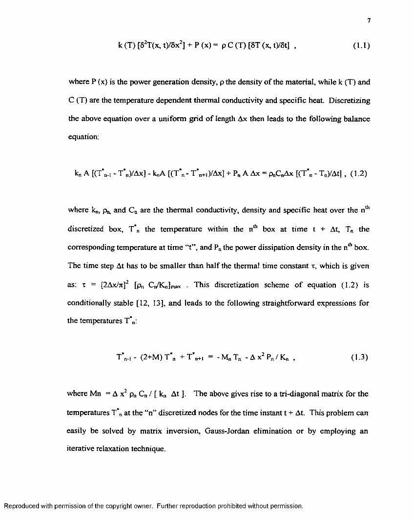
k(T) [82T(x,t)/8x2] + P ( x ) = p C ( T ) [8T(x,t)/St] , (1.1)
where P (x) is the power generation density, p the density o f the material, while k (T) and
C (T) are the temperature dependent thermal conductivity and specific heat. Discretizing
the above equation over a uniform grid o f length Ax then leads to the following balance
equation:
kn A [(T*n.i - T*n)/Ax] - knA [(T*n- T*n+i)/Ax] + Pn A Ax = pnCnAx [(T*n - Tn)/At] , (1.2)
where kn, and Q, are the thermal conductivity, density and specific heat over the n*
discretized box, T*n the temperature within the n* box at time t + At, Tn the
corresponding temperature at time “t”, and Pn the power dissipation density in the n1*1 box.
The time step At has to be smaller than half the thermal time constant t, which is given
as: x = [2Ax/7t]2 [p„ Cn/K n]niax • This discretization scheme o f equation (1.2) is
conditionally stable [12, 13], and leads to the following straightforward expressions for
the temperatures T*n:
TV! - (2+M) T*n + T V . = - Mn T„ - A x2 Pn / Kn , (1.3)
where Mn = A x2 p„ Cn / [ k„ At ]. The above gives rise to a tri-diagonal matrix for the
temperatures T*n at the “n” discretized nodes for the time instant t + At. This problem can
easily be solved by matrix inversion, Gauss-Jordan elimination or by employing an
iterative relaxation technique.
Reproduced with permission of the copyright owner. Further reproduction prohibited without permission.
8
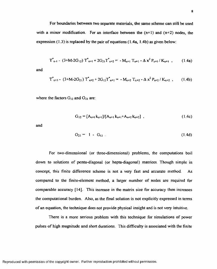
For boundaries between two separate materials, the same scheme can still be used
with a minor modification. For an interface between the (n+1) and (n+2) nodes, the
expression (1.3) is replaced by the pair o f equations (1.4a, 1.4b) as given below:
T n-i - (3+M-2Gi2) T n+i + 2G2iT*n+2 = - Mn+i Tn+i - A x2 P„+i / K„+i , (1.4a)
and
T n+3 - (3+M-2G2l) T n+2 + 2 G 12T n+l = “ Mn+2 Tn+2 - A x 2 Pn+2 / Kn+2 , (1.4b)
where the factors Gi2 and G 21 are:
G 12 [A.n+l kn+,]/[A„+, kn+l+An+2 kn+2 ] , (1.4c)
and
G21 = 1 - G , 2 ■ (1.4d)
For two-dimensional (or three-dimensional) problems, the computations boil
down to solutions of penta-diagonal (or hepta-diagonal) matrices. Though simple in
concept, this finite difference scheme is not a very fast and accurate method. As
compared to the finite-element method, a larger number o f nodes are required for
comparable accuracy [14], This increase in the matrix size for accuracy then increases
the computational burden. Also, as the final solution is not explicitly expressed in terms
o f an equation, the technique does not provide physical insight and is not very intuitive.
There is a more serious problem with this technique for simulations of power
pulses o f high magnitude and short durations. This difficulty is associated with the finite
Reproduced with permission of the copyright owner. Further reproduction prohibited without permission.
9
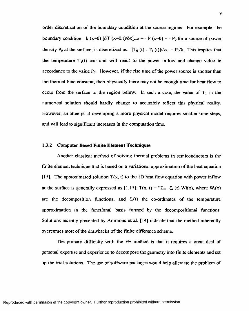
order discretization o f the boundary condition at the source regions. For example, the
boundary condition: k (x=0) [8T (x=0,t)/8x]x=o = - P (x=0) = - P0 for a source o f power
density P0 at the surface, is discretized as: [T0 (t) - Ti (t)]/Ax = Po/k. This implies that
the temperature Ti(t) can and will react to the power inflow and change value in
accordance to the value Po- However, if the rise time of the power source is shorter than
the thermal time constant, then physically there may not be enough time for heat flow to
occur from the surface to the region below. In such a case, the value o f Ti in the
numerical solution should hardly change to accurately reflect this physical reality.
However, an attempt at developing a more physical model requires smaller time steps,
and will lead to significant increases in the computation time.
1.3.2 Computer Based Finite Element Techniques
Another classical method o f solving thermal problems in semiconductors is the
finite element technique that is based on a variational approximation of the heat equation
[15]. The approximated solution T(x, t) to the ID heat flow equation with power inflow
at the surface is generally expressed as [1.15]: T(x, t) = mI,=i Q (t) Wi(x), where Wi(x)
are the decomposition functions, and £i(t) the co-ordinates of the temperature
approximation in the functional basis formed by the decompositional functions.
Solutions recently presented by Ammous et al. [14] indicate that the method inherently
overcomes most of the drawbacks o f the finite difference scheme.
The primary difficulty with the FE method is that it requires a great deal of
personal expertise and experience to decompose the geometry into finite elements and set
up the trial solutions. The use o f software packages would help alleviate the problem of
Reproduced with permission of the copyright owner. Further reproduction prohibited without permission.
10
this complicated and cumbersome technique. However, the method is not very
transparent, and does not lend itself to simple predictions o f scaling behavior. It could be
pursued if rigorous solutions to complicated geometric structures are desired. However,
for simple geometries, and as a quick design aid, some o f the analytical techniques
discussed later would be far more efficient.
1.3.3 The Transmission Line Matrix Method
The transmission line matrix (TLM) approach was first proposed by Johns [15]
and Lohse et al. [16] as an alternative for overcoming the shortcomings o f the finite
difference (FD) scheme. As discussed above, stability of the FD scheme requires that
the time step be less than half the thermal time constant. This can potentially result in
excessively long computational times or increases in the matrix storage requirements.
The TLM method, on the other hand, which relies on an equivalent RC transmission line
model, proves to be conditionally stable. Its main utility lies in the time dependent
domain o f heat flow analysis.
The TLM method was originally introduced to solve Maxwell’s equations, and
problems in the field o f electromagnetics and transmission lines [17,18], Its application
to thermal flow analysis stems from the fact that the form o f the wave equations of
electromagnetics and the transmission line expressions, both reduce to the heat diffusion
equation as the permittivity (or distributed inductance) become vanishingly small. This
correspondence between the electromagnetic and the thermal systems sets up an
equivalence between the voltages of transmission line theory and the temperature at an
internal node of the discretized semiconductor space. A discretized segment of the
Reproduced with permission of the copyright owner. Further reproduction prohibited without permission.
11
semiconductor material can then be represented in terms o f a differential element of a
transmission-line circuit. The resistance “Rtran” and capacitance “Ctnm” associated with
such an analogous transmission line model are then given as: Rtnm = Ax /[k A] and Ctran
= C p A Ax . The parameters k, C, and p are the thermal conductivity, specific heat, and
material density parameters, respectively. As a result, the issue of determining the heat
flow problem is transformed to an equivalent problem o f evaluating the time dependent
propagation o f voltage waveforms across the nodes o f a distributed transmission line
network. Since the equivalent network problem has only capacitors and resistors, it
represents a lossy system and is inherently stable. It thus ensures that any spurious
oscillations arising in this passive-network would quickly die away.
The TLM method provides an exact time-domain solution for the network by
considering the propagation o f delta pulses from the various source nodes. The source
nodes represent regions of actual power dissipation within the physical semiconductor
device. The essence o f the technique is to launch pulses from every source node and
propagate them down the elemental transmission line segments in all directions. After
propagating down a differential transmission line segment, the voltage pulses scatter and
are reflected. The time delays between all adjacent transmission line segments are set
equal, so that pulses arrive at all successive scattering zones simultaneously. In a sense,
the cumulative addition o f the voltage at each node following collective propagation and
scattering is paramount to a discretization o f Huygen’s principle. Secondary sources are
thus continually created at every time step as the wave interacts with successive
transmission line segments. The temporal development o f voltage in response to the
Reproduced with permission of the copyright owner. Further reproduction prohibited without permission.
12
initial set o f pulses then yields the equivalent temperature as a function o f position and
time.
The obvious advantage o f the TLM technique is the ease with which even the
most complicated geometric structures can be analyzed. There are no convergence or
stability problems. Also, a large amount o f information is made available by the TLM
approach. For example, the technique can yield the impulse response for a given
semiconductor structure. This can, in principle, allow for the computation o f the time-
dependent response o f the system to any excitation provided the system was linear.
Furthermore, the characteristics o f the dominant and higher order modes can be assessed
through a Fourier transform.
It is also important to state some of the drawbacks and potential sources of error
in applying the TLM method for thermal analysis. First, the technique requires that all
pulses propagating through the various transmission line segments arrive with perfect
synchronization. This implies that the thermal velocity is constant and uniform. In
practice, this would be difficult to achieve due to internal inhomogeneities, defects, and
temperature dependent material characteristics. Sloping boundaries would cause mis
alignments between the physical geometry and the simulated elemental regions leading to
timing errors. The temperature dependence of the material parameters that would
become especially important at the higher power dissipation levels would work to
invalidate the premise o f system linearity. This would bring into question the
applicability of the Fourier transform. Apart from the velocity errors, timing offsets, and
misalignment effects, truncation of the impulse response to a finite time duration would
also contribute to the errors. This effectively would lead to the Gibb’s phenomena. In
Reproduced with permission of the copyright owner. Further reproduction prohibited without permission.
13
view o f the above problems, the TLM is perhaps not very well suited for steady state
thermal analysis. It would best be used for simulations o f transient response, especially
for fast rising input pulses.
1.3.4 Thermal Analysis Using The SPICE Circuit Simulator
The equivalence between the thermal system o f equations and the variables of
circuit theory immediately suggests the use o f circuit simulators for the solution o f the
thermal problem. Based on a finite difference discretization o f the heat flow equation, an
equivalence between the following variables can be shown to result. Details of this are
discussed in Chapter 3.
As a result, a differential element o f volume within the semiconductor material
denoting a unit cell for the thermal problem may be presented in terms of an equivalent
electrical building block. This repetitive block would consist o f two serial resistors with
a parallel combination of a current source and a capacitor connected between them.
Obviously, for 2D or 3D analysis, one would have four- or six- resistors, respectively.
These building blocks would be interconnected to yield the volume o f the entire structure.
This equivalent electrical network could be solved for a given set o f current excitations,
using the commercially available SPICE simulator yielding all node voltages as a
function of time. Since SPICE programs are available, and are capable of handling a
large number of nodes, the thermal problem could be solved exactly.
Such equivalent electrical circuit simulations have been used for thermal analysis
[19, 20]. This approach can easily be generalized to include the temperature dependence
o f the thermal conductivity and specific heat by employing voltage controlled resistor and
Reproduced with permission of the copyright owner. Further reproduction prohibited without permission.
14
capacitor elements. Since voltage controlled elements are available within the SPICE
simulator, this extension should be trivial. The added advantage is that in addition to
time-domain analysis, the technique would easily furnish the frequency response
characteristics based on the built-in capability of the SPICE simulation tool.
13.5 Analytical Techniques and Fourier Series Solutions
This final class o f techniques is the least intensive computationally, and provides
closed form expressions for the internal device temperature. Quantities o f interest such
as the thermal resistance and peak surface temperature can easily be obtained. As such,
these methods appear to be best suited for quick device optimization or to ascertain the
thermal implications for competing layout schemes. Most o f the methods are intended
for analysis under steady state operating conditions.
1.4 CURRENT RESEARCH OBJECTIVES
The primaiy goal of this study is to analyze the problem o f heat flow and thermal
transport in solids through numerical simulations. There are a number o f numerical
modeling approaches to this problem based on the thermal equations. However, multi
purpose software packages and simulation tools for a variety o f operating conditions are
not easily available for the thermal problem. Simulators of electrical circuits, on the
other hand, are widely available and capable of performing dc, transient, and ac analysis.
The SPICE tool is one example with which all electrical engineers have a great deal of
familiarity. Consequently, one o f the primary objectives o f this research was to explore
Reproduced with permission of the copyright owner. Further reproduction prohibited without permission.
15
the feasibility o f utilizing such electrical circuit simulators for the solution of thermal
problems by establishing electrical analogues.
The focused objectives were the following: (1) Determine whether electrical
analogues could be constructed to represent both the transient and steady-state conditions
o f heat flow in solids. It was necessary and important to have a one-to-one
correspondence between the variables o f the thermal and electrical systems. (2) Ascertain
the equivalent electrical circuit elements (such as capacitors and conductors) required for
such a task. (3) Incorporate temperature dependence o f parameters such as the thermal
conductivity. (4) Demonstrate the validity of such a SPICE-based equivalent electrical
simulator for heat flow problems through careful comparisons.
The overall, long-term objective o f developing an alternate SPICE-based approach
is to be able to carry out steady-state, transient, and ffequency-response analysis o f both
pure (i.e., defect-free), and defective solids. The application to fatigue and defect
analysis from such simulations would be very important and useful for non-destructive
evaluation (NDE) and testing purposes. Laser-based spanning of samples is currently
being pursued as a superior fast, jitter-free technique for such NDE activity. It also has
the advantage of good spatial resolution. From this NDE standpoint, it is important for
this thesis work to also successfully carry out the following tasks, (a) To demonstrate
that clear differences exist in the results o f simulated heat flow between pure samples and
those containing defects and/or cracks, (b) Identify the parameters that can best carry
information on the defects. These are likely to be time-delays or magnitudes of the local
temperature in response to a laser-generated heat span, (c) Show at least one simple test
example of a SPICE-based method for irrefutable demonstration, (d) Eventually, based
Reproduced with permission of the copyright owner. Further reproduction prohibited without permission.
16
on the success of the results obtained in this research, more detailed analysis could be
developed for a more comprehensive and quantitative analysis. Recommendations and
suggestions on enhancing the applicability o f this mathematical model could also be
made.
1.5 THESIS OUTLINE
The contents of the following chapters o f this thesis are described next in a brief
summarizing form. Chapter 2 comprises an overview o f thermal transport and the
various heat flow processes. This chapter basically provides a literature review and
forms the background for this thesis work. Details on the various conduction
mechanisms are provided. In addition to the relevant mathematical models, alternate
electrical equivalents are also discussed. Since the eventual goal o f this thesis is to gauge
the suitability of thermal analysis through equivalent electrical circuit simulations, the
electrical equivalents have been introduced where possible. The importance and role o f
the conduction, convection and radiative processes is brought out and discussed in this
chapter. However, for thermal analyses in solids, only the conduction process is
important.
In chapter 3, the electrical circuit equivalent for thermal transport is discussed in
detail. The equivalence between the various thermal parameters and the corresponding
electrical elements such as resistors, capacitors, etc., is brought out, based on the
mathematical form of the underlying equations. A basic procedure for setting up the
electrical analogue, which is valid under both transient and steady-state conditions, is
given. Next, a case is made for using commercially available circuit analysis software
Reproduced with permission of the copyright owner. Further reproduction prohibited without permission.
17
packages, such as SPICE, for numerical modeling. It is shown that due to the existence of
an electrical analog for the thermal system, all the numerical techniques for circuit
analysis can be brought to bear for quantifying multi-dimensional heat flow problems in
general. The issue of temperature dependent thermal conductivity is also discussed. It is
shown that such aspects can easily be incorporated through the use of voltage-dependent
resistances/conductances in the equivalent electrical circuit. Next, a validation o f the
SPICE-based electrical circuit based technique is carried out through careful comparisons
o f temperature predictions from pure thermal solutions. Steady-state conditions, as well
as heating and cooling transient, are analyzed. The predicted results match the thermal
baseline values very well, thereby demonstrating validity and correct numerical
implementation of the SPICE-based electrical circuit method. A number of examples for
2-D and 3-D structures are presented, in addition to simple 1-D SPICE-based analysis.
Chapter 4 presents the main results o f this research work with accompanying
discussions. Transient heating and cooling characteristics in response to scanned heating
by a moving laser is chosen to be the external heat source. This choice has been based on
the use of such laser heating for non-intrusive analysis and non-destructive testing of
samples in actual experiments. The simulation results clearly demonstrate the relationship
in the magnitude of the local temperature changes and the temporal variations due to the
sequential nature of the heat flow from a “hot spot.” It is agued that such variations can
be used to uncover spatial inhomogeneities, defects, and underlying cracks within
samples to be tested. Consequently, laser based spanning can be used for non-destructive
evaluations (NDE) of the sample integrity. Related literature on the subject o f NDE is
also, therefore, presented in this chapter. The results clearly demonstrate the potential for
Reproduced with permission of the copyright owner. Further reproduction prohibited without permission.
18
using transient temperature characterization o f samples, subjected to pulsed laser scans,
for NDE and predictions o f internal cracks.
Chapter 5 presents the concluding summary for the entire thesis. This chapter
summaries the salient accomplishment and contributions. The primary conclusion in
favor of using a SPICE-based electrical simulator for any class o f general heat flow
problem is presented. The benefits and applicability o f using this technique for defect
detection and laser-scanning based crack diagnostic is also highlighted. Finally, the scope
for future work that could be carried out to further utilize the advantages of this technique
for non-destructive diagnostics and analysis is listed. This would serve as the key for
extended follow-up work in this area.
Reproduced with permission of the copyright owner. Further reproduction prohibited without permission.
19
CHAPTER 2
BACKGROUND REVIEW ON HEAT TRANSPORT
2.1 INTRODUCTION
In this chapter some o f the background material pertaining to heating in solids,
details o f the various physical mechanisms, and associated thermal effects are discussed.
These discussions provide a good starting basis for understanding the phenomena of
heating and to identify the processes germane to any subsequent analysis. The chapter
also helps lay down groundwork for constructing mathematical models for quantitative
analysis of heating in solids. After this basic review, details o f the simulation scheme
used in this thesis research and results obtained are presented in subsequent chapters.
2.2 HEAT TRANSFER MECHANISMS
Heat transfer occurs through the mechanisms of conduction, convection, and
radiation. Each o f these mechanisms is presented individually, and it is shown that an
electrical equivalent model can be constructed to describe the thermal transport physics
for each process. First, the underlying theory and physical models for each heat transport
process are presented. Next, the electrical equivalent model is derived using
modifications of the analytical equations. This process may be automated with the aid of
a suitable computer code to obtain thermal results and electrical equivalent components
based upon user-defined heat transfer parameters.
Reproduced with permission of the copyright owner. Further reproduction prohibited without permission.
20
23 THERMAL CONDUCTION
The random motion o f molecules causes heat energy. Heat occurs due to the
presence of internal frictional forces, which continually dissipate the kinetic energies o f
the vibrating atoms. This dissipated energy can most easily and simply be visualized in
terms o f a kinetic picture that invokes energy packets called phonons [21-22]. The
vibrating atoms give off (or produce) phonons when they release their energy.
Conversely, the atoms can also absorb energy from the phonons through the reverse
mechanism. For equilibrium to be attained, the atoms on an average give off and accept
equal numbers o f phonons, thus maintaining a time invariant “phonon bath.” However,
during periods of external heating (say by a laser, or heater), energy is supplied to the
atoms o f the constituent material. The atoms begin to oscillate more strongly, and give
off the excess energy by producing additional phonons. This net emission o f phonons
increases the population of the local phonon bath. The excess phonon population, then in
turn, begins to diffuse to other lower-population areas, thus giving rise to “heat-flow” or
“net thermal conduction.” Alternatively, without invoking the “phonon” concept, one
can simply view heat flow in terms o f the following picture: The faster moving, high
kinetic-energy atoms come in contact with the slower moving (and hence, less energetic)
atoms within a material. Energy is exchanged causing the slower atoms to vibrate more
rapidly (and hence, posses a higher energy), while the faster atoms slow down. The net
result is that the warmer/energetic molecules lose energy and decline in temperature,
while the cooler objects gain energy and increase their characteristic temperature. Thus,
heat always travels from warmer objects to cooler objects. This method of heat transfer
is called thermal conduction.
Reproduced with permission of the copyright owner. Further reproduction prohibited without permission.
21
Metals are good conductors because they transfer heat quickly, and air is a poor
conductor because it transfers heat slowly. Materials that conduct heat poorly are called
insulators. The coefficient k o f heat conduction indicates a materials' relative rate of
conduction as compared to silver. Silver is taken to have a heat conduction coefficient
value o f 100. The composition o f a material affects its conduction rate. If a copper rod
and an iron rod are joined together end to end and heated, the heat will conduct through
the copper end more quickly than the iron end because copper has a thermal conductivity
o f 92, whereas, the value for irons is only 11. Due to this bottleneck effect at the
junction, the temperature is expected to be non-uniform within such a bar.
Fourier (1768-1830) summarized these properties and presented them in Fourier's
law o f heat conduction. This law is expressed mathematically as
6 = -k AT , (2 .1 )AL
where AT is the differential temperature across a length segment AL.
2.3.1 THE MODEL
The physical model in this analysis for heat conduction is chosen to be a bar with
constant cross sectional area (A). This bar exists in one-dimensional space for x = 0 to x
= L. The left end of the bar is subjected to a constant heat source and the right end of the
bar is held constant at ambient temperature.
2.3.2 SECTIONAL ANALYSIS
This problem is analyzed by dividing the length o f the bar into equal sections to
discretize the physical sample. Dividing a 2-meter bar into ten equal sections, yields a
Reproduced with permission of the copyright owner. Further reproduction prohibited without permission.
22
length of 0.2 meters for each section. Assuming that the left end o f the bar is heated
while the right end is maintained at 300 degrees Kelvin, the heat will travel to the right.
Conservation o f energy in the steady state, ensures that the heat flowing out of one
section is the same as that flowing into the next section. This fundamental theorem may
be expressed as
where <|> is the heat flux.
An analysis o f the above equation states that the net change o f energy due to heat
transfer across the boundary between sections is zero in steady-state. By substituting
Fourier's Law into the conservation o f energy equation, we have
Replacing ATIeft = Tc - Tw and ATnght = Ts - Tc and dividing the expression by its area,
equation (2.3) becomes
Here, Tw = temperature at the entrance o f the section, Ts — temperature at the end of the
next section, and Tc = temperature that exists between the sections. Solving this equation
for Tc yields
bright A. A , (2.2)
■L|ea ATleft A + knght ATnghl_ A 0.ALfcft ALngh,
(2.3)
- k k(l T c - T w + knght T s - Tc_ 0 .
AL|cft ALfjght(2.4)
(2.5)
ALieft ALngh,
Reproduced with permission of the copyright owner. Further reproduction prohibited without permission.
23
If kfcft = krigh, = k„, then the thermal conductivity (ko) may be factored out o f equation [2.5]
to yield
Tc = _Tw _+ I iALi _____ ALngh,, (2.6)
1 + 1ALjeft ALngh,
If ALngh,= ALirfi = AL, we obtain
Tc =k„ft Tw + kngh,X . (2.7)k ie ft k n-ghx
This equation may be applied to a bar composed o f two or more materials, such as
in the previous example o f iron and copper. To assure correct calculations it is important
that the junction between the different materials occurs between section boundaries.
If k ^ = knght, and ALleft = ALrigh,, a further simplification results:
T- = T„ + T. . (2.8)2
These equations may be used repeatedly to calculate the junction temperature (Tc)
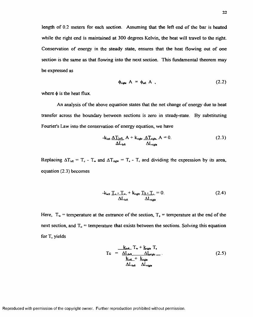
between every section by shifting the temperature references as illustrated in figure 2-1.
Reproduced with permission of the copyright owner. Further reproduction prohibited without permission.
24
Tw Tc— ■ ‘ 1 1
!
0.0 0.2
Tw
Ts
“ o r
Tc
4Ts
0.8 1.0 length (m)
1.2 1.4 1.6 1.8 20
!) .
1i
a d 0.2 0.4 06 0.0 1.0 1.2 1.4 1.6 1.8 2
Tw Tc Ts
2.00.0 0.2 0.4 06 08
Tw Tc
1.0 length (m)
Ts
1.2 1.4 1.6
00 02 04 06 08 10“ 1.2length (m)
1.4 1.6 1.8 20
Figure 2-1: Shifting temperature references to calculate junction temperatures.
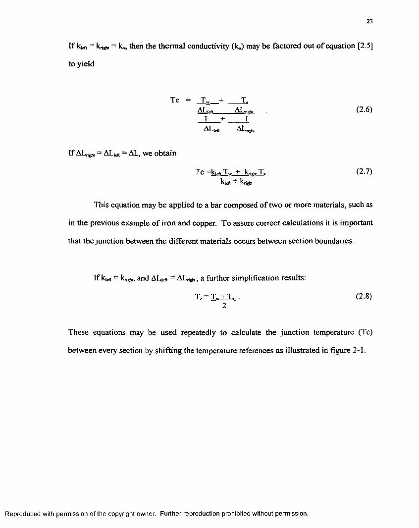
The electrical model represents each section of the bar as an electrical resistance
and the temperatures as voltage sources. This model is presented schematically as figure
2 - 2 .
1 R1 2 R2 3 R3 ( R4 5 R5 5 R8 7 R7 3 no o ra io mu iir-WWVu— W /W v— Wfb— W W t t r - W M — — WWVv— W M — W f o — WW U,1
yltai Vaniiert j
Figure 2-2: Electrical model for conduction heat transfer.
Reproduced with permission of the copyright owner. Further reproduction prohibited without permission.
25
Resistance values are computed according to the length and material properties of
the corresponding section. The magnitudes o f these resistance values assure the proper
distribution of the potential difference between Vheat and Valient at the voltage nodes
(representing the section junctions). Details on this electrical analogue will be presented
and discussed in the next chapter.
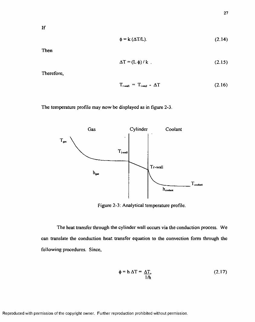
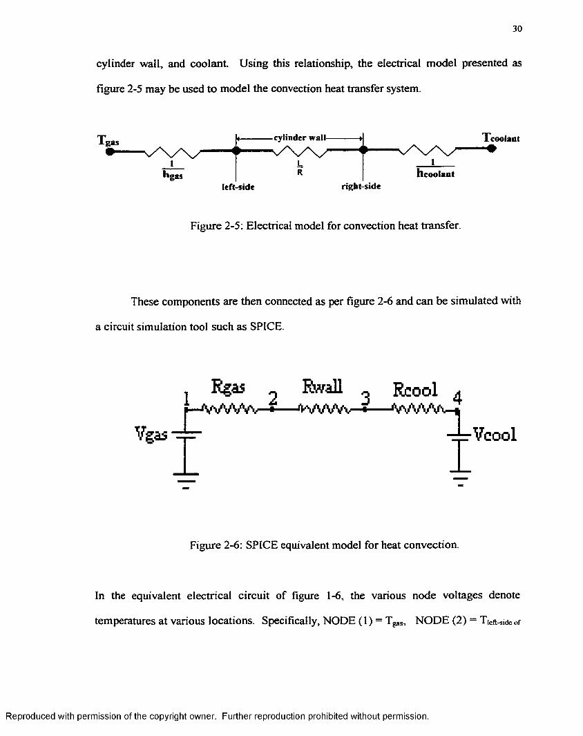
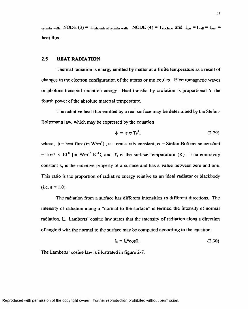
2.4 HEAT CONVECTION
Convection heat transfer through gases and liquids from a solid boundary results
from the fluid motion along the surface. Newton's Equation may quantify the rate of
energy transfer from the system to the fluid as
<|> = h (T .-T r), (2.9)
where, Tf = fluid temperature, Ts = surface temperature, and h = the convection
coefficient.
In order to elaborate on this mechanism, an analysis is presented that examines heat
transfer between a gas and a coolant through a cylinder wall. This problem consists of
three heat transfer functions, a conduction transfer through the cylinder wall, and two
convection heat transfers between the wall surface and the moving mediums. In order to
derive the total heat flux, one needs to calculate the total convection heat transfer
coefficient and temperature change across all three mediums. The total heat flux (<j>) may
be calculated as
^ = Qtoul (Tg*. - T oUm) = (Tp,. - TcqqLmm)__ , (2.10)1 + 1 + 1
hga hw.il hcoolant
Reproduced with permission of the copyright owner. Further reproduction prohibited without permission.
26
with = k/L being the conduction heat transfer through the cylinder wall, h ^ =
convection heat transfer coefficient for the gas, = gas temperature, =
convection heat transfer coefficient for the coolant, = coolant temperature, and
= the total heat transfer occurring through all three mediums.
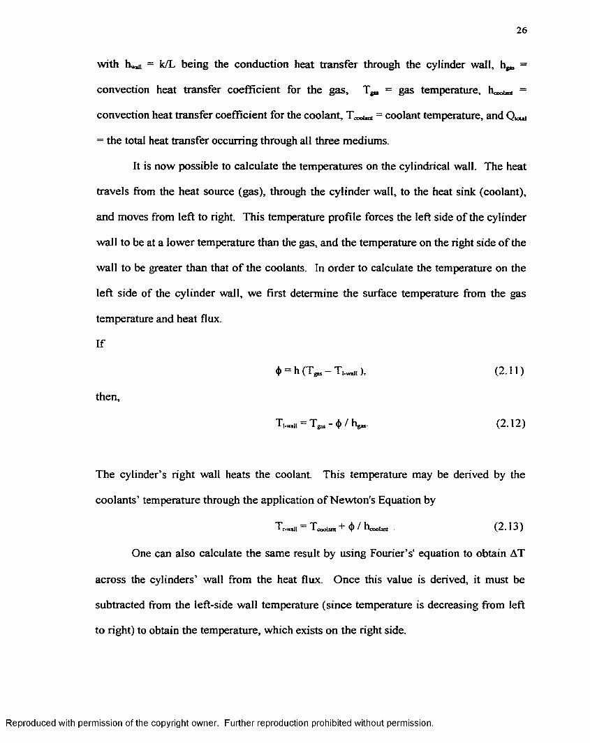
It is now possible to calculate the temperatures on the cylindrical wall. The heat
travels from the heat source (gas), through the cylinder wall, to the heat sink (coolant),
and moves from left to right. This temperature profile forces the left side of the cylinder
wall to be at a lower temperature than the gas, and the temperature on the right side o f the
wall to be greater than that o f the coolants. In order to calculate the temperature on the
left side of the cylinder wall, we first determine the surface temperature from the gas
temperature and heat flux.
If
(|) = h (T gK- T l.wl,), (2.11)
then,
T,.w,„ = T ^ - <{> / hg*,. ( 2 . 1 2 )
The cylinder’s right wall heats the coolant. This temperature may be derived by the
coolants’ temperature through the application of Newton's Equation by
T[--wall Tcoo(am + <|> / hcooian, (2.13)
One can also calculate the same result by using Fourier’s' equation to obtain AT
across the cylinders’ wall from the heat flux. Once this value is derived, it must be
subtracted from the left-side wall temperature (since temperature is decreasing from left
to right) to obtain the temperature, which exists on the right side.
Reproduced with permission of the copyright owner. Further reproduction prohibited without permission.
If
Then
<J) = k (AT/L).
27
(2.14)
Therefore,
AT = (L <|>) / k
Tp-wall ~ T uwuj - AT
(2.15)
(2.16)
The temperature profile may now be displayed as in figure 2-3.
Gas Cylinder Coolant
T1 gas
T r-w all
Figure 2-3: Analytical temperature profile.
- coolant
The heat transfer through the cylinder wall occurs via the conduction process. We
can translate the conduction heat transfer equation to the convection form through the
following procedures. Since,
<t> = h AT = AT.1/h
(2.17)
Reproduced with permission of the copyright owner. Further reproduction prohibited without permission.
28
and
I = <J> A = AV G. (2 .1 8 )
The thermal expression for convection heat transfer can be transformed into the electrical
equivalent expression
<j) A = AV G, (2.19)
where, G = h = G nd - By replacing G ^ with its' equivalent derivation equation, one
obtains
<j> A = AV ([A k] / L). (2 .2 0 )
Upon dividing both sides o f the equation by its area, the heat flux of the thermal model is
obtained, which represents the current for the electrical model. This flux is given by
(j) = AV Gcond = A V ( k / L). (2 .2 1 )
Since,
G , ^ = 1 /R c o n d , (2 .22)
the resistance may now be computed as
R w a ll = 1 /G conduction = L / k . ( 2 . 2 j )
The second type o f heat transfer action occurs through the gas layer, which lies
between the surface of the wall and the moving medium. This heat transfer process is
illustrated as figure 2-4.
Reproduced with permission of the copyright owner. Further reproduction prohibited without permission.
Figure 2-4: Convection heat transfer.
The heat transfer coefficient (h) depends on the type of fluid and the fluid
velocity. If we relate Fourier’s Law o f heat conduction to Newton's equation, we obtain
kAT = hAT. (2.24)L
The value of h may now be derived by dividing both sides of the equation by AT, to
obtain
h = k/L . (2.25)
Comparing this function to the previously derived equation for conduction resistance
(equation [2.23]), leads to
R = 1/h. (2.26)
Consequently, resistances on both sides o f the cylinder wall can now be computed as
Rg«=l/hgM , and (2.27)
Rcoolam = 1/hxwiju,, . (2.28)
In order to model the heat transfer through the cylinder wall electrically, a series
resistance circuit is created. The temperatures of the gas and coolant are modeled by DC
voltage sources. Series connected resistors model the thermal resistance o f the gas layer,
Reproduced with permission of the copyright owner. Further reproduction prohibited without permission.
30
cylinder wall, and coolant Using this relationship, the electrical model presented as
figure 2-5 may be used to model the convection heat transfer system.
Tcoolantcylinder wallgas
hcoolant'gasright-sideleft-side
Figure 2-5: Electrical model for convection heat transfer.
These components are then connected as per figure 2-6 and can be simulated with
a circuit simulation tool such as SPICE.
Rgas „ Ewall „ Rcool 4i—A M / W v —■------ W W W - * W W V w
- -JV cool
Figure 2-6: SPICE equivalent model for heat convection.
In the equivalent electrical circuit of figure 1-6, the various node voltages denote
temperatures at various locations. Specifically, NODE (1) = TgaS, NODE (2) = Tieft-a.de of
Vgas
Reproduced with permission of the copyright owner. Further reproduction prohibited without permission.
31
cylinder wall, NODE (3) Tnght-side o f cylinder wall, NODE (4) TcoolanU <Uld Igas I wail Icool
heat flux.
2.5 HEAT RADIATION
Thermal radiation is energy emitted by matter at a finite temperature as a result o f
changes in the electron configuration of the atoms or molecules. Electromagnetic waves
or photons transport radiation energy. Heat transfer by radiation is proportional to the
fourth power of the absolute material temperature.
The radiative heat flux emitted by a real surface may be determined by the Stefan-
Boltzmann law, which may be expressed by the equation
<j> = e ct Ts4, (2.29)
where, <j) = heat flux (in W/m2) , e = emissivity constant, a = Stefan-Boltzmann constant
= 5.67 x 10'8 [in Wm'2 fC4], and Ts is the surface temperature (K). The emissivity
constant e, is the radiative property of a surface and has a value between zero and one.
This ratio is the proportion o f radiative energy relative to an ideal radiator or blackbody
(i.e. e = 1.0).
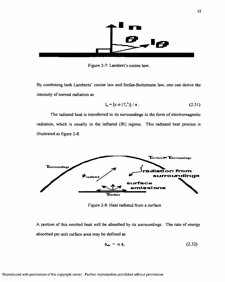
The radiation from a surface has different intensities in different directions. The
intensity of radiation along a “normal to the surface” is termed the intensity of normal
radiation, In. Lamberts’ cosine law states that the intensity o f radiation along a direction
o f angle 0 with the normal to the surface may be computed according to the equation:
Ie = In*cos0. (2.30)
The Lamberts’ cosine law is illustrated in figure 2-7.
Reproduced with permission of the copyright owner. Further reproduction prohibited without permission.
32
Figure 2-7: Lambert’s cosine law.
By combining both Lamberts’ cosine law and Stefan-Boltzmann law, one can derive the
intensity of normal radiation as
I„ = [ e a ( T s4)]/7 t. (2.31)
The radiated heat is transferred to its surroundings in the form o f electromagnetic
radiation, which is usually in the infrared (IR) regime. This radiated heat process is
illustrated as figure 2-8.
■surroundings
0radiated
■surfaced* ^surroundings
■ radiation fromsurroundings
surfaceamissions
■surface
Figure 2-8: Heat radiated from a surface.
A portion of this emitted heat will be absorbed by its surroundings. The rate of energy
absorbed per unit surface area may be defined as
<t>» = oo<|>, (2.32)
Reproduced with permission of the copyright owner. Further reproduction prohibited without permission.
33
where a is the absorptivity constant. This proportionality constant is a dimensionless
value representing the fraction of incident radiation that is absorbed by its surroundings.
As the object’s surface temperature rises, it emits greater radiation and warms its
surroundings. As the emitted radiation increases, so does the absorbed radiation.
Therefore, the net radiated heat is a function of both its surface and surrounding
temperatures. The radiation equations are now presented as
Remitted = 8 cr (Tobj,*,4), (2 .33)
Rabaorbed = 6 O’ (Tnitroundings X (2-34)
Rnet Remitted Rabaorbed > and (2.35)
R** = 8 cr (Tobj«4 - T*,,™^4). (2.36)
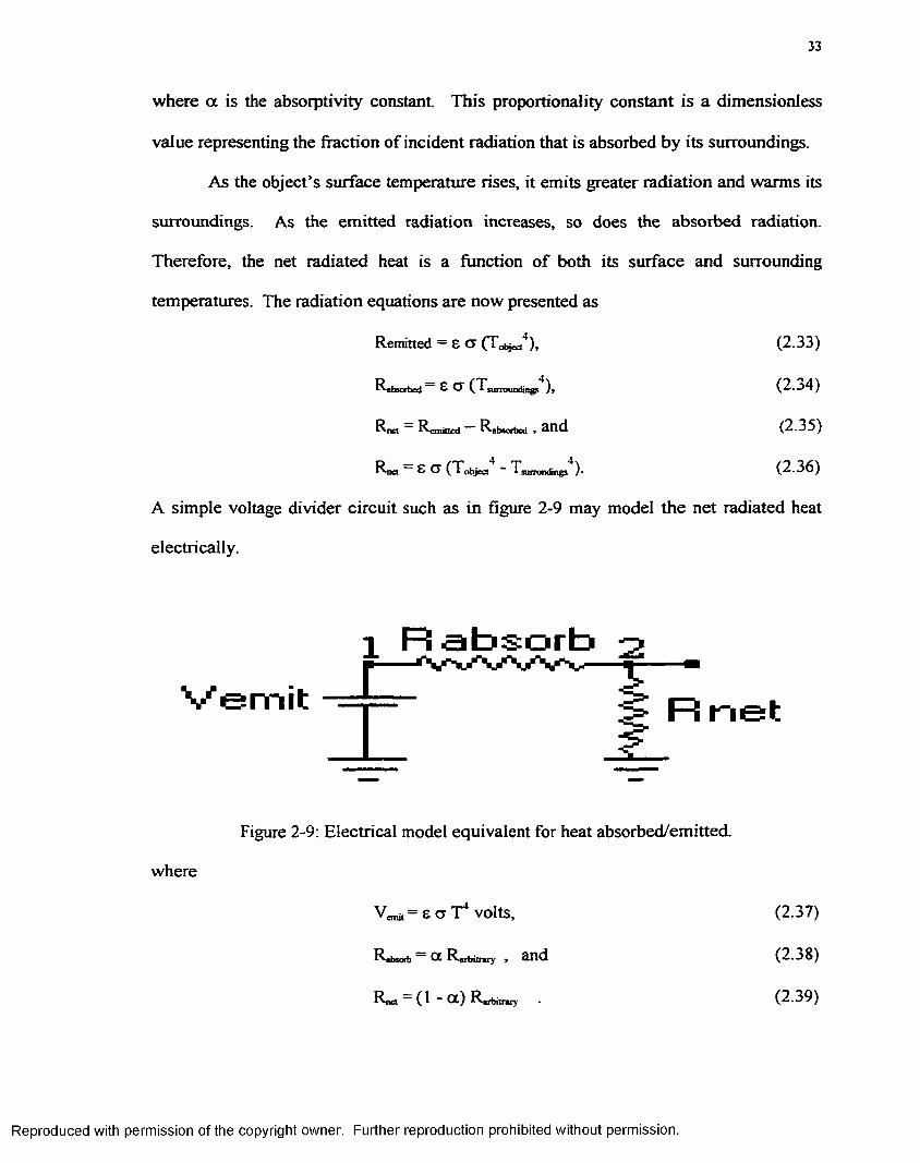
A simple voltage divider circuit such as in figure 2-9 may model the net radiated heat
electrically.
1 R absorb o— ^ w v v w
V emit R net
where
Figure 2-9: Electrical model equivalent for heat absorbed/emitted.
V.™, = e ct T4 volts,
Rabsorb Ct Rartritrary , and
Rnet ( 1 ” Cl) Rubitrary
(2.37)
(2.38)
(2.39)
Reproduced with permission of the copyright owner. Further reproduction prohibited without permission.
34
The value of the arbitrary resistance is o f little significance, since it just ensures
the proper voltage to heat flux ratio. Maximum emitted heat occurs when the surrounding
temperature is zero degrees Kelvin (a = 0). Calculating the voltage at Rnet using the
voltage divider rule may derive the heat emitted to the surroundings as
When thermal radiation strikes a body, it is either absorbed (a), reflected (p), or
transmitted (x) through the body. Therefore,
Reflectivity and transmissivity are properties o f the body’s surface and are dependent on
the temperature o f the body and the wavelength of the incident radiation. Reflectivity is a
fractional value, which represents the portion of incident radiation, which is reflected
from the body. Rough surfaces are better absorbers and emitters than smooth surfaces.
Transmissivity is that portion o f incident radiation, which is transmitted through the
body. We can now expand our circuit to model the reflected and transmitted thermal
radiation. A portion (p) o f the emitted radiation is reflected from the body and the
remaining is transmitted through the body. Therefore, the equivalent electrical circuit o f
figure 2-10 may be used to accurately represent the thermal radiated heat.
V = V D" n e t v e m i t------ (2.40)
a + p + x = 1 (2.41)
Reproduced with permission of the copyright owner. Further reproduction prohibited without permission.
35
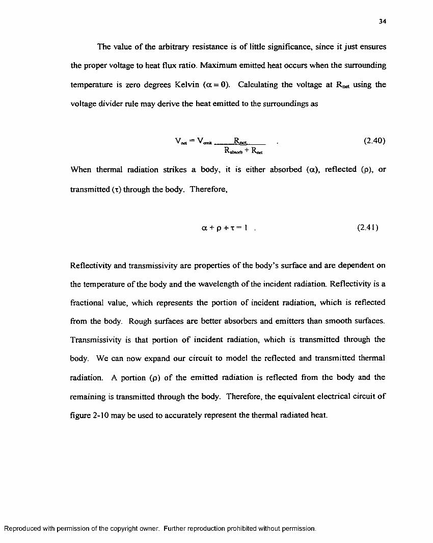
1 R absorb o R reflect 3I— < W W W - M W v w
VemitRnet R transmit
Figure 2-10: Electrical model equivalent for radiated heat.
This circuit forms a series-parallel network, with Rabsorb in series with R«, in
parallel, with the series combination o f R«ncct and R^ w . The reflected and transmitted
radiations are products o f the emitted radiation, and therefore, should not affect the
quantity o f radiation to be absorbed or emitted. In order to effectively isolate and
R<rznsmit from the emission circuit, one must choose a value o f R.~i .. which is much, much
greater than the value o f Rotary.
The maximum resistance of a parallel network cannot exceed that o f the smallest
resistance o f the network. By using a very large value of R;„..,~. with respect to Rotary, the
series combination of Rrcnecl and Ru™,* places a large resistance in parallel with R**, so
that the parallel resistor combination is approximately equal to R^. Since R^, resistance
remains approximately the same, the emitted voltage does not vary. The heat transmitted
through the body may be derived similarly as the emitted heat by another application of
the voltage divider rule. This yields:
r e tr a n s m it •
^ tra n sm it R rcflect
(2.42)
Reproduced with permission of the copyright owner. Further reproduction prohibited without permission.
36
CHAPTER III
METHODOLOGY AND IMPLEMENTATION
3.1 INTRODUCTION
The equivalence between the thermal system o f equations and the variables o f circuit
theory, immediately suggests the use o f circuit simulators for the solution o f the thermal
problem. Based on a finite difference discretization o f the heat flow equation, an
equivalence between the electrical and thermal systems can be shown.
As a result, a differential element o f volume within the semiconductor material
denoting a unit cell for the thermal problem can be presented in terms o f an equivalent
electrical building block. This repetitive block would consist of two serial resistors with
a parallel combination o f a current source and a capacitor connected between them.
Obviously, for 2D or 3D analysis, one would have four- or six- resistors, respectively.
These building blocks would be interconnected to yield the volume of the entire structure.
This equivalent electrical network could be solved for a given set of current excitations,
using the commercially available SPICE simulator yielding all nodal voltages as a
function of time. Since SPICE programs are available, and are capable of handling a
large number of nodes, the thermal problem could be solved exactly.
Such equivalent electrical circuit simulations have been used for thermal analysis
[23, 24]. This approach can easily be generalized to include the temperature dependence
o f the thermal conductivity and specific heat by employing voltage controlled resistor and
capacitor elements. Since voltage controlled elements are available within the SPICE
simulator, this extension should be trivial. The added advantage is that in addition to
time-domain analysis, the technique would easily furnish the frequency response
Reproduced with permission of the copyright owner. Further reproduction prohibited without permission.
37
characteristics based on the built-in capability of the SPICE simulation tool. Details o f
this technique and the mathematics leading to the SPICE based analysis are presented and
discussed next in this chapter.
3.2 ELECTRICAL ANALOG OF THE THERMAL SYSTEM
The heat flow equation for a one-dimensional sample with uniform thermal
conductivity may be expressed by the equation
k (dT2/dx2) + g = pCp (dT/dt). (3.1)
Assigning a new variable AT = T — T0, the equation becomes:
k (d2AT/dx2) + g = pCp (AT/dt). (3.2)
Equivalence between the variables o f the thermal system and an electrical circuit can be
invoked through the following transformations:
V(x) = T(x), (3.3)Is (x) = A Ax g(x), (3.4)C(x) = A Ax p Cp, (3.5)AV(x) = AT(x) = T(x) - To, (3.6)G(x) = A (k/Ax), and (3.7)R(x) = 1/G(x) = Ax/{A k} . (3.8)
In the above equations (3.3)-(3.8), A is the cross-sectional area, Ax the length of each
discretized segment, Is(x) a position-dependent equivalent current source, C a
capacitance, AV(x) a potential difference between segments of the equivalent circuit,
G(x) a conductance element, and R(x) the electrical resistance of each segment. Using
this equivalent transformation, the governing equation for thermal transport (3.2) can be
expressed in terms o f current flow within an electrical circuit. The resulting equation is:
Reproduced with permission of the copyright owner. Further reproduction prohibited without permission.
38
G A2 (d2 V/dx2)+ Is (x) = C (dV(x)/dt) (3.9)
3.2.1 THERMAL RESISTANCE
Thermal resistance is the reciprocal o f its conductance and can be used as a
measure of the insulation quality. The thermal (Rt) and electrical resistance (R«)
equations are given as
The units for equation (3.10) are expressed in degrees Kelvin per Watt. In the
electrical model, 1 Watt of energy relates to 1 Ampere o f electrical current and one
degree Kelvin corresponds to one Volt o f electrical potential. So by replacing Watts with
Amperes and degrees Kelvin with volts, the correct expression for electrical resistance
(the Ohm) is obtained as Volts per Ampere.
Since the heat flow equation is a second-order differential equation, one needs to
impose two boundary conditions for a solution. A Dirichlet boundary condition for a
constant temperature translates into a fixed node voltage at the appropriate boundary.
This can easily be implemented by assigning a very small electrical resistance value
between the boundary node and its neighbors). Here, for instance, in a one-dimensional
(ID) analysis with the Dirichlet boundary taken to be at the x = 0 endpoint, a resistance
Ri o f 10'5 Ohms was assigned for a numerical implementation. This low resistance
would ensure (as shown later through actual simulation results), that nodes 1 and 2 were
sustained at approximately the same voltage. Boundary conditions o f the Neumann type,
dT/dx |(o, o = 0 correspond to adiabatic conditions, and essentially require zero heat flux.
Rt = Ax/{A k}, and (3.10)
Rc = (p Ax)/A. (3.11)
Reproduced with permission of the copyright owner. Further reproduction prohibited without permission.
39
In the electrical equivalent, this corresponds to an adequate representation o f zero current.
For these purposes, the electrical resistance between such a boundary node and its
neighbors was taken to have a very large value. Here, a resistance termed Ropen o f 1011
Ohms magnitude was assumed to adequately represent this desired condition. The large
value o f Ropen would cause very little current flow, essentially leading to an electrically
open circuit at the boundary.
3.2.2 CAPACITANCE
The specific heat o f the bar needs to be modeled electrically as a capacitance in
the equivalent electrical analogue. A material’s specific heat defines the number o f
Joules required to raise the temperature of one gram o f the material one degree Kelvin,
and is mathematically defined as
Q = m Cp AT. (3.12)
Dividing both sides o f the equation by AT and replacing the temperature with its
electrical equivalent of a voltage, the new equation becomes
Q/V = m Cp. (3.13)
The mass is the product of the material’s area, subsection length Ax, and density p, i.e. m
= A Ax p. Since the capacitance is defined to be the ratio o f the charge to voltage (i.e. C
= QfV), one gets
C = Q/V = m C p = A A x p C p , (3.14)
in direct verification o f equation (3.5) given previously.
Reproduced with permission of the copyright owner. Further reproduction prohibited without permission.
40
3.2.3 CURRENT SOURCES
The current sources in the electrical model simulate the conduction heat flow.
Heat flows in the direction of high to low temperature. Thus for a simple ID case with
the left end maintained at a higher temperature, heat travels from x = 0 to x = L. The
total heat applied to the bar is the product o f the applied heat per unit volume (g) and the
volume o f the bar. Since the heat is evenly distributed along the length o f the bar, the
amount o f current added per sub-section is such that the total current flowing out o f a
particular node is the summation o f the currents from all previous nodes.
A conversion from heat flux to an electrical current can be applied to validate the
relationship between the models. The amount of heat flux per sub-section may be derived
through Fourier’s Law o f heat conduction by the equation
(j) = -k (AT/AL). (3.15)
Conservation of energy ensures that no heat loss occurs when flowing between sub
sections (between nodes of the electrical circuit). As the heat flow continues down the
length of the bar, each sub-section contributes its own amount of heat flow (represented
electrically as the current sources) which is cumulative between sub-sections. Therefore,
the heat flux and electrical current are at their maximum at the final sub-section. The
electrical current is given by Ohm’s Law as
I = AV G. (3.16)
Replacing G with its’ thermal equivalent expression (equation 3.7), one obtains
I = AV {A (k/Ax)}. (3.17)
By converting Fourier’s Law into its electrical equivalent components, equation (3.17)
may be expressed in terms o f the flux, <j>, as
Reproduced with permission of the copyright owner. Further reproduction prohibited without permission.
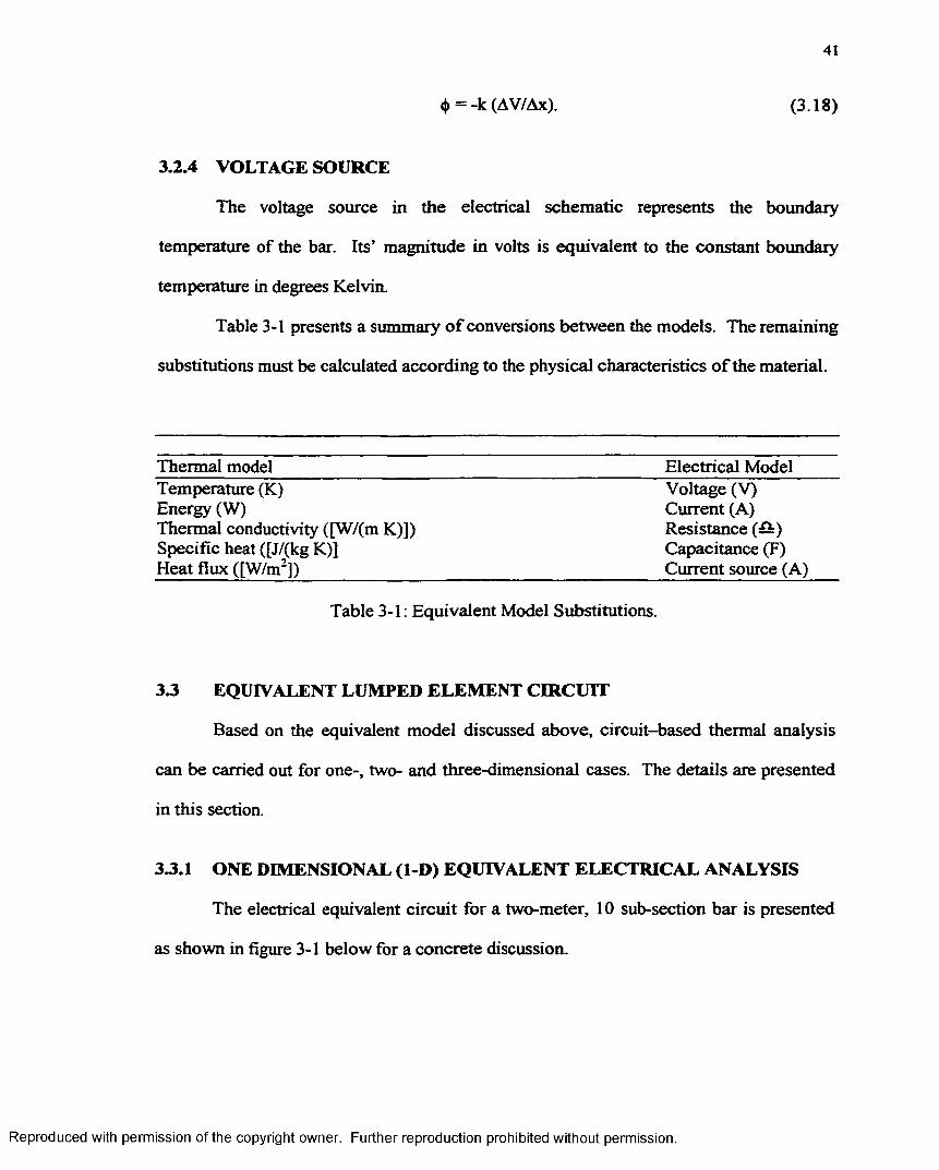
41
<J) = -k (AV/Ax). (3.18)
3.2.4 VOLTAGE SOURCE
The voltage source in the electrical schematic represents the boundary
temperature of the bar. Its’ magnitude in volts is equivalent to the constant boundary
temperature in degrees Kelvin.
Table 3-1 presents a summary o f conversions between the models. The remaining
substitutions must be calculated according to the physical characteristics o f the material.
Thermal model Electrical ModelTemperature (K) Voltage (V)Energy (W) Current (A)Thermal conductivity ([W/(m K)]) Resistance (S )Specific heat ([J/(kg K)] Capacitance (F)Heat flux ([W/m2]) Current source (A)
Table 3-1: Equivalent Model Substitutions.
3.3 EQUIVALENT LUMPED ELEMENT CIRCUIT
Based on the equivalent model discussed above, circuit-based thermal analysis
can be carried out for one-, two- and three-dimensional cases. The details are presented
in this section.
33.1 ONE DIMENSIONAL (1-D) EQUIVALENT ELECTRICAL ANALYSIS
The electrical equivalent circuit for a two-meter, 10 sub-section bar is presented
as shown in figure 3-1 below for a concrete discussion.
Reproduced with permission of the copyright owner. Further reproduction prohibited without permission.
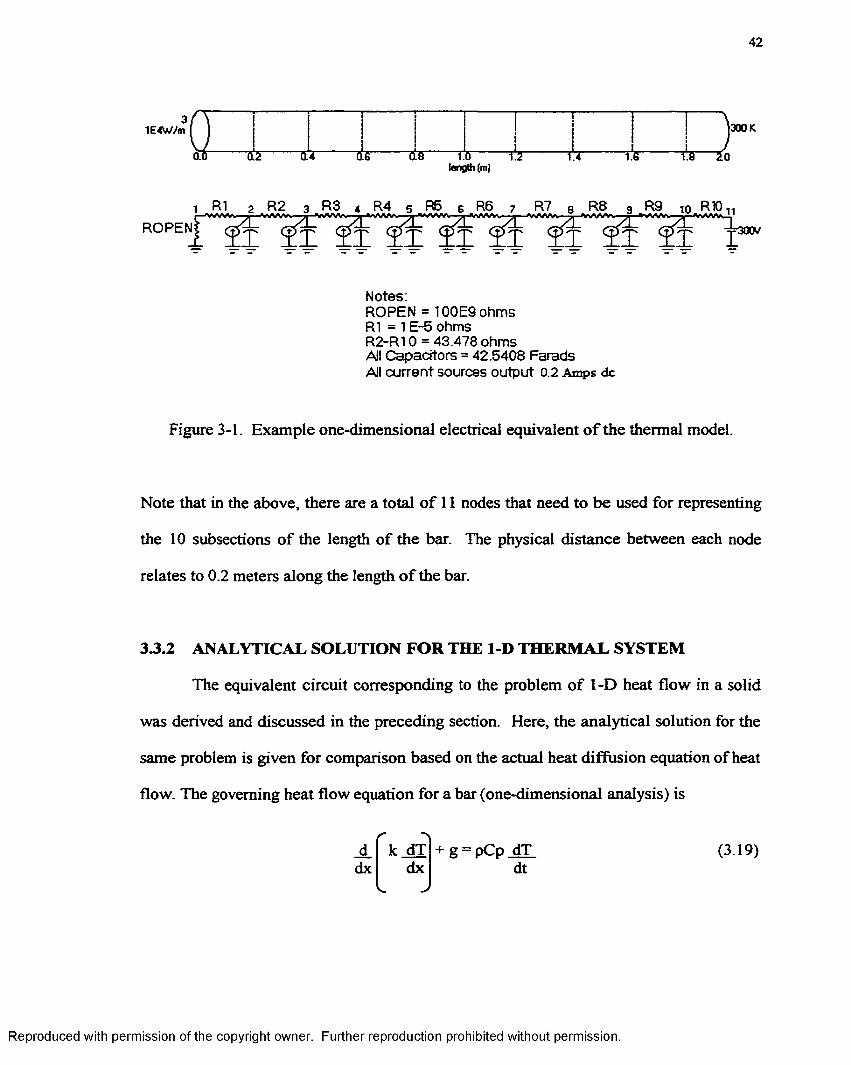
42
31E4Wma |300 K
112 T 5T TtT ~05~ ” T 5 ------length (mj
T F I T 176 t a 2o
i R1 2 R2 3 R3 4 R4 5 R5 6 R6 7 R7 8 R8 9 R9 1 0 RIO,,. VWVWw ». ■■■■-Vs/WW ■ -»- VAWv WAM .w »VWV» . ' 'ROPEN£ (7j?p <?^k t T f t p 300
Notes:ROPEN = 100E9 ohmsR1 = 1E-5 ohmsR2-R10 = 43.478 ohmsAll Capacitors = 42.5408 FaradsAll current sources output 0.2 Amps dc
Figure 3-1. Example one-dimensional electrical equivalent o f the thermal model.
Note that in the above, there are a total o f 11 nodes that need to be used for representing
the 10 subsections o f the length o f the bar. The physical distance between each node
relates to 0.2 meters along the length o f the bar.
3.3.2 ANALYTICAL SOLUTION FOR THE 1-D THERMAL SYSTEM
The equivalent circuit corresponding to the problem o f 1-D heat flow in a solid
was derived and discussed in the preceding section. Here, the analytical solution for the
same problem is given for comparison based on the actual heat diffusion equation of heat
flow. The governing heat flow equation for a bar (one-dimensional analysis) is
_d_dx
k dT dx
+ g = pCp dT dt
(3.19)
Reproduced with permission of the copyright owner. Further reproduction prohibited without permission.
43
where,
g = heat generation per unit volume, p = density of material,Cp = specific heat, and k = thermal conductivity.
For a constant/uniform “k,” the above equation becomes
Assigning: u(x, t) = X(x) * T(t), the following differential equation results:
Solving this equation by separation of variables under the boundary conditions of
Since u(x, t) = X(x) * T(t), multiplying these two functions together yields the
transient solution:
The initial steady-state condition has a uniform temperature, Ta throughout the
bar, therefore
Reproduced with permission of the copyright owner. Further reproduction prohibited without permission.
k_d2T + g = pCpdT (3.20)dt
k X” T + g = p Cp X T \ (3.21)
dT/dx (0, t) = 0, and T(L, t) = To, (3.22)
yields
X(x) = cos 2m+l)7t (3.23)
and
T(t) = exp Fa(2m +n27rt (3.24)
^-af2m+l )2tt2tJcos ^2m+1 hexJ (3.25)
T(x, 0) = Ttt (3.26)
44
Since the partial differential equation and boundary conditions are linear and
homogeneous, the function
u(x,0) = Bn cos pm -H htx^ , (3.27)[ 2 L J
satisfies the solution for arbitrary constants B„ at t = 0.
Solving for the Fourier Coefficients yields
m = ao
B„ = -16gL2 2 ( - n m . (3.28)ki t3 m = 0 (2m+l)
If we now insert this coefficient into our equation, the resulting transient
expression becomes
m = co 2 v* / 1 \mu(x,t) = -16eL 2 f - i r exp
k 7t3 m = 0 (2m + l)-a(2m+H2 tc2 t COS (2m+l):cx4L2 J L 2L J . (3.29)
We can now solve for the steady state function. At steady state the rate o f change
o f time is zero, thereby reducing equation (3.20) to
k d^L + g = 0 . (3.30)dx2
Solving this differential equation under the boundary conditions o f equation (3.22) yields
the steady state bar temperatures o f
T (x) = _g_ (L2 - X2) + T0 . (3.31)2k
The complete heat expression is the summation of the transient and steady state
equations. Adding these two equations together, yields the final equation for temperature
as a function of x and t as
m = a o
T(x, t) = g_ (L2 - X V Tn-16L2g 2 f-lV" exp ta t2m + n2 7t2 t 1 cos [2m±I)7txl(3.32) 2k k7t3 m = 0(2m +l)3 C 41? J C 2L J
Reproduced with permission of the copyright owner. Further reproduction prohibited without permission.
45
If the heat source is removed (g = 0) at time t = toff, the bar begins to cool. The
cooling heat flow equation now becomes
m=oofT(x, t) = T0 + E exp -a(2m-H)2 rc2 (t-t g-)
m=0 4L,m cos 2m-H)7tx
2L(3.33)
The magnitude o f Cm is the temperature above ambient at the instant the heat source is
removed (t = toff) and is derived from the equation
(3.34)r
Cra= 2 [ T (x, t) - T0 ] cos '2m+1 )7tx
L (_0 L 2L J
The above equations will be used later in this chapter to obtain analytical
solutions for the temperature distribution across a 1-D bar. These results, which
represent the exact solution for the actual thermal problem, will be compared with the
predictions o f the equivalent electrical model developed here. Through these
comparisons, it will be shown that the electrical analogue yields identical results and
hence, is a valid scheme for numerical calculations for general problems in heat
conduction.
3.3.3 TWO-DIMENSIONAL ANALYSIS
Placing a vast quantity o f parallel lines side-by-side (zero distance between them)
intersecting an equal number o f perpendicular lines o f the same length and spacing, forms
a solid 2-dimensional plane. This methodology is used to model a two-dimensional
sample. Each line represents a one-dimensional sample analyzed previously. The points
at which the lines intersect are where a common node is shared along both axes. This
Reproduced with permission of the copyright owner. Further reproduction prohibited without permission.
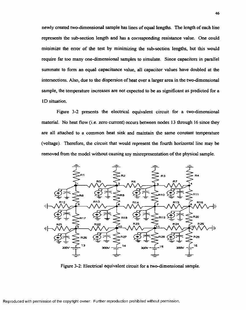
46
newly created two-dimensional sample has lines of equal lengths. The length of each line
represents the sub-section length and has a corresponding resistance value. One could
minimize the error o f the test by minimizing the sub-section lengths, but this would
require far too many one-dimensional samples to simulate. Since capacitors in parallel
summate to form an equal capacitance value, all capacitor values have doubled at the
intersections. Also, due to the dispersion of heat over a larger area in the two-dimensional
sample, the temperature increases are not expected to be as significant as predicted for a
ID situation.
Figure 3-2 presents the electrical equivalent circuit for a two-dimensional
material. No heat flow (i.e. zero current) occurs between nodes 13 through 16 since they
are all attached to a common heat sink and maintain the same constant temperature
(voltage). Therefore, the circuit that would represent the fourth horizontal line may be
removed from the model without causing any misrepresentation o f the physical sample.
R12 R135if-VWV
i h V W V
Figure 3-2: Electrical equivalent circuit for a two-dimensional sample.
Reproduced with permission of the copyright owner. Further reproduction prohibited without permission.
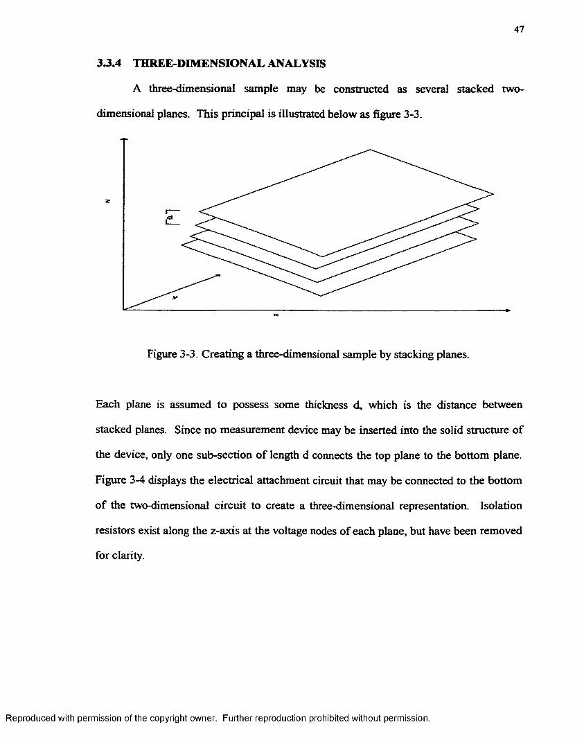
47
3 3 .4 THREE-DIMENSIONAL ANALYSIS
A three-dimensional sample may be constructed as several stacked two-
dimensional planes. This principal is illustrated below as figure 3-3.
x
Figure 3-3. Creating a three-dimensional sample by stacking planes.
Each plane is assumed to possess some thickness d, which is the distance between
stacked planes. Since no measurement device may be inserted into the solid structure o f
the device, only one sub-section o f length d connects the top plane to the bottom plane.
Figure 3-4 displays the electrical attachment circuit that may be connected to the bottom
o f the two-dimensional circuit to create a three-dimensional representation. Isolation
resistors exist along the z-axis at the voltage nodes of each plane, but have been removed
for clarity.
Reproduced with permission of the copyright owner. Further reproduction prohibited without permission.
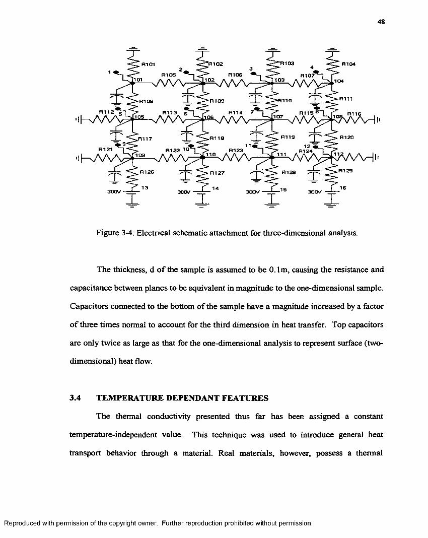
48
R104
0112 5 , r ~,i | - W V V ^ f J!S- v V S A '
RIOT
R107
RillR109
k w v ^ 1' s A A ^ ^ V N A H
R117
R121 I R122 10
' i K / W vR129R126
Figure 3-4: Electrical schematic attachment for three-dimensional analysis.
The thickness, d o f the sample is assumed to be 0.1m, causing the resistance and
capacitance between planes to be equivalent in magnitude to the one-dimensional sample.
Capacitors connected to the bottom o f the sample have a magnitude increased by a factor
o f three times normal to account for the third dimension in heat transfer. Top capacitors
are only twice as large as that for the one-dimensional analysis to represent surface (two-
dimensional) heat flow.
3.4 TEMPERATURE DEPENDANT FEATURES
The thermal conductivity presented thus far has been assigned a constant
temperature-independent value. This technique was used to introduce general heat
transport behavior through a material. Real materials, however, possess a thermal
Reproduced with permission of the copyright owner. Further reproduction prohibited without permission.
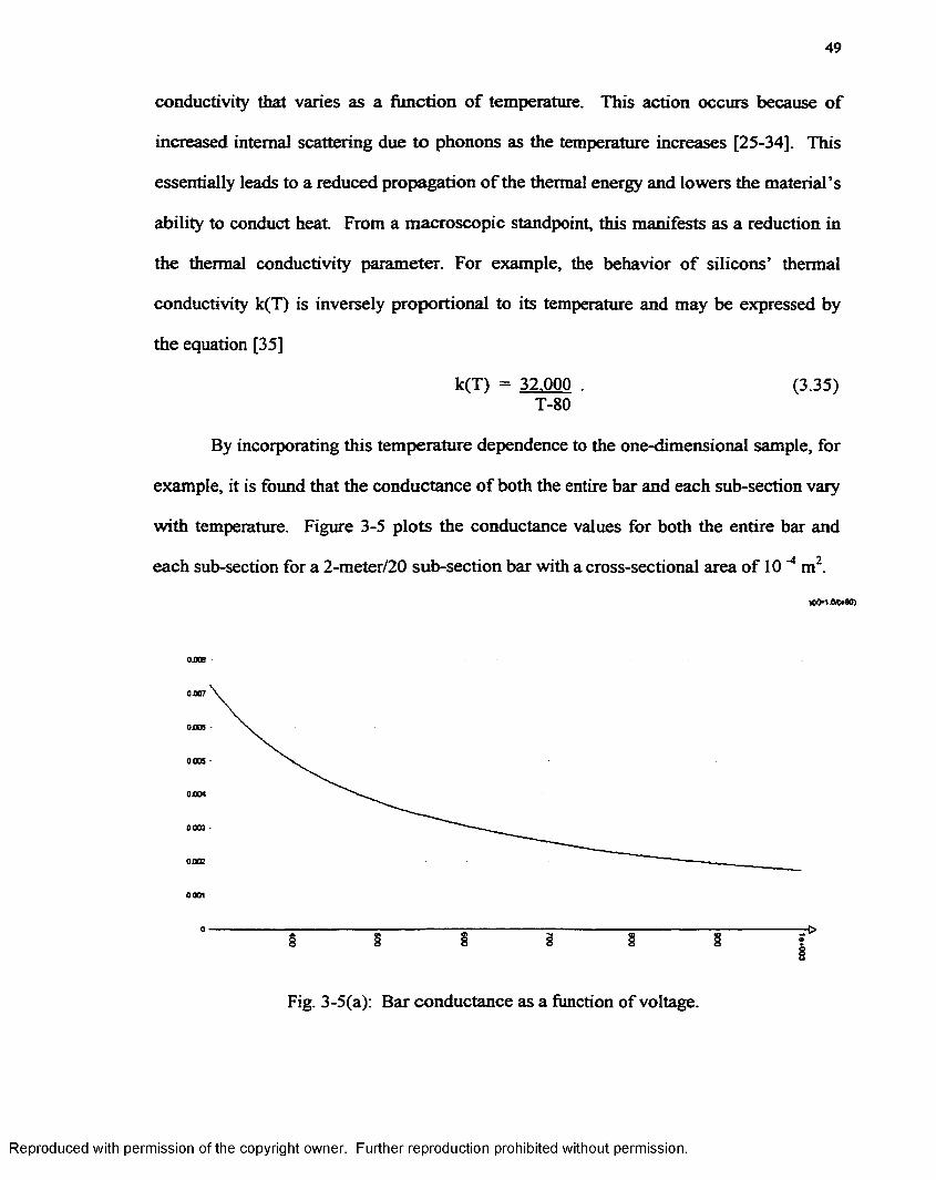
49
conductivity that varies as a function o f temperature. This action occurs because o f
increased internal scattering due to phonons as the temperature increases [25-34], This
essentially leads to a reduced propagation o f the thermal energy and lowers the material’s
ability to conduct heat From a macroscopic standpoint this manifests as a reduction in
the thermal conductivity parameter. For example, the behavior o f silicons’ thermal
conductivity k(T) is inversely proportional to its temperature and may be expressed by
the equation [35]
k(T) = 32.000 . (3.35)T-80
By incorporating this temperature dependence to the one-dimensional sample, for
example, it is found that the conductance o f both the entire bar and each sub-section vary
with temperature. Figure 3-5 plots the conductance values for both the entire bar and
each sub-section for a 2-meter/20 sub-section bar with a cross-sectional area o f 10 ^ m2.
jWi-flfttao)
0003 •
§ § § § § §
Fig. 3-5(a): Bar conductance as a function o f voltage.
Reproduced with permission of the copyright owner. Further reproduction prohibited without permission.
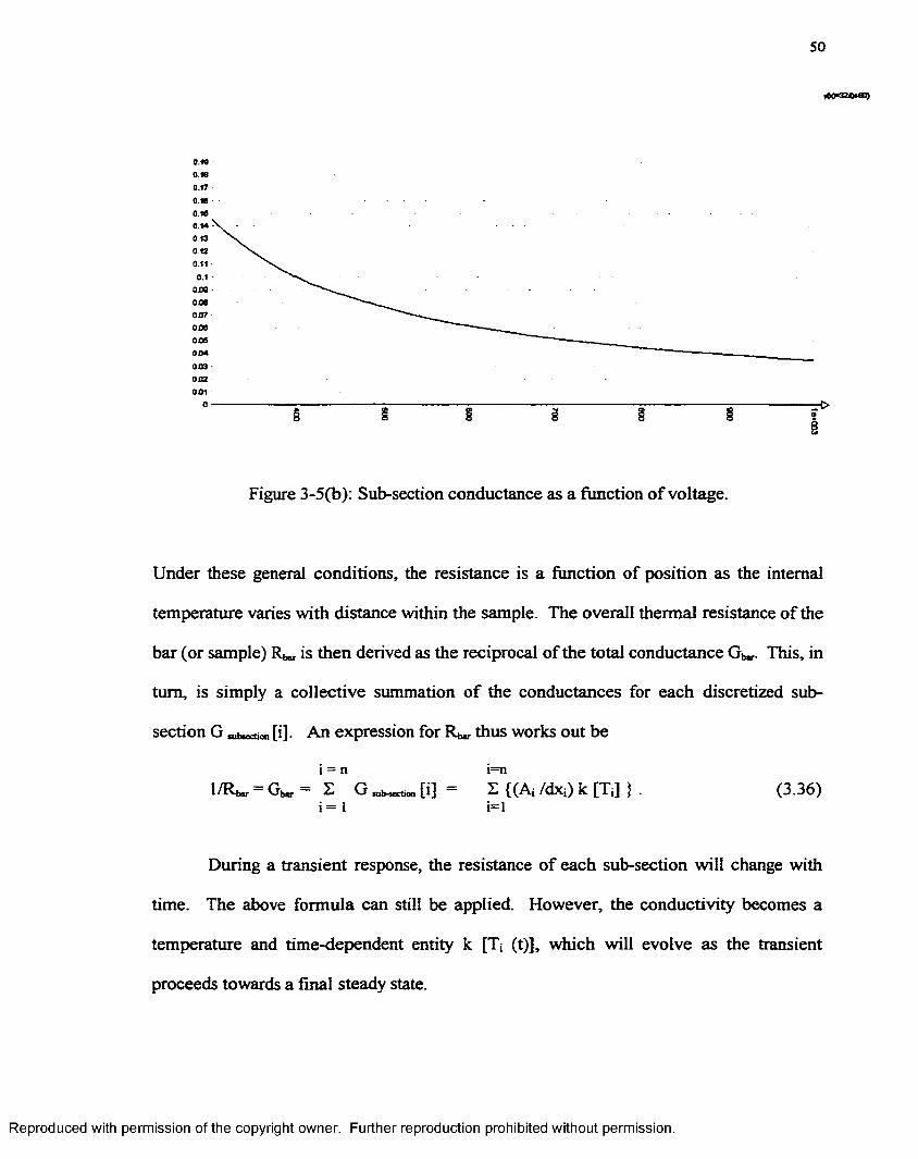
50
Itt"3 2 * 4 0 )
0.10 -
0.18 0.17
0.18 - 0 1 6
003 •
0 jQ2
0 61
0 I § I i i I
Figure 3-5(b): Sub-section conductance as a function o f voltage.
Under these general conditions, the resistance is a function of position as the internal
temperature varies with distance within the sample. The overall thermal resistance o f the
bar (or sample) is then derived as the reciprocal o f the total conductance G ^. This, in
turn, is simply a collective summation o f the conductances for each discretized sub
section G [i]. An expression for thus works out be
i = n i=nl/Rb«r = Gb,r = £ G [i] = £ {(Ai /dxi) k [Ti] } . (3.36)
i = l i=l
During a transient response, the resistance of each sub-section will change with
time. The above formula can still be applied. However, the conductivity becomes a
temperature and time-dependent entity k [Ti (t)], which will evolve as the transient
proceeds towards a final steady state.
Reproduced with permission of the copyright owner. Further reproduction prohibited without permission.
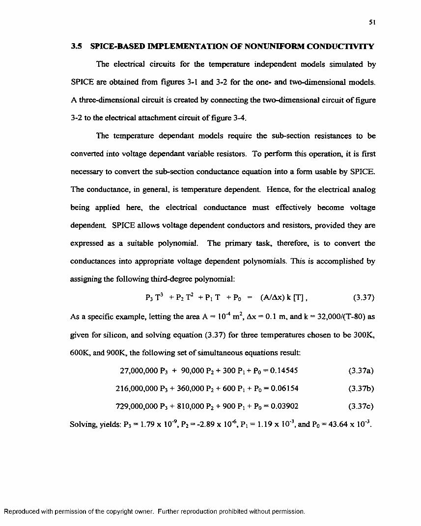
51
3.5 SPICE-BASED IMPLEMENTATION OF NONUNIFORM CONDUCTIVITY
The electrical circuits for the temperature independent models simulated by
SPICE are obtained from figures 3-1 and 3-2 for the one- and two-dimensional models.
A three-dimensional circuit is created by connecting the two-dimensional circuit o f figure
3-2 to the electrical attachment circuit o f figure 3-4.
The temperature dependant models require the sub-section resistances to be
converted into voltage dependant variable resistors. To perform this operation, it is first
necessary to convert the sub-section conductance equation into a form usable by SPICE.
The conductance, in general, is temperature dependent. Hence, for the electrical analog
being applied here, the electrical conductance must effectively become voltage
dependent. SPICE allows voltage dependent conductors and resistors, provided they are
expressed as a suitable polynomial. The primary task, therefore, is to convert the
conductances into appropriate voltage dependent polynomials. This is accomplished by
assigning the following third-degree polynomial:
P3T3 + P 2T2 + P ! T + P 0 = (A/Ax) k [T ], (3.37)
As a specific example, letting the area A = 10"* m2, Ax = 0.1 m, and k = 32,000/(T-80) as
given for silicon, and solving equation (3.37) for three temperatures chosen to be 300K,
600K, and 900K, the following set of simultaneous equations result:
27,000,000 P3 + 90,000 P2 + 300 Pi + P0 = 0.14545 (3.37a)
216.000.000 P3 + 360,000 P2 + 600 P, + P0 = 0.06154 (3.37b)
729.000.000 P3 + 810,000 P2 + 900 Pi + P0 = 0.03902 (3.37c)
Solving, yields: P3 = 1.79 x 10'9, P2 = -2.89 x Iff6, P t = 1.19 x Iff3, and P0 = 43.64 x Iff3.
Reproduced with permission of the copyright owner. Further reproduction prohibited without permission.
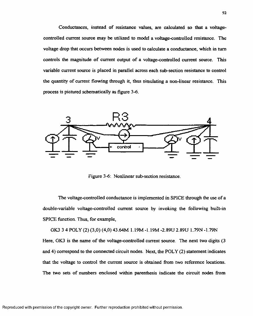
52
Conductances, instead o f resistance values, are calculated so that a voltage-
controlled current source may be utilized to model a voltage-controlled resistance. The
voltage drop that occurs between nodes is used to calculate a conductance, which in turn
controls the magnitude o f current output o f a voltage-controlled current source. This
variable current source is placed in parallel across each sub-section resistance to control
the quantity o f current flowing through it, thus simulating a non-linear resistance. This
process is pictured schematically as figure 3-6.
+ c o n t r o l
Figure 3-6: Nonlinear sub-section resistance.
The voltage-controlled conductance is implemented in SPICE through the use o f a
double-variable voltage-controlled current source by invoking the following built-in
SPICE function. Thus, for example,
GK3 3 4 POLY (2) (3,0) (4,0) 43.64M 1.19M-1.19M-2.89U2.89U 1.79N-1.79N
Here, GK3 is the name o f the voltage-controlled current source. The next two digits (3
and 4) correspond to the connected circuit nodes. Next, the POLY (2) statement indicates
that the voltage to control the current source is obtained from two reference locations.
The two sets of numbers enclosed within parenthesis indicate the circuit nodes from
Reproduced with permission of the copyright owner. Further reproduction prohibited without permission.
53
where the controlling voltages are to be obtained Finally, the string o f numbers that
follow correspond to the magnitude at which to adjust the current source as determined
by the conductance difference between the nodes. This voltage controlled current source
is placed across each sub-section resistance to model a voltage-controlled resistor
(temperature dependant thermal conductivity) along each axis of every model.
3.6 SIMPLE TEST CASE FOR A VALIDITY CHECK
Validation o f the electrical model begins by comparing the results o f a 2-meter,
10-node electrical model presented in figure 3-1 to the equivalent thermal model.
3.6.1 INITIAL CONDITIONS
Initially, the bar is in an environment with a uniform temperature o f 300K. In the
equivalent electrical model, the capacitors are fully charged to that of the voltage source
(i.e. a constant 300V representing the 300 K temperature). When the capacitors are fully
charged, no current flows in the electrical circuit. The initial condition is displayed in the
partial schematic o f figure 3-7 between circuit nodes 9 through 11. Notice that the
current sources are represented as open circuits indicating that they are turned off in the
absence o f any external excitation or thermal input
Applying K irchoffs current law at each loop o f the circuit yields the nodal
voltages at this time. Figures 3-8 and 3-9 verify this steady-state condition with the
SPICE simulator.
Reproduced with permission of the copyright owner. Further reproduction prohibited without permission.
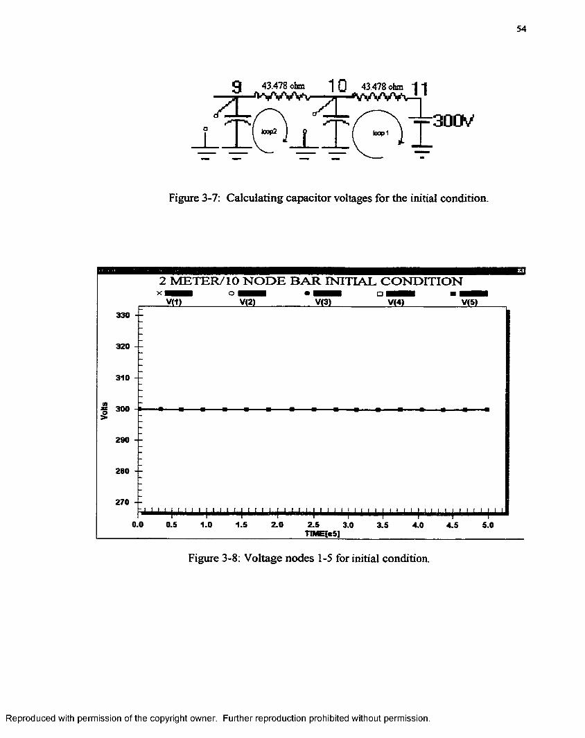
Volts
54
43.478 ohm
ioop2
43.478 ohm 11W W v A 1
= k 3 0 0 V
Figure 3-7: Calculating capacitor voltages for the initial condition.
2 M E T E R / 1 0 N O D E B A R I N I T I A L C O N D I T I O No ■ ■ ■ ■ • H B B
XfiSL330 - -
310 - -
300
290 - -
280 - -
270 - -
0.0 0.5 1.0 1.5 2.0 2.5 3.0 5.03.5 4.0 4.5TtWg[eS]
Figure 3-8: Voltage nodes 1-5 for initial condition.
Reproduced with permission of the copyright owner. Further reproduction prohibited without permission.
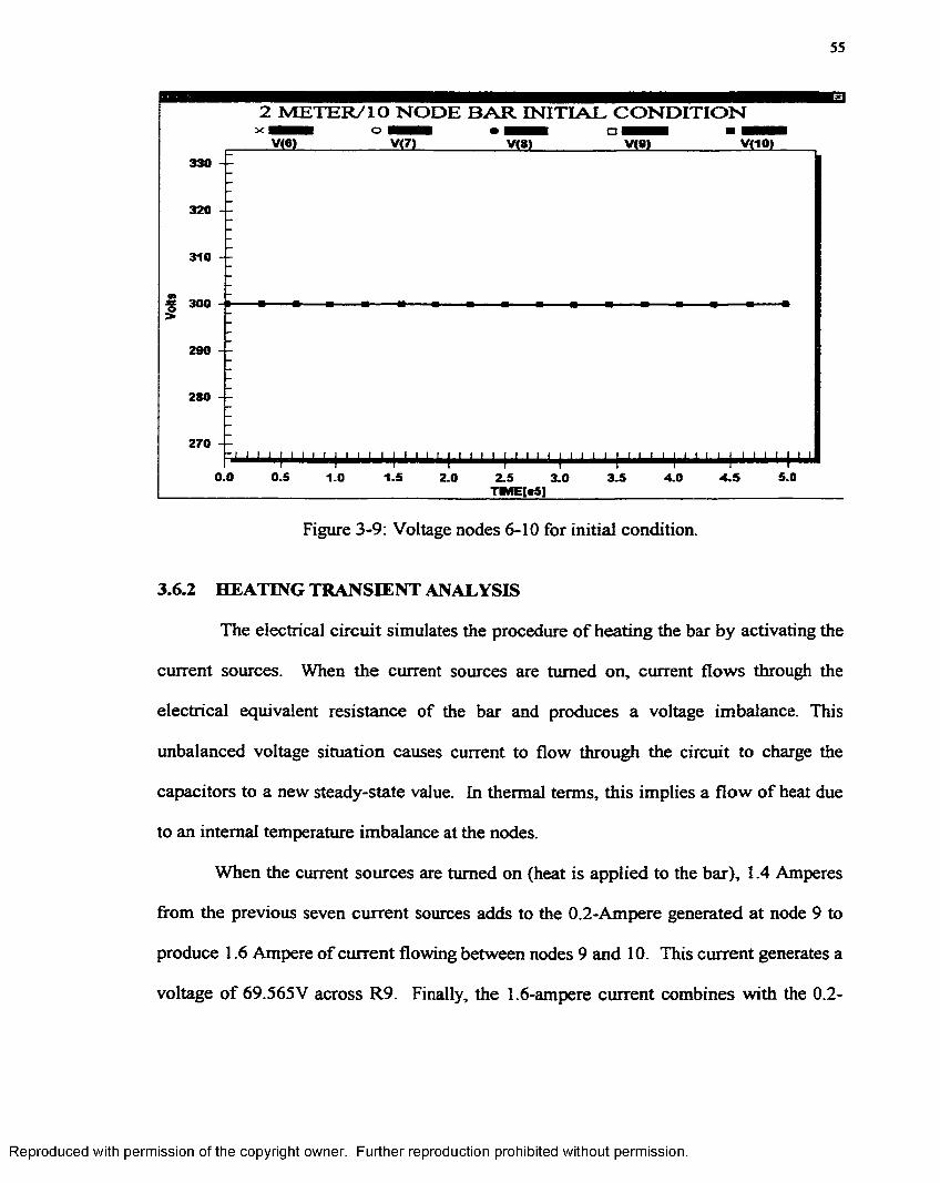
55
2 METER/lO NODE BAR INITIAL CONDITION
320
310
01? 300
290 - -
280 - -
270 - -
0.0 0.5 1.5 5.03.5 4.0 4 .51.0 2.0 3.0
Figure 3-9: Voltage nodes 6-10 for initial condition.
3.6.2 HEATING TRANSIENT ANALYSIS
The electrical circuit simulates the procedure o f heating the bar by activating the
current sources. When the current sources are turned on, current flows through the
electrical equivalent resistance of the bar and produces a voltage imbalance. This
unbalanced voltage situation causes current to flow through the circuit to charge the
capacitors to a new steady-state value. In thermal terms, this implies a flow o f heat due
to an internal temperature imbalance at the nodes.
When the current sources are turned on (heat is applied to the bar), 1.4 Amperes
from the previous seven current sources adds to the 0.2-Ampere generated at node 9 to
produce 1.6 Ampere of current flowing between nodes 9 and 10. This current generates a
voltage o f 69.565V across R9. Finally, the 1.6-ampere current combines with the 0.2-
Reproduced with permission of the copyright owner. Further reproduction prohibited without permission.
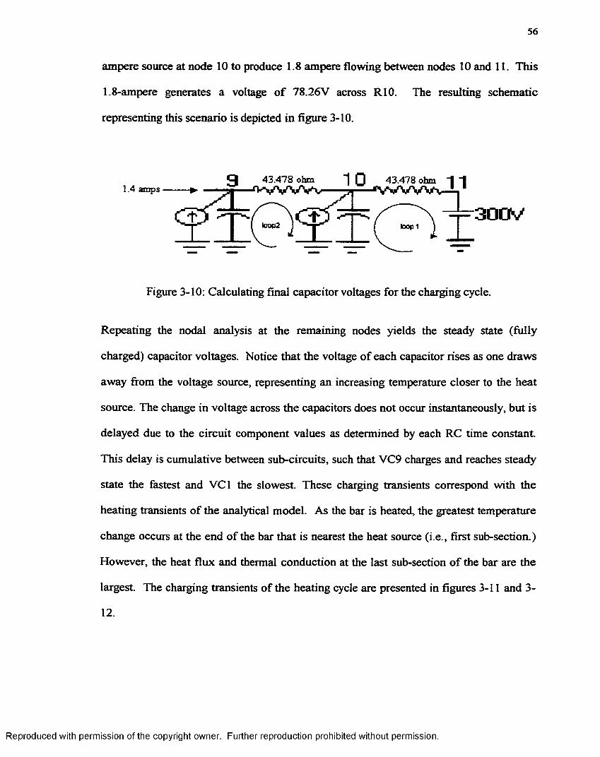
56
ampere source at node 10 to produce 1.8 ampere flowing between nodes 10 and 11. This
1.8-ampere generates a voltage o f 78.26V across RIO. The resulting schematic
representing this scenario is depicted in figure 3-10.
Q 43.478 ohm 71— f V V W W1.4 amps
loop 1
Figure 3-10: Calculating final capacitor voltages for the charging cycle.
Repeating the nodal analysis at the remaining nodes yields the steady state (fully
charged) capacitor voltages. Notice that the voltage o f each capacitor rises as one draws
away from the voltage source, representing an increasing temperature closer to the heat
source. The change in voltage across the capacitors does not occur instantaneously, but is
delayed due to the circuit component values as determined by each RC time constant.
This delay is cumulative between sub-circuits, such that VC9 charges and reaches steady
state the fastest and VC1 the slowest. These charging transients correspond with the
heating transients o f the analytical model. As the bar is heated, the greatest temperature
change occurs at the end o f the bar that is nearest the heat source (i.e., first sub-section.)
However, the heat flux and thermal conduction at the last sub-section o f the bar are the
largest. The charging transients of the heating cycle are presented in figures 3-11 and 3-
12.
Reproduced with permission of the copyright owner. Further reproduction prohibited without permission.
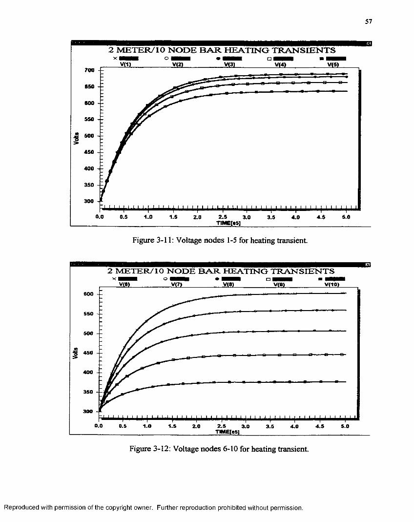
57
2 M E T E R /1 0 N O D E B A R H E A T IN G T R A N S IE N T Sx ■■■■ o ■■■§ • ■■■■ Q H H ■ ■ ■
m
vm.700
850
800
550
m■g3*
500
450
400
350
300
0.0 0.5 1.0 2.51.5 4.5 5.02.0 3.0 3.5 4.0TIMEfcS]
Figure 3-11: Voltage nodes 1-5 for heating transient.
2 M E T E R /10 N O D E B A R H E A T IN G T R A N S IE N T Sx o • ■■■■ a h MHH ■ ■■■
VW______________ V(7)______________ VJ8J______________V(fl)______________V(10)
600
550
500
•t% 450
400
350
300
0.0 0.5 1.0 1.5 2.5TIME[c5]
5.02.0 3.0 4.53.5 4.0
Figure 3-12: Voltage nodes 6-10 for heating transient.
Reproduced with permission of the copyright owner. Further reproduction prohibited without permission.
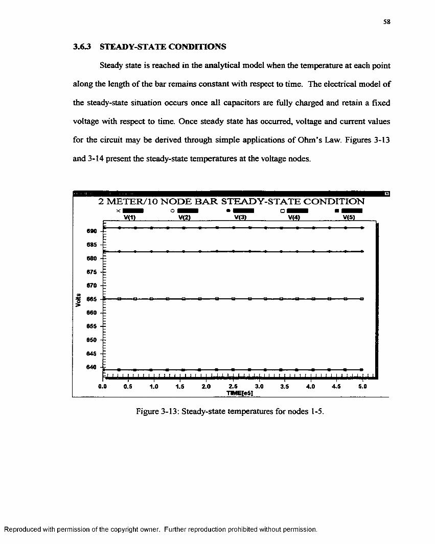
58
3.6.3 STEADY-STATE CONDITIONS
Steady state is reached in the analytical model when the temperature at each point
along the length of the bar remains constant with respect to time. The electrical model o f
the steady-state situation occurs once all capacitors are fully charged and retain a fixed
voltage with respect to time. Once steady state has occurred, voltage and current values
for the circuit may be derived through simple applications o f Ohm’s Law. Figures 3-13
and 3-14 present the steady-state temperatures at the voltage nodes.
■ E
2 M E T E R / 1 0 N O D E B A R S T E A D Y - S T A T E C O N D I T I O N
v e ivf?l690
685
680
675
670
665
660
655
650
645
640
0.0 3.0 4.5 5.00.5 1.0 1.5 2.0 3.5 4.0
Figure 3-13: Steady-state temperatures for nodes 1-5.
Reproduced with permission of the copyright owner. Further reproduction prohibited without permission.
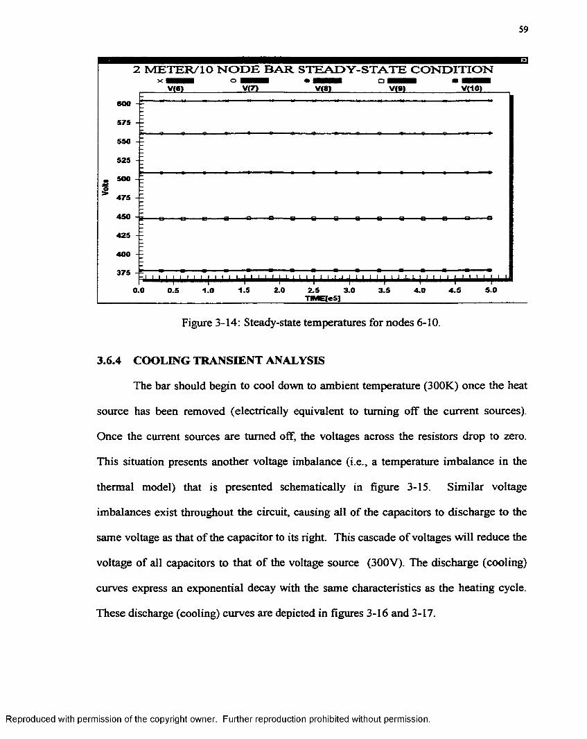
59
2 METER/lO NODE BAR STEADY-STATE CONDITIONx o BBHB • BBBM q B^HB ■ BH^^BV(g)__________VJZ)______________VJ81______________ Vi?)______________v<io)
575
550
525
• 500
475
450 -j.
425
400
375 - -
5.01.5 2.0 4.50.0 2.5T1MEI«S]
3.0 3.51.0 4.00.5
Figure 3-14: Steady-state temperatures for nodes 6-10.
3.6.4 COOLING TRANSIENT ANALYSIS
The bar should begin to cool down to ambient temperature (300K) once the heat
source has been removed (electrically equivalent to turning off the current sources).
Once the current sources are turned off, the voltages across the resistors drop to zero.
This situation presents another voltage imbalance (i.e., a temperature imbalance in the
thermal model) that is presented schematically in figure 3-15. Similar voltage
imbalances exist throughout the circuit, causing all o f the capacitors to discharge to the
same voltage as that o f the capacitor to its right. This cascade o f voltages will reduce the
voltage of all capacitors to that o f the voltage source (300V). The discharge (cooling)
curves express an exponential decay with the same characteristics as the heating cycle.
These discharge (cooling) curves are depicted in figures 3-16 and 3-17.
Reproduced with permission of the copyright owner. Further reproduction prohibited without permission.
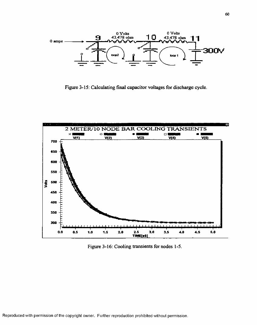
Volts
60
0 am p s
0 Volts 9 43.478 ohm
A V W V v
0 Volts 43.478 ohm “J “|
loop 1= ^ 3 G O V
Figure 3-15: Calculating final capacitor voltages for discharge cycle.
2 METER/10 NODE BAR COOLING TRANSIENTSX O ■ ■ ■ ■ • ■ ■ ■ ■ □ ■ ■ ■ ■ ■ ■ ■
VJ11700
650
BOO
550
500
450
400
350
300
0.0 2.5 3.0 4.5 5.00.5 1.5 2.0 3.5 4.01.0TIMERS]
Figure 3-16: Cooling transients for nodes 1-5.
Reproduced with permission of the copyright owner. Further reproduction prohibited without permission.
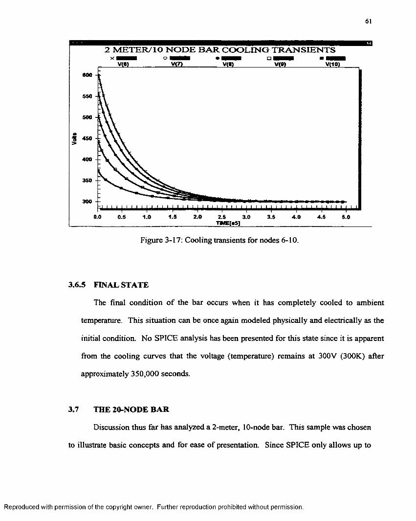
61
2 METER/lO NODE BAR COOLING TRANSIENTS
V<9)
600
550
500
g 450
400
350
300
1.5 2.00.0 1.0 3.5 4.5 5.00.5 3.0 4.0
Figure 3-17: Cooling transients for nodes 6-10.
3.6.5 FINAL STATE
The final condition o f the bar occurs when it has completely cooled to ambient
temperature. This situation can be once again modeled physically and electrically as the
initial condition. No SPICE analysis has been presented for this state since it is apparent
from the cooling curves that the voltage (temperature) remains at 300V (300K) after
approximately 350,000 seconds.
3.7 THE 20-NODE BAR
Discussion thus far has analyzed a 2-meter, 10-node bar. This sample was chosen
to illustrate basic concepts and for ease of presentation. Since SPICE only allows up to
Reproduced with permission of the copyright owner. Further reproduction prohibited without permission.
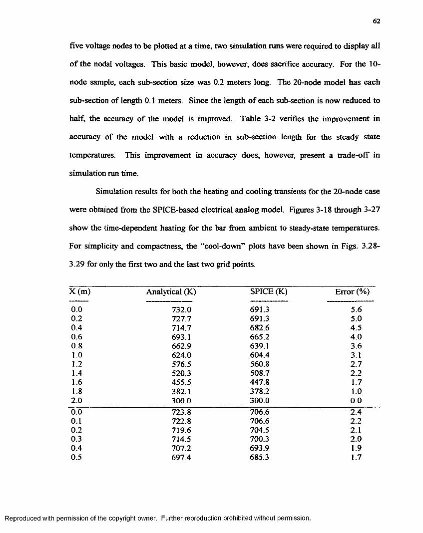
62
five voltage nodes to be plotted at a time, two simulation runs were required to display all
o f the nodal voltages. This basic model, however, does sacrifice accuracy. For the 10-
node sample, each sub-section size was 0.2 meters long. The 20-node model has each
sub-section of length 0.1 meters. Since the length o f each sub-section is now reduced to
half, the accuracy o f the model is improved. Table 3-2 verifies the improvement in
accuracy of the model with a reduction in sub-section length for the steady state
temperatures. This improvement in accuracy does, however, present a trade-off in
simulation run time.
Simulation results for both the heating and cooling transients for the 20-node case
were obtained from the SPICE-based electrical analog model. Figures 3-18 through 3-27
show the time-dependent heating for the bar from ambient to steady-state temperatures.
For simplicity and compactness, the “cool-down” plots have been shown in Figs. 3.28-
3.29 for only the first two and the last two grid points.
X (m) Analytical (K) SPICE (K) Error (%)
0.0 732.0 691.3 5.60.2 727.7 691.3 5.00.4 714.7 682.6 4.50.6 693.1 665.2 4.00.8 662.9 639.1 3.61.0 624.0 604.4 3.11.2 576.5 560.8 2.71.4 520.3 508.7 2.21.6 455.5 447.8 1.71.8 382.1 378.2 1.02.0 300.0 300.0 0.00.0 723.8 706.6 2.40.1 722.8 706.6 2.20.2 719.6 704.5 2.10.3 714.5 700.3 2.00.4 707.2 693.9 1.90.5 697.4 685.3 1.7
Reproduced with permission of the copyright owner. Further reproduction prohibited without permission.
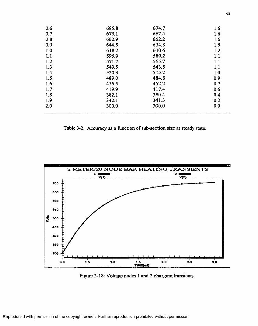
0.6 685.8 674.7 1.60.7 679.1 667.4 1.60.8 662.9 652.2 1.60.9 644.5 634.8 1.5l.O 618.2 610.6 1.21.1 595.9 589.2 1.1l.2 571.7 565.7 1.1l .3 549.5 543.5 1.1l.4 520.3 515.2 1.0l .5 489.0 484.8 0.9l.6 455.5 452.2 0.7l .7 419.9 417.4 0.6l .8 382.1 380.4 0.4l.9 342.1 341.3 0.22.0 300.0 300.0 0.0
Table 3-2: Accuracy as a function of sub-section size at steady state.
2 METER/20 NODE BAR HEATING TRANSIENTSx ■■■■■ o
____________ V£U______________________________ V(21_________700
650
600
550
^ 500
450
400
350
300
0.0 2.01.0 2.50.5 3.0
Figure 3-18: Voltage nodes l and 2 charging transients.
Reproduced with permission of the copyright owner. Further reproduction prohibited without permission.

64
2 METER/2O NODE BAR HEATING TRANSIENTSX ■■■■■ o ■■■■■
_____________Vi?)______________________________Vil)_________700
850
800
550
^ 500
450
400
350
300
2.5 3.00.0 1.0 2.00.5
Figure 3-19: Voltage nodes 3 and 4 charging transients.
2 METER/20 NODE BAR HEATING TRANSIENTS
V(8)700
650
800
550
MI 500
450
400
350
300
3.00.0 1.0 1.5 2.50.5 2.0T1ME|«51
Figure 3-20: Voltage nodes 5 and 6 charging transients.
Reproduced with permission of the copyright owner. Further reproduction prohibited without permission.
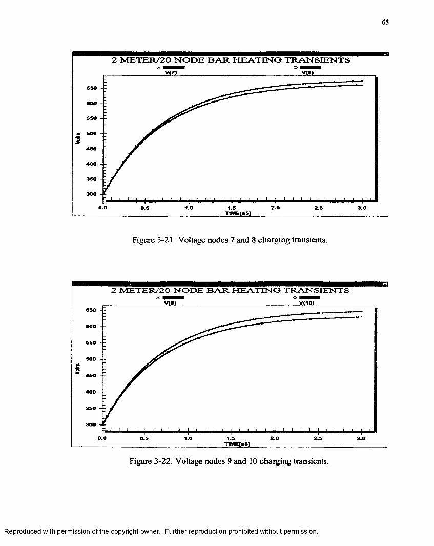
65
2 METER/20 NODE BAR H E A T IN G TRANSIENTSx o
IS
v ia
650
600
550
500
450
400
350
300
0.0 2.01.0 1.6 2.50.5 3.0TBWECeSl
Figure 3-21: Voltage nodes 7 and 8 charging transients.
2 METER/2O NODE BAR HEATING TRANSIENTSxr o
650
600
550
500
t 450
400
350
300
0.0 2.0 2.50.5 1.0 1.5 3.0TIMEIeSl
Figure 3-22: Voltage nodes 9 and 10 charging transients.
Reproduced with permission of the copyright owner. Further reproduction prohibited without permission.
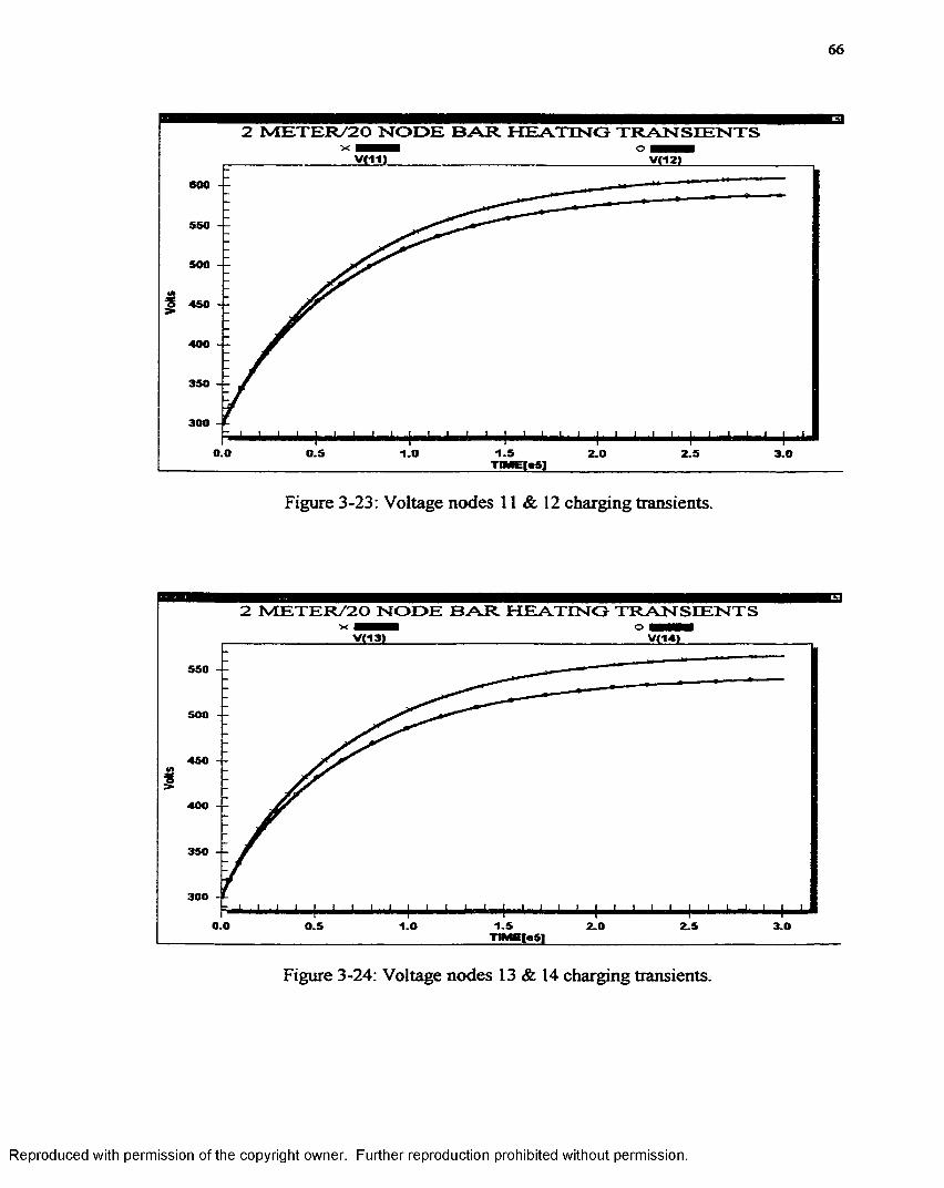
66
2 METER/2O NODE BAR HEATING TRANSIENTSX o ■■■■
__________________V(11)_________________________________________ V(12)____________
600
550
500
■? 450
400
350
300
0.0 0.5 1.0 2.0 2.5 3.0
Figure 3-23: Voltage nodes 11 & 12 charging transients.
2 METER/2O NODE BAR HEATING TRANSIENTSx o ■■■■
550
500
450
*400
350
300
0.0 0.5 1.5 2.51.0 2.0 3.0nWE[«6|
Figure 3-24: Voltage nodes 13 & 14 charging transients.
Reproduced with permission of the copyright owner. Further reproduction prohibited without permission.
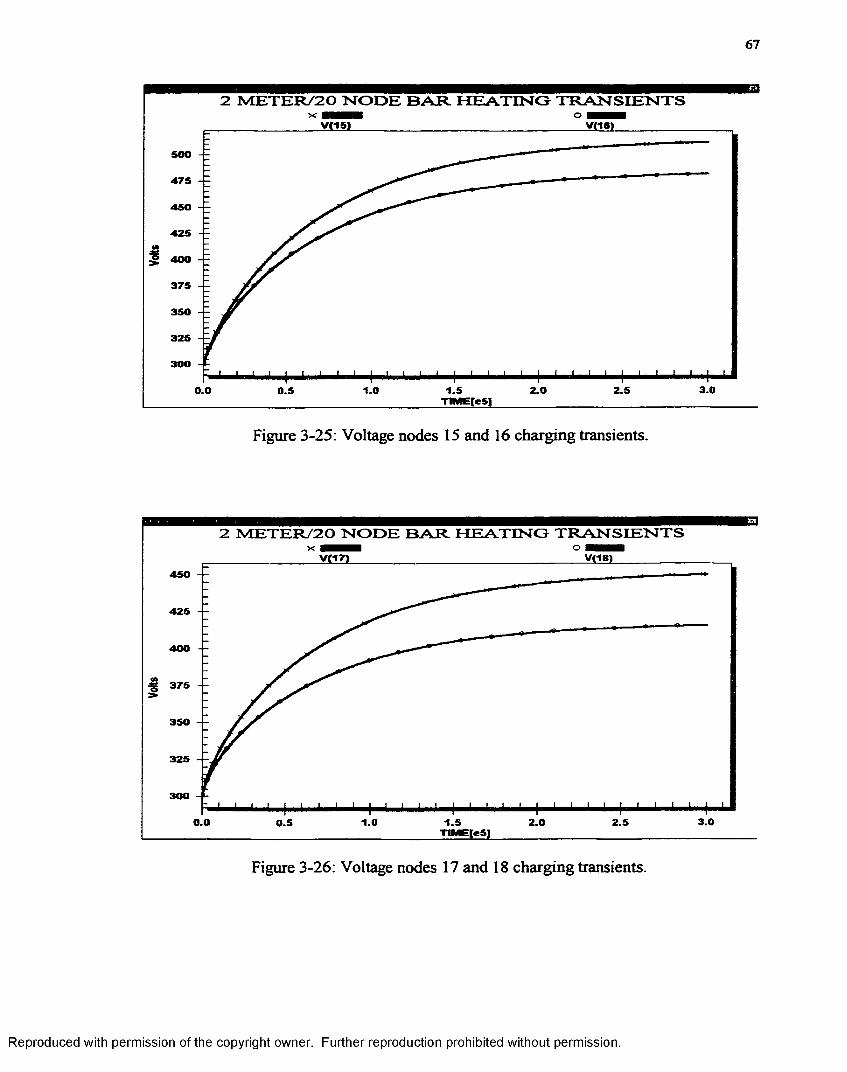
67
2 METER/2O NODE BAR. HEATING TRANSIENTS
500
475
450
425(•* 400
375
350
325
300
3.02.0 2.50.0 1.0 1.50.5TtME[cSl
Figure 3-25: Voltage nodes 15 and 16 charging transients.
2 METER/2O NODE BAR HEATING TRANSIENTS>r O ■■■■
_____________________VC171__________________________________________________V(18)_______________
450
425
400
375
350
325
300
3.02.50.0 1.0 2.00.5
Figure 3-26: Voltage nodes 17 and 18 charging transients.
Reproduced with permission of the copyright owner. Further reproduction prohibited without permission.
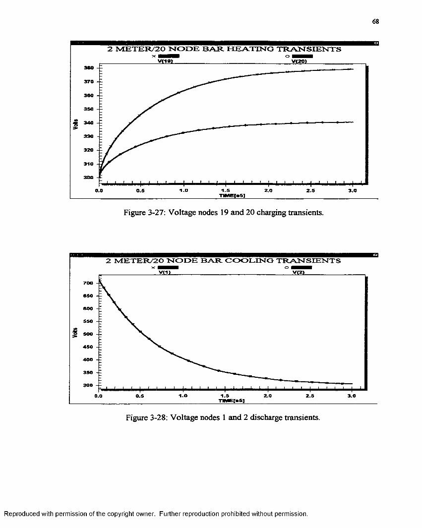
68
2 METER/2O NODE BAR HEATING TRANSIENTS
380
370
360
350
340
330
320
310
300
0.0 1.0 1.5 2.00.5 2.5 3.0TWMg|»Sl
Figure 3-27: Voltage nodes 19 and 20 charging transients.
2 METER/20 NODE BAR COOLING TRANSIENTS
700
650
600
550
3 500
450
350
300
1.0 2.0 2.5 3.00.0 0.5
Figure 3-28: Voltage nodes l and 2 discharge transients.
Reproduced with permission of the copyright owner. Further reproduction prohibited without permission.
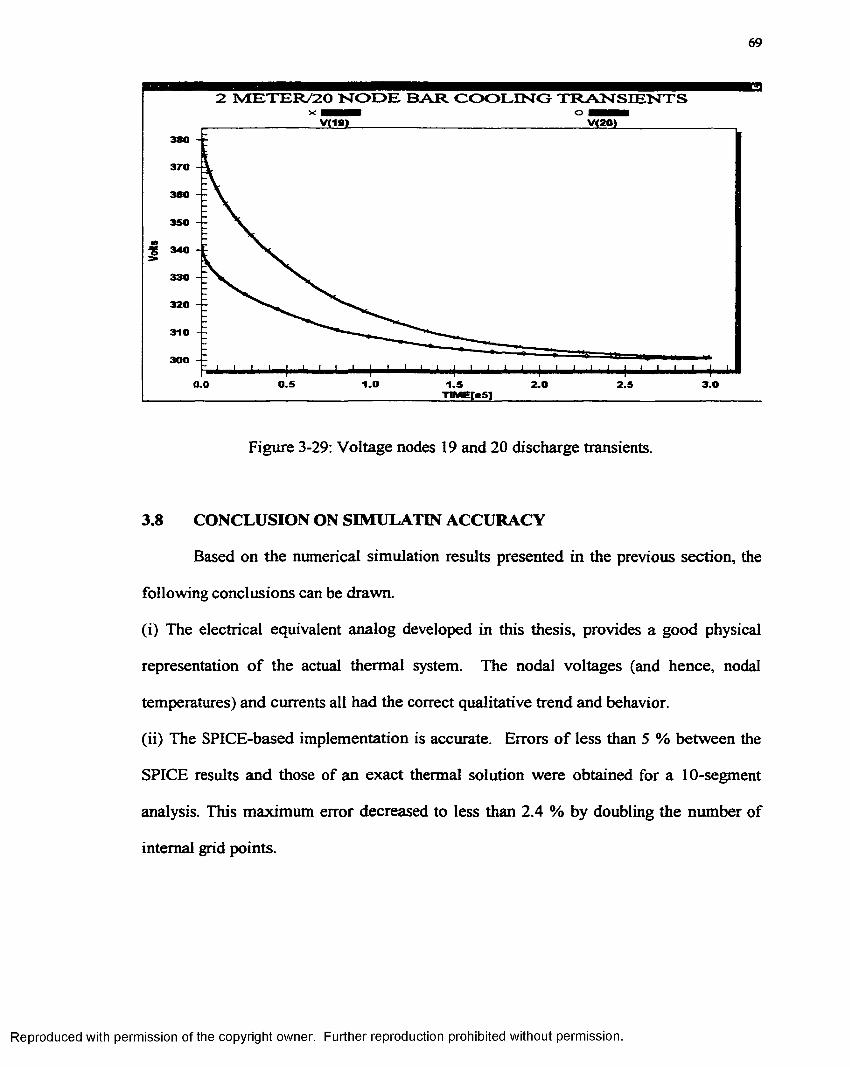
69
2 METER/2O NODE BAR COOLING TRANSIENTSx ■■■■ o
__________________ V(1»1L380
370
300
350
330
320
310
300
0.5 1.00.0 2.0 2.5 3.0
Figure 3-29: Voltage nodes 19 and 20 discharge transients.
3.8 CONCLUSION ON SIMULATES ACCURACY
Based on the numerical simulation results presented in the previous section, the
following conclusions can be drawn.
(i) The electrical equivalent analog developed in this thesis, provides a good physical
representation o f the actual thermal system. The nodal voltages (and hence, nodal
temperatures) and currents all had the correct qualitative trend and behavior.
(ii) The SPICE-based implementation is accurate. Errors o f less than 5 % between the
SPICE results and those of an exact thermal solution were obtained for a 10-segment
analysis. This maximum error decreased to less than 2.4 % by doubling the number of
internal grid points.
Reproduced with permission of the copyright owner. Further reproduction prohibited without permission.
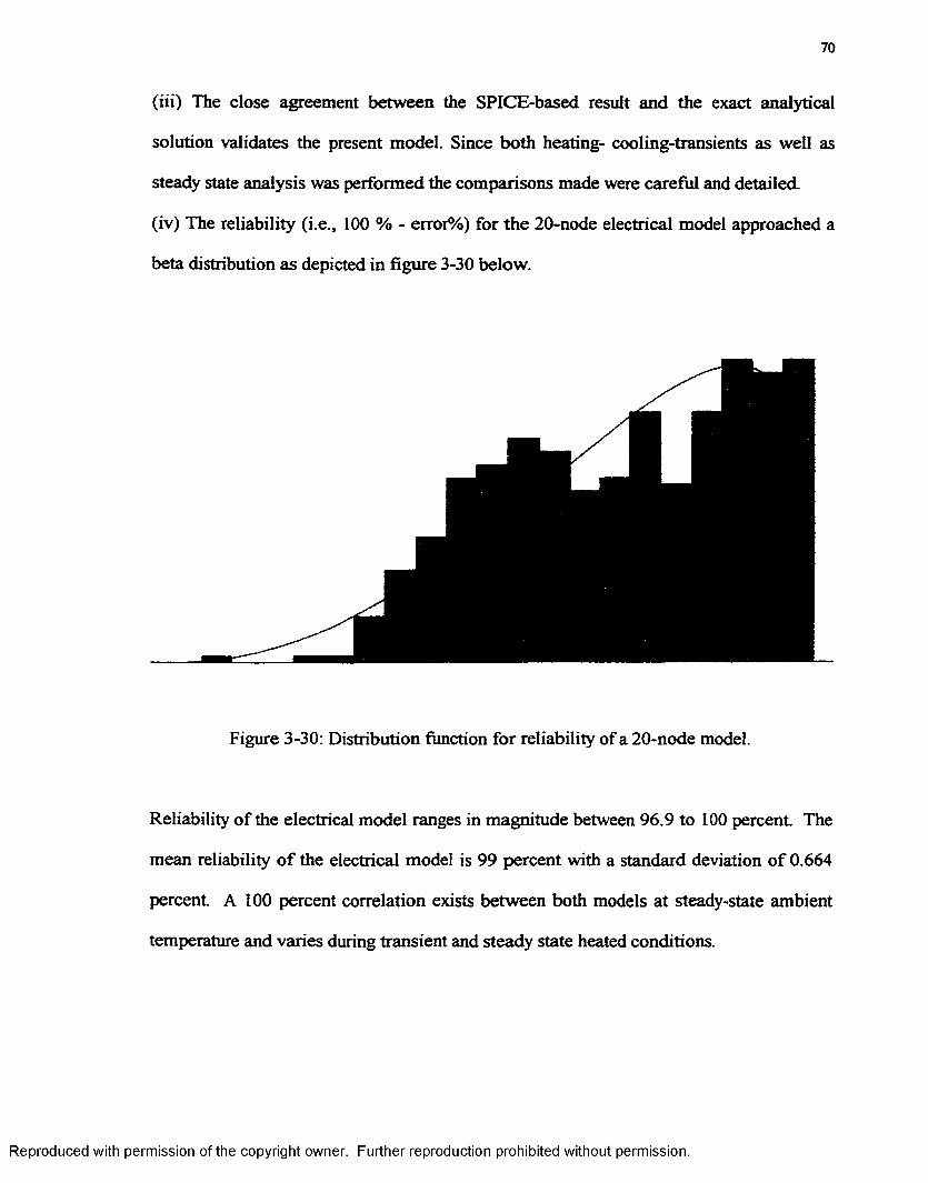
70
(iii) The close agreement between the SPICE-based result and the exact analytical
solution validates the present model. Since both heating- cooling-transients as well as
steady state analysis was performed the comparisons made were careful and detailed.
(iv) The reliability (i.e., 100 % - error%) for the 20-node electrical model approached a
beta distribution as depicted in figure 3-30 below.
Figure 3-30: Distribution function for reliability of a 20-node model.
Reliability o f the electrical model ranges in magnitude between 96.9 to 100 percent. The
mean reliability o f the electrical model is 99 percent with a standard deviation o f 0.664
percent. A 100 percent correlation exists between both models at steady-state ambient
temperature and varies during transient and steady state heated conditions.
Reproduced with permission of the copyright owner. Further reproduction prohibited without permission.
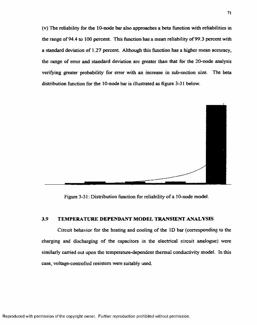
71
(v) The reliability for the 10-node bar also approaches a beta function with reliabilities in
the range o f 94.4 to 100 percent This function has a mean reliability o f 99.3 percent with
a standard deviation o f 1.27 percent. Although this function has a higher mean accuracy,
the range of error and standard deviation are greater than that for the 20-node analysis
verifying greater probability for error with an increase in sub-section size. The beta
distribution function for the 10-node bar is illustrated as figure 3-31 below.
Figure 3-31: Distribution function for reliability o f a 10-node model.
3.9 TEMPERATURE DEPENDANT MODEL TRANSIENT ANALYSIS
Circuit behavior for the heating and cooling o f the ID bar (corresponding to the
charging and discharging o f the capacitors in the electrical circuit analogue) were
similarly carried out upon the temperature-dependent thermal conductivity model. In this
case, voltage-controlled resistors were suitably used.
Reproduced with permission of the copyright owner. Further reproduction prohibited without permission.
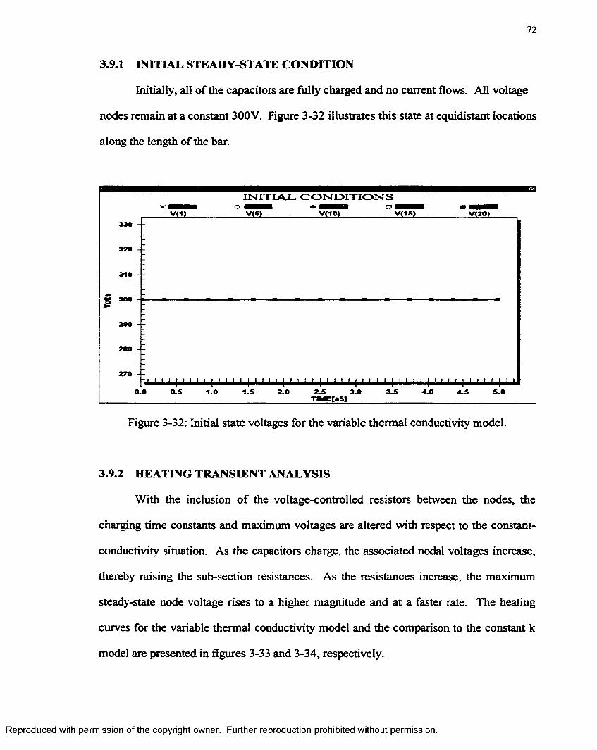
72
3.9.1 INITIAL STEADY-STATE CONDITION
Initially, all o f the capacitors are fully charged and no current flows. All voltage
nodes remain at a constant 300V. Figure 3-32 illustrates this state at equidistant locations
along the length o f the bar.
INITIAL CONDITIONS■ ■ ■ H • ■ ■ ■ Dv<s>____________v(-io)____________;
x o ■
330
320
310
280
270
0.0 0.5 1.5 2.0 3.0 3.5 4.0 5.01.0 4.5
Figure 3-32: Initial state voltages for the variable thermal conductivity model.
3.9.2 HEATING TRANSIENT ANALYSIS
With the inclusion o f the voltage-controlled resistors between the nodes, the
charging time constants and maximum voltages are altered with respect to the constant-
conductivity situation. As the capacitors charge, the associated nodal voltages increase,
thereby raising the sub-section resistances. As the resistances increase, the maximum
steady-state node voltage rises to a higher magnitude and at a faster rate. The heating
curves for the variable thermal conductivity model and the comparison to the constant k
model are presented in figures 3-33 and 3-34, respectively.
Reproduced with permission of the copyright owner. Further reproduction prohibited without permission.
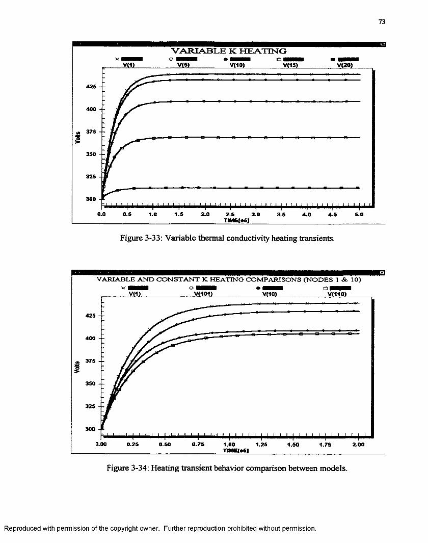
73
VARIABLE K HEATINGx ■■■■■ o ■■■■■ • q
VOI vgsi V(2p)
425 - -
400 - -
g> 375 - -
t350 - -
325
300
0.0 1.50.5 2.01.0 2.5 3.0 5.03.5 4.0 4.5TIMEIe51
Figure 3-33: Variable thermal conductivity heating transients.
V A R IA B L E A N D C O N S T A N T K H EA TIN G C O M P A R ISO N S (N O D E S 1 & 10)x ■■■■ o ■§■■■ m MBH
V(11 V(101) V(10> V(110)
425 - -
400 --
„ 375 - -aso:»
350 - -
325 - -
300
0.00 0.25 0.750.50 1.00 1.25 2.001.50 1.75_________________________________________________TIMEfrSl__________________________________________
Figure 3-34: Heating transient behavior comparison between models.
Reproduced with permission of the copyright owner. Further reproduction prohibited without permission.
74
The nodal voltages V (l) and V(10) correspond to nodes 1 and 10 o f the variable thermal
conductivity model. The constant thermal conductivity model depicts nodal voltages 1
and 10asV (101) and V(110), respectively, in Fig. 3-34. A comparison of the heating
curves in Figure 3-34 indicates that the variable thermal conductivity model reaches a
higher steady-state voltage than when it remained constant. This behavior corresponds to
the ideal expected analytical behavior. As the temperature within the bar rises, its
thermal conductivity decreases. With a decrease in thermal conductivity, heat travels
slower to the heat sink and builds up at the site. This buildup o f heat increases the
temperature at the location creating a more rapid heat up rate and a higher steady-state
temperature.
3.9.3 COOLING TRANSIENT ANALYSIS
Once the heat source is removed (current sources turned off) the capacitors begin
to discharge. As the capacitors discharge, the nodal voltages decrease. This decrease in
nodal voltage potential causes the sub-section resistors to also lower in value, causing the
capacitors to discharge faster. Even though the initial voltages at the nodes are higher for
the variable thermal conductivity model, it cools faster than the constant thermal
conductivity model due to the decreasing resistor values. Cooling curves for the variable
thermal conductivity model and the comparison to the constant k model are plotted in
figures 3-35 and 3-36, respectively.
Reproduced with permission of the copyright owner. Further reproduction prohibited without permission.
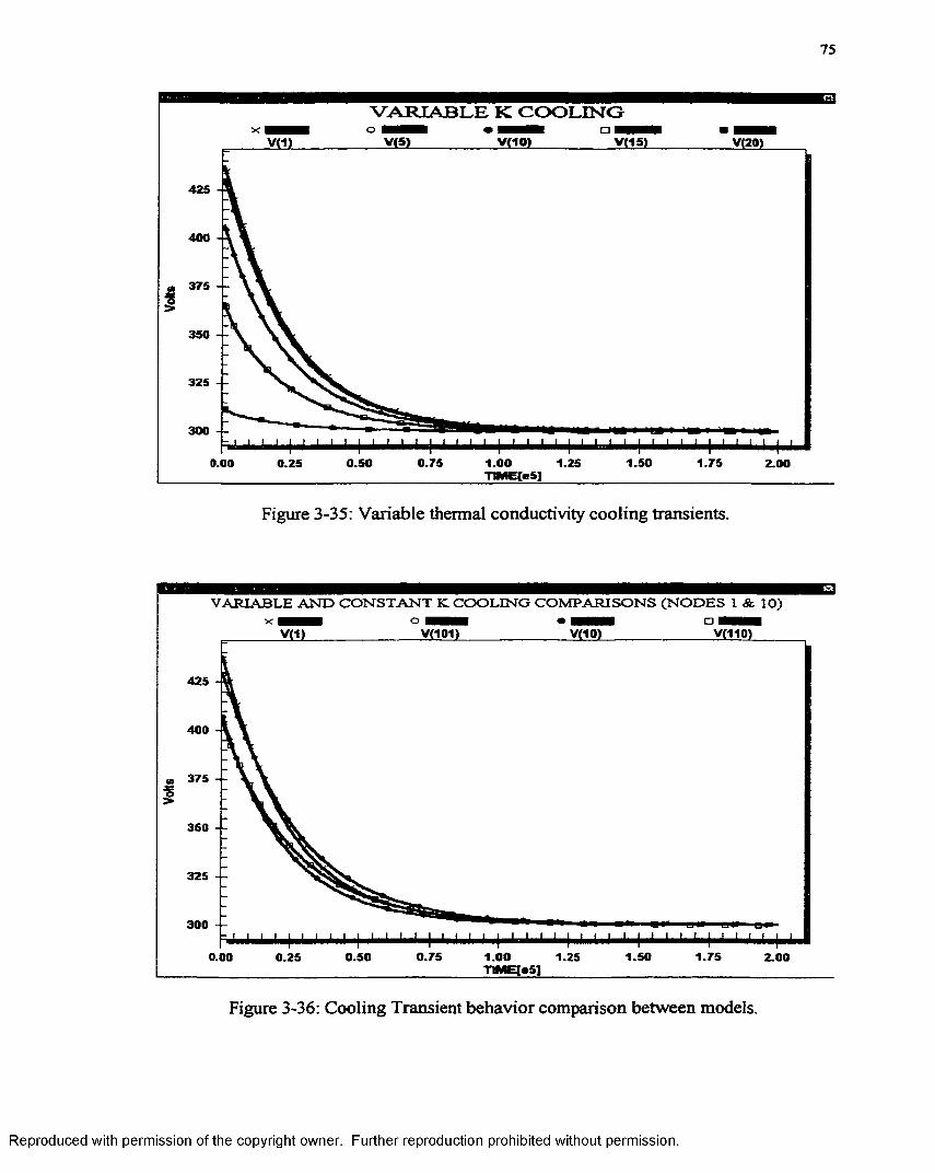
75
VARIABLE K COOLINGo ■■■■ • o M
i
V(5) VQQ) V(1S)
425
400
375
350
325
300
0.75 1.00 1.25 1.50 1.750.00 0.500.25 2.00TIME[eS]
Figure 3-35: Variable thermal conductivity cooling transients.
V A R IA B L E A N D C O N S T A N T K C O O L IN G C O M P A R IS O N S (N O D E S 1 & 10) x o ■ ■ ■ • ■■■■
V(101) yaioi
425
400
350
325
300
0.75 1.00 1.25 1.50 1.750.00 0.50 2.000.25TIMEtoSl
Figure 3-36: Cooling Transient behavior comparison between models.
Reproduced with permission of the copyright owner. Further reproduction prohibited without permission.
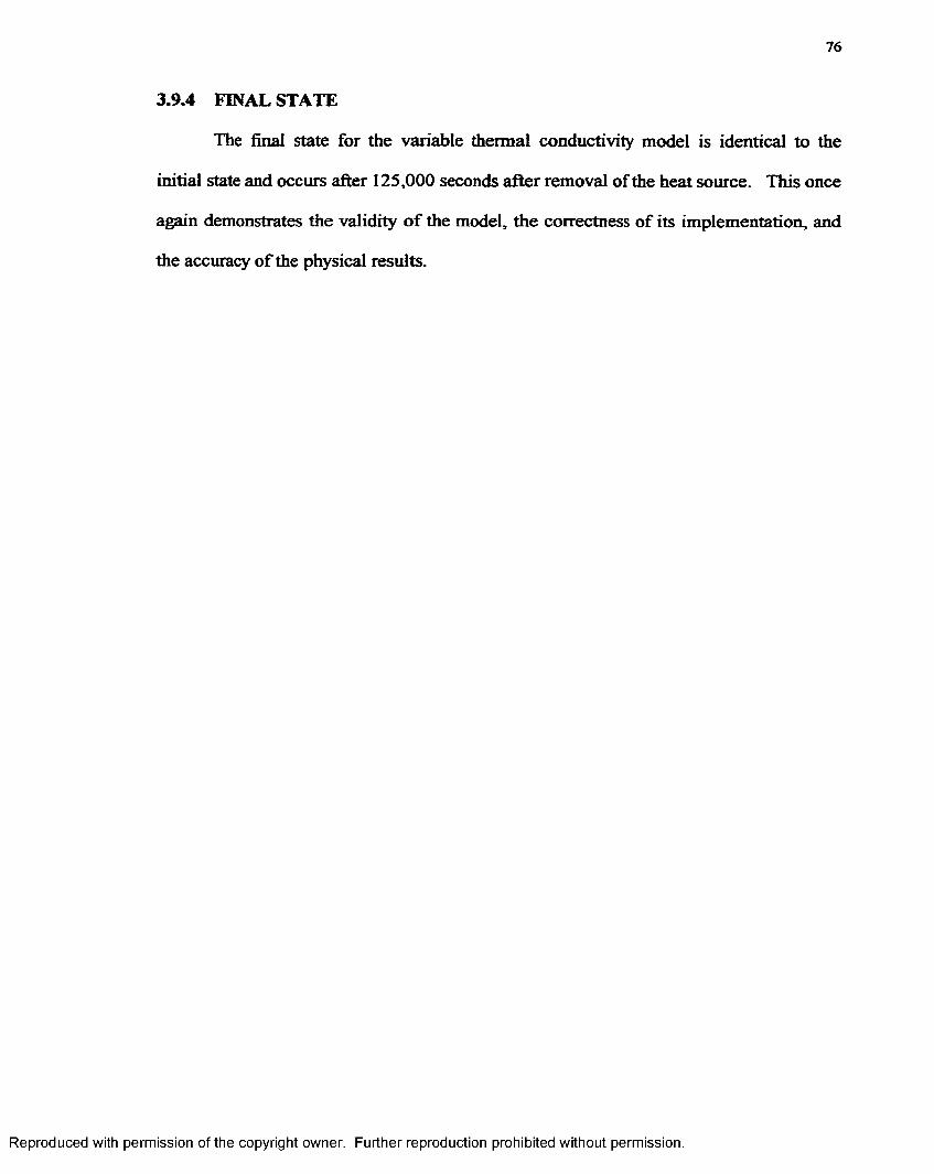
76
3.9.4 FINAL STATE
The final state for the variable thermal conductivity model is identical to the
initial state and occurs after 125,000 seconds after removal of the heat source. This once
again demonstrates the validity o f the model, the correctness o f its implementation, and
the accuracy o f the physical results.
Reproduced with permission of the copyright owner. Further reproduction prohibited without permission.
77
CHAPTER IV
RESULTS FOR THE THERMAL DIAGNOSTIC PROBLEM
4.1 INTRODUCTION
This chapter begins by introducing the possibility o f applying the SPICE-based
method for non-intrusive thermal diagnostic analysis. Non-intrusive thermal diagnostic
(NTTD) is a useful and increasingly popular tool to sense and detect material failures,
cracks, and structural imperfections. NITD is generally carried out by subjecting the
samples under test to pulsed thermal stimuli. Based on the signatures o f the transient
heating response within the sample, predictions can be made regarding its uniformity and
homogeneity. Deviations from expected behavior, in terms o f delays in the heat signal or
amplitude variations indicate damage or internal imperfections. In order to obtain quick
evaluations, it becomes desirable to scan the samples quickly, and yet obtain good spatial
resolution. This has become possible with the advent of pulsed lasers, which are being
used to locally heat sections o f the samples under test.
A case is made here for utilizing the current SPICE-based numerical technique to
accurately predict and model such heating transients and spatially resolved signatures for
NITD. The next section presents a brief discussion o f NITD. It is shown that NIDT will
require the analysis of transient heating and cooling curves at various sections of a
sample when it is subjected to external laser pulses to induce heating. Next, SPICE-based
results for the response o f a focused single and multiple traveling heat pulses are
presented for one-, two-, and three-dimensional cases. Initially, the transient behavior of
the traveling focused heat source is discussed and verified for a pure sample in the
absence o f any defects. Next, material defects are introduced to gauge the differences in
Reproduced with permission of the copyright owner. Further reproduction prohibited without permission.
78
the thermal transient signal. It is shown that the differences can be used to detect defects
and aberrations in homogeneity in samples through differential thermal analysis
simulations.
4.2 THERMAL DIAGNOSTICS - APPLICATIONS AND SCOPE
Nondestructive testing and diagnostics are beginning to play an increasingly
important role in reliability analysis, component wear-out testing, life-cycle estimates,
and safety inspections [36]. Critical areas o f nondestructive and non-intrusive testing for
safety include: crack detection in airplane structures (especially the wings), fatigue in
heavy machinery, and load-bearing rotating components and equipment. In general,
structural components subjected to cyclic and/or random loads can develop cracks [37],
Corrosion can accelerate this failure process. Once a crack initiates, it can grow during
subsequent load cycles leading to catastrophic failure and hazardous consequences.
Therefore, it is important to be able to detect such cracks, fractures, and stress-related
inhomogeneities for preventive maintenance. In this regard, a variety o f techniques have
been proposed for such monitoring and nonintrusive diagnostics [38-41]. These
techniques are required since it is not easy or practical to dismantle equipment during the
testing process, and care must be taken to ensure that no damage results in the diagnostic
procedure itself. The ever-increasing demand for early detection o f fatigue damage is
fueled by the fact that small cracks are found to grow at unexpectedly high rates well
below the “large-crack thresholds” in aluminum and titanium materials [42],
The detection of surface-breaking defects is important because stresses arising
from strain are often maximized at the structure surface so that any surface-breaking
Reproduced with permission of the copyright owner. Further reproduction prohibited without permission.

79
defect is particularly prone to growth. Significant work has already been devoted to the
detection, location, and sizing of surface-breaking defects [43]. Ultrasound is an
important method due to its convenience, reliability and efficient propagation in metals
[44, 45]. In this area, there are two main kinds of detection methods: (a) those based on
Rayleigh wave interaction with surface-breaking cracks [46-48], and (b) those based on
the time-of-flight diffraction (TOFD) technique [49-51]. The latter is also used to detect
subsurface defects by conventional ultrasound. The TOFD method uses the arrival time
of ultrasound diffracted from the tip o f the crack to determine the size o f the defect in a
through-thickness direction. It has the advantage that amplitude information from the
received signal is not employed directly for defect sizing, but instead, the time of arrival
o f the signal is used.
Positive identification of small fatigue cracks and material inhomogeneities,
presents a challenging problem since it is important to first distinguish them from the
primary geometric features and secondary irregularities (such as caused by uneven
machining, mechanical wear, and corrosion). Under laboratory conditions, a great
variety o f nondestructive evaluation techniques have been developed for detection of
defects and material characterization. These include: acoustic emission [52-54], linear
and non-linear ultrasonics [40, 43, 45], eddy-current inspection [55-57], x-ray imaging
[58], and thermal sensing [59, 60], Optical methods that include the use o f microscopes
and dye penetrants have also been used. However, the optical techniques are often not
well-suited either because the affected areas are not accessible, or the defect dimensions
are below the resolution limits o f the microscopes. Most recently, three new techniques,
namely, holographic interferometry, structural integrity monitoring, and laser ultrasound
Reproduced with permission of the copyright owner. Further reproduction prohibited without permission.
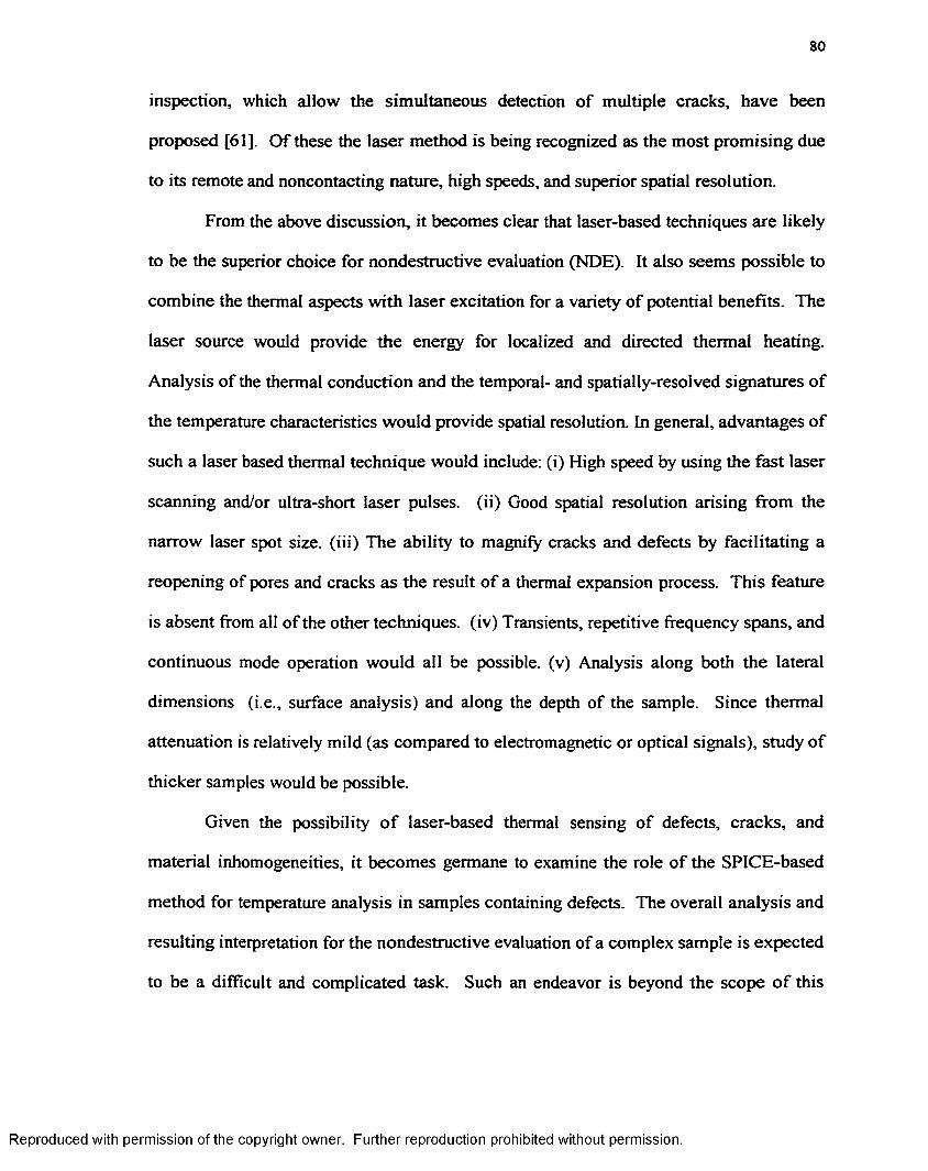
80
inspection, which allow the simultaneous detection of multiple cracks, have been
proposed [61], Of these the laser method is being recognized as the most promising due
to its remote and noncontacting nature, high speeds, and superior spatial resolution.
From the above discussion, it becomes clear that laser-based techniques are likely
to be the superior choice for nondestructive evaluation (NDE). It also seems possible to
combine the thermal aspects with laser excitation for a variety of potential benefits. The
laser source would provide the energy for localized and directed thermal heating.
Analysis of the thermal conduction and the temporal- and spatially-resolved signatures of
the temperature characteristics would provide spatial resolution. In general, advantages o f
such a laser based thermal technique would include: (i) High speed by using the fast laser
scanning and/or ultra-short laser pulses, (ii) Good spatial resolution arising from the
narrow laser spot size, (iii) The ability to magnify cracks and defects by facilitating a
reopening of pores and cracks as the result o f a thermal expansion process. This feature
is absent from all of the other techniques, (iv) Transients, repetitive frequency spans, and
continuous mode operation would all be possible, (v) Analysis along both the lateral
dimensions (i.e., surface analysis) and along the depth of the sample. Since thermal
attenuation is relatively mild (as compared to electromagnetic or optical signals), study of
thicker samples would be possible.
Given the possibility o f laser-based thermal sensing of defects, cracks, and
material inhomogeneities, it becomes germane to examine the role o f the SPICE-based
method for temperature analysis in samples containing defects. The overall analysis and
resulting interpretation for the nondestructive evaluation of a complex sample is expected
to be a difficult and complicated task. Such an endeavor is beyond the scope o f this
Reproduced with permission of the copyright owner. Further reproduction prohibited without permission.
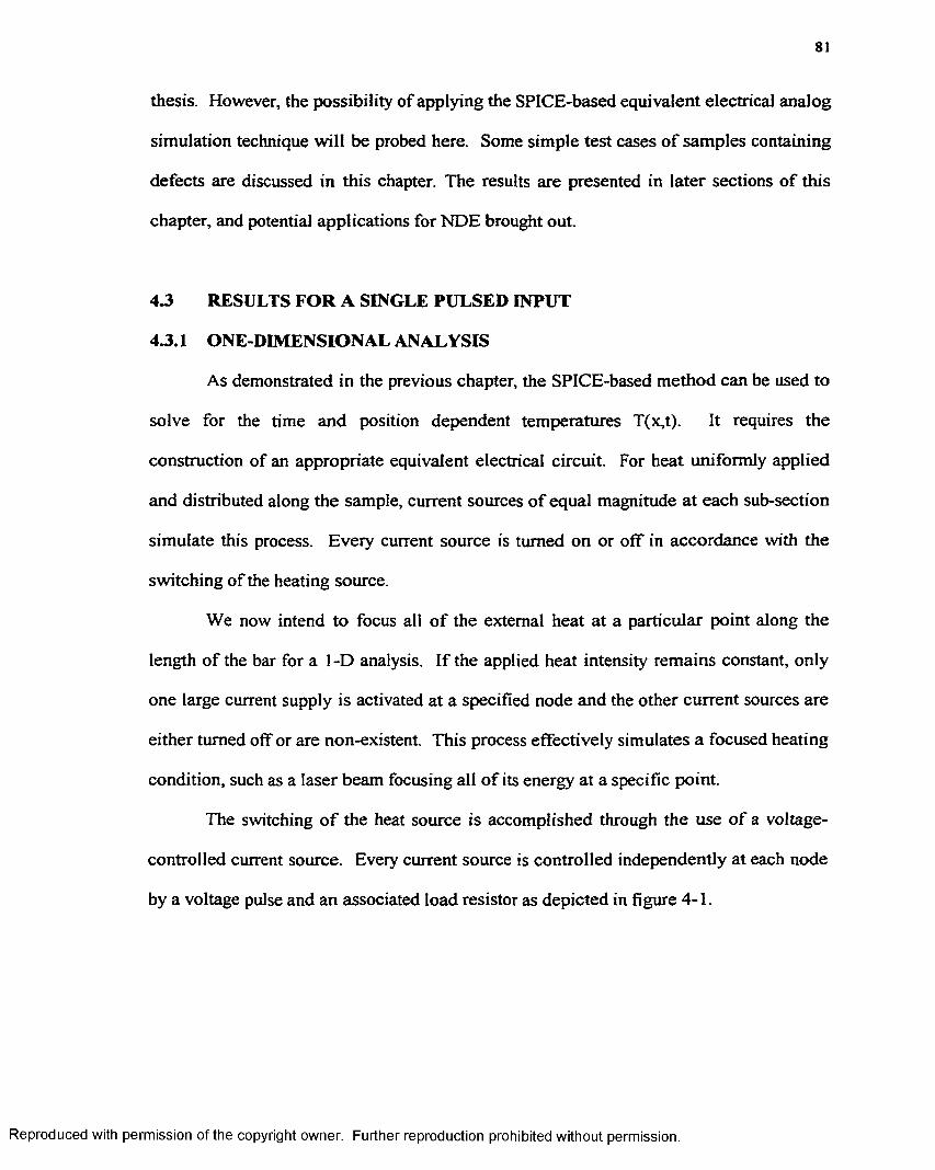
81
thesis. However, the possibility of applying the SPICE-based equivalent electrical analog
simulation technique will be probed here. Some simple test cases o f samples containing
defects are discussed in this chapter. The results are presented in later sections o f this
chapter, and potential applications for NDE brought out.
43 RESULTS FOR A SINGLE PULSED INPUT
43.1 ONE-DIMENSIONAL ANALYSIS
As demonstrated in the previous chapter, the SPICE-based method can be used to
solve for the time and position dependent temperatures T(x,t). It requires the
construction of an appropriate equivalent electrical circuit. For heat uniformly applied
and distributed along the sample, current sources o f equal magnitude at each sub-section
simulate this process. Every current source is tinned on or off in accordance with the
switching of the heating source.
We now intend to focus all o f the external heat at a particular point along the
length of the bar for a 1-D analysis. If the applied heat intensity remains constant, only
one large current supply is activated at a specified node and the other current sources are
either turned off or are non-existent. This process effectively simulates a focused heating
condition, such as a laser beam focusing all o f its energy at a specific point.
The switching o f the heat source is accomplished through the use o f a voltage-
controlled current source. Every current source is controlled independently at each node
by a voltage pulse and an associated load resistor as depicted in figure 4-1.
Reproduced with permission of the copyright owner. Further reproduction prohibited without permission.
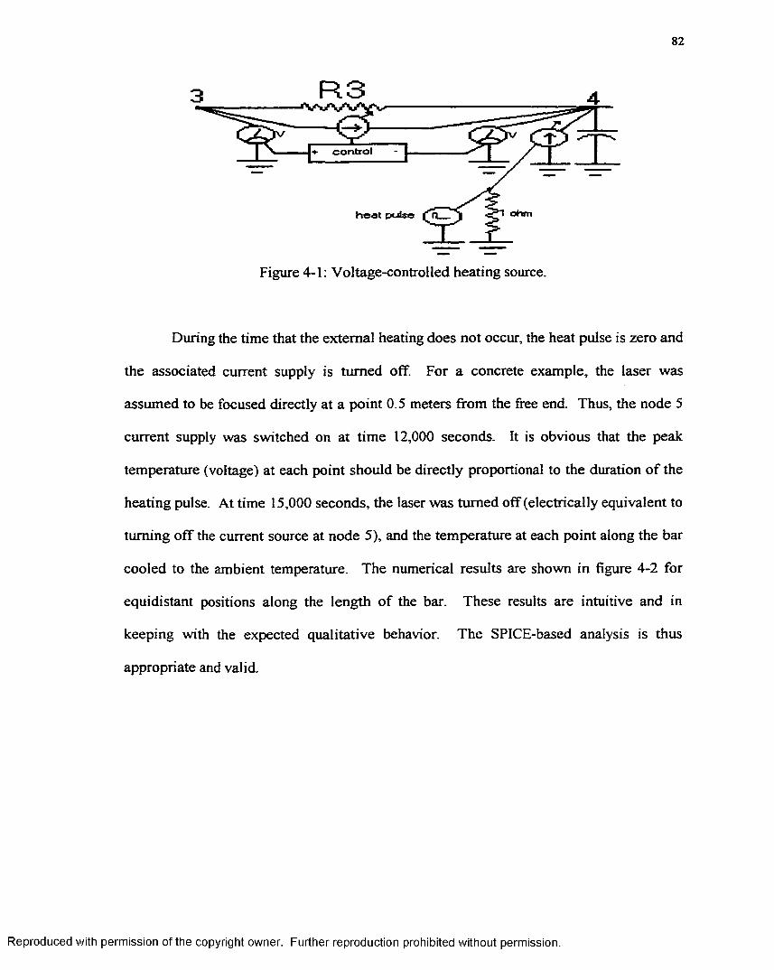
82
R 3
+ control
ohmheat pulse fn __
Figure 4-1: Voltage-controlled heating source.
During the time that the external heating does not occur, the heat pulse is zero and
the associated current supply is turned off. For a concrete example, the laser was
assumed to be focused directly at a point 0.5 meters from the free end. Thus, the node 5
current supply was switched on at time 12,000 seconds. It is obvious that the peak
temperature (voltage) at each point should be directly proportional to the duration o f the
heating pulse. At time 15,000 seconds, the laser was turned off (electrically equivalent to
turning off the current source at node 5), and the temperature at each point along the bar
cooled to the ambient temperature. The numerical results are shown in figure 4-2 for
equidistant positions along the length of the bar. These results are intuitive and in
keeping with the expected qualitative behavior. The SPICE-based analysis is thus
appropriate and valid.
Reproduced with permission of the copyright owner. Further reproduction prohibited without permission.
83
LASER ON SECTION 5 ■■■■ • ■■■■ □V<5)
xVMS) V(20)
335
330
325
a, 320
315
310
305
300
0.75 1-50 1.75 2.000.00 0.50 1.00TIMEteS]
1.250.25
Figure 4-2: Transient behavior of a heating pulse directed at node 5.
4.3.2 TWO-DIMENSIONAL (2-D) ANALYSIS
To test the transient results for a 2-D sample, the plane is first sectioned into nine
individual pieces as shown in figure 4-3.
e
►x
Figure 4-3: Separating the two-dimensional sample into individual sections.
Reproduced with permission of the copyright owner. Further reproduction prohibited without permission.
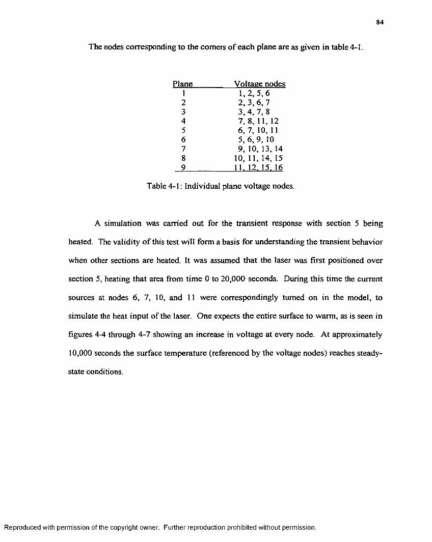
84
The nodes corresponding to the comers o f each plane are as given in table 4-1.
Plane Voltage nodes1 1,2 , 5 ,62 2, 3, 6, 7
3, 4, 7, 84 7, 8, 11, 125 6, 7, 10, 116 5, 6, 9, 107 9, 10, 13,148 10, 11, 14, 159 11. 12. 15. 16
Table 4-1: Individual plane voltage nodes.
A simulation was carried out for the transient response with section 5 being
heated. The validity o f this test will form a basis for understanding the transient behavior
when other sections are heated. It was assumed that the laser was first positioned over
section 5, heating that area from time 0 to 20,000 seconds. During this time the current
sources at nodes 6, 7, 10, and 11 were correspondingly turned on in the model, to
simulate the heat input of the laser. One expects the entire surface to warm, as is seen in
figures 4-4 through 4-7 showing an increase in voltage at every node. At approximately
10,000 seconds the surface temperature (referenced by the voltage nodes) reaches steady-
state conditions.
Reproduced with permission of the copyright owner. Further reproduction prohibited without permission.
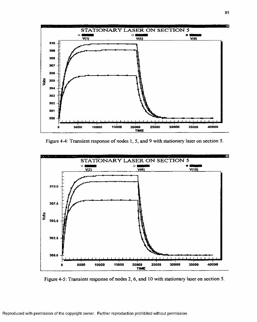
85
S T A T I O N A R Y L A S E R O N S E C T I O N 5x o
V(1) yxy310
309
308
307
306
303
302
301
300
4000015000 25000 30000 350005000 10000 200000TIME
Figure 4-4: Transient response o f nodes I, 5, and 9 with stationary laser on section 5.
S T A T I O N A R Y L A S E R O N S E C T I O N 5x o
V(10)V(2) V<6)
310.0
307.5
</>3£O>305.0
302.5
300.0
4000025000 30000 3500010000 150005000 200000TIME
Figure 4-5: Transient response o f nodes 2, 6, and 10 with stationary laser on section 5.
Reproduced with permission of the copyright owner. Further reproduction prohibited without permission.
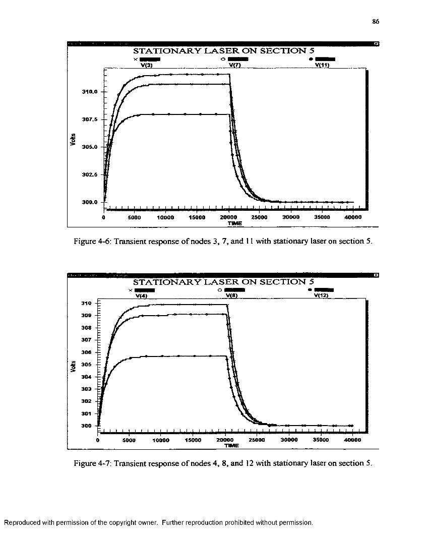
86
STATIONARY LASER ON SECTION 5'x ■■■■■ o ■ ■ ■ ! •
V(3)
310.0
307.5
aso305.0
302.5
300.0
30000 35000 4000020000 250000 150005000 10000TIME
Figure 4-6: Transient response o f nodes 3, 7, and 11 with stationary laser on section 5.
STATIONARY LASER ON SECTION 5X | O ■ ■ ■ ■
V(12)V<8)310
309
308
307
306
| 305
304
303
302
301
300
3500030000 4000020000 250000 150005000 10000TIME
Figure 4-7: Transient response o f nodes 4, 8, and 12 with stationary laser on section 5.
Reproduced with permission of the copyright owner. Further reproduction prohibited without permission.
87
A close inspection o f the voltages results reveals the following features: (i) The
greatest temperature difference occurs between the heat sink (voltage nodes 13 through
16) and the sub-section junctions adjacent to it (voltage nodes 9 through 12). This
situation occurs because the heat cumulates at each sub-section junction (voltage node) as
it flows towards the heat sink, (ii) A symmetry about the x-axis is evident. Since both x-
axis ends are insulated and are equal in distance (but opposite in direction) from the
heating point, temperature dissipates evenly in both directions causing equidistant points
to be at the same temperature, (iii) Finally, when adjacent sub-section junctions (voltage
nodes) are heated, the temperatures at both junctions along the x-axis are the same. This
situation occurs because there is an equal distance and thus equal heat dissipation along
the x-axis to the insulated ends. With both temperatures at the same magnitude, no
temperature difference occurs between the junctions causing the heat to remain stationary
between those points.
These statements are summarized by the following set o f equations:
V l = V4, AV2, l = A V 3,4 (4.1)V5 = V8, AV6, 5 = AV7, 8 (4.2)V9 = V l2 , AVlO, 9 = A Vl 1, 12 (4.3)V2 = V3, V6 = V7, VlO = V l 1 (4.4)AV9, 13 > AV5, 9 > A V l, 5 (4.5)A V 10, 14 > AV6, 10 > AV2, 6 (4.6)AV 11, 15 > AV7, 11 > AV3, 7 (4.7)A V l2, 16 > AV8, 12 > AV4, 8 (4.8)
Equations (4-1) through (4-3) verify equal heat dissipation along the x-axis. No heat
flow due to equal temperatures between adjacent junctions is verified by equation (4-4).
Finally, equations (4-5) through (4-8) represent heat flowing down the y-axis to the heat
sink. At time 20,000 seconds, the heat source was removed and the entire surface began
to cool. The cooling continues following the conditions of equations (4-1X4-8) until the
Reproduced with permission of the copyright owner. Further reproduction prohibited without permission.
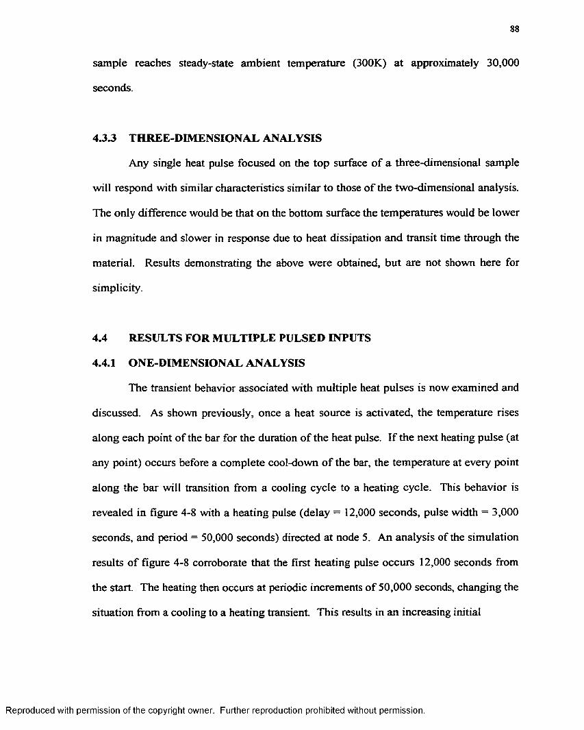
88
sample reaches steady-state ambient temperature (300K) at approximately 30,000
seconds.
4.3.3 THREE-DIMENSIONAL ANALYSIS
Any single heat pulse focused on the top surface o f a three-dimensional sample
will respond with similar characteristics similar to those o f the two-dimensional analysis.
The only difference would be that on the bottom surface the temperatures would be lower
in magnitude and slower in response due to heat dissipation and transit time through the
material. Results demonstrating the above were obtained, but are not shown here for
simplicity.
4.4 RESULTS FOR MULTIPLE PULSED INPUTS
4.4.1 ONE-DIMENSIONAL ANALYSIS
The transient behavior associated with multiple heat pulses is now examined and
discussed. As shown previously, once a heat source is activated, the temperature rises
along each point of the bar for the duration o f the heat pulse. If the next heating pulse (at
any point) occurs before a complete cool-down o f the bar, the temperature at every point
along the bar will transition from a cooling cycle to a heating cycle. This behavior is
revealed in figure 4-8 with a heating pulse (delay = 12,000 seconds, pulse width = 3,000
seconds, and period = 50,000 seconds) directed at node 5. An analysis of the simulation
results o f figure 4-8 corroborate that the first heating pulse occurs 12,000 seconds from
the start. The heating then occurs at periodic increments o f 50,000 seconds, changing the
situation from a cooling to a heating transient. This results in an increasing initial
Reproduced with permission of the copyright owner. Further reproduction prohibited without permission.
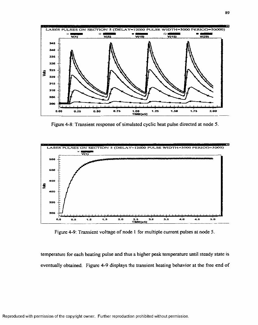
89
LASER PULSES ON SECTION 5 (DELAY-12000 PULSE W ID TH -3000 PERIOD-SOOOO) x ■■■■ o □ BHBB ■ BHBHi
V<5)
345
335
330
325
320
315
310
305
300
Z.OO0.00 0.75 1.25 1.50 1.750.50 1.000.25TIME[cS]
Figure 4-8: Transient response o f simulated cyclic heat pulse directed at node 5.
LASER PULSES ON SECTION S (DELAY= 12000 PULSE WIDTH*3000 PERIOD—5000)
560
500
400
350
300
2.0 5.00.0 1.00.5
Figure 4-9: Transient voltage o f node l for multiple current pulses at node 5.
temperature for each heating pulse and thus a higher peak temperature until steady state is
eventually obtained. Figure 4-9 displays the transient heating behavior at the free end of
Reproduced with permission of the copyright owner. Further reproduction prohibited without permission.
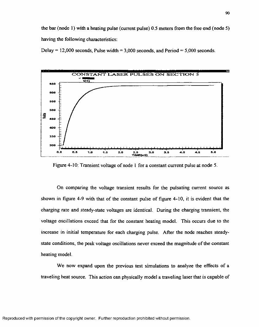
90
the bar (node 1) with a heating pulse (current pulse) 0.5 meters from the free end (node 5)
having the following characteristics:
Delay = 12,000 seconds, Pulse width = 3,000 seconds, and Period = 5,000 seconds.
CONSTANT LASER PULSES ON SECTION 5
550
500
I 450
400
350
300
0.0 0.5 5.01.0 3.0 4.61.5 2.5 3.5TIMEteSl
Figure 4-I0: Transient voltage of node I for a constant current pulse at node 5.
On comparing the voltage transient results for the pulsating current source as
shown in figure 4-9 with that of the constant pulse of figure 4-I0, it is evident that the
charging rate and steady-state voltages are identical. During the charging transient, the
voltage oscillations exceed that for the constant heating model. This occurs due to the
increase in initial temperature for each charging pulse. After the node reaches steady-
state conditions, the peak voltage oscillations never exceed the magnitude of the constant
heating model.
We now expand upon the previous test simulations to analyze the effects of a
traveling heat source. This action can physically model a traveling laser that is capable of
Reproduced with permission of the copyright owner. Further reproduction prohibited without permission.
91
localized heating within a given spot size, moving along the length o f a 1-D bar from the
location x = 0 to x = L. At each sub-section junction the laser remains stationary for
3,000 seconds applying heat to that specific point. It is then taken to travel to the next
junction. This process is electrically equivalent to activating a current source at the
corresponding node for 3,000 seconds and then turning it off while simultaneously
activating the next succeeding current source, and so on.
This procedure incorporates characteristics o f both focused single and multiple
heating pulses. As witnessed earlier, activating a current source at any node causes the
voltage to rise at every point along the bar. Once the current source is turned off at a
particular node, the capacitor begins to discharge causing the nodal voltage to lower
(simulating the cooling o f the sub-section junction). But this cooling action is of
extremely short duration because, once the adjacent current source is activated, the same
node begins to charge again. As we continue this simulated heating process down the
length o f the bar, the effects of distant heating pulses contribute a smaller effect on the
change in temperature at the prior heating points. Hence, eventually the nodes all begin
to cool.
This process is now analyzed in detail for a 2-meter, 20 sub-section bar. The laser
begins at x = 0 (node 1) at t = 0 and heats (i.e., turns on the node 1 current supply) the
point for 3,000 seconds. Heating at this point then ceases (the node 1 current supply is
turned off), and the laser moves to the next sub-section junction at x = 0.1m (node 2).
This section begins its heating cycle at time 3,000 seconds and remains at this point for
an additional 3,000 seconds heating the bar at x = 0.1m. This action is simulated
electronically by activating the current source at node 2 from time 3,000 to 6,000 seconds
Reproduced with permission of the copyright owner. Further reproduction prohibited without permission.
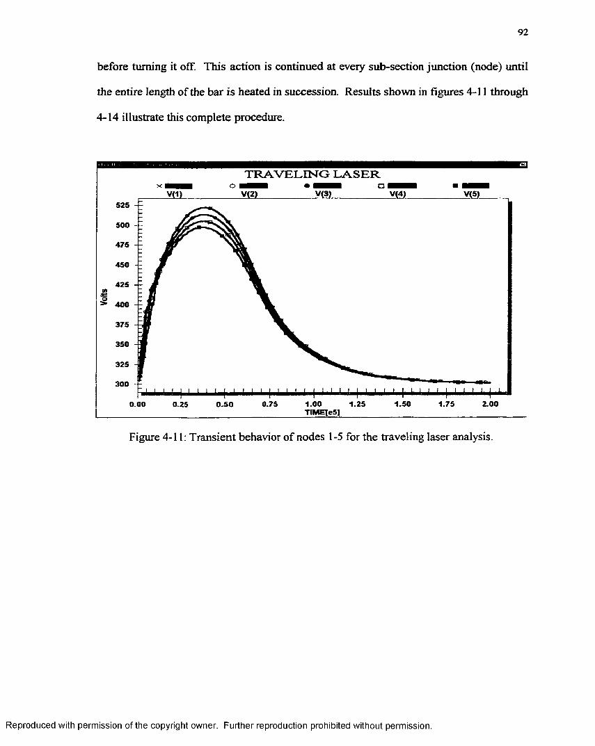
92
before turning it off. This action is continued at every sub-section junction (node) until
the entire length of the bar is heated in succession. Results shown in figures 4-11 through
4-14 illustrate this complete procedure.
T R A V E L IN G L A S E RX
V(4)V(1)525
500
475
450
425
:> 400
375
350
325
300
1.25 1.50 1.75 2.000.750.00 0.25 0.50
Figure 4-11: Transient behavior o f nodes 1-5 for the traveling laser analysis.
Reproduced with permission of the copyright owner. Further reproduction prohibited without permission.
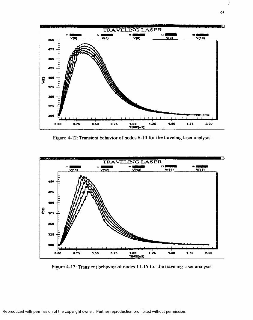
93
1 3TRAVELING LASER
x- BBBB o ^BHBi • ^B^B □ B B B ■ ■■■■V(8)______________ V<7)______________ V<8)_______________V(9)_____________ V<10)
' L ' J ( ‘ | ' ' ' ' | '0.00 0.25 0.50 0.75 1.00 1.25 1.50 1.75 2.00____________________________________________TIMEtcS]________________________________________
Figure 4-12: Transient behavior o f nodes 6-10 for the traveling laser analysis.
TRAVELING LASER
V(11) V(12>
450
425
400
> 375
350
325
300
1.501.25 1.75 2.001.000.00 0.50 0.750.25TIME[eSl
Figure 4-13: Transient behavior o f nodes 11-15 for the traveling laser analysis.
Reproduced with permission of the copyright owner. Further reproduction prohibited without permission.
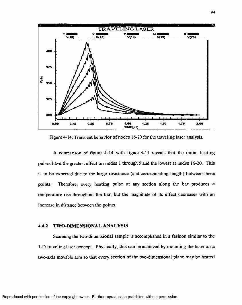
94
TRAVELING LASERV
V(20)
400
375
350
325
300
0.750.00 1.25 1.50 1.75 2.000.500.25
Figure 4-14: Transient behavior o f nodes 16-20 for the traveling laser analysis.
A comparison of figure 4-14 with figure 4-11 reveals that the initial heating
pulses have the greatest effect on nodes 1 through 5 and the lowest at nodes 16-20. This
is to be expected due to the large resistance (and corresponding length) between these
points. Therefore, every heating pulse at any section along the bar produces a
temperature rise throughout the bar, but the magnitude of its effect decreases with an
increase in distance between the points.
4.4.2 TWO-DIMENSIONAL ANALYSIS
Scanning the two-dimensional sample is accomplished in a fashion similar to the
1-D traveling laser concept. Physically, this can be achieved by mounting the laser on a
two-axis movable arm so that every section o f the two-dimensional plane may be heated
Reproduced with permission of the copyright owner. Further reproduction prohibited without permission.
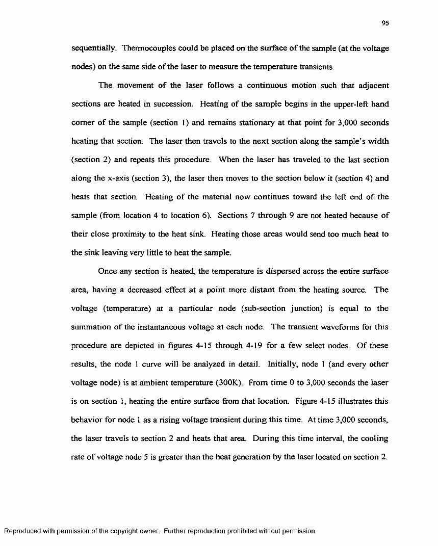
95
sequentially. Thermocouples could be placed on the surface o f the sample (at the voltage
nodes) on the same side o f the laser to measure the temperature transients.
The movement o f the laser follows a continuous motion such that adjacent
sections are heated in succession. Heating of the sample begins in the upper-left hand
comer o f the sample (section 1) and remains stationary at that point for 3,000 seconds
heating that section. The laser then travels to the next section along the sample’s width
(section 2) and repeats this procedure. When the laser has traveled to the last section
along the x-axis (section 3), the laser then moves to the section below it (section 4) and
heats that section. Heating o f the material now continues toward the left end of the
sample (from location 4 to location 6). Sections 7 through 9 are not heated because o f
their close proximity to the heat sink. Heating those areas would send too much heat to
the sink leaving very little to heat the sample.
Once any section is heated, the temperature is dispersed across the entire surface
area, having a decreased effect at a point more distant from the heating source. The
voltage (temperature) at a particular node (sub-section junction) is equal to the
summation o f the instantaneous voltage at each node. The transient waveforms for this
procedure are depicted in figures 4-15 through 4-19 for a few select nodes. O f these
results, the node 1 curve will be analyzed in detail. Initially, node 1 (and every other
voltage node) is at ambient temperature (300K). From time 0 to 3,000 seconds the laser
is on section 1, heating the entire surface from that location. Figure 4-15 illustrates this
behavior for node 1 as a rising voltage transient during this time. At time 3,000 seconds,
the laser travels to section 2 and heats that area. During this time interval, the cooling
rate o f voltage node 5 is greater than the heat generation by the laser located on section 2.
Reproduced with permission of the copyright owner. Further reproduction prohibited without permission.
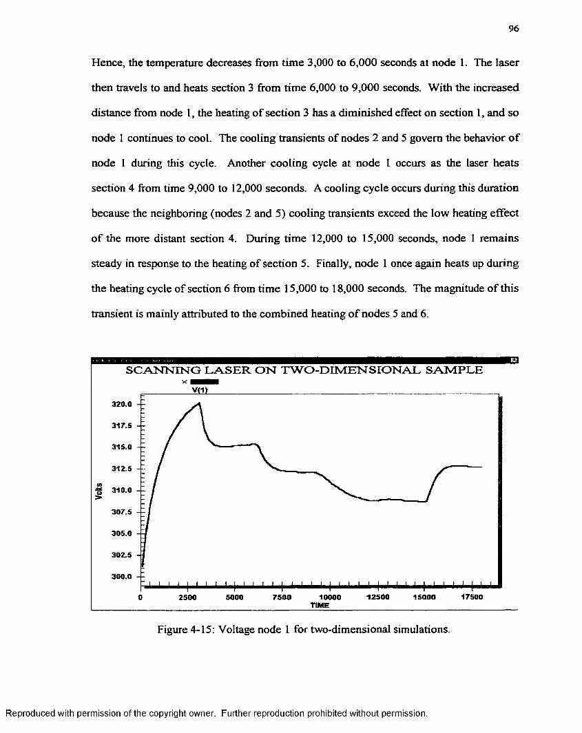
96
Hence, the temperature decreases from time 3,000 to 6,000 seconds at node 1. The laser
then travels to and heats section 3 from time 6,000 to 9,000 seconds. With the increased
distance from node I, the heating o f section 3 has a diminished effect on section 1, and so
node 1 continues to cool. The cooling transients of nodes 2 and 5 govern the behavior o f
node 1 during this cycle. Another cooling cycle at node 1 occurs as the laser heats
section 4 from time 9,000 to 12,000 seconds. A cooling cycle occurs during this duration
because the neighboring (nodes 2 and 5) cooling transients exceed the low heating effect
o f the more distant section 4. During time 12,000 to 15,000 seconds, node 1 remains
steady in response to the heating o f section 5. Finally, node 1 once again heats up during
the heating cycle of section 6 from time 15,000 to 18,000 seconds. The magnitude o f this
transient is mainly attributed to the combined heating o f nodes 5 and 6.
SCANNING LASER ON TWO-DIMENSIONAL SAMPLE
v(i)320.0
317.5
315.0
312.5
310.0
307.5
305.0
302.5
300.0
12500 17500150000 5000 7500 100002500TIME
Figure 4-15: Voltage node 1 for two-dimensional simulations.
Reproduced with permission of the copyright owner. Further reproduction prohibited without permission.
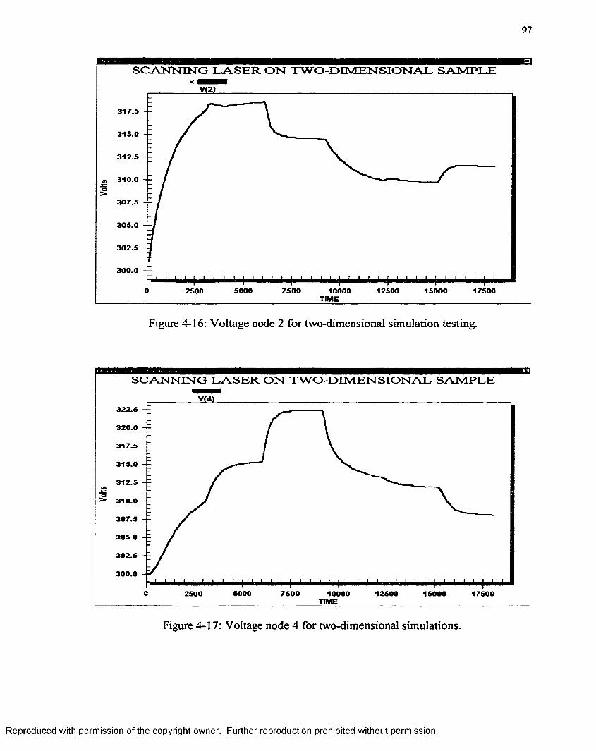
97
SCANNING LASER ON TWO-DIMENSIONAL SAMPLE
V(2)
317.5
315.0
312.5
310.0<n
I307.5
305.0
302.5
300.0
50000 75002500 12500 15000 1750010000TIME
Figure 4-16: Voltage node 2 for two-dimensional simulation testing.
SCANNING LASER ON TWO-DIMENSIONAL SAMPLE
VC4)322.5
320.0
317.5
315.0
312.5
>• 310.0
307.5
305.0
302.5
300.0
0 5000 7500 125002500 10000 15000 17500TIME
Figure 4-17: Voltage node 4 for two-dimensional simulations.
Reproduced with permission of the copyright owner. Further reproduction prohibited without permission.
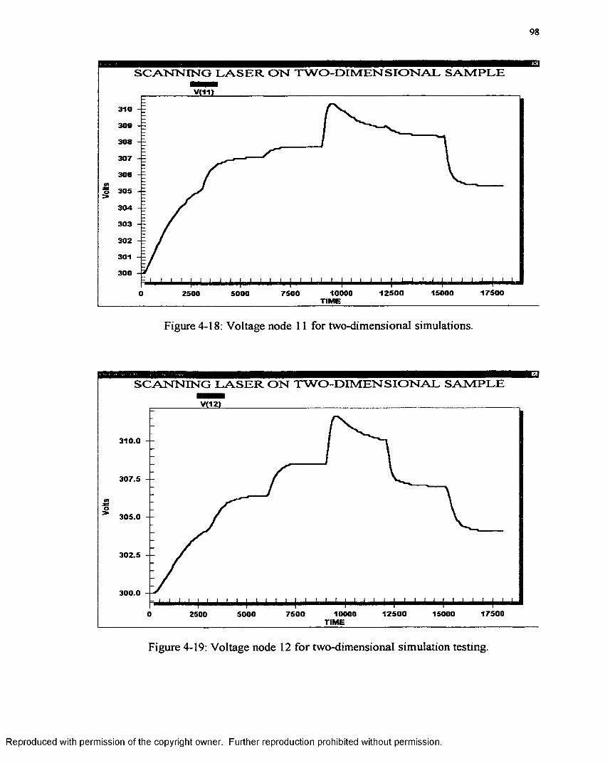
98
SCANNING LASER ON TWO-DIMENSIONAL SAMPLE
V(1D310
309
308
307
306a tm5 305
304
303
302
301
300
175001250010 0 0 0 1500075000 2500 5000TIME
Figure 4-18: Voltage node 11 for two-dimensional simulations.
SCANNING LASER ON TWO-DIMENSIONAL SAMPLEE3
310.0
307.5
305.0
302.5
300.0
1750012500 15000100000 2500 5000 7500TIME
Figure 4-19: Voltage node 12 for two-dimensional simulation testing.
Reproduced with permission of the copyright owner. Further reproduction prohibited without permission.
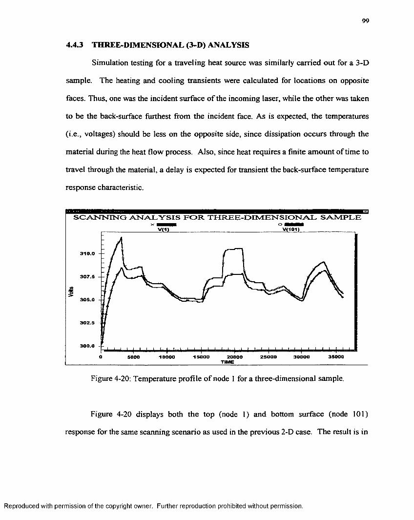
99
4 .43 THREE-DIMENSIONAL (3-D) ANALYSIS
Simulation testing for a traveling heat source was similarly carried out for a 3-D
sample. The heating and cooling transients were calculated for locations on opposite
faces. Thus, one was the incident surface o f the incoming laser, while the other was taken
to be the back-surface furthest from the incident face. As is expected, the temperatures
(i.e., voltages) should be less on the opposite side, since dissipation occurs through the
material during the heat flow process. Also, since heat requires a finite amount of time to
travel through the material, a delay is expected for transient the back-surface temperature
response characteristic.
SCANNING ANALYSIS FOR THREE-DIMENSIONAL SAMPLEX o H i
_______________________V(1)_________________________________________________V(101)________________________
310.0
307.5
305.0
302.5
300.0
3500020000TIME
25000 300005000
Figure 4-20: Temperature profile o f node 1 for a three-dimensional sample.
Figure 4-20 displays both the top (node 1) and bottom surface (node 101)
response for the same scanning scenario as used in the previous 2-D case. The result is in
Reproduced with permission of the copyright owner. Further reproduction prohibited without permission.
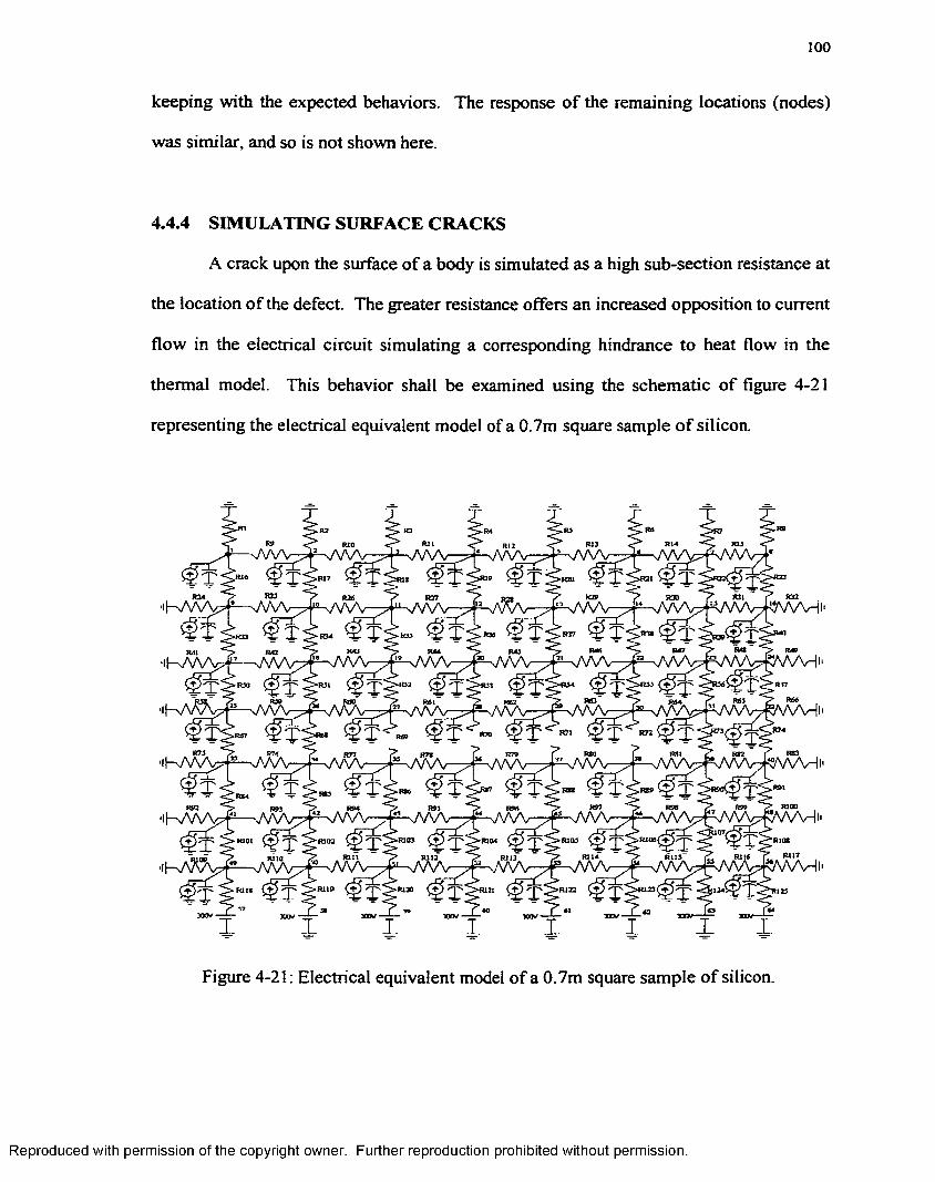
100
keeping with the expected behaviors. The response o f the remaining locations (nodes)
was similar, and so is not shown here.
4.4.4 SIMULATING SURFACE CRACKS
A crack upon the surface of a body is simulated as a high sub-section resistance at
the location of the defect. The greater resistance offers an increased opposition to current
flow in the electrical circuit simulating a corresponding hindrance to heat flow in the
thermal model. This behavior shall be examined using the schematic o f figure 4-21
representing the electrical equivalent model of a 0.7m square sample o f silicon.
RIO < - " R 2I < T R J2 < " KJ3
W W >4? -TVW J t
KA S K// f R2* f I® f7V W —^r-V vV v—t t V W V —T N V V V / f
R 34 7 r a j
ihTW V f
i h AVU2— ' 7VW
rod" ” Rfil” “ RO* ~s N V \ y ■ J r w v \ / - ^ vAAA/ ^ 4 ^nAAA/
R73 .7 R7« f j j R71 P R79 P RSO
lh A /W T f-N M A rT K /W V- > r v/WV—^nAAA/—^^-vAWv v ~ 7 —i/v v v -? —vvv v—^ T <
WVHii i - a w p —T w w p -w v v v w v - T f - m a - a wK101
r> I no ✓ KlllI ✓ l\J 41 ✓ i u u ✓ IUIJ n . • - R115
Figure 4-21: Electrical equivalent model of a 0.7m square sample o f silicon.
Reproduced with permission of the copyright owner. Further reproduction prohibited without permission.
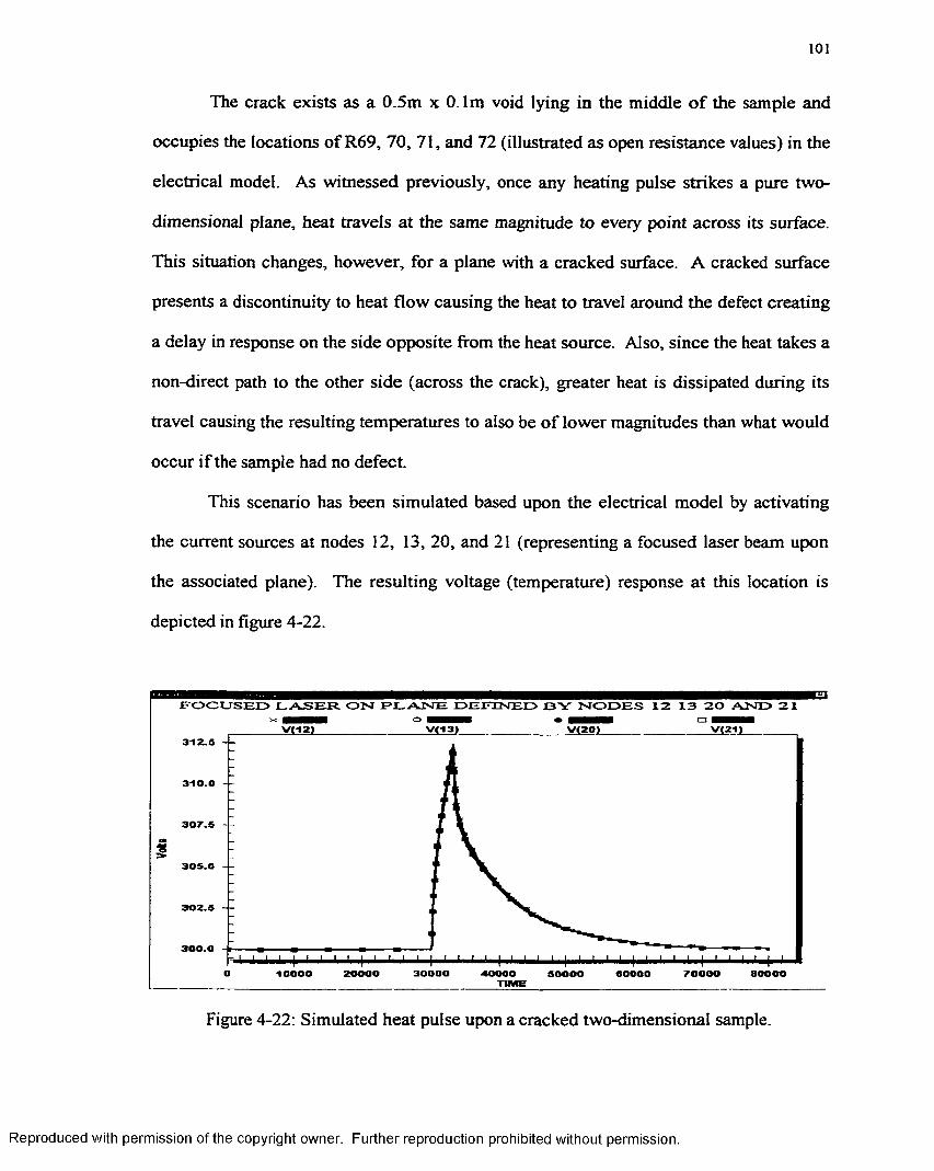
101
The crack exists as a 0.5m x 0.1m void lying in the middle o f the sample and
occupies the locations of R69, 70, 71, and 72 (illustrated as open resistance values) in the
electrical model. As witnessed previously, once any heating pulse strikes a pure two-
dimensional plane, heat travels at the same magnitude to every point across its surface.
This situation changes, however, for a plane with a cracked surface. A cracked surface
presents a discontinuity to heat flow causing the heat to travel around the defect creating
a delay in response on the side opposite from the heat source. Also, since the heat takes a
non-direct path to the other side (across the crack), greater heat is dissipated during its
travel causing the resulting temperatures to also be o f lower magnitudes than what would
occur if the sample had no defect.
This scenario has been simulated based upon the electrical model by activating
the current sources at nodes 12, 13, 20, and 21 (representing a focused laser beam upon
the associated plane). The resulting voltage (temperature) response at this location is
depicted in figure 4-22.
FOCUSED LASER ON PLANE DEFINED BY NODES 12 13 20 AND 21x MEBBi o EEiBBB • o
307.5
305.0
302.5
300.0
30000 40000TIME
70000 8000020000 50000 OOOOO
Figure 4-22: Simulated heat pulse upon a cracked two-dimensional sample.
Reproduced with permission of the copyright owner. Further reproduction prohibited without permission.
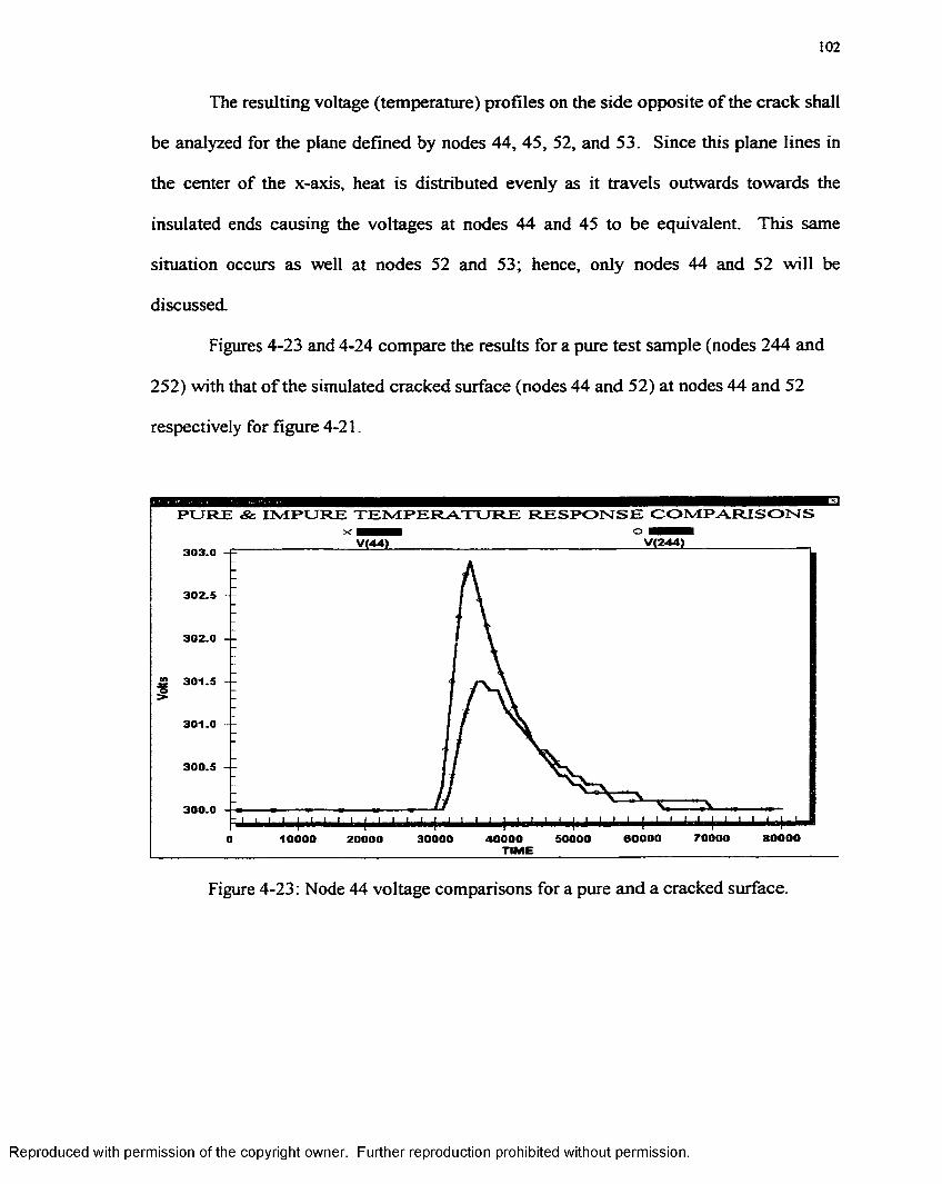
102
The resulting voltage (temperature) profiles on the side opposite o f the crack shall
be analyzed for the plane defined by nodes 44, 45, 52, and 53. Since this plane lines in
the center of the x-axis, heat is distributed evenly as it travels outwards towards the
insulated ends causing the voltages at nodes 44 and 45 to be equivalent. This same
situation occurs as well at nodes 52 and 53; hence, only nodes 44 and 52 will be
discussed.
Figures 4-23 and 4-24 compare the results for a pure test sample (nodes 244 and
252) with that o f the simulated cracked surface (nodes 44 and 52) at nodes 44 and 52
respectively for figure 4-21.
PURE & IMPURE TEMPERATURE RESPONSE COMPARISONS
V(244)V(44)
302.0
0 10000 20000 30000 40000 50000 60000 70000 80000TIME _________ ______
Figure 4-23: Node 44 voltage comparisons for a pure and a cracked surface.
Reproduced with permission of the copyright owner. Further reproduction prohibited without permission.
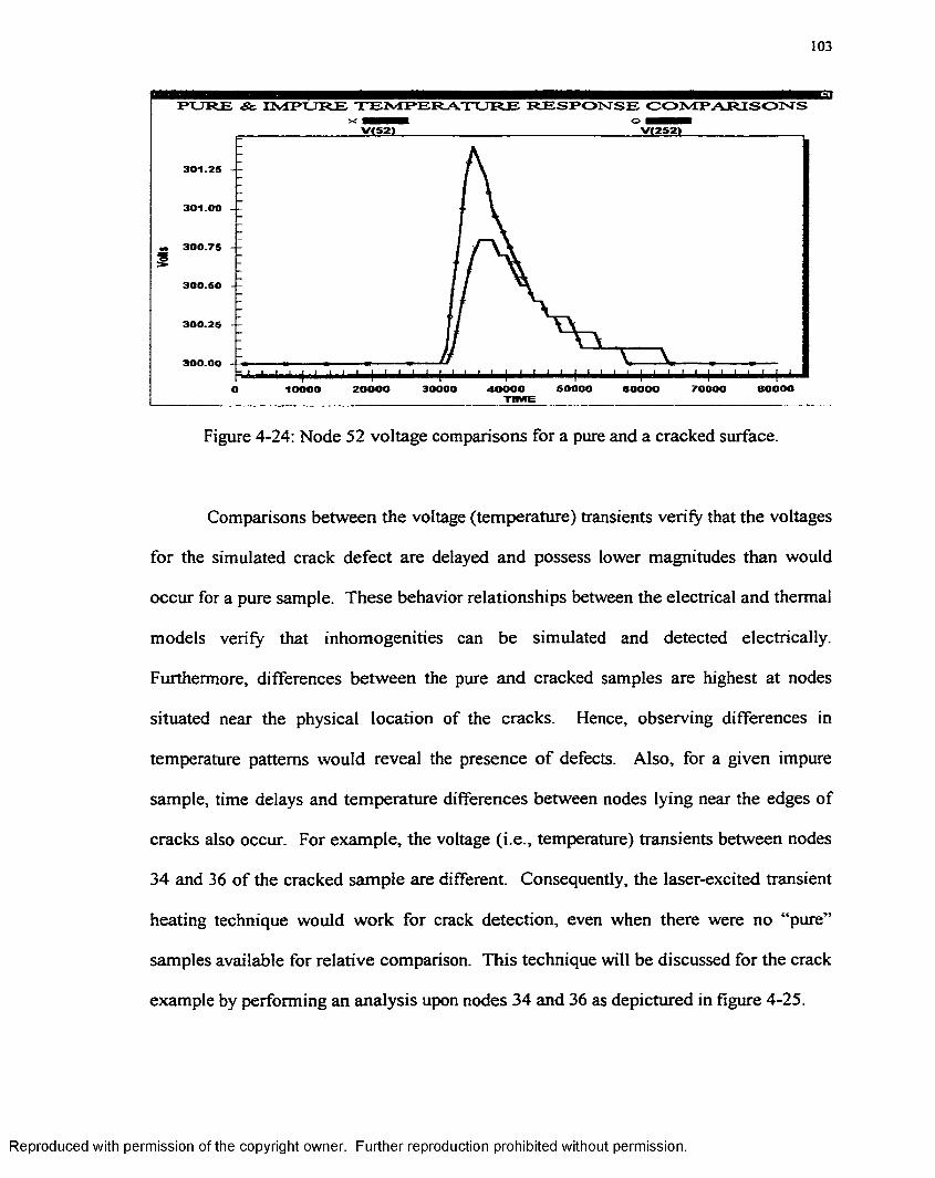
103
301.25
300.75
300.50
300.25
300.00
50000 70000 8000020000 30000 40000T IM E
6000010000
Figure 4-24: Node 52 voltage comparisons for a pure and a cracked surface.
Comparisons between the voltage (temperature) transients verify that the voltages
for the simulated crack defect are delayed and possess lower magnitudes than would
occur for a pure sample. These behavior relationships between the electrical and thermal
models verify that inhomogenities can be simulated and detected electrically.
Furthermore, differences between the pure and cracked samples are highest at nodes
situated near the physical location of the cracks. Hence, observing differences in
temperature patterns would reveal the presence o f defects. Also, for a given impure
sample, time delays and temperature differences between nodes lying near the edges of
cracks also occur. For example, the voltage (i.e., temperature) transients between nodes
34 and 36 of the cracked sample are different. Consequently, the laser-excited transient
heating technique would work for crack detection, even when there were no “pure”
samples available for relative comparison. This technique will be discussed for the crack
example by performing an analysis upon nodes 34 and 36 as depictured in figure 4-25.
Reproduced with permission of the copyright owner. Further reproduction prohibited without permission.
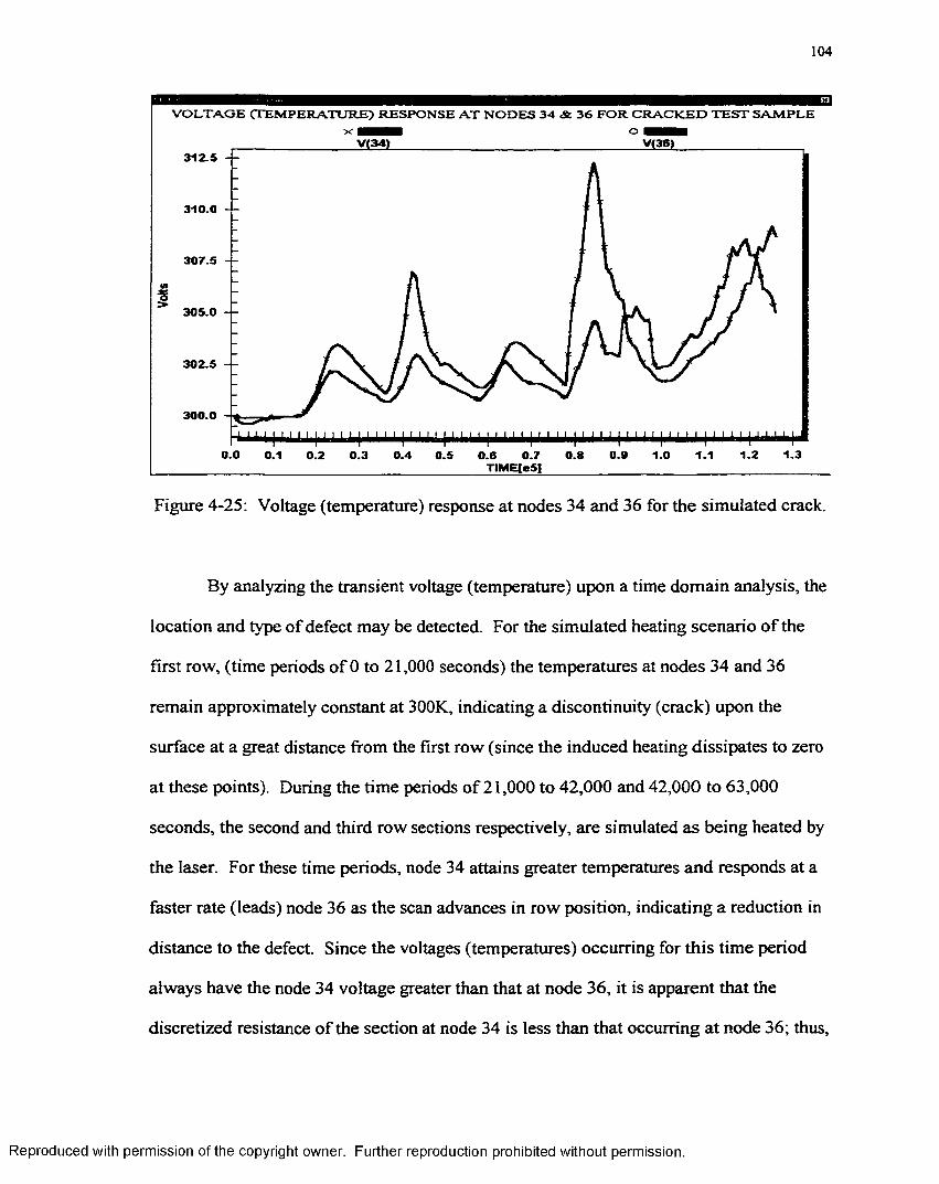
104
VOLTAGE (TEMPERATURE) RESPONSE AT NODES 34 & 36 FOR CRACKED TEST SAMPLEx o
________________V(34)________________________________________ V(36)____________________312.5 -P '
310.0
307.5
305.0
302.5
300.0
0.0 1.2 1.30.1 0.3 0.4 0.5 0.9 1.0 1.10.2 0.80.6
Figure 4-25: Voltage (temperature) response at nodes 34 and 36 for the simulated crack.
By analyzing the transient voltage (temperature) upon a time domain analysis, the
location and type of defect may be detected. For the simulated heating scenario o f the
first row, (time periods of 0 to 2 1,000 seconds) the temperatures at nodes 34 and 36
remain approximately constant at 300K, indicating a discontinuity (crack) upon the
surface at a great distance from the first row (since the induced heating dissipates to zero
at these points). During the time periods of 2 1,000 to 42,000 and 42,000 to 63,000
seconds, the second and third row sections respectively, are simulated as being heated by
the laser. For these time periods, node 34 attains greater temperatures and responds at a
faster rate (leads) node 36 as the scan advances in row position, indicating a reduction in
distance to the defect. Since the voltages (temperatures) occurring for this time period
always have the node 34 voltage greater than that at node 36, it is apparent that the
discretized resistance of the section at node 34 is less than that occurring at node 36; thus,
Reproduced with permission of the copyright owner. Further reproduction prohibited without permission.
105
it may be concluded that node 34 represents the edge and node 36 the center of the crack
defect. As the scan procedure travels to the fourth row, node 36 advances to the leading
position due to the close proximity of this node to the simulated laser position. This
condition exists for the next 3,000 seconds (time period between 63,000 to 66,000
seconds). For the next 12,000 seconds (time periods between 66,000 to 78,000 seconds)
it is assumed that the simulated laser beam is focused within the void o f the crack defect
and contributes no thermal energy to the surface; thus, both nodes begin to cool. This
task is accomplished by not activating the current sources at nodes 26-30 & 35-38 for the
required scan cycle. Node 34 once again assumes the leading position due to the
activation of the node 34 current source to simulate the heated comer o f the next four
scanned sections (time periods o f 78,000 to 90,000 seconds). For the time period
between 90,000 to 120,000 seconds, node 36 assumes the lead of node 34 due to the
proximity (and associated lower resistance) o f the heated section to the referenced node.
Finally during the simulated heating of the last two sections (time periods of 120,000 to
126,000 seconds), node 34 returns to the leading position as the articulated laser more
closely approaches the associated node. The voltage (temperature) transients are now in
correct response for a second scan. This same procedure may be repeated at node 39 to
identify the other edge o f the crack defect.
4.4.5 THE DIFFERENTIAL THERMAL ANALYZER (DTA) SIMULATOR
A material may be tested for surface defects by comparing the thermal transient
results against those for a known, pure sample. From the standpoint o f a simulation, this
can be carried out by obtaining numerical results from two 2D electrical equivalent
Reproduced with permission of the copyright owner. Further reproduction prohibited without permission.
106
circuits simultaneously. In the model, the reference sample would have no defects, and
the test sample would need to have the same dimensions and bulk material characteristics
as the reference standard. In the simulation (or an actual test, if implemented), the
position and movement o f the external laser would move on the reference standard in
unison with that o f the test sample. Each point (as a function o f time) of the test sample
would then be compared with the corresponding point (and time) of the reference
standard to determine if the test sample possessed surface defects. Thus, in a sense, a
SPICE modeled difference amplifier would result.
For concreteness, such a difference amplifier simulation with a pure and an
impure sample was carried out. The fifty six-node circuit o f figure 4-21 was used. The
output voltage o f interest was set equal to the voltage difference between the
corresponding nodes o f the two samples. For example, the difference output voltage for
node 1 may be expressed as:
V node I difference V node 1 of sample " V node I o f reference standard- ( 4 - 9 )
The difference outputs for nodes I through 56 were obtained from nodes 401
through 456, respectively. Under ideal conditions, a perfect test sample compared with a
reference standard should have voltages (temperatures) o f equal magnitude per instant o f
time. Thus, in our simulations, the differential voltage between the two samples was
zero. A mismatch between difference voltages at any instant is indicative of a defect in
the sample. The error signal at node 44 for the previously discussed surface crack
example is presented in figure 4-26.
Reproduced with permission of the copyright owner. Further reproduction prohibited without permission.
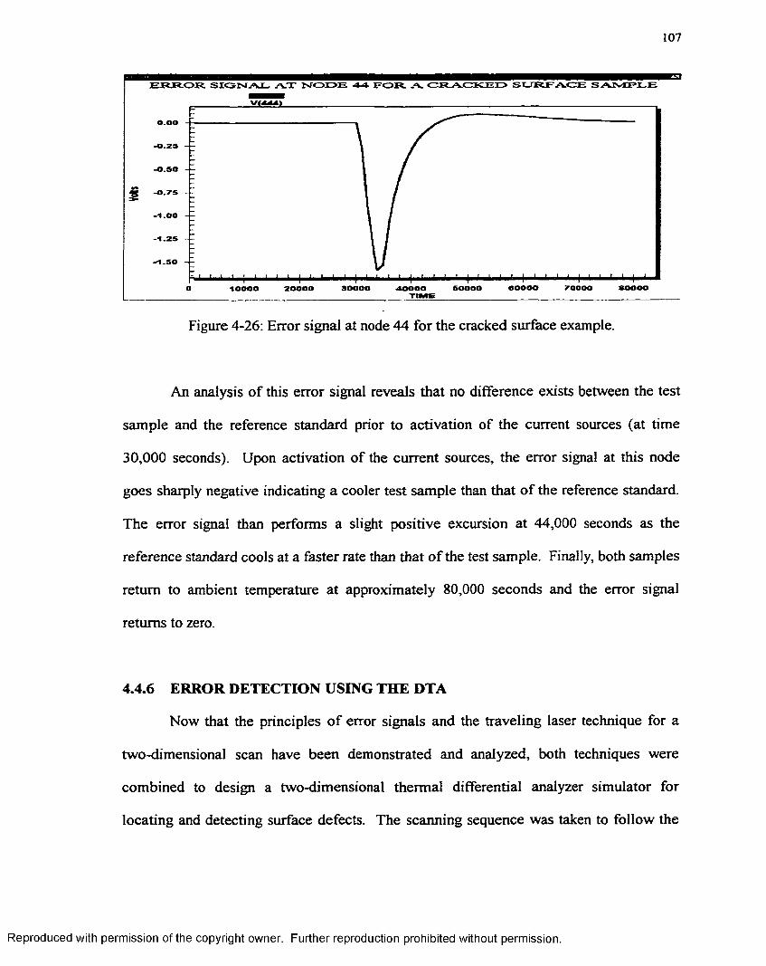
107
0.00
- 0.25
eoooo 2000030000 soooo10000 20000
Figure 4-26: Error signal at node 44 for the cracked surface example.
An analysis of this error signal reveals that no difference exists between the test
sample and the reference standard prior to activation of the current sources (at time
30,000 seconds). Upon activation of the current sources, the error signal at this node
goes sharply negative indicating a cooler test sample than that of the reference standard.
The error signal than performs a slight positive excursion at 44,000 seconds as the
reference standard cools at a faster rate than that o f the test sample. Finally, both samples
return to ambient temperature at approximately 80,000 seconds and the error signal
returns to zero.
4.4.6 ERROR DETECTION USING THE DTA
Now that the principles o f error signals and the traveling laser technique for a
two-dimensional scan have been demonstrated and analyzed, both techniques were
combined to design a two-dimensional thermal differential analyzer simulator for
locating and detecting surface defects. The scanning sequence was taken to follow the
Reproduced with permission of the copyright owner. Further reproduction prohibited without permission.
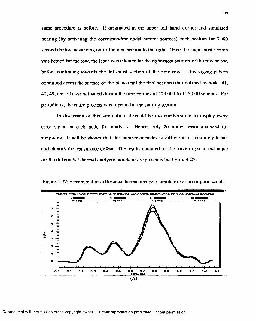
108
same procedure as before. It originated in the upper left hand com er and simulated
heating (by activating the corresponding nodal current sources) each section for 3,000
seconds before advancing on to the next section to the right. Once the right-most section
was heated for the row, the laser was taken to hit the right-most section o f the row below,
before continuing towards the left-most section of the new row. This zigzag pattern
continued across the surface o f the plane until the final section (that defined by nodes 41,
42,49, and 50) was activated during the time periods o f 123,000 to 126,000 seconds. For
periodicity, the entire process was repeated at the starting section.
In discussing o f this simulation, it would be too cumbersome to display every
error signal at each node for analysis. Hence, only 20 nodes were analyzed for
simplicity. It will be shown that this number of nodes is sufficient to accurately locate
and identify the test surface defect. The results obtained for the traveling scan technique
for the differential thermal analyzer simulator are presented as figure 4-27.
Figure 4-27: Error signal of difference thermal analyzer simulator for an impure sample.
EKROR SICe-JAl. OK DOPPERENTIAL THERMAL ANALYZER SIMU1 ATOR FOB. AN IMPURE SAMPLE
x ■ ■ ■ o □ ■■■■■_________V(411)_____________ VI412>______________________V(413)_______________________V(414)
' 1 1 | 1 1 1 1 | ' ' ' 1 | 1 1 1 ' | 1 1 1 1 [ 1 1 1 1 | 1 1 1 ' | 1 1 1 1 | 1 1 1 1 | ' 1 1 ' | 1 1 ' 1 | ' 1 1 1 | 1 ' 1 1 | 0.0 0.1 0.2 0.3 0.4 0.5 0.5 0.7 0.8 0.8 1.0 1.1 1.2 1.3__________________________________________________________TIMEteS] _________
(A)
Reproduced with permission of the copyright owner. Further reproduction prohibited without permission.
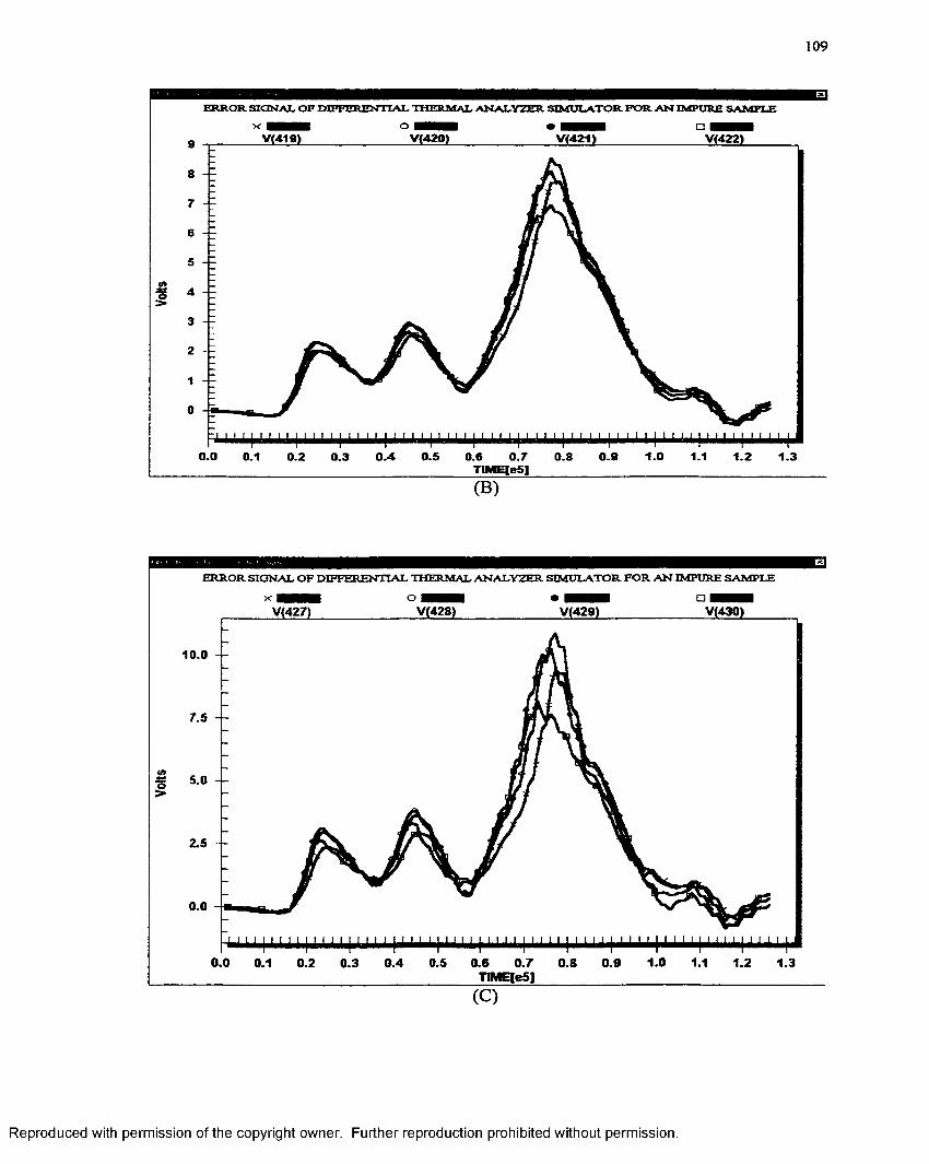
109
ERROR SIGNAL OF DIFFERENTIAL THERMAL ANALYZER SIMULATOR FOR AN IMPURE SAMPLE
x ■■■■ o • ■■■■ aV(420)V(419)9
8
7
6
5
4
3
2
1
0
0.5 1.00.0 0.1 0.4 0.6 0.7 0.9 1.10.2 0.8 1.2 1.30.3TIMHIeSj
(B)
ERROR SIGNAL OF DIFFERENTIAL THERMAL ANALYZER SIMULATOR FOR AN IMPURE SAMPLE
V(427) V(428) V(429) V(430)
(C)
Reproduced with permission of the copyright owner. Further reproduction prohibited without permission.
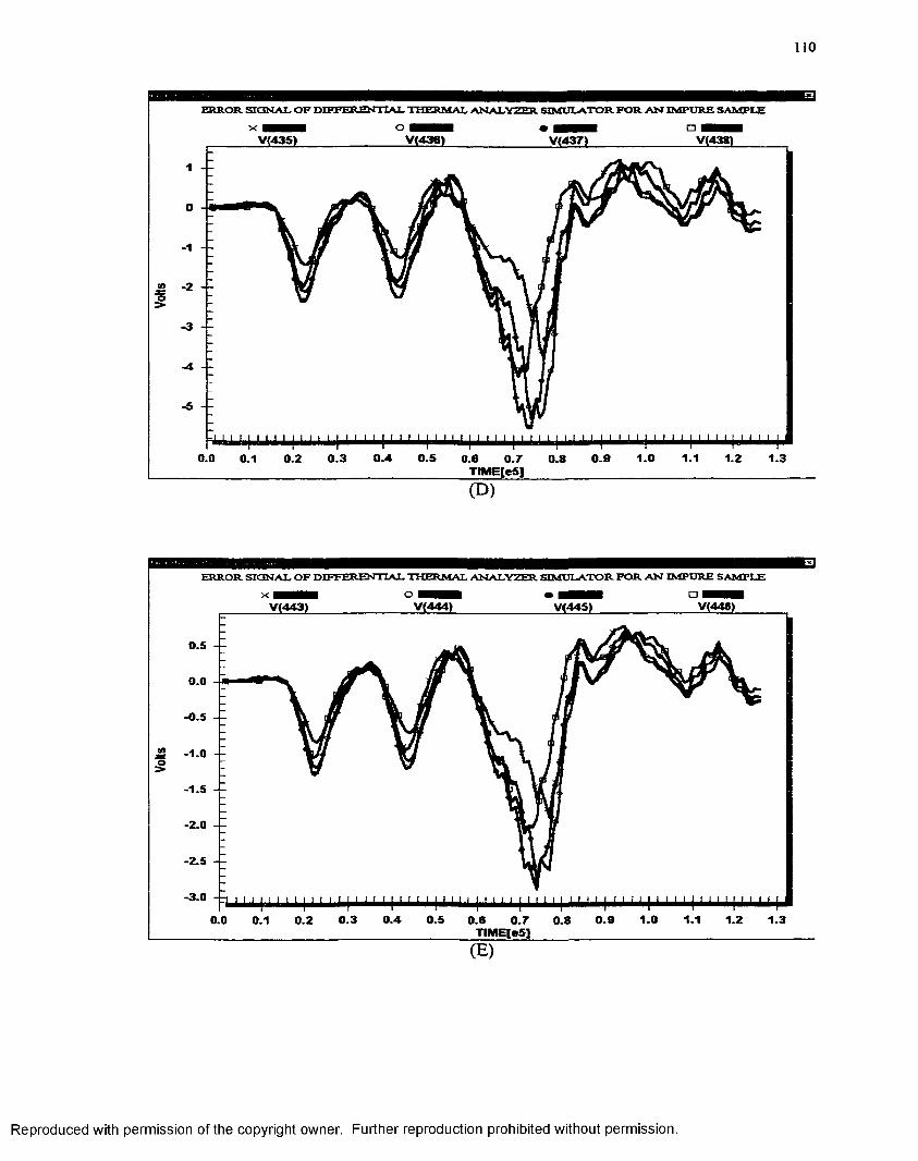
110
ERROR SIGNAL OF DIFFERENTIAL THERMAL ANALYZER SIMULATOR FOR AN IMPURE SAMPLE
x o HBBB • MBBB a
ino>
0.4 0.5 1.0 1.10.0 0.3 0.9 1.2 1.30.1 0.2 0.6 0.7 0.8TIMEIeS]
(D)
ERROR SIGNAL OF DIFFERENTIAL THERMAL ANALYZER SIMULATOR FOR AN IMPURE SAMPLE
x o ^BHB • BBBBB □ BHBBV(443) V<445>
0.5
0.0
•0.5
■1.0
•1.5
■2.0
•2.5
■3.0
0.3 0.4 0.5 1.0 1.10.0 0.9 1.2 1.30.2 0.6 0.7 0.80.1TIMEIeS]
( E )
Reproduced with permission of the copyright owner. Further reproduction prohibited without permission.
I l l
Upon comparing the results o f figure 4-26, it becomes evident that the error o f
greatest magnitude occurs between 60,000 to 105,000 seconds. This time period
corresponds to the simulated heating o f the sections defined by nodes 22-39 which reveal
the location of the defect. Further, the analysis shows that this error is positive in
magnitude for nodes less than 430, and negative in value for nodes greater than 435. This
response matches the behavior observed earlier for a surface crack. Measurement points
(nodes) existing on the same side o f the heating source heat faster and thus obtain a
positive error voltage. Temperatures (voltages) on the surface opposite o f the crack and
heating source experience a delay in transit time (and thus a negative error) around the
crack defect, as well as temperature dissipation during its travel. The temperature
dissipation may be observed by noticing that the magnitude o f error in figures 4-26 (A)-
(C) is greater than that occurring in figure 4-26 (D)-(E). In a practical situation, these
results can be used as crude indicators o f potential defect sites. The rough locations
indicated can subsequently serve as the guide to examine the area more closely by
focusing the laser more narrowly on the physical sample.
4.5 COMMENTS AND DISCUSSION OF RESULTS
A detailed analysis of the single and multiple focused heat pulses provided the
framework for ensuring the validity o f the traveling laser heat source. Simulations o f this
traveling focused heat source technique was applied to ideal one-, two-, and three-
dimensional samples and verified from a thermal viewpoint to ensure an appropriate and
valid behavior existed between the models.
Reproduced with permission of the copyright owner. Further reproduction prohibited without permission.
112
Surface cracks existing upon a two-dimensional sample present a large opposition
to heat flows in the thermal model. Placing a large value resistor at the location o f the
crack easily simulated this scenario. The resistor offered such a large opposition to
electrical current flow (representing conduction heat transfer) that the current had to
travel around the defect creating a delay in the response function and a reduction in the
peak temperature. These changes experienced the greatest delay on the locations directly
opposite the simulated cracked region. These behavior patterns were shown to
qualitatively correspond very well with the expected behavioral trends for both pure and
cracked surface samples. By analyzing the transient voltages (temperatures) upon a time
domain analysis, the location and type o f defect were accurately detected without
reference to a pure test sample.
The differential thermal analyzer (DTA) simulator operated two identical two-
dimensional electrical circuits simultaneously to model heating o f a test structure and a
reference sample, concurrently. An analysis between the magnitude o f the error voltages
and the time that they occurred verified proper electro-thermal relationships for the
differential thermal analyzer simulator and generated the error voltages indicative o f a
physical crack. These results, in themselves, would be sufficient to isolate the location o f
defects in materials.
Reproduced with permission of the copyright owner. Further reproduction prohibited without permission.
113
CHAPTER V
CONCLUSIONS
5.1 OVERVIEW
The heat transport mechanisms and thermal conduction models were all
effectively simulated on the basis o f electrical equivalents. Specifically, only DC
sources, resistors, and capacitors were shown to be sufficient to model the thermal system
completely. Voltage magnitudes in the electrical model corresponded exactly with the
temperatures o f the thermal system representing a valid relationship and equivalence
between the two transport models.
The one-dimensional model compared the transient and steady state response of
both systems to ensure an accurate representation. Here, verification was proven by
comparing the behavior o f the electrical model to that of the thermal model as a function
o f time. Validation of the model was implemented by comparing the voltage and
temperature magnitudes at various times. It has been shown that the accuracy (and
hence, the validity) of the electrical model increased with a reduction in sub-section size.
Two- and three-dimensional models were constructed through simple geometric
combinations o f one-dimensional circuits. The transient and steady state behavior of
these models were analyzed from both an electrical and thermal viewpoint to verify a
correct representation.
Material defects were introduced as large sub-section resistances at the location of
the discrepancy to simulate surface cracks upon the physical sample. The results for the
simulated scanning heat source upon the electrical model corresponded identically with
Reproduced with permission of the copyright owner. Further reproduction prohibited without permission.
114
the expected behavior o f both a pure and a cracked physical sample, verifying sound
simulation procedures for the model.
A differential thermal analyzer simulator was also developed for possible
application to non-intrusive diagnostics. It was applied to a test sample containing a
defect and a reference standard simultaneously. The aim was to evaluate the magnitude
and time delays (if any) for a difference voltage generated at each node as a function o f
time. By observing the temperature differences between the sample and the reference
standard, it was shown that material defects could be correctly located.
5.2 SUMMARY
This thesis research focused on heat and thermal conduction and their role in the
electrical engineering field. The self-heating o f electronic devices and thermal
management issues are o f prime importance in integrated circuit technology.
Temperature increases produced by the internal heat generation affect several parameters
o f electronic devices that collectively alter their overall response characteristics. These
internal temperature increases need to be taken into account for all device optimization
and design procedures.
Computer simulations provide a method to study the response and behavior o f
real world systems through numerical evaluations based on software that is designed to
mimic the system’s operational behavior or characteristics. The simulations employed in
this thesis analyzed thermal transport and heat flow, both under transient and steady state
conditions for a physical sample.
Reproduced with permission of the copyright owner. Further reproduction prohibited without permission.
115
A model allows the analyst to experiment with a representation o f the system and
produce safe and cost effective results. An electrical analogue model was constructed
and analyzed with the SPICE circuit simulator to represent the thermal system. This
equivalent model offered the benefits o f improved efficiency and computational speed for
analyzing the thermal system with parameter alterations.
The five general techniques for analyzing thermal modeling self-heating problems
include the following: Computer Aided Finite Difference Techniques, Computer Based
Finite Element Techniques, The Transmission Line Matrix Method, Thermal Analysis
Using The SPICE Circuit Simulator, and Analytical Techniques and Fourier Series
Solutions.
The Computer Aided Finite Difference Technique assumes that heat flow may be
adequately represented by a non-linear diffusion equation in accordance with Fick’s law.
Although this technique is simple in concept, it is neither a very fast nor accurate method.
As compared to the finite-element method, a larger number of nodes are required for
comparable accuracy. This increase in the matrix size for accuracy then increases the
computational burden. Also, since the final solution is not explicitly expressed in terms
o f an equation, the technique does not provide physical insight and is not very intuitive.
There is a more serious problem with this technique for simulations o f power pulses o f
high magnitude and short durations. Using a smaller time step in the equation may
minimize this problem, but it also significantly increases the computation time.
Computer Based Finite Element Techniques are based upon variational
approximations o f the heat equation. This technique may be applied if rigorous solutions
to complicated geometric structures are desired. The primary difficulty with the FE
Reproduced with permission of the copyright owner. Further reproduction prohibited without permission.
116
method is that it requires a great deal o f expertise and experience to decompose the
geometry into finite elements and set up trial solutions.
The Transmission Line Matrix (TLM) method analyzes a discretized segment of a
semiconductor material as a differential element of a transmission-line circuit. In this
procedure, the heat flow problem is transformed into an equivalent problem o f evaluating
the time dependent propagation of voltage waveforms across the nodes o f a distributed
transmission line network.
The advantage of the TLM method is that it provides an exact time-domain
solution for the network by considering the propagation o f delta pulses from the various
source nodes. The disadvantage of this method is that it is not very well suited for steady
state thermal analysis.
The equivalence between the thermal system o f equations and the variables of
circuit theory, immediately suggests the use o f circuit simulators for the solution of the
thermal problem. This technique compares a differential element of volume within a
semiconductor material denoting a unit cell for the thermal problem to an equivalent
electrical building block. This equivalent electrical network could be solved for a given
set o f current (representing thermal) excitations, using the commercially available SPICE
simulator yielding all node voltages (representing temperatures) as a function o f time.
This approach can easily be generalized to include the temperature dependence of
the thermal conductivity and specific heat by employing voltage controlled resistor and
capacitor elements. The added advantage is that in addition to time-domain analysis, this
technique would easily furnish the frequency response characteristics based on the built-
in capability o f the SPICE simulation tool.
Reproduced with permission of the copyright owner. Further reproduction prohibited without permission.
117
Analytical Techniques and Fourier Series Solutions are the least intensive
computationally and provide closed form expressions for the internal device temperature.
Quantities of interest such as the thermal resistance and peak surface temperatures can
easily be obtained. However, most o f these methods are intended for analysis under
steady state operating conditions.
Electro-thermal modeling began with simulating the heat transfer mechanisms o f
conduction, convection, and radiation. Conduction heat transfer occurs when heat travels
from warmer to cooler objects. The physical model for this transport mechanism
analyzed a bar with constant cross sectional area divided into discretized sections. A
constant heat source existed at the left end o f the bar and the right end was held constant
at ambient temperature.
The electrical model for heat conduction represented each section o f the bar as an
electrical resistance and the temperatures as proportional voltage sources. Resistance
values were computed according to the length and material properties of the
corresponding section. The magnitudes of these resistances assured the proper
distribution of the potential difference between Vheat and Vambient at the voltage nodes
(representing the section junctions) validating the model for steady state thermal
conduction.
Convection heat transfer occurs between a solid boundary and fluid in motion
along its surface. The heat in the thermal model traveled from the gas to the left side o f
the cylinder wall (convection heat transfer), through the cylinder wall (conduction heat
transfer), and from the right side o f the cylinder wall to the coolant (convection heat
transfer).
Reproduced with permission of the copyright owner. Further reproduction prohibited without permission.
118
In order to model this heat transfer mechanism electrically, a series resistance
circuit was created. The temperatures o f the gas and coolant were modeled as
proportional DC voltage sources. Series connected resistors modeled the thermal
resistance for the gas layer, cylinder wall, and coolant.
Thermal radiation is energy emitted by matter as a result o f changes in the
electron configuration o f the atoms or molecules. The mathematical model computes
emitted radiation as a result o f surface temperature and magnitudes for absorption,
reflection, and transmission by their respective coefficients.
A series-parallel electrical network simulated this mechanism. The potential
difference across each resistor related directly to the amount of radiation transferred by
that means.
A one-dimensional model was constructed to simulate unidirectional heat flow
along a single axis. This model was constructed using voltage and current sources,
resistors, and capacitors. These component values were derived from physical properties
o f the thermal model. The voltage source was used to represent the ambient temperature
reference. Current sources were used to simulate the heat generated from a laser beam.
Specific heat of the thermal system was modeled electrically as capacitance. Finally,
resistors were used to represent the thermal conductivity o f the physical model.
The initial state, heating transient, steady-state, cooling transient, and final state of
the thermal model was compared behaviorally and quantitatively with the response of the
electrical model to prove verification and validation between the models. This procedure
was conducted for two models to derive a relationship between sub-section size and
Reproduced with permission of the copyright owner. Further reproduction prohibited without permission.
119
accuracy. A comparison of the results revealed that an increase in accuracy occurred
with a reduction in sub-section size.
One-dimensional analysis then continued with temperature dependant features.
An in-depth investigation of how the electrical and thermal models responded with a
temperature dependant thermal conductivity was presented in this section. This feature
was modeled electrically as voltage controlled resistors and increased both the rate o f
heating and cooling o f the sample and also the maximum temperature attained.
Finally, one-dimensional analysis concluded with analyzing the results obtained
from a focused heat source (which heats the sample at a particular point on the sample), a
cyclic heat source, and a traveling focused heat source.
A two-dimensional sample was constructed o f several intersecting one
dimensional models lying parallel to the x- and y- axis, forming a geometric plane. This
plane was divided into nine equivalent square sections. The comers of each section
existed at a voltage node. When a particular section was simulated as being heated
physically with a laser, the corresponding current sources at the comers were activated to
simulate the introduction of heat. The transient behavior of a traveling laser, heating each
section in succession was analyzed and compared to the electrical model to verify the
relationship between the models.
The three-dimensional model was constructed as a combination o f two two-
dimensional models with several intersecting one-dimensional circuits. In this
representation, it was found that the voltage upon the bottom surface of the sample
responded slower and reached a lower magnitude from that o f the top surface. This
Reproduced with permission of the copyright owner. Further reproduction prohibited without permission.
120
action relates to the physical model in that the heat dissipates and is delayed at the bottom
due to transit time incurred through the material.
Non-intrusive thermal diagnostic (NTID) testing is generally conducted by
subjecting the samples under test to pulsed thermal stimuli. This has become possible
with the advent o f pulsed lasers, which are being used to locally heat sections o f the
samples under test. It has been shown that NIDT requires the analysis of transient
heating and cooling curves at various sections o f a sample when it is subjected to external
laser pulses to induce heating. Initially, the transient behavior o f the traveling focused
heat source is discussed and verified for a pure sample in the absence o f any defects.
Next, material defects are introduced to gauge the differences in the thermal transient
signal.
The laser source provided the energy for localized and directed thermal heating.
In general, advantages of the laser based thermal technique included: (i) High speed by
using the fast laser scanning and/or ultra-short laser pulses, (ii) The ability to magnify
cracks and defects by facilitating a reopening o f pores and cracks as the result o f a
thermal expansion process.
A crack upon the surface o f a body is simulated as a high sub-section resistance at
the location o f the defect. The greater resistance offers an increased opposition to current
flow in the electrical circuit simulating a corresponding hindrance to conduction heat
flow in the thermal model. This surface discontinuity causes heat to travel around the
defect creating a delay in response on the side opposite from the heat source. Also, since
the heat takes a non-direct path to the other side (across the crack), greater heat is
dissipated during its travel causing the resulting temperatures to be o f lower magnitudes
Reproduced with permission of the copyright owner. Further reproduction prohibited without permission.
121
than what would occur if the sample had no defect. It has been proven through
simulations that the voltages existing at the nodes upon the surface o f a two-dimensional
electrical circuit corresponds behaviorally and quantitatively with the temperatures o f the
thermal system (at the same reference points) for the simulated crack defect.
By analyzing the results o f the two-dimensional scanning simulation, the location
and type of defect may be detected by analyzing the transient voltage (temperature) at
selected locations upon a time domain analysis. This process may be simplified with the
aid o f a differential thermal analyzer (DTA) simulator.
The differential thermal analyzer simulator was used to probe a sample for surface
defects by comparing the thermal transient results against those from a known, pure
sample. Each point (as a function o f time) of the test sample was compared with the
corresponding point (and time) o f the reference standard to determine if the test sample
possessed surface defects. The output voltage o f interest was set equal to the voltage
difference (termed the error voltage) between the corresponding nodes o f the two
samples. Using this technique, the location and type of defect was discovered by
observing the location and time at which the greatest error voltage signal occurred.
5.3 SCOPE FOR FUTURE WORK
This thesis served as an introduction to electro-thermal modeling and differential
thermal analysis simulation. The basic concept o f using an electrical equivalent model to
represent a physical material was presented. The work, however, is far from complete.
Much more study of the material is required to advance and perfect this technique.
Thermal analysis may be conducted in the laboratory to validate the conclusions made in
Reproduced with permission of the copyright owner. Further reproduction prohibited without permission.
122
this research. It would be interesting to also work in reverse, by constructing the SPICE
model using a thermal plot o f the material. Other ideas to explore include heating and
cooling durations for the heat source, variations in dielectric properties, and
discontinuities in thermoelectric potentials. The results o f corrosion resistance, changes
in specific heat, and decomposition effects may also be investigated and simulated.
Further analysis may explore the results o f multiple defects on or within (using
the 3D circuit) the sample as well as quantifying the defect from error voltage and time
delay magnitudes.
Improvements in the electrical model may include more available nodes (so that
sub-section size may be minimized) to improve the accuracy o f the model as well as
varactors (voltage-controlled capacitors) to model temperature (voltage) dependant
specific heat.
It is my hope that this research is continued such that more advanced models are
constructed with ever widening practical applications.
Reproduced with permission of the copyright owner. Further reproduction prohibited without permission.
123
REFERENCES
[1]. G. K. Wachutka, “Rigorous Thermodynamic Treatment of Heat Generation and
Conduction in Semiconductor Device Modeling,” IEEE Trans. Comp. A id ed
D esign, Vol. 9, pp 1141-1149, 1990.
[2], W. Liu and B. Bayraktaroglu, “Theoretical Calculations o f Temperature and
Current Profiles in Multi-Finger Heterojunction Bipolar Transistors,” S o lid St.
Electr., Vol. 36, pp 125-132, 1993.
[3], D. de Cogan, “Propagation Analysis for Thermal Modeling,” IEEE Trans.
Component, P ackaging an d M anufacturing Technol. A , Vol. 21, pp 418-423,
1998; and references therein.
[4], F. Profumo, A. Tenconi, S. Facelli, and B. Passerini, “Instantaneous Junction
Temperature Evaluation o f High-Power Diodes During Current Transients,”
IEEE Trans. P ew er Electr., Vol. 14, pp 292-299, 1999.
[5], M. Fan, A. Christou, and M. Pecht, “Two Dimensional Thermal Modeling of
Power Monolithic Microwave Integrated Circuits,” IEEE Trans. Elec. D ev., Vol.
39, pp 1075-1079, 1992.
[6]. V. Ramamurthy, P. K. Chaturvedi, and D. Kakati, “Temperature Rise in
Microwave p-i-n Diodes: A Computer Aided Analysis,” S olid St. E lectr., Vol.
24, pp 445-453, 1981.
[7], H. F. Cooke, “Thermal Effects and Reliability,” in High P o w er G aAs FET
Am plifiers, John Walker, Ed., Boston: Artech House, 1993, pp 227-261.
[8], R. D. Lindsted and R. J. Surty, “Steady-State Junction Temperatures of
Semiconductor Chips,” IEEE Trans. Elec. Derv., Vol. 19, pp 41-44, 1972.
Reproduced with permission of the copyright owner. Further reproduction prohibited without permission.
[9]-
[10].
[11].
[12].
[13].
[14].
[15].
[16].
124
W. Zhou, S. Sheu, J. J. Liou, and C. I. Huang, “Analysis of Non-Uniform Current
and Temperature Distributions in the Emitter Finger o f AlGaAs/GaAs
Heterojunction Bipolar Transistors,” S olid St. E lectr., Vol. 39, pp 1709-1721,
1996.
P. Donzelli, G. Ghione, and C. U. Nidi, “Thermal Models for Low and High
Power Gas MESFET Devices,” G aA s Applications Symp. Conf. P roc., April
1990, pp 120-127.
R. Anholt, in E lec tr ica l a n d Thermal Characterization ofM ESFETs, HEMTs an d
HBTs, Boston: Artech House, 1995.
F. T. Wenthen, “Computer Aided Thermal Analysis of Power Semiconductor
Devices,” IEEE Trans. E lectr. D ev., Vol. 17, pp 765-770, 1970.
G. Liebmann, “The Solution o f Transient Heat Flow and Heat Transfer Problems
by Relaxation,” Brit. J. A ppl. Phys,, Vol. 6, pp 129-135, 1955.
A. Ammous, S. Ghedira, B. Allard, H. Morel, and D. Renault, “Choosing a
Thermal Model for Electrothermal Simulation of Power Semiconductor Devices,”
IEEE Trans. P ow er E lec tr ., Vol. 14, pp 300-307, 1999.
P. B. Johns, “ A Simple Explicit and Unconditionally Stable Numerical Scheme
for the Solution of the Diffusion Equation,” Int. J. Numer. M ethods Engg., Vol.
11, pp 1307-1328, 1977.
A. M. Lohse, P. B. Johns, and A. Wexler, “Computer Graphics for Transient
Fields,” IEEE Trans, on Education , Vol. E-20, pp 64-68, 1977.
Reproduced with permission of the copyright owner. Further reproduction prohibited without permission.
[17].
[18].
[19].
[20].
[21].
[22].
[23].
[24].
[25]
125
P. B. Johns and R. L. Beurle, “Numerical Solution o f Two-Dimensional
Scattering Problems Using a Transmission-Line Matrix,” Proc. Inst. Elec. Eng.,
Vol. 118, pp 1203-1208, 1971.
S. Akhtarzad and P. B. Johns, “Three-Dimensional Transmission-Line Matrix
Computer Analysis o f Microstrip Resonators,” IEEE Trans. M icrow ave Theory
Tech., Vol. MTT-23, pp 990-997, 1975.
F. J. Auerbach, G. Meiendres, R. Muller, and G. J. E. Scheller, “Simulation o f
Thermal Behavior Flow Sensors by Equivalent Electrical Circuits,” Sensors a n d
A ctuators A, Vol. 41-42, pp 275-278, 1994.
S. Ravi Kiran and G. Karunasiri, “Electro-thermal Modeling of Infrared
Microemitters Using PSPICE,” Sensors a n d A ctu a tors A, Vol. 72, pp 110-114,
1999.
M. Necati Ozisik, in H eat Conduction (Wiley, New York, 1993).
C. Kittel and H. Kroemer, in H eat C onduction (W. H. Freeman, San Francisco,
1980).
F. J. Auerbach, G. Meiendres, R. Muller, and G. J. E. Scheller, “Simulation of
Thermal Behavior Flow Sensors by Equivalent Electrical Circuits,” Sensors an d
A ctuators A, Vol. 41-42, pp 275-278, 1994.
S. Ravi Kiran and G. Karunasiri, “Electro-thermal Modeling o f Infrared
Microemitters Using PSPICE,” Sensors an d A ctu a tors A ,
Vol. 72, pp 110-114, 1999.
J. Callaway, Phys. Rev. 113, 1046 (1959); J. Callaway, Phys. Rev. 122, 787
(1961).
Reproduced with permission of the copyright owner. Further reproduction prohibited without permission.
126
[26] J. Callaway and H. C. von Baeyer, Phys. Rev. 120, 1149 (1960).
[27] C. Herring, Phys. Rev. 95, 954 (1954).
[28] P. G. Klemens, in E ncycloped ia o f Physics, edited by S. Flugge (Springer Verlag,
Berlin, 1956), Vol. 14, p. 198.
[29] W. J. de Haas and T. Biermasz, Physica 5, 619 (1938).
[30] R. Berman, Proc. Roy. Soc. (London) A208, 90 (1951).
[31] P. G. Klemens, in S o lid S ta te Physics, edited by F. Seitz and D. Turnbull
(Academic Press, New York, 1958), Vol. 7, p. 1.
[32] R. Peierls, Ann. Physik 3, 1055(1929).
[33] G. A. Slack and S. Galginaitis, Phys. Rev. 133, A253 (1964); C. J. Glassbrenner
and G. A. Slack, Phys. Rev. 134, A1058 (1964).
[34] W. B. Joyce, “Thermal Resistance of Heat Sinks With Temperature-Dependent
Conductivities,” S o lid S ta te E lectronics, Vol. 18, pp 321-322, 1975.
[35] C. Y. Ho, R. W. Powell, and P. E. Liley, in Thermal C on du ctiv ity o f the Elements:
A Com prehensive R eview , New York: American Chemical Society and American
Institute of Physics, 1975.
[36], J. D. Achenbach, “Measurement Models for Quantitative Ultrasonics,” J. Sound
Vibr., Vol. 159, pp 385-401, 1992.
[37], E. Welsch, “Photothermal Surface Deformation Technique: A Goal for
Nondestructive Evaluation in Thin-film Optics.,” Journal o f M o d em O ptics, Vol.
38, pp 2159-2176, 1991.
Reproduced with permission of the copyright owner. Further reproduction prohibited without permission.
127
[38], J. Z. Pan, “Detecting Small Fatigue Cracks by Acoustic Microscopy,” Fatigue
a n d Fracture o f E ngineering M aterials & Structures, Vol. 16, pp 1329-1337,
1993.
[39], S. Suresh, in Fatigue o f M ateria ls , (Cambridge University Press, Cambridge,
1991.)
[40], H. Xiao and P. Nagy, “Enhanced Ultrasonic Detection o f Fatigue Cracks by
Laser-Induced Crack Closure,” J. Appl. Phys., Vol. 83, pp 7453-7460, 1998.
[41], I. Mostafa, S. Hailu, G. Welsch, D. Hazony, and G. R. Halford, “Detection and
Measurement o f Fatigue Crack in HLSA Steel with a Dedicated Ultrasonic Pulse
Transmission Method,” Intl. Journ. O f Fracture, Vol. 85, pp 99-109, 1997.
[42], R. P. Gangloff, R. S. Piascik, D. L. Dicus, and J. C. Newman, Jr., “Fatigue Crack
Propagation in Aerospace Aluminum Alloys,” J. Aircraft, Vol. 31, pp 720-726,
1994.
[43], For example, Q. Shan and R. J. Dewhurst, “Surface-breaking Fatigue Crack
Detection Using Laser Ultrasound,” Appl. Phys. Lett., Vol. 62, pp 2649-2651,
1993.
[44]. J. Krautkramer and H. Krautkramer, in U ltrasonic Testing o f M aterials, (Springer,
Berlin, 1990).
[45], C. B. Scruby and L. E. Drain, in Laser U ltrasonic: Techniques a n d Applications,
(Hilger, Bristol, 1990), pp. 335-350.
[46], J. A. Cooper, R. J. Dewhurst, and S. B. Palmer, “Characterization of Surface
Breaking Defects in Metals With the Use o f Laser Generated Ultrasound,” Philos.
Trans. Roy. Soc., Vol. A 320, pp. 319-328, 1986.
Reproduced with permission of the copyright owner. Further reproduction prohibited without permission.
[47].
[48],
[49],
[50],
[51].
[52].
[53].
[54],
128
R. J. Dewhurst, A. D. W. McKie, and S. B. Palmer, “Further Evidence of Two-
Component Surface Acoustic Wave Reflections from Surface Breaking Slots,”
Appl. Phys. Lett., Vol. 49, pp. 1694-1695, 1986.
D. A. Hutchins, F. Nadeau, and P. Cielo, “A Pulsed Photoacoustic Investigation
o f Ultrasonic Mode Conversion,” Can. J. Phys., Vol. 64, pp. 1334-1340, 1986.
J. A. Ogilvy and J. A. Temple, “Diffraction o f Elastic Waves by Cracks:
Application to Time-of-Flight Inspection,” Ultrasonics, Vol. 21, pp. 259-269,
1983.
F. A. Ravencroft, K. Newton, and C. B. Scruby, “Diffraction o f Ultrasound by
Cracks: Comparison of Experiment with Theory,” U ltrasonics, Vol. 29, pp. 29-
37, 1991.
M. G. Silk, in R esearch Techniques in N on-D estructive Testing, edited by R. S.
Sharp (Academic, N. York, 1977), Vol. 4.
M. N. Bassim, M. Dudar, R. F. Rifaat, and R. Roller, “Application of Acoustic
Emission for Nondestructive Evaluation o f Utility Inductive Reactors,” IEEE
Transactions on P ow er D elivery, Vol. 8, pp. 281-287, 1993.
H. Nayeb-Hashemi, P. Kisnomo, and N. Saniei, “Nondestructive Evaluation of
Fiberglass-Reinforced Plastic Subjected to Localized Heat Damage Using
Acoustic Emission,” Journal o f A cou stic E m ission , Vol. 15, pp. 3342-3348, 1997.
M. Ohtsu, M. Shigeishi, Y. Sakata, “Nondestructive Evaluation o f Defects in
Concrete by Quantitative Acoustic Emission and Ultrasonics,” U ltrasonics, Vol.
36, pp. 187-196, 1998.
Reproduced with permission of the copyright owner. Further reproduction prohibited without permission.
[55].
[56].
[57],
[58],
[59].
[60].
[61].
129
T. Chady, M. Enokizono, and R. Sikora, “Crack Detection and Recognition Using
an Eddy-Current Differential Probe,” IEEE Tram. On Magnetics, Vol. 35, pp.
1849-1852, 1999.
T. Takagi, M. Uesaka, and K. Miya, in Electromagnetic Nondestructive
Evaluation, edited by T. Takagi (IOS Press, N. York, 1997.), pp. 9-14.
R. Albanese, G. Rubinacci, and F. Villone, “An Integral Computational Model for
Crack Simulation and Detection via Eddy-Currents,” Journ. Comput. Physics,
Vol. 152, pp. 736-755, 1999.
W. J. Baxter, “Imaging Short Fatigue Cracks with the Gel Electrode,” Journal of
Testing and Evaluation, Vol. 18, pp. 430-435, 1990.
R. L. Thomas, L. D. Favro, and P. K. Kuo, “Thermal Wave Imaging o f the
Temperature Distributions Around Propagating Cracks in Polymers,” Journal de
Physique IV, Vol. 4, pp. C4:595-601, 1994.
R. L. Thomas, L. D. Favro, and P. K. Kuo, “Thermal Wave Imaging of
Propagating Cracks in Polymers,” Review of Progress in Quantitative
Nondestructive Evaluation, Vol. 13, pp. 1641-1656, 1994.
P. K. Sharp, D. E. Rowlands, and G. Clark, in Technical Report DSTO-TR-0366,
(Defense Science and Technology, Melbourne, 1996).
Reproduced with permission of the copyright owner. Further reproduction prohibited without permission.
130
CURRICULUM VITA for
Michael Stelzer
DEGREES:Master o f Science (Electrical Engineering),
Old Dominion University, Norfolk, Virginia, August 2001
Bachelor o f Science (Electrical Engineering Technology),DeVry Institute o f Technology, Columbus, Ohio, October 1990
SCIENTIFIC AND PROFESSIONAL SOCIETIES MEMBERSHIP:
Electronics Technician Association
HONORS AND AWARDS:
General Radiotelephone Operator’s License with Radar Endorsement, 1999 Senior Certified Electronic Technician, Electronics Technician Association, 1998 Naval Nuclear Power Training Course, U.S. Navy, 1993 Honors Society, DeVry Institute of Technology, 1990 Who’s Who Among American High School Students,
Celina Senior High School, 1985 and 1986
Reproduced with permission of the copyright owner. Further reproduction prohibited without permission.


