Embed Size (px)
Citation preview
3442 IEEE TRANSACTIONS ON ELECTRON DEVICES, VOL. 60, NO. 10, OCTOBER 2013
SPAD Image Sensor With Analog Counting Pixelfor Time-Resolved Fluorescence Detection
Lucio Pancheri, Member, IEEE, Nicola Massari, Member, IEEE, and David Stoppa, Senior Member, IEEE
Abstract— This paper presents a 32 × 32 pixel image sensorfor time-gated fluorescence lifetime detection based on single-photon avalanche diodes. The sensor, fabricated in a high-voltage 0.35-µm CMOS technology, uses an analog countingapproach to minimize the area occupation of pixel electronicswhile maintaining a nanosecond timing resolution and shot-noise-limited operation. The all nMOS pixel is formed by 12transistors and features 25-µm pitch and 20.8% fill factor. Thechip includes a phase-locked loop circuit for gating window gen-eration, working at a maximum repetition frequency of 40 MHz,while the sensor can be gated at frequency up to 80 MHzusing an external delay generator. Optical characterization with apicosecond-pulsed laser showed a minimum gating window widthof 1.1 ns. Example images acquired in both continuous and time-gated mode are presented, together with a lifetime image obtainedwith the sensor mounted on a fluorescence microscope.
Index Terms— Analog counter, CMOS image sensor,fluorescence lifetime imaging (FLIM), single-photon avalanchediode (SPAD), time gating.
I. INTRODUCTION
SEVERAL scientific imaging applications require sensorspossessing both high sensitivity and nanosecond or sub-
nanosecond timing resolution. Among others, it is worthmentioning fluorescence lifetime imaging (FLIM), Ramanspectroscopy, time-resolved near-infrared spectroscopy, andpositron-emission tomography.
A good selection of commercial sensors for high-sensitivityimaging is available. Cooled CCDs, electron-multiplyingCCDs, and scientific CMOS sensors feature very high quan-tum efficiencies and extremely low noise levels [1], [2]. Fornonimaging or scanning applications, photomultiplier tubes,microchannel plates, and single-photon avalanche diodes(SPAD) [3] can provide a single detector channel or smallarrays with high sensitivity and picosecond timing resolutions.The combination of the two properties in an imaging detectoris almost unique. The only commercially available image sen-sors combining single-photon sensitivity and subnanosecondtiming resolution are time-gated intensified CCDs (I-CCDs),which can reach shot-noise-limited performance and can beoperated with gate widths as low as 200 ps [4].
Manuscript received March 15, 2013; revised June 10, 2013; acceptedJuly 29, 2013. Date of publication August 22, 2013; date of current versionSeptember 18, 2013. This work was supported by the Project NAoMI, financedby the Provincia Autonoma of Trento. The review of this paper was arrangedby Editor J. R. Tower.
L. Pancheri is with the Department of Industrial Engineering, University ofTrento, Trento 38123, Italy (e-mail: [email protected]).
N. Massari and D. Stoppa are with Fondazione Bruno Kessler, Trento 38023,Italy (e-mail: [email protected]; [email protected]).
Color versions of one or more of the figures in this paper are availableonline at http://ieeexplore.ieee.org.
Digital Object Identifier 10.1109/TED.2013.2276752
Most of the time-resolved CMOS sensors developed inthe last decade have been specifically designed for time-of-flight (ToF) optical ranging [5]. Although the applicability ofsensors developed for ToF to fluorescence imaging has beendemonstrated in principle, they require further improvement insensitivity and timing resolution to be competitive in scientificimaging applications [6]. The use of customized pinned-photodiode technologies could combine the low noise of state-of-the-art active pixels with the nanosecond timing resolutionneeded in FLIM application [7], [8].
Among the possible CMOS compatible detectors, SPADsoffer the most natural solution for time-resolved fluorescenceimaging. They feature both an excellent timing resolution, inthe order of 100 ps and single-photon sensitivity. In spite oftheir high potential, there are, however, still several issues tobe solved for their effective applicability in imaging arrays.
The first problem is technological. CMOS processes areusually not tailored for optimized SPAD performance. Thehigh doping levels typically used in CMOS well implantationscause a high tunneling contribution to dark count rate (DCR),while the thick surface passivation layers reduce the achievablephoton detection probability. However, several recent attemptsto optimize the process have led to devices with very goodcharacteristics fabricated in CMOS image sensor technologies[9]–[11].
The second problem is related to achievable pixel fill factorthat is limited by both the SPAD guard ring and by the in-pixelprocessing circuits. To overcome this problem, the guard ringsize can be minimized [12] and the fill factor can be recoveredusing optical concentrators [13]. However, SPAD arrays withconcentrators having good yield and uniformity have not yetbeen demonstrated.
The third problem is architectural since each detected pho-ton generates an event that needs to be processed, even in low-resolution arrays a huge bandwidth is necessary to transmitthe data, unless the signal is processed and stored at the pixellevel. In this case, however, additional pixel storage circuitsneed to be integrated, with further reduction of pixel fill factor.If the image sensors based on SPADs presented so far areanalyzed, it can be noticed that in 2-D arrays the fill factorachieved is very small, in the order of a few percent, due tothe aforementioned constraints [14]–[17]. In linear sensors, thesituation is better, although the area occupied by electronics istypically much larger than the one occupied by the detectors[12], [18], [19].
In this paper, we demonstrate an approach that could over-come the previously described limitations in 2-D arrays. Usingan in-pixel counting circuit working in the analog domain,the pixel electronics can be kept compact while maintaining
0018-9383 © 2013 IEEE
PANCHERI et al.: SPAD IMAGE SENSOR WITH ANALOG COUNTING PIXEL 3443
shot-noise-limited operation and nanosecond timing capabil-ities. The analog counting approach was already proposedfor X-ray counting in hybrid and monolithic pixel detectors[20], [21] and for SPAD pixels in [22], but a high fill-factor2-D SPAD array exploiting this concept is demonstrated herefor the first time. The sensor described in this paper wasfirst presented in [23]. More details about the architectureimplementation and an extended characterization are reportedhere, to show the full potential of the proposed approach andunderline the possible future improvements.
This paper is organized as follows. Section II describestime-gated detection principle, pixel design, and chip archi-tecture. Section III presents the sensor experimental charac-terization, calibration, and operation in FLIM applications.
II. SENSOR DESIGN
A. Time-Gated Detection
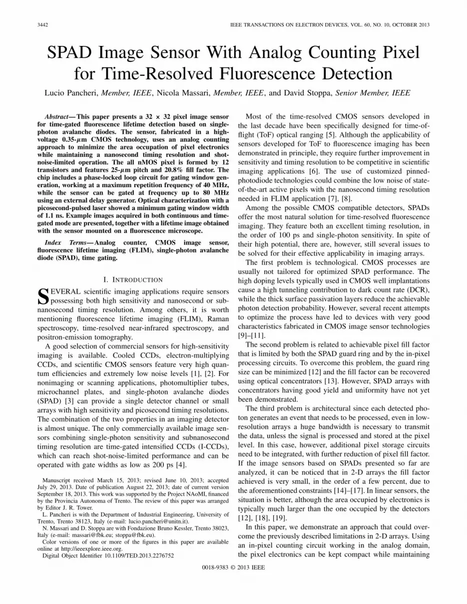
The operation principle of time-gated fluorescence detectionis schematically shown in Fig. 1. A picosecond-pulsed lasersource is used to excite the fluorescence in the sample underanalysis. The fluorescence signal is delivered to a detectorthrough an optical system that includes an objective andfilters for excitation light removal. A series of observationwindows is opened, starting after the decay of the laser pulse.The optimal width of the gating windows �t is related tothe fluorescence decay time, which is in the nanosecond orsubnanosecond range for most of the fluorescent markersused in biology and biophysics [24]. To obtain informationabout the decay time, fluorescence signal needs to be acquiredwithin two or more measurement windows. With the simplestconfiguration, using only two windows, monoexponential flu-orescence lifetime τ can be estimated [25] from
τ = �T ln
(C2
C1
)(1)
where �T is the time offset between the two observationwindows and C1 and C2 are the number of signal countsinside the two windows. In the presence of a multiexponentialdecay, as often observed in practical applications, more thantwo gating windows can be used to estimate the different decaytime constants.
If compared with time-correlated single-photon counting(TCSPC) technique, time gating is particularly suitable forarray implementation. For TCSPC, a time-to-digital/time-to-amplitude converter should be implemented at the pixel level,recording the arrival time of each detected photon. In this way,the pixel signal has to be acquired after every photon detectionevent, thus requiring high frame-rate readout [14]. For highresolution arrays, this approach presents problems of signalbandwidth and power consumption. In a time-gated pixel, onthe contrary, the number of detected photons can be storedinside an in-pixel counter, thus avoiding the need to read outthe array at high speed.
In time-gated SPAD sensors, either the SPAD or the countercan be gated, depending on the target application. In the firstcase, the SPAD is switched rapidly on and off, thus enablingphoton detection only inside the gating window [26]–[29].
Δt2Δt1 Δt3 ΔtN
Laser excitation pulse
Fluorescenceemission
Time
Ligh
tint
ensi
ty
Pulsed laser
Fluorescentsample
Time-gateddetector
Objective
Opticalfilter cube
Fig. 1. Operation principle of time-gated detection.
A
SPADMonostable AND gate
Analogcounter
Source follower +select transistor
Quenchingtransistor
B C D
Col
umn
bus
WIN
Gating circuit
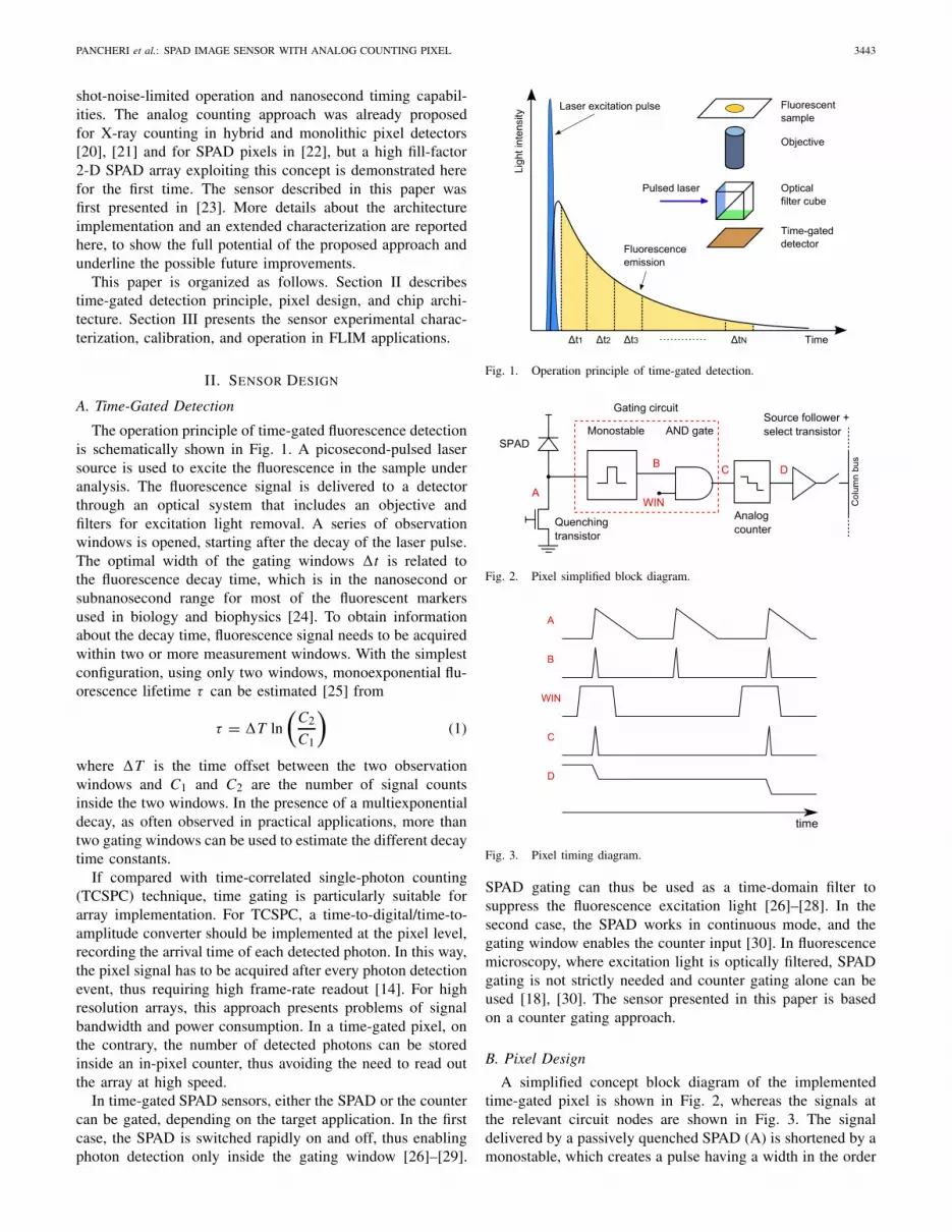
Fig. 2. Pixel simplified block diagram.
A
B
C
D
WIN
time
Fig. 3. Pixel timing diagram.
SPAD gating can thus be used as a time-domain filter tosuppress the fluorescence excitation light [26]–[28]. In thesecond case, the SPAD works in continuous mode, and thegating window enables the counter input [30]. In fluorescencemicroscopy, where excitation light is optically filtered, SPADgating is not strictly needed and counter gating alone can beused [18], [30]. The sensor presented in this paper is basedon a counter gating approach.
B. Pixel Design
A simplified concept block diagram of the implementedtime-gated pixel is shown in Fig. 2, whereas the signals atthe relevant circuit nodes are shown in Fig. 3. The signaldelivered by a passively quenched SPAD (A) is shortened by amonostable, which creates a pulse having a width in the order
3444 IEEE TRANSACTIONS ON ELECTRON DEVICES, VOL. 60, NO. 10, OCTOBER 2013
(b)
WIN
TUONI
WIN
IN OUT(a)
Fig. 4. Gating circuit. (a) Extended implementation. (b) Compact implemen-tation.
M1
M2
M3
M4
M5
M6
M7
M8
M9
M10M11
M12
Vbq
VbAC
WIN
DIS VbPU VbPU RESVbSPAD
Col
umn
bus
SEL
SPAD front-end Gating circuit Analog counter
CINT
C1
Fig. 5. Pixel schematic diagram.
of a few 100 s of picoseconds. The shortened pulse is thenconvoluted with a gating window (WIN) through an AND gate.The pulse shortening is needed to maintain a subnanosecondtiming resolution that would be lost without this operation.Another possibility to obtain ultrafast gating is the use ofan edge-triggered flip-flop [18], [27], which would, however,require a larger area and has therefore been discarded in thisimplementation.
The pulses at node (C) are passed to an analog countercircuit, delivering an output voltage (D) proportional to thenumber of input counts. Using an analog approach, the count-ing function can be implemented with a very compact circuit,at the expense of an additional A/D conversion after pixelreadout. If the voltage step �V corresponding to a photondetection is much larger than the pixel noise, however, it is stillpossible to discriminate the single photons in the analog outputsignal and a shot-noise-limited operation can be maintained.As in a conventional active pixel, a source follower and aselect transistor complete the pixel schematic.
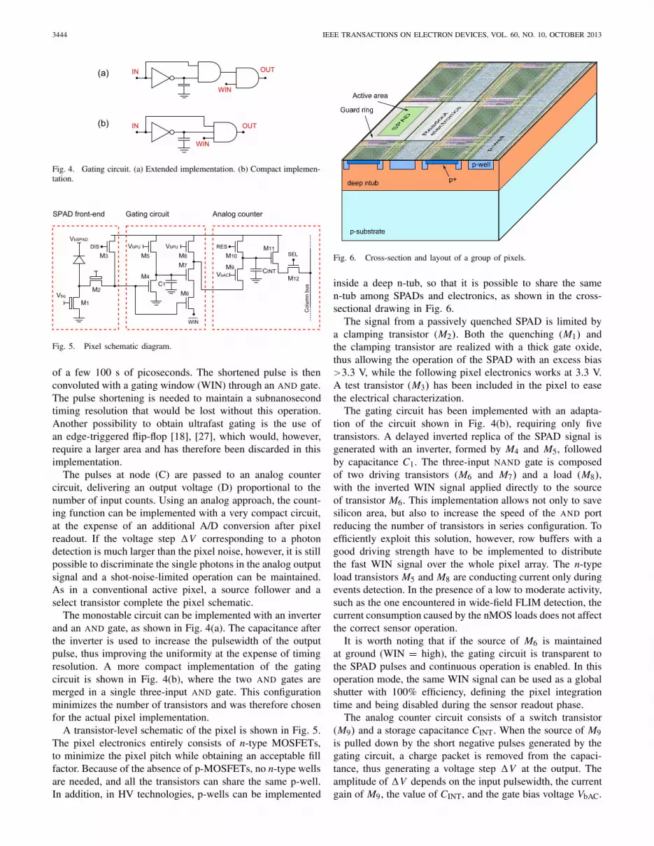
The monostable circuit can be implemented with an inverterand an AND gate, as shown in Fig. 4(a). The capacitance afterthe inverter is used to increase the pulsewidth of the outputpulse, thus improving the uniformity at the expense of timingresolution. A more compact implementation of the gatingcircuit is shown in Fig. 4(b), where the two AND gates aremerged in a single three-input AND gate. This configurationminimizes the number of transistors and was therefore chosenfor the actual pixel implementation.
A transistor-level schematic of the pixel is shown in Fig. 5.The pixel electronics entirely consists of n-type MOSFETs,to minimize the pixel pitch while obtaining an acceptable fillfactor. Because of the absence of p-MOSFETs, no n-type wellsare needed, and all the transistors can share the same p-well.In addition, in HV technologies, p-wells can be implemented
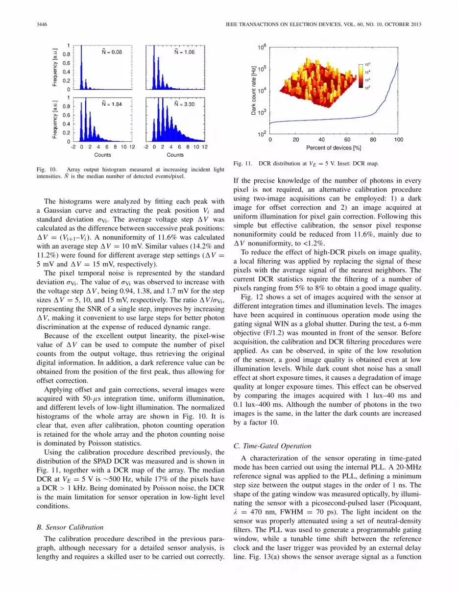
Fig. 6. Cross-section and layout of a group of pixels.
inside a deep n-tub, so that it is possible to share the samen-tub among SPADs and electronics, as shown in the cross-sectional drawing in Fig. 6.
The signal from a passively quenched SPAD is limited bya clamping transistor (M2). Both the quenching (M1) andthe clamping transistor are realized with a thick gate oxide,thus allowing the operation of the SPAD with an excess bias>3.3 V, while the following pixel electronics works at 3.3 V.A test transistor (M3) has been included in the pixel to easethe electrical characterization.
The gating circuit has been implemented with an adapta-tion of the circuit shown in Fig. 4(b), requiring only fivetransistors. A delayed inverted replica of the SPAD signal isgenerated with an inverter, formed by M4 and M5, followedby capacitance C1. The three-input NAND gate is composedof two driving transistors (M6 and M7) and a load (M8),with the inverted WIN signal applied directly to the sourceof transistor M6. This implementation allows not only to savesilicon area, but also to increase the speed of the AND portreducing the number of transistors in series configuration. Toefficiently exploit this solution, however, row buffers with agood driving strength have to be implemented to distributethe fast WIN signal over the whole pixel array. The n-typeload transistors M5 and M8 are conducting current only duringevents detection. In the presence of a low to moderate activity,such as the one encountered in wide-field FLIM detection, thecurrent consumption caused by the nMOS loads does not affectthe correct sensor operation.
It is worth noting that if the source of M6 is maintainedat ground (WIN = high), the gating circuit is transparent tothe SPAD pulses and continuous operation is enabled. In thisoperation mode, the same WIN signal can be used as a globalshutter with 100% efficiency, defining the pixel integrationtime and being disabled during the sensor readout phase.
The analog counter circuit consists of a switch transistor(M9) and a storage capacitance CINT. When the source of M9is pulled down by the short negative pulses generated by thegating circuit, a charge packet is removed from the capaci-tance, thus generating a voltage step �V at the output. Theamplitude of �V depends on the input pulsewidth, the currentgain of M9, the value of CINT, and the gate bias voltage VbAC.

PANCHERI et al.: SPAD IMAGE SENSOR WITH ANALOG COUNTING PIXEL 3445
Fig. 7. Chip block diagram.
While the first three parameters are fixed during the designphase, the fourth one provides an electrical programmabilityof the voltage step.
The pixel is completed with a reset transistor (M10), asource follower (M11), and a select switch (M12). Since theinterface with the column bus is the same as in a standardactive pixel, the same peripheral circuitry architectures usedin conventional CMOS image sensors can be exploited.
The design was implemented in a commercial 0.35-μmhigh-voltage CMOS technology. The pictorial representationof a group of pixels is shown in Fig. 6. The SPAD has thesame structure reported in [26], with a p+/deep n-tub activearea and a p-well guard ring. In this implementation, the SPADactive area is rectangular and the corners of the guard ringare cut at 45°, to avoid excessive electric-field intensification.The nMOS readout electronics are placed within p-well stripesimplemented inside the deep n-tub. Using this arrangement,the area occupied by the guard ring could be minimized, anda pixel with 25-μm pitch and 20.8% fill factor was obtained.
C. Chip Architecture
A block diagram of the chip is shown in Fig. 7. The sensorincludes a 32 × 32 pixel array, row and column decoders,and a series of row buffers to provide the gating signal (WIN)to the pixel. A simple analog buffer is used for the readout.Although not optimized for high speed and low noise, thisconfiguration was chosen because it provides the maximumflexibility for the pixel experimental characterization.
A digital phase-locked loop (PLL) was also implementedon-chip for gating signal (WIN) generation. The core of thePLL is a 24-stage ring oscillator, designed to operate at a maxi-mum frequency of 40 MHz. A multiplexer is used to select twosignals from the ring oscillator to define the rising and fallingedge of the gating window WIN. For maximum flexibility,start and stop signals can also be provided externally.
III. EXPERIMENTAL RESULTS
A. Pixel Characterization
This section reports the experimental results from anelectro-optical characterization of the sensor. The measure-
1.82
1.83
1.84
1.85
1.86
1.87
1.88
1.89
1.9
0 0.5 1 1.5 2 2.5 3
Out
put v
olta
ge [V
]
Time [ms]
Fig. 8. Oscilloscope traces of pixel output in continuous operation mode.
0100200300400500600
-10 0 10 20 30 40 50 60 70 80
Cou
nts
Voltage [mV]
∆V = 10mV
0200
400600
8001000
Cou
nts
∆V = 5mV
Fig. 9. Pixel output histograms for two different voltage step settings.
ments were performed with the SPADs biased at an excessvoltage VE = 5 V, either in the dark or in low-light levelconditions.
The unity gain output buffer allows the direct observation ofthe pixel output voltage during signal integration. Two oscil-loscope traces of the pixel voltage in continuous acquisitionoperation (WIN = high) are shown in Fig. 8. A staircasecharacteristic can be observed, indicating the possibility toclearly discriminate the output photons.
Pixel output nonlinearity was estimated after averaging alarge number of oscilloscope traces acquired in the presenceof a moderate pixel illumination. Using this procedure, thevariability due to the random event arrival time is reduced toa negligible level, allowing the estimation of systematic pixelnonlinearity. The averaged voltage trace could be fitted with astraight line with an error lower than 0.5% across 1.5 V range.
The output signal was digitized with an off-chip 12-bitADC, having a resolution of ∼1 mV. For each pixel, a largenumber of acquisitions (typically in the order of 104) wereperformed to calculate the output voltage histogram. As anexample, two histograms of the same pixel acquired withdifferent VbAC settings are shown in Fig. 9. The shape of thehistograms is determined by the convolution of the Poissondistribution of detection events inside the integration windowwith the electronic noise of the readout chain.
3446 IEEE TRANSACTIONS ON ELECTRON DEVICES, VOL. 60, NO. 10, OCTOBER 2013
Fig. 10. Array output histogram measured at increasing incident lightintensities. Ñ is the median number of detected events/pixel.
The histograms were analyzed by fitting each peak witha Gaussian curve and extracting the peak position Vi andstandard deviation σVi. The average voltage step �V wascalculated as the difference between successive peak positions:�V = (Vi+1–Vi ). A nonuniformity of 11.6% was calculatedwith an average step �V = 10 mV. Similar values (14.2% and11.2%) were found for different average step settings (�V =5 mV and �V = 15 mV, respectively).
The pixel temporal noise is represented by the standarddeviation σVi. The value of σVi was observed to increase withthe voltage step �V , being 0.94, 1.38, and 1.7 mV for the stepsizes �V = 5, 10, and 15 mV, respectively. The ratio �V /σVi,representing the SNR of a single step, improves by increasing�V, making it convenient to use large steps for better photondiscrimination at the expense of reduced dynamic range.
Because of the excellent output linearity, the pixel-wisevalue of �V can be used to compute the number of pixelcounts from the output voltage, thus retrieving the originaldigital information. In addition, a dark reference value can beobtained from the position of the first peak, thus allowing foroffset correction.
Applying offset and gain corrections, several images wereacquired with 50-μs integration time, uniform illumination,and different levels of low-light illumination. The normalizedhistograms of the whole array are shown in Fig. 10. It isclear that, even after calibration, photon counting operationis retained for the whole array and the photon counting noiseis dominated by Poisson statistics.
Using the calibration procedure described previously, thedistribution of the SPAD DCR was measured and is shown inFig. 11, together with a DCR map of the array. The medianDCR at VE = 5 V is ∼500 Hz, while 17% of the pixels havea DCR > 1 kHz. Being dominated by Poisson noise, the DCRis the main limitation for sensor operation in low-light levelconditions.
B. Sensor Calibration
The calibration procedure described in the previous para-graph, although necessary for a detailed sensor analysis, islengthy and requires a skilled user to be carried out correctly.
Fig. 11. DCR distribution at VE = 5 V. Inset: DCR map.
If the precise knowledge of the number of photons in everypixel is not required, an alternative calibration procedureusing two-image acquisitions can be employed: 1) a darkimage for offset correction and 2) an image acquired atuniform illumination for pixel gain correction. Following thissimple but effective calibration, the sensor pixel responsenonuniformity could be reduced from 11.6%, mainly due to�V nonuniformity, to <1.2%.
To reduce the effect of high-DCR pixels on image quality,a local filtering was applied by replacing the signal of thesepixels with the average signal of the nearest neighbors. Thecurrent DCR statistics require the filtering of a number ofpixels ranging from 5% to 8% to obtain a good image quality.
Fig. 12 shows a set of images acquired with the sensor atdifferent integration times and illumination levels. The imageshave been acquired in continuous operation mode using thegating signal WIN as a global shutter. During the test, a 6-mmobjective (F/1.2) was mounted in front of the sensor. Beforeacquisition, the calibration and DCR filtering procedures wereapplied. As can be observed, in spite of the low resolutionof the sensor, a good image quality is obtained even at lowillumination levels. While dark count shot noise has a smalleffect at short exposure times, it causes a degradation of imagequality at longer exposure times. This effect can be observedby comparing the images acquired with 1 lux–40 ms and0.1 lux–400 ms. Although the number of photons in the twoimages is the same, in the latter the dark counts are increasedby a factor 10.
C. Time-Gated Operation
A characterization of the sensor operating in time-gatedmode has been carried out using the internal PLL. A 20-MHzreference signal was applied to the PLL, defining a minimumstep size between the output stages in the order of 1 ns. Theshape of the gating window was measured optically, by illumi-nating the sensor with a picosecond-pulsed laser (Picoquant,λ = 470 nm, FWHM = 70 ps). The light incident on thesensor was properly attenuated using a set of neutral-densityfilters. The PLL was used to generate a programmable gatingwindow, while a tunable time shift between the referenceclock and the laser trigger was provided by an external delayline. Fig. 13(a) shows the sensor average signal as a function
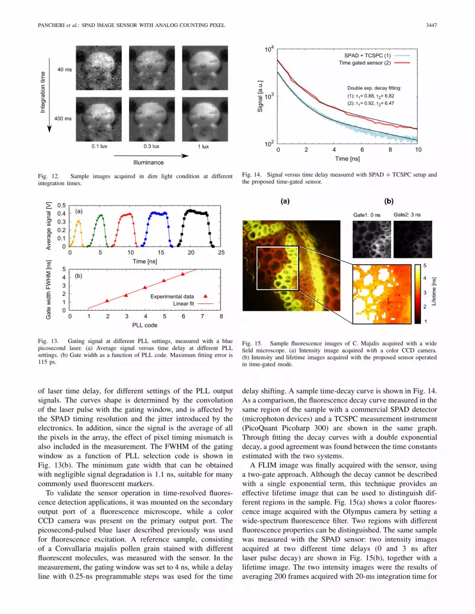
PANCHERI et al.: SPAD IMAGE SENSOR WITH ANALOG COUNTING PIXEL 3447
Fig. 12. Sample images acquired in dim light condition at differentintegration times.
012345
0 1 2 3 4 5 6 7 8Gat
e w
idth
FW
HM
[ns]
PLL code
(b)
Experimental dataLinear fit
00.10.20.30.40.5
0 5 10 15 20 25
Ave
rage
sig
nal [
V]
Time [ns]
(a)
Fig. 13. Gating signal at different PLL settings, measured with a bluepicosecond laser. (a) Average signal versus time delay at different PLLsettings. (b) Gate width as a function of PLL code. Maximum fitting error is115 ps.
of laser time delay, for different settings of the PLL outputsignals. The curves shape is determined by the convolutionof the laser pulse with the gating window, and is affected bythe SPAD timing resolution and the jitter introduced by theelectronics. In addition, since the signal is the average of allthe pixels in the array, the effect of pixel timing mismatch isalso included in the measurement. The FWHM of the gatingwindow as a function of PLL selection code is shown inFig. 13(b). The minimum gate width that can be obtainedwith negligible signal degradation is 1.1 ns, suitable for manycommonly used fluorescent markers.
To validate the sensor operation in time-resolved fluores-cence detection applications, it was mounted on the secondaryoutput port of a fluorescence microscope, while a colorCCD camera was present on the primary output port. Thepicosecond-pulsed blue laser described previously was usedfor fluorescence excitation. A reference sample, consistingof a Convallaria majalis pollen grain stained with differentfluorescent molecules, was measured with the sensor. In themeasurement, the gating window was set to 4 ns, while a delayline with 0.25-ns programmable steps was used for the time
102
103
104
0 2 4 6 8 10
Sig
nal [
a.u.
]
Time [ns]
Double exp. decay fitting:(1): τ1= 0.88, τ2= 6.82(2): τ1= 0.92, τ2= 6.47
SPAD + TCSPC (1)Time gated sensor (2)
Fig. 14. Signal versus time delay measured with SPAD + TCSPC setup andthe proposed time-gated sensor.
Fig. 15. Sample fluorescence images of C. Majalis acquired with a widefield microscope. (a) Intensity image acquired with a color CCD camera.(b) Intensity and lifetime images acquired with the proposed sensor operatedin time-gated mode.
delay shifting. A sample time-decay curve is shown in Fig. 14.As a comparison, the fluorescence decay curve measured in thesame region of the sample with a commercial SPAD detector(microphoton devices) and a TCSPC measurement instrument(PicoQuant Picoharp 300) are shown in the same graph.Through fitting the decay curves with a double exponentialdecay, a good agreement was found between the time constantsestimated with the two systems.
A FLIM image was finally acquired with the sensor, usinga two-gate approach. Although the decay cannot be describedwith a single exponential term, this technique provides aneffective lifetime image that can be used to distinguish dif-ferent regions in the sample. Fig. 15(a) shows a color fluores-cence image acquired with the Olympus camera by setting awide-spectrum fluorescence filter. Two regions with differentfluorescence properties can be distinguished. The same samplewas measured with the SPAD sensor: two intensity imagesacquired at two different time delays (0 and 3 ns afterlaser pulse decay) are shown in Fig. 15(b), together with alifetime image. The two intensity images were the results ofaveraging 200 frames acquired with 20-ms integration time for
3448 IEEE TRANSACTIONS ON ELECTRON DEVICES, VOL. 60, NO. 10, OCTOBER 2013
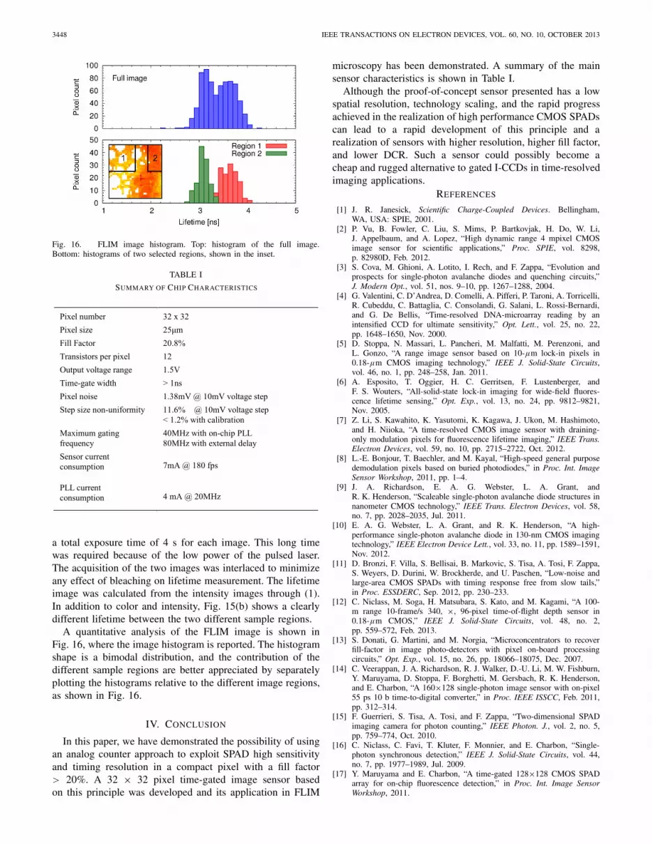
Fig. 16. FLIM image histogram. Top: histogram of the full image.Bottom: histograms of two selected regions, shown in the inset.
TABLE I
SUMMARY OF CHIP CHARACTERISTICS
a total exposure time of 4 s for each image. This long timewas required because of the low power of the pulsed laser.The acquisition of the two images was interlaced to minimizeany effect of bleaching on lifetime measurement. The lifetimeimage was calculated from the intensity images through (1).In addition to color and intensity, Fig. 15(b) shows a clearlydifferent lifetime between the two different sample regions.
A quantitative analysis of the FLIM image is shown inFig. 16, where the image histogram is reported. The histogramshape is a bimodal distribution, and the contribution of thedifferent sample regions are better appreciated by separatelyplotting the histograms relative to the different image regions,as shown in Fig. 16.
IV. CONCLUSION
In this paper, we have demonstrated the possibility of usingan analog counter approach to exploit SPAD high sensitivityand timing resolution in a compact pixel with a fill factor> 20%. A 32 × 32 pixel time-gated image sensor basedon this principle was developed and its application in FLIM
microscopy has been demonstrated. A summary of the mainsensor characteristics is shown in Table I.
Although the proof-of-concept sensor presented has a lowspatial resolution, technology scaling, and the rapid progressachieved in the realization of high performance CMOS SPADscan lead to a rapid development of this principle and arealization of sensors with higher resolution, higher fill factor,and lower DCR. Such a sensor could possibly become acheap and rugged alternative to gated I-CCDs in time-resolvedimaging applications.
REFERENCES
[1] J. R. Janesick, Scientific Charge-Coupled Devices. Bellingham,WA, USA: SPIE, 2001.
[2] P. Vu, B. Fowler, C. Liu, S. Mims, P. Bartkovjak, H. Do, W. Li,J. Appelbaum, and A. Lopez, “High dynamic range 4 mpixel CMOSimage sensor for scientific applications,” Proc. SPIE, vol. 8298,p. 82980D, Feb. 2012.
[3] S. Cova, M. Ghioni, A. Lotito, I. Rech, and F. Zappa, “Evolution andprospects for single-photon avalanche diodes and quenching circuits,”J. Modern Opt., vol. 51, nos. 9–10, pp. 1267–1288, 2004.
[4] G. Valentini, C. D’Andrea, D. Comelli, A. Pifferi, P. Taroni, A. Torricelli,R. Cubeddu, C. Battaglia, C. Consolandi, G. Salani, L. Rossi-Bernardi,and G. De Bellis, “Time-resolved DNA-microarray reading by anintensified CCD for ultimate sensitivity,” Opt. Lett., vol. 25, no. 22,pp. 1648–1650, Nov. 2000.
[5] D. Stoppa, N. Massari, L. Pancheri, M. Malfatti, M. Perenzoni, andL. Gonzo, “A range image sensor based on 10-μm lock-in pixels in0.18-μm CMOS imaging technology,” IEEE J. Solid-State Circuits,vol. 46, no. 1, pp. 248–258, Jan. 2011.
[6] A. Esposito, T. Oggier, H. C. Gerritsen, F. Lustenberger, andF. S. Wouters, “All-solid-state lock-in imaging for wide-field fluores-cence lifetime sensing,” Opt. Exp., vol. 13, no. 24, pp. 9812–9821,Nov. 2005.
[7] Z. Li, S. Kawahito, K. Yasutomi, K. Kagawa, J. Ukon, M. Hashimoto,and H. Niioka, “A time-resolved CMOS image sensor with draining-only modulation pixels for fluorescence lifetime imaging,” IEEE Trans.Electron Devices, vol. 59, no. 10, pp. 2715–2722, Oct. 2012.
[8] L.-E. Bonjour, T. Baechler, and M. Kayal, “High-speed general purposedemodulation pixels based on buried photodiodes,” in Proc. Int. ImageSensor Workshop, 2011, pp. 1–4.
[9] J. A. Richardson, E. A. G. Webster, L. A. Grant, andR. K. Henderson, “Scaleable single-photon avalanche diode structures innanometer CMOS technology,” IEEE Trans. Electron Devices, vol. 58,no. 7, pp. 2028–2035, Jul. 2011.
[10] E. A. G. Webster, L. A. Grant, and R. K. Henderson, “A high-performance single-photon avalanche diode in 130-nm CMOS imagingtechnology,” IEEE Electron Device Lett., vol. 33, no. 11, pp. 1589–1591,Nov. 2012.
[11] D. Bronzi, F. Villa, S. Bellisai, B. Markovic, S. Tisa, A. Tosi, F. Zappa,S. Weyers, D. Durini, W. Brockherde, and U. Paschen, “Low-noise andlarge-area CMOS SPADs with timing response free from slow tails,”in Proc. ESSDERC, Sep. 2012, pp. 230–233.
[12] C. Niclass, M. Soga, H. Matsubara, S. Kato, and M. Kagami, “A 100-m range 10-frame/s 340, ×, 96-pixel time-of-flight depth sensor in0.18-μm CMOS,” IEEE J. Solid-State Circuits, vol. 48, no. 2,pp. 559–572, Feb. 2013.
[13] S. Donati, G. Martini, and M. Norgia, “Microconcentrators to recoverfill-factor in image photo-detectors with pixel on-board processingcircuits,” Opt. Exp., vol. 15, no. 26, pp. 18066–18075, Dec. 2007.
[14] C. Veerappan, J. A. Richardson, R. J. Walker, D.-U. Li, M. W. Fishburn,Y. Maruyama, D. Stoppa, F. Borghetti, M. Gersbach, R. K. Henderson,and E. Charbon, “A 160×128 single-photon image sensor with on-pixel55 ps 10 b time-to-digital converter,” in Proc. IEEE ISSCC, Feb. 2011,pp. 312–314.
[15] F. Guerrieri, S. Tisa, A. Tosi, and F. Zappa, “Two-dimensional SPADimaging camera for photon counting,” IEEE Photon. J., vol. 2, no. 5,pp. 759–774, Oct. 2010.
[16] C. Niclass, C. Favi, T. Kluter, F. Monnier, and E. Charbon, “Single-photon synchronous detection,” IEEE J. Solid-State Circuits, vol. 44,no. 7, pp. 1977–1989, Jul. 2009.
[17] Y. Maruyama and E. Charbon, “A time-gated 128×128 CMOS SPADarray for on-chip fluorescence detection,” in Proc. Int. Image SensorWorkshop, 2011.

PANCHERI et al.: SPAD IMAGE SENSOR WITH ANALOG COUNTING PIXEL 3449
[18] L. Pancheri and D. Stoppa, “A SPAD-based pixel linear array for high-speed time-gated fluorescence lifetime imaging,” in Proc. ESSCIRC,Sep. 2009, pp. 428–431.
[19] Y. Maruyama, J. Blacksberg, and E. Charbon, “A 1024×8, 0.7 ns time-gated SPAD line sensor for laser Raman spectroscopy and LIBS inspace and Rover based planetary exploration,” in Proc. IEEE ISSCC,Aug. 2013, pp. 110–111.
[20] M. Perenzoni, D. Stoppa, M. Malfatti, and A. Simoni, “A multispectralanalog photon-counting readout circuit for X-ray hybrid pixel detectors,”IEEE Trans. Instrum. Meas., vol. 57, no. 7, pp. 1438–1444, Jul. 2008.
[21] B. Dierickx, B. Dupont, A. Defernez, and N. Ahmed, “Indirect X-rayphoton-counting image sensor with 27T pixel and 15e−rms accuratethreshold,” in Proc. IEEE ISSCC, Feb. 2011, pp. 114–115.
[22] D. Stoppa, F. Borghetti, J. A. Richardson, R. J. Walker, L. Grant,R. K. Henderson, M. Gersbach, and E. Charbon, “A 32×32-pixel arraywith in-pixel photon counting and arrival time measurement in theanalog domain,” in Proc. IEEE ESSCIRC, Sep. 2009, pp. 204–207.
[23] L. Pancheri, N. Massari, F. Borghetti, and D. Stoppa, “A 32×32 SPADpixel array with nanosecond gating and analog readout,” in Proc. Int.Image Sensor Workshop, 2011.
[24] J. R. Lakowicz, Principles of Fluorescence Spectroscopy. New York,NY, USA: Plenum, 1999.
[25] H. C. Gerritsen, M. A. H. Asselbergs, A. V. Agronskaia, andW. G. J. H. M. Van Sark, “Fluorescence lifetime imaging in scanningmicroscopes: Acquisition speed, photon economy and lifetime resolu-tion,” J. Microscopy, vol. 206, no. 3, pp. 218–224, Jun. 2002.
[26] D. Stoppa, D. Mosconi, L. Pancheri, and L. Gonzo, “Single-photonavalanche diode CMOS sensor for time-resolved fluorescence measure-ments,” IEEE Sensors J., vol. 9, no. 9, pp. 1084–1090, Sep. 2009.
[27] B. R. Rae, C. Griffin, K. R. Muir, J. M. Girkin, E. Gu, D. R. Renshaw,E. Charbon, M. D. Dawson, and R. K. Henderson, “A microsystemfor time-resolved fluorescence analysis using CMOS single-photonavalanche diodes and micro-LEDs,” in Proc. IEEE ISSCC, Feb. 2008,pp. 166–603.
[28] A. Dalla Mora, A. Tosi, F. Zappa, S. Cova, D. Contini, A. Pifferi,L. Spinelli, A. Torricelli, and R. Cubeddu, “Fast-gated single-photonavalanche diode for wide dynamic range near infrared spectroscopy,”IEEE J. Sel. Topics Quantum Electron., vol. 16, no. 4, pp. 1023–1030,Jul. 2010.
[29] I. Nissinen, J. Nissinen, A. Lansman, L. Hallman, A. Kilpela,J. Kostamovaara, M. Kogler, M. Aikio, J. Tenhunen, “A sub-ns time-gated CMOS single photon avalanche diode detector for Raman spec-troscopy,” in Proc. ESSDERC, Sep. 2011, pp. 375–378.
[30] D. E. Schwartz, E. Charbon, and K. L. Shepard, “A single-photonavalanche diode array for fluorescence lifetime imaging microscopy,”IEEE J. Solid-State Circuits, vol. 43, no. 11, pp. 2546–2557, Nov. 2008.
Lucio Pancheri (M’11) received the Ph.D. degree ininformation and communication technologies fromthe University of Trento, Trento, Italy, in 2006.
He has been a Researcher with the University ofTrento since 2012.
Nicola Massari (M’08) received the Laurea degreein electronic engineering from the University ofPadova, Padova, Italy, in 1999.
He has been with Fondazione Bruno Kessler asa Researcher with the Smart Optical Sensors andInterfaces Research Unit since 2000.
David Stoppa (M’97–SM’12) received the Ph.D.degree in microelectronics from the University ofTrento, Trento, Italy, in 2002.
He has been head of the Smart Optical Sensorsand Interfaces Research Unit at Fondazione BrunoKessler, since 2010.


