Embed Size (px)
Citation preview
This article appeared in a journal published by Elsevier. The attachedcopy is furnished to the author for internal non-commercial researchand education use, including for instruction at the authors institution
and sharing with colleagues.
Other uses, including reproduction and distribution, or selling orlicensing copies, or posting to personal, institutional or third party
websites are prohibited.
In most cases authors are permitted to post their version of thearticle (e.g. in Word or Tex form) to their personal website orinstitutional repository. Authors requiring further information
regarding Elsevier’s archiving and manuscript policies areencouraged to visit:
http://www.elsevier.com/copyright
Author's personal copy
SiO2 etch rate modification by ion implantation
E. Bellandi ⁎, V. SonciniMicron Italia srl via C. Olivetti 2, 20864 Agrate Brianza (MB), Italy
a b s t r a c ta r t i c l e i n f o
Article history:Received 21 February 2012Received in revised form 21 September 2012Accepted 21 September 2012Available online 5 October 2012
Keywords:Ion implantationEtch rate profileImplantation damageSRIM
The structural damage of silicon dioxide films produced by different ion species has been studied by etch rateprofiling. The etch rate showed a good correlation with the damage estimated by a simulation software. Theetch rate increases almost linearly up to a certain damage level then it saturates to a value which depends onthe implanted ion and on the etching chemistry. This suggests a different kind of damage mechanism inducedby the different implanted ions.
© 2012 Elsevier B.V. All rights reserved.
1. Introduction
It is well known that etch rate of dielectric thin films, such as silicondioxide, increases after ion implantation. A studyof the structural damagecreated in SiO2 films by ion implantation can be found in references [1,2].It is reported that nuclear collision of implanted ion with target ions pro-duces a relevant rearrangement of SiO2 target network: Si and O targetatoms are moved from their original positions to new positions whereoriginal local atomic coordination is not recovered. Asfinal result, damageconsists mainly of Si\O broken bonds and non-bridging oxygen.
A model that can predict the amount of implanted film etched offas a function of implanted specie, dose, energy and etching chemistrywould be of practical interest for many purposes such as the oxiderecession after gate oxide and self aligned silicide pre-cleans.
Etch rate profiling is a very sensitive technique for the damageevaluation, even if it requires a high accuracy and a large number ofexperiments to produce significant data.
In this paper we study the effect of As, In, P and B ion implantation onthe etch rate of a thermally grownsilicondioxidefilm. Twoetching chem-istries have beenused for our experiments: diluted hydrofluoric acid (HF)and diluted buffered oxide etch (BOE, HF:NH4F:H2O). The latter behavesdifferently from the commonly used concentrated BOEs (e.g. 1:100–500HF:NH4F mixtures) used for example for contact cleanings. In fact theetching rate of the water diluted solutions (HF:NH4F:H2O having a lowHF:NH4F ratio and a high amount of water) of weak oxides is enhancedinstead of being reduced, but it offers an improved etch uniformity, alower cost and a low silicon etch.
2. Experimental details
In our experiments, a 5500 Å thick SiO2 layer, thermally grown onp-type b100> Si substrates (1.7–2.5 Ωcm) by a wet oxidation, hasbeen implanted with arsenic, indium, phosphorous and boron at asingle energy and at three different doses (see Table 1).
Etch rate profiles were obtained using 0.3% HF (nominal etchrate~18 Å/min) and diluted BOE (nominal etch rate~45Å/min).
Etch rate profiles were obtained by a sequence of short etchingsteps. An as-grown sample (no ion implantation) has been used asreference in each etching batch and the etching rate was obtainedmeasuring the layer thickness before and after each step on 5 pointsper wafer. Relative etch rate is defined as the ratio of the sampleetch rate and the reference thermal oxide etch rate. This procedurehas been described in reference [3].
All the experiments were performed in a 200 mm Class 1 cleanroom, using common production equipment: a DNS FC 821L was usedto run both chemistries and the oxide thickness was measured by aKLA-Tencor spectroscopic ellipsometer. Implantation of boron, phos-phorus and arsenic was performed by an Axcelis Ultra whilst indiumwas implanted by a Varian E500HP.
The simulations of the implantation damage were performed bySRIM [4].
3. Results and discussion
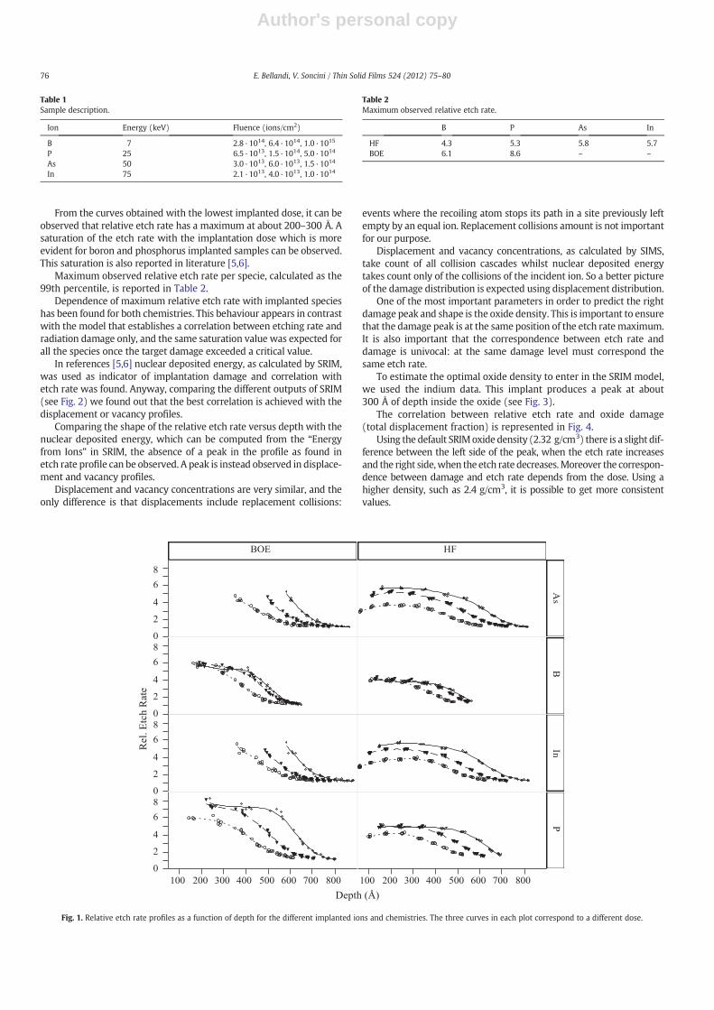
The plot of the relative etch rate as a function of the depth fromthe oxide layer surface is reported in Fig. 1.
All the samples show a significant impact of the ion implantationon the etch rate and the etch rate can be over seven times higherthan the one measured on the reference oxide without implantation.
Thin Solid Films 524 (2012) 75–80
⁎ Corresponding author. Tel.: +39 0396377195.E-mail address: [email protected] (E. Bellandi).
0040-6090/$ – see front matter © 2012 Elsevier B.V. All rights reserved.http://dx.doi.org/10.1016/j.tsf.2012.09.060
Contents lists available at SciVerse ScienceDirect
Thin Solid Films
j ourna l homepage: www.e lsev ie r .com/ locate / ts f
Author's personal copy
From the curves obtained with the lowest implanted dose, it can beobserved that relative etch rate has a maximum at about 200–300 Å. Asaturation of the etch rate with the implantation dose which is moreevident for boron and phosphorus implanted samples can be observed.This saturation is also reported in literature [5,6].
Maximum observed relative etch rate per specie, calculated as the99th percentile, is reported in Table 2.
Dependence of maximum relative etch rate with implanted specieshas been found for both chemistries. This behaviour appears in contrastwith the model that establishes a correlation between etching rate andradiation damage only, and the same saturation value was expected forall the species once the target damage exceeded a critical value.
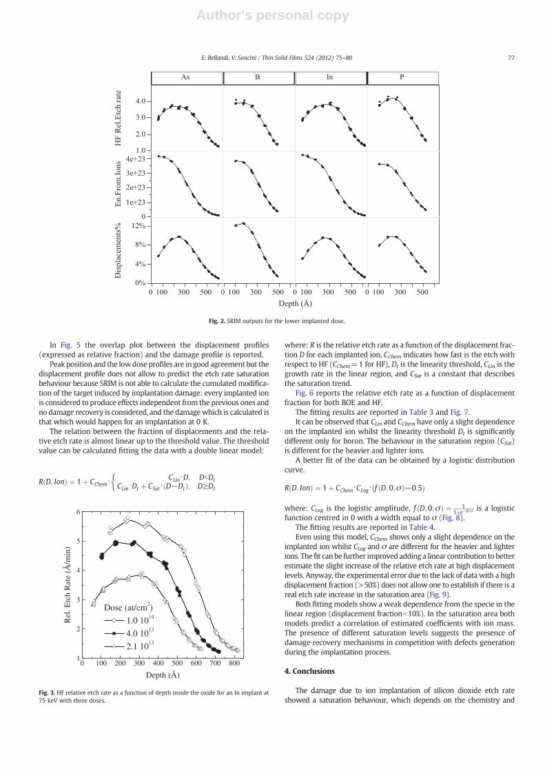
In references [5,6] nuclear deposited energy, as calculated by SRIM,was used as indicator of implantation damage and correlation withetch rate was found. Anyway, comparing the different outputs of SRIM(see Fig. 2) we found out that the best correlation is achieved with thedisplacement or vacancy profiles.
Comparing the shape of the relative etch rate versus depth with thenuclear deposited energy, which can be computed from the “Energyfrom Ions” in SRIM, the absence of a peak in the profile as found inetch rate profile can be observed. A peak is instead observed in displace-ment and vacancy profiles.
Displacement and vacancy concentrations are very similar, and theonly difference is that displacements include replacement collisions:
events where the recoiling atom stops its path in a site previously leftempty by an equal ion. Replacement collisions amount is not importantfor our purpose.
Displacement and vacancy concentrations, as calculated by SIMS,take count of all collision cascades whilst nuclear deposited energytakes count only of the collisions of the incident ion. So a better pictureof the damage distribution is expected using displacement distribution.
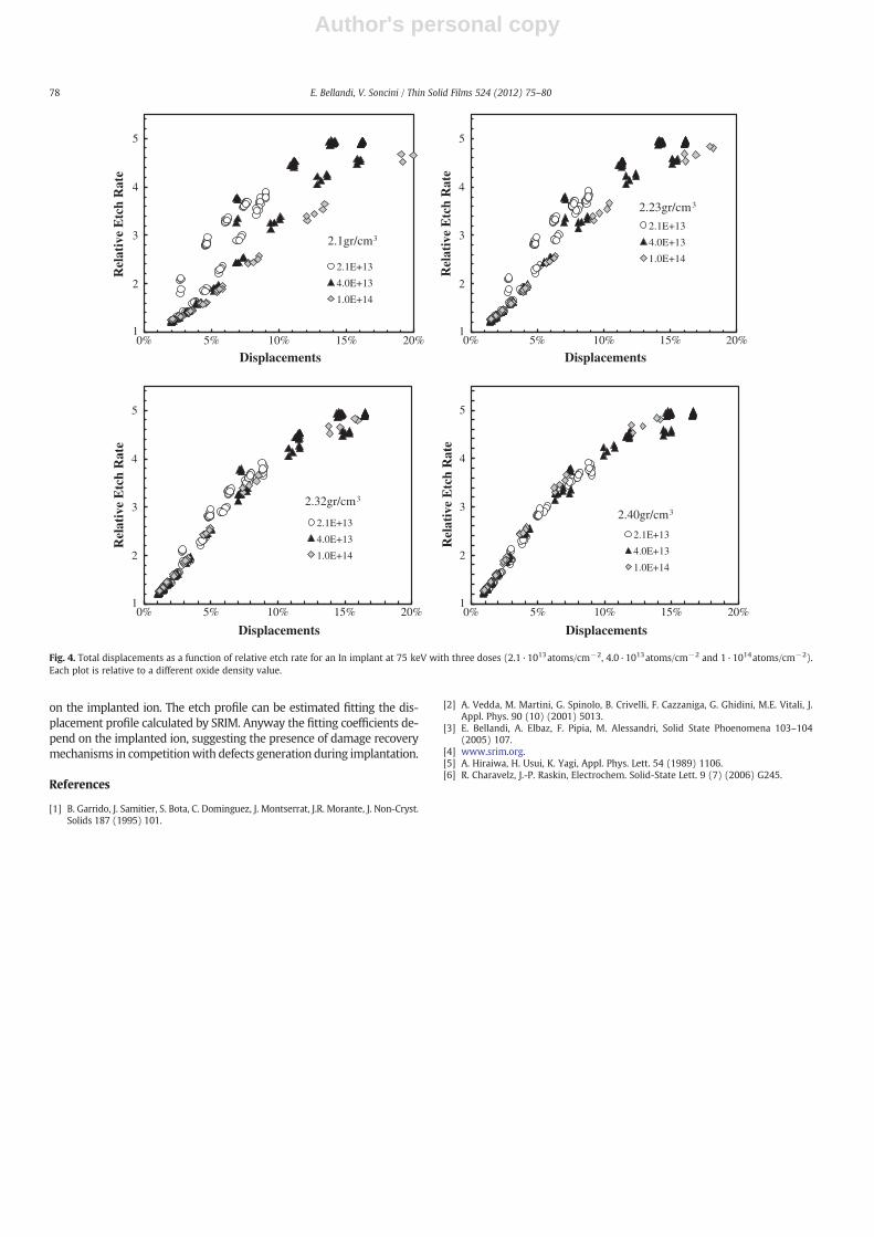
One of the most important parameters in order to predict the rightdamage peak and shape is the oxide density. This is important to ensurethat the damage peak is at the same position of the etch ratemaximum.It is also important that the correspondence between etch rate anddamage is univocal: at the same damage level must correspond thesame etch rate.
To estimate the optimal oxide density to enter in the SRIM model,we used the indium data. This implant produces a peak at about300 Å of depth inside the oxide (see Fig. 3).
The correlation between relative etch rate and oxide damage(total displacement fraction) is represented in Fig. 4.
Using the default SRIMoxide density (2.32 g/cm3) there is a slight dif-ference between the left side of the peak, when the etch rate increasesand the right side,when the etch rate decreases.Moreover the correspon-dence between damage and etch rate depends from the dose. Using ahigher density, such as 2.4 g/cm3, it is possible to get more consistentvalues.
Table 1Sample description.
Ion Energy (keV) Fluence (ions/cm2)
B 7 2.8·1014, 6.4·1014, 1.0·1015
P 25 6.5·1013, 1.5·1014, 5.0·1014
As 50 3.0·1013, 6.0·1013, 1.5·1014
In 75 2.1·1013, 4.0·1013, 1.0·1014
sn
Fig. 1. Relative etch rate profiles as a function of depth for the different implanted ions and chemistries. The three curves in each plot correspond to a different dose.
Table 2Maximum observed relative etch rate.
B P As In
HF 4.3 5.3 5.8 5.7BOE 6.1 8.6 – –
76 E. Bellandi, V. Soncini / Thin Solid Films 524 (2012) 75–80
Author's personal copy
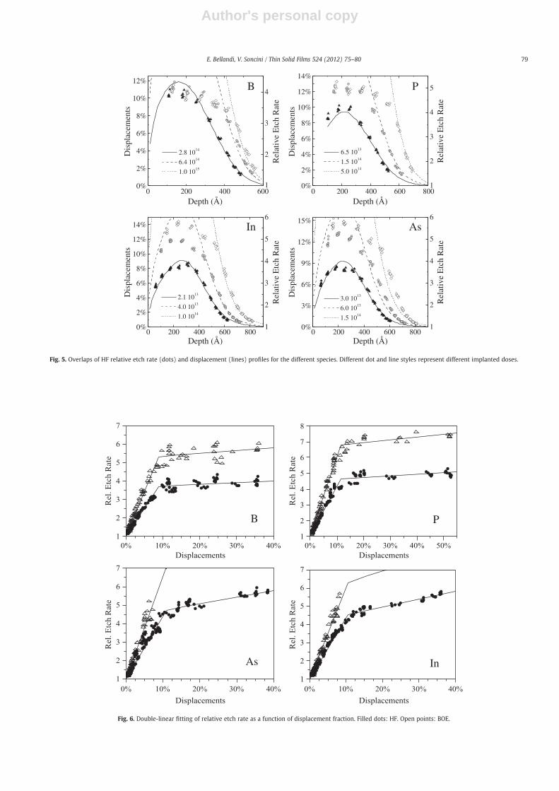
In Fig. 5 the overlap plot between the displacement profiles(expressed as relative fraction) and the damage profile is reported.
Peak position and the lowdose profiles are in good agreement but thedisplacement profile does not allow to predict the etch rate saturationbehaviour because SRIM is not able to calculate the cumulatedmodifica-tion of the target induced by implantation damage: every implanted ionis considered to produce effects independent from the previous ones andno damage recovery is considered, and the damagewhich is calculated isthat which would happen for an implantation at 0 K.
The relation between the fraction of displacements and the rela-tive etch rate is almost linear up to the threshold value. The thresholdvalue can be calculated fitting the data with a double linear model:
R D; Ionð Þ ¼ 1þ CChem⋅CLin⋅D; DbDt
CLin⋅Dt þ CSat⋅ D−Dtð Þ; D≥Dt
�
where: R is the relative etch rate as a function of the displacement frac-tion D for each implanted ion, CChem indicates how fast is the etch withrespect to HF (CChem=1 for HF), Dt is the linearity threshold, CLin is thegrowth rate in the linear region, and CSat is a constant that describesthe saturation trend.
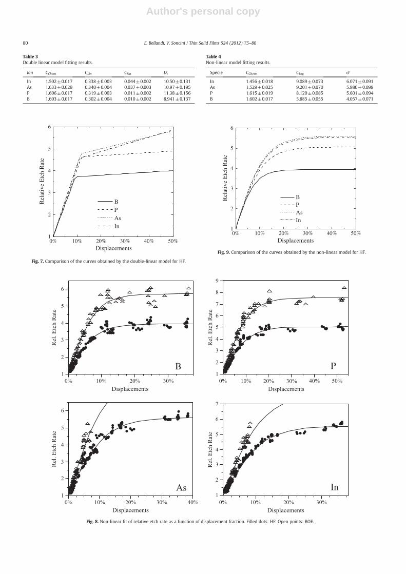
Fig. 6 reports the relative etch rate as a function of displacementfraction for both BOE and HF.
The fitting results are reported in Table 3 and Fig. 7.It can be observed that CLin and CChem have only a slight dependence
on the implanted ion whilst the linearity threshold Dt is significantlydifferent only for boron. The behaviour in the saturation region (CSat)is different for the heavier and lighter ions.
A better fit of the data can be obtained by a logistic distributioncurve.
R D; Ionð Þ ¼ 1þ CChem⋅CLog⋅ f D;0;σð Þ−0:5ð Þ
where: CLog is the logistic amplitude, f D;0;σð Þ ¼ 11þe−D=σ is a logistic
function centred in 0 with a width equal to σ (Fig. 8).The fitting results are reported in Table 4.Even using this model, CChem shows only a slight dependence on the
implanted ion whilst CLog and σ are different for the heavier and lighterions. Thefit canbe further improved adding a linear contribution to betterestimate the slight increase of the relative etch rate at high displacementlevels. Anyway, the experimental error due to the lack of datawith a highdisplacement fraction (>50%) does not allow one to establish if there is areal etch rate increase in the saturation area (Fig. 9).
Both fittingmodels show aweak dependence from the specie in thelinear region (displacement fractionb10%). In the saturation area bothmodels predict a correlation of estimated coefficients with ion mass.The presence of different saturation levels suggests the presence ofdamage recovery mechanisms in competition with defects generationduring the implantation process.
4. Conclusions
The damage due to ion implantation of silicon dioxide etch rateshowed a saturation behaviour, which depends on the chemistry and
Fig. 2. SRIM outputs for the lower implanted dose.
0 100 200 300 400 500 600 700 8001
2
3
4
5
6
Dose (at/cm2)
1.0 1014
4.0 1013
2.1 1013
Rel
. Etc
h R
ate
(Å/m
in)
Depth (Å)
Fig. 3. HF relative etch rate as a function of depth inside the oxide for an In implant at75 keV with three doses.
77E. Bellandi, V. Soncini / Thin Solid Films 524 (2012) 75–80
Author's personal copy
on the implanted ion. The etch profile can be estimated fitting the dis-placement profile calculated by SRIM. Anyway the fitting coefficients de-pend on the implanted ion, suggesting the presence of damage recoverymechanisms in competitionwith defects generation during implantation.
References
[1] B. Garrido, J. Samitier, S. Bota, C. Dominguez, J. Montserrat, J.R. Morante, J. Non-Cryst.Solids 187 (1995) 101.
[2] A. Vedda, M. Martini, G. Spinolo, B. Crivelli, F. Cazzaniga, G. Ghidini, M.E. Vitali, J.Appl. Phys. 90 (10) (2001) 5013.
[3] E. Bellandi, A. Elbaz, F. Pipia, M. Alessandri, Solid State Phoenomena 103–104(2005) 107.
[4] www.srim.org.[5] A. Hiraiwa, H. Usui, K. Yagi, Appl. Phys. Lett. 54 (1989) 1106.[6] R. Charavelz, J.-P. Raskin, Electrochem. Solid-State Lett. 9 (7) (2006) G245.
1
2
3
4
5
0% 5% 10% 15% 20%
Rel
ativ
e E
tch
Rat
e
Displacements
0% 5% 10% 15% 20%
Displacements
0% 5% 10% 15% 20%
Displacements
0% 5% 10% 15% 20%
Displacements
2.1E+13
4.0E+13
1.0E+14
2.1gr/cm3
1
2
3
4
5
Rel
ativ
e E
tch
Rat
e
2.1E+13
4.0E+13
1.0E+14
2.23gr/cm3
1
2
3
4
5
Rel
ativ
e E
tch
Rat
e
2.1E+13
4.0E+13
1.0E+14
2.32gr/cm3
1
2
3
4
5
Rel
ativ
e E
tch
Rat
e
2.1E+13
4.0E+13
1.0E+14
2.40gr/cm3
Fig. 4. Total displacements as a function of relative etch rate for an In implant at 75 keV with three doses (2.1·1013atoms/cm−2, 4.0·1013atoms/cm−2 and 1·1014atoms/cm−2).Each plot is relative to a different oxide density value.
78 E. Bellandi, V. Soncini / Thin Solid Films 524 (2012) 75–80
Author's personal copy
0 200 400 600 8000%
2%
4%
6%
8%
10%
12%
14%
2.1 1013
4.0 1013
1.0 1014
Depth (Å)
Dis
plac
emen
ts
1
2
3
4
5
6
In
Rel
ativ
e E
tch
Rat
e
0 200 400 600 8000%
3%
6%
9%
12%
15%
3.0 1013
6.0 1013
1.5 1014
Depth (Å)
Dis
plac
emen
ts
As
1
2
3
4
5
6
Rel
ativ
e E
tch
Rat
e
0 200 400 600 8000%
2%
4%
6%
8%
10%
12%
14%
6.5 1013
1.5 1014
5.0 1014
Depth (Å)
Dis
plac
emen
ts
1
2
3
4
5P
Rel
ativ
e E
tch
Rat
e
0 200 400 6000%
2%
4%
6%
8%
10%
12%B
2.8 1014
6.4 1014
1.0 1015
Depth (Å)
Dis
plac
emen
ts
1
2
3
4
Rel
ativ
e E
tch
Rat
e
Fig. 5. Overlaps of HF relative etch rate (dots) and displacement (lines) profiles for the different species. Different dot and line styles represent different implanted doses.
B P
As In
Fig. 6. Double-linear fitting of relative etch rate as a function of displacement fraction. Filled dots: HF. Open points: BOE.
79E. Bellandi, V. Soncini / Thin Solid Films 524 (2012) 75–80
Author's personal copy
Table 3Double linear model fitting results.
Ion CChem CLin CSat Dt
In 1.502±0.017 0.338±0.003 0.044±0.002 10.50±0.131As 1.633±0.029 0.340±0.004 0.037±0.003 10.97±0.195P 1.606±0.017 0.319±0.003 0.011±0.002 11.38±0.156B 1.603±0.017 0.302±0.004 0.010±0.002 8.941±0.137
0% 10% 20% 30% 40% 50%1
2
3
4
5
6
BPAsIn
Rel
ativ
e E
tch
Rat
e
Displacements
Fig. 7. Comparison of the curves obtained by the double-linear model for HF.
B P
As In
Fig. 8. Non-linear fit of relative etch rate as a function of displacement fraction. Filled dots: HF. Open points: BOE.
Table 4Non-linear model fitting results.
Specie CChem CLog σ
In 1.456±0.018 9.089±0.073 6.071±0.091As 1.529±0.025 9.201±0.070 5.980±0.098P 1.615±0.019 8.120±0.085 5.601±0.094B 1.602±0.017 5.885±0.055 4.057±0.071
0% 10% 20% 30% 40% 50%1
2
3
4
5
6
B P As In
Rel
ativ
e E
tch
Rat
e
Displacements
Fig. 9. Comparison of the curves obtained by the non-linear model for HF.
80 E. Bellandi, V. Soncini / Thin Solid Films 524 (2012) 75–80


