Embed Size (px)
Citation preview
SIMETRIX SIMULATOR REFERENCE MANUAL
VERSION 8.2
JANUARY 2018
SIMETRIX SIMULATOR REFERENCE MANAUL
COPYRIGHT © SIMETRIX TECHNOLOGIES LTD. 1992-2018
Trademarks:PSpice is a trademark of Cadence Design Systems Inc.Hspice is a trademark of Synopsis Inc.
SIMetrix Technologies Ltd.,78 Chapel Street,Thatcham,BerkshireRG18 4QNUnited Kingdom
Tel: +44 1635 866395
Fax: +44 1635 868322
Email: [email protected]
Web: http://www.simetrix.co.uk
SIMetrix Simulator Reference Manual
Contents
Contents
1 Introduction 11.1 Overview . . . . . . . . . . . . . . . . . . . . . . . . . . . . . . . . . . . . . . . . . . . 11.2 The SIMetrix Simulator - What is it? . . . . . . . . . . . . . . . . . . . . . . . . . . . . . 11.3 What is in This Manual . . . . . . . . . . . . . . . . . . . . . . . . . . . . . . . . . . . . 1
2 Running the Simulator 22.1 Simulator and Schematic Editor . . . . . . . . . . . . . . . . . . . . . . . . . . . . . . . 2
2.1.1 Adding Extra Netlist Lines . . . . . . . . . . . . . . . . . . . . . . . . . . . . . . 22.1.2 Displaying Net and Pin Names . . . . . . . . . . . . . . . . . . . . . . . . . . . . 22.1.3 Editing Device Parameters . . . . . . . . . . . . . . . . . . . . . . . . . . . . . . 32.1.4 Editing Literal Values - Using shift-F7 . . . . . . . . . . . . . . . . . . . . . . . . 4
2.2 Running in non-GUI Mode . . . . . . . . . . . . . . . . . . . . . . . . . . . . . . . . . . 42.2.1 Overview . . . . . . . . . . . . . . . . . . . . . . . . . . . . . . . . . . . . . . . 42.2.2 Important Licensing Information . . . . . . . . . . . . . . . . . . . . . . . . . . . 42.2.3 Syntax . . . . . . . . . . . . . . . . . . . . . . . . . . . . . . . . . . . . . . . . 42.2.4 Aborting . . . . . . . . . . . . . . . . . . . . . . . . . . . . . . . . . . . . . . . 62.2.5 Reading Data . . . . . . . . . . . . . . . . . . . . . . . . . . . . . . . . . . . . . 6
2.3 Configuration Settings . . . . . . . . . . . . . . . . . . . . . . . . . . . . . . . . . . . . 62.3.1 Global Settings . . . . . . . . . . . . . . . . . . . . . . . . . . . . . . . . . . . . 72.3.2 Data Buffering . . . . . . . . . . . . . . . . . . . . . . . . . . . . . . . . . . . . 7
2.4 Netlist Format . . . . . . . . . . . . . . . . . . . . . . . . . . . . . . . . . . . . . . . . . 82.4.1 File Format . . . . . . . . . . . . . . . . . . . . . . . . . . . . . . . . . . . . . . 82.4.2 Language Declaration . . . . . . . . . . . . . . . . . . . . . . . . . . . . . . . . 92.4.3 Comments . . . . . . . . . . . . . . . . . . . . . . . . . . . . . . . . . . . . . . 92.4.4 Device Lines . . . . . . . . . . . . . . . . . . . . . . . . . . . . . . . . . . . . . 92.4.5 Simulator Statements . . . . . . . . . . . . . . . . . . . . . . . . . . . . . . . . . 11
2.5 Simulator Output . . . . . . . . . . . . . . . . . . . . . . . . . . . . . . . . . . . . . . . 112.5.1 The List File . . . . . . . . . . . . . . . . . . . . . . . . . . . . . . . . . . . . . 112.5.2 The Binary Data File . . . . . . . . . . . . . . . . . . . . . . . . . . . . . . . . . 122.5.3 Output Data Names . . . . . . . . . . . . . . . . . . . . . . . . . . . . . . . . . . 12
2.6 Controlling Data Saved . . . . . . . . . . . . . . . . . . . . . . . . . . . . . . . . . . . . 14
3 Simulator Devices 153.1 Overview . . . . . . . . . . . . . . . . . . . . . . . . . . . . . . . . . . . . . . . . . . . 153.2 Using XSPICE Devices . . . . . . . . . . . . . . . . . . . . . . . . . . . . . . . . . . . . 15
3.2.1 Vector Connections . . . . . . . . . . . . . . . . . . . . . . . . . . . . . . . . . . 153.2.2 Connection Types . . . . . . . . . . . . . . . . . . . . . . . . . . . . . . . . . . . 16
3.3 Using Expressions . . . . . . . . . . . . . . . . . . . . . . . . . . . . . . . . . . . . . . 173.3.1 Overview . . . . . . . . . . . . . . . . . . . . . . . . . . . . . . . . . . . . . . . 173.3.2 Using Expressions for Device Parameters . . . . . . . . . . . . . . . . . . . . . . 173.3.3 Using Expressions for Model Parameters . . . . . . . . . . . . . . . . . . . . . . 173.3.4 Expression Syntax . . . . . . . . . . . . . . . . . . . . . . . . . . . . . . . . . . 183.3.5 Examples . . . . . . . . . . . . . . . . . . . . . . . . . . . . . . . . . . . . . . . 263.3.6 Optimisation . . . . . . . . . . . . . . . . . . . . . . . . . . . . . . . . . . . . . 28
iSIMetrix Simulator Reference Manual
Contents
3.4 Subcircuits . . . . . . . . . . . . . . . . . . . . . . . . . . . . . . . . . . . . . . . . . . 293.4.1 Overview . . . . . . . . . . . . . . . . . . . . . . . . . . . . . . . . . . . . . . . 293.4.2 Subcircuit Definition . . . . . . . . . . . . . . . . . . . . . . . . . . . . . . . . . 293.4.3 Subcircuit Instance . . . . . . . . . . . . . . . . . . . . . . . . . . . . . . . . . . 303.4.4 Passing Parameters to Subcircuits . . . . . . . . . . . . . . . . . . . . . . . . . . 303.4.5 Nesting Subcircuits . . . . . . . . . . . . . . . . . . . . . . . . . . . . . . . . . . 313.4.6 Global Nodes . . . . . . . . . . . . . . . . . . . . . . . . . . . . . . . . . . . . . 313.4.7 Subcircuit Preprocessing . . . . . . . . . . . . . . . . . . . . . . . . . . . . . . . 31
3.5 Model Binning . . . . . . . . . . . . . . . . . . . . . . . . . . . . . . . . . . . . . . . . 323.5.1 Overview . . . . . . . . . . . . . . . . . . . . . . . . . . . . . . . . . . . . . . . 323.5.2 Defining Binned Models . . . . . . . . . . . . . . . . . . . . . . . . . . . . . . . 323.5.3 Example . . . . . . . . . . . . . . . . . . . . . . . . . . . . . . . . . . . . . . . 32
3.6 Language Differences . . . . . . . . . . . . . . . . . . . . . . . . . . . . . . . . . . . . . 333.6.1 Inline Comment . . . . . . . . . . . . . . . . . . . . . . . . . . . . . . . . . . . 333.6.2 Unlabelled Device Parameters . . . . . . . . . . . . . . . . . . . . . . . . . . . . 333.6.3 LOG() and PWR() . . . . . . . . . . . . . . . . . . . . . . . . . . . . . . . . . . 34
3.7 Customising Device Configuration . . . . . . . . . . . . . . . . . . . . . . . . . . . . . . 343.7.1 Overview . . . . . . . . . . . . . . . . . . . . . . . . . . . . . . . . . . . . . . . 34
3.8 Initial Conditions . . . . . . . . . . . . . . . . . . . . . . . . . . . . . . . . . . . . . . . 353.8.1 Node Initial Condition . . . . . . . . . . . . . . . . . . . . . . . . . . . . . . . . 353.8.2 Capacitor Initial Condition . . . . . . . . . . . . . . . . . . . . . . . . . . . . . . 353.8.3 Inductor Initial Condition . . . . . . . . . . . . . . . . . . . . . . . . . . . . . . 36
4 Analog Device Reference 384.1 Overview . . . . . . . . . . . . . . . . . . . . . . . . . . . . . . . . . . . . . . . . . . . 384.2 Further Documentation . . . . . . . . . . . . . . . . . . . . . . . . . . . . . . . . . . . . 384.3 AC Table Lookup . . . . . . . . . . . . . . . . . . . . . . . . . . . . . . . . . . . . . . . 38
4.3.1 Netlist Entry . . . . . . . . . . . . . . . . . . . . . . . . . . . . . . . . . . . . . 384.3.2 Model Format . . . . . . . . . . . . . . . . . . . . . . . . . . . . . . . . . . . . . 384.3.3 AC Table Notes . . . . . . . . . . . . . . . . . . . . . . . . . . . . . . . . . . . . 39
4.4 Arbitrary Source . . . . . . . . . . . . . . . . . . . . . . . . . . . . . . . . . . . . . . . 394.4.1 Netlist Entry . . . . . . . . . . . . . . . . . . . . . . . . . . . . . . . . . . . . . 394.4.2 Notes on Arbitrary Expression . . . . . . . . . . . . . . . . . . . . . . . . . . . . 404.4.3 Charge and Flux Devices . . . . . . . . . . . . . . . . . . . . . . . . . . . . . . . 414.4.4 Arbitrary Source Examples . . . . . . . . . . . . . . . . . . . . . . . . . . . . . . 414.4.5 PSpice and Hspice syntax . . . . . . . . . . . . . . . . . . . . . . . . . . . . . . 43
4.5 Bipolar Junction Transistor . . . . . . . . . . . . . . . . . . . . . . . . . . . . . . . . . . 434.5.1 Netlist Entry . . . . . . . . . . . . . . . . . . . . . . . . . . . . . . . . . . . . . 434.5.2 NPN BJT Model Syntax . . . . . . . . . . . . . . . . . . . . . . . . . . . . . . . 444.5.3 PNP BJT Model Syntax . . . . . . . . . . . . . . . . . . . . . . . . . . . . . . . 444.5.4 Lateral PNP BJT Model Syntax . . . . . . . . . . . . . . . . . . . . . . . . . . . 444.5.5 BJT Model Parameters . . . . . . . . . . . . . . . . . . . . . . . . . . . . . . . . 444.5.6 Hspice Temperature Parameters . . . . . . . . . . . . . . . . . . . . . . . . . . . 474.5.7 Notes . . . . . . . . . . . . . . . . . . . . . . . . . . . . . . . . . . . . . . . . . 48
4.6 Bipolar Junction Transistor . . . . . . . . . . . . . . . . . . . . . . . . . . . . . . . . . . 494.6.1 Netlist Entry . . . . . . . . . . . . . . . . . . . . . . . . . . . . . . . . . . . . . 494.6.2 Model Syntax . . . . . . . . . . . . . . . . . . . . . . . . . . . . . . . . . . . . . 494.6.3 Model Parameters . . . . . . . . . . . . . . . . . . . . . . . . . . . . . . . . . . 504.6.4 Notes . . . . . . . . . . . . . . . . . . . . . . . . . . . . . . . . . . . . . . . . . 53
4.7 Bipolar Junction Transistor . . . . . . . . . . . . . . . . . . . . . . . . . . . . . . . . . . 534.7.1 Netlist Entry . . . . . . . . . . . . . . . . . . . . . . . . . . . . . . . . . . . . . 534.7.2 Model Syntax . . . . . . . . . . . . . . . . . . . . . . . . . . . . . . . . . . . . . 534.7.3 Model Parameters . . . . . . . . . . . . . . . . . . . . . . . . . . . . . . . . . . 534.7.4 Notes . . . . . . . . . . . . . . . . . . . . . . . . . . . . . . . . . . . . . . . . . 53
4.8 Bipolar Junction Transistor . . . . . . . . . . . . . . . . . . . . . . . . . . . . . . . . . . 544.9 Bipolar Junction Transistor . . . . . . . . . . . . . . . . . . . . . . . . . . . . . . . . . . 54
iiSIMetrix Simulator Reference Manual
Contents
4.9.1 Netlist Entry . . . . . . . . . . . . . . . . . . . . . . . . . . . . . . . . . . . . . 544.9.2 NPN Model Syntax . . . . . . . . . . . . . . . . . . . . . . . . . . . . . . . . . . 544.9.3 PNP Model Syntax . . . . . . . . . . . . . . . . . . . . . . . . . . . . . . . . . . 544.9.4 Notes . . . . . . . . . . . . . . . . . . . . . . . . . . . . . . . . . . . . . . . . . 54
4.10 Capacitor . . . . . . . . . . . . . . . . . . . . . . . . . . . . . . . . . . . . . . . . . . . 554.10.1 Netlist Entry . . . . . . . . . . . . . . . . . . . . . . . . . . . . . . . . . . . . . 554.10.2 Model Syntax . . . . . . . . . . . . . . . . . . . . . . . . . . . . . . . . . . . . . 554.10.3 Model Parameters . . . . . . . . . . . . . . . . . . . . . . . . . . . . . . . . . . 55
4.11 Controlled Current Source . . . . . . . . . . . . . . . . . . . . . . . . . . . . . . . . . . 564.11.1 Netlist Entry . . . . . . . . . . . . . . . . . . . . . . . . . . . . . . . . . . . . . 564.11.2 Example . . . . . . . . . . . . . . . . . . . . . . . . . . . . . . . . . . . . . . . 574.11.3 Polynomial Specification . . . . . . . . . . . . . . . . . . . . . . . . . . . . . . . 57
4.12 Current Controlled Voltage Source . . . . . . . . . . . . . . . . . . . . . . . . . . . . . . 584.12.1 Netlist Entry . . . . . . . . . . . . . . . . . . . . . . . . . . . . . . . . . . . . . 58
4.13 Current Source . . . . . . . . . . . . . . . . . . . . . . . . . . . . . . . . . . . . . . . . 594.13.1 Netlist Entry . . . . . . . . . . . . . . . . . . . . . . . . . . . . . . . . . . . . . 59
4.14 Diode - Level 1 and Level 3 . . . . . . . . . . . . . . . . . . . . . . . . . . . . . . . . . . 594.14.1 Netlist Entry . . . . . . . . . . . . . . . . . . . . . . . . . . . . . . . . . . . . . 594.14.2 Examples . . . . . . . . . . . . . . . . . . . . . . . . . . . . . . . . . . . . . . . 604.14.3 Diode Model Syntax . . . . . . . . . . . . . . . . . . . . . . . . . . . . . . . . . 604.14.4 Diode Model Parameters - Level = 1 . . . . . . . . . . . . . . . . . . . . . . . . . 604.14.5 Diode Model Parameters - Level = 3 . . . . . . . . . . . . . . . . . . . . . . . . . 614.14.6 Using Hspice Diodes . . . . . . . . . . . . . . . . . . . . . . . . . . . . . . . . . 63
4.15 Diode - Soft Recovery . . . . . . . . . . . . . . . . . . . . . . . . . . . . . . . . . . . . 634.15.1 Netlist Entry . . . . . . . . . . . . . . . . . . . . . . . . . . . . . . . . . . . . . 634.15.2 Diode Model Syntax . . . . . . . . . . . . . . . . . . . . . . . . . . . . . . . . . 634.15.3 Soft Recovery Diode Model Parameters . . . . . . . . . . . . . . . . . . . . . . . 634.15.4 Basic Equations . . . . . . . . . . . . . . . . . . . . . . . . . . . . . . . . . . . . 644.15.5 References . . . . . . . . . . . . . . . . . . . . . . . . . . . . . . . . . . . . . . 64
4.16 GaAsFET . . . . . . . . . . . . . . . . . . . . . . . . . . . . . . . . . . . . . . . . . . . 644.16.1 Netlist Entry . . . . . . . . . . . . . . . . . . . . . . . . . . . . . . . . . . . . . 644.16.2 GaAsFET Model Syntax . . . . . . . . . . . . . . . . . . . . . . . . . . . . . . . 654.16.3 GaAsFET Model Parameters . . . . . . . . . . . . . . . . . . . . . . . . . . . . . 65
4.17 Inductor (Ideal) . . . . . . . . . . . . . . . . . . . . . . . . . . . . . . . . . . . . . . . . 654.17.1 Netlist Entry . . . . . . . . . . . . . . . . . . . . . . . . . . . . . . . . . . . . . 654.17.2 See Also . . . . . . . . . . . . . . . . . . . . . . . . . . . . . . . . . . . . . . . 66
4.18 Inductor (Saturable) . . . . . . . . . . . . . . . . . . . . . . . . . . . . . . . . . . . . . . 664.18.1 Netlist Entry . . . . . . . . . . . . . . . . . . . . . . . . . . . . . . . . . . . . . 664.18.2 Model format - Jiles-Atherton model with hysteresis . . . . . . . . . . . . . . . . 664.18.3 Model format - simple model without hysteresis . . . . . . . . . . . . . . . . . . 664.18.4 Jiles-Atherton Parameters . . . . . . . . . . . . . . . . . . . . . . . . . . . . . . 664.18.5 Non-hysteresis Model Parameters . . . . . . . . . . . . . . . . . . . . . . . . . . 674.18.6 Notes on the Jiles-Atherton model . . . . . . . . . . . . . . . . . . . . . . . . . . 674.18.7 Notes on the non-hysteresis model . . . . . . . . . . . . . . . . . . . . . . . . . . 684.18.8 Implementing Transformers . . . . . . . . . . . . . . . . . . . . . . . . . . . . . 684.18.9 Plotting B-H curves . . . . . . . . . . . . . . . . . . . . . . . . . . . . . . . . . . 684.18.10 References . . . . . . . . . . . . . . . . . . . . . . . . . . . . . . . . . . . . . . 68
4.19 Inductor (Table lookup) . . . . . . . . . . . . . . . . . . . . . . . . . . . . . . . . . . . . 684.19.1 Netlist Entry . . . . . . . . . . . . . . . . . . . . . . . . . . . . . . . . . . . . . 684.19.2 Model syntax . . . . . . . . . . . . . . . . . . . . . . . . . . . . . . . . . . . . . 694.19.3 Boundary Inductance . . . . . . . . . . . . . . . . . . . . . . . . . . . . . . . . . 694.19.4 Smoothing Function . . . . . . . . . . . . . . . . . . . . . . . . . . . . . . . . . 69
4.20 IGBT . . . . . . . . . . . . . . . . . . . . . . . . . . . . . . . . . . . . . . . . . . . . . 704.20.1 Netlist Entry . . . . . . . . . . . . . . . . . . . . . . . . . . . . . . . . . . . . . 704.20.2 Model syntax . . . . . . . . . . . . . . . . . . . . . . . . . . . . . . . . . . . . . 714.20.3 Notes . . . . . . . . . . . . . . . . . . . . . . . . . . . . . . . . . . . . . . . . . 71
iiiSIMetrix Simulator Reference Manual
Contents
4.21 Junction FET . . . . . . . . . . . . . . . . . . . . . . . . . . . . . . . . . . . . . . . . . 714.21.1 Netlist Entry . . . . . . . . . . . . . . . . . . . . . . . . . . . . . . . . . . . . . 714.21.2 N Channel JFET: Model Syntax . . . . . . . . . . . . . . . . . . . . . . . . . . . 724.21.3 P Channel JFET: Model Syntax . . . . . . . . . . . . . . . . . . . . . . . . . . . 724.21.4 JFET: Model Parameters . . . . . . . . . . . . . . . . . . . . . . . . . . . . . . . 724.21.5 Examples . . . . . . . . . . . . . . . . . . . . . . . . . . . . . . . . . . . . . . . 73
4.22 Laplace Transfer Function - Lumped Implementation . . . . . . . . . . . . . . . . . . . . 734.22.1 Netlist entry . . . . . . . . . . . . . . . . . . . . . . . . . . . . . . . . . . . . . . 734.22.2 Connection details . . . . . . . . . . . . . . . . . . . . . . . . . . . . . . . . . . 744.22.3 Model format . . . . . . . . . . . . . . . . . . . . . . . . . . . . . . . . . . . . . 744.22.4 Model parameters . . . . . . . . . . . . . . . . . . . . . . . . . . . . . . . . . . . 744.22.5 Description . . . . . . . . . . . . . . . . . . . . . . . . . . . . . . . . . . . . . . 744.22.6 Examples . . . . . . . . . . . . . . . . . . . . . . . . . . . . . . . . . . . . . . . 744.22.7 The Laplace Expression . . . . . . . . . . . . . . . . . . . . . . . . . . . . . . . 784.22.8 Defining the Laplace Expression Using Coefficients . . . . . . . . . . . . . . . . 794.22.9 Other Model Parameters . . . . . . . . . . . . . . . . . . . . . . . . . . . . . . . 794.22.10 Limitations . . . . . . . . . . . . . . . . . . . . . . . . . . . . . . . . . . . . . . 794.22.11 Implementation . . . . . . . . . . . . . . . . . . . . . . . . . . . . . . . . . . . . 79
4.23 Laplace Transfer Function - Convolution Implementation . . . . . . . . . . . . . . . . . . 804.23.1 Netlist Entry . . . . . . . . . . . . . . . . . . . . . . . . . . . . . . . . . . . . . 804.23.2 Model Syntax . . . . . . . . . . . . . . . . . . . . . . . . . . . . . . . . . . . . . 804.23.3 Model Parameters . . . . . . . . . . . . . . . . . . . . . . . . . . . . . . . . . . 814.23.4 Laplace transfer function . . . . . . . . . . . . . . . . . . . . . . . . . . . . . . . 824.23.5 Implementation . . . . . . . . . . . . . . . . . . . . . . . . . . . . . . . . . . . . 854.23.6 Impulse Response . . . . . . . . . . . . . . . . . . . . . . . . . . . . . . . . . . 854.23.7 Run Time Error Control . . . . . . . . . . . . . . . . . . . . . . . . . . . . . . . 884.23.8 PSpice LAPLACE and FREQ compatibility . . . . . . . . . . . . . . . . . . . . . 88
4.24 Lossy Transmission Line . . . . . . . . . . . . . . . . . . . . . . . . . . . . . . . . . . . 884.24.1 Netlist Entry . . . . . . . . . . . . . . . . . . . . . . . . . . . . . . . . . . . . . 884.24.2 Model Syntax . . . . . . . . . . . . . . . . . . . . . . . . . . . . . . . . . . . . . 894.24.3 Model Parameters . . . . . . . . . . . . . . . . . . . . . . . . . . . . . . . . . . 894.24.4 Example . . . . . . . . . . . . . . . . . . . . . . . . . . . . . . . . . . . . . . . 904.24.5 Subcircuit-based RLGC Model . . . . . . . . . . . . . . . . . . . . . . . . . . . . 90
4.25 MOSFET . . . . . . . . . . . . . . . . . . . . . . . . . . . . . . . . . . . . . . . . . . . 904.25.1 Netlist Entry . . . . . . . . . . . . . . . . . . . . . . . . . . . . . . . . . . . . . 904.25.2 NMOS Model Syntax . . . . . . . . . . . . . . . . . . . . . . . . . . . . . . . . 914.25.3 PMOS Model Syntax . . . . . . . . . . . . . . . . . . . . . . . . . . . . . . . . . 914.25.4 MOS Levels 1, 2 and 3: Model Parameters . . . . . . . . . . . . . . . . . . . . . 914.25.5 CJ Default . . . . . . . . . . . . . . . . . . . . . . . . . . . . . . . . . . . . . . 934.25.6 Gate Charge Model, Levels 1, 2 and 3 . . . . . . . . . . . . . . . . . . . . . . . . 944.25.7 Notes for levels 1, 2 and 3: . . . . . . . . . . . . . . . . . . . . . . . . . . . . . . 944.25.8 MOS Level 17: Model Parameters . . . . . . . . . . . . . . . . . . . . . . . . . . 944.25.9 Notes for level 17 . . . . . . . . . . . . . . . . . . . . . . . . . . . . . . . . . . . 95
4.26 BSIM3 MOSFETs . . . . . . . . . . . . . . . . . . . . . . . . . . . . . . . . . . . . . . 964.26.1 Notes . . . . . . . . . . . . . . . . . . . . . . . . . . . . . . . . . . . . . . . . . 964.26.2 Version Selector . . . . . . . . . . . . . . . . . . . . . . . . . . . . . . . . . . . 974.26.3 Model Parameters . . . . . . . . . . . . . . . . . . . . . . . . . . . . . . . . . . 974.26.4 Further Documentation . . . . . . . . . . . . . . . . . . . . . . . . . . . . . . . . 984.26.5 Process Binning . . . . . . . . . . . . . . . . . . . . . . . . . . . . . . . . . . . 98
4.27 BSIM4 MOSFETs . . . . . . . . . . . . . . . . . . . . . . . . . . . . . . . . . . . . . . 984.27.1 Notes . . . . . . . . . . . . . . . . . . . . . . . . . . . . . . . . . . . . . . . . . 984.27.2 Further Documentation . . . . . . . . . . . . . . . . . . . . . . . . . . . . . . . . 994.27.3 Process Binning . . . . . . . . . . . . . . . . . . . . . . . . . . . . . . . . . . . 994.27.4 Mapping to Level 54 for Hspice . . . . . . . . . . . . . . . . . . . . . . . . . . . 99
4.28 HiSim HV MOSFET . . . . . . . . . . . . . . . . . . . . . . . . . . . . . . . . . . . . . 1004.28.1 Notes . . . . . . . . . . . . . . . . . . . . . . . . . . . . . . . . . . . . . . . . . 100
ivSIMetrix Simulator Reference Manual
Contents
4.29 MOSFET GMIN Implementation . . . . . . . . . . . . . . . . . . . . . . . . . . . . . . . 1004.30 PSP MOSFET . . . . . . . . . . . . . . . . . . . . . . . . . . . . . . . . . . . . . . . . . 101
4.30.1 Netlist Entry . . . . . . . . . . . . . . . . . . . . . . . . . . . . . . . . . . . . . 1014.30.2 NMOS Model Syntax Version 101.0 . . . . . . . . . . . . . . . . . . . . . . . . . 1014.30.3 PMOS Model Syntax Version 101.0 . . . . . . . . . . . . . . . . . . . . . . . . . 1014.30.4 NMOS Model Syntax Version 102.3 . . . . . . . . . . . . . . . . . . . . . . . . . 1024.30.5 PMOS Model Syntax Version 102.3 . . . . . . . . . . . . . . . . . . . . . . . . . 1024.30.6 Notes . . . . . . . . . . . . . . . . . . . . . . . . . . . . . . . . . . . . . . . . . 102
4.31 Resistor . . . . . . . . . . . . . . . . . . . . . . . . . . . . . . . . . . . . . . . . . . . . 1024.31.1 Netlist Entry . . . . . . . . . . . . . . . . . . . . . . . . . . . . . . . . . . . . . 1024.31.2 Notes . . . . . . . . . . . . . . . . . . . . . . . . . . . . . . . . . . . . . . . . . 1034.31.3 Resistor Model Syntax . . . . . . . . . . . . . . . . . . . . . . . . . . . . . . . . 1034.31.4 Resistor Model Parameters . . . . . . . . . . . . . . . . . . . . . . . . . . . . . . 1034.31.5 Notes . . . . . . . . . . . . . . . . . . . . . . . . . . . . . . . . . . . . . . . . . 104
4.32 Resistor - Hspice Compatible . . . . . . . . . . . . . . . . . . . . . . . . . . . . . . . . . 1044.32.1 Netlist Entry . . . . . . . . . . . . . . . . . . . . . . . . . . . . . . . . . . . . . 1044.32.2 Resistor Model Syntax . . . . . . . . . . . . . . . . . . . . . . . . . . . . . . . . 1054.32.3 Resistance Calculation . . . . . . . . . . . . . . . . . . . . . . . . . . . . . . . . 1064.32.4 Capacitance Calculation . . . . . . . . . . . . . . . . . . . . . . . . . . . . . . . 1064.32.5 Temperature Scaling . . . . . . . . . . . . . . . . . . . . . . . . . . . . . . . . . 1074.32.6 Flicker Noise . . . . . . . . . . . . . . . . . . . . . . . . . . . . . . . . . . . . . 1084.32.7 ACRESMOD Parameter . . . . . . . . . . . . . . . . . . . . . . . . . . . . . . . 1084.32.8 Making the Hspice Resistor the Default . . . . . . . . . . . . . . . . . . . . . . . 108
4.33 CMC Resistor . . . . . . . . . . . . . . . . . . . . . . . . . . . . . . . . . . . . . . . . . 1084.33.1 Netlist entry . . . . . . . . . . . . . . . . . . . . . . . . . . . . . . . . . . . . . . 1084.33.2 Model Format . . . . . . . . . . . . . . . . . . . . . . . . . . . . . . . . . . . . . 108
4.34 Subcircuit Instance . . . . . . . . . . . . . . . . . . . . . . . . . . . . . . . . . . . . . . 1084.34.1 Netlist Entry . . . . . . . . . . . . . . . . . . . . . . . . . . . . . . . . . . . . . 109
4.35 Transmission Line . . . . . . . . . . . . . . . . . . . . . . . . . . . . . . . . . . . . . . . 1094.35.1 Netlist Entry . . . . . . . . . . . . . . . . . . . . . . . . . . . . . . . . . . . . . 1094.35.2 Example . . . . . . . . . . . . . . . . . . . . . . . . . . . . . . . . . . . . . . . 110
4.36 Voltage Controlled Current Source . . . . . . . . . . . . . . . . . . . . . . . . . . . . . . 1104.36.1 Netlist Entry . . . . . . . . . . . . . . . . . . . . . . . . . . . . . . . . . . . . . 110
4.37 Voltage Controlled Switch . . . . . . . . . . . . . . . . . . . . . . . . . . . . . . . . . . 1104.37.1 Netlist Entry . . . . . . . . . . . . . . . . . . . . . . . . . . . . . . . . . . . . . 1104.37.2 Voltage Controlled Switch Model Syntax . . . . . . . . . . . . . . . . . . . . . . 1114.37.3 Voltage Controlled Switch Model Parameters . . . . . . . . . . . . . . . . . . . . 1114.37.4 Voltage Controlled Switch Notes . . . . . . . . . . . . . . . . . . . . . . . . . . . 111
4.38 Voltage Controlled Source . . . . . . . . . . . . . . . . . . . . . . . . . . . . . . . . . . 1124.38.1 Netlist Entry . . . . . . . . . . . . . . . . . . . . . . . . . . . . . . . . . . . . . 112
4.39 Voltage Source . . . . . . . . . . . . . . . . . . . . . . . . . . . . . . . . . . . . . . . . 1134.39.1 Netlist Entry . . . . . . . . . . . . . . . . . . . . . . . . . . . . . . . . . . . . . 1134.39.2 Pulse Source . . . . . . . . . . . . . . . . . . . . . . . . . . . . . . . . . . . . . 1134.39.3 Piece-Wise Linear Source . . . . . . . . . . . . . . . . . . . . . . . . . . . . . . 1154.39.4 PWL File Source . . . . . . . . . . . . . . . . . . . . . . . . . . . . . . . . . . . 1154.39.5 Sinusoidal Source . . . . . . . . . . . . . . . . . . . . . . . . . . . . . . . . . . 1164.39.6 Exponential Source . . . . . . . . . . . . . . . . . . . . . . . . . . . . . . . . . . 1174.39.7 Single Frequency FM . . . . . . . . . . . . . . . . . . . . . . . . . . . . . . . . . 1184.39.8 Noise Source . . . . . . . . . . . . . . . . . . . . . . . . . . . . . . . . . . . . . 1184.39.9 Extended PWL Source . . . . . . . . . . . . . . . . . . . . . . . . . . . . . . . . 118
4.40 Mutual Inductor . . . . . . . . . . . . . . . . . . . . . . . . . . . . . . . . . . . . . . . . 1204.40.1 Netlist Entry . . . . . . . . . . . . . . . . . . . . . . . . . . . . . . . . . . . . . 1204.40.2 Notes . . . . . . . . . . . . . . . . . . . . . . . . . . . . . . . . . . . . . . . . . 1214.40.3 Example . . . . . . . . . . . . . . . . . . . . . . . . . . . . . . . . . . . . . . . 121
4.41 Verilog-HDL Interface (VSXA) . . . . . . . . . . . . . . . . . . . . . . . . . . . . . . . 1214.41.1 Overview . . . . . . . . . . . . . . . . . . . . . . . . . . . . . . . . . . . . . . . 121
vSIMetrix Simulator Reference Manual
Contents
4.41.2 Analog Input Interface . . . . . . . . . . . . . . . . . . . . . . . . . . . . . . . . 1244.41.3 Analog Output Interface . . . . . . . . . . . . . . . . . . . . . . . . . . . . . . . 1244.41.4 Data Vector Output . . . . . . . . . . . . . . . . . . . . . . . . . . . . . . . . . . 1254.41.5 Module Cache . . . . . . . . . . . . . . . . . . . . . . . . . . . . . . . . . . . . 125
4.42 NXP Compact Models . . . . . . . . . . . . . . . . . . . . . . . . . . . . . . . . . . . . 1264.42.1 Introduction . . . . . . . . . . . . . . . . . . . . . . . . . . . . . . . . . . . . . . 1264.42.2 SIMKIT Devices . . . . . . . . . . . . . . . . . . . . . . . . . . . . . . . . . . . 1274.42.3 Notes on SIMKIT Models . . . . . . . . . . . . . . . . . . . . . . . . . . . . . . 132
5 Digital/Mixed Signal Device Ref 1345.1 Device Overview . . . . . . . . . . . . . . . . . . . . . . . . . . . . . . . . . . . . . . . 134
5.1.1 Common Parameters . . . . . . . . . . . . . . . . . . . . . . . . . . . . . . . . . 1345.1.2 Delays . . . . . . . . . . . . . . . . . . . . . . . . . . . . . . . . . . . . . . . . 135
5.2 And Gate . . . . . . . . . . . . . . . . . . . . . . . . . . . . . . . . . . . . . . . . . . . 1355.2.1 Netlist entry: . . . . . . . . . . . . . . . . . . . . . . . . . . . . . . . . . . . . . 1365.2.2 Connection details . . . . . . . . . . . . . . . . . . . . . . . . . . . . . . . . . . 1365.2.3 Model format . . . . . . . . . . . . . . . . . . . . . . . . . . . . . . . . . . . . . 1365.2.4 Model parameters . . . . . . . . . . . . . . . . . . . . . . . . . . . . . . . . . . . 1365.2.5 Device operation . . . . . . . . . . . . . . . . . . . . . . . . . . . . . . . . . . . 136
5.3 D-type Latch . . . . . . . . . . . . . . . . . . . . . . . . . . . . . . . . . . . . . . . . . 1375.3.1 Netlist entry . . . . . . . . . . . . . . . . . . . . . . . . . . . . . . . . . . . . . . 1375.3.2 Connection details . . . . . . . . . . . . . . . . . . . . . . . . . . . . . . . . . . 1375.3.3 Model format . . . . . . . . . . . . . . . . . . . . . . . . . . . . . . . . . . . . . 1375.3.4 Model parameters . . . . . . . . . . . . . . . . . . . . . . . . . . . . . . . . . . . 1375.3.5 Device Operation . . . . . . . . . . . . . . . . . . . . . . . . . . . . . . . . . . . 138
5.4 D-type Flip Flop . . . . . . . . . . . . . . . . . . . . . . . . . . . . . . . . . . . . . . . 1395.4.1 Netlist entry . . . . . . . . . . . . . . . . . . . . . . . . . . . . . . . . . . . . . . 1395.4.2 Connection details . . . . . . . . . . . . . . . . . . . . . . . . . . . . . . . . . . 1395.4.3 Model format . . . . . . . . . . . . . . . . . . . . . . . . . . . . . . . . . . . . . 1395.4.4 Model parameters . . . . . . . . . . . . . . . . . . . . . . . . . . . . . . . . . . . 1395.4.5 Device Operation . . . . . . . . . . . . . . . . . . . . . . . . . . . . . . . . . . . 140
5.5 Buffer . . . . . . . . . . . . . . . . . . . . . . . . . . . . . . . . . . . . . . . . . . . . . 1405.5.1 Netlist entry . . . . . . . . . . . . . . . . . . . . . . . . . . . . . . . . . . . . . . 1415.5.2 Connection details . . . . . . . . . . . . . . . . . . . . . . . . . . . . . . . . . . 1415.5.3 Model format . . . . . . . . . . . . . . . . . . . . . . . . . . . . . . . . . . . . . 1415.5.4 Model parameters . . . . . . . . . . . . . . . . . . . . . . . . . . . . . . . . . . . 1415.5.5 Device Operation . . . . . . . . . . . . . . . . . . . . . . . . . . . . . . . . . . . 141
5.6 Frequency Divider . . . . . . . . . . . . . . . . . . . . . . . . . . . . . . . . . . . . . . 1425.6.1 Netlist entry . . . . . . . . . . . . . . . . . . . . . . . . . . . . . . . . . . . . . . 1425.6.2 Connection details . . . . . . . . . . . . . . . . . . . . . . . . . . . . . . . . . . 1425.6.3 Model format . . . . . . . . . . . . . . . . . . . . . . . . . . . . . . . . . . . . . 1435.6.4 Model parameters . . . . . . . . . . . . . . . . . . . . . . . . . . . . . . . . . . . 1435.6.5 Device Operation . . . . . . . . . . . . . . . . . . . . . . . . . . . . . . . . . . . 143
5.7 Initial Condition . . . . . . . . . . . . . . . . . . . . . . . . . . . . . . . . . . . . . . . . 1445.7.1 Netlist entry . . . . . . . . . . . . . . . . . . . . . . . . . . . . . . . . . . . . . . 1445.7.2 Connection details . . . . . . . . . . . . . . . . . . . . . . . . . . . . . . . . . . 1445.7.3 Model format . . . . . . . . . . . . . . . . . . . . . . . . . . . . . . . . . . . . . 1445.7.4 Model parameters . . . . . . . . . . . . . . . . . . . . . . . . . . . . . . . . . . . 1445.7.5 Device Operation . . . . . . . . . . . . . . . . . . . . . . . . . . . . . . . . . . . 144
5.8 Digital Pulse . . . . . . . . . . . . . . . . . . . . . . . . . . . . . . . . . . . . . . . . . . 1445.8.1 Netlist entry . . . . . . . . . . . . . . . . . . . . . . . . . . . . . . . . . . . . . . 1445.8.2 Connection details . . . . . . . . . . . . . . . . . . . . . . . . . . . . . . . . . . 1445.8.3 Instance parameters . . . . . . . . . . . . . . . . . . . . . . . . . . . . . . . . . . 1455.8.4 Model format . . . . . . . . . . . . . . . . . . . . . . . . . . . . . . . . . . . . . 1455.8.5 Model parameters . . . . . . . . . . . . . . . . . . . . . . . . . . . . . . . . . . . 1455.8.6 Device Operation . . . . . . . . . . . . . . . . . . . . . . . . . . . . . . . . . . . 145
viSIMetrix Simulator Reference Manual
Contents
5.9 Digital Signal Source . . . . . . . . . . . . . . . . . . . . . . . . . . . . . . . . . . . . . 1455.9.1 Netlist entry . . . . . . . . . . . . . . . . . . . . . . . . . . . . . . . . . . . . . . 1465.9.2 Connection details . . . . . . . . . . . . . . . . . . . . . . . . . . . . . . . . . . 1465.9.3 Model format . . . . . . . . . . . . . . . . . . . . . . . . . . . . . . . . . . . . . 1465.9.4 Model parameters . . . . . . . . . . . . . . . . . . . . . . . . . . . . . . . . . . . 1465.9.5 Device Operation . . . . . . . . . . . . . . . . . . . . . . . . . . . . . . . . . . . 1465.9.6 File Format . . . . . . . . . . . . . . . . . . . . . . . . . . . . . . . . . . . . . . 1465.9.7 Example . . . . . . . . . . . . . . . . . . . . . . . . . . . . . . . . . . . . . . . 147
5.10 Inverter . . . . . . . . . . . . . . . . . . . . . . . . . . . . . . . . . . . . . . . . . . . . 1485.10.1 Netlist entry . . . . . . . . . . . . . . . . . . . . . . . . . . . . . . . . . . . . . . 1485.10.2 Connection details . . . . . . . . . . . . . . . . . . . . . . . . . . . . . . . . . . 1485.10.3 Model format . . . . . . . . . . . . . . . . . . . . . . . . . . . . . . . . . . . . . 1485.10.4 Model parameters . . . . . . . . . . . . . . . . . . . . . . . . . . . . . . . . . . . 1495.10.5 Device Operation . . . . . . . . . . . . . . . . . . . . . . . . . . . . . . . . . . . 149
5.11 JK Flip Flop . . . . . . . . . . . . . . . . . . . . . . . . . . . . . . . . . . . . . . . . . . 1495.11.1 Netlist entry . . . . . . . . . . . . . . . . . . . . . . . . . . . . . . . . . . . . . . 1495.11.2 Connection details . . . . . . . . . . . . . . . . . . . . . . . . . . . . . . . . . . 1495.11.3 Model format . . . . . . . . . . . . . . . . . . . . . . . . . . . . . . . . . . . . . 1505.11.4 Model parameters . . . . . . . . . . . . . . . . . . . . . . . . . . . . . . . . . . . 1505.11.5 Device Operation . . . . . . . . . . . . . . . . . . . . . . . . . . . . . . . . . . . 150
5.12 Arbitrary Logic Block . . . . . . . . . . . . . . . . . . . . . . . . . . . . . . . . . . . . . 1525.12.1 Netlist entry . . . . . . . . . . . . . . . . . . . . . . . . . . . . . . . . . . . . . . 1525.12.2 Connection details . . . . . . . . . . . . . . . . . . . . . . . . . . . . . . . . . . 1525.12.3 Instance Parameters . . . . . . . . . . . . . . . . . . . . . . . . . . . . . . . . . 1535.12.4 Model format . . . . . . . . . . . . . . . . . . . . . . . . . . . . . . . . . . . . . 1535.12.5 Model parameters . . . . . . . . . . . . . . . . . . . . . . . . . . . . . . . . . . . 1535.12.6 Device Operation . . . . . . . . . . . . . . . . . . . . . . . . . . . . . . . . . . . 154
5.13 Nand Gate . . . . . . . . . . . . . . . . . . . . . . . . . . . . . . . . . . . . . . . . . . . 1545.13.1 Netlist entry . . . . . . . . . . . . . . . . . . . . . . . . . . . . . . . . . . . . . . 1545.13.2 Connection details . . . . . . . . . . . . . . . . . . . . . . . . . . . . . . . . . . 1545.13.3 Model format . . . . . . . . . . . . . . . . . . . . . . . . . . . . . . . . . . . . . 1545.13.4 Model parameters . . . . . . . . . . . . . . . . . . . . . . . . . . . . . . . . . . . 1545.13.5 Device operation . . . . . . . . . . . . . . . . . . . . . . . . . . . . . . . . . . . 155
5.14 Nor Gate . . . . . . . . . . . . . . . . . . . . . . . . . . . . . . . . . . . . . . . . . . . . 1555.14.1 Netlist entry . . . . . . . . . . . . . . . . . . . . . . . . . . . . . . . . . . . . . . 1555.14.2 Connection details . . . . . . . . . . . . . . . . . . . . . . . . . . . . . . . . . . 1555.14.3 Model format . . . . . . . . . . . . . . . . . . . . . . . . . . . . . . . . . . . . . 1555.14.4 Model parameters . . . . . . . . . . . . . . . . . . . . . . . . . . . . . . . . . . . 1555.14.5 Device operation . . . . . . . . . . . . . . . . . . . . . . . . . . . . . . . . . . . 156
5.15 Open-Collector Buffer . . . . . . . . . . . . . . . . . . . . . . . . . . . . . . . . . . . . 1565.15.1 Netlist entry . . . . . . . . . . . . . . . . . . . . . . . . . . . . . . . . . . . . . . 1565.15.2 Connection details . . . . . . . . . . . . . . . . . . . . . . . . . . . . . . . . . . 1565.15.3 Model format . . . . . . . . . . . . . . . . . . . . . . . . . . . . . . . . . . . . . 1565.15.4 Model parameters . . . . . . . . . . . . . . . . . . . . . . . . . . . . . . . . . . . 1565.15.5 Device Operation . . . . . . . . . . . . . . . . . . . . . . . . . . . . . . . . . . . 157
5.16 Open-Emitter Buffer . . . . . . . . . . . . . . . . . . . . . . . . . . . . . . . . . . . . . 1575.16.1 Netlist entry . . . . . . . . . . . . . . . . . . . . . . . . . . . . . . . . . . . . . . 1575.16.2 Connection details . . . . . . . . . . . . . . . . . . . . . . . . . . . . . . . . . . 1575.16.3 Model format . . . . . . . . . . . . . . . . . . . . . . . . . . . . . . . . . . . . . 1575.16.4 Model parameters . . . . . . . . . . . . . . . . . . . . . . . . . . . . . . . . . . . 1575.16.5 Device Operation . . . . . . . . . . . . . . . . . . . . . . . . . . . . . . . . . . . 157
5.17 Or Gate . . . . . . . . . . . . . . . . . . . . . . . . . . . . . . . . . . . . . . . . . . . . 1585.17.1 Netlist entry . . . . . . . . . . . . . . . . . . . . . . . . . . . . . . . . . . . . . . 1585.17.2 Connection details . . . . . . . . . . . . . . . . . . . . . . . . . . . . . . . . . . 1585.17.3 Model format . . . . . . . . . . . . . . . . . . . . . . . . . . . . . . . . . . . . . 1585.17.4 Model parameters . . . . . . . . . . . . . . . . . . . . . . . . . . . . . . . . . . . 158
viiSIMetrix Simulator Reference Manual
Contents
5.17.5 Device operation . . . . . . . . . . . . . . . . . . . . . . . . . . . . . . . . . . . 1595.18 Pulldown Resistor . . . . . . . . . . . . . . . . . . . . . . . . . . . . . . . . . . . . . . . 159
5.18.1 Netlist entry . . . . . . . . . . . . . . . . . . . . . . . . . . . . . . . . . . . . . . 1595.18.2 Connection details . . . . . . . . . . . . . . . . . . . . . . . . . . . . . . . . . . 1595.18.3 Model format . . . . . . . . . . . . . . . . . . . . . . . . . . . . . . . . . . . . . 1595.18.4 Model parameters . . . . . . . . . . . . . . . . . . . . . . . . . . . . . . . . . . . 1595.18.5 Device Operation . . . . . . . . . . . . . . . . . . . . . . . . . . . . . . . . . . . 159
5.19 Pullup Resistor . . . . . . . . . . . . . . . . . . . . . . . . . . . . . . . . . . . . . . . . 1605.19.1 Netlist entry . . . . . . . . . . . . . . . . . . . . . . . . . . . . . . . . . . . . . . 1605.19.2 Connection details . . . . . . . . . . . . . . . . . . . . . . . . . . . . . . . . . . 1605.19.3 Model format . . . . . . . . . . . . . . . . . . . . . . . . . . . . . . . . . . . . . 1605.19.4 Model parameters . . . . . . . . . . . . . . . . . . . . . . . . . . . . . . . . . . . 1605.19.5 Device Operation . . . . . . . . . . . . . . . . . . . . . . . . . . . . . . . . . . . 160
5.20 Random Access Memory . . . . . . . . . . . . . . . . . . . . . . . . . . . . . . . . . . . 1605.20.1 Netlist entry . . . . . . . . . . . . . . . . . . . . . . . . . . . . . . . . . . . . . . 1605.20.2 Connection details . . . . . . . . . . . . . . . . . . . . . . . . . . . . . . . . . . 1605.20.3 Model format . . . . . . . . . . . . . . . . . . . . . . . . . . . . . . . . . . . . . 1615.20.4 Model parameters . . . . . . . . . . . . . . . . . . . . . . . . . . . . . . . . . . . 1615.20.5 Device Operation . . . . . . . . . . . . . . . . . . . . . . . . . . . . . . . . . . . 161
5.21 Set-Reset Flip-Flop . . . . . . . . . . . . . . . . . . . . . . . . . . . . . . . . . . . . . . 1615.21.1 Netlist entry . . . . . . . . . . . . . . . . . . . . . . . . . . . . . . . . . . . . . . 1615.21.2 Connection details . . . . . . . . . . . . . . . . . . . . . . . . . . . . . . . . . . 1615.21.3 Model format . . . . . . . . . . . . . . . . . . . . . . . . . . . . . . . . . . . . . 1625.21.4 Model parameters . . . . . . . . . . . . . . . . . . . . . . . . . . . . . . . . . . . 1625.21.5 Device Operation . . . . . . . . . . . . . . . . . . . . . . . . . . . . . . . . . . . 163
5.22 SR Latch . . . . . . . . . . . . . . . . . . . . . . . . . . . . . . . . . . . . . . . . . . . 1645.22.1 Netlist entry . . . . . . . . . . . . . . . . . . . . . . . . . . . . . . . . . . . . . . 1645.22.2 Connection details . . . . . . . . . . . . . . . . . . . . . . . . . . . . . . . . . . 1645.22.3 Model format . . . . . . . . . . . . . . . . . . . . . . . . . . . . . . . . . . . . . 1645.22.4 Model parameters . . . . . . . . . . . . . . . . . . . . . . . . . . . . . . . . . . . 1645.22.5 Device Operation . . . . . . . . . . . . . . . . . . . . . . . . . . . . . . . . . . . 165
5.23 State Machine . . . . . . . . . . . . . . . . . . . . . . . . . . . . . . . . . . . . . . . . . 1655.23.1 Netlist entry . . . . . . . . . . . . . . . . . . . . . . . . . . . . . . . . . . . . . . 1655.23.2 Connection details . . . . . . . . . . . . . . . . . . . . . . . . . . . . . . . . . . 1655.23.3 Model format . . . . . . . . . . . . . . . . . . . . . . . . . . . . . . . . . . . . . 1655.23.4 Model parameters . . . . . . . . . . . . . . . . . . . . . . . . . . . . . . . . . . . 1655.23.5 File Syntax . . . . . . . . . . . . . . . . . . . . . . . . . . . . . . . . . . . . . . 1665.23.6 Notes . . . . . . . . . . . . . . . . . . . . . . . . . . . . . . . . . . . . . . . . . 166
5.24 Toggle Flip Flop . . . . . . . . . . . . . . . . . . . . . . . . . . . . . . . . . . . . . . . . 1675.24.1 Netlist entry . . . . . . . . . . . . . . . . . . . . . . . . . . . . . . . . . . . . . . 1675.24.2 Connection details . . . . . . . . . . . . . . . . . . . . . . . . . . . . . . . . . . 1675.24.3 Model format . . . . . . . . . . . . . . . . . . . . . . . . . . . . . . . . . . . . . 1675.24.4 Model parameters . . . . . . . . . . . . . . . . . . . . . . . . . . . . . . . . . . . 1675.24.5 Device Operation . . . . . . . . . . . . . . . . . . . . . . . . . . . . . . . . . . . 168
5.25 Tri-State Buffer . . . . . . . . . . . . . . . . . . . . . . . . . . . . . . . . . . . . . . . . 1695.25.1 Netlist entry . . . . . . . . . . . . . . . . . . . . . . . . . . . . . . . . . . . . . . 1695.25.2 Connection details . . . . . . . . . . . . . . . . . . . . . . . . . . . . . . . . . . 1705.25.3 Model format . . . . . . . . . . . . . . . . . . . . . . . . . . . . . . . . . . . . . 1705.25.4 Model parameters . . . . . . . . . . . . . . . . . . . . . . . . . . . . . . . . . . . 1705.25.5 Device Operation . . . . . . . . . . . . . . . . . . . . . . . . . . . . . . . . . . . 170
5.26 Exclusive NOR Gate . . . . . . . . . . . . . . . . . . . . . . . . . . . . . . . . . . . . . 1715.26.1 Netlist entry . . . . . . . . . . . . . . . . . . . . . . . . . . . . . . . . . . . . . . 1715.26.2 Connection details . . . . . . . . . . . . . . . . . . . . . . . . . . . . . . . . . . 1715.26.3 Model format . . . . . . . . . . . . . . . . . . . . . . . . . . . . . . . . . . . . . 1715.26.4 Model parameters . . . . . . . . . . . . . . . . . . . . . . . . . . . . . . . . . . . 1715.26.5 Device Operation . . . . . . . . . . . . . . . . . . . . . . . . . . . . . . . . . . . 171
viiiSIMetrix Simulator Reference Manual
Contents
5.27 Exclusive OR Gate . . . . . . . . . . . . . . . . . . . . . . . . . . . . . . . . . . . . . . 1725.27.1 Netlist entry . . . . . . . . . . . . . . . . . . . . . . . . . . . . . . . . . . . . . . 1725.27.2 Connection details . . . . . . . . . . . . . . . . . . . . . . . . . . . . . . . . . . 1725.27.3 Model format . . . . . . . . . . . . . . . . . . . . . . . . . . . . . . . . . . . . . 1725.27.4 Model parameters . . . . . . . . . . . . . . . . . . . . . . . . . . . . . . . . . . . 1725.27.5 Device Operation . . . . . . . . . . . . . . . . . . . . . . . . . . . . . . . . . . . 173
5.28 Analog-Digital Converter . . . . . . . . . . . . . . . . . . . . . . . . . . . . . . . . . . . 1735.28.1 Netlist entry . . . . . . . . . . . . . . . . . . . . . . . . . . . . . . . . . . . . . . 1735.28.2 Connection details . . . . . . . . . . . . . . . . . . . . . . . . . . . . . . . . . . 1735.28.3 Model format . . . . . . . . . . . . . . . . . . . . . . . . . . . . . . . . . . . . . 1735.28.4 Model parameters . . . . . . . . . . . . . . . . . . . . . . . . . . . . . . . . . . . 1735.28.5 Device Operation . . . . . . . . . . . . . . . . . . . . . . . . . . . . . . . . . . . 174
5.29 Analog-Digital Interface Bridge . . . . . . . . . . . . . . . . . . . . . . . . . . . . . . . 1765.29.1 Netlist entry . . . . . . . . . . . . . . . . . . . . . . . . . . . . . . . . . . . . . . 1765.29.2 Connection details . . . . . . . . . . . . . . . . . . . . . . . . . . . . . . . . . . 1765.29.3 Model format . . . . . . . . . . . . . . . . . . . . . . . . . . . . . . . . . . . . . 1765.29.4 Model parameters . . . . . . . . . . . . . . . . . . . . . . . . . . . . . . . . . . . 1765.29.5 Device Operation . . . . . . . . . . . . . . . . . . . . . . . . . . . . . . . . . . . 1765.29.6 Analog input load . . . . . . . . . . . . . . . . . . . . . . . . . . . . . . . . . . . 1775.29.7 Input clamp . . . . . . . . . . . . . . . . . . . . . . . . . . . . . . . . . . . . . . 1775.29.8 Time Step Control - TIME_TOL parameter . . . . . . . . . . . . . . . . . . . . . 177
5.30 Digital-Analog Converter . . . . . . . . . . . . . . . . . . . . . . . . . . . . . . . . . . . 1805.30.1 Netlist entry . . . . . . . . . . . . . . . . . . . . . . . . . . . . . . . . . . . . . . 1805.30.2 Connection details . . . . . . . . . . . . . . . . . . . . . . . . . . . . . . . . . . 1805.30.3 Model format . . . . . . . . . . . . . . . . . . . . . . . . . . . . . . . . . . . . . 1805.30.4 Model parameters . . . . . . . . . . . . . . . . . . . . . . . . . . . . . . . . . . . 1805.30.5 Device Operation . . . . . . . . . . . . . . . . . . . . . . . . . . . . . . . . . . . 180
5.31 Digital-Analog Interface Bridge . . . . . . . . . . . . . . . . . . . . . . . . . . . . . . . 1835.31.1 Netlist entry . . . . . . . . . . . . . . . . . . . . . . . . . . . . . . . . . . . . . . 1835.31.2 Connection details . . . . . . . . . . . . . . . . . . . . . . . . . . . . . . . . . . 1835.31.3 Model format . . . . . . . . . . . . . . . . . . . . . . . . . . . . . . . . . . . . . 1835.31.4 Model parameters . . . . . . . . . . . . . . . . . . . . . . . . . . . . . . . . . . . 1835.31.5 DC characteristics . . . . . . . . . . . . . . . . . . . . . . . . . . . . . . . . . . 1845.31.6 Switching Characteristics . . . . . . . . . . . . . . . . . . . . . . . . . . . . . . . 185
5.32 Controlled Digital Oscillator . . . . . . . . . . . . . . . . . . . . . . . . . . . . . . . . . 1855.32.1 Netlist entry . . . . . . . . . . . . . . . . . . . . . . . . . . . . . . . . . . . . . . 1855.32.2 Connection details . . . . . . . . . . . . . . . . . . . . . . . . . . . . . . . . . . 1855.32.3 Instance Parameters . . . . . . . . . . . . . . . . . . . . . . . . . . . . . . . . . 1865.32.4 Model format . . . . . . . . . . . . . . . . . . . . . . . . . . . . . . . . . . . . . 1865.32.5 Model parameters . . . . . . . . . . . . . . . . . . . . . . . . . . . . . . . . . . . 1865.32.6 Device Operation . . . . . . . . . . . . . . . . . . . . . . . . . . . . . . . . . . . 1865.32.7 Time Step Control . . . . . . . . . . . . . . . . . . . . . . . . . . . . . . . . . . 187
5.33 Analog-Digital Schmitt Trigger . . . . . . . . . . . . . . . . . . . . . . . . . . . . . . . . 1875.33.1 Netlist entry . . . . . . . . . . . . . . . . . . . . . . . . . . . . . . . . . . . . . . 1875.33.2 Connection details . . . . . . . . . . . . . . . . . . . . . . . . . . . . . . . . . . 1875.33.3 Model format . . . . . . . . . . . . . . . . . . . . . . . . . . . . . . . . . . . . . 1875.33.4 Model parameters . . . . . . . . . . . . . . . . . . . . . . . . . . . . . . . . . . . 1875.33.5 Device Operation . . . . . . . . . . . . . . . . . . . . . . . . . . . . . . . . . . . 188
6 Command Reference 1896.1 Overview . . . . . . . . . . . . . . . . . . . . . . . . . . . . . . . . . . . . . . . . . . . 1896.2 General Sweep Specification . . . . . . . . . . . . . . . . . . . . . . . . . . . . . . . . . 190
6.2.1 Overview . . . . . . . . . . . . . . . . . . . . . . . . . . . . . . . . . . . . . . . 1906.2.2 Syntax . . . . . . . . . . . . . . . . . . . . . . . . . . . . . . . . . . . . . . . . 191
6.3 Multi Step Analyses . . . . . . . . . . . . . . . . . . . . . . . . . . . . . . . . . . . . . . 1926.3.1 Overview . . . . . . . . . . . . . . . . . . . . . . . . . . . . . . . . . . . . . . . 192
ixSIMetrix Simulator Reference Manual
Contents
6.3.2 Syntax . . . . . . . . . . . . . . . . . . . . . . . . . . . . . . . . . . . . . . . . 1926.4 .AC . . . . . . . . . . . . . . . . . . . . . . . . . . . . . . . . . . . . . . . . . . . . . . 193
6.4.1 Syntax . . . . . . . . . . . . . . . . . . . . . . . . . . . . . . . . . . . . . . . . 1936.4.2 Notes . . . . . . . . . . . . . . . . . . . . . . . . . . . . . . . . . . . . . . . . . 1946.4.3 Examples . . . . . . . . . . . . . . . . . . . . . . . . . . . . . . . . . . . . . . . 1946.4.4 Examples of Nested Sweeps . . . . . . . . . . . . . . . . . . . . . . . . . . . . . 194
6.5 .ALIAS . . . . . . . . . . . . . . . . . . . . . . . . . . . . . . . . . . . . . . . . . . . . 1956.5.1 Syntax . . . . . . . . . . . . . . . . . . . . . . . . . . . . . . . . . . . . . . . . 1956.5.2 Example . . . . . . . . . . . . . . . . . . . . . . . . . . . . . . . . . . . . . . . 195
6.6 .DC . . . . . . . . . . . . . . . . . . . . . . . . . . . . . . . . . . . . . . . . . . . . . . 1956.6.1 Syntax . . . . . . . . . . . . . . . . . . . . . . . . . . . . . . . . . . . . . . . . 1956.6.2 Examples . . . . . . . . . . . . . . . . . . . . . . . . . . . . . . . . . . . . . . . 1966.6.3 Examples of Nested Sweeps . . . . . . . . . . . . . . . . . . . . . . . . . . . . . 197
6.7 .FILE and .ENDF . . . . . . . . . . . . . . . . . . . . . . . . . . . . . . . . . . . . . . . 1976.7.1 Syntax . . . . . . . . . . . . . . . . . . . . . . . . . . . . . . . . . . . . . . . . 1976.7.2 Example . . . . . . . . . . . . . . . . . . . . . . . . . . . . . . . . . . . . . . . 1976.7.3 Important Note . . . . . . . . . . . . . . . . . . . . . . . . . . . . . . . . . . . . 197
6.8 .FUNC . . . . . . . . . . . . . . . . . . . . . . . . . . . . . . . . . . . . . . . . . . . . . 1986.8.1 Examples . . . . . . . . . . . . . . . . . . . . . . . . . . . . . . . . . . . . . . . 1996.8.2 Optimiser . . . . . . . . . . . . . . . . . . . . . . . . . . . . . . . . . . . . . . . 199
6.9 .GLOBAL . . . . . . . . . . . . . . . . . . . . . . . . . . . . . . . . . . . . . . . . . . . 1996.10 .GRAPH . . . . . . . . . . . . . . . . . . . . . . . . . . . . . . . . . . . . . . . . . . . . 199
6.10.1 Parameters . . . . . . . . . . . . . . . . . . . . . . . . . . . . . . . . . . . . . . 1996.10.2 Using Multiple .GRAPH Statements . . . . . . . . . . . . . . . . . . . . . . . . . 2036.10.3 Creating X-Y Plots . . . . . . . . . . . . . . . . . . . . . . . . . . . . . . . . . . 2036.10.4 Using .GRAPH in Subcircuits . . . . . . . . . . . . . . . . . . . . . . . . . . . . 2046.10.5 Using Expressions with .GRAPH . . . . . . . . . . . . . . . . . . . . . . . . . . 2046.10.6 Plotting Spectra with .GRAPH . . . . . . . . . . . . . . . . . . . . . . . . . . . . 204
6.11 .IC . . . . . . . . . . . . . . . . . . . . . . . . . . . . . . . . . . . . . . . . . . . . . . . 2056.11.1 Alternative Initial Condition Implementations . . . . . . . . . . . . . . . . . . . . 205
6.12 .INC . . . . . . . . . . . . . . . . . . . . . . . . . . . . . . . . . . . . . . . . . . . . . . 2066.13 .KEEP . . . . . . . . . . . . . . . . . . . . . . . . . . . . . . . . . . . . . . . . . . . . . 206
6.13.1 Option Settings . . . . . . . . . . . . . . . . . . . . . . . . . . . . . . . . . . . . 2076.14 .LOAD . . . . . . . . . . . . . . . . . . . . . . . . . . . . . . . . . . . . . . . . . . . . 2096.15 .LIB . . . . . . . . . . . . . . . . . . . . . . . . . . . . . . . . . . . . . . . . . . . . . . 210
6.15.1 SIMetrix Native Form . . . . . . . . . . . . . . . . . . . . . . . . . . . . . . . . 2106.15.2 HSPICE Form . . . . . . . . . . . . . . . . . . . . . . . . . . . . . . . . . . . . 211
6.16 .MAP . . . . . . . . . . . . . . . . . . . . . . . . . . . . . . . . . . . . . . . . . . . . . 2116.16.1 .MAP Notes . . . . . . . . . . . . . . . . . . . . . . . . . . . . . . . . . . . . . 2116.16.2 Device Configuration File . . . . . . . . . . . . . . . . . . . . . . . . . . . . . . 2126.16.3 List of All Simulator Devices . . . . . . . . . . . . . . . . . . . . . . . . . . . . 213
6.17 .MODEL . . . . . . . . . . . . . . . . . . . . . . . . . . . . . . . . . . . . . . . . . . . 2146.17.1 XSPICE Model Types . . . . . . . . . . . . . . . . . . . . . . . . . . . . . . . . 2146.17.2 SPICE Model Types . . . . . . . . . . . . . . . . . . . . . . . . . . . . . . . . . 2156.17.3 Safe Operating Area (SOA) Limits . . . . . . . . . . . . . . . . . . . . . . . . . . 2166.17.4 Example . . . . . . . . . . . . . . . . . . . . . . . . . . . . . . . . . . . . . . . 216
6.18 .NOCONV . . . . . . . . . . . . . . . . . . . . . . . . . . . . . . . . . . . . . . . . . . 2166.19 .NODESET . . . . . . . . . . . . . . . . . . . . . . . . . . . . . . . . . . . . . . . . . . 2166.20 .NOISE . . . . . . . . . . . . . . . . . . . . . . . . . . . . . . . . . . . . . . . . . . . . 218
6.20.1 Notes . . . . . . . . . . . . . . . . . . . . . . . . . . . . . . . . . . . . . . . . . 2186.20.2 Device vector name suffixes . . . . . . . . . . . . . . . . . . . . . . . . . . . . . 2196.20.3 Creating Noise Info File . . . . . . . . . . . . . . . . . . . . . . . . . . . . . . . 2206.20.4 Examples . . . . . . . . . . . . . . . . . . . . . . . . . . . . . . . . . . . . . . . 220
6.21 .OP . . . . . . . . . . . . . . . . . . . . . . . . . . . . . . . . . . . . . . . . . . . . . . 2206.21.1 ‘OFF’ Parameters . . . . . . . . . . . . . . . . . . . . . . . . . . . . . . . . . . . 2216.21.2 Nodesets . . . . . . . . . . . . . . . . . . . . . . . . . . . . . . . . . . . . . . . 221
xSIMetrix Simulator Reference Manual
Contents
6.21.3 Initial Conditions . . . . . . . . . . . . . . . . . . . . . . . . . . . . . . . . . . . 2216.21.4 Operating Point Output Info . . . . . . . . . . . . . . . . . . . . . . . . . . . . . 221
6.22 .OPTIONS . . . . . . . . . . . . . . . . . . . . . . . . . . . . . . . . . . . . . . . . . . 2216.22.1 List of simulator options . . . . . . . . . . . . . . . . . . . . . . . . . . . . . . . 222
6.23 .PARAM . . . . . . . . . . . . . . . . . . . . . . . . . . . . . . . . . . . . . . . . . . . 2396.23.1 Examples . . . . . . . . . . . . . . . . . . . . . . . . . . . . . . . . . . . . . . . 2396.23.2 Netlist Order . . . . . . . . . . . . . . . . . . . . . . . . . . . . . . . . . . . . . 2396.23.3 Subcircuit Parameters . . . . . . . . . . . . . . . . . . . . . . . . . . . . . . . . 2406.23.4 Using .PARAM in Schematics . . . . . . . . . . . . . . . . . . . . . . . . . . . . 2406.23.5 .PARAM in Libraries . . . . . . . . . . . . . . . . . . . . . . . . . . . . . . . . . 240
6.24 .POST_PROCESS . . . . . . . . . . . . . . . . . . . . . . . . . . . . . . . . . . . . . . 2406.25 .PRINT . . . . . . . . . . . . . . . . . . . . . . . . . . . . . . . . . . . . . . . . . . . . 241
6.25.1 Notes . . . . . . . . . . . . . . . . . . . . . . . . . . . . . . . . . . . . . . . . . 2416.25.2 Examples . . . . . . . . . . . . . . . . . . . . . . . . . . . . . . . . . . . . . . . 243
6.26 .SENS . . . . . . . . . . . . . . . . . . . . . . . . . . . . . . . . . . . . . . . . . . . . . 2446.27 .SETSOA . . . . . . . . . . . . . . . . . . . . . . . . . . . . . . . . . . . . . . . . . . . 244
6.27.1 Examples . . . . . . . . . . . . . . . . . . . . . . . . . . . . . . . . . . . . . . . 2476.28 .SUBCKT and .ENDS . . . . . . . . . . . . . . . . . . . . . . . . . . . . . . . . . . . . 2486.29 .TEMP . . . . . . . . . . . . . . . . . . . . . . . . . . . . . . . . . . . . . . . . . . . . . 2496.30 .TF . . . . . . . . . . . . . . . . . . . . . . . . . . . . . . . . . . . . . . . . . . . . . . . 249
6.30.1 Notes . . . . . . . . . . . . . . . . . . . . . . . . . . . . . . . . . . . . . . . . . 2506.30.2 Examples . . . . . . . . . . . . . . . . . . . . . . . . . . . . . . . . . . . . . . . 250
6.31 .TRACE . . . . . . . . . . . . . . . . . . . . . . . . . . . . . . . . . . . . . . . . . . . . 2506.31.1 Examples . . . . . . . . . . . . . . . . . . . . . . . . . . . . . . . . . . . . . . . 2516.31.2 Notes . . . . . . . . . . . . . . . . . . . . . . . . . . . . . . . . . . . . . . . . . 251
6.32 .TRAN . . . . . . . . . . . . . . . . . . . . . . . . . . . . . . . . . . . . . . . . . . . . 2516.32.1 Fast Start . . . . . . . . . . . . . . . . . . . . . . . . . . . . . . . . . . . . . . . 2536.32.2 Snapshots . . . . . . . . . . . . . . . . . . . . . . . . . . . . . . . . . . . . . . . 253
6.33 Real Time Noise Analysis . . . . . . . . . . . . . . . . . . . . . . . . . . . . . . . . . . 2536.33.1 Example . . . . . . . . . . . . . . . . . . . . . . . . . . . . . . . . . . . . . . . 2546.33.2 Test Results . . . . . . . . . . . . . . . . . . . . . . . . . . . . . . . . . . . . . . 254
7 Monte Carlo Analysis 2567.1 Overview . . . . . . . . . . . . . . . . . . . . . . . . . . . . . . . . . . . . . . . . . . . 2567.2 Specifying a Monte Carlo Run . . . . . . . . . . . . . . . . . . . . . . . . . . . . . . . . 256
7.2.1 Examples . . . . . . . . . . . . . . . . . . . . . . . . . . . . . . . . . . . . . . . 2577.3 Specifying a Single Step Monte Carlo Sweep . . . . . . . . . . . . . . . . . . . . . . . . 257
7.3.1 Examples . . . . . . . . . . . . . . . . . . . . . . . . . . . . . . . . . . . . . . . 2577.4 Log File . . . . . . . . . . . . . . . . . . . . . . . . . . . . . . . . . . . . . . . . . . . . 2587.5 Seeding the Random Number Generator . . . . . . . . . . . . . . . . . . . . . . . . . . . 2587.6 Specifying Tolerances . . . . . . . . . . . . . . . . . . . . . . . . . . . . . . . . . . . . . 259
7.6.1 Overview . . . . . . . . . . . . . . . . . . . . . . . . . . . . . . . . . . . . . . . 2597.6.2 Distribution Functions . . . . . . . . . . . . . . . . . . . . . . . . . . . . . . . . 2597.6.3 Hspice Distribution Functions . . . . . . . . . . . . . . . . . . . . . . . . . . . . 2657.6.4 TOL, MATCH and LOT Device Parameters . . . . . . . . . . . . . . . . . . . . . 266
8 Convergence, Accuracy and Performance 2688.1 Overview . . . . . . . . . . . . . . . . . . . . . . . . . . . . . . . . . . . . . . . . . . . 2688.2 DC Operating Point . . . . . . . . . . . . . . . . . . . . . . . . . . . . . . . . . . . . . . 268
8.2.1 Overview . . . . . . . . . . . . . . . . . . . . . . . . . . . . . . . . . . . . . . . 2688.2.2 Source and GMIN Stepping . . . . . . . . . . . . . . . . . . . . . . . . . . . . . 2698.2.3 Pseudo Transient Analysis . . . . . . . . . . . . . . . . . . . . . . . . . . . . . . 2698.2.4 Junction Initialised Iteration . . . . . . . . . . . . . . . . . . . . . . . . . . . . . 2718.2.5 Using Nodesets . . . . . . . . . . . . . . . . . . . . . . . . . . . . . . . . . . . . 272
8.3 Transient Analysis . . . . . . . . . . . . . . . . . . . . . . . . . . . . . . . . . . . . . . 2728.3.1 What Causes Non-convergence? . . . . . . . . . . . . . . . . . . . . . . . . . . . 272
xiSIMetrix Simulator Reference Manual
Contents
8.3.2 Numerical Noise and Iteration Modes . . . . . . . . . . . . . . . . . . . . . . . . 2738.3.3 Fix and Improving Transient Convergence . . . . . . . . . . . . . . . . . . . . . . 275
8.4 DC Sweep . . . . . . . . . . . . . . . . . . . . . . . . . . . . . . . . . . . . . . . . . . . 2758.5 DC Operating Point . . . . . . . . . . . . . . . . . . . . . . . . . . . . . . . . . . . . . . 275
8.5.1 Junction Initialised Iteration . . . . . . . . . . . . . . . . . . . . . . . . . . . . . 2768.5.2 Source Stepping . . . . . . . . . . . . . . . . . . . . . . . . . . . . . . . . . . . 2768.5.3 Diagonal GMIN Stepping . . . . . . . . . . . . . . . . . . . . . . . . . . . . . . 2768.5.4 Junction GMIN Stepping . . . . . . . . . . . . . . . . . . . . . . . . . . . . . . . 2778.5.5 Pseudo Transient Analysis . . . . . . . . . . . . . . . . . . . . . . . . . . . . . . 2778.5.6 Controlling DC Method Sequence . . . . . . . . . . . . . . . . . . . . . . . . . . 277
8.6 Singular Matrix Errors . . . . . . . . . . . . . . . . . . . . . . . . . . . . . . . . . . . . 2788.7 Transient Analysis . . . . . . . . . . . . . . . . . . . . . . . . . . . . . . . . . . . . . . 2788.8 Accuracy, Integration . . . . . . . . . . . . . . . . . . . . . . . . . . . . . . . . . . . . . 278
8.8.1 A Simple Approach . . . . . . . . . . . . . . . . . . . . . . . . . . . . . . . . . . 2788.8.2 Iteration Accuracy . . . . . . . . . . . . . . . . . . . . . . . . . . . . . . . . . . 2798.8.3 Time Step Control . . . . . . . . . . . . . . . . . . . . . . . . . . . . . . . . . . 2798.8.4 Accuracy of AC analyses . . . . . . . . . . . . . . . . . . . . . . . . . . . . . . . 2818.8.5 Summary of Tolerance Options . . . . . . . . . . . . . . . . . . . . . . . . . . . 2818.8.6 Integration Methods - METHOD option . . . . . . . . . . . . . . . . . . . . . . . 282
8.9 Multi-Core Systems . . . . . . . . . . . . . . . . . . . . . . . . . . . . . . . . . . . . . . 2848.9.1 Single Step Runs . . . . . . . . . . . . . . . . . . . . . . . . . . . . . . . . . . . 2848.9.2 Using Multiple Cores for Single Step Runs . . . . . . . . . . . . . . . . . . . . . 2858.9.3 Multi-core Multi-step Simulation . . . . . . . . . . . . . . . . . . . . . . . . . . 285
8.10 Matrix Solver . . . . . . . . . . . . . . . . . . . . . . . . . . . . . . . . . . . . . . . . . 285
9 Digital Simulation 2879.1 Overview . . . . . . . . . . . . . . . . . . . . . . . . . . . . . . . . . . . . . . . . . . . 2879.2 Logic States . . . . . . . . . . . . . . . . . . . . . . . . . . . . . . . . . . . . . . . . . . 287
9.2.1 State resolution table . . . . . . . . . . . . . . . . . . . . . . . . . . . . . . . . . 2889.3 Analog to Digital Interfaces . . . . . . . . . . . . . . . . . . . . . . . . . . . . . . . . . . 288
9.3.1 How A-D Bridges are Selected . . . . . . . . . . . . . . . . . . . . . . . . . . . . 2909.4 Logic Families . . . . . . . . . . . . . . . . . . . . . . . . . . . . . . . . . . . . . . . . 290
9.4.1 Logic Family Model Parameters. . . . . . . . . . . . . . . . . . . . . . . . . . . . 2909.4.2 Logic Compatibility Tables . . . . . . . . . . . . . . . . . . . . . . . . . . . . . . 2919.4.3 Logic Compatibility File Format . . . . . . . . . . . . . . . . . . . . . . . . . . . 2919.4.4 Supported Logic Families . . . . . . . . . . . . . . . . . . . . . . . . . . . . . . 2929.4.5 Universal Logic Family . . . . . . . . . . . . . . . . . . . . . . . . . . . . . . . 2939.4.6 Internal Tables . . . . . . . . . . . . . . . . . . . . . . . . . . . . . . . . . . . . 293
9.5 Load Delay . . . . . . . . . . . . . . . . . . . . . . . . . . . . . . . . . . . . . . . . . . 2939.5.1 Overview . . . . . . . . . . . . . . . . . . . . . . . . . . . . . . . . . . . . . . . 2939.5.2 Output Resistance . . . . . . . . . . . . . . . . . . . . . . . . . . . . . . . . . . 2939.5.3 Input Delay . . . . . . . . . . . . . . . . . . . . . . . . . . . . . . . . . . . . . . 2949.5.4 Wire Delay . . . . . . . . . . . . . . . . . . . . . . . . . . . . . . . . . . . . . . 294
9.6 Digital Model Libraries . . . . . . . . . . . . . . . . . . . . . . . . . . . . . . . . . . . . 2949.6.1 Using Third Party Libraries . . . . . . . . . . . . . . . . . . . . . . . . . . . . . 294
9.7 Arbitrary Logic Block - User Defined Models . . . . . . . . . . . . . . . . . . . . . . . . 2949.7.1 Overview . . . . . . . . . . . . . . . . . . . . . . . . . . . . . . . . . . . . . . . 2949.7.2 An Example . . . . . . . . . . . . . . . . . . . . . . . . . . . . . . . . . . . . . 2959.7.3 Example 2 - A Simple Multiplier . . . . . . . . . . . . . . . . . . . . . . . . . . 2979.7.4 Example 3 - A ROM Lookup Table . . . . . . . . . . . . . . . . . . . . . . . . . 2979.7.5 Example 4 - D Type Flip Flop . . . . . . . . . . . . . . . . . . . . . . . . . . . . 2989.7.6 Device Definition - Netlist Entry and .MODEL Parameters . . . . . . . . . . . . . 2989.7.7 Language Definition - Overview . . . . . . . . . . . . . . . . . . . . . . . . . . . 3009.7.8 Language Definition - Constants and Names . . . . . . . . . . . . . . . . . . . . . 3009.7.9 Language Definition - Ports . . . . . . . . . . . . . . . . . . . . . . . . . . . . . 3019.7.10 Language Definition - Registers and Variables . . . . . . . . . . . . . . . . . . . . 302
xiiSIMetrix Simulator Reference Manual

Contents
9.7.11 Language Definition - Assignments . . . . . . . . . . . . . . . . . . . . . . . . . 3049.7.12 Language Definition - User and Device Values . . . . . . . . . . . . . . . . . . . 3069.7.13 Diagnostics: Trace File . . . . . . . . . . . . . . . . . . . . . . . . . . . . . . . . 307
9.8 Mixed-mode Simulator - How it Works . . . . . . . . . . . . . . . . . . . . . . . . . . . 3089.8.1 Event Driven Digital Simulator . . . . . . . . . . . . . . . . . . . . . . . . . . . 3089.8.2 Interfacing to the Analog Simulator . . . . . . . . . . . . . . . . . . . . . . . . . 308
9.9 Enhancements over XSPICE . . . . . . . . . . . . . . . . . . . . . . . . . . . . . . . . . 309
xiiiSIMetrix Simulator Reference Manual
Chapter 1
Introduction
1.1 Overview
This manual provides full reference documentation for the SIMetrix simulator. Essentially the simulatorreceives a netlist as its input and creates a binary data file and list file as its output. The netlist defines thecircuit topology and also specifies the analyses to be performed by the simulator. The netlist may directlyinclude any device models required or these may be automatically imported from a device model library.
The simulator may be operated in GUI mode or non-GUI mode. GUI mode is the normal method ofoperation and requires the SIMetrix front end. In non-GUI mode the simulator runs stand alone in anon-interactive fashion and may be set to run at low priority in the background.
1.2 The SIMetrix Simulator - What is it?
The SIMetrix simulator core comprises a direct matrix analog simulator closely coupled with an eventdriven gate-level digital simulator. This combination is often described as mixed-mode or mixed-signal andhas the ability to efficiently simulate both analog and digital circuits together.
The core algorithms employed by the SIMetrix analog simulator are based on the SPICE programdeveloped by the CAD/IC group at the department of Electrical Engineering and Computer Sciences,University of California at Berkeley. The digital event driven simulator is derived from XSPICE developedby the Computer Science and Information Technology Laboratory, Georgia Tech. Research Institute,Georgia Institute of Technology.
1.3 What is in This Manual
This reference manual contains detailed descriptions of all simulator analysis modes and supporteddevices.
1SIMetrix Simulator Reference Manual
Chapter 2
Running the Simulator
2.1 Using the Simulator with the Schematic Editor
Full documentation on using the SIMetrix schematic editor for simulation is described in the SIMetrixUser’s manual. However, just a few features of the schematic editor are of particular importance forrunning the simulator and for convenience their description is repeated here.
2.1.1 Adding Extra Netlist Lines
The analysis mode selected using the schematic editor’s Simulator | Choose Analysis... menu isstored in text form in the schematic’s simulator command window. If you wish, it is possible to edit thisdirectly. Sometimes this is quicker and easier than using the GUI especially for users who are familiarwith the command syntax.
Note that the text entered in the simulator command window and the Choose Analysis dialog settingsremain synchronised so you can freely switch between the two methods.
To open the simulator command window, select the schematic then press the F11 key. It has a toggleaction, pressing it again will hide it. If you have already selected an analysis mode using the ChooseAnalysis dialog, you will see the simulator statements already present.
The window has a popup menu selected with the right key. The top item Edit file at cursor will open atext editor with the file name pointed to by the cursor or selected text item if there is one.
The simulator command window can be resized using the splitter bar between it and the schematicdrawing area.
You can add anything you like to this window not just simulator commands. The contents are simplyappended to the netlist before being presented to the simulator. So, you can place .PARAM statements,device models, inductor coupling specifications, .OPTIONS statements or simply comments. The ChooseAnalysis dialog will parse and possibly modify analysis statements and some .OPTIONS settings but willleave everything else intact.
2.1.2 Displaying Net and Pin Names
It is sometimes necessary to know the name used for a particular net on the schematic to be referenced in asimulator statement (such as .NOISE) or for an arbitrary source input. There are two approaches:
• Find out the default name generated by the schematic editor’s netlist generator. To do this, move themouse cursor over the net of interest then observe the netname in the status bar in the form“NET=???”.
2SIMetrix Simulator Reference Manual
2.1. Simulator and Schematic Editor
• Force a net name of your choice. For this, use a terminal or small terminal symbol. These can befound under the Place | Connectors menu. After placing on the schematic, select it then press F7to edit its name. This name will be used to name the net to which it is connected.
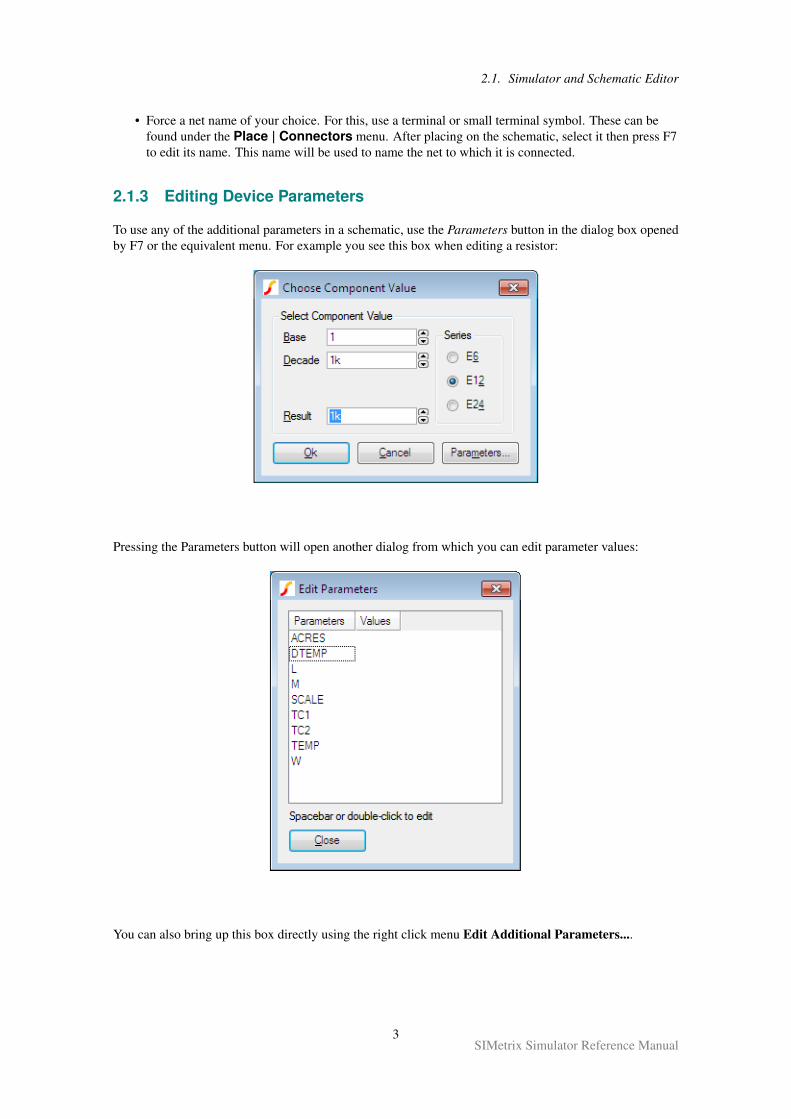
2.1.3 Editing Device Parameters
To use any of the additional parameters in a schematic, use the Parameters button in the dialog box openedby F7 or the equivalent menu. For example you see this box when editing a resistor:
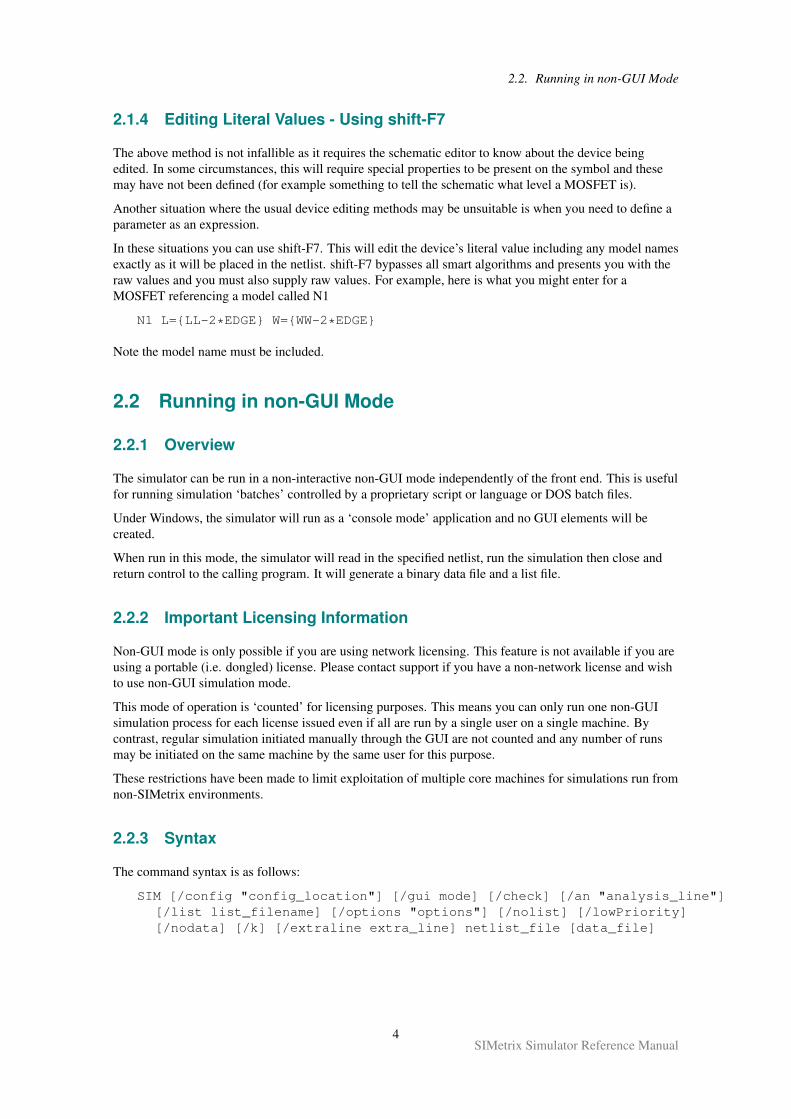
Pressing the Parameters button will open another dialog from which you can edit parameter values:
You can also bring up this box directly using the right click menu Edit Additional Parameters....
3SIMetrix Simulator Reference Manual
2.2. Running in non-GUI Mode
2.1.4 Editing Literal Values - Using shift-F7
The above method is not infallible as it requires the schematic editor to know about the device beingedited. In some circumstances, this will require special properties to be present on the symbol and thesemay have not been defined (for example something to tell the schematic what level a MOSFET is).
Another situation where the usual device editing methods may be unsuitable is when you need to define aparameter as an expression.
In these situations you can use shift-F7. This will edit the device’s literal value including any model namesexactly as it will be placed in the netlist. shift-F7 bypasses all smart algorithms and presents you with theraw values and you must also supply raw values. For example, here is what you might enter for aMOSFET referencing a model called N1
N1 L=LL-2*EDGE W=WW-2*EDGE
Note the model name must be included.
2.2 Running in non-GUI Mode
2.2.1 Overview
The simulator can be run in a non-interactive non-GUI mode independently of the front end. This is usefulfor running simulation ‘batches’ controlled by a proprietary script or language or DOS batch files.
Under Windows, the simulator will run as a ‘console mode’ application and no GUI elements will becreated.
When run in this mode, the simulator will read in the specified netlist, run the simulation then close andreturn control to the calling program. It will generate a binary data file and a list file.
2.2.2 Important Licensing Information
Non-GUI mode is only possible if you are using network licensing. This feature is not available if you areusing a portable (i.e. dongled) license. Please contact support if you have a non-network license and wishto use non-GUI simulation mode.
This mode of operation is ‘counted’ for licensing purposes. This means you can only run one non-GUIsimulation process for each license issued even if all are run by a single user on a single machine. Bycontrast, regular simulation initiated manually through the GUI are not counted and any number of runsmay be initiated on the same machine by the same user for this purpose.
These restrictions have been made to limit exploitation of multiple core machines for simulations run fromnon-SIMetrix environments.
2.2.3 Syntax
The command syntax is as follows:
SIM [/config "config_location"] [/gui mode] [/check] [/an "analysis_line"][/list list_filename] [/options "options"] [/nolist] [/lowPriority][/nodata] [/k] [/extraline extra_line] netlist_file [data_file]
4SIMetrix Simulator Reference Manual
2.2. Running in non-GUI Mode
config_location Location of file holding configuration settings. Configuration settingsinclude global options and global model library locations. The value mustbe of the form:
PATH;pathname
pathname may use system symbolic path values such as %EXEPATH%.See User’s Manual/Sundry Topics/Symbolic Path Names fordetails.
If not specified, the configuration settings will be taken from theBase.sxprj file. See the User’s Manual/Sundry Topics/ConfigurationSettings/Default Configuration Location for details on where this file islocated.
Alternatively, you can specify the location using a setting in the startup.inifile. Add a value called SimConfig to the [Startup] section and give it avalue of:
PATH;pathname
The startup.ini file must be located in the same directory as the SIMetrixexecutable binary. (SIMetrix.exe on Windows). See User’sManual/Sundry Topics/SIMetrix Command Line Parameters/Usingstartup.ini for more information on the startup.ini file.
Note that the /config switch if present must always appear before the firstargument to the command.
mode Mode of operation. Default = -1. Valid values are -1, 0, 1 and 2 but only -1and 1 are meaningful for stand-alone operation. 0 and 2 are used whenstarting the simulator process from the front end. -1 (same as omitting/gui) runs the simulator in console mode with all messages output to theconsole or terminal window. 1 enables GUI mode where the simulatorruns in a stand-alone mode but displays a graphical status box showingmessages and simulator progress. This mode is used by the‘asynchronous’ menus in the front end.
analysis_line If /an switch is specified, analysis_line specifies the analysis to beperformed and overrides all analysis lines specified in the netlist.
list_filename Name of list file. Default is main netlist file name with extension .OUT.Enclose path name in quotes if it contains spaces.
options List of options valid for .OPTIONS statement.
netlist_file File name of netlist.
data_file File to receive binary data output.
/check If specified, the netlist will be read in and parsed but no simulation will berun. Used to check syntax
/nolist If specified, no list file will be created
/lowPriority If specified, the simulator will be run as a low priority process, i.e. in thebackground. Recommended for long runs.
/nodata Only vectors explicitly specified using .KEEP or .PRINT will be output tothe binary file. Equivalent to ‘.KEEP /nov /noi /nodig’ in thenetlist.
5SIMetrix Simulator Reference Manual
2.3. Configuration Settings
/k If specified, the program will not finally terminate until the user haspressed enter and a message to that effect will be displayed. UnderWindows, if the program is not called from the DOS prompt but fromanother program, a console will be created for receiving messages. Theconsole will close when the program exits sometimes before the user hashad a chance to read the messages. This switch delays the exit of theprogram and hence the destruction of the console.
extra_line An additional line that will be appended to the netlist. This permits simplecustomisation of the netlist. This should be enclosed in double quotationmarks if the line has spaces.
2.2.4 Aborting
Press cntrl-C - you will be asked to confirm. The simulation will be paused while waiting for yourresponse and will continue if you enter ‘No’. This is an effective means of pausing the run if you needCPU cycles for another task, or you wish to copy the data file. See “Reading Data” on page 6.
2.2.5 Reading Data
A data file will be created for the simulation results as normal (see “The Binary Data File” on page 12).You can read this file after the simulation is complete use the SIMetrix menu File | Data | Load... . Youmay also read this data file while the simulation is running but you must pause the simulation first usingcntrl-C.
Important: if you read the data file before the simulation is complete or aborted, the file entries thatprovide the size of each vector will not have been filled. This means that the waveform viewer will have toscan the whole file in order to establish the size of the vectors. This could take a considerable time if thedata file is large.
2.3 Configuration Settings
Configuration settings consist of a number of persistent global options as well as the locations for installedmodel libraries.
When the simulator is run in GUI mode, its configuration settings are controlled by the front end andstored wherever the front end’s settings are stored. See the User’s Manual for more details.
The settings when run in non-GUI mode are stored in a configuration file which in fact defaults to thesame location as the default location for the front end’s settings. You can change this location using the/config switch detailed in “Running in non-GUI Mode” on page 4.
The format of the configuration file is:
[Options]option_settings
[Models]model_libraries
Where:
option_settings These are of the form name=value and specify a number of global settings.Boolean values are of the form name= without a value. If the entry ispresent it is TRUE if absent it is FALSE. Available global settings aredetailed below.
6SIMetrix Simulator Reference Manual
2.3. Configuration Settings
model_libraries A list of entries specifying search locations for model libraries. These areof the form name=value where name is a string and value is a searchlocation. The string used for name is arbitrary but must be unique. Entriesare sorted alphabetically according to the name and used to determine thesearch order. value is a path name and may contain wildcards (i.e. ‘*’ and‘?’).
2.3.1 Global Settings
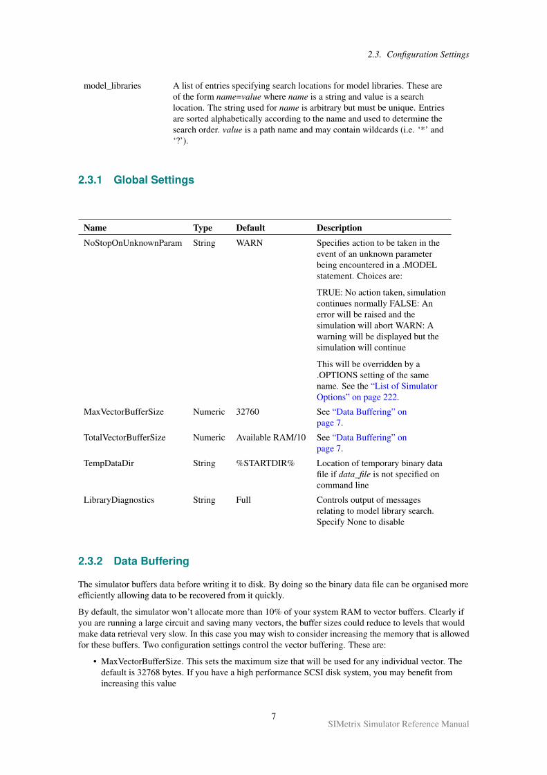
Name Type Default Description
NoStopOnUnknownParam String WARN Specifies action to be taken in theevent of an unknown parameterbeing encountered in a .MODELstatement. Choices are:
TRUE: No action taken, simulationcontinues normally FALSE: Anerror will be raised and thesimulation will abort WARN: Awarning will be displayed but thesimulation will continue
This will be overridden by a.OPTIONS setting of the samename. See the “List of SimulatorOptions” on page 222.
MaxVectorBufferSize Numeric 32760 See “Data Buffering” onpage 7.
TotalVectorBufferSize Numeric Available RAM/10 See “Data Buffering” onpage 7.
TempDataDir String %STARTDIR% Location of temporary binary datafile if data_file is not specified oncommand line
LibraryDiagnostics String Full Controls output of messagesrelating to model library search.Specify None to disable
2.3.2 Data Buffering
The simulator buffers data before writing it to disk. By doing so the binary data file can be organised moreefficiently allowing data to be recovered from it quickly.
By default, the simulator won’t allocate more than 10% of your system RAM to vector buffers. Clearly ifyou are running a large circuit and saving many vectors, the buffer sizes could reduce to levels that wouldmake data retrieval very slow. In this case you may wish to consider increasing the memory that is allowedfor these buffers. Two configuration settings control the vector buffering. These are:
• MaxVectorBufferSize. This sets the maximum size that will be used for any individual vector. Thedefault is 32768 bytes. If you have a high performance SCSI disk system, you may benefit fromincreasing this value
7SIMetrix Simulator Reference Manual
2.4. Netlist Format
• TotalVectorBufferSize. This sets the maximum amount of memory in bytes used for all buffers. Itdefaults to a value equal to 10% of your system RAM. This is usually sufficient for mostapplications but if you are simulating a very large circuit and have sufficient RAM you may like toincrease this value
The disk will not be written to until the buffers are full. With an all analog circuit all the buffers reach theirfull state at the same time so they all get written to disk at the same time. If you have 2G of RAM and aresimulating a large circuit, approximately 200M of data will be written to the disk at regular intervals. Thiswill result in a pause in the simulation coupled with a great deal of disk activity.
Note that both MaxVectorBufferSize and TotalVectorBufferSize may be set from the front end using theSet command. See User’s Manual/Sundry Topics/Using the Set and Unset Commands for details.
2.4 Netlist Format
The SIMetrix netlist format follows the general format used for all SPICE and SPICE compatiblesimulators. However, with so many SPICE derivatives and with two significantly different versions ofSPICE itself (SPICE 2 and SPICE 3) it is not possible to define a standard SPICE format. SIMetrix hasbeen developed to be as compatible as possible with model libraries that can be obtained from externalsources. For discrete devices, models are usually SPICE 2 compatible but some use extensions originallydeveloped for PSpice®. IC designers usually receive model files from fabrication companies and these areavailable for a variety of simulators usually including Hspice®. SIMetrix is compatible with all of thesebut simultaneous compatibility with all formats is not technically possible due to a small number of syntaxdetails - such as the character used for in line comments. To overcome these minor difficulties, a languagedeclaration can be placed at the top of the netlist and any file included using .INC or the Hspice® variantof .LIB. This is described in the following sections.
2.4.1 File Format
A complete netlist consists of:
• A title line
• Optional language declaration
• Device lines
• Statement lines
• Comment lines
The title line must be the first line of the file and may be empty. The remaining lines - with someexceptions - may be placed in any order
All other lines are defined by their first non-whitespace character as follows.
• Statement lines begin with a period: ‘.’
• Comment lines begin with an asterix: ‘*’
• Device lines begin with a letter
A line is usually terminated with a new line character but may be continued using the ‘+’ continuationcharacter. So if the first non-whitespace character is a ‘+’ the line will be considered to be an extension ofthe previous line. SPICE requires the ‘+’ to be the first character, SIMetrix allows whitespace (space ortab) to precede it.
8SIMetrix Simulator Reference Manual
2.4. Netlist Format
2.4.2 Language Declaration
SIMetrix is able to read PSpice®, Hspice® and native SIMetrix netlists, but in some cases needs to beinstructed what format netlist it is reading. Currently there are three areas where simultaneouscompatibility has not been possible. These are:
• Inline comment character.
• Unlabelled device parameters
• The meaning of LOG() and PWR() functions
SIMetrix can be instructed to use any of the three languages by using the language declaration. This is oneof:
*#SIMETRIX *#HSPICE *#PSPICE
The language declaration must be placed at the top of the file immediately below the title line. It can alsobe placed in files referenced using .INC or the HSPICE® version of .LIB in which case it will apply only tothat file and any others that it calls. A language declaration placed anywhere else in a file will be ignored.
For details see “Language Differences” on page 33.
The *#SIMETRIX language declaration can also be supplied with a parameter to specify the separatorletter used for devices. See “Device Lines” on page 9 section for details.
2.4.3 Comments
Any line other than a language declaration beginning with a ‘*’ is defined as a comment and will beignored. Also anything between a semi-colon ‘;’ (‘$’ in HSPICE mode) and the end of the line will betreated as comment and will also be ignored. Some SPICE simulators require the ‘*’ character to be thefirst character of the line. SIMetrix allows it to be preceded by white space (spaces and tabs).
2.4.4 Device Lines
Device lines usually follow the following basic form but each type of device tends to have its own nuances:
Name nodelist value [parameters]
value may be an actual number e.g. in the case of passive components such as resistors, or it may be amodel name in the case of semiconductor devices such as bipolar transistors. Models are defined using a.MODEL statement line.
nodelist is a list of netnames. The number and order of these is device dependent. The netname itself mayconsist of any collection of non-control ASCII characters except whitespace and ‘.’. All other ASCIIcharacters are accepted although it is suggested that the following characters are avoided if possible:
\ " \% \& + - * / ^ < > [ ] ' @
If any of these characters are used in a netname, a special syntax will be needed to plot any signal voltageon that net. This is explained in “Output Data Names” on page 12. In addition the characters ‘[’, ‘]’, ‘%’,‘!’ and ‘ ’ have a special meaning when used with XSPICE devices and therefore should be avoided at alltimes.
The name is the circuit reference of the device. The first letter of this name determines the type of deviceas shown in the table below.
The Pin Names column in the following table is relevant to the vector name used for values of device pincurrent. See “Output Data Names” on page 12.
9SIMetrix Simulator Reference Manual
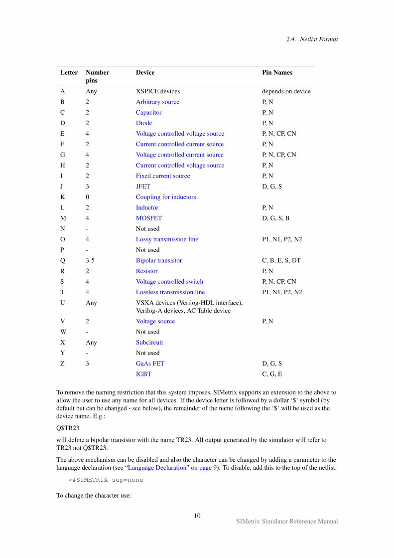
2.4. Netlist Format
Letter Numberpins
Device Pin Names
A Any XSPICE devices depends on device
B 2 Arbitrary source P, N
C 2 Capacitor P, N
D 2 Diode P, N
E 4 Voltage controlled voltage source P, N, CP, CN
F 2 Current controlled current source P, N
G 4 Voltage controlled current source P, N, CP, CN
H 2 Current controlled voltage source P, N
I 2 Fixed current source P, N
J 3 JFET D, G, S
K 0 Coupling for inductors
L 2 Inductor P, N
M 4 MOSFET D, G, S, B
N - Not used
O 4 Lossy transmission line P1, N1, P2, N2
P - Not used
Q 3-5 Bipolar transistor C, B, E, S, DT
R 2 Resistor P, N
S 4 Voltage controlled switch P, N, CP, CN
T 4 Lossless transmission line P1, N1, P2, N2
U Any VSXA devices (Verilog-HDL interface),Verilog-A devices, AC Table device
V 2 Voltage source P, N
W - Not used
X Any Subcircuit
Y - Not used
Z 3 GaAs FET D, G, S
IGBT C, G, E
To remove the naming restriction that this system imposes, SIMetrix supports an extension to the above toallow the user to use any name for all devices. If the device letter is followed by a dollar ‘$’ symbol (bydefault but can be changed - see below), the remainder of the name following the ‘$’ will be used as thedevice name. E.g.:
Q$TR23
will define a bipolar transistor with the name TR23. All output generated by the simulator will refer toTR23 not Q$TR23.
The above mechanism can be disabled and also the character can be changed by adding a parameter to thelanguage declaration (see “Language Declaration” on page 9). To disable, add this to the top of the netlist:
*#SIMETRIX sep=none
To change the character use:
10SIMetrix Simulator Reference Manual
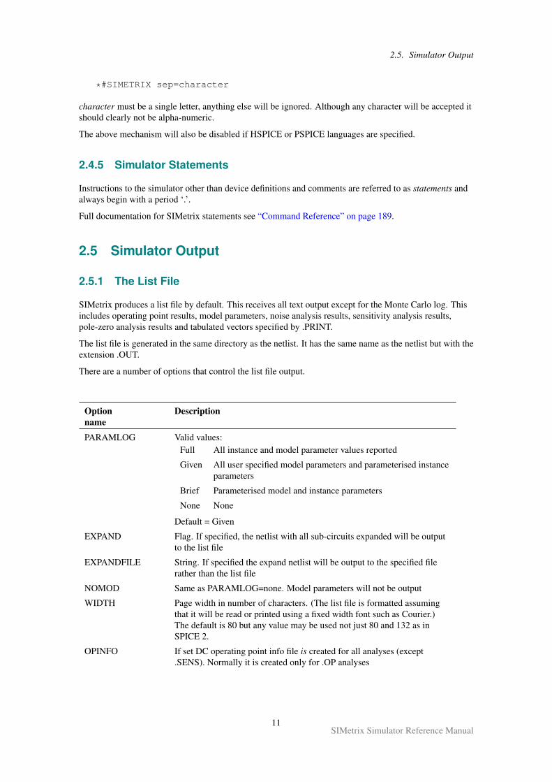
2.5. Simulator Output
*#SIMETRIX sep=character
character must be a single letter, anything else will be ignored. Although any character will be accepted itshould clearly not be alpha-numeric.
The above mechanism will also be disabled if HSPICE or PSPICE languages are specified.
2.4.5 Simulator Statements
Instructions to the simulator other than device definitions and comments are referred to as statements andalways begin with a period ‘.’.
Full documentation for SIMetrix statements see “Command Reference” on page 189.
2.5 Simulator Output
2.5.1 The List File
SIMetrix produces a list file by default. This receives all text output except for the Monte Carlo log. Thisincludes operating point results, model parameters, noise analysis results, sensitivity analysis results,pole-zero analysis results and tabulated vectors specified by .PRINT.
The list file is generated in the same directory as the netlist. It has the same name as the netlist but with theextension .OUT.
There are a number of options that control the list file output.
Optionname
Description
PARAMLOG Valid values:Full All instance and model parameter values reported
Given All user specified model parameters and parameterised instanceparameters
Brief Parameterised model and instance parameters
None None
Default = Given
EXPAND Flag. If specified, the netlist with all sub-circuits expanded will be outputto the list file
EXPANDFILE String. If specified the expand netlist will be output to the specified filerather than the list file
NOMOD Same as PARAMLOG=none. Model parameters will not be output
WIDTH Page width in number of characters. (The list file is formatted assumingthat it will be read or printed using a fixed width font such as Courier.)The default is 80 but any value may be used not just 80 and 132 as inSPICE 2.
OPINFO If set DC operating point info file is created for all analyses (except.SENS). Normally it is created only for .OP analyses
11SIMetrix Simulator Reference Manual
2.5. Simulator Output
2.5.2 The Binary Data File
The simulation data is stored in a binary data file. The format is proprietary to SIMetrix and is notcompatible with SPICE ‘raw’ files.
The name and location of the binary file depends on configuration settings and in what mode the simulatoris run. Usually, the file is located in the directory specified by the TEMPDATADIR configuration setting(see “Configuration Settings” on page 6) and is named according to the analysis type and appended withthe extension .sxdat. E.g.tran1.sxdat, ac2.sxdat, dc3.sxdat etc. The name and location can be overridden atthe program command line if operated in non-GUI mode or at the front end Run command line if run inGUI mode.
Only the SIMetrix front end can read the simulator’s binary data file. When run in GUI mode, the file isautomatically loaded and in fact it is not usually necessary to know anything about it except perhaps whenit grows very large and fills up your disk. If the simulator is run in non-GUI mode, it becomes necessary toexplicitly load the data into the front end when the run is complete. This can be done with the commandshell menu File | Data | Load.... After the data is loaded, the results can be plotted in the usual manner.See User’s Manual/Graphs,Probes and Data Analysis/Saving Data/Restoring Simulation Data for furtherdetails.
2.5.3 Output Data Names
For transient, DC and AC analyses, SIMetrix calculates and stores the circuit’s node voltages and devicepin currents and these are all given unique names. If using probing techniques with the front end’sschematic editor you don’t usually need to know anything about the names used. However there aresituations where it is necessary or helpful to know how these names are derived. An example is whencompiling an expression relating voltages and currents to be used in a .PRINT statement. Another is whenplotting results created by simulating a netlist that was not generated using the schematic editor. Thenames used are documented in the following notes.
Top Level Node Voltages
The vector names used for node voltages at the top level (i.e. not in a subcircuit) are simply the name ofthe node used in the netlist.
Subcircuit Node Voltages
For nodes within a subcircuit, the name is prefixed with the subcircuit reference and a ‘.’. For example:
X1 N1 N2 N3 SubNameX2 N4 N5 N6 SubName
.SUBCKT 1 2 3 SubNameX3 N1 2 N3 SubName2R1 VIN 0 1k....ENDS
.SUBCKT 1 2 3 SubName2V1 VCC 0 5....ENDS
12SIMetrix Simulator Reference Manual
2.5. Simulator Output
The internal node VIN in definition SubName referenced by X1 would be called X1.VIN. The same nodereferenced by X2 would be called X2.VIN. The node VCC defined in subcircuit SubName2 would benamed X1.X3.VCC and X2.X3.VCC for X1 and X2 respectively.
Nodes with Non-standard Names
A non-standard node name is one that begins with a digit or which contains one or more of the characters:
\ " \% \& + - * / ^ < > [ ] ' @
These are legal but introduce problems when accessing the voltage data that they carry. The abovecharacters can be used in arithmetic expressions so cause a conflict if used as a node name. In order toaccess the voltage data on a node so named, use the Vec() function:
Vec(’node_name’)
Example with .PRINT and node called V+
.PRINT TRAN Vec('V+')
A similar syntax is required when using the front end plotting commands.
Device Pin Currents
Device pin currents are named in the following form:
device_name#pin_name
For primitive devices (i.e. not sub-circuits) pin_name must comply with the table in “Device Lines” onpage 9. For example the current into the collector of Q23 would be Q23#c.
The pin names for sub-circuits depend on whether the pinnames: specifier (see “Subcircuit Instance” onpage 108) is included in the netlist entry for the device. If it is the pin current name will be the name listedafter pinnames:. If it isn’t then they are numbered in sequence starting from 1. The order is the same as theorder they appear in the netlist device line. For example, if the subcircuit line is:
X$U10 N1 N2 N3 N4 N5 LM324 pinnames: VINP VINN VP VN VOUT
The current into the last pin (connected to N5) would be U10#VOUT
(Note that ‘X$’ is stripped off as explained above in “Device Lines” on page 9).
If the netlist line is:
X$U10 N1 N2 N3 N4 N5 LM324
The same current would be U10#5
Internal Device Values
Some devices have internal nodes or sources and the voltages or currents associated with these may beoutput by the simulator. These are named in a similar manner to pin currents i.e.
device_name#internal_name
The internal_name depends on the device. For example, bipolar transistors create an internal node for eachterminal that specifies a corresponding resistance parameter. So if the RE parameter is specified an internalnode will be created called emitter.
Note that internal device values are only output if explicitly enabled using the “.KEEP /INTERNAL”statement. See “.KEEP” on page 206.
13SIMetrix Simulator Reference Manual

2.6. Controlling Data Saved
2.6 Data Handling - Controlling Data Saved
As explained in “The Binary Data File” on page 12, all data is saved to a binary disk file. By default, allsignals visible in a schematic are saved. That is all signals at the top level of a hierarchy and in all childschematics are saved. Signals inside subcircuits that were not generated by a hierarchical schematic arenot saved.
SIMetrix has comprehensive features for changing exactly what data is saved. Some simulations cangenerate huge amounts of data and with multi-core multi-step simulations, the rate at which the data iscreated can exceed the performance of the disk system. It is therefore desirable in some cases to reduce theamount of data saved.
For simulations run from the user interface, some of the data handling features are available through theGUI. See User’s Manual/Analysis Modes/Data Handling and Keeps.
More comprehensive features are available using .KEEP and .OPTIONS. See “.KEEP” on page 206 forfull details.
14SIMetrix Simulator Reference Manual
Chapter 3
Simulator Devices
3.1 Overview
This chapter is an introduction to the “Analog Deivce reference” on page 38 and the “Digital/Mixed SignalDevice Reference” on page 134.
The device reference chapters describe all simulator devices at the netlist level. The netlist consists of a listof component definitions, along with simulator commands, which the simulator can understand. Simplecomponents, such as resistors just need a value to define them. Other more complicated devices such astransistors need a number of parameters to describe their characteristics.
The device references includes details of all device and model parameters. Using the schematic editor andmodel library you may not often need to read this section. Some of the devices, however, have advancedoptions not directly supported by the user interface. For example, many devices allow a local temperatureto be specified. This requires the component value to be appended with TEMP=.... This device parameterand others are documented here.
Note that many parts either supplied with SIMetrix or available from component manufacturers areimplemented as subcircuits. These are circuit designs to simulate the behaviour of high level devices suchas opamps. SIMetrix (and all other SPICE simulators) do not have an opamp device built in but use thesemacro models instead. Full documentation for these devices is beyond the scope of this manual but cansometimes be obtained from their suppliers.
3.2 Using XSPICE Devices
Some devices are implemented as part of the XSPICE ‘code modelling’ framework. This frameworkintroduces some new features at the netlist level not supported by standard SPICE devices. These newfeatures are described in this section.
All but one of these devices that use this framework are digital or mixed signal devices and the referencefor these can be found at “Digital/Mixed Signal Device Reference” on page 134.
The exception is the “S-domain Transfer Function Block” on page 73 which is a pure analog part.
3.2.1 Vector Connections
Some models feature an arbitrary number of inputs or/and outputs. For example, an AND gate can haveany number of inputs. It would be inflexible to have a separate model for every configuration of AND gateso a method of grouping connections together has been devised. These are known as vector connections.Vector connections are enclosed in square brackets. E.g. the netlist entry for an AND gate is:
15SIMetrix Simulator Reference Manual
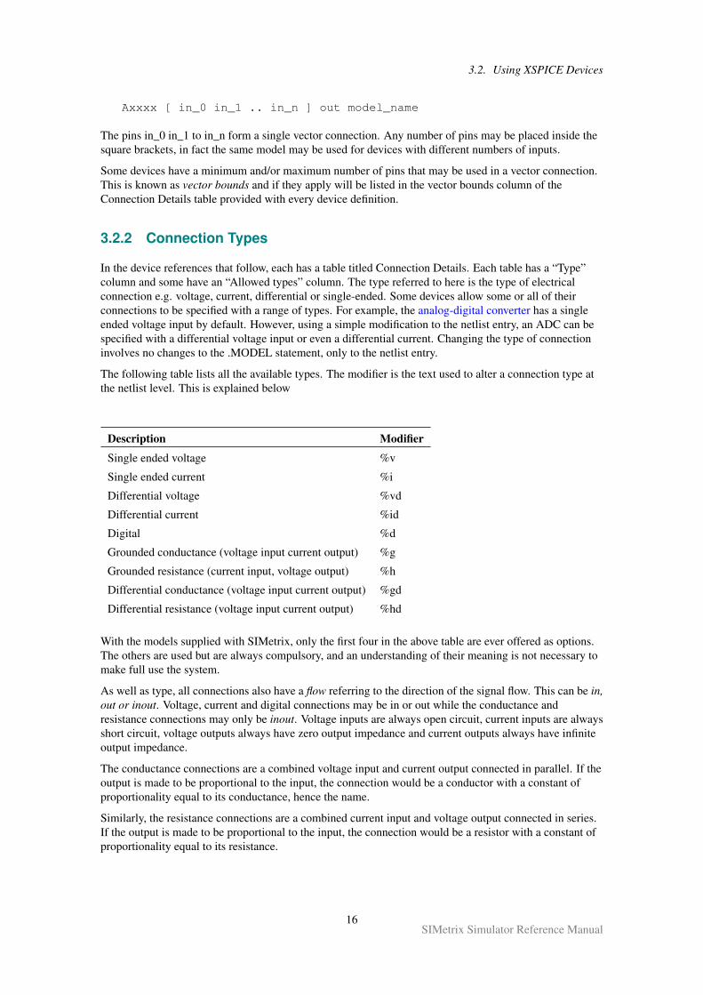
3.2. Using XSPICE Devices
Axxxx [ in_0 in_1 .. in_n ] out model_name
The pins in_0 in_1 to in_n form a single vector connection. Any number of pins may be placed inside thesquare brackets, in fact the same model may be used for devices with different numbers of inputs.
Some devices have a minimum and/or maximum number of pins that may be used in a vector connection.This is known as vector bounds and if they apply will be listed in the vector bounds column of theConnection Details table provided with every device definition.
3.2.2 Connection Types
In the device references that follow, each has a table titled Connection Details. Each table has a “Type”column and some have an “Allowed types” column. The type referred to here is the type of electricalconnection e.g. voltage, current, differential or single-ended. Some devices allow some or all of theirconnections to be specified with a range of types. For example, the analog-digital converter has a singleended voltage input by default. However, using a simple modification to the netlist entry, an ADC can bespecified with a differential voltage input or even a differential current. Changing the type of connectioninvolves no changes to the .MODEL statement, only to the netlist entry.
The following table lists all the available types. The modifier is the text used to alter a connection type atthe netlist level. This is explained below
Description Modifier
Single ended voltage %v
Single ended current %i
Differential voltage %vd
Differential current %id
Digital %d
Grounded conductance (voltage input current output) %g
Grounded resistance (current input, voltage output) %h
Differential conductance (voltage input current output) %gd
Differential resistance (voltage input current output) %hd
With the models supplied with SIMetrix, only the first four in the above table are ever offered as options.The others are used but are always compulsory, and an understanding of their meaning is not necessary tomake full use the system.
As well as type, all connections also have a flow referring to the direction of the signal flow. This can be in,out or inout. Voltage, current and digital connections may be in or out while the conductance andresistance connections may only be inout. Voltage inputs are always open circuit, current inputs are alwaysshort circuit, voltage outputs always have zero output impedance and current outputs always have infiniteoutput impedance.
The conductance connections are a combined voltage input and current output connected in parallel. If theoutput is made to be proportional to the input, the connection would be a conductor with a constant ofproportionality equal to its conductance, hence the name.
Similarly, the resistance connections are a combined current input and voltage output connected in series.If the output is made to be proportional to the input, the connection would be a resistor with a constant ofproportionality equal to its resistance.
16SIMetrix Simulator Reference Manual
3.3. Using Expressions
Changing Connection Type
If a model allows one or more of its connections to be given a different type, this can be done by precedingthe connection entry with the appropriate modifier listed in the table above. For example if you wish tospecify a 4 bit ADC with a differential voltage input, the netlist entry would be something like:
A1 %vd ANALOG_INP ANALOG_INN CLOCK_IN [ DATA_OUT_0 DATA_OUT_1 DATA_OUT_2DATA_OUT_3 ] DATA_VALID ADC_4
3.3 Using Expressions
3.3.1 Overview
Expressions consist of arithmetic operators, functions, variables and constants and may be employed in thefollowing locations:
• As device parameters
• As model parameters
• To define a variable (see “.PARAM” on page 239) which can itself be used in an expression.
• As the governing expression used for arbitrary sources.
They have a wide range of uses. For example:
• To define a number of device or model parameters that depend on some common characteristic. Thiscould be a circuit specification such as the cut-off frequency of a filter or maybe a physicalcharacteristic to define a device model.
• To define tolerances used in Monte Carlo analyses.
• Used with an arbitrary source, to define a non-linear device.
3.3.2 Using Expressions for Device Parameters
Device or instance parameters are placed on the device line. For example the length parameter of aMOSFET, L, is a device parameter. A MOSFET line with constant parameters might be:
M1 1 2 3 4 MOS1 L=1u W=2u
L and W could be replaced by expressions. For example:
M1 1 2 3 4 MOS1 L=LL-2*EDGE W=WW-2*EDGE
Device parameter expressions must usually be enclosed with either single quotation marks ( ’ ) doublequotation marks ( " ) or braces ( ‘’ and ‘’ ). The expression need not be so enclosed if it consists of a singlevariable. For example:
.PARAM LL=2u WW=1uM1 1 2 3 4 MOS1 L=LL W=WW
3.3.3 Using Expressions for Model Parameters
The rules for using expressions for device parameters also apply to model parameters. E.g.
.MODEL N1 NPN IS=is BF=beta*1.3
17SIMetrix Simulator Reference Manual
3.3. Using Expressions
3.3.4 Expression Syntax
Expressions generally comprise the following elements:
• Circuit variables
• Parameters
• Constants.
• Operators
• Functions
• Look up tables
These are described in the following sections.
Circuit Variables
Circuit variables may only be used in expressions used to define “arbitrary sources” on page 39 and todefine variables that themselves are accessed only in arbitrary source expressions.
Circuit variables allow an expression to reference voltages and currents in any part of the circuit beingsimulated.
Voltages are of the form:
V(node_name1)
OR
V(node_name1, node_name2)
Where node_name1 and node_name2 are the name of the node carrying the voltage of interest. Thesecond form above returns the difference between the voltages on node_name1 and node_name2. If usingthe schematic editor nodenames are normally allocated by the netlist generator. For information on how todisplay and edit the schematic’s node names, refer to “Displaying Net and Pin Names” on page 2.
Currents are of the form:
I(source_name)
Where source_name is the name of a voltage source carrying the current of interest. The source may be afixed voltage source, a current controlled voltage source, a voltage controlled voltage source or an arbitraryvoltage source. It is legal for an expression used in an arbitrary source to reference itself e.g.:
B1 n1 n2 V=100*I(B1)
Implements a 100 ohm resistor.
Parameters
These are defined using the .PARAM statement. For example:
.PARAM res=100B1 n1 n2 V=res*I(B1)
Also implements a 100 ohm resistor.
Circuit variables may be used .PARAM statements, for example:
18SIMetrix Simulator Reference Manual
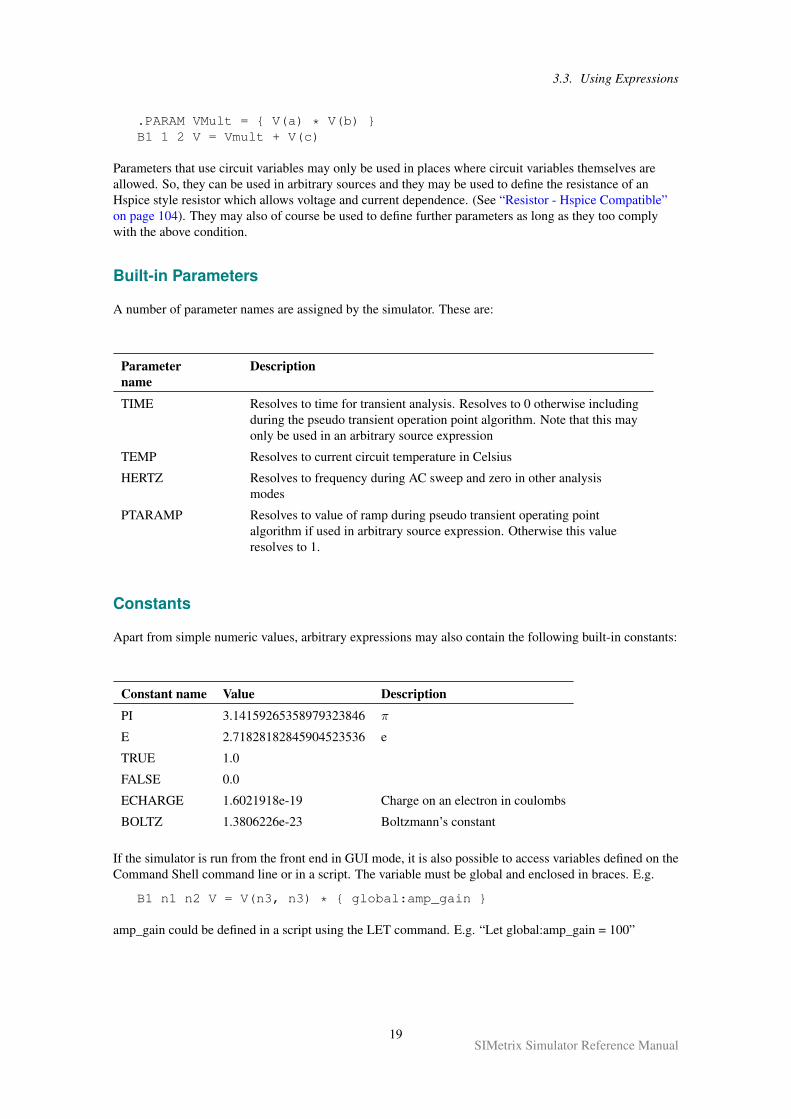
3.3. Using Expressions
.PARAM VMult = V(a) * V(b) B1 1 2 V = Vmult + V(c)
Parameters that use circuit variables may only be used in places where circuit variables themselves areallowed. So, they can be used in arbitrary sources and they may be used to define the resistance of anHspice style resistor which allows voltage and current dependence. (See “Resistor - Hspice Compatible”on page 104). They may also of course be used to define further parameters as long as they too complywith the above condition.
Built-in Parameters
A number of parameter names are assigned by the simulator. These are:
Parametername
Description
TIME Resolves to time for transient analysis. Resolves to 0 otherwise includingduring the pseudo transient operation point algorithm. Note that this mayonly be used in an arbitrary source expression
TEMP Resolves to current circuit temperature in Celsius
HERTZ Resolves to frequency during AC sweep and zero in other analysismodes
PTARAMP Resolves to value of ramp during pseudo transient operating pointalgorithm if used in arbitrary source expression. Otherwise this valueresolves to 1.
Constants
Apart from simple numeric values, arbitrary expressions may also contain the following built-in constants:
Constant name Value Description
PI 3.14159265358979323846 π
E 2.71828182845904523536 e
TRUE 1.0
FALSE 0.0
ECHARGE 1.6021918e-19 Charge on an electron in coulombs
BOLTZ 1.3806226e-23 Boltzmann’s constant
If the simulator is run from the front end in GUI mode, it is also possible to access variables defined on theCommand Shell command line or in a script. The variable must be global and enclosed in braces. E.g.
B1 n1 n2 V = V(n3, n3) * global:amp_gain
amp_gain could be defined in a script using the LET command. E.g. “Let global:amp_gain = 100”
19SIMetrix Simulator Reference Manual
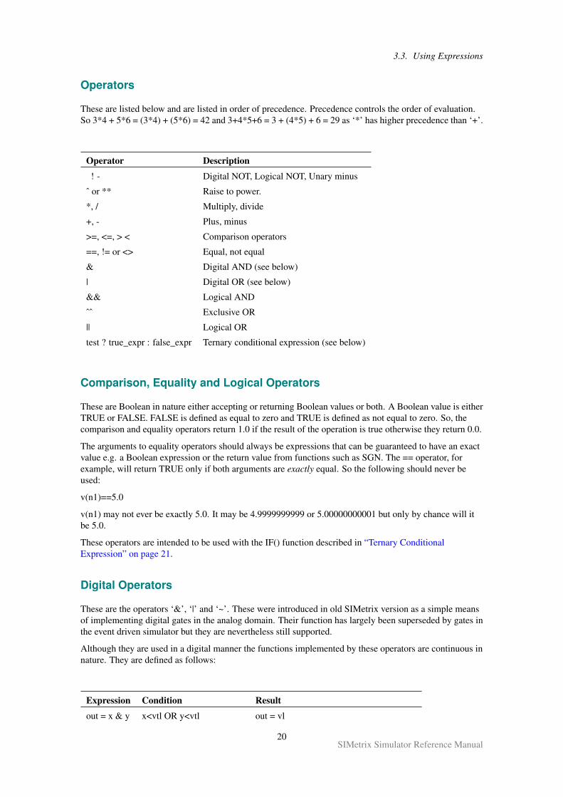
3.3. Using Expressions
Operators
These are listed below and are listed in order of precedence. Precedence controls the order of evaluation.So 3*4 + 5*6 = (3*4) + (5*6) = 42 and 3+4*5+6 = 3 + (4*5) + 6 = 29 as ‘*’ has higher precedence than ‘+’.
Operator Description
! - Digital NOT, Logical NOT, Unary minus
ˆ or ** Raise to power.
*, / Multiply, divide
+, - Plus, minus
>=, <=, > < Comparison operators
==, != or <> Equal, not equal
& Digital AND (see below)
| Digital OR (see below)
&& Logical AND
ˆˆ Exclusive OR
|| Logical OR
test ? true_expr : false_expr Ternary conditional expression (see below)
Comparison, Equality and Logical Operators
These are Boolean in nature either accepting or returning Boolean values or both. A Boolean value is eitherTRUE or FALSE. FALSE is defined as equal to zero and TRUE is defined as not equal to zero. So, thecomparison and equality operators return 1.0 if the result of the operation is true otherwise they return 0.0.
The arguments to equality operators should always be expressions that can be guaranteed to have an exactvalue e.g. a Boolean expression or the return value from functions such as SGN. The == operator, forexample, will return TRUE only if both arguments are exactly equal. So the following should never beused:
v(n1)==5.0
v(n1) may not ever be exactly 5.0. It may be 4.9999999999 or 5.00000000001 but only by chance will itbe 5.0.
These operators are intended to be used with the IF() function described in “Ternary ConditionalExpression” on page 21.
Digital Operators
These are the operators ‘&’, ‘|’ and ‘~’. These were introduced in old SIMetrix version as a simple meansof implementing digital gates in the analog domain. Their function has largely been superseded by gates inthe event driven simulator but they are nevertheless still supported.
Although they are used in a digital manner the functions implemented by these operators are continuous innature. They are defined as follows:
Expression Condition Result
out = x & y x<vtl OR y<vtl out = vl
20SIMetrix Simulator Reference Manual
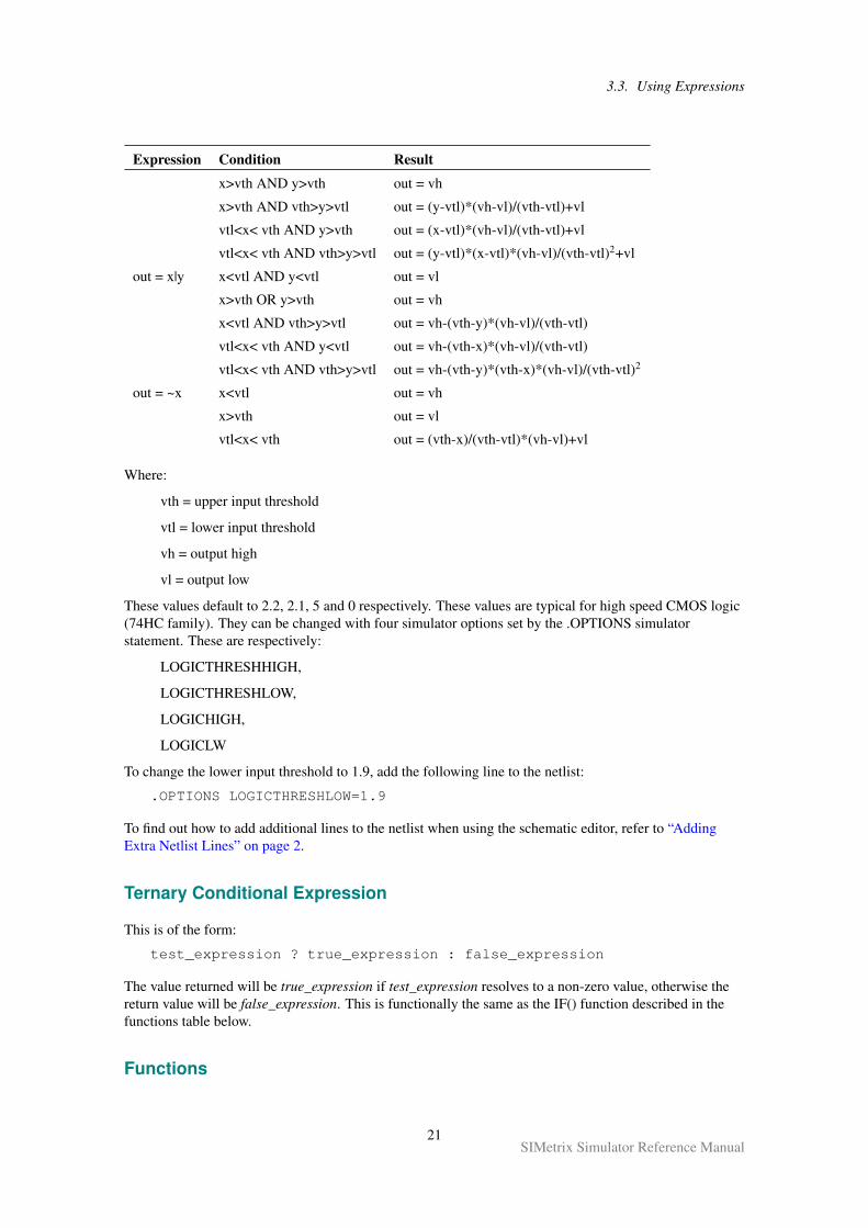
3.3. Using Expressions
Expression Condition Result
x>vth AND y>vth out = vh
x>vth AND vth>y>vtl out = (y-vtl)*(vh-vl)/(vth-vtl)+vl
vtl<x< vth AND y>vth out = (x-vtl)*(vh-vl)/(vth-vtl)+vl
vtl<x< vth AND vth>y>vtl out = (y-vtl)*(x-vtl)*(vh-vl)/(vth-vtl)2+vl
out = x|y x<vtl AND y<vtl out = vl
x>vth OR y>vth out = vh
x<vtl AND vth>y>vtl out = vh-(vth-y)*(vh-vl)/(vth-vtl)
vtl<x< vth AND y<vtl out = vh-(vth-x)*(vh-vl)/(vth-vtl)
vtl<x< vth AND vth>y>vtl out = vh-(vth-y)*(vth-x)*(vh-vl)/(vth-vtl)2
out = ~x x<vtl out = vh
x>vth out = vl
vtl<x< vth out = (vth-x)/(vth-vtl)*(vh-vl)+vl
Where:
vth = upper input threshold
vtl = lower input threshold
vh = output high
vl = output low
These values default to 2.2, 2.1, 5 and 0 respectively. These values are typical for high speed CMOS logic(74HC family). They can be changed with four simulator options set by the .OPTIONS simulatorstatement. These are respectively:
LOGICTHRESHHIGH,
LOGICTHRESHLOW,
LOGICHIGH,
LOGICLW
To change the lower input threshold to 1.9, add the following line to the netlist:
.OPTIONS LOGICTHRESHLOW=1.9
To find out how to add additional lines to the netlist when using the schematic editor, refer to “AddingExtra Netlist Lines” on page 2.
Ternary Conditional Expression
This is of the form:
test_expression ? true_expression : false_expression
The value returned will be true_expression if test_expression resolves to a non-zero value, otherwise thereturn value will be false_expression. This is functionally the same as the IF() function described in thefunctions table below.
Functions
21SIMetrix Simulator Reference Manual
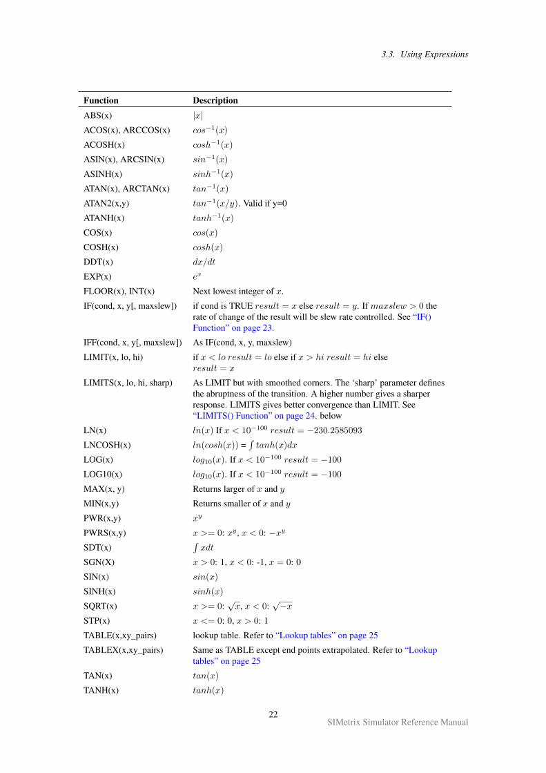
3.3. Using Expressions
Function Description
ABS(x) |x|ACOS(x), ARCCOS(x) cos−1(x)
ACOSH(x) cosh−1(x)
ASIN(x), ARCSIN(x) sin−1(x)
ASINH(x) sinh−1(x)
ATAN(x), ARCTAN(x) tan−1(x)
ATAN2(x,y) tan−1(x/y). Valid if y=0
ATANH(x) tanh−1(x)
COS(x) cos(x)
COSH(x) cosh(x)
DDT(x) dx/dt
EXP(x) ex
FLOOR(x), INT(x) Next lowest integer of x.
IF(cond, x, y[, maxslew]) if cond is TRUE result = x else result = y. If maxslew > 0 therate of change of the result will be slew rate controlled. See “IF()Function” on page 23.
IFF(cond, x, y[, maxslew]) As IF(cond, x, y, maxslew)
LIMIT(x, lo, hi) if x < lo result = lo else if x > hi result = hi elseresult = x
LIMITS(x, lo, hi, sharp) As LIMIT but with smoothed corners. The ‘sharp’ parameter definesthe abruptness of the transition. A higher number gives a sharperresponse. LIMITS gives better convergence than LIMIT. See“LIMITS() Function” on page 24. below
LN(x) ln(x) If x < 10−100 result = −230.2585093
LNCOSH(x) ln(cosh(x)) =∫tanh(x)dx
LOG(x) log10(x). If x < 10−100 result = −100
LOG10(x) log10(x). If x < 10−100 result = −100
MAX(x, y) Returns larger of x and y
MIN(x,y) Returns smaller of x and y
PWR(x,y) xy
PWRS(x,y) x >= 0: xy , x < 0: −xy
SDT(x)∫xdt
SGN(X) x > 0: 1, x < 0: -1, x = 0: 0
SIN(x) sin(x)
SINH(x) sinh(x)
SQRT(x) x >= 0:√x, x < 0:
√−x
STP(x) x <= 0: 0, x > 0: 1
TABLE(x,xy_pairs) lookup table. Refer to “Lookup tables” on page 25
TABLEX(x,xy_pairs) Same as TABLE except end points extrapolated. Refer to “Lookuptables” on page 25
TAN(x) tan(x)
TANH(x) tanh(x)
22SIMetrix Simulator Reference Manual
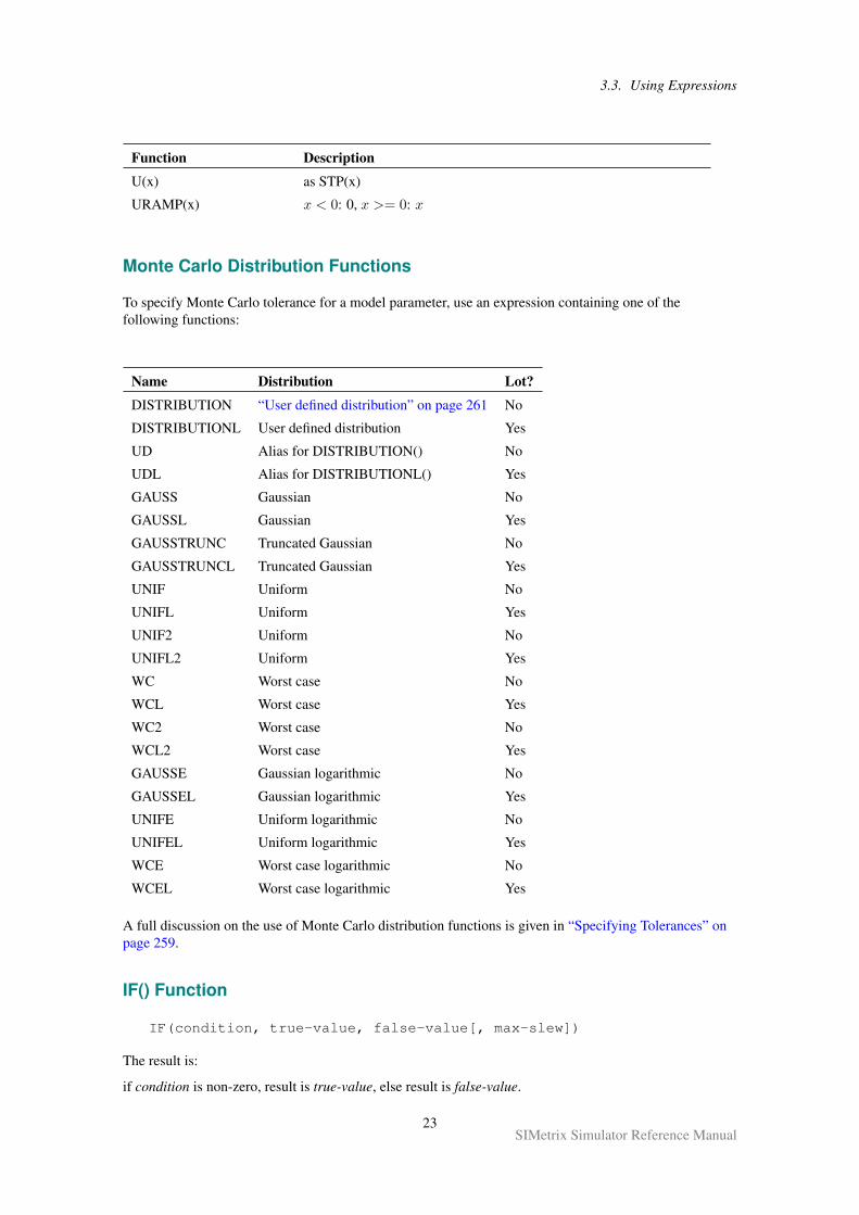
3.3. Using Expressions
Function Description
U(x) as STP(x)
URAMP(x) x < 0: 0, x >= 0: x
Monte Carlo Distribution Functions
To specify Monte Carlo tolerance for a model parameter, use an expression containing one of thefollowing functions:
Name Distribution Lot?
DISTRIBUTION “User defined distribution” on page 261 No
DISTRIBUTIONL User defined distribution Yes
UD Alias for DISTRIBUTION() No
UDL Alias for DISTRIBUTIONL() Yes
GAUSS Gaussian No
GAUSSL Gaussian Yes
GAUSSTRUNC Truncated Gaussian No
GAUSSTRUNCL Truncated Gaussian Yes
UNIF Uniform No
UNIFL Uniform Yes
UNIF2 Uniform No
UNIFL2 Uniform Yes
WC Worst case No
WCL Worst case Yes
WC2 Worst case No
WCL2 Worst case Yes
GAUSSE Gaussian logarithmic No
GAUSSEL Gaussian logarithmic Yes
UNIFE Uniform logarithmic No
UNIFEL Uniform logarithmic Yes
WCE Worst case logarithmic No
WCEL Worst case logarithmic Yes
A full discussion on the use of Monte Carlo distribution functions is given in “Specifying Tolerances” onpage 259.
IF() Function
IF(condition, true-value, false-value[, max-slew])
The result is:
if condition is non-zero, result is true-value, else result is false-value.
23SIMetrix Simulator Reference Manual
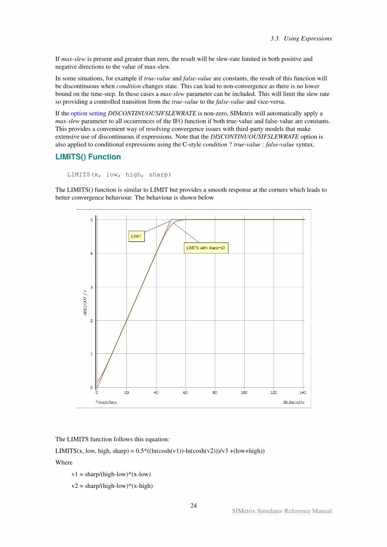
3.3. Using Expressions
If max-slew is present and greater than zero, the result will be slew-rate limited in both positive andnegative directions to the value of max-slew.
In some situations, for example if true-value and false-value are constants, the result of this function willbe discontinuous when condition changes state. This can lead to non-convergence as there is no lowerbound on the time-step. In these cases a max-slew parameter can be included. This will limit the slew rateso providing a controlled transition from the true-value to the false-value and vice-versa.
If the option setting DISCONTINUOUSIFSLEWRATE is non-zero, SIMetrix will automatically apply amax-slew parameter to all occurrences of the IF() function if both true-value and false-value are constants.This provides a convenient way of resolving convergence issues with third-party models that makeextensive use of discontinuous if expressions. Note that the DISCONTINUOUSIFSLEWRATE option isalso applied to conditional expressions using the C-style condition ? true-value : false-value syntax.
LIMITS() Function
LIMITS(x, low, high, sharp)
The LIMITS() function is similar to LIMIT but provides a smooth response at the corners which leads tobetter convergence behaviour. The behaviour is shown below
The LIMITS function follows this equation:
LIMITS(x, low, high, sharp) = 0.5*((ln(cosh(v1))-ln(cosh(v2)))/v3 +(low+high))
Where
v1 = sharp/(high-low)*(x-low)
v2 = sharp/(high-low)*(x-high)
24SIMetrix Simulator Reference Manual
3.3. Using Expressions
v3 = sharp/(high-low)
Look-up Tables
Expressions may contain any number of look-up tables. This allows a transfer function of a device to bespecified according to - say - measured values without having to obtain a mathematical equation. Look-uptables are specified in terms of x, y value pairs which describe a piece-wise linear transfer function. Thereare three ways to create a lookup table:
Method 1 Syntax in form: TABLE[xy_pairs](input_expression).
xy_pairs A sequence of comma separated pairs of constantvalues that define the input and output values of thetable. For each pair, the first value is the x or inputvalue and the second is the y or output value. Onlyexplicit numeric constants may be used. Eveninternal constants such as PI may not be used.
input_expression Expression defining the input or x value of thetable.
Method 2 Syntax in form: TABLE(input_expression, xy_pairs).
input_expression Expression defining the input or x value of thetable.
xy_pairs A sequence of comma separated pairs of values thatdefine the input and output values of the table. Foreach pair, the first value is the x or input value andthe second is the y or output value. Unlike method 1,values do not need to be literal constants and may beexpressions containing parameters and “circuitvariables” on page 18 that reference voltages andcurrents in the circuit.
The TABLE function retains the value of the endpoint for x values beyond the range of the table. Forexample, if the last point for the TABLE function is(10,5) then any input greater than 10 will give anoutput of 5.
If any value references a circuit variable, theexpression in which the TABLE function is usedmust ultimately be evaluated in an arbitrarysource
Method 3 Syntax in form: TABLEX(input_expression, xy_pairs).
input_expression Expression defining the input or x value of thetable.
xy_pairs Same as method 2 except that out-of-range points areextrapolated from the final segment. See “TableLookup Example” on page 26
Method 1 is more efficient at handling large tables (hundreds of values). However, method 2 is generallymore flexible and is the recommended choice for most applications. Method 2 is also compatible withother simulators whereas method 1 is proprietary to SIMetrix.
For an example see “Table Lookup Example” on page 26
25SIMetrix Simulator Reference Manual
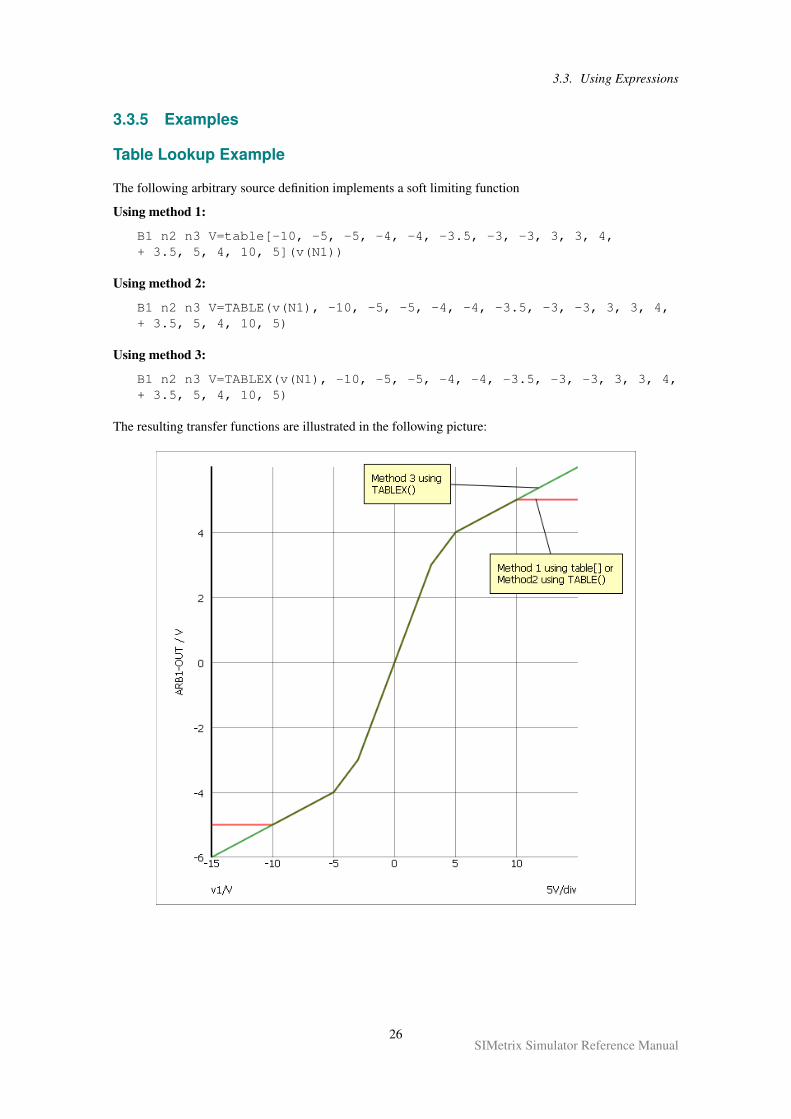
3.3. Using Expressions
3.3.5 Examples
Table Lookup Example
The following arbitrary source definition implements a soft limiting function
Using method 1:
B1 n2 n3 V=table[-10, -5, -5, -4, -4, -3.5, -3, -3, 3, 3, 4,+ 3.5, 5, 4, 10, 5](v(N1))
Using method 2:
B1 n2 n3 V=TABLE(v(N1), -10, -5, -5, -4, -4, -3.5, -3, -3, 3, 3, 4,+ 3.5, 5, 4, 10, 5)
Using method 3:
B1 n2 n3 V=TABLEX(v(N1), -10, -5, -5, -4, -4, -3.5, -3, -3, 3, 3, 4,+ 3.5, 5, 4, 10, 5)
The resulting transfer functions are illustrated in the following picture:
26SIMetrix Simulator Reference Manual
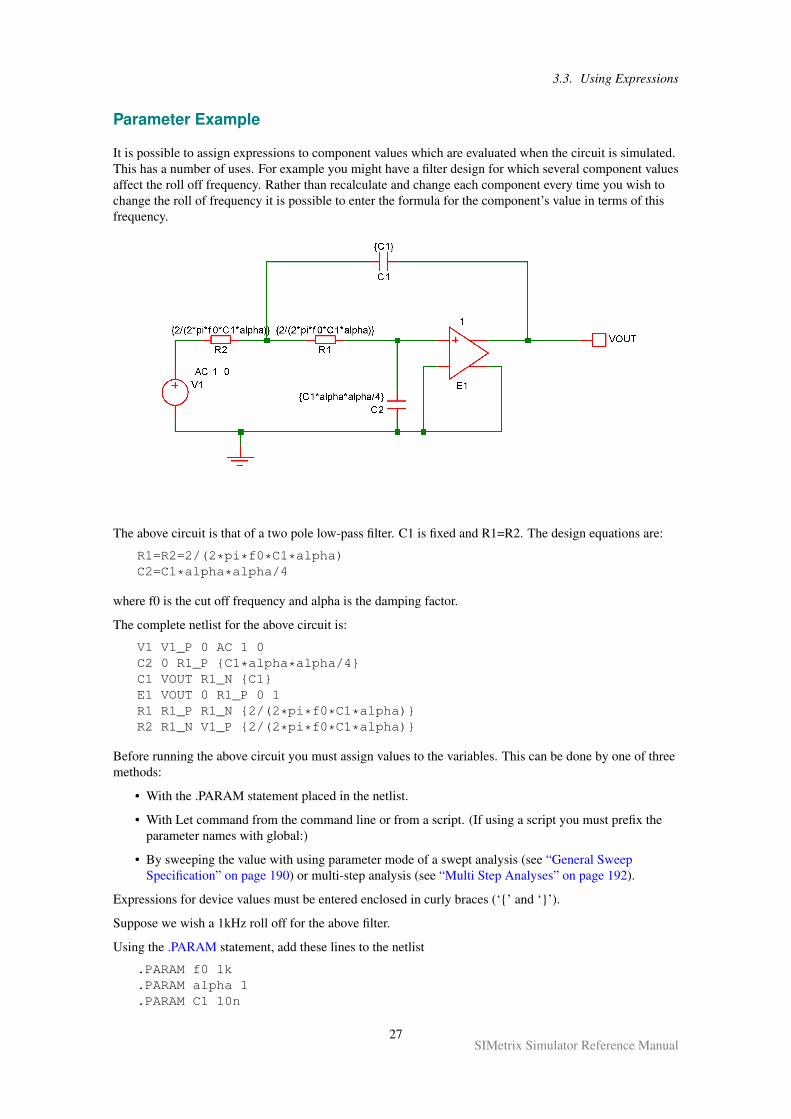
3.3. Using Expressions
Parameter Example
It is possible to assign expressions to component values which are evaluated when the circuit is simulated.This has a number of uses. For example you might have a filter design for which several component valuesaffect the roll off frequency. Rather than recalculate and change each component every time you wish tochange the roll of frequency it is possible to enter the formula for the component’s value in terms of thisfrequency.
The above circuit is that of a two pole low-pass filter. C1 is fixed and R1=R2. The design equations are:
R1=R2=2/(2*pi*f0*C1*alpha)C2=C1*alpha*alpha/4
where f0 is the cut off frequency and alpha is the damping factor.
The complete netlist for the above circuit is:
V1 V1_P 0 AC 1 0C2 0 R1_P C1*alpha*alpha/4C1 VOUT R1_N C1E1 VOUT 0 R1_P 0 1R1 R1_P R1_N 2/(2*pi*f0*C1*alpha)R2 R1_N V1_P 2/(2*pi*f0*C1*alpha)
Before running the above circuit you must assign values to the variables. This can be done by one of threemethods:
• With the .PARAM statement placed in the netlist.
• With Let command from the command line or from a script. (If using a script you must prefix theparameter names with global:)
• By sweeping the value with using parameter mode of a swept analysis (see “General SweepSpecification” on page 190) or multi-step analysis (see “Multi Step Analyses” on page 192).
Expressions for device values must be entered enclosed in curly braces (‘’ and ‘’).
Suppose we wish a 1kHz roll off for the above filter.
Using the .PARAM statement, add these lines to the netlist
.PARAM f0 1k
.PARAM alpha 1
.PARAM C1 10n
27SIMetrix Simulator Reference Manual
3.3. Using Expressions
Using the Let command, you would type:
Let f0=1kLet alpha=1Let C1=10n
If you then wanted to alter the damping factor to 0.8 you only need to type in its new value:
Let alpha=0.8
then re-run the simulator.
To execute the Let commands from within a script, prefix the parameter names with global:. E.g. “Letglobal:f0=1k”
In many cases the .PARAM approach is more convenient as the values can be stored with the schematic.
3.3.6 Optimisation
Overview
An optimisation algorithm may be enabled for expressions used to define arbitrary sources and anyexpression containing a swept parameter. This can improve performance if a large number of suchexpressions are present in a design.
The optimiser dramatically improves the simulation performance of the power device models developedby Infineon. See “Optimiser Performance” on page 28.
Why is it Needed?
The simulator’s core algorithms use the Newton-Raphson iteration method to solve non-linear equations.This method requires the differential of each equation to be calculated and for arbitrary sources, thisdifferentiation is performed symbolically. So as well as calculating the user supplied expression, thesimulator must also evaluate the expression’s differential with respect to each dependent variable. Thesedifferential expressions nearly always have some sub-expressions in common with sub-expressions in themain equation and other differentials. Calculation speed can be improved by arranging to evaluate thesesub-expressions only once. This is the main task performed by the optimiser. However, it also eliminatesfactors found on both the numerator and denominator of an expression as well as collecting constantstogether wherever possible.
Using the Optimiser
The optimiser is automatically enabled and no action is required to make use of it. If desired, it can bedisabled using:
.OPTIONS optimise=0
Optimiser Performance
The optimisation algorithm was added to SIMetrix primarily to improve the performance of some publiclyavailable power device models from Infineon. These models make extensive use of arbitrary sources andmany expressions are defined using .FUNC.
The performance improvement gained for these model is in some cases dramatic. For example a simpleswitching PSU circuit using a SGP02N60 IGBT ran around 5 times faster with the optimiser enabled andthere are other devices that show an even bigger improvement.
28SIMetrix Simulator Reference Manual
3.4. Subcircuits
Accuracy
The optimiser simply changes the efficiency of evaluation and doesn’t change the calculation beingperformed in any way. However, performing a calculation in a different order can alter the least significantdigits in the final result. In some simulations, these tiny changes can result in much larger changes incircuit solution. So, you may find that switching the optimiser on and off may change the results slightly.
3.4 Subcircuits
3.4.1 Overview
Subcircuits are a method of defining a circuit block which can be referenced any number of times by asingle netlist line or schematic device. Subcircuits are the method used to define many device models suchas op-amps.
3.4.2 Subcircuit Definition
Subcircuits begin with the .SUBCKT statement and end with .ENDS. A subcircuit definition is of the form:
.SUBCKT subcircuit_name nodelist [[params:] default_parameter_list]definition_lines.ENDS
subcircuit_name Name of the subcircuit and is used to reference it in the mainnetlist.
nodelist Any number of node names and are used for external connections. Thesubcircuit call (using an ‘X’ device) would use a matching number ofnodes in the same order.
default_parameter_list List of parameters and their default values in the form name=value.Subcircuit parameters are explained in “Using Expressions” onpage 17.
definition_lines List of valid device and model lines. In addition, .NODESET, .IC and.KEEP lines may also be placed in a subcircuit.
Example
This is an example of an opamp subcircuit called SXOA1000. VINP, VINN VOUT VCC and VEE are itsexternal connections. The three .model lines define devices that are local, that is, they are only accessiblewithin the subcircuit definition.
.subckt SXOA1000 VINP VINN VOUT VCC VEEI2 D2_N VEE 100uI1 Q3_E VEE 100uC1 VOUT R1_P 10pD1 Q7_C D1_N D1D2 D1_N D2_N D1D3 VEE Q3_E D1Q2 VEE D2_N VOUT 0 P1Q3 Q3_C R3_P Q3_E 0 N1Q1 VCC Q7_C VOUT 0 N1Q6 Q3_C Q3_C VCC 0 P1
29SIMetrix Simulator Reference Manual
3.4. Subcircuits
Q7 Q7_C Q5_C VCC 0 P1R1 R1_P Q5_C 100Q4 Q5_C R2_N Q3_E 0 N1R2 VINP R2_N 1KQ5 Q5_C Q3_C VCC 0 P1R3 R3_P VINN 1K
.model N1 NPN VA=100 TF=1e-9
.model P1 PNP VA=100 TF=1e-9
.model D1 D
.ends
Where to Place Subcircuit Definition
Subcircuit definitions may be placed in a number of locations.
• Directly in the netlist. This is the best place if the subcircuit is specific to a particular design. If youare entering the circuit using the schematic editor, see “Simulator Reference Manual/Running theSimulator/Using the Simulator with the SIMetrix Schematic Editor/Adding Extra Netlist Lines” onpage 2 to find out how to add additional lines to the netlist.
• Put in a separate file and pull in to the schematic with .INC statement placed in the netlist.
• Put in a library file and reference in schematic with SIMetrix form of “.LIB” on page 210 statementplaced in the netlist. Similar to 2. but more efficient if library has many models not used in theschematic. Only the devices required will be read in.
• Put in a library file and install as a model library. See User’s Manual/Device Library and PartsManagement/Installing Models for full details.
3.4.3 Subcircuit Instance
Once a subcircuit has been defined, any number of instances of it may be created. These are of the form:
Xxxxx nodelist sub_circuitname [ [params:|:] parameters]
nodelist List of nodes, each of which will connect to its corresponding node in thesubcircuit’s definition. The number of nodes in the instance must exactlymatch the number of nodes in the definition.
sub_circuitname Name of the subcircuit definition.
parameters List of parameter names and their values in the form name=value. Thesemay be referenced in the subcircuit definition. Subcircuit parameters areexplained below.
3.4.4 Passing Parameters to Subcircuits
You can pass parameters to a subcircuit. Consider the filter example provided in “Using Expressions” onpage 17. Supposing we wanted to define several filters with different characteristics. We could use asubcircuit to define the filter but the values of the components in the filter need to be different for eachinstance. This can be achieved by passing the parameter values to each instance of the subcircuit.
So:
** Definition
30SIMetrix Simulator Reference Manual
3.4. Subcircuits
.SUBCKT Filter IN OUT params: C1=1n alpha=1 f0=1kC2 0 R1_P C1*alpha*alpha/4C1 OUT R1_N C1E1 OUT 0 R1_P 0 1R1 R1_P R1_N 2/(2*pi*f0*C1*alpha)R2 R1_N IN 2/(2*pi*f0*C1*alpha).ENDS
** Subcircuit instanceX1 V1_P VOUT Filter : C1=10n alpha=1 f0=10k
** AC sourceV1 V1_P 0 AC 1 0
In the above example the parameters after params: in the .subckt line define default values should anyparameters be omitted from the subcircuit instance line. It is not compulsory to define defaults but isgenerally recommended.
Note
In the syntax definition for both subcircuit definitions and subcircuit instances, the params: specifier isshown as optional. If params: is included the ‘=’ separating the parameter names and their values becomesoptional.
3.4.5 Nesting Subcircuits
Subcircuit definitions may contain both calls to other subcircuits and local subcircuit definitions.
If a subcircuit definition is placed within another subcircuit definition, it becomes local. That is, it is onlyavailable to its host subcircuit.
Calls to subcircuits may not be recursive. A subcircuit may not directly or indirectly call its own definition.
3.4.6 Global Nodes
Sometimes it is desirable to refer to a node at the circuit’s top level from within a subcircuit without havingto explicitly pass it. This is sometimes useful for supply rails.
SIMetrix provides three methods.
• ‘#’ prefix. Any node within a subcircuit prefixed with ‘#’ will connect to a top level node of thesame name without the ‘#’ prefix.
• ‘$g_’ prefix. Any node in the circuit prefixed ‘$g_’ will be treated as global.
• Using .GLOBAL.
The second approach is compatible with PSpice®. The third approach is compatible with Hspice®
Note the first two approaches are subtly different. In the second approach the ‘$g_’ prefix must be appliedto all connected nodes, whereas in the first approach the ‘#’ prefix must be applied only to subcircuit nodes.
3.4.7 Subcircuit Preprocessing
SIMetrix features a netlist preprocessor that is usually used for SIMPLIS simulations and was developedfor that purpose. The preprocessor has some features that aren’t available in the native simulator and forthis reason it would be useful to be able to use the preprocessor for SIMetrix simulations.
31SIMetrix Simulator Reference Manual
3.5. Model Binning
It is not necessary to apply the preprocessor to the entire netlist. Any subcircuit call that definespreprocessor variables using the ‘vars:’ specifier will be passed to the preprocessor. For example:
X$C1 R1_P 0 ELEC_CAP_L13 vars: LEVEL=3 CC=1m+ RSH_CC=1Meg IC=0 RESR=10m LESL=100n USEIC=1
calls the ELEC_CAP_L13 subcircuit but passes it through the preprocessor first. This model is a model foran electrolytic capacitor and uses a number of .IF statements to select model features according to theLEVEL parameter.
The preprocessor also provides a means of generating multiple devices using .WHILE. For information onthe preprocessor, see the SIMPLIS Reference Manual/Running SIMPLIS/Netlist Preprocessor.
3.5 Model Binning
3.5.1 Overview
Some devices can be binned. This means that a number of different model definitions can be provided forthe same device with each being valid over a limited range of some device parameter or parameters. Thesimulator will automatically select the appropriate model according to the value given for the deviceparameters.
Currently only BSIM3, BSIM4 and HiSIM HV MOSFETs may be binned. The binning is controlled bythe length and width device parameters (L and W) while the LMIN, LMAX, WMIN and WMAX modelparameters specify the valid range for each model.
Important Note
The binned models should be placed directly in the netlist or called using either .INC or the Hspice® formof .LIB. They will not work correctly when installed as a model library or accessed with the SIMetrix formof .LIB.
3.5.2 Defining Binned Models
Binned models are defined as a set consisting of two or more .MODEL definitions. Each of the definitionsmust be named using the following format:
root_name.id
root_name Name used by the device to call the model. Must be the same for all modeldefinitions in a set
id Arbitrary name that must be unique for each model in a set. This wouldusually be a number but this is not a requirement
Each model definition must also contain a MIN/MAX parameter pair for each bin control parameter. Forthe BSIM3 MOSFET there are two bin control parameters, namely L and W with correspondingMIN/MAX pairs LMIN/LMAX and WMIN/WMAX. For a binned BSIM3 model, all four must bepresent. These parameters define the range of L and W over which the model is valid. When a model isrequired, the simulator searches all models with the same root_name for a definition whose LMIN/LMAXand WMIN/WMAX parameters are compatible with the device’s L and W.
3.5.3 Example
32SIMetrix Simulator Reference Manual
3.6. Language Differences
.MODEL N1.1 NMOS LEVEL=49 ... parameters ...+ LMIN=1u LMAX=4u WMIN=1u WMAX=4u
.MODEL N1.2 NMOS LEVEL=49 ... parameters ...+ LMIN=4u LMAX=10u WMIN=1u WMAX=4u
.MODEL N1.3 NMOS LEVEL=49 ... parameters ...+ LMIN=1u LMAX=4u WMIN=4u WMAX=10u
.MODEL N1.4 NMOS LEVEL=49 ... parameters ...+ LMIN=4u LMAX=10u WMIN=4u WMAX=10u
** This device will use N1.1M1 1 2 3 4 N1 L=2u W=2u
** This device will use N1.2M2 1 2 3 4 N1 L=6u W=2u
** This device will use N1.3M3 1 2 3 4 L=2u W=7u
** This device will use N1.4M4 1 2 3 4 L=6u W=7u
3.6 Language Differences
SIMetrix is compatible with some PSpice® and Hspice® extensions mainly so that it can read externalmodel files. Some aspects of these alternative formats are incompatible with the SIMetrix native formatand in such cases it is necessary to declare the language being used. See “Language Declaration” onpage 9 for details on how to do this.
The following sections describe the incompatibilities between the three languages.
3.6.1 Inline Comment
Hspice® uses the dollar (‘$’) symbol for inline comments while SIMetrix and PSpice® use a semi-colon(‘;’). The language declaration described above determines what character is used.
3.6.2 Unlabelled Device Parameters
The problem with unlabelled device parameters is illustrated with the following examples.
The following lines are legal in Hspice® mode but illegal in SIMetrix mode.
.PARAM area=2Q1 C B E S N1 area
Q1 will have an area of 2. Conversely the following is legal in SIMetrix but is illegal in Hspice®:
.PARAM area=2Q1 C B E S N1 area area
Again Q1 has an area of 2.
The problem is that SIMetrix does not require ‘=’ to separate parameter names with their values whereasHspice® does. area is a legal BJT parameter name so in the first example SIMetrix can’t tell whether area
33SIMetrix Simulator Reference Manual
3.7. Customising Device Configuration
refers to the name of the BJT parameter or the name of the .PARAM parameter defined in the previousline. Hspice® can tell the difference because if area meant the BJT parameter name it would be followedby an ‘=’.
This line is legal and will be correctly interpreted in both modes
.PARAM area=2Q1 C B E S N1 area=area
Although Hspice® always requires the ‘=’ to separate parameter names and values, it continues to beoptional in SIMetrix even in Hspice® mode. It only becomes compulsory where an ambiguity needs to beresolved as in the second example above.
3.6.3 LOG() and PWR()
The LOG() function means log to the base 10 in SIMetrix but in PSpice® and Hspice® means log to thebase e. PWR() in PSpice® and SIMetrix means |x|y whereas in Hspice® it means “if x ≥ 0, |x|y else−|x|y”. The language declaration only affects the definition when used in expressions to define model anddevice parameters. When used in arbitrary source expressions, the language assumed is controlled by themethod of implementing the device as follows:
SIMetrix:
B1 1 2 V=expression
PSpice®
E1 1 2 VALUE = expression
Hspice®
E1 1 2 VOL = `expression'
Note that the function LN() always means log to base e and LOG10() always means log to base 10. Werecommend that these functions are always used in preference to LOG to avoid confusion.
3.7 Customising Device Configuration
3.7.1 Overview
Models for discrete devices and for integrated circuit processes come from a variety of sources and areoften designed for particular simulators, in particular, PSpice and Hspice. These simulators are notgenerally compatible with each other so it is not easy for SIMetrix to be simultaneously compatible withboth. Further, SIMetrix itself needs to retain backward compatibility with its own earlier versions.
An example of conflict can be found with the standard diode. The SIMetrix diode with no level parameterspecified is mainly compatible with PSpice. But the standard Hspice diode is quite different and notcompatible. The SIMetrix Level=3 diode is however compatible with Hspice both for level=1 and level=3.To use Hspice level=1 diode models the user has to edit the model so that level is changed to 3.
It is not always convenient to modify model files and for this reason SIMetrix provides two methods toglobally change level numbers and model names needed to select a particular device model. These are:
“.MAP statement” on page 211
“Device configuration file” on page 212
Both methods work the same way; the difference is the scope and lifetime of the changes. .MAP worksonly for the netlist in which it appears, whereas the device configuration file is a permanent setting andworks for all simulations.
34SIMetrix Simulator Reference Manual
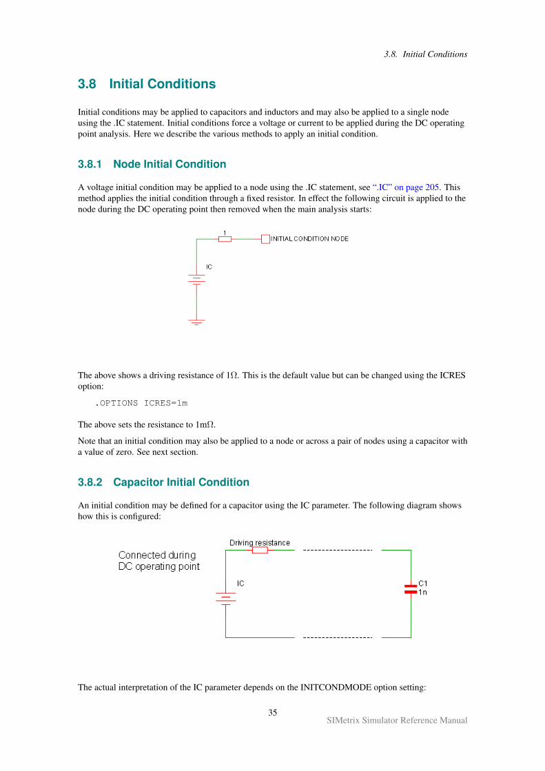
3.8. Initial Conditions
3.8 Initial Conditions
Initial conditions may be applied to capacitors and inductors and may also be applied to a single nodeusing the .IC statement. Initial conditions force a voltage or current to be applied during the DC operatingpoint analysis. Here we describe the various methods to apply an initial condition.
3.8.1 Node Initial Condition
A voltage initial condition may be applied to a node using the .IC statement, see “.IC” on page 205. Thismethod applies the initial condition through a fixed resistor. In effect the following circuit is applied to thenode during the DC operating point then removed when the main analysis starts:
The above shows a driving resistance of 1Ω. This is the default value but can be changed using the ICRESoption:
.OPTIONS ICRES=1m
The above sets the resistance to 1mΩ.
Note that an initial condition may also be applied to a node or across a pair of nodes using a capacitor witha value of zero. See next section.
3.8.2 Capacitor Initial Condition
An initial condition may be defined for a capacitor using the IC parameter. The following diagram showshow this is configured:
The actual interpretation of the IC parameter depends on the INITCONDMODE option setting:
35SIMetrix Simulator Reference Manual
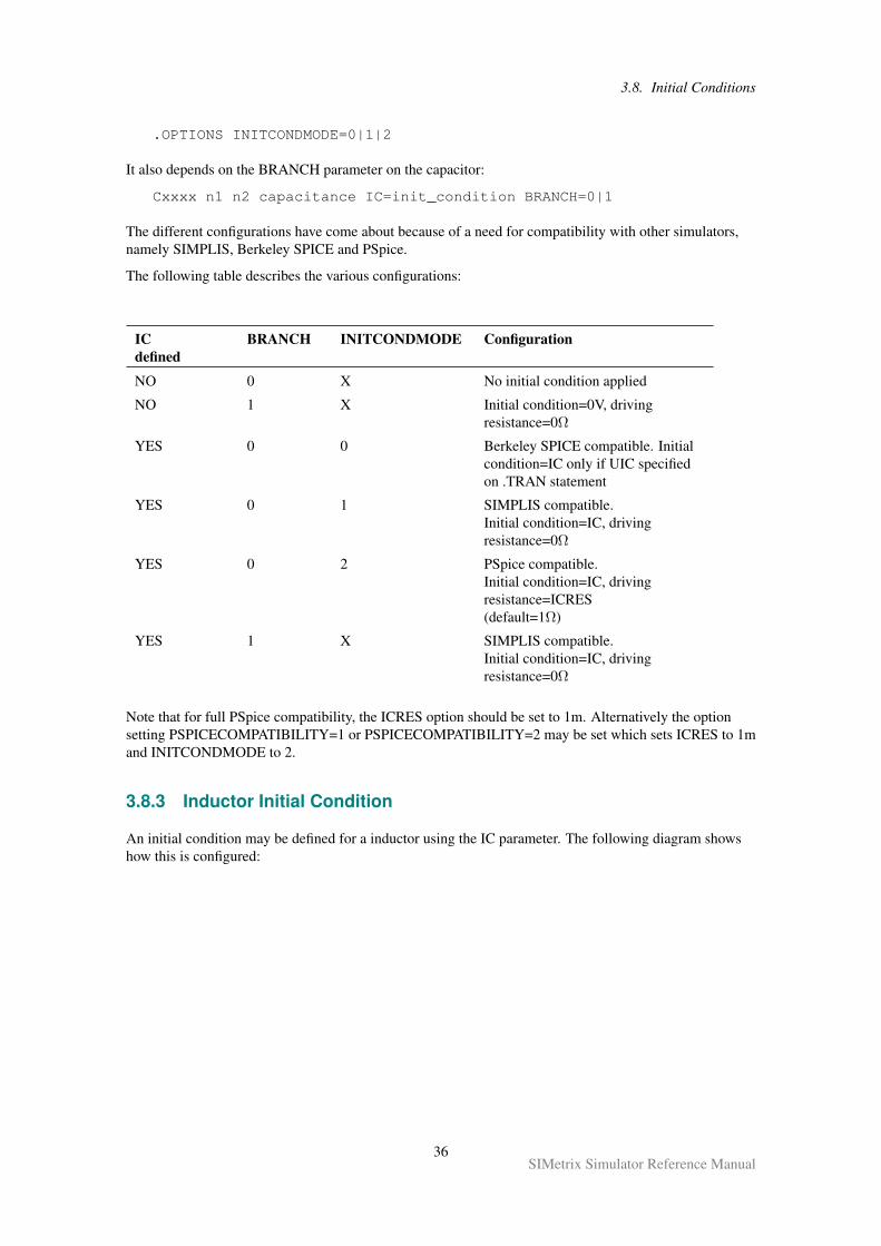
3.8. Initial Conditions
.OPTIONS INITCONDMODE=0|1|2
It also depends on the BRANCH parameter on the capacitor:
Cxxxx n1 n2 capacitance IC=init_condition BRANCH=0|1
The different configurations have come about because of a need for compatibility with other simulators,namely SIMPLIS, Berkeley SPICE and PSpice.
The following table describes the various configurations:
ICdefined
BRANCH INITCONDMODE Configuration
NO 0 X No initial condition applied
NO 1 X Initial condition=0V, drivingresistance=0Ω
YES 0 0 Berkeley SPICE compatible. Initialcondition=IC only if UIC specifiedon .TRAN statement
YES 0 1 SIMPLIS compatible.Initial condition=IC, drivingresistance=0Ω
YES 0 2 PSpice compatible.Initial condition=IC, drivingresistance=ICRES(default=1Ω)
YES 1 X SIMPLIS compatible.Initial condition=IC, drivingresistance=0Ω
Note that for full PSpice compatibility, the ICRES option should be set to 1m. Alternatively the optionsetting PSPICECOMPATIBILITY=1 or PSPICECOMPATIBILITY=2 may be set which sets ICRES to 1mand INITCONDMODE to 2.
3.8.3 Inductor Initial Condition
An initial condition may be defined for a inductor using the IC parameter. The following diagram showshow this is configured:
36SIMetrix Simulator Reference Manual
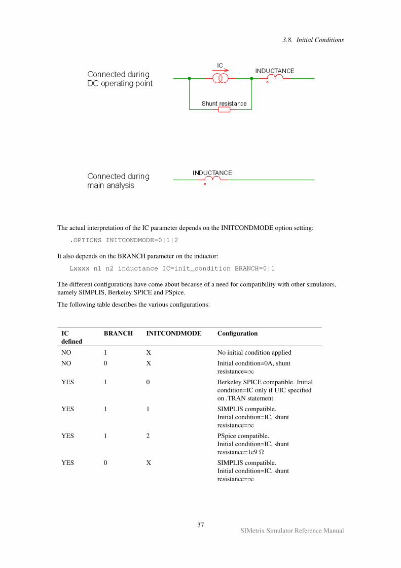
3.8. Initial Conditions
The actual interpretation of the IC parameter depends on the INITCONDMODE option setting:
.OPTIONS INITCONDMODE=0|1|2
It also depends on the BRANCH parameter on the inductor:
Lxxxx n1 n2 inductance IC=init_condition BRANCH=0|1
The different configurations have come about because of a need for compatibility with other simulators,namely SIMPLIS, Berkeley SPICE and PSpice.
The following table describes the various configurations:
ICdefined
BRANCH INITCONDMODE Configuration
NO 1 X No initial condition applied
NO 0 X Initial condition=0A, shuntresistance=∞
YES 1 0 Berkeley SPICE compatible. Initialcondition=IC only if UIC specifiedon .TRAN statement
YES 1 1 SIMPLIS compatible.Initial condition=IC, shuntresistance=∞
YES 1 2 PSpice compatible.Initial condition=IC, shuntresistance=1e9 Ω
YES 0 X SIMPLIS compatible.Initial condition=IC, shuntresistance=∞
37SIMetrix Simulator Reference Manual
4.3. AC Table Lookup
Chapter 4
Analog Device Reference
4.1 Overview
This chapter provides the full details of every option and parameter available with every primitive analogdevice that the simulator supports.
For documentation on digital and mixed signal devices supplied with SIMetrix, please see “Digital/Mixedsignal Device Reference” on page 134.
4.2 Further Documentation
Some devices are fully documented by their developers and we have not repeated that documentation here.In all cases the documents may be found on the installation CDROM. We no longer ship a physicalCDROM but its contents may be browsed and an image downloaded from our web site. Visit:
http://www.simetrix.co.uk/app/product-installation.htm
then click on Download links. You will need a user name and password to access this page. An automatedsystem is available to obtain this and you will find details at the above link.
4.3 AC Table Lookup (including S-Parameters)
4.3.1 Netlist Entry
Uxxx node_pairs modelname
Where
node_pairs Pairs of nodes for each port. So for example, a two port device has fournodes.
modelname Model name
4.3.2 Model Format
.MODEL modelname actable LOAD=filename [NUMPORTS=number_of_ports ] [ DCMETHOD=extrapolate|extend ] [
38SIMetrix Simulator Reference Manual
4.4. Arbitrary Source
DCPARAMS=[dcgainvalues] ]
Where:
filename Name of file containing frequency table. File uses Touchstone format andmay contain s-parameters or y-parameters. Other parameter types are notcurrently supported.
number_of_ports Number of ports. Default value is 2. If y-parameters are supplied, anynumber of ports may be specified. If s-parameters are specified, thenumber of ports must be 1 or 2.
DCMETHOD Has values of ‘extrapolate’ or ‘extend’. This determines how the DC gainsare calculated if they are not explicitly defined using the DCPARAMSparameter or with an explicit F=0 term in the definition file. With‘extrapolate’, the dc values are calculated by extrapolating back to zero;with ‘extend’, the DC gain is the same as the lowest frequencygain.
dcgainvalues Vector providing the DC gain values for the network. This is expected tobe an n x n matrix where n is the number of ports.
4.3.3 AC Table Notes
The AC Table device implements a circuit device that is defined by a frequency lookup table. This deviceoperates only in the small signal analysis modes, AC, Noise and TF. In transient and DC analyses itbehaves like a simple linear DC gain block with no frequency dependence.
The lookup table for this device must be defined by a file and uses the industry standard ‘Touchstone’format. The full details of this format are supplied as a separate document and maybe found on theSIMetrix install CDROM and at our web site. Please visit “Further Documentation” on page 38 for details.The document is freely distributable under the terms described therein and may also be found at variousInternet sites.
The SIMetrix implementation of the touchstone format includes the following:
1. Y-parameters to any number of ports
2. 1 and 2 port s-parameters
Z, H and G parameters are not supported. Also, noise parameters are not supported.
Touchstone files traditionally use the extension snp where n indicates the number of ports. Be aware thatSIMetrix uses the NUMPORTS parameter in the .model statement to determine the number of ports andwill ignore the value of n in the filename extension.
4.4 Arbitrary Source
4.4.1 Netlist Entry
Voltage source:
Bxxxx n+ n- [MIN=min_value] [MAX=max_value] V=expression
Current source:
Bxxxx n+ n- [MIN=min_value] [MAX=max_value] [M=multiplier] I=expression
Charge source:
39SIMetrix Simulator Reference Manual
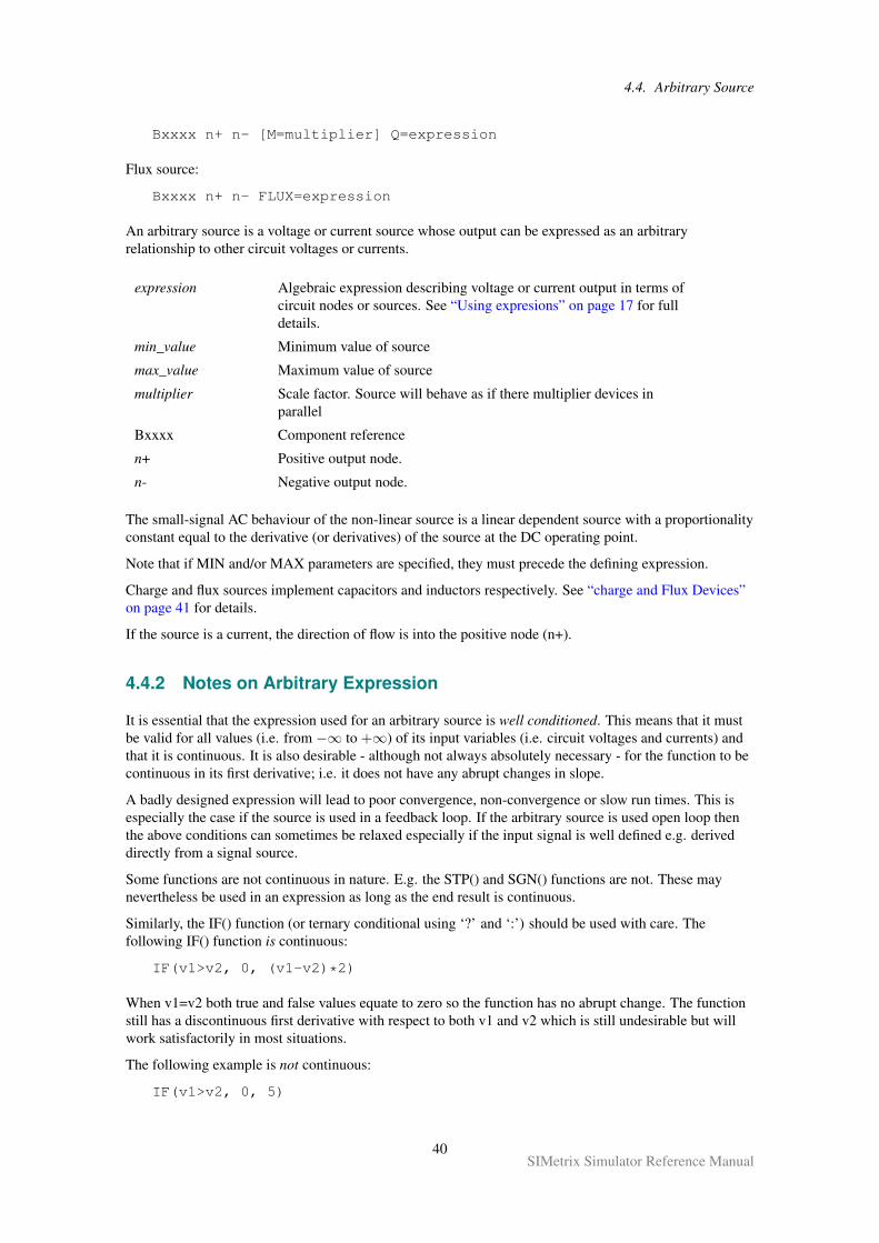
4.4. Arbitrary Source
Bxxxx n+ n- [M=multiplier] Q=expression
Flux source:
Bxxxx n+ n- FLUX=expression
An arbitrary source is a voltage or current source whose output can be expressed as an arbitraryrelationship to other circuit voltages or currents.
expression Algebraic expression describing voltage or current output in terms ofcircuit nodes or sources. See “Using expresions” on page 17 for fulldetails.
min_value Minimum value of source
max_value Maximum value of source
multiplier Scale factor. Source will behave as if there multiplier devices inparallel
Bxxxx Component reference
n+ Positive output node.
n- Negative output node.
The small-signal AC behaviour of the non-linear source is a linear dependent source with a proportionalityconstant equal to the derivative (or derivatives) of the source at the DC operating point.
Note that if MIN and/or MAX parameters are specified, they must precede the defining expression.
Charge and flux sources implement capacitors and inductors respectively. See “charge and Flux Devices”on page 41 for details.
If the source is a current, the direction of flow is into the positive node (n+).
4.4.2 Notes on Arbitrary Expression
It is essential that the expression used for an arbitrary source is well conditioned. This means that it mustbe valid for all values (i.e. from −∞ to +∞) of its input variables (i.e. circuit voltages and currents) andthat it is continuous. It is also desirable - although not always absolutely necessary - for the function to becontinuous in its first derivative; i.e. it does not have any abrupt changes in slope.
A badly designed expression will lead to poor convergence, non-convergence or slow run times. This isespecially the case if the source is used in a feedback loop. If the arbitrary source is used open loop thenthe above conditions can sometimes be relaxed especially if the input signal is well defined e.g. deriveddirectly from a signal source.
Some functions are not continuous in nature. E.g. the STP() and SGN() functions are not. These maynevertheless be used in an expression as long as the end result is continuous.
Similarly, the IF() function (or ternary conditional using ‘?’ and ‘:’) should be used with care. Thefollowing IF() function is continuous:
IF(v1>v2, 0, (v1-v2)*2)
When v1=v2 both true and false values equate to zero so the function has no abrupt change. The functionstill has a discontinuous first derivative with respect to both v1 and v2 which is still undesirable but willwork satisfactorily in most situations.
The following example is not continuous:
IF(v1>v2, 0, 5)
40SIMetrix Simulator Reference Manual
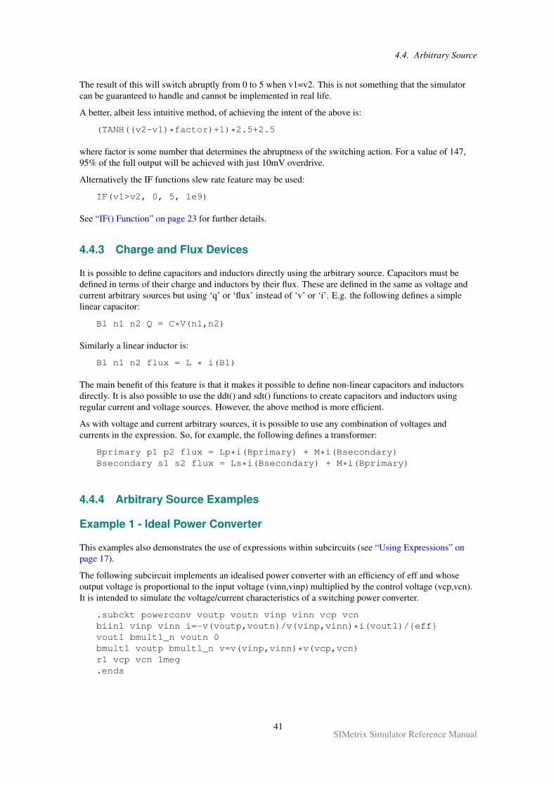
4.4. Arbitrary Source
The result of this will switch abruptly from 0 to 5 when v1=v2. This is not something that the simulatorcan be guaranteed to handle and cannot be implemented in real life.
A better, albeit less intuitive method, of achieving the intent of the above is:
(TANH((v2-v1)*factor)+1)*2.5+2.5
where factor is some number that determines the abruptness of the switching action. For a value of 147,95% of the full output will be achieved with just 10mV overdrive.
Alternatively the IF functions slew rate feature may be used:
IF(v1>v2, 0, 5, 1e9)
See “IF() Function” on page 23 for further details.
4.4.3 Charge and Flux Devices
It is possible to define capacitors and inductors directly using the arbitrary source. Capacitors must bedefined in terms of their charge and inductors by their flux. These are defined in the same as voltage andcurrent arbitrary sources but using ‘q’ or ‘flux’ instead of ‘v’ or ‘i’. E.g. the following defines a simplelinear capacitor:
B1 n1 n2 Q = C*V(n1,n2)
Similarly a linear inductor is:
B1 n1 n2 flux = L * i(B1)
The main benefit of this feature is that it makes it possible to define non-linear capacitors and inductorsdirectly. It is also possible to use the ddt() and sdt() functions to create capacitors and inductors usingregular current and voltage sources. However, the above method is more efficient.
As with voltage and current arbitrary sources, it is possible to use any combination of voltages andcurrents in the expression. So, for example, the following defines a transformer:
Bprimary p1 p2 flux = Lp*i(Bprimary) + M*i(Bsecondary)Bsecondary s1 s2 flux = Ls*i(Bsecondary) + M*i(Bprimary)
4.4.4 Arbitrary Source Examples
Example 1 - Ideal Power Converter
This examples also demonstrates the use of expressions within subcircuits (see “Using Expressions” onpage 17).
The following subcircuit implements an idealised power converter with an efficiency of eff and whoseoutput voltage is proportional to the input voltage (vinn,vinp) multiplied by the control voltage (vcp,vcn).It is intended to simulate the voltage/current characteristics of a switching power converter.
.subckt powerconv voutp voutn vinp vinn vcp vcnbiin1 vinp vinn i=-v(voutp,voutn)/v(vinp,vinn)*i(vout1)/effvout1 bmult1_n voutn 0bmult1 voutp bmult1_n v=v(vinp,vinn)*v(vcp,vcn)r1 vcp vcn 1meg.ends
41SIMetrix Simulator Reference Manual
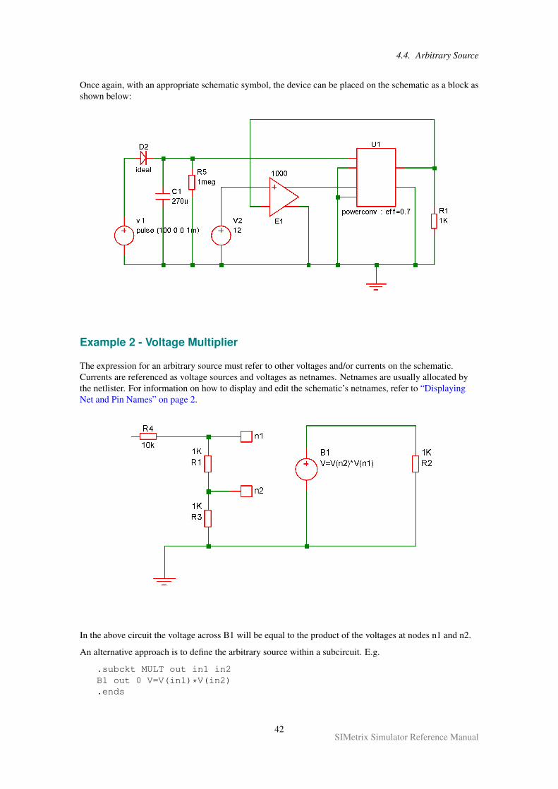
4.4. Arbitrary Source
Once again, with an appropriate schematic symbol, the device can be placed on the schematic as a block asshown below:
Example 2 - Voltage Multiplier
The expression for an arbitrary source must refer to other voltages and/or currents on the schematic.Currents are referenced as voltage sources and voltages as netnames. Netnames are usually allocated bythe netlister. For information on how to display and edit the schematic’s netnames, refer to “DisplayingNet and Pin Names” on page 2.
In the above circuit the voltage across B1 will be equal to the product of the voltages at nodes n1 and n2.
An alternative approach is to define the arbitrary source within a subcircuit. E.g.
.subckt MULT out in1 in2B1 out 0 V=V(in1)*V(in2).ends
42SIMetrix Simulator Reference Manual
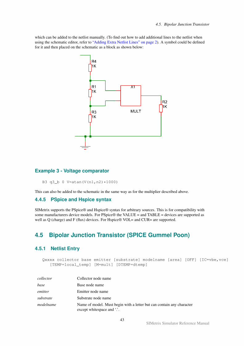
4.5. Bipolar Junction Transistor
which can be added to the netlist manually. (To find out how to add additional lines to the netlist whenusing the schematic editor, refer to “Adding Extra Netlist Lines” on page 2). A symbol could be definedfor it and then placed on the schematic as a block as shown below:
Example 3 - Voltage comparator
B3 q3_b 0 V=atan(V(n1,n2)*1000)
This can also be added to the schematic in the same way as for the multiplier described above.
4.4.5 PSpice and Hspice syntax
SIMetrix supports the PSpice® and Hspice® syntax for arbitrary sources. This is for compatibility withsome manufacturers device models. For PSpice® the VALUE = and TABLE = devices are supported aswell as Q (charge) and F (flux) devices. For Hspice® VOL= and CUR= are supported.
4.5 Bipolar Junction Transistor (SPICE Gummel Poon)
4.5.1 Netlist Entry
Qxxxx collector base emitter [substrate] modelname [area] [OFF] [IC=vbe,vce][TEMP=local_temp] [M=mult] [DTEMP=dtemp]
collector Collector node name
base Base node name
emitter Emitter node name
substrate Substrate node name
modelname Name of model. Must begin with a letter but can contain any characterexcept whitespace and ‘.’.
43SIMetrix Simulator Reference Manual
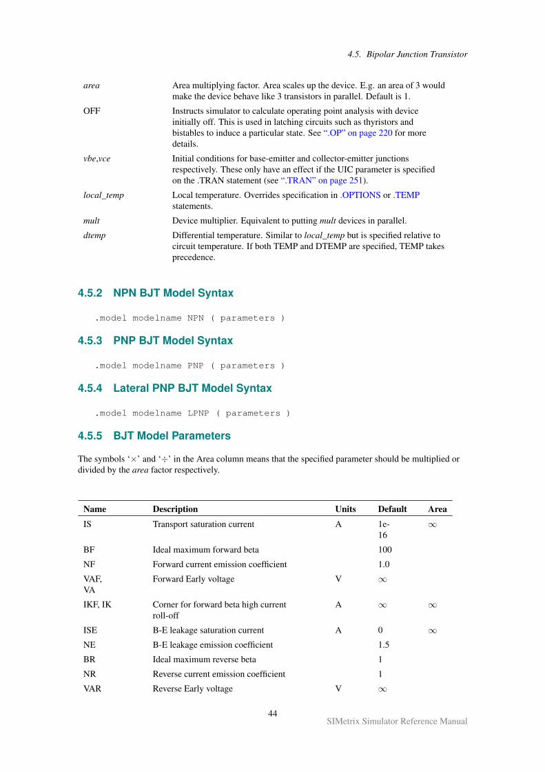
4.5. Bipolar Junction Transistor
area Area multiplying factor. Area scales up the device. E.g. an area of 3 wouldmake the device behave like 3 transistors in parallel. Default is 1.
OFF Instructs simulator to calculate operating point analysis with deviceinitially off. This is used in latching circuits such as thyristors andbistables to induce a particular state. See “.OP” on page 220 for moredetails.
vbe,vce Initial conditions for base-emitter and collector-emitter junctionsrespectively. These only have an effect if the UIC parameter is specifiedon the .TRAN statement (see “.TRAN” on page 251).
local_temp Local temperature. Overrides specification in .OPTIONS or .TEMPstatements.
mult Device multiplier. Equivalent to putting mult devices in parallel.
dtemp Differential temperature. Similar to local_temp but is specified relative tocircuit temperature. If both TEMP and DTEMP are specified, TEMP takesprecedence.
4.5.2 NPN BJT Model Syntax
.model modelname NPN ( parameters )
4.5.3 PNP BJT Model Syntax
.model modelname PNP ( parameters )
4.5.4 Lateral PNP BJT Model Syntax
.model modelname LPNP ( parameters )
4.5.5 BJT Model Parameters
The symbols ‘×’ and ‘÷’ in the Area column means that the specified parameter should be multiplied ordivided by the area factor respectively.
Name Description Units Default Area
IS Transport saturation current A 1e-16
∞
BF Ideal maximum forward beta 100
NF Forward current emission coefficient 1.0
VAF,VA
Forward Early voltage V ∞
IKF, IK Corner for forward beta high currentroll-off
A ∞ ∞
ISE B-E leakage saturation current A 0 ∞NE B-E leakage emission coefficient 1.5
BR Ideal maximum reverse beta 1
NR Reverse current emission coefficient 1
VAR Reverse Early voltage V ∞
44SIMetrix Simulator Reference Manual
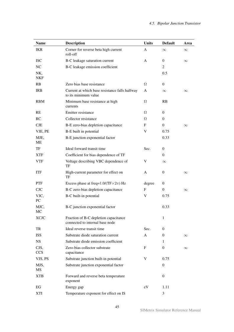
4.5. Bipolar Junction Transistor
Name Description Units Default Area
IKR Corner for reverse beta high currentroll-off
A ∞ ∞
ISC B-C leakage saturation current A 0 ∞NC B-C leakage emission coefficient 2
NK,NKF
0.5
RB Zero bias base resistance Ω 0
IRB Current at which base resistance falls halfwayto its minimum value
A ∞ ∞
RBM Minimum base resistance at highcurrents
Ω RB
RE Emitter resistance Ω 0
RC Collector resistance Ω 0
CJE B-E zero-bias depletion capacitance F 0 ∞VJE, PE B-E built in potential V 0.75
MJE,ME
B-E junction exponential factor 0.33
TF Ideal forward transit time Sec. 0
XTF Coefficient for bias dependence of TF 0
VTF Voltage describing VBC dependence ofTF
V ∞
ITF High-current parameter for effect onTF
A 0 ∞
PTF Excess phase at freq=1.0/(TF×2π) Hz degree 0
CJC B-C zero-bias depletion capacitance F 0 ∞VJC,PC
B-C built-in potential V 0.75
MJC,MC
B-C junction exponential factor 0.33
XCJC Fraction of B-C depletion capacitanceconnected to internal base node
1
TR Ideal reverse transit time Sec. 0
ISS Substrate diode saturation current A 0 ∞NS Substrate diode emission coefficient 1
CJS,CCS
Zero-bias collector substratecapacitance
F 0 ∞
VJS, PS Substrate junction built-in potential V 0.75
MJS,MS
Substrate junction exponential factor 0
XTB Forward and reverse beta temperatureexponent
0
EG Energy gap eV 1.11
XTI Temperature exponent for effect on IS 3
45SIMetrix Simulator Reference Manual
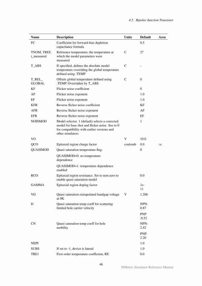
4.5. Bipolar Junction Transistor
Name Description Units Default Area
FC Coefficient for forward-bias depletioncapacitance formula
0.5
TNOM, TREF,t_measured
Reference temperature; the temperature atwhich the model parameters weremeasured
C 27
T_ABS If specified, defines the absolute modeltemperature overriding the global temperaturedefined using .TEMP
C -
T_REL_GLOBAL
Offsets global temperature defined using.TEMP. Overridden by T_ABS
C 0
KF Flicker noise coefficient 0
AF Flicker noise exponent 1.0
EF Flicker noise exponent 1.0
KFR Reverse flicker noise coefficient KF
AFR Reverse flicker noise exponent AF
EFR Reverse flicker noise exponent EF
NOISMOD Model selector. 1 (default) selects a correctedmodel for base shot and flicker noise. See to 0for compatibility with earlier versions andother simulators
1
VO V 10.0
QCO Epitaxial region charge factor coulomb 0.0 ∞QUASIMOD Quasi saturation temperature flag:
QUASIMOD=0: no temperaturedependence
QUASIMOD=1: temperature dependenceenabled
0
RCO Epitaxial region resistance. Set to non-zero toenable quasi saturation model
0.0
GAMMA Epitaxial region doping factor 1e-11
VG Quasi saturation extrapolated bandgap voltageat 0K
V 1.206
D Quasi saturation temp coeff for scatteringlimited hole carrier velocity
NPN:0.87
PNP:0.52
CN Quasi saturation temp coeff for holemobility
NPN:2.42
PNP:2.20
NEPI 1.0
SUBS If set to -1, device is lateral 1.0
TRE1 First order temperature coefficient, RE 0.0
46SIMetrix Simulator Reference Manual
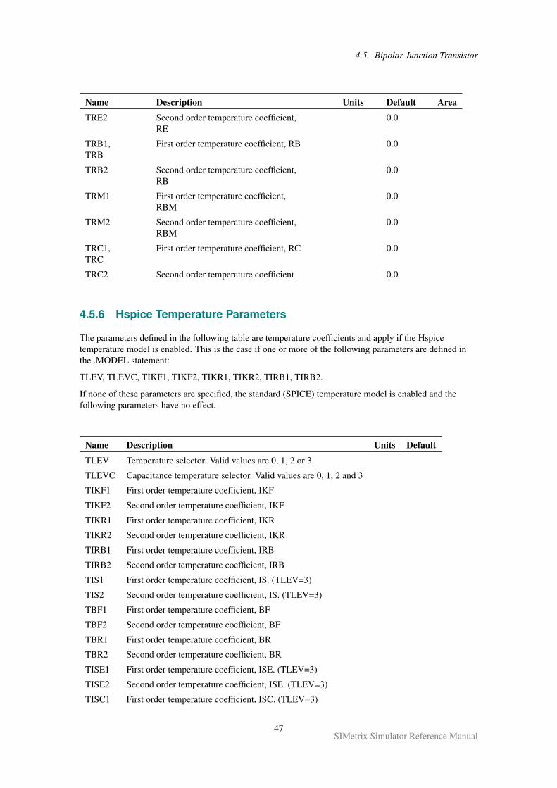
4.5. Bipolar Junction Transistor
Name Description Units Default Area
TRE2 Second order temperature coefficient,RE
0.0
TRB1,TRB
First order temperature coefficient, RB 0.0
TRB2 Second order temperature coefficient,RB
0.0
TRM1 First order temperature coefficient,RBM
0.0
TRM2 Second order temperature coefficient,RBM
0.0
TRC1,TRC
First order temperature coefficient, RC 0.0
TRC2 Second order temperature coefficient 0.0
4.5.6 Hspice Temperature Parameters
The parameters defined in the following table are temperature coefficients and apply if the Hspicetemperature model is enabled. This is the case if one or more of the following parameters are defined inthe .MODEL statement:
TLEV, TLEVC, TIKF1, TIKF2, TIKR1, TIKR2, TIRB1, TIRB2.
If none of these parameters are specified, the standard (SPICE) temperature model is enabled and thefollowing parameters have no effect.
Name Description Units Default
TLEV Temperature selector. Valid values are 0, 1, 2 or 3.
TLEVC Capacitance temperature selector. Valid values are 0, 1, 2 and 3
TIKF1 First order temperature coefficient, IKF
TIKF2 Second order temperature coefficient, IKF
TIKR1 First order temperature coefficient, IKR
TIKR2 Second order temperature coefficient, IKR
TIRB1 First order temperature coefficient, IRB
TIRB2 Second order temperature coefficient, IRB
TIS1 First order temperature coefficient, IS. (TLEV=3)
TIS2 Second order temperature coefficient, IS. (TLEV=3)
TBF1 First order temperature coefficient, BF
TBF2 Second order temperature coefficient, BF
TBR1 First order temperature coefficient, BR
TBR2 Second order temperature coefficient, BR
TISE1 First order temperature coefficient, ISE. (TLEV=3)
TISE2 Second order temperature coefficient, ISE. (TLEV=3)
TISC1 First order temperature coefficient, ISC. (TLEV=3)
47SIMetrix Simulator Reference Manual
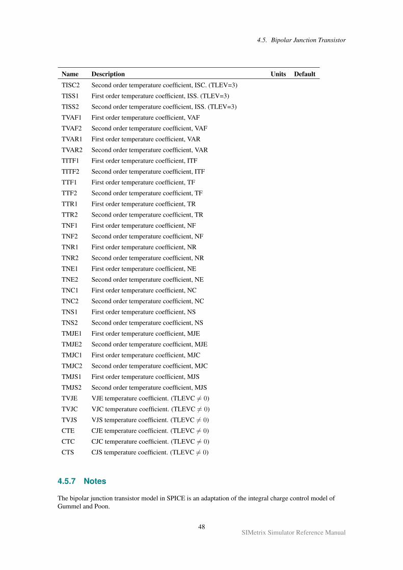
4.5. Bipolar Junction Transistor
Name Description Units Default
TISC2 Second order temperature coefficient, ISC. (TLEV=3)
TISS1 First order temperature coefficient, ISS. (TLEV=3)
TISS2 Second order temperature coefficient, ISS. (TLEV=3)
TVAF1 First order temperature coefficient, VAF
TVAF2 Second order temperature coefficient, VAF
TVAR1 First order temperature coefficient, VAR
TVAR2 Second order temperature coefficient, VAR
TITF1 First order temperature coefficient, ITF
TITF2 Second order temperature coefficient, ITF
TTF1 First order temperature coefficient, TF
TTF2 Second order temperature coefficient, TF
TTR1 First order temperature coefficient, TR
TTR2 Second order temperature coefficient, TR
TNF1 First order temperature coefficient, NF
TNF2 Second order temperature coefficient, NF
TNR1 First order temperature coefficient, NR
TNR2 Second order temperature coefficient, NR
TNE1 First order temperature coefficient, NE
TNE2 Second order temperature coefficient, NE
TNC1 First order temperature coefficient, NC
TNC2 Second order temperature coefficient, NC
TNS1 First order temperature coefficient, NS
TNS2 Second order temperature coefficient, NS
TMJE1 First order temperature coefficient, MJE
TMJE2 Second order temperature coefficient, MJE
TMJC1 First order temperature coefficient, MJC
TMJC2 Second order temperature coefficient, MJC
TMJS1 First order temperature coefficient, MJS
TMJS2 Second order temperature coefficient, MJS
TVJE VJE temperature coefficient. (TLEVC 6= 0)
TVJC VJC temperature coefficient. (TLEVC 6= 0)
TVJS VJS temperature coefficient. (TLEVC 6= 0)
CTE CJE temperature coefficient. (TLEVC 6= 0)
CTC CJC temperature coefficient. (TLEVC 6= 0)
CTS CJS temperature coefficient. (TLEVC 6= 0)
4.5.7 Notes
The bipolar junction transistor model in SPICE is an adaptation of the integral charge control model ofGummel and Poon.
48SIMetrix Simulator Reference Manual
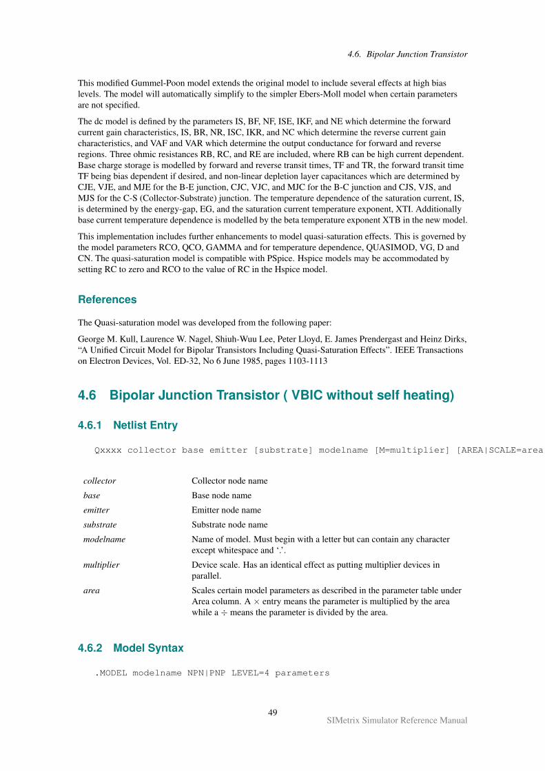
4.6. Bipolar Junction Transistor
This modified Gummel-Poon model extends the original model to include several effects at high biaslevels. The model will automatically simplify to the simpler Ebers-Moll model when certain parametersare not specified.
The dc model is defined by the parameters IS, BF, NF, ISE, IKF, and NE which determine the forwardcurrent gain characteristics, IS, BR, NR, ISC, IKR, and NC which determine the reverse current gaincharacteristics, and VAF and VAR which determine the output conductance for forward and reverseregions. Three ohmic resistances RB, RC, and RE are included, where RB can be high current dependent.Base charge storage is modelled by forward and reverse transit times, TF and TR, the forward transit timeTF being bias dependent if desired, and non-linear depletion layer capacitances which are determined byCJE, VJE, and MJE for the B-E junction, CJC, VJC, and MJC for the B-C junction and CJS, VJS, andMJS for the C-S (Collector-Substrate) junction. The temperature dependence of the saturation current, IS,is determined by the energy-gap, EG, and the saturation current temperature exponent, XTI. Additionallybase current temperature dependence is modelled by the beta temperature exponent XTB in the new model.
This implementation includes further enhancements to model quasi-saturation effects. This is governed bythe model parameters RCO, QCO, GAMMA and for temperature dependence, QUASIMOD, VG, D andCN. The quasi-saturation model is compatible with PSpice. Hspice models may be accommodated bysetting RC to zero and RCO to the value of RC in the Hspice model.
References
The Quasi-saturation model was developed from the following paper:
George M. Kull, Laurence W. Nagel, Shiuh-Wuu Lee, Peter Lloyd, E. James Prendergast and Heinz Dirks,“A Unified Circuit Model for Bipolar Transistors Including Quasi-Saturation Effects”. IEEE Transactionson Electron Devices, Vol. ED-32, No 6 June 1985, pages 1103-1113
4.6 Bipolar Junction Transistor ( VBIC without self heating)
4.6.1 Netlist Entry
Qxxxx collector base emitter [substrate] modelname [M=multiplier] [AREA|SCALE=area]
collector Collector node name
base Base node name
emitter Emitter node name
substrate Substrate node name
modelname Name of model. Must begin with a letter but can contain any characterexcept whitespace and ‘.’.
multiplier Device scale. Has an identical effect as putting multiplier devices inparallel.
area Scales certain model parameters as described in the parameter table underArea column. A × entry means the parameter is multiplied by the areawhile a ÷ means the parameter is divided by the area.
4.6.2 Model Syntax
.MODEL modelname NPN|PNP LEVEL=4 parameters
49SIMetrix Simulator Reference Manual
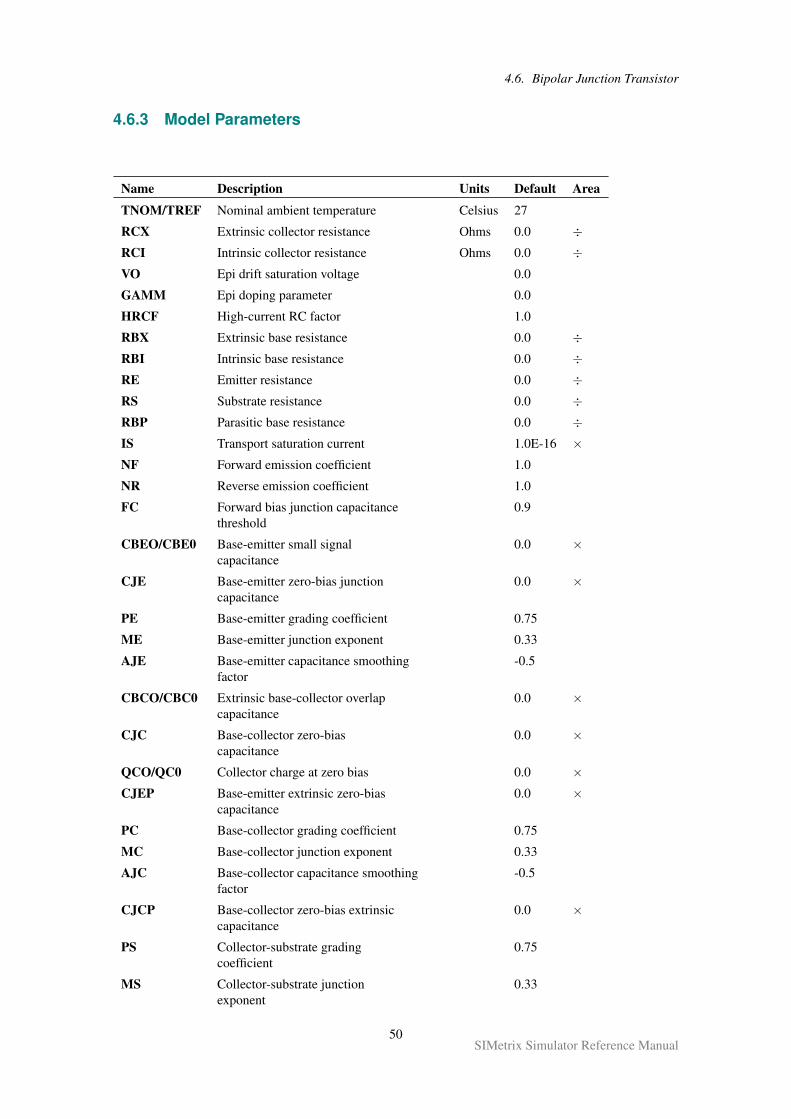
4.6. Bipolar Junction Transistor
4.6.3 Model Parameters
Name Description Units Default Area
TNOM/TREF Nominal ambient temperature Celsius 27
RCX Extrinsic collector resistance Ohms 0.0 ÷RCI Intrinsic collector resistance Ohms 0.0 ÷VO Epi drift saturation voltage 0.0
GAMM Epi doping parameter 0.0
HRCF High-current RC factor 1.0
RBX Extrinsic base resistance 0.0 ÷RBI Intrinsic base resistance 0.0 ÷RE Emitter resistance 0.0 ÷RS Substrate resistance 0.0 ÷RBP Parasitic base resistance 0.0 ÷IS Transport saturation current 1.0E-16 ×NF Forward emission coefficient 1.0
NR Reverse emission coefficient 1.0
FC Forward bias junction capacitancethreshold
0.9
CBEO/CBE0 Base-emitter small signalcapacitance
0.0 ×
CJE Base-emitter zero-bias junctioncapacitance
0.0 ×
PE Base-emitter grading coefficient 0.75
ME Base-emitter junction exponent 0.33
AJE Base-emitter capacitance smoothingfactor
-0.5
CBCO/CBC0 Extrinsic base-collector overlapcapacitance
0.0 ×
CJC Base-collector zero-biascapacitance
0.0 ×
QCO/QC0 Collector charge at zero bias 0.0 ×CJEP Base-emitter extrinsic zero-bias
capacitance0.0 ×
PC Base-collector grading coefficient 0.75
MC Base-collector junction exponent 0.33
AJC Base-collector capacitance smoothingfactor
-0.5
CJCP Base-collector zero-bias extrinsiccapacitance
0.0 ×
PS Collector-substrate gradingcoefficient
0.75
MS Collector-substrate junctionexponent
0.33
50SIMetrix Simulator Reference Manual
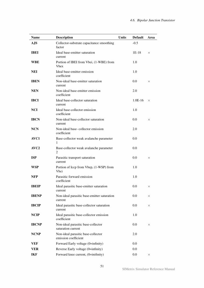
4.6. Bipolar Junction Transistor
Name Description Units Default Area
AJS Collector-substrate capacitance smoothingfactor
-0.5
IBEI Ideal base-emitter saturationcurrent
1E-18 ×
WBE Portion of IBEI from Vbei, (1-WBE) fromVbex
1.0
NEI Ideal base-emitter emissioncoefficient
1.0
IBEN Non-ideal base-emitter saturationcurrent
0.0 ×
NEN Non-ideal base-emitter emissioncoefficient
2.0
IBCI Ideal base-collector saturationcurrent
1.0E-16 ×
NCI Ideal base-collector emissioncoefficient
1.0
IBCN Non-ideal base-collector saturationcurrent
0.0 ×
NCN Non-ideal base- collector emissioncoefficient
2.0
AVC1 Base-collector weak avalanche parameter1
0.0
AVC2 Base-collector weak avalanche parameter2
0.0
ISP Parasitic transport saturationcurrent
0.0 ×
WSP Portion of Iccp from Vbep, (1-WSP) fromVbci
1.0
NFP Parasitic forward emissioncoefficient
1.0
IBEIP Ideal parasitic base-emitter saturationcurrent
0.0 ×
IBENP Non-ideal parasitic base-emitter saturationcurrent
0.0 ×
IBCIP Ideal parasitic base-collector saturationcurrent
0.0 ×
NCIP Ideal parasitic base-collector emissioncoefficient
1.0
IBCNP Non-ideal parasitic base-collectorsaturation current
0.0 ×
NCNP Non-ideal parasitic base-collectoremission coefficient
2.0
VEF Forward Early voltage (0=infinity) 0.0
VER Reverse Early voltage (0=infinity) 0.0
IKF Forward knee current, (0=inifinity) 0.0 ×
51SIMetrix Simulator Reference Manual
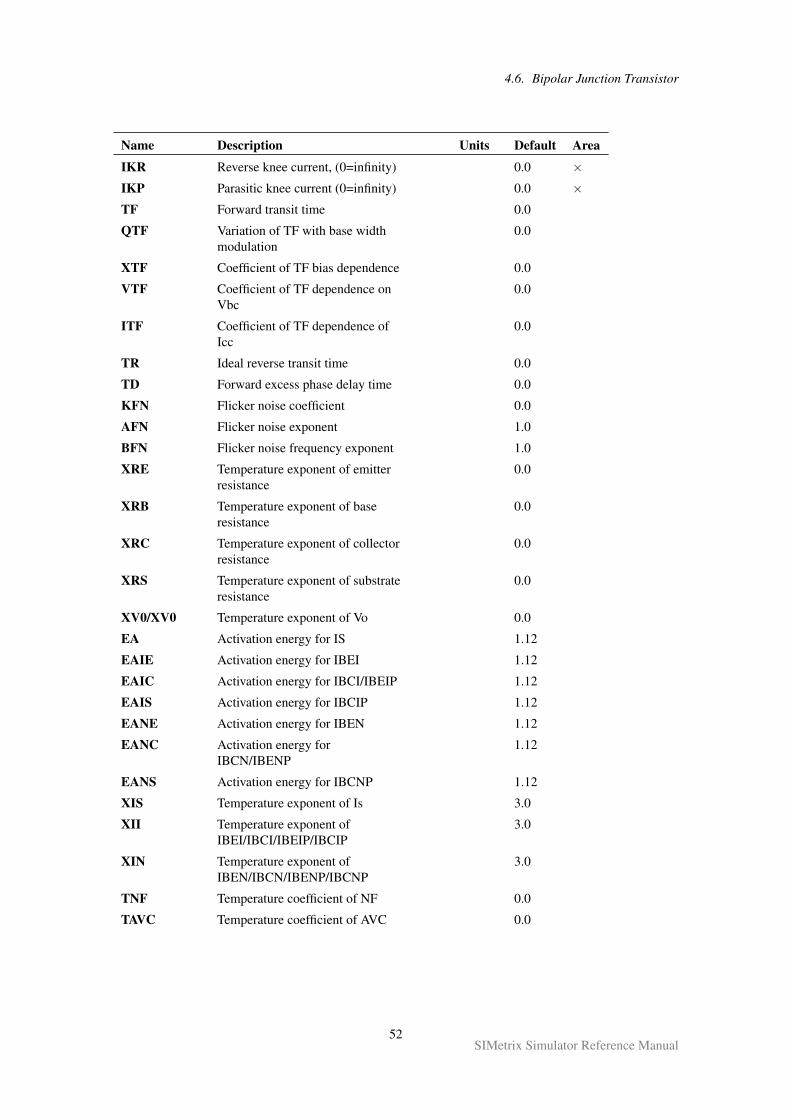
4.6. Bipolar Junction Transistor
Name Description Units Default Area
IKR Reverse knee current, (0=infinity) 0.0 ×IKP Parasitic knee current (0=infinity) 0.0 ×TF Forward transit time 0.0
QTF Variation of TF with base widthmodulation
0.0
XTF Coefficient of TF bias dependence 0.0
VTF Coefficient of TF dependence onVbc
0.0
ITF Coefficient of TF dependence ofIcc
0.0
TR Ideal reverse transit time 0.0
TD Forward excess phase delay time 0.0
KFN Flicker noise coefficient 0.0
AFN Flicker noise exponent 1.0
BFN Flicker noise frequency exponent 1.0
XRE Temperature exponent of emitterresistance
0.0
XRB Temperature exponent of baseresistance
0.0
XRC Temperature exponent of collectorresistance
0.0
XRS Temperature exponent of substrateresistance
0.0
XV0/XV0 Temperature exponent of Vo 0.0
EA Activation energy for IS 1.12
EAIE Activation energy for IBEI 1.12
EAIC Activation energy for IBCI/IBEIP 1.12
EAIS Activation energy for IBCIP 1.12
EANE Activation energy for IBEN 1.12
EANC Activation energy forIBCN/IBENP
1.12
EANS Activation energy for IBCNP 1.12
XIS Temperature exponent of Is 3.0
XII Temperature exponent ofIBEI/IBCI/IBEIP/IBCIP
3.0
XIN Temperature exponent ofIBEN/IBCN/IBENP/IBCNP
3.0
TNF Temperature coefficient of NF 0.0
TAVC Temperature coefficient of AVC 0.0
52SIMetrix Simulator Reference Manual
4.7. Bipolar Junction Transistor
4.6.4 Notes
The VBIC model is only available with Elite versions.
The Vertical Bipolar Inter-Company (VBIC) model is an advanced bipolar junction transistor model. Thisis the 4-terminal non-thermal version. There is also a version that supports self-heating effects and has 5terminals, see “Bipolar Junction Transistor (VBIC with self heating)” on page 53.
For more information about VBIC, please refer to this link:
VBIC Reference
4.7 Bipolar Junction Transistor (VBIC with self heating)
4.7.1 Netlist Entry
Qxxxx collector base emitter substrate thermal_node modelname[M=multiplier] [AREA|SCALE=area]
collector Collector node name
base Base node name
emitter Emitter node name
substrate Substrate node name
thermal_node See notes
modelname Name of model. Must begin with a letter but can contain any characterexcept whitespace and ‘.’ .
multiplier Device scale. Has an identical effect as putting multiplier devices inparallel.
area Scales certain model parameters as described in the parameter table underArea column. A∞ entry means the parameter is multiplied by the areawhile a means the parameter is divided by the area.
4.7.2 Model Syntax
.MODEL modelname NPN|PNP LEVEL=1004 parameters
4.7.3 Model Parameters
Model parameters are identical to the non-thermal version except for the addition of the following:
Name Description Units Default Area
RTH Thermal resistance 0.0 ÷CTH Thermal capacitance 0.0 ×
4.7.4 Notes
The VBIC model is only available with Elite versions.
53SIMetrix Simulator Reference Manual
4.9. Bipolar Junction Transistor
This model is the same as the VBIC non-thermal model except for the addition of self-heating effects. Usethe non-thermal version if you do not need self-heating as its implementation is simpler and will run faster.
The thermal_node may be used to connect external thermal networks to model thermal flow. Power inwatts is represented by current and temperature rise in Kelvin is represented by the voltage. Note that thevoltage is temperature rise above the simulation temperature, not an absolute value.
4.8 Bipolar Junction Transistor (MEXTRAM)
See “NXP Compact Models” on page 126.
4.9 Bipolar Junction Transistor (HICUM)
4.9.1 Netlist Entry
Qxxxx collector base emitter [substrate] modelname
Where:
collector Collector node
base Base node
emitter Emitter node
substrate Substrate node
modelname Model name as used with .MODEL statement
4.9.2 NPN Model Syntax
.MODEL modelname NPN LEVEL=8 parameters
OR
.MODEL modelname HICUM_211 PNP=0 parameters
4.9.3 PNP Model Syntax
.MODEL modelname PNP LEVEL=8 parameters
OR
.MODEL modelname HICUM_211 PNP=1 parameters
4.9.4 Notes
The model provided is “Level 2 version 2.11”.
The model was implemented from Verilog-A code. It has received only minor changes from the originalsupplied by the developers. These changes are to implement PNP devices and to overcome a problem inthe original model whereby it is possible for it to converge to an erroneous state.
The SIMetrix implementation of this model has been tested using the benchmark results provided by thedevelopers. The majority of the tests showed a match of better than 0.1%. A few were over 1% with onedeviating by 7%. These were investigated and it was found that the reference data was in error probablybecause of insufficient convergence tolerance.
54SIMetrix Simulator Reference Manual
4.10. Capacitor
4.10 Capacitor
4.10.1 Netlist Entry
Cxxxx n1 n2 [model_name] value [IC=initial_condition] [TEMP=local_temp][TC1=tc1] [TC2=tc2] [VC1=vc1] [VC2=vc2] [BRANCH=0|1] [M=mult] [DTEMP=dtemp][ESR=esr]
n1 Node 1
n2 Node 2
model_name (Optional) Name of model. Must begin with a letter but can contain anycharacter except whitespace and period ‘.’
value Capacitance (Farads)
initial_condition Initial voltage if UIC specified on .TRAN statement.
local_temp Capacitor temperature (°C)
tc1 First order temperature coefficient
tc2 Second order temperature coefficient
vc1 First order voltage coefficient
vc2 Second order voltage coefficient
BRANCH May be 0 or 1. 0 is the default. This parameter determines the internalformulation of the capacitor and affects how the IC parameter isimplemented. When BRANCH=0, the capacitor looks like an open circuitduring the DC operating point and the IC parameter has no effect unlessUIC is specified for a transient analysis. If BRANCH=1, the capacitorlooks like a voltage source during dc operating point with a magnitudeequal to the value of the IC parameter. BRANCH=1 makes it possible tospecify circuit startup conditions. See “Alternative Initial ConditionImplementations” on page 205 for an example.
mult Device multiplier. Equivalent to putting mult devices in parallel.
dtemp Differential temperature. Similar to local_temp but is specified relative tocircuit temperature. If both TEMP and DTEMP are specified, TEMP takesprecedence.
esr Effective series resistance. If non-zero (the default value), a resistor ofvalue esr will be connected in series with the capacitor. The resultingimplementation of a series RC network is more efficient and offers betterconvergence than using a separate R and C. This is especially the case ifthe capacitor has a high value and is non-grounded.
Important: this resistor is noiseless; if the noise in the ESR is importantin your design, you should use a separate resistor and omit this parameterin the capacitor.
4.10.2 Model Syntax
.model modelname CAP ( parameters )
4.10.3 Model Parameters
55SIMetrix Simulator Reference Manual
4.11. Controlled Current Source
Name Description Units Default
C Capacitor multiplier 1
TC1 First order temperature coefficient 1/°C 0
TC2 Second order temperaturecoefficient
1/°C2 0
VC1 First order voltage coefficient Volt-1 0
VC2 Second order voltage coefficient Volt-2 0
TNOM, T_MEASURED Reference temperature; the temperature atwhich the model parameters weremeasured
C 27
T_ABS If specified, defines the absolute modeltemperature overriding the globaltemperature defined using .TEMP
C -
T_REL_GLOBAL Offsets global temperature defined using.TEMP. Overridden by T_ABS
C 0.0
4.11 Current Controlled Current Source
4.11.1 Netlist Entry
Linear Source
Fxxxx nout+ nout- vc current_gain
nout+ Positive output node
nout- Negative output node
vc Controlling voltage source
current_gain Output current/Input current
SPICE2 polynomial sources are also supported in order to maintain compatibility with commerciallyavailable libraries for IC’s. (Most operational amplifier models for example use several polynomialsources). In general, however the arbitrary source (see “Arbitrary Source” on page 39) is more flexible andeasier to use.
Polynomial Source
Fxxxx nout+ nout- POLY( num_inputs ) vc1 vc2 ...+ polynomial_specification
vc1, vc2 Controlling voltage sources
num_inputs Number of controlling currents for source.
polynomial_specification See “Polynomial Specification” on page 57.
56SIMetrix Simulator Reference Manual
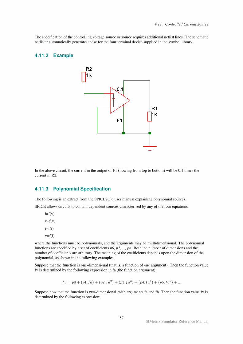
4.11. Controlled Current Source
The specification of the controlling voltage source or source requires additional netlist lines. The schematicnetlister automatically generates these for the four terminal device supplied in the symbol library.
4.11.2 Example
In the above circuit, the current in the output of F1 (flowing from top to bottom) will be 0.1 times thecurrent in R2.
4.11.3 Polynomial Specification
The following is an extract from the SPICE2G.6 user manual explaining polynomial sources.
SPICE allows circuits to contain dependent sources characterised by any of the four equations
i=f(v)
v=f(v)
i=f(i)
v=f(i)
where the functions must be polynomials, and the arguments may be multidimensional. The polynomialfunctions are specified by a set of coefficients p0, p1, ..., pn. Both the number of dimensions and thenumber of coefficients are arbitrary. The meaning of the coefficients depends upon the dimension of thepolynomial, as shown in the following examples:
Suppose that the function is one-dimensional (that is, a function of one argument). Then the function valuefv is determined by the following expression in fa (the function argument):
fv = p0 + (p1.fa) + (p2.fa2) + (p3.fa3) + (p4.fa4) + (p5.fa5) + ...
Suppose now that the function is two-dimensional, with arguments fa and fb. Then the function value fv isdetermined by the following expression:
57SIMetrix Simulator Reference Manual
4.12. Current Controlled Voltage Source
fv = p0 + (p1.fa) + (p2.fb) + (p3.fa2) + (p4.fa.fb) + (p5.fb2)
+(p6.fa3) + (p7.fa2.fb) + (p8.fa.fb2) + (p9.fb3) + ...
Consider now the case of a three-dimensional polynomial function with arguments fa, fb, and fc. Then thefunction value fv is determined by the following expression:
fv = p0 + (p1.fa) + (p2.fb) + (p3.fc) + (p4.fa2) + (p5.fa.fb) + (p6.fa.fc) + (p7.fb2) + (p8.fb.fc)
+(p9.fc2) + (p10.fa3) + (p11.fa2.fb) + (p12.fa2.fc) + (p13.fa.fb2) + (p14.fa.fb.fc)
+(p15.fa.fc2) + (p16.fb3) + (p17.fb2.fc) + (p18.fb.fc2) + (p19.fc3) + (p20.fa4) + ...
Note If the polynomial is one-dimensional and exactly one coefficient isspecified, then SPICE assumes it to be p1 (and p0 = 0.0), in order tofacilitate the input of linear controlled sources.
4.12 Current Controlled Voltage Source
4.12.1 Netlist Entry
Linear Source
Hxxxx nout+ nout- vc transresistance
nout+ Positive output node
nout- Negative output node
vc Controlling voltage source
transresistance Output current/Input current (Ω)
SPICE2 polynomial sources are also supported in order to maintain compatibility with commerciallyavailable libraries for IC’s. (Most Op-amp models use several polynomial sources). In general, howeverthe arbitrary source is more flexible and easier to use.
Polynomial Source
Hxxxx nout+ nout- POLY( num_inputs ) vc1 vc2 ...+ polynomial_specification
vc1, vc2 Controlling voltage sources
num_inputs Number of controlling currents for source.
polynomial_specification See “Polynomial Specification” on page 57.
The specification of the controlling voltage source or source requires additional netlist lines. The schematicnetlister automatically generates these for the four terminal device supplied in the symbol library.
58SIMetrix Simulator Reference Manual
4.14. Diode - Level 1 and Level 3
4.13 Current Source
4.13.1 Netlist Entry
Ixxxx n+ n- [DC dcvalue] [AC magnitude [phase]] [transient_spec]
n+ Positive node
n- Negative node
dcvalue Value of source for dc operating point analysis
magnitude AC magnitude for AC sweep analysis.
phase phase for AC sweep analysis
transient_spec Specification for time varying source. Can be one of following:
Pulse see “Pulse Source” on page 113
Piece wise linear see “Piece-Wise Linear Source” on page 115
Sine see “Sinusoidal Source” on page 116
Exponential see “Exponential Source” on page 117
Single frequency FM see “Single Frequency FM” on page 118
Extended PWL Source see “Extended PWL Source” on page 118
4.14 Diode - Level 1 and Level 3
4.14.1 Netlist Entry
Dxxxx n+ n- model_name [area] [OFF] [IC=vd] [TEMP=local_temp]+ [PJ=periphery] [L=length] [W=width] [M=mult] [DTEMP=dtemp]
n+ Anode
n- Cathode
model_name Name of model defined in a .MODEL statement. Must begin with a letterbut can contain any character except whitespace and ‘.’.
area Area multiplying factor. Area scales up the device. E.g. an area of 3 wouldmake the device behave like 3 diodes in parallel. Default is 1.
OFF Instructs simulator to calculate operating point analysis with deviceinitially off. This is used in latching circuits such as thyristors andbistables to induce a particular state. See “.OP” on page 220 for moredetails.
vd Initial condition for diode voltage. This only has an effect if the UICparameter is specified on the .TRAN statement.
local_temp Local temperature. Overrides specification in .OPTIONS or .TEMPstatements.
periphery Level 3 only. Junction periphery used for calculating sidewalleffects.
length Level 3 only. Used to calculate area. See below.
width Level 3 only. Used to calculate area. See below.
59SIMetrix Simulator Reference Manual
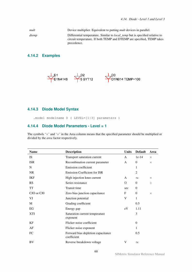
4.14. Diode - Level 1 and Level 3
mult Device multiplier. Equivalent to putting mult devices in parallel.
dtemp Differential temperature. Similar to local_temp but is specified relative tocircuit temperature. If both TEMP and DTEMP are specified, TEMP takesprecedence.
4.14.2 Examples
4.14.3 Diode Model Syntax
.model modelname D ( LEVEL=[1|3] parameters )
4.14.4 Diode Model Parameters - Level = 1
The symbols ‘×’ and ‘÷’ in the Area column means that the specified parameter should be multiplied ordivided by the area factor respectively.
Name Description Units Default Area
IS Transport saturation current A 1e-14 ×ISR Recombination current parameter A 0 ×N Emission coefficient 1
NR Emission Coefficient for ISR 2
IKF High injection knee current A ∞ ×RS Series resistance Ω 0 ÷TT Transit time sec 0
CJO or CJ0 Zero bias junction capacitance F 0 ×VJ Junction potential V 1
M Grading coefficient 0.5
EG Energy gap eV 1.11
XTI Saturation current temperatureexponent
3
KF Flicker noise coefficient 0
AF Flicker noise exponent 1
FC Forward bias depletion capacitancecoefficient
0.5
BV Reverse breakdown voltage V ∞
60SIMetrix Simulator Reference Manual
4.14. Diode - Level 1 and Level 3
Name Description Units Default Area
IBV Current at breakdown voltage A 1e-10 ×TNOM, T_MEASURED Parameter measurement
temperature°C 27
T_ABS If specified, defines the absolute modeltemperature overriding the globaltemperature defined using .TEMP
°C -
T_REL_ GLOBAL Offsets global temperature defined using.TEMP. Overridden by T_ABS
°C 0
TRS1 First order tempco RS /°C 0
TRS2 Second order tempco RS /°C2 0
TBV1 First order tempco BV /°C 0.0
TBV2 Second order tempco BV /°C2 0.0
NBV Reverse breakdown ideality factor 1.0
NBVL Low-level reverse breakdown idealityfactor
1.0
IBVL Low-level reverse breakdown kneecurrent
Amp 0.0 ×
TIKF IKF temperature coefficient 0.0
Notes The dc characteristics of the diode are determined by the parameters IS, N, ISR, NRand IKF. An ohmic resistance, RS, is included. Charge storage effects are modelledby a transit time, TT, and a non-linear depletion layer capacitance which isdetermined by the parameters CJO, VJ, and M. The temperature dependence of thesaturation current is defined by the parameters EG, the energy and XTI, thesaturation current temperature exponent. Reverse breakdown is modelled by anexponential increase in the reverse diode current and is determined by the parametersBV and IBV (both of which are positive numbers).
4.14.5 Diode Model Parameters - Level = 3
Name Description Units Default
AF Flicker noise exponent 1.0
BV, VB, VAR, VRB Reverse breakdown voltage V ∞CJO, CJ Zero bias junction capacitance F 0.0
CJSW, CJP Zero bias sidewall capacitance F 0.0
CTA CJO temp coefficient. (TLEVC=1) °C−1
CTP CJSW temp coefficient.(TLEVC=1)
°C−1
EG Energy gap ev 1.11
FC Forward bias depletion capacitancecoefficient
0.5
61SIMetrix Simulator Reference Manual
4.14. Diode - Level 1 and Level 3
Name Description Units Default
FCS Forward bias sidewall capacitancecoefficient
0.5
GAP1 7.02e-4 - silicon (old value)
4.73e-4 - silicon
4.56e-4 - germanium
5.41e-4 - gallium arsenide
eV/° 7.02e-4
GAP2 1108 - silicon (old value)
636 - silicon
210 - germanium
204 - gallium arsenide
° 1108
IBV Current at breakdown voltage A 1E-3
IKF, IK High injection knee current A ∞IKR Reverse high injection knee
currentA ∞
IS, JS Saturation current A 1E-14
ISR Recombination current A 0
JSW Sidewall saturation current A 0
KF Flicker noise exponent 0
MJ, M Grading coefficient 0.5
MJSW Sidewall grading coefficient 0.33
N, NF Forward emission coefficient 1.0
NR Recombination emissioncoefficient
2.0
PHP Sidewall built in potential PB
RS Series resistance Ω 0
SHRINK Shrink factor 1.0
TCV BV temp coefficient °C-1 0
TLEV Temperature model selector. Valid values:0, 1, 2
0
TLEVC Temperature model selector. Valid values:0 or 1
0
TNOM, TREF Parameter measurementtemperature
27
TPB VJ temp coefficient (TLEVC=1) V/°C 0.0
TPHP PHP temp. coefficient (TLEVC=1) V/°C 0.0
TRS RS temp. coefficient °C−1 0.0
TT Transit time S 0.0
VJ, PB Built-in potential V 0.8
XW Shrink factor 0.0
DCAP Capacitance model (1 or 2) 1
62SIMetrix Simulator Reference Manual
4.15. Diode - Soft Recovery
The parameters CJSW and JSW are scaled by the instance parameter PJ whose default value is 0.0.
If L and W instance parameters are supplied, the diode is scaled by the factor:M*(L*SHRINK-XW)*(W*SHRINK-XW) otherwise it is scaled by M*AREA.
4.14.6 Using Hspice Diodes
In Hspice Level 1 diodes are the same as the SIMetrix Level 3 diode. To map Level 3 to Level 1, add thisline to the netlist
.OPTIONS HSPICEMODELS=1
This setting also has the same effect:
.OPTIONS HSPICECOMPATIBILITY=1
See “.OPTIONS” on page 222 for more details
M and AREA are instance parameters which default to 1.0
4.15 Diode - Soft Recovery
4.15.1 Netlist Entry
Dxxxx n+ n- model_name [TEMP=local_temp]
n+ Anode
n- Cathode
model_name Name of model defined in a .MODEL statement. Must begin with a letterbut can contain any character except whitespace and ‘.’.
local_temp Local temperature. Overrides specification in .OPTIONS or .TEMPstatements.
4.15.2 Diode Model Syntax
.model modelname SRDIO ( parameters )
4.15.3 Soft Recovery Diode Model Parameters
Name Description Units Default
CJO Zero bias junction capacitance F 0.0
EG Energy gap ev 1.11
FC Forward bias depletion capacitance coefficient 0.5
IS Saturation current A 1E-15
MJ Grading coefficient 0.5
N Forward emission coefficient 1.0
RS Series resistance Ω 0
63SIMetrix Simulator Reference Manual
4.16. GaAsFET
Name Description Units Default
TNOM Parameter measurement temperature 27
TT Diffusion transit time S 5e-6
TAU Minority carrier lifetime 1e-5
VJ Built-in potential V 1
XTI Saturation current temperature exponent 3
4.15.4 Basic Equations
The model is based on the paper “A Simple Diode Model with Reverse Recovery” by Peter Lauritzen andCliff Ma. (See references). The model’s governing equations are quite simple and are as follows:
id =qe − qmTT
dqmdt
+qmTAU
− qe − qmTT
= 0
qe = IS · TAU ·(
exp
(vd
N · Vt
)− 1
)In addition the model uses the standard SPICE equations for junction capacitance and temperaturedependence of IS.
4.15.5 References
Peter O. Lauritzen, Cliff L. Ma, A Simple Diode Model with Reverse Recovery, IEEE Transactions onPower Electronics, Vol. 6, No 2, pp 188-191, April 1991.
4.16 GaAsFET
4.16.1 Netlist Entry
Zxxxx drain gate source modelname [area] [OFF] [IC=vds, vgs]
drain Drain node
gate Gate node
source Source node
modelname Name of model defined in a .model statement. Must begin with a letter butcan contain any character except whitespace and period ‘.’ .
area Area multiplying factor. Area scales up the device. E.g. an area of 3 wouldmake the device behave like 3 transistors in parallel. Default is one.
OFF Instructs simulator to calculate operating point analysis with deviceinitially off. This is used in latching circuits such as thyristors andbistables to induce a particular state. See “.OP” on page 220 for moredetails.
64SIMetrix Simulator Reference Manual
4.17. Inductor (Ideal)
vds,vgs Initial conditions for drain-source and gate-source junctions respectively.These only have an effect if the UIC parameter is specified on the .TRANstatement.
4.16.2 GaAsFET Model Syntax
.model modelname NMF ( parameters )
4.16.3 GaAsFET Model Parameters
The symbols ‘×’ and ‘÷’ in the Area column means that parameter should be multiplied or divided by thearea factor respectively.
Name Description Units Default Area
VTO Pinch-off Voltage V -2.0
BETA Transconductance parameter A/V2 2.5e-3 ×B Doping tail extending parameter 1/V 0.3
ALPHA Saturation voltage parameter 1/V 2
LAMBDA Channel length modulation parameter 1/V 0
RD Drain ohmic resistance Ω 0 ÷RS Source ohmic resistance Ω 0 ÷CGS Zero bias gate source capacitance F 0 ×CGD Zero bias gate drain capacitance F 0 ×PB Gate junction potential V 1
IS Gate p-n saturation current A 1e-14 ×FC Forward bias depletion capacitance coefficient 0.5
KF Flicker noise coefficient 0
AF Flicker noise exponent 1
Notes The GaAsFET model is derived from the model developed by Statz. The DCcharacteristics are defined by parameters VTO, B and BETA, which determine thevariation of drain current with gate voltage, ALPHA, which determines saturationvoltage, and LAMBDA, which determines the output conductance. IS determines thegate-source and gate-drain dc characteristics.
Two ohmic resistances are included. Charge storage is modelled by total gate chargeas a function of gate-drain and gate-source voltages and is defined by the parametersCGS, CGD and PB.
4.17 Inductor (Ideal)
4.17.1 Netlist Entry
Lxxxx n1 n2 value [IC=init_cond] [BRANCH=0|1]
65SIMetrix Simulator Reference Manual
4.18. Inductor (Saturable)
n1 Node 1
n2 Node 2
value Value in henries
init_cond Initial current in inductor. Only effective if UIC option is specified on.TRAN statement.
BRANCH set to 0 or 1. 1 is default value. This parameter determines the internalformulation of the inductor and affects how the IC parameter isimplemented. When BRANCH=1, the inductor looks like a short circuitduring DC operating point and the IC parameter has no effect unless UICis specified for a transient analysis. If BRANCH=0, the inductor looks likea current source during dc operating point with a magnitude equal to thevalue of the IC parameter. BRANCH=0 makes it possible to specifycircuit startup conditions.
4.17.2 See Also
“Mutual Inductor” on page 120.
4.18 Inductor (Saturable)
4.18.1 Netlist Entry
Lxxxx n1 n2 modelname [N=num_turns] [LE=le] [AE=ae] [UE=ue]
n1 Node 1
n2 Node 2
modelname Model name referring to a .MODEL statement describing the corecharacteristics. See details below.
num_turns Number of turns on winding
le Effective path length of core in metres. Default = PATH/100. PATH isdefined in .MODEL.
ae Effective area of core in metres2. Default = AREA/10000 where AREA isdefine in .MODEL.
ue Effective permeability of core. Overrides model parameter of the samename.
4.18.2 Model format - Jiles-Atherton model with hysteresis
.MODEL model_name CORE parameters
4.18.3 Model format - simple model without hysteresis
.MODEL model_name CORENH parameters
4.18.4 Jiles-Atherton Parameters
66SIMetrix Simulator Reference Manual
4.18. Inductor (Saturable)
Name Description Units Default
PATH Effective path length cm 1
C Domain flexing parameter 0.2
K Domain anisotropy parameter amp.m-1 500
MS Magnetisation saturation 1E6
GAP Air gap (centimetres) cm 0
GAPM Air gap (metres) m GAP/100
A Thermal energy parameter amp.m-1 1000
AREA Effective area cm2 0.1
UE Effective permeability. Overrides GAP and GAPM if>0. See notes
AHMODE Anhysteric function selector (see notes) 0
4.18.5 Non-hysteresis Model Parameters
Name Description Units Default
PATH Effective path length cm 1
MS Magnetisation saturation 1E6
GAP Air gap (centimetres) cm 0
GAPM Air gap (metres) m GAP/100
A Thermal energy parameter amp.m-1 1000
AREA Effective area cm2 0.1
AHMODE Anhysteric function selector (see notes) 0
4.18.6 Notes on the Jiles-Atherton model
The Jiles-Atherton model is based on the theory developed by D.C. Jiles and D.L. Atherton in their 1986paper “Theory of Ferromagnetic Hysteresis”. The model has been modified to correct non-physicalbehaviour observed at the loop tips whereby the slope of the B-H curve reverses. This leads tonon-convergence in the simulator. The modification made is that proposed by Lederer et al. (See referencesbelow). Full details of the SIMetrix implementation of this model including all the equations are providedin a technical note. This is located on the install CDROM at Docs/Magnetics/Jiles-Atherton-Model.pdf.This is also available at our web site, please visit “Further Documentation” on page 38 for details.
The AHMODE parameter selects the equation used for the anhysteric function, that is the non-linear curvedescribing the saturating behaviour. When set to 0 the function is the same as that used by PSpice. Whenset to 1 the function is the original equation proposed by Jiles and Atherton. See theJiles-Atherton-Model.pdf technical note for details.
If the UE parameters is specified either on the device line or in the model, an air gap value is calculatedand the parameters GAP and GAPM are ignored. See the Jiles-Atherton-Model.pdf technical note for theformula used.
The parameter names and their default values for the Jiles-Atherton model are compatible with PSpice, butthe netlist entry is different.
67SIMetrix Simulator Reference Manual
4.19. Inductor (Table lookup)
4.18.7 Notes on the non-hysteresis model
This is simply a reduced version of the Jiles-Atherton model with the hysteresis effects removed. Theanhysteric function and the air-gap model are the same as the Jiles-Atherton model.
4.18.8 Implementing Transformers
This model describes only a 2 terminal inductor. A transformer can be created using a combination ofcontrolled sources along with a single inductor. The SIMetrix schematic editor uses this method.
The schematic editor provides a means of creating transformers and this uses an arrangement of controlledsources to fabricate a non-inductive transformer. Any inductor can be added to this arrangement to createan inductive transformer. The method is simple and efficient. The following shows how a non-inductivethree winding transformer can be created from simple controlled sources:
F1 0 n1 E1 1E1 W1A W1B n1 0 1F2 0 n1 E2 1E2 W2A W2B n1 0 1F3 0 n1 E3 1E3 W3A W3B n1 0 1
Connecting an inductor between n1 and 0 in the above provides the inductive behaviour. This is in facthow the SIMetrix schematic editor creates non-linear transformers.
Note that you cannot use the mutual inductor device with the saturable inductor.
4.18.9 Plotting B-H curves
Both models can be enabled to output values for flux density in Tesla and magnetising force in A.m-1. Todo this, add the following line to the netlist:
.KEEP Lxxx#B Lxxx#H
Replace Lxxx with the reference for the inductor. (e.g. L23 etc.). You will find vectors with the namesLxxx#B Lxxx#H available for plotting in the waveform viewer.
4.18.10 References
1. Theory of Ferromagnetic Hysteresis, DC.Jiles, D.L. Atherton, Journal of Magnetism and MagneticMaterials, 1986 p48-60.
2. On the Parameter Identification and Application of the Jiles-Atherton Hysteresis Model forNumerical Modelling of Measured Characteristics, D Lederer, H Igarashi, A Kost and T Honma,IEEE Transactions on Magnetics, Vol. 35, No. 3, May 1999
4.19 Inductor (Table lookup)
4.19.1 Netlist Entry
Uxxxx n1 n2 model_name [IC=initial_condition] [USEIC=use_ic]
68SIMetrix Simulator Reference Manual
4.19. Inductor (Table lookup)
n1 node 1
n2 node 2
initial_condition Initial condition in Amps. Only active if USEIC is non-zero
use_ic If non-zero, enable initial condition. This will set the current in theinductor to the value of initial_condition during the DC operating pointanalysis
4.19.2 Model syntax
.MODEL model_name TABLE_INDUCTOR parameters
Name Description Units Default
L Inductance 1m H
LTABLE Saturation table n/a
ITABLE Current table A n/a
TABLE_SIZE Number of elements in tables 2
RSERIES Series resistance Ω 0.0
RSHUNT Shunt resistance Ω 0.0 (sets to INF)
LMIN Minimum inductance H 0.0
SMOOTH Smoothing option (0-3) 0
Model Example
.MODEL TABLE_IND table_inductor L=1 USEIC=0 IC=0+ RSERIES=0 RSHUNT=0 SMOOTH=2 TABLE_SIZE=7+ ITABLE=[0, 8.3333, 16.666, 25, 33.3333, 41.666, 50]+ LTABLE=[3.36e-07, 3.36e-07, 3.34e-07, 3.27e-07, 3.09e-07, 1.86e-07, 4.21e-08]
The above example has an inductance of 3.36e-07H at 0A falling to 4.21e-08 at 50A.
4.19.3 Boundary Inductance
The inductance for this device is defined by a lookup table over a specific range. However, the behaviourat currents beyond that defined in the table must also be defined. We refer to the inductance as the‘boundary inductance’. This follows a characteristic of the form:
A/(C + i2) + LMIN/L
Where A and C are chosen so that the absolute inductance and dLdi matches the table function at the final
point.
4.19.4 Smoothing Function
The SMOOTH parameter can be set to an integer between 1 and 4 to select a smoothing function. Thefollowing table describes the alternative strategies available:
69SIMetrix Simulator Reference Manual
4.20. IGBT
SMOOTH value Function
0 No smoothing function is selected. Inductor follows a PWL(piece-wise-linear) characteristic
1 Local cubic. Fits a cubic polynomial between each pair of points such thatthe gradient at each point is the average of the slope on either side of thepoint. This is continuous in the first derivative but is not continuous in thesecond derivative
2 Cubic spline with boundary conditions:lower: dLdi = 0
upper: d2Ldi2 = 0
3 Cubic spline with boundary conditions:lower: dLdi = 0
upper: dLdi = slope_of_final_segment
SMOOTH=2 and SMOOTH=3 select a cubic spline function. A cubic spline fits a series of cubicpolynomials through all points such that the function is continuous in the first and second derivatives.Cubic splines generally require boundary conditions to be set; that is some condition to define the first andlast points. This is the only difference between SMOOTH=2 and SMOOTH=3. SMOOTH=2 usually givesthe best results but can, in some situations, result in a positive slope at the join with the boundaryinductance function. This cannot be matched to the boundary inductance and in these circumstances thedevice will fail with the error message:
***ERROR*** instance <ref>: Cannot fit spline to table using SMOOTH=2 strategy.Try using SMOOTH=1 or SMOOTH=3
In this case SMOOTH=1 or SMOOTH=3 can be selected.
4.20 Insulated Gate Bipolar Transistor
4.20.1 Netlist Entry
Zxxxx collector gate emitter modelname [AREA=area] [AGD=agd] [KP=kp]+ [TAU=tau] [WB=wb]
collector Collector node
gate Gate node
emitter Emitter node
area Device area in m2 (overrides model parameter of the same name)
agd Gate-drain overlap area in m2 (overrides model parameter of the samename)
kp Transconductance (overrides model parameter of the same name)
tau Ambipolar recombination lifetime (overrides model parameter of the samename)
wb Base width in metres (overrides model parameter of the samename)
70SIMetrix Simulator Reference Manual
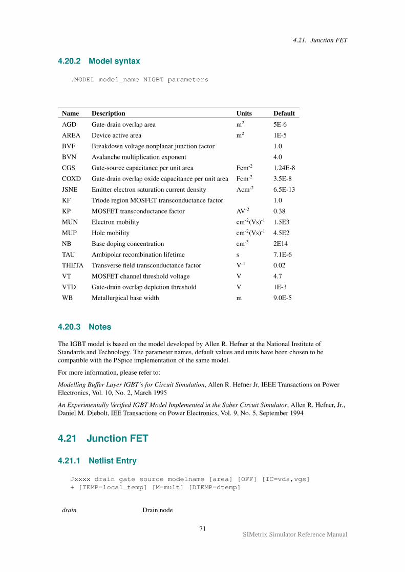
4.21. Junction FET
4.20.2 Model syntax
.MODEL model_name NIGBT parameters
Name Description Units Default
AGD Gate-drain overlap area m2 5E-6
AREA Device active area m2 1E-5
BVF Breakdown voltage nonplanar junction factor 1.0
BVN Avalanche multiplication exponent 4.0
CGS Gate-source capacitance per unit area Fcm-2 1.24E-8
COXD Gate-drain overlap oxide capacitance per unit area Fcm-2 3.5E-8
JSNE Emitter electron saturation current density Acm-2 6.5E-13
KF Triode region MOSFET transconductance factor 1.0
KP MOSFET transconductance factor AV-2 0.38
MUN Electron mobility cm-2(Vs)-1 1.5E3
MUP Hole mobility cm-2(Vs)-1 4.5E2
NB Base doping concentration cm-3 2E14
TAU Ambipolar recombination lifetime s 7.1E-6
THETA Transverse field transconductance factor V-1 0.02
VT MOSFET channel threshold voltage V 4.7
VTD Gate-drain overlap depletion threshold V 1E-3
WB Metallurgical base width m 9.0E-5
4.20.3 Notes
The IGBT model is based on the model developed by Allen R. Hefner at the National Institute ofStandards and Technology. The parameter names, default values and units have been chosen to becompatible with the PSpice implementation of the same model.
For more information, please refer to:
Modelling Buffer Layer IGBT’s for Circuit Simulation, Allen R. Hefner Jr, IEEE Transactions on PowerElectronics, Vol. 10, No. 2, March 1995
An Experimentally Verified IGBT Model Implemented in the Saber Circuit Simulator, Allen R. Hefner, Jr.,Daniel M. Diebolt, IEE Transactions on Power Electronics, Vol. 9, No. 5, September 1994
4.21 Junction FET
4.21.1 Netlist Entry
Jxxxx drain gate source modelname [area] [OFF] [IC=vds,vgs]+ [TEMP=local_temp] [M=mult] [DTEMP=dtemp]
drain Drain node
71SIMetrix Simulator Reference Manual
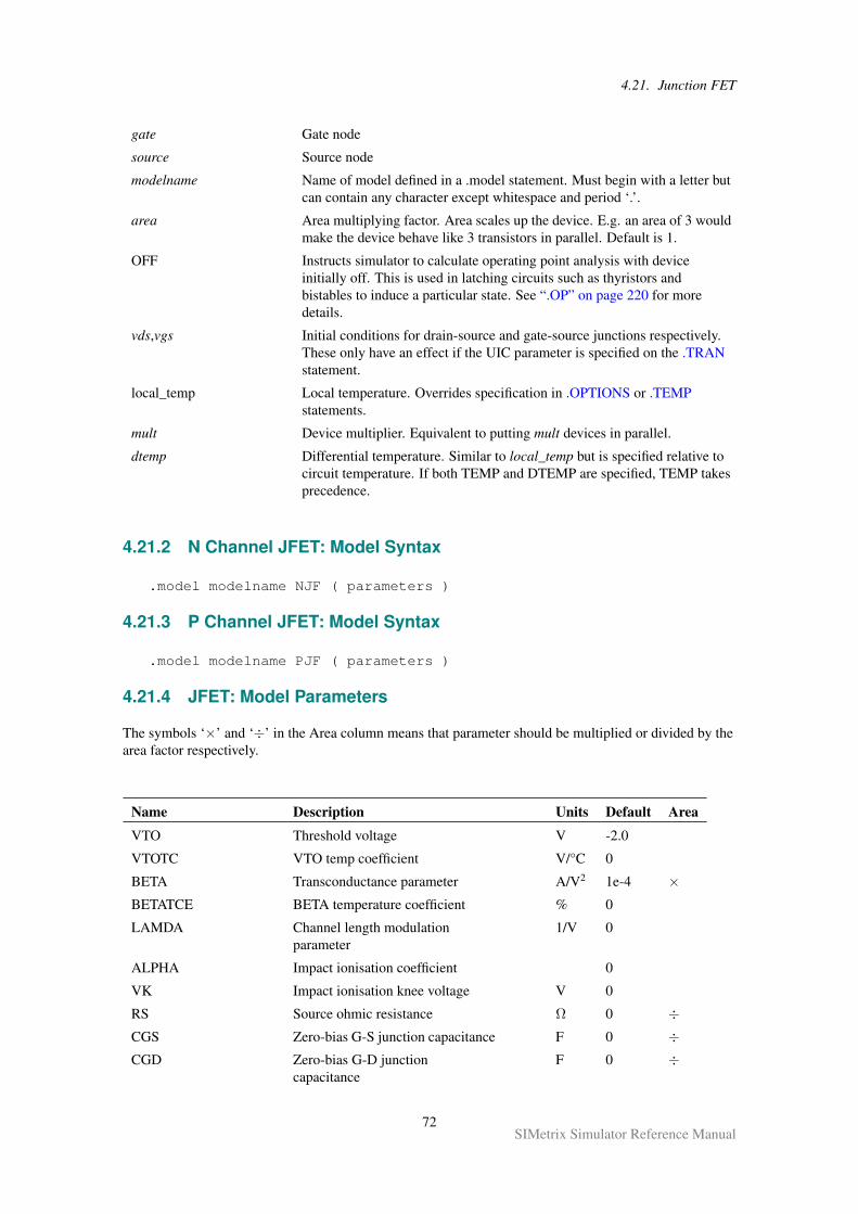
4.21. Junction FET
gate Gate node
source Source node
modelname Name of model defined in a .model statement. Must begin with a letter butcan contain any character except whitespace and period ‘.’.
area Area multiplying factor. Area scales up the device. E.g. an area of 3 wouldmake the device behave like 3 transistors in parallel. Default is 1.
OFF Instructs simulator to calculate operating point analysis with deviceinitially off. This is used in latching circuits such as thyristors andbistables to induce a particular state. See “.OP” on page 220 for moredetails.
vds,vgs Initial conditions for drain-source and gate-source junctions respectively.These only have an effect if the UIC parameter is specified on the .TRANstatement.
local_temp Local temperature. Overrides specification in .OPTIONS or .TEMPstatements.
mult Device multiplier. Equivalent to putting mult devices in parallel.
dtemp Differential temperature. Similar to local_temp but is specified relative tocircuit temperature. If both TEMP and DTEMP are specified, TEMP takesprecedence.
4.21.2 N Channel JFET: Model Syntax
.model modelname NJF ( parameters )
4.21.3 P Channel JFET: Model Syntax
.model modelname PJF ( parameters )
4.21.4 JFET: Model Parameters
The symbols ‘×’ and ‘÷’ in the Area column means that parameter should be multiplied or divided by thearea factor respectively.
Name Description Units Default Area
VTO Threshold voltage V -2.0
VTOTC VTO temp coefficient V/°C 0
BETA Transconductance parameter A/V2 1e-4 ×BETATCE BETA temperature coefficient % 0
LAMDA Channel length modulationparameter
1/V 0
ALPHA Impact ionisation coefficient 0
VK Impact ionisation knee voltage V 0
RS Source ohmic resistance Ω 0 ÷CGS Zero-bias G-S junction capacitance F 0 ÷CGD Zero-bias G-D junction
capacitanceF 0 ÷
72SIMetrix Simulator Reference Manual
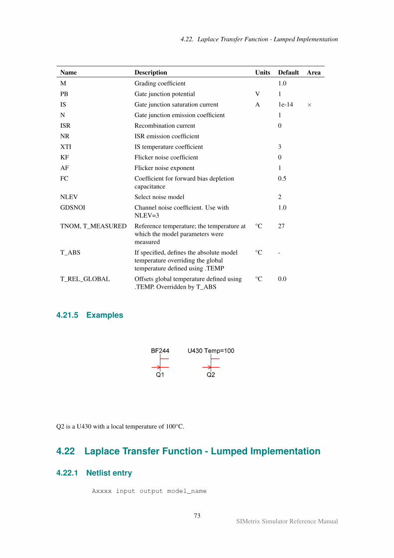
4.22. Laplace Transfer Function - Lumped Implementation
Name Description Units Default Area
M Grading coefficient 1.0
PB Gate junction potential V 1
IS Gate junction saturation current A 1e-14 ×N Gate junction emission coefficient 1
ISR Recombination current 0
NR ISR emission coefficient
XTI IS temperature coefficient 3
KF Flicker noise coefficient 0
AF Flicker noise exponent 1
FC Coefficient for forward bias depletioncapacitance
0.5
NLEV Select noise model 2
GDSNOI Channel noise coefficient. Use withNLEV=3
1.0
TNOM, T_MEASURED Reference temperature; the temperature atwhich the model parameters weremeasured
°C 27
T_ABS If specified, defines the absolute modeltemperature overriding the globaltemperature defined using .TEMP
°C -
T_REL_GLOBAL Offsets global temperature defined using.TEMP. Overridden by T_ABS
°C 0.0
4.21.5 Examples
Q2 is a U430 with a local temperature of 100°C.
4.22 Laplace Transfer Function - Lumped Implementation
4.22.1 Netlist entry
Axxxx input output model_name
73SIMetrix Simulator Reference Manual
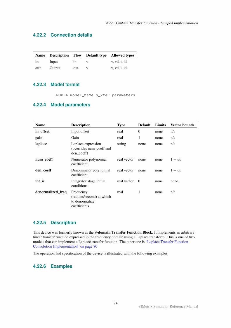
4.22. Laplace Transfer Function - Lumped Implementation
4.22.2 Connection details
Name Description Flow Default type Allowed types
in Input in v v, vd, i, id
out Output out v v, vd, i, id
4.22.3 Model format
.MODEL model_name s_xfer parameters
4.22.4 Model parameters
Name Description Type Default Limits Vector bounds
in_offset Input offset real 0 none n/a
gain Gain real 1 none n/a
laplace Laplace expression(overrides num_coeff andden_coeff)
string none none n/a
num_coeff Numerator polynomialcoefficient
real vector none none 1−∞
den_coeff Denominator polynomialcoefficient
real vector none none 1−∞
int_ic Integrator stage initialconditions
real vector 0 none none
denormalized_freq Frequency(radians/second) at whichto denormalizecoefficients
real 1 none n/a
4.22.5 Description
This device was formerly known as the S-domain Transfer Function Block. It implements an arbitrarylinear transfer function expressed in the frequency domain using a Laplace transform. This is one of twomodels that can implement a Laplace transfer function. The other one is “Laplace Transfer FunctionConvolution Implementation” on page 80
The operation and specification of the device is illustrated with the following examples.
4.22.6 Examples
74SIMetrix Simulator Reference Manual
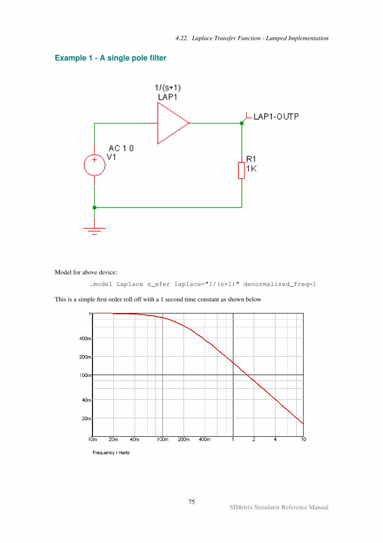
4.22. Laplace Transfer Function - Lumped Implementation
Example 1 - A single pole filter
Model for above device:
.model Laplace s_xfer laplace="1/(s+1)" denormalized_freq=1
This is a simple first order roll off with a 1 second time constant as shown below
75SIMetrix Simulator Reference Manual
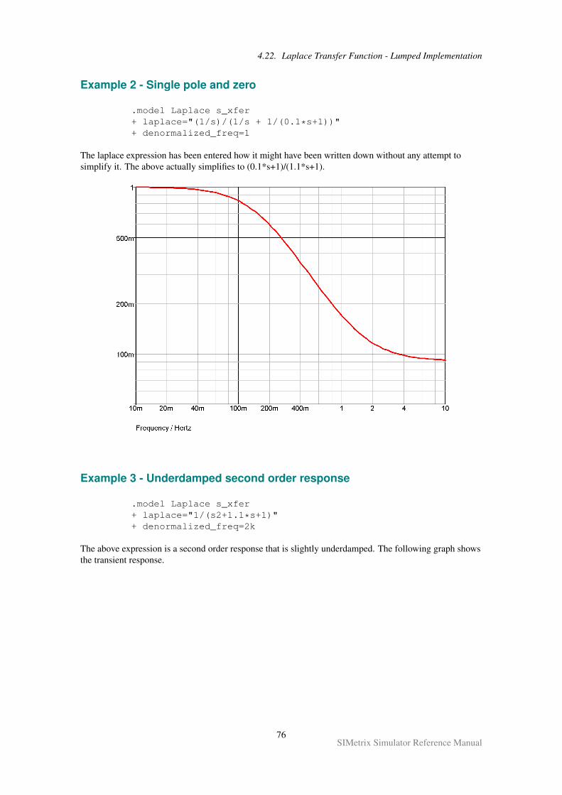
4.22. Laplace Transfer Function - Lumped Implementation
Example 2 - Single pole and zero
.model Laplace s_xfer+ laplace="(1/s)/(1/s + 1/(0.1*s+1))"+ denormalized_freq=1
The laplace expression has been entered how it might have been written down without any attempt tosimplify it. The above actually simplifies to (0.1*s+1)/(1.1*s+1).
Example 3 - Underdamped second order response
.model Laplace s_xfer+ laplace="1/(s2+1.1*s+1)"+ denormalized_freq=2k
The above expression is a second order response that is slightly underdamped. The following graph showsthe transient response.
76SIMetrix Simulator Reference Manual
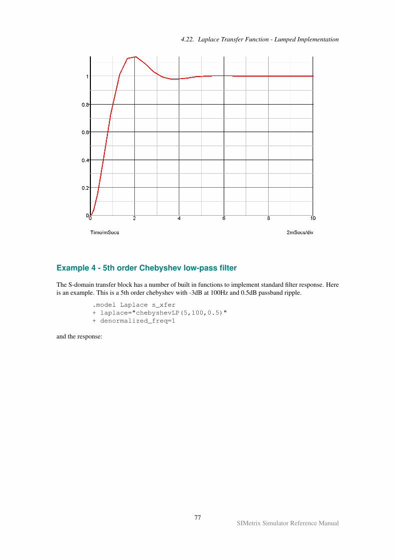
4.22. Laplace Transfer Function - Lumped Implementation
Example 4 - 5th order Chebyshev low-pass filter
The S-domain transfer block has a number of built in functions to implement standard filter response. Hereis an example. This is a 5th order chebyshev with -3dB at 100Hz and 0.5dB passband ripple.
.model Laplace s_xfer+ laplace="chebyshevLP(5,100,0.5)"+ denormalized_freq=1
and the response:
77SIMetrix Simulator Reference Manual
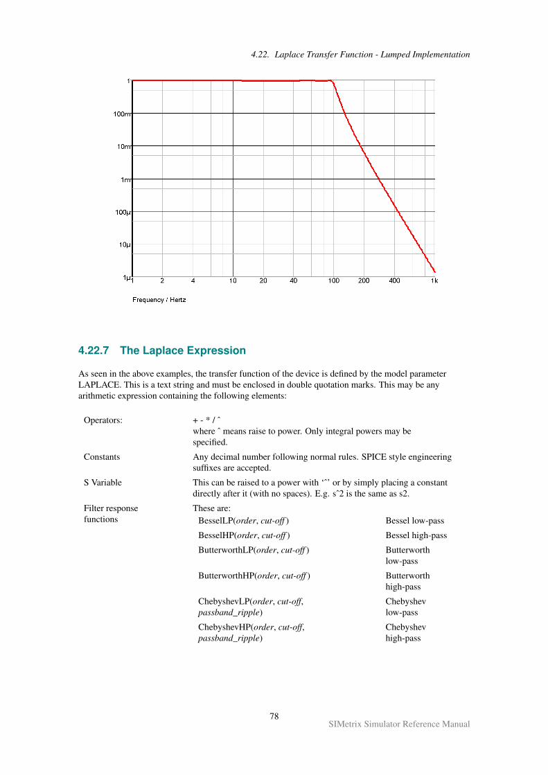
4.22. Laplace Transfer Function - Lumped Implementation
4.22.7 The Laplace Expression
As seen in the above examples, the transfer function of the device is defined by the model parameterLAPLACE. This is a text string and must be enclosed in double quotation marks. This may be anyarithmetic expression containing the following elements:
Operators: + - * / ˆwhere ˆ means raise to power. Only integral powers may bespecified.
Constants Any decimal number following normal rules. SPICE style engineeringsuffixes are accepted.
S Variable This can be raised to a power with ‘ˆ’ or by simply placing a constantdirectly after it (with no spaces). E.g. sˆ2 is the same as s2.
Filter responsefunctions
These are:BesselLP(order, cut-off ) Bessel low-pass
BesselHP(order, cut-off ) Bessel high-pass
ButterworthLP(order, cut-off ) Butterworthlow-pass
ButterworthHP(order, cut-off ) Butterworthhigh-pass
ChebyshevLP(order, cut-off,passband_ripple)
Chebyshevlow-pass
ChebyshevHP(order, cut-off,passband_ripple)
Chebyshevhigh-pass
78SIMetrix Simulator Reference Manual
4.22. Laplace Transfer Function - Lumped Implementation
Where:order Integer specifying order of filter. There is no
maximum limit but in practice orders larger thanabout 50 tend to give accuracy problems.
cut-off -3dB Frequency in Hertz
passband_ripple Chebyshev only. Passband ripple spec. in dB
4.22.8 Defining the Laplace Expression Using Coefficients
Instead of entering a Laplace expression as a string, this can also be entered as two arrays of numericcoefficients for the numerator and denominator. In general this is less convenient than entering theexpression directly, but has the benefit that it supports the use of parameters. In this method, use theNUM_COEFF and DEN_COEFF parameters instead of the LAPLACE expression.
The following simple example, demonstrates the method
.param f0=10
.param w0 = 2*3.14159265*f0
.model laplace s_xfer num_coeff = [1] den_coeff = [1/w0,1]
4.22.9 Other Model Parameters
• DENORMALISED_FREQ is a frequency scaling factor.
• INT_IC specifies the initial conditions for the device. This is an array of maximum size equal to theorder of the denominator. The right-most value is the zero’th order initial condition.
• NUM_COEFF and DEN_COEFF - see “Defining the Laplace Expression Using Coefficients” onpage 79.
• GAIN and IN_OFFSET are the DC gain and input offset respectively.
4.22.10 Limitations
SIMetrix expands the expression you enter to create a quotient of two polynomials. If the constant terms ofboth numerator and denominator are both zero, both are divided by S. That process is repeated until one orboth of the polynomials has a non-zero constant term.
The result of this process must satisfy the following:
• The order the denominator must be greater than or equal to that of the numerator.
• The constant term of the denominator may not be zero.
4.22.11 Implementation
This device implements a Laplace transform using a network of integrators. The diagram below shows theconfiguration used for a third order network.
79SIMetrix Simulator Reference Manual
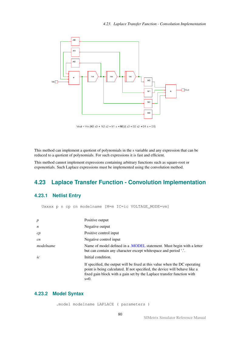
4.23. Laplace Transfer Function - Convolution Implementation
This method can implement a quotient of polynomials in the s variable and any expression that can bereduced to a quotient of polynomials. For such expressions it is fast and efficient.
This method cannot implement expressions containing arbitrary functions such as square-root orexponentials. Such Laplace expressions must be implemented using the convolution method.
4.23 Laplace Transfer Function - Convolution Implementation
4.23.1 Netlist Entry
Uxxxx p n cp cn modelname [M=m IC=ic VOLTAGE_MODE=vm]
p Positive output
n Negative output
cp Positive control input
cn Negative control input
modelname Name of model defined in a .MODEL statement. Must begin with a letterbut can contain any character except whitespace and period ‘.’.
ic Initial condition.
If specified, the output will be fixed at this value when the DC operatingpoint is being calculated. If not specified, the device will behave like afixed gain block with a gain set by the Laplace transfer function withs=0.
4.23.2 Model Syntax
.model modelname LAPLACE ( parameters )
80SIMetrix Simulator Reference Manual
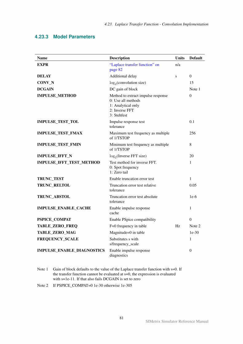
4.23. Laplace Transfer Function - Convolution Implementation
4.23.3 Model Parameters
Name Description Units Default
EXPR “Laplace transfer function” onpage 82
n/a
DELAY Additional delay s 0
CONV_N log2(convolution size) 15
DCGAIN DC gain of block Note 1
IMPULSE_METHOD Method to extract impulse response0: Use all methods1: Analytical only2: Inverse FFT3: Stehfest
0
IMPULSE_TEST_TOL Impulse response testtolerance
0.1
IMPULSE_TEST_FMAX Maximum test frequency as multipleof 1/TSTOP
256
IMPULSE_TEST_FMIN Minimum test frequency as multipleof 1/TSTOP
8
IMPULSE_IFFT_N log2(Inverse FFT size) 20
IMPULSE_IFFT_TEST_METHOD Test method for inverse FFT.0: Spot frequency1: Zero tail
1
TRUNC_TEST Enable truncation error test 1
TRUNC_RELTOL Truncation error test relativetolerance
0.05
TRUNC_ABSTOL Truncation error test absolutetolerance
1e-6
IMPULSE_ENABLE_CACHE Enable impulse responsecache
1
PSPICE_COMPAT Enable PSpice compatibility 0
TABLE_ZERO_FREQ F=0 frequency in table Hz Note 2
TABLE_ZERO_MAG Magnitude=0 in table 1e-30
FREQUENCY_SCALE Substitutes s withs/frequency_scale
1
IMPULSE_ENABLE_DIAGNOSTICS Enable impulse responsediagnostics
0
Note 1 Gain of block defaults to the value of the Laplace transfer function with s=0. Ifthe transfer function cannot be evaluated at s=0, the expression is evaluatedwith s=1e-11. If that also fails DCGAIN is set to zero
Note 2 If PSPICE_COMPAT=0 1e-30 otherwise 1e-305
81SIMetrix Simulator Reference Manual
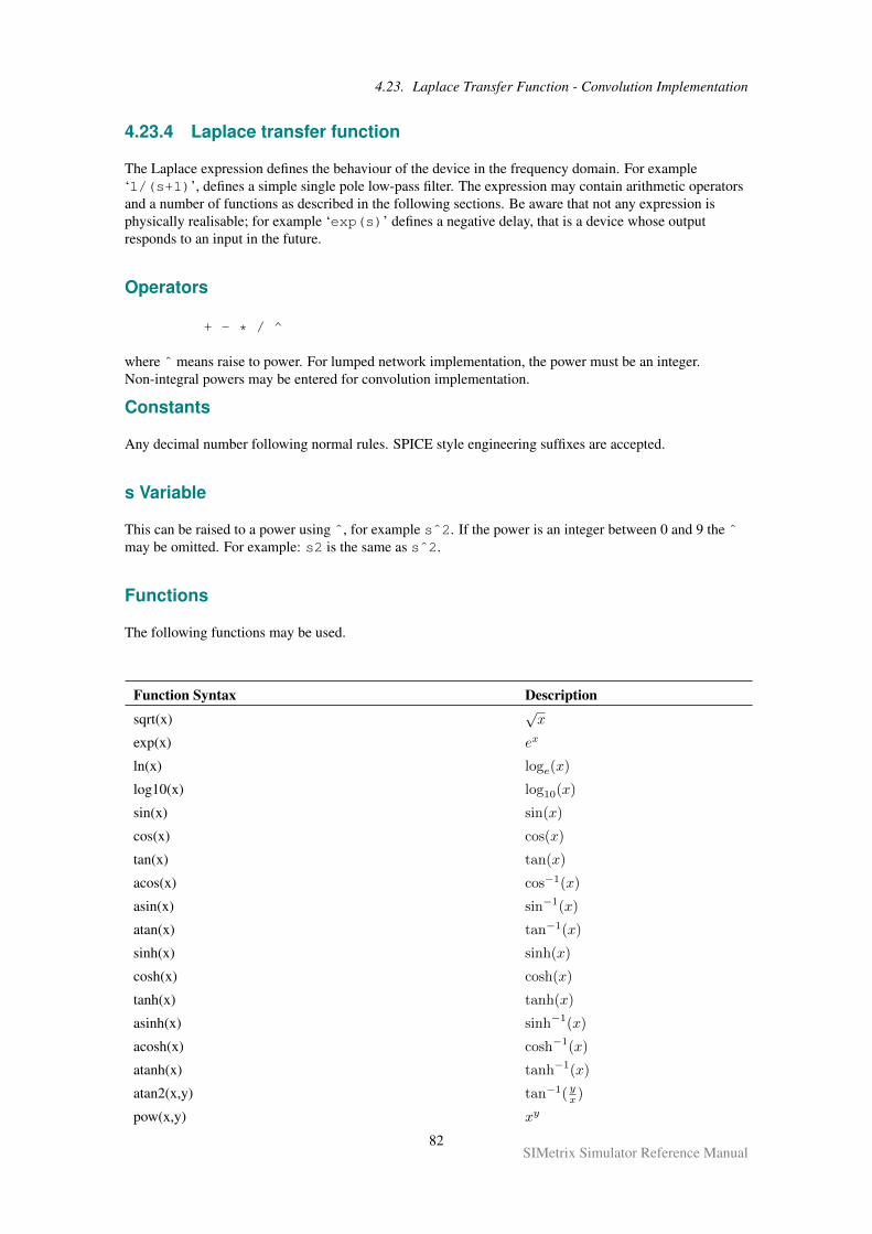
4.23. Laplace Transfer Function - Convolution Implementation
4.23.4 Laplace transfer function
The Laplace expression defines the behaviour of the device in the frequency domain. For example‘1/(s+1)’, defines a simple single pole low-pass filter. The expression may contain arithmetic operatorsand a number of functions as described in the following sections. Be aware that not any expression isphysically realisable; for example ‘exp(s)’ defines a negative delay, that is a device whose outputresponds to an input in the future.
Operators
+ - * / ^
where ˆ means raise to power. For lumped network implementation, the power must be an integer.Non-integral powers may be entered for convolution implementation.
Constants
Any decimal number following normal rules. SPICE style engineering suffixes are accepted.
s Variable
This can be raised to a power using ˆ, for example sˆ2. If the power is an integer between 0 and 9 the ˆmay be omitted. For example: s2 is the same as sˆ2.
Functions
The following functions may be used.
Function Syntax Description
sqrt(x)√x
exp(x) ex
ln(x) loge(x)
log10(x) log10(x)
sin(x) sin(x)
cos(x) cos(x)
tan(x) tan(x)
acos(x) cos−1(x)
asin(x) sin−1(x)
atan(x) tan−1(x)
sinh(x) sinh(x)
cosh(x) cosh(x)
tanh(x) tanh(x)
asinh(x) sinh−1(x)
acosh(x) cosh−1(x)
atanh(x) tanh−1(x)
atan2(x,y) tan−1( yx )
pow(x,y) xy
82SIMetrix Simulator Reference Manual
4.23. Laplace Transfer Function - Convolution Implementation
Filter response functions
Filter response functions may be used in both lumped network implementation and convolutionimplementation.
These are described in the following table:
Function Syntax Filter Response
BesselLP(order, cut-off) Bessel low-pass
BesselHP(order, cut-off) Bessel high-pass
ButterworthLP(order, cut-off) Butterworth low-pass
ButterworthHP(order, cut-off) Butterworth high-pass
ChebyshevLP(order, cut-off, passband_ripple) Chebyshev low-pass
ChebyshevHP(order, cut-off, passband_ripple) Chebyshev high-pass
Where:
order Integer specifying order of filter. There is no maximum limit but inpractice orders larger than about 50 tend to give accuracyproblems.
cut-off -3dB Frequency in Hertz.
passband_ripple Chebyshev only. Passband ripple spec. in dB.
Lookup tables
The frequency response of a system may be defined in tabular form using lookup tables. The lookup tableconsists of a sequence of values arranged in triplets. Each triplet is in the form frequency, value1, value2where value1 and value2 define the magnitude and phase in various ways as described below.
There are five variants of the lookup table as described below:
Function Name value1 value2
Table dB phase in degrees
Table_M magnitude phase in degrees
Table_R dB phase in radians
Table_MR magnitude phase in radians
Table_RI real part imaginary part
Example
Table_M(0.01,1,30, 1,1,30, 10,0.1,30, 100,0.01,-30)
The above defines a response with a gain of 1 and a phase shift of 30 degrees from 0.01Hz to 1Hz. From1Hz to 10Hz the gain falls from 1 to 0.1 with the phase shift remaining at 30 degrees. From 10Hz to100Hz the gain falls from 0.1 to 0.01 and the phase changes from 30 to -30 degrees.
In real life it is not possible to implement a characteristic with the above behaviour as it is non-causal.However, it can be implemented if a suitable delay is added to the characteristic. The delay may be added
83SIMetrix Simulator Reference Manual
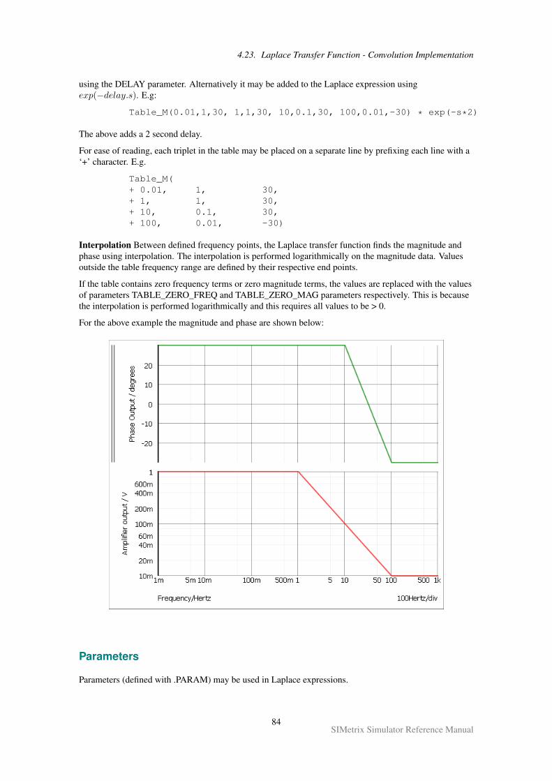
4.23. Laplace Transfer Function - Convolution Implementation
using the DELAY parameter. Alternatively it may be added to the Laplace expression usingexp(−delay.s). E.g:
Table_M(0.01,1,30, 1,1,30, 10,0.1,30, 100,0.01,-30) * exp(-s*2)
The above adds a 2 second delay.
For ease of reading, each triplet in the table may be placed on a separate line by prefixing each line with a‘+’ character. E.g.
Table_M(+ 0.01, 1, 30,+ 1, 1, 30,+ 10, 0.1, 30,+ 100, 0.01, -30)
Interpolation Between defined frequency points, the Laplace transfer function finds the magnitude andphase using interpolation. The interpolation is performed logarithmically on the magnitude data. Valuesoutside the table frequency range are defined by their respective end points.
If the table contains zero frequency terms or zero magnitude terms, the values are replaced with the valuesof parameters TABLE_ZERO_FREQ and TABLE_ZERO_MAG parameters respectively. This is becausethe interpolation is performed logarithmically and this requires all values to be > 0.
For the above example the magnitude and phase are shown below:
Parameters
Parameters (defined with .PARAM) may be used in Laplace expressions.
84SIMetrix Simulator Reference Manual
4.23. Laplace Transfer Function - Convolution Implementation
4.23.5 Implementation
The Laplace transfer function is implemented using a convolution method.
In the frequency domain, a linear system may be represented by:
V out(s) = V in(s).f(s)
where f(s) is the transfer function.
In the time domain the same system may be represented by:
V out(t) = V in(t) ∗ f(t)
Where f(t) is the impulse response of f(s) and ∗ is the convolution operator.
This method is challenging to implement as simple convolution applied to simulation data in its raw formis an O(n2) algorithm. This means that the number of computations required at each step is proportionalto the square of the number of steps. In practice this becomes unacceptably slow when there are more thanabout 10000 time steps.
SIMetrix overcomes this performance limitation by using an FFT based fast convolution method with acomputation speed of O(n log 2n). Although dramatically faster, this algorithm requires data to bepresented to it at fixed-interval steps which has the effect of placing an upper frequency limit. The actualupper frequency limit can be arbitrarily increased by increasing the number of steps (the value of n) at theexpense of speed and the memory consumed. In practice the default settings work well in mostapplications and give good performance and accuracy.
To perform the convolution, the simulator must also extract the impulse response of the Laplace transform.SIMetrix has three methods to do this:
Analytical Matches the Laplace transform to known analytical solutions.For example 1√
(s) has the impulse response of 12.π√t. SIMetrix
will automatically detect this and other known Laplacetransforms.
Inverse FFT Calculates the inverse Fourier transform of the Laplaceexpression. This is a general purpose method that can beapplied to a wide-range of Laplace transforms. However, it hasthe condition that the impulse response must decay to zeroduring the time interval.
Stehfest method A method to calculate the inverse Laplace transform.Sometimes this method works for slowly decaying transformsthat fail with the inverse FFT method.
4.23.6 Impulse Response
Problems with Impulse Response Extraction
For the convolution method an impulse response of the Laplace transfer function must be extracted. Asmentioned above, three methods are attempted. The inverse FFT method and Stehfest methods areapproximate in nature and for this reason, the result from each method is tested. If the test fails the impulseresponse is rejected and another method is attempted. If all methods fail the simulation will abort.
Transfer functions that decay slowly are likely to fail the inverse FFT method as this method requires thatthe impulse response decay to zero or nearly to zero. If the Stehfest method also fails, the problem cansometimes be resolved by increasing the inverse FFT size. This is controlled by the IMPULSE_IFFT_N
85SIMetrix Simulator Reference Manual
4.23. Laplace Transfer Function - Convolution Implementation
parameter. This increases the duration over which the inverse FFT is evaluated so providing a longer timeto decay.
In many situations the impulse response extraction fails because the transfer function is non-causal. Thismeans that it has a response in negative time. Non-causal transfer functions can be made causal by addinga delay.
Impulse Response Testing
If the inverse FFT method or Stehfest methods are used to extract the impulse response, the result is testedbefore allowing it to be used for the simulation.
The Stehfest method is tested by performing a spot frequency check. That is the impulse response is usedto measure the gain of a sequence of sine waves in the time domain to check that the magnitudes match tothat predicted in the frequency domain. The parameters IMPULSE_TEST_FMAX andIMPULSE_TEST_FMIN determine the range of frequencies used.
The inverse FFT method may be tested by one of two methods determined by theIMPULSE_IFFT_TEST_METHOD parameter. If set to 0, the spot frequency method as described abovewill be used. If set to 1, the default, the impulse response is tested by measuring its decay to zero. Theinverse FFT method is accurate if the response decays to zero and this is used to test the result.
The tolerance required for the test is set by the IMPULSE_TEST_TOL parameter.
Impulse Response Cache
The impulse response is cached to speed up subsequent simulations with the same response. The cache islocated here:
C:\Users\<login-name>\AppData\Roaming\SIMetrix Technologies\SIMetrix810\LaplaceCache
where <login-name> is the name used to log in to your system. This can be deleted at any time. The cacheis size limited to 250Mbytes by default. This can be changed using the option variableLaplaceCacheSizeMBytes. Type ‘Set LaplaceCacheSizeMBytes=nnn’ at the command line to set a newvalue.
The cache may be disabled by setting the IMPULSE_ENABLE_CACHE parameter to 0.
Impulse Response Analytical Extraction
The impulse response analytical extraction attempts to match the transfer function to one of the followingpatterns. The parameters a, b, c etc represent constant values.
Laplace expression Impulse response
a a.δ(t)
a/(b.s) a/b
a/√b.s a/
√2.π.b.t
a/(b.s+ c) a/b.e−c/b.t
a/√b.s+ c a ∗ e−c.t/b/
√b.π.t√
a/(b.s+ c)√a ∗ e−c.t/b/
√b.π.t
a
b.s2 + c.s+ d
−(e−t/2(√p2−4q+p) − et/2(
√p2−4q−p)√
p2 − 4qp = c/b and q = d/b
86SIMetrix Simulator Reference Manual
4.23. Laplace Transfer Function - Convolution Implementation
Laplace expression Impulse response
a.eb.s a.δ(b+ t)
a/(b.sc)a.tc−1
b.Γ(c)a.s2 + b.s+ c
d.s2 + g.s+ f[−(e
t.arg2−et.arg3)∗(−p.u+2q+u2−2v)2arg1 − (u−p)(et.arg2+et.arg3)
2 + δ(t)]ad
p = b/aq = c/au = g/dv = f/darg1 =
√u2 − 4v
arg2 = −arg1/2− u/2arg3 = arg1/2− u/2
a.s+ b
c.s2 + d.s+ f
a
c.(2q − u)(arg2− arg3) +
√u2 − 4v(arg3 + arg2)
2√u2 − 4v
q = b/au = d/cv = f/c
arg2 = et.(√u2−4v/2−u/2)
arg3 = et.(−√u2−4v/2−u/2)
a.s+ b
c.s+ d
e−d.t/c(b.c− a.d)
c2+a.δ(t)
c
√a.s+ b√c.s+ d
(α.(I1(α.t)− I0(α.t)) + δ(t)).e−β.t.Y
Y =√a/c
α = (d/c− b/a)/2β = (d/c+ b/a)/2I0 and I1 are Bessel functions
The analytic matching algorithm will attempt to match partial expressions as well as the whole expressionif they are combined by addition, subtraction or multiplication. For example:
(1/(s+ 1)) ∗ exp(−s)
will be matched to the product of 1/(s+ 1) and exp(−s). Respectively these have impulse responses ofe−t and δ(1 + t) and those two impulse responses will be convolved to yield the final result. Note that thisonly succeeds if all partial expressions can be matched analytically.
To exploit this method, ensure that the expression is entered in a manner that keeps each partial expressiondistinct. For example, the following would be matched correctly:
1/(s+ 1) ∗ 1/(s+ 2)
as this would be seen as the two partial expressions 1/(s+ 1) and 1/(s+ 2) each of which can be resolvedanalytically. The final result would be obtained by convolving the two impulse responses.
However the following mathematically identical expression would not be matched:
1/((s+ 1) ∗ (s+ 2))
The analysis algorithm does not attempt to decompose denominator products so this will not be recognisedanalytically. The above would be extracted using inverse FFT which would usually be successful but
87SIMetrix Simulator Reference Manual
4.24. Lossy Transmission Line
might not be if the run time is considerably shorter than the time constant.
4.23.7 Run Time Error Control
During the simulation run the time step is controlled using a truncation error method. The tolerances usedfor this error control are set using the TRUNC_RELTOL and TRUNC_ABSTOL parameters. Thetruncation error test may be disabled altogether by setting the TRUNC_TEST parameter to zero.
4.23.8 PSpice LAPLACE and FREQ compatibility
SIMetrix is compatible with PSpice Laplace transfer functions at the netlist level entered in one of theseforms
Exxx n1 n2 LAPLACE input_expression laplace_expression Gxxx n1 n2 LAPLACE input_expression laplace_expression
Exxx n1 n2 FREQ input_expression [keyword1] [keyword2] table_values DELAY=delayGxxx n1 n2 FREQ input_expression [keyword1] [keyword2] table_values DELAY=delay
Where:
input_expression Expression to define input signal. E.g. V(vin)
laplace_expression Laplace transfer function
keyword1 and keyword2 RAD, MAG, DB, DEG or R_I
table_values table look up entries in groups of three
delay additional delay
SIMetrix will implement the PSpice expression in the best way possible. If the Laplace expression can beexpressed as a quotient of polynomials, the lumped model (see “Laplace Transfer Function - LumpedImplementation” on page 73) will be used instead of the convolution model as long as it does not containany parameters.
4.24 Lossy Transmission Line
4.24.1 Netlist Entry
Oxxxx p1 n1 p2 n2 modelname [IC=v1,i1,v2,i2]
p1 Positive input port 1
n1 Negative input port 1
p2 Positive input port 2
n2 Negative input port 2
modelname Name of model defined in a .MODEL statement. Must begin with a letterbut can contain any character except whitespace and period ‘.’.
v1,i1,v2,i2 Initial conditions for voltage at port 1, current at port 1, voltage at port 2and current at port 2 respectively. These only have an effect if the UICparameter is specified on the .TRAN statement.
88SIMetrix Simulator Reference Manual
4.24. Lossy Transmission Line
4.24.2 Model Syntax
.model modelname LTRA ( parameters )
4.24.3 Model Parameters
Name Description Units Default
R Resistance/unit length Ω/unit length 0.0
L Inductance/unit length Henrys/unit length 0.0
G Conductance/unit length Siemens(mhos)/unit length 0.0
C Capacitance/unit length Farads/unit length 0.0
LEN Length Required
REL Relative rate of change of derivative forbreakpoint
1.0
ABS Absolute rate of change of derivative forbreakpoint
1.0
The parameters REL and ABS control the way the line is simulated rather than its electrical characteristics.More accurate results (at the expense of simulation time) can be obtained by using lower values.
Notes
The uniform RLC/RC/LC/RG transmission line model (LTRA) models a uniform constant-parameterdistributed transmission line. The LC case may also be modelled using the lossless transmission linemodel. The operation of the lossy transmission line model is based on the convolution of the transmissionline’s impulse responses with its inputs.
The following types of lines have been implemented:
RLC Transmission line with series loss only
RC Uniform RC line
LC Lossless line
RG Distributed series resistance and parallel conductance
All other combinations will lead to an error.
REL and ABS are model parameters that control the setting of breakpoints. A breakpoint is a point in timewhen an analysis is unconditionally performed. The more there are the more accurate the result but thelonger it will take to arrive. Reducing REL and/or ABS will yield greater precision.
89SIMetrix Simulator Reference Manual
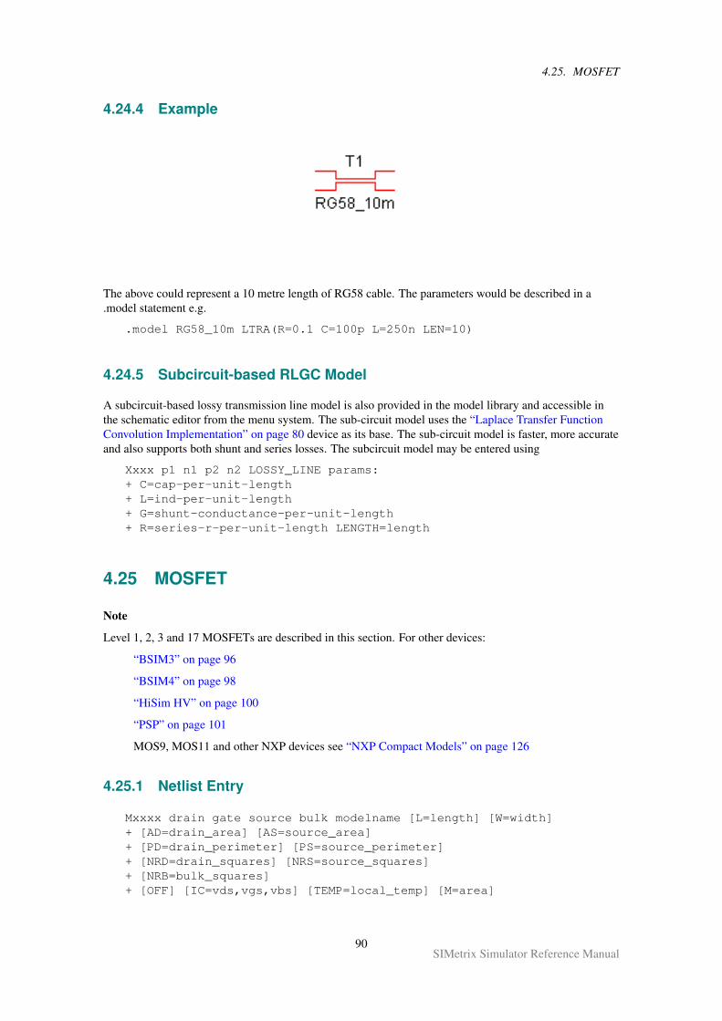
4.25. MOSFET
4.24.4 Example
The above could represent a 10 metre length of RG58 cable. The parameters would be described in a.model statement e.g.
.model RG58_10m LTRA(R=0.1 C=100p L=250n LEN=10)
4.24.5 Subcircuit-based RLGC Model
A subcircuit-based lossy transmission line model is also provided in the model library and accessible inthe schematic editor from the menu system. The sub-circuit model uses the “Laplace Transfer FunctionConvolution Implementation” on page 80 device as its base. The sub-circuit model is faster, more accurateand also supports both shunt and series losses. The subcircuit model may be entered using
Xxxx p1 n1 p2 n2 LOSSY_LINE params:+ C=cap-per-unit-length+ L=ind-per-unit-length+ G=shunt-conductance-per-unit-length+ R=series-r-per-unit-length LENGTH=length
4.25 MOSFET
Note
Level 1, 2, 3 and 17 MOSFETs are described in this section. For other devices:
“BSIM3” on page 96
“BSIM4” on page 98
“HiSim HV” on page 100
“PSP” on page 101
MOS9, MOS11 and other NXP devices see “NXP Compact Models” on page 126
4.25.1 Netlist Entry
Mxxxx drain gate source bulk modelname [L=length] [W=width]+ [AD=drain_area] [AS=source_area]+ [PD=drain_perimeter] [PS=source_perimeter]+ [NRD=drain_squares] [NRS=source_squares]+ [NRB=bulk_squares]+ [OFF] [IC=vds,vgs,vbs] [TEMP=local_temp] [M=area]
90SIMetrix Simulator Reference Manual
4.25. MOSFET
drain Drain node
gate Gate node
source Source node
bulk Bulk (substrate) node
modelname Name of model. Must begin with a letter but can contain any characterexcept whitespace and period ‘.’
(The following 8 parameters are not supported by the level 17 MOSFET model)
length Channel length (metres).
width Channel width (metres).
drain_area Drain area (m2).
source_area Source area (m2).
drain_perimeter Drain perimeter (metres).
source_perimeter Source perimeter (metres).
drain_squares Equivalent number of squares for drain resistance
source_squares Equivalent number of squares for source resistance
gate_squares Equivalent number of squares for gate resistance. Level=3 only
bulk_squares Equivalent number of squares for gate resistance. Level=3 only
OFF Instructs simulator to calculate operating point analysis with deviceinitially off. This is used in latching circuits such as thyristors andbistables to induce a particular state. See “.OP” on page 220 for moredetails.
vds, vgs, vbs Initial condition voltages for drain-source gate-source andbulk(=substrate)-source respectively. These only have an effect if the UICparameter is specified on the .TRAN statement.
local_temp Local temperature. Overrides specification in .OPTIONS or .TEMPstatements.
dtemp Differential temperature. Similar to local_temp but is specified relative tocircuit temperature. If both TEMP and DTEMP are specified, TEMP takesprecedence. Currently implemented only for LEVEL 1,2 and 3.
Notes SIMetrix supports four types of MOSFET model specified in the model definition.These are referred to as levels 1, 2, 3 and 7. Levels 1,2, and 3 are the same as theSPICE2 and SPICE3 equivalents. Level 17 is proprietary to SIMetrix. For furtherinformation see Level 17 MOSFET parameters below.
4.25.2 NMOS Model Syntax
.model modelname NMOS ( level=level_number parameters )
4.25.3 PMOS Model Syntax
.model modelname PMOS ( level=level_number parameters )
4.25.4 MOS Levels 1, 2 and 3: Model Parameters
91SIMetrix Simulator Reference Manual
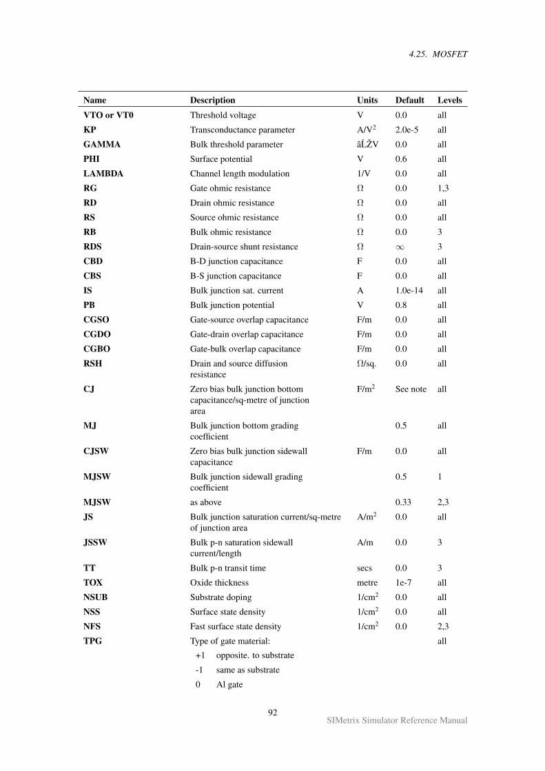
4.25. MOSFET
Name Description Units Default Levels
VTO or VT0 Threshold voltage V 0.0 all
KP Transconductance parameter A/V2 2.0e-5 all
GAMMA Bulk threshold parameter âLŽV 0.0 all
PHI Surface potential V 0.6 all
LAMBDA Channel length modulation 1/V 0.0 all
RG Gate ohmic resistance Ω 0.0 1,3
RD Drain ohmic resistance Ω 0.0 all
RS Source ohmic resistance Ω 0.0 all
RB Bulk ohmic resistance Ω 0.0 3
RDS Drain-source shunt resistance Ω ∞ 3
CBD B-D junction capacitance F 0.0 all
CBS B-S junction capacitance F 0.0 all
IS Bulk junction sat. current A 1.0e-14 all
PB Bulk junction potential V 0.8 all
CGSO Gate-source overlap capacitance F/m 0.0 all
CGDO Gate-drain overlap capacitance F/m 0.0 all
CGBO Gate-bulk overlap capacitance F/m 0.0 all
RSH Drain and source diffusionresistance
Ω/sq. 0.0 all
CJ Zero bias bulk junction bottomcapacitance/sq-metre of junctionarea
F/m2 See note all
MJ Bulk junction bottom gradingcoefficient
0.5 all
CJSW Zero bias bulk junction sidewallcapacitance
F/m 0.0 all
MJSW Bulk junction sidewall gradingcoefficient
0.5 1
MJSW as above 0.33 2,3
JS Bulk junction saturation current/sq-metreof junction area
A/m2 0.0 all
JSSW Bulk p-n saturation sidewallcurrent/length
A/m 0.0 3
TT Bulk p-n transit time secs 0.0 3
TOX Oxide thickness metre 1e-7 all
NSUB Substrate doping 1/cm2 0.0 all
NSS Surface state density 1/cm2 0.0 all
NFS Fast surface state density 1/cm2 0.0 2,3
TPG Type of gate material:
+1 opposite. to substrate
-1 same as substrate
0 Al gate
all
92SIMetrix Simulator Reference Manual
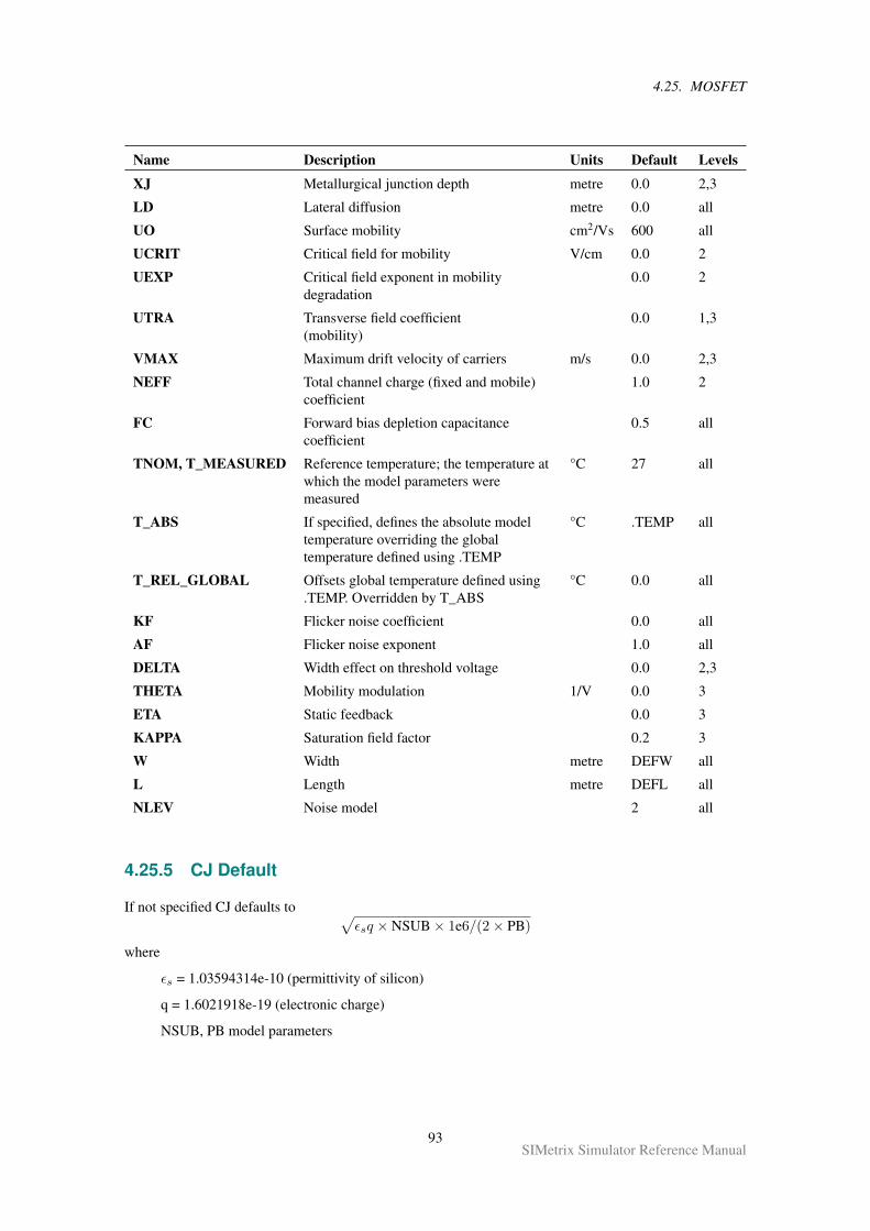
4.25. MOSFET
Name Description Units Default Levels
XJ Metallurgical junction depth metre 0.0 2,3
LD Lateral diffusion metre 0.0 all
UO Surface mobility cm2/Vs 600 all
UCRIT Critical field for mobility V/cm 0.0 2
UEXP Critical field exponent in mobilitydegradation
0.0 2
UTRA Transverse field coefficient(mobility)
0.0 1,3
VMAX Maximum drift velocity of carriers m/s 0.0 2,3
NEFF Total channel charge (fixed and mobile)coefficient
1.0 2
FC Forward bias depletion capacitancecoefficient
0.5 all
TNOM, T_MEASURED Reference temperature; the temperature atwhich the model parameters weremeasured
°C 27 all
T_ABS If specified, defines the absolute modeltemperature overriding the globaltemperature defined using .TEMP
°C .TEMP all
T_REL_GLOBAL Offsets global temperature defined using.TEMP. Overridden by T_ABS
°C 0.0 all
KF Flicker noise coefficient 0.0 all
AF Flicker noise exponent 1.0 all
DELTA Width effect on threshold voltage 0.0 2,3
THETA Mobility modulation 1/V 0.0 3
ETA Static feedback 0.0 3
KAPPA Saturation field factor 0.2 3
W Width metre DEFW all
L Length metre DEFL all
NLEV Noise model 2 all
4.25.5 CJ Default
If not specified CJ defaults to √εsq × NSUB× 1e6/(2× PB)
where
εs = 1.03594314e-10 (permittivity of silicon)
q = 1.6021918e-19 (electronic charge)
NSUB, PB model parameters
93SIMetrix Simulator Reference Manual
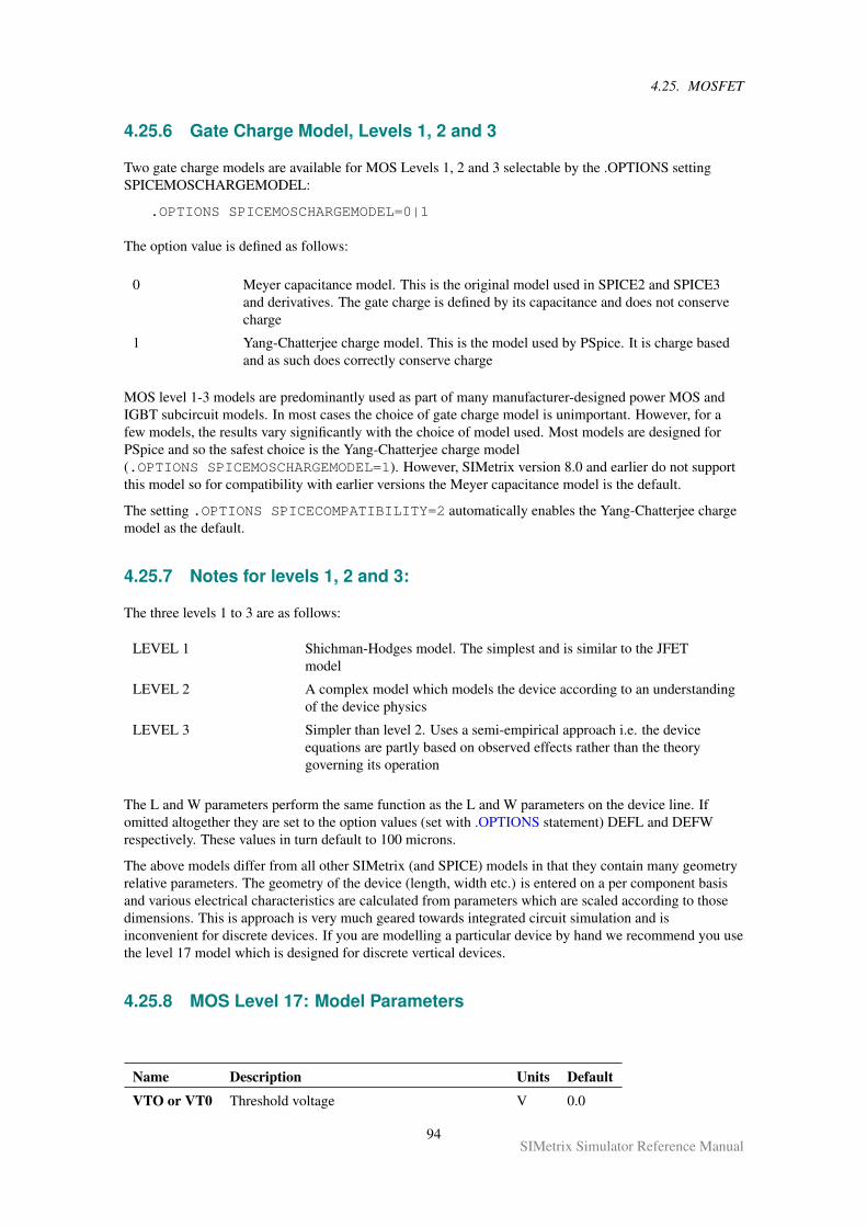
4.25. MOSFET
4.25.6 Gate Charge Model, Levels 1, 2 and 3
Two gate charge models are available for MOS Levels 1, 2 and 3 selectable by the .OPTIONS settingSPICEMOSCHARGEMODEL:
.OPTIONS SPICEMOSCHARGEMODEL=0|1
The option value is defined as follows:
0 Meyer capacitance model. This is the original model used in SPICE2 and SPICE3and derivatives. The gate charge is defined by its capacitance and does not conservecharge
1 Yang-Chatterjee charge model. This is the model used by PSpice. It is charge basedand as such does correctly conserve charge
MOS level 1-3 models are predominantly used as part of many manufacturer-designed power MOS andIGBT subcircuit models. In most cases the choice of gate charge model is unimportant. However, for afew models, the results vary significantly with the choice of model used. Most models are designed forPSpice and so the safest choice is the Yang-Chatterjee charge model(.OPTIONS SPICEMOSCHARGEMODEL=1). However, SIMetrix version 8.0 and earlier do not supportthis model so for compatibility with earlier versions the Meyer capacitance model is the default.
The setting .OPTIONS SPICECOMPATIBILITY=2 automatically enables the Yang-Chatterjee chargemodel as the default.
4.25.7 Notes for levels 1, 2 and 3:
The three levels 1 to 3 are as follows:
LEVEL 1 Shichman-Hodges model. The simplest and is similar to the JFETmodel
LEVEL 2 A complex model which models the device according to an understandingof the device physics
LEVEL 3 Simpler than level 2. Uses a semi-empirical approach i.e. the deviceequations are partly based on observed effects rather than the theorygoverning its operation
The L and W parameters perform the same function as the L and W parameters on the device line. Ifomitted altogether they are set to the option values (set with .OPTIONS statement) DEFL and DEFWrespectively. These values in turn default to 100 microns.
The above models differ from all other SIMetrix (and SPICE) models in that they contain many geometryrelative parameters. The geometry of the device (length, width etc.) is entered on a per component basisand various electrical characteristics are calculated from parameters which are scaled according to thosedimensions. This is approach is very much geared towards integrated circuit simulation and isinconvenient for discrete devices. If you are modelling a particular device by hand we recommend you usethe level 17 model which is designed for discrete vertical devices.
4.25.8 MOS Level 17: Model Parameters
Name Description Units Default
VTO or VT0 Threshold voltage V 0.0
94SIMetrix Simulator Reference Manual
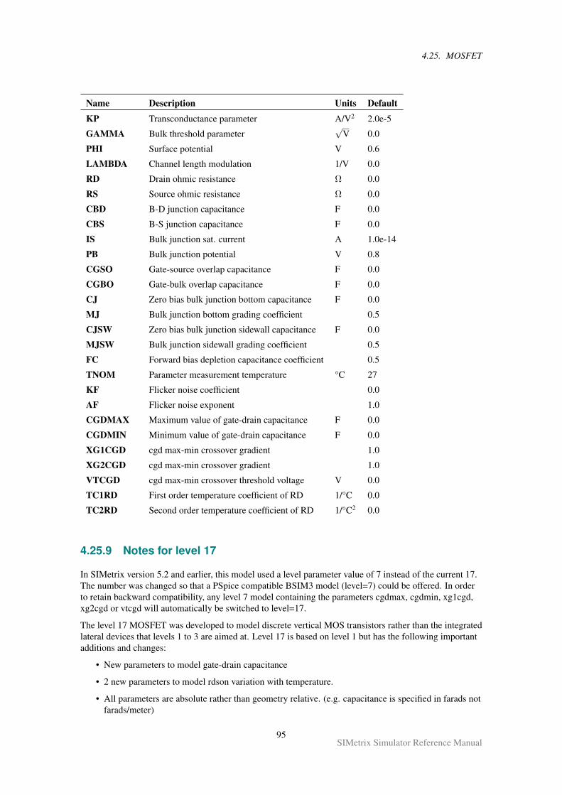
4.25. MOSFET
Name Description Units Default
KP Transconductance parameter A/V2 2.0e-5
GAMMA Bulk threshold parameter√
V 0.0
PHI Surface potential V 0.6
LAMBDA Channel length modulation 1/V 0.0
RD Drain ohmic resistance Ω 0.0
RS Source ohmic resistance Ω 0.0
CBD B-D junction capacitance F 0.0
CBS B-S junction capacitance F 0.0
IS Bulk junction sat. current A 1.0e-14
PB Bulk junction potential V 0.8
CGSO Gate-source overlap capacitance F 0.0
CGBO Gate-bulk overlap capacitance F 0.0
CJ Zero bias bulk junction bottom capacitance F 0.0
MJ Bulk junction bottom grading coefficient 0.5
CJSW Zero bias bulk junction sidewall capacitance F 0.0
MJSW Bulk junction sidewall grading coefficient 0.5
FC Forward bias depletion capacitance coefficient 0.5
TNOM Parameter measurement temperature °C 27
KF Flicker noise coefficient 0.0
AF Flicker noise exponent 1.0
CGDMAX Maximum value of gate-drain capacitance F 0.0
CGDMIN Minimum value of gate-drain capacitance F 0.0
XG1CGD cgd max-min crossover gradient 1.0
XG2CGD cgd max-min crossover gradient 1.0
VTCGD cgd max-min crossover threshold voltage V 0.0
TC1RD First order temperature coefficient of RD 1/°C 0.0
TC2RD Second order temperature coefficient of RD 1/°C2 0.0
4.25.9 Notes for level 17
In SIMetrix version 5.2 and earlier, this model used a level parameter value of 7 instead of the current 17.The number was changed so that a PSpice compatible BSIM3 model (level=7) could be offered. In orderto retain backward compatibility, any level 7 model containing the parameters cgdmax, cgdmin, xg1cgd,xg2cgd or vtcgd will automatically be switched to level=17.
The level 17 MOSFET was developed to model discrete vertical MOS transistors rather than the integratedlateral devices that levels 1 to 3 are aimed at. Level 17 is based on level 1 but has the following importantadditions and changes:
• New parameters to model gate-drain capacitance
• 2 new parameters to model rdson variation with temperature.
• All parameters are absolute rather than geometry relative. (e.g. capacitance is specified in farads notfarads/meter)
95SIMetrix Simulator Reference Manual
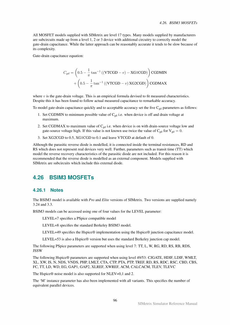
4.26. BSIM3 MOSFETs
All MOSFET models supplied with SIMetrix are level 17 types. Many models supplied by manufacturersare subcircuits made up from a level 1, 2 or 3 device with additional circuitry to correctly model thegate-drain capacitance. While the latter approach can be reasonably accurate it tends to be slow because ofits complexity.
Gate-drain capacitance equation:
Cgd =
(0.5− 1
πtan−1 ((VTCGD− v)− XG1CGD)
)CGDMIN
+
(0.5− 1
πtan−1 ((VTCGD− v) XG2CGD)
)CGDMAX
where v is the gate-drain voltage. This is an empirical formula devised to fit measured characteristics.Despite this it has been found to follow actual measured capacitance to remarkable accuracy.
To model gate-drain capacitance quickly and to acceptable accuracy set the five Cgd parameters as follows:
1. Set CGDMIN to minimum possible value of Cgd i.e. when device is off and drain voltage atmaximum.
2. Set CGDMAX to maximum value of Cgd i.e. when device is on with drain-source voltage low andgate-source voltage high. If this value is not known use twice the value of Cgd for Vgd = 0.
3. Set XG2CGD to 0.5, XG1CGD to 0.1 and leave VTCGD at default of 0.
Although the parasitic reverse diode is modelled, it is connected inside the terminal resistances, RD andRS which does not represent real devices very well. Further, parameters such as transit time (TT) whichmodel the reverse recovery characteristics of the parasitic diode are not included. For this reason it isrecommended that the reverse diode is modelled as an external component. Models supplied withSIMetrix are subcircuits which include this external diode.
4.26 BSIM3 MOSFETs
4.26.1 Notes
The BSIM3 model is available with Pro and Elite versions of SIMetrix. Two versions are supplied namely3.24 and 3.3.
BSIM3 models can be accessed using one of four values for the LEVEL parameter:
LEVEL=7 specifies a PSpice compatible model
LEVEL=8 specifies the standard Berkeley BSIM3 model.
LEVEL=49 specifies the Hspice® implementation using the Hspice® junction capacitance model.
LEVEL=53 is also a Hspice® version but uses the standard Berkeley junction cap model.
The following PSpice parameters are supported when using level 7: TT, L, W, RG, RD, RS, RB, RDS,JSSW
The following Hspice® parameters are supported when using level 49/53: CJGATE, HDIF, LDIF, WMLT,XL, XW, IS, N, NDS, VNDS, PHP, LMLT, CTA, CTP, PTA, PTP, TREF, RD, RS, RDC, RSC, CBD, CBS,FC, TT, LD, WD, EG, GAP1, GAP2, XLREF, XWREF, ACM, CALCACM, TLEV, TLEVC
The Hspice® noise model is also supported for NLEV=0,1 and 2.
The ‘M’ instance parameter has also been implemented with all variants. This specifies the number ofequivalent parallel devices.
96SIMetrix Simulator Reference Manual
4.26. BSIM3 MOSFETs
Additional temperature parameters: All variants support the TEMP and DTEMP instance parameters.TEMP specifies absolute temperature (Celsius) while DTEMP specifies the temperature relative to thecircuit global temperature.
All variants support the model parameters T_MEASURED (equivalent to TNOM), T_ABS (as TEMPinstance parameter) and T_REL_GLOBAL (as DTEMP instance parameter)
4.26.2 Version Selector
The VERSION parameter can be specified to select which version is used. As detailed above, SIMetrixsupports three different BSIM3 versions although 8 versions have been released by Berkeley. Thefollowing table shows which version will actually be used according to the VERSION parameter value.
VERSION parameter Use BSIM3 Version
3.2 3.24
3.21 3.24
3.22 3.24
3.23 3.24
3.24 3.24
3.3 3.3
not specified 3.3
Note that a second decimal point will be ignored so 3.2.4 is the same as 3.24. If the version parameter isset to a value not listed above, SIMetrix will raise an error condition. This can be overridden by setting.OPTIONS AnyVersion.
4.26.3 Model Parameters
The parameters describing BSIM3 are documented in the original Berkeley manual. See below. Thefollowing table lists parameters that are non-standard.
Name Description Units Default
TNOM, T_MEASURED Reference temperature; the temperature atwhich the model parameters weremeasured
°C 27
T_ABS If specified, defines the absolute modeltemperature overriding the global temperaturedefined using .TEMP
°C .TEMP
T_REL_GLOBAL Offsets global temperature defined using.TEMP. Overridden by T_ABS
°C 0.0
VFBFLAG Capacitor model selector used by Hspice. Anerror will be raised if this parameter and theCAPMOD parameter are set to values notsupported by SIMetrix
0
BINFLAG Parameter used by Hspice. An error will beraised if this parameter is set to a value otherthan zero
0
97SIMetrix Simulator Reference Manual
4.27. BSIM4 MOSFETs
Name Description Units Default
LREF Ignored
WREF Ignored
SFVTFLAG Ignored
TT Level = 7 only. Reverse diode transittime
S 0.0
L Level = 7 only. Channel length. Overridden byinstance parameter
m DEFL option
W Level = 7 only. Channel width. Overridden byinstance parameter
m DEFW option
RG Level = 7 only. Gate resistance W 0.0
RD Level = 7 only. Drain resistance W 0.0
RS Level = 7 only. Source resistance W 0.0
RB Level = 7 only. Bulk resistance W 0.0
RDS Level = 7 only. Drain-source leakageresistance
W ∞
JSSW Level = 7 only. Alias for JSW. F/m 0.0
4.26.4 Further Documentation
Original Berkeley documentation is provided on the CDROM and at our web site. Please visit “FurtherDocumentation” on page 98 for details.
4.26.5 Process Binning
BSIM3 devices may be binned according to length and width. Refer to “Model Binning” on page 32 fordetails.
4.27 BSIM4 MOSFETs
4.27.1 Notes
The BSIM4 model is only available with the Elite versions of SIMetrix.
BSIM4 models are accessed using LEVEL=14.
Versions 4.21, 4.3, 4.4, 4.5, 4.60, 4.61, 4.62, 4.63, 4.64, 4.65 and 4.70 are currently supported. To set theversion to be used, use the VERSION parameter as defined in the following table:
VERSION parameter Use BSIM4 version
4.0 4.21
4.1 4.21
4.2 4.21
4.21 4.21
98SIMetrix Simulator Reference Manual
4.27. BSIM4 MOSFETs
VERSION parameter Use BSIM4 version
4.3 4.3
4.4 4.4
4.5 4.5
4.6 4.6
4.61 4.61
4.62 4.62
4.63 4.63
4.64 4.64
4.65 4.65
4.70 4.70
Omitted 4.70
Other See notes
Note that a second decimal point will be ignored so 4.2.1 is the same as 4.21. If the version parameter isset to a value not listed above, SIMetrix will raise an error condition. This can be overridden by setting.OPTIONS AnyVersion.
The implementation is standard Berkeley but with the addition of the ‘M’ instance parameter whichspecifies the number of equivalent parallel devices.
4.27.2 Further Documentation
Original Berkeley documentation is provided on the CDROM and at our web site. Please visit “FurtherDocumentation” on page 99 for details. Note the document covers version 4.70 of the model. Earlierversions are available from the BSIM3/4 web site at BSIM Reference.
4.27.3 Process Binning
BSIM4 devices may be binned according to length and width. Refer to “Model Binning” on page 32 fordetails. Note the multi-fingered devices are binned according to width per finger.
4.27.4 Mapping to Level 54 for Hspice
Hspice uses Level 54 to define BSIM4 MOSFETs whereas the SIMetrix level is 14. TheHSPICEMODELS option setting may be used to change this:
.OPTIONS HSPICEMODELS=1
This setting also has the same effect:
.OPTIONS HSPICECOMPATIBILITY=1
See “.OPTIONS” on page 222 for more details
99SIMetrix Simulator Reference Manual
4.28. HiSim HV MOSFET
4.28 HiSim HV MOSFET
4.28.1 Notes
The HiSim HV model is accessed as LEVEL=62 and is available with the Elite versions of SIMetrix. Thedevice may have up to 6 terminals and the netlist format is as follows:
Mxxx drain gate source bulk [ substrate [ temperature ]]modelname instance_parameters
The substrate and temperature nodes are internally connected to ground if they are omitted. Currently wehave no information about whether this is the expected behaviour.
Most mainstream models that we implement, such as BSIM3 and BSIM4, we alter to clean up the variouserror and warning messages that they emit. In particular we make the appropriate changes to ensure themessages are displayed in the list file. This is a time consuming task and generally has to be repeated fornew versions. We have not done this work for this model and so most of the warning and error messagesare as the original designers provided and are directed to “stdout” or “stderr”. This means that you will notsee them when using SIMetrix via the GUI unless you specifically enable a feature that directs thesimulator’s stdout and stderr output to the front end. This can be done by typing the following at thecommand line:
Set EnableSimStdoutSet EnableSimStderr
If running the simulator in ‘console’ mode, the stdout and stderr messages will be displayed in the consolewithout needing any special configuration.
This model may be binned on length and width in a similar manner to the BSIM3 model. See “ModelBinning” on page 32.
4.29 MOSFET GMIN Implementation
GMIN is a conductance added to all non-linear devices to improve DC convergence. For LEVEL 1-3 andLEVEL 17 MOSFETs, the default GMIN is implemented as shown below:
This is compatible with SPICE and earlier versions of SIMetrix.
For BSIM3 and BSIM4 devices, and also for LEVEL1-3 and LEVEL 17 devices if the NEWGMIN.OPTIONS setting is set, the GMIN implementation is:
100SIMetrix Simulator Reference Manual
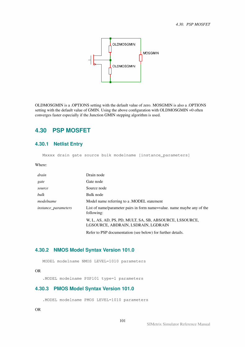
4.30. PSP MOSFET
OLDMOSGMIN is a .OPTIONS setting with the default value of zero. MOSGMIN is also a .OPTIONSsetting with the default value of GMIN. Using the above configuration with OLDMOSGMIN =0 oftenconverges faster especially if the Junction GMIN stepping algorithm is used.
4.30 PSP MOSFET
4.30.1 Netlist Entry
Mxxxx drain gate source bulk modelname [instance_parameters]
Where:
drain Drain node
gate Gate node
source Source node
bulk Bulk node
modelname Model name referring to a .MODEL statement
instance_parameters List of name/parameter pairs in form name=value. name maybe any of thefollowing:
W, L, AS, AD, PS, PD, MULT, SA, SB, ABSOURCE, LSSOURCE,LGSOURCE, ABDRAIN, LSDRAIN, LGDRAIN
Refer to PSP documentation (see below) for further details.
4.30.2 NMOS Model Syntax Version 101.0
MODEL modelname NMOS LEVEL=1010 parameters
OR
.MODEL modelname PSP101 type=1 parameters
4.30.3 PMOS Model Syntax Version 101.0
.MODEL modelname PMOS LEVEL=1010 parameters
OR
101SIMetrix Simulator Reference Manual
4.31. Resistor
.MODEL modelname PSP101 type=-1 parameters
4.30.4 NMOS Model Syntax Version 102.3
MODEL modelname NMOS LEVEL=1023 parameters
OR
.MODEL modelname PSP102 type=1 parameters
4.30.5 PMOS Model Syntax Version 102.3
.MODEL modelname PMOS LEVEL=1023 parameters
OR
.MODEL modelname PSP102 type=-1 parameters
Refer to PSP documentation (see below) for details of parameters
4.30.6 Notes
This is a model jointly developed by NXP (formerly Philips Semiconductor) and Pennsylvania StateUniversity.
Two versions are provided:
1. 101.0, non-binning, non-NQS geometric version.
2. 102.3, non-binning, non-NQS geometric version.
The model was implemented from the Verilog-A description.
Other versions of the PSP model are available from the NXP SIMKIT devices. See “SIMKIT Devices” onpage 127.
Documentation for the model is supplied on the install CDROM and at our web site. Please refer to“Further Documentation” on page 38 for details.
4.31 Resistor
4.31.1 Netlist Entry
Rxxxx n1 n2 [model_name] [value] [L=length] [W=width] [ACRES=ac_resistance][TEMP=local_temp] [TC1=tc1] [TC2=tc2] [M=mult] [DTEMP=dtemp]
n1 Node 1
n2 Node 2
model_name (Optional) Name of model. Must begin with a letter but can contain anycharacter except whitespace and ‘.’
value Resistance (W)
length Length of resistive element in metres. Only used if value is omitted. Seenotes below
width Width of resistive element in metres. Only used if value is omitted. Seenotes below
102SIMetrix Simulator Reference Manual
4.31. Resistor
ac_resistance Resistance used for AC analyses and for the calculation of thermal noise.If omitted, value defaults to final resistance value.
local_temp Resistor temperature (ËŽC)
tc1 First order temperature coefficient
tc2 Second order temperature coefficient
mult Device multiplier. Equivalent to putting mult devices in parallel.
dtemp Differential temperature. Similar to local_temp but is specified relative tocircuit temperature. If both TEMP and DTEMP are specified, TEMP takesprecedence.
4.31.2 Notes
• If model_name is omitted, value must be specified.
• If model_name is present and value is omitted, length and width must be specified in which case thevalue of the resistance is RES * RSH * L/W where RSH is the sheet resistance model parameter andRES is the resistance multiplier. See model parameters below. If ACRES is specified and non-zeroits value will be used unconditionally for AC analyses and the calculation of thermal noise.
4.31.3 Resistor Model Syntax
.model modelname R ( parameters )
4.31.4 Resistor Model Parameters
Name Description Units Default
RES Resistance multiplier 1
TC1 First order temperature coefficient 1/°C 0
TC2 Second order temperaturecoefficient
1/°C2 0
RSH Sheet resistance W/sq 0
KF Flicker noise coefficient m2/W2 0
EF Flicker noise exponent 1
TNOM, T_MEASURED Reference temperature; the temperature atwhich the model parameters weremeasured
°C 27
T_ABS If specified, defines the absolute modeltemperature overriding the globaltemperature defined using .TEMP
°C .TEMP
T_REL_GLOBAL Offsets global temperature defined using.TEMP. Overridden by T_ABS
°C 0.0
103SIMetrix Simulator Reference Manual
4.32. Resistor - Hspice Compatible
4.31.5 Notes
The flicker noise parameters are proprietary to SIMetrix. Flicker noise voltage is:
V 2n = KF · RSH2/(L ·W ) · V 2
r ·∆f/fEF
Where:
V r = Voltage across resistor.
The equation has been formulated so that KF is constant for a given resistive material.
If one of L, W is not specified, the flicker noise voltage becomes:
V 2n = KF · R2 · V 2
r ·∆f/fEF
Where R is the final resistance.
i.e. the noise current is independent of resistance. This doesn’t have any particular basis in physical lawsand is implemented this way simply for convenience. When resistor dimensions and resistivity areunavailable, the value of KF will need to be extracted for each individual value.
4.32 Resistor - Hspice Compatible
4.32.1 Netlist Entry
Rxxxx n1 n2 [model_name] [value] [L=length] [W=width] [AC=ac_resistance] [TC1=tc1][TC2=tc2] [M=mult] [SCALE=scale] [DTEMP=dtemp] [C=c]
model_name Name of .MODEL. This is compulsory unless this model made the defaultresistor. See “Making the Hspice Resistor the Default” onpage 108.
value Value of resistor. This may be an expression relating parameters definedusing .PARAM and circuit variables in the form V(n1,n2) and I(device).Expressions must be enclosed in curly braces or quotation marks.Typically the expression relates to the resistor’s own terminals in order todefine voltage dependence
length Length in metres
width Width in metres
ac_resistance Value of resistor for AC analyses. Like the main value, this may also be anexpression. See above under value for details
tc1 First order temperature coefficient
tc2 Second order temperature coefficient
mult Device multiplier. Equivalent to putting mult devices in parallel, but notethat this value does not have to be integral
scale Scales resistance and capacitance values. E.g. Reff=scale*R
dtemp Differential temperature. Device temperature = global temperature +dtemp
c Capacitance to reference node
104SIMetrix Simulator Reference Manual
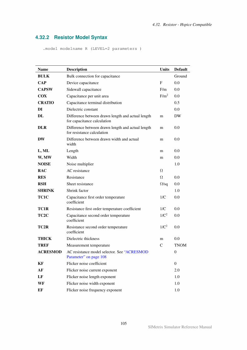
4.32. Resistor - Hspice Compatible
4.32.2 Resistor Model Syntax
.model modelname R (LEVEL=2 parameters )
Name Description Units Default
BULK Bulk connection for capacitance Ground
CAP Device capacitance F 0.0
CAPSW Sidewall capacitance F/m 0.0
COX Capacitance per unit area F/m2 0.0
CRATIO Capacitance terminal distribution 0.5
DI Dielectric constant 0.0
DL Difference between drawn length and actual lengthfor capacitance calculation
m DW
DLR Difference between drawn length and actual lengthfor resistance calculation
m 0.0
DW Difference between drawn width and actualwidth
m 0.0
L, ML Length m 0.0
W, MW Width m 0.0
NOISE Noise multiplier 1.0
RAC AC resistance WRES Resistance W 0.0
RSH Sheet resistance W/sq 0.0
SHRINK Shrink factor 1.0
TC1C Capacitance first order temperaturecoefficient
1/C 0.0
TC1R Resistance first order temperature coefficient 1/C 0.0
TC2C Capacitance second order temperaturecoefficient
1/C2 0.0
TC2R Resistance second order temperaturecoefficient
1/C2 0.0
THICK Dielectric thickness m 0.0
TREF Measurement temperature C TNOM
ACRESMOD AC resistance model selector. See “ACRESMODParameter” on page 108
0
KF Flicker noise coefficient 0
AF Flicker noise current exponent 2.0
LF Flicker noise length exponent 1.0
WF Flicker noise width exponent 1.0
EF Flicker noise frequency exponent 1.0
105SIMetrix Simulator Reference Manual
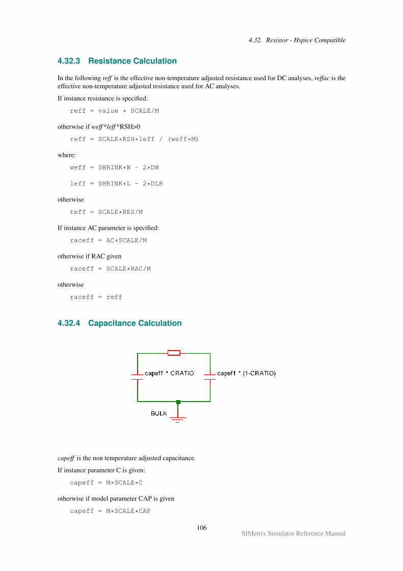
4.32. Resistor - Hspice Compatible
4.32.3 Resistance Calculation
In the following reff is the effective non-temperature adjusted resistance used for DC analyses, reffac is theeffective non-temperature adjusted resistance used for AC analyses.
If instance resistance is specified:
reff = value * SCALE/M
otherwise if weff *leff *RSH>0
reff = SCALE*RSH*leff / (weff*M)
where:
weff = SHRINK*W - 2*DW
leff = SHRINK*L - 2*DLR
otherwise
reff = SCALE*RES/M
If instance AC parameter is specified:
raceff = AC*SCALE/M
otherwise if RAC given
raceff = SCALE*RAC/M
otherwise
raceff = reff
4.32.4 Capacitance Calculation
capeff is the non temperature adjusted capacitance.
If instance parameter C is given:
capeff = M*SCALE*C
otherwise if model parameter CAP is given
capeff = M*SCALE*CAP
106SIMetrix Simulator Reference Manual
4.32. Resistor - Hspice Compatible
otherwise
capeff = (leffc*weffc*coxmod + 2*((leffc+weffc)*CAPSW))*M*SCALE
where:
leffc = SHRINK*L - 2*DL
weffc = SHRINK*W - 2*DW
See below for coxmod calculation.
Calculation of COX
If COX given
coxmod = COX
otherwise if THICK <> 0 AND DI<>0
coxmod = 8.8542149e-012*DI/THICK
otherwise if THICK <> 0 AND DI=0
coxmod = 3.453148e-011/THICK
otherwise
coxmod = 0.0
4.32.5 Temperature Scaling
Resistance
R(t) = reff * tscale
where:
tscale = 1+(tc1inst+tdelta*tc2inst)*tdelta
where
tdelta = tinst-TREF-273.15
tc1inst = if instance TC1 given: TC1 else TC1R
tc2inst = if instance TC2 given: TC2 else TC2R
tinst = [global circuit temperature] + DTEMP (Kelvin)
Capacitance
C(t) = capeff * tscale
where
tcscale = 1+(TC1C+tdelta*TC2C)*tdelta
107SIMetrix Simulator Reference Manual
4.33. CMC Resistor
tdelta defined above.
4.32.6 Flicker Noise
In =KF× IAF
LLFeff ×WWF
eff × fEF
4.32.7 ACRESMOD Parameter
This parameter controls the calculation of resistance in AC analysis. With ACRESMOD=0 AC analysisuses the large signal resistance value, that is the value of resistance calculated during the DC analysis. IfACRESMOD=1, the small signal resistance is used, that is, the value of dv/di at the operating point. If theresistance is defined as an expression containing circuit variables (i.e. it is voltage dependent), the largesignal resistance is different to the small signal resistance.
This resistor model has been developed primarily for compatibility with Hspice models. Hspice itselfalways uses the large signal resistance. However, this will create a discrepancy between AC analysis and atransient analysis of a small signal. To resolve this discrepancy, set ACRESMOD to 1.
In summary, to be compatible with Hspice, use ACRESMOD=0, for consistent results between AC andtransient analyses, use ACRESMOD=1.
In noise analysis the large signal value is always used.
4.32.8 Making the Hspice Resistor the Default
This resistor model requires the specification of a model name and the creation of a .MODEL statementwith LEVEL=2. This is likely to be inconvenient if a model file containing Hspice resistors is being used.
To overcome this, the HSPICEMODELS option setting may be used to make this resistor the default. Addthis line to the netlist:
.OPTIONS HSPICEMODELS=1
This setting also has the same effect:
.OPTIONS HSPICECOMPATIBILITY=1
See “.OPTIONS” on page 222 for more details
4.33 CMC Resistor
4.33.1 Netlist entry
Uxxxx n1 nc n2 model_name parameters
4.33.2 Model Format
.MODEL model_name R3_CMC model_parameters
Full details of this model can be found in the document r3_cmc_release1.0.0_2007Jun12.pdf which may befound on the CDROM and at our web site. Please refer to “Further Documentation” on page 38 for details.
4.34 Subcircuit Instance
108SIMetrix Simulator Reference Manual
4.35. Transmission Line
4.34.1 Netlist Entry
Xxxxx n1 n2 n3 ... subcircuit_name [pinnames: pin1 pin2 pin3 ...] [[params:][M=m] expression1 expression2 ....]
n1, n2 etc. Subcircuit nodes
pin1, pin2 etc. If the pinnames: keyword is included the names following it will be usedto name subcircuit current vectors generated by the simulator.
subcircuit_name Subcircuit name referred to in subcircuit definition (i.e. with .SUBCKTstatement)
m Multiplier. If present, the subcircuit will be multiplied by m as if therewere m devices in parallel. m may be an expression in which case it mustbe enclosed by curly braces: ‘’, ‘’.
Note that the multiplication is performed by scaling the internal devicesnot by actually replicating the subcircuit. Non integral values of m are thuspermitted. Some types of device can not currently be scaled andsubcircuits containing them will not support M. An error will displayed inthis case.
M will be interpreted as a regular parameter and will not scale thesubcircuit instance if M is declared as a parameter in the .SUBCKT line orthe following option setting is included in the netlist: .OPTIONSDisableSubcktMultiplier
expression1 etc. Parameter expressions. See “Using Expressions” on page 17.
See “Subcircuits” on page 29 for more information.
4.35 Transmission Line
4.35.1 Netlist Entry
Txxxx p1 n1 p2 n2 Z0=impedance [TD=delay] [F=frequency [NL=norm_length]][rel=rel] [abs=abs]
p1 Positive input port 1
n1 Negative input port 2
p2 Positive input port 1
n2 Negative input port 2
impedance characteristic impedance
delay Line delay (Seconds)
frequency Alternative means of specifying delay = norm_length/frequency
norm_length See frequency. Default 0.25 if omitted.
TD takes precedence over NL/F. Either TD or F must be specified.
These remaining parameters control the way the line is simulated rather than its electrical characteristics.More accurate results (at the expense of simulation time) can be obtained by using lower values.
rel Relative rate of change of derivative for breakpoint
109SIMetrix Simulator Reference Manual
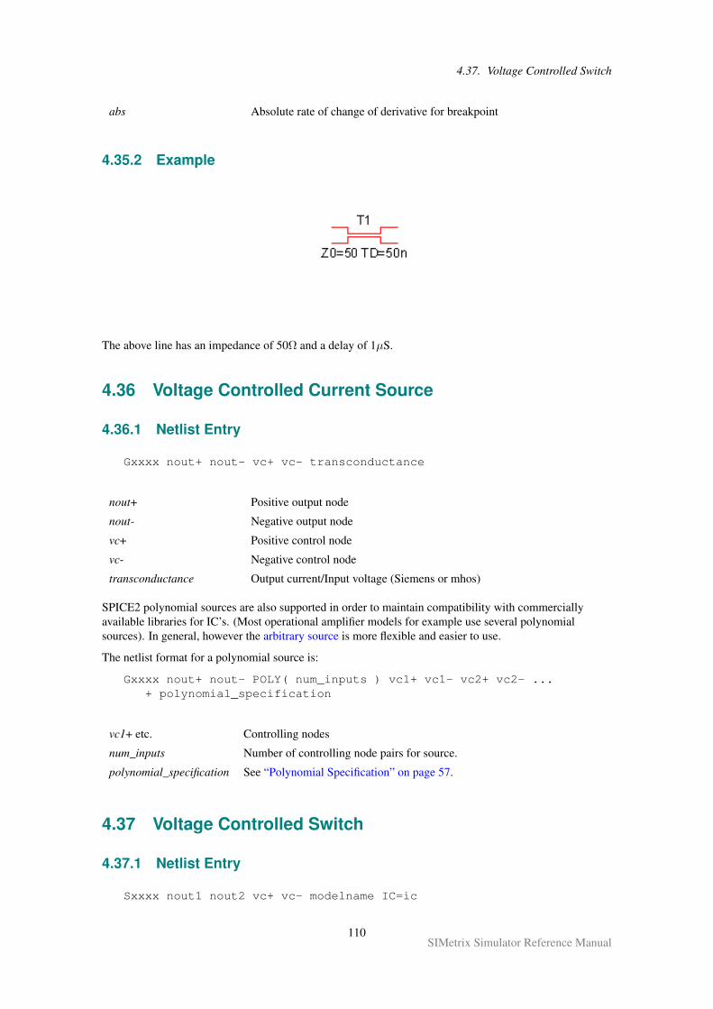
4.37. Voltage Controlled Switch
abs Absolute rate of change of derivative for breakpoint
4.35.2 Example
The above line has an impedance of 50Ω and a delay of 1µS.
4.36 Voltage Controlled Current Source
4.36.1 Netlist Entry
Gxxxx nout+ nout- vc+ vc- transconductance
nout+ Positive output node
nout- Negative output node
vc+ Positive control node
vc- Negative control node
transconductance Output current/Input voltage (Siemens or mhos)
SPICE2 polynomial sources are also supported in order to maintain compatibility with commerciallyavailable libraries for IC’s. (Most operational amplifier models for example use several polynomialsources). In general, however the arbitrary source is more flexible and easier to use.
The netlist format for a polynomial source is:
Gxxxx nout+ nout- POLY( num_inputs ) vc1+ vc1- vc2+ vc2- ...+ polynomial_specification
vc1+ etc. Controlling nodes
num_inputs Number of controlling node pairs for source.
polynomial_specification See “Polynomial Specification” on page 57.
4.37 Voltage Controlled Switch
4.37.1 Netlist Entry
Sxxxx nout1 nout2 vc+ vc- modelname IC=ic
110SIMetrix Simulator Reference Manual
4.37. Voltage Controlled Switch
nout1 Switch node 1
nout2 Switch node 2
vc+ Positive control node
vc- Negative control node
modelname Name of model. Must begin with a letter but can contain any characterexcept whitespace and period ‘.’.
ic Initial condition. Hysteresis mode only. Defines initial state of switch ifcontrol voltage is between upper and lower thresholds. 0 for ‘OFF’ 1 for‘ON’
4.37.2 Voltage Controlled Switch Model Syntax
.model modelname VSWITCH ( parameters )
OR
.model modelname SW ( parameters )
4.37.3 Voltage Controlled Switch Model Parameters
Name Description Units Default
RON On resistance Ω 1
ROFF Off resistance Ω Hysteresis mode: 1.0E12.Continuous mode: 1.0E6
VON Voltage at which switch begins to turn on.(continuous mode)
V 1
VOFF Voltage at which switch begins to turn off.(continuous mode)
V 0
VT If present enables hysteresis mode. Setsthreshold voltage
V 0.5
VH Hysteresis voltage. (hysteresis mode) V 1.0
TON On time. (hysteresis mode) s 1ns
TOFF Off time. (hysteresis mode) s 1n
TD Delay time. (hysteresis mode) s 0
TD_ON On delay. (hysteresis mode) s TD
TD_OFF Off delay. (hysteresis mode) s TD
TIMETOL Time tolerance. (hysteresis mode) s 10p
4.37.4 Voltage Controlled Switch Notes
The voltage controlled switch has two modes of operation:
1. Continuous mode: Behaves like a voltage controlled resistor. Between VON and VOFF theresistance varies gradually following a cubic law as described with the following equation:
where:
111SIMetrix Simulator Reference Manual
4.38. Voltage Controlled Source
R = 1/exp(−Lm− Lr ∗ factor ∗ (1.5− 2 ∗ factor ∗ factor))
factor = Vcontrol − 0.5
Lm = −0.5 ∗ ln(gon ∗ goff )
Lr = ln(goff/gon)
goff = ROFF <> 0 : 1/ROFF,ROFF = 0 : GMIN
gon = RON <> 0 : 1/RON,RON = 0 : GMIN
2. Hysteresis mode: Switches in a controlled time with a hysteresis characteristic. This mode isenabled if the VT parameter is defined. The switch transitions to the on state when:
Vcontrol > V T + V H
and to the off state when:
Vcontrol < V T − V H
The transition will be delayed by TD and the transition time will be TON when changing from OFFstate to ON state and TOFF when changing from ON state to OFF state.
The transition will follow the same characteristic as continuous mode. That is, during the transitionperiod the actual resistance of the switch will follow the continuous mode characteristic with thecontrol voltage following a linear transition between VON and VOFF.
Hysteresis mode is similar and usually compatible with what is known as short-transition mode inPSpice. The difference is that in short-transition mode, the switching time is uncontrolled whereasin SIMetrix hysteresis mode the transition time is controlled by the TON and TOFF parameters.
GMIN is a simulation parameter which defaults to 10E-12 but which can changed using the .OPTIONSstatement.
The SIMetrix voltage controlled switch is compatible with PSpice® but note that in hysteresis mode, theSIMetrix switches in a controlled time whereas the PSpice version switches abruptly.
4.38 Voltage Controlled Voltage Source
4.38.1 Netlist Entry
Exxxx nout+ nout- vc+ vc- gain
nout+ Positive output node
nout- Negative output node
vc+ Positive control node
vc- Negative control node
gain Output voltage/Input voltage
SPICE2 polynomial sources are also supported in order to maintain compatibility with commerciallyavailable libraries for ICs. (Most opamp models for example use several polynomial sources). In general,however the arbitrary source is more flexible and easier to use.
The netlist format for a polynomial source is:
Exxxx nout+ nout- POLY( num_inputs ) vc1+ vc1- vc2+ vc2-... polynomial_specification
112SIMetrix Simulator Reference Manual
4.39. Voltage Source
vc1+ etc. Controlling nodes
num_inputs Number of controlling node pairs for source.
polynomial_specification See “Polynomial Specification” on page 57
4.39 Voltage Source
4.39.1 Netlist Entry
Vxxxx n+ n- [[DC] dcvalue] [DCOP] [INFCAP] [AC magnitude [phase]][transient_spec]
N+ Positive node
N- Negative node
DCOP If this is specified, the voltage source will only be active during the DCoperating point solution. In other analyses, it will behave like an opencircuit. This is an effective method of creating a ‘hard’ initial condition.See “Alternative Initial Condition Implementations” on page 205 for anexample.
INFCAP If specified, the voltage source will behave as an infinite capacitor. Duringthe DC operating point solution it will behave like an open circuit. In thesubsequent analysis, it will behave like a voltage source with a value equalto the solution found during the operating point. Note that the device isinactive for DC sweeps - as all capacitors are.
dcvalue Value of source for dc operating point analysis
magnitude AC magnitude for AC sweep analysis.
phase phase for AC sweep analysis
transient_spec Specification for time varying source as described in the followingtable.
Type Description
PULSE Pulse source. Also generates, ramps, sawtooths and triangles
PWL Piece wise linear source. Can create any waveform
PWLFILE As PWL but get definition from a file
SIN Sine wave
“EXP” on page 117 Exponential signal
“SFFM” on page 118 Single frequency FM
“NOISE” on page 118 Real time noise source
4.39.2 Pulse Source
PULSE ( v1 v2 [td [tr [tf [pw [per ]]]]] )
Where:
113SIMetrix Simulator Reference Manual
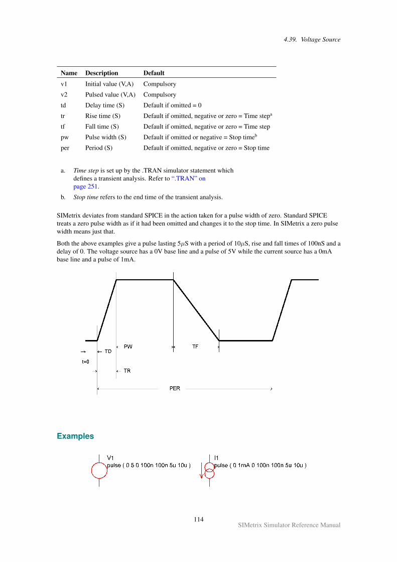
4.39. Voltage Source
Name Description Default
v1 Initial value (V,A) Compulsory
v2 Pulsed value (V,A) Compulsory
td Delay time (S) Default if omitted = 0
tr Rise time (S) Default if omitted, negative or zero = Time stepa
tf Fall time (S) Default if omitted, negative or zero = Time step
pw Pulse width (S) Default if omitted or negative = Stop timeb
per Period (S) Default if omitted, negative or zero = Stop time
a. Time step is set up by the .TRAN simulator statement whichdefines a transient analysis. Refer to “.TRAN” onpage 251.
b. Stop time refers to the end time of the transient analysis.
SIMetrix deviates from standard SPICE in the action taken for a pulse width of zero. Standard SPICEtreats a zero pulse width as if it had been omitted and changes it to the stop time. In SIMetrix a zero pulsewidth means just that.
Both the above examples give a pulse lasting 5µS with a period of 10µS, rise and fall times of 100nS and adelay of 0. The voltage source has a 0V base line and a pulse of 5V while the current source has a 0mAbase line and a pulse of 1mA.
Examples
114SIMetrix Simulator Reference Manual
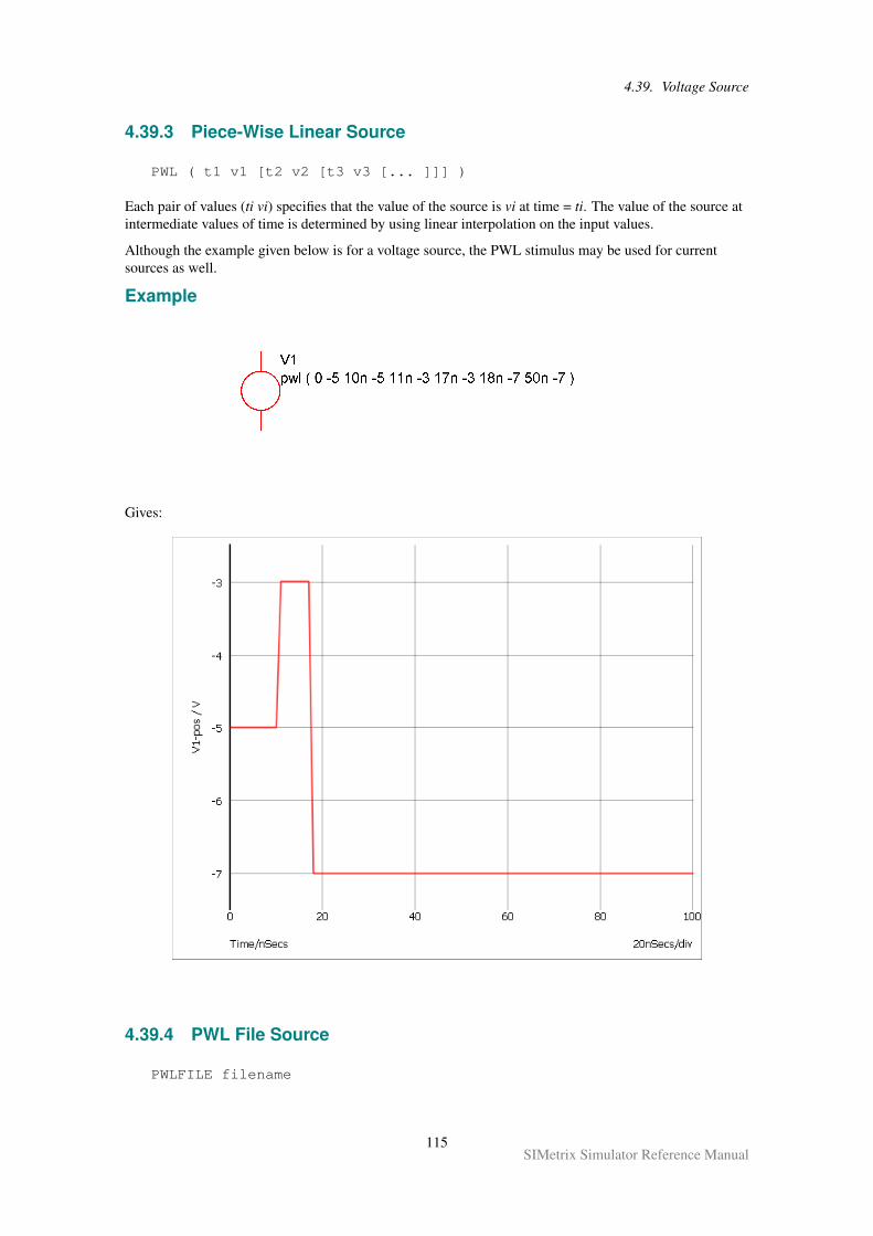
4.39. Voltage Source
4.39.3 Piece-Wise Linear Source
PWL ( t1 v1 [t2 v2 [t3 v3 [... ]]] )
Each pair of values (ti vi) specifies that the value of the source is vi at time = ti. The value of the source atintermediate values of time is determined by using linear interpolation on the input values.
Although the example given below is for a voltage source, the PWL stimulus may be used for currentsources as well.
Example
Gives:
4.39.4 PWL File Source
PWLFILE filename
115SIMetrix Simulator Reference Manual
4.39. Voltage Source
This performs the same function as the normal piece wise linear source except that the values are readfrom a file named filename.
The file contains a list of time voltage pairs in text form separated by any whitespace character (space, tab,new line). It is not necessary to add the ‘+’ continuation character for new lines but they will be ignored ifthey are included. Any non-numeric data contained in the file will also be ignored.
Notes
The PWLFILE source is considerably more efficient at reading large PWL definitions than the standardPWL source. Consequently it is recommended that all PWL definitions with more than 200 points aredefined in this way.
The data output by Show /file is directly compatible with the PWLFILE source making it possible tosave the output of one simulation and use it as a stimulus for another. It is recommended, however, that theresults are first interpolated to evenly spaced points using the Interp() function.
The use of engineering suffixes (e.g. k, m, p etc.) is not supported by PWLFILE.
The PWLFILE source is a feature of SIMetrix and does not form part of standard SPICE.
Note, you can use the simulator statements .FILE and .ENDF to define the contents of the file. E.g.
Vpwl1 N1 N2 PWLFILE pwlSource....FILE pwlSource.......ENDF
This will be read in much more efficiently than the standard PWL and is recommended for largedefinitions. See “.FILE and .ENDF” on page 197.
4.39.5 Sinusoidal Source
SIN[E] ( vo va [freq [delay [theta [ phase]]]] )
Where:
Name Description Default
vo Offset (V,A) Compulsory
va Peak (V,A) Compulsory
freq Frequency (Hz) Default if omitted or zero= 1/Stop timea
delay Delay (seconds) Default if omitted = 0
theta Damping factor (1/seconds) Default if omitted = 0
phase Phase in degrees Default if omitted = 0
a. Stop time refers to the end time of the transient analysis.
The shape of the waveform is described by:
0 to delay: vo
delay to Stop time vo+ va · e−(t−delay)..theta · sin(2π(freq · (t− delay) + phase/360))
116SIMetrix Simulator Reference Manual
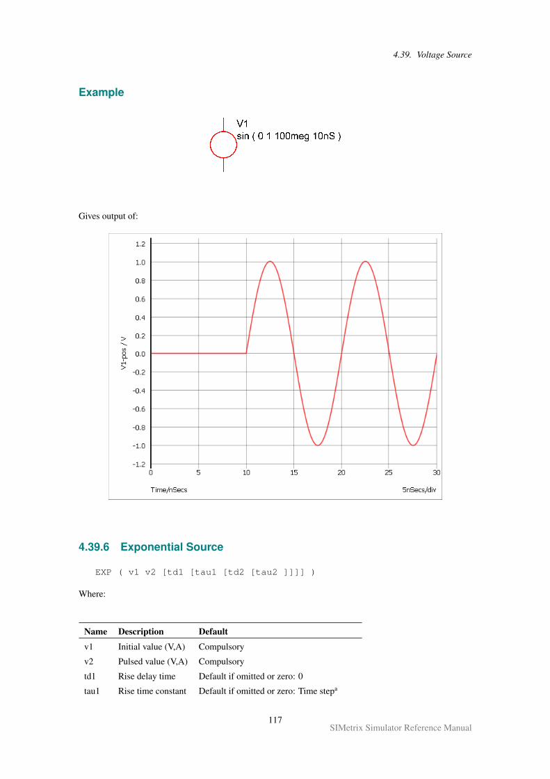
4.39. Voltage Source
Example
Gives output of:
4.39.6 Exponential Source
EXP ( v1 v2 [td1 [tau1 [td2 [tau2 ]]]] )
Where:
Name Description Default
v1 Initial value (V,A) Compulsory
v2 Pulsed value (V,A) Compulsory
td1 Rise delay time Default if omitted or zero: 0
tau1 Rise time constant Default if omitted or zero: Time stepa
117SIMetrix Simulator Reference Manual
4.39. Voltage Source
Name Description Default
td2 Fall delay time Default if omitted or zero: td1 + Time step
tau2 Fall time constant Default if omitted or zero: Time step
a. Time step is set up by the .TRAN simulator directive which defines atransient analysis. Refer to “.TRAN” on page 251.
Defined by:
td1 to td2: v1 + (v2− v1).[1− e−(t−td1)/tau1]
td2 to stop time: v1 + (v2− v1).[1− e−(t−td1)/tau1] + v1 + (v2− v1).[1− e−(t−td2)/tau2]
4.39.7 Single Frequency FM
SFFM ( vo va [fc [mdi [fs ]]] )
Where:
Name Description Default
vo Offset (V,A) Compulsory
va Amplitude (V,A) Compulsory
fc Carrier frequency (Hz) Default if omitted or zero = 1/Stop timea
mdi Modulation index Default if omitted = 0
fs Signal frequency (Hz) Default if omitted or zero = 1/Stop time
a. Stop time refers to the end time of the transient analysis.
Defined by: vo+ va · sin[2π · fc · t+ mdi · sin(2π · fs · t)]
4.39.8 Noise Source
noise interval rms_value [start_time [stop_time]]
Source generates a random value at interval with distribution such that spectrum of signal generated isapproximately flat up to frequency equal to 1/(2*interval). Amplitude of noise is rms_value volts.start_time and stop_time provide a means of specifying a time window over which the source is enabled.Outside this time window, the source will be zero. If stop_time is omitted or zero a value of infinity will beassumed.
4.39.9 Extended PWL Source
PWLS [TIME_SCALE_FACTOR=time_factor] [VALUE_SCALE_FACTOR=value_factor]pwls_spec [ pwls_spec ... ]
Where:
118SIMetrix Simulator Reference Manual
4.39. Voltage Source
time_factor Scales all time values in definition by time_factor
value_factor Scales all magnitude values by value_factor
pwls_spec may be one of the following:
(time, value) Creates a single data point. time is relative tothe current context.
(+time, value) Creates a single data point. time is relative tothe previous point.
REPEAT FOR n pwls_specENDREPEAT
Repeats pwls_spec n times.
REPEAT FOREVER pwls_specENDREPEAT
Repeats pwls_spec forever
SIN sine_parametersEND
Creates a sinusoid. See table below fordefinition of sine_parameters
PULSE pulse_parametersEND
Creates a pulse train. See table below fordefinition of pulse_parameters
FILE file_name Loads a definition from file file_name. If thename contains spaces, it must be quoted
Sine Parameters
Name Description Default Compulsory
FREQ Frequency N/A Yes
PEAK Peak value of sine 1.0 No
OFFSET Offset 0.0 No
DELAY Delay before sine starts. 0.0 No
PHASE Phase 0.0 No
CYCLES Number of cycles. Use -1.0 for infinity -1.0 No
MINPOINTS Minimum number of timesteps used per cycle 13 No
RAMP Frequency ramp factor 0.0 No
The sine value is defined as follows:
if t>0 OR DELAY<0PEAK * SIN(f*2pi*t+PHASE*pi/180) + OFFSET
elsePEAK * SIN(PHASE*pi/180) + OFFSET
Where:
f = FREQ + t×RAMP
t = time - tref - DELAY
time is the global simulation time
tref is the reference time for this spec
119SIMetrix Simulator Reference Manual
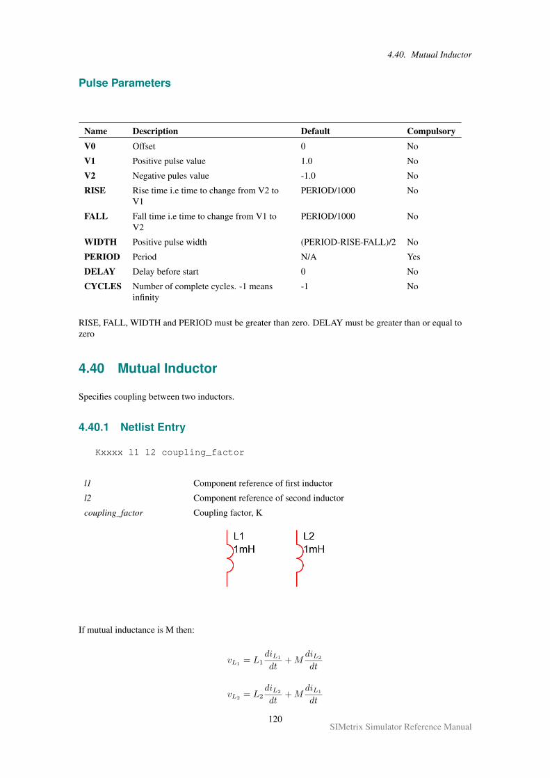
4.40. Mutual Inductor
Pulse Parameters
Name Description Default Compulsory
V0 Offset 0 No
V1 Positive pulse value 1.0 No
V2 Negative pules value -1.0 No
RISE Rise time i.e time to change from V2 toV1
PERIOD/1000 No
FALL Fall time i.e time to change from V1 toV2
PERIOD/1000 No
WIDTH Positive pulse width (PERIOD-RISE-FALL)/2 No
PERIOD Period N/A Yes
DELAY Delay before start 0 No
CYCLES Number of complete cycles. -1 meansinfinity
-1 No
RISE, FALL, WIDTH and PERIOD must be greater than zero. DELAY must be greater than or equal tozero
4.40 Mutual Inductor
Specifies coupling between two inductors.
4.40.1 Netlist Entry
Kxxxx l1 l2 coupling_factor
l1 Component reference of first inductor
l2 Component reference of second inductor
coupling_factor Coupling factor, K
If mutual inductance is M then:
vL1= L1
diL1
dt+M
diL2
dt
vL2= L2
diL2
dt+M
diL1
dt
120SIMetrix Simulator Reference Manual
4.41. Verilog-HDL Interface (VSXA)
K =M√L1 · L2
K cannot be greater than 1.
4.40.2 Notes
You can only couple ideal inductors using this method. The saturable inductor devices may not be coupledin this way. See “Inductor (Saturable)” on page 66 for more information.
To use the mutual inductor directly on a schematic you will need to add the device line to the netlist. See“Adding Extra Netlist Lines” on page 2 for information about how to do this.
If you wish to couple more than two inductors, the coupling coefficient (K value) must be specified forevery possible combination of two inductors. An error will result if this is not done.
For iron cored transformers values of K between 0.99 and 0.999 are typical. For ferrites lower valuesshould be used. If the windings are concentric (i.e. one on top of the other) then 0.98 to 0.99 arereasonable. If the windings are side by side on a sectioned former, K values are lower - perhaps 0.9 to0.95. The addition of air gaps tends to lower K values.
4.40.3 Example
A transformer with 25:1 turns ratio and primary inductance of 10mH
** InductorsLprimary N1 N2 10mLsecondary N3 N4 16u
** Coupling of 0.99 typical for ungapped ferriteK1 Lprimary Lsecondary 0.99
4.41 Verilog-HDL Interface (VSXA)
4.41.1 Overview
The VSXA device provides digital functionality defined by a Verilog-HDL definition. The connections tothe VSXA device map directly to input and output ports defined within the Verilog-HDL module and maybe connected to analog or digital SIMetrix components or other VSXA devices.
The Verilog-HDL simulation is performed by an external Verilog simulator and at least one such simulatoris supplied with SIMetrix and is pre-installed with no additional setup or configuration required.Communication between the external Verilog-HDL simulator is achieved through the VPI programminginterface and in principle this can allow any VPI compliant Verilog-HDL simulator to be used for thispurpose.
This section describes details of the VSXA device. For more general information about using theVerilog-HDL feature, refer to Chapter 13 in the User’s Manual.
Netlist
Uxxxx nodes modelname
121SIMetrix Simulator Reference Manual
4.41. Verilog-HDL Interface (VSXA)
nodes Nodes connecting to Verilog device. Nodes that appear here map directlyto the port connections in the top level module in the Verilog file defined inthe associated .MODEL statement. If the Verilog definition containsvector connections, the sizes of those connections may be defined usingthe PORTSIZES model parameter. See below for details.
modelname Name of model. Used to reference .MODEL statement
Model Syntax
MODEL modelname vsxa parameters
Name Description Units Default
LOAD Path to file name of Verilogdefinition.
n/a Compulsory
IN_LOW Input analog low thresholdvoltage. A logic zero will bedetected when the analogvoltage drops below thisthreshold
V 2.2
IN_HIGH Input analog high thresholdvoltage. A logic one will bedetected when the analogvoltage rises above thisthreshold
V 2.3
OUT_LOW Output voltage for a logiczero
V 0
OUT_HIGH Output voltage for a logicone
V 5
T_RISE Output rise time sec 100p
T_FALL Output fall time sec 100p
IN_RES Input resistance Ohms 1e12
OUT_RES Output resistance for logic zeroand logic one states
Ohms 100
OUT_RES_HIZ Output resistance for the highimpedance state
Ohms 1e12
TIME_TOL Input threshold time tolerance.This parameter works in thesame way as the TIME_TOLparameter defined for the A-DInterface bridge used in thebuilt-in digital simulator. Thisis described in “Time StepControl - TIME_TOLparameter” on page 177
sec 100p
122SIMetrix Simulator Reference Manual
4.41. Verilog-HDL Interface (VSXA)
Name Description Units Default
DISABLE_INTERNAL_VECTORS VSXA instances that areconnected to each other but notto any other SIMetrix devicestill generate digital vectors toallow plotting of those nodes.Setting this parameter to 1disables this
0 (false)
DISABLE_ MODULE_ CACHE No cache data will be createdfor this model.
0 (false)
PORTSIZES Array of values defining thesize of each port. If any of theVerilog ports are vectors,SIMetrix needs to know theirsize. If this parameter is notspecified, it will assume theyare the size defined in theVerilog module. If any isactually smaller, this needs tobe defined in thisparameter.
This is a vector value with onevalue for each port. So if thereare three ports, PORTSIZESwould be set like this forexample:
PORTSIZES=[2,3,5]
which would set the first port tosize 2, the second to size 3 andthe last to size 5
see description
PORTINIT Initial state for input ports if dcsolution lies between in_lowand in_high. This is a vectorvalue with one value for eachinput port. So if there are twoinput ports, PORTINIT wouldbe set like this forexample:
PORTINIT=[1,1]
which would set both ports to alogic one indicating if theanalog input lies between thedefined thresholds. If aPORTINIT value is set to 2, theport will be set to theUNKNOWN state.
Note that vector ports aretreated as one for thisparameter.
0
123SIMetrix Simulator Reference Manual
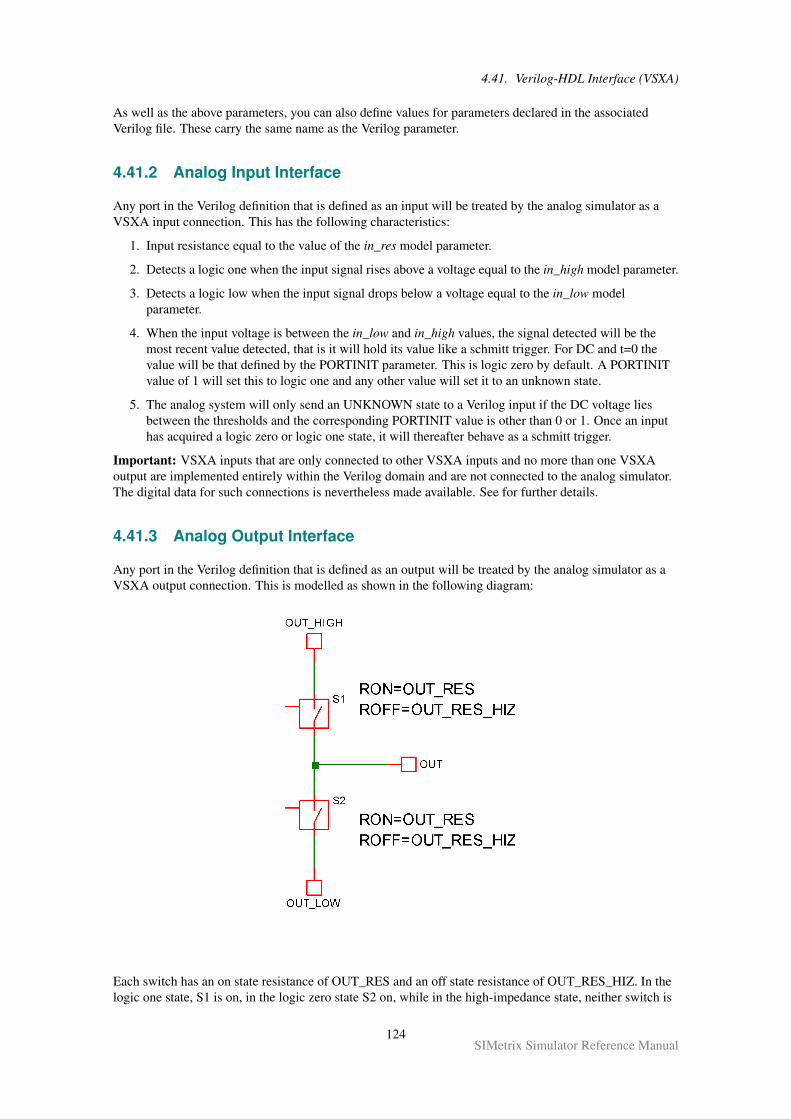
4.41. Verilog-HDL Interface (VSXA)
As well as the above parameters, you can also define values for parameters declared in the associatedVerilog file. These carry the same name as the Verilog parameter.
4.41.2 Analog Input Interface
Any port in the Verilog definition that is defined as an input will be treated by the analog simulator as aVSXA input connection. This has the following characteristics:
1. Input resistance equal to the value of the in_res model parameter.
2. Detects a logic one when the input signal rises above a voltage equal to the in_high model parameter.
3. Detects a logic low when the input signal drops below a voltage equal to the in_low modelparameter.
4. When the input voltage is between the in_low and in_high values, the signal detected will be themost recent value detected, that is it will hold its value like a schmitt trigger. For DC and t=0 thevalue will be that defined by the PORTINIT parameter. This is logic zero by default. A PORTINITvalue of 1 will set this to logic one and any other value will set it to an unknown state.
5. The analog system will only send an UNKNOWN state to a Verilog input if the DC voltage liesbetween the thresholds and the corresponding PORTINIT value is other than 0 or 1. Once an inputhas acquired a logic zero or logic one state, it will thereafter behave as a schmitt trigger.
Important: VSXA inputs that are only connected to other VSXA inputs and no more than one VSXAoutput are implemented entirely within the Verilog domain and are not connected to the analog simulator.The digital data for such connections is nevertheless made available. See for further details.
4.41.3 Analog Output Interface
Any port in the Verilog definition that is defined as an output will be treated by the analog simulator as aVSXA output connection. This is modelled as shown in the following diagram:
Each switch has an on state resistance of OUT_RES and an off state resistance of OUT_RES_HIZ. In thelogic one state, S1 is on, in the logic zero state S2 on, while in the high-impedance state, neither switch is
124SIMetrix Simulator Reference Manual
4.41. Verilog-HDL Interface (VSXA)
on. When transitioning from one state to another state, each switch’s resistance changes linearly to the newstate’s value in the time determined by the parameters T_RISE and T_FALL.
Important: A VSXA output that is only connected to VSXA inputs is implemented entirely within theVerilog domain and are not connected to the analog simulator.
4.41.4 Data Vector Output
Voltage Data
Connections between VSXA devices and any other SIMetrix device (including non-Verilog digitaldevices) are analog nodes in every way and will generate voltage data vectors in the usual way.
Connections between VSXA devices and other VSXA devices that do not connect to anything else and donot connect more than one Verilog module output port are implemented entirely within the Verilogsimulator domain and do not interface to the analog simulator. For such connections, digital data vectorsare created. These transition between the values OUT_LOW and OUT_HIGH with rise and fall timesequal to the timing resolution set by the VerilogResolution option setting. This defaults to 1fs.
In some situations it is possible that the overhead of creating this data could slow down the simulation.This would be the case where such internally connected signals carry high speed data that is much fasterthan the analog time steps. In these cases the output of this data can be disabled using theDISABLE_INTERNAL_VECTORS parameter for the VSXA device that carries the output driving port.They can also be globally disabled using the VerilogDisableInternalVectors .OPTIONS setting.
Current Data
VSXA devices generate current vectors in the normal way for all connections that connect to analogsignals. These vectors are named as follows:
ref#port_name
In the case of vector ports port_name is the name of the port appended with the index of the wire withinthe port. For example, with the following Verilog definition:
module adder(in1, in2, out) ;
input [3:0] in1 ;input [3:0] in2 ;output [3:0] out ;
the port_names for the out port would be out0, out1, out2 and out3.
4.41.5 Module Cache
Operation
Before starting a simulation and also when creating a symbol from a Verilog design, SIMetrix needs togather some information about each Verilog module used in the circuit. It does this by starting a Verilogsimulation then interrogating the Verilog simulator via VPI. This process can take some time if there aremany Verilog modules in the circuit. To speed things up, SIMetrix caches the information obtained forfuture use.
The cache mechanism calculates the MD5 checksum of the Verilog file and stores this with the cachedinformation in the cache file. When the cached information is required, SIMetrix calculates the MD5checksum of the Verilog file and looks to see whether there is a cache item with that MD5 value. If thereis, it will use the cached data. If not it will retrieve the information via the Verilog simulator.
125SIMetrix Simulator Reference Manual
4.42. NXP Compact Models
Location
The cache file is located at vldatapath/module-cache.sxche
Where vldatapath is a directory defined by the VlDataPath global option setting. This can be set using theSet command typed at the command line. E.g.
Set VlDataPath=path
The default value of path is:
simetrix_app_data_dir/veriloghdl
simetrix_app_data_dir is the directory where SIMetrix configuration settings are stored and defaults toC:\Users\login-name\AppData\Roaming. Refer to User’s Manual/Sundry Topics/ConfigurationSettings/Application Data Directory for details about the Application Data path simetrix_app_data_dir.
Be aware that this file is created when a simulation is closed. This takes place when a new simulation isstarted, when the Reset script command is executed or when the simulator process terminates.
Limitations
The cache mechanism only looks at the contents of the Verilog file referenced. It does not take account ofinclude files for example. However, the only information stored in the cache are the module name, namesand direction of the module ports and the names, types and default values of any parameters. It would beususual to store these items in an include file but of course this is perfectly legal.
If the top level ports or/and parameters for your Verilog design are nor defined in the main file but in aninclude file, then you should either redesign the Verilog file or alternatively disable the cache for thatmodule.
The cache can be disabled by setting the DISABLE_MODULE_CACHE model parameter. Important:the DISABLE_MODULE_CACHE parameter disables the creation of cached information; it does notdisable using cached information if it already exists. This is because the cache is read before modelparameters are read. You may wish to clear the cache altogether when setting this parameter. This can bedone from the front end with menu Verilog | Clear Verilog-HDL Module Info Cache.
The cache can also be globally disabled using the .OPTIONS setting VerilogDisableModuleCache.
4.42 NXP Compact Models
4.42.1 Introduction
SIMetrix supports a range of device models developed by NXP Semiconductor.
The table below shows the models available. Model statements should be in the form:
.model model_name model_type_name LEVEL=level_number parameters
E.g.
.model my_model nmos LEVEL=103 ...
defines a MOS 9 nmos device.
To instantiate the device line must start with the letter as defined in the Device Letter column in the tablebelow. The number of nodes must be within the range specified in the table.
126SIMetrix Simulator Reference Manual
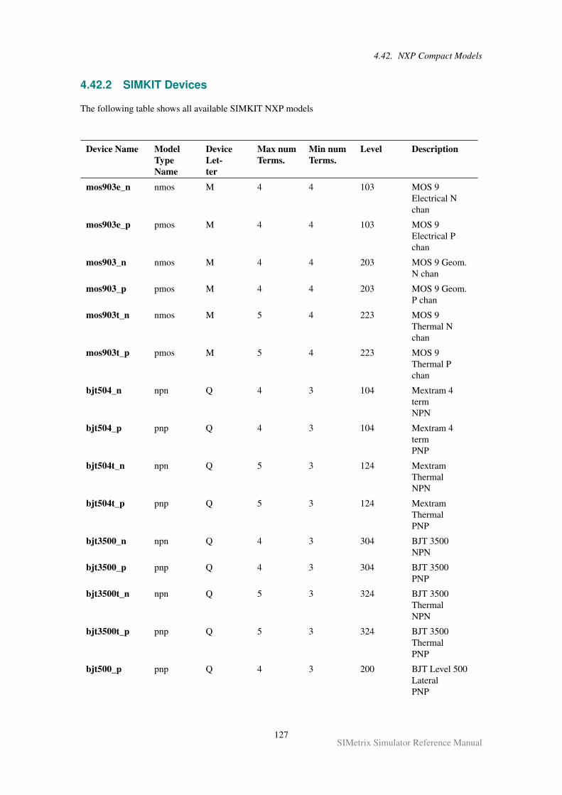
4.42. NXP Compact Models
4.42.2 SIMKIT Devices
The following table shows all available SIMKIT NXP models
Device Name ModelTypeName
DeviceLet-ter
Max numTerms.
Min numTerms.
Level Description
mos903e_n nmos M 4 4 103 MOS 9Electrical Nchan
mos903e_p pmos M 4 4 103 MOS 9Electrical Pchan
mos903_n nmos M 4 4 203 MOS 9 Geom.N chan
mos903_p pmos M 4 4 203 MOS 9 Geom.P chan
mos903t_n nmos M 5 4 223 MOS 9Thermal Nchan
mos903t_p pmos M 5 4 223 MOS 9Thermal Pchan
bjt504_n npn Q 4 3 104 Mextram 4termNPN
bjt504_p pnp Q 4 3 104 Mextram 4termPNP
bjt504t_n npn Q 5 3 124 MextramThermalNPN
bjt504t_p pnp Q 5 3 124 MextramThermalPNP
bjt3500_n npn Q 4 3 304 BJT 3500NPN
bjt3500_p pnp Q 4 3 304 BJT 3500PNP
bjt3500t_n npn Q 5 3 324 BJT 3500ThermalNPN
bjt3500t_p pnp Q 5 3 324 BJT 3500ThermalPNP
bjt500_p pnp Q 4 3 200 BJT Level 500LateralPNP
127SIMetrix Simulator Reference Manual
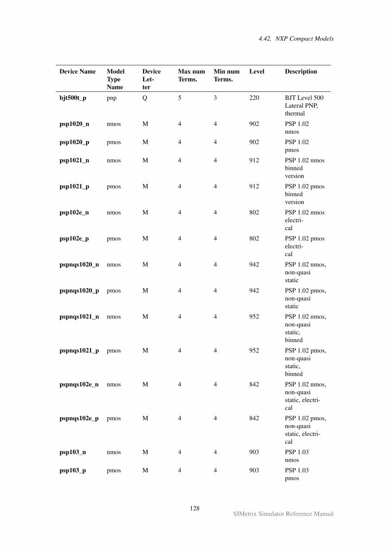
4.42. NXP Compact Models
Device Name ModelTypeName
DeviceLet-ter
Max numTerms.
Min numTerms.
Level Description
bjt500t_p pnp Q 5 3 220 BJT Level 500Lateral PNP,thermal
psp1020_n nmos M 4 4 902 PSP 1.02nmos
psp1020_p pmos M 4 4 902 PSP 1.02pmos
psp1021_n nmos M 4 4 912 PSP 1.02 nmosbinnedversion
psp1021_p pmos M 4 4 912 PSP 1.02 pmosbinnedversion
psp102e_n nmos M 4 4 802 PSP 1.02 nmoselectri-cal
psp102e_p pmos M 4 4 802 PSP 1.02 pmoselectri-cal
pspnqs1020_n nmos M 4 4 942 PSP 1.02 nmos,non-quasistatic
pspnqs1020_p pmos M 4 4 942 PSP 1.02 pmos,non-quasistatic
pspnqs1021_n nmos M 4 4 952 PSP 1.02 nmos,non-quasistatic,binned
pspnqs1021_p pmos M 4 4 952 PSP 1.02 pmos,non-quasistatic,binned
pspnqs102e_n nmos M 4 4 842 PSP 1.02 nmos,non-quasistatic, electri-cal
pspnqs102e_p pmos M 4 4 842 PSP 1.02 pmos,non-quasistatic, electri-cal
psp103_n nmos M 4 4 903 PSP 1.03nmos
psp103_p pmos M 4 4 903 PSP 1.03pmos
128SIMetrix Simulator Reference Manual
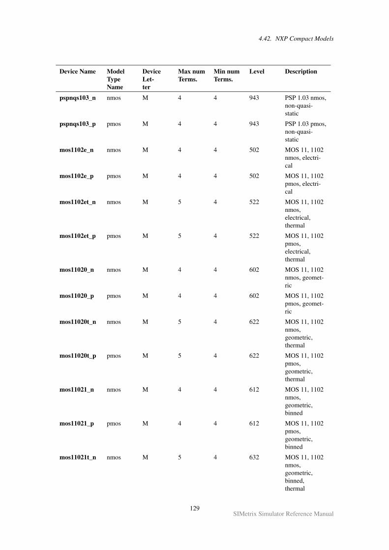
4.42. NXP Compact Models
Device Name ModelTypeName
DeviceLet-ter
Max numTerms.
Min numTerms.
Level Description
pspnqs103_n nmos M 4 4 943 PSP 1.03 nmos,non-quasi-static
pspnqs103_p pmos M 4 4 943 PSP 1.03 pmos,non-quasi-static
mos1102e_n nmos M 4 4 502 MOS 11, 1102nmos, electri-cal
mos1102e_p pmos M 4 4 502 MOS 11, 1102pmos, electri-cal
mos1102et_n nmos M 5 4 522 MOS 11, 1102nmos,electrical,thermal
mos1102et_p pmos M 5 4 522 MOS 11, 1102pmos,electrical,thermal
mos11020_n nmos M 4 4 602 MOS 11, 1102nmos, geomet-ric
mos11020_p pmos M 4 4 602 MOS 11, 1102pmos, geomet-ric
mos11020t_n nmos M 5 4 622 MOS 11, 1102nmos,geometric,thermal
mos11020t_p pmos M 5 4 622 MOS 11, 1102pmos,geometric,thermal
mos11021_n nmos M 4 4 612 MOS 11, 1102nmos,geometric,binned
mos11021_p pmos M 4 4 612 MOS 11, 1102pmos,geometric,binned
mos11021t_n nmos M 5 4 632 MOS 11, 1102nmos,geometric,binned,thermal
129SIMetrix Simulator Reference Manual
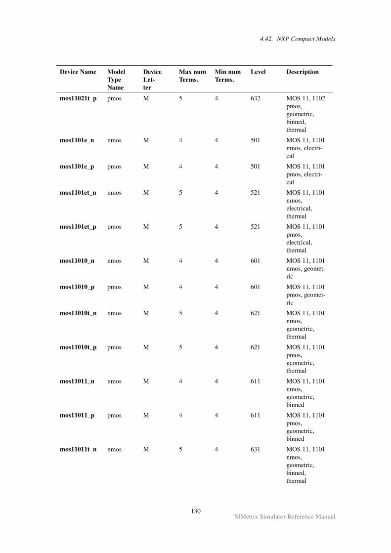
4.42. NXP Compact Models
Device Name ModelTypeName
DeviceLet-ter
Max numTerms.
Min numTerms.
Level Description
mos11021t_p pmos M 5 4 632 MOS 11, 1102pmos,geometric,binned,thermal
mos1101e_n nmos M 4 4 501 MOS 11, 1101nmos, electri-cal
mos1101e_p pmos M 4 4 501 MOS 11, 1101pmos, electri-cal
mos1101et_n nmos M 5 4 521 MOS 11, 1101nmos,electrical,thermal
mos1101et_p pmos M 5 4 521 MOS 11, 1101pmos,electrical,thermal
mos11010_n nmos M 4 4 601 MOS 11, 1101nmos, geomet-ric
mos11010_p pmos M 4 4 601 MOS 11, 1101pmos, geomet-ric
mos11010t_n nmos M 5 4 621 MOS 11, 1101nmos,geometric,thermal
mos11010t_p pmos M 5 4 621 MOS 11, 1101pmos,geometric,thermal
mos11011_n nmos M 4 4 611 MOS 11, 1101nmos,geometric,binned
mos11011_p pmos M 4 4 611 MOS 11, 1101pmos,geometric,binned
mos11011t_n nmos M 5 4 631 MOS 11, 1101nmos,geometric,binned,thermal
130SIMetrix Simulator Reference Manual
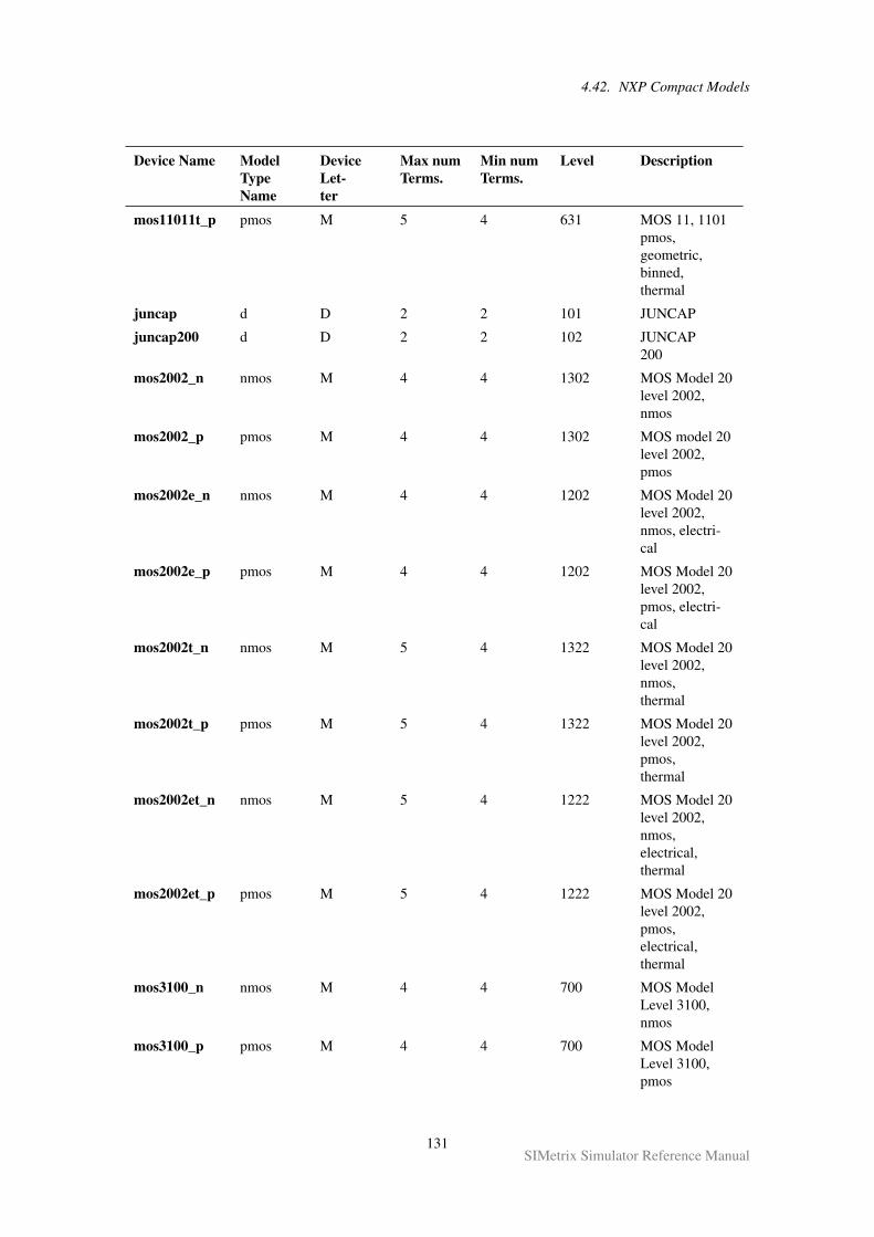
4.42. NXP Compact Models
Device Name ModelTypeName
DeviceLet-ter
Max numTerms.
Min numTerms.
Level Description
mos11011t_p pmos M 5 4 631 MOS 11, 1101pmos,geometric,binned,thermal
juncap d D 2 2 101 JUNCAP
juncap200 d D 2 2 102 JUNCAP200
mos2002_n nmos M 4 4 1302 MOS Model 20level 2002,nmos
mos2002_p pmos M 4 4 1302 MOS model 20level 2002,pmos
mos2002e_n nmos M 4 4 1202 MOS Model 20level 2002,nmos, electri-cal
mos2002e_p pmos M 4 4 1202 MOS Model 20level 2002,pmos, electri-cal
mos2002t_n nmos M 5 4 1322 MOS Model 20level 2002,nmos,thermal
mos2002t_p pmos M 5 4 1322 MOS Model 20level 2002,pmos,thermal
mos2002et_n nmos M 5 4 1222 MOS Model 20level 2002,nmos,electrical,thermal
mos2002et_p pmos M 5 4 1222 MOS Model 20level 2002,pmos,electrical,thermal
mos3100_n nmos M 4 4 700 MOS ModelLevel 3100,nmos
mos3100_p pmos M 4 4 700 MOS ModelLevel 3100,pmos
131SIMetrix Simulator Reference Manual
4.42. NXP Compact Models
Device Name ModelTypeName
DeviceLet-ter
Max numTerms.
Min numTerms.
Level Description
mos3100t_n nmos M 5 4 720 MOS ModelLevel 3100,nmos,thermal
mos3100t_p pmos M 5 4 720 MOS ModelLevel 3100,pmos,thermal
mos40_n nmos M 4 4 400 MOS modelLevel 40,nmos
mos40_p pmos M 4 4 400 MOS modelLevel 40,pmos
mos40t_n nmos M 5 4 420 MOS modelLevel 40, nmos,thermal
mos40t_p pmos M 5 4 420 MOS modelLevel 40, pmos,thermal
4.42.3 Notes on SIMKIT Models
Binned Models
Binned models are not yet integrated with the library binning system. So, to use the binning features ofbinned models, you will need to manually generate separate model names for each bin.
Real Time Noise
Some models do not fully implement real-time noise. Many MOS models include frequency dependentgate noise and this is not included in real-time noise analyses. Also some models include correlated noisewhich is also not included. In most cases these effects are small anyway and have little effect.
You can set this option in AC small-signal noise:
.options noMos9GateNoise
to disable the same effects in AC small signal noise. A comparison can then be made to estimate the effectthese noise sources may have in real-time noise. Although the option name suggests that it only applies toMOS9, this does in fact work with all applicable models.
In the case of PSP 102 models, you can instead invoke the Verilog-A based model which fully supports allnoise effects in real-time noise analysis. See next section for details.
132SIMetrix Simulator Reference Manual

4.42. NXP Compact Models
PSP 102
The PSP 102 nmos and pmos geometric models (level 902) are also available as level 1023. However thetwo models are implemented differently. Level 902 is implemented through the SIMKIT interface. Themodel code itself in this case is created using ADMS from the Verilog-A description. However, it seemsthat the noise model for this is not created from the Verilog-A code and appears to have been hand coded.
The Level 1023 version is built entirely from the Verilog-A code using the SIMetrix Verilog-A compilerbut using a more advanced commercial C-compiler than the open source version supplied with SIMetrix.This version has the benefit over the Simkit version that it fully supports real-time noise includingcorrelated effects and gate noise. It is however a little slower - typically about 5-10% compared to theSIMKIT version.
We have done extensive side by side tests of both models and both give identical results to a high degree ofaccuracy.
Older Models
Older “Philips Compact Models” (PCM) devices are no longer supported. Nearly all of the original PCMdevices have been replaced by Simkit devices that are functionally identical. The following devices are notavailable in the Simkit library:
MOS 9 version 9.02 devices are no longer available, however, version 9.03 is fully backward compatible.Version 9.03 is available in the Simkit library. Version 9.02 was previously accessed using levels 102 and202. These level numbers now map to version 9.03. The only change in behaviour is that some newversion 9.03 parameters will be accepted correctly without error.
Mextram 5.03 is no longer available. Superseded by 5.04 but this is not directly compatible.
Diode level 200 is no longer available.
MOS 11 SIMetrix level 500/600 is no longer available. Superseded by 501/601. Currently no informationis available as to whether or not the new version is backward compatible.
MOS level 302 is no longer available.
133SIMetrix Simulator Reference Manual
5.1. Device Overview
Chapter 5
Digital/Mixed Signal Device Reference
5.1 Digital Device Overview
5.1.1 Common Parameters
A number of model parameters are common to most of the digital models. These are described below.
Family Parameters
These identify the logic family to which the input and outputs belong. See “Logic families” on page 290for a detailed explanation. Most models have three family parameters:
Family name Description
in_family Specifies family for inputs. If omitted, the input family is specified by theFAMILY parameter
out_family Specifies family for outputs. If omitted, the output family is specified bythe FAMILY parameter
family Default value for IN_FAMILY and OUT_FAMILY
Output Parameters
Parameter name Description
out_res This is used to calculate loading delay. It has dimensions of Ohms so isreferred to as a resistance. The additional loading delay is calculated bymultiplying OUT_RES by the total capacitative load detected on the nodeto which the output connects.
min_sink Used to calculate static loading effects. This is the current that the deviceis able to sink. Current flowing out of the pin is positive so this parameteris usually negative. If the total sink load current is arithmetically smaller(i.e. more negative) than this parameter then the output will be forced toan UNKNOWN state. This is used to implement fan out limitations inbipolar logic.
134SIMetrix Simulator Reference Manual
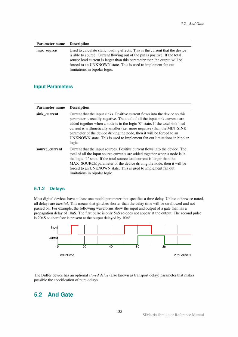
5.2. And Gate
Parameter name Description
max_source Used to calculate static loading effects. This is the current that the deviceis able to source. Current flowing out of the pin is positive. If the totalsource load current is larger than this parameter then the output will beforced to an UNKNOWN state. This is used to implement fan outlimitations in bipolar logic.
Input Parameters
Parameter name Description
sink_current Current that the input sinks. Positive current flows into the device so thisparameter is usually negative. The total of all the input sink currents areadded together when a node is in the logic ‘0’ state. If the total sink loadcurrent is arithmetically smaller (i.e. more negative) than the MIN_SINKparameter of the device driving the node, then it will be forced to anUNKNOWN state. This is used to implement fan out limitations in bipolarlogic.
source_current Current that the input sources. Positive current flows into the device. Thetotal of all the input source currents are added together when a node is inthe logic ‘1’ state. If the total source load current is larger than theMAX_SOURCE parameter of the device driving the node, then it will beforced to an UNKNOWN state. This is used to implement fan outlimitations in bipolar logic.
5.1.2 Delays
Most digital devices have at least one model parameter that specifies a time delay. Unless otherwise noted,all delays are inertial. This means that glitches shorter than the delay time will be swallowed and notpassed on. For example, the following waveforms show the input and output of a gate that has apropagation delay of 10nS. The first pulse is only 5nS so does not appear at the output. The second pulseis 20nS so therefore is present at the output delayed by 10nS.
The Buffer device has an optional stored delay (also known as transport delay) parameter that makespossible the specification of pure delays.
5.2 And Gate
135SIMetrix Simulator Reference Manual
5.2. And Gate
5.2.1 Netlist entry:
Axxxx [ in_0 in_1 .. in_n ] out model_name
5.2.2 Connection details
Name Description Flow Type Vector bounds
in Input in d, vector 2−∞out Output out d n/a
5.2.3 Model format
.MODEL model_name d_and parameters
5.2.4 Model parameters
Name Description Type Default Limits
rise_delay Rise delay real 1nS 1e-12 -∞fall_delay Fall delay real 1nS 1e-12 -∞input_load Input load value (F) real 1pF none
family Logic family string UNIV none
in_family Input logic family string UNIV none
out_family Output logic family string UNIV none
out_res Digital output resistance real 100 0−∞out_res_pos Digital output res. pos. slope real out_res 0−∞out_res_neg Digital output res. neg. slope out_res 0−∞open_c Open collector output boolean FALSE none
min_sink Minimum sink current real -0.001 none
max_source Maximum source current real 0.001 none
sink_current Input sink current real 0 none
source_current Input source current real 0 none
5.2.5 Device operation
• If the model parameter OPEN_C is false, The output will be at logic ‘0’ if either input is at logic ‘0’.Otherwise, if any input is UNKNOWN, the output will be UNKNOWN. Otherwise the output willbe at logic ‘1’.
• If the model parameter OPEN_C is true the device will be open collector. In this case the outputlogic state is always ‘0’. The state of the inputs instead determines the strength of the output. Ifeither input is at logic ‘0’ the output strength will be STRONG. Otherwise if any input isUNKNOWN the output strength will be UNDETERMINED. Otherwise the output strength will beHI-IMPEDANCE allowing a pull-up resistor to force it to the logic ‘1’ state.
136SIMetrix Simulator Reference Manual
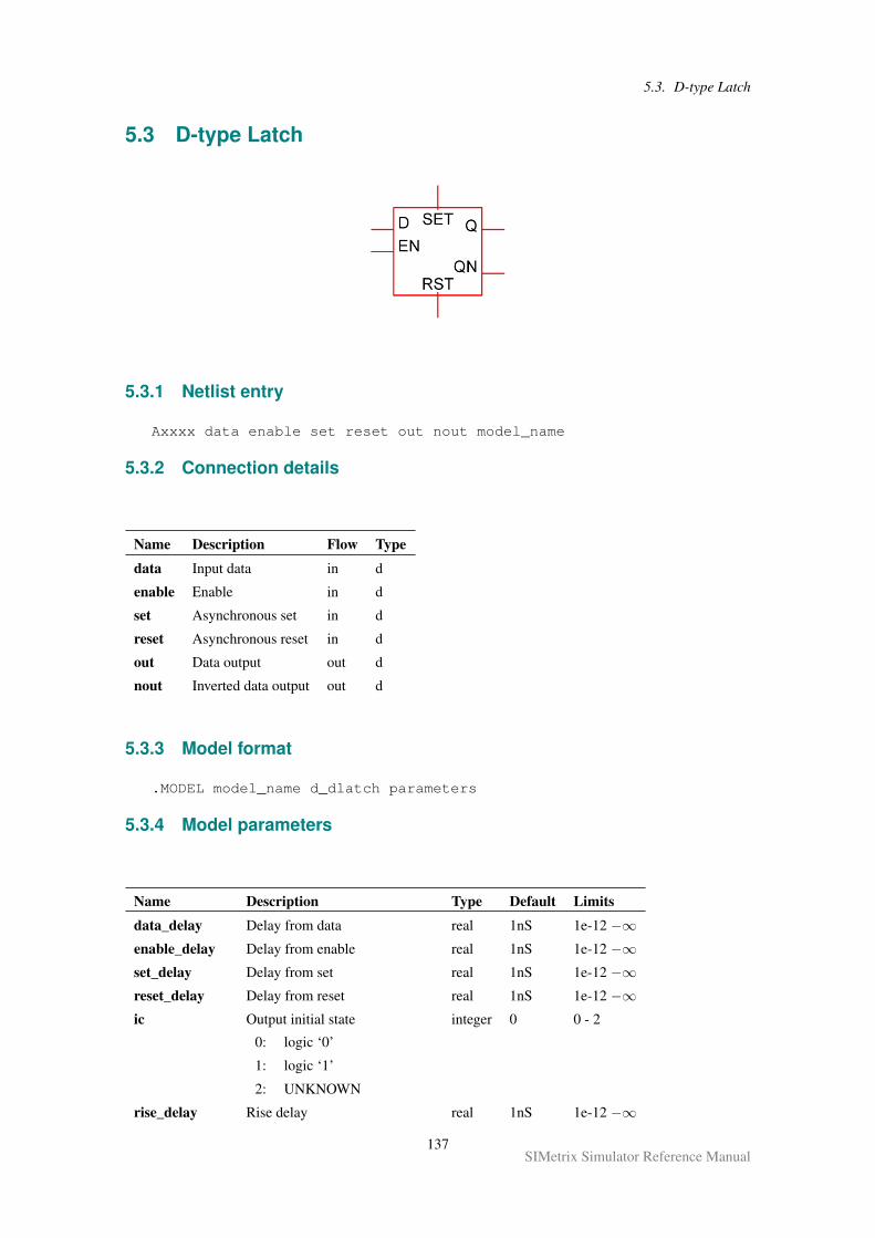
5.3. D-type Latch
5.3 D-type Latch
5.3.1 Netlist entry
Axxxx data enable set reset out nout model_name
5.3.2 Connection details
Name Description Flow Type
data Input data in d
enable Enable in d
set Asynchronous set in d
reset Asynchronous reset in d
out Data output out d
nout Inverted data output out d
5.3.3 Model format
.MODEL model_name d_dlatch parameters
5.3.4 Model parameters
Name Description Type Default Limits
data_delay Delay from data real 1nS 1e-12 −∞enable_delay Delay from enable real 1nS 1e-12 −∞set_delay Delay from set real 1nS 1e-12 −∞reset_delay Delay from reset real 1nS 1e-12 −∞ic Output initial state
0: logic ‘0’
1: logic ‘1’
2: UNKNOWN
integer 0 0 - 2
rise_delay Rise delay real 1nS 1e-12 −∞
137SIMetrix Simulator Reference Manual
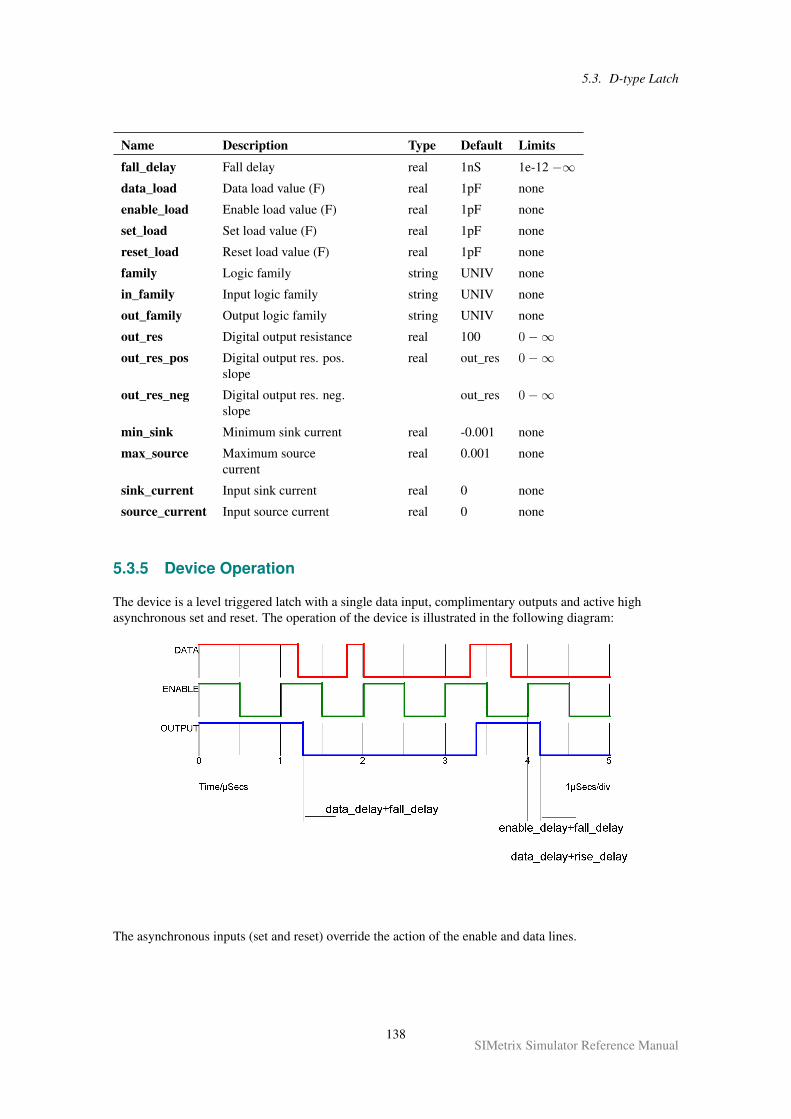
5.3. D-type Latch
Name Description Type Default Limits
fall_delay Fall delay real 1nS 1e-12 −∞data_load Data load value (F) real 1pF none
enable_load Enable load value (F) real 1pF none
set_load Set load value (F) real 1pF none
reset_load Reset load value (F) real 1pF none
family Logic family string UNIV none
in_family Input logic family string UNIV none
out_family Output logic family string UNIV none
out_res Digital output resistance real 100 0−∞out_res_pos Digital output res. pos.
slopereal out_res 0−∞
out_res_neg Digital output res. neg.slope
out_res 0−∞
min_sink Minimum sink current real -0.001 none
max_source Maximum sourcecurrent
real 0.001 none
sink_current Input sink current real 0 none
source_current Input source current real 0 none
5.3.5 Device Operation
The device is a level triggered latch with a single data input, complimentary outputs and active highasynchronous set and reset. The operation of the device is illustrated in the following diagram:
The asynchronous inputs (set and reset) override the action of the enable and data lines.
138SIMetrix Simulator Reference Manual
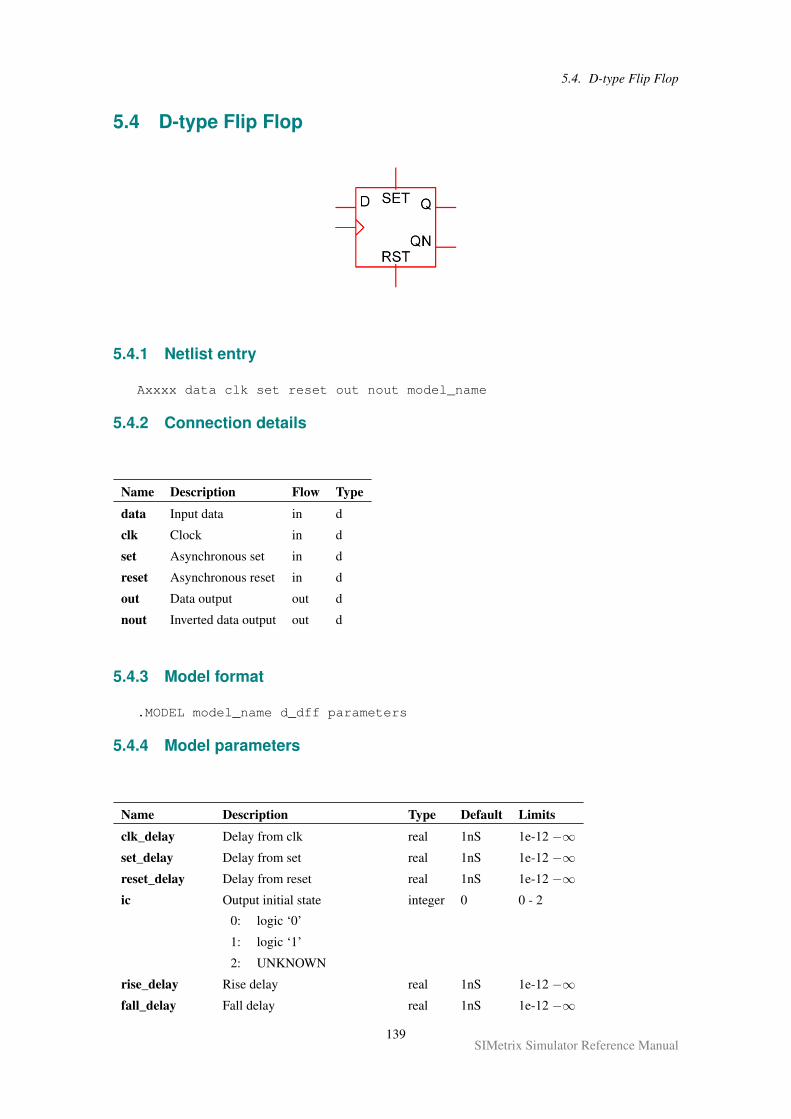
5.4. D-type Flip Flop
5.4 D-type Flip Flop
5.4.1 Netlist entry
Axxxx data clk set reset out nout model_name
5.4.2 Connection details
Name Description Flow Type
data Input data in d
clk Clock in d
set Asynchronous set in d
reset Asynchronous reset in d
out Data output out d
nout Inverted data output out d
5.4.3 Model format
.MODEL model_name d_dff parameters
5.4.4 Model parameters
Name Description Type Default Limits
clk_delay Delay from clk real 1nS 1e-12 −∞set_delay Delay from set real 1nS 1e-12 −∞reset_delay Delay from reset real 1nS 1e-12 −∞ic Output initial state
0: logic ‘0’
1: logic ‘1’
2: UNKNOWN
integer 0 0 - 2
rise_delay Rise delay real 1nS 1e-12 −∞fall_delay Fall delay real 1nS 1e-12 −∞
139SIMetrix Simulator Reference Manual
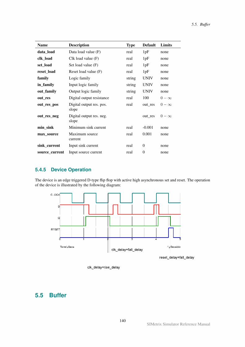
5.5. Buffer
Name Description Type Default Limits
data_load Data load value (F) real 1pF none
clk_load Clk load value (F) real 1pF none
set_load Set load value (F) real 1pF none
reset_load Reset load value (F) real 1pF none
family Logic family string UNIV none
in_family Input logic family string UNIV none
out_family Output logic family string UNIV none
out_res Digital output resistance real 100 0−∞out_res_pos Digital output res. pos.
slopereal out_res 0−∞
out_res_neg Digital output res. neg.slope
out_res 0−∞
min_sink Minimum sink current real -0.001 none
max_source Maximum sourcecurrent
real 0.001 none
sink_current Input sink current real 0 none
source_current Input source current real 0 none
5.4.5 Device Operation
The device is an edge triggered D-type flip flop with active high asynchronous set and reset. The operationof the device is illustrated by the following diagram:
5.5 Buffer
140SIMetrix Simulator Reference Manual
5.5. Buffer
5.5.1 Netlist entry
Axxxx in out model_name
5.5.2 Connection details
Name Description Flow Type
in Input in d
out Output out d
5.5.3 Model format
.MODEL model_name d_buffer parameters
5.5.4 Model parameters
Name Description Type Default Limits
rise_delay Rise delay real 1nS 1e-12 −∞fall_delay Fall delay real 1nS 1e-12 −∞stored_delay Stored delay (overrides rise_delay and
fall_delay)real 0 0−∞
input_load Input load value (F) real 1pF none
family Logic family string UNIV none
in_family Input logic family string UNIV none
out_family Output logic family string UNIV none
out_res Digital output resistance real 100 0−∞out_res_pos Digital output res. pos. slope real out_res 0−∞out_res_neg Digital output res. neg. slope out_res 0−∞open_c Open collector output boolean FALSE none
min_sink Minimum sink current real -0.001 none
max_source Maximum source current real 0.001 none
sink_current Input sink current real 0 none
source_current Input source current real 0 none
open_e Open emitter output boolean FALSE none
5.5.5 Device Operation
This device is a simple buffer with a single input and output. It can optionally be specified to have an opencollector (open_c parameter) or open emitter (open_e parameter) output. Further, if the stored_delayparameter is specified, the device will act as a pure delay. This means that it will pass pulses that areshorter than the delay time whereas normally (delay specified by rise_delay and fall_delay) such pulsewould be swallowed (stored_delay is also known as transport delay).
141SIMetrix Simulator Reference Manual
5.6. Frequency Divider
The following table describes the device operation in detail
OPEN_Cparameter
OPEN_Eparameter
Input Output state Output strength
FALSE FALSE 0 0 STRONG
FALSE FALSE 1 1 STRONG
FALSE FALSE UNKNOWN UNKNOWN STRONG
FALSE TRUE 0 0 HI-IMPEDANCE
FALSE TRUE 1 1 STRONG
FALSE TRUE UNKNOWN UNKNOWN UNDETERMINED
TRUE FALSE 0 0 STRONG
TRUE FALSE 1 0 HI-IMPEDANCE
TRUE FALSE UNKNOWN 0 UNDETERMINED
TRUE TRUE 0 1 HI-IMPEDANCE
TRUE TRUE 1 0 HI-IMPEDANCE
TRUE TRUE UNKNOWN UNKNOWN UNDETERMINED
Note the difference between open emitter and open collector operation. These modes have been designedto be as close to as possible to real devices, in particular their behaviour into an open circuit. An openemitter output, when switching from high to low is likely to follow the voltage on the device’s base due tothe base-emitter capacitance so the output state follows the input state. An open collector (or open drain)output on the other hand will remain in the low state when its input switches.
5.6 Frequency Divider
5.6.1 Netlist entry
Axxxx freq_in freq_out model_name
5.6.2 Connection details
Name Description Flow Type
freq_in Frequency input in d
freq_out Frequency output out d
142SIMetrix Simulator Reference Manual
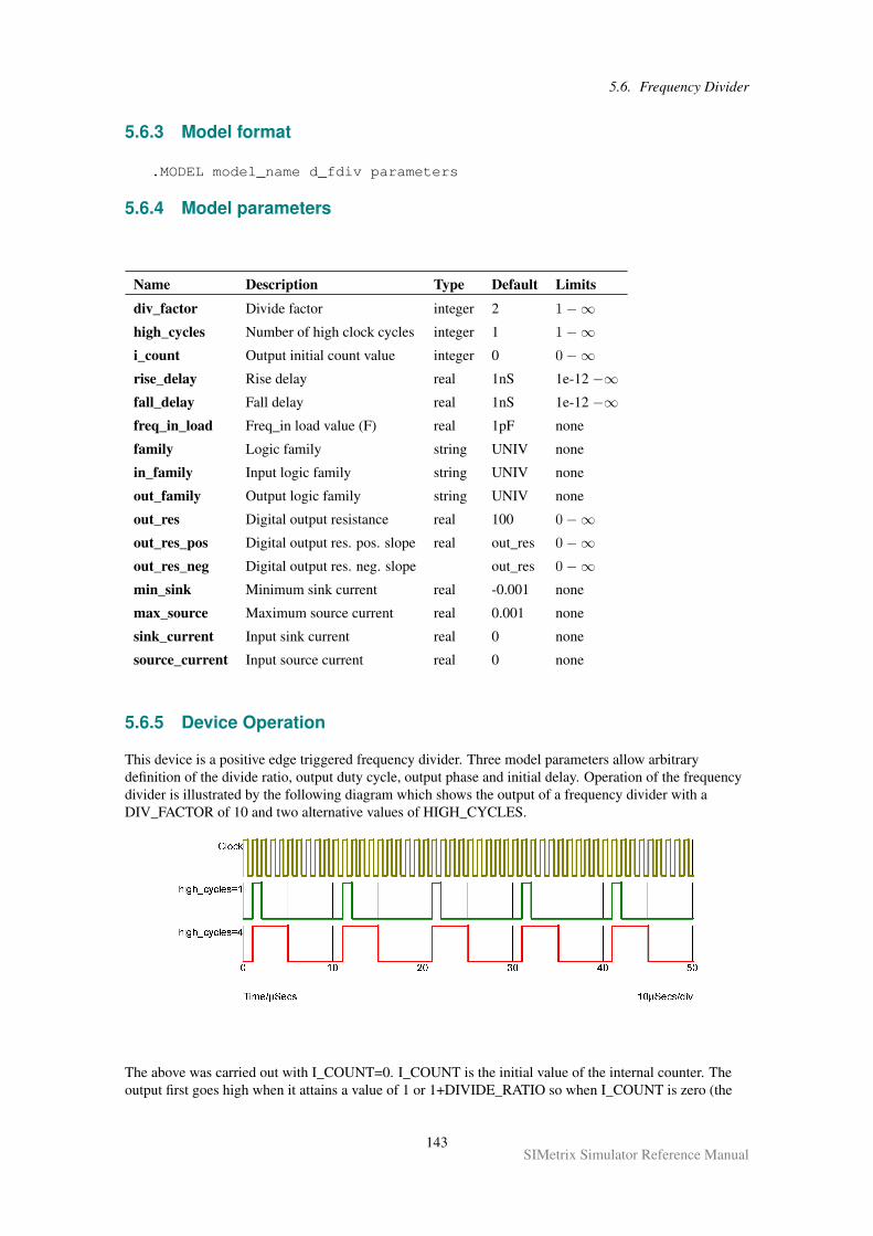
5.6. Frequency Divider
5.6.3 Model format
.MODEL model_name d_fdiv parameters
5.6.4 Model parameters
Name Description Type Default Limits
div_factor Divide factor integer 2 1−∞high_cycles Number of high clock cycles integer 1 1−∞i_count Output initial count value integer 0 0−∞rise_delay Rise delay real 1nS 1e-12 −∞fall_delay Fall delay real 1nS 1e-12 −∞freq_in_load Freq_in load value (F) real 1pF none
family Logic family string UNIV none
in_family Input logic family string UNIV none
out_family Output logic family string UNIV none
out_res Digital output resistance real 100 0−∞out_res_pos Digital output res. pos. slope real out_res 0−∞out_res_neg Digital output res. neg. slope out_res 0−∞min_sink Minimum sink current real -0.001 none
max_source Maximum source current real 0.001 none
sink_current Input sink current real 0 none
source_current Input source current real 0 none
5.6.5 Device Operation
This device is a positive edge triggered frequency divider. Three model parameters allow arbitrarydefinition of the divide ratio, output duty cycle, output phase and initial delay. Operation of the frequencydivider is illustrated by the following diagram which shows the output of a frequency divider with aDIV_FACTOR of 10 and two alternative values of HIGH_CYCLES.
The above was carried out with I_COUNT=0. I_COUNT is the initial value of the internal counter. Theoutput first goes high when it attains a value of 1 or 1+DIVIDE_RATIO so when I_COUNT is zero (the
143SIMetrix Simulator Reference Manual
5.8. Digital Pulse
default) the output first goes high after the first rising edge. If I_COUNT is set to 5 the output first goeshigh after the 6th rising edge and if I_COUNT is -20, the 21st rising edge.
5.7 Digital Initial Condition
5.7.1 Netlist entry
Axxxx out model_name
5.7.2 Connection details
Name Description Flow Type
out Output out d
5.7.3 Model format
.MODEL model_name d_init parameters
5.7.4 Model parameters
Name Description Type Default Limits
ic Initial state integer 0 none
is Initial strength 1 = STRONG 0 = RESISTIVE integer 1 none
out_family Output logic family string UNIV none
5.7.5 Device Operation
This device has the defined initial state (IC parameter) and initial strength (IS parameter) during the DCoperating point solution, then reverts to HI-IMPEDANCE for the remainder of the analysis.
5.8 Digital Pulse
5.8.1 Netlist entry
Axxxx out model_name : parameters
5.8.2 Connection details
Name Description Flow Type
out Output out d
144SIMetrix Simulator Reference Manual
5.9. Digital Signal Source
5.8.3 Instance parameters
Name Description Type
period Pulse period real
delay Delay real
duty Duty cycle real
width Pulse width real
open_out Open emitter output boolean
5.8.4 Model format
.MODEL model_name d_pulse parameters
5.8.5 Model parameters
Name Description Type Default Limits
duty Duty cycle real 0.5 1e-06 - 0.999999
delay Initial delay real 0 0−∞period Period. If zero, a single pulse will be
outputreal 1µS 1e-12 −∞
width Pulse width (overrides duty ifspecified)
real period * duty 0−∞
open_out Open emitter output boolean FALSE none
out_family Output logic family string UNIV none
out_res Digital output resistance real 100 0−∞out_res_pos Digital output res. pos. slope real out_res 0−∞out_res_neg Digital output res. neg. slope out_res 0−∞min_sink Minimum sink current real -0.001 none
max_source Maximum source current real 0.001 none
5.8.6 Device Operation
This device supplies a repetitive or single pulse of defined period, delay and width. Optionally, the devicemay be specified to have an open emitter output allowing several pulse sources to be wire OR’ed to createcomplex pulses. All 5 main .MODEL parameters may also be specified on the device line as instanceparameters in which case they override any values specified in the .MODEL statement.
If OPEN_OUT is specified and true, a pull down resistor must be connected to the output.
5.9 Digital Signal Source
145SIMetrix Simulator Reference Manual
5.9. Digital Signal Source
5.9.1 Netlist entry
Axxxx [ out_0 out_1 .. out_n ] model_name
5.9.2 Connection details
Name Description Flow Type
out Output out d, vector
5.9.3 Model format
.MODEL model_name d_source parameters
5.9.4 Model parameters
Name Description Type Default Limits
input_file Digital input vector filename string none none
out_family Output logic family string UNIV none
out_res Digital output resistance real 100 0−∞out_res_pos Digital output res. pos. slope real out_res 0−∞out_res_neg Digital output res. neg. slope out_res 0−∞min_sink Minimum sink current real -0.001 none
max_source Maximum source current real 0.001 none
5.9.5 Device Operation
The digital signal source provides a multi bit arbitrary digital signal defined in a file.
5.9.6 File Format
The file is in ASCII format and is in the form of a table each row being on a new line. The first columndefines the time values while the entries in the remaining columns define the output value for each of theoutputs. So the total number of columns must be the number of outputs plus one. The output values mustappear in the same order as the outputs in the netlist entry. So, the values for out_0 will be in column 2,out_1 in column 3 etc.
The file may include blank lines and comment lines beginning with a ‘*’.
The output values must specify the state as well as the strength using the following codes:
Code State-Strength
0S LOW-STRONG
1S HIGH-STRONG
146SIMetrix Simulator Reference Manual
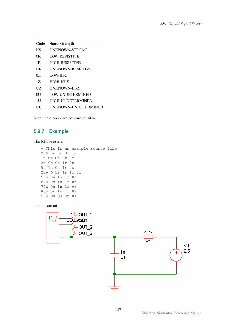
5.9. Digital Signal Source
Code State-Strength
US UNKNOWN-STRONG
0R LOW-RESISTIVE
1R HIGH-RESISTIVE
UR UNKNOWN-RESISTIVE
0Z LOW-HI-Z
1Z HIGH-HI-Z
UZ UNKNOWN-HI-Z
0U LOW-UNDETERMINED
1U HIGH-UNDETERMINED
UU UNKNOWN-UNDETERMINED
Note, these codes are not case sensitive.
5.9.7 Example
The following file:
* This is an example source file0.0 0s 0s 0r 1s1u 0s 0s 0r 0z2u 0s 0s 1r 0z5u 1s 0s 1r 0z22e-6 1s 1s 1r 0z50u 0s 1s 1r 0z60u 0s 1s 1r 0z70u 0s 1s 1r 0z80u 0s 1s 1r 0z90u Us Us Ur 0s
and this circuit:
147SIMetrix Simulator Reference Manual
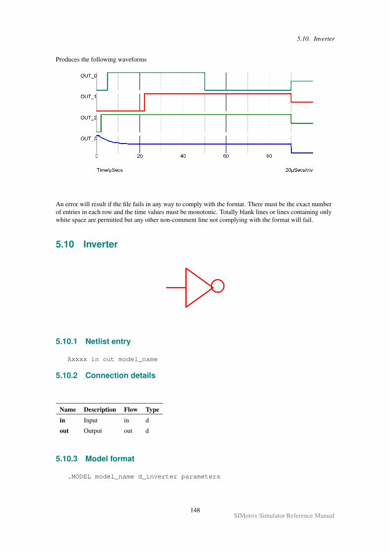
5.10. Inverter
Produces the following waveforms
An error will result if the file fails in any way to comply with the format. There must be the exact numberof entries in each row and the time values must be monotonic. Totally blank lines or lines containing onlywhite space are permitted but any other non-comment line not complying with the format will fail.
5.10 Inverter
5.10.1 Netlist entry
Axxxx in out model_name
5.10.2 Connection details
Name Description Flow Type
in Input in d
out Output out d
5.10.3 Model format
.MODEL model_name d_inverter parameters
148SIMetrix Simulator Reference Manual
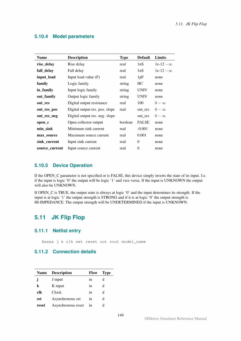
5.11. JK Flip Flop
5.10.4 Model parameters
Name Description Type Default Limits
rise_delay Rise delay real 1nS 1e-12 −∞fall_delay Fall delay real 1nS 1e-12 −∞input_load Input load value (F) real 1pF none
family Logic family string HC none
in_family Input logic family string UNIV none
out_family Output logic family string UNIV none
out_res Digital output resistance real 100 0−∞out_res_pos Digital output res. pos. slope real out_res 0−∞out_res_neg Digital output res. neg. slope out_res 0−∞open_c Open collector output boolean FALSE none
min_sink Minimum sink current real -0.001 none
max_source Maximum source current real 0.001 none
sink_current Input sink current real 0 none
source_current Input source current real 0 none
5.10.5 Device Operation
If the OPEN_C parameter is not specified or is FALSE, this device simply inverts the state of its input. I.e.if the input is logic ‘0’ the output will be logic ‘1’ and vice-versa. If the input is UNKNOWN the outputwill also be UNKNOWN.
If OPEN_C is TRUE, the output state is always at logic ‘0’ and the input determines its strength. If theinput is at logic ‘1’ the output strength is STRONG and if it is at logic ‘0’ the output strength isHI-IMPEDANCE. The output strength will be UNDETERMINED if the input is UNKNOWN.
5.11 JK Flip Flop
5.11.1 Netlist entry
Axxxx j k clk set reset out nout model_name
5.11.2 Connection details
Name Description Flow Type
j J input in d
k K input in d
clk Clock in d
set Asynchronous set in d
reset Asynchronous reset in d
149SIMetrix Simulator Reference Manual
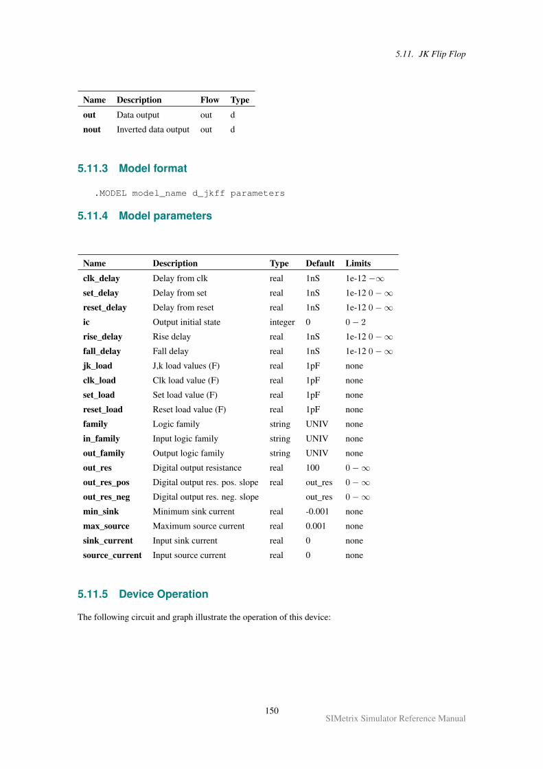
5.11. JK Flip Flop
Name Description Flow Type
out Data output out d
nout Inverted data output out d
5.11.3 Model format
.MODEL model_name d_jkff parameters
5.11.4 Model parameters
Name Description Type Default Limits
clk_delay Delay from clk real 1nS 1e-12 −∞set_delay Delay from set real 1nS 1e-12 0−∞reset_delay Delay from reset real 1nS 1e-12 0−∞ic Output initial state integer 0 0− 2
rise_delay Rise delay real 1nS 1e-12 0−∞fall_delay Fall delay real 1nS 1e-12 0−∞jk_load J,k load values (F) real 1pF none
clk_load Clk load value (F) real 1pF none
set_load Set load value (F) real 1pF none
reset_load Reset load value (F) real 1pF none
family Logic family string UNIV none
in_family Input logic family string UNIV none
out_family Output logic family string UNIV none
out_res Digital output resistance real 100 0−∞out_res_pos Digital output res. pos. slope real out_res 0−∞out_res_neg Digital output res. neg. slope out_res 0−∞min_sink Minimum sink current real -0.001 none
max_source Maximum source current real 0.001 none
sink_current Input sink current real 0 none
source_current Input source current real 0 none
5.11.5 Device Operation
The following circuit and graph illustrate the operation of this device:
150SIMetrix Simulator Reference Manual
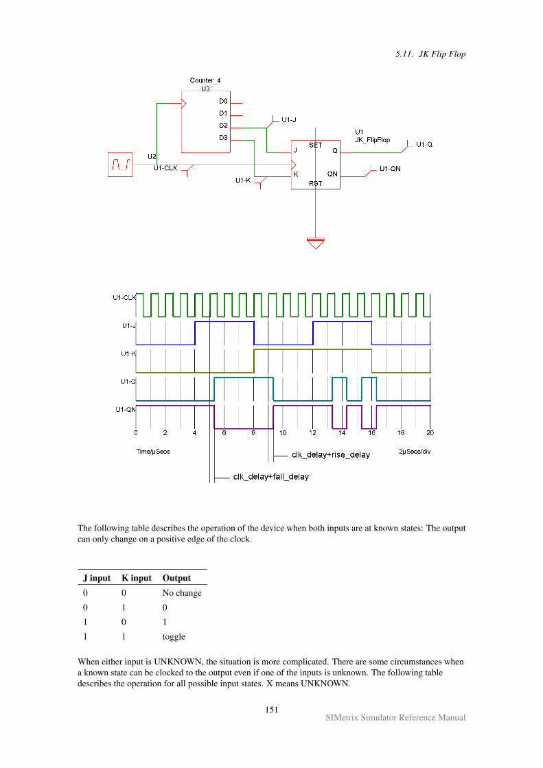
5.11. JK Flip Flop
The following table describes the operation of the device when both inputs are at known states: The outputcan only change on a positive edge of the clock.
J input K input Output
0 0 No change
0 1 0
1 0 1
1 1 toggle
When either input is UNKNOWN, the situation is more complicated. There are some circumstances whena known state can be clocked to the output even if one of the inputs is unknown. The following tabledescribes the operation for all possible input states. X means UNKNOWN.
151SIMetrix Simulator Reference Manual
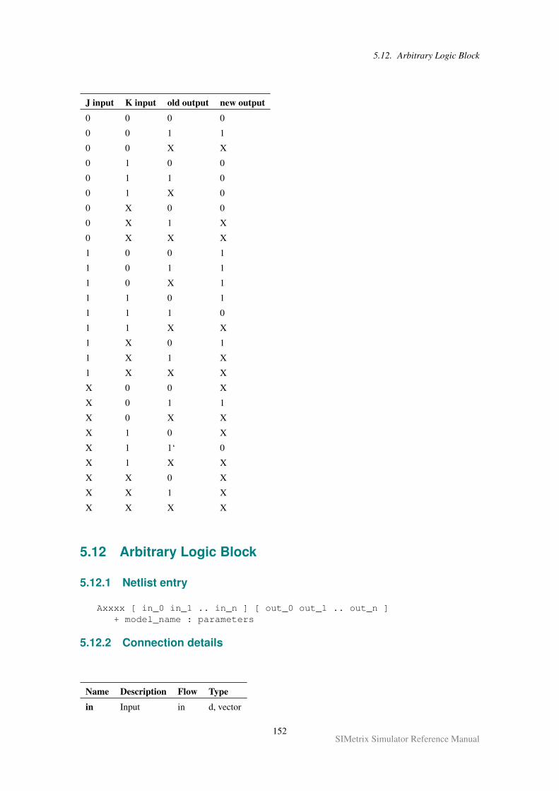
5.12. Arbitrary Logic Block
J input K input old output new output
0 0 0 0
0 0 1 1
0 0 X X
0 1 0 0
0 1 1 0
0 1 X 0
0 X 0 0
0 X 1 X
0 X X X
1 0 0 1
1 0 1 1
1 0 X 1
1 1 0 1
1 1 1 0
1 1 X X
1 X 0 1
1 X 1 X
1 X X X
X 0 0 X
X 0 1 1
X 0 X X
X 1 0 X
X 1 1‘ 0
X 1 X X
X X 0 X
X X 1 X
X X X X
5.12 Arbitrary Logic Block
5.12.1 Netlist entry
Axxxx [ in_0 in_1 .. in_n ] [ out_0 out_1 .. out_n ]+ model_name : parameters
5.12.2 Connection details
Name Description Flow Type
in Input in d, vector
152SIMetrix Simulator Reference Manual
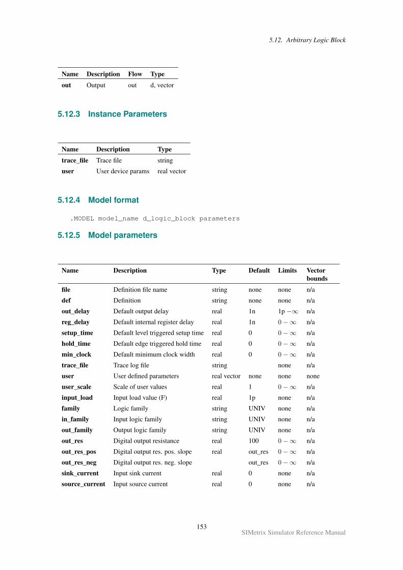
5.12. Arbitrary Logic Block
Name Description Flow Type
out Output out d, vector
5.12.3 Instance Parameters
Name Description Type
trace_file Trace file string
user User device params real vector
5.12.4 Model format
.MODEL model_name d_logic_block parameters
5.12.5 Model parameters
Name Description Type Default Limits Vectorbounds
file Definition file name string none none n/a
def Definition string none none n/a
out_delay Default output delay real 1n 1p −∞ n/a
reg_delay Default internal register delay real 1n 0−∞ n/a
setup_time Default level triggered setup time real 0 0−∞ n/a
hold_time Default edge triggered hold time real 0 0−∞ n/a
min_clock Default minimum clock width real 0 0−∞ n/a
trace_file Trace log file string none n/a
user User defined parameters real vector none none none
user_scale Scale of user values real 1 0−∞ n/a
input_load Input load value (F) real 1p none n/a
family Logic family string UNIV none n/a
in_family Input logic family string UNIV none n/a
out_family Output logic family string UNIV none n/a
out_res Digital output resistance real 100 0−∞ n/a
out_res_pos Digital output res. pos. slope real out_res 0−∞ n/a
out_res_neg Digital output res. neg. slope out_res 0−∞ n/a
sink_current Input sink current real 0 none n/a
source_current Input source current real 0 none n/a
153SIMetrix Simulator Reference Manual
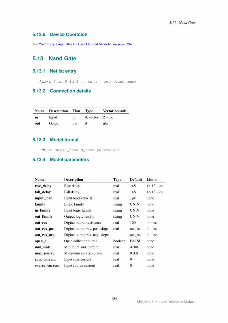
5.13. Nand Gate
5.12.6 Device Operation
See “Arbitrary Logic Block - User Defined Models” on page 294.
5.13 Nand Gate
5.13.1 Netlist entry
Axxxx [ in_0 in_1 .. in_n ] out model_name
5.13.2 Connection details
Name Description Flow Type Vector bounds
in Input in d, vector 2−∞out Output out d n/a
5.13.3 Model format
.MODEL model_name d_nand parameters
5.13.4 Model parameters
Name Description Type Default Limits
rise_delay Rise delay real 1nS 1e-12 −∞fall_delay Fall delay real 1nS 1e-12 −∞input_load Input load value (F) real 1pF none
family Logic family string UNIV none
in_family Input logic family string UNIV none
out_family Output logic family string UNIV none
out_res Digital output resistance real 100 0−∞out_res_pos Digital output res. pos. slope real out_res 0−∞out_res_neg Digital output res. neg. slope out_res 0−∞open_c Open collector output boolean FALSE none
min_sink Minimum sink current real -0.001 none
max_source Maximum source current real 0.001 none
sink_current Input sink current real 0 none
source_current Input source current real 0 none
154SIMetrix Simulator Reference Manual
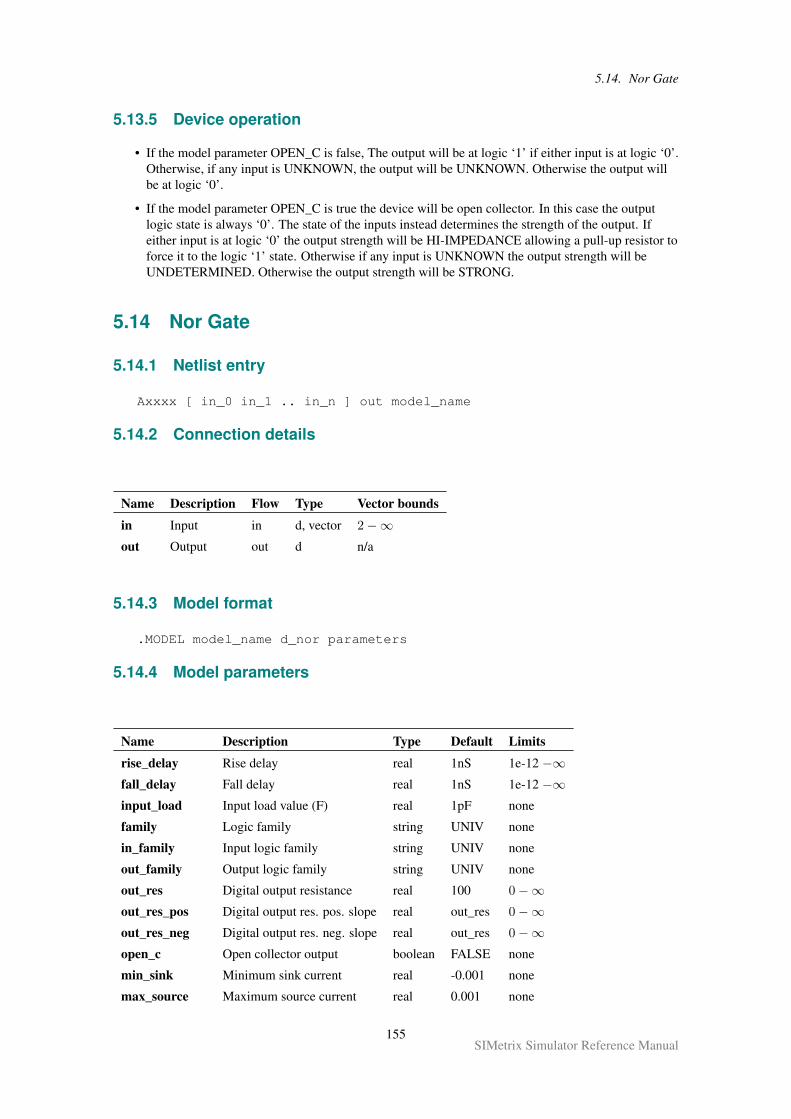
5.14. Nor Gate
5.13.5 Device operation
• If the model parameter OPEN_C is false, The output will be at logic ‘1’ if either input is at logic ‘0’.Otherwise, if any input is UNKNOWN, the output will be UNKNOWN. Otherwise the output willbe at logic ‘0’.
• If the model parameter OPEN_C is true the device will be open collector. In this case the outputlogic state is always ‘0’. The state of the inputs instead determines the strength of the output. Ifeither input is at logic ‘0’ the output strength will be HI-IMPEDANCE allowing a pull-up resistor toforce it to the logic ‘1’ state. Otherwise if any input is UNKNOWN the output strength will beUNDETERMINED. Otherwise the output strength will be STRONG.
5.14 Nor Gate
5.14.1 Netlist entry
Axxxx [ in_0 in_1 .. in_n ] out model_name
5.14.2 Connection details
Name Description Flow Type Vector bounds
in Input in d, vector 2−∞out Output out d n/a
5.14.3 Model format
.MODEL model_name d_nor parameters
5.14.4 Model parameters
Name Description Type Default Limits
rise_delay Rise delay real 1nS 1e-12 −∞fall_delay Fall delay real 1nS 1e-12 −∞input_load Input load value (F) real 1pF none
family Logic family string UNIV none
in_family Input logic family string UNIV none
out_family Output logic family string UNIV none
out_res Digital output resistance real 100 0−∞out_res_pos Digital output res. pos. slope real out_res 0−∞out_res_neg Digital output res. neg. slope real out_res 0−∞open_c Open collector output boolean FALSE none
min_sink Minimum sink current real -0.001 none
max_source Maximum source current real 0.001 none
155SIMetrix Simulator Reference Manual
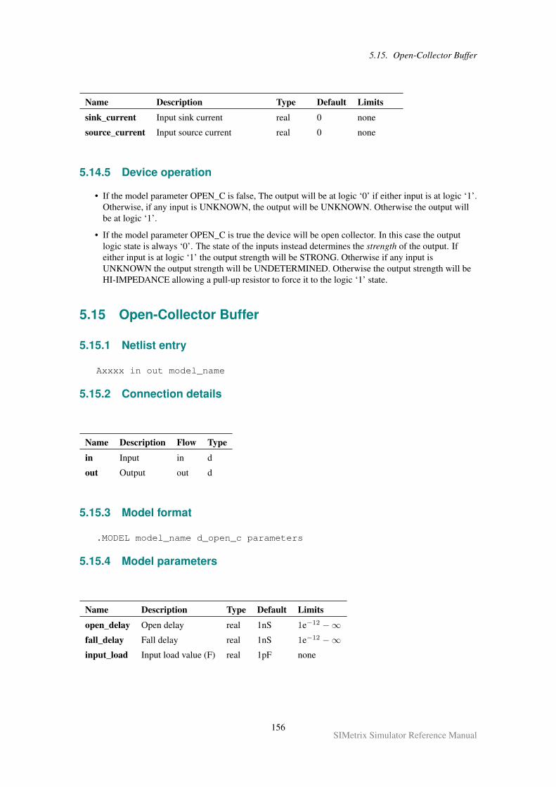
5.15. Open-Collector Buffer
Name Description Type Default Limits
sink_current Input sink current real 0 none
source_current Input source current real 0 none
5.14.5 Device operation
• If the model parameter OPEN_C is false, The output will be at logic ‘0’ if either input is at logic ‘1’.Otherwise, if any input is UNKNOWN, the output will be UNKNOWN. Otherwise the output willbe at logic ‘1’.
• If the model parameter OPEN_C is true the device will be open collector. In this case the outputlogic state is always ‘0’. The state of the inputs instead determines the strength of the output. Ifeither input is at logic ‘1’ the output strength will be STRONG. Otherwise if any input isUNKNOWN the output strength will be UNDETERMINED. Otherwise the output strength will beHI-IMPEDANCE allowing a pull-up resistor to force it to the logic ‘1’ state.
5.15 Open-Collector Buffer
5.15.1 Netlist entry
Axxxx in out model_name
5.15.2 Connection details
Name Description Flow Type
in Input in d
out Output out d
5.15.3 Model format
.MODEL model_name d_open_c parameters
5.15.4 Model parameters
Name Description Type Default Limits
open_delay Open delay real 1nS 1e−12 −∞fall_delay Fall delay real 1nS 1e−12 −∞input_load Input load value (F) real 1pF none
156SIMetrix Simulator Reference Manual
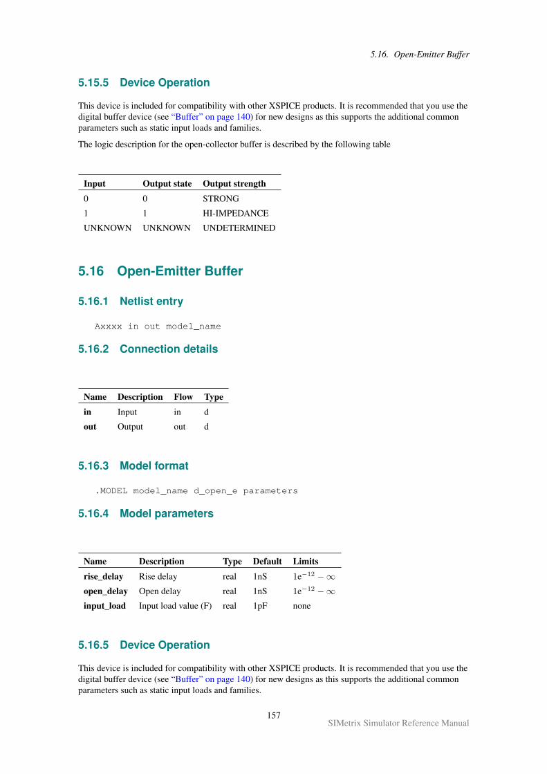
5.16. Open-Emitter Buffer
5.15.5 Device Operation
This device is included for compatibility with other XSPICE products. It is recommended that you use thedigital buffer device (see “Buffer” on page 140) for new designs as this supports the additional commonparameters such as static input loads and families.
The logic description for the open-collector buffer is described by the following table
Input Output state Output strength
0 0 STRONG
1 1 HI-IMPEDANCE
UNKNOWN UNKNOWN UNDETERMINED
5.16 Open-Emitter Buffer
5.16.1 Netlist entry
Axxxx in out model_name
5.16.2 Connection details
Name Description Flow Type
in Input in d
out Output out d
5.16.3 Model format
.MODEL model_name d_open_e parameters
5.16.4 Model parameters
Name Description Type Default Limits
rise_delay Rise delay real 1nS 1e−12 −∞open_delay Open delay real 1nS 1e−12 −∞input_load Input load value (F) real 1pF none
5.16.5 Device Operation
This device is included for compatibility with other XSPICE products. It is recommended that you use thedigital buffer device (see “Buffer” on page 140) for new designs as this supports the additional commonparameters such as static input loads and families.
157SIMetrix Simulator Reference Manual
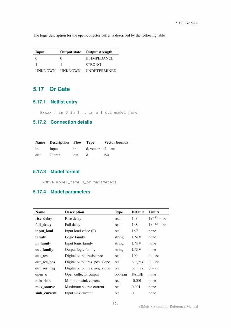
5.17. Or Gate
The logic description for the open-collector buffer is described by the following table
Input Output state Output strength
0 0 HI-IMPEDANCE
1 1 STRONG
UNKNOWN UNKNOWN UNDETERMINED
5.17 Or Gate
5.17.1 Netlist entry
Axxxx [ in_0 in_1 .. in_n ] out model_name
5.17.2 Connection details
Name Description Flow Type Vector bounds
in Input in d, vector 2−∞out Output out d n/a
5.17.3 Model format
.MODEL model_name d_or parameters
5.17.4 Model parameters
Name Description Type Default Limits
rise_delay Rise delay real 1nS 1e−12 −∞fall_delay Fall delay real 1nS 1e−12 −∞input_load Input load value (F) real 1pF none
family Logic family string UNIV none
in_family Input logic family string UNIV none
out_family Output logic family string UNIV none
out_res Digital output resistance real 100 0−∞out_res_pos Digital output res. pos. slope real out_res 0−∞out_res_neg Digital output res. neg. slope real out_res 0−∞open_c Open collector output boolean FALSE none
min_sink Minimum sink current real -0.001 none
max_source Maximum source current real 0.001 none
sink_current Input sink current real 0 none
158SIMetrix Simulator Reference Manual
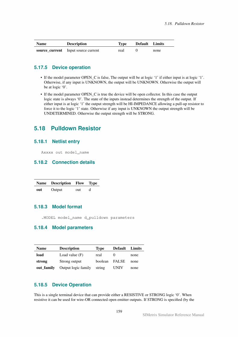
5.18. Pulldown Resistor
Name Description Type Default Limits
source_current Input source current real 0 none
5.17.5 Device operation
• If the model parameter OPEN_C is false, The output will be at logic ‘1’ if either input is at logic ‘1’.Otherwise, if any input is UNKNOWN, the output will be UNKNOWN. Otherwise the output willbe at logic ‘0’.
• If the model parameter OPEN_C is true the device will be open collector. In this case the outputlogic state is always ‘0’. The state of the inputs instead determines the strength of the output. Ifeither input is at logic ‘1’ the output strength will be HI-IMPEDANCE allowing a pull-up resistor toforce it to the logic ‘1’ state. Otherwise if any input is UNKNOWN the output strength will beUNDETERMINED. Otherwise the output strength will be STRONG.
5.18 Pulldown Resistor
5.18.1 Netlist entry
Axxxx out model_name
5.18.2 Connection details
Name Description Flow Type
out Output out d
5.18.3 Model format
.MODEL model_name d_pulldown parameters
5.18.4 Model parameters
Name Description Type Default Limits
load Load value (F) real 0 none
strong Strong output boolean FALSE none
out_family Output logic family string UNIV none
5.18.5 Device Operation
This is a single terminal device that can provide either a RESISTIVE or STRONG logic ‘0’. Whenresistive it can be used for wire-OR connected open emitter outputs. If STRONG is specified (by the
159SIMetrix Simulator Reference Manual
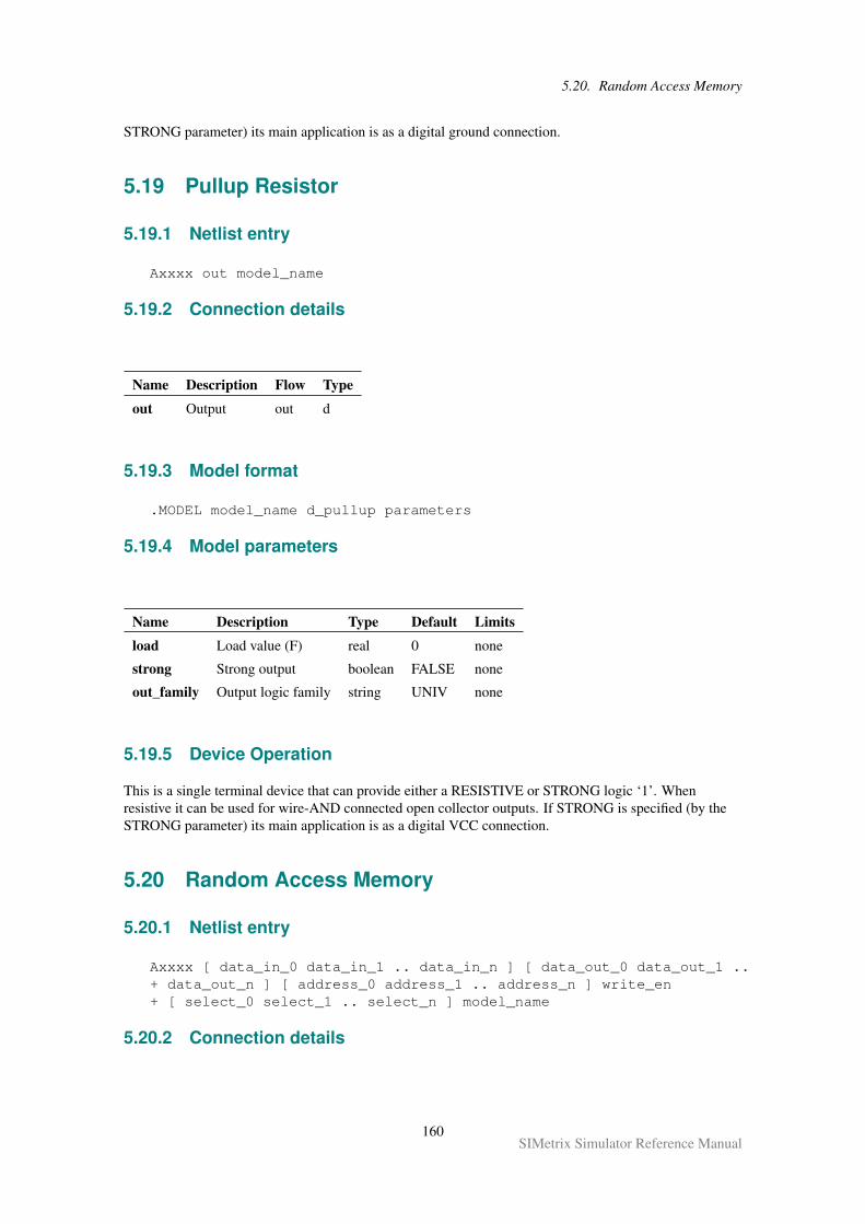
5.20. Random Access Memory
STRONG parameter) its main application is as a digital ground connection.
5.19 Pullup Resistor
5.19.1 Netlist entry
Axxxx out model_name
5.19.2 Connection details
Name Description Flow Type
out Output out d
5.19.3 Model format
.MODEL model_name d_pullup parameters
5.19.4 Model parameters
Name Description Type Default Limits
load Load value (F) real 0 none
strong Strong output boolean FALSE none
out_family Output logic family string UNIV none
5.19.5 Device Operation
This is a single terminal device that can provide either a RESISTIVE or STRONG logic ‘1’. Whenresistive it can be used for wire-AND connected open collector outputs. If STRONG is specified (by theSTRONG parameter) its main application is as a digital VCC connection.
5.20 Random Access Memory
5.20.1 Netlist entry
Axxxx [ data_in_0 data_in_1 .. data_in_n ] [ data_out_0 data_out_1 ..+ data_out_n ] [ address_0 address_1 .. address_n ] write_en+ [ select_0 select_1 .. select_n ] model_name
5.20.2 Connection details
160SIMetrix Simulator Reference Manual
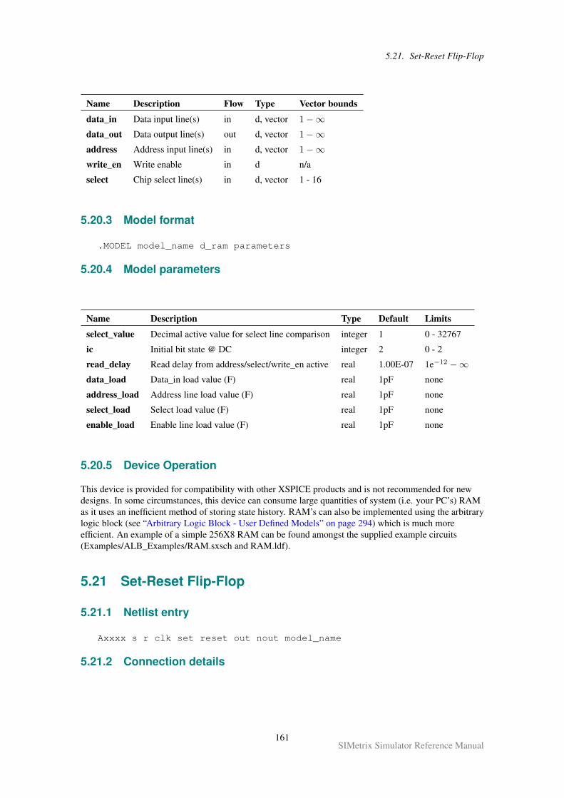
5.21. Set-Reset Flip-Flop
Name Description Flow Type Vector bounds
data_in Data input line(s) in d, vector 1−∞data_out Data output line(s) out d, vector 1−∞address Address input line(s) in d, vector 1−∞write_en Write enable in d n/a
select Chip select line(s) in d, vector 1 - 16
5.20.3 Model format
.MODEL model_name d_ram parameters
5.20.4 Model parameters
Name Description Type Default Limits
select_value Decimal active value for select line comparison integer 1 0 - 32767
ic Initial bit state @ DC integer 2 0 - 2
read_delay Read delay from address/select/write_en active real 1.00E-07 1e−12 −∞data_load Data_in load value (F) real 1pF none
address_load Address line load value (F) real 1pF none
select_load Select load value (F) real 1pF none
enable_load Enable line load value (F) real 1pF none
5.20.5 Device Operation
This device is provided for compatibility with other XSPICE products and is not recommended for newdesigns. In some circumstances, this device can consume large quantities of system (i.e. your PC’s) RAMas it uses an inefficient method of storing state history. RAM’s can also be implemented using the arbitrarylogic block (see “Arbitrary Logic Block - User Defined Models” on page 294) which is much moreefficient. An example of a simple 256X8 RAM can be found amongst the supplied example circuits(Examples/ALB_Examples/RAM.sxsch and RAM.ldf).
5.21 Set-Reset Flip-Flop
5.21.1 Netlist entry
Axxxx s r clk set reset out nout model_name
5.21.2 Connection details
161SIMetrix Simulator Reference Manual
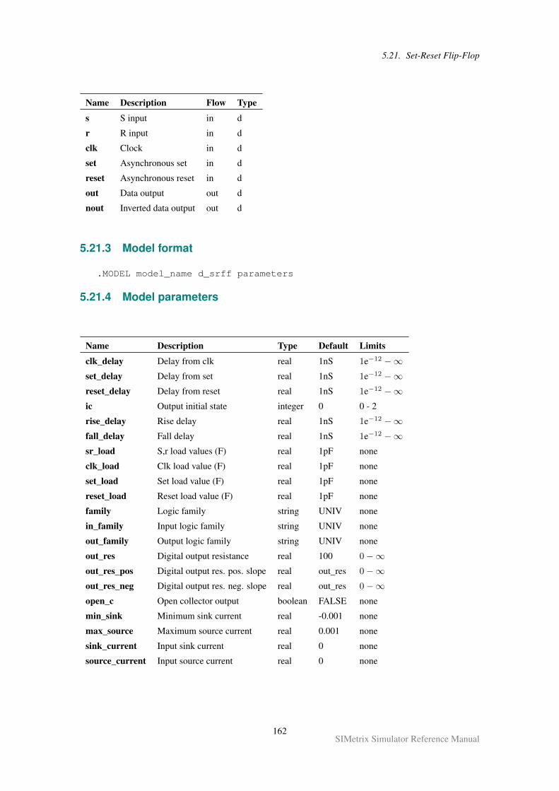
5.21. Set-Reset Flip-Flop
Name Description Flow Type
s S input in d
r R input in d
clk Clock in d
set Asynchronous set in d
reset Asynchronous reset in d
out Data output out d
nout Inverted data output out d
5.21.3 Model format
.MODEL model_name d_srff parameters
5.21.4 Model parameters
Name Description Type Default Limits
clk_delay Delay from clk real 1nS 1e−12 −∞set_delay Delay from set real 1nS 1e−12 −∞reset_delay Delay from reset real 1nS 1e−12 −∞ic Output initial state integer 0 0 - 2
rise_delay Rise delay real 1nS 1e−12 −∞fall_delay Fall delay real 1nS 1e−12 −∞sr_load S,r load values (F) real 1pF none
clk_load Clk load value (F) real 1pF none
set_load Set load value (F) real 1pF none
reset_load Reset load value (F) real 1pF none
family Logic family string UNIV none
in_family Input logic family string UNIV none
out_family Output logic family string UNIV none
out_res Digital output resistance real 100 0−∞out_res_pos Digital output res. pos. slope real out_res 0−∞out_res_neg Digital output res. neg. slope real out_res 0−∞open_c Open collector output boolean FALSE none
min_sink Minimum sink current real -0.001 none
max_source Maximum source current real 0.001 none
sink_current Input sink current real 0 none
source_current Input source current real 0 none
162SIMetrix Simulator Reference Manual
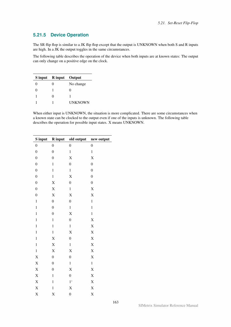
5.21. Set-Reset Flip-Flop
5.21.5 Device Operation
The SR flip flop is similar to a JK flip flop except that the output is UNKNOWN when both S and R inputsare high. In a JK the output toggles in the same circumstances.
The following table describes the operation of the device when both inputs are at known states: The outputcan only change on a positive edge on the clock.
S input R input Output
0 0 No change
0 1 0
1 0 1
1 1 UNKNOWN
When either input is UNKNOWN, the situation is more complicated. There are some circumstances whena known state can be clocked to the output even if one of the inputs is unknown. The following tabledescribes the operation for possible input states. X means UNKNOWN.
S input R input old output new output
0 0 0 0
0 0 1 1
0 0 X X
0 1 0 0
0 1 1 0
0 1 X 0
0 X 0 0
0 X 1 X
0 X X X
1 0 0 1
1 0 1 1
1 0 X 1
1 1 0 X
1 1 1 X
1 1 X X
1 X 0 X
1 X 1 X
1 X X X
X 0 0 X
X 0 1 1
X 0 X X
X 1 0 X
X 1 1‘ X
X 1 X X
X X 0 X
163SIMetrix Simulator Reference Manual
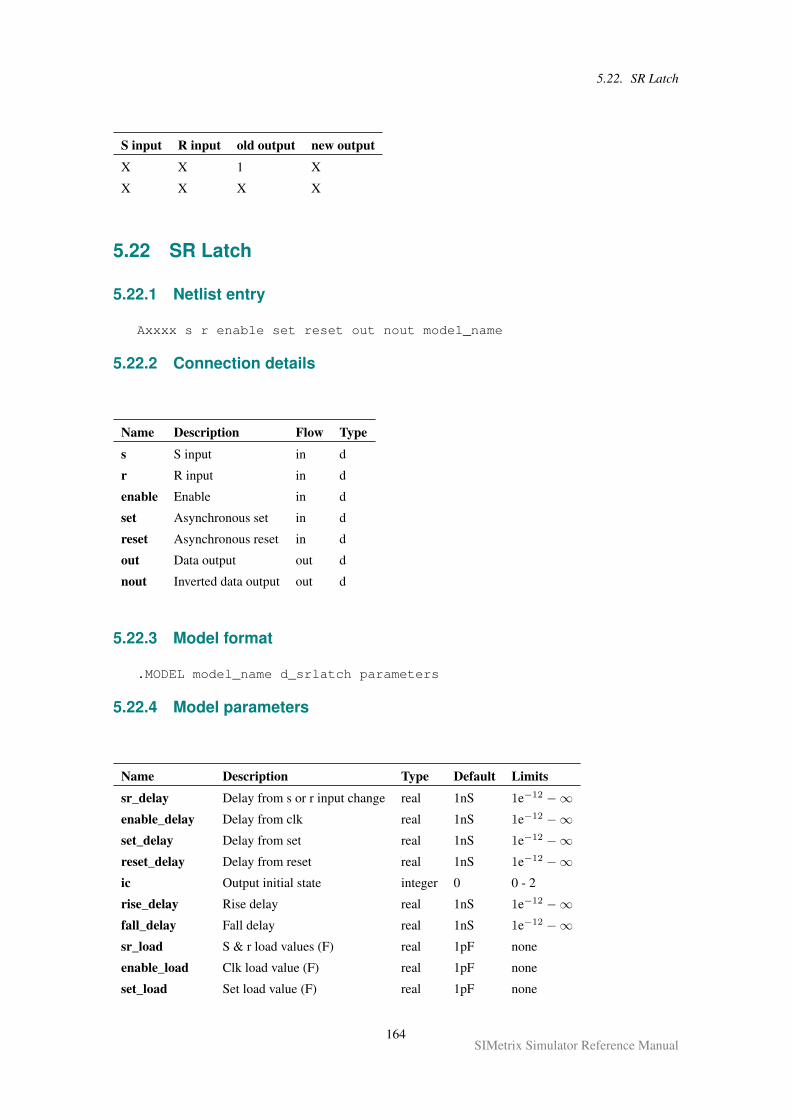
5.22. SR Latch
S input R input old output new output
X X 1 X
X X X X
5.22 SR Latch
5.22.1 Netlist entry
Axxxx s r enable set reset out nout model_name
5.22.2 Connection details
Name Description Flow Type
s S input in d
r R input in d
enable Enable in d
set Asynchronous set in d
reset Asynchronous reset in d
out Data output out d
nout Inverted data output out d
5.22.3 Model format
.MODEL model_name d_srlatch parameters
5.22.4 Model parameters
Name Description Type Default Limits
sr_delay Delay from s or r input change real 1nS 1e−12 −∞enable_delay Delay from clk real 1nS 1e−12 −∞set_delay Delay from set real 1nS 1e−12 −∞reset_delay Delay from reset real 1nS 1e−12 −∞ic Output initial state integer 0 0 - 2
rise_delay Rise delay real 1nS 1e−12 −∞fall_delay Fall delay real 1nS 1e−12 −∞sr_load S & r load values (F) real 1pF none
enable_load Clk load value (F) real 1pF none
set_load Set load value (F) real 1pF none
164SIMetrix Simulator Reference Manual
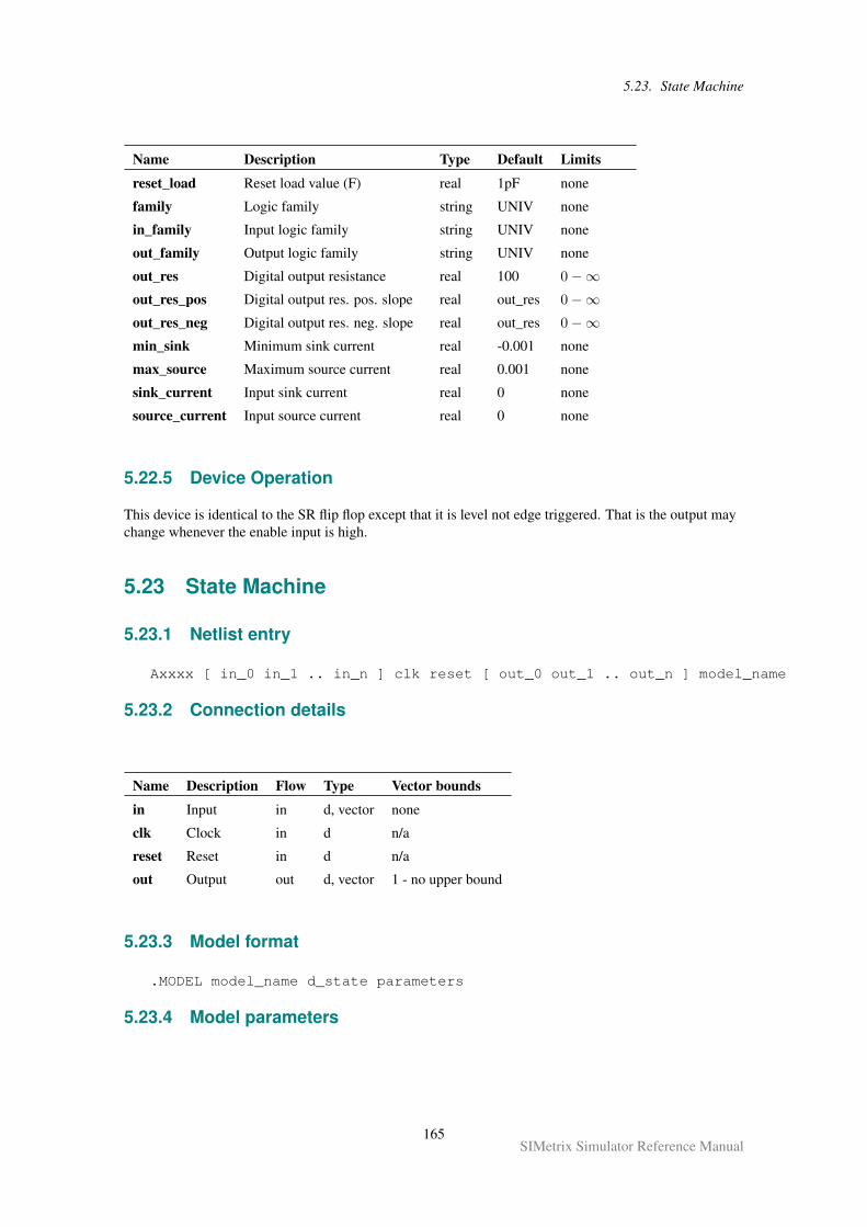
5.23. State Machine
Name Description Type Default Limits
reset_load Reset load value (F) real 1pF none
family Logic family string UNIV none
in_family Input logic family string UNIV none
out_family Output logic family string UNIV none
out_res Digital output resistance real 100 0−∞out_res_pos Digital output res. pos. slope real out_res 0−∞out_res_neg Digital output res. neg. slope real out_res 0−∞min_sink Minimum sink current real -0.001 none
max_source Maximum source current real 0.001 none
sink_current Input sink current real 0 none
source_current Input source current real 0 none
5.22.5 Device Operation
This device is identical to the SR flip flop except that it is level not edge triggered. That is the output maychange whenever the enable input is high.
5.23 State Machine
5.23.1 Netlist entry
Axxxx [ in_0 in_1 .. in_n ] clk reset [ out_0 out_1 .. out_n ] model_name
5.23.2 Connection details
Name Description Flow Type Vector bounds
in Input in d, vector none
clk Clock in d n/a
reset Reset in d n/a
out Output out d, vector 1 - no upper bound
5.23.3 Model format
.MODEL model_name d_state parameters
5.23.4 Model parameters
165SIMetrix Simulator Reference Manual
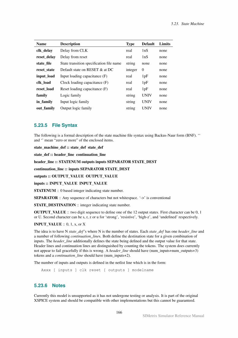
5.23. State Machine
Name Description Type Default Limits
clk_delay Delay from CLK real 1nS none
reset_delay Delay from reset real 1nS none
state_file State transition specification file name string none none
reset_state Default state on RESET & at DC integer 0 none
input_load Input loading capacitance (F) real 1pF none
clk_load Clock loading capacitance (F) real 1pF none
reset_load Reset loading capacitance (F) real 1pF none
family Logic family string UNIV none
in_family Input logic family string UNIV none
out_family Output logic family string UNIV none
5.23.5 File Syntax
The following is a formal description of the state machine file syntax using Backus-Naur form (BNF). ‘‘and ‘’ mean “zero or more” of the enclosed items.
state_machine_def :: state_def state_def
state_def :: header_line continuation_line
header_line :: STATENUM outputs inputs SEPARATOR STATE_DEST
continuation_line :: inputs SEPARATOR STATE_DEST
outputs :: OUTPUT_VALUE OUTPUT_VALUE
inputs :: INPUT_VALUE INPUT_VALUE
STATENUM :: 0 based integer indicating state number.
SEPARATOR :: Any sequence of characters but not whitespace. ‘->’ is conventional
STATE_DESTINATION :: integer indicating state number.
OUTPUT_VALUE :: two digit sequence to define one of the 12 output states. First character can be 0, 1or U. Second character can be s, r, z or u for ‘strong’, ‘resistive’, ‘high-z’, and ‘undefined’ respectively.
INPUT_VALUE :: 0, 1, x, or X
The idea is to have N state_def ’s where N is the number of states. Each state_def has one header_line anda number of following continuation_lines. Both define the destination state for a given combination ofinputs. The header_line additionally defines the state being defined and the output value for that state.Header lines and continuation lines are distinguished by counting the tokens. The system does currentlynot appear to fail gracefully if this is wrong. A header_line should have (num_inputs+num_outputs+3)tokens and a continuation_line should have (num_inputs+2).
The number of inputs and outputs is defined in the netlist line which is in the form:
Axxx [ inputs ] clk reset [ outputs ] modelname
5.23.6 Notes
Currently this model is unsupported as it has not undergone testing or analysis. It is part of the originalXSPICE system and should be compatible with other implementations but this cannot be guaranteed.
166SIMetrix Simulator Reference Manual
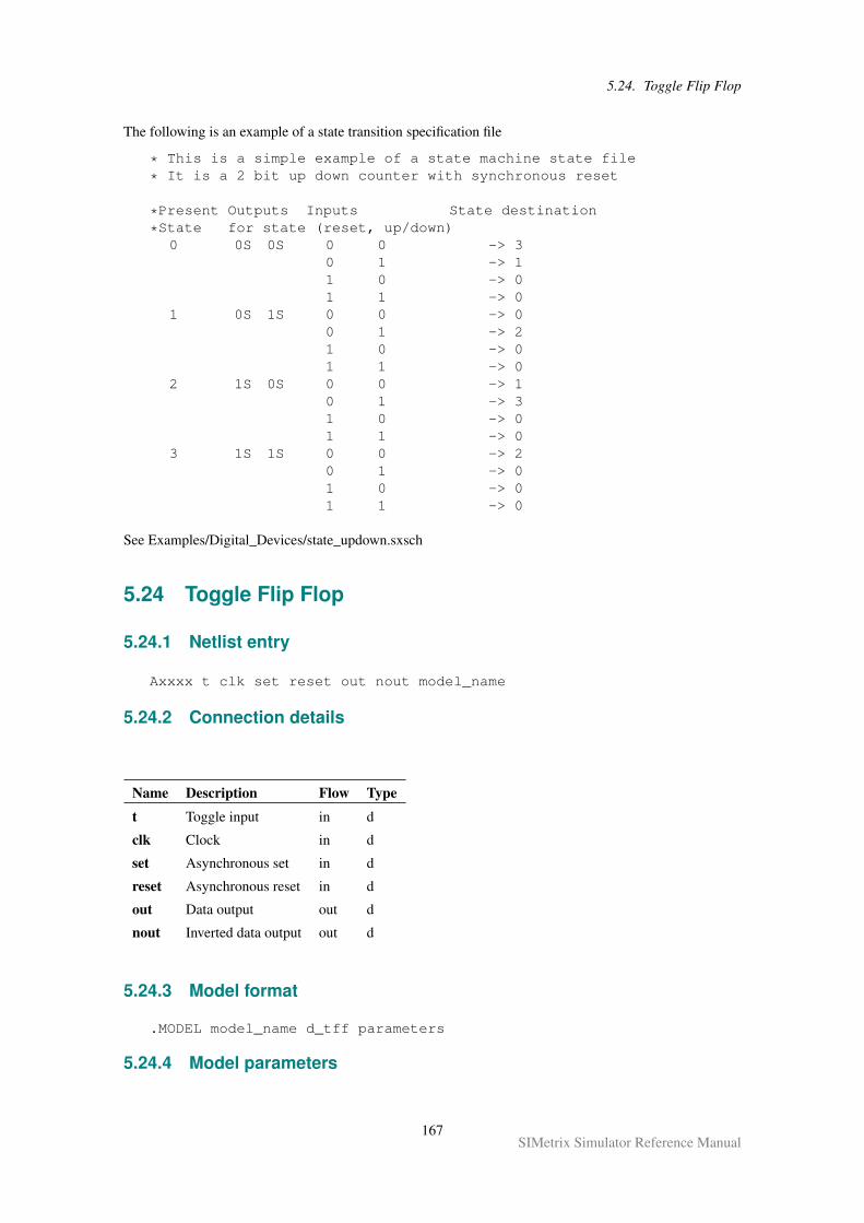
5.24. Toggle Flip Flop
The following is an example of a state transition specification file
* This is a simple example of a state machine state file
* It is a 2 bit up down counter with synchronous reset
*Present Outputs Inputs State destination
*State for state (reset, up/down)0 0S 0S 0 0 -> 3
0 1 -> 11 0 -> 01 1 -> 0
1 0S 1S 0 0 -> 00 1 -> 21 0 -> 01 1 -> 0
2 1S 0S 0 0 -> 10 1 -> 31 0 -> 01 1 -> 0
3 1S 1S 0 0 -> 20 1 -> 01 0 -> 01 1 -> 0
See Examples/Digital_Devices/state_updown.sxsch
5.24 Toggle Flip Flop
5.24.1 Netlist entry
Axxxx t clk set reset out nout model_name
5.24.2 Connection details
Name Description Flow Type
t Toggle input in d
clk Clock in d
set Asynchronous set in d
reset Asynchronous reset in d
out Data output out d
nout Inverted data output out d
5.24.3 Model format
.MODEL model_name d_tff parameters
5.24.4 Model parameters
167SIMetrix Simulator Reference Manual
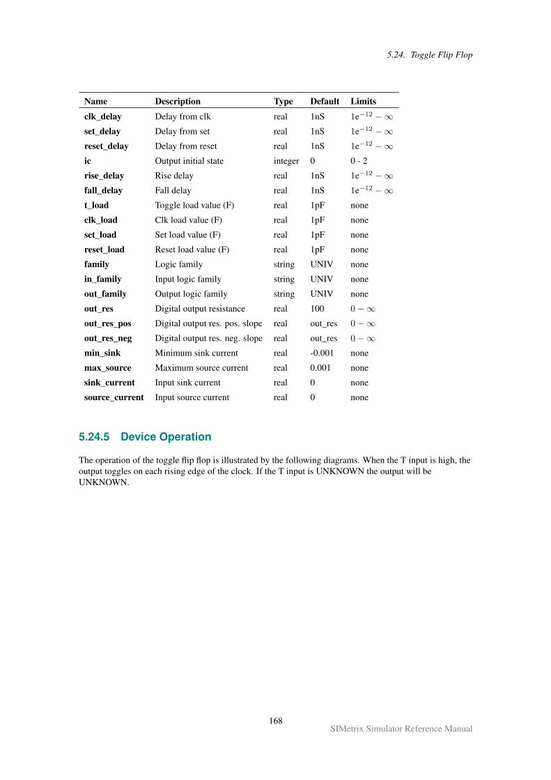
5.24. Toggle Flip Flop
Name Description Type Default Limits
clk_delay Delay from clk real 1nS 1e−12 −∞set_delay Delay from set real 1nS 1e−12 −∞reset_delay Delay from reset real 1nS 1e−12 −∞ic Output initial state integer 0 0 - 2
rise_delay Rise delay real 1nS 1e−12 −∞fall_delay Fall delay real 1nS 1e−12 −∞t_load Toggle load value (F) real 1pF none
clk_load Clk load value (F) real 1pF none
set_load Set load value (F) real 1pF none
reset_load Reset load value (F) real 1pF none
family Logic family string UNIV none
in_family Input logic family string UNIV none
out_family Output logic family string UNIV none
out_res Digital output resistance real 100 0−∞out_res_pos Digital output res. pos. slope real out_res 0−∞out_res_neg Digital output res. neg. slope real out_res 0−∞min_sink Minimum sink current real -0.001 none
max_source Maximum source current real 0.001 none
sink_current Input sink current real 0 none
source_current Input source current real 0 none
5.24.5 Device Operation
The operation of the toggle flip flop is illustrated by the following diagrams. When the T input is high, theoutput toggles on each rising edge of the clock. If the T input is UNKNOWN the output will beUNKNOWN.
168SIMetrix Simulator Reference Manual
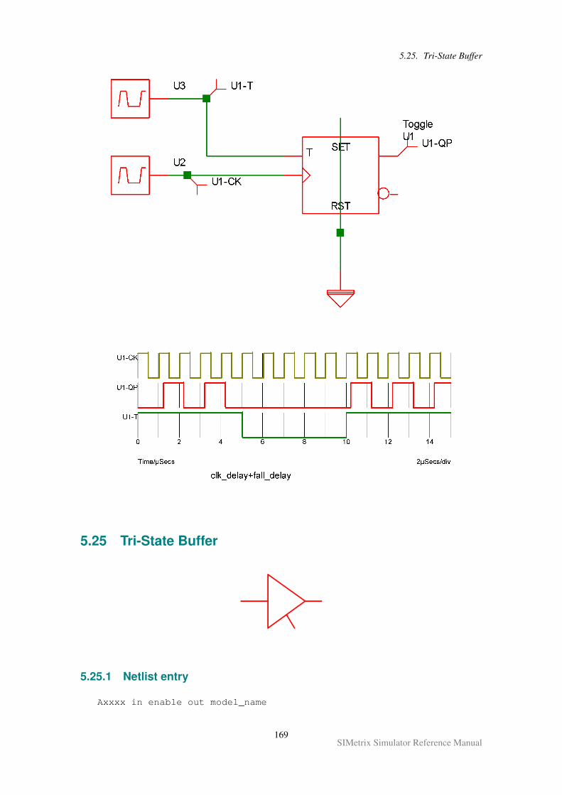
5.25. Tri-State Buffer
5.25 Tri-State Buffer
5.25.1 Netlist entry
Axxxx in enable out model_name
169SIMetrix Simulator Reference Manual
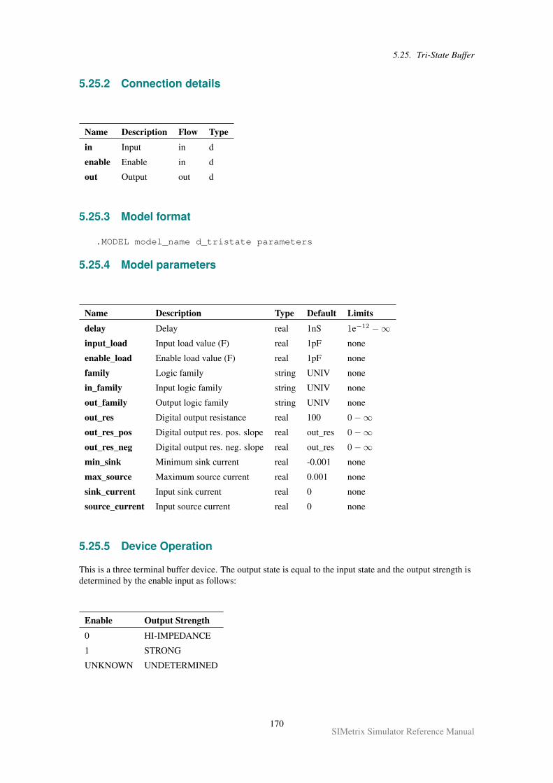
5.25. Tri-State Buffer
5.25.2 Connection details
Name Description Flow Type
in Input in d
enable Enable in d
out Output out d
5.25.3 Model format
.MODEL model_name d_tristate parameters
5.25.4 Model parameters
Name Description Type Default Limits
delay Delay real 1nS 1e−12 −∞input_load Input load value (F) real 1pF none
enable_load Enable load value (F) real 1pF none
family Logic family string UNIV none
in_family Input logic family string UNIV none
out_family Output logic family string UNIV none
out_res Digital output resistance real 100 0−∞out_res_pos Digital output res. pos. slope real out_res 0−∞out_res_neg Digital output res. neg. slope real out_res 0−∞min_sink Minimum sink current real -0.001 none
max_source Maximum source current real 0.001 none
sink_current Input sink current real 0 none
source_current Input source current real 0 none
5.25.5 Device Operation
This is a three terminal buffer device. The output state is equal to the input state and the output strength isdetermined by the enable input as follows:
Enable Output Strength
0 HI-IMPEDANCE
1 STRONG
UNKNOWN UNDETERMINED
170SIMetrix Simulator Reference Manual
5.26. Exclusive NOR Gate
5.26 Exclusive NOR Gate
5.26.1 Netlist entry
Axxxx [ in_0 in_1 .. in_n ] out model_name
5.26.2 Connection details
Name Description Flow Type Vector bounds
in Input in d, vector 2−∞out Output out d n/a
5.26.3 Model format
.MODEL model_name d_xnor parameters
5.26.4 Model parameters
Name Description Type Default Limits
rise_delay Rise delay real 1nS 1e−12 −∞fall_delay Fall delay real 1nS 1e−12 −∞input_load Input load value (pF) real 1 0−∞family Logic family string UNIV none
in_family Input logic family string UNIV none
out_family Output logic family string UNIV none
out_res Digital output resistance real 100 0−∞out_res_pos Digital output res. pos. slope real out_res 0−∞out_res_neg Digital output res. neg. slope real out_res 0−∞open_c Open collector output boolean FALSE none
min_sink Minimum sink current real -0.001 none
max_source Maximum source current real 0.001 none
sink_current Input sink current real 0 none
source_current Input source current real 0 none
5.26.5 Device Operation
• If the OPEN_C parameter is FALSE, the output is at logic ‘1’ if an even number of inputs are atlogic ‘1’. If any input is UNKNOWN the output will be UNKNOWN, otherwise the output will beat logic ‘0’.
• If the model parameter OPEN_C is true the device will be open collector. In this case the outputlogic state is always ‘0’. The state of the inputs instead determines the strength of the output. If n
171SIMetrix Simulator Reference Manual
5.27. Exclusive OR Gate
even number of inputs are at logic ‘1’ the output strength will be HI-IMPEDANCE allowing apull-up resistor to force it to the logic ‘1’ state. If any input is UNKNOWN the output strength willbe UNDETERMINED. Otherwise the output strength will be STRONG.
5.27 Exclusive OR Gate
5.27.1 Netlist entry
Axxxx [ in_0 in_1 .. in_n ] out model_name
5.27.2 Connection details
Name Description Flow Type Vector bounds
in Input in d, vector 2−∞out Output out d n/a
5.27.3 Model format
.MODEL model_name d_xor parameters
5.27.4 Model parameters
Name Description Type Default Limits
rise_delay Rise delay real 1nS 1e−12 −∞fall_delay Fall delay real 1nS 1e−12 −∞input_load Input load value (F) real 1pF none
family Logic family string UNIV none
in_family Input logic family string UNIV none
out_family Output logic family string UNIV none
out_res Digital output resistance real 100 0−∞out_res_pos Digital output res. pos. slope real out_res 0−∞out_res_neg Digital output res. neg. slope real out_res 0−∞open_c Open collector output boolean FALSE none
min_sink Minimum sink current real -0.001 none
max_source Maximum source current real 0.001 none
sink_current Input sink current real 0 none
source_current Input source current real 0 none
172SIMetrix Simulator Reference Manual
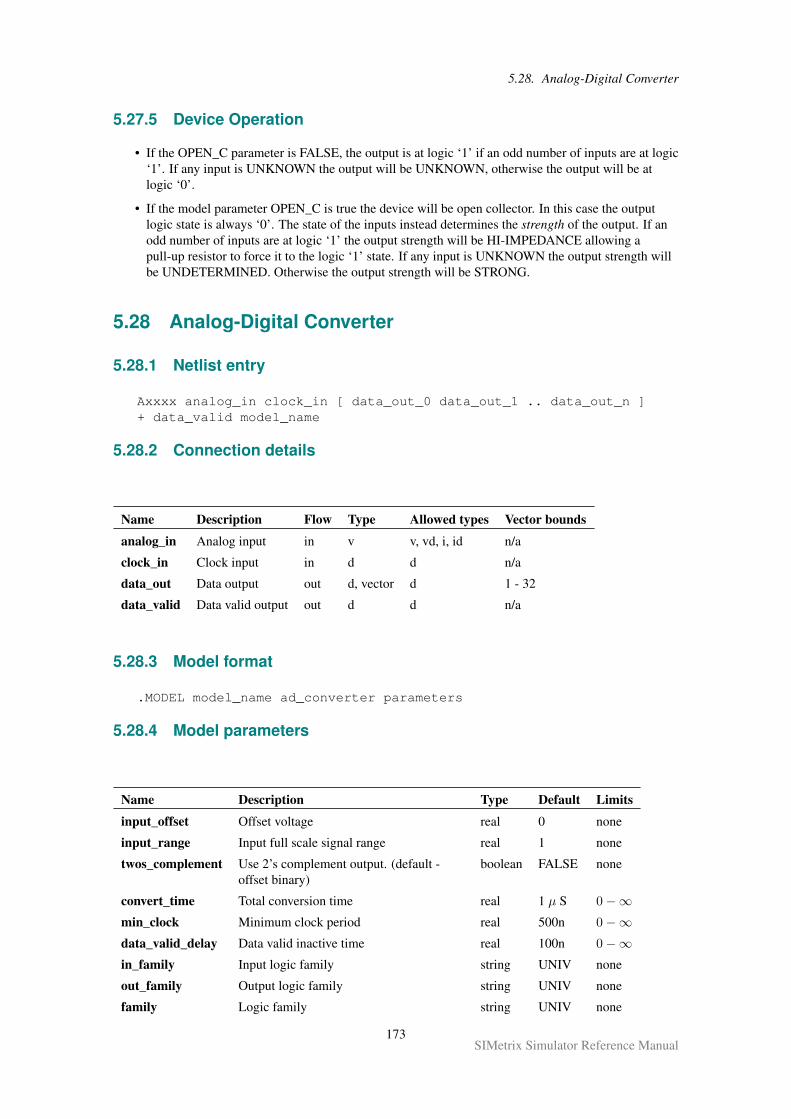
5.28. Analog-Digital Converter
5.27.5 Device Operation
• If the OPEN_C parameter is FALSE, the output is at logic ‘1’ if an odd number of inputs are at logic‘1’. If any input is UNKNOWN the output will be UNKNOWN, otherwise the output will be atlogic ‘0’.
• If the model parameter OPEN_C is true the device will be open collector. In this case the outputlogic state is always ‘0’. The state of the inputs instead determines the strength of the output. If anodd number of inputs are at logic ‘1’ the output strength will be HI-IMPEDANCE allowing apull-up resistor to force it to the logic ‘1’ state. If any input is UNKNOWN the output strength willbe UNDETERMINED. Otherwise the output strength will be STRONG.
5.28 Analog-Digital Converter
5.28.1 Netlist entry
Axxxx analog_in clock_in [ data_out_0 data_out_1 .. data_out_n ]+ data_valid model_name
5.28.2 Connection details
Name Description Flow Type Allowed types Vector bounds
analog_in Analog input in v v, vd, i, id n/a
clock_in Clock input in d d n/a
data_out Data output out d, vector d 1 - 32
data_valid Data valid output out d d n/a
5.28.3 Model format
.MODEL model_name ad_converter parameters
5.28.4 Model parameters
Name Description Type Default Limits
input_offset Offset voltage real 0 none
input_range Input full scale signal range real 1 none
twos_complement Use 2’s complement output. (default -offset binary)
boolean FALSE none
convert_time Total conversion time real 1 µ S 0−∞min_clock Minimum clock period real 500n 0−∞data_valid_delay Data valid inactive time real 100n 0−∞in_family Input logic family string UNIV none
out_family Output logic family string UNIV none
family Logic family string UNIV none
173SIMetrix Simulator Reference Manual
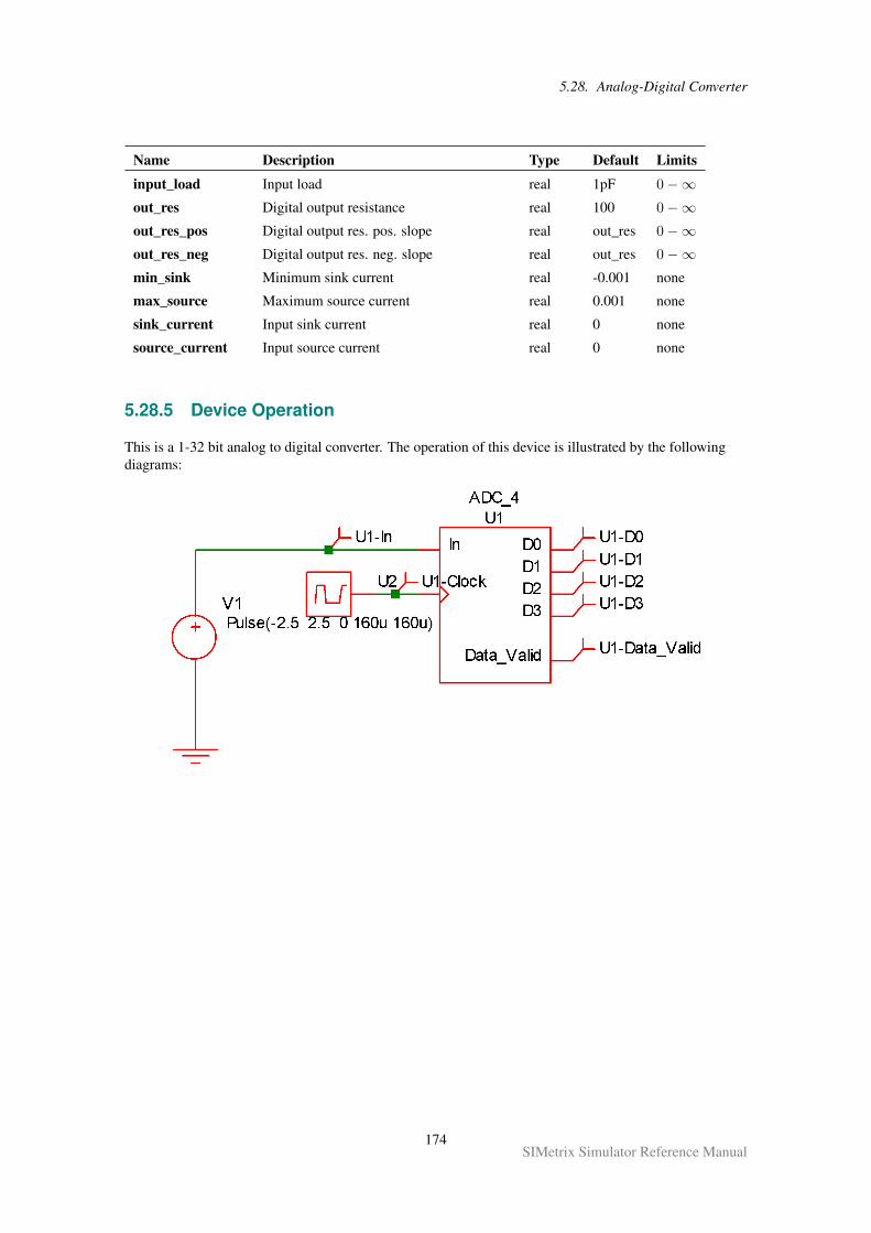
5.28. Analog-Digital Converter
Name Description Type Default Limits
input_load Input load real 1pF 0−∞out_res Digital output resistance real 100 0−∞out_res_pos Digital output res. pos. slope real out_res 0−∞out_res_neg Digital output res. neg. slope real out_res 0−∞min_sink Minimum sink current real -0.001 none
max_source Maximum source current real 0.001 none
sink_current Input sink current real 0 none
source_current Input source current real 0 none
5.28.5 Device Operation
This is a 1-32 bit analog to digital converter. The operation of this device is illustrated by the followingdiagrams:
174SIMetrix Simulator Reference Manual
5.28. Analog-Digital Converter
Conversion timings.
The ADC starts the conversion at the rising edge of the clock. The analog input signal is also sampled atthis point. The output data changes in response to this, CONVERT_TIME seconds later. At the same timethe data_valid output goes low (inactive) then high again after a delay equal to DATA_VALID_DELAY. Itis possible to start a new conversion before the previous conversion is complete provided it is started laterthan MIN_CLOCK seconds after the previous conversion was started. MIN_CLOCK must always be lessthan CONVERT_TIME. If the MIN_CLOCK specification is violated, the conversion will not start.
175SIMetrix Simulator Reference Manual
5.29. Analog-Digital Interface Bridge
5.29 Analog-Digital Interface Bridge
5.29.1 Netlist entry
Axxxx in out model_name
5.29.2 Connection details
Name Description Flow Type
in Input inout g
out Output out d
5.29.3 Model format
.MODEL model_name adc_bridge parameters
5.29.4 Model parameters
Name Description Type Default Limits
in_low Maximum 0-valued analog input real 0.1 none
in_high Minimum 1-valued analog input real 0.9 none
rise_delay Rise delay real 1nS 1e−12 −∞fall_delay Fall delay real 1nS 1e−12 −∞time_tol Threshold time tolerance real 100pS 1e−12 −∞out_low Used to calculate reflected static load. See
textreal 0 none
out_high Used to calculate reflected static load. Seetext
real 5 none
clamp_low Clamp threshold ‘ZERO’ digital input.Default to out_low
real out_low none
clamp_high Clamp threshold ‘ONE’ digital input.Default to out_high
real out_high none
clamp_res Clamp minimum resistance real 1 1e-06 −∞clamp_bias Clamp voltage real 0.8 0.2 - 2
out_family Output logic family string UNIV none
5.29.5 Device Operation
The analog-digital interface bridge is the main device used to connect analog signals to digital inputs. Thedevice produces a digital signal that is in the logic ‘1’ state when the analog input is above the highthreshold (IN_HIGH) and a logic ‘0’ state when it is below the low threshold (IN_LOW). When the analog
176SIMetrix Simulator Reference Manual
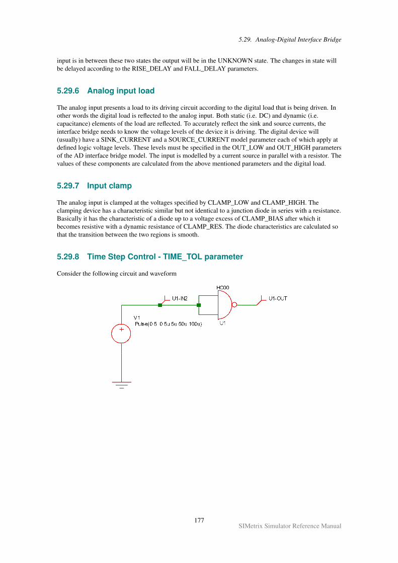
5.29. Analog-Digital Interface Bridge
input is in between these two states the output will be in the UNKNOWN state. The changes in state willbe delayed according to the RISE_DELAY and FALL_DELAY parameters.
5.29.6 Analog input load
The analog input presents a load to its driving circuit according to the digital load that is being driven. Inother words the digital load is reflected to the analog input. Both static (i.e. DC) and dynamic (i.e.capacitance) elements of the load are reflected. To accurately reflect the sink and source currents, theinterface bridge needs to know the voltage levels of the device it is driving. The digital device will(usually) have a SINK_CURRENT and a SOURCE_CURRENT model parameter each of which apply atdefined logic voltage levels. These levels must be specified in the OUT_LOW and OUT_HIGH parametersof the AD interface bridge model. The input is modelled by a current source in parallel with a resistor. Thevalues of these components are calculated from the above mentioned parameters and the digital load.
5.29.7 Input clamp
The analog input is clamped at the voltages specified by CLAMP_LOW and CLAMP_HIGH. Theclamping device has a characteristic similar but not identical to a junction diode in series with a resistance.Basically it has the characteristic of a diode up to a voltage excess of CLAMP_BIAS after which itbecomes resistive with a dynamic resistance of CLAMP_RES. The diode characteristics are calculated sothat the transition between the two regions is smooth.
5.29.8 Time Step Control - TIME_TOL parameter
Consider the following circuit and waveform
177SIMetrix Simulator Reference Manual
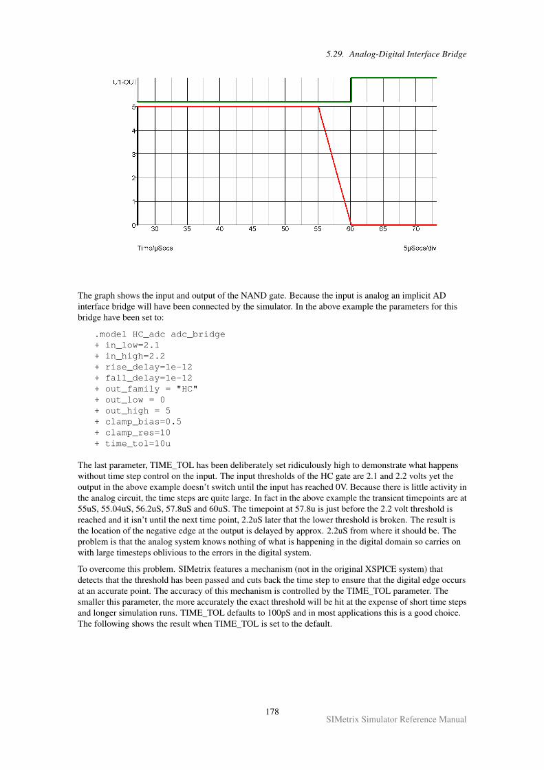
5.29. Analog-Digital Interface Bridge
The graph shows the input and output of the NAND gate. Because the input is analog an implicit ADinterface bridge will have been connected by the simulator. In the above example the parameters for thisbridge have been set to:
.model HC_adc adc_bridge+ in_low=2.1+ in_high=2.2+ rise_delay=1e-12+ fall_delay=1e-12+ out_family = "HC"+ out_low = 0+ out_high = 5+ clamp_bias=0.5+ clamp_res=10+ time_tol=10u
The last parameter, TIME_TOL has been deliberately set ridiculously high to demonstrate what happenswithout time step control on the input. The input thresholds of the HC gate are 2.1 and 2.2 volts yet theoutput in the above example doesn’t switch until the input has reached 0V. Because there is little activity inthe analog circuit, the time steps are quite large. In fact in the above example the transient timepoints are at55uS, 55.04uS, 56.2uS, 57.8uS and 60uS. The timepoint at 57.8u is just before the 2.2 volt threshold isreached and it isn’t until the next time point, 2.2uS later that the lower threshold is broken. The result isthe location of the negative edge at the output is delayed by approx. 2.2uS from where it should be. Theproblem is that the analog system knows nothing of what is happening in the digital domain so carries onwith large timesteps oblivious to the errors in the digital system.
To overcome this problem. SIMetrix features a mechanism (not in the original XSPICE system) thatdetects that the threshold has been passed and cuts back the time step to ensure that the digital edge occursat an accurate point. The accuracy of this mechanism is controlled by the TIME_TOL parameter. Thesmaller this parameter, the more accurately the exact threshold will be hit at the expense of short time stepsand longer simulation runs. TIME_TOL defaults to 100pS and in most applications this is a good choice.The following shows the result when TIME_TOL is set to the default.
178SIMetrix Simulator Reference Manual
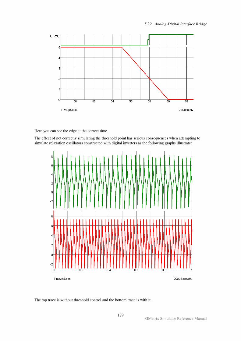
5.29. Analog-Digital Interface Bridge
Here you can see the edge at the correct time.
The effect of not correctly simulating the threshold point has serious consequences when attempting tosimulate relaxation oscillators constructed with digital inverters as the following graphs illustrate:
The top trace is without threshold control and the bottom trace is with it.
179SIMetrix Simulator Reference Manual
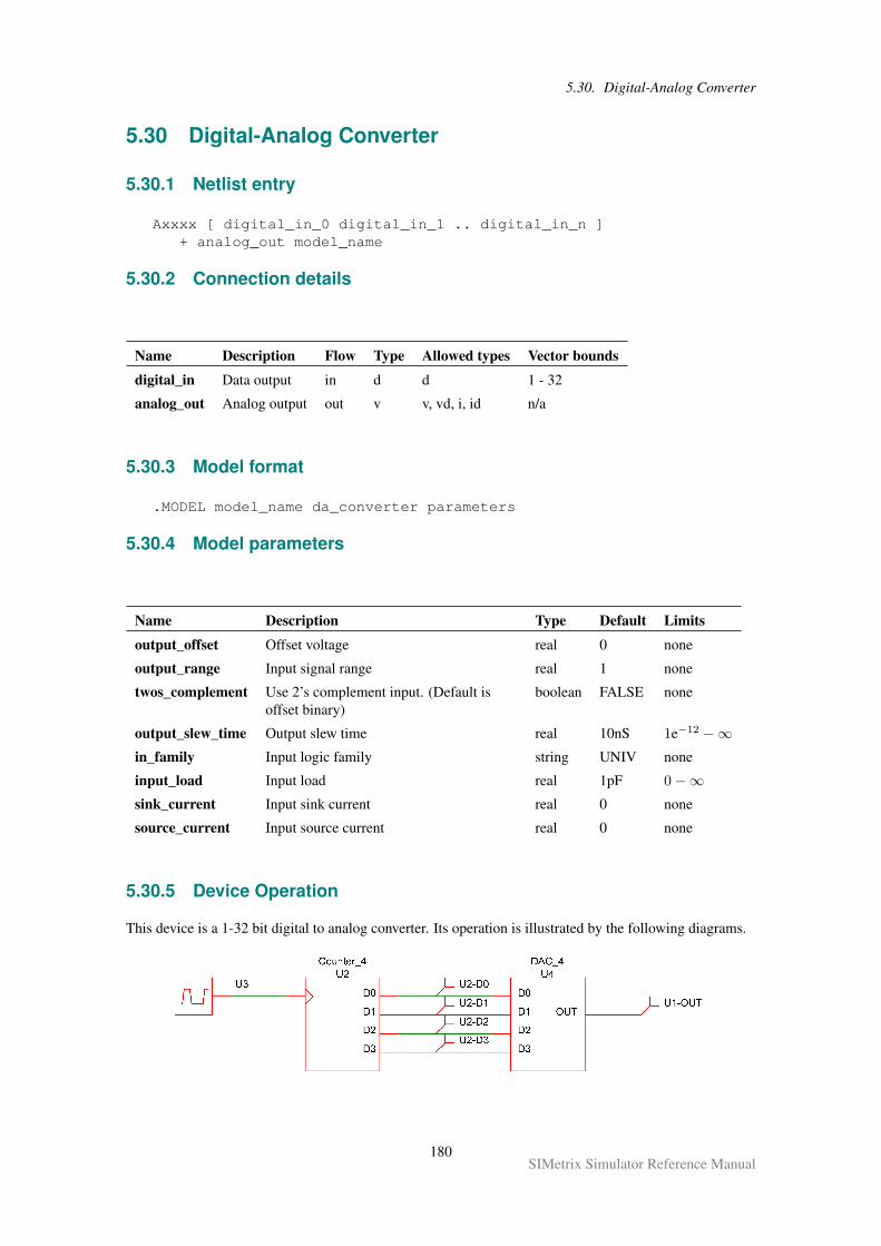
5.30. Digital-Analog Converter
5.30 Digital-Analog Converter
5.30.1 Netlist entry
Axxxx [ digital_in_0 digital_in_1 .. digital_in_n ]+ analog_out model_name
5.30.2 Connection details
Name Description Flow Type Allowed types Vector bounds
digital_in Data output in d d 1 - 32
analog_out Analog output out v v, vd, i, id n/a
5.30.3 Model format
.MODEL model_name da_converter parameters
5.30.4 Model parameters
Name Description Type Default Limits
output_offset Offset voltage real 0 none
output_range Input signal range real 1 none
twos_complement Use 2’s complement input. (Default isoffset binary)
boolean FALSE none
output_slew_time Output slew time real 10nS 1e−12 −∞in_family Input logic family string UNIV none
input_load Input load real 1pF 0−∞sink_current Input sink current real 0 none
source_current Input source current real 0 none
5.30.5 Device Operation
This device is a 1-32 bit digital to analog converter. Its operation is illustrated by the following diagrams.
180SIMetrix Simulator Reference Manual
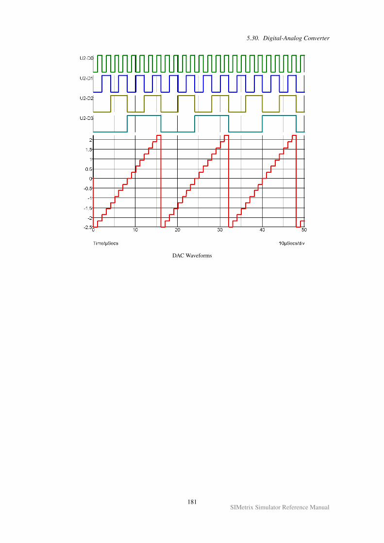
5.30. Digital-Analog Converter
DAC Waveforms
181SIMetrix Simulator Reference Manual
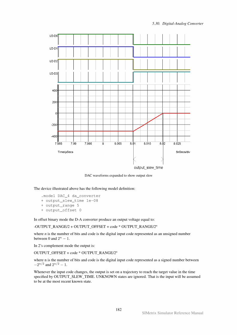
5.30. Digital-Analog Converter
DAC waveforms expanded to show output slew
The device illustrated above has the following model definition:
.model DAC_4 da_converter+ output_slew_time 1e-08+ output_range 5+ output_offset 0
In offset binary mode the D-A converter produce an output voltage equal to:
-OUTPUT_RANGE/2 + OUTPUT_OFFSET + code * OUTPUT_RANGE/2n
where n is the number of bits and code is the digital input code represented as an unsigned numberbetween 0 and 2n − 1.
In 2’s complement mode the output is:
OUTPUT_OFFSET + code * OUTPUT_RANGE/2n
where n is the number of bits and code is the digital input code represented as a signed number between−2n/2 and 2n/2 − 1.
Whenever the input code changes, the output is set on a trajectory to reach the target value in the timespecified by OUTPUT_SLEW_TIME. UNKNOWN states are ignored. That is the input will be assumedto be at the most recent known state.
182SIMetrix Simulator Reference Manual
5.31. Digital-Analog Interface Bridge
5.31 Digital-Analog Interface Bridge
5.31.1 Netlist entry
Axxxx in out model_name
5.31.2 Connection details
Name Description Flow Type
in Input in d
out Output inout g
5.31.3 Model format
.MODEL model_name dac_bridge parameters
5.31.4 Model parameters
Name Description Type Default Limits
out_low Analog output for ‘ZERO’ digitalinput
real 0 none
out_high Analog output for ‘ONE’ digitalinput
real 5 none
g_resistive Output conductance for ‘RESISTIVE’digital input
real 0.001 none
g_pullup Output conductance for ‘STRONG’digital high input
real 0.01 none
g_pulldown Output conductance for ‘STRONG’digital low input
real 0.01 none
g_hiz Output conductance for‘HI_IMPEDANCE’ strength
real 1.00E-09 none
input_load Capacitive input load (F) real 1pF none
t_rise Rise time 0 -> 1 real 1nS 1e−12 −∞t_fall Fall time 1 -> 0 real 1nS 1e−12 −∞knee_high Knee voltage logic high state real 3 none
knee_low Knee voltage logic low real 2 none
sink_current Input sink current real 0 none
source_current Input source current real 0 none
v_smooth Smoothing function offset voltage real 0 0−∞in_family Input logic family string UNIV none
183SIMetrix Simulator Reference Manual
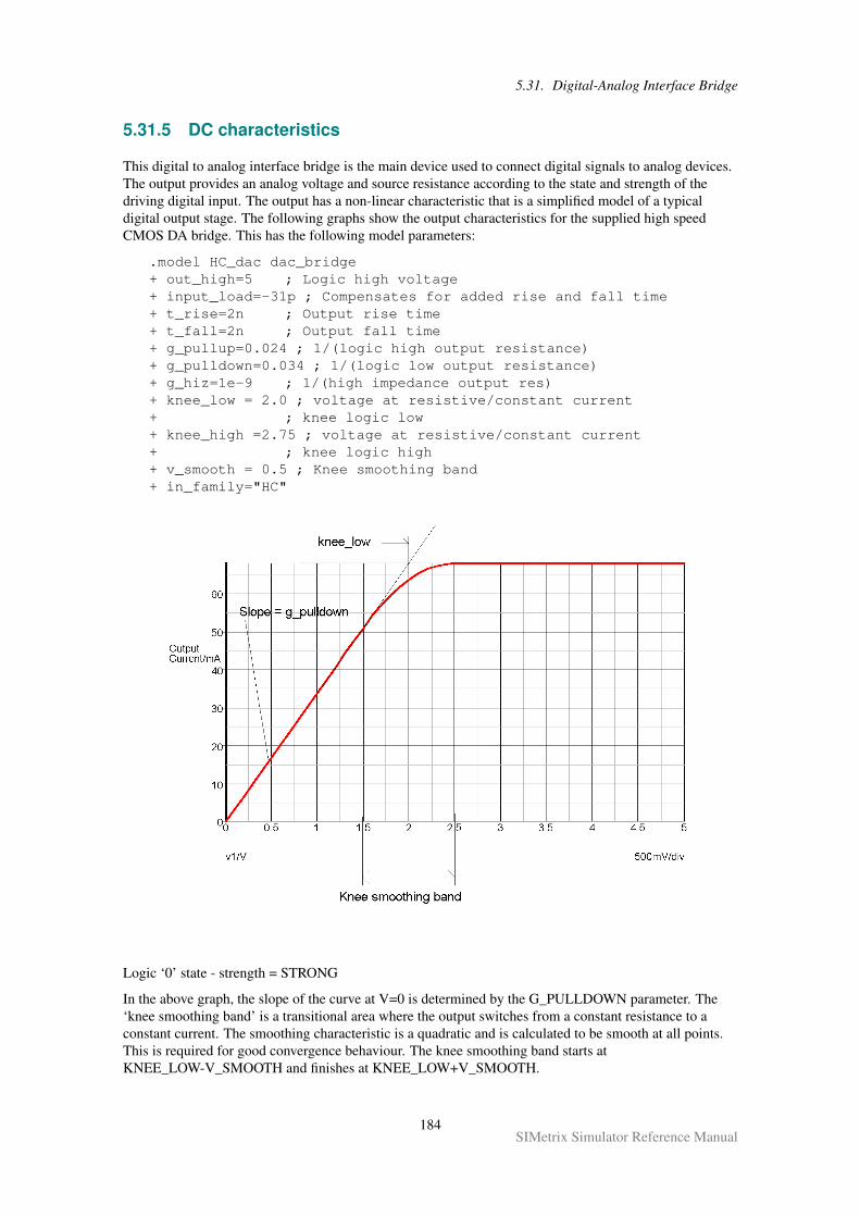
5.31. Digital-Analog Interface Bridge
5.31.5 DC characteristics
This digital to analog interface bridge is the main device used to connect digital signals to analog devices.The output provides an analog voltage and source resistance according to the state and strength of thedriving digital input. The output has a non-linear characteristic that is a simplified model of a typicaldigital output stage. The following graphs show the output characteristics for the supplied high speedCMOS DA bridge. This has the following model parameters:
.model HC_dac dac_bridge+ out_high=5 ; Logic high voltage+ input_load=-31p ; Compensates for added rise and fall time+ t_rise=2n ; Output rise time+ t_fall=2n ; Output fall time+ g_pullup=0.024 ; 1/(logic high output resistance)+ g_pulldown=0.034 ; 1/(logic low output resistance)+ g_hiz=1e-9 ; 1/(high impedance output res)+ knee_low = 2.0 ; voltage at resistive/constant current+ ; knee logic low+ knee_high =2.75 ; voltage at resistive/constant current+ ; knee logic high+ v_smooth = 0.5 ; Knee smoothing band+ in_family="HC"
Logic ‘0’ state - strength = STRONG
In the above graph, the slope of the curve at V=0 is determined by the G_PULLDOWN parameter. The‘knee smoothing band’ is a transitional area where the output switches from a constant resistance to aconstant current. The smoothing characteristic is a quadratic and is calculated to be smooth at all points.This is required for good convergence behaviour. The knee smoothing band starts atKNEE_LOW-V_SMOOTH and finishes at KNEE_LOW+V_SMOOTH.
184SIMetrix Simulator Reference Manual
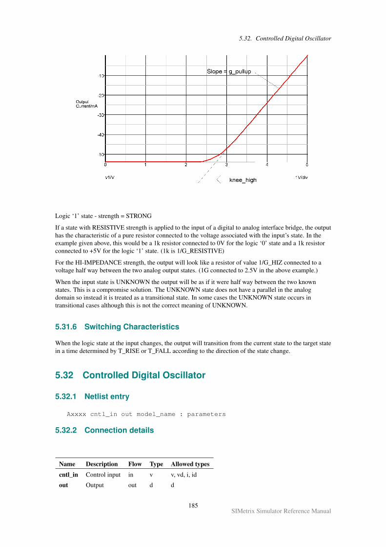
5.32. Controlled Digital Oscillator
Logic ‘1’ state - strength = STRONG
If a state with RESISTIVE strength is applied to the input of a digital to analog interface bridge, the outputhas the characteristic of a pure resistor connected to the voltage associated with the input’s state. In theexample given above, this would be a 1k resistor connected to 0V for the logic ‘0’ state and a 1k resistorconnected to +5V for the logic ‘1’ state. (1k is 1/G_RESISTIVE)
For the HI-IMPEDANCE strength, the output will look like a resistor of value 1/G_HIZ connected to avoltage half way between the two analog output states. (1G connected to 2.5V in the above example.)
When the input state is UNKNOWN the output will be as if it were half way between the two knownstates. This is a compromise solution. The UNKNOWN state does not have a parallel in the analogdomain so instead it is treated as a transitional state. In some cases the UNKNOWN state occurs intransitional cases although this is not the correct meaning of UNKNOWN.
5.31.6 Switching Characteristics
When the logic state at the input changes, the output will transition from the current state to the target statein a time determined by T_RISE or T_FALL according to the direction of the state change.
5.32 Controlled Digital Oscillator
5.32.1 Netlist entry
Axxxx cntl_in out model_name : parameters
5.32.2 Connection details
Name Description Flow Type Allowed types
cntl_in Control input in v v, vd, i, id
out Output out d d
185SIMetrix Simulator Reference Manual
5.32. Controlled Digital Oscillator
5.32.3 Instance Parameters
Name Description Type
init_phase Initial phase real
5.32.4 Model format
.MODEL model_name d_osc parameters
5.32.5 Model parameters
Name Description Type Default Limits Vectorbounds
cntl_array Control array real vector N/A none 2−∞
freq_array Frequency array real vector N/A 0−∞ 2−∞
duty_cycle Output duty cycle real 0.5 1µ -0.999999 n/a
init_phase Initial phase of output real 0 -180 - +360 n/a
rise_delay Rise delay real 1n 0−∞ n/a
fall_delay Fall delay real 1n 0−∞ n/a
phase_tol Phase tolerance/degrees real 10 0 - 45 n/a
out_family Output logic family string UNIV none n/a
out_res Digital output resistance real 100 0−∞ n/a
out_res_pos Digital output res. pos. slope real out_res 0−∞ n/a
out_res_neg Digital output res. neg. slope real out_res 0−∞ n/a
5.32.6 Device Operation
This device produces an output frequency controlled by an analog input signal following an arbitrarypiece-wise linear law. The input to output frequency characteristic is defined by two parametersCNTL_ARRAY and FREQ_ARRAY. The following is an example of a .MODEL statement:
.model vco d_osc+ cntl_array=[-1,0,1,2,3,4,5]+ freq_array=[0,10000,40000,90000,160000,250000,360000]
The frequency characteristic described by the above example follows a square law. The two arraysCNTL_ARRAY and FREQ_ARRAY must be the same length. These define the frequency output for agiven analog input.
186SIMetrix Simulator Reference Manual
5.33. Analog-Digital Schmitt Trigger
5.32.7 Time Step Control
In order to control the accuracy of the phase of the output signal, this model may cut back the analog timestep. At each analog time point, the required frequency is calculated and the digital output is set at thatfrequency. If the analog input changes by too large an amount between time points, the digital outputphase could be substantially in error as the frequency is constant between analog time points. The actualerror is calculated and if this exceeds PHASE_TOL, the time point is rejected and a time point at whichthe error will be in tolerance is estimated.
Note: This model was included with the original XSPICE code but the SIMetrix version has beencompletely re-written. The original did not have any phase error control and could not give accurate resultsunless the analog time step was artificially kept small.
5.33 Analog-Digital Schmitt Trigger
5.33.1 Netlist entry
Axxxx in out model_name
5.33.2 Connection details
Name Description Flow Type Allowed types
in Input inout g g, gd
out Output out d d
5.33.3 Model format
.MODEL model_name adc_schmitt parameters
5.33.4 Model parameters
Name Description Type Default Limits
in_low Maximum 0-valued analog input real 0.1 none
in_high Minimum 1-valued analog input real 0.9 none
rise_delay Rise delay real 1nS 1e−12 −∞fall_delay Fall delay real 1nS 1e−12 −∞time_tol Threshold time tolerance real 100pS 1e−12 −∞out_low Analog out for ‘ZERO’ input real 0 none
out_high Analog output ‘ONE’ input real 5 none
clamp_res Clamp minimum resistance real 1 1e-06 −∞clamp_bias Clamp voltage real 0.8 0.2 - 2
out_family Output logic family string UNIV none
init_cond Initial condition real 0 none
187SIMetrix Simulator Reference Manual

5.33. Analog-Digital Schmitt Trigger
5.33.5 Device Operation
This device is basically identical to the “Analog-Digital Interface Bridge” on page 176. The onlydifference is the behaviour of the device when the analog input lies between the threshold voltages. Withthe interface bridge, the output is UNKNOWN under these circumstances but with this Schmitt Trigger,the output retains its previous value and so is always in a known state. In summary, the output will onlyswitch from low to high when the input exceeds the higher threshold (IN_HIGH) and will only switchfrom high to low when the input descends below the lower threshold (IN_LOW).
If initial input voltage lies between the hysteresis thresholds, the output state is determined by theinit_cond parameter.
188SIMetrix Simulator Reference Manual
Chapter 6
Command Reference
6.1 Overview
Simulator commands instruct the simulator how to read in and simulate the circuit. All simulatorcommands begin with a period ( . ) .
For the remainder of this chapter and elsewhere in this manual, simulator commands are referred to as‘Statements’ to distinguish them from commands entered in the command shell.
The schematic editor supports some of the statements described in this chapter but not all. Unsupportedanalysis statements may be added manually to the schematic’s netlist. See “Adding Extra Netlist Lines” onpage 2 for details.
The following simulator statements are recognised by SIMetrix.
.AC
.DC
.ENDF
.ENDS
.FILE
.FUNC
.GLOBAL
.GRAPH
.IC
.INC
.INCLUDE
.KEEP
.LOAD
.LIB
.MODEL
.NOCONV
.NODESET
.NOISE
189SIMetrix Simulator Reference Manual
6.2. General Sweep Specification
.OP
.OPTION
.OPTIONS
.PARAM
.PARAMETER
.POST_PROCESS
.SENS
.SETSOA
.SUBCKT
.TEMP
.TF
.TRACE
.TRAN
The following statement is only recognised in model library files.
.ALIAS
6.2 General Sweep Specification
6.2.1 Overview
SIMetrix features a common sweeping algorithm which is used to define the swept analysis modes: .DC,.AC, .NOISE and (now) .TF, along with multiple analyses such as Monte Carlo.
The sweep algorithm has 6 modes:
• Device. Sweeps a single default value of a specified device. E.g. voltage of a voltage source,resistance of a resistor or the capacitance of a capacitor.
• Temperature
• Parameter. Parameter can be referenced in an expression for a model or instance parameter.
• Model parameter. Named model parameter.
• Frequency. (Not applicable to .DC)
• Monte Carlo. Perform a specified number of steps with distribution functions (i.e tolerances)enabled.
Standard SPICE only provides a subset of the above. .DC can only sweep voltage and current sources, .ACand .NOISE can only sweep frequency while .TF can’t be swept at all.
As well as providing 6 modes, each of the modes can sweep in four different ways. These are linear,decade, octave and list.
190SIMetrix Simulator Reference Manual
6.2. General Sweep Specification
6.2.2 Syntax
All the swept analysis modes use the same general syntax to specify the sweep parameters. However, tomaintain compatibility with SPICE and its derivatives including earlier versions of SIMetrix, each analysismode allows variations to this standard syntax. The general syntax is described below while the variationsallowed for each analysis mode are described in the section dedicated to that analysis mode.
All of the analysis modes can optionally be entered in a similar manner to .MODEL statements i.e. as anunordered list of parameter names followed by their values. For example, the following is a perfectly legalnoise analysis specification:
.noise V=vout DEVICE=V1 VN=0 F=1k LIN=(100 -10m 10m)+ INSRC=V1
In the various forms of the syntax described in the following sections, some of the parameter names maybe omitted as long as they are entered in a particular order. It is sometimes, however, easier to rememberparameter names rather than a default order, so the method described above may be more convenient forsome users.
General syntax for swept analyses
.AC|.DC|.NOISE|.TF sweep_spec [ analysis specific parameters ]
sweep_spec: One of the following:
DEVICE device_name step_spec F frequencyTEMP step_spec F frequencyPARAM param_name step_spec F frequencyMODEL model [PARAM] mod_param_name step_spec F frequencyFREQ step_specMONTE num_steps F frequency
Where
device_name Name of device to be swept. The following components may be swept:Capacitors, all controlled sources, fixed current source, fixed voltagesource, inductors and resistors.
param_name Name of parameter used in expression. Expressions may be used to definean instance or model parameter and may also be used in arbitrarysources.
model Name of model containing parameter to be swept
mod_param_name Name of model parameter
num_steps Number of steps to be performed for Monte Carlo sweep.
frequency Specified frequency for which .NOISE, .AC and .TF analyses are to beperformed. May be zero for .AC and .TF.
step_spec See below
step_spec is defined as follows:
STP start stop stepLIN num_points start stopDEC num_points_decade start stopOCT num_points_octave start stopLIST val1 [ val2 ... ]
191SIMetrix Simulator Reference Manual
6.3. Multi Step Analyses
Where:
start First value
stop Last value (inclusive)
step Interval
num_points Total number of points
num_points_decade Number of points per decade
num_points_octave Number of points per octave
STP and LIN modes are both linear sweeps but specified differently. STP specifies start, stop and a stepsize, while LIN specifies start, stop and the total number of points.
6.3 Multi Step Analyses
6.3.1 Overview
The sweep specification described in “General Sweep Specification” on page 190 can also be applied todefine multiple analyses including Monte Carlo analysis. This can be applied to the swept modes .DC,.AC, .NOISE and .TF along with .TRAN. The analyses .SENS, .PZ and .OP cannot be run in multi-stepmode. A multi-step .OP is in fact the same as .DC so this is not required. Monte Carlo analysis is thesubject of its own chapter (see “Monte Carlo Analysis” on page 256) but it is invoked in the same way asother multi-step modes. As well as the standard 6 sweep modes, small-signal multi-step analyses can berun in snapshot mode which uses snapshots created by a previous transient analysis.
6.3.2 Syntax
The general form is:
.analysis_name analysis_parameters SWEEP+ [sweep_spec] | [SNAPSHOT STP snapstart snapstop snapstep] |[SCRIPTCOUNT=numscriptruns SCRIPT=script] [ NUMCORES=num_cores]
Where:
.analysis_name Dot statement for analysis
analysis_parameters Specific parameters for that analysis
sweep_spec See “General Sweep Specification” on page 190.
SNAPSHOT Use snapshots created by a previous transient analysis. For full details, see“Snapshots” on page 253.
snapstart Index of first snapshot. Snapshots are counted in the order in which theyare created. The first is 0. Use STP 0 0 0 to specify all availablesnapshots.
snapstop Index of last snapshot
snapstep Snapshot interval (usually 1)
numscriptruns Number of repeat steps using script. If present, the script script is calledfor each step. The script may use the function GetCurrentStepValue() todetermine the step number (base 1, i.e. the first step is 1, the second 2etc.). The functions SetInstanceParamValue() and SetModelParamValue()may be used to change model or instance parameters
192SIMetrix Simulator Reference Manual
6.4. .AC
script Script called for each step
num_cores If specified and greater than 1, the work for the run will be shared amongstnum_cores processor cores using multiple processes. More informationabout using multiple cores can be found in User’s Manual/AnalysisModes/Using Multiple Cores for Multi-step Analyses.
Examples
Run 10 Monte Carlo runs for 1mS transient analysis
.TRAN 1m SWEEP MONTE 10
As above but does 1000 steps split over 4 cores. So each core will do 250 steps. Requires a systemequipped with at least 4 physical processor cores.
.TRAN 1m SWEEP MONTE 1000 NUMCORES=4
Sweep V1 from 0 to 5 volts in 0.1V steps for 200us transient
.TRAN 200u SWEEP DEVICE V1 STP 0 5 0.1
AC sweep of voltage source V5 from -300mV to 300mV. Repeat 6 times for parameter restail from 450 to550.
.AC DEVICE=V5 LIN 100 -300m 300m F=100000+ SWEEP PARAM=restail LIN 6 450 550
Run AC sweep using all available snapshots
.AC DEC 100k 10G SWEEP SNAPSHOT STP 0 0 0
6.4 .AC
6.4.1 Syntax
.AC inner_sweep_spec [ F frequency ] [RUNNAME=runname] [ SWEEP outer_sweep_spec ]
Spice compatible frequency sweep:
.AC DEC|LIN|OCT num_points start stop
Instructs the simulator to perform a swept small signal AC analysis. SIMetrix AC analysis is not limited toa frequency sweep as it is with generic SPICE and derivatives. See “General Sweep Specification” onpage 190 and examples below for more details.
frequency Frequency at which analysis will be performed for non-frequency sweeps.Default 0.
inner_sweep_spec See “General Sweep Specification” on page 190 for syntax. Defines sweepmode. FREQ keyword is optional.
outer_sweep_spec If specified, analysis will be repeated according to this specification. See“General Sweep Specification” on page 190 for syntax.
num_points LIN: total number of points DEC: number of points per decade OCT:number of points per octave
193SIMetrix Simulator Reference Manual
6.4. .AC
start Start frequency for SPICE compatible mode
stop Stop frequency for SPICE compatible mode
runname If specified, the value for runname will be passed to the simulation datagroup as a string variable with name UserRunName. This may be used toidentify which analysis generated the data which is useful when runningnetlists with multiple analyses defined
Except for frequency sweep, the frequency at which the analysis is being performed should be specified. Ifomitted, the frequency will be assumed to be zero.
For non-frequency sweeps, a new dc operating point may be calculated at each step depending on what isbeing swept. If a capacitor, inductor or an ‘AC only’ model parameter is being swept, then no new dcoperating point will be required. Otherwise one will be performed. An ‘AC only’ parameter is one thatdoes not affect DC operating point such as device capacitance.
6.4.2 Notes
An AC analysis calculates the small signal frequency response of the circuit about the dc operating point.The latter is automatically calculated prior to commencing the frequency sweep. One or more inputs maybe specified for AC analysis by using voltage or current sources with the AC specification (See “VoltageSource” on page 113). The results of an AC analysis are always complex.
6.4.3 Examples
SPICE compatible. Sweep frequency from 1kHz to 1Meg
.AC DEC 25 1k 1MEG
Sweep voltage source V1 100 points from -100mV to 100mV. Frequency = 100kHz
.AC DEVICE V1 LIN 100 -100m 100m F=100k
Sweep parameter Rscale from 0.5 to 3 in steps of 0.1. Frequency=20Meg
.AC PARAM Rscale STP 0.5 3 0.1 F=20Meg
Sweep resistor R1 with values 10k 12k 15k 18k 22k 27k 33k, Frequency =1.1KHz
.AC DEVICE R1 LIST 10k 12k 15k 18k 22k 27k 33k F=1.1K
Monte Carlo sweep 100 steps. Frequency = 10K. This is useful if - say - you are interested in the gain ofan amplifier at one frequency and it needs to lie within a defined tolerance. Previously you would need torepeat an AC sweep at a single frequency to achieve this which could take a long time especially if thecircuit has a difficult to find operating point. The analysis defined by the following line will take very littletime even for a large circuit.
.AC MONTE 100 F=10K
6.4.4 Examples of Nested Sweeps
As Monte Carlo above but repeated from 0 to 100C
.AC MONTE 100 F=10K SWEEP TEMP STP 0 100 10
... and at a number of frequencies
.AC MONTE 100 SWEEP FREQ DEC 5 1k 100k
194SIMetrix Simulator Reference Manual
6.6. .DC
6.5 .ALIAS
6.5.1 Syntax
.ALIAS alias_name device_name device_type
This statement may only be used in device model library files. It is not recognised by the simulator. Itpermits a device model or subcircuit to be referenced by a different name. This allows one modeldefinition to be used for multiple part numbers.
alias_name Alias name
device_name Device to which alias refers
device_type Type of device to which alias refers. Must be one of the following C, D,LTRA, NJF, NMF, NMOS, NPN, PJF, PMF, PMOS, PNP, R, SW orSUBCKT. see “.MODEL” on page 214 for more details.
6.5.2 Example
.MODEL BC547C NPN+ IS=7.59E-15 VAF=19.3 BF=500 IKF=0.0710 NE=1.3808+ ISE=7.477E-15 IKR=0.03 ISC=2.00E-13 NC=1.2 NR=1 BR=5+ RC=0.75 CJC=6.33E-12 FC=0.5 MJC=0.33 VJC=0.65+ CJE=1.25E-11 MJE=0.55 VJE=0.65 TF=4.12E-10 ITF=0.4 VTF=3+ XTF=12.5 RB=172 IRB=0.000034 RBM=65
.ALIAS BC549C BC547C NPN
The above would provide identical definitions for both BC547C and BC549C bipolar transistors.
Notes .ALIAS definitions will recognise models defined in other files provided the file inwhich the alias resides and the file in which the model definition resides are part ofthe same library specification. A library specification is a single pathname possiblywith a wildcard (‘?’ or ‘*’) to refer to multiple files. E.g. /simetrix/models/*.mod is alibrary specification and refers to all files with the extension ‘.mod’ in the directory/simetrix/models.
Aliases must refer directly to a model or subcircuit definition and not to otheraliases.
6.6 .DC
6.6.1 Syntax
.DC inner_sweep_spec [RUNNAME=runname] [ SWEEP outer_sweep_spec ]
Spice compatible:
.DC device_name start stop step
The remainder are SIMetrix 2.5 - 3.1 compatible:
.DC TEMP start stop step
195SIMetrix Simulator Reference Manual
6.6. .DC
.DC PARAM param_name start stop step
.DC MODEL model [PARAM] mod_param_name start stop step
Instructs simulator to perform a DC sweep analysis. A dc analysis performs a dc operating point analysisfor a range of values according to the sweep specification. SIMetrix DC analysis is not limited to sweepinga voltage or current source as with generic SPICE. Any mode defined by the general sweep specification(see “General Sweep Specification” on page 190) may be used although frequency sweep has no usefulpurpose.
inner_sweep_spec See “General Sweep Specification” on page 190 for syntax. Defines sweepmode. DEVICE keyword is optional.
outer_sweep_spec If specified, analysis will be repeated according to this specification. See“Multi Step Analyses” on page 192 for details.
device_name Component reference of voltage source, current source, resistor orcontrolled source to be swept. (Only voltage and current sources areSPICE compatible).
start Start value for sweep
stop Stop value for sweep
step Increment at each point
param_name Parameter name. This would be used in an expression to define acomponent or model value.
model_name Model name e.g. Q2N2222
model_parameter_name Model parameter name e.g. IS
runname If specified, the value for runname will be passed to the simulation datagroup as a string variable with name UserRunName. This may be used toidentify which analysis generated the data which is useful when runningnetlists with multiple analyses defined.
If start is arithmetically greater than stop then step must be negative.
It is not necessary to declare parameters with .PARAM if using parameter sweep.
6.6.2 Examples
SPICE compatible. Sweep V1 from 0 to 5 volts in steps of 0.1 volt
.DC V1 0 5 0.1
SIMetrix 3.1 compatible temperature sweep
.DC TEMP 0 100 2
Decade (i.e. logarithmic) sweep. Sweep V1 from 1mV to 1V with 25 points per decade
.DC V1 DEC 25 1m 1v
Note that the DEVICE keyword has been omitted. This is the default sweep mode for .DC.
Do 1000 Monte Carlo steps. This performs the same task as a Monte Carlo analysis applied to a DCoperating point. In other products and earlier versions of SIMetrix this task would take a long time as theoperating point is solved from scratch each time. With the mode described by the following example, theoperating point need only be calculated from scratch once. All subsequent steps are seeded by the previousone and usually require only a few iterations. The end result is a sometimes spectacular increase in speed.
.DC MONTE 1000
196SIMetrix Simulator Reference Manual
6.7. .FILE and .ENDF
6.6.3 Examples of Nested Sweeps
Decade sweep at temperatures 0 to 100 in steps of 10
.DC V1 DEC 25 1m 1v SWEEP TEMP STP 0 100 10
Note the STP keyword is necessary to signify the start-stop-step method of defining a linear sweep.Alternatively LIN can be used which defines the sweep in terms of the total number of points. Thefollowing is equivalent to the above:
.DC V1 DEC 25 1m 1v SWEEP TEMP LIN 11 0 100
Do 100 run Monte Carlo analysis for temperature sweep
.DC TEMP 0 100 2 SWEEP MONTE 100
6.7 .FILE and .ENDF
6.7.1 Syntax
.FILE filenamefile_contents.ENDF
The .FILE statement allows the contents of a file referenced in a .MODEL statement to be placed directlyin the netlist. Files are referenced in arbitrary logic blocks (see “Arbitrary Logic Block - User DefinedModels” on page 294), PWLFILE voltage and current sources (see “PWL File Source” on page 115),digital sources (see “Digital Signal Source” on page 145) and digital state machines (see “State Machine”on page 165). Each of these may refer to files defined using .FILE and .ENDF.
6.7.2 Example
.MODEL COUNT_8 d_logic_block file=counter_def
.FILE counter_defPORT (DELAY = 10n) CountOut out[0:7] ;
EDGE (DELAY=5n, WIDTH=8, CLOCK=in[0]) Count ;
ount = Count + 1 ;
CountOut = count ;.ENDF
The .MODEL statement refers to a file called ‘counter_def’. This could be a real disk file calledcounter_def or counter_def.ldf, but in the above example it is instead defined directly in the netlist using.FILE and .ENDF.
6.7.3 Important Note
.FILE and .ENDF will not be recognised in library files.
197SIMetrix Simulator Reference Manual

6.8. .FUNC
6.8 .FUNC
.FUNC name ( [arglist] ) body
198SIMetrix Simulator Reference Manual
6.9. .GLOBAL
name Name of function. Must begin with a letter and not match one of the builtin functions.
arglist List of comma separated argument names. May be empty in which casethe function may be called without the parentheses. This is useful forcreating random variables for Monte Carlo analysis.
body Body of function. This is an expression referring to the names in arglistthat defines the operation performed by the function
.FUNC defines a function that can be used in a model or device parameter expression, a parameter definedusing .PARAM or in an arbitrary source expression.
6.8.1 Examples
.FUNC FREQ(V) (V)*120K
.FUNC SWEEP(V) SIN(TIME*FREQ(v)*2*PI)
.FUNC RV1() GAUSS(0.1)
The third example may be called without parentheses as it has no arguments. E.g.:
.PARAM random1 = rv1 random2 = rv1
In the above, random1 and random2 will have different values when run in a Monte Carlo analysis.
6.8.2 Optimiser
Any expression that uses a function defined with .FUNC will be automatically processed by anoptimisation algorithm. For more information see “Optimisation” on page 28.
The optimiser attempts to speed simulations by making the expression evaluation more efficient. Theoptimiser is effective when .FUNC is used to create very complex expressions perhaps to develop asemiconductor device. In simple applications it may not make a noticeable improvement to performance.The optimiser can be enabled for all expressions and can also be disabled completely. To enable for allexpressions use:
.OPTIONS optimise=2
To disable:
.OPTIONS optimise=0
6.9 .GLOBAL
.GLOBAL node [ node... ]
Identifies nodes as global. This allows nodes specified at the top level of a circuit to be accessed within asubcircuit definition. For more information see “Subcircuits” on page 29.
6.10 .GRAPH
6.10.1 Parameters
199SIMetrix Simulator Reference Manual
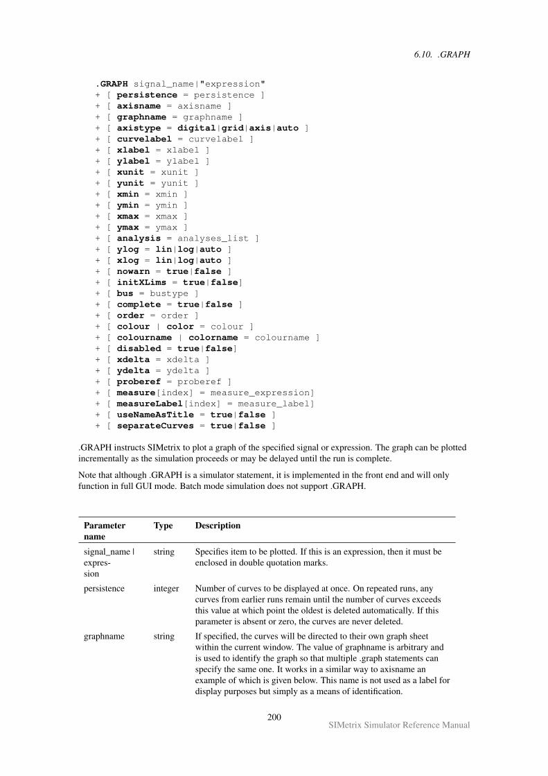
6.10. .GRAPH
.GRAPH signal_name|"expression"+ [ persistence = persistence ]+ [ axisname = axisname ]+ [ graphname = graphname ]+ [ axistype = digital|grid|axis|auto ]+ [ curvelabel = curvelabel ]+ [ xlabel = xlabel ]+ [ ylabel = ylabel ]+ [ xunit = xunit ]+ [ yunit = yunit ]+ [ xmin = xmin ]+ [ ymin = ymin ]+ [ xmax = xmax ]+ [ ymax = ymax ]+ [ analysis = analyses_list ]+ [ ylog = lin|log|auto ]+ [ xlog = lin|log|auto ]+ [ nowarn = true|false ]+ [ initXLims = true|false]+ [ bus = bustype ]+ [ complete = true|false ]+ [ order = order ]+ [ colour | color = colour ]+ [ colourname | colorname = colourname ]+ [ disabled = true|false]+ [ xdelta = xdelta ]+ [ ydelta = ydelta ]+ [ proberef = proberef ]+ [ measure[index] = measure_expression]+ [ measureLabel[index] = measure_label]+ [ useNameAsTitle = true|false ]+ [ separateCurves = true|false ]
.GRAPH instructs SIMetrix to plot a graph of the specified signal or expression. The graph can be plottedincrementally as the simulation proceeds or may be delayed until the run is complete.
Note that although .GRAPH is a simulator statement, it is implemented in the front end and will onlyfunction in full GUI mode. Batch mode simulation does not support .GRAPH.
Parametername
Type Description
signal_name |expres-sion
string Specifies item to be plotted. If this is an expression, then it must beenclosed in double quotation marks.
persistence integer Number of curves to be displayed at once. On repeated runs, anycurves from earlier runs remain until the number of curves exceedsthis value at which point the oldest is deleted automatically. If thisparameter is absent or zero, the curves are never deleted.
graphname string If specified, the curves will be directed to their own graph sheetwithin the current window. The value of graphname is arbitrary andis used to identify the graph so that multiple .graph statements canspecify the same one. It works in a similar way to axisname anexample of which is given below. This name is not used as a label fordisplay purposes but simply as a means of identification.
200SIMetrix Simulator Reference Manual
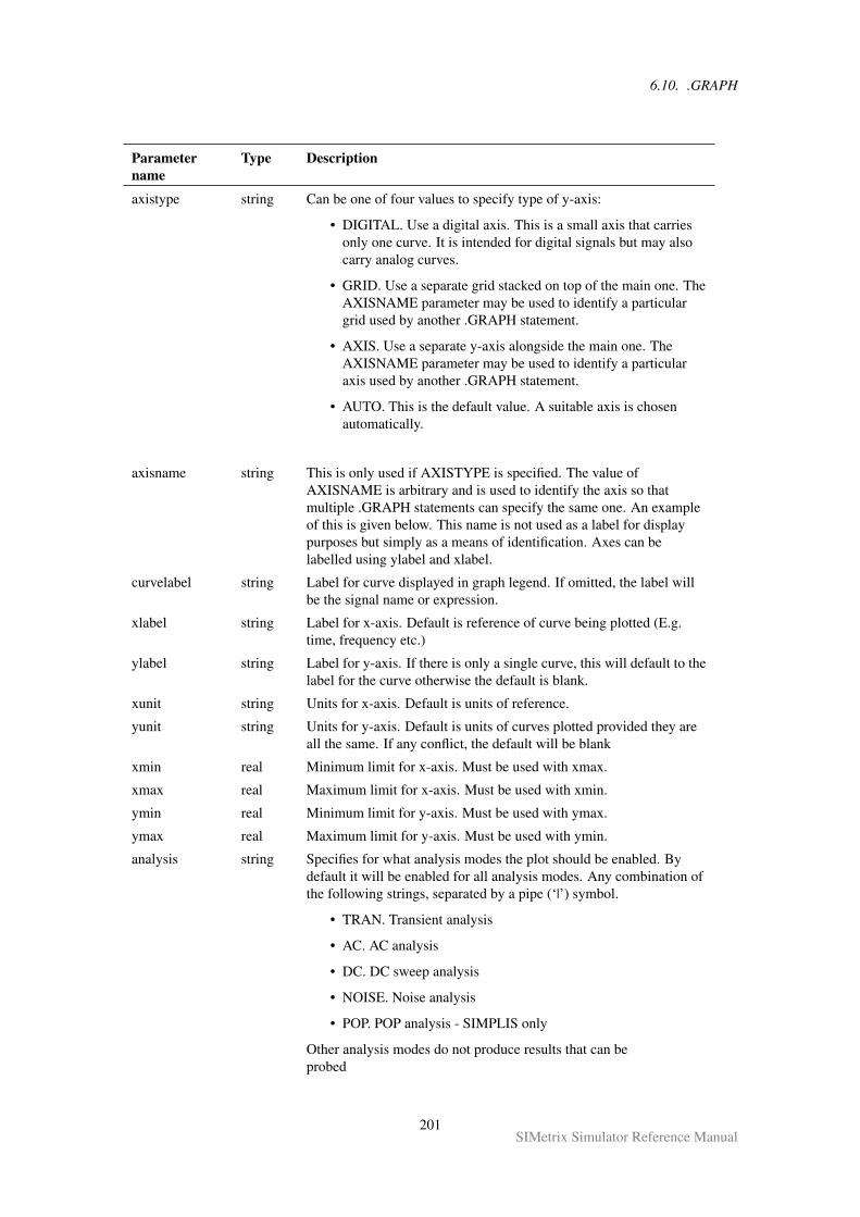
6.10. .GRAPH
Parametername
Type Description
axistype string Can be one of four values to specify type of y-axis:
• DIGITAL. Use a digital axis. This is a small axis that carriesonly one curve. It is intended for digital signals but may alsocarry analog curves.
• GRID. Use a separate grid stacked on top of the main one. TheAXISNAME parameter may be used to identify a particulargrid used by another .GRAPH statement.
• AXIS. Use a separate y-axis alongside the main one. TheAXISNAME parameter may be used to identify a particularaxis used by another .GRAPH statement.
• AUTO. This is the default value. A suitable axis is chosenautomatically.
axisname string This is only used if AXISTYPE is specified. The value ofAXISNAME is arbitrary and is used to identify the axis so thatmultiple .GRAPH statements can specify the same one. An exampleof this is given below. This name is not used as a label for displaypurposes but simply as a means of identification. Axes can belabelled using ylabel and xlabel.
curvelabel string Label for curve displayed in graph legend. If omitted, the label willbe the signal name or expression.
xlabel string Label for x-axis. Default is reference of curve being plotted (E.g.time, frequency etc.)
ylabel string Label for y-axis. If there is only a single curve, this will default to thelabel for the curve otherwise the default is blank.
xunit string Units for x-axis. Default is units of reference.
yunit string Units for y-axis. Default is units of curves plotted provided they areall the same. If any conflict, the default will be blank
xmin real Minimum limit for x-axis. Must be used with xmax.
xmax real Maximum limit for x-axis. Must be used with xmin.
ymin real Minimum limit for y-axis. Must be used with ymax.
ymax real Maximum limit for y-axis. Must be used with ymin.
analysis string Specifies for what analysis modes the plot should be enabled. Bydefault it will be enabled for all analysis modes. Any combination ofthe following strings, separated by a pipe (‘|’) symbol.
• TRAN. Transient analysis
• AC. AC analysis
• DC. DC sweep analysis
• NOISE. Noise analysis
• POP. POP analysis - SIMPLIS only
Other analysis modes do not produce results that can beprobed
201SIMetrix Simulator Reference Manual
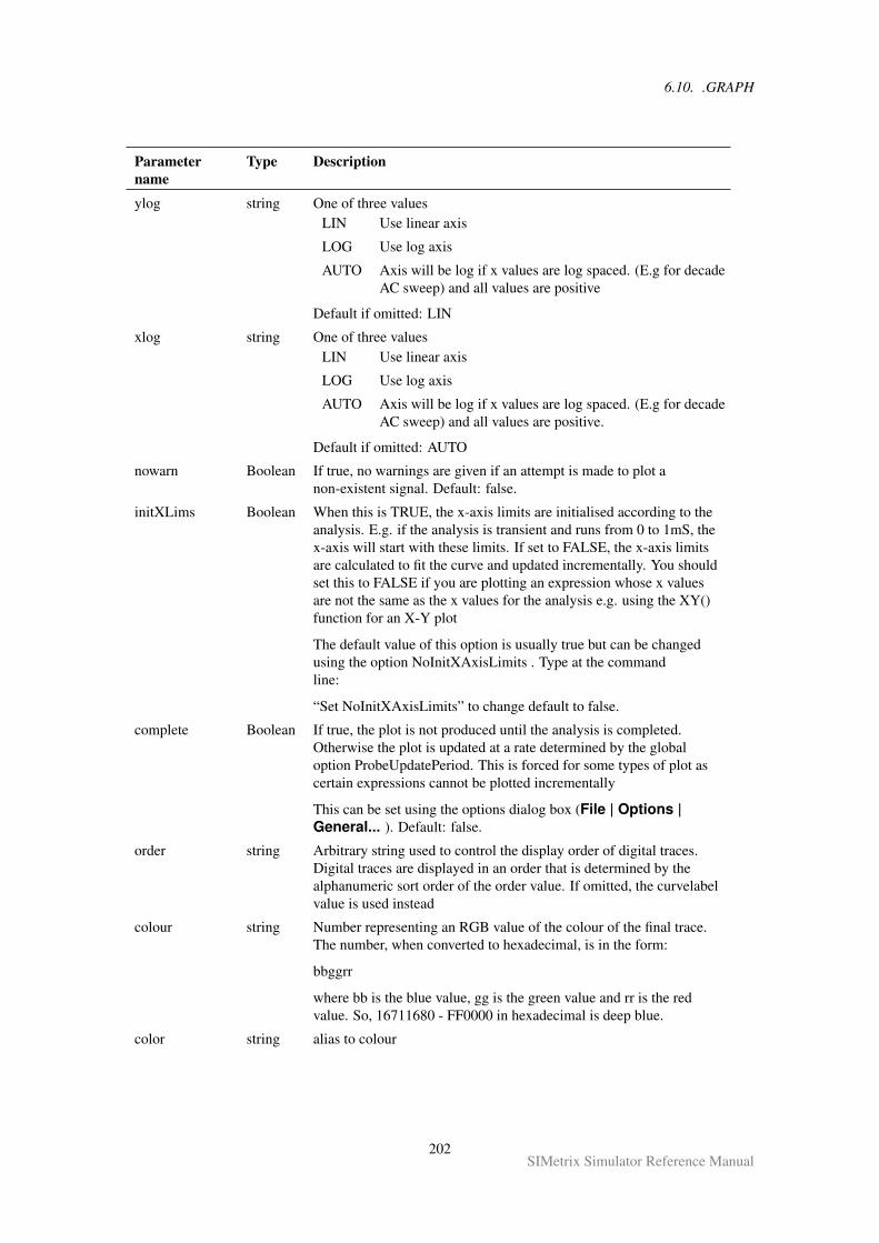
6.10. .GRAPH
Parametername
Type Description
ylog string One of three valuesLIN Use linear axis
LOG Use log axis
AUTO Axis will be log if x values are log spaced. (E.g for decadeAC sweep) and all values are positive
Default if omitted: LIN
xlog string One of three valuesLIN Use linear axis
LOG Use log axis
AUTO Axis will be log if x values are log spaced. (E.g for decadeAC sweep) and all values are positive.
Default if omitted: AUTO
nowarn Boolean If true, no warnings are given if an attempt is made to plot anon-existent signal. Default: false.
initXLims Boolean When this is TRUE, the x-axis limits are initialised according to theanalysis. E.g. if the analysis is transient and runs from 0 to 1mS, thex-axis will start with these limits. If set to FALSE, the x-axis limitsare calculated to fit the curve and updated incrementally. You shouldset this to FALSE if you are plotting an expression whose x valuesare not the same as the x values for the analysis e.g. using the XY()function for an X-Y plot
The default value of this option is usually true but can be changedusing the option NoInitXAxisLimits . Type at the commandline:
“Set NoInitXAxisLimits” to change default to false.
complete Boolean If true, the plot is not produced until the analysis is completed.Otherwise the plot is updated at a rate determined by the globaloption ProbeUpdatePeriod. This is forced for some types of plot ascertain expressions cannot be plotted incrementally
This can be set using the options dialog box (File | Options |General... ). Default: false.
order string Arbitrary string used to control the display order of digital traces.Digital traces are displayed in an order that is determined by thealphanumeric sort order of the order value. If omitted, the curvelabelvalue is used instead
colour string Number representing an RGB value of the colour of the final trace.The number, when converted to hexadecimal, is in the form:
bbggrr
where bb is the blue value, gg is the green value and rr is the redvalue. So, 16711680 - FF0000 in hexadecimal is deep blue.
color string alias to colour
202SIMetrix Simulator Reference Manual
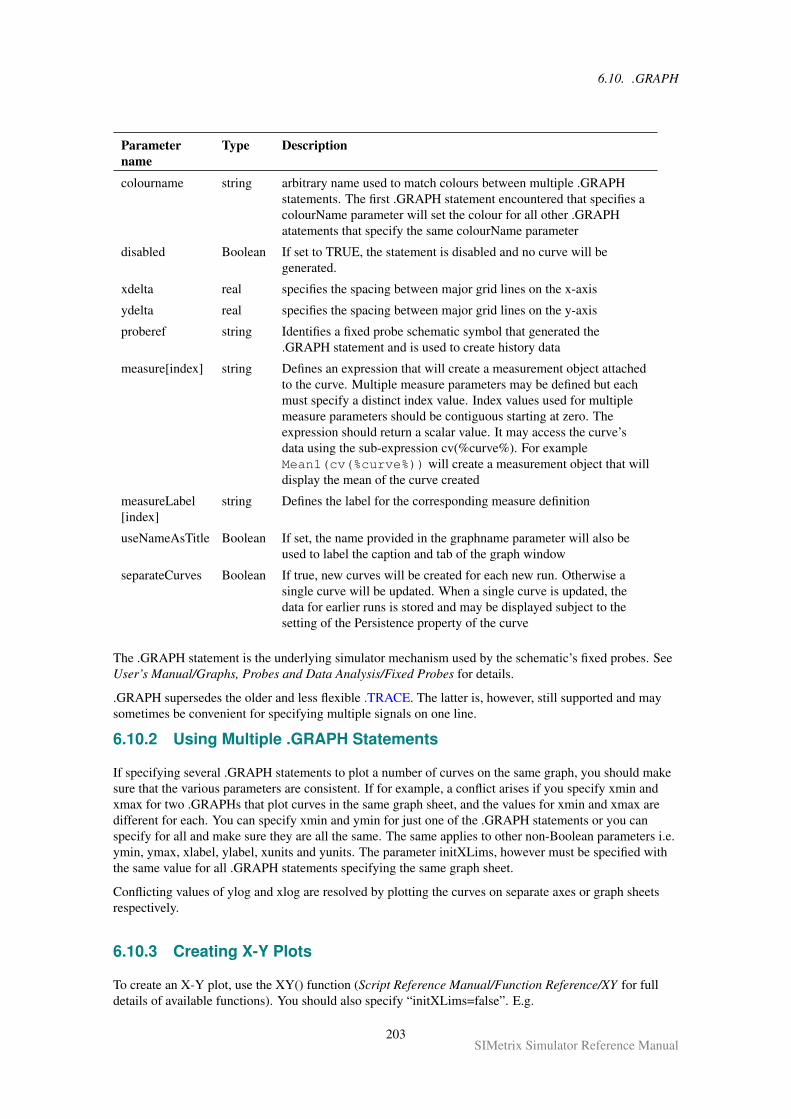
6.10. .GRAPH
Parametername
Type Description
colourname string arbitrary name used to match colours between multiple .GRAPHstatements. The first .GRAPH statement encountered that specifies acolourName parameter will set the colour for all other .GRAPHatatements that specify the same colourName parameter
disabled Boolean If set to TRUE, the statement is disabled and no curve will begenerated.
xdelta real specifies the spacing between major grid lines on the x-axis
ydelta real specifies the spacing between major grid lines on the y-axis
proberef string Identifies a fixed probe schematic symbol that generated the.GRAPH statement and is used to create history data
measure[index] string Defines an expression that will create a measurement object attachedto the curve. Multiple measure parameters may be defined but eachmust specify a distinct index value. Index values used for multiplemeasure parameters should be contiguous starting at zero. Theexpression should return a scalar value. It may access the curve’sdata using the sub-expression cv(%curve%). For exampleMean1(cv(%curve%)) will create a measurement object that willdisplay the mean of the curve created
measureLabel[index]
string Defines the label for the corresponding measure definition
useNameAsTitle Boolean If set, the name provided in the graphname parameter will also beused to label the caption and tab of the graph window
separateCurves Boolean If true, new curves will be created for each new run. Otherwise asingle curve will be updated. When a single curve is updated, thedata for earlier runs is stored and may be displayed subject to thesetting of the Persistence property of the curve
The .GRAPH statement is the underlying simulator mechanism used by the schematic’s fixed probes. SeeUser’s Manual/Graphs, Probes and Data Analysis/Fixed Probes for details.
.GRAPH supersedes the older and less flexible .TRACE. The latter is, however, still supported and maysometimes be convenient for specifying multiple signals on one line.
6.10.2 Using Multiple .GRAPH Statements
If specifying several .GRAPH statements to plot a number of curves on the same graph, you should makesure that the various parameters are consistent. If for example, a conflict arises if you specify xmin andxmax for two .GRAPHs that plot curves in the same graph sheet, and the values for xmin and xmax aredifferent for each. You can specify xmin and ymin for just one of the .GRAPH statements or you canspecify for all and make sure they are all the same. The same applies to other non-Boolean parameters i.e.ymin, ymax, xlabel, ylabel, xunits and yunits. The parameter initXLims, however must be specified withthe same value for all .GRAPH statements specifying the same graph sheet.
Conflicting values of ylog and xlog are resolved by plotting the curves on separate axes or graph sheetsrespectively.
6.10.3 Creating X-Y Plots
To create an X-Y plot, use the XY() function (Script Reference Manual/Function Reference/XY for fulldetails of available functions). You should also specify “initXLims=false”. E.g.
203SIMetrix Simulator Reference Manual
6.10. .GRAPH
.GRAPH "XY( imag(vout), real(vout) )" initXLims=false+ xlog=LIN complete=true
The above will create a Nyquist plot of the vector VOUT.
6.10.4 Using .GRAPH in Subcircuits
.GRAPH maybe used in a subcircuit in which case a plot will be produced for all instances of thatsubcircuit. Note, however, that it will only work for single values and not for expressions when inside asubcircuit. The value of the curveLabel parameter will be prefixed with the instance name so that thedisplayed curves can be correctly identified.
6.10.5 Using Expressions with .GRAPH
You can enter an expression as well as single vectors to be plotted. A problem arises when plottingexpressions incrementally that are regularly updated while the simulation is running. SIMetrix versionsprior to v5 could not incrementally evaluate expressions, so each time the plot of an expression wasupdated, the expression had to be recalculated from the beginning. This was inefficient and it has alwaysbeen recommended that the complete=true flag was added in these circumstance to inhibit incrementalplotting.
SIMetrix - from version 5 - now has the ability to incrementally evaluate some expressions and there is nolonger a recommendation to set complete=true. However, certain expression cannot be incrementallyevaluated and when such expressions are entered, incremental plotting will automatically be disabled andthe plot won’t appear until the run is complete.
A notable example of expressions that cannot be incrementally evaluated is anything containing thephase() function. This is because the phase() function uses a state machine to determine when the phasewraps from -180 to 180 and back. An offset is then applied to make the phase plot continuous. Because ofthe state machine, it is always necessary to evaluate this function from start to finish which makesincremental evaluation difficult. An alternative is to use instead the arg() function. This is the same asphase, but does not have the state machine and always gives an output that lies between +/- 180 degrees.
6.10.6 Plotting Spectra with .GRAPH
You can use .GRAPH to create spectrum plots using FFTs or Fourier. However, FFT is quite difficult touse on its own as it needs interpolated data. So, a new user defined function called Spectrum() has beendeveloped that is especially designed for use with .GRAPH. Usage is:
Spectrum(vector, numPoints [, start [, stop]])
Where:
vector Vector or expression
numPoints FFT size - must be a binary power of 2
start Start time - default = 0
stop Stop time - default = end of data
Spectrum() cannot be incrementally evaluated and so incremental plotting will automatically be disabledfor any .GRAPH statement that uses it. See “Using Expressions with .GRAPH” on page 204.
Examples
204SIMetrix Simulator Reference Manual
6.11. .IC
.GRAPH C2_P curveLabel="Amplifier output" nowarn=true
Plots the vector C2_P and gives it the label ‘Amplifier output’. As NOWARN is TRUE, no warning will begiven if C2_P does not exist.
.GRAPH vout_quad+ axisType="grid"+ axisName="grid1"+ persistence=2+ curveLabel="Quadrature"+ nowarn=true+ analysis = TRAN|DC
.GRAPH vout+ axisType="grid"+ axisName="grid1"+ persistence=2+ curveLabel="In Phase"+ yLabel="Filter Outputs"+ nowarn=true+ analysis = TRAN|DC
The above illustrates the use of the parameters AXISTYPE and AXISNAME. Both the vectors specifiedby the above .GRAPH statements will be plotted on the same but separate grid. Because both grids havebeen given the AXISNAME grid1, each curve will be plotted on the same one. If the values of axisnamefor the above were different, each curve would be plotted on a separate grid. The ANALYSIS parameterhas been specified in both cases, so plots will only be created for transient and dc sweep analyses.
6.11 .IC
.IC V(node1)=val1 [ V(node2)=val2 ]...
OR
.IC node1 val1 [ node2 val2 ]
This statement sets transient analysis initial conditions.
node1, node2 etc. Name of circuit node (or net) to which initial condition is to be applied.See notes below.
val1, val2 etc. Voltage to be applied to net as initial condition. May be an expressioncontaining parameters defined using .PARAM.
If the UIC parameter is specified with the .TRAN statement no DC operating point will be calculated so aninitial condition will set the bias point in the same way as an IC=... parameter on a BJT, capacitor, diode,JFET or MOSFET.
If the UIC parameter is absent from the .TRAN statement then a DC operating point is calculated beforethe transient analysis. In this case the net voltages specified on the .IC statement are forced to the desiredinitial values during the DC operating point solution. Once transient analysis begins this constraint isreleased. By default the voltage force is effectively carried out via a 1Ω resistor. This can be changed withthe option setting ICRES (see “.OPTIONS” on page 221).
6.11.1 Alternative Initial Condition Implementations
An initial condition can also be specified using a voltage source with the DCOP parameter specified. E.g.
205SIMetrix Simulator Reference Manual
6.13. .KEEP
VIC1 2 3 3.5 DCOP
Will force a voltage of 3.5 volts between nodes 2 and 3 during the DC operating point solution. This hastwo advantages over .IC:
1. It has zero force resistance
2. It can be applied differentially
You can also use a capacitor with the BRANCH parameter set to 1. E.g.:
C1 2 3 10u BRANCH=1 IC=3.5
This will behave identically to the voltage source in the above example during the DC operating point butduring a subsequent small-signal or transient analysis will present a 10 F capacitance to nodes 2 and 3.
See also: “Capacitor” on page 55 and “Voltage Source” on page 113.
6.12 .INC
.INC pathname
Insert the contents of the specified file.
pathname File system pathname for file to be included
The .INC statement is replaced by the specified file in its entirety as if was part of the original file. .INCstatements may also be nested i.e. there may be .INC statements within the included file. Nesting may beto any level.
6.13 .KEEP
.KEEP signal_spec [signal_spec ...]
This statement tells the simulator what values to store during a simulation. By default all signals at the toplevel and defined inside a hierarchical subcircuit are saved. .KEEP may be used in conjunction with some.OPTIONS settings to increase or reduce the data saved.
signal_spec /TOP | /SUBS | /NOV | /NOI | /NODIG | /INTERNAL | *V | *I | *D |**V | **I | **D | subref.*V | subref.*I | subref.*D | subref.**V | subref.**I| subref.**D | ˆwildcard_filter | signal_name
subref Sub-circuit reference
/NOV Don’t store top level (i.e. not in a subcircuit) voltages. Equivalent to“.OPTIONS KeepNov”
/NOI Don’t store top level currents. Equivalent to “.OPTIONS KeepNoi”
/NODIG Don’t store top level digital data. Equivalent to “.OPTIONSKeepNod”
/SUBS Store all subcircuit data. Equivalent to “.OPTIONS KeepAll”
/TOP Overrides /subs. This is to inhibit storing signals in child schematics inhierarchical designs. Equivalent to “.OPTIONS KeepTop”
206SIMetrix Simulator Reference Manual
6.13. .KEEP
/INTERNAL Save all internal device values. Some devices have internal nodes orsources. For example the bipolar transistor has internal nodes toimplement terminal resistance. These internal values are not usually savedbut may be by specifying /INTERNAL. Equivalent to “.OPTIONSKeepInternal”
ˆwildcard_filter General specification that selects values to store based on their namealone. Would usually use one of the special characters ‘*’ and ‘?’. ‘*’means ‘match one or more characters’ while ‘?’ means ‘match a singlecharacter’. Some examples:
* matches anything
X1.* matches any signal name that starts with the three letters:X1.
X?.* matches any name that starts with an X and with a ‘.’ forthe third letter.
*.q10#c matches any name ending with q10#c.
*V Store all top level voltages. This is actually implicit and need not bespecified at the top level of the netlist. It can be usefully used insub-circuit definitions - see notes.
*I Store all top level currents. This is actually implicit and need not bespecified at the top level of the netlist. It can be usefully used insub-circuit definitions - see notes.
*D Store all top level digital data. This is actually implicit and need not bespecified at the top level of the netlist. It can be usefully used insub-circuit definitions - see notes.
**V Store all voltages including those inside sub-circuits descending to alllevels
**I Store all currents including those inside sub-circuits descending to alllevels
**D Store all digital data including those inside sub-circuits descending to alllevels
subref.*V Store all voltages within sub-circuit subref excluding voltages withinchildren of subref.
subref.*I Store all currents within sub-circuit subref excluding currents withinchildren of subref.
subref.*D Store all digital data within sub-circuit subref excluding digital datawithin children of subref.
subref.**V Store all voltages within sub-circuit subref including voltages withinchildren of subref descending to all levels.
subref.*I Store all currents within sub-circuit subref including currents withinchildren of subref descending to all levels.
subref.*D Store all digital data within sub-circuit subref including digital data withinchildren of subref descending to all levels.
signal_name Explicit voltage or current.
6.13.1 Option Settings
A number of option settings are available to control data output. These can be used in conjunction with.KEEP statements to define what data is saved. The Option settings are defined in the table below:
207SIMetrix Simulator Reference Manual
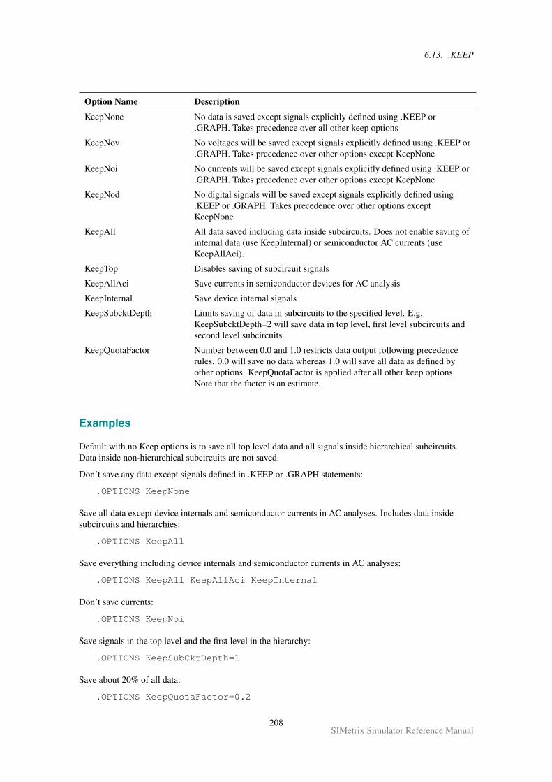
6.13. .KEEP
Option Name Description
KeepNone No data is saved except signals explicitly defined using .KEEP or.GRAPH. Takes precedence over all other keep options
KeepNov No voltages will be saved except signals explicitly defined using .KEEP or.GRAPH. Takes precedence over other options except KeepNone
KeepNoi No currents will be saved except signals explicitly defined using .KEEP or.GRAPH. Takes precedence over other options except KeepNone
KeepNod No digital signals will be saved except signals explicitly defined using.KEEP or .GRAPH. Takes precedence over other options exceptKeepNone
KeepAll All data saved including data inside subcircuits. Does not enable saving ofinternal data (use KeepInternal) or semiconductor AC currents (useKeepAllAci).
KeepTop Disables saving of subcircuit signals
KeepAllAci Save currents in semiconductor devices for AC analysis
KeepInternal Save device internal signals
KeepSubcktDepth Limits saving of data in subcircuits to the specified level. E.g.KeepSubcktDepth=2 will save data in top level, first level subcircuits andsecond level subcircuits
KeepQuotaFactor Number between 0.0 and 1.0 restricts data output following precedencerules. 0.0 will save no data whereas 1.0 will save all data as defined byother options. KeepQuotaFactor is applied after all other keep options.Note that the factor is an estimate.
Examples
Default with no Keep options is to save all top level data and all signals inside hierarchical subcircuits.Data inside non-hierarchical subcircuits are not saved.
Don’t save any data except signals defined in .KEEP or .GRAPH statements:
.OPTIONS KeepNone
Save all data except device internals and semiconductor currents in AC analyses. Includes data insidesubcircuits and hierarchies:
.OPTIONS KeepAll
Save everything including device internals and semiconductor currents in AC analyses:
.OPTIONS KeepAll KeepAllAci KeepInternal
Don’t save currents:
.OPTIONS KeepNoi
Save signals in the top level and the first level in the hierarchy:
.OPTIONS KeepSubCktDepth=1
Save about 20% of all data:
.OPTIONS KeepQuotaFactor=0.2
208SIMetrix Simulator Reference Manual
6.14. .LOAD
Store only voltages and currents in sub-circuit X1 excluding descendants.
.OPTIONS KeepNone
.KEEP X1.*v X1.*i
Store only voltages and currents in sub-circuit X1 including descendants.
.OPTIONS KeepNone
.KEEP X1.**v X1.**i
Store voltages within U3.U12 along with VOUT and VIN
.OPTIONS KeepNone
.KEEP U3.U12.*v VOUT VIN
Store all top level voltages and currents in U7
.OPTIONS KeepNone
.KEEP U7.*i
Notes
.KEEP may be used inside a sub-circuit definition in which case .KEEP operates at a local level. Forexample .KEEP *v inside a sub-circuit definition specifies that all voltages within that subcircuit (for allinstances) will be saved. .KEEP **v does the same but also includes any descendant sub-circuit instances.
SIMetrix uses subcircuits to implement hierarchical schematics. Subcircuits are also used in other ways,for example to implement device macro models. SIMetrix is able to distinguish between subcircuits usedfor hierarchies and other subcircuits. It does this by placing a comment line below the .SUBCKT line asshown below:
.subckt fastamp VOUTP VN VINP VP VINN VOUTN
*#hierarchy....ends
The comment line *#hierarchy marks the subcircuit as part of the schematic hierarchy. The schematiceditor’s netlist generator automatically adds *#hierarchy lines as appropriate.
6.14 .LOAD
.LOAD file [instparams=parameter_list] [nicenames=0|1] [goiters=goiters][ctparams=ctparams] [suffix=suffix] [warn=warnlevel]
Loads a device file. This may be a Verilog-A file or a compiled binary (.sxdev file).
file Specifies either a Verilog-A file or a .SXDEV file. If the extension is.SXDEV, no compilation will be performed and the specified file will beloaded directly. The remaining options will not be recognised in this case.Otherwise the file will be assumed to be a Verilog-A file and will passed tothe Verilog-A compiler. This will compile the file to a .sxdev binary andthen load it
parameter_list A list of parameter name separated by commas. There should be no spacesin this list. Each parameter in this list will be defined as an instanceparameter. Refer to the Verilog-A User Manual for further details
209SIMetrix Simulator Reference Manual
6.15. .LIB
goiters Specifies the number of global optimiser iterations. The default is 3. Ahigher number may improve the execution speed of the code at theexpense of a longer compilation time. In practice this will only have anoticeable effect on very large Verilog-A files. Setting the value to zerowill disable the global optimiser. This is likely to slow execution speed alittle. The global optimiser is an algorithm that cleans up redundantstatements in the ‘C’ file.
ctparams defines ‘Compile-time parameters’ and is a list of comma-separatedparameter name/value pairs in the form name=value. Any parameterslisted will be substituted with the constant value defined duringcompilation as if it were entered as a literal constant in the Verilog-A code.This feature is especially useful for items such as array sizes and vectoredport sizes. A considerably more efficient result will be produced if thevalues of such items are known at compile time.
warnlevel sets a filter for warning messages. If set to zero, no warnings will bedisplayed. If set to 2, all warnings will be displayed. The default is 1which will cause most warnings to be displayed but will omit those thatare less serious.
6.15 .LIB
There are two forms of .LIB and the behaviour of each is completely different from each other. TheSIMetrix Native Form specifies a file or group of files to be searched for any model or subcircuit that hasnot yet been found. The HSPICE® version is a selective version of .INC but unlike .INC it doesn’t includethe whole file, just a specified portion of it.
6.15.1 SIMetrix Native Form
.LIB pathname
pathname File system path name specifying a single file or, by using a wildcard (* or?), a group of files. If the path name contains spaces, it must be enclosedin quotation marks (").
The SIMetrix form of this statement specifies a pathname to be searched for model and subcircuit libraries.Any number of .LIB statements may be specified and wildcards (i.e. * and ? ) may be used.
If a model or subcircuit is called up by a device line but that definition was not present in the netlist,SIMetrix will search for it in files specified using the .LIB statement.
SIMetrix will also search for definitions for unresolved parameters specified in expressions. These aredefined using “.PARAM” on page 239.
Example
The following statement instructs the simulator to search all files with the .mod extension in c:\SpiceModel Library\for any required subcircuits or device models.
.lib "c:\Spice Model Library\*.mod"
210SIMetrix Simulator Reference Manual

6.16. .MAP
6.15.2 HSPICE Form
.LIB `filename' entryname
filename File system path name specifying a single file.
entryname Name used to identify sections within filename
When HSPICE® the form of .LIB is encountered, SIMetrix will search the file specified by filename for asection enclosed by:
.LIB entryname
and
.ENDL
.LIB calls may be nested as long as they are not recurrent. That is a .LIB call within a .LIB .ENDL blockmay not call itself but it may call another block within the same file. (HSPICE® itself does not permitthis).
This form of .LIB is commonly used in model files issued by semiconductor fabrication plants which tendto be designed for use with HSPICE®. The entry name parameter is used for process corner and skewselection. Typically the model file would have entries for - say - slow, nominal and fast models. Thesewould reside under entry names of, perhaps, SS, NOM, and FF respectively. You can very rapidly switchbetween these model sets simply by changing the entry name on the .LIB line e.g.
would select the nominal models. Changing to:
.LIB `c:\models\fab1\process_a\top.mod' NOM
would switch to the slow models.
6.16 .MAP
.MAP MODELNAME=modelname DEVICE=device LEVEL=level [LETTER=letter][REPORT=reportstatus]
Map simulator device to model name and level number.
modelname Model name as used on the .MODEL line
device Device name. See notes and “List of All Simulator Devices” onpage 213
level Level parameter value used in .MODEL statement. Must be aninteger
letter Letter used in first character of instance name to identify device type. Seenotes
reportstatus ON or OFF. If ON, a report will be displayed to confirm themapping
6.16.1 .MAP Notes
All device models (that is the binary code that implements the device equations) have an internal name thatis used to uniquely identify it, but this name is not used externally. Instead .MODEL statements use their
211SIMetrix Simulator Reference Manual
6.16. .MAP
own name (e.g. nmos, pnp) coupled with an optional LEVEL parameter to define the actual devicereferred to. For example, the MOS level 3 device is referred internally as "MOS3" but the .MODELstatements use the names NMOS or PMOS and set the LEVEL parameter to 3. The mapping betweenNMOS and LEVEL 3 to "MOS3" is defined in an internal table which can be modified by this statement.The .MAP statement can add new entries to the table so providing additional methods of accessing adevice. It can also modify existing entries to point to a new device. To modify an existing mapping, youonly need to provide ModelName, Device and Level values. The modelname and level must point to anexisting combination that is already in use, e.g. ModelName=D and Level=1, and device would then be setto the new device that this combination is to point to, e.g. Diode3. So this is what the spec would be:
.MAP ModelName=D,Level=1,Device=Diode3
The above would make level 1 diodes use the same model as level=3. Here is another example:
.MAP ModelName=R,Level=0,Device=HspiceRes
Level=0 is the level value when the LEVEL parameter is not specified. In the case of resistors, no.MODEL statement is required at all, so the above line will change the default model used for all resistorsto the Hspice model instead of the native SIMetrix model.
It is also possible to add a new mapping in which case the level and modelname parameters must becurrently unused. Also when creating a new mapping the ‘Letter’ parameter must be specified. ‘Letter’ isthe first letter of the component reference traditionally used to identify the type of device in SPICEnetlists. For example ‘Q’ refers to BJTs and ‘D’ refers to diodes. or example, the following entries defineLEVEL=69 as a valid level for accessing the PSP 1.03 model:
.MAP ModelName=nmos,Level=69,Device=psp103_n,report=on
.MAP ModelName=pmos,Level=69,Device=psp103_n,report=on
Note that two entries are required in order to support both n-channel and p-channel devices. The abovedoesn’t change the existing level it adds an additional level. Both the original level number and 69 will beaccepted and be equivalent. When defining a new mapping the letter must be specified and usually thisshould be the letter conventionally used for the class of device. If defining a new mapping for a MOSFET,the letter ‘M’ should be used, for a diode the letter ‘D’ should be used and so on. However, the letters, ‘N’,‘P’, ‘W’, ‘U’ and ‘Y’ maybe used as well for any type of device.
6.16.2 Device Configuration File
.MAP statements affect only the simulation on the netlist in which they appear. Alternatively the samere-mapping may performed more permanently using a device configuration file.
Creating a Device Configuration File
The device configuration file (DCF) path and name are defined by the option variable DevConfigFile. By‘option variable’, we mean the variables assigned using the command line Set command not simulatoroptions set by .OPTIONS.
The default value for the setting is %SHAREPATH%/DeviceConfig.sxdcf, %SHAREPATH% resolves tothe support directory under the installation root.
Format
Each line in the DCF has the same format as the .MAP statement without the .MAP keyword:
212SIMetrix Simulator Reference Manual
6.16. .MAP
Keyword Description
ModelName Model name used in .MODEL statement
Device Internal device name. See “List of All Simulator Devices” onpage 213
Level Level parameter
Letter Device letter
Report Value on or off. If on a report of the device mapping will be displayed inthe command shell when SIMetrix starts.
The meaning of each of the above is the same as described for the .MAP statement
Example
The following shows the DCF needed to remap the PSP 1.03 device as described above for the .MAPstatement.
ModelName=nmos,Level=69,Device=psp103_n,report=onModelName=pmos,Level=69,Device=psp103_n,report=on
6.16.3 List of All Simulator Devices
A list of all internal devices may be obtained using the show_devices script. This will copy to the systemclipboard a tab delimited table listing all internal devices. This is guaranteed to be accurate as it isgenerated directly by SIMetrix. To obtain this table proceed as follows:
1. Type this at the command line. (The edit box below the menu bar in the command shell. This is notavailable in the free SIMetrix Intro)
show_devices
2. You should see a message “Device information has been copied to the system clipboard” appear
3. Using a spreadsheet program, execute the Paste function. You should see the table appear.
The table has seven columns:
Column 1: Internal name. This is the device name
Column 2: Model name as used in the .MODEL statement
Column 3: Level.
Column 4: Minimum number of terminals that this device must have
Column 5: Maximum number of terminals that this device may have
Column 6: Device letter
Column 7: Model Version
Column 8: License feature required to use this device
Some internal devices have a model name beginning with ‘$$’. These device do not use a .MODELstatement and have no model parameters. The name is used internally only.
Devices with a minimum number of terminals of -1 do not have a minimum number. Similarly deviceswith zero maximum number of terminals do not have a maximum.
213SIMetrix Simulator Reference Manual
6.17. .MODEL
6.17 .MODEL
.MODEL modelname modeltype ( param1=val1 [ param2=val2 ]... )
This statement specifies a set of model parameters that are used by one or more devices. .model statementsoften reside in model libraries.
modelname Model name. Any text string to uniquely identify model. Must begin witha letter but may contain any legal ASCII character other than a space andperiod ‘.’ .
modeltype Model type. See tables below for possible values
param1, param2etc.
Parameter name. Valid values depend on the model type. (See “SimulatorDevices” on page 15)
val1, val2 etc. Parameter value.
6.17.1 XSPICE Model Types
Model name Description
ad_converter analog-to-digital converter
adc_bridge analog-to-digital interface bridge
adc_schmitt analog-to-digital schmitt trigger
cm_cap Capacitor with voltage initial condition
cm_ind Inductor with current initial condition
d_and digital n-input and gate
d_buffer digital one-bit-wide buffer
d_cap Digital capacitor
d_dff digital d-type flip flop
d_dlatch digital d-type latch
d_fdiv digital frequency divider
d_init Digital initial condition
d_inverter digital one-bit-wide inverter
d_jkff digital jk-type flip flop
d_logic_block arbitrary logic block
d_nand digital n-input nand gate
d_nor digital n-input nor gate
d_open_c digital one-bit-wide open-collector buffer
d_open_e digital one-bit-wide open-emitter buffer
d_or digital n-input or gate
d_osc controlled digital oscillator
d_pulldown digital pulldown resistor
d_pullup digital pullup resistor
d_pulse digital pulse
214SIMetrix Simulator Reference Manual
6.17. .MODEL
Model name Description
d_ram digital random-access memory
d_res Digital resistor
d_source digital signal source
d_srff digital set-reset flip flop
d_srlatch digital sr-type latch
d_state digital state machine
d_tff digital toggle flip flop
d_tristate digital one-bit-wide tristate buffer
d_xnor digital n-input xnor gate
d_xor digital n-input xor gate
da_converter digital-to-analog converter
dac_bridge digital-to-analog interface bridge
s_xfer s-domain transfer function block
6.17.2 SPICE Model Types
Model name Description
ACTABLE “AC Table Lookup (including S-Parameters)” on page 38
C, CAP “Capacitor” on page 55
CORE “Inductor (Saturable)” on page 66
CORENH “Inductor (Saturable)” on page 66
D “Diode - Level 1 and Level 3” on page 59
HICUM_211 “Bipolar Junction Transistor (HICUM)” on page 54
LPNP Lateral PNP “Bipolar Junction Transistor (SPICE Gummel Poon)” onpage 43
LTRA “Lossy Transmission Line” on page 88
NIGBT “Insulated Gate Bipolar Transistor” on page 70
NJF N-channel “Junction FET” on page 71
NMF N-channel “GaAsFET” on page 64
NMOS N-channel “MOSFET” on page 90
Also many other types. See table of contents
NPN NPN “Bipolar Junction Transistor (SPICE Gummel Poon)” onpage 43
Also VBIC, Mextram and Hicum devices
PJF P-channel “Junction FET” on page 71
PMF P-channel “GaAsFET” on page 64
PMOS P-channel “MOSFET” on page 90
Also many other types. See table of contents
215SIMetrix Simulator Reference Manual
6.18. .NOCONV
Model name Description
PNP PNP “Bipolar Junction Transistor (SPICE Gummel Poon)” onpage 43
PSP102 “PSP MOSFET” on page 101
R, RES “Resistor” on page 102
R3_CMC “CMC Resistor” on page 108
SRDIO “Diode - Soft Recovery” on page 63
SW,VSWITCH
“Voltage Controlled Switch” on page 110
VSXA “Verilog-HDL Interface (VSXA)” on page 121
6.17.3 Safe Operating Area (SOA) Limits
It is possible to define SOA limits within the .MODEL statement. To do this, add one or more parametersin the following format:
LIMIT(name)=(min, max, xwindow)
name Name of quantity to test. See format for access variables useable whenMODEL is specified for a .SETSOA statement. This is described in“.SETSOA” on page 244. E.g. use ‘LIMIT(vcb)’ to specify the limits forthe collector-base voltage of a BJT.
min, max As described in “.SETSOA” on page 244.
xwindow As described in “.SETSOA” on page 244.
6.17.4 Example
The following is a model for a 1N5404 diode.
.MODEL D1n5404 D(Is=15.48f Rs=7.932m Ikf=0 N=1 Xti=3+ Eg=1.11 Cjo=150p M=.3 Vj=.75 Fc=.5+ Isr=120n Nr=2 Bv=525 Ibv=100u)
6.18 .NOCONV
!!.NOCONV!! V(node1)=val1 [ V(node2)=val2 ]...
Disables convergence testing for the specified nodes.
6.19 .NODESET
.NODESET V(node1)=val1 [ V(node2)=val2 ]...
OR
.NODESET node1 val1 [ node2 val2 ]
216SIMetrix Simulator Reference Manual
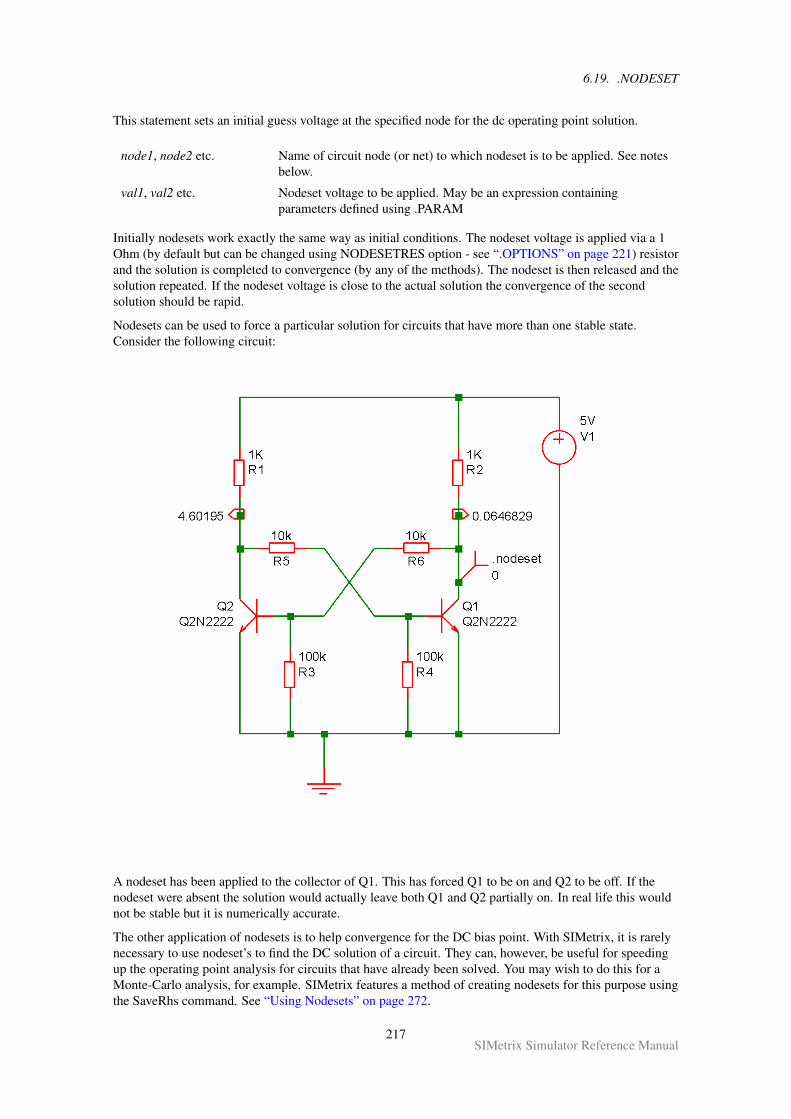
6.19. .NODESET
This statement sets an initial guess voltage at the specified node for the dc operating point solution.
node1, node2 etc. Name of circuit node (or net) to which nodeset is to be applied. See notesbelow.
val1, val2 etc. Nodeset voltage to be applied. May be an expression containingparameters defined using .PARAM
Initially nodesets work exactly the same way as initial conditions. The nodeset voltage is applied via a 1Ohm (by default but can be changed using NODESETRES option - see “.OPTIONS” on page 221) resistorand the solution is completed to convergence (by any of the methods). The nodeset is then released and thesolution repeated. If the nodeset voltage is close to the actual solution the convergence of the secondsolution should be rapid.
Nodesets can be used to force a particular solution for circuits that have more than one stable state.Consider the following circuit:
A nodeset has been applied to the collector of Q1. This has forced Q1 to be on and Q2 to be off. If thenodeset were absent the solution would actually leave both Q1 and Q2 partially on. In real life this wouldnot be stable but it is numerically accurate.
The other application of nodesets is to help convergence for the DC bias point. With SIMetrix, it is rarelynecessary to use nodeset’s to find the DC solution of a circuit. They can, however, be useful for speedingup the operating point analysis for circuits that have already been solved. You may wish to do this for aMonte-Carlo analysis, for example. SIMetrix features a method of creating nodesets for this purpose usingthe SaveRhs command. See “Using Nodesets” on page 272.
217SIMetrix Simulator Reference Manual
6.20. .NOISE
Nodeset’s should not be confused with initial conditions. (see “.IC” on page 205). Initial conditions tie anode to a particular voltage and keep it there throughout the DC operating point analysis. Nodesets merelysuggest a possible solution but do not force it.
6.20 .NOISE
.NOISE inner_sweep_spec [ V ] pos_node [ VN ] neg_node+ [[ INSRC ] in_source ]+ [ F frequency ] [RUNNAME=runname] [SWEEP outer_sweep_spec]
Spice Compatible:
.NOISE V(pos_node [, neg_out_node ]) in_source+ DEC|LIN|OCT num_points start stop interval
This statement instructs the simulator to perform a small signal noise analysis.
pos_node Node on circuit at which noise is measured.
neg_node Node to which outputnode is referenced. Defaults to ground ifomitted.
in_source Input source (i.e. voltage or current) to which the input noise measurementis referred.
inner_sweep_spec See “General Sweep Specification” on page 190 for syntax. Defines sweepmode. FREQ keyword is optional.
outer_sweep_spec If specified, analysis will be repeated according to this specification. See“General Sweep Specification” on page 190 for syntax.
LIN Analysis points are linearly spaced.
DEC Analysis points are logarithmically spaced in decades
OCT Analysis points are logarithmically spaced in octaves
num_pointsLIN: Total number of points
DEC: Number of points per decade
OCT: Number of points per octave
start Start frequency
stop Stop frequency
interval Currently does nothing. Provided for backward compatibility.
runname If specified, the value for runname will be passed to the simulation datagroup as a string variable with name UserRunName. This may be used toidentify which analysis generated the data which is useful when runningnetlists with multiple analyses defined
6.20.1 Notes
During noise analysis the simulator calculates the total noise measured between pos_node and neg_node ateach frequency point. It also calculates and outputs this noise referred back to an input specified byin_source. As for all other analysis modes a DC operating point analysis is carried out first but, unlike ACanalysis, the results of this analysis are not made available. The simulator outputs vectors covering thecontribution from each noise generating device to the total output noise. The names of these vectors begin
218SIMetrix Simulator Reference Manual
6.20. .NOISE
with the component reference of the device followed by a suffix to indicate the source of the noise withinthe device. A listing of the suffixes is given below. It is important to note that it is not the noise beinggenerated by each device that is output but the proportion of that noise that is propagated to the output.
It is not necessary to specify a separate AC analysis alongside the noise analysis as it is with SPICE2 andcommercial derivatives of SPICE2.
The magnitude of any AC independent voltage or current source on the circuit has no effect on the resultsof a noise analysis. Unlike SPICE and earlier versions of SIMetrix, it is not necessary to specify an ACparameter for the source used for the noise input source. For the first form shown above, the input sourceis in fact optional. If it is omitted the input referred noise will not be calculated.
All noise results are in V/√
Hz except input noise referred back to a current source which is in A/√
Hz. Instandard SPICE3 the noise values produced for MOS2 and BSIM3 devices are in V2/
√Hz. For
consistency, these have now been changed to V/√
Hz. The original SPICE3 behaviour can be restored bysetting the simulator option OldMosNoise (see “.OPTIONS” on page 221).
6.20.2 Device vector name suffixes
Device Type Suffix and Description
BJT #rc Noise due to collector resistance
#rb Noise due to base resistance
#re Noise due to emitter resistance
#ic Shot noise in collector
#ib Shot noise in base
#1overf Flicker (1/f) noise
no suffix Total transistor noise
Diode #rs Noise due to series resistance
#id Shot noise
#1overf Flicker (1/f) noise
no suffix Total diode noise
JFET and MOSFETs level 1-3 andBSIM3
#rd Noise due to drain resistance
#rs Noise due to source resistance
#id Shot noise in drain
#1overf Flicker (1/f) noise
no suffix Total FET noise
NXP MOS9 (all types see “NXPCompact Models” onpage 126)
#Sfl Flicker (1/f) noise
#Sth Drain thermal noise
#Sig Gate thermal noise
#Sigth Gate-drain correlated thermal noise
no suffix Total FET noise
Resistor #therm Resistor thermal noise
#1overf Flicker (1/f) noise
#noise Total resistor noise
219SIMetrix Simulator Reference Manual
6.21. .OP
Device Type Suffix and Description
Voltage controlled switch no suffix Total switch noise
6.20.3 Creating Noise Info File
Noise analysis generates vectors in the same way as all other swept analyses. Individual vectors may alsobe tabulated in the list file using the .PRINT statement.
A noise output file may also be created from the front end. Select the command shell menu Graphs andData | Create Noise Output File to create a text file with a summary of noise results. Included is a list ofthe integrated noise output for every device listed in order of magnitude. Select Graphs and Data | ViewNoise Output File to view the file. Note that this is a front end feature and is not implemented by thesimulator.
6.20.4 Examples
Run noise analysis from 100Hz to 1MHz with 25 points per decade. Calculate noise at node named voutand noise referred back to voltage source vin:
.NOISE V( vout ) vin dec 25 100 1meg
Decade sweep resistor RSource from 100 to 10K with 25 points per decade. Frequency = 1kHz
.NOISE DEVICE RSource DEC 25 100 10k F=1K
6.21 .OP
.OP
This statement instructs the simulator to perform a DC operating point analysis. Note that a DC operatingpoint analysis is carried out automatically for transient (unless the UIC parameter is specified), AC, DC,transfer function and noise analyses.
DC operating point analysis attempts to find a stable bias point for the circuit. It does this by first applyingan initial guess and then uses an iterative algorithm to converge on a solution. If it fails to find a solutionby this method the simulator then attempts three further strategies.
For the first, a method known as ‘source stepping’ is employed. For this all voltage and current sources inthe circuit are initially set to near zero and the solution found. The sources are then gradually increaseduntil they reach their final value.
If this approach fails a second strategy ‘GMIN stepping’ is invoked. This conditions the solution matrix byincreasing the diagonal term such that it is dominant. If large enough, convergence is virtually guaranteed.If successful then the diagonal term is reduced and a further solution sought using the previous solution asa starting point. This procedure is repeated until the diagonal term is returned to its correct value.Increasing the diagonal term is in a way similar, but by no means identical, to placing a small resistance ateach node of the circuit.
If source stepping fails a final strategy, ‘pseudo transient analysis’ is invoked. This is the most powerfultechnique employed and nearly always succeeds. However, it is also the slowest which is why it is leftuntil last. For more information on DC convergence see “Convergence, Accuracy and Performance” onpage 268.
220SIMetrix Simulator Reference Manual
6.22. .OPTIONS
If the final approach fails then the analysis will abort.
IMPORTANT: It is not necessary to include .OP if other analyses are specified. All other analysis modeswill perform an operating point anyway so including .OP will simply cause it to be done twice. However,with .NOISE, .TF, .SENS and .PZ the results of the operating point analysis are not output. If the biaspoint of the circuit is required when running one of these analysis modes, a .OP will be needed.
6.21.1 ‘OFF’ Parameters
Some semiconductor devices feature the device parameter OFF. If there are devices in the circuit whichspecify this parameter, the bias point solution is found in two stages. In stage 1 the devices with OFFspecified are treated as if their output terminals are open circuit and the operating point algorithmcompletes to convergence. In stage 2, The OFF state is then released and the solution restarted butinitialised with the results of stage 1.
The result of this procedure is that OFF devices that are part of latching circuits are induced to be in theOFF state. Note that the OFF parameter only affects circuits that have more than one possible DC solutionsuch as bistables. If the OFF parameter is specified in - say - an amplifier circuit - with a unique solution,the final result will be the same. It will just take a little longer to arrive at it.
6.21.2 Nodesets
Nodesets work in a similar way to the OFF parameter in that the solution is found in two stages. In the firstthe nodeset is applied and the solution found. It is then released and convergence continues. Nodeset arean aid to convergence and, like the OFF parameter, can coerce a particular solution if there is more than 1stable state. See “.NODESET” on page 216 for details.
6.21.3 Initial Conditions
Initial conditions force a particular voltage at a circuit node during bias point solution. The force isreleased for any subsequent analysis. See “.IC” on page 205 for more details.
6.21.4 Operating Point Output Info
During the operating point analysis, operating point values of every device in the circuit are output to thelist file (see “The List File” on page 11). This information is not usually output for other analysis modesunless explicitly requested. The output of operating point information is controlled by three simulatoroptions:
NOOPINFO If set, the operating point info file is not created for .OP analysis
OPINFO If set, the operating point info file is created for other analyses as well as.OP. (Does not apply to .SENS - operating point information is notavailable for this mode at all)
OPINFOFILE Sets name of file to receive operating point info. Outputs to list file if thisoption is not specified.
6.22 .OPTIONS
.OPTIONS [ opt1 [=val1]] ...
This statement allows the setting of various options specific to the simulator.
221SIMetrix Simulator Reference Manual
6.22. .OPTIONS
opt1 Option name. Must be one specified in list below.
val1 Option value. Note, boolean options do not have a value. They areassigned “true” if the name is present and “false” if not.
6.22.1 List of simulator options
Option name Defaultvalue
Description
ABSTOL 1p Units = A The absolute current errortolerance. It is sometimes desirableto increase this for circuits that carrylarge currents (>1A) to speed thesolution and aid convergence.
ACCT false Full simulation timing statistics aregenerated if this is enabled.
ADVCONVREPORT false Enables advanced convergencereporting. Information from this canbe retrieved using the script functionGetNodeConvergenceInfo()
ALLACI false Instructs simulator to save all devicecurrents in an AC analysis. Usually,only currents for simple devices areevaluated and stored. Equivalent to“.KEEP /allaci”, but unlike .KEEP,.OPTIONS values can be defined onthe Run command line.
ALLOWDIVZERO 0 Set to 1 to allow division by constantzero in arbitrary source expressions.The result of dividing by zero whenenabled will be 1e30 for positivenumbers, -1e30 for negative numbersand 0 for 0. If not enabled, a divisionby zero will lead to an error and thesimulation will abort. This optiononly affects division by a constantvalue of zero and does not apply tocircuit variables. For example 1/awhere a is a parameter that is zerowill return 1e30. Conversely1/V (n1) when node n1 reaches zerois not affected by this option setting.This option is automatically set to 1if the optionPSPICECOMPATIBILITY is set to 1or higher.
ANYVERSION false If true, version dependent modelssuch as BSIM3 and BSIM4 will beunconditionally accepted even if aninvalid version parameter issupplied.
222SIMetrix Simulator Reference Manual
6.22. .OPTIONS
Option name Defaultvalue
Description
BINDIAG false If enabled, a report about selection ofbinned models will be output to thelist file. See “Model Binning” onpage 32.
CHGTOL 1e-14 Units = Coulombs The absolutecharge tolerance.
CONV 0 Set to a value from 0 to 8. See“Iteration Modes” on page 273 formore information
CSHUNT 0 Units = Farads. Capacitance placedat all top level nodes to ground. IfCSHUNTSUB specified, capacitanceis placed at all nodes in the circuit.No capacitance is placed to nodesthat already have a capacitorconnected to ground. By placing asmall capacitance at every node,some transient analysis convergenceproblems can be solved. A verysmall value such as 100fF can oftenbe effective
CSHUNTSUB false Boolean. If specified CSHUNTplaces capacitance to all nodes, notjust those at the top level. Thisshould be used with care if used incircuits with subcircuit modelsobtained from third-party vendors.Some have very high impedanceinternal nodes and their behaviourcan be adversely affected by evenvery small additionalcapacitance.
DCOPSEQUENCE gmin|source|pta
Operating point strategy sequenceorder. See “Controlling DC MethodSequence” on page 277 fordetails
DEFAD 0 Unit = m2
Default value for MOSFET ADdevice parameter. Applies to levels1-3 and level 49/53. Does not applyto level 8 or NXP MOS9devices
DEFAS 0 Unit = m2
As DEFAD but for ASparameter
DEFL 100µ Unit = metres As DEFAD but for Lparameter
223SIMetrix Simulator Reference Manual
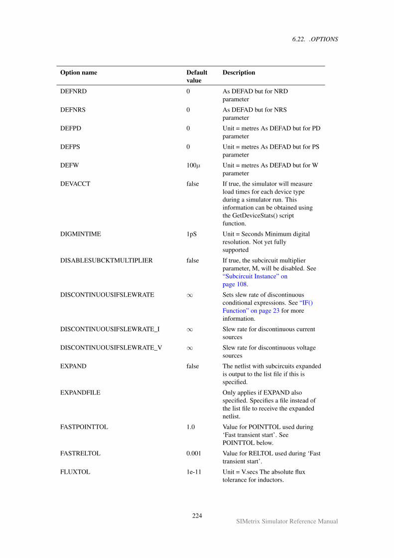
6.22. .OPTIONS
Option name Defaultvalue
Description
DEFNRD 0 As DEFAD but for NRDparameter
DEFNRS 0 As DEFAD but for NRSparameter
DEFPD 0 Unit = metres As DEFAD but for PDparameter
DEFPS 0 Unit = metres As DEFAD but for PSparameter
DEFW 100µ Unit = metres As DEFAD but for Wparameter
DEVACCT false If true, the simulator will measureload times for each device typeduring a simulator run. Thisinformation can be obtained usingthe GetDeviceStats() scriptfunction.
DIGMINTIME 1pS Unit = Seconds Minimum digitalresolution. Not yet fullysupported
DISABLESUBCKTMULTIPLIER false If true, the subcircuit multiplierparameter, M, will be disabled. See“Subcircuit Instance” onpage 108.
DISCONTINUOUSIFSLEWRATE ∞ Sets slew rate of discontinuousconditional expressions. See “IF()Function” on page 23 for moreinformation.
DISCONTINUOUSIFSLEWRATE_I ∞ Slew rate for discontinuous currentsources
DISCONTINUOUSIFSLEWRATE_V ∞ Slew rate for discontinuous voltagesources
EXPAND false The netlist with subcircuits expandedis output to the list file if this isspecified.
EXPANDFILE Only applies if EXPAND alsospecified. Specifies a file instead ofthe list file to receive the expandednetlist.
FASTPOINTTOL 1.0 Value for POINTTOL used during‘Fast transient start’. SeePOINTTOL below.
FASTRELTOL 0.001 Value for RELTOL used during ‘Fasttransient start’.
FLUXTOL 1e-11 Unit = V.secs The absolute fluxtolerance for inductors.
224SIMetrix Simulator Reference Manual
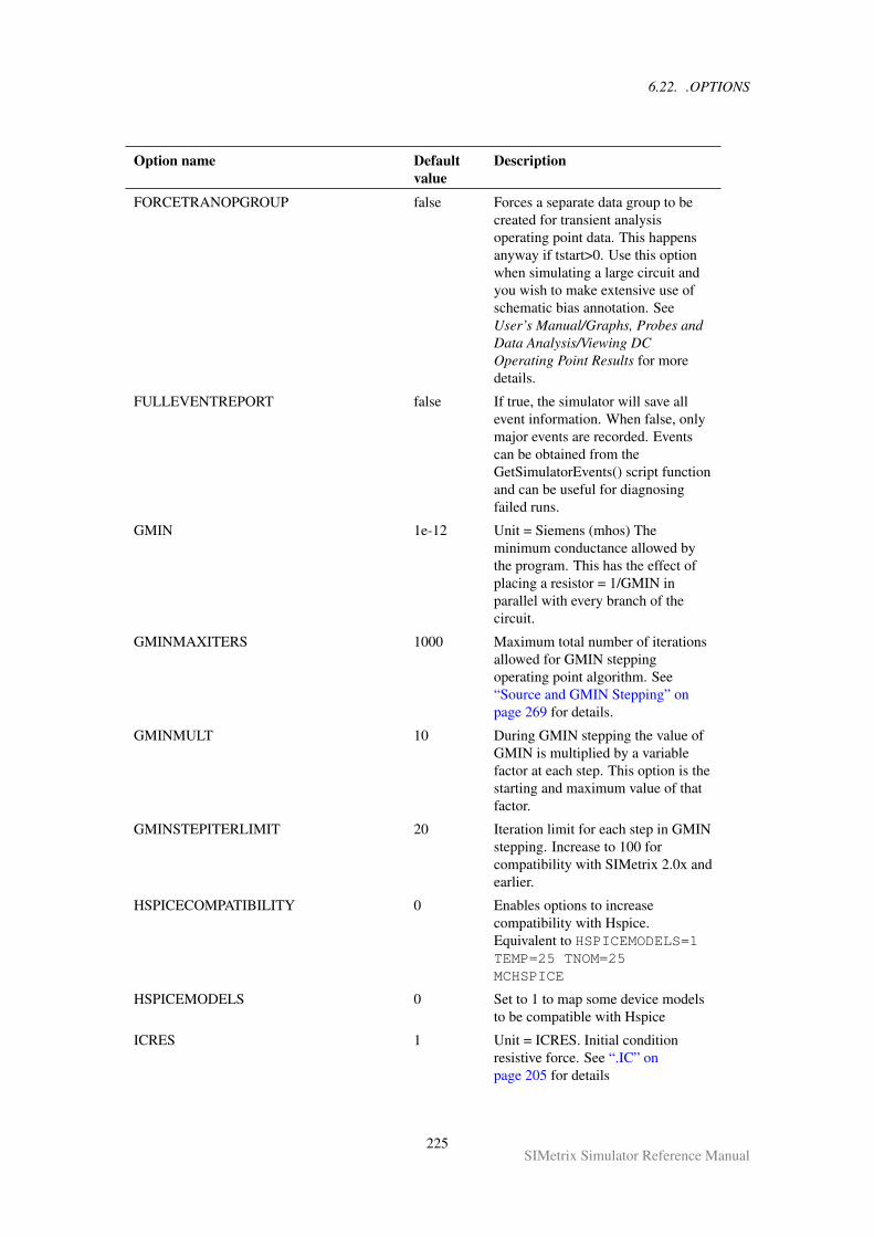
6.22. .OPTIONS
Option name Defaultvalue
Description
FORCETRANOPGROUP false Forces a separate data group to becreated for transient analysisoperating point data. This happensanyway if tstart>0. Use this optionwhen simulating a large circuit andyou wish to make extensive use ofschematic bias annotation. SeeUser’s Manual/Graphs, Probes andData Analysis/Viewing DCOperating Point Results for moredetails.
FULLEVENTREPORT false If true, the simulator will save allevent information. When false, onlymajor events are recorded. Eventscan be obtained from theGetSimulatorEvents() script functionand can be useful for diagnosingfailed runs.
GMIN 1e-12 Unit = Siemens (mhos) Theminimum conductance allowed bythe program. This has the effect ofplacing a resistor = 1/GMIN inparallel with every branch of thecircuit.
GMINMAXITERS 1000 Maximum total number of iterationsallowed for GMIN steppingoperating point algorithm. See“Source and GMIN Stepping” onpage 269 for details.
GMINMULT 10 During GMIN stepping the value ofGMIN is multiplied by a variablefactor at each step. This option is thestarting and maximum value of thatfactor.
GMINSTEPITERLIMIT 20 Iteration limit for each step in GMINstepping. Increase to 100 forcompatibility with SIMetrix 2.0x andearlier.
HSPICECOMPATIBILITY 0 Enables options to increasecompatibility with Hspice.Equivalent to HSPICEMODELS=1TEMP=25 TNOM=25MCHSPICE
HSPICEMODELS 0 Set to 1 to map some device modelsto be compatible with Hspice
ICRES 1 Unit = ICRES. Initial conditionresistive force. See “.IC” onpage 205 for details
225SIMetrix Simulator Reference Manual
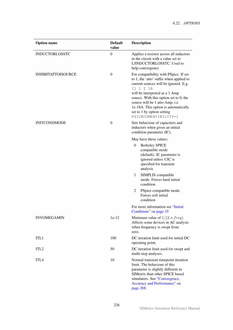
6.22. .OPTIONS
Option name Defaultvalue
Description
INDUCTORLOSSTC 0 Applies a resistor across all inductorsin the circuit with a value set toL/INDUCTORLOSSTC. Used tohelp convergence
INHIBITATTOISOURCE 0 For compatibility with PSpice. If setto 1, the ‘atto’ suffix when applied tocurrent sources will be ignored. E.g.I1 1 2 1Awill be interpreted as a 1 Ampsource. With this option set to 0, thesource will be 1 atto-Amp, i.e.1e-18A. This option is automaticallyset to 1 by option settingPSICECOMPATIBILITY=1
INITCONDMODE 0 Sets behaviour of capacitors andinductors when given an initialcondition parameter (IC).
May have these values:
0 Berkeley SPICEcompatible mode(default). IC parameter isignored unless UIC isspecified for transientanalysis
1 SIMPLIS compatiblemode. Forces hard initialcondition
2 PSpice compatible mode.Forces soft initialcondition
For more information see “InitialConditions” on page 35
INVOMEGAMIN 1e-12 Minimum value of 1/(2.π.freq).Affects some devices in AC analysiswhen frequency is swept fromzero.
ITL1 100 DC iteration limit used for initial DCoperating point.
ITL2 50 DC iteration limit used for swept andmulti-step analyses.
ITL4 10 Normal transient timepoint iterationlimit. The behaviour of thisparameter is slightly different inSIMetrix than other SPICE basedsimulators. See “Convergence,Accuracy and Performance” onpage 268.
226SIMetrix Simulator Reference Manual
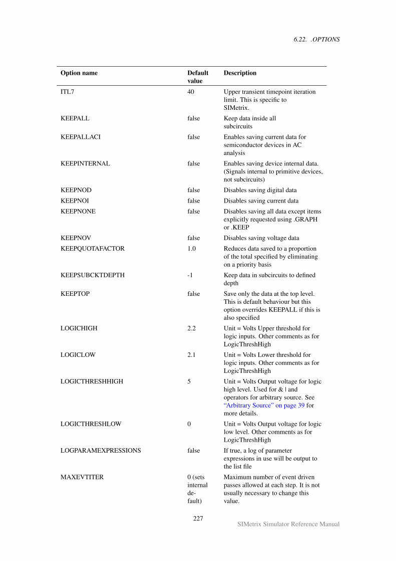
6.22. .OPTIONS
Option name Defaultvalue
Description
ITL7 40 Upper transient timepoint iterationlimit. This is specific toSIMetrix.
KEEPALL false Keep data inside allsubcircuits
KEEPALLACI false Enables saving current data forsemiconductor devices in ACanalysis
KEEPINTERNAL false Enables saving device internal data.(Signals internal to primitive devices,not subcircuits)
KEEPNOD false Disables saving digital data
KEEPNOI false Disables saving current data
KEEPNONE false Disables saving all data except itemsexplicitly requested using .GRAPHor .KEEP
KEEPNOV false Disables saving voltage data
KEEPQUOTAFACTOR 1.0 Reduces data saved to a proportionof the total specified by eliminatingon a priority basis
KEEPSUBCKTDEPTH -1 Keep data in subcircuits to defineddepth
KEEPTOP false Save only the data at the top level.This is default behaviour but thisoption overrides KEEPALL if this isalso specified
LOGICHIGH 2.2 Unit = Volts Upper threshold forlogic inputs. Other comments as forLogicThreshHigh
LOGICLOW 2.1 Unit = Volts Lower threshold forlogic inputs. Other comments as forLogicThreshHigh
LOGICTHRESHHIGH 5 Unit = Volts Output voltage for logichigh level. Used for & | andoperators for arbitrary source. See“Arbitrary Source” on page 39 formore details.
LOGICTHRESHLOW 0 Unit = Volts Output voltage for logiclow level. Other comments as forLogicThreshHigh
LOGPARAMEXPRESSIONS false If true, a log of parameterexpressions in use will be output tothe list file
MAXEVTITER 0 (setsinternalde-fault)
Maximum number of event drivenpasses allowed at each step. It is notusually necessary to change thisvalue.
227SIMetrix Simulator Reference Manual
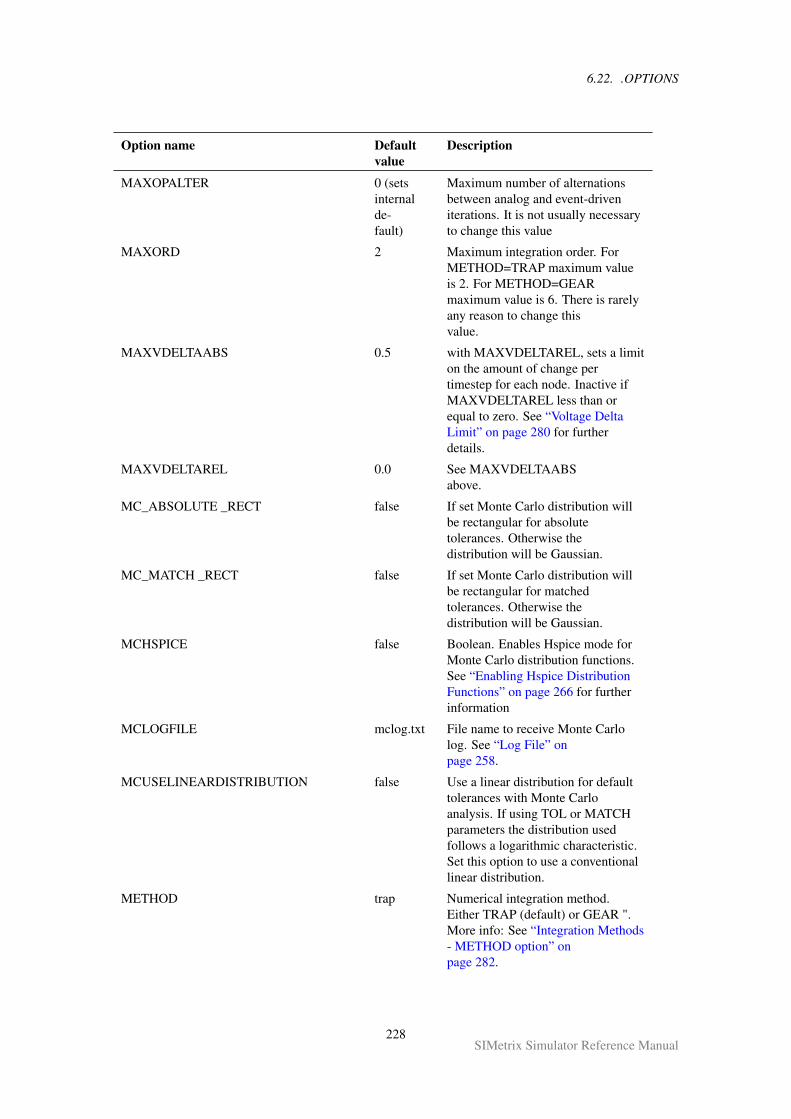
6.22. .OPTIONS
Option name Defaultvalue
Description
MAXOPALTER 0 (setsinternalde-fault)
Maximum number of alternationsbetween analog and event-driveniterations. It is not usually necessaryto change this value
MAXORD 2 Maximum integration order. ForMETHOD=TRAP maximum valueis 2. For METHOD=GEARmaximum value is 6. There is rarelyany reason to change thisvalue.
MAXVDELTAABS 0.5 with MAXVDELTAREL, sets a limiton the amount of change pertimestep for each node. Inactive ifMAXVDELTAREL less than orequal to zero. See “Voltage DeltaLimit” on page 280 for furtherdetails.
MAXVDELTAREL 0.0 See MAXVDELTAABSabove.
MC_ABSOLUTE _RECT false If set Monte Carlo distribution willbe rectangular for absolutetolerances. Otherwise thedistribution will be Gaussian.
MC_MATCH _RECT false If set Monte Carlo distribution willbe rectangular for matchedtolerances. Otherwise thedistribution will be Gaussian.
MCHSPICE false Boolean. Enables Hspice mode forMonte Carlo distribution functions.See “Enabling Hspice DistributionFunctions” on page 266 for furtherinformation
MCLOGFILE mclog.txt File name to receive Monte Carlolog. See “Log File” onpage 258.
MCUSELINEARDISTRIBUTION false Use a linear distribution for defaulttolerances with Monte Carloanalysis. If using TOL or MATCHparameters the distribution usedfollows a logarithmic characteristic.Set this option to use a conventionallinear distribution.
METHOD trap Numerical integration method.Either TRAP (default) or GEAR ".More info: See “Integration Methods- METHOD option” onpage 282.
228SIMetrix Simulator Reference Manual
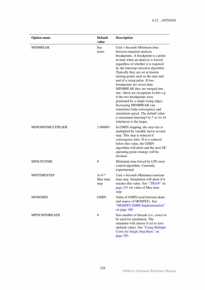
6.22. .OPTIONS
Option name Defaultvalue
Description
MINBREAK Seenotes
Unit = Seconds Minimum timebetween transient analysisbreakpoints. A breakpoint is a pointin time when an analysis is forcedregardless of whether it is requiredby the timestep selection algorithm.Typically they are set at knownturning points such as the start andend of a rising pulse. If twobreakpoints are closer thanMINBREAK they are merged intoone. (there are exceptions to this e.gif the two breakpoints weregenerated by a single rising edge).Increasing MINBREAK cansometimes help convergence andsimulation speed. The default valueis maximum-timestep*1e-7 or 1e-14whichever is the larger.
MINGMINMULTIPLIER 1.000001 In GMIN stepping, the step size ismultiplied by variable factor at eachstep. This step is reduced ifconvergence fails. If it is reducedbelow this value, the GMINalgorithm will abort and the next DCoperating point strategy will beinvoked.
MINLTETIME 0 Minimum time forced by LTE errorcontrol algorithm. Currentlyexperimental
MINTIMESTEP 1e-9 *Max timestep
Unit = Seconds Minimum transienttime step. Simulation will abort if itreaches this value. See “.TRAN” onpage 251 for value of Max timestep.
MOSGMIN GMIN Value of GMIN used between drainand source of MOSFETs. See“MOSFET GMIN Implementation”on page 100.
MPNUMTHREADS 0 Sets number of threads (i.e. cores) tobe used for simulation. Thesimulator will choose if set to zero(default value). See “Using MultipleCores for Single Step Runs” onpage 285.
229SIMetrix Simulator Reference Manual
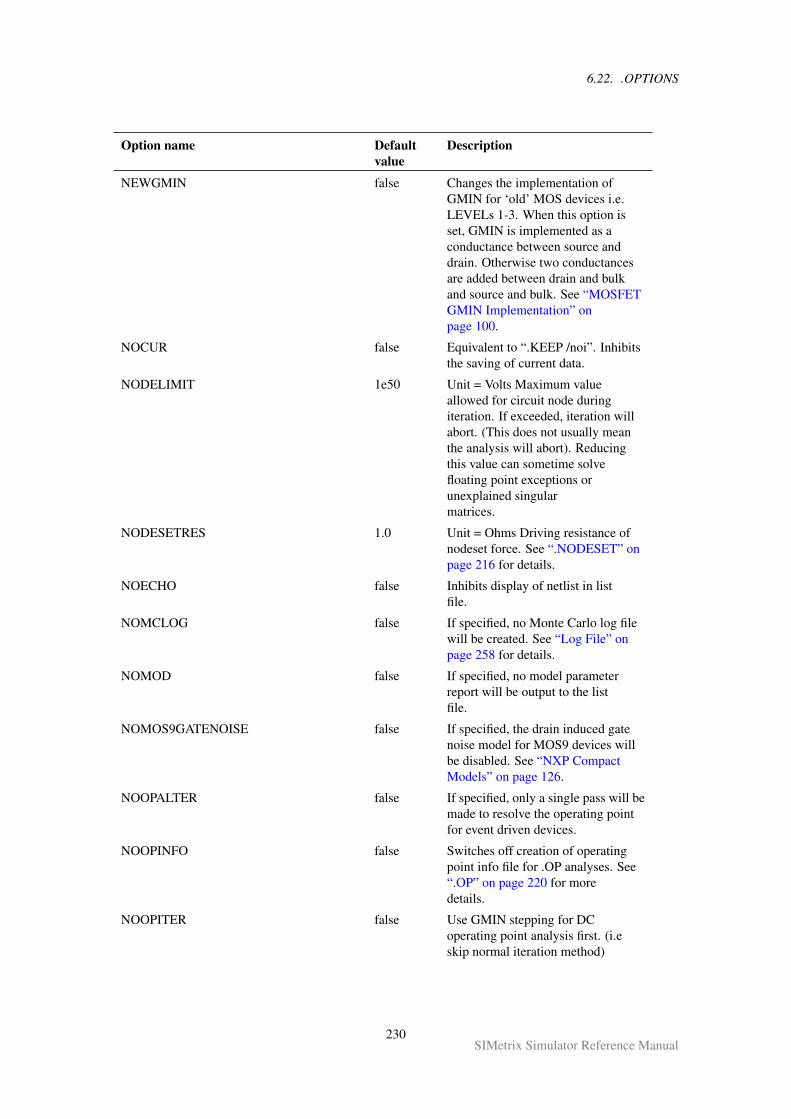
6.22. .OPTIONS
Option name Defaultvalue
Description
NEWGMIN false Changes the implementation ofGMIN for ‘old’ MOS devices i.e.LEVELs 1-3. When this option isset, GMIN is implemented as aconductance between source anddrain. Otherwise two conductancesare added between drain and bulkand source and bulk. See “MOSFETGMIN Implementation” onpage 100.
NOCUR false Equivalent to “.KEEP /noi”. Inhibitsthe saving of current data.
NODELIMIT 1e50 Unit = Volts Maximum valueallowed for circuit node duringiteration. If exceeded, iteration willabort. (This does not usually meanthe analysis will abort). Reducingthis value can sometime solvefloating point exceptions orunexplained singularmatrices.
NODESETRES 1.0 Unit = Ohms Driving resistance ofnodeset force. See “.NODESET” onpage 216 for details.
NOECHO false Inhibits display of netlist in listfile.
NOMCLOG false If specified, no Monte Carlo log filewill be created. See “Log File” onpage 258 for details.
NOMOD false If specified, no model parameterreport will be output to the listfile.
NOMOS9GATENOISE false If specified, the drain induced gatenoise model for MOS9 devices willbe disabled. See “NXP CompactModels” on page 126.
NOOPALTER false If specified, only a single pass will bemade to resolve the operating pointfor event driven devices.
NOOPINFO false Switches off creation of operatingpoint info file for .OP analyses. See“.OP” on page 220 for moredetails.
NOOPITER false Use GMIN stepping for DCoperating point analysis first. (i.eskip normal iteration method)
230SIMetrix Simulator Reference Manual
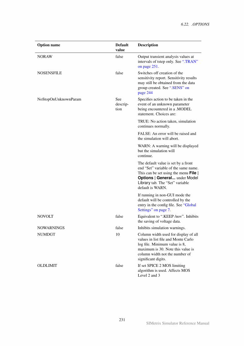
6.22. .OPTIONS
Option name Defaultvalue
Description
NORAW false Output transient analysis values atintervals of tstep only. See “.TRAN”on page 251.
NOSENSFILE false Switches off creation of thesensitivity report. Sensitivity resultsmay still be obtained from the datagroup created. See “.SENS” onpage 244
NoStopOnUnknownParam Seedescrip-tion
Specifies action to be taken in theevent of an unknown parameterbeing encountered in a .MODELstatement. Choices are:
TRUE: No action taken, simulationcontinues normally.
FALSE: An error will be raised andthe simulation will abort.
WARN: A warning will be displayedbut the simulation willcontinue.
The default value is set by a frontend “Set” variable of the same name.This can be set using the menu File |Options | General... under ModelLibrary tab. The “Set” variabledefault is WARN.
If running in non-GUI mode thedefault will be controlled by theentry in the config file. See “GlobalSettings” on page 7.
NOVOLT false Equivalent to “.KEEP /nov”. Inhibitsthe saving of voltage data.
NOWARNINGS false Inhibits simulation warnings.
NUMDGT 10 Column width used for display of allvalues in list file and Monte Carlolog file. Minimum value is 8,maximum is 30. Note this value iscolumn width not the number ofsignificant digits.
OLDLIMIT false If set SPICE 2 MOS limitingalgorithm is used. Affects MOSLevel 2 and 3
231SIMetrix Simulator Reference Manual
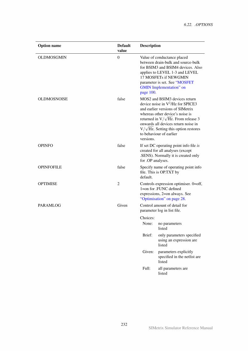
6.22. .OPTIONS
Option name Defaultvalue
Description
OLDMOSGMIN 0 Value of conductance placedbetween drain-bulk and source-bulkfor BSIM3 and BSIM4 devices. Alsoapplies to LEVEL 1-3 and LEVEL17 MOSFETs if NEWGMINparameter is set. See “MOSFETGMIN Implementation” onpage 100.
OLDMOSNOISE false MOS2 and BSIM3 devices returndevice noise in V2/Hz for SPICE3and earlier versions of SIMetrixwhereas other device’s noise isreturned in V/
√Hz. From release 3
onwards all devices return noise inV/√
Hz. Setting this option restoresto behaviour of earlierversions.
OPINFO false If set DC operating point info file iscreated for all analyses (except.SENS). Normally it is created onlyfor .OP analyses.
OPINFOFILE false Specify name of operating point infofile. This is OP.TXT bydefault.
OPTIMISE 2 Controls expression optimiser. 0=off,1=on for .FUNC definedexpressions, 2=on always. See“Optimisation” on page 28.
PARAMLOG Given Control amount of detail forparameter log in list file.
Choices:None: no parameters
listed
Brief: only parameters specifiedusing an expression arelisted
Given: parameters explicitlyspecified in the netlist arelisted
Full: all parameters arelisted
232SIMetrix Simulator Reference Manual
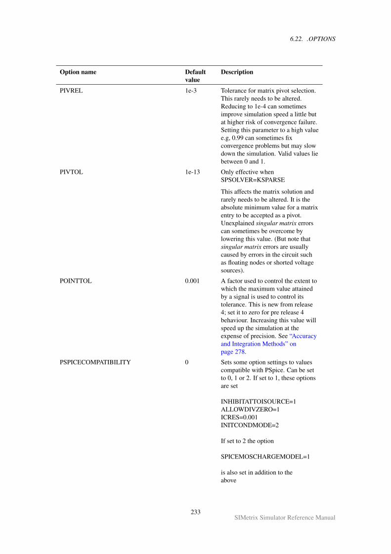
6.22. .OPTIONS
Option name Defaultvalue
Description
PIVREL 1e-3 Tolerance for matrix pivot selection.This rarely needs to be altered.Reducing to 1e-4 can sometimesimprove simulation speed a little butat higher risk of convergence failure.Setting this parameter to a high valuee.g, 0.99 can sometimes fixconvergence problems but may slowdown the simulation. Valid values liebetween 0 and 1.
PIVTOL 1e-13 Only effective whenSPSOLVER=KSPARSE
This affects the matrix solution andrarely needs to be altered. It is theabsolute minimum value for a matrixentry to be accepted as a pivot.Unexplained singular matrix errorscan sometimes be overcome bylowering this value. (But note thatsingular matrix errors are usuallycaused by errors in the circuit suchas floating nodes or shorted voltagesources).
POINTTOL 0.001 A factor used to control the extent towhich the maximum value attainedby a signal is used to control itstolerance. This is new from release4; set it to zero for pre release 4behaviour. Increasing this value willspeed up the simulation at theexpense of precision. See “Accuracyand Integration Methods” onpage 278.
PSPICECOMPATIBILITY 0 Sets some option settings to valuescompatible with PSpice. Can be setto 0, 1 or 2. If set to 1, these optionsare set
INHIBITATTOISOURCE=1ALLOWDIVZERO=1ICRES=0.001INITCONDMODE=2
If set to 2 the option
SPICEMOSCHARGEMODEL=1
is also set in addition to theabove
233SIMetrix Simulator Reference Manual
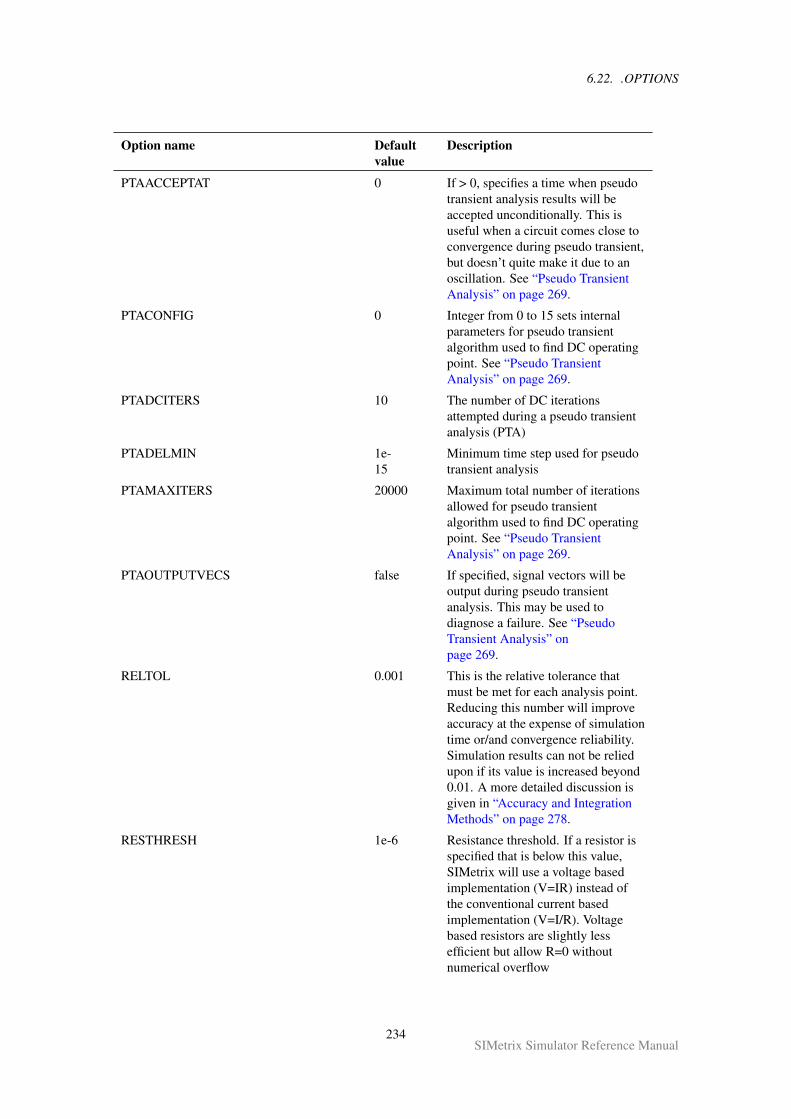
6.22. .OPTIONS
Option name Defaultvalue
Description
PTAACCEPTAT 0 If > 0, specifies a time when pseudotransient analysis results will beaccepted unconditionally. This isuseful when a circuit comes close toconvergence during pseudo transient,but doesn’t quite make it due to anoscillation. See “Pseudo TransientAnalysis” on page 269.
PTACONFIG 0 Integer from 0 to 15 sets internalparameters for pseudo transientalgorithm used to find DC operatingpoint. See “Pseudo TransientAnalysis” on page 269.
PTADCITERS 10 The number of DC iterationsattempted during a pseudo transientanalysis (PTA)
PTADELMIN 1e-15
Minimum time step used for pseudotransient analysis
PTAMAXITERS 20000 Maximum total number of iterationsallowed for pseudo transientalgorithm used to find DC operatingpoint. See “Pseudo TransientAnalysis” on page 269.
PTAOUTPUTVECS false If specified, signal vectors will beoutput during pseudo transientanalysis. This may be used todiagnose a failure. See “PseudoTransient Analysis” onpage 269.
RELTOL 0.001 This is the relative tolerance thatmust be met for each analysis point.Reducing this number will improveaccuracy at the expense of simulationtime or/and convergence reliability.Simulation results can not be reliedupon if its value is increased beyond0.01. A more detailed discussion isgiven in “Accuracy and IntegrationMethods” on page 278.
RESTHRESH 1e-6 Resistance threshold. If a resistor isspecified that is below this value,SIMetrix will use a voltage basedimplementation (V=IR) instead ofthe conventional current basedimplementation (V=I/R). Voltagebased resistors are slightly lessefficient but allow R=0 withoutnumerical overflow
234SIMetrix Simulator Reference Manual
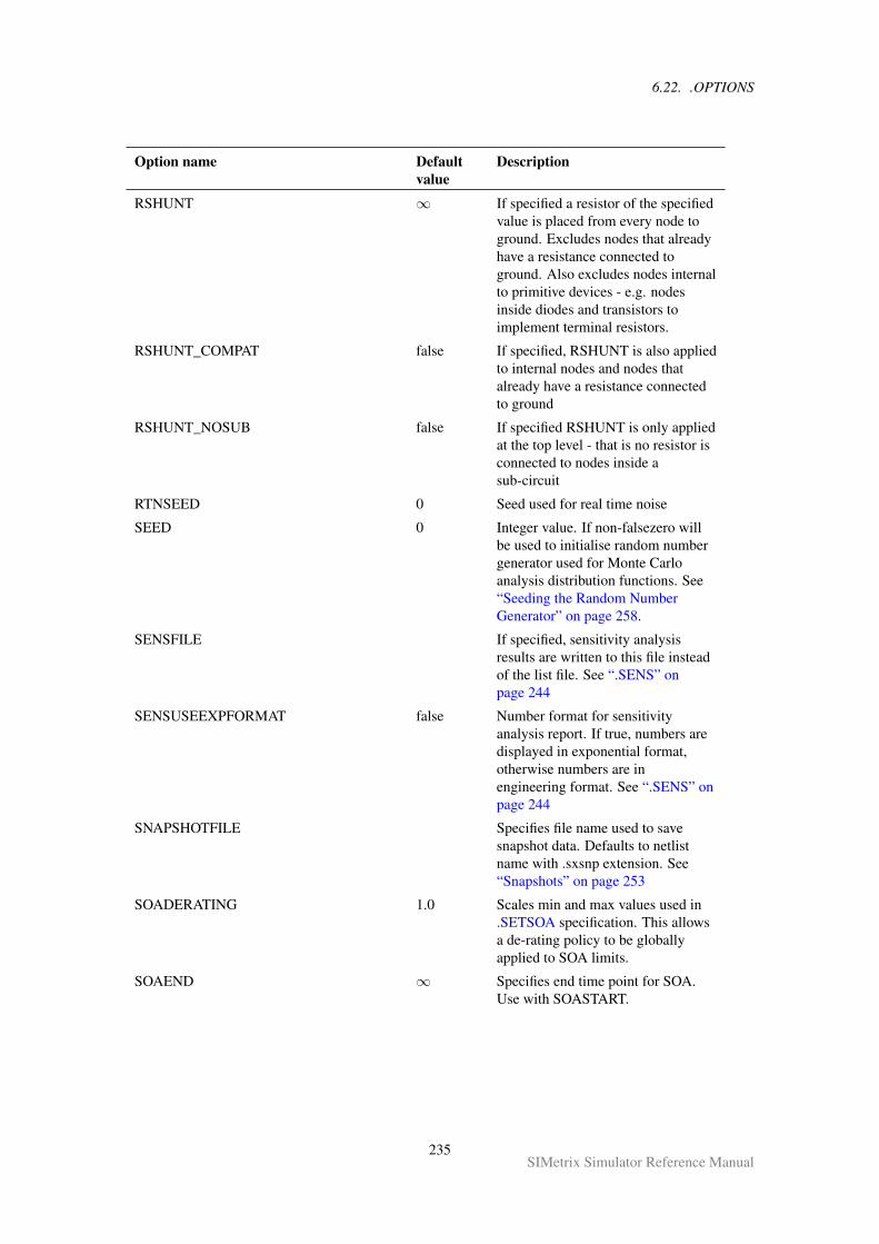
6.22. .OPTIONS
Option name Defaultvalue
Description
RSHUNT ∞ If specified a resistor of the specifiedvalue is placed from every node toground. Excludes nodes that alreadyhave a resistance connected toground. Also excludes nodes internalto primitive devices - e.g. nodesinside diodes and transistors toimplement terminal resistors.
RSHUNT_COMPAT false If specified, RSHUNT is also appliedto internal nodes and nodes thatalready have a resistance connectedto ground
RSHUNT_NOSUB false If specified RSHUNT is only appliedat the top level - that is no resistor isconnected to nodes inside asub-circuit
RTNSEED 0 Seed used for real time noise
SEED 0 Integer value. If non-falsezero willbe used to initialise random numbergenerator used for Monte Carloanalysis distribution functions. See“Seeding the Random NumberGenerator” on page 258.
SENSFILE If specified, sensitivity analysisresults are written to this file insteadof the list file. See “.SENS” onpage 244
SENSUSEEXPFORMAT false Number format for sensitivityanalysis report. If true, numbers aredisplayed in exponential format,otherwise numbers are inengineering format. See “.SENS” onpage 244
SNAPSHOTFILE Specifies file name used to savesnapshot data. Defaults to netlistname with .sxsnp extension. See“Snapshots” on page 253
SOADERATING 1.0 Scales min and max values used in.SETSOA specification. This allowsa de-rating policy to be globallyapplied to SOA limits.
SOAEND ∞ Specifies end time point for SOA.Use with SOASTART.
235SIMetrix Simulator Reference Manual
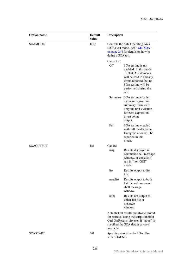
6.22. .OPTIONS
Option name Defaultvalue
Description
SOAMODE false Controls the Safe Operating Area(SOA) test mode. See “.SETSOA”on page 244 for details on how todefine a SOA test.
Can set to:Off SOA testing is not
enabled. In this mode.SETSOA statementswill be read in and anyerrors reported, but noSOA testing will beperformed during therun.
Summary SOA testing enabledand results given insummary form withonly the first violationfor each expressiongiven beingoutput.
Full SOA testing enabledwith full results given.Every violation will bereported in thismode.
SOAOUTPUT list Can be:msg Results displayed in
command shell messagewindow, or console ifrun in “non-GUI”mode.
list Results output to listfile.
msg|list Results output to bothlist file and commandshell messagewindow.
none Results not output toeither list file ormessagewindow.
Note that all results are always storedfor retrieval using the script functionGetSOAResults. So even if “none” isspecified the SOA data is alwaysavailable.
SOASTART 0.0 Specifies start time for SOA. Usewith SOAEND
236SIMetrix Simulator Reference Manual
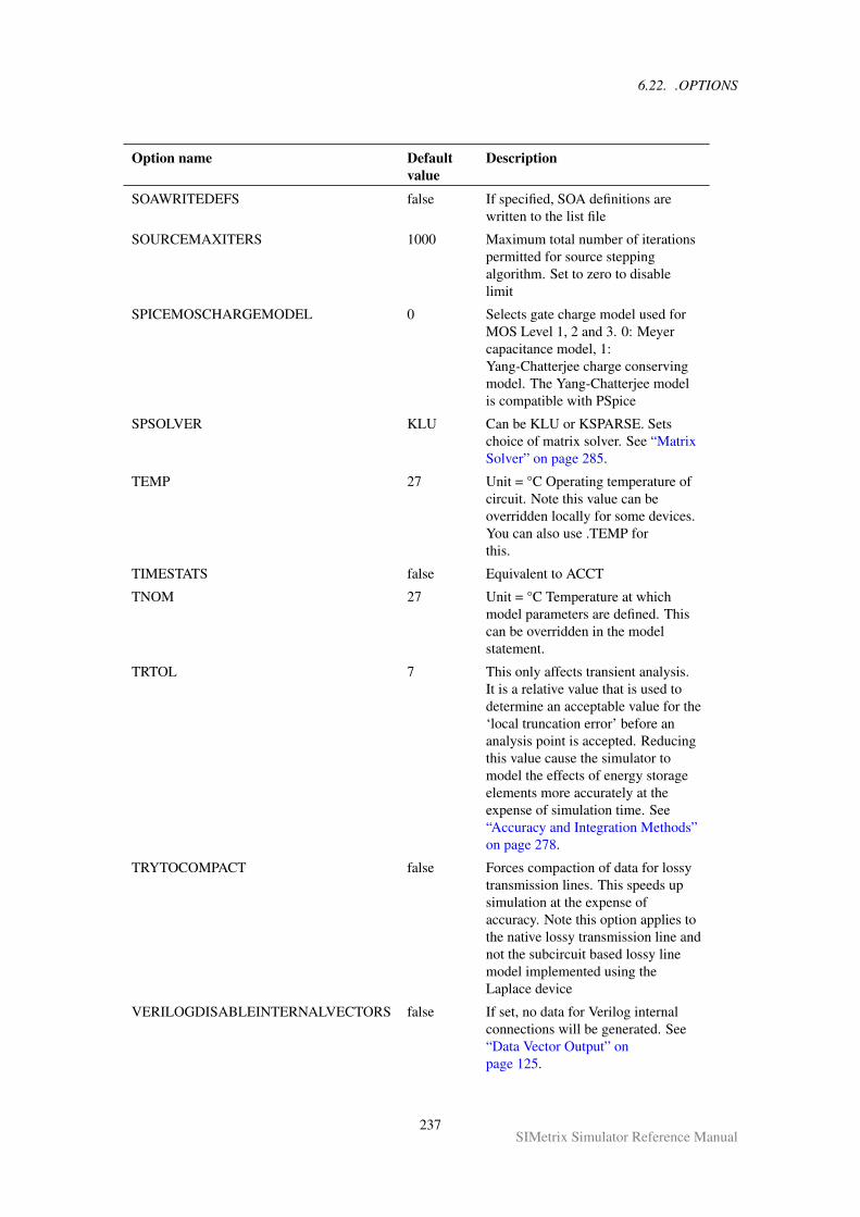
6.22. .OPTIONS
Option name Defaultvalue
Description
SOAWRITEDEFS false If specified, SOA definitions arewritten to the list file
SOURCEMAXITERS 1000 Maximum total number of iterationspermitted for source steppingalgorithm. Set to zero to disablelimit
SPICEMOSCHARGEMODEL 0 Selects gate charge model used forMOS Level 1, 2 and 3. 0: Meyercapacitance model, 1:Yang-Chatterjee charge conservingmodel. The Yang-Chatterjee modelis compatible with PSpice
SPSOLVER KLU Can be KLU or KSPARSE. Setschoice of matrix solver. See “MatrixSolver” on page 285.
TEMP 27 Unit = °C Operating temperature ofcircuit. Note this value can beoverridden locally for some devices.You can also use .TEMP forthis.
TIMESTATS false Equivalent to ACCT
TNOM 27 Unit = °C Temperature at whichmodel parameters are defined. Thiscan be overridden in the modelstatement.
TRTOL 7 This only affects transient analysis.It is a relative value that is used todetermine an acceptable value for the‘local truncation error’ before ananalysis point is accepted. Reducingthis value cause the simulator tomodel the effects of energy storageelements more accurately at theexpense of simulation time. See“Accuracy and Integration Methods”on page 278.
TRYTOCOMPACT false Forces compaction of data for lossytransmission lines. This speeds upsimulation at the expense ofaccuracy. Note this option applies tothe native lossy transmission line andnot the subcircuit based lossy linemodel implemented using theLaplace device
VERILOGDISABLEINTERNALVECTORS false If set, no data for Verilog internalconnections will be generated. See“Data Vector Output” onpage 125.
237SIMetrix Simulator Reference Manual
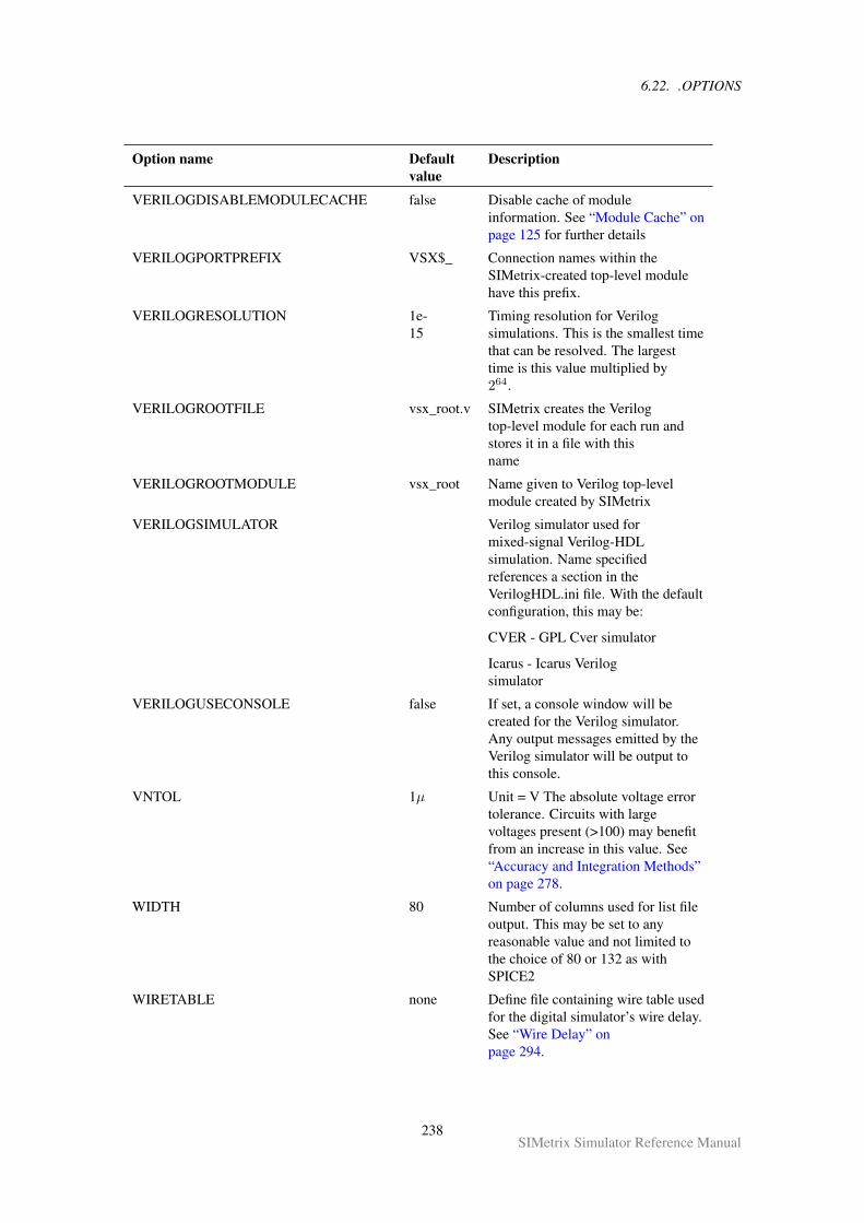
6.22. .OPTIONS
Option name Defaultvalue
Description
VERILOGDISABLEMODULECACHE false Disable cache of moduleinformation. See “Module Cache” onpage 125 for further details
VERILOGPORTPREFIX VSX$_ Connection names within theSIMetrix-created top-level modulehave this prefix.
VERILOGRESOLUTION 1e-15
Timing resolution for Verilogsimulations. This is the smallest timethat can be resolved. The largesttime is this value multiplied by264.
VERILOGROOTFILE vsx_root.v SIMetrix creates the Verilogtop-level module for each run andstores it in a file with thisname
VERILOGROOTMODULE vsx_root Name given to Verilog top-levelmodule created by SIMetrix
VERILOGSIMULATOR Verilog simulator used formixed-signal Verilog-HDLsimulation. Name specifiedreferences a section in theVerilogHDL.ini file. With the defaultconfiguration, this may be:
CVER - GPL Cver simulator
Icarus - Icarus Verilogsimulator
VERILOGUSECONSOLE false If set, a console window will becreated for the Verilog simulator.Any output messages emitted by theVerilog simulator will be output tothis console.
VNTOL 1µ Unit = V The absolute voltage errortolerance. Circuits with largevoltages present (>100) may benefitfrom an increase in this value. See“Accuracy and Integration Methods”on page 278.
WIDTH 80 Number of columns used for list fileoutput. This may be set to anyreasonable value and not limited tothe choice of 80 or 132 as withSPICE2
WIRETABLE none Define file containing wire table usedfor the digital simulator’s wire delay.See “Wire Delay” onpage 294.
238SIMetrix Simulator Reference Manual
6.23. .PARAM
6.23 .PARAM
.PARAM parameter_name [=] parameter_value [parameter_name [=] parameter_value]...
.PARAM parameter_name [=] AGAUSS(nominal, abs_variation, sigma, [multiplier]) ...
.PARAM parameter_name [=] AUNIF(nominal, abs_variation, [multiplier]) ...
.PARAM parameter_name [=] GAUSS(nominal, rel_variation, sigma, [multiplier]) ...
.PARAM parameter_name [=] UNIF(nominal, rel_variation, [multiplier]) ...
Defines a simulation variable for use in an expression. Expressions may be used to define deviceparameters, to define model parameters, for arbitrary sources and to define variables themselves. See“Using Expressions” on page 17 for details.
The syntax for the first form is described below. For details of the remaining forms (using AGAUSS,AUNIF, GAUSS and UNIF) see “Hspice Distribution Functions” on page 265.
parameter_name Sequence of alpha-numeric characters. Must begin with a letter orunderscore. May not contain spaces.
parameter_value Either:
A constant
OR
An expression enclosed by ‘’ and ‘’. See “Using Expressions” onpage 17.
6.23.1 Examples
.PARAM Vthresh = 2.4
.PARAM Vthresh = (Vhigh+Vlow)/2
.PARAM F0 1k Alpha 1 C1 2*c2
.PARAM R1 2/(2*pi*freq*C1*alpha
6.23.2 Netlist Order
.PARAM statements that resolve to a constant are order independent; they can be placed anywhere in anetlist. They can even be placed after another .PARAM expression that depends on its value (but note thisdoes not apply in subcircuits). .PARAM statements that are defined as an expression that depends on other.PARAMs also defined as an expression must be placed in sequential order. For example, the following isOK:
.PARAM C2 C1*alpha*alpha/4
.PARAM C1 1n
.PARAM alpha 1
.PARAM R1 2/(2*PI*F0*C2*alpha
The first .PARAM depends on alpha and C1 which are defined later in netlist. This is OK (as long as it isnot in a subcircuit) because icodealpha and C1 are constants. The fourth .PARAM depends on C2, whichis defined as an expression. The definition for must - and does in the above example - come before thedefinition of R1. The following would yield an error as the definition for C2 comes after the definition ofR1:
239SIMetrix Simulator Reference Manual
6.24. .POST_PROCESS
.PARAM R1 2/(2*PI*F0*C2*alpha
.PARAM C1 1n
.PARAM alpha 1
.PARAM C2 C1*alpha*alpha/4
Note that .PARAMs inside subcircuits are local to the subcircuit. This is explained in next section.
6.23.3 Subcircuit Parameters
Parameters may be declared within sub circuits. E.g
.subckt ADevice n1 n2 n3 n4
.PARAM Vthresh 3.5
...
...ends
In the above example, in reference to Vthresh within the subcircuit would use the value declared by the.PARAM declared inside the subcircuit. That value would not be available outside the subcircuitdefinition. Parameters may also be passed to subcircuits. E.g.
X1 1 2 3 4 ADevice : threshold=2.4
or
X1 1 2 3 4 ADevice params: threshold=2.4
Any reference to threshold within the subcircuit definition would use that value.
Default values for parameters may also be specified in subcircuit definition:
.subckt ADevice n1 n2 n3 n4 params: threshold=2.4
...
.ends
If that subcircuit is called without specifying threshold the default value of 2.4 will be used. Note that it isnot compulsory to declare default values.
6.23.4 Using .PARAM in Schematics
.PARAM statements may be appended to the netlist created by the schematic editor. For information onhow to do this, refer to “Adding Extra Netlist Lines” on page 2.
6.23.5 .PARAM in Libraries
.PARAM statements may be included in libraries specified using .LIB or by global definitions. SIMetrixwill search such libraries for any parameters used in expressions that are not found in the netlist.
6.24 .POST_PROCESS
.POST_PROCESS scriptname [arguments]
240SIMetrix Simulator Reference Manual
6.25. .PRINT
Invokes the SIMetrix script scriptname at the end of a successful simulation. If present arguments will bepassed to the script as a single string.
scriptname may the name of an embedded file defined using .FILE and .ENDF. For example, the followingwill cause the text “Simulation Complete” to be displayed in the command shell when the run is complete:
.FILE on_completeEcho "Simulation Complete".ENDF.POST_PROCESS on_complete
.POST_PROCESS may be used to perform measurements on simulation results for display in thecommand shell or written to a file.
.POST_PROCESS scripts will function even if the simulator is operating in a standalone mode in whichcase any displayed messages created from, for example, Echo or Show, will be directed to the simulator’soutput device. In console mode, this would be the console or terminal and in standalone GUI mode, thiswould be the message window in the simulator status box. As there is no environment available in thestandalone mode, not all script commands and functions will be available.
For information about the SIMetrix script language, please refer to the SIMetrix script reference manual.
6.25 .PRINT
.PRINT TRAN|AC|DC|NOISE|TF vector|expression ...
Instructs the simulator to output selected simulation data to the list file in tabulated form.
Where:
vector Name of vector to print. May be in SIMetrix native format or traditionalSPICE format (see notes below).
expression Arithmetic expression of vectors
6.25.1 Notes
A traditional SPICE2 command, this was not supported by SIMetrix until release 4.0. It is SPICE2compatible but also supports some additional features:
• NOISE and TF results may be output as well as TRAN, AC and DC
• You can put expressions as well as single values enclosed in ‘’ and ‘’. E.g.
.PRINT TRAN vout-q5_c
You can use the SPICE2 style method of accessing single voltages, differential voltages and devicecurrents. These are of the form:
Single ended voltage
funcname(nodename)
Differential voltage
funcname(nodename, nodename)
Device current
funcname(device_name)
241SIMetrix Simulator Reference Manual

6.25. .PRINT
Where:
242SIMetrix Simulator Reference Manual
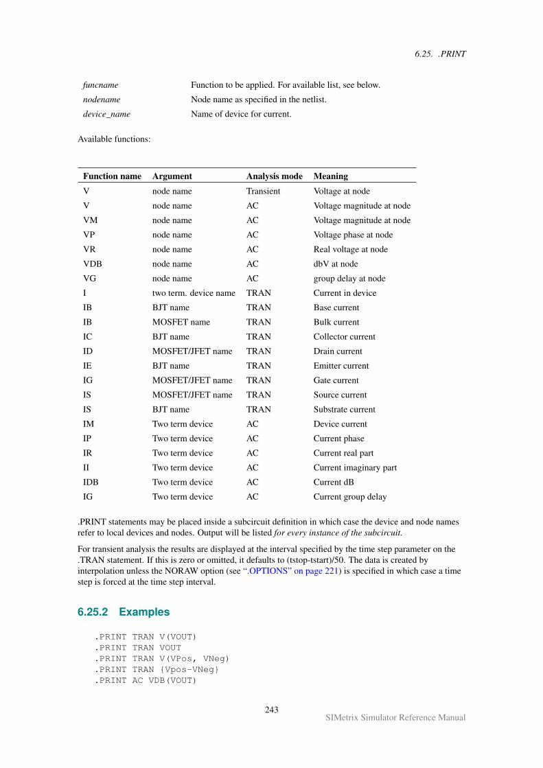
6.25. .PRINT
funcname Function to be applied. For available list, see below.
nodename Node name as specified in the netlist.
device_name Name of device for current.
Available functions:
Function name Argument Analysis mode Meaning
V node name Transient Voltage at node
V node name AC Voltage magnitude at node
VM node name AC Voltage magnitude at node
VP node name AC Voltage phase at node
VR node name AC Real voltage at node
VDB node name AC dbV at node
VG node name AC group delay at node
I two term. device name TRAN Current in device
IB BJT name TRAN Base current
IB MOSFET name TRAN Bulk current
IC BJT name TRAN Collector current
ID MOSFET/JFET name TRAN Drain current
IE BJT name TRAN Emitter current
IG MOSFET/JFET name TRAN Gate current
IS MOSFET/JFET name TRAN Source current
IS BJT name TRAN Substrate current
IM Two term device AC Device current
IP Two term device AC Current phase
IR Two term device AC Current real part
II Two term device AC Current imaginary part
IDB Two term device AC Current dB
IG Two term device AC Current group delay
.PRINT statements may be placed inside a subcircuit definition in which case the device and node namesrefer to local devices and nodes. Output will be listed for every instance of the subcircuit.
For transient analysis the results are displayed at the interval specified by the time step parameter on the.TRAN statement. If this is zero or omitted, it defaults to (tstop-tstart)/50. The data is created byinterpolation unless the NORAW option (see “.OPTIONS” on page 221) is specified in which case a timestep is forced at the time step interval.
6.25.2 Examples
.PRINT TRAN V(VOUT)
.PRINT TRAN VOUT
.PRINT TRAN V(VPos, VNeg)
.PRINT TRAN Vpos-VNeg
.PRINT AC VDB(VOUT)
243SIMetrix Simulator Reference Manual
6.26. .SENS
6.26 .SENS
.SENS V(nodename [,refnodename])| I(sourcename)
This statement instructs the simulator to perform a DC sensitivity analysis. In this analysis mode, a DCoperating point is first calculated then the linearised sensitivity of the specified circuit voltage or current toevery model and device parameter is evaluated. The results are output to the list file and they are alsoplaced in a new data group. The latter allows the data to be viewed in the message window (type Display)at the command line and can also be accessed from scripts for further analysis.
The number format used in the list file can be controlled by the SENSUSEEXPFORMAT option. Bydefault engineering format is used but this can be changed to exponential format with the setting:
.options SENSUSEEXPFORMAT
Instead of the results being written to the list file, they may alternatively be written to a text file using theSENSFILE option:
.options SENSFILE=<filename>
6.27 .SETSOA
.SETSOA [ LABEL=label ] [ MODEL=modelname | INST!=instname ] [DEVICE=device][!DERATING=derating] [MEAN] [ ALLOWUNUSED ] [ ALLOWWILD ]expr1=( min1, max1[, xwindow1] ) [ expr2=( min2, max2[, xwindow2] ) ... ]
Defines a Safe Operating Area (SOA) specification. If SOA testing is enabled the simulator will checksimulated results against this specification and record any violations. See .OPTIONS setting SOAMODEfor details on how to enable SOA tests.
The results of SOA testing are output to the list file by default and can optionally also be displayed in thecommand shell message window, or console window if run in non-GUI mode. They are also alwaysavailable via a script function GetSOAResults(). See .OPTIONS setting SOAOUTPUT for more details.
label Optional label that will be included in every violation report. You can usethe following symbolic values in this label:
%INST% - substituted with the instance name that violated thespecification. This is only meaningful if MODEL or INST are specified.(See below)
%MODEL% - substituted with the model name that violated thespecification. Only meaningful if MODEL is specified. (Seebelow)
%EXPR% - substituted with the expression that violated thespecification.
%SUBCKT% - applicable if the .SETSOA command is located within a.SUBCKT definition. Value is substituted with the subcircuit instancereference.
modelname If specified the expression or expressions supplied in expr1 etc. areapplied to every instance belonging to modelname. In this case theexpression may refer to node voltages and pin currents for each instanceprocessed. See details under expr1, expr2...
instname If specified the expression or expressions supplied in expr1 etc. areapplied to the specified instance (e.g. Q23, M10, R56). In this case theexpression may refer to node voltages and pin currents of the specifiedinstance. See details under expr1, expr2...
244SIMetrix Simulator Reference Manual
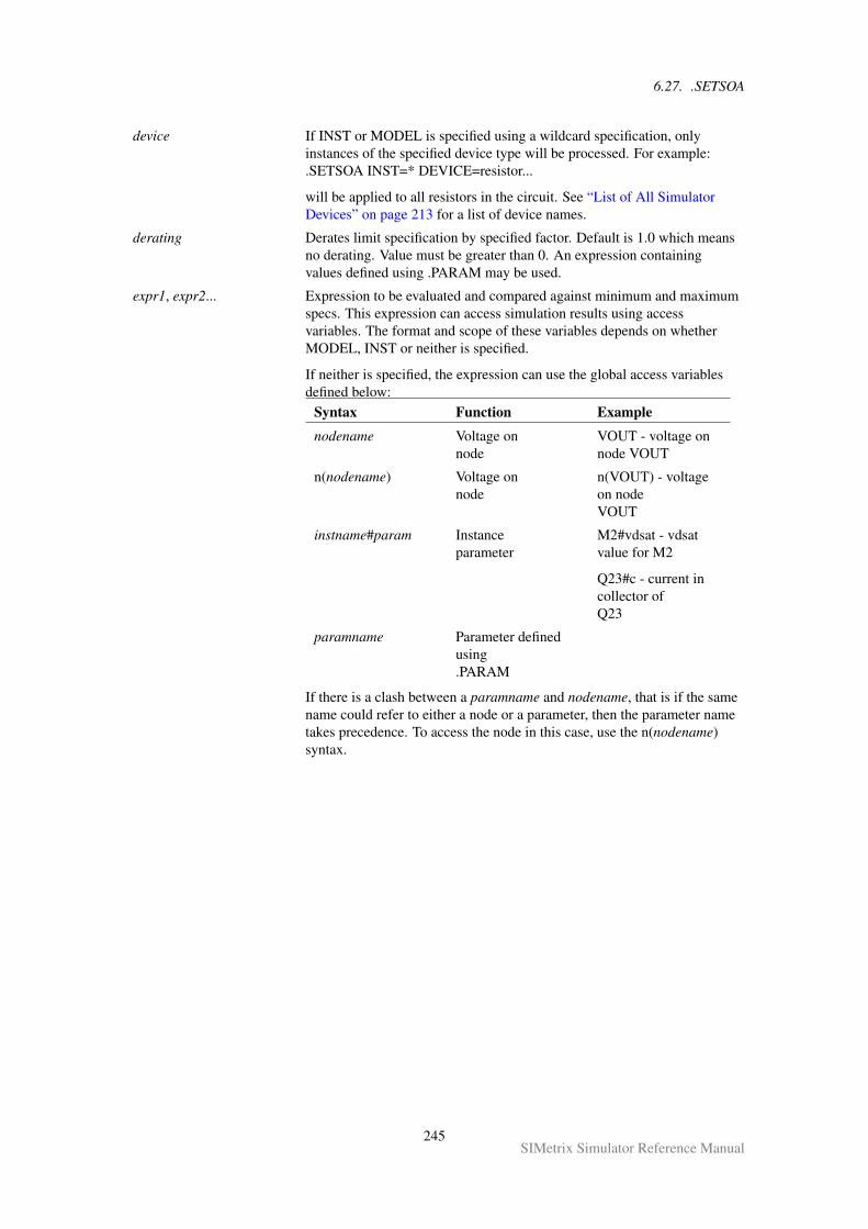
6.27. .SETSOA
device If INST or MODEL is specified using a wildcard specification, onlyinstances of the specified device type will be processed. For example:.SETSOA INST=* DEVICE=resistor...
will be applied to all resistors in the circuit. See “List of All SimulatorDevices” on page 213 for a list of device names.
derating Derates limit specification by specified factor. Default is 1.0 which meansno derating. Value must be greater than 0. An expression containingvalues defined using .PARAM may be used.
expr1, expr2... Expression to be evaluated and compared against minimum and maximumspecs. This expression can access simulation results using accessvariables. The format and scope of these variables depends on whetherMODEL, INST or neither is specified.
If neither is specified, the expression can use the global access variablesdefined below:
Syntax Function Example
nodename Voltage onnode
VOUT - voltage onnode VOUT
n(nodename) Voltage onnode
n(VOUT) - voltageon nodeVOUT
instname#param Instanceparameter
M2#vdsat - vdsatvalue for M2
Q23#c - current incollector ofQ23
paramname Parameter definedusing.PARAM
If there is a clash between a paramname and nodename, that is if the samename could refer to either a node or a parameter, then the parameter nametakes precedence. To access the node in this case, use the n(nodename)syntax.
245SIMetrix Simulator Reference Manual
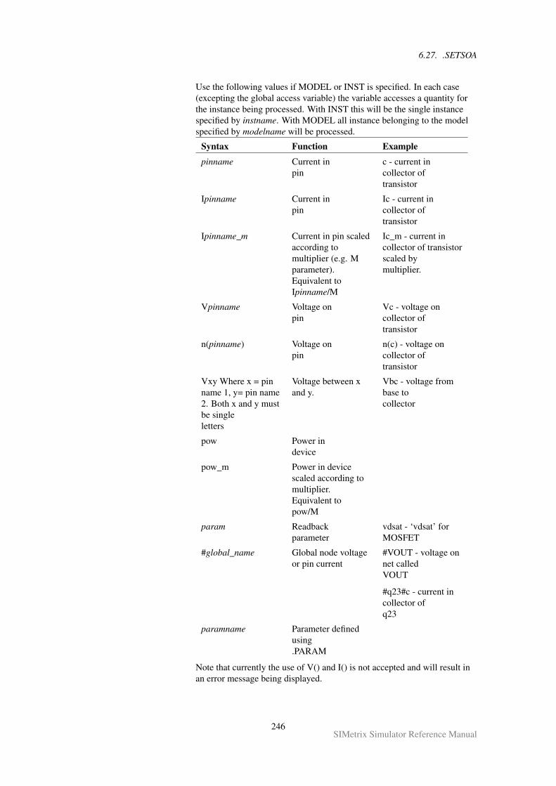
6.27. .SETSOA
Use the following values if MODEL or INST is specified. In each case(excepting the global access variable) the variable accesses a quantity forthe instance being processed. With INST this will be the single instancespecified by instname. With MODEL all instance belonging to the modelspecified by modelname will be processed.
Syntax Function Example
pinname Current inpin
c - current incollector oftransistor
Ipinname Current inpin
Ic - current incollector oftransistor
Ipinname_m Current in pin scaledaccording tomultiplier (e.g. Mparameter).Equivalent toIpinname/M
Ic_m - current incollector of transistorscaled bymultiplier.
Vpinname Voltage onpin
Vc - voltage oncollector oftransistor
n(pinname) Voltage onpin
n(c) - voltage oncollector oftransistor
Vxy Where x = pinname 1, y= pin name2. Both x and y mustbe singleletters
Voltage between xand y.
Vbc - voltage frombase tocollector
pow Power indevice
pow_m Power in devicescaled according tomultiplier.Equivalent topow/M
param Readbackparameter
vdsat - ‘vdsat’ forMOSFET
#global_name Global node voltageor pin current
#VOUT - voltage onnet calledVOUT
#q23#c - current incollector ofq23
paramname Parameter definedusing.PARAM
Note that currently the use of V() and I() is not accepted and will result inan error message being displayed.
246SIMetrix Simulator Reference Manual
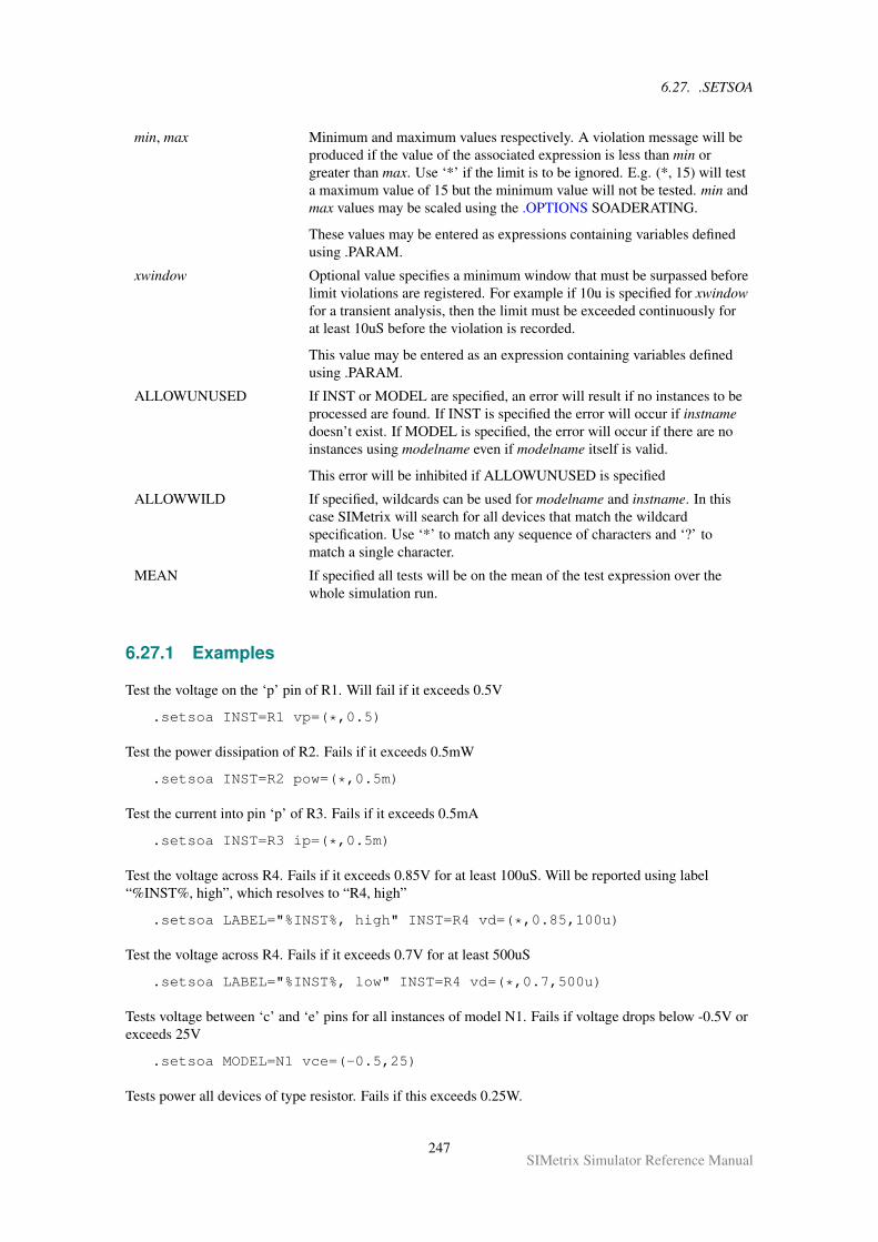
6.27. .SETSOA
min, max Minimum and maximum values respectively. A violation message will beproduced if the value of the associated expression is less than min orgreater than max. Use ‘*’ if the limit is to be ignored. E.g. (*, 15) will testa maximum value of 15 but the minimum value will not be tested. min andmax values may be scaled using the .OPTIONS SOADERATING.
These values may be entered as expressions containing variables definedusing .PARAM.
xwindow Optional value specifies a minimum window that must be surpassed beforelimit violations are registered. For example if 10u is specified for xwindowfor a transient analysis, then the limit must be exceeded continuously forat least 10uS before the violation is recorded.
This value may be entered as an expression containing variables definedusing .PARAM.
ALLOWUNUSED If INST or MODEL are specified, an error will result if no instances to beprocessed are found. If INST is specified the error will occur if instnamedoesn’t exist. If MODEL is specified, the error will occur if there are noinstances using modelname even if modelname itself is valid.
This error will be inhibited if ALLOWUNUSED is specified
ALLOWWILD If specified, wildcards can be used for modelname and instname. In thiscase SIMetrix will search for all devices that match the wildcardspecification. Use ‘*’ to match any sequence of characters and ‘?’ tomatch a single character.
MEAN If specified all tests will be on the mean of the test expression over thewhole simulation run.
6.27.1 Examples
Test the voltage on the ‘p’ pin of R1. Will fail if it exceeds 0.5V
.setsoa INST=R1 vp=(*,0.5)
Test the power dissipation of R2. Fails if it exceeds 0.5mW
.setsoa INST=R2 pow=(*,0.5m)
Test the current into pin ‘p’ of R3. Fails if it exceeds 0.5mA
.setsoa INST=R3 ip=(*,0.5m)
Test the voltage across R4. Fails if it exceeds 0.85V for at least 100uS. Will be reported using label“%INST%, high”, which resolves to “R4, high”
.setsoa LABEL="%INST%, high" INST=R4 vd=(*,0.85,100u)
Test the voltage across R4. Fails if it exceeds 0.7V for at least 500uS
.setsoa LABEL="%INST%, low" INST=R4 vd=(*,0.7,500u)
Tests voltage between ‘c’ and ‘e’ pins for all instances of model N1. Fails if voltage drops below -0.5V orexceeds 25V
.setsoa MODEL=N1 vce=(-0.5,25)
Tests power all devices of type resistor. Fails if this exceeds 0.25W.
247SIMetrix Simulator Reference Manual
6.28. .SUBCKT and .ENDS
.setsoa INST=* ALLOWWILD DEVICE=resistor pow=(*,0.25)
Tests the mean power in instance Q1. Fails if it exceeds “2*bjtderating”. “bjtderating” must be definedusing a .PARAM statement.
.setsoa LABEL="%INST%, pow(q1)" INST=Q1 MEAN pow=(*,2)derating=bjtderating
Calculates the expression “n(c)*(q1#c-d1#p)+n(b)*q1#b+n(e)*(q1#e+d1#p)” and fails if its mean exceeds1.0. Violations will be reported using label “%SUBCKT%, power”. Statement is intended to be placed in asubcircuit definition block and “%SUBCKT%” will resolve to the reference of the subcircuit call.
.setsoa LABEL="%SUBCKT%, power" MEAN "n(c)*(q1#cd1#p)+n(b)*q1#b+n(e)*(q1#e+d1#p)"=(*,1)
6.28 .SUBCKT and .ENDS
.SUBCKT subcktname n1 [ n2 ]...+ [ [params:] param_name1 [=] param_value1+ [param_name2 [=] param_value2]...]
This statement begins a subcircuit definition.
subcktname Subcircuit name. This must begin with aletter but may contain any legal ASCIIcharacter except any whitespace (space,tab) or ’ . ’ . The name must be unique i.e.no other subcircuits may have the samename.
n1, n2 etc. Node names available externally. Must notbe zero.
param_name, param_value Parameter name and value. This setsdefault values for parameters used withinthe subcircuit. These values can beoverridden for each subcircuit instance.See “Using Expressions” on page 17 formore info. Note that it is not compulsoryto declare default values for subcircuitparameters.
IMPORTANT: Either the params: specifier or the first ‘=’ may be omitted but not both. If both are omittedit becomes impossible for the netlist scanner to tell the difference between parameter names and nodenames.
.ENDS [ subcktname ]
Terminates a subcircuit definition. subcktname may be added for clarity but will be ignored by SIMetrix.
A subcircuit consists of a .subckt statement followed by a series of device or model descriptions andterminating in a .ends statement. A subcircuit is a circuit that can be called into the main circuit (or indeedanother subcircuit) by reference to its name. The .subckt statement is used to define the subcircuit while asubcircuit call - an ’X’ device - is used to create an instance of that subcircuit. Subcircuits have a numberof uses:
• To repeat a commonly used section of circuit.
248SIMetrix Simulator Reference Manual
6.30. .TF
• To hide detail from the main circuit to aid circuit readability.
• To distribute models of integrated devices such as op-amps.
For a detailed discussion see “Subcircuits” on page 29.
Subcircuit definitions usually reside in a text file and are read in as libraries. See User’s Manual for furtherdetails.
6.29 .TEMP
.TEMP temperature
This statement sets the default simulation temperature. Some devices can override this on a per instancebasis. Units are degrees centigrade.
6.30 .TF
.TF inner_sweep_spec [ V ] pos_out_node [ VN ] neg_out_node+ [[ INSRC ] in_source ] [ F frequency ] [RUNNAME=runname][SWEEP outer_sweep_spec ]
.TF inner_sweep_spec I source [ INSRC in_source ]+ [ F frequency ] [RUNNAME=runname] [SWEEP outer_sweep_spec ]
Spice Compatible:
.TF V( pos_out_node [, neg_out_node ]) in_source
.TF I (source) [ INSRC ] in_source
This statement instructs the simulator to perform a small signal transfer function analysis.
pos_out_node Output node.
neg_out_node Output reference node. Defaults to ground if omitted for standard SPICEsyntax.
in_source Name of input source to which input noise will be referred.
inner_sweep_spec See “General Sweep Specification” on page 190 for syntax. Defines sweepmode.
outer_sweep_spec If specified, analysis will be repeated according to this specification. See“General Sweep Specification” on page 190 for syntax.
frequency Frequency at which analysis will be performed for non-frequency sweeps.Default 0.
source Voltage source to specify output current.
runname If specified, the value for runname will be passed to the simulation datagroup as a string variable with name UserRunName. This may be used toidentify which analysis generated the data which is useful when runningnetlists with multiple analyses defined
249SIMetrix Simulator Reference Manual
6.31. .TRACE
6.30.1 Notes
The SIMetrix transfer function analysis remains syntax compatible with the SPICE version but issubstantially enhanced. The SPICE version performs the analysis at a single point with frequency = 0. TheSIMetrix implementation performs a swept analysis using the same sweep algorithm used for AC, DC andNOISE.
Transfer function analysis is similar to AC analysis in that it performs a swept small signal analysis.However, whereas AC analysis calculates the response at any circuit node from a (usually) single inputsource, transfer function analysis calculates the individual responses from each source in the circuit to asingle specified output node. This allows, for example, the series mode gain, common mode gain andpower supply rejection of an amplifier to be measured in one analysis. The same measurements could beperformed using AC analysis but several of them would need to be run. Transfer function mode alsocalculates output impedance or admittance and, if an input source is specified, input impedance.
The names of the output vectors will be of the form
Input voltage, output voltagesource_name#Vgain
Input voltage, output currentsource_name#Transconductance
Input current, output voltagesource_name#Transresistance
Input current, output currentsource_name#Igain
Output impedance for voltage out will be called Zout. For a current output, the output admittance will becalculated and will be named Yout.
If an input source is specified the input impedance will be calculated and called Zin.
Note that although the syntax for .TF retains compatibility with SPICE and earlier versions of SIMetrix,the output provided is slightly different. Firstly, the data is complex even if F=0 and secondly the names ofthe output vectors are different as detailed above.
6.30.2 Examples
SPICE compatible. Outputs results at DC.
.TF V(Vout) Vin
As above but decade sweep from 1k to 100k
.TF FREQ DEC 25 1K 100K V(Vout, 0) Vin
Note that in the above example the ‘0’ in V(Vout, 0) is compulsory. If is omitted, Vin will be assumed asthe reference node.
6.31 .TRACE
.TRACE vector_name [vector_name ...] graph_id
Set up a trace. This is graph plot that is updated as the simulation runs.
Where
250SIMetrix Simulator Reference Manual
6.32. .TRAN
vector_name is the name of a net or pin
graph_id is an integer between 1 and 999 to specify which graphs traces should use- see explanation below
graph_id is an arbitrary number that makes it possible to direct traces to different graphs. Two traces withthe same id will be always be put in the same graph. Traces from subsequent simulations with that id willalso go to that graph if it still exists otherwise a new one will be created. To force two traces to go toseparate graphs, use different id’s. Note that it doesn’t matter what the id’s value actually is - it could be 1or 100 - as long as traces that must go to the same graph use the same value.
Note that the AutoAxis feature available for normal plotting also works for Traces. So if a current andvoltage trace are both directed to the same graph, separate axes will be created for them.
6.31.1 Examples
.trace v1_p 1 q1#c 1
In the above example a voltage - v1_p - and a current - q1#c - will both be traced on the same graph. Asthey have different units, the AutoAxis feature will force the curves to two different y axes.
.trace v1_p 1 q1#c 2
In this example the voltage and current traces will be directed to different graph sheets.
6.31.2 Notes
The .TRACE statement has now been largely superseded by the .GRAPH statement (see “.GRAPH” onpage 199), which is much more flexible. However, the .TRACE statement is still useful for specifyingmultiple traces on a single line. .GRAPH can only specify one signal at a time.
6.32 .TRAN
.TRAN tstop
OR
.TRAN tstep tstop [ tstart [ tmaxstep ]] [ UIC ]+ [SNAPSTEP sstart sstop sstep]+ [SNAPSHOT slist]+ [SNAPMODE=DCOP|SAVESTATE|ALL]+ [FAST=fast_start] [RTNSTEP=rtnstep [RTNSTOP=rtnstop]+ [RTNSTART=rtnstart] ] [RUNNAME=runname]+ [SWEEP sweep_spec ]
This statement instructs the simulator to perform a transient analysis. In this mode the simulator computesthe behaviour of the circuit over the specified time interval. The circuit’s currents and voltages arecalculated at discrete time points separated by a variable time step. This time step is adjusted automaticallyby the simulator according to circuit activity. The circuit may contain any number of time varying voltageand current sources (stimuli) to simulate external signals, test generators etc.
251SIMetrix Simulator Reference Manual
6.32. .TRAN
tstep This defines the interval for tabulated results specified by the .PRINTstatement. It also defines the output interval for all data if the NORAWoption is specified. If there are no .PRINT statements in the netlist andNORAW is not being used, this can be set to zero or omitted altogether asin form 1 above. If set to zero it defaults to (tstop-tstart)/50.
tstep is also used to define default values for pulse and exponentialstimuli.
Note that if tstep and NORAW are specified a time point is forced at tstepintervals to calculate the output. This differs from other SPICE programswhich generate output at tstep by interpolation.
tstep does not control the time step used by the simulator. This iscontrolled automatically according to circuit activity.
tstop Stop time. Note that if running in GUI mode, a transient analysis can berestarted from the front end. See User’s Manual/Analysis Modes/TransientAnalysis/restarting a Transient Run for details.
tstart Start time. This is the time at which the storage of transient analysisoutputs commences. It is not the time at which the analysis begins; this isalways zero. tstart is zero if it is omitted.
tmaxstep Maximum time step. The simulator uses the largest time step possible toachieve the required accuracy but will not increase it beyond this value. Ifnot specified it is set to (tstop-tstart)/50.
UIC If specified a DC operating point is not calculated and initial conditionspecifications are used instead
fast_start If specified, the simulation will run at reduced accuracy but higher speedfor the time specified by this parameter. The reduced accuracy isimplemented by altering a number of tolerances and internal parameters.See notes below for more details.
rtnstep If this parameter is specified, Real Time Noise analysis will be enabled.Note that this feature is not available with all versions of the program.rtnstep specifies the step size of the noise generators. See “Real TimeNoise Analysis” on page 253.
rtnstart Specifies time at which real time noise generators are switched on.
rtnstop Specifies time at which real time noise generators are switched off.
sstart Time at which snapshot saving begins. See below for information onsnapshots.
sstop Time at which snapshot saving stops. See below for information onsnapshots
sstep Interval between snapshot points. See below for information onsnapshots
slist One or more values defining absolute times at which snap shots are saved.See below for information on snapshots
runname If specified, the value for runname will be passed to the simulation datagroup as a string variable with name UserRunName. This may be used toidentify which analysis generated the data which is useful when runningnetlists with multiple analyses defined
252SIMetrix Simulator Reference Manual
6.33. Real Time Noise Analysis
DCOP, SAVESTATE,ALL
Snapshot mode.
DCOP: Saves bias point information only.
SAVESTATE: Saves state of circuit for subsequent reload for small signalanalysis
ALL: Both of the above
The default is DCOP.
6.32.1 Fast Start
If the FAST parameter is specified, the simulation will begin with a number of tolerances and internalparameters altered to speed up the simulation at the expense of accuracy. Just before the end of the faststart period, these tolerances and parameters will be gradually restored to their normal values. Fast start isan aid for simulating circuits such as switching power supplies and oscillators for which the initial start upperiod is not of interest but takes a long simulation time. Note that although the fast start interval can runsometimes as much as twice as quickly as normal, the fact that accuracy is impaired can mean that the finalsteady state reached may not be very accurate. This means that after the fast start period, an additionalsettling time may be required for full accuracy to be reached.
Fast start sets the values of POINTTOL and RELTOL according to the value specified byFASTPOINTTOL and FASTRELTOL respectively.
6.32.2 Snapshots
This feature allows the state of a simulation to be saved at user specified times during a transient analysis.The states saved can subsequently be reloaded to perform small signal AC analyses.
This allows the small signal response of a circuit to be examined at any point during a transient analysis.This is especially useful in situations where a circuit is found to be unstable in a transient run but thisinstability cannot be reproduced at the operating point usually derived for an AC analysis.
The bias point information at the snapshot time may also optionally be saved. This information is output tothe list file.
To specify snapshot output, specify either the SNAPSHOT or SNAPSTEP keywords with their associatedparameters.
To initialise a small signal analysis with snapshot data, you must specify the SNAPSHOT step mode of amulti-step analysis. See “Multi Step Analyses” on page 192 for details.
6.33 Real Time Noise Analysis
This is an extension of transient analysis rather than a separate analysis mode. When activated, real timenoise sources are added to all noisy devices with a magnitude and frequency distribution calculated usingthe same equations used for small signal analysis. This allows noise analysis to be performed on sampleddata systems and oscillators.
To use real time noise analysis, the following parameters may be added to the .TRAN analysis line.
RTNstep Source step size in seconds. This will need to be small enough to cover thefrequency range of interest. The noise magnitude starts rolling off at about1/3*stepsize. Default=0 i.e. real time noise analysis disabled.
RTNstart Optional. Time after analysis start at which the noise sources will beenabled. Default = zero
253SIMetrix Simulator Reference Manual

6.33. Real Time Noise Analysis
RTNstop Optional. Time after analysis start at which the noise sources will bedisabled. Default = stop time.
The parameters added to the .TRAN line must be named in the same way as .MODEL parameters arenamed.
6.33.1 Example
.TRAN 0 1m RTNstep=1u RTNstart=500u
Analysis time 1m, RTN step size 1u, real time sources start at 500u. The step size parameter - i.e. the firstparameter on the .TRAN line - must be supplied if real time noise parameters are to be included. This isonly to comply with the syntax rules not because the step size is needed for any other purpose. In mostcases, just set it to zero as in the above example.
6.33.2 Test Results
To test real time noise and verify it’s accuracy we ran a test on a number of circuits which compare ACnoise with real time noise. The procedure was to run real time noise analysis 50 times then plot theaveraged Fourier spectrum. This test was repeated for different transient run times and step sizes to build anoise spectrum over several decades. The graph below is the result of one such test. This was carried outon the BSIM3 buffer circuit provided in one of the examples except that a value for AF - the flicker noiseparameter - was added to the models. As can be seen in the graph below the real time noise results stronglyfollow the AC noise results.
Similar tests were performed on circuits containing each of the major noise generating devices includingdiodes, BJTs, JFETs, resistors (including its flicker noise parameter) and also the NXP MOS9 andMEXTRAM devices. All showed results similar to below with a close similarity between AC noise andreal time noise.
These tests were performed using a simple script. This script is called rtntest.sxscr and can be found on theinstallation CDROM at SCRIPTS/EXAMPLES. This can also be found at our web site. Please refer to“Further Documentation” on page 38 for details.
254SIMetrix Simulator Reference Manual
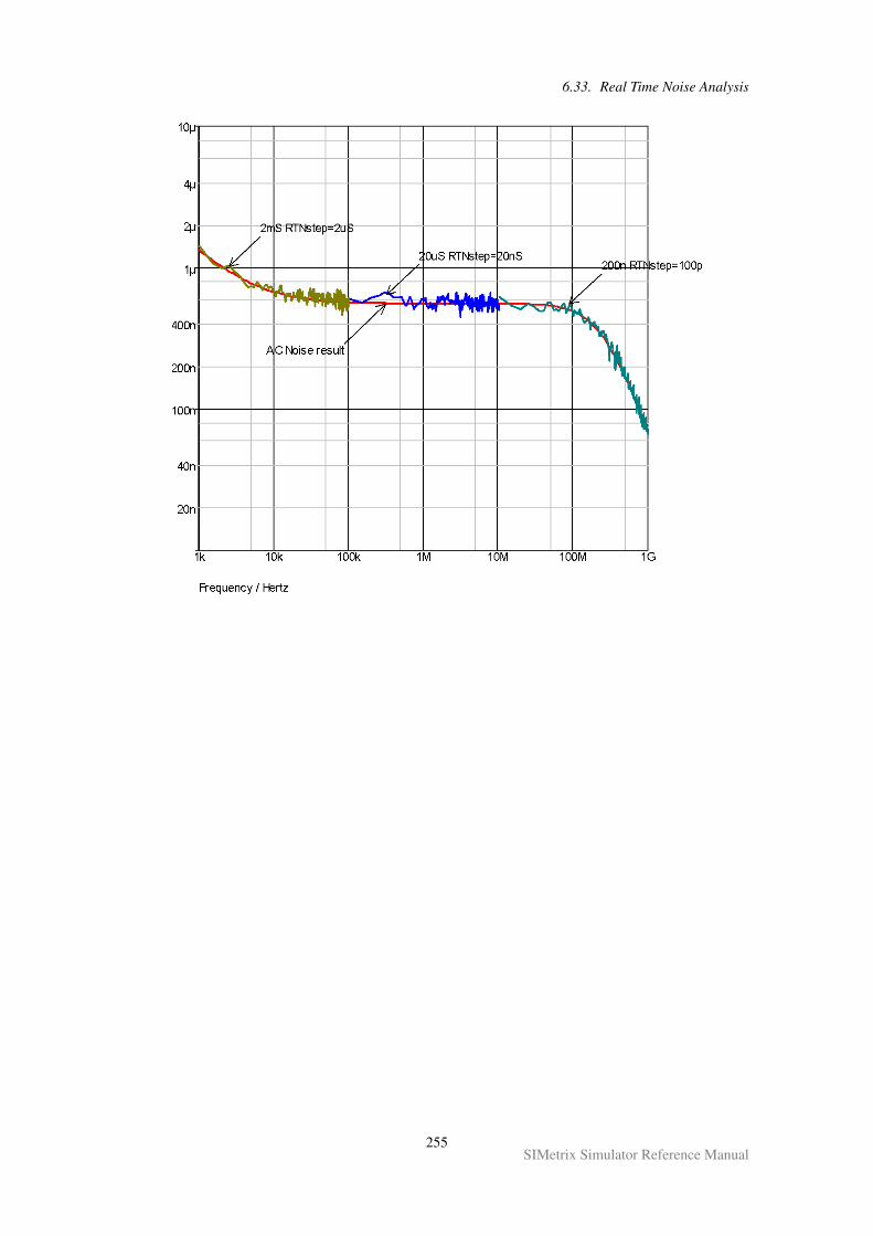
6.33. Real Time Noise Analysis
255SIMetrix Simulator Reference Manual
Chapter 7
Monte Carlo Analysis
7.1 Overview
Monte Carlo analysis is a procedure to assess manufacturing yields by repeating simulation runs withvarying applied random variations to component parameters. The technique is very powerful and usuallygives a more realistic result than worst-case analysis which varies component values to their extremes in amanner which produces the worst possible result.
The implementation of Monte Carlo analysis in SIMetrix has been designed to be quick to set up forsimple cases while still providing the required flexibility for more advanced requirements as might berequired for integrated circuit design.
SIMetrix offers a level of flexibility for tolerance specification that cannot be found in other productsincluding some high priced UNIX based applications. It is possible, for example, for different modelparameters to be dependent on a single random variable. This makes it possible to model the fact that anumber of model parameters might be dependent on a single physical characteristic, for example, the basewidth of a bipolar transistor. Of course, lot tolerances are also implemented accounting for the matching ofdevices in integrated circuits and other multiple components built onto a common substrate. However, inmany products, lot tolerances can only be applied to the same type of device. In SIMetrix it is possible tomodel parametric relationships between different types of device which occur in integrated circuits butwhich are rarely taken into account.
As well as conventional multiple step Monte Carlo analysis, single step Monte Carlo sweeps may also beperformed. These are available for the four swept modes, .AC, .DC, .NOISE and .TF. For example, aMonte Carlo analysis of the DC offset voltage of an amplifier can be performed using a single run of .DCusing a special sweep mode. This is dramatically faster than the alternative of repeated .OP runs. This typeof analysis can also be used to analyse the gain of an amplifier at a single frequency using .AC or .TF oreven the noise, again at a single frequency, using .NOISE.
7.2 Specifying a Monte Carlo Run
Monte Carlo runs are invoked in the same way as multi-step analyses (see “General Sweep Specification”on page 190). The basic syntax is:
.analysis_name analysis_parameters SWEEP MONTE num_runs NUMCORES=num_cores
Where:
.analysis_name Dot statement for analysis. Either .TRAN, .AC, .DC, .NOISE, .TF
analysis_parameters Specific parameters for that analysis
256SIMetrix Simulator Reference Manual
7.3. Specifying a Single Step Monte Carlo Sweep
num_runs Number of runs
num_cores Specify the number of processor cores to use.
7.2.1 Examples
Run 10 Monte Carlo runs for 1mS transient analysis
.TRAN 1m SWEEP MONTE 10
Run 1000 Monte Carlo steps for 1mS transient analysis using 4 processor cores. This will split the 1000steps into 4 cores with each running 250 steps
.TRAN 1m SWEEP MONTE 1000 NUMCORES=4
100 Runs of a DC Sweep
.DC V1 0 5 0.01 SWEEP MONTE 100
AC sweep of voltage source V5 from -300mV to 300mV. Repeat 50 times
.AC DEVICE=V5 LIN 100 -300m 300m F=100000 SWEEP MONTE 50
7.3 Specifying a Single Step Monte Carlo Sweep
Monte Carlo sweep is one of the six modes available to the swept analysis modes, .AC, .DC .NOISE and.TF. The other modes are explained in “General Sweep Specification” on page 190. The general syntax is:
.analysis_name MONTE num_points analysis_parameters
Where:
.analysis_name Dot statement for analysis. Either .AC, .DC, .NOISE, .TF
analysis_parameters Specific parameters for that analysis
num_points Number of points in sweep
7.3.1 Examples
1000 point Monte Carlo sweep.
.DC MONTE 1000
AC Monte Carlo sweep 100 steps. Frequency = 10K. This is useful if - say - you are interested in the gainof an amplifier at one frequency and it needs to lie within a defined tolerance. Previously you would needto repeat an AC sweep at a single frequency to achieve this which could take a long time especially if thecircuit has a difficult to find operating point. The analysis defined by the following line will take very littletime even for a large circuit.
.AC MONTE 100 F=10K
257SIMetrix Simulator Reference Manual
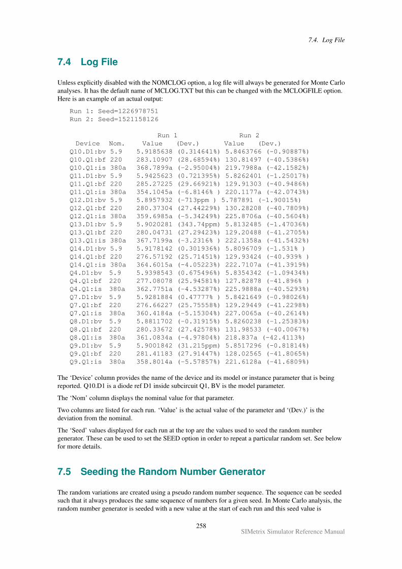
7.4. Log File
7.4 Log File
Unless explicitly disabled with the NOMCLOG option, a log file will always be generated for Monte Carloanalyses. It has the default name of MCLOG.TXT but this can be changed with the MCLOGFILE option.Here is an example of an actual output:
Run 1: Seed=1226978751Run 2: Seed=1521158126
Run 1 Run 2Device Nom. Value (Dev.) Value (Dev.)
Q10.D1:bv 5.9 5.9185638 (0.314641%) 5.8463766 (-0.90887%)Q10.Q1:bf 220 283.10907 (28.68594%) 130.81497 (-40.5386%)Q10.Q1:is 380a 368.7899a (-2.95004%) 219.7988a (-42.1582%)Q11.D1:bv 5.9 5.9425623 (0.721395%) 5.8262401 (-1.25017%)Q11.Q1:bf 220 285.27225 (29.66921%) 129.91303 (-40.9486%)Q11.Q1:is 380a 354.1045a (-6.8146% ) 220.1177a (-42.0743%)Q12.D1:bv 5.9 5.8957932 (-713ppm ) 5.787891 (-1.90015%)Q12.Q1:bf 220 280.37304 (27.44229%) 130.28208 (-40.7809%)Q12.Q1:is 380a 359.6985a (-5.34249%) 225.8706a (-40.5604%)Q13.D1:bv 5.9 5.9020281 (343.74ppm) 5.8132485 (-1.47036%)Q13.Q1:bf 220 280.04731 (27.29423%) 129.20488 (-41.2705%)Q13.Q1:is 380a 367.7199a (-3.2316% ) 222.1358a (-41.5432%)Q14.D1:bv 5.9 5.9178142 (0.301936%) 5.8096709 (-1.531% )Q14.Q1:bf 220 276.57192 (25.71451%) 129.93424 (-40.939% )Q14.Q1:is 380a 364.6015a (-4.05223%) 222.7107a (-41.3919%)Q4.D1:bv 5.9 5.9398543 (0.675496%) 5.8354342 (-1.09434%)Q4.Q1:bf 220 277.08078 (25.94581%) 127.82878 (-41.896% )Q4.Q1:is 380a 362.7751a (-4.53287%) 225.9888a (-40.5293%)Q7.D1:bv 5.9 5.9281884 (0.47777% ) 5.8421649 (-0.98026%)Q7.Q1:bf 220 276.66227 (25.75558%) 129.29449 (-41.2298%)Q7.Q1:is 380a 360.4184a (-5.15304%) 227.0065a (-40.2614%)Q8.D1:bv 5.9 5.8811702 (-0.31915%) 5.8260238 (-1.25383%)Q8.Q1:bf 220 280.33672 (27.42578%) 131.98533 (-40.0067%)Q8.Q1:is 380a 361.0834a (-4.97804%) 218.837a (-42.4113%)Q9.D1:bv 5.9 5.9001842 (31.215ppm) 5.8517296 (-0.81814%)Q9.Q1:bf 220 281.41183 (27.91447%) 128.02565 (-41.8065%)Q9.Q1:is 380a 358.8014a (-5.57857%) 221.6128a (-41.6809%)
The ‘Device’ column provides the name of the device and its model or instance parameter that is beingreported. Q10.D1 is a diode ref D1 inside subcircuit Q1, BV is the model parameter.
The ‘Nom’ column displays the nominal value for that parameter.
Two columns are listed for each run. ‘Value’ is the actual value of the parameter and ‘(Dev.)’ is thedeviation from the nominal.
The ‘Seed’ values displayed for each run at the top are the values used to seed the random numbergenerator. These can be used to set the SEED option in order to repeat a particular random set. See belowfor more details.
7.5 Seeding the Random Number Generator
The random variations are created using a pseudo random number sequence. The sequence can be seededsuch that it always produces the same sequence of numbers for a given seed. In Monte Carlo analysis, therandom number generator is seeded with a new value at the start of each run and this seed value is
258SIMetrix Simulator Reference Manual
7.6. Specifying Tolerances
displayed in the log file (see above). It is also possible to fix the first seed that is used using the SEEDoption. This makes it possible to repeat a run. To do this, note the seed value of the run of interest then addthe line:
.OPTIONS SEED=seed_value
For example if you wanted to repeat run 2 in the above example you would add this line:
.OPTIONS SEED=1521158126
The first run of each Monte Carlo analysis will use the same random values as run 2 above. Note thisassumes that only changes in values are made to the circuit. Any topology change will upset the sequence.
7.6 Specifying Tolerances
7.6.1 Overview
Tolerances for Monte Carlo analysis may be specified by one of the following methods:
1. Using a distribution function in an expression.
2. Using the device parameters TOL, MATCH and LOT
Method 1 above is the most general and flexible. TOL, MATCH and LOT parameters are providedprimarily for backward compatibility but may also be more convenient in some circumstances.
7.6.2 Distribution Functions
To specify Monte Carlo tolerance for a model or device parameter, define the parameter using anexpression (see “Using Expressions” on page 17) containing one of the following functions:
Name Distribution Lot?
GAUSS(tol) Gaussian (3-sigma) No
GAUSSL(tol) Gaussian (3-sigma) Yes
UNIF(tol) Uniform No
UNIFL(tol) Uniform Yes
UNIF2(tolupper, tollower) Uniform No
UNIFL2(tolupper, tollower) Uniform Yes
WC(tol) Worst case No
WCL(tol) Worst case Yes
WC2(tolupper, tollower) Worst case No
WCL2(tolupper, tollower) Worst case Yes
GAUSSTRUNC(tol, sigma) Truncated Gaussian No
GAUSSTRUNCL(tol, sigma) Truncated Gaussian Yes
DISTRIBUTION(args) User defined distribution No
DISTRIBUTIONL(args) User defined distribution Yes
UD(args) User defined distribution (alias) No
UDL(args) User defined distribution (alias) Yes
259SIMetrix Simulator Reference Manual
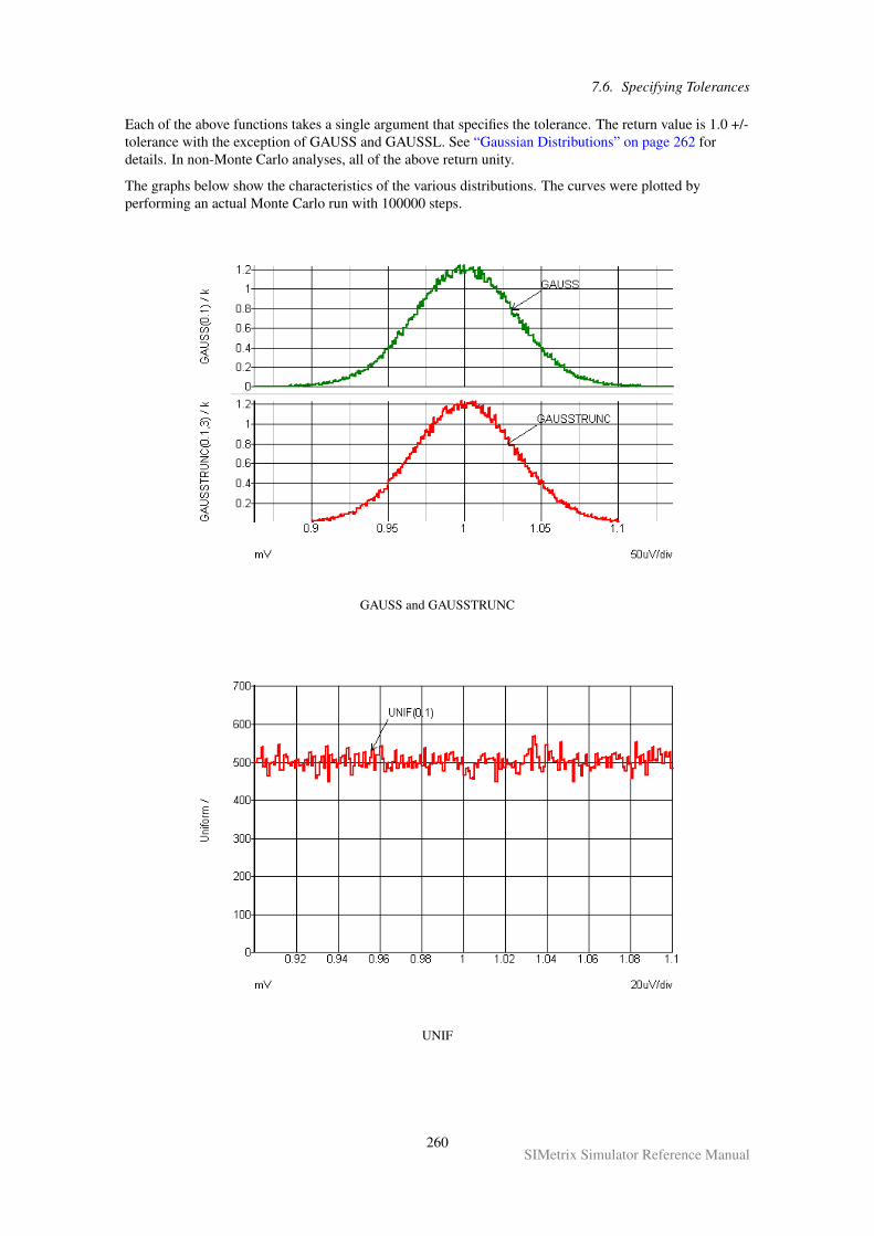
7.6. Specifying Tolerances
Each of the above functions takes a single argument that specifies the tolerance. The return value is 1.0 +/-tolerance with the exception of GAUSS and GAUSSL. See “Gaussian Distributions” on page 262 fordetails. In non-Monte Carlo analyses, all of the above return unity.
The graphs below show the characteristics of the various distributions. The curves were plotted byperforming an actual Monte Carlo run with 100000 steps.
GAUSS and GAUSSTRUNC
UNIF
260SIMetrix Simulator Reference Manual
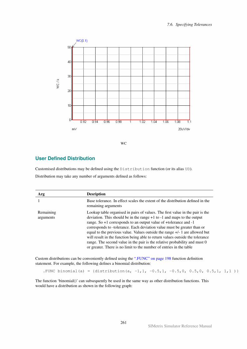
7.6. Specifying Tolerances
WC
User Defined Distribution
Customised distributions may be defined using the Distribution function (or its alias UD).
Distribution may take any number of arguments defined as follows:
Arg Desription
1 Base tolerance. In effect scales the extent of the distribution defined in theremaining arguments
Remainingarguments
Lookup table organised in pairs of values. The first value in the pair is thedeviation. This should be in the range +1 to -1 and maps to the outputrange. So +1 corresponds to an output value of +tolerance and -1corresponds to -tolerance. Each deviation value must be greater than orequal to the previous value. Values outside the range +/- 1 are allowed butwill result in the function being able to return values outside the tolerancerange. The second value in the pair is the relative probability and must 0or greater. There is no limit to the number of entries in the table
Custom distributions can be conveniently defined using the “.FUNC” on page 198 function definitionstatement. For example, the following defines a binomial distribution:
.FUNC binomial(a) = distribution(a, -1,1, -0.5,1, -0.5,0, 0.5,0, 0.5,1, 1,1 )
The function ‘binomial()’ can subsequently be used in the same way as other distribution functions. Thiswould have a distribution as shown in the following graph:
261SIMetrix Simulator Reference Manual
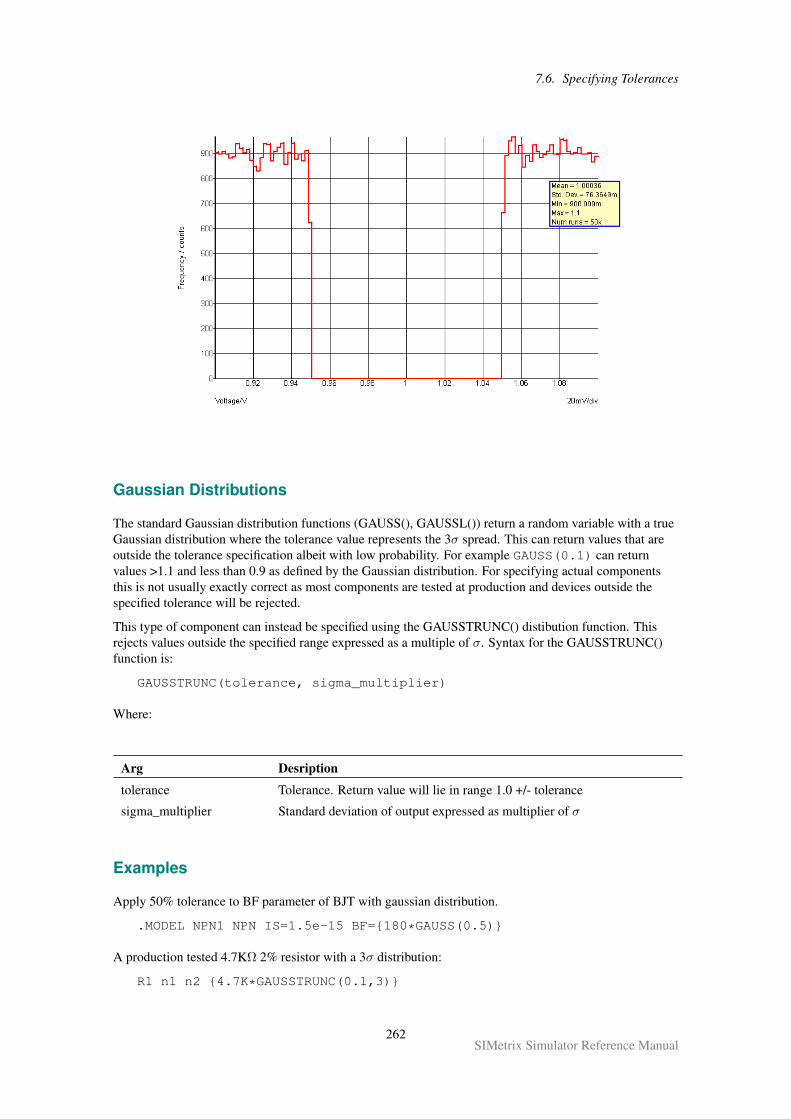
7.6. Specifying Tolerances
Gaussian Distributions
The standard Gaussian distribution functions (GAUSS(), GAUSSL()) return a random variable with a trueGaussian distribution where the tolerance value represents the 3σ spread. This can return values that areoutside the tolerance specification albeit with low probability. For example GAUSS(0.1) can returnvalues >1.1 and less than 0.9 as defined by the Gaussian distribution. For specifying actual componentsthis is not usually exactly correct as most components are tested at production and devices outside thespecified tolerance will be rejected.
This type of component can instead be specified using the GAUSSTRUNC() distibution function. Thisrejects values outside the specified range expressed as a multiple of σ. Syntax for the GAUSSTRUNC()function is:
GAUSSTRUNC(tolerance, sigma_multiplier)
Where:
Arg Desription
tolerance Tolerance. Return value will lie in range 1.0 +/- tolerance
sigma_multiplier Standard deviation of output expressed as multiplier of σ
Examples
Apply 50% tolerance to BF parameter of BJT with gaussian distribution.
.MODEL NPN1 NPN IS=1.5e-15 BF=180*GAUSS(0.5)
A production tested 4.7KΩ 2% resistor with a 3σ distribution:
R1 n1 n2 4.7K*GAUSSTRUNC(0.1,3)
262SIMetrix Simulator Reference Manual
7.6. Specifying Tolerances
Lot Tolerances
The lot versions of the functions specify a distribution to be applied to devices whose tolerances track.These functions will return the same random value for all devices that reference the same model.
Note that the same effect as LOT tolerances can be achieved using random variables and subcircuits. Fordetails see “Creating Random Variables” on page 264
Lot Tolerance Examples
Specify 50% uniform lot tolerance and 5% gaussian device tolerance for BF parameter
.MODEL NPN1 NPN IS=1.5E-15 BF=180*GAUSS(0.05)*UNIFL(0.5)
Here is an abbreviated log file for a run of a circuit using 2 devices referring to the above model:
Run 1 Run 2Device Nom. Value (Dev.) Value (Dev.)Q1:bf 180 93.308486 (-48.162% ) 241.3287 (34.0715% )Q2:bf 180 91.173893 (-49.3478%) 245.09026 (36.16126%)
Run 3 Run 4Device Nom. Value (Dev.) Value (Dev.)Q1:bf 180 185.95824 (3.310133%) 210.46439 (16.92466%)Q2:bf 180 190.8509 (6.02828% ) 207.04202 (15.02335%)
For the four runs BF varies from 91 to 245 but the two devices never deviate from each other by more thanabout 2.7%.
Notes
The tracking behaviour may not be as expected if the model definition resides within a subcircuit. When amodel is defined in a subcircuit, a copy of that model is created for each device that calls the subcircuit.Here is an example:
XQ100 VCC INN Q100_E 0 NPN1XQ101 VCC INP Q101_E 0 NPN1
.SUBCKT NPN1 1 2 3 SUBQ1 1 2 3 SUB N1Q2 SUB 1 2 SUB P1
.MODEL N1 NPN IS=1.5E-15 BF=180*GAUSS(0.05)*UNIFL(0.5)
.ENDS
In the above, XQ100 and XQ101 will not track. Two devices referring to N1 inside the subcircuitdefinition would track each other but different instances of the subcircuit will not. To make XQ100 andXQ101 track, the definition of N1 should be placed outside the subcircuit. E.g.
XQ100 VCC INN Q100_E 0 NPN1XQ101 VCC INP Q101_E 0 NPN1
.SUBCKT NPN1 1 2 3 SUBQ1 1 2 3 SUB N1Q2 SUB 1 2 SUB P1
.ENDS
.MODEL N1 NPN IS=1.5E-15 BF=180*GAUSS(0.05)*UNIFL(0.5)
263SIMetrix Simulator Reference Manual
7.6. Specifying Tolerances
Creating Random Variables
It is possible to place distribution functions in .PARAM expressions to create a random variable. Thisprovides a means of describing a relationship between different devices or different parameters within thesame device.
Random variables may be created at the top level in which case they will be global and have the samevalue wherever they are used. Random variables may also be created inside subcircuit definitions. In thiscase they are local to the subcircuit and will have the same value for all devices and parameters within thesubcircuit but a different value for different instances of the subcircuit.
Example 1 In this example we make a BJT model using a subcircuit. The random variable is createdinside the subcircuit so will have the same value for parameters defined in the subcircuit but will havedifferent values for multiple instances
.subckt NPN1 c b e
.PARAM rv1 = UNIF(0.5)Q1 c b e NPN1.MODEL NPN1 NPN BF=rv1*180 TF=1e-11*rv1.ends
For all devices using that model, BF and TF will always have a fixed relationship to each other eventhough each parameter can vary by +/-50% from one device to the next.
Here is the log of a run carried out on a circuit with two of the above devices:
Run 1 Run 2Run 1: Seed=1651893287
Run 1Device Nom. Value (Dev.)Q1.Q1:bf 180 148.83033746 (-17.3164792%)Q1.Q1:tf 10p 8.268352081p (-17.3164792%)Q2.Q1:bf 180 129.69395145 (-27.9478048%)Q2.Q1:tf 10p 7.205219525p (-27.9478048%)
Run 2: Seed=763313972
Run 2Device Nom. Value (Dev.)Q1.Q1:bf 180 265.86053442 (47.7002969% )Q1.Q1:tf 10p 14.77002969p (47.7002969% )Q2.Q1:bf 180 186.41647487 (3.564708261%)Q2.Q1:tf 10p 10.35647083p (3.564708261%)
Notice that the BF and TF parameters always deviate by exactly the same amount for each device.However, the two devices do not track each other. If this were needed we would define the randomvariable outside the subcircuit at the netlist’s top level:
.PARAM rv1 = UNIF(0.5)
.subckt NPN1 c b eQ1 c b e NPN1.MODEL NPN1 NPN BF=rv1*180 TF=1e-11*rv1.ends
Here is the log for the above:
Run 1: Seed=1608521901
Run 1
264SIMetrix Simulator Reference Manual
7.6. Specifying Tolerances
Device Nom. Value (Dev.)Q1.Q1:bf 180 249.54358268 (38.63532371%)Q1.Q1:tf 10p 13.86353237p (38.63532371%)Q2.Q1:bf 180 249.54358268 (38.63532371%)Q2.Q1:tf 10p 13.86353237p (38.63532371%)
Run 2: Seed=80260241
Run 2Device Nom. Value (Dev.)Q1.Q1:bf 180 116.33087232 (-35.3717376%)Q1.Q1:tf 10p 6.46282624p (-35.3717376%)Q2.Q1:bf 180 116.33087232 (-35.3717376%)Q2.Q1:tf 10p 6.46282624p (-35.3717376%)
7.6.3 Hspice Distribution Functions
SIMetrix supports the Hspice method of defining Monte Carlo tolerances. This feature needs to be enabledwith an option setting; see “Enabling Hspice Distribution Functions” on page 266. The Hspice methoduses random variables created using a special .PARAM syntax in one of the following form:
.PARAM parameter_name [=] AGAUSS(nominal, abs_variation, sigma, [multiplier]) ...
.PARAM parameter_name [=] AUNIF(nominal, abs_variation, [multiplier]) ...
.PARAM parameter_name [=] GAUSS(nominal, rel_variation, sigma, [multiplier]) ...
.PARAM parameter_name [=] UNIF(nominal, rel_variation, [multiplier]) ...
Where:
parameter_name Name of random variable
nominal Nominal value
abs_variation Absolute variation. AGAUSS and AUNIF vary the nominal value +/- thisvalue
rel_variation Relative variation. GAUSS and UNIF vary the nominal value by +/-rel_variation*nominal
sigma Scales abs_variation and rel_variation for functions GAUSS andAGAUSS. E.g. if sigma is 3 the standard deviation of the result is dividedby 3. So AGAUSS(0,0.01,3) would yield a +/-1% tolerance with a 3 sigmadistribution
multiplier If included this must be set to 1 otherwise an error message will bedisplayed and the simulation aborted. Included for compatibility withexisting model files only.
Random variables created using the above method do not behave in the same way as regular parameterscreated using the native SIMetrix distribution functions. They actually behave like function calls andreturn a different value each time they are used. Random variables created using .param and a nativedistribution function are evaluated just once and always return the same value. Internally, the above areimplemented using a .FUNC definition to define a function with no arguments.
For example, the following are both quite legal:
.PARAM rv1 = UNIF(10,1)
265SIMetrix Simulator Reference Manual
7.6. Specifying Tolerances
.PARAM rv2 = 'UNIF(10,1)'
The first (rv1) will provide a nominal value 10.0 +/- 1.0 with a new value calculated each time it is used.The second (rv2) is a native SIMetrix distribution function, will produce a value varying from -9.0 to+11.0 and will always have the same value. With the above definitions for rv1 and rv2, consider thefollowing regular .PARAM statements:
.PARAM rand1 = rv1
.PARAM rand2 = rv1
.PARAM rand3 = rv2
.PARAM rand4 = rv2
rand1 and rand2 will have different values. rand3 and rand4 will have the same values.
Enabling Hspice Distribution Functions
Hspice distribution functions need to be enabled with an option setting as follows:
.OPTIONS MCHSPICE
Important: This option also changes the way Monte Carlo operates in a fundamental way by disablingmodel spawning. This is a process which gives each instance its own separate copy of its modelparameters and allows ‘dev’ (or ‘mismatch’) tolerances to be implemented. Without model spawning devtolerances cannot be implemented except by giving every instance their own copy of a model.
With the Hspice method this can only be done easily by wrapping up .MODEL statements inside a.SUBCKT definition. Each instance will then effectively get its own .MODEL statement and mismatchparameters can be defined.
7.6.4 TOL, MATCH and LOT Device Parameters
These parameters may be used as a simple method of applying tolerances to simple devices such asresistors. The TOL parameter specifies the tolerance of the device’s value. E.g.
R1 1 2 1K TOL=0.05
The above resistor will have a tolerance of 5% with a gaussian distribution by default. This can be changedto a uniform distribution by setting including the line:
.OPTIONS MC_ABSOLUTE_RECT
in the netlist.
Multiple devices can be made to track by specifying a LOT parameter. Devices with the same LOT namewill track. E.g.
R1 1 2 1K TOL=0.05 LOT=RES1R2 3 4 1k TOL=0.05 LOT=RES1
R1 and R2 in the above will always have the same value.
Deviation between tracking devices can be implemented using the MATCH parameter. E.g.
R1 1 2 1K TOL=0.05 LOT=RES1 MATCH=0.001R2 3 4 1k TOL=0.05 LOT=RES1 MATCH=0.001
R1 and R2 will have a tolerance of 5% but will always match each other to 0.1%. MATCH tolerances aregaussian by default but can be changed to uniform by specifying
.OPTIONS MC_MATCH_RECT
266SIMetrix Simulator Reference Manual

7.6. Specifying Tolerances
The default distributions for tolerances defined this way are the logarithmic versions as described in“Distribution Functions” on page 259. To use a linear distribution, add this statement to netlist (or F11window in the schematic editor):
.OPTIONS mcUseLinearDistribution
If using device tolerance parameters, note that any absolute tolerance specified must be the same for alldevices within the same lot. Any devices with the same lot name but different absolute tolerance will betreated as belonging to a different lot. For example if a circuit has four resistors all with lot name RN1 buttwo of them have an absolute tolerance of 1% and the other two have an absolute tolerance of 2%, the 1%devices won’t be matched to the 2% devices. The 1% devices will however be matched to each other aswill the 2% devices. This does not apply to match tolerances. It’s perfectly OK to have devices withdifferent match tolerances within the same lot.
267SIMetrix Simulator Reference Manual
Chapter 8
Convergence, Accuracy and Performance
8.1 Overview
In transient and DC analyses, an iterative method is used to analyse the circuit. Generally, iterativemethods start with an initial guess for the solution to a set of equations and then evaluate the equationswith that guess. The result of that evaluation is then used to derive a closer estimate to the final solution.This process is repeated until a solution is found that is within the error tolerance required. SIMetrix andSPICE use Newton-Raphson1 iteration which usually converges extremely rapidly. However, there areoccasions when this process is either unreasonably slow or fails altogether. Under these circumstances thesimulation will abort.
SIMetrix offers superior convergence which has been achieved as a result of the following developments tothe simulator core:
• Automatic pseudo transient analysis algorithm for operating point solution. See below for details.
• Enhancements to GMIN and source stepping algorithms to use a variable step size. (The standardSPICE3 variants use a fixed step).
• Junction GMIN DCOP Convergence Method
• Proprietary enhancements to transient analysis algorithm.
• Optional extended and quad precision solvers
• New matrix solver
• Improvements to device models.
With these improvements, convergence failure with SIMetrix is extremely rare. However, it is impossibleto eliminate this problem altogether and there still remain some circuits which fail.
In this chapter we explain some of the causes of non-convergence and some of the strategies SIMetrix usesto prevent it. Also explained is what to do in the rare event that convergence fails.
8.2 DC Operating Point
8.2.1 Overview
As explained in “DC Operating Point Algorithms” on page 275, SIMetrix has four different algorithms atits disposal to solve the DC operating point. For this analysis mode to fail, and assuming the defaultsettings are being used, all four algorithms must fail.
1Sir Isaac Newton 1642-1727 and Joseph Raphson 1648-1715
268SIMetrix Simulator Reference Manual
8.2. DC Operating Point
The following sections describe the possible reasons for failure of each mode and what can be done aboutthem.
The general procedure is as follows:
1. Check your circuit. Check that all components are the correct way around and have the correctvalues. Make sure you haven’t used ‘M’ when you meant ‘Meg’.
2. Refer to section “Source and GMIN Stepping” on page 269 and see if GMIN or source stepping canbe made to work.
3. Refer to section “Pseudo Transient Analysis” on page 269 to get pseudo transient analysisconverging.
4. Contact technical support. We don’t officially offer a convergence fixing service and reserve theright to decline help. However, we are always interested in non-converging circuits and usually wewill look at your circuit to see if we can identify the problem.
8.2.2 Source and GMIN Stepping
By default, if these modes fail, SIMetrix will carry on and attempt pseudo transient analysis. It will not doso only if instructed not to using the dcopSequence option (See “Controlling DC Method Sequence” onpage 277). Pseudo transient analysis usually succeeds but sometimes can take a long time so you mayprefer to get one of these methods working instead. Also, if pseudo transient analysis fails it is desirable tofirst see if GMIN or source stepping can be made to work.
There are a few options you can set to encourage these modes to converge. These are
Name Default Set to What it does
GMINSTEPITERLIMIT 20 100 The number of iterationsattempted for each GMINstep
GMINMAXITERS 1000 0 (equivalent to infinity) Total number of iterationsallowed for GMINstepping
SOURCEMAXITERS 1000 0 (equivalent to infinity) Total number of iterationsallowed for sourcestepping
It is only worth changing gminMaxIters or sourceMaxIters if the iteration limit is actually being reached.Often GMIN and source stepping fail to converge before the iteration limit is reached. To find out, selectthe menu Simulator | Show Statistics. This displays, amongst other things, the number of iterationsused for GMIN and/or source stepping. If they exceed 1000 then the iteration limit has been reached. Thismeans that GMIN/source stepping may have succeeded if it had been given a chance.
8.2.3 Pseudo Transient Analysis
Pseudo transient analysis is the most powerful method that SIMetrix uses and it is rare for it to fail. It isnot however infallible and can go wrong for the following reasons:
1. The transient analysis itself failed to converge. (This is rare)
2. The circuit oscillates
269SIMetrix Simulator Reference Manual
8.2. DC Operating Point
Convergence failure in pseudo transient analysis
You will get the error message
Cannot find DC operating pointNo convergence in pseudo transient analysis
The reasons why this may happen are the same as for transient analysis and are covered in “Fixes forTransient Non-convergence” on page 275.
Circuit oscillation
You will see the message
Cannot find DC operating pointIteration limit exceeded in pseudo transient analysis
The circuit can oscillate because:
1. It is designed to i.e. it is or has an oscillator
2. It is supposed to be stable but passes an unstable region during supply ramping
3. It is supposed to be stable but has a fault in its design
4. It is stable but is made unstable by the capacitors added during the pseudo transient analysis
If the circuit is an oscillator
If 1. then you must disable the oscillator during the DC solution. You can do this by one of the followingmethods:
1. Apply an initial condition to a point on the circuit that will break the oscillator’s feedback loop.
2. Use the capacitor/inductor PTAVAL parameter to change its value during pseudo transient analysis.This parameter can be applied to a component or components that form part of the oscillator. In thenetlist the parameter is applied at the end of the component line. E.g for a capacitor:
C12 N2 N6 1.2n PTAVAL=1
In the above a 1.2n capacitor will take the value of 1 farad during pseudo transient analysis.
The circuit is not supposed to be an oscillator
If the circuit does not have any intentionally unstable elements then diagnosis of the problem is a littleharder. Firstly, you need to rule out 4. above as a possible cause. As explained in “DC Operating PointAlgorithms” on page 275, SIMetrix adds its own capacitors to your circuit during pseudo transient analysisin order to overcome potential problems with regenerative action. The problem is that these addedcapacitors can themselves make a circuit unstable. So the first thing to try is to inhibit the addition of thesecapacitors. To do this, add the following line to the netlist (See “Adding Extra Netlist Lines” on page 2 tofind out how to add to a schematic):
.OPTIONS PTACONFIG=1
then re-run the simulation.
270SIMetrix Simulator Reference Manual
8.2. DC Operating Point
The circuit is not supposed to be an oscillator but it is
If this fails, then life gets even more complicated! If it fails with the message
Iteration limit exceeded in pseudo transient analysis
then it is very likely that the circuit is oscillating or entering an unstable region. If a different message isdisplayed go to “The circuit doesn’t oscillate but still doesn’t converge” on page 271. To allow diagnosisof what is happening SIMetrix provides a method of analysing the circuit during the pseudo transientramp. By default, no data is output during pseudo transient analysis but this can be changed as follows:
1. Set the analysis mode to DC operating point only.
2. Add the simulator option ptaOutputVecs by adding the following line to the netlist:
.OPTIONS PTAOUTPUTVECS
3. Now run the simulation for a while or until it stops.
You can now probe the circuit in the normal way to see what is oscillating. Once the oscillation has beenfixed, you should be able to simulate the circuit successfully.
The circuit doesn’t oscillate but still doesn’t converge
As there are no added capacitors, there is a risk that pseudo transient analysis can fail for the same reasonthat GMIN and source stepping sometimes fail. In this case you will get the message:
No convergence in pseudo transient analysis
If this happens your only recourse is the final desperation measure. This is to repeat the simulation with allvalid values of ptaConfig from 2 to 15. (You can skip 7 as this is the default). ptaConfig is a simulatoroption that controls some of the parameters used in pseudo transient analysis. Most circuits pass for allsettings but a few are more selective.
Accept Pseudo Transient Unconditionally
You can specify pseudo transient analysis to be accepted unconditionally at some time after it has started.This is often a good solution to problems caused by circuit oscillation especially if the oscillation is smalland unintended. To accept pseudo transient unconditionally, set the option:
.OPTIONS PTAACCEPTAT=time
Specify a time value that is adequate for the circuit state to settle as much as possible.
8.2.4 Junction Initialised Iteration
By default, this is the first method to be tried. If it fails, SIMetrix will then attempt source stepping, GMINstepping and finally pseudo transient analysis. Usually one of these other methods will succeed and it isnot worth spending time getting this method to work.
If it does work, however, this is usually the fastest method and this can be put to good use for repetitiveruns e.g. Monte Carlo. It can be made to succeed using nodesets (see next section) and with a wiselychosen selection it is possible to speed up repetitive runs. Assuming one of the other methods doescomplete to a solution, the best way of creating nodesets is by using the SaveRHS command. This isexplained in the next section.
271SIMetrix Simulator Reference Manual
8.3. Transient Analysis
8.2.5 Using Nodesets
Nodesets have two uses, one to aid convergence and the other to bias the solution in circuits that have morethan one stable state.
Initially nodesets work exactly the same way as initial conditions. The nodeset voltage is applied via a 1Ohm (by default) resistor and the solution is completed to convergence (by any of the methods). Thenodeset is then released and the solution repeated. If the nodeset voltage is close to the actual solution theconvergence of the second solution should be rapid.
With SIMetrix, it is rarely necessary to use nodeset’s to find the DC solution of a circuit. They can,however, be useful for speeding up the operating point analysis for circuit that have already been solved.You may wish to do this for a Monte-Carlo analysis, for example.
SIMetrix provides a means of creating nodeset’s using the SaveRHS command. To make use of this,proceed as follows:
1. Run a DC operating point analysis
2. Save the solution to a file using the SaveRhs command as follows:
SaveRhs /nodeset RHS.TXT
This will save to the file RHS.TXT a .nodeset statement specifying the solution at each node.
3. Paste the contents of RHS.TXT to the netlist. Alternatively, include the file using the .INCstatement. (See “Adding Extra Netlist Lines” on page 2 to find out how to add to a schematic).
If you now repeat the DC analysis, you should now find that the solution is very rapid. Depending on thenature of your circuit, you may also find that the solution is found easily even if you modify the circuit.This is not, however, guaranteed.
8.3 Transient Analysis
8.3.1 What Causes Non-convergence?
There are a number of reasons for convergence failure in transient analysis but most have their root in oneof the following:
1. Numerical noise (also known as round-off error) is preventing the required accuracy from beingreached. SIMetrix has a range of iteration modes that allow the reduction of numerical noise at theexpense of simulation run time. See “Numerical Noise and Iteration Modes” on page 273
2. The circuit contains discontinuities. This is where a model or a circuit construction can switchabruptly from one state to another with no defined time to do so. This behaviour violates one of theconditions required for the iteration algorithm to guarantee convergence. It can also defeat thealgorithm used to estimate the accuracy of modelling reactive components. Discontinuities can besolved either by introducing a smooth behaviour or by defining a finite time to switch states
3. Instability. This is where the circuit has an unbounded instability and thus has no finite solution.This can be caused, for example, by positive feedback loops or unrealisable networks.
4. Overload. The solution is beyond the numerical range available. A trivial example of this is a PNjunction biased by a large voltage. Without any series resistance, the voltage does not need to bevery high for the current in the device to exceed the range of the machine.
272SIMetrix Simulator Reference Manual
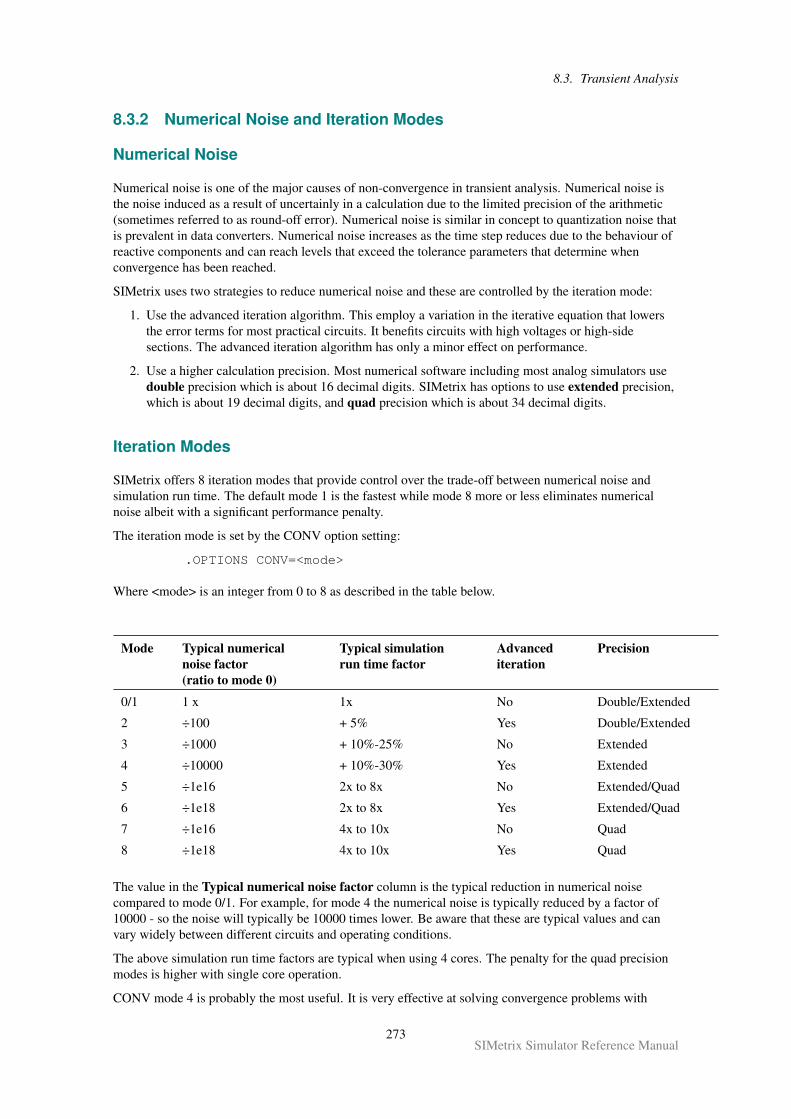
8.3. Transient Analysis
8.3.2 Numerical Noise and Iteration Modes
Numerical Noise
Numerical noise is one of the major causes of non-convergence in transient analysis. Numerical noise isthe noise induced as a result of uncertainly in a calculation due to the limited precision of the arithmetic(sometimes referred to as round-off error). Numerical noise is similar in concept to quantization noise thatis prevalent in data converters. Numerical noise increases as the time step reduces due to the behaviour ofreactive components and can reach levels that exceed the tolerance parameters that determine whenconvergence has been reached.
SIMetrix uses two strategies to reduce numerical noise and these are controlled by the iteration mode:
1. Use the advanced iteration algorithm. This employ a variation in the iterative equation that lowersthe error terms for most practical circuits. It benefits circuits with high voltages or high-sidesections. The advanced iteration algorithm has only a minor effect on performance.
2. Use a higher calculation precision. Most numerical software including most analog simulators usedouble precision which is about 16 decimal digits. SIMetrix has options to use extended precision,which is about 19 decimal digits, and quad precision which is about 34 decimal digits.
Iteration Modes
SIMetrix offers 8 iteration modes that provide control over the trade-off between numerical noise andsimulation run time. The default mode 1 is the fastest while mode 8 more or less eliminates numericalnoise albeit with a significant performance penalty.
The iteration mode is set by the CONV option setting:
.OPTIONS CONV=<mode>
Where <mode> is an integer from 0 to 8 as described in the table below.
Mode Typical numericalnoise factor(ratio to mode 0)
Typical simulationrun time factor
Advancediteration
Precision
0/1 1 x 1x No Double/Extended
2 ÷100 + 5% Yes Double/Extended
3 ÷1000 + 10%-25% No Extended
4 ÷10000 + 10%-30% Yes Extended
5 ÷1e16 2x to 8x No Extended/Quad
6 ÷1e18 2x to 8x Yes Extended/Quad
7 ÷1e16 4x to 10x No Quad
8 ÷1e18 4x to 10x Yes Quad
The value in the Typical numerical noise factor column is the typical reduction in numerical noisecompared to mode 0/1. For example, for mode 4 the numerical noise is typically reduced by a factor of10000 - so the noise will typically be 10000 times lower. Be aware that these are typical values and canvary widely between different circuits and operating conditions.
The above simulation run time factors are typical when using 4 cores. The penalty for the quad precisionmodes is higher with single core operation.
CONV mode 4 is probably the most useful. It is very effective at solving convergence problems with
273SIMetrix Simulator Reference Manual
8.3. Transient Analysis
difficult circuits and affects performance only a little - typically slowing down the simulation by about25%.
Advanced Iteration
Modes 2, 4, 6 and 8 enable advanced iteration employ the advanced iteration algorithm. This uses avariation in the iterative equation that lowers the error terms for most practical circuits. Advanced iterationis mathematically identical to normal iteration and imposes only a marginal performance penalty.
As well as generally having lower numerical noise, advanced iteration has more dependable errordetection. In rare situations, normal iteration can converge on a solution that is inaccurate due to round-offerror. Usually round-off error causes numerical noise as explained above but in linear circuits (or linearportions of non-linear circuits) round-off error can be static which means the convergence detectionalgorithm incorrectly detects an inaccurate result. This effect does not occur with advanced iteration. Thiscan mean that on some occasions advanced iteration fails when normal iteration succeeds.
Note that BSIM4 devices do not support advanced iteration. Any circuit containing such devices will runin normal iteration mode.
Convergence Mode GUI
Modes 0, 2, 4, 6 and 8 may be selected through the convergence GUI. See Users Manual / Analysis Modes/ Convergence / Convergence Options / Iteration Mode
Quad Precision Modes
CONV modes 5 to 8 use Quad precision. Quad precision uses 128-bit values and enjoys a decimalresolution of about 34 digits. No current windows-compatible microprocessor implements quad precisionarithmetic in hardware and consequently quad precision calculations are software implemented.
All quad precision modes enjoy very low levels of numerical noise and more or less eliminate this as asource of transient analysis convergence failure. However the performance penalty can be severe. CONVmode 6 for example, will slow down the simulation typically by about 3x although it can be slower.
Quad precision is not often needed to make a circuit using normal tolerances run; there is usually anotherway to resolve a convergence problem which doesn’t impose a performance penalty. However, if one ofthese setting does fix the problem, it is likely to be a reliable fix, and the increased run time may besatisfactory trade-off.
Quad precision is also useful for diagnosing convergence problems caused by other factors. With the lowerprecision modes, numerical noise can often mask the true cause of a convergence problem. With quadprecision the real cause is more easily seen.
Of the four quad precision modes, mode 6 is likely to the best choice. Mode 6 also makes use of extendedprecision where possible to improve performance and is consequently faster than mode 8 which uses quadprecision exclusively.
Note BSIM4 and the Simkit devices do not support quad precision. Although circuits containing thesedevices will run in quad precision mode, there will only be a small improvement in convergence.
It should be noted that the calculation precision does not usually affect the simulation accuracy. This isdetermined by the tolerance settings especially RELTOL. However, using tighter tolerance parametersincreases the sensitivity of the simulator to the effects of numerical noise and so can, and often does, leadto convergence failure. So, using a higher precision mode will allow tighter values of the toleranceparameters to be used.
274SIMetrix Simulator Reference Manual
8.4. DC Sweep
8.3.3 Fix and Improving Transient Convergence
1. Select menu Simulator | Convergence Failure Report.... This will display a report providinginformation on the cause of failure. For more details of this report, see User’s Manual/AnalysisModes/Convergence/Convergence Failure Report
2. As with DC operating point, check your circuit. In particular, check that you are not doing anythingwhich might cause numerical difficulties such as forward biasing a zero resistance PN junction witha large zero source impedance voltage source.
3. Do anything that will prevent small time steps being needed. Gross non-linearities, regenerativeloops and high gain loops all require small time-steps if not well damped. It may be that you haveleft out damping components to simplify the circuit and speed the simulation.
4. Try a higher iteration mode. At the netlist level add .OPTIONS conv=<value> where <value>is an integer between 2 and 8. The higher the value the higher the precision but the slower thesimulation run time. Modes 5 to 8 use quad precision and have a significant performance penalty.See “Iteration Modes” on page 273 for more details. If running from the schematic editor, somemodes may be selected using menu Simulator | Convergence Options...
5. Avoid over-idealising. A common misconception is that simplifying a circuit by removing reactivecomponents such as capacitors will speed up a simulation and make it easier to converge. Capacitorshave a number of stabilising effects on simulation and are usually beneficial.
6. Avoid using unrealistically large capacitors or inductors and unrealistically small resistors if at allpossible. You should especially avoid such components if non-grounded.
7. If you have some large capacitors in your circuit, try adding a small amount of ESR using thebuilt-in capacitor ESR parameter rather than a separate resistor.
8. If all else fails you can try relaxing some of the tolerances. If your circuit does not have any small(sub-µA) currents then set ABSTOL to 1e-9 or 1e-6. You can also increase VNTOL (default 1e-6)to say 1e-3 if your circuit only has large voltages. Increasing RELTOL is the very last thing youshould try. In our experience, increasing RELTOL beyond its default value (0.001) is rarely areliable solution and can make matters worse.
9. If you have current maintenance, contact technical support providing us with your full schematicand any models you are using. We can fix most convergence problems.
8.4 DC Sweep
DC sweep is basically a repeated DC operating point and so the issues relating to that mode also apply toDC sweep. However, if you are sweeping a voltage or current source, then an altogether better way ofdealing with DC sweep problems is to simulate the DC sweep using transient analysis with a slow ramp.
Using transient analysis to perform DC sweep also resolves problems that can occur with circuits that haveregions where there is more than one stable state e.g. bistables or schmitt triggers. Consider sweeping theinput voltage of a schmitt trigger circuit. When the input voltage is between the lower and upperthresholds, the circuit has two stable states and the DC algorithm could find either of them. As each step ina DC analysis is initialised with the previous step, it will usually find the correct solution but this is notguaranteed. This means that the output could change state even though the input has not passed eitherthreshold. This problem doesn’t occur in transient analysis as in this mode the circuit is running as itwould in real life.
8.5 DC Operating Point Algorithms
SIMetrix uses five alternative strategies to resolve the DC operating point. These are:
275SIMetrix Simulator Reference Manual
8.5. DC Operating Point
1. Junction initialised iteration. This is our name for the standard algorithm sometimes simply knownas ‘DC Iteration’.
2. Source stepping.
3. Diag GMIN stepping.
4. Junction GMIN stepping.
5. Pseudo transient analysis.
These are described in the following sections.
8.5.1 Junction Initialised Iteration
This is the standard algorithm and is sometimes known simply as ‘DC iteration’. Each semiconductorjunction is initialised with a small voltage and iteration then proceeds until convergence (or otherwise).This method often succeeds and is usually the quickest. However, the starting point is only a bit better thanan educated guess and can be so far removed from the real solution that it never has a chance ofsucceeding. (‘Junction initialised iteration’ is a name we have coined and you may see it referred to as JI2elsewhere in this manual and also in messages output by SIMetrix)
8.5.2 Source Stepping
Source stepping. This method - as with all the remaining methods to be described - belong to a class ofconvergence strategies known as continuation methods. These all work by repeating the iterative processwhile gradually varying some circuit parameter. The circuit parameter is chosen so that at its start valuethe solution is known or trivial and at its final value the solution is the operating point that is required. Insource stepping, all the circuit’s power sources are gradually ramped up from zero to their final value.While at zero, the circuit’s solution is trivial; all the voltages and currents are zero. At the first step, thesupplies might be ramped up to 10% of their maximum and the solution iterates to convergence. Then thesupplies are increased and the process is repeated. At each step the solution is initialised with the previoussolution which, if the steps are small, will be close to the new solution that is required and convergencewill therefore be relative easy to achieve.
This method is quite effective and is included in all SPICE based simulators including those derived fromSPICE2. However the SPICE versions use a fixed step size, whereas in SIMetrix (since version 2.0), thestep size is variable so if a step fails, the step size is reduced and it tries again.
However, even with an arbitrarily small step size, this method can fail if the circuit contains some kind ofregenerative action. As the supplies are ramped it is possible for the circuit to abruptly switch from onestate to another as in a schmitt trigger. Although circuits such as schmitt triggers do give difficulty, evencircuits that do not have such elements can also give trouble.
8.5.3 Diagonal GMIN Stepping
In this method, a large conductance term is added to every diagonal entry of the solution matrix andgradually reduced. This is similar to placing a low value resistor from every node of the circuit to groundbut is by no means equivalent. The high conductance term (=low resistance) in the matrix effectivelyswamps non-linearities and as a result the solution is easy to find. The term is gradually reduced until it iszero.
This method is also effective and sometimes works for circuits for which source stepping fails. It isincluded with all SPICE3 derived simulators but, as with source stepping, the SPICE variants use a fixedstep while SIMetrix uses a variable step.
GMIN stepping suffers from the same problems as source stepping but not always with the same circuitsso it always worth trying both approaches.
276SIMetrix Simulator Reference Manual
8.5. DC Operating Point
The received wisdom has always been that GMIN stepping is more effective than source stepping. Thishas not however been borne out by our own research which has shown the source stepping converges moreoften and more quickly. For this reason, SIMetrix attempts source stepping before GMIN stepping. This isthe reverse of SPICE3 and its derivatives.
8.5.4 Junction GMIN Stepping
The junction GMIN stepping method incrementally steps the conductance across semiconductor junctions.This in effect sweeps the GMIN option parameter.
This method is effective for CMOS IC designs as long as GMIN is implemented as a conductance betweendrain and source. This is not the default configuration for LEVEL 1 to 3 MOSFETs in which GMIN isimplemented as two conductances between the drain and bulk and source and bulk. For other MOSFETmodels such as BSIM3, the default GMIN is now between source and drain. For designs containing thesedevices, Junction GMIN Stepping is the first method attempted after JI2. For circuits that do not containsuch devices, this method is not attempted at all.
8.5.5 Pseudo Transient Analysis
This method finds the solution using transient analysis. In SIMetrix, a transient analysis is conductedwhile ramping up all power sources, in effect simulating the action of switching on the power supplies.This is not the same as source stepping as the latter is a pure DC method with all reactive components setto zero. Because reactive components - i.e. capacitors and inductors - are included in transient analysis,effects such as abrupt changes are damped and occur gradually over a finite time. This eliminates theproblem - described above - that the DC continuation methods suffer from.
The above assumes, however, that the circuit is well modelled with all reactive elements correctlyspecified. With integrated circuit design this is usually the case, but for discrete circuits frequently is not.Opamp macro models, for example, consist of many idealised elements that are not always damped byreactive elements. Without such damping, pseudo transient analysis can fail for the same reason as sourceand GMIN stepping. So, SIMetrix automatically adds additional capacitance to the circuit to prevent thissituation from arising.
The end result is a convergence strategy that nearly always succeeds. However, it is generally the slowestmethod so in SIMetrix it is, by default, attempted last.
Although pseudo transient analysis is very powerful it is not completely infallible. Its Achilles Heel isoscillation. Because a transient analysis is being performed it is possible for the circuit to oscillate. If thishappens, pseudo transient analysis can end up going on forever without ever finding a stable solution. Inour experience, however, this is actually rare. A number of steps are taken to damp oscillators so that evencircuits that are designed to oscillate still succeed with pseudo transient analysis.
SIMetrix provides a number of facilities to inhibit circuit oscillation during pseudo transient analysis.These are described in “Pseudo Transient Analysis” on page 269.
8.5.6 Controlling DC Method Sequence
You may have a circuit that only succeeds with - say - pseudo transient analysis and so attempting the othermethods just wastes time. In this situation, you can force the simulator to attempt this method exclusively.To do this you need to set the two simulator options noOpiter and dcopSequence. noOpiter inhibits thefirst method (junction initialised iteration) while dcopSequence controls which and what order theremaining methods are attempted. The value of dcopSequence consists of any combination of SOURCE,GMIN, JUNCGMIN and PTA separated by the pipe symbol: ‘|’. SOURCE, GMIN, JUNCGMIN and PTArefer respectively to ‘source stepping’, ‘DIAG GMIN stepping’, ‘Junction GMIN stepping’ and ‘pseudotransient analysis’. The order in which these words appear in the value of dcopSequence, determines theorder in which the corresponding methods will be attempted. So for example:
277SIMetrix Simulator Reference Manual
8.6. Singular Matrix Errors
.OPTIONS NOOPITER DCOPSEQUENCE=GMIN|PTA
will force GMIN stepping to be attempted first followed by pseudo-transient analysis. Junction initialisediteration, junction GMIN stepping and source stepping won’t be attempted at all. Note that PTA mustalways be the last entry.
8.6 Singular Matrix Errors
A singular matrix error occurs when the circuit does not have a unique and finite solution. For example, acircuit containing a floating capacitor does not have a unique DC solution as the capacitor can be at anyvoltage. Also circuits with shorted inductors, voltage sources or a combination of both will fail with thiserror.
If you get this error, select menu Simulator | Convergence Failure Report. This will show any nodeswith no DC path to ground - a common cause of singular matrix errors. If this doesn’t show the cause,check your circuit generally.
If you think you circuit is OK then it is possible that the error is occurring because during the course ofiterating to a solution, some node voltages or device currents reached very high values and the limitedaccuracy of the machine made it seem that the matrix was singular. This can happen with junctioninitialised iteration. If this is the case, try setting the option:
.OPTIONS NOOPITER
This will inhibit this mode and the simulator will start with source stepping. This method, and the othersthat follow, don’t generally suffer from this problem.
Note that the simulation will abort if a singular matrix is detected in junction initialised iteration. It willnot automatically attempt the other methods. This is because, by far the most common reason for singularmatrices is circuit error.
8.7 Transient Analysis - ‘Time step too small’ Error
The message:
Timestep too small
is not actually due to non-convergence. It means that, because of the nature of your circuit, to achieve therequired accuracy, a time step smaller than the minimum permissible was needed. The default value for theminimum time step is 1e-18 or 1e-9*max-time-step whichever is the smaller. This error can be fixed bysetting a lower value for the minimum time step and can be set in the user interface. See User’sManual/Analysis Modes/Transient Analysis/Setting up a Transient Analysis/Time Step.
8.8 Accuracy and Integration Methods
8.8.1 A Simple Approach
If you wish to increase the accuracy of a simulation, reduce the value of RELTOL. This defaults to 0.001so to reduce it to say 1e-5 add the following line to the netlist:
.OPTIONS RELTOL=1e-5
278SIMetrix Simulator Reference Manual
8.8. Accuracy, Integration
(The setting of RELTOL is supported by the front end. See User’s Manual/Analysis Modes/SimulatorOptions/Setting Simulator Options/Tolerances for details.)
The simulation will run slower. It might be a lot slower it might be only slightly slower. In veryunfortunate circumstances it might not simulate at all and fail with a convergence error.
Conversely, you can speed up the simulation by increasing RELTOL but you should not set this to a valuehigher than around 0.005 as this will degrade accuracy to an unacceptable level.
8.8.2 Iteration Accuracy
For DC and transient modes, the simulator essentially makes an approximation to the true answer. For DCanalysis an iterative method is used to solve the non-linear equations which can only find the exact answerif the circuit is linear. The accuracy of the result for non-linear circuits is determined by the number ofiterations; accuracy is improved by performing more iterations but obviously this takes longer. In order tocontrol the number of iterations that are performed an estimate is made of the error by comparing twosuccessive iterations. When this error falls below a predetermined tolerance, the iteration is deemed tohave converged and the simulator moves on the next step or completes the run. Most SPICE simulators usesomething similar to the following equations to calculate the tolerance:
For voltages: TOL = RELTOL * instantaneous_value + VNTOL
For currents: TOL = RELTOL * instantaneous_value + ABSTOL
"instantaneous_value" is the larger of the current and previous iterations. VNTOL has a default value of1µV so for voltages above 1mV, RELTOL dominates. ABSTOL has a default of 1pA so for currents above1nA, RELTOL dominates.
The above method of calculating tolerance works fine for many circuits using the default values of VNTOLand ABSTOL. However, SPICE was originally designed for integrated circuit design where voltages andcurrents are always small, so the default values of ABSTOL and VNTOL may not be appropriate for - say- a 100V 20A power supply. Suppose, that such a PSU has a current that rises to 20A at some point in thesimulation, but falls away to zero. When at 20A it has a tolerance of 20mA but when it falls to zero thetolerance drops to ABSTOL which is 1pA. In most situations the 1pA tolerance would be absurdly tightand would slow down the simulation. Most other SPICE products recommend increasing ABSTOL andVNTOL for PSU circuits and indeed this is perfectly sound advice. However, In SIMetrix the toleranceequation has been modified to make this unnecessary in most cases. Here is the modified equation:
For voltages: TOL = RELTOL * MAX( peak_value * POINTTOL, instantaneous_value ) + VNTOL
For currents: TOL = RELTOL * MAX( peak_value * POINTTOL, instantaneous_value ) + ABSTOL
peak_value is the magnitude of the largest voltage or current encountered so far for the signal under test.POINTTOL is a new tolerance parameter and has a default value of 0.001. So for the example we gaveabove, peak_value would be 20 and when instantaneous_value falls to zero the tolerance would be:
0.001 * MAX(20 * 0.001, 0) + 1p = approx. 20µA
20µA is a much more reasonable tolerance for a signal that reaches 20A.
The above method has the advantage that it loosens the tolerance only for signals that actually reach largevalues. Parts of a circuit that only see small voltages or currents - such as the error amplifier of aservo-controlled power supply - would still be simulated with appropriate precision.
POINTTOL can be increased to improve simulation speed. It is a more controlled method than increasingRELTOL. POINTTOL can be raised to 0.1 or even 1.0 but definitely no higher than 1.0.
8.8.3 Time Step Control
The tolerance options mentioned above also affect the time step control algorithm used in transientanalysis. In SIMetrix, there are three mechanisms that control the time step, one of which has to be
279SIMetrix Simulator Reference Manual
8.8. Accuracy, Integration
explicitly enabled. These are:
1. Iteration time step control
2. LTE time step control
3. Voltage delta limit
Item 3 above is inactive unless explicitly enabled using the MAXVDELTAREL option setting. See belowfor details.
Iteration Time Step Control
Iteration control reduces the time step by a factor of 8 if convergence to the specified accuracy cannot beachieved after 10 iterations. (10 by default but can be changed with ITL4 option). If convergence issuccessful, the time step is doubled. As this mechanism is controlled by the success or otherwise of theiteration it is also affected by the same tolerance options described in the above section about iterationaccuracy.
LTE Time Step Control
"LTE time step control" is an algorithm which controls the accuracy of the numerical integration methodused to model reactive devices such as inductors and capacitors. These devices are governed by adifferential equation. It is not possible in a non-linear circuit to solve these differential equations exactly soa numerical method is used and this - like the iterative methods used for non-linear devices - isapproximate. In the case of numerical integration, the accuracy is determined by the time step. Thesmaller the time step the greater the accuracy but also the longer the simulation time.
The accuracy to which capacitors are simulated is controlled by RELTOL, POINTTOL and two otheroptions namely TRTOL and CHGTOL. The latter is a charge tolerance and has a similar effect to VNTOLand ABSTOL but instead represents the charge in the capacitor. It’s default value is 1e-14 which, likeABSTOL and VNTOL is appropriate for integrated circuits but may be too low for PSU circuits with largecapacitors. However, the peak detection mechanism controlled by POINTTOL described in the abovesection also works for the LTE time step control algorithm and it is therefore rarely necessary to alterCHGTOL.
TRTOL is a dimensionless value which defaults to 7. It affects the overall accuracy of the numericalintegration without affecting the precision of the iteration. So reducing TRTOL will increase the accuracywith which capacitors and inductors are simulated without affecting the accuracy of the iterative methodused to simulate non-linear elements. However, in order for the simulation of reactive devices to beaccurate, the non-linear iteration must also be accurate. So, reducing TRTOL much below unity will resultin a longer simulation time but no improvement in precision. Increasing TRTOL to a large value, however,may be appropriate in some circumstances where the accuracy to which reactive devices are simulated isnot that important. This may be the case in a circuit where there is an interest in the steady state but not inhow it was reached.
Inductors are controlled by the same tolerances except CHGTOL is replaced by FLUXTOL. This defaultsto 1e-11.
The default LTE time step algorithm used in SIMetrix is slightly different to that used by standard SPICE.The standard SPICE variant is also affected by ABSTOL and VNTOL. The SIMetrix algorithm controlsthe time step more accurately and as a result offers better speed-accuracy performance.
Voltage Delta Limit
This places a limit on the amount of change allowed in a single timestep for each node. This limit isgoverned by the option setting MAXVDELTAREL and MAXVDELTAABS and is included to overcome a
280SIMetrix Simulator Reference Manual
8.8. Accuracy, Integration
problem that can cause false clocking of flip-flops. The limit can be calculated from:
MAXVDELTAABS + MAXVDELTAREL*(node_voltage)
where node_voltage is the larger of the node voltage at current time step and the node voltage at theprevious time step. The above is calculated for all voltage nodes. If the change in voltage exceeds thislimit, the time step is cut back.
The above mechanism is not enabled if MAXVDELTAREL is zero or less and MAXVDELTAREL is zeroby default.
Setting MAXVDELTAREL to a value of about 0.4 will usually fix problems of false clocking in flip-flops.However, this will slow down the simulation slightly and it is not recommended that this setting is used incircuits that do not contain flip-flops.
8.8.4 Accuracy of AC analyses
The small-signal analysis modes .AC, .TF and .NOISE do not use approximate methods and their accuracyis limited only by the precision of the processor’s floating point unit. Of course the DC operating point thatalways precedes these analysis modes is subject to the limitations described above. Also, the devicemodels used for non-linear devices are also in themselves approximations. So these modes should not beseen as exact but they are not affected by any of the tolerance option settings.
8.8.5 Summary of Tolerance Options
RELTOL
Default = 0.001. This affects all DC and transient simulation modes and specifies the relative accuracy.Reduce this value to improve precision at the expense of simulation speed. We do not recommendincreasing this value except perhaps to run a quick test. In any case, you should never use a value largerthan 0.01.
POINTTOL
Proprietary to SIMetrix. Default = 0.001. Can increase to a maximum of 1.0 to improve speed with loss ofprecision. Reduce to 0 for maximum accuracy but note this may just slow down the simulation withoutreally improving precision where it is needed.
ABSTOL
Default = 1pA. This is an absolute tolerance for currents and therefore has units of Amps. This basicallyaffects the tolerance for very low values of current. Sometimes worth increasing to resolve convergenceproblems or improve speed for power circuits.
VNTOL
Default = 1V. Same as ABSTOL but for voltages.
281SIMetrix Simulator Reference Manual
8.8. Accuracy, Integration
TRTOL
Default = 7. This is a relative value and affects how accurately charge storage elements are simulated.Reduce it to increase accuracy of reactive elements but there is no benefit reducing below about 1.0. Incircuits where there is more interest in the steady state rather than how to get there, simulation speed canbe improved by increasing this value.
CHGTOL
Default = 1e-14. Minimum tolerance of capacitor charge. Some convergence and speed improvement maybe gained by increasing this for circuits with large capacitors. Generally recommended to leave it alone.
FLUXTOL
Default = 1e-11. Same as CHGTOL except applied to inductors.
8.8.6 Integration Methods - METHOD option
SIMetrix, along with most other SPICE products use three different numerical integration methods tomodel reactive elements such as capacitors and inductors. These are Backward Euler, Trapezoidal Ruleand Gear. Backward Euler is used unconditionally at various times during the course of a simulation but atall other times the method used is controlled by the METHOD option (as long as ORDER is set to 2 orhigher - see below).
The METHOD option can be set to TRAP (trapezoidal - the default) or GEAR. Gear integration can solvea common problem whereby the solution seems to oscillate slightly. An example is shown below.
282SIMetrix Simulator Reference Manual
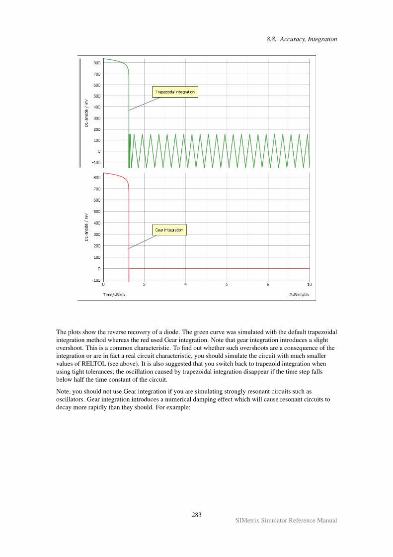
8.8. Accuracy, Integration
The plots show the reverse recovery of a diode. The green curve was simulated with the default trapezoidalintegration method whereas the red used Gear integration. Note that gear integration introduces a slightovershoot. This is a common characteristic. To find out whether such overshoots are a consequence of theintegration or are in fact a real circuit characteristic, you should simulate the circuit with much smallervalues of RELTOL (see above). It is also suggested that you switch back to trapezoid integration whenusing tight tolerances; the oscillation caused by trapezoidal integration disappear if the time step fallsbelow half the time constant of the circuit.
Note, you should not use Gear integration if you are simulating strongly resonant circuits such asoscillators. Gear integration introduces a numerical damping effect which will cause resonant circuits todecay more rapidly than they should. For example:
283SIMetrix Simulator Reference Manual
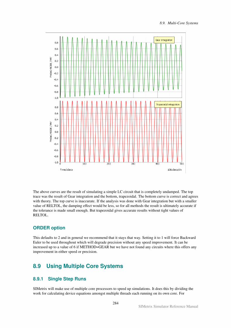
8.9. Multi-Core Systems
The above curves are the result of simulating a simple LC circuit that is completely undamped. The toptrace was the result of Gear integration and the bottom, trapezoidal. The bottom curve is correct and agreeswith theory. The top curve is inaccurate. If the analysis was done with Gear integration but with a smallervalue of RELTOL, the damping effect would be less, so for all methods the result is ultimately accurate ifthe tolerance is made small enough. But trapezoidal gives accurate results without tight values ofRELTOL.
ORDER option
This defaults to 2 and in general we recommend that it stays that way. Setting it to 1 will force BackwardEuler to be used throughout which will degrade precision without any speed improvement. It can beincreased up to a value of 6 if METHOD=GEAR but we have not found any circuits where this offers anyimprovement in either speed or precision.
8.9 Using Multiple Core Systems
8.9.1 Single Step Runs
SIMetrix will make use of multiple core processors to speed up simulations. It does this by dividing thework for calculating device equations amongst multiple threads each running on its own core. For
284SIMetrix Simulator Reference Manual
8.10. Matrix Solver
example, a circuit with 100 transistors will need the equations governing the transistors to be calculated foreach iteration. With a 4 core system, each core can be assigned the equations for 25 transistors to becalculated in parallel which will allow the iteration to complete in less time.
However, only the device equation calculation is subject to multiple core execution. There are many othertasks that are performed during a simulation run that remain single-threaded, that is executed in sequenceon a single core. For this reason multiple cores will not give a speed up proportional to the number ofcores.
8.9.2 Using Multiple Cores for Single Step Runs
SIMetrix will automatically choose how many cores to use for the simulation. For simple circuits it willuse a single core and beyond a certain level of complexity it will use all the cores available on a singlechip. So if you have a 4-core machine where all 4 cores are implemented on a single processor chip,SIMetrix will use all 4 cores as long as the circuit complexity is sufficient to justify it.
If you have a machine with, for example, 8 cores implemented using 2 4-core processor ICs, SIMetrix willuse just one of the ICs so therefore 4 cores.
You can override the number of cores using the mpnumthreads .OPTIONS setting. E.g.:
.OPTIONS MPNUMTHREADS=2
will force 2 cores to be used as long as the computer system does actually have 2 cores. SIMetrix will notuse more threads than there are physical cores available.
Be aware that hyperthreaded logical processors are not counted as a physical processor. So if you have 4physical cores and 8 logical cores implemented using hyperthreading, SIMetrix will use a maximum of 4cores.
8.9.3 Multi-core Multi-step Simulation
Multiple core execution does give a very substantial speed improvement when applied to multi-stepanalyses. This is covered in User’s Manual/Analysis Modes/Multi-step Analyses/Using Multiple Cores forMulti-step Analyses.
8.10 Matrix Solver
To simulate a circuit, SIMetrix formulates a set of linear equations from the non-linear equations thatgovern the devices in the circuit. This is part of an iterative algorithm that is repeated successively toconverge on the solution to the non-linear system. The linear system of equations is solved using a matrixsolver.
SIMetrix has two matrix solvers and you can choose between them. The two solvers are:
1. Sparse 1.3 developed by Kenneth Kundert and which is the solver supplied with SPICE 3
2. KLU developed by a research group at the University of Florida under Prof. Tim Davis. This wasdeveloped for circuit simulation and was moulded to perform well for the type of matrix that circuitsimulators tend to generate. The solver makes use of more modern techniques than the originalSPICE3 solver which was developed in the 1980s.
SIMetrix uses KLU by default and for most applications this is the better choice. For circuits with morethan about 500 nodes it is almost always faster for the following reasons:
1. It has uses superior ordering algorithms. The matrix that arises from circuit simulation problems issparse which means that nearly all terms are zero. Exploiting sparsity to greatest effect depends on
285SIMetrix Simulator Reference Manual

8.10. Matrix Solver
the row and column ordering. KLU makes use of modern research to produce superior ordering toSparse 1.3
2. The factorisation algorithm is superior
3. It can be reordered efficiently and rapidly. The optimum matrix ordering that is ideal for DC andlong time steps is often different to that needed for small time steps. Sparse 1.3 can not be reorderedvery efficiently and tends to use the same ordering throughout the simulation. KLU can be reorderedmuch more frequently providing optimal ordering at all times
Although KLU is usually the best choice, Sparse 1.3 can give better results for small circuits. To changethe matrix solver use this option:
.options spsolver=solver
Where solver is:
KSPARSE for Sparse 1.3
or
KLU for KLU
Currently .SENS analyses always use Sparse 1.3 regardless of the spsolver setting.
286SIMetrix Simulator Reference Manual
9.2. Logic States
Chapter 9
Digital Simulation
9.1 Overview
As well as an analog simulator, SIMetrix incorporates an event driven digital simulator tightly coupled tothe analog portion. This system can rapidly and accurately simulate mixed signal circuits containing bothanalog and digital components. Of course, an analog only simulator can simulate a mixed signal circuitusing digital models constructed from analog components, but this approach is slow. The advantage of thismixed-mode approach is that it is dramatically faster, typically in the order of 100 times for pure digitalcircuits.
The SIMetrix mixed mode simulator is based on the XSPICE system developed by the Georgia TechnicalResearch Institute. Although based on XSPICE, SIMetrix features many enhancements over the originalsystem. See “Enhancements over XSPICE” on page 309 for details of these improvements.
If you only use digital models supplied in the device library, then you don’t need to know much about thedigital simulator in order to use it. Just select the devices you need from the parts browser and simulate inthe normal way. This chapter describes some of the inner workings of the simulator including how itinterfaces to the analog system. More importantly, perhaps, this chapter also describes how you can designyour own digital models.
9.2 Logic States
The digital simulator is described as ‘12-state’ which means that a digital signal can be in 1 of 12 states.These 12 states are combined from 3 levels and 4 strengths as follows:
Logic levels Strengths
HIGH STRONG
LOW RESISTIVE
UNKNOWN HI-IMPEDANCE
UNDETERMINED
Logic levels HIGH and LOW are self-explanatory. UNKNOWN means the signal could be either HIGH orLOW but which is not known at this stage. The start up state of a flip-flop is an example of anUNKNOWN state. Strength refers to the driving force behind the signal. STRONG is the highest withHI-IMPEDANCE the lowest. It is used to resolve conflicts when two outputs are connected together. Forexample consider a LOW-RESISTIVE signal (as possessed by a pull-down resistor) connected to a
287SIMetrix Simulator Reference Manual
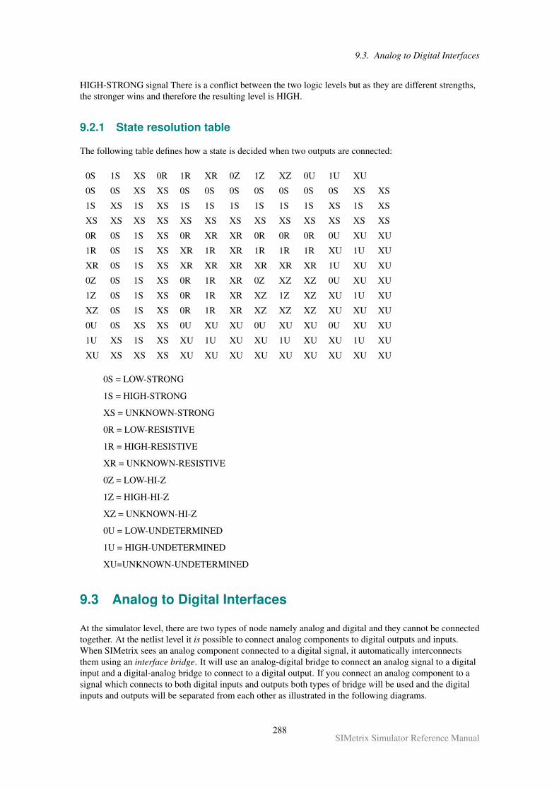
9.3. Analog to Digital Interfaces
HIGH-STRONG signal There is a conflict between the two logic levels but as they are different strengths,the stronger wins and therefore the resulting level is HIGH.
9.2.1 State resolution table
The following table defines how a state is decided when two outputs are connected:
0S 1S XS 0R 1R XR 0Z 1Z XZ 0U 1U XU
0S 0S XS XS 0S 0S 0S 0S 0S 0S 0S XS XS
1S XS 1S XS 1S 1S 1S 1S 1S 1S XS 1S XS
XS XS XS XS XS XS XS XS XS XS XS XS XS
0R 0S 1S XS 0R XR XR 0R 0R 0R 0U XU XU
1R 0S 1S XS XR 1R XR 1R 1R 1R XU 1U XU
XR 0S 1S XS XR XR XR XR XR XR 1U XU XU
0Z 0S 1S XS 0R 1R XR 0Z XZ XZ 0U XU XU
1Z 0S 1S XS 0R 1R XR XZ 1Z XZ XU 1U XU
XZ 0S 1S XS 0R 1R XR XZ XZ XZ XU XU XU
0U 0S XS XS 0U XU XU 0U XU XU 0U XU XU
1U XS 1S XS XU 1U XU XU 1U XU XU 1U XU
XU XS XS XS XU XU XU XU XU XU XU XU XU
0S = LOW-STRONG
1S = HIGH-STRONG
XS = UNKNOWN-STRONG
0R = LOW-RESISTIVE
1R = HIGH-RESISTIVE
XR = UNKNOWN-RESISTIVE
0Z = LOW-HI-Z
1Z = HIGH-HI-Z
XZ = UNKNOWN-HI-Z
0U = LOW-UNDETERMINED
1U = HIGH-UNDETERMINED
XU=UNKNOWN-UNDETERMINED
9.3 Analog to Digital Interfaces
At the simulator level, there are two types of node namely analog and digital and they cannot be connectedtogether. At the netlist level it is possible to connect analog components to digital outputs and inputs.When SIMetrix sees an analog component connected to a digital signal, it automatically interconnectsthem using an interface bridge. It will use an analog-digital bridge to connect an analog signal to a digitalinput and a digital-analog bridge to connect to a digital output. If you connect an analog component to asignal which connects to both digital inputs and outputs both types of bridge will be used and the digitalinputs and outputs will be separated from each other as illustrated in the following diagrams.
288SIMetrix Simulator Reference Manual
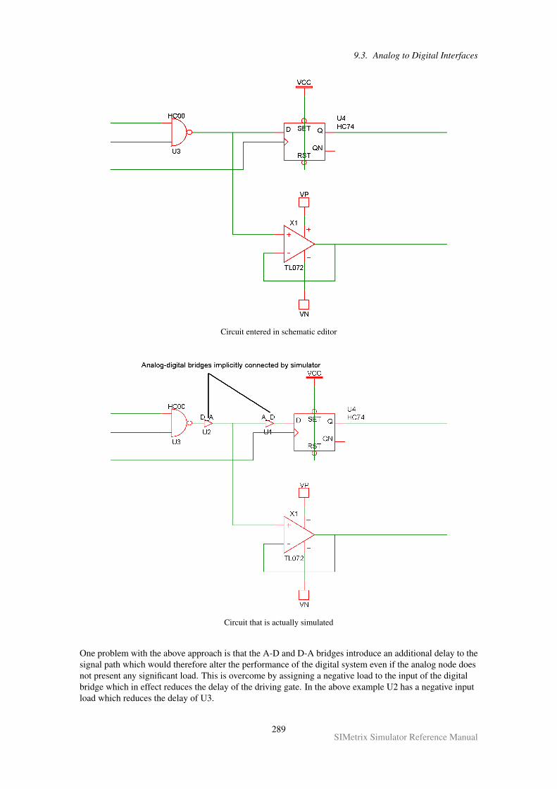
9.3. Analog to Digital Interfaces
Circuit entered in schematic editor
Circuit that is actually simulated
One problem with the above approach is that the A-D and D-A bridges introduce an additional delay to thesignal path which would therefore alter the performance of the digital system even if the analog node doesnot present any significant load. This is overcome by assigning a negative load to the input of the digitalbridge which in effect reduces the delay of the driving gate. In the above example U2 has a negative inputload which reduces the delay of U3.
289SIMetrix Simulator Reference Manual
9.4. Logic Families
9.3.1 How A-D Bridges are Selected
When SIMetrix implicitly places an AD bridge in a circuit, it must choose an appropriate model for thebridge. All AD bridges are based on DAC_BRDIGE and ADC_BRIDGE models described in“Analog-Digital Interface Bridge” on page 176, and “Digital-Analog Interface Bridge” on page 183. Themodel is chosen according to the FAMILY parameter assigned to the digital device to which the bridge isconnected. The FAMILY parameter along with the associated OUT_FAMILY and IN_FAMILYparameters are explained more fully in “Logic families” on page 290. Basically the FAMILY parameterspecifies the logic family to which the device belongs e.g. ‘HC’ for high speed CMOS.
The name of the model used to interconnect digital to analog is always of the form:
family_name_dac
and to interconnect analog to digital
family_name_adc
For example if the family name is HC the D-A bridge is called HC_DAC. There is a selection of A-D andD-A bridges in the model library supplied with SIMetrix. (In BRIDGES.LB).
9.4 Logic Families
The digital simulator only knows about the 12 logic states described in “Logic States” on page 287. Itdoesn’t know anything about threshold voltages or output impedances and consequently cannot directlyhandle the effects of interconnecting devices from different logic families. It does however feature amechanism of determining the level of compatibility between families and will raise an error ifincompatible devices are interconnected. For example, ECL and high speed CMOS operate at completelydifferent thresholds and cannot be connected except via a special interface gate. SIMetrix knows this sothat if you attempt to connect such devices, an error message will be displayed and the simulation will notrun. Conversely, it is perfectly OK to drive an LSTTL input from an HC output and SIMetrix will operatenormally if you do so. If you drive an HC input from an LSTTL output SIMetrix will issue a warning as,although this may work in practice, it cannot be guaranteed to do so under all circumstances.
Another problem arises when connecting inputs from different logic families together. SIMetrix deals withthis by treating groups of inputs as if they were all from the same logic family provided they arecompatible. This selected logic family is then used to resolve any output-input conflict as described above.It is also used to select an analog-digital interface bridge as described in “Analog to Digital Interfaces” onpage 288.
Groups of outputs from different families are dealt with in the same way as inputs described above.
SIMetrix knows how to resolve these situations by referring to a set of three tables called the ‘LogicCompatibility Tables’. A standard set of tables is built in to the simulator but they can also be redefined.See “Logic Compatibility Tables” on page 291.
9.4.1 Logic Family Model Parameters.
There are three model parameters used to specify the logic family to which a device belongs. These are:
Parameter name Description
IN_FAMILY Family for inputs
OUT_FAMILY Family for outputs
FAMILY Family for both inputs and outputs if IN_FAMILY/OUT_FAMILY notspecified
290SIMetrix Simulator Reference Manual

9.4. Logic Families
The parameters are text strings. Any name may be used that is defined in the logic compatibility tables butyou must not use the underscore character in a family name. The families supported by the internal tablesare listed in “Supported Logic Families” on page 292.
The underscore character is used to define a sub-family that has the same characteristics as the main familyas far as logic compatibility is concerned but which will call a different interface bridge when connected toan analog node. This is used to define schmitt trigger devices such as the 74HC14. In an all-digital circuitthis behaves exactly like a normal inverter with a slightly longer delay. When the input is connected to ananalog system an interface bridge with the appropriate hysteresis is called up instead of the normalinterface.
9.4.2 Logic Compatibility Tables
As explained in the above section, there are three of these. Each table has a row and column entry for eachof the logic families supported. These are:
• Resolve In-Out table. Decides what to do when an output is connected to an input from a differentfamily. Possible responses are OK, ERR (error - not permissible) and WARN (OK but give warningto user)
• Resolve In-In table. Decides how to treat the situation when two inputs from dissimilar families areconnected. As described above SIMetrix must treat a group of inputs connected together as allbelonging to the same logic family for the purpose of deciding an analog interface bridge (see“Analog to Digital Interfaces” on page 288) and to resolve in-out family conflicts. Possibleresponses are ROW, COLUMN and ERR. ROW means that the family defining the ROW entry haspriority and COLUMN means that the family defining the COLUMN entry has priority. ERR meansthat it is an error to interconnect these two inputs. You can also enter OK which signifies that thetwo families are equivalent and it doesn’t matter which is chosen. Currently this response is exactlyequivalent to ROW.
• Resolve Out-Out table. Works the same way as the Resolve In-In table but used to define outputpriorities.
The tables can be redefined by specifying a file containing the new definition. If running in GUI mode anew file can be specified at any time using the ReadLogicCompatibility command (Script ReferenceManual/Function Reference/ReadLogicCompatibility). It can also be specified as the configuration settingCompatTable. The format of this file is described in the following section.
9.4.3 Logic Compatibility File Format
For an example of a compatibility table, see the file COMPAT.TXT which you will find in the SCRIPTdirectory. This file is actually identical to the built-in definitions except for the UNIV family which cannotbe redefined.
The file format consists of the following sections:
1. Header
2. In-Out resolution table
3. In-In resolution table
4. Out-Out resolution table
Header
The names of all the logic families listed in one line. The names must not use the underscore (‘_’)character.
291SIMetrix Simulator Reference Manual

9.4. Logic Families
In-Out resolution table:
A table with the number of rows and columns equal to the number of logic families listed in the header.The columns represent outputs and the rows inputs. The entry in the table specifies the compatibilitybetween the output and the input when connected to each other. The entry may be one of three values:
Value Meaning
OK Fully compatible
WARN Not compatible but would usually function. Warn user but allow simulation to continue.
ERR Not compatible and would never function. Abort simulation.
In-In resolution table
A table with the number of rows and columns equal to the number of logic families listed in the header.Both column and rows represent inputs. The table defines how inputs from different families are treatedwhen they are connected. The entry may be one of four values:
Value Meaning
ROW Row take precedence
COL Column takes precedence
OK Doesn’t matter. (Currently identical to ROW)
ERR Incompatible, inputs cannot be connected.
Out-out resolution table
A table with the number of rows and columns equal to the number of logic families listed in the header.Both column and rows represent outputs. The table defines how outputs from different families are treatedwhen they are connected. The entry may be one of four values:
Value Meaning
ROW Row take precedence
COL Column takes precedence
OK Doesn’t matter. (Currently identical to ROW)
ERR Incompatible, outputs cannot be connected.
9.4.4 Supported Logic Families
The following logic families are supported by the internal Logic Compatibility Tables.
Family name Description
TTL TTL - 74 series
292SIMetrix Simulator Reference Manual
9.5. Load Delay
Family name Description
HC High speed CMOS - 74HC series
HCT TTL compatible High speed CMOS - 74HCT series
FAST FAST TTL - 74F series
LS Low power schottky TTL - 74LS series
ALS Advanced low power schottky TTL - 74ALS series
4000-5 4000 series CMOS - 5V operation
4000-10 4000 series CMOS - 10V operation
4000-15 4000 series CMOS - 15V operation
ECL10K ECL 10K series
ECL10KE ECL Eclipse series
AC Advanced CMOS - 74AC series
ACT TTL compatible Advanced CMOS - 74ACT series
FORCE5 Used for 5V VCC rails.
UNIV Universal family - see below
9.4.5 Universal Logic Family
The internal tables support the concept of a ‘Universal logic family’. This is called UNIV and can connectto any logic family without error. This is the default if no FAMILY parameter is supplied.
9.4.6 Internal Tables
The internal tables are documented in the on-line help system. Refer to topic “Internal Tables” which islisted as a keyword in the index tab.
9.5 Load Delay
9.5.1 Overview
The digital simulator includes mechanisms to model the delay introduced when an output is loaded. Twosources of delay are provided for, namely ‘input delay’ and ‘wire delay’. Input delay is determined by thecapacitive input while wire delay is an additional delay caused by the capacitance of the interconnection.
Both input delay and wire delay are affected by the driving outputs ‘resistance’.
9.5.2 Output Resistance
Most devices that have digital outputs have three parameters to define output resistance. Note that theresistance we are referring to here is not an actual analog resistance but a conceptual value that whenmultiplied by load capacitance provides a delay value.
The three output resistance parameters are: out_res, out_res_pos, out_res_neg. out_res_pos andout_res_neg define the output resistance for positive and negative transitions respectively. out_res providesa default value for out_res_pos and out_res_neg.
293SIMetrix Simulator Reference Manual
9.6. Digital Model Libraries
9.5.3 Input Delay
Most digital inputs include an ‘input_load’ capacitance parameter. The total input delay is obtained bymultiplying the sum of all connected input capacitances by the driving output’s output resistance asdescribed above.
9.5.4 Wire Delay
Wire delay is derived from the number of connected inputs following a non-linear relationship defined in alook-up table.
Defining Look-up Table
The wire delay look-up table must be defined in a file containing pairs of values with one pair per line. Thefirst value in the pair is the number of connections and the second is the capacitance. For example:
0 01 02 1e-125 10e-1210 30e-12
Linear interpolation is used to derive missing values.
To specify the wire table used for a simulation, add the line:
.OPTIONS WireTable=filename
where filename is the path of the wire table file.
9.6 Digital Model Libraries
9.6.1 Using Third Party Libraries
The SIMetrix digital simulator is based on XSPICE and all the XSPICE digital devices have beenimplemented. Virtually all of these have been enhanced in a number of ways but all remain backwardcompatible with the original XSPICE. Consequently any 100% XSPICE compatible digital model willwork with SIMetrix.
9.7 Arbitrary Logic Block - User Defined Models
9.7.1 Overview
The arbitrary logic block is an internal component that can be defined to perform any logic function. Usinga simple descriptive language it is possible to define combinational logic elements, synchronous andasynchronous registers as well as look-up table (ROMs) and arrays (RAMs).
Each ALB device is defined as a normal .MODEL statement which refers to a separate file containing thelogic description. This section is mostly concerned with the descriptive language used in the definition file.
294SIMetrix Simulator Reference Manual
9.7. Arbitrary Logic Block - User Defined Models
9.7.2 An Example
We start with a simple example. The following is a description of a simple 8 bit synchronous counter.(This definition would be put into a file referred to in a .MODEL statement. This is described later). Acircuit using this model is supplied as an example. See EXAMPLES/ALB_Examples/count.sch
PORT (DELAY = 10n) CountOut out[0:7] ;EDGE (DELAY=5n, WIDTH=8, CLOCK=in[0]) Count ;Count = Count + 1 ;CountOut = count ;
We will go through this line by line.
The first line:
PORT (DELAY = 10n) CountOut out[0:7] ;
is a PORT statement and in this case defines the characteristics of an output.
(DELAY = 10n)
says that the output delay is 10nS that is the actual output pins will change state 10nS after the output isassigned.
CountOut
names the output CountOut.
out[0:7]
defines the port as an output and specifies the actual pins used on the device. This specifies the first 8 pinson the output port. There are two sets of pins on an ALB one assigned for inputs and referred to as"in[a:b]" and the other assigned for outputs and referred to as "out[a:b]". The line ends in a semi-colonwhich terminates the statement. All statements must end in a semi-colon.
The next line:
EDGE (DELAY=5n, WIDTH=8, CLOCK=in[0]) Count ;
defines an edge triggered register.
CLOCK=in[0]
specifies the pin used for the clock (it must always be an input pin). This is always positive edge triggered.
DELAY=5n
This is the clock to output delay. (See illustration below)
WIDTH=8
This specifies the width of the register i.e. 8 bits
The next line:
Count = Count + 1 ;
defines the operation to be performed at each clock edge. In this case the value in the register is simplyincremented by one. When it reaches 255 it will reset to 0.
The final line
CountOut = count ;
295SIMetrix Simulator Reference Manual
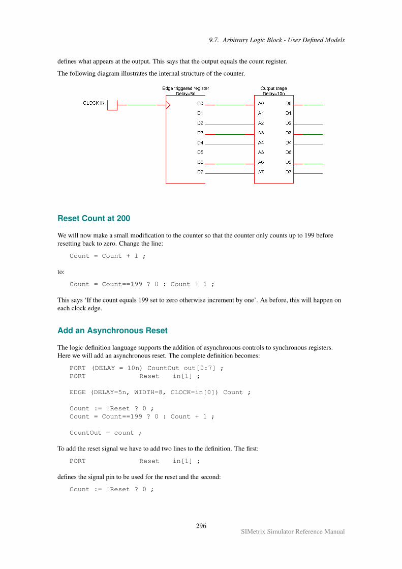
9.7. Arbitrary Logic Block - User Defined Models
defines what appears at the output. This says that the output equals the count register.
The following diagram illustrates the internal structure of the counter.
Reset Count at 200
We will now make a small modification to the counter so that the counter only counts up to 199 beforeresetting back to zero. Change the line:
Count = Count + 1 ;
to:
Count = Count==199 ? 0 : Count + 1 ;
This says ‘If the count equals 199 set to zero otherwise increment by one’. As before, this will happen oneach clock edge.
Add an Asynchronous Reset
The logic definition language supports the addition of asynchronous controls to synchronous registers.Here we will add an asynchronous reset. The complete definition becomes:
PORT (DELAY = 10n) CountOut out[0:7] ;PORT Reset in[1] ;
EDGE (DELAY=5n, WIDTH=8, CLOCK=in[0]) Count ;
Count := !Reset ? 0 ;Count = Count==199 ? 0 : Count + 1 ;
CountOut = count ;
To add the reset signal we have to add two lines to the definition. The first:
PORT Reset in[1] ;
defines the signal pin to be used for the reset and the second:
Count := !Reset ? 0 ;
296SIMetrix Simulator Reference Manual
9.7. Arbitrary Logic Block - User Defined Models
defines the action to be taken. This is an asynchronous action statement. The ‘!’ means NOT so the linesays ‘If Reset is NOT TRUE (i.e. low) set the count to zero otherwise do nothing’. Asynchronous actionstatements are always of the form:
register_name := condition ? action ;
The ‘:’ signifies that the statement is asynchronous and that the action should happen immediately.
9.7.3 Example 2 - A Simple Multiplier
PORT (DELAY=10n) MultOut out[0:7] ;PORT in1 in[0:3] ;PORT in2 in[4:7] ;
MultOut = in1*in2 ;
The above defines a simple combinational circuit, that of a 4X4 digital multiplier. The inputs in1 and in2are treated as 4 bit unsigned values so if both are zero the output will be zero and if both are 1111 (i.e. 15)the result will be 11100001 (i.e. 225). See the circuit EXAMPLES/ALB_Examples/Mult.sch.
9.7.4 Example 3 - A ROM Lookup Table
The following definition is that of a lookup table to define a sine wave:
PORT (DELAY=10n) ROMout out[0:7] ;PORT input in[0:7] ;
READONLY (WIDTH=8) ROM[256] =
128, 131, 134, 137, 140, 143, 146, 149, 152, 156, 159, 162,165, 168, 171, 174, 176, 179, 182, 185, 188, 191, 193, 196,199, 201, 204, 206, 209, 211, 213, 216, 218, 220, 222, 224,226, 228, 230, 232, 234, 236, 237, 239, 240, 242, 243, 245,246, 247, 248, 249, 250, 251, 252, 252, 253, 254, 254, 255,255, 255, 255, 255, 255, 255, 255, 255, 255, 255, 254, 254,253, 252, 252, 251, 250, 249, 248, 247, 246, 245, 243, 242,240, 239, 237, 236, 234, 232, 230, 228, 226, 224, 222, 220,218, 216, 213, 211, 209, 206, 204, 201, 199, 196, 193, 191,188, 185, 182, 179, 176, 174, 171, 168, 165, 162, 159, 156,152, 149, 146, 143, 140, 137, 134, 131, 128, 124, 121, 118,115, 112, 109, 106, 103, 99, 96, 93, 90, 87, 84, 81, 79, 76,73, 70, 67, 64, 62, 59, 56, 54, 51, 49, 46, 44, 42, 39, 37,35, 33, 31, 29, 27, 25, 23, 21, 19, 18, 16, 15, 13, 12, 10,9, 8, 7, 6, 5, 4, 3, 3, 2, 1, 1, 0, 0, 0, 0, 0, 0, 0, 0, 0,0, 0, 1, 1, 2, 3, 3, 4, 5, 6, 7, 8, 9, 10, 12, 13, 15, 16,18, 19, 21, 23, 25, 27, 29, 31, 33, 35, 37, 39, 42, 44, 46,49, 51, 54, 56, 59, 62, 64, 67, 70, 73, 76, 79, 81, 84, 87,90, 93, 96, 99, 103, 106, 109, 112, 115, 118, 121, 124 ;
ROMout = ROM[input] ;
See the example circuit EXAMPLES/ALB_Examples/SineLookUp.sch
297SIMetrix Simulator Reference Manual
9.7. Arbitrary Logic Block - User Defined Models
9.7.5 Example 4 - D Type Flip Flop
The following is the definition for the 74X74 Dtype flip flop supplied with the standard SIMetrix modellibrary. This model is somewhat more complicated as it models a number of timing artefacts such as setuptime and minimum clock width. Each line below has been annotated to describe its function. Full detailsare explained in the following sections.
// Input port definitionsPORT D in[0] ; // D inputPORT CK in[1] ; // ClockPORT SR in[2:3] ; // Set/reset inputs. r bit 3 s bit 2
PORT out out[0:1] ; // Outputs Q and !Q
// Edge triggered register.// HOLD is hold time i.e. time after clock edge that data// must remain stable. Setup time is implemented by// delaying the D input
// MINCLOCK is minimum clock width.// USER[n] references values supplied in the .MODEL statement// The final '=2' initialise the register with the value 2// i.e. Q=0 and Q!=1EDGE (WIDTH=2, DELAY=USER[4], HOLD=USER[2], MINCLOCK=USER[3],CLOCK=in[1]) DTYPE=2;
// COMB defines a combinational register. This is effectively// a delay element. These delay the D input (to implement// setup time) and the set/reset inputs to implement minimum// set and reset timesCOMB (DELAY=USER[0], WIDTH=1) D_DEL ;COMB (DELAY=USER[1], WIDTH=2) SR_DEL ;
// These assign the combinational registersSR_DEL = SR ;D_DEL = D ;
// asynchronous actionDTYPE := SR_DEL==1||SR_DEL==2 ? (SR_DEL==2 ? 1 : 2) ;
// synchronous actionDTYPE = D_DEL ? 1 : 2 ;
// Both outputs are forced high if S and R are both active// Output will be restored to previous value when one of// S and R becomes inactiveout = SR_DEL==0 ? 3 : DTYPE ;
9.7.6 Device Definition - Netlist Entry and .MODEL Parameters
Netlist entry
Axxxx [ in_0 in_1 .. in_n ] [ out_0 out_1 .. out_n ] model_name+ : parameters
298SIMetrix Simulator Reference Manual
9.7. Arbitrary Logic Block - User Defined Models
Connection details
Name Description Flow Type
in Input in d
out Output out d
Instance parameters
Name Description Type
trace_file Trace file string
user User device parameters real vector
Model format
.MODEL model_name d_logic_block parameters
Model parameters
Name Description Type Default Limits Vectorbounds
file Definition filename
string none none n/a
def Definition string none none n/a
out_delay Default outputdelay
real 1n 1e−12 −∞ n/a
reg_delay Default internalregister delay
real 1n 0−∞ n/a
setup_time Default leveltriggered setuptime
real 0 0−∞ n/a
hold_time Default edgetriggered holdtime
real 0 0−∞ n/a
min_clock Default minimumclock width
real 0 0−∞ n/a
trace_file Trace log file string none n/a
user User definedparameters
real vector none none none
user_scale Scale of uservalues
real 1 0−∞ n/a
299SIMetrix Simulator Reference Manual
9.7. Arbitrary Logic Block - User Defined Models
Name Description Type Default Limits Vectorbounds
input_load Input load value(F)
real 1p none n/a
family Logic family string UNIV none n/a
in_family Input logicfamily
string UNIV none n/a
out_family Output logicfamily
string UNIV none n/a
out_res Digital outputresistance
real 100 0−∞ n/a
min_sink Minimum sinkcurrent
real -0.001 none n/a
max_source Maximum sourcecurrent
real 0.001 none n/a
sink_current Input sinkcurrent
real 0 none n/a
source_current Input sourcecurrent
real 0 none n/a
Notes
Usually the logic block definition would be placed in a file referred in the FILE parameter. Alternativelythe definition may be placed directly in the .MODEL statement as the value of the DEF parameter. In thiscase the definition must be enclosed in quotation marks (").
The USER_SCALE parameter scales all values found in the USER parameter.
9.7.7 Language Definition - Overview
The following sections describe the full details of the arbitrary logic block language.
All logic definitions are divided into two sections. The first contains the ports and register definitions andthe second section consists of the assignment statements. (The first section can be empty in very simplecases).
9.7.8 Language Definition - Constants and Names
Constants follow the usual rules. Any decimal number with optional sign and exponent or engineeringsuffix is permitted. In addition, numbers in hexadecimal are also allowed. The format is the same as forthe ‘C’ programming language i.e. prefixed with ‘0X’. E.g.:
0X10 = 10 hex = 16.
Identifiers used for register, port and variable names must begin with an alphabetic character or underscoreand consist of alphanumeric characters and underscores.
300SIMetrix Simulator Reference Manual
9.7. Arbitrary Logic Block - User Defined Models
9.7.9 Language Definition - Ports
Port statements define the inputs and outputs to the logic device. They are of the form
PORT ( DELAY=output_delay) port_name OUT [ pin1| pin1:pin2 ]
OR
PORT port_name IN|OUT [ pin1| pin1:pin2 ]
Ports define a label to a single pin or sequence of pins so that they can be treated as a single entity in theremainder of the logic definition. In the case of outputs they can optionally also define an output delay. (Ifthis is not specified a default output delay defined in the devices .MODEL statement is used).
port_name Any name to reference the port. Must start with a letter or underscore andconsist only of letters numbers and underscores. Names are not casesensitive.
pin1,pin2 Identifies pin or range of pins that port accesses. See next section for moredetails.
output_delay Output delay in seconds. When an output port is assigned a value, theactual output is updated after this delay has elapsed (+ any loading delay).You may use engineering units in the normal way. E.g. 10n is10e-9.
Relationship between ports, netlist entry and symbol definition
The netlist entry for an arbitrary logic block is of the form:
Axxx [ input_node_list ] [ output_node_list ] model_name
The pin numbers in the port statements above, i.e. pin1 and pin2 are the positions within theinput_node_list for input ports and output_node_list for output ports.
So if the netlist entry is:
A12 [ 1 2 3 4 ] [ A B C D ] ARB1
the port definition:
PORT output OUT[0:3] ;
assigns the label output to the netlist pins A B C and D. If, for example, the value 7 is evaluated andassigned to output, pins A B and C would be set to a logic ‘1’ and pin D would be set to a logic ‘0’. Pins1 2 3 & 4 would be used for input ports in a similar way.
The netlist entry relates directly to a symbol definition for an arbitrary logic block. When defining asymbol to be used with an ALB you should observe the following rules
• The first input pin’s name and the first output pin’s name should both be prefixed with a ‘[’.
• The last input pin’s name and the last output pin’s name should both be suffixed with a ‘]’.
• Use Property/Pin | Edit Pin Order... to define the pin order with input pins first then output pins.
• You should assign a MODEL property with the value ‘A’.
301SIMetrix Simulator Reference Manual
9.7. Arbitrary Logic Block - User Defined Models
9.7.10 Language Definition - Registers and Variables
Registers are the main working elements of the arbitrary logic block. There are four main types. These are:
• Edge triggered. The value of these change on the rising edge of an assigned clock.
• Level triggered. The value of these change when an assigned enable is at a logic ‘1’ level.
• Combinational. The value of these change after a specified delay.
• Read-only. These are given a fixed value which cannot be changed. These would usually bearranged in indexable arrays to implement a read only memory.
Edge and level triggered registers may be arranged in indexable arrays. Level or edge triggered arraysform a read-write memory or RAM.
In addition to registers there are also local variables. These can be assigned a value that can later be usedin a register assignment.
All registers must be declared. Local variables are declared by simply assigning a value to them.
The syntax for register declarations follow:
Edge Triggered Register Declaration
EDGE ( CLOCK=input_pin_spec[, DELAY=reg_delay][, WIDTH=reg_width][, MINCLOCK=reg_minclock][, HOLD=reg_hold_time][, ASYNCDELAY=reg_asyncdelay][, BITWISE=0|1 ] ) name [[array_size]][ = initial_condition *[, initial_condition] ] ;
input_pin_spec This specifies which input pin is the clock and must be of the form: IN[n]where n is a pin number. See “Relationship between ports, netlist entryand symbol definition” on page 301 for details on how pin numbers relateto netlist entries and symbol definitions.
reg_delay Register delay in seconds. This is the delay between the clock rising edgeand the register value changing. You can use engineering units in thenormal way. Default: REG_DELAY parameter in .MODEL statementdefines default value. This is turn has a default value of 1nS.
reg_width Register width in bits. This has a maximum of 32. Default: 32
reg_minclock Minimum clock width. This must be less than or equal to reg_delay. Theregister value will not update if the clock width is less than this value.Default: MIN_CLOCK parameter in .MODEL statement defines defaultvalue. This in turn has a default value of 0.
reg_hold_time Register hold time. This is the time that the input data (i.e. assignmentvalue) must remain stable after the clock edge, for the new value to beaccepted. If the BITWISE parameter is set to ‘1’ (which it is by default)the hold time is applied on a bit by bit basis. That is any individual bit inthe register that remains stable during the hold period will attain the newvalue even if other bits violate the hold time. If BITWISE is ‘0’ then if asingle bit violates the hold time, the whole register will remain unchangedeven if some bits remain stable during the hold period. Setting BITWISEto ‘0’ saves system memory which can be important for large arrays (i.e.RAMs). Default: HOLD_TIME parameter in .MODEL statement definesdefault value. This in turn has a default of 0.
302SIMetrix Simulator Reference Manual
9.7. Arbitrary Logic Block - User Defined Models
reg_asysncdelay Time the register takes to acquire a value set by an asynchronousassignment. This must be less than or equal to reg_delay. Default:reg_delay
BITWISE value See reg_hold_time
Default: ‘1’ for single registers, ‘0’ for arrays.
name Register name.
array_size If specified, the register is arranged as an addressable array of sizearray_size.
Default: 1
initial_condition Value assigned to register when simulation starts.
Default: 0
Notes: To implement register setup time, assign a value to reg_hold_time equal to the sum of the registersetup and hold times then delay the input data by a period equal to the setup time.
Level Triggered Register Declaration
LEVEL (CLOCK=input_pin_spec[, DELAY=reg_delay][, WIDTH=reg_width][, SETUP=reg_setup_time][, ASYNCDELAY=reg_asyncdelay][, BITWISE=0|1 ] name [[array_size]][ = initial_condition *[, initial_condition]] ;
input_pin_spec This specifies which input pin is the enable and must be of the form: IN[n]where n is a pin number. See “Relationship between ports, netlist entryand symbol definition” on page 301 for details on how pin numbers relateto netlist entries and symbol definitions.
reg_delay Register delay in seconds. If the enable is already high, this is the timetaken for the register to acquire new data. Otherwise it is the delaybetween enable rising edge and the register value changing. You can useengineering units in the normal way. Default: REG_DELAY parameter in.MODEL statement defines default value. This is turn has a default valueof 1nS.
reg_width Register width in bits. This has a maximum of 32. Default: 32
reg_setup_time Register hold time. This is the time that the input data (i.e. assignmentvalue) must remain stable prior to an enable falling edge, for the new valueto be accepted. If the BITWISE parameter is set to ‘1’ (which it is bydefault) the setup time is applied on a bit by bit basis. That is anyindividual bit in the register that remains stable during the setup period willattain the new value even if other bits violate the setup time. If BITWISEis ‘0’ then if a single bit violates the setup time, the whole register willremain unchanged even if some bits remain stable during the setup period.Setting BITWISE to ‘0’ saves system memory which can be important forlarge arrays (i.e. RAMs). Default: SETUP_TIME parameter in .MODELstatement defines default value. This in turn has a default of 0.
reg_asysncdelay Time the register takes to acquire a value set by an asynchronousassignment. This must be less than or equal to reg_delay. Default:reg_delay
303SIMetrix Simulator Reference Manual
9.7. Arbitrary Logic Block - User Defined Models
BITWISE value See reg_setup_time Default: ‘1’ for single registers, ‘0’ for arrays.
name Register name.
array_size If specified, the register is arranged as an addressable array of sizearray_size. Default: 1
initial_condition Value assigned to register when simulation starts. Default: 0
Combinational Register Declaration
COMB ( [, DELAY=reg_delay][, WIDTH=reg_width][, BITWISE=0|1 ] ) name [ = initial_condition ] ;
reg_delay Register delay in seconds. You can use engineering units in the normalway. If BITWISE is ‘1’ (the default) this delay is applied on a bit by bitbasis. If BITWISE is ‘0’ then the delay is applied to the whole register.That is the output will not change until all inputs have remained stable forthe delay time. Setting BITWISE to ‘0’ is useful when usingcombinational registers to implement asynchronous state machines as iteliminates race conditions. Default: REG_DELAY parameter in .MODELstatement defines default value. This is turn has a default value of1nS.
reg_width Register width in bits. This has a maximum of 32. Default: 32
name Register name.
initial_condition Value assigned to register when simulation starts. Default: 0
Read-only Register Declaration
READONLY ([, WIDTH=reg_width] name[[array_size]][ = initial_condition *[, initial_condition]] ;
reg_width Register width in bits. This has a maximum of 32. Default: 32
array_size If specified, the register is arranged as an addressable array of sizearray_size.
Default: 1
name Register name.
initial_condition Value assigned to register when simulation starts.
Default: 0
Read-only registers are usually arranged as an addressable array. When reading a read-only register, thevalue returned is the value defined by the initial conditions. As the name implies it is not possible to assignread-only registers.
9.7.11 Language Definition - Assignments
Registers and output ports can be assigned using the assignment operator ‘=’. Assignment values can beconstants, input ports, other registers, local variables or expressions of any or all of these. Assignments areof the form:
304SIMetrix Simulator Reference Manual
9.7. Arbitrary Logic Block - User Defined Models
register | output_port | OUT[pin1:pin2] | OUT[pin1] | local_var = expr ;
OR
clocked_register[index] = expr ;
register Combinational, edge triggered or level triggered register name.
output_port Output port name
pin1, pin2 Output pin numbers. OUT[pin1:pin2] and OUT[pin1] allow outputs to beassigned with having to declare them in a PORT statement.
local_var Any name not already used for a port or register. This defines the value fora local variable that can be used in subsequent expressions. A localvariable may not be used in an expression that precedes itsdefinition.
expr Local variables, input ports, registers and constant values combined usingarithmetic, Boolean, bitwise Boolean, shift, conditional and relationaloperators. See “Expression Operators” on page 305 for detaileddocumentation on all operators.
clocked_register Edge or level triggered register.
index Array index. This must be smaller than the array size. Arrays are based at0. That is the first element is zero and the last is (array length-1).
Expression operators
The following table lists all operators available. These are listed in order of precedence. Precedencedetermines the order of evaluation. For example in the expression:
var1<var2 && var3<var4
The sub-expressions var1<var2 and var3<var4 are evaluated first and the result of that those evaluationscombined using && to yield the final result. This is because < has higher precedence than &&. Theprecedence can be altered using parentheses in the usual way.
Class Operators Description
Index [] E.g. var1[4]. Index operator to access arrayelement.
Unary + - Operator to single value e.g. -5
Arithmetic multiplicative * / % Arithmetic multiply/divide/modulus treating allvalues as unsigned integers. % returns remainderafter division
Arithmetic additive + - Arithmetic operation treating all values as unsignedintegers
Shift « » Shift-left and shift right. E.g. reg1 « 2 will shift reg1left by two bits
Relational < > <= >= If condition met result is 1 (=TRUE) otherwise resultis zero (=FALSE)
305SIMetrix Simulator Reference Manual
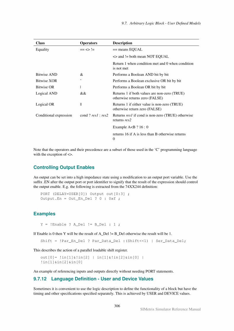
9.7. Arbitrary Logic Block - User Defined Models
Class Operators Description
Equality == <> != == means EQUAL
<> and != both mean NOT EQUAL
Return 1 when condition met and 0 when conditionis not met
Bitwise AND & Performs a Boolean AND bit by bit
Bitwise XOR ˆ Performs a Boolean exclusive OR bit by bit
Bitwise OR | Performs a Boolean OR bit by bit
Logical AND && Returns 1 if both values are non-zero (TRUE)otherwise returns zero (FALSE)
Logical OR || Returns 1 if either value is non-zero (TRUE)otherwise return zero (FALSE)
Conditional expression cond ? res1 : res2 Returns res1 if cond is non-zero (TRUE) otherwisereturns res2
Example A<B ? 16 : 0
returns 16 if A is less than B otherwise returns0
Note that the operators and their precedence are a subset of those used in the ‘C’ programming languagewith the exception of <>.
Controlling Output Enables
An output can be set into a high impedance state using a modification to an output port variable. Use thesuffix .EN after the output port or port identifier to signify that the result of the expression should controlthe output enable. E.g. the following is extracted from the 74XX244 definition:
PORT (DELAY=USER[0]) Output out[0:3] ;Output.En = Out_En_Del ? 0 : 0xf ;
Examples
Y = !Enable ? A_Del != B_Del : 1 ;
If Enable is 0 then Y will be the result of A_Del != B_Del otherwise the result will be 1.
Shift = !Par_En_Del ? Par_Data_Del :(Shift<<1) | Ser_Data_Del;
This describes the action of a parallel loadable shift register.
out[0]= !in[1]&!in[2] | in[1]&!in[2]&in[0] |!in[1]&in[2]&in[0]
An example of referencing inputs and outputs directly without needing PORT statements.
9.7.12 Language Definition - User and Device Values
Sometimes it is convenient to use the logic description to define the functionality of a block but have thetiming and other specifications specified separately. This is achieved by USER and DEVICE values.
306SIMetrix Simulator Reference Manual
9.7. Arbitrary Logic Block - User Defined Models
USER values are specified in the .MODEL statement while DEVICE values are specified on the device atthe netlist (or schematic device) level. The values are referenced in the logic definition in the form:
USER[index]
and
DEVICE[index]
These can replace any constant value in an expression, register qualifier or port qualifier. (Register and portqualifiers are the values in parentheses after the register/port keyword. E.g. DELAY, HOLD, SETUP etc.).
To set USER values in a .MODEL statement, assign the parameter USER. This is a vector parameter, thatis it can have any number of values and these must be enclosed in square brackets ‘[’ and ‘]’. For example:
.MODEL Counter8 d_logic_block file=counter_8.ldf+ user=[10n, 5n]
The logic definition to which this model refers - counter_8.ldf - can use USER[0] and USER[1] to refer tothe values 10n and 5n respectively.
To set DEVICE values in a netlist, the netlist entry for the device must be appended with:
: USER=[ values ]
For example:
A$U3 [clock] [Q0 Q1 Q2 Q3 Q4 Q5 Q6 Q7] Counter8 :+ USER=[10n, 5n]
The logic definition for this device can use DEVICE[0] and DEVICE[1] to access the USER values in thenetlist i.e. 10n and 5n respectively. Always remember to include the colon. This acts as a separatorbetween the device name and any parameters.
9.7.13 Diagnostics: Trace File
In order to debug models, a tracing facility is provided. If the .MODEL TRACE_FILE parameter orinstance parameter of the same name is specified, a file will be created which lists the values of all internalregisters at each time point.
The file will usually have a number of lines of the form: Roll back to <time>
For example the following is an extract from an actual trace file
5.00022e-05 2696 9 2696 05.09397e-05 2696 9 2696 05.09407e-05 2692 10 2692 0
Roll back to 5.08599e-05
5.09397e-05 2696 9 2696 05.09407e-05 2692 10 2692 05.09657e-05 2692 10 2692 0
Roll-back occurs when an analog time step is rejected but the digital simulation has already advanced pastthe new analog time. In this case the digital simulator has to back-track events. This mechanism is centralto the operation of the mixed-mode system and is explained in more detail in “Mixed-mode Simulator -How it Works” on page 308.
307SIMetrix Simulator Reference Manual
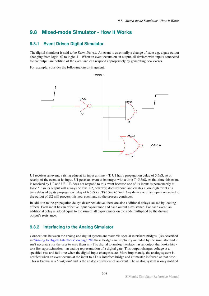
9.8. Mixed-mode Simulator - How it Works
9.8 Mixed-mode Simulator - How it Works
9.8.1 Event Driven Digital Simulator
The digital simulator is said to be Event Driven. An event is essentially a change of state e.g. a gate outputchanging from logic ‘0’ to logic ‘1’. When an event occurs on an output, all devices with inputs connectedto that output are notified of the event and can respond appropriately by generating new events.
For example, consider the following circuit fragment.
U1 receives an event, a rising edge at its input at time = T. U1 has a propagation delay of 5.5nS, so onreceipt of the event at its input, U1 posts an event at its output with a time T+5.5nS. At that time this eventis received by U2 and U3. U3 does not respond to this event because one of its inputs is permanently atlogic ‘1’ so its output will always be low. U2, however, does respond and creates a low-high event at atime delayed by its propagation delay of 6.5nS i.e. T+5.5nS+6.5nS. Any device with an input connected tothe output of U2 will process this new event and so the process continues.
In addition to the propagation delays described above, there are also additional delays caused by loadingeffects. Each input has an effective input capacitance and each output a resistance. For each event, anadditional delay is added equal to the sum of all capacitances on the node multiplied by the drivingoutput’s resistance.
9.8.2 Interfacing to the Analog Simulator
Connections between the analog and digital system are made via special interfaces bridges. (As describedin “Analog to Digital Interfaces” on page 288 these bridges are implicitly included by the simulator and itisn’t necessary for the user to wire them in.) The digital to analog interface has an output that looks like -to a first approximation - an analog representation of a digital gate. This output changes voltage at aspecified rise and fall time when the digital input changes state. More importantly, the analog system isnotified when an event occurs at the input to a D-A interface bridge and a timestep is forced at that time.This is known as a breakpoint and is the analog equivalent of an event. The analog system is only notified
308SIMetrix Simulator Reference Manual
9.9. Enhancements over XSPICE
of events that occur at the input of D-A bridges. It knows nothing of events that are internal to the digitalsystem.
Analog to digital interface bridges are much like a comparator. When the analog input passes a threshold,the output state changes appropriately and a digital event is generated.
Time Step Control
With two simulators running largely independently, something is needed to synchronise the timesteps.Basically the analog system is in control. It tells the digital system to process events up to a certain time,that time being the analog system’s next anticipated time point. A problem arises, however in that the nextanalog timestep is not guaranteed to be accepted. The analog system frequently rejects timesteps eitherbecause of slow convergence or because a shorter timestep is needed to maintain the required accuracy. Ifthe analog system has to cut back the timestep to a point prior to the most recent digital event, then thedigital system has to back-track. This process is known as roll-back and the need for the digital simulatorto be able to perform it substantially increases its complexity. In order to roll-back the digital simulator hasto store its past history back to the most recent accepted analog timepoint
9.9 Enhancements over XSPICE
• Gate delays in XSPICE are stored i.e. like a transmission line not like a real gate. SIMetrix gatedelays are inertial so if a pulse shorter than the propagation delay is received, it is swallowed nottransmitted.
• Automatic interface creation. In XSPICE you have to explicitly join digital and analog nodes viainterface bridges. In SIMetrix this is done automatically.
• Fan out implemented. The underlying mechanism for load dependent delay was there but none ofthe models supported it. Static loading effects (as in bipolar logic) was not supported at all. InSIMetrix it is.
• Input load reflected in analog to digital interfaces. The AD interfaces in XSPICE have infinite inputimpedance regardless of what the digital output is driving. SIMetrix AD interfaces reflect the digitalcapacitative and static load at their inputs.
• Output strength reflected in digital to analog interfaces. The DA interfaces in XSPICE have zerooutput impedance regardless of what is driving them. SIMetrix DA interfaces reflect the strength ofthe digital output driving the input. A hi-z logic state will look like a hi-z logic state whentransferred to the analog domain. This is not the case with XSPICE.
• AD interface threshold detection. All AD interfaces switch at a particular input threshold. In theXSPICE system the output switched at the first analog timepoint that exceeded the threshold. Thiscould be a long way passed the threshold if the analog time steps are large. In SIMetrix amechanism has been implemented that cuts back the time step so that the threshold is hit within aspecified time tolerance.
• Arbitrary logic block device. This allows the definition of any logic device using a simpledescriptive language. The language accommodates combinational logic, synchronous andasynchronous registers as well as look up tables (i.e. ROMS) and arrays (i.e. RAMs).
• Arbitrary analog to digital converter. Up to 32 bits with specified input range and offset, conversiontime and maximum conversion rate. Output may be in two’s complement or offset binary.
• Arbitrary digital to analogue converter. Up to 32 bit with specified input range and offset and outputslew time. Input may be in two’s complement or offset binary.
• Voltage controlled oscillator (analog in digital out). There was one of these in the original XSPICEcode but it suffered a number of problems and was scrapped. The SIMetrix version is all new.
309SIMetrix Simulator Reference Manual

Copyright © SIMetrix Technologies Ltd. 1992-2018
SIMetrix 8.2 Simulator Reference Manual


