Embed Size (px)
Citation preview

NASHED ET AL. VOL. XXX ’ NO. XX ’ 000–000 ’ XXXX
www.acsnano.org
A
CXXXX American Chemical Society
Self-Assembled NanostructuredPhotoanodes with Staggered Bandgapfor Efficient Solar Energy ConversionRamy Nashed,† Paul Szymanski,‡ Mostafa A. El-Sayed,‡ and Nageh K. Allam†,*
†Energy Materials Lab (EML), School of Sciences and Engineering, The American University in Cairo, New Cairo 11835, Egypt and ‡Laser Dynamics Lab (LDL),School of Chemistry and Biochemistry, Georgia Institute of Technology, Atlanta, Georgia 30332, United States
The total energy needed to power theplanet in a year is less than the sun-light energy reaching the earth in
1 h.1 Therefore, the challenge facingmodernsociety is the efficient use of the enormoussolar energy resource rather than identify-ing a sustainable energy source. Amongthe various storage protocols consideredin recent years, solar fuels2 are of particularinterest because they can be easily inte-grated with the existing fuel storage anddelivery infrastructure.Despite the significant amount of work
over the past decades to design and devel-op new functional materials for the solarfuel production,3�8 the long-standingbottleneck is to achieve an efficient chargeseparationmechanismwithout compromis-ing the bandgap. In fact, most of the pro-posed photoanodes to date suffer fromhigh charge trapping problems, which limittheir photoconversion efficiency. Towardthis end, we have recently reported a de-tailed density functional theory (DFT) studyon the Ta�W�O mixed oxide system.9 TheTa�W�O system experiences bandgap bow-ing with a highly tunable bandgap ranging
from3.7 eV for pristine Ta2O5 down to 1 eV for50% W content.9 Also, the calculationsshowed that Ta�W�O has very low holeeffective mass, comparable to that of III�Vmaterials.9
Herein, we demonstrate, for the first time,the opportunity to fabricate Ta�W�O mixedoxide nanotube arrays by a facile electro-chemical method and investigate their perfor-mance as photoanodes in photoelectro-chemical water splitting cells. The dynamicsof charge carriers were also investigated tounderstand the reasons behind the enhancedperformance of the fabricated nanotubes.
RESULTS AND DISCUSSION
Figure S1 (Supporting Information)shows the effect of anodization time, ap-plied voltage, and HF concentration on thelength, diameter, and wall thickness of theresulted nanotube arrays. Note that the wallthickness of the resulted nanotubes con-taining 10% W is smaller than their 2.5% Wcounterpart, which is expected to facilitatethe diffusion of the photogenerated hole tothe electrode/electrolyte interface, henceenhancing the water oxidation process.
* Address correspondence [email protected].
Received for review February 14, 2014and accepted April 14, 2014.
Published online10.1021/nn5009066
ABSTRACT Vertically oriented Ta�W�O nanotube array films were fabricated via the
anodization of Ta�W alloy foils in HF-containing electrolytes. HF concentration is a key
parameter in achieving well-adhered nanotube array structure. X-ray photoelectron spectroscopy
(XPS) and diffuse reflectance measurements confirm the staggered band-alignment between
Ta2O5 and WO3, which facilitates the separation of charge carriers. The nanotubes made of Ta�W
films containing 10% W showed 100-fold improvement in the measured photocurrent compared
to pristine Ta2O5 upon their use to split water photoelectrochemically. This enhancement was
related to the efficient charge transport and the red shift in absorption spectrum with increase of
the W content, which was asserted by ultrafast transient absorption (TA) spectroscopy
measurements. The TA measurements showed the elimination of trap states upon annealing Ta�W�O nanotubes and, hence, minimizing the charge
carrier trapping, whereas the trap states remain in pristine Ta2O5 nanotubes even after annealing.
KEYWORDS: Ta�W�O . staggered bandgap . solar . transient absorption . laser dynamics
ARTIC
LE
NASHED ET AL. VOL. XXX ’ NO. XX ’ 000–000 ’ XXXX
www.acsnano.org
B
Note also that the anodization time has more pro-nounced effect on the 10% W alloy compared to the2.5%W-containing alloy. For example, upon increasingthe anodization time from 15 to 35 min, the nanotubelength increases from 0.84 to 1.2 μm for the 2.5% Walloy, whereas it changes from1.2 to 6.4 μmfor the 10%W alloy. Increasing the anodization potential resultedin an increase in the nanotube length and diameter forboth 2.5% and 10%Walloys, with a higher effect on the10% W alloy (Figure S1c,d). The nanotube wall thick-ness increases from 9 to 20.5 nm for the 2.5% W alloy,whereas it nearly remains constant at around 10.5 nmfor the 10% W alloy as the anodization potentialincreases from 10 to 20 V. Although the nanotubelength for the 2.5% W alloy does not seem to beaffected by the anodization time and applied potential,it is influenced by the HF concentration, where thenanotube length increases from 0.6 to 3.2 μm as theHF concentration increases from 0.51 to 0.85 M thenit decreases to 1.2 μm at 1.17 M HF (Figure S1e).The nanotube diameter and wall thickness show thesame dependence on HF concentration. Figure S2 inthe Supporting Information shows the SEM images forthe resulted nanotubes at different conditions.Although we were able to fabricate nanotubes with
controlled length, diameter, and wall thickness, theydo not adhere well to the substrate upon their anneal-ing, due to the formation of TaF5 layer between theoxide layer and the alloy substrate.10,11 In an attempt tolimit the formation of the TaF5 barrier layer, the anodi-zation was done in relatively short times. The anodiza-tion of Ta and Ta�W foils in an electrolyte containing2.9 M HF and 16.4 M H2SO4 at 15 V resulted in theformation of well-adhered nanotube layers. It is
noteworthy that for pure Ta and 2.5%W alloy, we wereable to fabricate nanotubes after 20 s only, whereas atleast 2 min of anodization were needed for theTa�10% W alloy in order to obtain nanotubular struc-ture. This is probably due to the formed WO3, whichhas different reactivity toward F� ions compared toTa2O5. This is asserted by the fact that the maximumobtained nanotube length decreases progressivelyfrom 3.3 μm for pure Ta2O5 to 2.1 μm for 2.5% W, to1.4 μm for 10% W, with increasing the amount of W.Figure 1 shows the SEM images of the obtainednanotubes.The fabricated nanotubes have an orthorhombic
crystal structure with estimated volume expansionsof 2.9% and 3.8% for the samples containing 2.5% Wand 10% W, respectively compared to pristine Ta2O5.
9
Figure 2 shows the XRD pattern for pristine andTa�W�O mixed oxide nanotubes that have been an-nealed at 450 �C for different annealing times. Generally,the peaks are shifted toward higher 2θ values as theannealing time increases, indicating a contraction in thecrystal lattice. This is because heating the lattice forlonger times allows theatoms to readjust their positions,minimizing the total energy of the system. The trend isnot the same for the samples containing 10%W, wheremainly intensity fluctuations and a slight shift to lower2θ values occurred upon annealing. These samplesappear to have phase separation with increased split-tingof thehigher 2θpeaks relative to the correspondingpeaks of the 2.5% W-containing samples. Also, theextent of peak shifting decreases as the W contentincreases, which can be attributed to the fact that Watom has larger size than Ta atom, allowing less spacefor the atoms to move in the lattice, in turn decreasing
Figure 1. FESEM images of the films resulted upon the anodization of (a) pure Ta, (b) Ta�2.5%W, and (c) Ta�10%W foils at15 V in 16.4 M H2SO4 and 2.9 M HF electrolytes for 3 min.
ARTIC
LE

NASHED ET AL. VOL. XXX ’ NO. XX ’ 000–000 ’ XXXX
www.acsnano.org
C
the extent of freedom for readjustment. Note that thepeak shoulder at 2θ = 53� (plane (331) inWO3) indicatesthe presence of a small precipitation of WO3-rich phaseleading to amicroscale heterojunction. This helps in thecharge separation, which in turn is expected to result ina higher electric current, since Ta2O5�WO3 heterojunc-tion was found to have a staggered bandgap.9 Figure 3illustrates the staggeredbandgapalignment in Ta�W�Oalloy. Upon illumination, the electrons are excited fromthe valence band of Ta2O5 to the conduction band ofWO3. Electrons have a potential barrier toward the Ta2O5
side, which forces them to flow rightward, whereas holeshave a potential barrier toward the WO3 side forcingthem to flow leftward, and hence an efficient chargeseparation is achieved.9 On the other hand, straddled
band alignment (such as that present in Ti�Fe�Osystem) gives rise to electron trapping in the conductionband, as shown in Figure 3b, and, in turn, reduces theconversion efficiency.9,12 We believe that this is the mainreason behind the modest efficiency reported so far forphotoelectrochemical water splitting systems based onstraddled band alignment.To study the composition of the fabricated Ta2O5
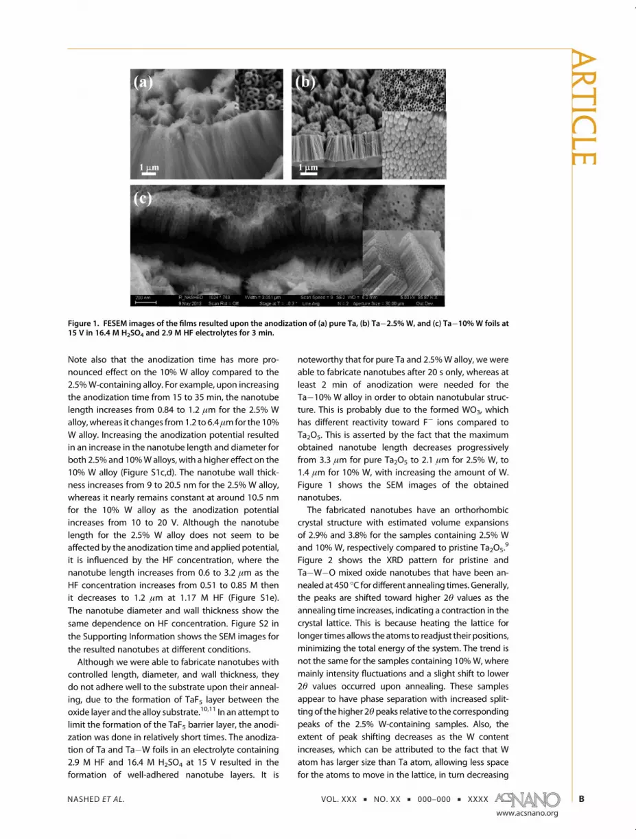
and Ta�W�Onanotubes, XPS analysis was performed,Figure 4. The O 1s peak was observed between 530.5and 530.9 eV, in agreement with the O 1s peak reportedfor Ta2O5 andWO3.
13�16 In pure Ta2O5, Ta 4f peaks existat 26.3 and 28.1 eV corresponding to 4f7/2 and 4f5/2peaks, respectively, with a separation of 1.8 eV, indicat-ing the existence of Ta5þ.17 As the W content increases
Figure 2. XRD pattern for the annealed (a�c) pristine, (d�f) Ta�2.5% W�O, and (g�i) Ta�10% W�O nanotube samples.
Figure 3. Energy band diagrams of (a) Ta�W�O and (b) Ti�Fe�O, showing the charge carrier transport for both systems,thus illustrating the efficient charge separation in Ta�W�O alloy.
ARTIC
LE
NASHED ET AL. VOL. XXX ’ NO. XX ’ 000–000 ’ XXXX
www.acsnano.org
D
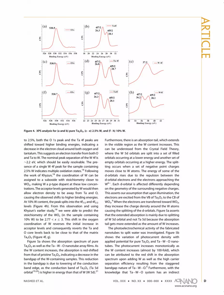
to 2.5%, both the O 1s peak and the Ta 4f peaks areshifted toward higher binding energies, indicating adecrease in the electron cloud around both oxygen andtantalum. This suggests an electron transfer frombothOand Ta toW. The nominal peak separation of theW 4f is∼2.2 eV, which should be easily resolvable. The pre-sence of a single W 4f peak for the sample containing2.5% W indicates multiple oxidation states.18 Followingthe work of Khyzun,18 the coordination of W can beassigned to a suboxide with stoichiometry closer toWO2, making W a p-type dopant at these low concen-trations. The acceptor levels generatedbyWwould thenallow electron density to be away from Ta and O,causing the observed shifts to higher binding energies.At 10%W content, the peak splits into the 4f7/2 and 4f5/2levels (Figure 4h). From this observation and usingKhyzun's earlier study,18 we were able to predict thestoichiometry of the WOx (in the sample containing10% W) to be 2.77 < x e 3. This shift in the oxygencoordination of W reverses the initial increase inacceptor levels and consequently reverts the Ta andO core levels back to be close to that of the matrixTa2O5 (Figure 4f, g).Figure 5a shows the absorption spectrum of pure
Ta2O5 as well as the Ta�W�O nanotube array films. Asthe W content increases, the absorption is red-shiftedfrom that of pristine Ta2O5, indicating a decrease in thebandgap of the W-containing samples. This reductionin the bandgap is due to lowering of the conductionband edge, as the conduction band of Ta2O5 (Ta 5dorbital19,20) is higher in energy than that of W (W 5d).21
Furthermore, there is an absorption tail, which extendsin the visible region as the W content increases. Thiscan be understood from the Crystal Field Theory,where the W 5d orbitals are split into a set of filledorbitals occurring at a lower energy and another set ofempty orbitals occurring at a higher energy. The split-ting occurs when a set of negative point chargesmoves close to W atoms. The energy of some of thed-orbitals rises due to the repulsion between thed-orbital electrons and the electrons approaching theW6þ. Each d-orbital is affected differently dependingon the geometry of the surrounding negative charges.This asserts our assumption that upon illumination, theelectrons are excited from the VB of Ta2O5 to the CB ofWO3.
9 When the electrons are transferred towardWO3,they increase the charge density around the W atomscausing the splitting of the d-orbitals. Figure 5a assertsthat the extended absorption is mainly due to splittingof W 5d orbital and not Ta 5d because the absorptiontail gets more extended as the amount of W increases.The photoelectrochemical activity of the fabricated
nanotubes to split water was investigated. Figure 5bshows the variation of photocurrent density withapplied potential for pure Ta2O5 and Ta�W�O nano-tubes. The photocurrent increases monotonically asthe W content increases (almost by 100-fold), whichcan be attributed to the red shift in the absorptionspectrum upon adding W as well as the high carrierseparation efficiency resulting from the staggeredbandgap nature of Ta�W�O.9 Furthermore, with theknowledge that Ta�W�O system has an indirect
Figure 4. XPS analysis for (a and b) pure Ta2O5, (c�e) 2.5% W, and (f�h) 10% W.
ARTIC
LE
NASHED ET AL. VOL. XXX ’ NO. XX ’ 000–000 ’ XXXX
www.acsnano.org
E
bandgap,9 the length of the nanotubes is a significantfactor in improving photon absorption, as indirectbandgap materials have low absorption coefficientscompared to their direct bandgap counterparts,22 andhence, the optical path of light needs to be increased inorder to increase the probability of photon absorption.This is asserted in Figure 5b where the photocurrentincreases by more than five times with increasing thenanotube length in the sample containing 10%W from0.5 to 1.4 μm. Moreover, the onset potential is shiftedtoward more negative values as the W content in-creases. This is because as theW content increases, thedonor energy level is shifted more toward the conduc-tion band edge, which in turn, shifts the Fermi leveltoward more negative potential. This is a desirableproperty since this open circuit potential representsthe contribution of light toward the minimum poten-tial difference required for water splitting (1.23 V).2
Table S1 summarizes the obtained onset potentials aswell as the maximum photocurrent density for Ta2O5
and Ta�W�O nanotubes.Transient absorption (TA) spectroscopy was shown
to be a very efficient technique to investigate thecharge carrier dynamics in semiconductor films.23�29
In fact, TA spectroscopy is playing a vital role in theadvancement of dye-sensitized solar cells by providinga very deep understanding on charge carriers separa-tion, transport, and recombination, which, in turn,allows for overcoming the deficiencies in the deviceperformance and hence help designing more efficientsystems for energy conversion.27�29 Unfortunately, theanalogous process in photoelectrochemical conver-sion (PEC) is not yet understood to the same level ofdetails as the solar cell counterpart. Therefore, a lotmore work is still needed in this field to achieveadequately efficient PEC systems.30
The TA spectra (Figures 6 and 7) and dynamics(Figure8)werecollected for the longestnanotubesamplesof each doping level at a pump energy of 800 nJ/pulse,the lowest energy where a measurable signal couldbe obtained for every sample. A Helios UV�visible
spectrometer (Ultrafast Systems) was used for themeasurements. Two different pumpwavelengths wereused to compare UV (340 nm) with visible (490 nm)excitation. Pump light at 340 nm was obtained fromthe fourth harmonic of the signal from a CoherentOPerA Solo optical parametric amplifier, which waspumped by a Coherent Libra regeneratively amplifiedTi:sapphire laser (809 nm, 50 fs pulses, 1 kHz repetitionrate). The sum frequency of the signal and the laserfundamental wavelength was used to produce pumplight at 490 nm. A broadband probe beam was pro-duced by focusing a small fraction of the fundamentalwavelength into a sapphire crystal. Both pump andprobe were focused and overlapped on the surface ofthe substrate, with the pump spot diameter∼1mm. Asthe metal substrates do not transmit light, reflectedprobe light is used to determine the transient absorp-tion by focusing it into a fiber-coupled Si array detectorwith a detection range of 300�907 nm. Typically, onlyprobe light at 700 nmand above could be collected in areasonable amount. A chopper blocks every other pumppulse with the difference between two consecutivespectra, one with the pump beam and one without,yielding the TA signal ΔA(t), where t is the time delaybetween pump and probe pulses.TA signals collected from clean, anodized metal
substrates reflect contributions from metal-oxidenanotubes, a thin oxide barrier layer at the substratesurface, and transient reflectivity of the substrate. Toisolatenanotubecontributions toTA,measurementswerealso performed on clean, unanodized substrates underthe handling conditions (unannealed versus annealed)and using the same pump wavelengths. Substratesignals were then scaled as follows. Transient absorp-tion signals for each anodized sample were summedover all probe wavelengths 700�907 nm, where in-duced absorption (ΔA> 0) was observed, ignoringwave-lengths with negative ΔA as no steady-state absor-bance was seen at these wavelengths (Figure 6a).Signals from the corresponding unanodized substrateswere summed over the same wavelengths. Dynamics
Figure 5. (a) Diffuse reflectance spectra (DRS) for pure Ta2O5 and Ta�W�O nanotube electrodes annealed at 450 �C for 9 h inair; (b) photocurrent density versus potential in 1 M KOH solution under AM1.5 illumination for pure Ta2O5 and Ta�W�Onanotubes.
ARTIC
LE

NASHED ET AL. VOL. XXX ’ NO. XX ’ 000–000 ’ XXXX
www.acsnano.org
F
from each nanotube-containing sample were thenfitted using
ΔA(t) ¼ a1e�t=τ1 þ a2e
�t=τ2 þ asΔAs(t)þ c (1)
whereΔAs(t) is the signal from the substrate alone, as isa positive scaling factor for the substrate signal, a1 anda2 are amplitudes of exponential decays with corre-sponding time constants τ1 and τ2, and c is a constant
offset. The average decay lifetime of the nanotubesignal over an observation window of ∼3 ns is thencalculated as
Æτæ ¼ a1τ1 þ a2τ2a1 þ a2
(2)
Values for fitting parameters are given in Table 1.Figure 7 shows TA spectra measured using UV
(340 nm) excitation, with substrate signals scaled by
Figure 7. Visible (490 nm) pump TA spectra at 1 ps pump�probe delay for nanotubes made from Ta alloys with Wcompositions of 2.5% (red, top row) and 10% (green, bottom row). Both unannealed (left column) and annealed (rightcolumn) nanotubes are shown. Dotted lines show transient spectra from clean, unanodized substrate under the sameconditions (TA pump wavelength and annealing).
Figure 6. UV (340 nm) pump TA spectra at 1 ps pump�probe delay for nanotubesmade from Ta alloys withW compositionsof 0% (black, top row), 2.5% (red, middle row), and 10% (green, bottom row). Both unannealed (left column) and annealed(right column) nanotubes are shown. Dotted lines show transient spectra from clean, unanodized substrate under the sameconditions (TA pump wavelength and annealing).
ARTIC
LE

NASHED ET AL. VOL. XXX ’ NO. XX ’ 000–000 ’ XXXX
www.acsnano.org
G
as. Spectra for doped samples excited with visible(490 nm) light are shown in Figure 8, with the pumplight exciting W-doped Ta2O5 domains exhibiting alower band gap. The spectra are shown at a pump�probe delay of 1 ps; analogous spectra at negativedelays (probe arriving 1 ps before pump) are shown inFigures S3 and S4. In the red-to-near-IR region(700�907 nm), the nanotubes show positive ΔA con-sistent with absorption by initially unoccupied states
within the band gap, which we interpret as trappedelectrons below the conduction-band edge similar toother metal oxides such as TiO2,
23 Fe2O3,24 and
ZnO.25,26 A comparison with spectra acquired at nega-tive delays (Figures S3 and S4) rules out experimentalartifacts as the dominant origin of this signal. Unan-nealed samples show significant densities of defectstates, especially for 10% W alloy nanotubes. Notethat the increased defect absorbance exists despite
Figure 8. Transient absorption dynamics from nanotubes made by anodizing Ta alloy with 10% W content. Pump energy is800 nJ/pulse, and signals are summed over probewavelengths 700�907 nmwhere induced absorption (ΔA > 0) is observed.(a) Unannealed sample, 340 nm pump; (b) unannealed sample, 490 nm pump; (c) annealed sample, 340 nm pump; (d)annealed sample, 490 nm pump. Background signals are measured from clean, unanodized substrates under the sameconditions (pump wavelength and annealing), multiplied by a scaling factor, and incorporated into fits of the dynamics (seetext). For (d), no fit is shown as the nanotubes do not show induced absorption except for a positive spike at zero delay.
TABLE 1. Carrier Lifetimes as a Function of Composition and Pump Wavelength
% W annealing pump wavelength (nm) a1 (mOD) τ1 (ps) a2 (mOD) τ2 (ps) Æτæ (ps) as
0 No 340 180 (50) 230 (40) 230 (40) 2.4 (0.1)0 Yes 340 147 (6) 20 (2) 20 (2) 0.06 (0.07)2.5 No 340 60 (10) 9 (3) 9 (3) 1.09 (0.01)2.5 No 490 140 (40) 100 (30) 100 (30) 0.4 (0.1)2.5 Yes 340 12.3 (0.8) 16 (2) 16 (2) 0 (0.01)2.5 Yes 490 No signal from nanotubes10 No 340 240 (60) 6 (1) 150 (50) 300 (200) 130 (30) 0.4 (0.4)10 No 490 150 (60) 25 (6) 150 (40) 400 (100) 220 (50) 0.5 (0.4)10 Yes 340 52.0 (0.8) 120 (60) 120 (60) 0.2 (0.1)10 Yes 490 No signal from nanotubes
a Values in parentheses are uncertainties in the fits. mOD = millioptical density units.
ARTIC
LE

NASHED ET AL. VOL. XXX ’ NO. XX ’ 000–000 ’ XXXX
www.acsnano.org
H
the decrease in the nanotube length with doping. Forannealed samples, the absorption by defects ap-proaches zero in doped samples. This is consistent withthe fact that annealing improves the metal-oxide latticecrystallinity, therefore decreasing the defect density.Although the experiment does not yield an exact den-sity of trapped carriers, the reduction in absorbancedoes reflect decreases in the number of trapped carriersdue to annealing. Note that the defect density remainssignificant in pure Ta2O5 nanotubes even after anneal-ing (Figure 7). Note also that charge trapping is identi-fied as the most significant limiting factor in designingefficient photoanodes in PEC systems.31 Eliminating trapstates should minimize the charge trapping and henceimprove the photocurrent. This can be considered themain reason behind the observed enhancement of thephotocurrent for the Ta�W�O photoanodes, besidesthe red shift in the absorption spectrumand theefficientcharge separation due to the staggered band alignmentbetween Ta2O5 and WO3.
9
Figure 8 and Figures S5 and S6 (see SupportingInformation) depict the TA dynamics for the differentfabricated samples from which the carrier lifetimes areextracted according to eqs 1 and 2. Table 1 summarizesthe lifetimes at two pump wavelengths, namely 340and 490 nm. It can be inferred that the 340 nm signal iscapable of exciting the electrons from the VB to the CBof Ta�W�O system. On the other hand, the 490 nmcan excite the electrons into trap states within thebandgap. Table 1 shows that at the low pumping wave-length (340 nm), the lifetimes for 2.5%W and 10%W arevery close for both unannealed and annealed samples(9 vs 16 ps for unannealed and annealed 2.5%W, respec-tively, and130 versus120ps for unannealedandannealed2.5% W and 10% W, respectively). The close lifetimestogether with the low pumping wavelength assert thatthese lifetimes can be attributed to thermalization pro-cesses, especially that thermalization is affected by theband structure of the material and not its crystallinity.Furthermore, the lifetime at 340 nm for 2.5%W is muchless than its 10% W counterpart suggesting a denserband structure in case of 2.5% W compared to the10% W case,24 in agreement with our previous study.9
As a final remark, it might be argued that shallowdefect states might assist the promotion of the photo-generatedelectrons to the conductionbandbyprovidinga transit state to the electrons generatedby sub-bandgapphotons. However, it was found that conduction-bandelectron lifetimes in TiO2 devices are in the millisecondrange as observed in dye-sensitized solar cells, 9 orders ofmagnitude slower than the lifetime in trap states, andthus, it is extremely unlikely that electrons in Ta or Ta�Woxide nanotube defect states can contribute to current ina PEC system. The effects of annealing in reducing defectdensity should improve the conductivity of the nano-tubes. The TA results are thus consistent with the greatlyenhanced photocurrent produced by the nanotubescontaining 10% W (Figure 5b).
CONCLUSION
In summary, vertically oriented Ta�W�O nanotubearray filmswere fabricated via a simple electrochemicalanodization of Ta�W ally foils. The nanotube length,diameter, and thickness were found to depend on theanodization conditions, with the foil containing 10%Wshowing more sensitivity to anodization conditions.Increasing the W content resulted in an increase in thenanotube length due to the increased stresses in thecrystal lattice upon incorporation of W atoms. XRDanalysis showed an expansion of 2.9% and 3.8% in thecrystal lattice upon the addition of 2.5% and 10% W,respectively. The extent of expansion decreases withincreasing the annealing time. XPS analysis illustratesthat charge transfer occurs from Ta and O atoms to Watoms, as confirmed by the tail in the absorption spectraof Ta�W�O nanotubes. Finally, the photocurrent of thenanotubes made of Ta�W films containing 10% W wasincreased by about 10-fold compared to pristine Ta2O5
owing to efficient charge carriers separation due to thestaggered band alignment between Ta2O5 andWO3 andthe red shift of the absorption spectrum. Ultrafast tran-sient absorption spectroscopy illustrates the eliminationof trap states upon annealing Ta�W�O nanotubes,hence minimizing the charge carrier trapping, leadingto a large photocurrent, whereas the trap states exist inpristine Ta2O5 nanotubes even after annealing.
MATERIALS AND METHODSPrior to anodization, pure Ta samples as well as 2.5% and 10%
W Ta�W alloys (Goodfellow, USA) were cleaned in acetone for30 min followed by 30 min in deionized water in an ultrasonicbath. A two-electrode electrochemical cell was used for anodi-zation with Ta and Ta�W samples as the working electrode andPt foil as the counter electrode. For the nonadhering nanotubes,the anodization was carried out in a solution of concentratedsulfuric acid (95�98%) and HF (48%) where the sulfuric acidmolarity was kept at 16.4 M and HF molarity was swept from0.51 to 1.17 M. The anodization voltage was varied between10 and 25 V, and the anodization time was varied between 5 to35 min. For the well-adhered nanotubes, the same H2SO4/HF
solution was used with a volumetric ratio of 9:1. The solutionwas magnetically stirred during anodization at a speed of60 rpm and kept at room temperature where the electrodeseparation was approximately 1 cm. The anodization voltagewas kept at 14.5 V, and the anodization time varied between2 and 4 min. After anodization, the as-anodized samples wereannealed in an air atmosphere for 4 or 9 h at 450 �C at a rate of1 �C/min for both heating and cooling.A Zeiss SEM Ultra 60 field emission scanning electron micro-
scope (FESEM) with an In-Lens detector was used to study themorphology of the samples at a voltage between 5 and 10 kV.A Thermo Scientific K-alpha XPS spectrometer with an Alanode was used for the XPS measurements, with the spectra
ARTIC
LE
NASHED ET AL. VOL. XXX ’ NO. XX ’ 000–000 ’ XXXX
www.acsnano.org
I
charge-referenced toO 1s at 532 eV. The crystalline phasesweredetected and identified using Alpha-1 Panalytical XRD instru-ment with a Cu KR radiation at λ = 1.540598 Å at a scan step (2θ)of 0.004�. A Shimadzu UV-3101PC UV-Vis-NIR spectropho-tometer was used for the optical characterization of the films.The photoelectrochemical measurements were performed in athree-electrode electrochemical cell. In this configuration, thenanotube films were used as photoanodes, platinum foil as thecounter electrode, and saturated Ag/AgCl as the referenceelectrode, immersed in 1.0 M KOH. The dark and illuminatedcurrents were monitored using a scanning potentiostat(CH Instruments, CHI 760) at a scan rate of 10 mV/s. A 300 Wozone-free xenon lamp equipped with AM 1.5G filter was usedto simulate sunlight at 100 mW/cm2.
Conflict of Interest: The authors declare no competingfinancial interest.
Supporting Information Available: Additional SEM images,onset potential table as a function of W content and nanotubelength, additional carrier dynamics figures. This material isavailable free of charge via the Internet at http://pubs.acs.org.
Acknowledgment. M.A.E. would like to acknowledge thefinancial support by the U.S. Department of Energy, Office ofBasic Energy Sciences, Grant No. DE-FG02-97-ER-14799 andN.K.A. would like to acknowledge the support by The AmericanUniversity in Cairo, Grant No. SS-PHY-RII 013-R7.
REFERENCES AND NOTES1. Lewis, N. S. Powering the Planet.MRSBull.2007, 32, 808–820.2. Grimes, C. A.; Varghese, O. K.; Ranjan, S. Light, Water,
Hydrogen: The Solar Generation of Hydrogen by WaterPhotoelectrolysis; Springer: New York, 2008.
3. Allam, N. K.; Poncheri, A. J.; El-Sayed, M. A. VerticallyOriented Ti-Pd Mixed Oxynitride Nanotube Arrays forEnhanced Photoelectrochemical Water Splitting. ACSNano 2011, 5, 5056–5066.
4. Mor, G. K.; Prakasam,H.E.; Varghese,O. K.; Shankar, K.;Grimes,C. A. Vertically Oriented Ti-Fe-O Nanotube Array Films:Toward a Useful Material Architecture for Solar SpectrumWater Photoelectrolysis. Nano Lett. 2007, 7, 2356–2364.
5. Allam, N. K.; Alamgir, F.; El-Sayed, M. A. Enhanced Photo-assisted Water Electrolysis Using Vertically Oriented Ano-dically Fabricated Ti�Nb�Zr�O Mixed Oxide NanotubeArrays. ACS Nano 2010, 4, 5819–5826.
6. Ko, J. W.; Ryu, W.-H.; Kim, I.-D.; Park, C. B. Bi-FunctionalRuO2-Co3O4 Core-Shell Nanofibers as a Multi-ComponentOne-Dimensional Water Oxidation Catalyst. Chem. Com-mun. 2013, 49, 9725–9727.
7. Allam, N. K.; Deyab, N. M.; Abdel Ghany, N. Ternary Ti-Mo-Ni Mixed OxideNanotube Arrays as Photoanode Materialsfor Efficient Solar Hydrogen Production. Phys. Chem.Chem. Phys. 2013, 15, 12274–12282.
8. Allam, N. K.; Shaheen, B. S.; Hafez, A. M. Layered TantalumOxynitride Nanorod Array Carpets for Efficient Photoelec-trochemical Conversion of Solar Energy: Experimental andDFT Insights. ACS Appl. Mater. Interfaces 2014, 6, 4609–4615.
9. Nashed, R.; Alamgir, F. M.; Jang, S. S.; Ismail, Y.; El-Sayed,M. A.; Allam, N. K. Bandgap Bowing in Ta-W-O System forEfficient Solar Energy Conversion: Insights from Density-Functional Theory and X-Ray Diffraction. Appl. Phys. Lett.2013, 103, 133905.
10. Shimizu, K.; Kobayashi, K.; Thompson, G. E.; Skeldon, P.;Wood, G. C. The Migration of Fluoride Ions in GrowingAnodic Oxide Films on Tantalum. J. Electrochem. Soc.1997, 144, 418–423.
11. Allam, N. K.; Feng, X. J.; Grimes, C. A. Self-AssembledFabrication of Vertically Oriented Ta2O5 Nanotube Arrays,and Membranes Thereof, by One-Step Tantalum Anodiza-tion. Chem. Mater. 2008, 20, 6477–6481.
12. Nashed, R.; Alamgir, F. M.; Jang, S. S.; Ismail, Y.; El-Sayed,M. A.; Allam, N. K. Towards a Perfect System for SolarHydrogen Production: An Example of Synergy on theAtomic Scale. Proc. SPIEE 2013, 8822, No. 88220A .
13. Ho, S. F.; Contarini, S.; Rabalais, J. W. Ion-Beam-InducedChemical Changes in the Oxyanions (Moyn-) and Oxides(Mox) where M = Chromium, Molybdenum,Tungsten,Vanadium, Niobium and Tantalum. J. Phys. Chem. 1987,91, 4779–4788.
14. Thomas, J. H.; Hammer, L. H. A Photoelectron SpectroscopyStudy of CF4/H2 Reactive Ion Etching Residue on TantalumDisilicide. J. Electrochem. Soc. 1989, 136, 2004–2010.
15. Colton, R. J.; Guzman, A. M.; Rabalais, J. W. Electrochro-mism in Some Thin-Film Transition-Metal Oxides Charac-terized by X-RayElectron Spectroscopy. J. Appl. Phys. 1978,49, 409–416.
16. Kerkhof, F. P. J. M.; Moulijn, J. A.; Heeres, A. The XPS Spectraof the Metathesis Catalyst Tungsten Oxide on Silica Gel.J. Electron Spectrosc. Relat. Phenom. 1978, 14, 453–466.
17. Kurnia, F.; Hadiyawarman; Jung, C. U.; Jung, R.; Liu, C.Composition Dependence of Unipolar Resistance Switch-ing in TaOx Thin Films. Phys. Status Solidi 2011, 5, 253–255.
18. Khyzhun, O. Y. XPS, XES and XAS Studies of the ElectronicStructure of Tungsten Oxides. J. Alloys Compd. 2000, 305,1–6.
19. Nashed, R.; Hassan, W. M. I.; Ismail, Y.; Allam, N. K. Unravel-ling the Interplay of Crystal Structure and Electronic BandStructure of Tantalum Oxide (Ta2O5). Phys. Chem. Chem.Phys. 2013, 15, 1352–1357.
20. Wu, Y.-N.; Li, L.; Cheng, H.-P. First-Principles Studies ofTa2O5 Polymorphs. Phys. Rev. B 2011, 83, 144105.
21. Nozik, A. J. Photoelectrochemistry: Applications to SolarEnergyConversion.Annu. Rev. Phys. Chem.1978,29, 189–222.
22. Yacobi, B. G. Semiconductor Materials: An Introduction toBasic Principles; Kluwer Academic/PlenumPublishers: NewYork, 2003.
23. Tamaki, Y.; Hara, K.; Katoh, R.; Tachiya, M.; Furube, A.Femtosecond Visible-to-IR Spectroscopy of TiO2Nanocrys-talline Films: Elucidation of the Electron Mobility beforeDeep Trapping. J. Phys. Chem. C 2009, 113, 11741–11746.
24. Wheeler, D. A.; Wang, G. M.; Ling, Y. C.; Li, Y.; Zhang, J. Z.Nanostructured Hematite: Synthesis, Characterization,Charge Carrier Dynamics, and Photoelectrochemical Prop-erties. Energy Environ. Sci. 2012, 5, 6682–6702.
25. Li, M. J.; Xing, G. C.; Xing, G. Z.; Wu, B.; Wu, T.; Zhang, X. H.;Sum, T. C. Origin of Green Emission and Charge TrappingDynamics in ZnONanowires. Phys. Rev. B2013, 87, 115309.
26. Bauer, C.; Boschloo, G.; Mukhtar, E.; Hagfeldt, A. UltrafastRelaxation Dynamics of Charge Carriers Relaxation in ZnONanocrystalline Thin Films. Chem. Phys. Lett. 2004, 387,176–181.
27. Planells, M.; Pelleja, L.; Clifford, J. N.; Pastore, M.; De Angelis,F.; Lopez, N.; Marder, S. R.; Palomares, E. Energy Levels,Charge Injection, Charge Recombination and Dye Regen-eration Dynamics for Donor-Acceptor pi-ConjugatedOrganic Dyes in Mesoscopic TiO2 Sensitized Solar Cells.Energy Environ. Sci. 2011, 4, 1820–1829.
28. Mohammadpour, R.; Zad, A. I.; Hagfeldt, A.; Boschloo, G.Comparison of Trap-State Distribution and Carrier Trans-port in Nanotubular and Nanoparticulate TiO2 Electrodesfor Dye-Sensitized Solar Cells. ChemPhysChem 2010, 11,2140–2145.
29. Listorti, A.; O'Regan, B.; Durrant, J. R. Electron TransferDynamics in Dye-Sensitized Solar Cells. Chem. Mater.2011, 23, 3381–3399.
30. Pendlebury, S. R.; Barroso, M.; Cowan, A. J.; Sivula, K.; Tang,J.; Graetzel, M.; Klug, D.; Durrant, J. R. Dynamics of Photo-generated Holes in Nanocrystalline Alpha-Fe2O3 Electro-des for Water Oxidation Probed by Transient AbsorptionSpectroscopy. Chem. Commun. 2011, 47, 716–718.
31. Tang, J. W.; Durrant, J. R.; Klug, D. R. Mechanism ofPhotocatalytic Water Splitting in TiO2. Reaction of Waterwith Photoholes, Importance of Charge Carrier Dynamics,and Evidence for Four-Hole Chemistry. J. Am. Chem. Soc.2008, 130, 13885–13891.
ARTIC
LE