Embed Size (px)
Citation preview
SATHYABAMA INSTITUTE OF SCIENCE AND TECHNOLOGY SCHOOL OF BUILDING AND
ENVIRONMENT
SECA1601 MICROPROCESSORS AND MICROCONTROLLERS L T P Credits Total Marks
3 0 0 3 100
COURSE OBJECTIVES
To understand the architecture of Microprocessor & Microcontroller. To familiarize the students in writing assembly programming and interfacing with peripherals. To provide foundation and confidence to the students to solve real world problem using Microprocessor and
Microcontroller.
UNIT 1 INTRODUCTION TO MICROPROCESSORS 9 Hrs. Introduction, 8085 Architecture, Pin Diagram and signals, Timing Diagram, Interrupts and its types, Introduction to
8086 microprocessors and its operation
UNIT 2 PROGRAMMING 8085 MICROPROCESSOR 9 Hrs. 8085 assembly language programming- addressing modes, Instruction formats, Instruction Classification- data transfer,
arithmetic operations, logical operations, branching operations, I/O and machine control —Stack and subroutines, Example
Programs
UNIT 3 PERIPHERALS AND INTERFACING 9 Hrs. Introduction, Serial communication USART (8251), Programmable Peripheral Interface (8255), Programmable Interrupt
Controller (8259), Programmable interval timer (8254),DMA controller(8257), Analog to Digital Converter (ADC), and
Digital to Analog Converter (DAC).
UNIT 4 8051 MICROCONTROLLER 9 Hrs. Introduction to microcontrollers, Difference between microprocessor and microcontroller, Architectural of 8051, Memory architecture, Timers, Interrupts, Addressing Modes and Instruction set of 8051, Programming examples.
UNIT 5 APPLICATIONS BASED ON 8085 AND 8051 9 Hrs. Interfacing LED, 7 segment LED Display, Stepper motor control system, Temperature control system, Motor speed control system, Timer application program, Interfacing LCD.
Max. 45 Hrs
COURSE OUTCOMES On completion of the course, student will be able to CO1 - Understand the architecture and operations of various functional block of 8085 CO2 - Write assembly language program by understanding addressing modes and the various instructions
CO3 - Identify the need for various interfacing ICs and explain it’s function
CO4 - Understand the architecture and function of various on chip modules of 8051 Microcontroller CO5 - Understand the addressing modes of 8051 and write programs
CO6 - Design and develop program for various I/O units and for real world problem
TEXT / REFERENCE BOOKS 1. Ramesh Gaonkar, "Microprocessor Architecture, Programming and applications with 8085", 6/e, Penram International
Publishing Pvt. Ltd., 2013. 2. Kenneth J Ayala, "The 8051 Microcontroller", 3rd Edition, Thomson, 2007. 3. Muhammad Ali Mazidi, "The 8051 Microcontroller and Embedded Systems", 2nd Edition, Pearson Education, 2013. 4. K.M.Bhurchandi and A.K.Ray, "Advanced Microprocessors and Peripherals", Tata McGraw Hill Education Private
Limited, 3rd Edition, 2013.
5. https://www.mikroe.com/ebooks/architecture-and-programming-of-8051-mcus/introduction.
END SEMESTER EXAMINATION QUESTION PAPER PATTERN
Max. Marks: 100 Exam Duration: 3 Hrs.
PART A: 10 Questions of 2 marks each – No choice 20 Marks PART B: 2 Questions from each unit of internal choice; each carrying 16 marks 80 Marks
B.E. / B.Tech. - Part Time 26 REGULATIONS
2019
1
UNIT – I – MICROPROCESSORS AND MICROCONTROLLERS– SECA 1601
SCHOOL OF ELECTRICAL AND ELECTRONICS
DEPARTMENT OF ELECTRONICS AND COMMUNICATION ENGINEERING
2
UNIT 1 INTRODUCTION TO MICROPROCESSORS
Introduction, 8085 Architecture, Pin Diagram and signals, Addressing Modes, Timing
Diagram, Memory read, Memory write, I/O cycle, Interrupts and its types, Introduction
to 8086 microprocessors and its operation.
History of microprocessor:
The invention of the transistor in 1947 was a significant development in the world of
technology. It could perform the function of a large component used in a computer in
the early years. Shockley, Brattain and Bardeen are credited with this invention and
were awarded the Nobel prize for the same. Soon it was found that the function this
large component was easily performed by a group of transistors arranged on a single
platform. This platform, known as the integrated chip (IC), turned out to be a very crucial
achievement and brought along a revolution in the use of computers. A person named
Jack Kilby of Texas Instruments was honored with the Nobel Prize for the invention of
IC, which laid the foundation on which microprocessors were developed. At the same
time, Robert Noyce of Fairchild made a parallel development in IC technology for which
he was awarded the patent.
ICs proved beyond doubt that complex functions could be integrated on a single chip
with a highly developed speed and storage capacity. Both Fairchild and Texas
Instruments began the manufacture of commercial ICs in 1961. Later, complex
developments in the IC led to the addition of more complex functions on a single chip.
The stage was set for a single controlling circuit for all the computer functions. Finally,
Intel corporation's Ted Hoff and Frederico Fagin were credited with the design of the
first microprocessor.
The work on this project began with an order from a Japanese calculator company
Busicom to Intel, for building some chips for it. Hoff felt that the design could integrate
a number of functions on a single chip making it feasible for providing the required
functionality. This led to the design of Intel 4004, the world's first microprocessor. The
next in line was the 8 bit 8008 microprocessor. It was developed by Intel in 1972 to
perform complex functions in harmony with the 4004.
This was the beginning of a new era in computer applications. The use of mainframes
and huge computers was scaled down to a much smaller device that was affordable to
many. Earlier, their use was limited to large organizations and universities. With the
advent of microprocessors, the use of computers trickled down to the common man. The
next processor in line was Intel's 8080 with an 8 bit data bus and a 16 bit address bus.
This was amongst the most popular microprocessors of all time.
Very soon, the Motorola corporation developed its own 6800 in competition with the
Intel's 8080. Fagin left Intel and formed his own firm Zilog. It launched a new
microprocessor Z80 in 1980 that was far superior to the previous two versions.
Similarly, a break off from Motorola prompted the design of 6502, a derivative of the
6800. Such attempts continued with some modifications in the base structure.
3
The use of microprocessors was limited to task-based operations specifically required for
company projects such as the automobile sector. The concept of a 'personal computer'
was still a distant dream for the world and microprocessors were yet to come into
personal use. The 16 bit microprocessors started becoming a commercial sell-out in the
1980s with the first popular one being the TMS9900 of Texas Instruments.
Intel developed the 8086 which still serves as the base model for all latest advancements
in the microprocessor family. It was largely a complete processor integrating all the
required features in it. 68000 by Motorola was one of the first microprocessors to
develop the concept of microcoding in its instruction set. They were further developed
to 32 bit architectures. Similarly, many players like Zilog, IBM and Apple were
successful in getting their own products in the market. However, Intel had a
commanding position in the market right through the microprocessorers.
The 1990s saw a large scale application of microprocessors in the personal computer
applications developed by the newly formed Apple, IBM and Microsoft corporation. It
witnessed a revolution in the use of computers, which by then was a household entity.
This growth was complemented by a highly sophisticated development in the
commercial use of microprocessors. In 1993, Intel brought out its 'Pentium Processor'
which is one of the most popular processors in use till date. It was followed by a series
of excellent processors of the Pentium family, leading into the 21st century. The latest
one in commercial use is the Pentium Dual Core technology and the Xeon processor.
They have opened up a whole new world of diverse applications. Supercomputers have
become common, owing to this amazing development in microprocessors.
Introduction to Microprocessor And Microcomputer Architecture:
A microprocessor is a programmable electronics chip that has computing and decision
making capabilities similar to central processing unit of a computer. Any
microprocessor-based systems having limited number of resources are called
microcomputers. Nowadays, microprocessor can be seen in almost all types of
electronics devices like mobile phones, printers, washing machines etc.
Microprocessors are also used in advanced applications like radars, satellites and flights.
Due to the rapid advancements in electronic industry and large scale integration of
devices results in a significant cost reduction and increase application of microprocessors
and their derivatives.
4
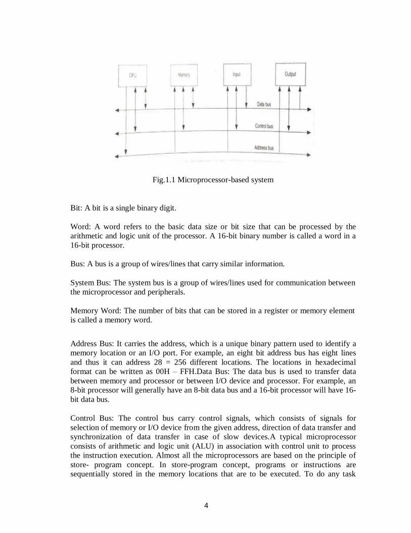
Fig.1.1 Microprocessor-based system
Bit: A bit is a single binary digit.
Word: A word refers to the basic data size or bit size that can be processed by the
arithmetic and logic unit of the processor. A 16-bit binary number is called a word in a
16-bit processor.
Bus: A bus is a group of wires/lines that carry similar information.
System Bus: The system bus is a group of wires/lines used for communication between
the microprocessor and peripherals.
Memory Word: The number of bits that can be stored in a register or memory element
is called a memory word.
Address Bus: It carries the address, which is a unique binary pattern used to identify a
memory location or an I/O port. For example, an eight bit address bus has eight lines
and thus it can address 28 = 256 different locations. The locations in hexadecimal
format can be written as 00H – FFH.Data Bus: The data bus is used to transfer data
between memory and processor or between I/O device and processor. For example, an
8-bit processor will generally have an 8-bit data bus and a 16-bit processor will have 16-
bit data bus.
Control Bus: The control bus carry control signals, which consists of signals for
selection of memory or I/O device from the given address, direction of data transfer and
synchronization of data transfer in case of slow devices.A typical microprocessor
consists of arithmetic and logic unit (ALU) in association with control unit to process
the instruction execution. Almost all the microprocessors are based on the principle of
store- program concept. In store-program concept, programs or instructions are
sequentially stored in the memory locations that are to be executed. To do any task
5
using a microprocessor, it is to be programmed by the user. So the programmer must
have idea about its internal resources, features and supported instructions. Each
microprocessor has a set of instructions, a list which is provided by the microprocessor
manufacturer. The instruction set of a microprocessor is provided in two forms: binary
machine code and mnemonics.
Microprocessor communicates and operates in binary numbers 0 and 1. The set of
instructions in the form of binary patterns is called a machine language and it is difficult
for us to understand. Therefore, the binary patterns are given abbreviated names, called
mnemonics, which forms the assembly language. The conversion of assembly-level
language into binary machine-level language is done by using an application called
assembler.
Technology Used:
The semiconductor manufacturing technologies used for chips are:
• Transistor-Transistor Logic (TTL) • Emitter Coupled Logic (ECL)
• Complementary Metal-Oxide Semiconductor (CMOS)
Classification of Microprocessors:
Based on their specification, application and architecture
microprocessors are classified. Based on size of data bus:
• 4-bit microprocessor
• 8-bit microprocessor
• 16-bit microprocessor
• 32-bit microprocessor
Based on application:
• General-purpose microprocessor- used in general computer system and can be used
by programmer for any
application. Examples, 8085 to Intel Pentium.
• Microcontroller- microprocessor with built-in memory and ports and can be programmed for any
generic

6
control
application. Example, 8051.
• Special-purpose processors- designed to handle special functions required for an
application. Examples, digital signal processors and application-specific integrated
circuit (ASIC) chips.
Based on architecture:
• Reduced Instruction Set Computer (RISC) processors
• Complex Instruction Set Computer (CISC) processors
2. 8085 Microprocessor Architecture
The 8085 microprocessor is an 8-bit processor available as a 40-pin IC package and uses
+5 V for power. It can run at a maximum frequency of 3 MHz. Its data bus width is 8-bit
and address bus width is 16-bit, thus it can address 216 = 64 KB of memory. The
internal architecture of 8085 is shown is Fig. 1.2.
Fig 1.2: 8085 Architecture

7
Arithmetic and Logic Unit
The ALU performs the actual numerical and logical operations such as Addition (ADD),
Subtraction (SUB), AND, OR etc. It uses data from memory and from Accumulator to
perform operations. The results of the arithmetic and logical operations are stored in the
accumulator.
Registers
The 8085 includes six registers, one accumulator and one flag register, as shown in Fig.
1.3. In addition, it has two 16-bit registers: stack pointer and program counter. They are
briefly described as follows.
The 8085 has six general-purpose registers to store 8-bit data; these are identified as B,
C, D, E, H and L. they can be combined as register pairs - BC, DE and HL to perform
some 16-bit operations. The programmer can use these registers to store or copy data
into the register by using data copy instructions.
Fig 1.3: Register Organization
Accumulator
The accumulator is an 8-bit register that is a part of ALU. This register is used to store 8-bit data
and to perform arithmetic and logical operations. The result of an operation is stored in the
accumulator. The accumulator is also identified as register A.
8
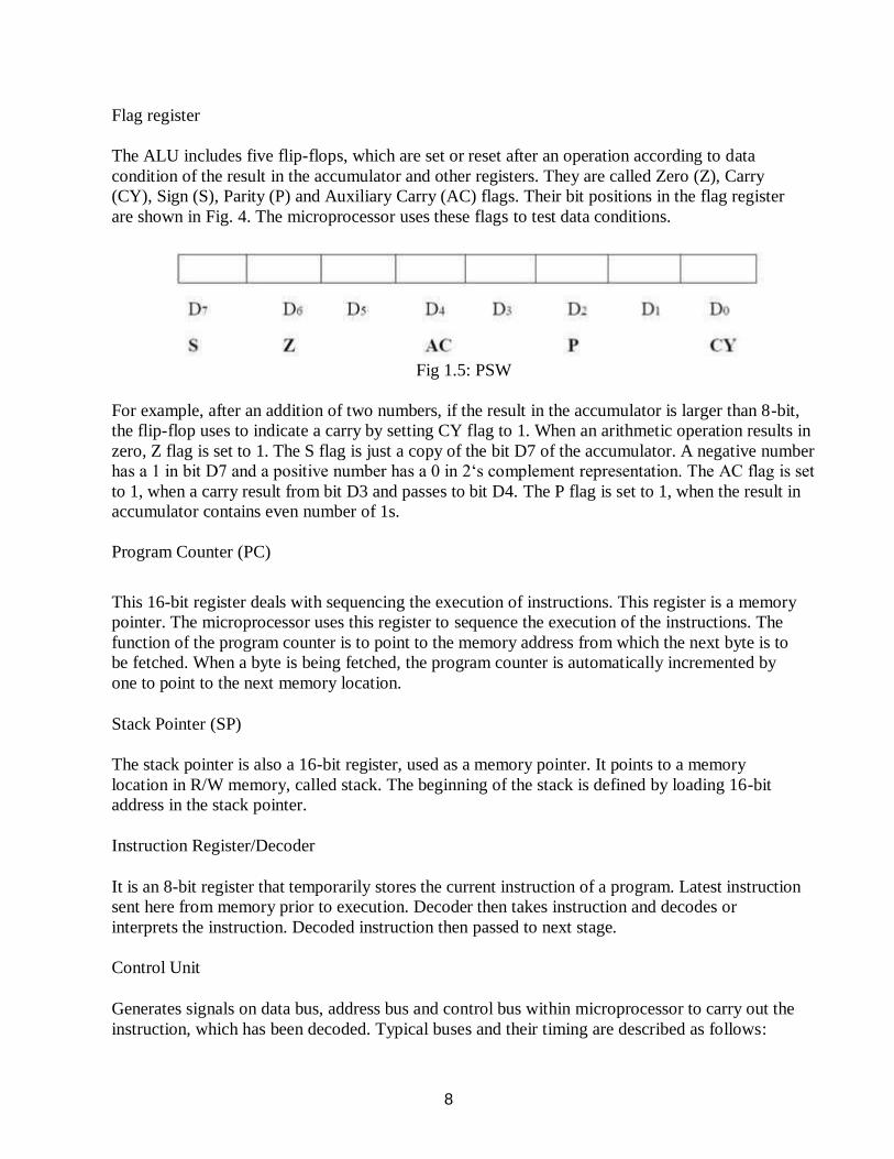
Flag register
The ALU includes five flip-flops, which are set or reset after an operation according to data
condition of the result in the accumulator and other registers. They are called Zero (Z), Carry
(CY), Sign (S), Parity (P) and Auxiliary Carry (AC) flags. Their bit positions in the flag register
are shown in Fig. 4. The microprocessor uses these flags to test data conditions.
Fig 1.5: PSW
For example, after an addition of two numbers, if the result in the accumulator is larger than 8-bit,
the flip-flop uses to indicate a carry by setting CY flag to 1. When an arithmetic operation results in
zero, Z flag is set to 1. The S flag is just a copy of the bit D7 of the accumulator. A negative number
has a 1 in bit D7 and a positive number has a 0 in 2‘s complement representation. The AC flag is set
to 1, when a carry result from bit D3 and passes to bit D4. The P flag is set to 1, when the result in
accumulator contains even number of 1s.
Program Counter (PC)
This 16-bit register deals with sequencing the execution of instructions. This register is a memory
pointer. The microprocessor uses this register to sequence the execution of the instructions. The
function of the program counter is to point to the memory address from which the next byte is to
be fetched. When a byte is being fetched, the program counter is automatically incremented by
one to point to the next memory location.
Stack Pointer (SP)
The stack pointer is also a 16-bit register, used as a memory pointer. It points to a memory
location in R/W memory, called stack. The beginning of the stack is defined by loading 16-bit
address in the stack pointer.
Instruction Register/Decoder
It is an 8-bit register that temporarily stores the current instruction of a program. Latest instruction
sent here from memory prior to execution. Decoder then takes instruction and decodes or
interprets the instruction. Decoded instruction then passed to next stage.
Control Unit
Generates signals on data bus, address bus and control bus within microprocessor to carry out the
instruction, which has been decoded. Typical buses and their timing are described as follows:

9
• Data Bus: Data bus carries data in binary form between microprocessor and other
external units such as memory. It is used to transmit data i.e. information, results of
arithmetic etc between memory and the microprocessor. Data bus is bidirectional in nature. The
data bus width of 8085 microprocessor is 8-bit i.e. 28 combination of binary digits and are typically
identified as D0 – D7. Thus
size of the data bus determines what arithmetic can be done. If only 8-bit wide then largest number
is 11111111 (255 in decimal). Therefore, larger numbers have to be broken down into chunks of
255. This slows
microprocessor.
• Address Bus: The address bus carries addresses and is one way bus from microprocessor
to the memory or other devices. 8085 microprocessor contain 16-bit address bus and are
generally identified as A0 - A15. The higher
order address lines (A8 – A15) are unidirectional and the lower order lines (A0 – A7) are
multiplexed (time- shared) with the eight data bits (D0 – D7) and hence, they are
bidirectional.
• Control Bus: Control bus are various lines which have specific functions for coordinating and
controlling
microprocessor operations. The control bus carries control signals partly unidirectional and
partly bidirectional. The following control and status signals are used by 8085 processor:
I. ALE (output): Address Latch Enable is a pulse that is provided when an
address appears on the AD0 – AD7 lines, after which it becomes 0.
II. RD (active low output): The Read signal indicates that data are being read from
the selected I/O or memory device and that they are available on the data bus.
III. WR (active low output): The Write signal indicates that data on the data bus are
to be written into a selected memory or I/O location.
IV. IO/M (output): It is a signal that distinguished between a memory operation and
an I/O operation. When IO/M = 0 it is a memory operation and IO/M = 1 it is an
I/O operation.
V. S1 and S0 (output): These are status signals used to specify the type of operation
being performed; they are listed in Table 1.1

10
Table 1.1: Status signals and associated operations
The schematic representation of the 8085 bus structure is as shown in Fig. 1.5.
The microprocessor performs primarily four operations:
1.Memory Read: Reads data (or instruction)
from memory. 2.Memory Write: Writes data
(or instruction) into memory. 3.I/O Read:
Accepts data from input device.
4.I/O Write: Sends data to output device.
The 8085 processor performs these functions using address bus, data bus and control
bus as shown in Fig. 1.5.
Fig 1.5: 8085 Bus structure
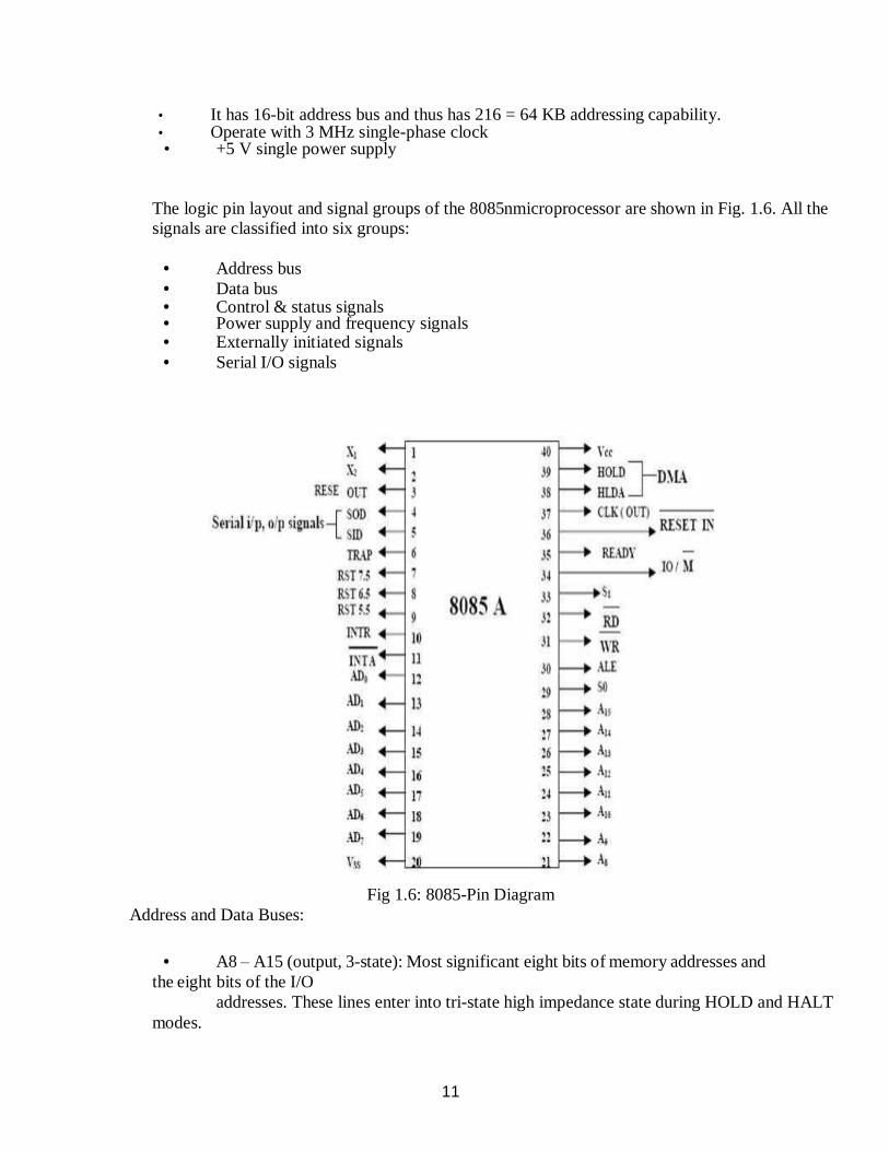
3. 8085 Pin Description
• It is a 8-bit microprocessor • Manufactured with N-MOS technology • 40 pin IC package
11
• It has 16-bit address bus and thus has 216 = 64 KB addressing capability. • Operate with 3 MHz single-phase clock • +5 V single power supply
The logic pin layout and signal groups of the 8085nmicroprocessor are shown in Fig. 1.6. All the
signals are classified into six groups:
• Address bus
• Data bus • Control & status signals • Power supply and frequency signals • Externally initiated signals
• Serial I/O signals
Fig 1.6: 8085-Pin Diagram
Address and Data Buses:
• A8 – A15 (output, 3-state): Most significant eight bits of memory addresses and
the eight bits of the I/O
addresses. These lines enter into tri-state high impedance state during HOLD and HALT
modes.

12
• AD0 – AD7 (input/output, 3-state): Lower significant bits of memory
addresses and the eight bits of the I/O addresses during first clock cycle.
Behaves as data bus during third and fourth clock cycle. These lines enter into
tri-state high impedance state during HOLD and HALT modes.
Control & Status Signals:
• ALE: Address latch enable
• RD : Read control signal.
• WR :Write control signal
:
• IO/M , S1 and S0 : Status
signals. Power Supply & Clock Frequency:
• Vcc: +5 V power supply
• Vss: Ground reference
• X1, X2: A crystal having frequency of 6 MHz is connected at these two pins
• CLK: Clock output
Externally Initiated and Interrupt Signals:
• RESET IN : When the signal on this pin is low, the PC is set to 0, the buses are
tri-stated and the processor is reset.
• RESET OUT: This signal indicates that the processor is being reset. The
signal can be used to reset other
devices.
• READY: When this signal is low, the processor waits for an integral number
of clock cycles until it goes high.
• HOLD: This signal indicates that a peripheral like DMA (direct
memory access) controller is requesting the use of address and data bus.
• HLDA: This signal acknowledges the HOLD request.
• INTR: Interrupt request is a general-purpose interrupt.
• INTA : This is used to acknowledge an interrupt.
• RST 7.5, RST 6.5, RST 5,5 – restart interrupt: These are vectored interrupts

13
and have highest priority than INTR interrupt.
• TRAP: This is a non-maskable interrupt and has the highest priority.
Serial I/O Signals:
• SID: Serial input signal. Bit on this line is loaded to D7 bit of register A
using RIM instruction.
• SOD: Serial output signal. Output SOD is set or reset by using SIM instruction.
4. Instruction Set And Execution In 8085
Based on the design of the ALU provides and decoding unit, the microprocessor manufacturer
microprocessor. The instruction set for every machine code and instruction set
consists of both
mnemonics.
An instruction is a binary pattern designed inside a microprocessor to perform a
specific function. The entire group of instructions that a microprocessor
supports is called instruction set. Microprocessor instructions can be classified
based on the parameters such functionality, length and operand addressing.
Classification based on functionality:
I. Data transfer operations: This group of instructions copies data from source to
destination. The content of the source is not altered.
II. Arithmetic operations: Instructions of this group perform operations like
addition, subtraction, increment & decrement. One of the data used in
arithmetic operation is stored in accumulator and the result is also stored in
accumulator.
III. Logical operations: Logical operations include AND, OR, EXOR, NOT. The
operations like AND, OR and EXOR uses two operands, one is stored in
accumulator and other can be any register or memory location. The result is
stored in accumulator. NOT operation requires single operand, which is stored
in accumulator.
IV. Branching operations: Instructions in this group can be used to transfer
program sequence from one memory location to another either conditionally or
unconditionally.
V. Machine control operations: Instruction in this group control execution of
other instructions and control operations like interrupt, halt etc.

14
Classification based on length:
I. One-byte instructions: Instruction having one byte in machine code. Examples are
depicted in Table 1.2.
I. Two-byte instructions: Instruction having two byte in machine code. Examples
are depicted in Table 1.3
II. Three-byte instructions: Instruction having three byte in machine code.
Examples are depicted in Table 1.4.
Table 1.2: Example of one byte instruction
Opcode Operand Machine code/Hex code
MOV A, B 78
ADD M 86
Table 1.3 Examples of two byte instructions
Opcode Operand Machine code/Hex code Byte description
MVI A, 7FH 3E First byte
7F Second byte
ADI 0FH C6 First byte
0F Second byte
Table 1.4 Examples of
three byte instructions
Opcode Operand Machine code/Hex code Byte description
JMP 9050H C3 First byte
50 Second byte
90 Third byte
LDA 8850H 3A First byte
50 Second byte
88 Third byte
5.Addressing Modes in Instructions:
The process of specifying the data to be operated on by the instruction is called
addressing. The various formats for specifying operands are called addressing modes.
The 8085 has the following five types of addressing:
1. Immediate addressing
2. Memory direct addressing
3. Register direct addressing
15
4. Indirect addressing
5. Implicit
addressing Immediate
Addressing:
In this mode, the operand given in the instruction - a byte or word – transfers to the
destination register or memory location.
Ex: MVI A, 9AH
• The operand is a part of the instruction.
• The operand is stored in the register mentioned in the instruction.
Memory Direct Addressing:
Memory direct addressing moves a byte or word between a memory location and
register. The memory location address is given in the instruction.
Ex: LDA 850FH
This instruction is used to load the content of memory address 850FH in the
accumulator. Register Direct Addressing:
Register direct addressing transfer a copy of a byte or word from source register to
destination register.
Ex: MOV B, C
It copies the content of register C to register B.
Indirect Addressing:
Indirect addressing transfers a byte or word between a register and a memory
location. Ex: MOV A, M
Here the data is in the memory location pointed to by the contents of HL pair. The data
is moved to the accumulator.
Implicit Addressing
In this addressing mode the data itself specifies the data to be
operated upon. Ex: CMA

16
The instruction complements the content of the accumulator. No specific data or
operand is mentioned in the instruction
6.Instruction Execution and Timing Diagram
Each instruction in 8085 microprocessor consists of two part- operation code (opcode)
and operand. The opcode is a command such as ADD and the operand is an object to be
operated on, such as a byte or the content of a register.
Instruction Cycle: The time taken by the processor to complete the execution of an
instruction. An instruction cycle consists of one to six machine cycles.
Machine Cycle: The time required to complete one operation; accessing either the
memory or I/O device. A machine cycle consists of three to six T-states.
T-State: Time corresponding to one clock period. It is the basic unit to calculate
execution of instructions or programs in a processor.
To execute a program, 8085 performs various operations as:
• Opcode fetch
• Operand fetch
• Memory read/write
• I/O read/write
External communication functions are:
• Memory read/write
• I/O read/write
• Interrupt request acknowledge
Opcode Fetch Machine Cycle:
It is the first step in the execution of any instruction. The timing diagram of this cycle
is given in Fig. 1.7.
The following points explain the various operations that take place and the signals
that are changed during the execution of opcode fetch machine cycle:
T1 clock cycle
i. The content of PC is placed in the address bus; AD0 - AD7 lines contains lower bit
address and A8 – A15 contains higher bit address.
ii. IO/M signal is low indicating that a memory location is being accessed. S1
and S0 also changed to the levels as indicated in Table 1.

17
iii. ALE is high, indicates that multiplexed AD0 – AD7 act as lower order bus.
T2 clock cycle
i. Multiplexed address bus is now changed to data bus.
ii. The RD signal is made low by the processor. This signal makes the memory
device load the data bus with the contents of the location addressed by the processor. T3 clock cycle
i. The opcode available on the data bus is read by the processor and moved to the
instruction register.
ii. The RD signal is deactivated by making it logic 1.
T4 clock cycle
i. The processor decode the instruction in the instruction register and generate the
necessary control signals to execute the instruction. Based on the instruction further
operations such as fetching, writing into memory etc takes place.
Fig. 1.7 Timing diagram for opcode fetch cycle
Memory Read Machine Cycle:
The memory read cycle is executed by the processor to read a data byte from memory.
The machine cycle is exactly same to opcode fetch except: a) It has three T-states b) The
S0 signal is set to 0. The timing diagram of this cycle is given in Fig. 1.8.
18
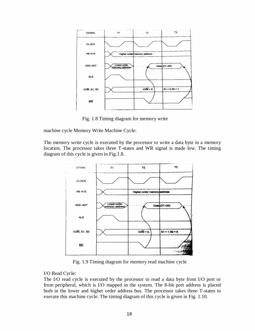
Fig. 1.8 Timing diagram for memory write
machine cycle Memory Write Machine Cycle:
The memory write cycle is executed by the processor to write a data byte in a memory
location. The processor takes three T-states and WR signal is made low. The timing
diagram of this cycle is given in Fig.1.8.
Fig. 1.9 Timing diagram for memory read machine cycle
I/O Read Cycle:
The I/O read cycle is executed by the processor to read a data byte from I/O port or
from peripheral, which is I/O mapped in the system. The 8-bit port address is placed
both in the lower and higher order address bus. The processor takes three T-states to
execute this machine cycle. The timing diagram of this cycle is given in Fig. 1.10.

19
Fig.1. 10 Timing diagram I/O read machine cycle
I/O Write Cycle:
The I/O write cycle is executed by the processor to write a data byte to I/O port or to a
peripheral, which is I/O mapped in the system. The processor takes three T-states to
execute this machine cycle. The timing diagram of this cycle is given in Fig. 1.11.
Fig.1. 11 Timing diagram I/O write machine cycle
20
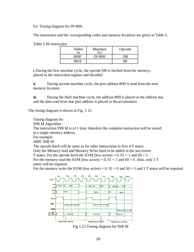
Ex: Timing diagram for IN 80H.
The instruction and the corresponding codes and memory locations are given in Table 5.
Table 5 IN instruction
Address
Mnemonics
Opcode
800F IN 80H DB
8010 80
i. During the first machine cycle, the opcode DB is fetched from the memory,
placed in the instruction register and decoded.
ii. During second machine cycle, the port address 80H is read from the next
memory location.
iii. During the third machine cycle, the address 80H is placed in the address bus
and the data read from that port address is placed in the accumulator.
The timing diagram is shown in Fig. 1.12.
Timing diagram for
INR M Algorithm –
The instruction INR M is of 1 byte; therefore the complete instruction will be stored
in a single memory address.
For example:
2000: INR M
The opcode fetch will be same as for other instructions in first 4 T states.
Only the Memory read and Memory Write need to be added in the successive
T states. For the opcode fetch the IO/M (low active) = 0, S1 = 1 and S0 = 1.
For the memory read the IO/M (low active) = 0, S1 = 1 and S0 = 0. Also, only 3 T
states will be required.
For the memory write the IO/M (low active) = 0, S1 = 0 and S0 = 1 and 3 T states will be required.
Fig 1.12 Timing diagram for INR M
21
In Opcode fetch ( t1-t4 T states ) –
• 00: lower bit of address where opcode is stored, i.e., 00
• 20: higher bit of address where opcode is stored, i.e., 20.
• ALE: provides signal for multiplexed address and data bus. Only in t1 it used as
address bus to fetch lower bit of address otherwise it will be used as data bus.
• RD (low active): signal is 1 in t1 & t4 as no data is read by microprocessor. Signal is 0
in t2 & t3 because here the data is read by microprocessor.
• WR (low active): Signal is 1 throughout, no data is written by microprocessor.
• IO/M (low active): Signal is 0 in throughout because the operation is performing on memory.
• S0 and S1: both are 1 in case of opcode
fetching. In Memory read ( t5-t7 T states )
–
• 00: lower bit of address where opcode is stored, i.e, 00
• 50: higher bit of address where opcode is stored, i.e, 50.
• ALE: provides signal for multiplexed address and data bus. Only in t5 it used as
address bus to fetch lower bit of address otherwise it will be used as data bus.
• RD (low active): signal is 1 in t5, no data is read by microprocessor. Signal is 0 in t6
& t7, data is read by microprocessor.
• WR (low active): signal is 1 throughout, no data is written by microprocessor.
• IO/M (low active): signal is 0 in throughout, operation is performing on memory.
• S0 and S1 – S1=1 and S0=0 for Read
operation. In Memory write ( t8-t10 T
states ) – • 00: lower bit of address where opcode is stored, i.e, 00 • 50: higher bit of address where opcode is stored, i.e, 50.
• ALE: provides signal for multiplexed address and data bus. Only in t8 it used as
address bus to fetch lower bit of address otherwise it will be used as data bus.
• RD (low active): signal is 1 throughout, no data is read by microprocessor.
• WR (low active): signal is 1 in t8, no data is written by microprocessor. Signal is 0 in
t9 & t10, data is written by microprocessor.
• IO/M (low active): signal is 0 in throughout, operation is performing on memory.
• S0 and S1 – S1=0 and S0=1 for write operation.
Timing diagram of MVI instruction
Problem – Draw the timing diagram of the
following code, MVI B, 45
Explanation of the command – It stores the immediate 8 bit data to a register or memory
location. Example: MVI B, 45
Opcode: MVI Operand: B is the destination register and 45 is the source data which needs to be
transferred to the register.
‘45‘ data is stored in the B
register. Algorithm –
• Decide what is the opcode and what is the data. Here, opcode is ‗MVI B‘ and data is 45. • Assume the memory address of the opcode and the data. For
example: MVI B, 45

22
2000: Opcode
2001: 45
• The opcode fetch will be same in all the instructions.
• Only the read instruction of the opcode needs to be added in the successive T states.
• For the opcode read the IO/M (low active) = 0, S1 = 1 and S0 = 0. Also, only 3 T
states will be required.
Fig 1.13: timing diagram for
MVI B,45 Timing diagram of MOV Instruction in
Microprocessor
Problem – Draw the timing diagram of the given instruction
in 8085, MOV B, C
Given instruction copies the contents of the source register into the destination register
and the contents of the source register are not altered
OV B, C
Opcode:
MOV
Operand: B
and C
Bis the destination register and C is the source register whose contents need to be
transferred to the destination register.
Algorithm –
The instruction MOV B, C is of 1 byte; therefore the complete instruction will be stored in
a single memory address. For example:
2000: MOV B, C
Only opcode fetching is required for this instruction and thus we need 4 T states for
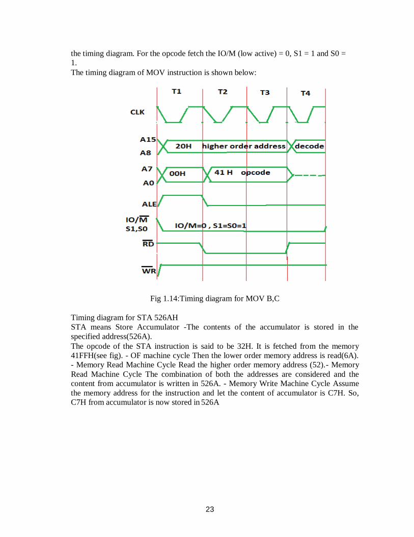
23
the timing diagram. For the opcode fetch the IO/M (low active) = 0, S1 = 1 and S0 =
1.
The timing diagram of MOV instruction is shown below:
Fig 1.14:Timing diagram for MOV B,C
Timing diagram for STA 526AH
STA means Store Accumulator -The contents of the accumulator is stored in the
specified address(526A).
The opcode of the STA instruction is said to be 32H. It is fetched from the memory
41FFH(see fig). - OF machine cycle Then the lower order memory address is read(6A).
- Memory Read Machine Cycle Read the higher order memory address (52).- Memory
Read Machine Cycle The combination of both the addresses are considered and the
content from accumulator is written in 526A. - Memory Write Machine Cycle Assume
the memory address for the instruction and let the content of accumulator is C7H. So,
C7H from accumulator is now stored in 526A
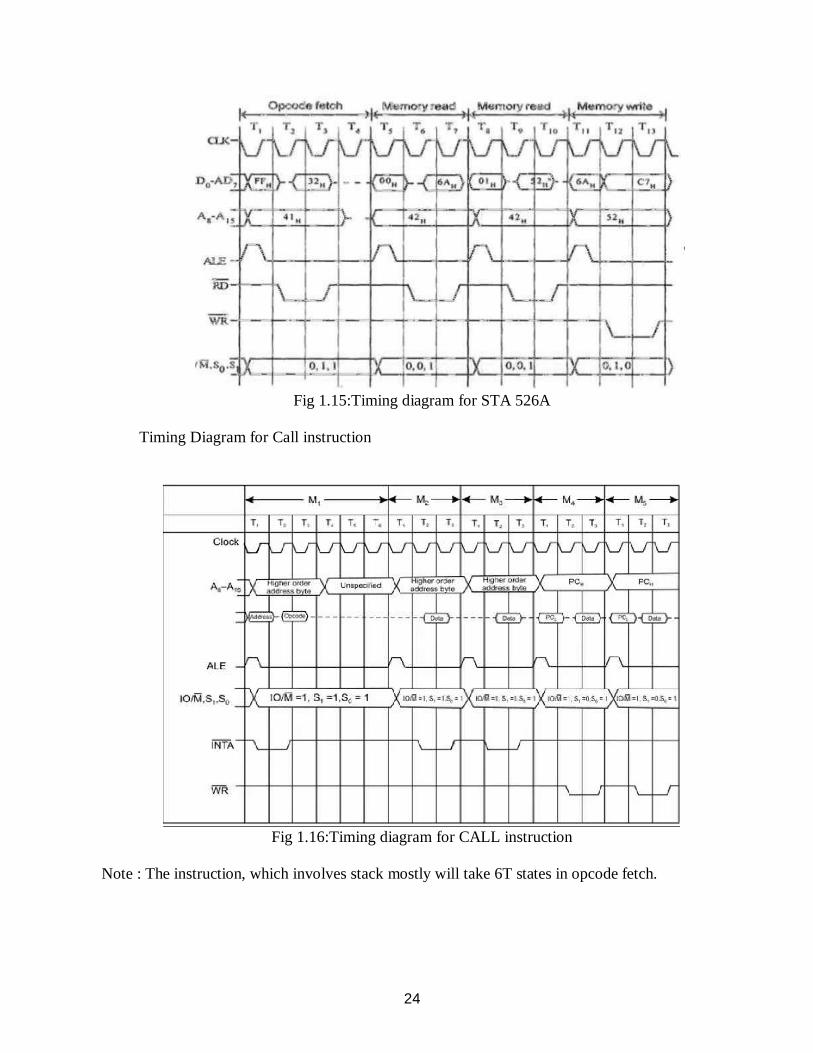
24
Fig 1.15:Timing diagram for STA 526A
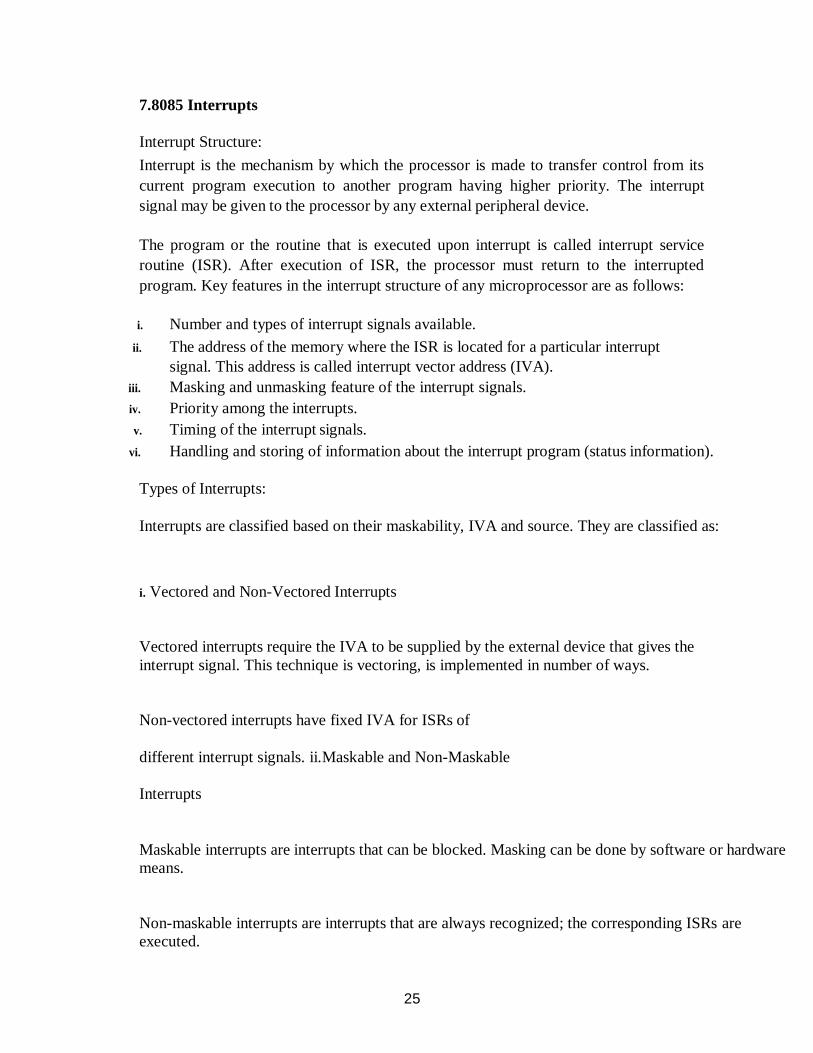
Timing Diagram for Call instruction
Fig 1.16:Timing diagram for CALL instruction
Note : The instruction, which involves stack mostly will take 6T states in opcode fetch.
25
7.8085 Interrupts
Interrupt Structure:
Interrupt is the mechanism by which the processor is made to transfer control from its
current program execution to another program having higher priority. The interrupt
signal may be given to the processor by any external peripheral device.
The program or the routine that is executed upon interrupt is called interrupt service
routine (ISR). After execution of ISR, the processor must return to the interrupted
program. Key features in the interrupt structure of any microprocessor are as follows:
i. Number and types of interrupt signals available.
ii. The address of the memory where the ISR is located for a particular interrupt
signal. This address is called interrupt vector address (IVA).
iii. Masking and unmasking feature of the interrupt signals.
iv. Priority among the interrupts.
v. Timing of the interrupt signals.
vi. Handling and storing of information about the interrupt program (status information).
Types of Interrupts:
Interrupts are classified based on their maskability, IVA and source. They are classified as:
i. Vectored and Non-Vectored Interrupts
Vectored interrupts require the IVA to be supplied by the external device that gives the
interrupt signal. This technique is vectoring, is implemented in number of ways.
Non-vectored interrupts have fixed IVA for ISRs of
different interrupt signals. ii.Maskable and Non-Maskable
Interrupts
Maskable interrupts are interrupts that can be blocked. Masking can be done by software or hardware
means.
Non-maskable interrupts are interrupts that are always recognized; the corresponding ISRs are
executed.

26
iii. Software and Hardware Interrupts
Software interrupts are special instructions, after execution transfer the control to predefined ISR.
Hardware interrupts are signals given to the processor, for recognition as an interrupt
and execution of the corresponding ISR.
Interrupt Handling Procedure:
The following sequence of operations takes place when an interrupt signal is recognized:
i. Save the PC content and information about current state (flags,
registers etc) in the stack. ii.Load PC with the beginning address of
an ISR and start to execute it.
iii. Finish ISR when the return instruction is executed.
iv. Return to the point in the interrupted program where execution was interrupted.
Interrupt Sources and Vector Addresses in 8085:
Software Interrupts:
8085 instruction set includes eight software interrupt instructions called Restart (RST)
instructions. These are one byte instructions that make the processor execute a
subroutine at predefined locations. Instructions and their vector addresses are given in
Table 1.6
Table 1.6 Vector address
Instruction
Machine hex code
Interrupt Vector Address
RST 0 C7 0000H
RST 1 CF 0008H
RST 2 D7 0010H
RST 3 DF 0018H
RST 4 E7 0020H
RST 5 EF 0028H
RST 6 F7 0030H
RST 7 FF 0032H
The software interrupts can be treated as CALL instructions with default call locations.
The concept of priority does not apply to software interrupts as they are inserted into the
27
program as instructions by the programmer and executed by the processor when the
respective program lines are read.
Hardware Interrupts and Priorities:
8085 have five hardware interrupts – INTR, RST 5.5, RST 6.5, RST 7.5 and TRAP.
Their IVA and priorities are given in Table 1.7.
Table 1.7 Hardware interrupts of 8085
Interrupt Interrupt
vector
address
Maskable or
non-
maskable
Edge or
level
Triggered
priority
TRAP 0024H Non-makable
Level 1
RST 7.5 003CH Maskable Rising edge 2
RST 6.5 0034H Maskable Level 3
RST 5.5 002CH Maskable Level 4
INTR Decided by hardware Maskable Level 5
Masking of Interrupts:
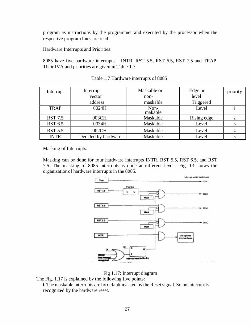
Masking can be done for four hardware interrupts INTR, RST 5.5, RST 6.5, and RST
7.5. The masking of 8085 interrupts is done at different levels. Fig. 13 shows the
organization of hardware interrupts in the 8085.
Fig 1.17: Interrupt diagram
The Fig. 1.17 is explained by the following five points:
i. The maskable interrupts are by default masked by the Reset signal. So no interrupt is
recognized by the hardware reset.
28
ii. The interrupts can be enabled by the EI instruction.
iii. The three RST interrupts can be selectively masked by loading the appropriate
word in the accumulator and executing SIM instruction. This is called software masking.
iv. All maskable interrupts are disabled whenever an interrupt is recognized.
v. All maskable interrupts can be disabled by executing the DI instruction.
RST 7.5 alone has a flip-flop to recognize edge transition. The DI instruction reset
interrupt enable flip-flop in the processor and the interrupts are disabled. To enable
interrupts, EI instruction has to be executed.
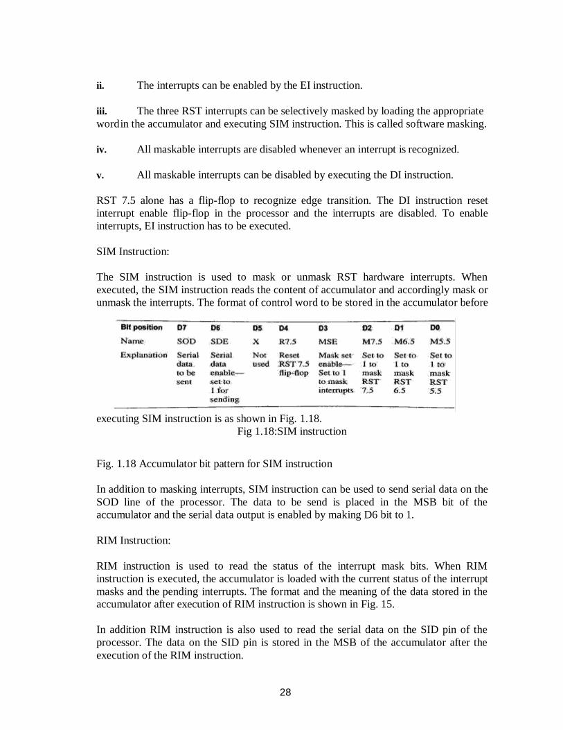
SIM Instruction:
The SIM instruction is used to mask or unmask RST hardware interrupts. When
executed, the SIM instruction reads the content of accumulator and accordingly mask or
unmask the interrupts. The format of control word to be stored in the accumulator before
executing SIM instruction is as shown in Fig. 1.18.
Fig 1.18:SIM instruction
Fig. 1.18 Accumulator bit pattern for SIM instruction
In addition to masking interrupts, SIM instruction can be used to send serial data on the
SOD line of the processor. The data to be send is placed in the MSB bit of the
accumulator and the serial data output is enabled by making D6 bit to 1.
RIM Instruction:
RIM instruction is used to read the status of the interrupt mask bits. When RIM
instruction is executed, the accumulator is loaded with the current status of the interrupt
masks and the pending interrupts. The format and the meaning of the data stored in the
accumulator after execution of RIM instruction is shown in Fig. 15.
In addition RIM instruction is also used to read the serial data on the SID pin of the
processor. The data on the SID pin is stored in the MSB of the accumulator after the
execution of the RIM instruction.
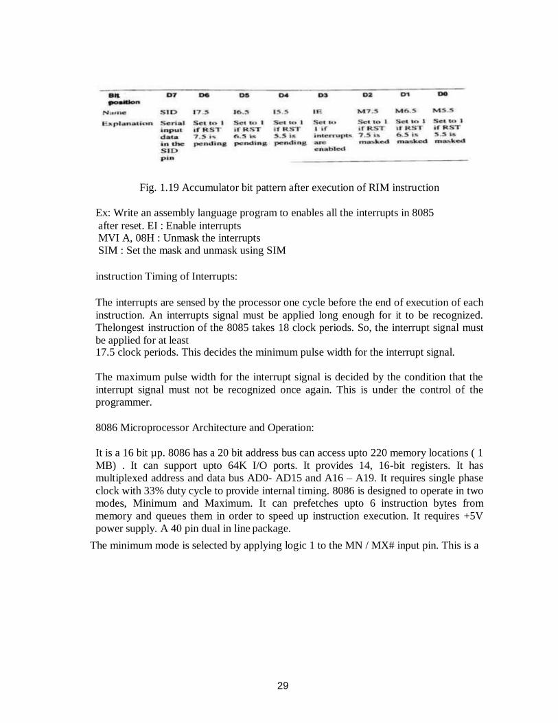
29
Fig. 1.19 Accumulator bit pattern after execution of RIM instruction
Ex: Write an assembly language program to enables all the interrupts in 8085
after reset. EI : Enable interrupts MVI A, 08H : Unmask the interrupts
SIM : Set the mask and unmask using SIM
instruction Timing of Interrupts:
The interrupts are sensed by the processor one cycle before the end of execution of each
instruction. An interrupts signal must be applied long enough for it to be recognized.
Thelongest instruction of the 8085 takes 18 clock periods. So, the interrupt signal must
be applied for at least 17.5 clock periods. This decides the minimum pulse width for the interrupt signal.
The maximum pulse width for the interrupt signal is decided by the condition that the
interrupt signal must not be recognized once again. This is under the control of the
programmer.
8086 Microprocessor Architecture and Operation:
It is a 16 bit µp. 8086 has a 20 bit address bus can access upto 220 memory locations ( 1
MB) . It can support upto 64K I/O ports. It provides 14, 16-bit registers. It has
multiplexed address and data bus AD0- AD15 and A16 – A19. It requires single phase
clock with 33% duty cycle to provide internal timing. 8086 is designed to operate in two
modes, Minimum and Maximum. It can prefetches upto 6 instruction bytes from
memory and queues them in order to speed up instruction execution. It requires +5V
power supply. A 40 pin dual in line package.
The minimum mode is selected by applying logic 1 to the MN / MX# input pin. This is a

30
single microprocessor configuration. The maximum mode is selected by applying
logic 0 to the MN / MX# input pin. This is a multi micro processors configuration.
8.Block diagram of 8086
Fig 1.20 Block diagram of 8086
microprocessor Software model of 8086
Fig 1.21 Software model-8086

31
Fig 1.22: General purpose
registers Internal Architecture of 8086
8086 has two blocks BIU and EU. The BIU performs all bus operations such as
instruction fetching, reading and writing operands for memory and calculating the
addresses of the memory operands. The instruction bytes are transferred to the
instruction queue. EU executes instructions from the instruction system byte queue.
Both units operate asynchronously to give the 8086 an overlapping instruction fetch
and execution mechanism which is called as Pipelining. This results in efficient use of
the system bus and system performance. BIU contains Instruction queue, Segment
registers, Instruction pointer, Address adder. EU contains Control circuitry, Instruction
decoder, ALU, Pointer and Index register, Flag register.
Bus Interfacr Unit:
It provides a full 16 bit bidirectional data bus and 20 bit address bus. The bus interface
unit is responsible for performing all external bus operations.
Specifically it has the following functions:
Instruction fetch, Instruction queuing, Operand fetch and storage, Address relocation
and Bus control. The BIU uses a mechanism known as an instruction stream queue to
implement a pipeline architecture.

32
This queue permits prefetch of up to six bytes of instruction code. When ever the
queue of the BIU is not full, it has room for at least two more bytes and at the same
time the EU is not requesting it to read or write operands from memory, the BIU is
free to look ahead in the program by prefetching the next sequential instruction.
These prefetching instructions are held in its FIFO queue. With its 16 bit data bus, the
BIU fetches two instruction bytes in a single memory cycle. After a byte is loaded at
the input end of the queue, it automatically shifts up through the FIFO to the empty
location nearest the output.
The EU accesses the queue from the output end. It reads one instruction byte after the
other from the output of the queue. If the queue is full and the EU is not requesting
access to operand in memory. These intervals of no bus activity, which may occur
between bus cyclesare known as Idle state. If the BIU is already in the process of
fetching an instruction when the EU request it to read or write operands from memory
or I/O, the BIU first completes theinstruction fetch bus cycle before initiating the
operand read
/ write cycle. The BIU also contains a dedicated adder which is used to generate the
20 bit physical address that is output on the address bus. This address is formed by
adding an appended 16 bit segment address and a 16 bit offset address. For example,
the physical address of the next instructionto be fetched is formed by combining the
current contents of the code segment CS register and the current contents of the
instruction pointer IP register. The BIU is also responsible for generating bus control
signals such as those for memory read or write and I/O read or write.
EXECUTION UNIT : The Execution unit is responsible for decoding and executing
all instructions. The EU extracts instructions from the top of the queue in the BIU,
decodes them, generates operands if necessary, passes them to the BIU and requests it to
perform theread or write bys cycles to memory or I/O and perform the operation
specified by the instruction on the operands. During the execution of the instruction,
the EU tests the status and control flags and updates them based on the results of
executing the instruction. If the queue is empty, the EU waits for the next instruction
byte to be fetched and shifted to top ofthe queue. When the EU executes a branch or
jump instruction, it transfers control to a location corresponding to another set of
sequential instructions. Whenever this happens, the BIU automatically resets the queue
and then begins to fetch instructions from this new location to refill the queue.
33
Internal Registers of 8086
The 8086 has four groups of the user accessible internal registers. They are the
instruction pointer, four data registers, four pointer and index register, four segment
registers.
The 8086 has a total of fourteen 16-bit registers including a 16 bit register called the
status register, with 9 of bits implemented for status and control flags. Most of the
registers contain data/instruction offsets within 64 KB memory segment. There are four
different 64 KB segments for instructions, stack, data and extra data. To specify where
in 1 MB of processor memory these 4 segments are located the processor uses four
segment registers:
Code segment (CS) is a 16-bit register containing address of 64 KB segment with
processorinstructions. The processor uses CS segment for all accesses to instructions
referenced by instruction pointer (IP) register. CS register cannot be changed directly.
The CS register is automatically updated during far jump, far call and far return
instructions.
Stack segment (SS) is a 16-bit register containing address of 64KB segment with
program stack. By default, the processor assumes that all data referenced by the stack
pointer (SP) and base pointer (BP) registers is located in the stack segment. SS
register can be changed directly using POP instruction.
Data segment (DS) is a 16-bit register containing address of 64KB segment with
program data. By default, the processor assumes that all data referenced by general
registers (AX, BX, CX, DX) and index register (SI, DI) is located in the data segment.
DS register can be changed directly using POP and LDS instructions.
Extra segment (ES) is a 16-bit register containing address of 64KB segment, usually
with program data. By default, the processor assumes that the DI register references
the ES

34
segment in string manipulation instructions. ES register can be changed directly using
POP and LES instructions. It is possible to change default segments used by general
and index registers by prefixing instructions with a CS, SS, DS or ES prefix.
All general registers of the 8086 microprocessor can be used for arithmetic and logic
operations. The general registers are:
Accumulator register consists of two 8-bit registers AL and AH, which can be
combined together and used as a 16-bit register AX. AL in this case contains the low-
order byte of the word, and AH contains the high-order byte. Accumulator can be used
for I/O operations andstring manipulation.
Base register consists of two 8-bit registers BL and BH, which can be combined
together and used as a 16-bit register BX. BL in this case contains the low-order byte of
the word, and BH contains the high-order byte. BX register usually contains a data
pointer used for based, based indexed or register indirect addressing.
Count register consists of two 8-bit registers CL and CH, which can be combined
together and used as a 16-bit register CX. When combined, CL register contains the
low-order byteof the word, and CH contains the high-order byte. Count register canbe
used in Loop, shift/rotate instructions and as a counter in string manipulation,.
Data register consists of two 8-bit registers DL and DH, which can be combined
together and used as a 16-bit register DX. When combined, DL register contains the
low-order byte of the word, and DH contains the high- order byte. Data register can be
used as a port number in I/O operations. In integer 32-bit multiply and divide
instruction the DX register contains high-order word of the initial or resulting number.
The following registers are both general and index registers:
Stack Pointer (SP) is a 16-bit register pointing to program stack.
Base Pointer (BP) is a 16-bit register pointing to data in stack segment. BP register is
usually used for based, based indexed or register indirect addressing.
Source Index (SI) is a 16-bit register. SI is used for indexed, based indexed and
register indirect addressing, as well as a source data address in string manipulation
instructions.
Destination Index (DI) is a 16-bit register. DI is used for indexed, based indexed and
register indirect addressing, as well as a destination data address in string manipulation
instructions.
Other registers:
Instruction Pointer (IP) is a 16-bit register.Flags is a 16-bit register containing 9 one bit flags.

35
Overflow Flag (OF) - set if the result is too large positive number, or is too small
negativenumber to fit into destination operand.
Direction Flag (DF) - if set then string manipulation instructions will auto-
decrement indexregisters. If cleared then the index registers will be auto-
incremented.
Interrupt-enable Flag (IF) - setting this bit enables maskable interrupts.
Single-step Flag (TF) - if set then single-step interrupt will occur after the next instruction.
Sign Flag (SF) - set if the most significant bit of the result is
set. Zero Flag (ZF) - set if the result is zero
Auxiliary carry Flag (AF) - set if there was a carry from or borrow to bits 0-3 in
the AL register.
Parity Flag (PF) - set if parity (the number of "1" bits) in the low-order byte of
the result iseven.
Carry Flag (CF) - set if there was a carry from or borrow to the most significant
bit duringlast result calculation.
Addressing Modes
Implied - the data value/data address is implicitly associated with the instruction.
Register - references the data in a register or in a register pair.
Immediate - the data is provided in the instruction.
Direct - the instruction operand specifies the memory address where data is located.
Register indirect - instruction specifies a register containing an address, where data
is located. This addressing mode works with SI, DI, BX and BP registers.
Based :- 8-bit or 16-bit instruction operand is added to the contents of a base
register (BXor BP), the resulting value is a pointer to location where data resides.
Indexed :- 8-bit or 16-bit instruction operand is added to the contents of an
index register(SI or DI), the resulting value is a pointer to location where data
resides.

36
Based Indexed :- the contents of a base register (BX or BP) is added to the contents
of anindex register (SI or DI), the resulting value is a pointer to location where data
resides.
Based Indexed with displacement :- 8-bit or 16-bit instruction operand is added to the
contents of a base register (BX or BP) and index register (SI or DI), the resulting
value is a pointer to location where data resides.
Interrupts
The processor has the following interrupts:
INTR is a maskable hardware interrupt. The interrupt can be enabled/disabled using
STI/CLI instructions or using more complicated method of updating the FLAGS
register with the help of the POPF instruction.
When an interrupt occurs, the processor stores FLAGS register into stack, disables
further interrupts, fetches from the bus one byte representing interrupt type, and jumps
to interrupt processing routine address of which is stored in location 4 * <interrupt
type>. Interrupt processing routine should return with the IRET instruction.
NMI is a non-maskable interrupt. Interrupt is processed in the same way as the INTR
interrupt. Interrupt type of the NMI is 2, i.e. the address of the NMI processing routine
is stored in location 0008h. This interrupt has higher priority then the maskable
interrupt.
Software interrupts can be caused by:
INT instruction - breakpoint interrupt. This is a type 3 interrupt.
INT <interrupt number> instruction - any one interrupt from available 256
interrupts.INTO instruction - interrupt on overflow
Single-step interrupt - generated if the TF flag is set. This is a type 1 interrupt. When
the CPU processes this interrupt it clears TF flag before calling the interrupt
processing routine.
Processor exceptions: Divide Error (Type 0),
Unused Opcode (type 6) and Escape opcode
(type 7).
Software interrupt processing is the same as for the hardware interrupts.
The figure below shows the 256 interrupt vectors arranged in the interrupt vector
table inthe memory.
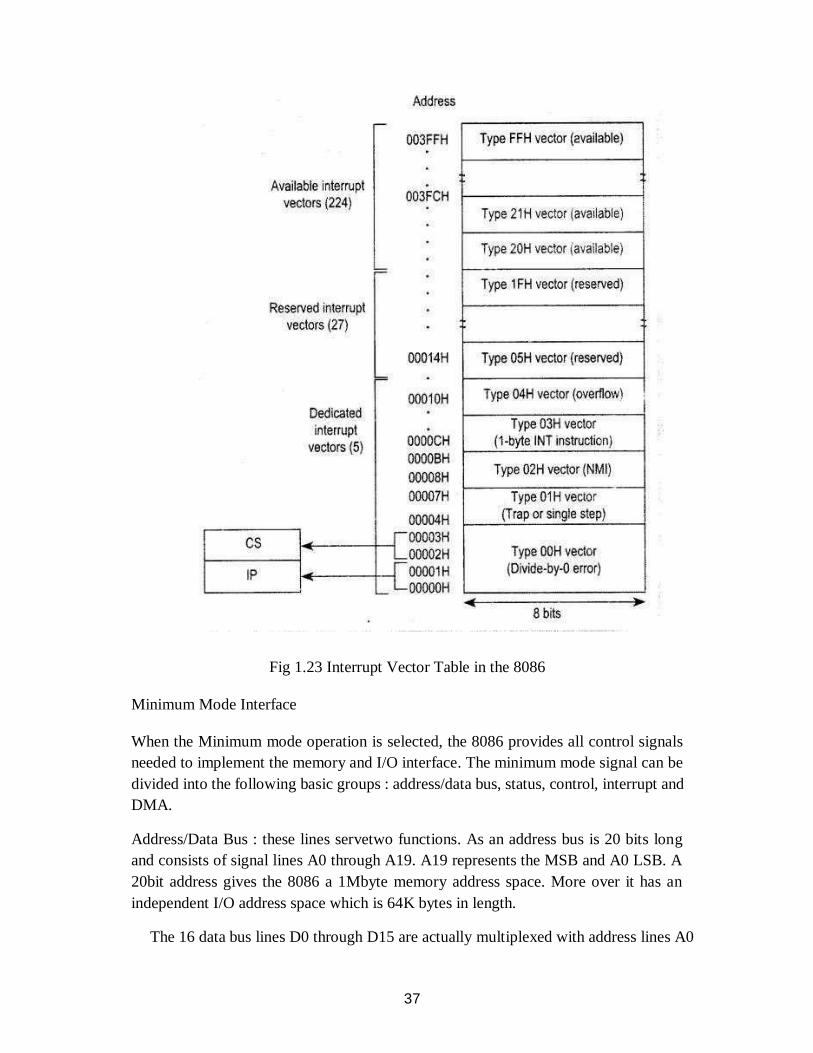
37
Fig 1.23 Interrupt Vector Table in the 8086
Minimum Mode Interface
When the Minimum mode operation is selected, the 8086 provides all control signals
needed to implement the memory and I/O interface. The minimum mode signal can be
divided into the following basic groups : address/data bus, status, control, interrupt and
DMA.
Address/Data Bus : these lines servetwo functions. As an address bus is 20 bits long
and consists of signal lines A0 through A19. A19 represents the MSB and A0 LSB. A
20bit address gives the 8086 a 1Mbyte memory address space. More over it has an
independent I/O address space which is 64K bytes in length.
The 16 data bus lines D0 through D15 are actually multiplexed with address lines A0
38
through A15 respectively. By multiplexed we mean that the bus work as an address bus
during first machine cycle and as a data bus during next machine cycles. D15 is the
MSB and D0 LSB. When acting as a data bus, they carry read/write data for memory,
input/output data for I/O devices, and interrupt type codes from an interrupt controller.
Fig 1.24: Block diagram of Minimum mode
Status signal : The four most significant address lines A19 through A16 are also
multiplexed but in this case with status signals S6 through S3. These status bits are
output on the bus at the same time that data are transferred over the other bus lines. Bit
S4 and S3 together from a 2 bit binary code that identifies which of the 8086 internal
segment registersare used to generate the physical address that was output on the
address bus during the current bus cycle. Code S4S3 = 00 identifies a register known
as extra segment register as the source of the segment address.
Fig 1.25:Memory segment status code

39
Status line S5 reflects the status of another internal characteristic of the 8086. It is the
logic level of the internal enable flag. The last status bit S6 is always at the logic 0 level.
Control Signals : The control signals are provided to support the 8086 memory I/O
interfaces. They control functions such as when the bus is to carry a valid address in
which direction data are to be transferred over the bus, when valid write data are on the
bus and when to put read data on the system bus.
ALE is a pulse to logic 1 that signals external circuitry when a valid address word is on
the bus. This address must be latched in external circuitry on the 1-to-0 edge of the pulse
at ALE.
Another control signal that is produced during the bus cycle is BHE bank high enable.
Logic 0 on this used as a memory enable signal for the most significant byte half of the
data bus D8 through D1. These lines also serves a second function, which is as the S7
status line.
Using the M/IO and DT/R lines, the 8086 signals which type of bus cycle is in progress
and in which direction data are to be transferred over the bus.
The logic level of M/IO tells external circuitry whether a memory or I/O transfer is taking
place over the bus. Logic 1 at this output signals a memory operation and logic 0 an
I/O operation.
The direction of data transfer over the bus is 74ignallin by the logic level output at DT/R.
When this line is logic 1 during the data transfer part of a bus cycle, the bus is in the
transmit mode. Therefore, data are either written into memory or output to an I/O device.
On the other hand, logic 0 at DT/R signals that the bus is in the receive mode. This
corresponds to reading data from memory or input of data from an input port.
The signal read RD and write WR indicates that a read bus cycle or a write bus cycle is
in progress. The 8086 switches WR to logic 0 to signal external device that valid write or
output data are on the bus.
On the other hand, RD indicates that the 8086 is performing a read of data of the
bus. During read operations, one other control signal is also supplied. This is
DEN
(data
enable) and it signals external devices when they should put data on the bus.
There is one other control signal that is involved with the memory and I/O interface.
This isthe READY signal.
40
READY signal is used to insert wait states into the bus cycle such that it is extended by a
number of clock periods. This signal is provided by an external clock generator device
and can be supplied by the memory or I/O sub- system to signal the 8086 when they are
ready topermit the data transfer to be completed.
Fig 1.26: Maximum mode
Maximum Mode Interface
When the 8086 is set for the maximum-mode configuration, it provides signals for
implementing a multiprocessor / coprocessor system environment. By
multiproces
sor environment we mean that one microprocessor exists in the system and that each
processor is executing its own program. Usually in this type of system environment,
there are some system resources that are common to all processors. They are called as
global resources.
There are also other resources that are assigned to specific processors. These are known as
local or private resources. Coprocessor also means that there is a second processor in the
system. In this two processor does not access the bus at the same time. One passes the
control of the system bus to the other and then may suspend its operation. In the maximum-
mode 8086 system, facilities are provided for implementing allocation of global
resources and passing bus control to other microprocessor or coprocessor.
8288 Bus Controller – Bus Command and Control Signals: 8086 does not directly
provide all the signals that are required to control the memory, I/O and interrupt
interfaces. Specially the WR, M/IO, DT/R, DEN, ALE and INTA, signals are no longer
produced by the 8086. Instead it outputs three status signals S0, S1, S2 prior to the
initiation of each bus cycle. This 3- bit bus status code identifies which type of bus cycle
is to follow. S2S1S0 are input to the external bus controller device, the bus controller
generates the appropriately timed command and control signals. The 8288 produces one
or two of these eight command signals for each b us cycles. For instance, when the 8086
41
outputs the code S2S1S0 equals 001, it indicates that an I/O read cycle is to be
performed. In the code 111 is output by the 8086, it is 7 signalling that no bus
activity is to take place.
The control outputs produced by the 8288 are DEN, DT/R and ALE. These 3 signals
provide the same functions as those described for the minimum system mode. This set of
bus commands and control signals is compatible with the Multibus and industry standard
for interfacing microprocessor systems.
This device permits processors to reside on the system bus. It does this by implementing
the Multibus arbitration protocol in an 8086-based system. Addition of the 8288 bus
controller and 8289 bus arbiter frees a number of the 8086 pins for use to produce control
signals that are needed to support multiple processors. Bus priority lock (LOCK) is one
of these signals.It is input to the bus arbiter together with status signals S0 through S2.
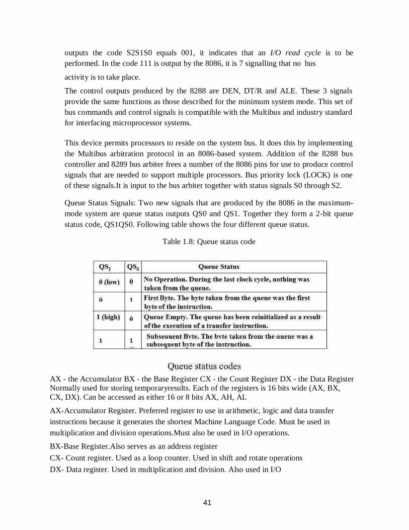
Queue Status Signals: Two new signals that are produced by the 8086 in the maximum-
mode system are queue status outputs QS0 and QS1. Together they form a 2-bit queue
status code, QS1QS0. Following table shows the four different queue status.
Table 1.8: Queue status code
AX - the Accumulator BX - the Base Register CX - the Count Register DX - the Data Register Normally used for storing temporaryresults. Each of the registers is 16 bits wide (AX, BX,
CX, DX). Can be accessed as either 16 or 8 bits AX, AH, AL
AX-Accumulator Register. Preferred register to use in arithmetic, logic and data transfer
instructions because it generates the shortest Machine Language Code. Must be used in
multiplication and division operations.Must also be used in I/O operations.
BX-Base Register.Also serves as an address register
CX- Count register. Used as a loop counter. Used in shift and rotate operations
DX- Data register. Used in multiplication and division. Also used in I/O
42
operations
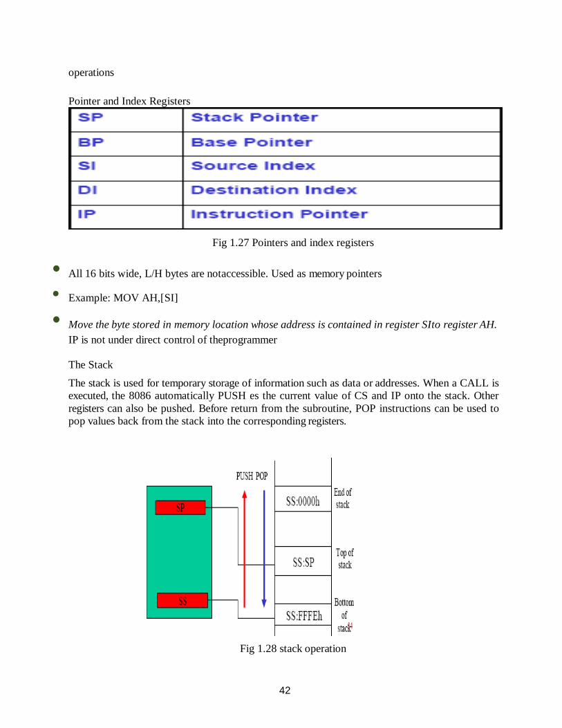
Pointer and Index Registers
Fig 1.27 Pointers and index registers
• All 16 bits wide, L/H bytes are notaccessible. Used as memory pointers
• Example: MOV AH,[SI]
• Move the byte stored in memory location whose address is contained in register SIto register AH.
IP is not under direct control of theprogrammer
The Stack
The stack is used for temporary storage of information such as data or addresses. When a CALL is
executed, the 8086 automatically PUSH es the current value of CS and IP onto the stack. Other
registers can also be pushed. Before return from the subroutine, POP instructions can be used to
pop values back from the stack into the corresponding registers.
Fig 1.28 stack operation

43
Test signals in 8086
TEST is an input pin and is only used by the wait instruction .the 8086 enter a wait state after execution of the wait instruction until a low is Seen on the test pin. Used in conjunction with the WAIT instruction in multiprocessing environments. This is input from the 8087 coprocessor. During execution of a wait instruction, the CPU checks this signal. If it is low, execution of the signal will continue; if not, it will stop executing. Coprocessor Execution
Fig 1.29. Coprocessor
execution
Multiprocessor
configuration Advantages
High system throughput can be achieved by having more than one CPU. The system can be expanded in modular form. Each bus master module is an independent unit and normally resides on a separate PC board. One can be added or removed without affecting the others in the system. A failure in one module normally does not affect the breakdown of the entire system and the faulty module can be easily detected and replaced. Each bus master has its own local bus to access dedicated memory or IO devices. So a greater degree of parallel processing can be achieved.
44
Question Bank
Part A 1. Define microprocessor 2. In how many groups can the signals of 8085 be classified? 3. What is the technology used in the manufacture of 8085? 4. Draw the block diagram of the built-in clock generator of 8085
5. What is the purpose of CLK signal of 8085? 6. What are the widths of data bus (DB) and address bus (AB) of 8085?
7. The address capability of 8085 is 64 KB. Explain. 8. Does 8085 have serial I/O control 9. What jobs ALU of 8085 can perform?
10. How many hardware interrupts 8085 supports?
11. How many I/O ports can 8085 access?
12. Why the lower byte address bus (A0 – A7) and data bus (D0 – D7) are multiplexed?
13. Why the lower byte address bus (A0 – A7) and data bus (D0 – D7) are multiplexed? 14. List the interrupts of 8085
15. List the flag bits of 8086
PART B 1. Explain the architecture of 8085 2. Discuss the addressing modes of 8085 3. Draw the timing diagram for the given instructions
a. STA b. CALL c. LDA d. MOV A,M
4. Explain the 8086 architecture with neat diagram 5. Explain the interrupts of 8085
TEXT / REFERENCE BOOKS
1. Ramesh Gaonkar, ―Microprocessor Architecture, Programming and applications with
8085‖, 5th Edition,
Penram International Publishing Pvt Ltd, 2010.
2. Kenneth J Ayala, ―The 8051 Microcontroller‖, 2nd Edition, Thomson, 2005.
3. Nagoor Kani A, ―Microprocessor and Microcontroller‖, 2nd Edition, Tata McGraw Hill, 2012.
4. Mathur A.P. ‖ Introduction to microprocessor .―
5. Muhammad Ali Mazidi.‖The 8051 Microcontroller and Embedded Systems.‖
45
UNIT – II– MICROPROCESSORS AND MICROCONTROLLERS– SECA 1601
SCHOOL OF ELECTRICAL AND ELECTRONICS
DEPARTMENT OF ELECTRONICS AND COMMUNICATION ENGINEERING
46
UNIT 2 PROGRAMMING 8085 MICROPROCESSOR
8085 assembly language programming, addressing modes, 8085 instruction set, Instruction formats,
Instruction Classification: data transfer, arithmetic operations, logical operations, branching
operations, machine control —Stack and subroutines, Example Programs
1.Instruction Set of 8085
An instruction is a binary pattern designed inside a microprocessor to perform a specific
function.
The entire group of instructions that a microprocessor supports is called Instruction Set.
8085 has 246 instructions.
Each instruction is represented by an 8-bit binary value.
These 8-bits of binary value is called Op-Code or Instruction Byte.
Classification of Instruction Set
• Data Transfer Instruction
• Arithmetic Instructions
• Logical Instructions
• Branching Instructions
• Control Instructions
Data Transfer Instructions • These instructions move data between registers, or between memory and
registers. • These instructions copy data from source to destination. • While copying, the contents of
source are not modified.
Arithmetic Instructions • These instructions perform the operations like: • Addition • Subtract •
Increment • Decrement
Logical Instructions • These instructions perform logical operations on data stored in registers,
memory and status flags. • The logical operations are: • AND • OR • XOR • Rotate • Compare
• Complement
Branching Instructions • The branching instruction alter the normal sequential flow. • These
instructions alter either unconditionally or conditionally
Control Instructions • The control instructions control the operation of microprocessor.
DATA TRANSFER INSTRUCTIONS
Copy of data
MOV Moves data from register to register / memory
MVI Moves immediate data to register /
memory Load Instructions
LDA Load accumulator direct
LDAX Load accumulator indirect
LHLD Load H&L registers direct
LXI Load register pair
immediate Store Instructions
STA Store accumulator direct
SPHL Copy H&L registers to stack pointer.
STAX Store accumulator indirect

47
Opcode Operand Meaning Explanation
MOV
Rd, Sc
M, Sc Dt, M
Copy from the
source (Sc) to the
destination(Dt)
This instruction copies the
contents of the source register
into the destination register
without any alteration.
Example − MOV A, L
MVI
Rd, data
M, data
Move immediate 8-bit
The 8-bit data is stored in the
destination register or memory.
Example − MVI H, 55H
LDA
16-bit address
Load the accumulator
The contents of a memory
location, specified by a 16-bit
address in the operand, are copied
to the accumulator.
Example − LDA 2034H
LDAX
B/D Reg. pair
Load the
accumulat
or indirect
The contents of the designated
register pair point to a memory
location. This instruction copies
the contents of that memory
location into the accumulator.
Example − LDAX B
LXI
Reg. pair, 16-
bit data
Load the
register pair immediate
The instruction loads 16-bit data
in the register pair designated in
the register or the memory.
Example − LXI H, 3225H
LHLD
16-bit address
Load H and L
registers direct
The instruction copies the
contents of the memory location
pointed out by the address into
register L and copies the contents
of the next memory location into
register H.

48
Example − LHLD 3225H
STA
16-bit address
16-bit address
The contents of the accumulator
are copied into the memory
location specified by the operand.
This is a 3-byte instruction, the
second byte specifies the low-
order address and the third byte
specifies the high-order address.
Example − STA 3257H
STAX
16-bit address
Store the accumulator
indirect
The contents of the accumulator
are copied into the memory
location specified by the contents
of the operand.
Example − STAX D
SHLD
16-bit address
Store H and L registers
direct
The contents of register L are
stored in the memory location
specified by the 16-bit address in
the operand and the contents of H
register are stored into the next
memory location by incrementing
the operand.
This is a 3-byte instruction, the
second byte specifies the low-
order address and the third byte
specifies the high-order address.
Example − SHLD 3225H
XCHG
None
Exchange H and L with D and
E
The contents of register H are
exchanged with the contents of
register D, and the contents of
register L are exchanged with the
contents of register E.
Example − XCHG

SPHL
None
Copy H and L registers to the
stack pointer
The instruction loads the contents
of the H and L registers into the
stack pointer register. The
contents of the H register provide
the high-order address and the
contents of the L register provide
the low-order address.
Example − SPHL
XTHL
None
Exchange H and L with top of
stack
The contents of the L register are
exchanged with the stack location
pointed out by the contents of the
stack pointer register.
The contents of the H register are
exchanged with the next stack
location (SP+1).
Example − XTHL
PUSH
Reg. pair
Push the register pair onto
the stack
The contents of the register pair
designated in the operand are
copied onto the stack in the
following sequence.
The stack pointer register is
decremented and the contents of
the high order register (B, D, H,
A) are copied into that location.
The stack pointer register is
decremented again and the
contents of the low-order register
(C, E, L, flags) are copied to that
location.
Example − PUSH PSW
POP
Reg. pair
Pop off stack to the
register pair
45
The contents of the memory
location pointed out by the stack
pointer register are copied to the
low-order register (C, E, L, status
flags) of the operand.

46
The stack pointer is incremented
by 1 and the contents of that
memory location are copied to the
high- order register (B, D, H, A) of
the operand.
The stack pointer register is again
incremented by 1.
Example – POP D
OUT
8-bit port
address
Output the data from the
accumulator to a port with
8bit address
The contents of the accumulator
are copied into the I/O port
specified by the operand.
Example − OUT 12H
IN
8-bit port
address
Input data to accumulator
from a port with 8-bit
address
The contents of the input port
designated in the operand are read
and loaded into the accumulator.
Example – IN 55H
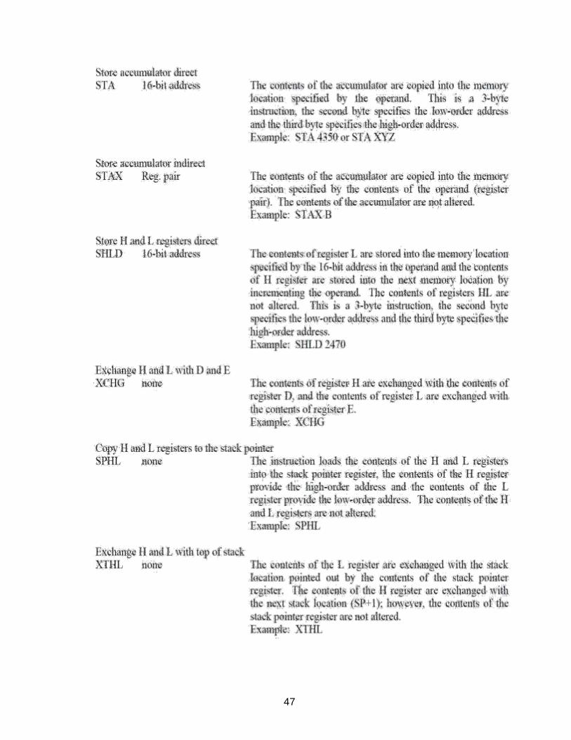
47
48
Arithmetic Instructions:
49
50

51
52
53

54
55
84
QUESTION BANK
PART A
1. Identify the addressing modes of LDA and LDAXB instruction
2. Identify the no of bytes of XTHL and LXI H,16bit
3. Define addressing modes
4. Classify the instruction sets of 8085
5. Explain SPHL instruction with example
6. What is the difference between CMP and SUB instruction
7. When the parity flag will set
8. What determines the number of bytes to be fetched from memory to execute an instruction?
9. What are the different instruction word sizes in 8085?
10. Give one example each of 1-byte, 2-byte and 3-byte instructions.
11. Mention the different types of operations possible with arithmetic, logical,branch and machine
control operations
12. What is an instruction?
13. What are the different types of data transfer operations possible?
14. What is the output in 9100 after executing the following instructions MVI A, 09
MVI B, 04 ADD B DAA
STA 9100 HLT
15. What is the content in DE register? MVI A,09
ADI 77 PUSH PSW POP D HLT
PART B
1. Classify the instruction set based on the operations performed and explain with examples
2. Classify the instruction set based on the size of the instructions and explain with examples
3. Explain a. XTHL b.SPHL c.PCHL d.RAR e.SIM
4. Explain with example a.LDAX B b.PUSH PSW c.RLC d.JNC 16bit e.XRA A
5. Write an ALP to sort a given array in ascending order
6. Write an ALP to find a factorial of a number
7. Write an ALP to add two multibyte data
8. Write an ALP to generate fibonocci series Note: Study all the programs
85
TEXT / REFERENCE BOOKS
1. Ramesh Gaonkar, ―Microprocessor Architecture, Programming and applications with 8085‖, 5th Edition,
Penram International Publishing Pvt Ltd, 2010.
2. Kenneth J Ayala, ―The 8051 Microcontroller‖, 2nd Edition, Thomson, 2005.
3. Nagoor Kani A, ―Microprocessor and Microcontroller‖, 2nd Edition, Tata McGraw Hill, 2012.
4. Mathur A.P. ‖ Introduction to microprocessor .―
5. Muhammad Ali Mazidi.‖The 8051 Microcontroller and Embedded Systems.‖

86
UNIT – III– MICROPROCESSORS AND MICROCONTROLLERS– SECA 1601
SCHOOL OF ELECTRICAL AND ELECTRONICS
DEPARTMENT OF ELECTRONICS AND COMMUNICATION ENGINEERING
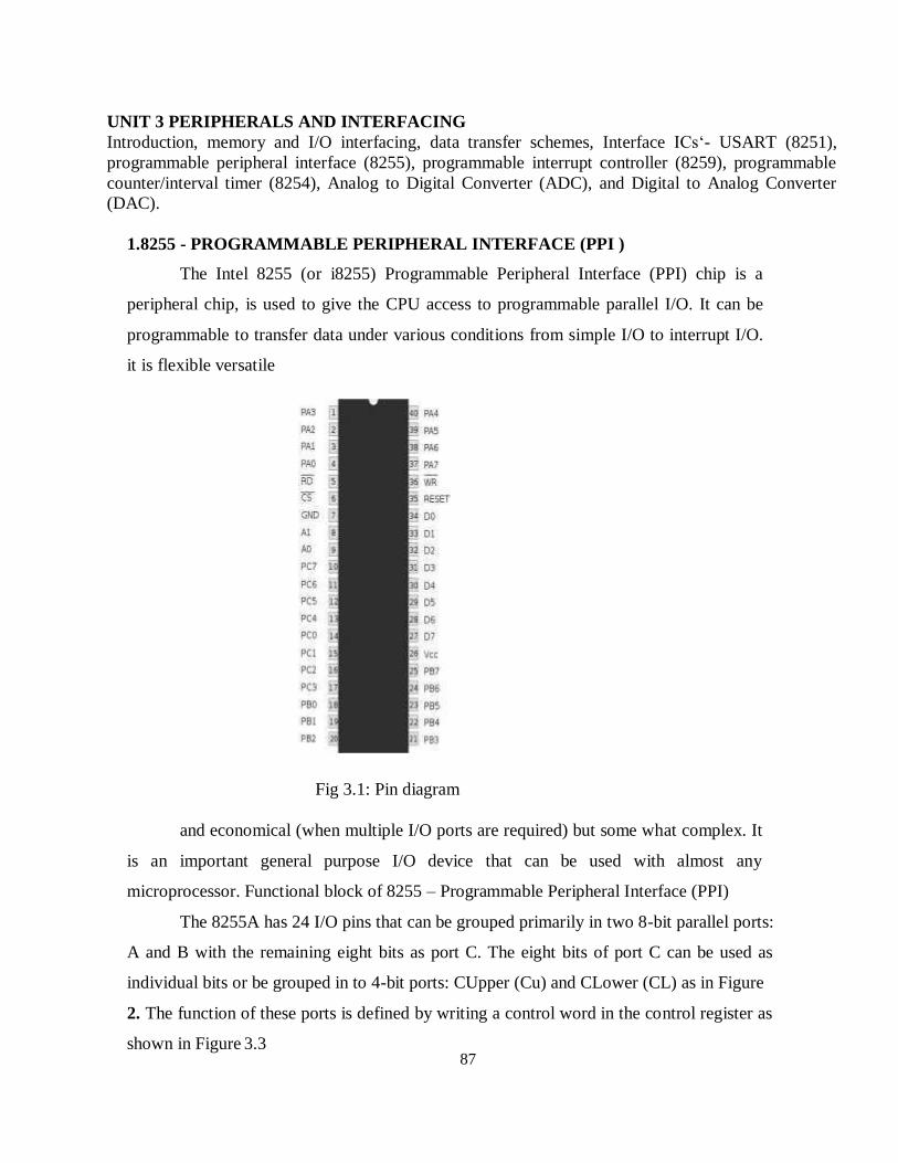
87
UNIT 3 PERIPHERALS AND INTERFACING
Introduction, memory and I/O interfacing, data transfer schemes, Interface ICs‘- USART (8251),
programmable peripheral interface (8255), programmable interrupt controller (8259), programmable
counter/interval timer (8254), Analog to Digital Converter (ADC), and Digital to Analog Converter
(DAC).
1.8255 - PROGRAMMABLE PERIPHERAL INTERFACE (PPI )
The Intel 8255 (or i8255) Programmable Peripheral Interface (PPI) chip is a
peripheral chip, is used to give the CPU access to programmable parallel I/O. It can be
programmable to transfer data under various conditions from simple I/O to interrupt I/O.
it is flexible versatile
Fig 3.1: Pin diagram
and economical (when multiple I/O ports are required) but some what complex. It
is an important general purpose I/O device that can be used with almost any
microprocessor. Functional block of 8255 – Programmable Peripheral Interface (PPI)
The 8255A has 24 I/O pins that can be grouped primarily in two 8-bit parallel ports:
A and B with the remaining eight bits as port C. The eight bits of port C can be used as
individual bits or be grouped in to 4-bit ports: CUpper (Cu) and CLower (CL) as in Figure
2. The function of these ports is defined by writing a control word in the control register as
shown in Figure 3.3
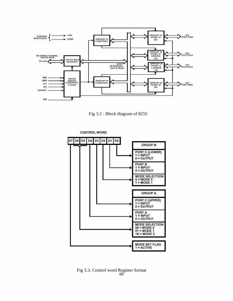
88
Fig 3.2 : Block diagram of 8255
Fig 3.3. Control word Register format

89
Data Bus Buffer
This three-state bi-directional 8-bit buffer is used to interface the 8255 to the system data
bus. Data is transmitted or received by the buffer upon execution of input or output
instructions by theCPU. Control words and status information are also transferred through
the data bus buffer.Read/Write and Control Logic
The function of this block is to manage all of the internal and external transfers of both Data
and Control or Status words. It accepts inputs from the CPU Address and Control busses
and in turn, issues commands to both of the Control Groups.
(CS) Chip Select. A "low" on this input pin enables the communication between the 8255
and the CPU.
(RD) Read. A "low" on this input pin enables 8255 to send the data or status information to
the CPU on the data bus. In essence, it allows the CPU to "read from" the 8255.
(WR) Write. A "low" on this input pin enables the CPU to write data or control words into
the 8255.
(A0 and A1) Port Select 0 and Port Select 1. These input signals, in conjunction with the
RD andWR inputs, control the selection of one of the three ports or the control word
register. They are normally connected to the least significant bits of the address bus (A0
and A1).
Fig 3.4 selection of Ports and Control reg

90
(RESET) Reset. A "high" on this input initializes the control register to 9Bh and all ports
(A, B,C) are set to the input mode.
Group A and Group B Controls
The functional configuration of each port is programmed by the systems software. In
essence, theCPU "outputs" a control word to the 8255. The control word contains
information such as "mode", "bit set", "bit reset", etc., that initializes the functional
configuration of the 8255. Eachof the Control blocks (Group A and Group B) accepts
"commands" from the Read/Write Control logic, receives "control words" from the internal
data bus and issues the proper commands to its associated ports.
Ports A, B, and C
The 8255 contains three 8-bit ports (A, B, and C). All can be configured to a wide variety
of functional characteristics by the system software but each has its own special features or
"personality" to further enhance
e the power and flexibility of the 8255.
Port A One 8-bit data output latch/buffer and one 8-bit data input latch. Both "pull-up" and
"pull- down" bus-hold devices are present on Port A.
Port B One 8-bit data input/output latch/buffer and one 8-bit data input buffer.
Port C One 8-bit data output latch/buffer and one 8-bit data input buffer (no latch for input).
This port can be divided into two 4-bit ports under the mode control. Each 4-bit port contains
a 4-bit latch and it can be used for the control signal output and status signal inputs in
conjunction with ports A and B.
I. Operational modes of 8255
There are two basic operational modes of 8255:
1. Bit set/reset Mode (BSR Mode).
2. Input/Output Mode (I/O Mode).
The two modes are selected on the basis of the value present at the D7 bit of the Control Word

91
Register. When D7 = 1, 8255 operates in I/O mode and when D7 = 0, it operates in the
BSR mode.
1. Bit set/reset (BSR) mode
The Bit Set/Reset (BSR) mode is applicable to port C only. Each line of port C (PC0 -
PC7) can be set/reset by suitably loading the control word register as shown in Figure 4.
BSR mode and I/O mode are independent and selection of BSR mode does not affect the
operation of other portsin I/O mode.
Fig 3.5: 8255 Control register format for BSR mode
D7 bit is always 0 for BSR
mode. Bits D6, D5 and D4
are don't care bits.
Bits D3, D2 and D1 are used to select the pin of
Port C.Bit D0 is used to set/reset the selected pin
of Port C.
Selection of port C pin is determined as follows:

92
As an example, if it is needed that PC5 be set, then in the control word,
1. Since it is BSR mode, D7 = '0'.
2. Since D4, D5, D6 are not used, assume them to be'0'.
3. PC5 has to be selected, hence, D3 = '1', D2 = '0', D1 = '1'.
4. PC5 has to be set, hence, D0 = '1'.
Thus, as per the above values, 0B (Hex) will be loaded into the Control Word Register (CWR).
D7 D6 D5 D4 D3 D2 D1 D0
0 0 0 0 1 0 1 1
2. Input/Output mode
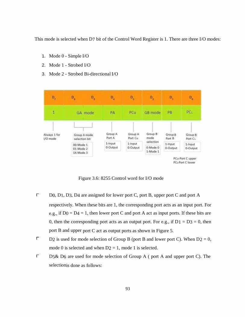
93
This mode is selected when D7 bit of the Control Word Register is 1. There are three I/O modes:
1. Mode 0 - Simple I/O
2. Mode 1 - Strobed I/O
3. Mode 2 - Strobed Bi-directional I/O
Figure 3.6: 8255 Control word for I/O mode
D0, D1, D3, D4 are assigned for lower port C, port B, upper port C and port A
respectively. When these bits are 1, the corresponding port acts as an input port. For
e.g., if D0 = D4 = 1, then lower port C and port A act as input ports. If these bits are
0, then the corresponding port acts as an output port. For e.g., if D1 = D3 = 0, then
port B and upper port C act as output ports as shown in Figure 5.
D2 is used for mode selection of Group B (port B and lower port C). When D2 = 0,
mode 0 is selected and when D2 = 1, mode 1 is selected.
D5& D6 are used for mode selection of Group A ( port A and upper port C). The
selectionis done as follows:
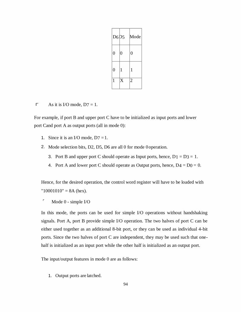
94
D6
D5
Mode
0
0
0
0
1
1
1 X 2
As it is I/O mode, D7 = 1.
For example, if port B and upper port C have to be initialized as input ports and lower
port Cand port A as output ports (all in mode 0):
1. Since it is an I/O mode, D7 = 1.
2. Mode selection bits, D2, D5, D6 are all 0 for mode 0 operation.
3. Port B and upper port C should operate as Input ports, hence, D1 = D3 = 1.
4. Port A and lower port C should operate as Output ports, hence, D4 = D0 = 0.
Hence, for the desired operation, the control word register will have to be loaded with
"10001010" = 8A (hex).
Mode 0 - simple I/O
In this mode, the ports can be used for simple I/O operations without handshaking
signals. Port A, port B provide simple I/O operation. The two halves of port C can be
either used together as an additional 8-bit port, or they can be used as individual 4-bit
ports. Since the two halves of port C are independent, they may be used such that one-
half is initialized as an input port while the other half is initialized as an output port.
The input/output features in mode 0 are as follows:
1. Output ports are latched.

95
2. Input ports are buffered, not latched.
3. Ports do not have handshake or interrupt capability.
4. With 4 ports, 16 different combinations of I/O are possible.
Mode 0 – input mode
In the input mode, the 8255 gets data from the external peripheral ports and the
CPUreads the received data via its data bus.
The CPU first selects the 8255 chip by making CS low. Then it selects
the desiredport using A0 and A1 lines.
The CPU then issues an RD signal to read the data from the
external peripheraldevice via the system data bus.
Mode 0 - output mode
In the output mode, the CPU sends data to 8255 via system data bus and then
the external peripheral ports receive this data via 8255 port.
CPU first selects the 8255 chip by making CS low. It then selects the desired
port using A0 and A1 lines.
CPU then issues a WR signal to write data to the selected port via the system
databus. This data is then received by the external peripheral device connected
to the selected port.
Mode 1
When we wish to use port A or port B for handshake (strobed) input or output operation,
we initialise that port in mode 1 (port A and port B can be initilalised to operate in
different modes, i.e., for e.g., port A can operate in mode 0 and port B in mode 1).
Some of the pins of port C function as handshake lines.
For port B in this mode (irrespective of whether is acting as an input port or output port),
PC0, PC1 and PC2 pins function as handshake lines.
96
If port A is initialised as mode 1 input port, then, PC3, PC4 and PC5 function
as handshake signals. Pins PC6 and PC7 are available for use as input/output
lines.
The mode 1 which supports handshaking has following features:
1. Two ports i.e. port A and B can be used as 8-bit i/o ports.
2. Each port uses three lines of port c as handshake signal and remaining two
signals can be used as i/o ports.
3. Interrupt logic is supported.
4. Input and Output data are latched.
Input Handshaking signals
1. IBF (Input Buffer Full) - It is an output indicating that the input latch
contains information.
2. STB (Strobed Input) - The strobe input loads data into the port latch, which
holds the information until it is input to the microprocessor via the IN
instruction.
3. INTR (Interrupt request) - It is an output that requests an interrupt. The
INTR pin becomes a logic 1 when the STB input returns to a logic 1, and is
cleared when the data are input from the port by the microprocessor.
4. INTE (Interrupt enable) - It is neither an input nor an output; it is an internal
bit programmed via the port PC4(port A) or PC2(port B) bit position.
Output Handshaking signals
1. OBF (Output Buffer Full) - It is an output that goes low whenever data are
output(OUT) to the port A or port B latch. This signal is set to a logic 1
whenever the ACK pulse returns from the external device.
97
2. ACK (Acknowledge)-It causes the OBF pin to return to a logic 1 level. The
ACK signal is a response from an external device, indicating that it has received
the data from the 82C55 port.
3. INTR (Interrupt request) - It is a signal that often interrupts the microprocessor
when the external device receives the data via the signal. this pin is qualified by
the internal INTE(interrupt enable) bit.
4. INTE (Interrupt enable) - It is neither an input nor an output; it is an internal
bit programmed to enable or disable the INTR pin. The INTE A bit is
programmed using the PC6 bit and INTE B is programmed using the PC2 bit.
Mode 2
Only group A can be initialized in this mode. Port A can be used for bidirectional
handshake data transfer. This means that data can be input or output on the same eight
lines (PA0 - PA7). Pins PC3 - PC7 are used as handshake lines for port A. The
remaining pins of port C (PC0 - PC2) can be used as input/output lines if group B is
initialized in mode 0 or as handshaking for port B if group B is initialized in mode 1. In
this mode, the 8255 may be used to extend the system bus to a slave microprocessor or
to transfer data bytes to and froma floppy disk controller. Acknowledgement and
handshaking signals are provided to maintain proper data flow and synchronisation
between the data transmitter and receiver.

98
II. Interfacing 8255 with 8085 processor
Fig 3.7. Interfacing 8255 with 8085 processor
The 8255 can be either memory mapped or I/O mapped in the system. In
the schematic shown in above is I/O mapped in the system.
Using a 3-to-8decoder generates the chip select signals for I/O mapped devices.
The address lines A4, A5 and A6 are decoded to generate eight chip select
signals (IOCS-0 to IOCS-7) and in this, the chip select IOCS- 1 is used to select
8255 as shown in Figure 3.7.
The address line A7 and the control signal IO/M (low) are used as enable for
thedecoder.
The address line A0 of 8085 is connected to A0 of 8255 and A1 of 8085 is
connected toA1 of 8255 to provide the internal addresses.
The data lines D0-D7 are connected to D0-D7 of the processor to achieve parallel
datatransfer.
The I/O addresses allotted to the internal devices of 8255 are listed in table.
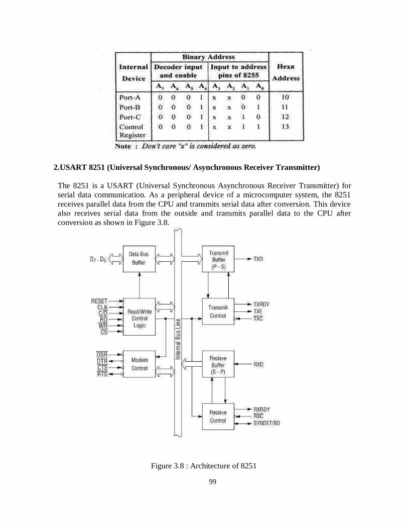
99
2.USART 8251 (Universal Synchronous/ Asynchronous Receiver Transmitter)
The 8251 is a USART (Universal Synchronous Asynchronous Receiver Transmitter) for
serial data communication. As a peripheral device of a microcomputer system, the 8251
receives parallel data from the CPU and transmits serial data after conversion. This device
also receives serial data from the outside and transmits parallel data to the CPU after
conversion as shown in Figure 3.8.
Figure 3.8 : Architecture of 8251
100
Transmitter Section
The transmitter section consists of three blocks—transmitter buffer register, output register
and the transmitter control logic block. The CPU deposits (when TXRDY = 1, meaning
that the transmitter buffer register is empty) data into the transmitter buffer register, which
is subsequently put into the output register (when TXE = 1, meaning that the output buffer
is empty). In the output register, the eight bit data is converted into serial form and comes
out
via TXD pin. The serial data bits are preceded by START bit and succeeded by STOP bit,
which are known as framing bits. But this happens only if transmitter is enabled and the
CTS is low. TXC signal is the transmitter clock signal which controls the bit rate on the
TXD line (output line). This clock frequency can be 1, 16 or 64 times the baud.
Receiver Section
The receiver section consists of three blocks — receiver buffer register, input register and
the receiver control logic block. Serial data from outside world is delivered to the input
register via RXD line, which is subsequently put into parallel form and placed in the receiver
buffer register. When this register is full, the RXRDY (receiver ready) line becomes high.
This line is then used either to interrupt the MPU or to indicate its own status. MPU then
accepts the data from the register. RXC line stands for receiver clock. This clock signal
controls the rate at which bits are received by the input register. The clock can be set to 1,
16 or 64 times the baud in the asynchronous mode.

101
Fig 3.9 : Pin Configuration of 8251
Pin Configuration of 8251 is shown in figure
11. D 0 to D 7 (l/O terminal)
This is bidirectional data bus which receive control words and transmits data from the
CPU andsends status words and received data to CPU.
RESET (Input terminal)
A "High" on this input forces the 8251 into "reset status." The device waits for the
writing of"mode instruction." The min. reset width is six clock inputs during the operating
status of CLK.
CLK (Input terminal)
CLK signal is used to generate internal device timing. CLK signal is independent of RXC
or TXC. However, the frequency of CLK must be greater than 30 times the RXC and TXC
at Synchronous mode and Asynchronous "x1" mode, and must be greater than 5 times at
Asynchronous "x16" and "x64" mode.
102
WR (Input terminal)
This is the "active low" input terminal which receives a signal for writing transmit
data andcontrol words from the CPU into the 8251.
RD (Input terminal)
This is the "active low" input terminal which receives a signal for reading receive data and
statuswords from the 8251.
C/D (Input terminal)
This is an input terminal which receives a signal for selecting data or command words and
statuswords when the 8251 is accessed by the CPU. If C/D = low, data will be accessed. If
C/D
= high, command word or status word will
be accessed.CS (Input terminal)
This is the "active low" input terminal which selects the 8251 at low level when the CPU
accesses. Note: The device won‘t be in "standby status"; only setting CS =
High. TXD (output terminal)
This is an output terminal for transmitting data from which serial-converted data is sent out.
The device is in "mark status" (high level) after resetting or during a status when transmit is
disabled. It is also possible to set the device in "break status" (low level) by a command.
TXRDY (output terminal)
This is an output terminal which indicates that the 8251is ready to accept a transmitted data
character. But the terminal is always at low level if CTS = high or the device was set in
"TX disable status" by a command. Note: TXRDY status word indicates that transmit data
character isreceivable, regardless of CTS or command. If the CPU writes a data character,
TXRDY will be reset by the leading edge or WR signal.
TXEMPTY (Output terminal)
This is an output terminal which indicates that the 8251 has transmitted all the characters
and hadno data character. In "synchronous mode," the terminal is at high level, if transmit
data charactersare no longer remaining and sync characters are automatically transmitted.

103
If the CPU writes a data character, TXEMPTY will be reset by the leading edge of WR
signal. Note : As the transmitter is disabled by setting CTS "High" or command, data written
before disable will be sent out. Then TXD and TXEMPTY will be "High". Even if a data is
written after disable, that data is not sent out and TXE will be "High". After the transmitter
is enabled, it sent out. (Refer to Timing Chart of Transmitter Control and Flag Timing)
TXC (Input terminal)
This is a clock input signal which determines the transfer speed of transmitted data. In
"synchronous mode," the baud rate will be the same as the frequency of TXC. In
"asynchronous mode", it is possible to select the baud rate factor by mode instruction. It can
be 1, 1/16 or 1/64 the TXC. The falling edge of TXC sifts the serial data out of the 8251.
RXD (input terminal)
This is a terminal which receives
serial data.RXRDY (Output
terminal)
This is a terminal which indicates that the 8251 contains a character that is ready to READ.
If theCPU reads a data character, RXRDY will be reset by the leading edge of RD signal.
\Unless the CPU reads a data character before the next one is received completely, the
preceding data will belost. In such a case, an overrun error flag status word will be set.
RXC (Input terminal)
This is a clock input signal which determines the transfer speed of received data. In
"synchronous mode," the baud rate is the same as the frequency of RXC. In "asynchronous
mode," it is possible to select the baud rate factor by mode instruction. It can be 1, 1/16,
1/64 the RXC.
SYNDET/BD (Input or output terminal)
This is a terminal whose function changes according to mode. In "internal synchronous
mode." this terminal is at high level, if sync characters are received and synchronized. If a
status word is read, the terminal will be reset. In "external synchronous mode, "this is an
input terminal. A "High" on this input forces the 8251 to start receiving data characters.
In "asynchronous mode," this is an output terminal which generates "high level"output
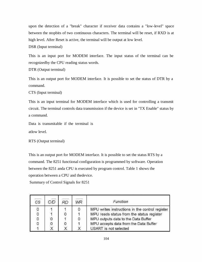
104
upon the detection of a "break" character if receiver data contains a "low-level" space
between the stopbits of two continuous characters. The terminal will be reset, if RXD is at
high level. After Reset is active, the terminal will be output at low level.
DSR (Input terminal)
This is an input port for MODEM interface. The input status of the terminal can be
recognizedby the CPU reading status words.
DTR (Output terminal)
This is an output port for MODEM interface. It is possible to set the status of DTR by a
command.
CTS (Input terminal)
This is an input terminal for MODEM interface which is used for controlling a transmit
circuit. The terminal controls data transmission if the device is set in "TX Enable" status by
a command.
Data is transmitable if the terminal is
atlow level.
RTS (Output terminal)
This is an output port for MODEM interface. It is possible to set the status RTS by a
command. The 8251 functional configuration is programmed by software. Operation
between the 8251 anda CPU is executed by program control. Table 1 shows the
operation between a CPU and thedevice.
Summary of Control Signals for 8251

105
Control Words
There are two types of control word.
1. Mode instruction (setting of function)
2. Command (setting of operation)
1) Mode Instruction
Mode instruction is used for setting the function of the 8251. Mode instruction will be in
"wait for write" at either internal reset or external reset. That is, the writing of a control
word after resetting will be recognized as a "mode instruction."
Items set by mode instruction are as follows:
Fig 3.10: Bit configuration of Mode instruction (Asynchronous)
• Synchronous/asynchronous mode
• Stop bit length (asynchronous mode)
• Character length
• Parity bit
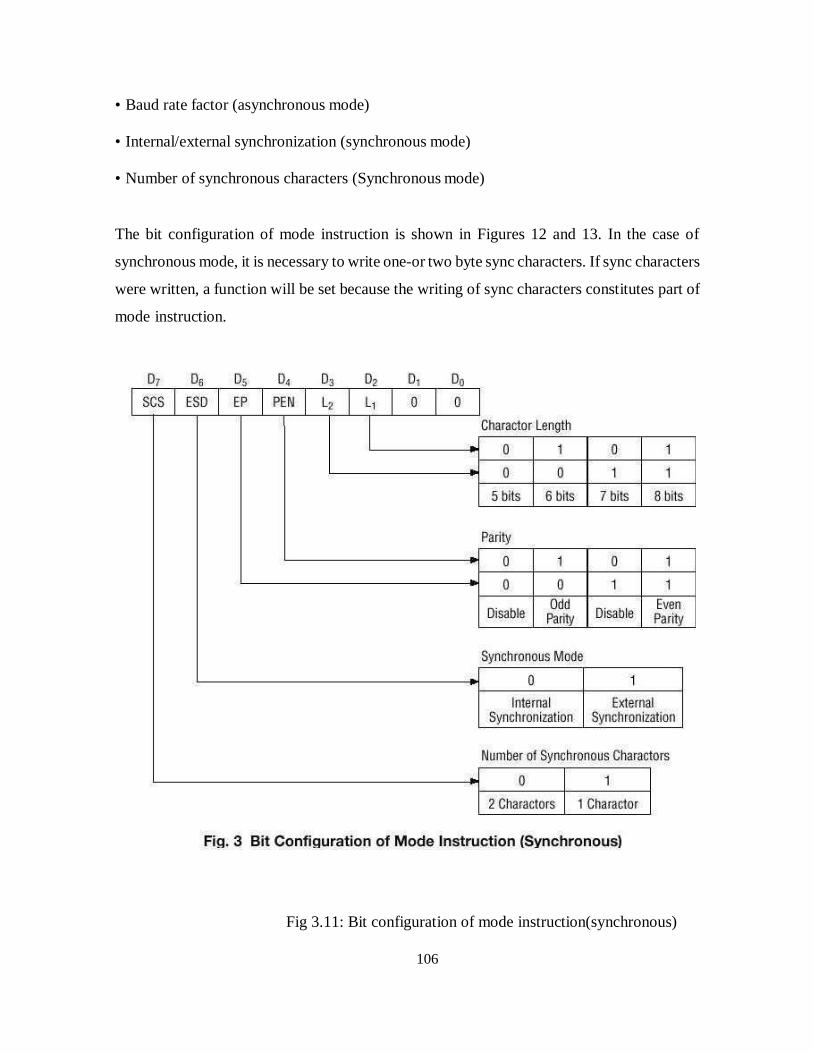
106
• Baud rate factor (asynchronous mode)
• Internal/external synchronization (synchronous mode)
• Number of synchronous characters (Synchronous mode)
The bit configuration of mode instruction is shown in Figures 12 and 13. In the case of
synchronous mode, it is necessary to write one-or two byte sync characters. If sync characters
were written, a function will be set because the writing of sync characters constitutes part of
mode instruction.
Fig 3.11: Bit configuration of mode instruction(synchronous)

107
2) Command
Command is used for setting the operation of the 8251. It is possible to write a
commandwhenever necessary after writing a mode instruction and sync characters as
shown in figure 14.
Items to be set by command are as follows:
• Transmit Enable/Disable
• Receive Enable/Disable
• DTR, RTS Output of data.
• Resetting of error flag.
• Sending to break characters
• Internal resetting
• Hunt mode (synchronous mode)

108
Fig 3.12: Bit configuration of command
Status Word
It is possible to see the internal status of the 8251 by reading a status word. The
bit configuration of status word is shown in Fig.15.
Fig 3.13: Bit configuration of Status Word
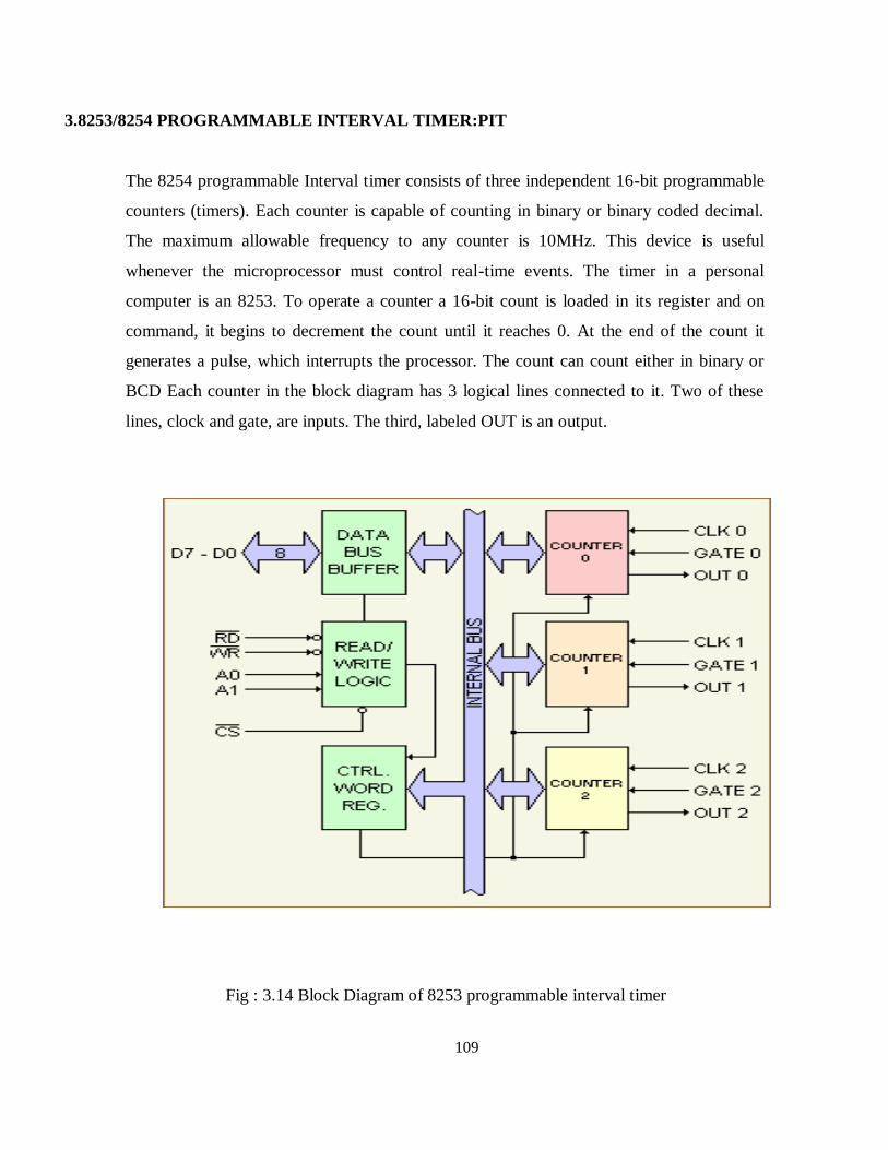
109
3.8253/8254 PROGRAMMABLE INTERVAL TIMER:PIT
The 8254 programmable Interval timer consists of three independent 16-bit programmable
counters (timers). Each counter is capable of counting in binary or binary coded decimal.
The maximum allowable frequency to any counter is 10MHz. This device is useful
whenever the microprocessor must control real-time events. The timer in a personal
computer is an 8253. To operate a counter a 16-bit count is loaded in its register and on
command, it begins to decrement the count until it reaches 0. At the end of the count it
generates a pulse, which interrupts the processor. The count can count either in binary or
BCD Each counter in the block diagram has 3 logical lines connected to it. Two of these
lines, clock and gate, are inputs. The third, labeled OUT is an output.
Fig : 3.14 Block Diagram of 8253 programmable interval timer
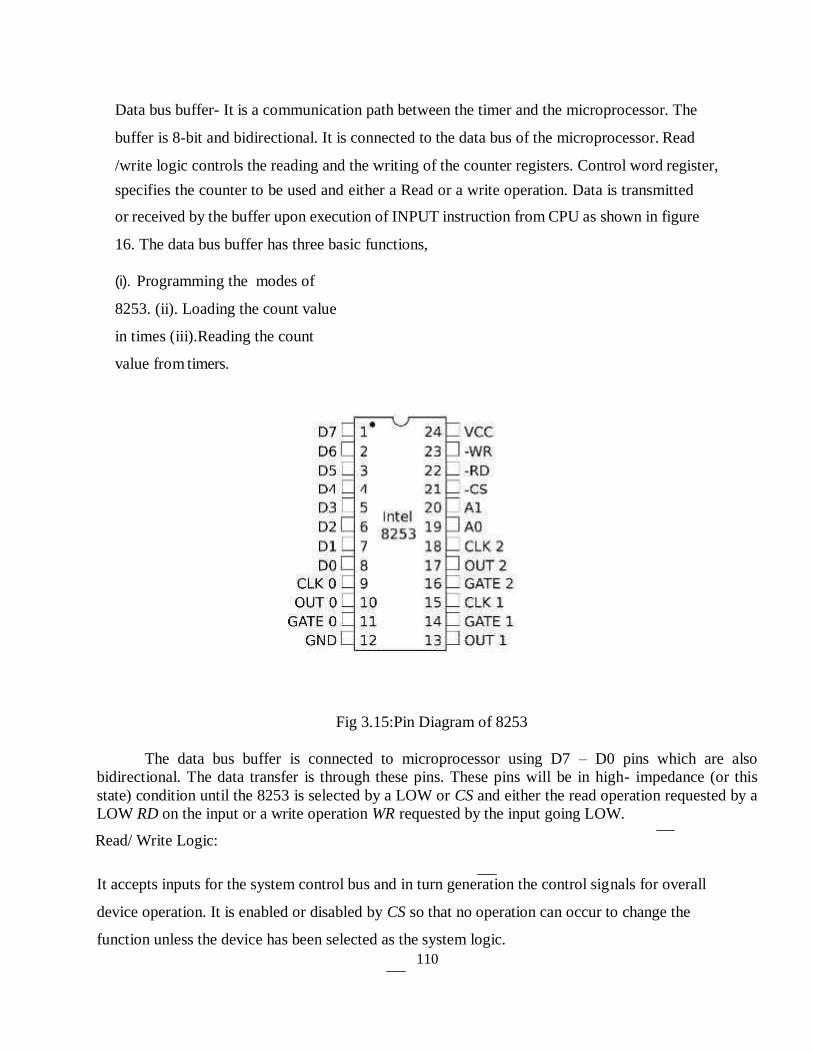
110
Data bus buffer- It is a communication path between the timer and the microprocessor. The
buffer is 8-bit and bidirectional. It is connected to the data bus of the microprocessor. Read
/write logic controls the reading and the writing of the counter registers. Control word register,
specifies the counter to be used and either a Read or a write operation. Data is transmitted
or received by the buffer upon execution of INPUT instruction from CPU as shown in figure
16. The data bus buffer has three basic functions,
(i). Programming the modes of
8253. (ii). Loading the count value
in times (iii).Reading the count
value from timers.
Fig 3.15:Pin Diagram of 8253
The data bus buffer is connected to microprocessor using D7 – D0 pins which are also
bidirectional. The data transfer is through these pins. These pins will be in high- impedance (or this
state) condition until the 8253 is selected by a LOW or CS and either the read operation requested by a
LOW RD on the input or a write operation WR requested by the input going LOW.
Read/ Write Logic:
It accepts inputs for the system control bus and in turn generation the control signals for overall
device operation. It is enabled or disabled by CS so that no operation can occur to change the
function unless the device has been selected as the system logic.

111
CS : The chip select input is used to enable the communicate between 8253 and themicroprocessor
by means of data bus. A low an CS enables the data bus buffers, while a high disable the buffer.
The CS input does not have any affect on the operation of threetimes once they have been
initialized. The normal configuration of a system employs an decode logic which actives CS line,
whenever a specific set of addresses thatcorrespond to 8253 appear on the address bus.
RD & WR :
The read ( RD ) and write WR pins central the direction of data transfer on the 8-bit bus.
Whenthe input RD pin is low. Then CPU is inputting data from 8253 in the form of counter
value. When WR pins is low, then CPU is sending data to 8253 in the form of mode
information or loading counters. The RD &WR should not both be
low simultaneously. When RD & WR pins are HIGH, the data bus buffer is disabled.
A0 & A1:
These two input lines allow the microprocessor to specify which one of the internal register
in the 8253 is going to be used for the data transfer. Fig shows how these two lines are
used to select either the control word register or one of the 16-bit counters.
112
Control word register:
It is selected when A0 and A1 . It the accepts information from the data bus buffer and
stores itin a register. The information stored in then register controls the operation mode of
each counter,selection of binary or BCD counting and the loading of each counting and the
loading of each count register. This register can be written into, no read operation of this
content is available.
Counters:
Each of the times has three pins associated with it. These are CLK (CLK) the gate (GATE)
and the output (OUT).
CLK:
This clock input pin provides 16-bit times with the signal to causes the times to decrement
maxm clock input is 2.6MHz. Note that the counters operate at the negative edge (H1 to L0) of
this
clock input. If the signal on this pin is generated by a fixed oscillator then the user has
implemented a standard timer. If the input signal is a string of randomly occurring pulses,
then it is called implementation of a counter.
GATE:
The gate input pin is used to initiate or enable counting. The exact effect of the gate signal
dependson which of the six modes of operation is chosen.
OUTPUT:
The output pin provides an output from the timer. It actual use depends on the mode of
operationof the timer. The counter can be read ―in the fly‖ without inhibiting gate pulse or
clock input.
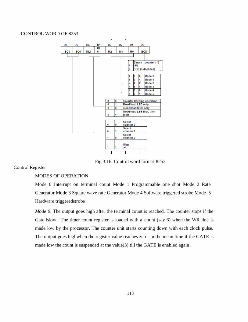
113
CONTROL WORD OF 8253
Fig 3.16: Control word format-8253
Control Register
MODES OF OPERATION
Mode 0 Interrupt on terminal count Mode 1 Programmable one shot Mode 2 Rate
Generator Mode 3 Square wave rate Generator Mode 4 Software triggered strobe Mode 5
Hardware triggeredstrobe
Mode 0: The output goes high after the terminal count is reached. The counter stops if the
Gate islow.. The timer count register is loaded with a count (say 6) when the WR line is
made low by the processor. The counter unit starts counting down with each clock pulse.
The output goes highwhen the register value reaches zero. In the mean time if the GATE is
made low the count is suspended at the value(3) till the GATE is enabled again .
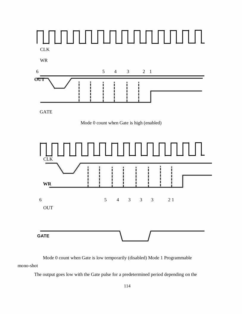
114
OUT
GATE
CLK
WR
6 5 4 3 2 1
GATE
Mode 0 count when Gate is high (enabled)
CLK
6 5 4 3 3 3 2 1
OUT
Mode 0 count when Gate is low temporarily (disabled) Mode 1 Programmable
mono-shot
The output goes low with the Gate pulse for a predetermined period depending on the
WR
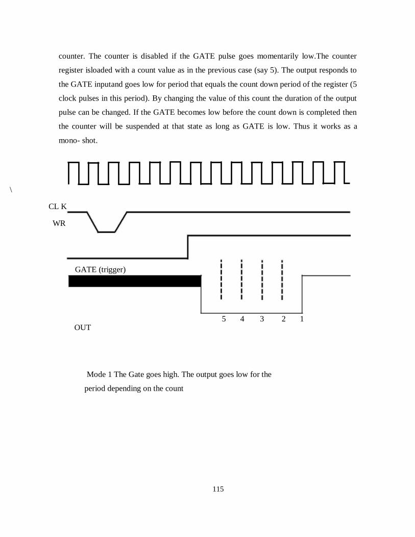
115
counter. The counter is disabled if the GATE pulse goes momentarily low.The counter
register isloaded with a count value as in the previous case (say 5). The output responds to
the GATE inputand goes low for period that equals the count down period of the register (5
clock pulses in this period). By changing the value of this count the duration of the output
pulse can be changed. If the GATE becomes low before the count down is completed then
the counter will be suspended at that state as long as GATE is low. Thus it works as a
mono- shot.
\
CL K
WR
GATE (trigger)
5 4 3 2 1 OUT
Mode 1 The Gate goes high. The output goes low for the
period depending on the count
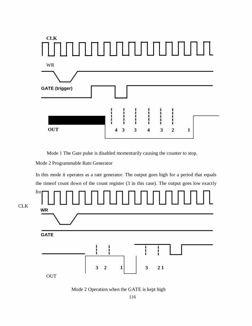
116
GATE (trigger)
CLK
WR
Mode 1 The Gate pulse is disabled momentarily causing the counter to stop.
Mode 2 Programmable Rate Generator
In this mode it operates as a rate generator. The output goes high for a period that equals
the timeof count down of the count register (3 in this case). The output goes low exactly
for one clock period before it becomes high again. This is a periodic operation.
CLK
OUT
Mode 2 Operation when the GATE is kept high
OUT 4 3 3 4 3 2 1
WR
GATE
3 2 1 3 2 1

117
WR
GATE
OUT 3 2 1 3 3 2 1 Mode 2 operation when the GATE isdisabled
WR
n=
4 OUT (n=4)
OUT (n=5)
CLK
momentarily.
Mode 3 Programmable Square Wave Rate Generator
It is similar to Mode 2 but the output high and low period is symmetrical. The output
goes high after the count is loaded and it remains high for period which equals the count
down period of the counter register. The output subsequently goes low for an equal period
and hence generates a symmetrical square wave unlike Mode 2. The GATE has no role here.
CLK
Mode3 Operation: Square Wave generator

118
WR
OUT
4 3 2 1
WR
GATE OUT
4 3 3 2 1
Mode 4 Software Triggered Strobe
In this mode after the count is loaded by the processor the count down starts. The output
goes low for one clock period after the count down is complete. The count down can be
suspended bymaking the GATE low . This is also called a software triggered strobe as the
count down is initiated by a program.
CLK
Mode 4 Software Triggered Strobe when GATE is high

119
WR
GATE
OUT
5 4 3 2 1
LK
Mode 4 Software Triggered Strobe when GATE is momentarily low
Mode 5 Hardware Triggered Strobe
The count is loaded by the processor but the count down is initiated by the GATE pulse. The
transition from low to high of the GATE pulse enables count down. The output goes low
for one clock period after the count down is complete.
CLK
Mode 5 Hardware Triggered Strobe
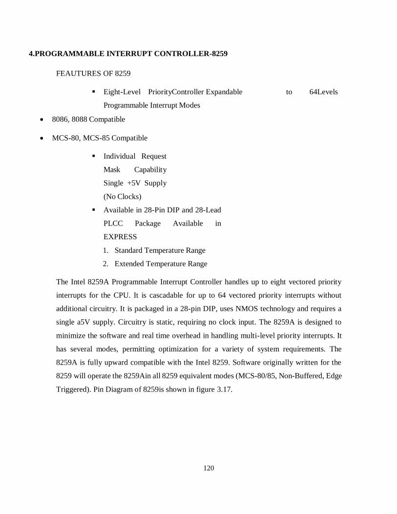
120
4.PROGRAMMABLE INTERRUPT CONTROLLER-8259
FEAUTURES OF 8259
Eight-Level PriorityController Expandable to 64Levels
Programmable Interrupt Modes
8086, 8088 Compatible
MCS-80, MCS-85 Compatible
Individual Request
Mask Capability
Single +5V Supply
(No Clocks)
Available in 28-Pin DIP and 28-Lead
PLCC Package Available in
EXPRESS
1. Standard Temperature Range
2. Extended Temperature Range
The Intel 8259A Programmable Interrupt Controller handles up to eight vectored priority
interrupts for the CPU. It is cascadable for up to 64 vectored priority interrupts without
additional circuitry. It is packaged in a 28-pin DIP, uses NMOS technology and requires a
single a5V supply. Circuitry is static, requiring no clock input. The 8259A is designed to
minimize the software and real time overhead in handling multi-level priority interrupts. It
has several modes, permitting optimization for a variety of system requirements. The
8259A is fully upward compatible with the Intel 8259. Software originally written for the
8259 will operate the 8259Ain all 8259 equivalent modes (MCS-80/85, Non-Buffered, Edge
Triggered). Pin Diagram of 8259is shown in figure 3.17.
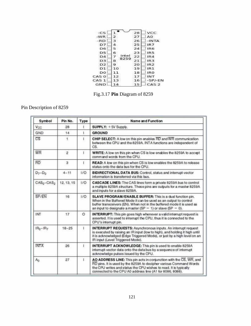
121
Fig.3.17 Pin Diagram of 8259
Pin Description of 8259

122
Fig. 3.18 Block Diagram of 8259
A more desirable method would be one that would allow the microprocessor to be
executing its main program and only stop to service peripheral devices when it is told to do
so bythe device itself. In effect, the method would provide an external asynchronous input
that would inform the processor that it should complete whatever instruction that is
currently being executedand fetch a new routine that will service the requesting device.
Once this servicing is complete, however, the processor would resume exactly where it left
off. This method is called Interrupt. It is easy to see that system throughput would drastically
increase, and thus more tasks could be assumed by the micro-computer to further enhance
its cost effectiveness. Block Diagram of 8259is shown in figure 18.
The Programmable Interrupt Controller (PIC) functions as an overall manager in an
Interrupt-Driven system environment. It accepts requests from the peripheral equipment,
determines which of the in-coming requests is of the highest importance (priori-ty),
123
ascertains whether the incoming request has a higher priority value than the level currently
being serviced, and issues an interrupt to the CPU based on this determination.
The 8259A is a device specifically designed for use in real time, interrupt driven
microcomputer systems. It manages eight levels or requests and has built-in features for
expandability to other 8259A's (up to 64 levels). It is programmed by the system's software
as an I/O peripheral. A selection of priority modes is available to the programmer so that the
manner in which the requests are processed by the 8259A can be configured to match his
system requirements. The priority modes can be changed or reconfigured dynamically at
any time during the main program. This means that the complete interrupt structure can be
defined as required, based on the total system environment.
5.Interrupt Request Register (Irr) And In-Service Register (Isr)
The interrupts at the IR input lines are handled by two registers in cascade, the
Interrupt Request Register (IRR) and the In-Service (ISR). The IRR is used to store all the
interrupt levels which are requesting service; and the ISR is used to store all the interrupt
levels which are being serviced.
PRIORITY RESOLVER
This logic block determines the priorites of the bits set in the IRR. The highest priority is
selected and strobed into the corresponding bit of the ISR during INTA pulse.
INTERRUPT MASK REGISTER (IMR)
The IMR stores the bits which mask the interrupt lines to be masked. The IMR operates on
the IRR. Masking of a higher priority input will not affect the interrupt request lines of lower
quality.
INT (INTERRUPT)
This output goes directly to the CPU interrupt input. The VOH level on this line is
designed to befully compatible with the 8080A, 8085A and 8086 input levels.
124
INTA (INTERRUPT ACKNOWLEDGE)
INTA pulses will cause the 8259A to release vectoring information onto the data bus. The
formatof this data depends on the system mode (mPM) of the 8259A.
DATA BUS BUFFER
This 3-state, bidirectional 8-bit buffer is used to inter-face the 8259A to the system Data
Bus. Control words and status information are transferred through the Data Bus Buffer.
READ/WRITE CONTROL LOGIC
The function of this block is to accept Output commands from the CPU. It contains the
Initialization Command Word (ICW) registers and Operation Command Word (OCW)
registers which store the various control formats for device operation. This function block
also allows the status of the 8259A to be transferred onto the Data Bus.
CS (CHIP SELECT)
A LOW on this input enables the 8259A. No reading or writing of the chip
willoccur unless the device is selected.
WR (WRITE)
A LOW on this input enables the CPU to write con-trol words (ICWs and OCWs)
to the8259A. RD (READ)
A LOW on this input enables the 8259A to send the status of the Interrupt Request
Register (IRR), In Service Register (ISR), the Interrupt Mask Register (IMR), or the
Interrupt level onto the Data Bus.

125
A0
This input signal is used in conjunction with WR and RD signals to write
commands into the various command registers, as well as reading the various status registers
of the chip. This line can be tied directly to one of the address lines.
INTERRUPT SEQUENCE
The powerful features of the 8259A in a microcomputer system are its programmability and
the interrupt routine addressing capability. The latter allows direct or indirect jumping to
the specificinterrupt routine requested without any polling of the interrupting devices. The
normal sequence of events during an interrupt depends on the type of CPU being used.
The events occur as follows in an MCS-80/85 sys-tem:
1. One or more of the INTERRUPT REQUEST lines (IR7±0) are raised high, setting
the correspond-ing IRR bit(s).
2. The 8259A evaluates these requests, and sends an INT to the CPU, if appropriate.
3. The CPU acknowledges the INT and responds with an INTA pulse.
4. Upon receiving an INTA from the CPU group, the highest priority ISR bit is set,
and the correspond-ing IRR bit is reset. The 8259A will also release a CALL
instruction code (11001101) onto the 8-bit Data Bus through its D7±0 pins.
5. This CALL instruction will initiate two more INTA pulses to be sent to the 8259A
from the CPU group.
6. These two INTA pulses allow the 8259A to re-lease its preprogrammed subroutine
address onto the Data Bus. The lower 8-bit address is released at the first INTA pulse
andthe higher 8-bit address is released at the second INTA pulse.
7. This completes the 3-byte CALL instruction re-leased by the 8259A. In the AEOI
mode the ISR bit is reset at the end of the third INTA pulse. Otherwise, the ISR
126
bit remains set until an appropriate EOI command is issued at the end of the
interruptsequence.
8. The events occurring in an 8086 system are the same until step 4.
9. Upon receiving an INTA from the CPU group, the highest priority ISR bit is set
and the corresponding IRR bit is reset. The 8259A does not drive the Data Bus
during thiscycle.
10. The 8086 will initiate a second INTA pulse. During this pulse, the 8259A releases an
8- bit pointer onto the Data Bus where it is read by the CPU.
11. This completes the interrupt cycle. In the AEOI mode the ISR bit is reset at the end
of the second INTA pulse. Otherwise, the ISR bit remains set until an appropriate
EOI command is issued at the end of the interrupt subroutine.
If no interrupt request is present at step 4 of either sequence (i.e., the request was too
short in duration) the 8259A will issue an interrupt level 7. Both the vectoring bytes and
the CASlines will look like an interrupt level 7 was requested.
When the 8259A PIC receives an interrupt, INT be-comes active and an interrupt
acknowledge cycle is started. If a higher priority interrupt occurs between the two INTA
pulses, the INT line goes inactive immediately after the second INTA pulse. After an un-
specified amount of time the INT line is activated again to signify the higher priority
interrupt waiting for service. This inactive time is not specified and can vary between parts.
The designer should be aware of this consideration when designing a sys-tem which
usesthe 8259A. It is recommended that proper asynchronous design techniques be
followed.
INITIALIZATION COMMAND WORDS
Whenever a command is issued with A0 e 0 and D4 e 1, this is interpreted as Initialization
Command Word 1 (ICW1). ICW1 starts the initialization sequence during which the
following automatically occur.
a. The edge sense circuit is reset, which means that following initialization, an
interrupt request (IR) input must make a low-to-high transition to generate an
interrupt.
b. The Interrupt Mask Register is cleared.
c. IR7 input is assigned priority 7.

127
d. The slave mode address is set to 7.
e. Special Mask Mode is cleared and Status Read isset to IRR.
f. If IC4 e 0, then all functions selected in ICW4are set to zero. (Non-Buffered
mode*, no Auto-EOI, MCS-80, 85 system).
Initialization Command Word Format is as shown infigure
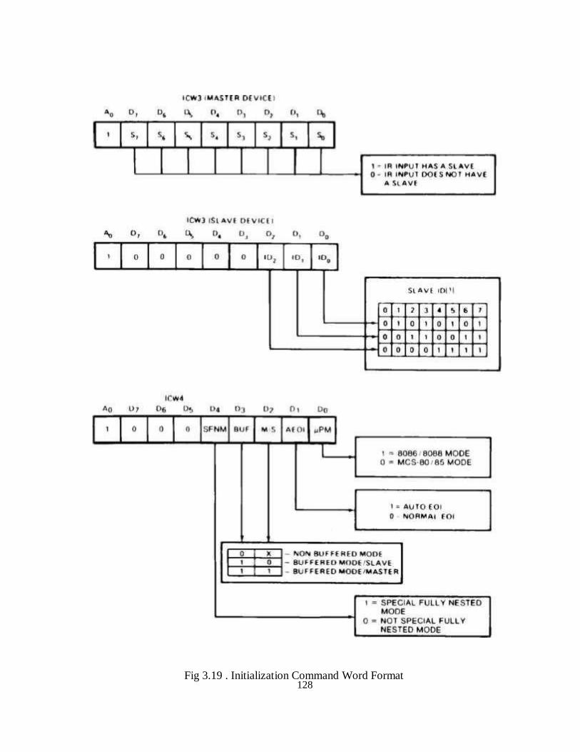
128
Fig 3.19 . Initialization Command Word Format

129
OPERATION COMMAND WORDS
After the Initialization Command Words (ICWs) are programmed into the 8259A, the chip
is ready to accept interrupt requests at its input lines. However, during the 8259A operation,
a selection of algorithms can command the 8259A to operate in various modes through the
Operation Command Words (OCWs). Operation Command Word format is as shown in
figure
Fig 3.20 a. Operational Control Words

130
Fig 3.20 b. Operation Command Word Format
INTERFACING MEMORY CHIPS WITH 8085
8085 has 16 address lines (A0 - A15), hence a maximum of 64 KB (= 216 bytes) of
memory locations can be interfaced with it. The memory address space of the 8085
takes values from0000H to FFFFH.
The 8085 initiates set of signals such as IO/M , RD and WR when it wants to read
from and write into memory. Similarly, each memory chip has signals such as CE or
CS (chip enable or chip select), OE or RD (output enable or read) and WE or WR
(write enable or write) associated with it.
Generation of Control Signals for Memory:
When the 8085 wants to read from and write into memory, it activates IO/M , RD
and WR signals as shown in Table .
131
Table 8 Status of IO/M , RD and WR signals during memory read and write operations
RD
WR
Operation IO/M
0 0 1 8085 reads data from memory
0 1 0 8085 writes data into memory
Using IO/M , RD and WR signals, two control signals MEMR (memory read) and
MEMW (memory write) are generated. Fig. 16 shows the circuit used to generate
thesesignals.
Fig. 3.21 Circuit used to generate MEMR and MEMW signals
When is IO/M high, both memory control signals are deactivated irrespective of the
statusof RD and WR signals.
Ex: Interface an IC 2764 with 8085 using NAND gate address decoder such
that theaddress range allocated to the chip is 0000H – 1FFFH.
Specification of IC 2764:
8 KB (8 x 210 byte) EPROM chip
13 address lines (213 bytes =
8 KB) Interfacing:

132
13 address lines of IC are connected to the corresponding address lines of
8085. Remaining address lines of 8085 are connected to address decoder
formed using logic gates, the output of which is connected to the CE pin of
IC. Address range allocated to the chip is shown in Table 9.
Chip is enabled whenever the 8085 places an address allocated to EPROM chip
in the address bus. This is shown in Fig. 17.
Fig. 3.22 Interfacing IC 2764 with the 8085 Table 9 Address allocated to IC 2764
Ex: Interface a 6264 IC (8K x 8 RAM) with the 8085 using NAND gate decoder
suchthat the starting address assigned to the chip is 4000H.
Specification of IC 6264:
8K x 8 RAM
133
8 KB = 213 bytes
13 address lines
The ending address of the chip is 5FFFH (since 4000H + 1FFFH = 5FFFH). When the
address 4000H to 5FFFH are written in binary form, the values in the lines A15, A14,
A13 are 0, 1 and 0 respectively. The NAND gate is designed such that when the lines
A15 and A13 carry 0 and A14 carries 1, the output of the NAND gate is 0. The
NAND gate output is in turn connected to the CE1 pin of the RAM chip. A NAND
output of 0 selects the RAM chip for read or write operation, since CE2 is already 1
because of its connection to +5V. Fig. 18 shows the interfacing of IC 6264 with the
8085.
Fig. 3.23 Interfacing 6264 IC with the 8085
Ex: Interface two 6116 ICs with the 8085 using 74LS138 decoder such that the
starting addresses assigned to them are 8000H and 9000H, respectively.
Specification of IC 6116:
2 K x 8 RAM
2 KB = 211 bytes
11 address lines
134
6116 has 11 address lines and since 2 KB, therefore ending addresses of 6116 chip 1
is and chip 2 are 87FFH and 97FFH, respectively. Table 10 shows the address range of
the two chips.
Table 3.1 Address range for IC 6116
Interfacing:
• Fig. 19 shows the interfacing.
• A0 – A10 lines of 8085 are connected to 11 address lines of the RAMchips.
• Three address lines of 8085 having specific value for a particular RAM are
connected to the three select inputs (C, B and A) of 74LS138 decoder.
• Table 10 shows that A13=A12=A11=0 for the address assigned to RAM 1 and
A13=0, A12=1 and A11=0 for the address assigned to RAM 2.
• Remaining lines of 8085 which are constant for the address range assigned to
the two RAM are connected to the enable inputs of decoder.
• When 8085 places any address between 8000H and 87FFH in the address bus,
the select inputs C, B and A of the decoder are all 0. The Y0 output of the
decoder is also 0, selecting RAM 1.

135
• When 8085 places any address between 9000H and 97FFH in the address bus,
the select inputs C, B and A of the decoder are 0, 1 and 0. The Y2 output of
the decoder is also 0, selecting RAM 2.
Fig. 3.24 Interfacing two 6116 RAM chips using 74LS138 decoder
3. PERIPHERAL MAPPED I/O INTERFACING
In this method, the I/O devices are treated differently from memory chips. The
control signals I/O read ( IOR ) and I/O write ( IOW ), which are derived from the
IO/M , RD and
WR signals of the 8085, are used to activate input and output
devices, respectively.
Generation of these control signals is shown in Fig. 20. Table 11 shows the status
of IO/M ,RD and WR signals during I/O read and I/O write operation.
136
Fig. 3.25 Generation of IOR and IOW signals
IN instruction is used to access input device and OUT instruction is used to access
output device. Each I/O device is identified by a unique 8-bit address assigned to it.
Since the control signals used to access input and output devices are different, and all
I/O device use 8-bit address, a maximum of 256 (28) input devices and 256 output
devices can be interfaced with 8085.
Table 3.2 Status of IOR and IOW signals in 8085.
IO/
M
RD
WR
IOR
IOW
Operation
1 0 1 0 1 I/O read operation
1 1 0 1 0 I/O write operation
0 X X 1 1 Memory read or write operation
Ex: Interface an 8-bit DIP switch with the 8085 such that the address assigned to
the DIPswitch if F0H.
IN instruction is used to get data from DIP switch and store it in accumulator.
Stepsinvolved in the execution of this instruction are:
• Address F0H is placed in the lines A0 – A7 and a copy of it in lines A8 –A15.
ii.
The IOR signal is activated ( IOR = 0), which makes the selected input
device to place its data in the data bus.
iii. The data in the data bus is read and store in the accumulator.

137
Fig. 3.26 shows the interfacing of DIP switch.
A7 A6 A5 A4 A3 A2 A1 A0
1 1 1 1 0 0 0 0 = F0H
A0 – A7 lines are connected to a NAND gate decoder such that the output of NAND gate is
0. The output of NAND gate is ORed with the IOR signal and the output of OR gateis
connected to 1G and 2G of the 74LS244. When 74LS244 is enabled, data from the
DIP switch is placed on the data bus of the 8085. The 8085 read data and store in the
accumulator. Thus data from DIP switch is transferred to the accumulator.
Fig. 3.26 interfacing of 8-bit DIP switch with 8085
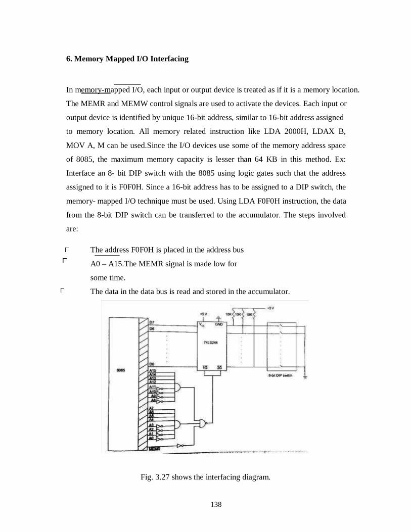
138
6. Memory Mapped I/O Interfacing
In memory-mapped I/O, each input or output device is treated as if it is a memory location.
The MEMR and MEMW control signals are used to activate the devices. Each input or
output device is identified by unique 16-bit address, similar to 16-bit address assigned
to memory location. All memory related instruction like LDA 2000H, LDAX B,
MOV A, M can be used.Since the I/O devices use some of the memory address space
of 8085, the maximum memory capacity is lesser than 64 KB in this method. Ex:
Interface an 8- bit DIP switch with the 8085 using logic gates such that the address
assigned to it is F0F0H. Since a 16-bit address has to be assigned to a DIP switch, the
memory- mapped I/O technique must be used. Using LDA F0F0H instruction, the data
from the 8-bit DIP switch can be transferred to the accumulator. The steps involved
are:
The address F0F0H is placed in the address bus
A0 – A15.The MEMR signal is made low for
some time.
The data in the data bus is read and stored in the accumulator.
Fig. 3.27 shows the interfacing diagram.
139
When 8085 executes the instruction LDA F0F0H, it places the address
F0F0Hin the address lines A0 – A15 as:
A15 A14 A13 A12 A11 A10 A9 A8 A7 A6 A5 A4 A3 A2 A1 A0
1 1 1 1 0 0 0 0 1 1 1 1 0 0 0 0= F0F0H
The address lines are connected to AND gates. The output of these gates along with
MEMR signal are connected to a NAND gate, so that when the address F0F0H is
placed in the address bus and MEMR = 0 its output becomes 0, thereby enabling the
buffer 74LS244. The data from the DIP switch is placed in the 8085 data bus. The
8085 reads the data from the data bus and stores it in the accumulator.
nterfacing ADC with 8085 Microprocessor
To interface the ADC with 8085, we need 8255 Programmable Peripheral Interface
chip with it. Let us see the circuit diagram of connecting 8085, 8255 and the ADC
converter.
Fig 3.28: ADC interfacing
140
The PortA of 8255 chip is used as the input port. The PC7 pin of Port Cupper is
connected to the End of Conversion (EOC) Pin of the analog to digital converter.
This port is also used as input port. The Clower port is used as output port. The PC2-
0 lines are connected to three address pins of this chip to select input channels. The
PC3 pin is connected to the Start of Conversion (SOC) pin and ALE pin of ADC
0808/0809.
Now let us see a program to generate digital signal from analog data. We are using
IN0 as input pin, so the pin selection value will be 00H.
Program
MVI A, 98H ; Set Port A and Cupper as input, CLower as
output OUT 03H ; Write control word 8255-I to control Word
register XRA A ; Clear the accumulator
OUT 02H ; Send the content of Acc to Port Clower to select
IN0
MVI A, 08H ; Load the accumulator with
08H OUT 02H ; ALE and SOC will be 0
XRA A ; Clear the accumulator
OUT 02H ; ALE and SOC will be low.
READ: IN 02H ; Read from EOC (PC7)
RAL ; Rotate left to check C7 is 1.
JNC READ ; If C7 is not 1, go to
READ IN 00H ; Read digital output
of ADC STA 8000H ; Save result at
8000H
HLT ; Stop the program
141
Fig 3.29: Flow chart-
ADC Either of the method can write the program.
Fig 3.30: control word format
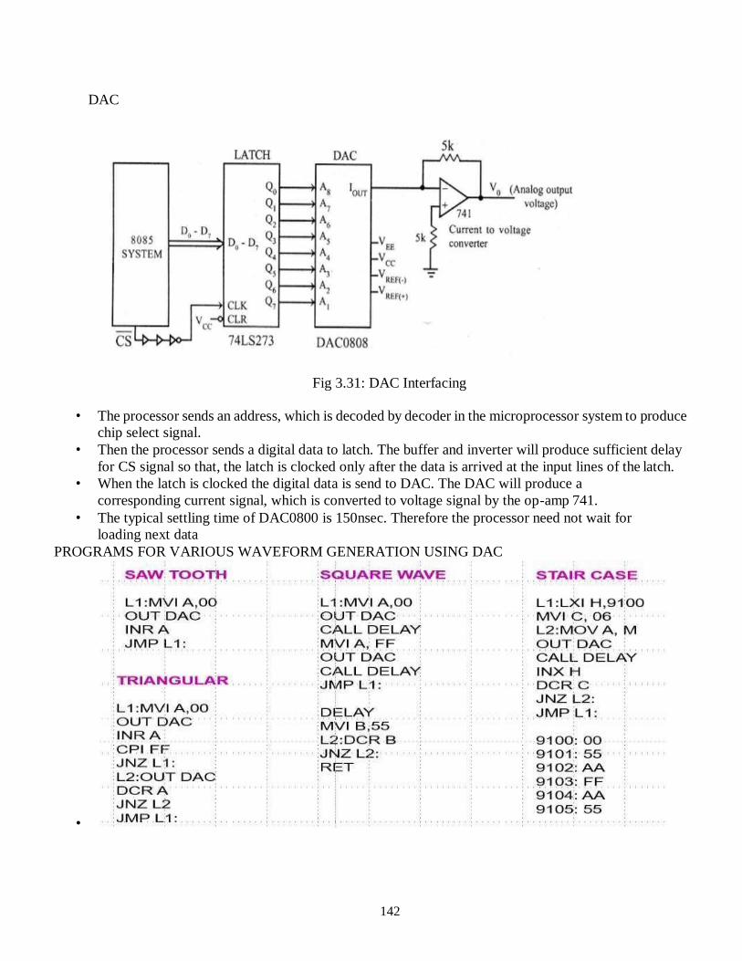
142
DAC
Fig 3.31: DAC Interfacing
• The processor sends an address, which is decoded by decoder in the microprocessor system to produce
chip select signal.
• Then the processor sends a digital data to latch. The buffer and inverter will produce sufficient delay
for CS signal so that, the latch is clocked only after the data is arrived at the input lines of the latch.
• When the latch is clocked the digital data is send to DAC. The DAC will produce a
corresponding current signal, which is converted to voltage signal by the op-amp 741.
• The typical settling time of DAC0800 is 150nsec. Therefore the processor need not wait for
loading next data
PROGRAMS FOR VARIOUS WAVEFORM GENERATION USING DAC
•

143
QUESTION BANK
PART A
1. What is interfacing
2. Distinguish memory mapped I/O and I/O mapped I/O
3. Draw the control word for 8255
4. Configure 8255 as PORT A-I/P, PORT B-O/P & PORT C LOWER-I/P , PORTC UPPER-O/P
5. Set PCO using bit set reset mode
6. Write the control word to generate square wave using 8253
7. What is the need of Priority resolver in 8259
8. How many interrupts maximum a 8259 can support
9. What is USART
10. Define resolution in DAC and ADC
11. What is EOC and SOC in ADC
12. Write an ALP to generate sawtooth using DAC
13. What are the two command words used in 8259 14. Explain mode 5 of 8253
15. Explain the transmitter section of 8251 USART
PART B
1. Explain with neat diagram 8255 PPI
2. With neat diagram explain how serial communication is done using 8251
3. With neat diagram explain the 8253 timer
4. Explain the various modes of 8253 timer
5. Discuss about 8259 PIC
6. Interface ADC to 8085 and explain
7. Interface DAC with 8085 and generate various waveforms
TEXT / REFERENCE BOOKS
3. Ramesh Gaonkar, ―Microprocessor Architecture, Programming and applications with 8085‖, 5th
Edition, Penram International Publishing Pvt Ltd, 2010.
2. Kenneth J Ayala, ―The 8051 Microcontroller‖, 2nd Edition, Thomson, 2005.
3. Nagoor Kani A, ―Microprocessor and Microcontroller‖, 2nd Edition, Tata McGraw Hill, 2012.
4. Mathur A.P. ‖ Introduction to microprocessor .―
5. Muhammad Ali Mazidi.‖The 8051 Microcontroller and Embedded Systems.‖
144
SCHOOL OF ELECTRICAL AND ELECTRONICS
DEPARTMENT OF ELECTRONICS AND COMMUNICATION ENGINEERING
UNIT – IV– MICROPROCESSORS AND MICROCONTROLLERS– SECA1601
145
UNIT 4 8051 MICROCONTROLLER
8051 Architecture: Microcontroller Hardware – I/O Pins, Ports – Internal and External memory
– Counters and Timers – Serial data I/O – Interrupts – 8051 Assembly Language Programming:
Addressing modes, Instruction set of 8051, Data transfer instructions, Arithmetic and Logical
Instructions, Jump and Call Instructions interrupts and return interrupts and return interrupt handling.
1.Architecture Of 8051 Microcontroller
An 8051 microcontroller has the following 11 major components:
1. ALU (Arithmetic and Logic Unit)
2. PC (Program Counter)
3. Registers
4. Timers and counters
5. Internal RAM and ROM
6. Four general purpose parallel input/output ports
7. Interrupt control logic with five sources of interrupt
8. Serial date communication
9. PSW (Program Status Word)
10. Data Pointer (DPTR)
11. Stack Pointer (SP)
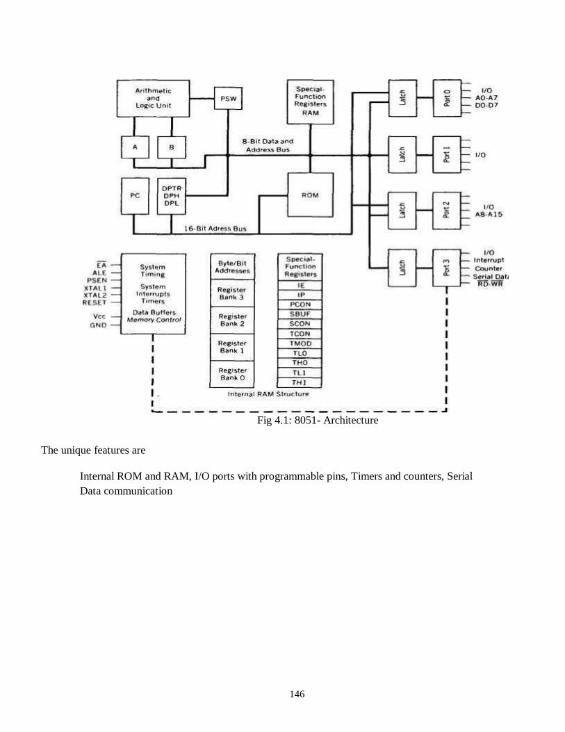
146
Fig 4.1: 8051- Architecture
The unique features are
Internal ROM and RAM, I/O ports with programmable pins, Timers and counters, Serial
Data communication

147
2.Programming Model Of 8051
Fig 4.2: Programming Model

148
The above diagram shows the programming model of
8051. The 8051 architecture consists of these specific
features:
8 bit CPU with registers A and B
16 bit PC and DPTR
8 bit Program status word (PSW)
8 bit Stack pointer(SP)
Internal ROM (4K)
Internal RAM of 128 bytes
4 register banks, each containing 8 registers
16 bytes, which may be addressed at the bitlevel
80 bytes of general purpose data memory
32 input/output pins arranged as four 8 bit ports: P0-P3
Two 16 bit Timers/Counters: T0 and T1
Full duplex serial data receiver/transmitter: SBUF
Control Register: TCON,TMOD,SCON,PCON,IP and IE
Two external and three internal interrupt sources
Oscillator and
clock circuits Special
Function Registers (SFRs)
Special Function Registers (SFRs) are a sort of control table used for running and monitoring the operation of the microcontroller. Each of these registers as well as each bit they
include, has its name, address in the scope of RAM and precisely defined purpose such as
timer control, interrupt control, serial communication control etc. Even though there are
128 memory locations intended to be occupied by them, the basic core, shared by all types of
8051 microcontrollers, has only 21 such registers. Rest of locations are intensionally left

149
unoccupied in order to enable the manufacturers to further develop microcontrollers
keeping them compatible with the previous versions. It also enables programs written a long
time ago for microcontrollers which are out of production now to be used today.
Fig 4.3 : SFR
A Register (Accumulator)
Fig 4.4: Accumulator
A register is a general-purpose register used for storing intermediate results obtained during
operation. Prior to executing an instruction upon any number or operand it is necessary to
store itin the accumulator first. All results obtained from arithmetical operations performed
by the ALU are stored in the accumulator. Data to be moved from one register to another
must go through theaccumulator. In other words, the A register is the most commonly used
register and it is impossible to imagine a microcontroller without it. More than half
instructions used by the 8051 microcontroller use somehow the accumulator.
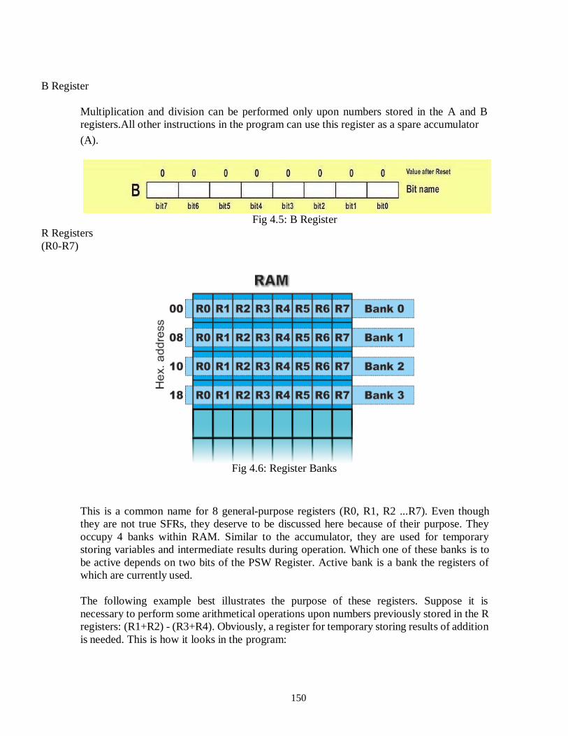
150
B Register
Multiplication and division can be performed only upon numbers stored in the A and B
registers.All other instructions in the program can use this register as a spare accumulator
(A).
R Registers
(R0-R7)
Fig 4.5: B Register
Fig 4.6: Register Banks
This is a common name for 8 general-purpose registers (R0, R1, R2 ...R7). Even though
they are not true SFRs, they deserve to be discussed here because of their purpose. They
occupy 4 banks within RAM. Similar to the accumulator, they are used for temporary
storing variables and intermediate results during operation. Which one of these banks is to
be active depends on two bits of the PSW Register. Active bank is a bank the registers of
which are currently used.
The following example best illustrates the purpose of these registers. Suppose it is
necessary to perform some arithmetical operations upon numbers previously stored in the R
registers: (R1+R2) - (R3+R4). Obviously, a register for temporary storing results of addition
is needed. This is how it looks in the program:
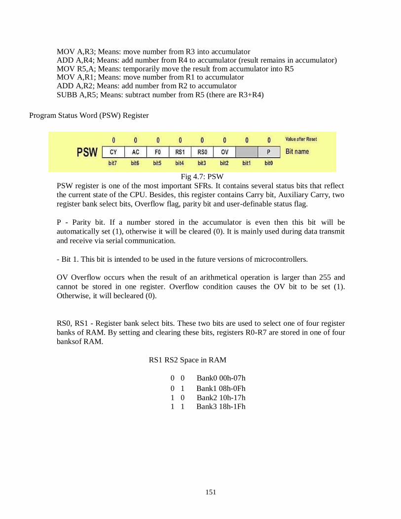
151
MOV A,R3; Means: move number from R3 into accumulator ADD A,R4; Means: add number from R4 to accumulator (result remains in accumulator) MOV R5,A; Means: temporarily move the result from accumulator into R5 MOV A,R1; Means: move number from R1 to accumulator ADD A,R2; Means: add number from R2 to accumulator
SUBB A,R5; Means: subtract number from R5 (there are R3+R4)
Program Status Word (PSW) Register
Fig 4.7: PSW
PSW register is one of the most important SFRs. It contains several status bits that reflect
the current state of the CPU. Besides, this register contains Carry bit, Auxiliary Carry, two
register bank select bits, Overflow flag, parity bit and user-definable status flag.
P - Parity bit. If a number stored in the accumulator is even then this bit will be
automatically set (1), otherwise it will be cleared (0). It is mainly used during data transmit
and receive via serial communication.
- Bit 1. This bit is intended to be used in the future versions of microcontrollers.
OV Overflow occurs when the result of an arithmetical operation is larger than 255 and
cannot be stored in one register. Overflow condition causes the OV bit to be set (1).
Otherwise, it will becleared (0).
RS0, RS1 - Register bank select bits. These two bits are used to select one of four register
banks of RAM. By setting and clearing these bits, registers R0-R7 are stored in one of four
banksof RAM.
RS1 RS2 Space in RAM
0 0 Bank0 00h-07h
0 1 Bank1 08h-0Fh
1 0 Bank2 10h-17h 1 1 Bank3 18h-1Fh
152
F0 - Flag 0. This is a general-purpose bit available for use.
AC - Auxiliary Carry Flag is used for BCD operations only.
CY - Carry Flag is the (ninth) auxiliary bit used for all arithmetical operations and shift
instructions.
Data Pointer Register (DPTR)
DPTR register is not a true one because it doesn't physically exist. It consists of two
separate registers: DPH (Data Pointer High) and (Data Pointer Low). For this reason it may
be treated as a16-bit register or as two independent 8-bit registers. Their 16 bits are
primarly used for external memory addressing. Besides, the DPTR Register is usually used
for storing data and intermediateresults.
Stack Pointer (SP)
Register
Fig 4.8: DPTR

153
Pin 9: RS
Fig 4.9: Stack Pointer
A value stored in the Stack Pointer points to the first free stack address and permits stack
availability. Stack pushes increment the value in the Stack Pointer by 1. Likewise, stack
pops decrement its value by 1. Upon any reset and power-on, the value 7 is stored in the
Stack Pointer,which means that the space of RAM reserved for the stack starts at this
location. If another value is written to this register, the entire Stack is moved to the new
memory location.
P0, P1, P2, P3 - Input/Output Registers
Fig 4.10: P0 If neither external memory nor serial communication system are used then 4 ports with in
total of32 input/output pins are available for connection to peripheral environment. Each bit
within theseports affects the state and performance of appropriate pin of the microcontroller.
Thus, bit logic state is reflected on appropriate pin as a voltage (0 or 5 V) and vice versa,
voltage on a pin reflects the state of appropriate port bit.
As mentioned, port bit state affects performance of port pins, i.e. whether they will be
configuredas inputs or outputs. If a bit is cleared (0), the appropriate pin will be configured
as an output, while if it is set (1), the appropriate pin will be configured as an input. Upon
reset and power-on, all port bits are set (1), which means that all appropriate pins will be
configured as inputs.
Pinout Description
Each of these pins can be configured as an input or an output.
A logic one on this pin disables the microcontroller and clears the contents of
most registers. In other words, the positive voltage on this pin resets the microcontroller.
By applying logic zero to this pin, the program starts execution from the beginning.
Similar to port 1, each of these pins can serve as general input or output.
Besides, all of them have alternative functions:
Pins10-17: Port 3
Pins 1-8: Port 1
154
Pin 18, 19: X2, X1
Pin 30: ALE
Pin 29: PSEN
Pin 21-28: Port 2
Serial asynchronous communication input or Serial synchronous communication
output.
Serial asynchronous communication output or Serial synchronous communication
clock output.
Interrupt 0 input.
Interrupt 1 input.
Counter 0 clock
input.Counter 1
Pin 16: WRclock input.
Write to external (additional)
RAM.Read from external
RAM.
Internal oscillator input and output. A quartz crystal which specifies
Operating frequency is usually connected to these pins. Instead of it, miniature ceramics resonators can also be used for frequency stability. Later versions of microcontrollers operate ata frequency of 0 Hz up to over 50 Hz.
Ground.
If there is no intention to use external memory then these port pins
areconfigured as general inputs/outputs. In case external memory is used, the higher
address byte, i.e. addresses A8-A15 will appear on this port. Even though memory with capacity of 64Kb is not used, which means that not all eight port bits are used for its addressing, the rest of
them arenot available as inputs/outputs.
If external ROM is used for storing program then a logic zero (0) appears
on itevery time the microcontroller reads a byte from memory.
Prior to reading from external memory, the microcontroller puts the lower
address byte (A0-A7) on P0 and activates the ALE output. After receiving signal from the
Pin 17: RD
Pin 15: T1
Pin 14: T0
Pin 13: INT1
Pin 12: INT0
Pin 11: TXD
Pin 10: RXD
Pin 20: GND
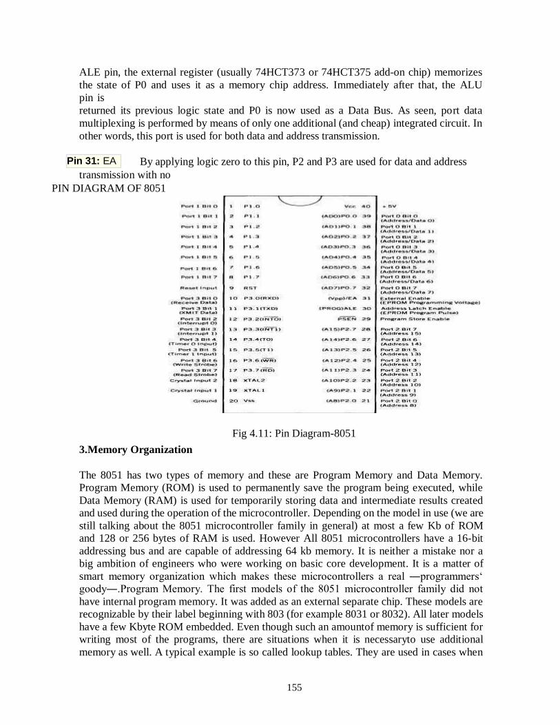
155
Pin 31: EA
ALE pin, the external register (usually 74HCT373 or 74HCT375 add-on chip) memorizes
the state of P0 and uses it as a memory chip address. Immediately after that, the ALU
pin is
returned its previous logic state and P0 is now used as a Data Bus. As seen, port data
multiplexing is performed by means of only one additional (and cheap) integrated circuit. In
other words, this port is used for both data and address transmission.
By applying logic zero to this pin, P2 and P3 are used for data and address
transmission with no
PIN DIAGRAM OF 8051
Fig 4.11: Pin Diagram-8051
3.Memory Organization
The 8051 has two types of memory and these are Program Memory and Data Memory.
Program Memory (ROM) is used to permanently save the program being executed, while
Data Memory (RAM) is used for temporarily storing data and intermediate results created
and used during the operation of the microcontroller. Depending on the model in use (we are
still talking about the 8051 microcontroller family in general) at most a few Kb of ROM
and 128 or 256 bytes of RAM is used. However All 8051 microcontrollers have a 16-bit
addressing bus and are capable of addressing 64 kb memory. It is neither a mistake nor a
big ambition of engineers who were working on basic core development. It is a matter of
smart memory organization which makes these microcontrollers a real ―programmers‘
goody―.Program Memory. The first models of the 8051 microcontroller family did not
have internal program memory. It was added as an external separate chip. These models are
recognizable by their label beginning with 803 (for example 8031 or 8032). All later models
have a few Kbyte ROM embedded. Even though such an amountof memory is sufficient for
writing most of the programs, there are situations when it is necessaryto use additional
memory as well. A typical example is so called lookup tables. They are used in cases when
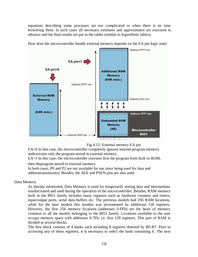
156
equations describing some processes are too complicated or when there is no time
forsolving them. In such cases all necessary estimates and approximates are executed in
advance and the final results are put in the tables (similar to logarithmic tables).
How does the microcontroller handle external memory depends on the EA pin logic state:
Fig 4.12: External memory EA pin
EA=0 In this case, the microcontroller completely ignores internal program memory
andexecutes only the program stored in external memory.
EA=1 In this case, the microcontroller executes first the program from built-in ROM,
then theprogram stored in external memory.
In both cases, P0 and P2 are not available for use since being used for data and
addresstransmission. Besides, the ALE and PSEN pins are also used.
Data Memory
As already mentioned, Data Memory is used for temporarily storing data and intermediate
resultscreated and used during the operation of the microcontroller. Besides, RAM memory
built in the 8051 family includes many registers such as hardware counters and timers,
input/output ports, serial data buffers etc. The previous models had 256 RAM locations,
while for the later models this number was incremented by additional 128 registers.
However, the first 256 memory locations (addresses 0-FFh) are the heart of memory
common to all the models belonging to the 8051 family. Locations available to the user
occupy memory space with addresses 0-7Fh, i.e. first 128 registers. This part of RAM is
divided in several blocks.
The first block consists of 4 banks each including 8 registers denoted by R0-R7. Prior to
accessing any of these registers, it is necessary to select the bank containing it. The next
157
memory block (address 20h-2Fh) is bit- addressable, which means that each bit has its own
address (0- 7Fh). Since there are 16 such registers, this block contains in total of 128 bits
with separate addresses (address of bit 0 of the 20h byte is 0, while address of bit 7 of the
2Fh byte is 7Fh). The third group of registers occupy addresses 2Fh-7Fh, i.e. 80 locations,
and does not have any special functions or features. Additional RAM In order to satisfy the programmers‘ constant hunger for Data Memory, the manufacturers
decided to embed an additional memory block of 128 locations into the latest versions of
the 8051 microcontrollers. However, it‘s not as simple as it seems to be… The problem is
that electronics performing addressing has 1 byte (8 bits) on disposal and is capable of
reaching only the first 256 locations, therefore. In order to keep already existing 8-bit
architecture and compatibility with other existing models a small trick was done.
What does it mean? It means that additional memory block shares the same addresses with
locations intended for the SFRs (80h- FFh). In order to differentiate between these two
physically separated memory spaces, different ways of addressing are used. The SFRs
memory locations are accessed by direct addressing, while additional RAM memory
locations are accessed by indirect addressing.

158
Fig 4.13 : Internal RAM
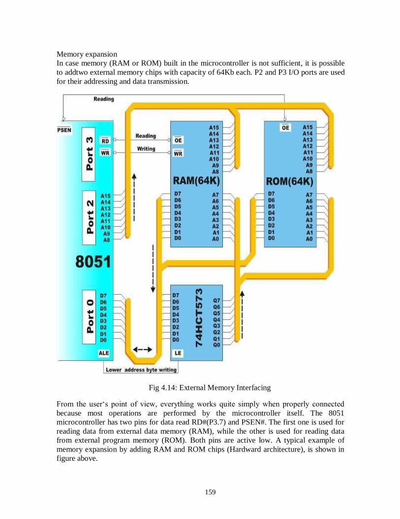
159
Memory expansion
In case memory (RAM or ROM) built in the microcontroller is not sufficient, it is possible
to addtwo external memory chips with capacity of 64Kb each. P2 and P3 I/O ports are used
for their addressing and data transmission.
Fig 4.14: External Memory Interfacing
From the user‘s point of view, everything works quite simply when properly connected
because most operations are performed by the microcontroller itself. The 8051
microcontroller has two pins for data read RD#(P3.7) and PSEN#. The first one is used for
reading data from external data memory (RAM), while the other is used for reading data
from external program memory (ROM). Both pins are active low. A typical example of
memory expansion by adding RAM and ROM chips (Hardward architecture), is shown in
figure above.

160
Even though additional memory is rarely used with the latest versions of the
microcontrollers, we will describe in short what happens when memory chips are connected according to the previous schematic. The whole process described below is performed
automatically.
When the program during execution encounters an instruction which resides in
external memory (ROM), the microcontroller will activate its control output ALE
and set the first 8 bits of address (A0-A7) on P0. IC circuit 74HCT573 passes the
first 8 bits to memory address pins.
A signal on the ALE pin latches the IC circuit 74HCT573 and immediately
afterwards 8 higher bits of address (A8-A15) appear on the port. In this way, a
desired location of additional program memory is addressed. It is left over to read its content.
Port P0 pins are configured as inputs, the PSEN pin is activated and the
microcontroller reads from memory chip.
Similar occurs when it is necessary to read location from external RAM. Addressing is
performed in the same way, while read and write are performed via signals appearing on the
control outputs RD (is short for read) or WR (is short for write).
4.Addressing Modes
An "addressing mode" refers to how you are addressing a given memory location. In
summary, the addressing modes are as follows, with an example of each:
Immediate Addressing MOV A,#20h
Direct Addressing MOV A,30h
Indirect Addressing MOV A,@R0
External Direct
A,@DPTR
MOVX
Code Indirect MOVC A,@A+DPTR
Each of these addressing modes provides important flexibility.
Immediate Addressing
Immediate addressing is so-named because the value to be stored in memory immediately
follows the operation code in memory. That is to say, the instruction itself dictates what
value will be stored in memory.
For example, the instruction:
MOV A,#6Ah
This instruction uses Immediate Addressing because the Accumulator will be loaded with the value that immediately follows; in this case 6A (hexidecimal).
Immediate addressing is very fast since the value to be loaded is included in the
instruction. However, since the value to be loaded is fixed at compile-time it is not very flexible.
161
Direct Addressing
Direct addressing is so-named because the value to be stored in memory is obtained by
directly retrieving it from another memory location. For example:
MOV A,30h
This instruction will read the data out of Internal RAM address 30 (hexidecimal) and store
it in the Accumulator.
Direct addressing is generally fast since, although the value to be loaded isnt included in
the instruction, it is quickly accessable since it is stored in the 8051s Internal RAM. It is
also much more flexible than Immediate Addressing since the value to be loaded is
whatever is found at thegiven address--which may be variable.
Also, it is important to note that when using direct addressing any instruction which refers
to an address between 00h and 7Fh is referring to Internal Memory. Any instruction which
refers to an address between 80h and FFh is referring to the SFR control registers that
control the 8051 microcontroller itself.
Indirect Addressing
Indirect addressing is a very powerful addressing mode which in many cases provides an
exceptional level of flexibility. Indirect addressing is also the only way to access the extra
128 bytes of Internal RAM found on an 8052.
Indirect addressing appears as follows:
MOV A,@R0
This instruction causes the 8051 to analyze the value of the R0 register. The 8051 will then
load the accumulator with the value from Internal RAM which is found at the address
indicated by R0.
For example, lets say R0 holds the value 40h and Internal RAM address 40h holds the
value 67h.When the above instruction is executed the 8051 will check the value of R0.
Since R0 holds 40h the 8051 will get the value out of Internal RAM address 40h (which
holds 67h) and store it in theAccumulator. Thus, the Accumulator ends up holding 67h.
Indirect addressing always refers to Internal RAM; it never refers to an SFR. Thus, in a
prior example we mentioned that SFR 99h can be used to write a value to the serial port.
Thus one may think that the following would be a valid solution to write the value 1 to the
serial port:
MOV R0,#99h ;Load the address of the serial port
MOV @R0,#01h ;Send 01 to the serial port -- WRONG!!
This is not valid. Since indirect addressing always refers to Internal RAM these two
instructions would write the value 01h to Internal RAM address 99h on an 8052. On an
8051 these two instructions would produce an undefined result since the 8051 only has 128
bytes
162
of Internal RAM.
External Direct
External Memory is accessed using a suite of instructions which use what I call "External
Direct"addressing. I call it this because it appears to be direct addressing, but it is used to
access externalmemory rather than internal memory.
There are only two commands that use External Direct addressing mode:
MOVXA,@DPT R
MOVX @DPTR,A
Both commands utilize DPTR. In these instructions, DPTR must first be loaded with the
address of external memory that you wish to read or write. Once DPTR holds the correct
external memory address, the first command will move the contents of that external memory
address into the Accumulator. The second command will do the opposite: it will allow you
to write the value of the Accumulator to the external memory address pointed to by DPTR.
External Indirect
External memory can also be accessed using a form of indirect addressing which I call
External Indirect addressing. This form of addressing is usually only used in relatively small
projects that have a very small amount of external RAM. An example of this addressing mode
is:
MOVX @R0,A
Once again, the value of R0 is first read and the value of the Accumulator is written to that
address in External RAM. Since the value of @R0 can only be 00h through FFh the project
would effectively be limited to 256 bytes of External RAM. There are relatively simple
hardware/software tricks that can be implemented to access more than 256 bytes of memory
using External Indirect addressing.
5.INSTRUCTION SET:
The process of writing program for the microcontroller mainly consists of giving instructions
(commands) in the specific order in which they should be executed in order to carry out a
specific task. As electronics cannot ―understand‖ what for example an instruction ―if the
push button is pressed- turn the light on‖ means, then a certain number of simpler and
precisely defined orders that decoder can recognise must be used. All commands are
known as INSTRUCTION SET. All microcontrollers compatibile with the 8051 have in
total of 255 instructions, i.e. 255 different words available for program writing.
At first sight, it is imposing number of odd signs that must be known by heart. However, It
is not so complicated as it looks like. Many instructions are considered to be ―different‖, even
though they perform the same operation, so there are only 111 truly different commands.
For example: ADD A,R0, ADD A,R1, ... ADD A,R7 are instructions that perform the
same

163
operation (additon of the accumulator and register). Since there are 8 such registers, each
instruction is counted separately. Taking into account that all instructions perform only 53
operations (addition, subtraction, copy etc.) and most of them are rarely used in practice,
there are actually 20-30 abbreviations to be learned, which is acceptable.
Types of instructions
Depending on operation they perform, all instructions are divided in several groups:
Arithmetic Instructions Branch Instructions Data Transfer Instructions Logic Instructions Bit-oriented Instructions
The first part of each instruction, called MNEMONIC refers to the operation aninstruction
performs (copy, addition, logic operation etc.). Mnemonics are abbreviations of the name
of operation being executed. For example:
INC R1 - Means: Increment register R1 (increment register R1);
LJMP LAB5 - Means: Long Jump LAB5 (long jump to the address marked as LAB5); JNZ LOOP - Means: Jump if Not Zero LOOP (if the number in the accumulator is
not 0, jump to the address marked as LOOP);
The other part of instruction, called OPERAND is separated from mnemonic by at least one
whitespace and defines data being processed by instructions. Some of the instructions have
no operand, while some of them have one, two or three. If there is more than one operand in
an instruction, they are separated by a comma. For example:
RET - return from a subroutine;
JZ TEMP - if the number in the accumulator is not 0, jump to the address marked as TEMP;
ADD A,R3 - add R3 and accumulator;
CJNE A,#20,LOOP - compare accumulator with 20. If they are not equal, jump
to the address marked as LOOP;
Arithmetic instructions
Arithmetic instructions perform several basic operations such as addition, subtraction,
division, multiplication etc. After execution, the result is stored in the first operand. For
example:
ADD A,R1 - The result of addition (A+R1) will be stored in the accumulator.
Arithmetic Instructions Mnemonic Description Byte Cycle
ADD A,Rn Adds the register to the accumulator 1 1
ADD A,direct Adds the direct byte to the accumulator 2 2
ADD A,@Ri Adds the indirect RAM to the accumulator 1 2
ADD A,#data Adds the immediate data to the accumulator 2 2

164
ADDC A,Rn Adds the register to the accumulator with a carry flag 1 1
ADDC
A,direct
Adds the direct byte to the accumulator with a carry flag 2 2
ADDC A,@Ri Adds the indirect RAM to the accumulator with a carry flag 1 2
ADDC Adds the immediate data to the accumulator with a carry flag 2 2
A,#data
SUBB A,Rn Subtracts the register from the accumulator with a borrow 1 1
SUBB A,direct Subtracts the direct byte from the accumulator with a borrow 2 2
SUBB A,@Ri Subtracts the indirect RAM from the accumulator with a borrow 1 2
SUBB A,#data Subtracts the immediate data from the accumulator with a borrow 2 2
INC A Increments the accumulator by 1 1 1
INC Rn Increments the register by 1 1 2
INC Rx Increments the direct byte by 1 2 3
INC @Ri Increments the indirect RAM by 1 1 3
DEC A Decrements the accumulator by 1 1 1
DEC Rn Decrements the register by 1 1 1
DEC Rx Decrements the direct byte by 1 1 2
DEC @Ri Decrements the indirect RAM by 1 2 3
INC DPTR Increments the Data Pointer by 1 1 3
MUL AB Multiplies A and B 1 5
DIV AB Divides A by B 1 5
DA A Decimal adjustment of the accumulator according to BCD code 1 1
Branch Instructions
There are two kinds of branch instructions:
Unconditional jump instructions: upon their execution a jump to a new location from
where theprogram continues execution is executed.
Conditional jump instructions: a jump to a new program location is executed only if
a specifiedcondition is met. Otherwise, the program normally proceeds with the next
instruction.

165
Fig 4.15: Jump Address Range
Branch Instructions
Mnemonic Description Byte Cycle
ACALL addr11 Absolute subroutine call 2 6
LCALL addr16 Long subroutine call 3 6
RET Returns from subroutine 1 4
RETI Returns from interrupt subroutine 1 4
AJMP addr11 Absolute jump 2 3
LJMP addr16 Long jump 3 4
SJMP rel Short jump (from –128 to +127 locations relative to the following 2 instruction)
3
JC rel Jump if carry flag is set. Short jump. 2 3
JNC rel Jump if carry flag is not set. Short jump. 2 3
JB bit,rel Jump if direct bit is set. Short jump. 3 4
JBC bit,rel Jump if direct bit is set and clears bit. Short jump. 3 4
JMP @A+DPTR JZ rel
Jump indirect relative to the DPTR Jump if the accumulator is zero. Short jump.
1 2
2 3
JNZ rel Jump if the accumulator is not zero. Short jump. 2 3
CJNE A,direct,rel Compares direct byte to the accumulator and jumps if not equal. 34 Short jump.
CJNE A,#data,rel Compares immediate data to the accumulator and jumps if not 34 equal. Short jump.
CJNE Rn,#data,rel

166
CJNE DJNZ Rn,rel Decrements register and jumps if not 0. Short jump. 2 3
DJNZ Rx,rel Decrements direct byte and jump if not 0. Short jump. 3 4 NOP No operation 1 1
Data Transfer Instructions
Data transfer instructions move the content of one register to another. The register the
content of which is moved remains unchanged. If they have the suffix ―X‖ (MOVX), the data
is exchanged with external memory.
Data Transfer Instructions
Mnemonic Description Byte Cycle
MOV A,Rn Moves the register to the accumulator 1 1
MOV A,direct Moves the direct byte to the accumulator 2 2
MOV A,@Ri Moves the indirect RAM to the accumulator 1 2
MOV A,#data Moves the immediate data to the accumulator 2 2
MOV Rn,A Moves the accumulator to the register 1 2
MOV Rn,direct Moves the direct byte to the register 2 4
MOV Rn,#data Moves the immediate data to the register 2 2
MOV direct,A Moves the accumulator to the direct byte 2 3
MOV direct,Rn Moves the register to the direct byte 2 3
MOV direct,direct Moves the direct byte to the direct byte 3 4
MOV direct,@Ri Moves the indirect RAM to the direct byte 2 4
MOV direct,#data Moves the immediate data to the direct byte 3 3
MOV @Ri,A Moves the accumulator to the indirect RAM 1 3
MOV @Ri,direct Moves the direct byte to the indirect RAM 2 5
MOV @Ri,#data Moves the immediate data to the indirect RAM 2 3
MOV DPTR,#data Moves a 16-bit data to the data pointer 3 3
MOVC Moves the code byte relative to the DPTR to the accumula tor 1 3
A,@A+DPTR (address=A+DPTR)
MOVC A,@A+PC Moves the code byte relative to the PC to the accumulator 1 3 (address=A+PC)
MOVX A,@Ri Moves the external RAM (8-bit address) to the accumulator 1 3-10
OVX A,@DPTR Moves the external RAM (16-bit address) to the accumulator 1 3-10
MOVX @Ri,A Moves the accumulator to the external RAM (8-bit address) 1 4-11
MOVX Moves the accumulator to the external RAM (16-bit address) 1 4-11
@DPTR,A
PUSH direct Pushes the direct byte onto the stack 2 4
POP direct Pops the direct byte from the stack/td> 2 3
XCH A,Rn Exchanges the register with the accumulator 1 2
XCH A,direct Exchanges the direct byte with the accumulator 2 3
XCH A,@Ri Exchanges the indirect RAM with the accumulator 1 3

167
XCHD A,@Ri Exchanges the low-order nibble indirect RAM with the 1 3 accumulator
Logic Instructions
Logic instructions perform logic operations upon corresponding
bits of execution, the result is stored in the first operand.
two registers. After
Logic Instructions
Mnemonic Description Byte Cycle
ANL A,Rn AND register to accumulator 1 1
ANL A,direct AND direct byte to accumulator 2 2
ANL A,@Ri AND indirect RAM to accumulator 1 2
ANL A,#data AND immediate data to accumulator 2 2
ANL direct,A AND accumulator to direct byte 2 3
ANL direct,#data AND immediae data to direct register 3 4
ORL A,Rn OR register to accumulator 1 1
ORL A,direct OR direct byte to accumulator 2 2
ORL A,@Ri OR indirect RAM to accumulator 1 2
ORL direct,A OR accumulator to direct byte 2 3
ORL direct,#data OR immediate data to direct byte 3 4
XRL A,Rn Exclusive OR register to accumulator 1 1
XRL A,direct Exclusive OR direct byte to accumulator 2 2
XRL A,@Ri Exclusive OR indirect RAM to accumulator 1 2
XRL A,#data Exclusive OR immediate data to accumulator 2 2
XRL direct,A Exclusive OR accumulator to direct byte 2 3
XORL direct,#data Exclusive OR immediate data to direct byte 3 4
CLR A Clears the accumulator 1 1
CPL A Complements the accumulator (1=0, 0=1) 1 1
SWAP A Swaps nibbles within the accumulator 1 1
RL A Rotates bits in the accumulator left 1 1
RLC A Rotates bits in the accumulator left through carry 1 1
RR A Rotates bits in the accumulator right 1 1
RRC A Rotates bits in the accumulator right through carry 1 1
168
Bit-oriented Instructions
Similar to logic instructions, bit-oriented instructions perform logic operations.
The difference isthat these are performed upon single bits.
Bit-oriented Instructions
Mnemonic Description Byte Cycle
CLR C Clears the carry flag 1 1
CLR bit Clears the direct bit 2 3
SETB C Sets the carry flag 1 1
SETB bit Sets the direct bit 2 3
CPL C Complements the carry flag 1 1
CPL bit Complements the direct bit 2 3
ANL C,bit AND direct bit to the carry flag 2 2
ANL C,/bit AND complements of direct bit to the carry flag
2 2 ORL C,bit OR direct bit to the carry flag
2 2 ORL C,/bit OR complements of direct bit to the carry
flag 2 2 MOV C,bit Moves the direct bit to the carry flag
2 2 MOV bit,C Moves the carry flag to the direct bit
2 3
6.8051 Microcontroller Interrupts
There are five interrupt sources for the 8051, which means that they can recognize 5
different events that can interrupt regular program execution. Each interrupt can be
enabled or disabled bysetting bits of the IE register. Likewise, the whole interrupt system
can be disabled by clearing the EA bit of the same register. Refer to figure below.
Now, it is necessary to explain a few details referring to external interrupts- INT0 and
INT1. Ifthe IT0 and IT1 bits of the TCON register are set, an interrupt will be generated
on high to lowtransition, i.e. on the falling pulse edge (only in that moment). If these bits
are cleared, an interrupt will be continuously executed as far as the pins are held low.
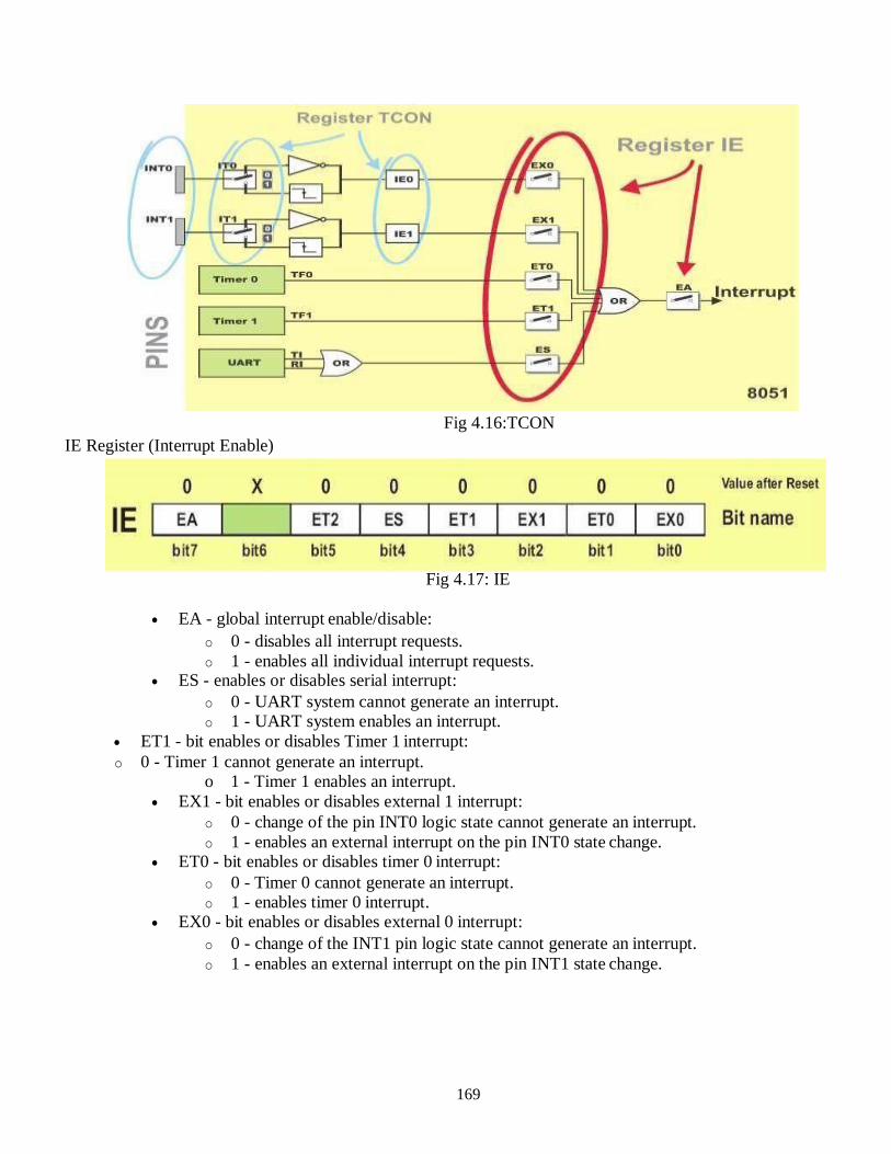
169
Fig 4.16:TCON
IE Register (Interrupt Enable)
Fig 4.17: IE
EA - global interrupt enable/disable:
o 0 - disables all interrupt requests.
o 1 - enables all individual interrupt requests. ES - enables or disables serial interrupt:
o 0 - UART system cannot generate an interrupt. o 1 - UART system enables an interrupt.
ET1 - bit enables or disables Timer 1 interrupt:
o 0 - Timer 1 cannot generate an interrupt. o 1 - Timer 1 enables an interrupt.
EX1 - bit enables or disables external 1 interrupt:
o 0 - change of the pin INT0 logic state cannot generate an interrupt.
o 1 - enables an external interrupt on the pin INT0 state change. ET0 - bit enables or disables timer 0 interrupt:
o 0 - Timer 0 cannot generate an interrupt. o 1 - enables timer 0 interrupt.
EX0 - bit enables or disables external 0 interrupt:
o 0 - change of the INT1 pin logic state cannot generate an interrupt.
o 1 - enables an external interrupt on the pin INT1 state change.

170
Interrupt Priorities
It is not possible to forseen when an interrupt request will arrive. If several
interrupts areenabled, it may happen that while one of them is in progress, another one is
requested. In order
that the microcontroller knows whether to continue operation or meet a new interrupt
request,there is a priority list instructing it what to do.
The priority list offers 3 levels of interrupt priority:
1. Reset! The apsolute master. When a reset request arrives, everything is stopped
and the microcontroller restarts.
2. Interrupt priority 1 can be disabled by Resetonly.
3. Interrupt priority 0 can be disabled by both Reset and interrupt priority1.
The IP Register (Interrupt Priority Register) specifies which one of existing interrupt
sourceshave higher and which one has lower priority. Interrupt priority is usually
specified at the beginning of the program. According to that, there are several
possibilities:
If an interrupt of higher priority arrives while an interrupt is in progress, it
willbe immediately stopped and the higher priority interrupt will be
executed first.
If two interrupt requests, at different priority levels, arrive at the same time
then the higher priority interrupt is serviced first.
If the both interrupt requests, at the same priority level, occur one after another,
the one which came later has to wait until routine being in progress ends.
If two interrupt requests of equal priority arrive at the same time then the interrupt to be serviced is selected according to the following priority list:
1. External interrupt INT0
2. Timer 0 interrupt
3. External Interrupt INT1
4. Timer 1 interrupt
5. Serial Communication Interrupt
IP Register (Interrupt Priority)
The IP register bits specify the priority level of each interrupt (high or low priority).
Fig 4.18: IP
171
PS - Serial Port Interrupt priority bit
o Priority 0
o Priority 1 PT1 - Timer 1 interrupt priority
o Priority 0
o Priority 1 PX1 - External Interrupt INT1 priority
o Priority 0
o Priority 1 PT0 - Timer 0 Interrupt Priority
o Priority 0
o Priority 1 PX0 - External Interrupt INT0 Priority
o Priority 0
o Priority 1
Handling Interrupt
When an interrupt request arrives the following occurs:
1. Instruction in progress is ended.
2. The address of the next instruction to execute is pushed on the stack.
3. Depending on which interrupt is requested, one of 5 vectors (addresses) is written tothe program counter in accordance to the table below:
4.
Interrupt Source Vector (address)
IE0 3 h
TF0 B h
TF1 1B h
RI, TI 23 h
All addresses are in hexadecimal format
5. These addresses store appropriate subroutines processing interrupts. Instead of
them, there are usually jump instructions specifying locations on which these
subroutines reside.
6. When an interrupt routine is executed, the address of the next instruction to
execute is poped from the stack to the program counter and interrupted program
resumes operation from where it left off.
Reset
Reset occurs when the RS pin is supplied with a positive pulse in duration of at least 2
machine cycles (24 clock cycles of crystal oscillator). After that, the microcontroller
generates an internal reset signal which clears all SFRs, except SBUF registers, Stack Pointer
and ports (the state of the first two ports is not defined, while FF value is written to the ports
configuring all their pins as inputs). Depending on surrounding and purpose of device, the
RS pin is usually connected to apower-on reset push button or circuit or to both of them.
Figure below illustrates one of the simplest circuit providing safe power-on reset.
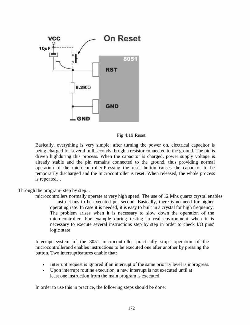
172
Fig 4.19:Reset
Basically, everything is very simple: after turning the power on, electrical capacitor is
being charged for several milliseconds throgh a resistor connected to the ground. The pin is
driven highduring this process. When the capacitor is charged, power supply voltage is
already stable and the pin remains connected to the ground, thus providing normal
operation of the microcontroller.Pressing the reset button causes the capacitor to be
temporarily discharged and the microcontroller is reset. When released, the whole process
is repeated…
Through the program- step by step...
microcontrollers normally operate at very high speed. The use of 12 Mhz quartz crystal enables instructions to be executed per second. Basically, there is no need for higher
operating rate. In case it is needed, it is easy to built in a crystal for high frequency.
The problem arises when it is necessary to slow down the operation of the
microcontroller. For example during testing in real environment when it is
necessary to execute several instructions step by step in order to check I/O pins'
logic state.
Interrupt system of the 8051 microcontroller practically stops operation of the
microcontrollerand enables instructions to be executed one after another by pressing the
button. Two interruptfeatures enable that:
Interrupt request is ignored if an interrupt of the same priority level is inprogress.
Upon interrupt routine execution, a new interrupt is not executed until at
least one instruction from the main program is executed.
In order to use this in practice, the following steps should be done:
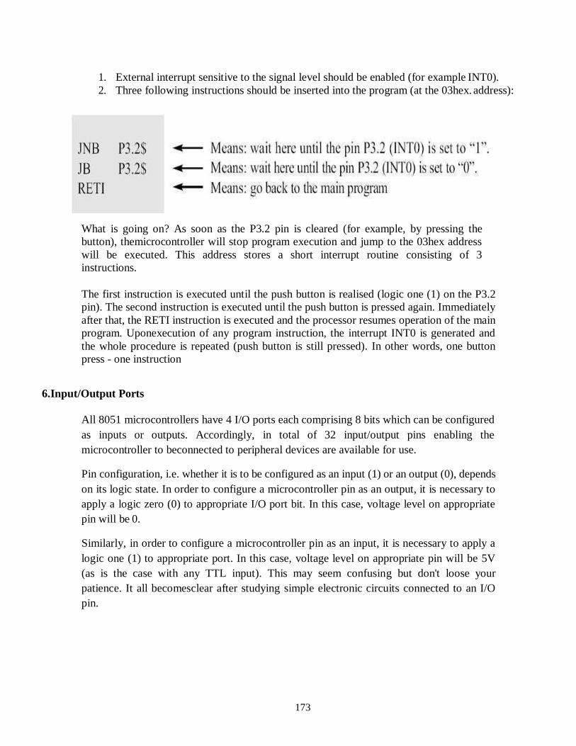
173
1. External interrupt sensitive to the signal level should be enabled (for example INT0).
2. Three following instructions should be inserted into the program (at the 03hex. address):
What is going on? As soon as the P3.2 pin is cleared (for example, by pressing the
button), themicrocontroller will stop program execution and jump to the 03hex address
will be executed. This address stores a short interrupt routine consisting of 3
instructions.
The first instruction is executed until the push button is realised (logic one (1) on the P3.2
pin). The second instruction is executed until the push button is pressed again. Immediately
after that, the RETI instruction is executed and the processor resumes operation of the main
program. Uponexecution of any program instruction, the interrupt INT0 is generated and
the whole procedure is repeated (push button is still pressed). In other words, one button
press - one instruction
6.Input/Output Ports
All 8051 microcontrollers have 4 I/O ports each comprising 8 bits which can be configured
as inputs or outputs. Accordingly, in total of 32 input/output pins enabling the
microcontroller to beconnected to peripheral devices are available for use.
Pin configuration, i.e. whether it is to be configured as an input (1) or an output (0), depends
on its logic state. In order to configure a microcontroller pin as an output, it is necessary to
apply a logic zero (0) to appropriate I/O port bit. In this case, voltage level on appropriate
pin will be 0.
Similarly, in order to configure a microcontroller pin as an input, it is necessary to apply a
logic one (1) to appropriate port. In this case, voltage level on appropriate pin will be 5V
(as is the case with any TTL input). This may seem confusing but don't loose your
patience. It all becomesclear after studying simple electronic circuits connected to an I/O
pin.
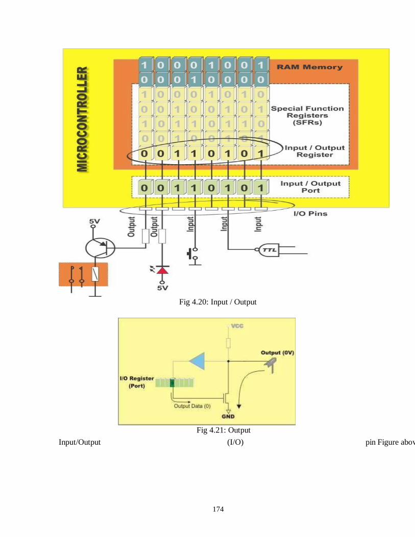
174
Fig 4.20: Input / Output
Fig 4.21: Output
Input/Output (I/O) pin Figure above illustrates a simplified schematic of all circuits within the microcontroller connected to one of its pins. It refers to all the pins except those of the P0 port which do not havepull-up resistors built-in.

175
Fig 4.22: Input / output
Output pin
A logic zero (0) is applied to a bit of the P register. The output FE transistor is turned on,
thus connecting the appropriate pin to ground.
Fig 4.23 output
Hardware interrupts of 8085
Input
pin
A logic one (1) is applied to a bit of the P register. The output FE transistor is turned off and
theappropriate pin remains connected to the power supply voltage over a pull-up resistor of
high resistance.
Logic state (voltage) of any pin can be changed or read at any moment. A logic zero (0) and
logic one (1) are not equal. A logic one (0) represents a short circuit to ground. Such a pin
acts asan output.
A logic one (1) is ―loosely‖ connected to the power supply voltage over a resistor of high
resistance. Since this voltage can be easily ―reduced‖ by an external signal, such a pin acts as.

176
The P0 port is characterized by two functions. If external memory is used then the lower
address byte (addresses A0-A7) is applied on it. Otherwise, all bits of this port are configured as
inputs/outputs.The other function is expressed when it is configured as an output. Unlike other
ports consisting of pins with built-in pull-up resistor connected by its end to 5 V power
supply, pins of this port have this resistor left out. This apparently small difference has its
consequences:
Fig 4.24: Port 0 configuration-input
If any pin of this port is configured as an input then it acts as if it ―floats‖. Such an input has
unlimited input resistance and indetermined potential.
Fig 4.25: Port 0 configuration-output
When the pin is configured as an output, it acts as an ―open drain‖. By applying logic 0 to a port
bit, the appropriate pin will be connected to ground (0V). By applying logic 1, the external
output will keep on ―floating‖. In order to apply logic 1 (5V) on this output pin, it is necessary to
built in an external pull-up resistor.Only in case P0 is used for addressing external memory,
the microcontroller will provide internalpower supply source in order to supply its pins with
logic one. There is no need to add
177
PORT A
P2 acts similarly to P0 when external memory is used. Pins of this port occupy addresses
intended for external memory chip. This time it is about the higher address byte with
addresses A8-A15. When no memory is added, this port can be used as a general input/output
port showingfeatures similar to P1.
Port 3
All port pins can be used as general I/O, but they also have an alternative function. In order
to use these alternative functions, a logic one (1) must be applied to appropriate bit of the P3
register. In tems of hardware, this port is similar to P0, with the difference that its pins have
a pull-up resistor built-in.
Pin's Current limitations
When configured as outputs (logic zero (0)), single port pins can receive a current of
10mA. If all8 bits of a port are active, a total current must be limited to 15mA (port P0:
26mA). If all ports (32 bits) are active, total maximum current must be limited to 71mA.
When these pins are configured as inputs (logic 1), built-in pull-up resistors provide very
weak current, but strong enough to activate up to 4 TTL inputs of LS series.
As seen from description of some ports, even though all of them have more or less similar
architecture, it is necessary to pay attention to which of them is to be used for what and how.
For example, if they shall be used as outputs with high voltage level (5V), then P0 should
be avoided because its pins do not have pull-up resistors, thus giving low logic level only.
When using other ports, one should have in mind that pull-up resistors have a relatively
high resistance,so that their pins can give a current of several hundreds microamperes only.
Counters and Timers
As you already know, the microcontroller oscillator uses quartz crystal for its operation. As
the frequency of this oscillator is precisely defined and very stable, pulses it generates are
always of the same width, which makes them ideal for time measurement. Such crystals are
also used in quartz watches. In order to measure time between two events it is sufficient to
count up pulses coming from this oscillator. That is exactly what the timer does. If thetimer
is properly programmed, the value stored in its register will be incremented (or
decremented) with each coming pulse, i.e. once per each machine cycle. A single machine-
cycle instruction lasts for 12 quartz oscillator periods, which means that by embedding
quartz with oscillator frequency of 12MHz, a number stored in the timer register will be
changed million times per second, i.e. each microsecond.
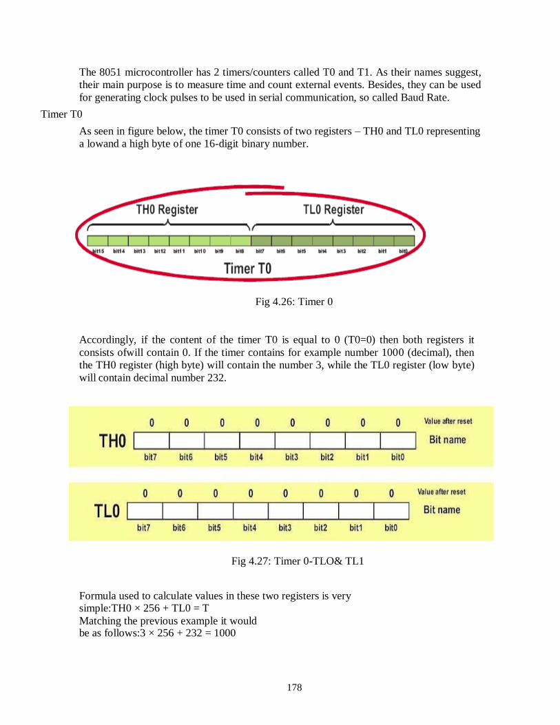
178
The 8051 microcontroller has 2 timers/counters called T0 and T1. As their names suggest,
their main purpose is to measure time and count external events. Besides, they can be used
for generating clock pulses to be used in serial communication, so called Baud Rate.
Timer T0
As seen in figure below, the timer T0 consists of two registers – TH0 and TL0 representing
a lowand a high byte of one 16-digit binary number.
Fig 4.26: Timer 0
Accordingly, if the content of the timer T0 is equal to 0 (T0=0) then both registers it
consists ofwill contain 0. If the timer contains for example number 1000 (decimal), then
the TH0 register (high byte) will contain the number 3, while the TL0 register (low byte)
will contain decimal number 232.
Fig 4.27: Timer 0-TLO& TL1
Formula used to calculate values in these two registers is very simple:TH0 × 256 + TL0 = T
Matching the previous example it would be as follows:3 × 256 + 232 = 1000

179
Fig 4.28: Timer 0
Since the timer T0 is virtually 16-bit register, the largest value it can store is 65 535. In
case ofexceeding this value, the timer will be automatically cleared and counting starts
from 0. This condition is called an overflow. Two registers TMOD and TCON are
closely connected to thistimer and control its operation.
TMOD Register (Timer Mode)
The TMOD register selects the operational mode of the timers T0 and T1. As seen in
figure below, the low 4 bits (bit0 - bit3) refer to the timer 0, while the high 4 bits (bit4 -
bit7) refer tothe timer 1. There are 4 operational modes and each of them is described
herein.
Fig 4.29: TMOD
Bits of this register have the following function:
GATE1 enables and disables Timer 1 by means of a signal brought to the
INT1 pin (P3.3):
o 1 - Timer 1 operates only if the INT1 bit is set.
o 0 - Timer 1 operates regardless of the logic state of the INT1 bit. C/T1 selects pulses to be counted up by the timer/counter 1:
o 1 - Timer counts pulses brought to the T1 pin (P3.5). o 0 - Timer counts pulses from internal oscillator.
T1M1,T1M0 These two bits select the operational mode of the Timer 1.
T1M1 T1M0 Mode Description
0 0 0 13-bit timer
0 1 1 16-bit timer
1 0 2 8-bit auto-reload

180
1 1 3 Split mode
GATE0 enables and disables Timer 1 using a signal brought to the INT0 pin (P3.2):
o 1 - Timer 0 operates only if the INT0 bit is set.
o 0 - Timer 0 operates regardless of the logic state of the INT0 bit. C/T0 selects pulses to be counted up by the timer/counter 0:
o 1 - Timer counts pulses brought to the T0 pin (P3.4).
o 0 - Timer counts pulses from internal oscillator. T0M1,T0M0 These two bits select the oprtaional mode of the Timer 0.
T0M1 T0M0 Mode
Descriptio
n
0 0 0 13-bit timer
0 1 1 16-bit timer
1 0 2 8-bit auto-reload
1 1 3 Split mode
Timer 0 in mode 0 (13-bit timer)
This is one of the rarities being kept only for the purpose of compatibility with the previuos
versions of microcontrollers. This mode configures timer 0 as a 13-bit timer which consists
of all8 bits of TH0 and the lower 5 bits of TL0. As a result, the Timer 0 uses only 13 of 16
bits. How does it operate? Each coming pulse causes the lower register bits to change their
states. After receiving 32 pulses, this register is loaded and automatically cleared, while the
higher byte (TH0)is incremented by 1. This process is repeated until registers count up
8192 pulses. After that, both registers are cleared and counting starts from 0.
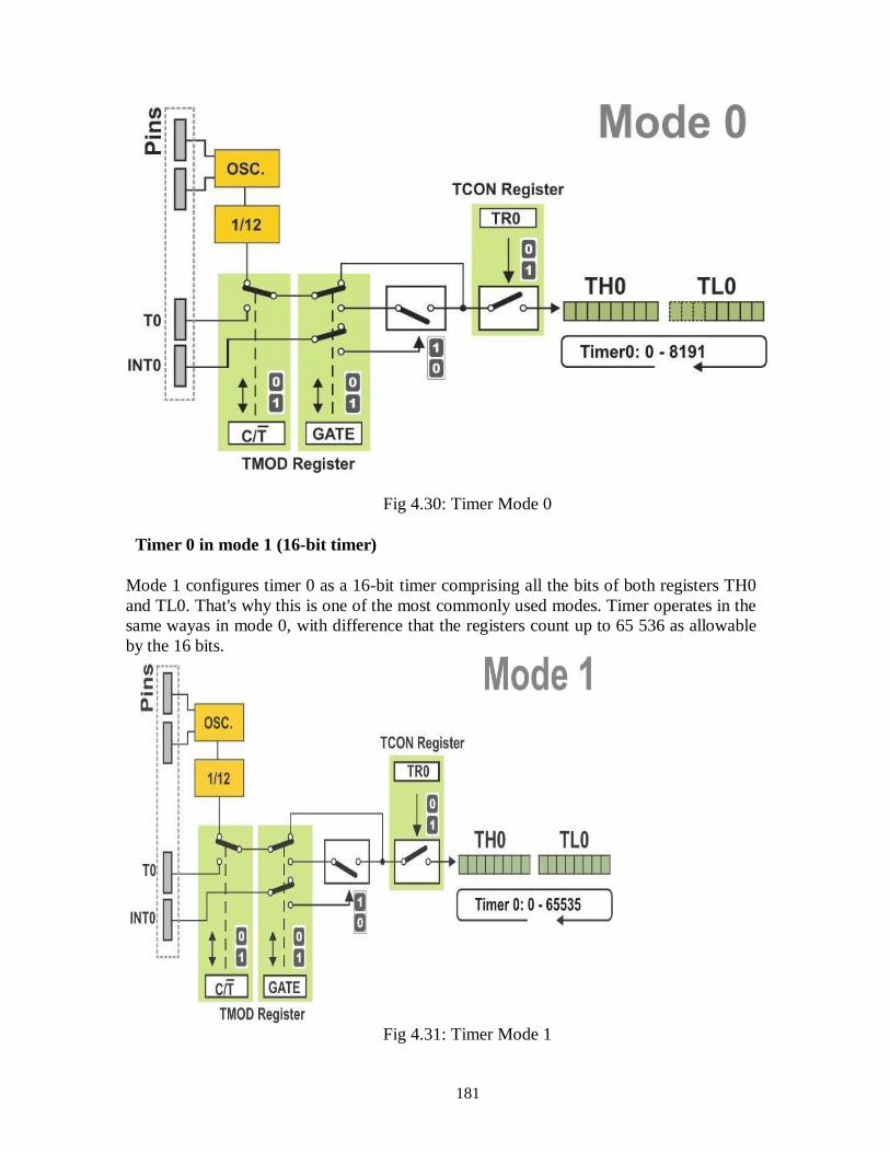
181
Fig 4.30: Timer Mode 0
Timer 0 in mode 1 (16-bit timer)
Mode 1 configures timer 0 as a 16-bit timer comprising all the bits of both registers TH0
and TL0. That's why this is one of the most commonly used modes. Timer operates in the
same wayas in mode 0, with difference that the registers count up to 65 536 as allowable
by the 16 bits.
Fig 4.31: Timer Mode 1
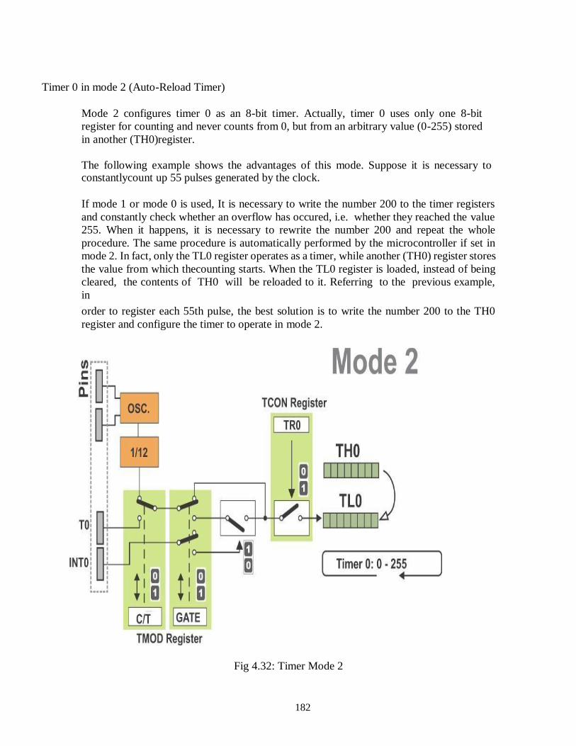
182
Timer 0 in mode 2 (Auto-Reload Timer)
Mode 2 configures timer 0 as an 8-bit timer. Actually, timer 0 uses only one 8-bit
register for counting and never counts from 0, but from an arbitrary value (0-255) stored
in another (TH0)register.
The following example shows the advantages of this mode. Suppose it is necessary to constantlycount up 55 pulses generated by the clock.
If mode 1 or mode 0 is used, It is necessary to write the number 200 to the timer registers
and constantly check whether an overflow has occured, i.e. whether they reached the value
255. When it happens, it is necessary to rewrite the number 200 and repeat the whole
procedure. The same procedure is automatically performed by the microcontroller if set in
mode 2. In fact, only the TL0 register operates as a timer, while another (TH0) register stores
the value from which thecounting starts. When the TL0 register is loaded, instead of being
cleared, the contents of TH0 will be reloaded to it. Referring to the previous example,
in
order to register each 55th pulse, the best solution is to write the number 200 to the TH0
register and configure the timer to operate in mode 2.
Fig 4.32: Timer Mode 2
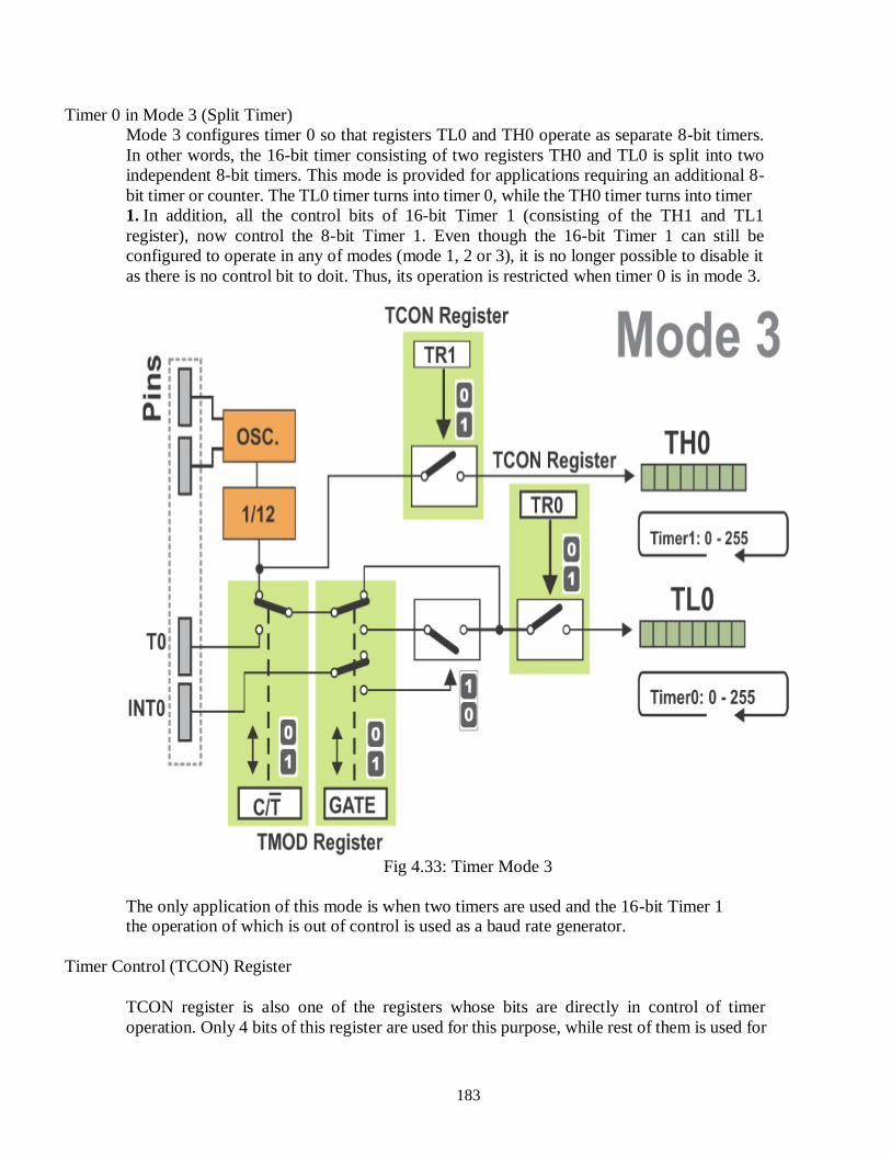
183
Timer 0 in Mode 3 (Split Timer)
Mode 3 configures timer 0 so that registers TL0 and TH0 operate as separate 8-bit timers.
In other words, the 16-bit timer consisting of two registers TH0 and TL0 is split into two
independent 8-bit timers. This mode is provided for applications requiring an additional 8-
bit timer or counter. The TL0 timer turns into timer 0, while the TH0 timer turns into timer
1. In addition, all the control bits of 16-bit Timer 1 (consisting of the TH1 and TL1
register), now control the 8-bit Timer 1. Even though the 16-bit Timer 1 can still be
configured to operate in any of modes (mode 1, 2 or 3), it is no longer possible to disable it
as there is no control bit to doit. Thus, its operation is restricted when timer 0 is in mode 3.
Fig 4.33: Timer Mode 3
The only application of this mode is when two timers are used and the 16-bit Timer 1 the operation of which is out of control is used as a baud rate generator.
Timer Control (TCON) Register
TCON register is also one of the registers whose bits are directly in control of timer
operation. Only 4 bits of this register are used for this purpose, while rest of them is used for
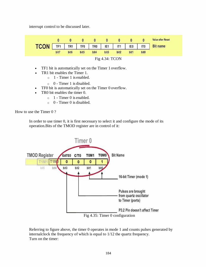
184
interrupt control to be discussed later.
Fig 4.34: TCON
TF1 bit is automatically set on the Timer 1 overflow.
TR1 bit enables the Timer 1.
o 1 - Timer 1 is enabled.
o 0 - Timer 1 is disabled. TF0 bit is automatically set on the Timer 0 overflow.
TR0 bit enables the timer 0.
o 1 - Timer 0 is enabled.
o 0 - Timer 0 is disabled.
How to use the Timer 0 ?
In order to use timer 0, it is first necessary to select it and configure the mode of its
operation.Bits of the TMOD register are in control of it:
Fig 4.35: Timer 0 configuration
Referring to figure above, the timer 0 operates in mode 1 and counts pulses generated by
internalclock the frequency of which is equal to 1/12 the quartz frequency.
Turn on the timer:
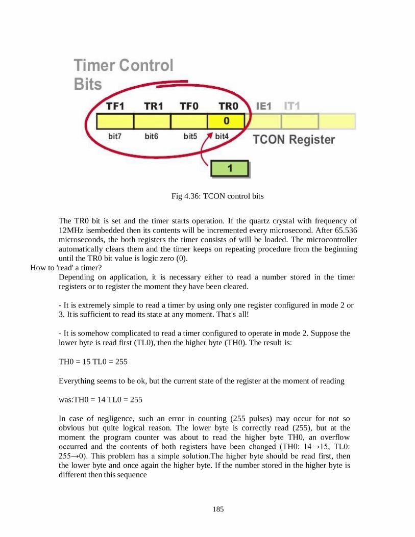
185
Fig 4.36: TCON control bits
The TR0 bit is set and the timer starts operation. If the quartz crystal with frequency of
12MHz isembedded then its contents will be incremented every microsecond. After 65.536
microseconds, the both registers the timer consists of will be loaded. The microcontroller
automatically clears them and the timer keeps on repeating procedure from the beginning
until the TR0 bit value is logic zero (0).
How to 'read' a timer?
Depending on application, it is necessary either to read a number stored in the timer
registers or to register the moment they have been cleared.
- It is extremely simple to read a timer by using only one register configured in mode 2 or 3. It is sufficient to read its state at any moment. That's all!
- It is somehow complicated to read a timer configured to operate in mode 2. Suppose the
lower byte is read first (TL0), then the higher byte (TH0). The result is:
TH0 = 15 TL0 = 255
Everything seems to be ok, but the current state of the register at the moment of reading
was:TH0 = 14 TL0 = 255
In case of negligence, such an error in counting (255 pulses) may occur for not so
obvious but quite logical reason. The lower byte is correctly read (255), but at the
moment the program counter was about to read the higher byte TH0, an overflow
occurred and the contents of both registers have been changed (TH0: 14→15, TL0:
255→0). This problem has a simple solution.The higher byte should be read first, then
the lower byte and once again the higher byte. If the number stored in the higher byte is
different then this sequence
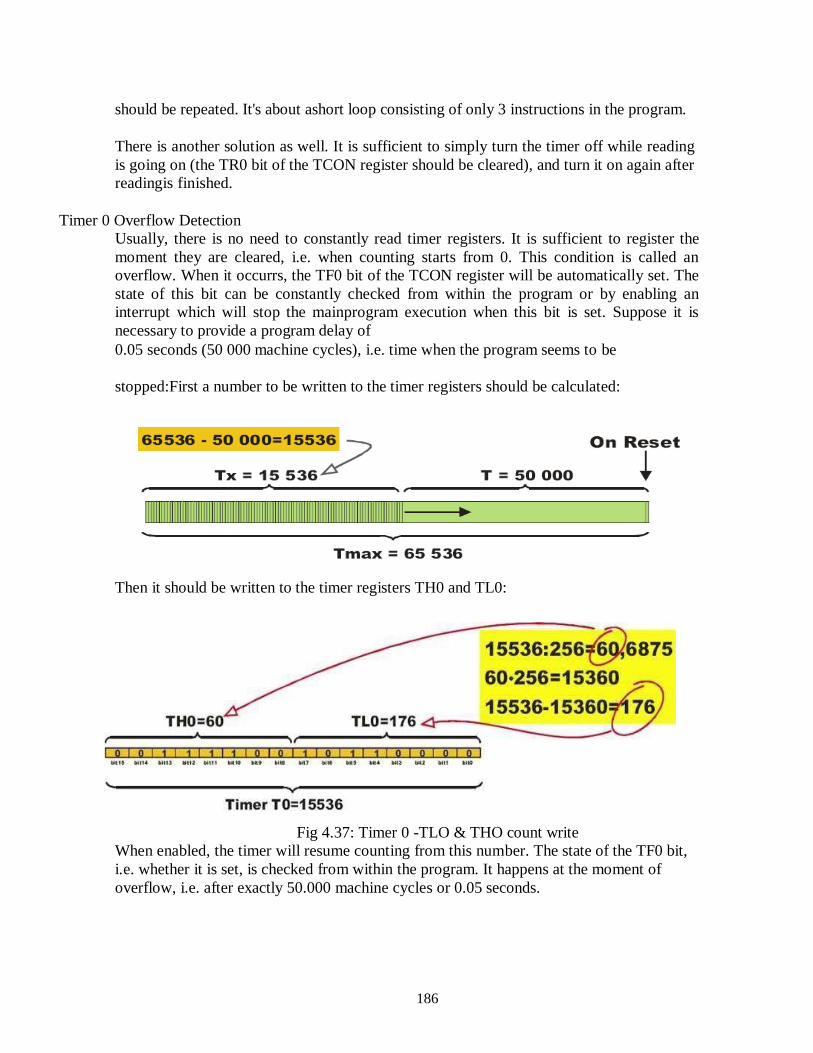
186
should be repeated. It's about ashort loop consisting of only 3 instructions in the program.
There is another solution as well. It is sufficient to simply turn the timer off while reading
is going on (the TR0 bit of the TCON register should be cleared), and turn it on again after
readingis finished.
Timer 0 Overflow Detection
Usually, there is no need to constantly read timer registers. It is sufficient to register the
moment they are cleared, i.e. when counting starts from 0. This condition is called an
overflow. When it occurrs, the TF0 bit of the TCON register will be automatically set. The
state of this bit can be constantly checked from within the program or by enabling an
interrupt which will stop the mainprogram execution when this bit is set. Suppose it is
necessary to provide a program delay of
0.05 seconds (50 000 machine cycles), i.e. time when the program seems to be
stopped:First a number to be written to the timer registers should be calculated:
Then it should be written to the timer registers TH0 and TL0:
Fig 4.37: Timer 0 -TLO & THO count write
When enabled, the timer will resume counting from this number. The state of the TF0 bit,
i.e. whether it is set, is checked from within the program. It happens at the moment of
overflow, i.e. after exactly 50.000 machine cycles or 0.05 seconds.

187
How to measure pulse duration?
Fig 4.38: Measure Pulse duration
Suppose it is necessary to measure the duration of an operation, for example how long a
device has been turned on? Look again at the figure illustrating the timer and pay attention
to the function of the GATE0 bit of the TMOD register. If it is cleared then the state of
the P3.2 pin doesn't affect timer operation. If GATE0 = 1 the timer will operate until the
pin P3.2 is cleared. Accordingly, if this pin is supplied with 5V through some external
switch at the moment the device is being turned on, the timer will measure duration of its
operation, which actually was the objective.
How to count up pulses?
Similarly to the previous example, the answer to this question again lies in the TCON
register. This time it's about the C/T0 bit. If the bit is cleared the timer counts pulses
generated by the internal oscillator, i.e. measures the time passed. If the bit is set, the timer
input is provided withpulses from the P3.4 pin (T0). Since these pulses are not always of
the same width, the timer cannot be used for time measurement and is turned into a
counter, therefore. The highest frequency that could be measured by such a counter is 1/24
frequency of used quartz-crystal.

188
Timer 1
Timer 1 is identical to timer 0, except for mode 3 which is a hold-count mode. It means
that theyhave the same function, their operation is controlled by the same registers TMOD
and TCON and both of them can operate in one out of 4 different modes.
Fig 4.39: timer 1
7.Serial Communication
One of the microcontroller features making it so powerful is an integrated UART, better
known as a serial port. It is a full-duplex port, thus being able to transmit and receive data
simultaneously and at different baud rates. Without it, serial data send and receive would be
an enormously complicated part of the program in which the pin state is constantly changed
and checked at regular intervals. When using UART, all the programmer has to do is to
simply selectserial port mode and baud rate. When it's done, serial data transmit is nothing
but writing to the SBUF register, while data receive represents reading the same register.
The microcontroller takescare of not making any error during data transmission.
Fig 4.40: SBUF
189
Serial port must be configured prior to being used. In other words, it is necessary to
determinehow many bits is contained in one serial ―word‖, baud rate and synchronization
clock source. The whole process is in control of the bits of the SCON register (Serial
Control).
Serial Port Control (SCON) Register
Fig 4.41: SCON
SM0 - Serial port mode bit 0 is used for serial port modeselection. SM1 - Serial port mode bit 1.
SM2 - Serial port mode 2 bit, also known as multiprocessor communication
enable bit. When set, it enables multiprocessor communication in mode 2 and 3,
and eventually mode 1. It should be cleared in mode 0.
REN - Reception Enable bit enables serial reception when set. When cleared,
serial reception is disabled.
TB8 - Transmitter bit 8. Since all registers are 8-bit wide, this bit solves the
problemof transmiting the 9th bit in modes 2 and 3. It is set to transmit a logic 1
in the 9th bit.
RB8 - Receiver bit 8 or the 9th bit received in modes 2 and 3. Cleared by
hardware if9th bit received is a logic 0. Set by hardware if 9th bit received is a
logic 1.
TI - Transmit Interrupt flag is automatically set at the moment the last bit of one
byte is sent. It's a signal to the processor that the line is available for a new byte
transmite. It must be cleared from within the software.
RI - Receive Interrupt flag is automatically set upon one byte receive. It signals
that byte is received and should be read quickly prior to being replaced by a new
data. This bit is also cleared from within the software.
As seen, serial port mode is selected by combining the SM0 and SM2 bits:
SM0 SM1 Mode Description Baud Rate
0 0 0 8-bit Shift Register 1/12 the quartz frequency
0 1 1 8-bit UART Determined by the timer 1
1 0 2 9-bit UART 1/32 the quartz frequency (1/64 the quartz frequency)
1 1 3 9-bit UART Determined by the timer 1

190
Fig 4.42: TXD , RXD
In mode 0, serial data are transmitted and received through the RXD pin, while the TXD pin
output clocks. The bout rate is fixed at 1/12 the oscillator frequency. On transmit, the least
significant bit (LSB bit) is sent/received first.
TRANSMIT - Data transmit is initiated by writing data to the SBUF register. In fact, this
process starts after any instruction being performed upon this register. When all 8 bits have
beensent, the TI bit of the SCON register is automatically set.
Fig 4.43: TXD , RXD status- TI-mode 0
189
RECEIVE - Data receive through the RXD pin starts upon the two following conditions
are met: bit REN=1 and RI=0 (both of them are stored in the SCON register). When all 8
bits havebeen received, the RI bit of the SCON register is automatically set indicating
that one byte receive is complete.
Fig 4.44: TXD , RXD-RI-mode 0
Since there are no START and STOP bits or any other bit except data sent from the SBUF
register in the pulse sequence, this mode is mainly used when the distance between devices
is short, noise is minimized and operating speed is of importance. A typical example is I/O
port expansion by adding a cheap IC (shift registers 74HC595, 74HC597 and similar).
Fig 4.45: TXD , RXD, SBUF,SCON-mode 1
190
In mode 1, 10 bits are transmitted through the TXD pin or received through the RXD pin
in thefollowing manner: a START bit (always 0), 8 data bits (LSB first) and a STOP bit
(always 1).
The START bit is only used to initiate data receive, while the STOP bit is automatically
writtento the RB8 bit of the SCON register.
TRANSMIT - Data transmit is initiated by writing data to the SBUF register. End
of datatransmission is indicated by setting the TI bit of the SCON register.
Fig 4.46: TXD , TI-mode 1
RECEIVE - The START bit (logic zero (0)) on the RXD pin initiates data receive. The
following two conditions must be met: bit REN=1 and bit RI=0. Both of them are stored
in theSCON register. The RI bit is automatically set upon data reception is complete.
Fig 4.47: RXD-RI-mode 1
The Baud rate in this mode is determined by the timer 1 overflow.
191
Mode 2
Fig 4.48: TXD , RXD-mode 2
In mode 2, 11 bits are transmitted through the TXD pin or received through the RXD pin:
a START bit (always 0), 8 data bits (LSB first), a programmable 9th data bit and a STOP
bit (always 1). On transmit, the 9th data bit is actually the TB8 bit of the SCON register.
This bit usually has a function of parity bit. On receive, the 9th data bit goes into the RB8
bit of the sameregister (SCON).The baud rate is either 1/32 or 1/64 the oscillator frequency.
TRANSMIT - Data transmit is initiated by writing data to the SBUF register. End
of datatransmission is indicated by setting the TI bit of the SCON register.
Fig 4.49: mode 2
RECEIVE - The START bit (logic zero (0)) on the RXD pin initiates data receive. The
following two conditions must be met: bit REN=1 and bit RI=0. Both of them are stored
in theSCON register. The RI bit is automatically set upon data reception is complete.

192
Fig 4.50: mode 2
Mode 3 is the same as Mode 2 in all respects except the baud rate. The baud rate in Mode
3 is variable.
Baud Rate
Baud Rate is a number of sent/received bits per second. In case the UART is used, baud
rate depends on: selected mode, oscillator frequency and in some cases on the state of the
SMOD bitof the SCON register. All the necessary formulas are specified in the table:
Timer 1 as a clock generator
Baud Rate Fosc. (MHz)
Bit SMOD
11.0592 12 14.7456 16 20
150 40 h 30 h 00 h 0
300 A0 h 98 h 80 h 75 h 52 h 0
600 D0 h CC h C0 h BB h A9 h 0
1200 E8 h E6 h E0 h DE h D5 h 0
2400 F4 h F3 h F0 h EF h EA h 0

193
4800 F3 h EF h EF h 1
4800 FA h F8 h F5 h 0
9600 FD h FC h 0
9600 F5 h 1
19200 FD h FC h 1
38400 FE h 1
76800 FF h 1
Multiprocessor Communication
As you may know, additional 9th data bit is a part of message in mode 2 and 3. It can be
used forchecking data via parity bit. Another useful application of this bit is in
communication between two or more microcontrollers, i.e. multiprocessor communication.
This feature is enabled by setting the SM2 bit of the SCON register. As a result, after
receiving the STOP bit, indicating end of the message, the serial port interrupt will be
generated only if the bit RB8 = 1 (the 9th bit).
This is how it looks like in practice:
Suppose there are several microcontrollers sharing the same interface. Each of them has its
own address. An address byte differs from a data byte because it has the 9th bit set (1),
while this bitis cleared (0) in a data byte. When the microcontroller A (master) wants to
transmit a block of data to one of several slaves, it first sends out an address byte which
identifies the target slave. An address byte will generate an interrupt in all slaves so that they
can examine the received byteand check whether it matches their address.
Fig 4.51: multiprocessor communication
Of course, only one of them will match the address and immediately clear the SM2 bit of
the SCON register and prepare to receive the data byte to come. Other slaves not being
addressed leave their SM2 bit set ignoring the coming data bytes.
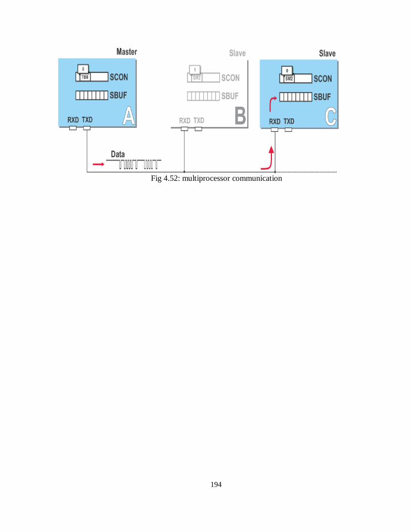
194
Fig 4.52: multiprocessor communication
195
QUESTION BANK
PART A
1. What are the addressing modes of 8051.
2. Differentiate microcontroller and microprocessor.
3. Write short notes on interrupts.
4. Write briefly about the timer of 8051.
5. What is an SFR.
6. List the SFR in 8051.
7. Write an assembly language program to transfer
8. a.10 data from internal to external
b.10 data from external to internal
9. Explain how to interface I/O devices to 8051. 10. Write a program to find a square of a number using look up table.10.Write a program to find the
given number is odd or even.
11. Write a program to generate a square wave of 1ms using timer.
12. List the bits of PSW.
13. What are the different ranges of jump.
14. Classify jump instruction
15. Write about stack
16. On reset the value of SP is , I/O ports are configured as .
17. Write about EA pin of 8051.
18. Draw one machine cycle of 8051.
19. What is ALE?
20. The internal RAM size is and the internal ROM size is .
PART B
1. With neat diagram explain the architecture of 8051.
2. Classify the instruction set of8051 and explain the instruction with suitable examples.
3. Write in detail how serial communication is carried out in 8051.
4. Explain in detail about timers in 8051 microcontroller
5. Explain the interrupts of 8051 microcontroller
6. Write the following programs
a. programs using arithmetic and logical instruction b. Programs to convert hexa to ascii and ascii to hexa
c. Programs using program transfer
instructions. d.Programs using I/O ports
7. Explain the following instructions with example
a. movc a,@a+dptr b. movx @r0,a c. JBC b,radd
d. XCHD A,@Rp e. Swap A

196
TEXT / REFERENCE BOOKS
1. Ramesh Gaonkar, ―Microprocessor Architecture, Programming and applications with 8085‖, 5th
Edition, Penram International Publishing Pvt Ltd, 2010. 2. Kenneth J Ayala, ―The 8051 Microcontroller‖, 2nd Edition, Thomson, 2005.
3. Nagoor Kani A, ―Microprocessor and Microcontroller‖, 2nd Edition, Tata McGraw Hill, 2012.
4. Mathur A.P. ‖ Introduction to microprocessor .―
5. Muhammad Ali Mazidi.‖The 8051 Microcontroller and Embedded Systems.‖
197
UNIT – V– MICROPROCESSORS AND MICROCONTROLLERS– SECA1601
SCHOOL OF ELECTRICAL AND ELECTRONICS
DEPARTMENT OF ELECTRONICS AND COMMUNICATION ENGINEERING

198
UNIT 5 APPLICATIONS BASED ON 8085 AND 8051
Interfacing Basic concepts, interfacing LED, 7 segment LED, Stepper motor control system,
Temperature control system, Traffic light control system, Motor speed control system, Waveform
generation, Interfacing LCD.
1. SEVEN SEGMENT LED
Fig 5.1: 7-sement LED types
• Fig shows two different type of 7-segment display; common cathode and common anode.
• 7-segment display consists of a few LEDs and are arranged physically as shown in figure a.
• It has seven segments from A to G that normally connected to data bus D0 to D6 respectively.
• If decimal point is used, D7 will be connected to DP; and left unconnected if it is unused.
Fig 5.2: 7-sement LED interfacing
• Fig. shows the example to interface seven segment display and address decoder with an address
of FDH.
• The common anode display is used therefore 0 logic is needed to activate the segment.
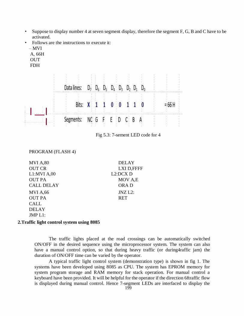
199
• Suppose to display number 4 at seven segment display, therefore the segment F, G, B and C have to be
activated.
• Follows are the instructions to execute it:
– MVI
A, 66H
OUT
FDH
Fig 5.3: 7-sement LED code for 4
PROGRAM (FLASH 4)
MVI A,80 DELAY
OUT CR LXI D,FFFF
L1:MVI A,00 L2:DCX D
OUT PA MOV A,E
CALL DELAY ORA D
MVI A,66 JNZ L2:
OUT PA RET
CALL
DELAY
JMP L1:
2.Traffic light control system using 8085
The traffic lights placed at the road crossings can be automatically switched
ON/OFF in the desired sequence using the microprocessor system. The system can also
have a manual control option, so that during heavy traffic (or during4raffic jam) the
duration of ON/OFF time can be varied by the operator.
A typical traffic light control system (demonstration type) is shown in fig 1. The
systems have been developed using 8085 as CPU. The system has EPROM memory for
system program storage and RAM memory for stack operation. For manual control a
keyboard have been provided. It will be helpful for the operator if the direction 6ftraffic flow
is displayed during manual control. Hence 7-segment LEDs are interfaced to display the

200
direction of traffic flow both during manual and automatic mode.
The primary function of the microprocessor in the system is to switch ON/OFF the
Red/Yellow/Green lights is the specified sequence. In the demonstration system of fig,
Red/Yellow/Green LEDs are provided instead of lights (lamps). The LEDs are interfaced
to the system through buffer (74LS245) and ports of 8255.
In the practical implementation scheme the lights can be turned ON/OFF using driver
transistors and relays. In practical implementation the output of buffer (74LS245) can be
connected to the driver transistor. A reverse biased diode is connected across relay coil to
prevent relay chattering (for free-wheeling action).
The microprocessor send High through a port line to switch ON the light and LOW
to switch OFF the light. A switching schedule (or sequence) can be developed as shown in
Table. In this switching sequence it is assumed that the traffic is allowed only in one
direction at time.
In table, "1" represents ON condition and "0" represents OFF condition. These 1's and O's
Can be directly output to 8255 ports to switch ON/OFF the light. A flowchart for
traffic lightcontrol program is shown in fig .
Fig.5.4: 8085 Microprocessor based Traffic light control system.
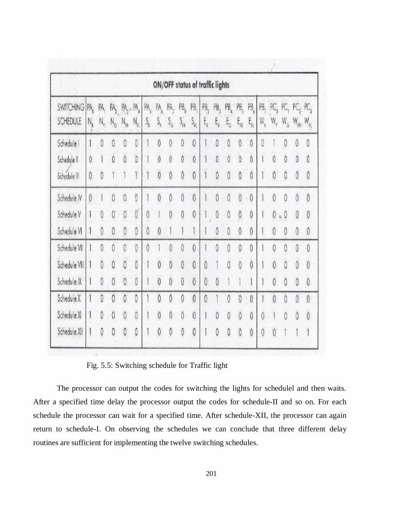
201
Fig. 5.5: Switching schedule for Traffic light
The processor can output the codes for switching the lights for schedulel and then waits.
After a specified time delay the processor output the codes for schedule-II and so on. For each
schedule the processor can wait for a specified time. After schedule-XII, the processor can again
return to schedule-I. On observing the schedules we can conclude that three different delay
routines are sufficient for implementing the twelve switching schedules.
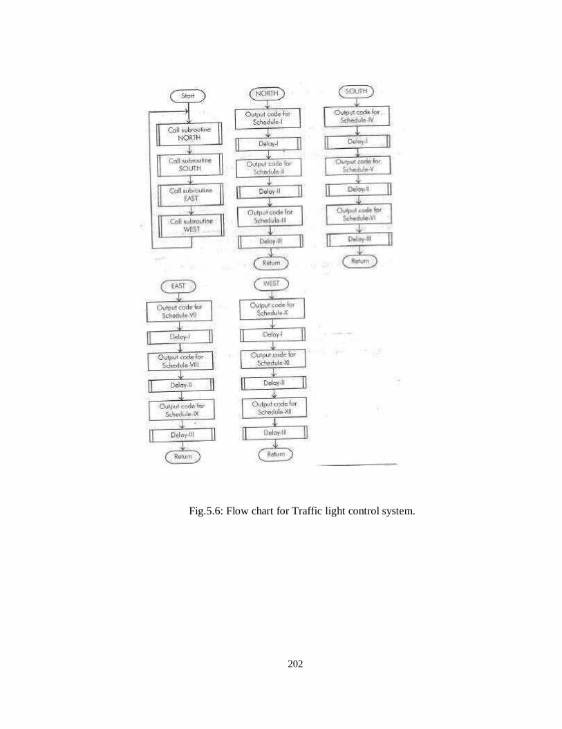
202
Fig.5.6: Flow chart for Traffic light control system.

203
3.Temperature controller using 8085
The microprocessor based temperature control system can be used for automatic
control of the temperature of a body. A simplified block diagram of 8085 microprocessor
based temperature control system is shown in fig 4 . The system consist of 8085
microprocessor as CPU, ERROM&RAM memory for program & data storage, INTEL 8279
for keyboard and display Interface, ADC, DAC, INTEL 8255 for I/O' ports, Amplifiers,
Signal conditioning circuit, Temperature sensor and Supply control circuit. In this system
the temperature is controlled by controlling the power input to the heating element.
The temperature of the body is measured using a temperature sensor. The different
types of temperature sensor that can be used for temperature measurement are Thermo-
couple, Thermistors , PN-junctions, IC sensors. This sensor will convert the input
temperature to Proportional analog voltage or current. The output signal of the sensor will
be a weak signal and so has to be amplified by using high input impedance op-amp. Then
the analog signal is scaled tosuitable level by the signal conditioning circuit.
The microprocessor can process only digital signals and so the analog signal from signal
conditioning circuit cannot be read by the processor directly. The system has an analog-to-
digital converter (ADC) to convert the analog signal to proportional digital data. In this
system the ADC is interfaced to 8085 processor through port-A of 8255. The 8085
processor send signal to ADC to start conversion and at the end of conversion it read the
digital data from the port-A of8255.
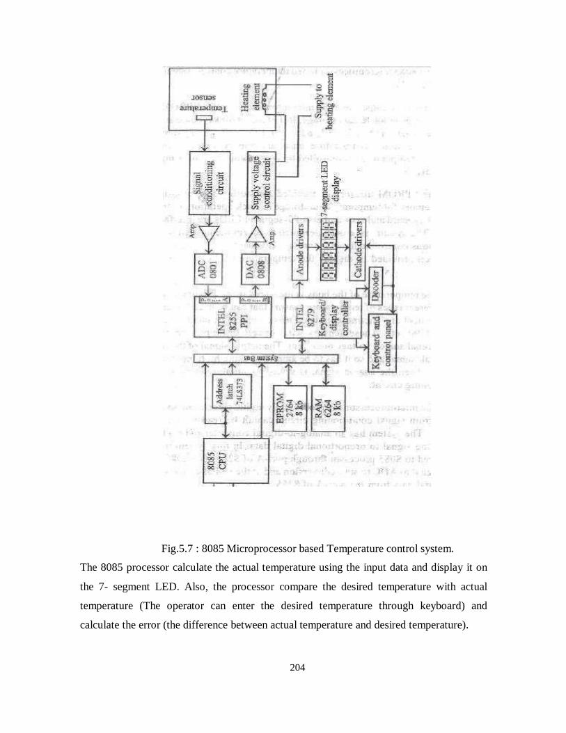
204
Fig.5.7 : 8085 Microprocessor based Temperature control system.
The 8085 processor calculate the actual temperature using the input data and display it on
the 7- segment LED. Also, the processor compare the desired temperature with actual
temperature (The operator can enter the desired temperature through keyboard) and
calculate the error (the difference between actual temperature and desired temperature).

Fig.5.8: Flow chart for Temperature control system.
The error is used to compute a digital control signal, which is converted to analog control
signal by DAC. The DAC is interfaced to the system through port-B of 8255. The analog
control signal produced by DAC is used to control the power supply of the heating element
of the body.

The digital control signal can be computed by the 8085 processor using different
digitalcontrol algorithms (PIPI/PID/FUZZY logic control algorithms).
The control circuit for power supply can be either thyristor based circuit or relay. In case of
thyristor control circuits the firing angle can be varied by the control signal to control the
power input to the heater.
4.Stepper motor controller system using 8085
The stepper motors are popularly used in computer peripherals, plotters, robots and
machine tools for 'precise incremental rotation. In stepper motor, the stator windings are
excited by electrical pulses and for each pulse the motor shaft advances by one angular step.
(Single the stepper motor can be driven by digital pulses; it is also called digital motor).
The step size in the motor is determined by the number of poles in the rotor and the number
'of pairs of stator windings (one pair of stator winding is called one 'phase). The stator
windings are also called control windings.
The motor is controlled by switching ON/OFF the control winding. The popular
stepper motor used for demonstration in laboratories has a step size of 1.8° (i.e, 200 steps
per revolution). This motor consist of four stator winding and require four switching
sequence as shown in table 1. The basic step size of the motor is called full-step. By
altering the switching sequence, the motor can be made to run with incremental motion of
half the full-step value.
A typical stepper motor control system is shown in fig 6. a two-phase or four winding
stepper motor is show in fig 6. The system consists of 8085 microprocessor as CPU,
EPROM and RAM memory for program &data storage and for stack. Using INTEL 8279,
a keyboard and six number of 7-segment LED display has been interfaced in the system.
Through the keyboard the operator can issue commands to control the system. The LED
display has been provided to display messages to the operator. The windings of stepper
motor connected to the collector of Darlington pair transistors. The transistors are switched
ON/OFF by the microprocessor through the ports of 8255 and buffer (74LS245). A free
wheeling diode is connected across each windingfor fast switching. The flowchart for the
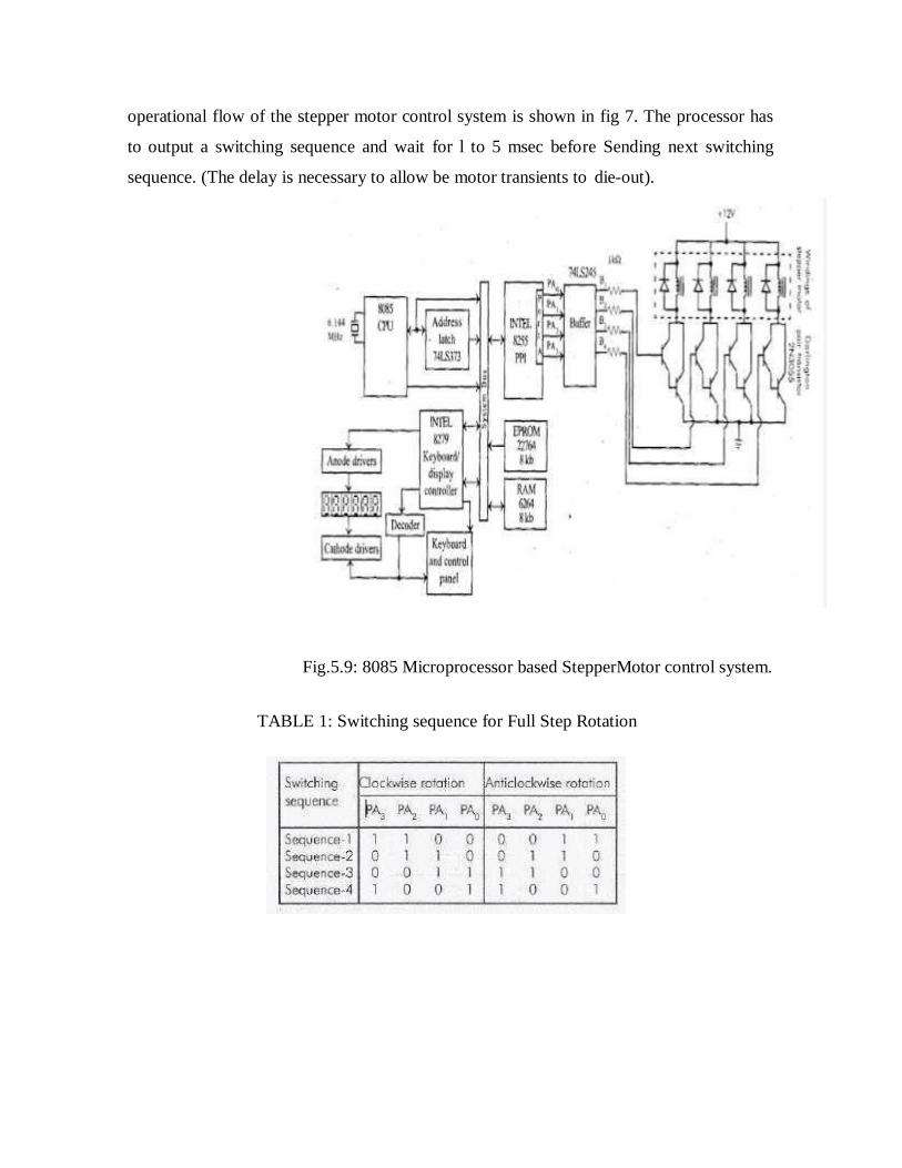
operational flow of the stepper motor control system is shown in fig 7. The processor has
to output a switching sequence and wait for l to 5 msec before Sending next switching
sequence. (The delay is necessary to allow be motor transients to die-out).
Fig.5.9: 8085 Microprocessor based StepperMotor control system.
TABLE 1: Switching sequence for Full Step Rotation

210
Fig.5.10: Flow chart for Stepper motor control system.
5.Interfacing Stepper Motor with 8051
The Stepper Motor to microcontroller. As you can see the stepper motor is connected
with Microcontroller output port pins through a ULN2803A array. So when the
microcontroller is giving pulses with particular frequency to ls293A, the motor is rotated
in clockwise or anticlockwise. Fig. Interfacing Stepper Motor to Microcontroller
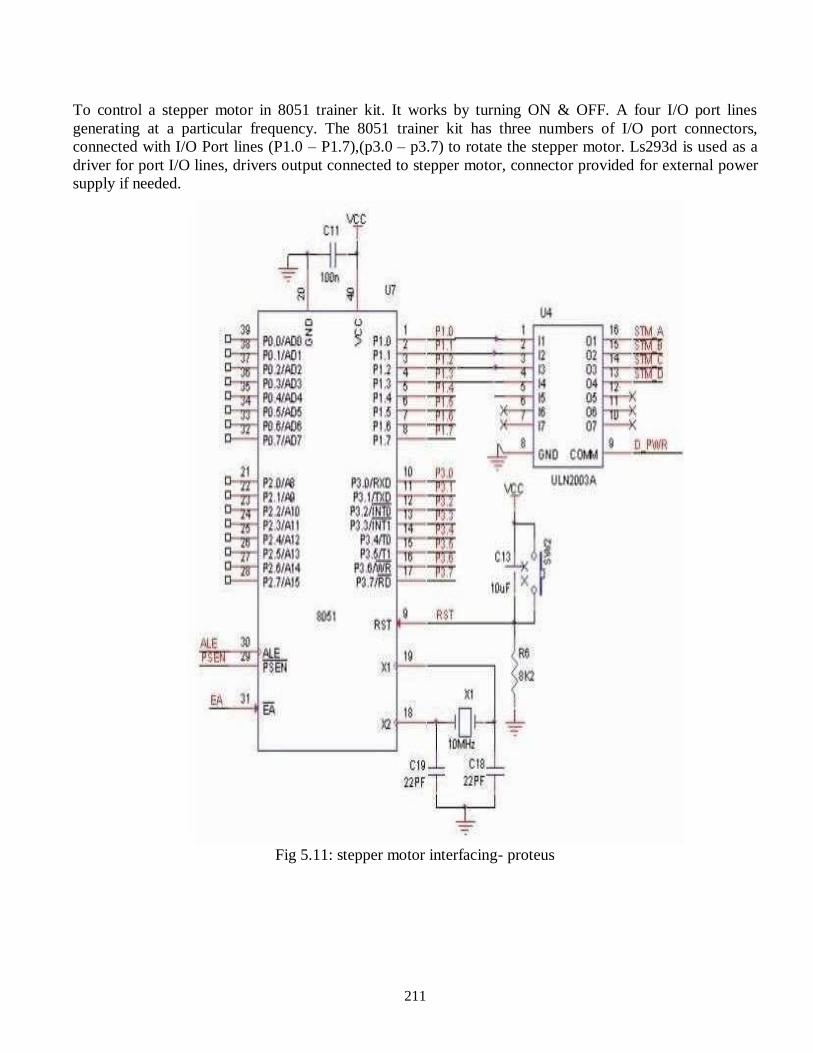
211
To control a stepper motor in 8051 trainer kit. It works by turning ON & OFF. A four I/O port lines
generating at a particular frequency. The 8051 trainer kit has three numbers of I/O port connectors,
connected with I/O Port lines (P1.0 – P1.7),(p3.0 – p3.7) to rotate the stepper motor. Ls293d is used as a
driver for port I/O lines, drivers output connected to stepper motor, connector provided for external power
supply if needed.
Fig 5.11: stepper motor interfacing- proteus
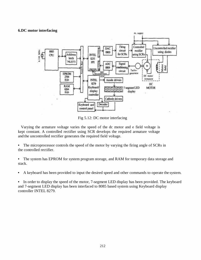
212
6.DC motor interfacing
Fig 5.12: DC motor interfacing
Varying the armature voltage varies the speed of the dc motor and e field voltage is
kept constant. A controlled rectifier using SCR develops the required armature voltage
and the uncontrolled rectifier generates the required field voltage.
• The microprocessor controls the speed of the motor by varying the firing angle of SCRs in
the controlled rectifier.
• The system has EPROM for system program storage, and RAM for temporary data storage and
stack.
• A keyboard has been provided to input the desired speed and other commands to operate the system.
• In order to display the speed of the motor, 7-segment LED display has been provided. The keyboard
and 7-segment LED display has been interfaced to 8085 based system using Keyboard display
controller INTEL 8279.
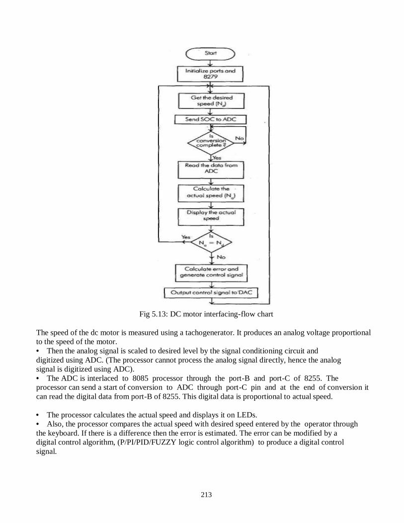
213
Fig 5.13: DC motor interfacing-flow chart
The speed of the dc motor is measured using a tachogenerator. It produces an analog voltage proportional
to the speed of the motor.
• Then the analog signal is scaled to desired level by the signal conditioning circuit and
digitized using ADC. (The processor cannot process the analog signal directly, hence the analog
signal is digitized using ADC).
• The ADC is interlaced to 8085 processor through the port-B and port-C of 8255. The
processor can send a start of conversion to ADC through port-C pin and at the end of conversion it
can read the digital data from port-B of 8255. This digital data is proportional to actual speed.
• The processor calculates the actual speed and displays it on LEDs.
• Also, the processor compares the actual speed with desired speed entered by the operator through
the keyboard. If there is a difference then the error is estimated. The error can be modified by a
digital control algorithm, (P/PI/PID/FUZZY logic control algorithm) to produce a digital control
signal.
214
• The digital control signal is converted to analog signal by the DAC. The analog signal is used
to alter the firing angle of SCRS in the controlled rectifiers. The operational the speed control system is
shown in the flowchart.
WAVE FORM
GENERATION L1:SETB
90
LCALL DELAY CLR 90
LCALL
DELAY
SJMP L1:
DELA
Y MOV
R0,#33
L2:DJNZ
R0,L2 RET
Connect the positive of the CRO to
P1.0 Gnd to gnd
Set the bit, call delay so that the on time also depends on the delay
Clear the bit, call delay so that the off time also depends on the
delay
Steps to generate a square wave using 8051
1. Set the output of any port on the 8051 to logic high.
2. Wait for some time.
3. Set the output of the same port to logic low.
4. Again wait for the same amount of time as done earlier.
5. Loop around the same.
Subsequently, for obtaining the desired frequency on the square wave. We have to manipulate with the
delay. We know that the machine cycle frequency is 1/12 of the crystal oscillator frequency. So, with the
crystal oscillator‘s frequency as 11.0592 Mhz the machine cycle frequency is 921.6 Khz. To sum up, thats
equivalent to 1.085 μsecond.
To generate a square wave of 1 KHz, in other words, a wave of time period 1 millisecond, we have to use
the delay in such a way that it causes a delay of 1 millisecond. We will have to loop around doing nothing
for about 461 machine cycles to generate a square wave of 50% duty cycle. That is to say, an on time and
an off time of 0.5 millisecond.
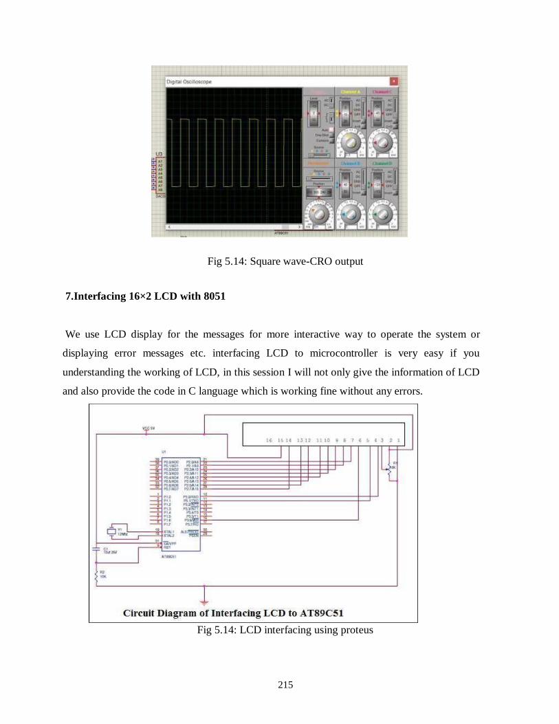
215
Fig 5.14: Square wave-CRO output
7.Interfacing 16×2 LCD with 8051
We use LCD display for the messages for more interactive way to operate the system or
displaying error messages etc. interfacing LCD to microcontroller is very easy if you
understanding the working of LCD, in this session I will not only give the information of LCD
and also provide the code in C language which is working fine without any errors.
Fig 5.14: LCD interfacing using proteus
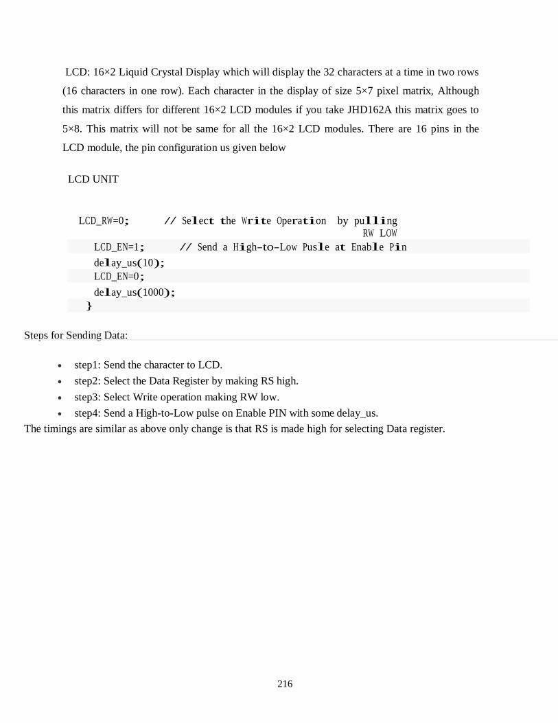
216
LCD: 16×2 Liquid Crystal Display which will display the 32 characters at a time in two rows
(16 characters in one row). Each character in the display of size 5×7 pixel matrix, Although
this matrix differs for different 16×2 LCD modules if you take JHD162A this matrix goes to
5×8. This matrix will not be same for all the 16×2 LCD modules. There are 16 pins in the
LCD module, the pin configuration us given below
LCD UNIT
LCD_RW=0; // Select the Write Operation by pulling
RW LOW
LCD_EN=1; // Send a High-to-Low Pusle at Enable Pin
delay_us(10);
LCD_EN=0;
delay_us(1000);
}
Steps for Sending Data:
step1: Send the character to LCD.
step2: Select the Data Register by making RS high.
step3: Select Write operation making RW low.
step4: Send a High-to-Low pulse on Enable PIN with some delay_us.
The timings are similar as above only change is that RS is made high for selecting Data register.

217
HARDWARE CONNECTION
Fig 5.16: LCD interfacing-hardware

218
QUESTION BANK
PART A
1. What are the two types of seven segment LED
2. Draw the schematic of 7 segment LED
3. Stepper motor interfaced to 8085. How?
4. Write 7 segment common cathode and anode code for displaying ‗E‘
5. Write the traffic light schedule for N-G, S-R, E-R, W-R and NFL & NFR- ON
6. Write the stepping sequence for stepper motor
7. What is the drawback of LCD
8. Write a program to generate square wave using 8051
9. Compare 7-segment LED and LCD
10. How the speed of the motor can be varied
11. List the applications of Stepper motor
PART B
1. Explain how the 7-segment LED is interfaced to 8085/8051
2. With neat diagram explain the stepper motor interfacing
3. Discuss in detail about temperature control system
4. Explain motor speed control system with necessary diagram
5. Discuss in detail about LCD interfacing with 8051
6. Interface traffic light controller to 8085/8051 and control the traffic.
TEXT / REFERENCE BOOKS
1. Ramesh Gaonkar, ―Microprocessor Architecture, Programming and applications with 8085‖, 5th
Edition, Penram International Publishing Pvt Ltd, 2010. 2. Kenneth J Ayala, ―The 8051 Microcontroller‖, 2nd Edition, Thomson, 2005.
3. Nagoor Kani A, ―Microprocessor and Microcontroller‖, 2nd Edition, Tata McGraw Hill, 2012.
4. Mathur A.P. ‖ Introduction to microprocessor .―
5. Muhammad Ali Mazidi.‖The 8051 Microcontroller and Embedded Systems.‖


