Embed Size (px)
Citation preview
Computers and Electrical Engineering 35 (2009) 258–285
Contents lists available at ScienceDirect
Computers and Electrical Engineering
journal homepage: www.elsevier .com/ locate /compeleceng
Resource management and task partitioning and scheduling on a run-timereconfigurable embedded system
Radha Guha *, Nader Bagherzadeh, Pai ChouEECS Department of UC, Irvine, United States
a r t i c l e i n f o
Article history:Available online 5 August 2008
Keywords:HW/SW co-designStreaming applicationsApplication convergenceHardware resource managementTask placementPartitioning and scheduling algorithm
0045-7906/$ - see front matter � 2008 Elsevier Ltddoi:10.1016/j.compeleceng.2008.06.008
* Corresponding author.E-mail addresses: [email protected] (R. Guha), nade
a b s t r a c t
There are many design challenges in the hardware-software co-design approach for perfor-mance improvement of data-intensive streaming applications with a general-purposemicroprocessor and a hardware accelerator. These design challenges are mainly to preventhardware area fragmentation to increase resource utilization, to reduce hardware reconfig-uration cost and to partition and schedule the tasks between the microprocessor and thehardware accelerator efficiently for performance improvement and power savings of theapplications.
In this paper a modular and block based hardware configuration architecture namedmemory-aware run-time reconfigurable embedded system (MARTRES) is proposed for effi-cient resource management and performance improvement of streaming applications.Subsequently we design a task placement algorithm named hierarchical best fit ascending(HBFA) algorithm to prove that MARTRES configuration architecture is very efficient inincreased resource utilization and flexible in task mapping and power savings. The timecomplexity of HBFA algorithm is reduced to O(n) compared to traditional Best Fit (BF) algo-rithm’s time complexity of O(n2), when the quality of the placement solution by HBFA isbetter than that of BF algorithm. Finally we design an efficient task partitioning and sched-uling algorithm named balanced partitioned and placement-aware partitioning and sched-uling algorithm (BPASA). In BPASA we exploit the temporal parallelism in streamingapplications to reduce reconfiguration cost of the hardware, while keeping in mind therequired throughput of the output data. We balance the exploitation of spatial parallelismand temporal parallelism in streaming applications by considering the reconfiguration costvs. the data transfer cost. The scheduler refers to the HBFA placement algorithm to checkwhether contiguous area on FPGA is available before scheduling the task for HW or for SW.
� 2008 Elsevier Ltd. All rights reserved.
1. Introduction
Tremendous amount of streaming data is generated as a result of various experiments and observations in the scientificfield of biology, physics, astronomy, human genome etc. Huge amount of data is also collected by various medical devicesand air and space-borne radar systems etc. Relatively small size algorithms work on these voluminous data to perform taskswith real-time simulation needs. Computational loads generally range from 10 MOPs (mega operations) for lightweightaudio processing to 3 GOPs (giga operations) for video processing to 20 GOPs for multilingual conversation interfaces andup to 1 TOPs (tera operations) for synthetic video generation [1]. Performing these tasks by CPU, which works sequentiallyand has no way of exploiting data level and control level parallelism takes a long time. Whereas on synchronous random
. All rights reserved.
[email protected] (N. Bagherzadeh), [email protected] (P. Chou).
R. Guha et al. / Computers and Electrical Engineering 35 (2009) 258–285 259
access memory (SRAM) based field programmable gate arrays (FPGAs), many parallel processors can be configured for pro-cessing these voluminous data concurrently, reducing the overall execution time of the application and increasing thethroughput of output data. As the best possible parallel architecture for a specific application is configured on FPGA staticallyor dynamically several times during the run-time of an application, scope of performance improvement, power efficiencyand resource utilization of the FPGA hardware for single or multiple algorithms running simultaneously on the same chipis very high. Apart from the parallel processing and reconfiguration capabilities of FPGAs, its lower design cost and shortertime-to-market make it a popular technology for embedded system development in contrast to the application specific inte-grated circuits (ASICs).
Several streaming applications such as fast Fourier transform (FFT), discrete Cosine transform (DCT) and data encryptionstandard (DES) etc. require data-intensive computations, real-time processing and high-bandwidth data transfer from exter-nal memory to on-chip memory. Hundred percent of an algorithm cannot always be parallelized. The data intensive com-putations of the streaming applications can be accelerated by the FPGA’s concurrent processors and the remainingcontrol intensive parts are better suited for general-purpose microprocessor for running sequentially.
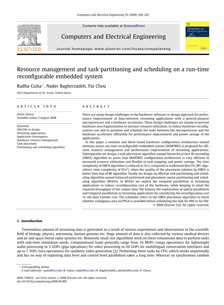
These kind of streaming applications need a general-purpose processor for hosting a real-time operating system (RTOS)for configuration, resource management and task scheduling on hardware. A block diagram of the required hybrid system isshown in Fig. 1. When the general-purpose microprocessor does most of the control work, the reconfigurable logic fabric is incharge of processing data of compute intensive functions and accelerating the critical sections of an algorithm.
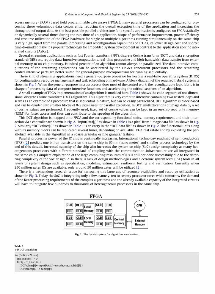
A small example of FPGA implementation of an algorithm is modeled here. Table 1 shows the code segment of one dimen-sional discrete Cosine transform (DCT) algorithm. This algorithm is very compute intensive containing two nested loops andserves as an example of a procedure that is sequential in nature, but can be easily parallelized. DCT algorithm is block basedand can be divided into smaller blocks of 8�8 pixel sizes for parallel execution. In DCT, multiplications of image data by a setof cosine values are performed. Frequently used, fixed set of cosine values can be kept in an on-chip read only memory(ROM) for faster access and thus can contribute to the speedup of the algorithm.
This DCT algorithm is mapped onto FPGA and the corresponding functional units, memory requirement and their inter-action via a controller are shown in Fig. 2. ‘‘inputData[j]” as shown in Table 1 is a pixel from ‘‘Image data file” as shown in Fig.2. Similarly ‘‘DCTvalues[i]” as shown in Table 1 is an entry in the ‘‘DCT data file” as shown in Fig. 2. The functional units alongwith its memory blocks can be replicated several times, depending on available FPGA real estate and by exploiting the par-allelism available in the algorithm in a coarse granular or fine granular fashion.
Parallel processing power of the IC chip is continually increasing. International technology roadmap of semiconductors(ITRS) [2] predicts one billion transistors on the same chip in 65 nm (nano meter) and smaller process technology by theend of this decade. Increased capacity of the chip also increases the system on chip (SoC) design complexity as many het-erogeneous processors with different standard of coupling with the communication infrastructure are all integrated inthe same chip. Complete exploitation of the large computing resources of ICs is still not done successfully due to the deter-ring complexity of the SoC design. Also there is lack of design methodologies and electronic system level (ESL) tools in alllevels of system design such as specification, modeling, estimation, synthesis, testing and verification. Currently when250 million gates ICs are available, only around 50 million gates will be utilized [3].
There is a tremendous research scope for narrowing this large gap of resource availability and resource utilization asshown in Fig. 3. Today the SoC is integrating only a few, namely, ten to twenty processor cores while tomorrow the demandof the faster processing requirements of the complex algorithms and the already available capacity of the integrated circuitswill have to integrate few hundreds to thousands of heterogeneous processors in the same chip.
Fig. 1. The hybrid system for algorithm acceleration.
Table 11-D DCT algorithm
for (i = 0; i < N; i++){DCTvalues[i] = 0;for (j = 0; j < N; j++)
{DCTvalues[i]+=inputData[j]�encode_cos_table[i][j];}DCTvalues[i]� = c_table[i];}
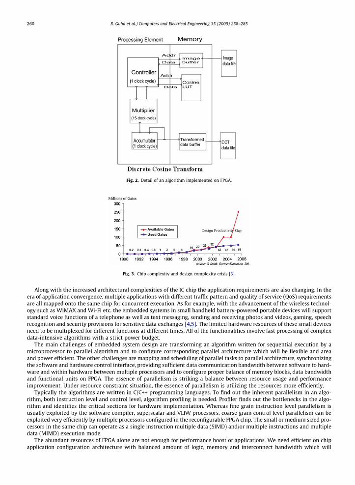
Fig. 2. Detail of an algorithm implemented on FPGA.
Fig. 3. Chip complexity and design complexity crisis [3].
260 R. Guha et al. / Computers and Electrical Engineering 35 (2009) 258–285
Along with the increased architectural complexities of the IC chip the application requirements are also changing. In theera of application convergence, multiple applications with different traffic pattern and quality of service (QoS) requirementsare all mapped onto the same chip for concurrent execution. As for example, with the advancement of the wireless technol-ogy such as WiMAX and Wi-Fi etc. the embedded systems in small handheld battery-powered portable devices will supportstandard voice functions of a telephone as well as text messaging, sending and receiving photos and videos, gaming, speechrecognition and security provisions for sensitive data exchanges [4,5]. The limited hardware resources of these small devicesneed to be multiplexed for different functions at different times. All of the functionalities involve fast processing of complexdata-intensive algorithms with a strict power budget.
The main challenges of embedded system design are transforming an algorithm written for sequential execution by amicroprocessor to parallel algorithm and to configure corresponding parallel architecture which will be flexible and areaand power efficient. The other challenges are mapping and scheduling of parallel tasks to parallel architecture, synchronizingthe software and hardware control interface, providing sufficient data communication bandwidth between software to hard-ware and within hardware between multiple processors and to configure proper balance of memory blocks, data bandwidthand functional units on FPGA. The essence of parallelism is striking a balance between resource usage and performanceimprovement. Under resource constraint situation, the essence of parallelism is utilizing the resources more efficiently.
Typically the algorithms are written in C/C++ programming languages. To find out the inherent parallelism in an algo-rithm, both instruction level and control level, algorithm profiling is needed. Profiler finds out the bottlenecks in the algo-rithm and identifies the critical sections for hardware implementation. Whereas fine grain instruction level parallelism isusually exploited by the software compiler, superscalar and VLIW processors, coarse grain control level parallelism can beexploited very efficiently by multiple processors configured in the reconfigurable FPGA chip. The small or medium sized pro-cessors in the same chip can operate as a single instruction multiple data (SIMD) and/or multiple instructions and multipledata (MIMD) execution mode.
The abundant resources of FPGA alone are not enough for performance boost of applications. We need efficient on chipapplication configuration architecture with balanced amount of logic, memory and interconnect bandwidth which will
R. Guha et al. / Computers and Electrical Engineering 35 (2009) 258–285 261
provide concurrency, flexibility, scalability, power and performance efficiency and better resource utilization for the SIMDand MIMD application execution modes.
The configuration architecture also has to be flexible for task mapping and modular for partial run-time reconfigurationand for power savings by advanced technologies like clock gating, voltage scaling etc. on a particular region. All the SoC de-sign issues such as wire delay, power management, embedded software, IP integration, signal integrity, RF effects can be bet-ter handled with a modular architecture which is more flexible for reconfiguration and for other control issues. We also needefficient resource manager and task scheduling algorithm which will be fast in mapping a dynamic task list and also providea compact task mapping solution and faster application execution solution. A modular and flexible application configurationarchitecture having better resource utilization is the key to power savings, increased multi-tasking capabilities and overallperformance improvement of the applications.
Thus we have designed a modular and block based flexible configuration architecture for FPGA, named memory-awarerun-time reconfigurable embedded system (MARTRES) which will facilitate partial reconfiguration at run-time, efficient re-source management and resource utilization by our hierarchical best fit ascending (HBFA) task placement algorithm and bal-anced partitioned and placement-aware partitioning and scheduling algorithm (BPASA). In this paper, we focus on hardwareresource management between a number of competing tasks in the order they arrive or the tasks which have already beenidentified for concurrent hardware execution. On the contrary in Refs. [6,7], their partitioning and scheduling algorithmsevaluate many task parameters for task ordering before the actual task placement.
Before we explore the related work on reconfigurable computing platform we introduce the target hardware architectureof modern FPGA devices, its system integration support and shortcomings for application acceleration.
1.1. FPGA architecture
FPGA is a semi-conducting device with programmable configurable logic blocks (CLBs), input–output blocks (IOBs), blockrandom access memory (BRAM), interconnects, clock resources and configuration circuitry [8–11]. CLBs are lookup table(LUT) based where a k-input LUT can store any logic function of k-binary variables. The inter connections between the CLBsare a two dimensional network of connectors and routers called connection network. There is also provision for temporaryon-chip data storage, as all computations require data. An array of CLBs on FPGA is surrounded by a number of IOBs for datatransfer to and from external memory. LUT-based FPGA stores logic functions and the configuration bits that drive theswitching matrix of the FPGA. Modern FPGAs also provide fast and dedicated ASIC quality arithmetic operation units suchas multiply and accumulate (MAC) units as DSP blocks for computation intensive algorithms. The CLBs, IOBs, DSPs andBRAMs are all run-time reprogrammable on the order of milliseconds to create an efficient interface between the logicdata-path and the memory.
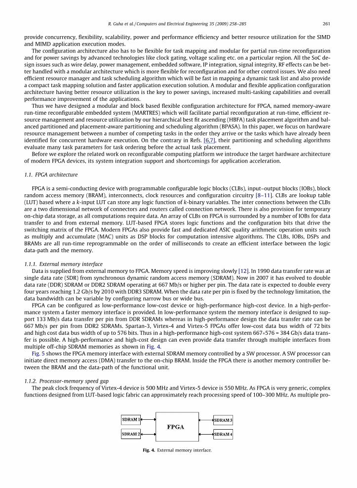
1.1.1. External memory interfaceData is supplied from external memory to FPGA. Memory speed is improving slowly [12]. In 1990 data transfer rate was at
single data rate (SDR) from synchronous dynamic random access memory (SDRAM). Now in 2007 it has evolved to doubledata rate (DDR) SDRAM or DDR2 SDRAM operating at 667 Mb/s or higher per pin. The data rate is expected to double everyfour years reaching 1.2 Gb/s by 2010 with DDR3 SDRAM. When the data rate per pin is fixed by the technology limitation, thedata bandwidth can be variable by configuring narrow bus or wide bus.
FPGA can be configured as low-performance low-cost device or high-performance high-cost device. In a high-perfor-mance system a faster memory interface is provided. In low-performance system the memory interface is designed to sup-port 133 Mb/s data transfer per pin from DDR SDRAMs whereas in high-performance design the data transfer rate can be667 Mb/s per pin from DDR2 SDRAMs. Spartan-3, Virtex-4 and Virtex-5 FPGAs offer low-cost data bus width of 72 bitsand high cost data bus width of up to 576 bits. Thus in a high-performance high-cost system 667�576 = 384 Gb/s data trans-fer is possible. A high-performance and high-cost design can even provide data transfer through multiple interfaces frommultiple off-chip SDRAM memories as shown in Fig. 4.
Fig. 5 shows the FPGA memory interface with external SDRAM memory controlled by a SW processor. A SW processor caninitiate direct memory access (DMA) transfer to the on-chip BRAM. Inside the FPGA there is another memory controller be-tween the BRAM and the data-path of the functional unit.
1.1.2. Processor-memory speed gapThe peak clock frequency of Virtex-4 device is 500 MHz and Virtex-5 device is 550 MHz. As FPGA is very generic, complex
functions designed from LUT-based logic fabric can approximately reach processing speed of 100–300 MHz. As multiple pro-
Fig. 4. External memory interface.
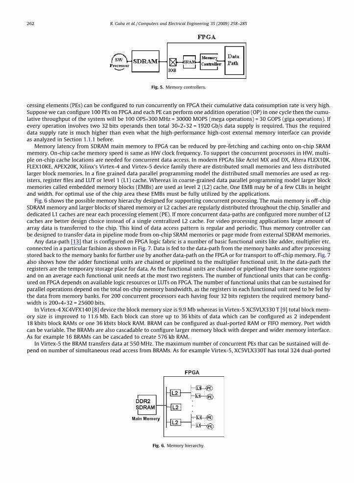
Fig. 5. Memory controllers.
262 R. Guha et al. / Computers and Electrical Engineering 35 (2009) 258–285
cessing elements (PEs) can be configured to run concurrently on FPGA their cumulative data consumption rate is very high.Suppose we can configure 100 PEs on FPGA and each PE can perform one addition operation (OP) in one cycle then the cumu-lative throughput of the system will be 100 OPS�300 MHz = 30000 MOPS (mega operations) = 30 GOPS (giga operations). Ifevery operation involves two 32 bits operands then total 30�2�32 = 1920 Gb/s data supply is required. Thus the requireddata supply rate is much higher than even what the high-performance high-cost external memory interface can provideas analyzed in Section 1.1.1 before.
Memory latency from SDRAM main memory to FPGA can be reduced by pre-fetching and caching onto on-chip SRAMmemory. On-chip cache memory speed is same as HW clock frequency. To support the concurrent processors in HW, multi-ple on-chip cache locations are needed for concurrent data access. In modern FPGAs like Actel MX and DX, Altera FLEX10K,FLEX10KE, APEX20K, Xilinx’s Virtex-4 and Virtex-5 device family there are distributed small memories and less distributedlarger block memories. In a fine grained data parallel programming model the distributed small memories are used as reg-isters, register files and LUT or level 1 (L1) cache. Whereas in coarse-grained data parallel programming model larger blockmemories called embedded memory blocks (EMBs) are used as level 2 (L2) cache. One EMB may be of a few CLBs in heightand width. For optimal use of the chip area these EMBs must be fully utilized by the applications.
Fig. 6 shows the possible memory hierarchy designed for supporting concurrent processing. The main memory is off-chipSDRAM memory and larger blocks of shared memory or L2 caches are regularly distributed throughout the chip. Smaller anddedicated L1 caches are near each processing element (PE). If more concurrent data-paths are configured more number of L2caches are better design choice instead of a single centralized L2 cache. For video processing applications large amount ofarray data is transferred to the chip. This kind of data access pattern is regular and periodic. Thus memory controller canbe designed to transfer data in pipeline mode from on-chip SRAM memories or page mode from external SDRAM memories.
Any data-path [13] that is configured on FPGA logic fabric is a number of basic functional units like adder, multiplier etc.connected in a particular fashion as shown in Fig. 7. Data is fed to the data-path from the memory banks and after processingstored back to the memory banks for further use by another data-path on the FPGA or for transport to off-chip memory. Fig. 7also shows how the adder functional units are chained or pipelined to the multiplier functional unit. In the data-path theregisters are the temporary storage place for data. As the functional units are chained or pipelined they share some registersand on an average each functional unit needs at the most two registers. The number of functional units that can be config-ured on FPGA depends on available logic resources or LUTs on FPGA. The number of functional units that can be sustained forparallel operations depend on the total on-chip memory bandwidth, as the registers in each functional unit need to be fed bythe data from memory banks. For 200 concurrent processors each having four 32 bits registers the required memory band-width is 200�4�32 = 25600 bits.
In Virtex-4 XC4VFX140 [8] device the block memory size is 9.9 Mb whereas in Virtex-5 XC5VLX330 T [9] total block mem-ory size is improved to 11.6 Mb. Each block can store up to 36 kbits of data which can be configured as 2 independent18 kbits block RAMs or one 36 kbits block RAM. BRAM can be configured as dual-ported RAM or FIFO memory. Port widthcan be variable. The BRAMs are also cascadable to configure larger memory block with deeper and wider memory interface.As for example 16 BRAMs can be cascaded to create 576 kb RAM.
In Virtex-5 the BRAM transfers data at 550 MHz. The maximum number of concurrent PEs that can be sustained will de-pend on number of simultaneous read access from BRAMs. As for example Virtex-5, XC5VLX330T has total 324 dual-ported
Fig. 6. Memory hierarchy.
Fig. 7. Data-path created in FPGA.
R. Guha et al. / Computers and Electrical Engineering 35 (2009) 258–285 263
BRAMs each of 36 Kb in size. So that chip can support maximum 324�2 = 648 read operations. If each PE has four registers inits data-path which need data in the same clock cycle, then there can be maximum 648/4 = 162 PEs working concurrently.Thus amount of on-chip memory provision limits amount of speedup by parallel processing.
Though adequate cache memory provisions are needed, the memory address generation circuitry occupies more area andconsumes more power than logic data-paths, thus the memory has to be used efficiently.
The organization of this paper is as follows. In Section 2 and in its sub-sections we go over the related work on reconfig-urable computing platform including its communication architecture design, hardware resource management and taskmapping, and task partitioning and scheduling strategies between hardware and software (HW/SW). In Section 3 and inits sub-sections we present our MARTRES configuration architecture and MARTRES communication architecture. In Section4 and in its sub-sections we present our HW resource management scheme and HBFA task placement algorithm. In Section 5and in it sub-sections we present our BPASA task partitioning and scheduling algorithm. Section 6 concludes the paper. Sec-tion 7 proposes some future work in continuation to this work.
2. Related work
Though the hybrid architecture of a microprocessor and a reconfigurable fabric has promising market in many differentfields of computing such as communication, image processing and cryptography to name a few, and specially by the portabledigital devices which have demand for low power and multiple standards of communication such as audio, video and CODECalgorithms, work on reconfigurable computing is still in its research phase and is yet to solve many challenges as mentionedbefore. Though 10–100 times of performance improvement is possible by parallel computing, because of the inexperience ofthe software engineering team to design for hardware this performance improvement opportunity by hardware architectureis not fully exploited. In this section we present the related research work in three separate categories of (1) reconfigurablecomputing and communication architecture, (2) HW resource management and task mapping, and (3) HW/SW partitioningand scheduling.
2.1. Reconfigurable computing
Reconfigurable computing can be classified based on the granularity of the reconfigurable logic size. Fine granularity pro-vides more adaptability to the programming needs but is more expensive in terms of configuration time and configurationmemory size. FPGA is mainly fine grained where the logics have 2–4 bits inputs and 1 bit output. Coarse grain reconfigura-bility where the structured logic units like arithmetic logic unit (ALU), multiplier and memory are fixed in location and onlyapplication specific data-path width between them are reprogrammed. Fine grain reconfigurable architecture has data-pathwidth of few bits whereas coarse grain architecture has data-path widths of 8, 16, 32 or more bits. Coarse grain reconfigu-ration is more cost-effective as it requires less configuration bits and time and has been proposed by many researches.
Another way of classifying reconfigurable computing models is according to the level of coupling of reconfigurable logicfabric with the host microprocessors. The level of coupling determines the data transfer latency, throughput, power andother overheads. There are mainly three ways [14] of connecting the reconfigurable logic fabric with a host general-purposemicroprocessor as shown in Fig. 8:
� As an attached processor, the reconfigurable logic is placed on an I/O bus of the host processor.� As a co-processor, the reconfigurable logic is placed next to the host processor and on the system bus and the communi-
cation protocol is similar to that used for floating point co-processor.

Fig. 8. Three basic types of reconfigurable processors [14].
264 R. Guha et al. / Computers and Electrical Engineering 35 (2009) 258–285
� As a reconfigurable functional unit (RFU), the reconfigurable logic is placed inside the host processor, and the host proces-sor treat the RFU as if it were one of the standard units on the processor’s data-path.
Because of the attractiveness of the reconfigurable computing chip, a large number of academics and a few number ofcommercial reconfigurable architecture have been developed over the period of time, since the time the world’s first FPGAwas introduced by Xilinx in 1985. According to the literature survey of reconfigurable computing the reconfigurable archi-tecture developed as of today can be placed into one of the above three classes as presented in the following three sub-sections.
2.1.1. Attached processorPRISM-1 [15] falls into this class as the reconfigurable logic fabric is placed on I/O bus. PRISM-1 is a fine grain processor
and can be statically reconfigured.
2.1.2. Co-processorGARP [16], Splash [17], Pleiades [18], MATRIX [19], RaPid [20], MorphoSys [21] and REMARC [22], RAW [23] fall into this
class as the reconfigurable logic fabric is placed next to the processor and the communication protocol is similar to the float-ing point co-processor. GARP and Splash are fine grain processors and can be statically reconfigured. Pleiades offers mixedprogramming granularity such as microprocessor, reconfigurable data flow and FPGA level and is statically or pre-run-timeconfigurable. MATRIX, RaPid, MorphoSys and REMARC are coarse grain processors. RAW is a system of array of general-pur-pose RISC processors with configurable communication network.
In particular, MorphoSys architecture was designed for data parallel compute intensive applications which follows SIMDexecution model. MorphoSys integrated architecture model is shown in Fig. 9 [21] and interconnection of reconfigurable cell(RC) array is shown in Fig. 10 [21]. Simulation result of video processing and automatic target recognition algorithms showedsignificant speedup of 100 times in MorphoSys architecture.
2.1.3. Reconfigurable functional unitsChimera [24] is a reconfigurable function unit integrated in the host processor to overcome the communication bottle
neck in attached processor and co-processor systems by accessing host processor’s register file directly. Chimera is partiallyreconfigurable and achieves 2–4 times performance improvement than general-purpose processors. Among other commer-cial implementation of reconfigurable architecture is Tensilica’s Xtensa-7 processor [25] which also falls in this class.
2.2. FPGA communication architecture
The efficiency of a communication system depends on its latency, redundancy or flexibility, cost and scalability. Increasedfrequency of operation of the SoC makes communication more critical in determining system performance [26,27]. Becauseof the increased frequency of operation and narrower wire size, point to point or bus based communication system is nolonger suitable for its clock-skew problem for a FPGA chip where a large number of heterogeneous IP cores are integrated.Apart from solving the clock-skew problem, multiple processors executing concurrently on the same chip demand increasedconcurrency of communications. At the same time to reduce the cost of the chip, increased communication resource utili-zation is needed. In order to reduce manual efforts and to shorten time-to-market there is a need for a communication archi-tecture which can decouple the communication protocols into transaction, transport and physical layers to adapt to the rapidchanges of process technology and system architecture.
As communication network has become more critical than the processing elements, the SoC architecture is evolving to-wards a generic network with distributed routers connected with short length interconnecting wires. This is called network

Fig. 9. MorphoSys integrated architectural model [21].
Fig. 10. RC Array with interconnection network [21].
R. Guha et al. / Computers and Electrical Engineering 35 (2009) 258–285 265
on chip (NoC) [26,27], which is the latest paradigm in embedded system design and the current researchers see it as a po-tential on-chip communication system.
In Ref. [27], the Arteris’ NoC which is the first commercial implementation of NoC, the authors have compared a completebus based system with a complete NoC based system in terms of frequency of operation, maximum throughput, minimumlatency, area usage and power consumption. Their bus based system is hierarchical to avoid clock skew problem for a chip ofsize 9 mm. In all parameters of comparison the NoC based system is found to be more efficient except for area usage.
Other researchers who have proposed some deviation from regular mesh architecture to provide application specificinterconnects are as follows. In Ref. [28], the authors have proposed a design methodology for automating application spe-cific NoC synthesis. In Ref. [29], the authors have proposed a NoC based hierarchical graph (HG) as a flexible communicationarchitecture which can be modified for application specific need. HG employs less number of routers than mesh network andthus, occupies less chip area and can be implemented easily and costs less. In Ref. [30], the authors have presented an appli-
266 R. Guha et al. / Computers and Electrical Engineering 35 (2009) 258–285
cation specific high-level scheduling and interconnect topology synthesis technique. Their interconnect topology provideslow-hop links between processing elements to reduce power and latency and to avoid deadlock for the scheduling algorithm.
We have designed a hybrid and hierarchical communication infrastructure for the modular and block based MARTRESconfiguration architecture where the logic resources are organized hierarchically to support different levels of communica-tion concurrency differently and to reduce interconnects cost.
After exploring the reconfigurable architecture designed as of today, we divulge into the HW resource management andtask mapping problem onto the reconfigurable architecture.
2.3. HW resource management and task mapping
Placement of tasks on hardware resources is similar to bin packing problem. In this paper the computation modules orfunctional blocks known as tasks are the objects and the hardware resources are the bins of the bin packing problem. Weintroduce the bin packing problem and related work next.
2.3.1. Bin packing problem and related workThe problem of placing objects of various sizes in bins of equal capacity is called bin packing problem. Object size varies
from zero to maximum bin capacity and is indivisible. The objective of the bin packing problem is to find the minimum num-ber of bins to accommodate all the objects. A second objective of the bin packing problem is to find the packing solution fast.The bin packing problem as an optimization problem is NP-hard which cannot be solved in polynomial time. Approximationalgorithms are used to tackle the NP-hard problems if a sub-optimal but good solution is found in polynomial time. There aremany application areas of classic bin packing problem such as loading trucks, recording music on CDs, etc.
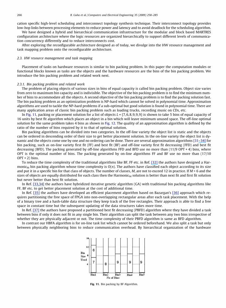
In Fig. 11, packing or placement solution for a list of objects L = {7,6,8,9,9,9} is shown to take 5 bins of equal capacity of16 units by best fit algorithm which places an object in a bin which will leave minimum unused space. The off-line optimalsolution for the same problem takes 4 bins as shown in Fig. 12. The quality of an approximation algorithm is defined by theratio of the number of bins required by it to that of optimal solution.
Bin packing algorithms can be divided into two categories. In the off-line variety the object list is static and the objectscan be ordered in descending order of their size to get better placement solution. In the on-line variety the object list is dy-namic and the objects come one by one and no ordering can be done. There are several approximation algorithms [31–34] forbin packing, such as on-line variety first fit (FF) and best fit (BF) and off-line variety first fit decreasing (FFD) and best fitdecreasing (BFD). The packing generated by off-line algorithms FFD and BFD use no more than (11/9 OPT + 4) bins, whereOPT is the optimal number of bins. The packing generated by on-line algorithms FF and BF use no more than (17/10OPT + 2) bins.
To reduce the time complexity of the traditional algorithms like BF, FF etc. in Ref. [32] the authors have designed a Har-monicM bin packing algorithm whose time complexity is O(n). The authors have classified each object according to its sizeand put it in a specific bin for that class of objects. The number of classes, M, are not to exceed 12 in practice. If M > 6 and thesizes of objects are equally distributed for each class then the HarmonicM solution is better than next fit and first fit solutionbut never better than best fit solution.
In Ref. [33,34] the authors have hybridized iterative genetic algorithm (GA) with traditional bin packing algorithms likeFF, BF etc. to get better placement solution at the cost of additional time.
In Ref. [35] the authors have developed an efficient placement algorithm based on Bazargan’s [36] approach which re-quires partitioning the free space of FPGA into non-overlapping rectangular areas after each task placement. With the helpof a binary tree and a hash-table data structure they keep track of the free rectangles. Their approach is able to find a freespace in constant time but the subsequent updating of the data structures takes more time.
In Ref. [37] the authors have proposed a partitioned best fit decreasing (PBFD) algorithm where they have divided a taskbetween bins if only it does not fit in any single bin. Their algorithm can split the task between any two bins irrespective ofwhether they are physically adjacent or not. The time complexity of their PBFD algorithm is same as BFD algorithm.
In contrast our HBFA algorithm is for on-line task list which cannot be ordered beforehand. We also split a task but onlybetween physically neighboring bins to reduce communication overhead. By hierarchical organization of the hardware
Fig. 11. Bin packing by BF Algorithm.
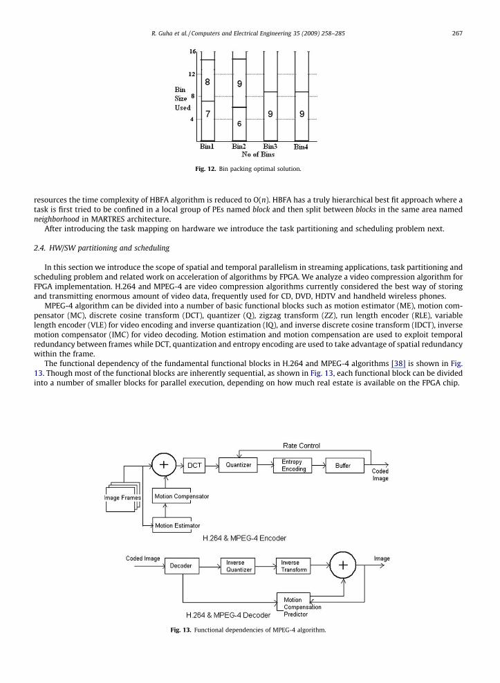
Fig. 12. Bin packing optimal solution.
R. Guha et al. / Computers and Electrical Engineering 35 (2009) 258–285 267
resources the time complexity of HBFA algorithm is reduced to O(n). HBFA has a truly hierarchical best fit approach where atask is first tried to be confined in a local group of PEs named block and then split between blocks in the same area namedneighborhood in MARTRES architecture.
After introducing the task mapping on hardware we introduce the task partitioning and scheduling problem next.
2.4. HW/SW partitioning and scheduling
In this section we introduce the scope of spatial and temporal parallelism in streaming applications, task partitioning andscheduling problem and related work on acceleration of algorithms by FPGA. We analyze a video compression algorithm forFPGA implementation. H.264 and MPEG-4 are video compression algorithms currently considered the best way of storingand transmitting enormous amount of video data, frequently used for CD, DVD, HDTV and handheld wireless phones.
MPEG-4 algorithm can be divided into a number of basic functional blocks such as motion estimator (ME), motion com-pensator (MC), discrete cosine transform (DCT), quantizer (Q), zigzag transform (ZZ), run length encoder (RLE), variablelength encoder (VLE) for video encoding and inverse quantization (IQ), and inverse discrete cosine transform (IDCT), inversemotion compensator (IMC) for video decoding. Motion estimation and motion compensation are used to exploit temporalredundancy between frames while DCT, quantization and entropy encoding are used to take advantage of spatial redundancywithin the frame.
The functional dependency of the fundamental functional blocks in H.264 and MPEG-4 algorithms [38] is shown in Fig.13. Though most of the functional blocks are inherently sequential, as shown in Fig. 13, each functional block can be dividedinto a number of smaller blocks for parallel execution, depending on how much real estate is available on the FPGA chip.
Fig. 13. Functional dependencies of MPEG-4 algorithm.
268 R. Guha et al. / Computers and Electrical Engineering 35 (2009) 258–285
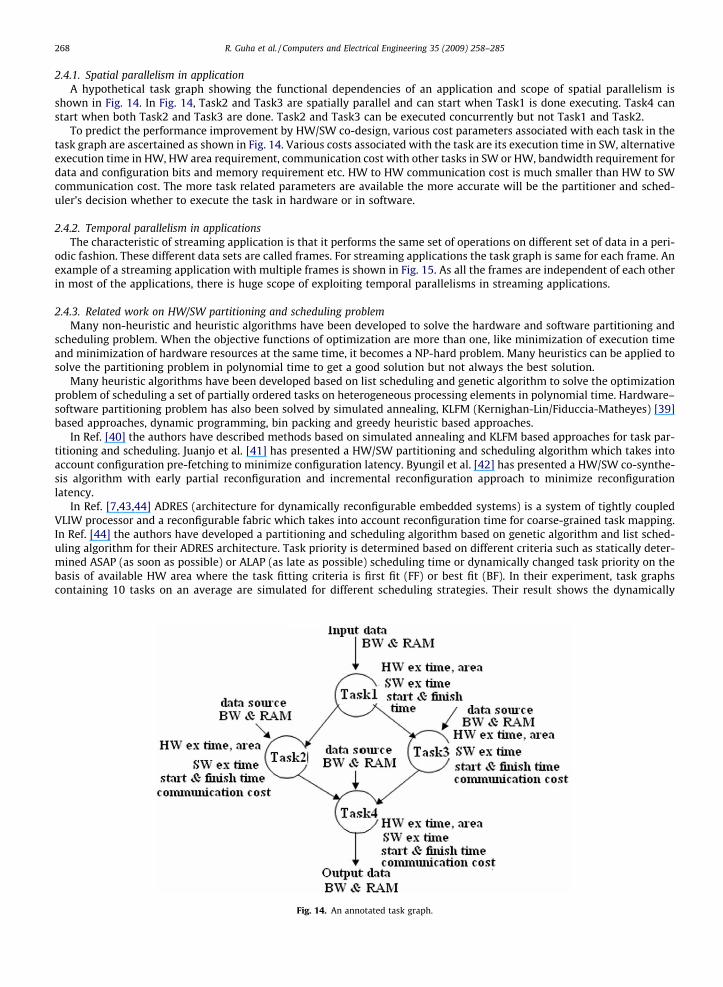
2.4.1. Spatial parallelism in applicationA hypothetical task graph showing the functional dependencies of an application and scope of spatial parallelism is
shown in Fig. 14. In Fig. 14, Task2 and Task3 are spatially parallel and can start when Task1 is done executing. Task4 canstart when both Task2 and Task3 are done. Task2 and Task3 can be executed concurrently but not Task1 and Task2.
To predict the performance improvement by HW/SW co-design, various cost parameters associated with each task in thetask graph are ascertained as shown in Fig. 14. Various costs associated with the task are its execution time in SW, alternativeexecution time in HW, HW area requirement, communication cost with other tasks in SW or HW, bandwidth requirement fordata and configuration bits and memory requirement etc. HW to HW communication cost is much smaller than HW to SWcommunication cost. The more task related parameters are available the more accurate will be the partitioner and sched-uler’s decision whether to execute the task in hardware or in software.
2.4.2. Temporal parallelism in applicationsThe characteristic of streaming application is that it performs the same set of operations on different set of data in a peri-
odic fashion. These different data sets are called frames. For streaming applications the task graph is same for each frame. Anexample of a streaming application with multiple frames is shown in Fig. 15. As all the frames are independent of each otherin most of the applications, there is huge scope of exploiting temporal parallelisms in streaming applications.
2.4.3. Related work on HW/SW partitioning and scheduling problemMany non-heuristic and heuristic algorithms have been developed to solve the hardware and software partitioning and
scheduling problem. When the objective functions of optimization are more than one, like minimization of execution timeand minimization of hardware resources at the same time, it becomes a NP-hard problem. Many heuristics can be applied tosolve the partitioning problem in polynomial time to get a good solution but not always the best solution.
Many heuristic algorithms have been developed based on list scheduling and genetic algorithm to solve the optimizationproblem of scheduling a set of partially ordered tasks on heterogeneous processing elements in polynomial time. Hardware–software partitioning problem has also been solved by simulated annealing, KLFM (Kernighan-Lin/Fiduccia-Matheyes) [39]based approaches, dynamic programming, bin packing and greedy heuristic based approaches.
In Ref. [40] the authors have described methods based on simulated annealing and KLFM based approaches for task par-titioning and scheduling. Juanjo et al. [41] has presented a HW/SW partitioning and scheduling algorithm which takes intoaccount configuration pre-fetching to minimize configuration latency. Byungil et al. [42] has presented a HW/SW co-synthe-sis algorithm with early partial reconfiguration and incremental reconfiguration approach to minimize reconfigurationlatency.
In Ref. [7,43,44] ADRES (architecture for dynamically reconfigurable embedded systems) is a system of tightly coupledVLIW processor and a reconfigurable fabric which takes into account reconfiguration time for coarse-grained task mapping.In Ref. [44] the authors have developed a partitioning and scheduling algorithm based on genetic algorithm and list sched-uling algorithm for their ADRES architecture. Task priority is determined based on different criteria such as statically deter-mined ASAP (as soon as possible) or ALAP (as late as possible) scheduling time or dynamically changed task priority on thebasis of available HW area where the task fitting criteria is first fit (FF) or best fit (BF). In their experiment, task graphscontaining 10 tasks on an average are simulated for different scheduling strategies. Their result shows the dynamically
Fig. 14. An annotated task graph.
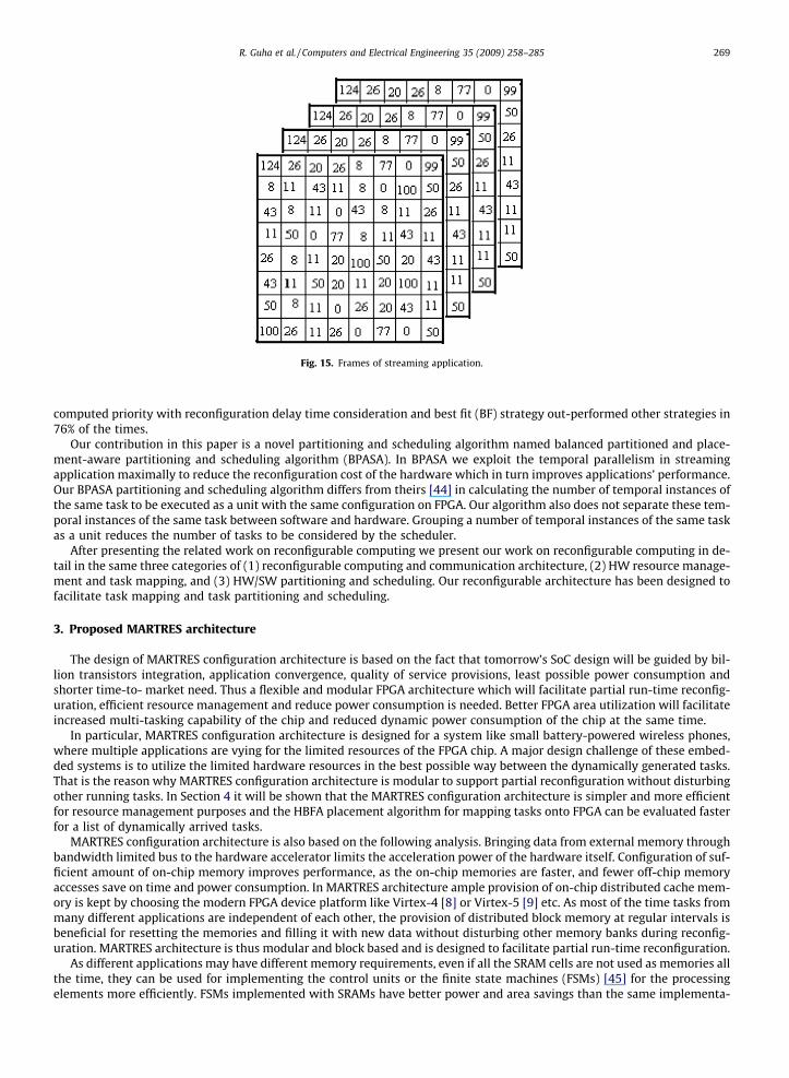
Fig. 15. Frames of streaming application.
R. Guha et al. / Computers and Electrical Engineering 35 (2009) 258–285 269
computed priority with reconfiguration delay time consideration and best fit (BF) strategy out-performed other strategies in76% of the times.
Our contribution in this paper is a novel partitioning and scheduling algorithm named balanced partitioned and place-ment-aware partitioning and scheduling algorithm (BPASA). In BPASA we exploit the temporal parallelism in streamingapplication maximally to reduce the reconfiguration cost of the hardware which in turn improves applications’ performance.Our BPASA partitioning and scheduling algorithm differs from theirs [44] in calculating the number of temporal instances ofthe same task to be executed as a unit with the same configuration on FPGA. Our algorithm also does not separate these tem-poral instances of the same task between software and hardware. Grouping a number of temporal instances of the same taskas a unit reduces the number of tasks to be considered by the scheduler.
After presenting the related work on reconfigurable computing we present our work on reconfigurable computing in de-tail in the same three categories of (1) reconfigurable computing and communication architecture, (2) HW resource manage-ment and task mapping, and (3) HW/SW partitioning and scheduling. Our reconfigurable architecture has been designed tofacilitate task mapping and task partitioning and scheduling.
3. Proposed MARTRES architecture
The design of MARTRES configuration architecture is based on the fact that tomorrow’s SoC design will be guided by bil-lion transistors integration, application convergence, quality of service provisions, least possible power consumption andshorter time-to- market need. Thus a flexible and modular FPGA architecture which will facilitate partial run-time reconfig-uration, efficient resource management and reduce power consumption is needed. Better FPGA area utilization will facilitateincreased multi-tasking capability of the chip and reduced dynamic power consumption of the chip at the same time.
In particular, MARTRES configuration architecture is designed for a system like small battery-powered wireless phones,where multiple applications are vying for the limited resources of the FPGA chip. A major design challenge of these embed-ded systems is to utilize the limited hardware resources in the best possible way between the dynamically generated tasks.That is the reason why MARTRES configuration architecture is modular to support partial reconfiguration without disturbingother running tasks. In Section 4 it will be shown that the MARTRES configuration architecture is simpler and more efficientfor resource management purposes and the HBFA placement algorithm for mapping tasks onto FPGA can be evaluated fasterfor a list of dynamically arrived tasks.
MARTRES configuration architecture is also based on the following analysis. Bringing data from external memory throughbandwidth limited bus to the hardware accelerator limits the acceleration power of the hardware itself. Configuration of suf-ficient amount of on-chip memory improves performance, as the on-chip memories are faster, and fewer off-chip memoryaccesses save on time and power consumption. In MARTRES architecture ample provision of on-chip distributed cache mem-ory is kept by choosing the modern FPGA device platform like Virtex-4 [8] or Virtex-5 [9] etc. As most of the time tasks frommany different applications are independent of each other, the provision of distributed block memory at regular intervals isbeneficial for resetting the memories and filling it with new data without disturbing other memory banks during reconfig-uration. MARTRES architecture is thus modular and block based and is designed to facilitate partial run-time reconfiguration.
As different applications may have different memory requirements, even if all the SRAM cells are not used as memories allthe time, they can be used for implementing the control units or the finite state machines (FSMs) [45] for the processingelements more efficiently. FSMs implemented with SRAMs have better power and area savings than the same implementa-
270 R. Guha et al. / Computers and Electrical Engineering 35 (2009) 258–285
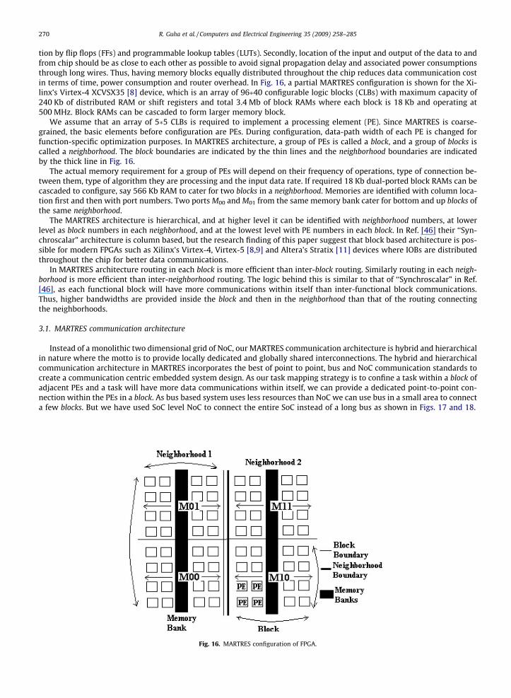
tion by flip flops (FFs) and programmable lookup tables (LUTs). Secondly, location of the input and output of the data to andfrom chip should be as close to each other as possible to avoid signal propagation delay and associated power consumptionsthrough long wires. Thus, having memory blocks equally distributed throughout the chip reduces data communication costin terms of time, power consumption and router overhead. In Fig. 16, a partial MARTRES configuration is shown for the Xi-linx’s Virtex-4 XCVSX35 [8] device, which is an array of 96�40 configurable logic blocks (CLBs) with maximum capacity of240 Kb of distributed RAM or shift registers and total 3.4 Mb of block RAMs where each block is 18 Kb and operating at500 MHz. Block RAMs can be cascaded to form larger memory block.
We assume that an array of 5�5 CLBs is required to implement a processing element (PE). Since MARTRES is coarse-grained, the basic elements before configuration are PEs. During configuration, data-path width of each PE is changed forfunction-specific optimization purposes. In MARTRES architecture, a group of PEs is called a block, and a group of blocks iscalled a neighborhood. The block boundaries are indicated by the thin lines and the neighborhood boundaries are indicatedby the thick line in Fig. 16.
The actual memory requirement for a group of PEs will depend on their frequency of operations, type of connection be-tween them, type of algorithm they are processing and the input data rate. If required 18 Kb dual-ported block RAMs can becascaded to configure, say 566 Kb RAM to cater for two blocks in a neighborhood. Memories are identified with column loca-tion first and then with port numbers. Two ports M00 and M01 from the same memory bank cater for bottom and up blocks ofthe same neighborhood.
The MARTRES architecture is hierarchical, and at higher level it can be identified with neighborhood numbers, at lowerlevel as block numbers in each neighborhood, and at the lowest level with PE numbers in each block. In Ref. [46] their ‘‘Syn-chroscalar” architecture is column based, but the research finding of this paper suggest that block based architecture is pos-sible for modern FPGAs such as Xilinx’s Virtex-4, Virtex-5 [8,9] and Altera’s Stratix [11] devices where IOBs are distributedthroughout the chip for better data communications.
In MARTRES architecture routing in each block is more efficient than inter-block routing. Similarly routing in each neigh-borhood is more efficient than inter-neighborhood routing. The logic behind this is similar to that of ‘‘Synchroscalar” in Ref.[46], as each functional block will have more communications within itself than inter-functional block communications.Thus, higher bandwidths are provided inside the block and then in the neighborhood than that of the routing connectingthe neighborhoods.
3.1. MARTRES communication architecture
Instead of a monolithic two dimensional grid of NoC, our MARTRES communication architecture is hybrid and hierarchicalin nature where the motto is to provide locally dedicated and globally shared interconnections. The hybrid and hierarchicalcommunication architecture in MARTRES incorporates the best of point to point, bus and NoC communication standards tocreate a communication centric embedded system design. As our task mapping strategy is to confine a task within a block ofadjacent PEs and a task will have more data communications within itself, we can provide a dedicated point-to-point con-nection within the PEs in a block. As bus based system uses less resources than NoC we can use bus in a small area to connecta few blocks. But we have used SoC level NoC to connect the entire SoC instead of a long bus as shown in Figs. 17 and 18.
Fig. 16. MARTRES configuration of FPGA.

R. Guha et al. / Computers and Electrical Engineering 35 (2009) 258–285 271
The shared connection in a neighborhood can be a bus system if the bus length is within the limit of clock-skew problem.Alternatively the shared connection in a neighborhood can be a two dimensional grid network and NoC based. In that casethere are two levels of NoC, one at neighborhood level and another at SoC or chip level. We have designed the hybrid andhierarchical communication network to save on communication resources without sacrificing on the speed of operationsof the processors.
It is obvious that bus system in a neighborhood will use less communication resources than NoC system in a neighborhood.Even if we use NoC system in a neighborhoodwe save on communication resources because of the hierarchical nature of theNoC in the chip. As for example if 81 IP blocks such as processing elements or memories were connected in one level of NoCof 9�9 two dimensional grids there would be 144 interconnects. Instead if we connect the 81 IP blocks in two levels of NoC asshown in Fig. 18 then there will be 9 clusters and in each cluster there will be 9 IP blocks. In each cluster the IP blocks areconnected by first level NoC of 3�3 two dimensional grids. The 9 clusters in the chip are connected by the second level NoC of3�3 two dimensional grids. In this hierarchical NoC there are 12 interconnects in each cluster, 12 interconnects in secondlevel NoC in the chip and thus total 12�9 + 12 = 120 interconnects in the entire SoC. As number of IP blocks, which is 81,is much less than total number of interconnects which is 120, communication concurrency is not much suffered in compar-ison to one level NoC with 144 interconnects for the entire chip. Within a cluster communication concurrency is maximumand is same as one level NoC.
Communication resources can also be saved by using bus system for a small group of IP blocks without sacrificing muchon operating speed and throughput as analyzed here. In our example the SoC is assumed to be implemented with 90 nmprocess technology. For 90 nm process technology the gate delay is 60 ps (pico seconds) and D Flip Flop (DFF) traversal timewhich includes setup and hold time is 0.3 ns (nano seconds) [27]. We assume it takes 3 gates or fewer stages for decisionlogic to latch the data to bus for up to 9 PEs connected to the same bus. We assume a clock skew of .3 ns when the busis 3 mm long. We assume the propagation delay of data for a properly buffered wire of length 2 mm is .44 ns and of length3 mm is .66 ns.
Thus transport time across 2 mm wire including the clock-skew and DFF traversal time takes .44 + 3� .06 + .3 + .3 =1.22 ns. So the maximum operating frequency of 2 mm wire is, f = 1/1.22 � 800 MHz.
Similarly, transport time across 3 mm wire including the clock-skew and DFF traversal time takes .66 + 3�.06 + .3 + .3 =1.44 ns. So the maximum operating frequency of 3 mm wire is, f = 1/1.44 � 690 MHz.
We now compare the two communication infrastructure named Option 1 and Option 2 as shown in Figs. 17 and 18, interms of operating frequency, throughput and resource usage by varying the number of neighborhoods (N) in the entire chip,
Fig. 17. Neighborhood level bus.
Fig. 18. Neighborhood level NoC.

272 R. Guha et al. / Computers and Electrical Engineering 35 (2009) 258–285
number of blocks (B) per neighborhood and number of PEs (P) in a block for a given number of PEs in a chip. Depending on theoperating frequency and throughput requirement of an application the best architecture which can save on communicationresource usage can be chosen.
Option 1The communication infrastructure of Option 1 as shown in Fig. 17 is as follows:
(a) PEs in a block are connected by point-to-point connection.(b) Blocks in a neighborhood are connected by bus.(c) Neighborhoods in a chip are connected by 2 D mesh NoC.
Total interconnect length, L in the whole chip in this case can be formulated as Eq. (1):
L ¼ B � N½ðP � 1Þ � f1þ ðP � 1Þg=2� þ ½Bus Length � N� þ ½Level2 interconnect �ffiffiffiffiNp� 1
� � ffiffiffiffiNp� 2�; ð1Þ
where Bus_Length = l, N is the number of neighborhoods in the entire chip, B is the number of blocks per neighborhood and P isthe number of PEs in a block. We assume bus length of 2 mm for connecting 4 PEs and bus length of 3 mm for connecting 9PEs. We assume interconnect length of 2 mm for connecting the neighborhoods in a NoC. The higher interconnect length be-tween the bus and second level NoC will determine the frequency of operation in a system. Thus with the similar calculationas above the operating frequency of 2 mm bus is 800 MHz and 3 mm bus is 690 MHz. The peak throughput, T, of the systemwill be determined by the number of bus and operating frequency, f, of the system and can be formulated as T = 4�N�f wherenumber of bus is equal to number of neighborhoods, N in MARTRES architecture. We assume 4 bytes wide data transfer.
Option 2The communication infrastructure of Option 2 as shown in Fig. 18 is as follows:
(a) PEs in a block are connected by point-to-point connection.(b) Blocks in a neighborhood are connected by 2D mesh NoC.(c) Neighborhoods in a chip are connected by 2 D mesh NoC.
Total interconnect length, L in the whole chip in this case can be formulated as Eq. (2):
L ¼ B � N½ðP � 1Þ � f1þ ðP � 1Þg=2� þ Level1 interconnect length � N �ffiffiffiBp� 1
� ��ffiffiffiBp� 2
h i
þ ½Level2 interconnect length �ffiffiffiffiNp� 1Þ �
ffiffiffiffiNp� 2
� ið2Þ
where l is the higher of the Level1_interconnect_length and Level2_interconnect_length, N is the number of neighborhoods inthe entire chip, B is the number of blocks per neighborhood and P is the number of PEs in a block as before.
The interconnect length in the first level NoC is assumed to be 1 mm whereas in second level NoC it is 2 mm. The higherinterconnect length between the first level NoC and second level NoC will determine the frequency of operation in a system.Thus with the similar calculation as above the operating frequency of 2 mm interconnect is 800 MHz. The peak throughput,T, of the system will be determined by the size of the NoC and operating frequency, f, of the system and can be formulated asT = 4�N�f where the NoC size is equal to number of neighborhood, N. We assume 4 bytes wide data transfer as before.
Table 2 compares two different options of connecting the PEs in different size chips and what frequency and throughputthey can support and what will be the corresponding interconnect cost. As seen from Table 2, Option 1 of connecting the PEsin a chip uses much less resources than Option 2 without sacrificing much of the system support of operating frequencies andthroughput for a small size bus. Communication resource savings also implies power savings of the chip. Thus bus can beused for a small number of PEs in a local area.
Next we show how MARTRES configuration architecture facilitates HW resource management and task mapping.
4. HW resource management
We have created MARTRES configuration architecture so that the HBFA placement algorithm takes less time for map-ping tasks. A hardware resource manager can keep track of all the resources in MARTRES architecture in a hierarchical fash-ion, first by a neighborhood number, then by a block number in a neighborhood and finally by a PE number in each block.Suppose MARTRES has 8�8 array of PEs. First the PEs are grouped together as blocks and then as neighborhoods. Supposeeach block has 4�4 PE array and each neighborhood has 2�1 block array or 8�4 PE array. So the whole chip consists of 2neighborhoods, 4 blocks and 64 individual PEs. Each block is identified by its participation in which neighborhood firstand then by its number. So the blocks are identified as blocki,j where i = 1 to N, N being the number of neighborhoodsand j = 1 to B, B being the number of blocks in each neighborhood. Each PE is identified by its participation in which neigh-borhood first and then in which block and then by its number. So the PEs are identified as PEi,j,k where i = 1 to N, N being thenumber of neighborhoods, j = 1 to B, B being the number of blocks in each neighborhood and k = 1 to P, P being the number ofPEs in each block.
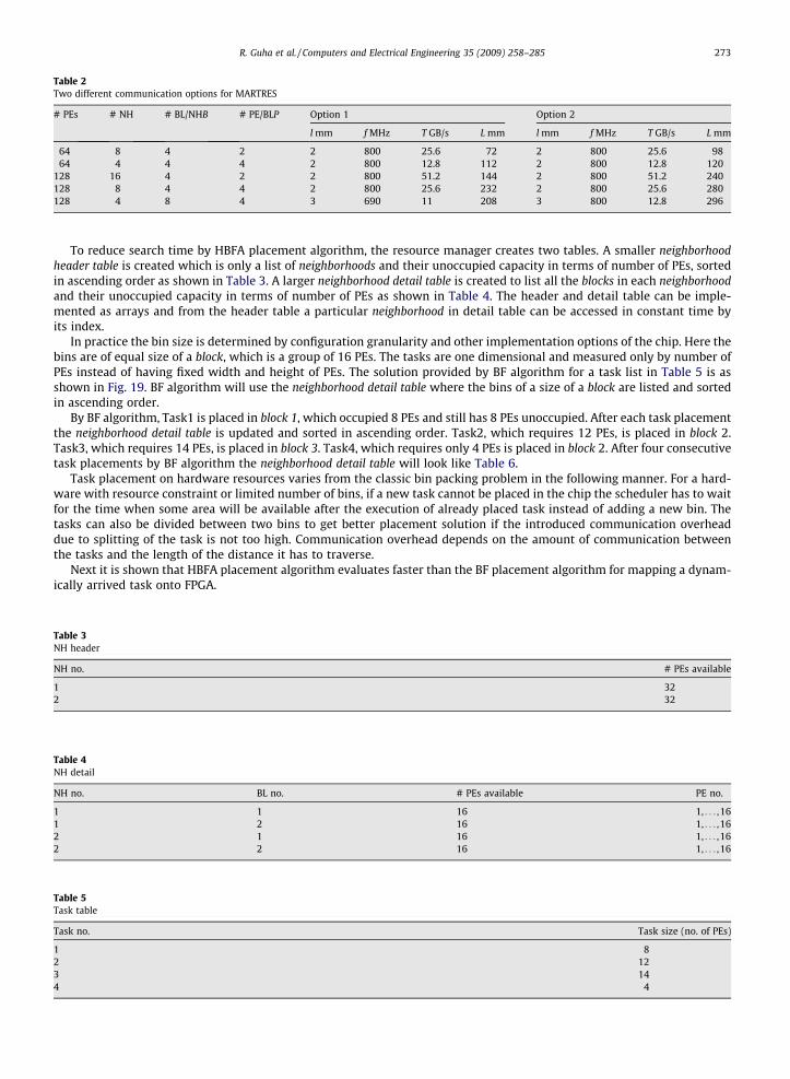
Table 2Two different communication options for MARTRES
# PEs # NH # BL/NHB # PE/BLP Option 1 Option 2
l mm f MHz T GB/s L mm l mm f MHz T GB/s L mm
64 8 4 2 2 800 25.6 72 2 800 25.6 9864 4 4 4 2 800 12.8 112 2 800 12.8 120
128 16 4 2 2 800 51.2 144 2 800 51.2 240128 8 4 4 2 800 25.6 232 2 800 25.6 280128 4 8 4 3 690 11 208 3 800 12.8 296
R. Guha et al. / Computers and Electrical Engineering 35 (2009) 258–285 273
To reduce search time by HBFA placement algorithm, the resource manager creates two tables. A smaller neighborhoodheader table is created which is only a list of neighborhoods and their unoccupied capacity in terms of number of PEs, sortedin ascending order as shown in Table 3. A larger neighborhood detail table is created to list all the blocks in each neighborhoodand their unoccupied capacity in terms of number of PEs as shown in Table 4. The header and detail table can be imple-mented as arrays and from the header table a particular neighborhood in detail table can be accessed in constant time byits index.
In practice the bin size is determined by configuration granularity and other implementation options of the chip. Here thebins are of equal size of a block, which is a group of 16 PEs. The tasks are one dimensional and measured only by number ofPEs instead of having fixed width and height of PEs. The solution provided by BF algorithm for a task list in Table 5 is asshown in Fig. 19. BF algorithm will use the neighborhood detail table where the bins of a size of a block are listed and sortedin ascending order.
By BF algorithm, Task1 is placed in block 1, which occupied 8 PEs and still has 8 PEs unoccupied. After each task placementthe neighborhood detail table is updated and sorted in ascending order. Task2, which requires 12 PEs, is placed in block 2.Task3, which requires 14 PEs, is placed in block 3. Task4, which requires only 4 PEs is placed in block 2. After four consecutivetask placements by BF algorithm the neighborhood detail table will look like Table 6.
Task placement on hardware resources varies from the classic bin packing problem in the following manner. For a hard-ware with resource constraint or limited number of bins, if a new task cannot be placed in the chip the scheduler has to waitfor the time when some area will be available after the execution of already placed task instead of adding a new bin. Thetasks can also be divided between two bins to get better placement solution if the introduced communication overheaddue to splitting of the task is not too high. Communication overhead depends on the amount of communication betweenthe tasks and the length of the distance it has to traverse.
Next it is shown that HBFA placement algorithm evaluates faster than the BF placement algorithm for mapping a dynam-ically arrived task onto FPGA.
Table 3NH header
NH no. # PEs available
1 322 32
Table 4NH detail
NH no. BL no. # PEs available PE no.
1 1 16 1, . . . ,161 2 16 1, . . . ,162 1 16 1, . . . ,162 2 16 1, . . . ,16
Table 5Task table
Task no. Task size (no. of PEs)
1 82 123 144 4

Fig. 19. Four consecutive tasks placement by BF.
Table 6NH detail after 4 tasks placement by BF
NH no. BL no. # PEs available PE no.
1 2 02 3 2 15,161 1 8 9, . . . ,162 4 16 1,2, . . . ,16
274 R. Guha et al. / Computers and Electrical Engineering 35 (2009) 258–285
4.1. Proposed placement algorithm, HBFA
HBFA algorithm is based on the following analysis. For the bin packing problem we argue that, if the bin capacity is com-paratively larger than individual object sizes then the total number of bins, OPT, required for optimal solution is smaller thanthe solution obtained when the object sizes are larger. This is because more objects can be packed in the same bin and thereis less chances of larger unoccupied wasted space in each bin. If OPT is small then approximate solution of BF algorithmwhich is less than or equal to (17/10OPT + 2) is also small. Thus difference between an optimal solution and an approximatesolution varies depending on average relative size of bin capacity and object sizes. Analytically either the object size shouldbe equal to the bin size or between 0% and 30% of the bin size so that there will be less % of each bin remaining unutilizedafter placement of several objects.
To prove the above analysis, Fig. 20 maps a task list with relatively smaller size tasks such as L = {2,4,4,3,2,4,2,2,4,3,3,2,1,4,4,4} with BF algorithm and compares it with the optimal solution. Total task size in that list is 48 and optimalsolution took 3 bins and approximate solution took 4 bins of size 16 units each. Figs. 11 and 12 in Section 2, mapped atask list with relatively larger size tasks such as L = {6,7,8,9,9,9} also totaling to 48 with BF algorithm and compared itwith the optimal solution before. In that case optimal solution took 4 bins and approximate solution took even largernumber of 5 bins. So to increase the bin size in HBFA algorithm, we group a number of smaller bins to make a largerbin. In the lower level the bin size is smaller and is labeled as a block (BL). In the higher level the bin size is largerand is labeled as neighborhood (NH) which is a group of blocks. Both NH and BL bin sizes are measured in number ofPEs.
HBFA algorithm is a novel variety of bin packing algorithm designed for MARTRES architecture. The algorithm is so calledbecause the resources or bins are listed hierarchically and searched hierarchically and only the higher level bins are sorted inascending order. The placement algorithm first searches the higher level bins listed in the smaller neigborhood header table toensure available capacity in a neighborhood is enough for a task and then goes to the lower level bins listed in larger neig-borhood detail table for determining exact physical location for that task in that neighborhood.
4.1.1. Allowing different task sizes by HBFAIf we can control the task size we make the task size much smaller than the neighborhood size to make our approximate
solution close to optimal solution. For mapping a task, if the task size is smaller than a neighborhood size the neighborhoodheader table will be searched in forward order starting from the top of the list. In the first try no task will be split betweentwo neighborhoods to avoid inter-neighborhood communication delay. But if a task cannot be placed in any neighborhood thenit can be split between neighborhoods. If task related parameters like communication cost of tasks are available and two taskshave many communications between them then their combined size can be considered so that they both can be placed in thesame neighborhood to reduce communication cost.
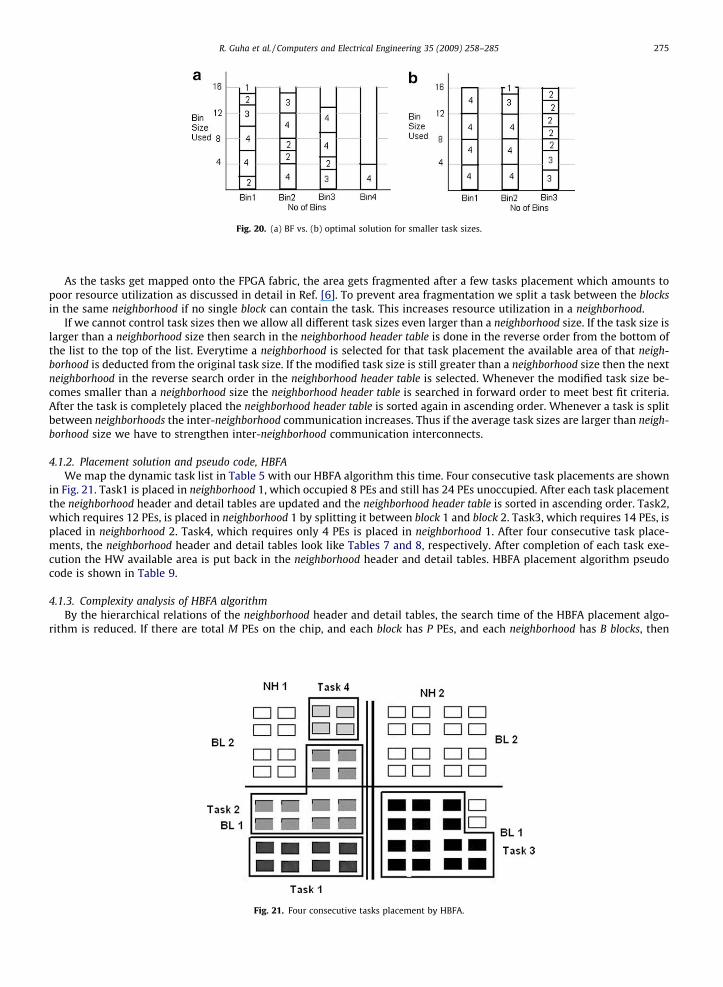
Fig. 20. (a) BF vs. (b) optimal solution for smaller task sizes.
R. Guha et al. / Computers and Electrical Engineering 35 (2009) 258–285 275
As the tasks get mapped onto the FPGA fabric, the area gets fragmented after a few tasks placement which amounts topoor resource utilization as discussed in detail in Ref. [6]. To prevent area fragmentation we split a task between the blocksin the same neighborhood if no single block can contain the task. This increases resource utilization in a neighborhood.
If we cannot control task sizes then we allow all different task sizes even larger than a neighborhood size. If the task size islarger than a neighborhood size then search in the neighborhood header table is done in the reverse order from the bottom ofthe list to the top of the list. Everytime a neighborhood is selected for that task placement the available area of that neigh-borhood is deducted from the original task size. If the modified task size is still greater than a neighborhood size then the nextneighborhood in the reverse search order in the neighborhood header table is selected. Whenever the modified task size be-comes smaller than a neighborhood size the neighborhood header table is searched in forward order to meet best fit criteria.After the task is completely placed the neighborhood header table is sorted again in ascending order. Whenever a task is splitbetween neighborhoods the inter-neighborhood communication increases. Thus if the average task sizes are larger than neigh-borhood size we have to strengthen inter-neighborhood communication interconnects.
4.1.2. Placement solution and pseudo code, HBFAWe map the dynamic task list in Table 5 with our HBFA algorithm this time. Four consecutive task placements are shown
in Fig. 21. Task1 is placed in neighborhood 1, which occupied 8 PEs and still has 24 PEs unoccupied. After each task placementthe neighborhood header and detail tables are updated and the neighborhood header table is sorted in ascending order. Task2,which requires 12 PEs, is placed in neighborhood 1 by splitting it between block 1 and block 2. Task3, which requires 14 PEs, isplaced in neighborhood 2. Task4, which requires only 4 PEs is placed in neighborhood 1. After four consecutive task place-ments, the neighborhood header and detail tables look like Tables 7 and 8, respectively. After completion of each task exe-cution the HW available area is put back in the neighborhood header and detail tables. HBFA placement algorithm pseudocode is shown in Table 9.
4.1.3. Complexity analysis of HBFA algorithmBy the hierarchical relations of the neighborhood header and detail tables, the search time of the HBFA placement algo-
rithm is reduced. If there are total M PEs on the chip, and each block has P PEs, and each neighborhood has B blocks, then
Fig. 21. Four consecutive tasks placement by HBFA.

276 R. Guha et al. / Computers and Electrical Engineering 35 (2009) 258–285
we have a total of N neighborhoods, where N = M/(B�P) and here the neighborhood or bin size is (B�P). So, in the first level, thenumber of bins to search is N = M/(B�P). In the second level of search, the block or bin size is P and the number of blocks orbins to search is B. So, in the worst case total search time is (M/(B�P)) + B for each task placement. Whereas in one level of BFplacement algorithm where the bin size is P or a block, the number of bins to search is M/P. After each placement the bin listis sorted in ascending order to meet best fit criteria, and in the worst case sorting takes O(n2) time, where n is the number ofitems in the list. In our hierarchical HBFA algorithm only the neighborhood header table is sorted and it takes O((M/(B�P))2)time. In one level BF algorithm the sorting time is O((M/P)2). From the above example we can formulate the complexity ofHBFA algorithm and can compare it with that of BF algorithm.
Table 7NH header after 4 tasks placement by HBFA
NH no. # PEs available
1 82 18
Table 9HBFA algorithm pseudo code
Create array Task_List[Task1, . . .Taskm]//m number of tasksCreate array NH_Header[NH1,. . .NHN]//sorted in ascending order of available capacity, N number of neighborhoodsCreate array NH_Detail[NH1, . . .NHN][ BL1,. . .BLB]//B, Number of blocks configured in each neighborhoodCreate variable max_NH//max neighborhood sizeHBFA(Task_list, NH_Header, NH_Detail)for i 1 to length[Task_list]if Task_list [i]< = max_NH then//forward search
Forward_Search:for j 1 to length[NH_header]
if (Task_list [i]< = NH_header[j])//task is placed in jth neighborhoodthen NH_header[j] = NH_header[j] � Task_list [i]
SORT (NH_header)//ascending order for Best FitTASK_PLACEMENT(Task_List[i], NH_Detail[j][])
else//reverse searchmodified_task_size = Task_list [i]Reverse_Search:for j length[NH_header] to 1
if modified_task_size> max_NH thenTASK_PLACEMENT(NH_header[j], NH_detail[j][])modified_task_size- = NH_header[j]
NH_header[j] = 0else Task_list [i] = modified_task_size
go to Forward_SearchTASK_PLACEMENT(Task_list[i], NH_detail[j][])//task can be split between blocksfor k 1 to B//B, Number of blocks configured in each neighborhood
if Task_list[i] > NH_detail[j][k]thenTask_list[i] = Task_list[i] � NH_detail[j][k]NH_detail[j][k] = 0;
Else NH_detail[j][k] = NH_detail[j][k] � Task_list[i]
Table 8NH detail after 4 tasks placement by HBFA
NH no. BL no. #PEs available PE no.
1 1 01 2 8 9, . . . ,162 1 2 15,162 2 16 1, . . . ,16
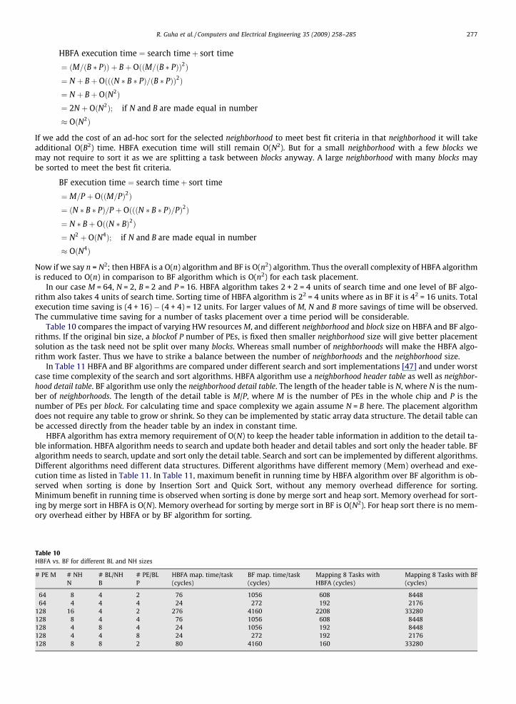
Table 1HBFA v
# PE M
6464
128128128128128
R. Guha et al. / Computers and Electrical Engineering 35 (2009) 258–285 277
HBFA execution time ¼ search timeþ sort time
¼ ðM=ðB � PÞÞ þ Bþ OððM=ðB � PÞÞ2Þ¼ N þ Bþ OðððN � B � PÞ=ðB � PÞÞ2Þ¼ N þ Bþ OðN2Þ¼ 2N þ OðN2Þ; if N and B are made equal in number
� OðN2Þ
If we add the cost of an ad-hoc sort for the selected neighborhood to meet best fit criteria in that neighborhood it will takeadditional O(B2) time. HBFA execution time will still remain O(N2). But for a small neighborhood with a few blocks wemay not require to sort it as we are splitting a task between blocks anyway. A large neighborhood with many blocks maybe sorted to meet the best fit criteria.
BF execution time ¼ search timeþ sort time
¼ M=P þ OððM=PÞ2Þ¼ ðN � B � PÞ=P þ OðððN � B � PÞ=PÞ2Þ¼ N � Bþ OððN � BÞ2Þ¼ N2 þ OðN4Þ; if N and B are made equal in number
� OðN4Þ
Now if we say n = N2; then HBFA is a O(n) algorithm and BF is O(n2) algorithm. Thus the overall complexity of HBFA algorithmis reduced to O(n) in comparison to BF algorithm which is O(n2) for each task placement.
In our case M = 64, N = 2, B = 2 and P = 16. HBFA algorithm takes 2 + 2 = 4 units of search time and one level of BF algo-rithm also takes 4 units of search time. Sorting time of HBFA algorithm is 22 = 4 units where as in BF it is 42 = 16 units. Totalexecution time saving is (4 + 16) � (4 + 4) = 12 units. For larger values of M, N and B more savings of time will be observed.The cummulative time saving for a number of tasks placement over a time period will be considerable.
Table 10 compares the impact of varying HW resources M, and different neighborhood and block size on HBFA and BF algo-rithms. If the original bin size, a blockof P number of PEs, is fixed then smaller neighborhood size will give better placementsolution as the task need not be split over many blocks. Whereas small number of neighborhoods will make the HBFA algo-rithm work faster. Thus we have to strike a balance between the number of neighborhoods and the neighborhood size.
In Table 11 HBFA and BF algorithms are compared under different search and sort implementations [47] and under worstcase time complexity of the search and sort algorithms. HBFA algorithm use a neighborhood header table as well as neighbor-hood detail table. BF algorithm use only the neighborhood detail table. The length of the header table is N, where N is the num-ber of neighborhoods. The length of the detail table is M/P, where M is the number of PEs in the whole chip and P is thenumber of PEs per block. For calculating time and space complexity we again assume N = B here. The placement algorithmdoes not require any table to grow or shrink. So they can be implemented by static array data structure. The detail table canbe accessed directly from the header table by an index in constant time.
HBFA algorithm has extra memory requirement of O(N) to keep the header table information in addition to the detail ta-ble information. HBFA algorithm needs to search and update both header and detail tables and sort only the header table. BFalgorithm needs to search, update and sort only the detail table. Search and sort can be implemented by different algorithms.Different algorithms need different data structures. Different algorithms have different memory (Mem) overhead and exe-cution time as listed in Table 11. In Table 11, maximum benefit in running time by HBFA algorithm over BF algorithm is ob-served when sorting is done by Insertion Sort and Quick Sort, without any memory overhead difference for sorting.Minimum benefit in running time is observed when sorting is done by merge sort and heap sort. Memory overhead for sort-ing by merge sort in HBFA is O(N). Memory overhead for sorting by merge sort in BF is O(N2). For heap sort there is no mem-ory overhead either by HBFA or by BF algorithm for sorting.
0s. BF for different BL and NH sizes
# NHN
# BL/NHB
# PE/BLP
HBFA map. time/task(cycles)
BF map. time/task(cycles)
Mapping 8 Tasks withHBFA (cycles)
Mapping 8 Tasks with BF(cycles)
8 4 2 76 1056 608 84484 4 4 24 272 192 2176
16 4 2 276 4160 2208 332808 4 4 76 1056 608 84484 8 4 24 1056 192 84484 4 8 24 272 192 21768 8 2 80 4160 160 33280
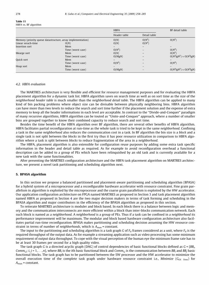
Table 11HBFA vs. BF algorithm
HBFA BF detail table
Header table Detail table
Memory (priority queue datastructure, array implementation) O(N) O(N2) O(N2)Linear serach-time O(N) O(N) O(N2)Insertion sort Mem – – –
Time (worst case) O(N2) – O(N4)Mearge sort Mem O(N) – O(N2)
Time (worst case) O(NlgN) – O(N2lgN2) � O(N2lgN)Quick sort Mem – – –
Time (worst case) O(N2) – O(N4)Heap sort Mem – – –
Time (worst case) O(NlgN) – O(N2lgN2) � O(N2lgN)
278 R. Guha et al. / Computers and Electrical Engineering 35 (2009) 258–285
4.2. HBFA evaluation
The MARTRES architecture is very flexible and efficient for resource management purposes and for evaluating the HBFAplacement algorithm for a dynamic task list. HBFA algorithm saves on search time as well as on sort time as the size of theneighborhood header table is much smaller than the neighborhood detail table. The HBFA algorithm can be applied to manykind of bin packing problems where object size can be divisable between physically neighboring bins. HBFA algorithmcan have more than two levels to reduce the search and sort time further if the placement solution and the expense of extramemory to keep all the header informations in each level are acceptable. In contrast to the ‘‘Divide-and-Conquer” paradigmof many recursive algorithms, HBFA algorithm can be touted as ‘‘Unite-and-Conquer” approach, where a number of smallerbins are grouped together to know their combined capacity to reduce search and sort time.
Besides the time benefit of the HBFA algorithm over BF algorithm, there are several other benefits of HBFA algorithm.HBFA facilitates partial reconfiguration at run-time as the whole task is tried to be kept in the same neighborhood. Confininga task in the same neighborhood also reduces the communication cost in a task. In BF algorithm the bin size is a block and asingle task is not split between the blocks in the first try thus it has poor resource utilization in comparison to HBFA algo-rithm where a task is split between blocks to reduce fragmentation of the area in a neighborhood.
The HBFA, placement algorithm is also extensible for configuration reuse purposes by adding some extra task specificinformation in the header and detail table as required. As for example to avoid reconfiguration overhead a functionaldescription can be added to a group of PEs which have been relinquished by an old task and is currently available for anew task with the same functionalities.
After presenting the MARTRES configuration architecture and the HBFA task placement algorithm on MARTRES architec-ture, we present a novel task partitioning and scheduling algorithm next.
5. BPASA algorithm
In this section we propose a balanced partitioned and placement-aware partitioning and scheduling algorithm (BPASA)for a hybrid system of a microprocessor and a reconfigurable hardware accelerator with resource constraint. Fine grain par-allelism in algorithm is exploited by the microprocessor and the coarse grain parallelism is exploited by the HW accelerator.Our application configuration architecture on FPGA named MARTRES as proposed in Section 3 and task placement algorithmnamed HBFA as proposed in Section 4 are the two major decision makers in terms of task forming and scheduling in theBPASA algorithm and major contributors in the efficiency of the BPASA algorithm as proposed in this section.
To reiterate MARTRES architecture is moduler and block based. In each block there is a balance between logic and mem-ory and the communication interconnects are more efficient within a block than inter-blocks communication network. Eachsuch block is named as a neighborhood. A neighborhood is a group of PEs. Thus if a task can be confined in a neighborhood itsperformance improvement will be maximum. The modular and block based hardware configuration architecture also facil-itates partial run-time reconfiguration. BPASA makes partitioning and scheduling decision assuming the HW resource con-straint in terms of number of neighborhoods, which is Amax = constant.
The input to the partitioning and scheduling algorithm is a task graph G of Fd frames considered as a unit, where Fd is therequired throughput of the output data. As for example a streaming application such as video processing has some minimumrequirement of output data throughput. To cope with the visual perception of the human eye the minimum frame rate has tobe at least 30 frames per second for a high quality video.
The task graph G is a directed acyclic graph (DAG) of control dependencies of basic functional blocks defined as G = {BBi,Commi,j; i, j = 1, . . . ,n}, where BBi is the ith basic functional block and Commi,j is the communication between BBi and BBj basicfunctional blocks. The task graph has to be partitioned between the SW processor and the HW accelerator to minimize theoverall execution time of the complete task graph under hardware resource constraint i.e., Minimize (GEX Time) forAmax = constant.
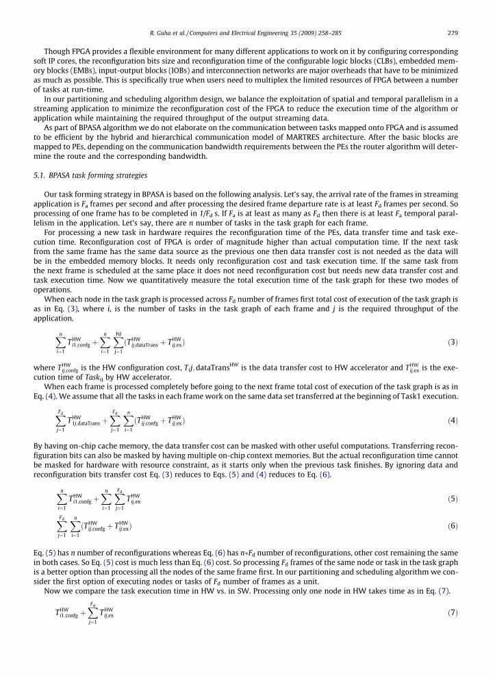
R. Guha et al. / Computers and Electrical Engineering 35 (2009) 258–285 279
Though FPGA provides a flexible environment for many different applications to work on it by configuring correspondingsoft IP cores, the reconfiguration bits size and reconfiguration time of the configurable logic blocks (CLBs), embedded mem-ory blocks (EMBs), input-output blocks (IOBs) and interconnection networks are major overheads that have to be minimizedas much as possible. This is specifically true when users need to multiplex the limited resources of FPGA between a numberof tasks at run-time.
In our partitioning and scheduling algorithm design, we balance the exploitation of spatial and temporal parallelism in astreaming application to minimize the reconfiguration cost of the FPGA to reduce the execution time of the algorithm orapplication while maintaining the required throughput of the output streaming data.
As part of BPASA algorithm we do not elaborate on the communication between tasks mapped onto FPGA and is assumedto be efficient by the hybrid and hierarchical communication model of MARTRES architecture. After the basic blocks aremapped to PEs, depending on the communication bandwidth requirements between the PEs the router algorithm will deter-mine the route and the corresponding bandwidth.
5.1. BPASA task forming strategies
Our task forming strategy in BPASA is based on the following analysis. Let’s say, the arrival rate of the frames in streamingapplication is Fa frames per second and after processing the desired frame departure rate is at least Fd frames per second. Soprocessing of one frame has to be completed in 1/Fd s. If Fa is at least as many as Fd then there is at least Fa temporal paral-lelism in the application. Let’s say, there are n number of tasks in the task graph for each frame.
For processing a new task in hardware requires the reconfiguration time of the PEs, data transfer time and task exe-cution time. Reconfiguration cost of FPGA is order of magnitude higher than actual computation time. If the next taskfrom the same frame has the same data source as the previous one then data transfer cost is not needed as the data willbe in the embedded memory blocks. It needs only reconfiguration cost and task execution time. If the same task fromthe next frame is scheduled at the same place it does not need reconfiguration cost but needs new data transfer cost andtask execution time. Now we quantitatively measure the total execution time of the task graph for these two modes ofoperations.
When each node in the task graph is processed across Fd number of frames first total cost of execution of the task graph isas in Eq. (3), where i, is the number of tasks in the task graph of each frame and j is the required throughput of theapplication.
Xn
i¼1
THWi1;confg þ
Xn
i¼1
XFd
j¼1
ðTHWij;dataTrans þ THW
ij;exÞ ð3Þ
where THWij;confg is the HW configuration cost, Tij;dataTransHW is the data transfer cost to HW accelerator and THW
ij;ex is the exe-cution time of Taskij by HW accelerator.
When each frame is processed completely before going to the next frame total cost of execution of the task graph is as inEq. (4). We assume that all the tasks in each frame work on the same data set transferred at the beginning of Task1 execution.
XFd
j¼1
THW1j;dataTrans þ
XFd
j¼1
Xn
i¼1
ðTHWij;confg þ THW
ij;exÞ ð4Þ
By having on-chip cache memory, the data transfer cost can be masked with other useful computations. Transferring recon-figuration bits can also be masked by having multiple on-chip context memories. But the actual reconfiguration time cannotbe masked for hardware with resource constraint, as it starts only when the previous task finishes. By ignoring data andreconfiguration bits transfer cost Eq. (3) reduces to Eqs. (5) and (4) reduces to Eq. (6).
Xn
i¼1
THWi1;confg þ
Xn
i¼1
XFd
j¼1
THWij;ex ð5Þ
XFd
j¼1
Xn
i¼1
ðTHWij;confg þ THW
ij;exÞ ð6Þ
Eq. (5) has n number of reconfigurations whereas Eq. (6) has n�Fd number of reconfigurations, other cost remaining the samein both cases. So Eq. (5) cost is much less than Eq. (6) cost. So processing Fd frames of the same node or task in the task graphis a better option than processing all the nodes of the same frame first. In our partitioning and scheduling algorithm we con-sider the first option of executing nodes or tasks of Fd number of frames as a unit.
Now we compare the task execution time in HW vs. in SW. Processing only one node in HW takes time as in Eq. (7).
THWi1;confg þ
XFd
j¼1
THWij;ex ð7Þ

280 R. Guha et al. / Computers and Electrical Engineering 35 (2009) 258–285
With the same mode of processing Fd frames first for each task the corresponding software execution time is as in Eq. (8).
XFd
j¼1
TSWij;ex ð8Þ
If there are total F frames to be processed, with our mode of processing Fd frames first for each task as a unit there will betotal n�F/Fd tasks in the task list in comparison to n�F tasks if the frames were processed one by one. Thus by considering Fd
frames as a unit we reduce the number of tasks to be considered by the scheduler in addition to reducing reconfigurationcost of the FPGA.
5.2. BPASA partitioning and scheduling strategies and pseudo code
The first partitioning and scheduling strategy of BPASA is to consider Fd frames as a unit to reduce reconfiguration over-head and to reduce the number of tasks to be considered by the scheduler as explained above.
The second strategy of BPASA is to minimize the fragmentation of the FPGA fabric. The tasks with the same function issized to be as big as a neighborhood size N, by exploiting the spatial concurrency to reduce area fragmentation in a neighbor-hood. N is the neighborhood size in terms of number of PEs. By making a task as big as a neighborhood size the logic and mem-ory resources of a neighborhood is utilized fully and efficiently. If a task cannot be made as big as a neighborhood then it is asmaller task. Tasks are not made bigger than one neighborhood to reduce communication cost. By making the tasks as big as aneighborhood size the number of tasks in the task list is initially small. If a task cannot fit in any of the neighborhoods then thetask can be split between neighborhoods or between hardware and software. Number of tasks generated per basic block inthe task graph is K = BBi/N, where i is the number of the basic block. Taski,k. area = N or less, where i is the number of the basicblock and i = 1 to n and k is the number of tasks for ith basic block and k = 1 to K. The Taski,k is a unit which comprises of Fd
frames of the same basic block i and task k.The third strategy of BPASA is to prepare a task list for the scheduler depending on the following criteria. All basic blocks
BBi where i = 1 to n, having the same earliest start time are grouped together to find the degree of concurrency in differenttime steps. Time_stepl = {BBm, . . . ,BBp; m, p< = n}, whose earliest start time are same or close to each other and l = 1 to L timesteps. Each time step is defined in such a way that there is a distinct demarcation of task start time in each time step, asshown in Fig. 22.
The tasks are sorted in ascending order of the task’s earliest start time. Tasks within the same time step are sorted indescending order of their size or area requirement. In hard real-time systems some tasks may have completion deadlineand so can be given higher priority than the others in the same time step. Within the same time step if two tasks have highcommunication cost their combined size can be considered for placement in contiguous area. The scheduler uses an efficientplacement algorithm HBFA as proposed in Section 4. HBFA algorithm follows hierarchical best fit strategy to check whetheran actual physical placement is possible by the available hardware resources and to reduce area fragmentation. As HBFAalgorithm is faster than traditional BF algorithm, BPASA algorithm in turn works faster. By sorting the tasks in each time stepin descending order of their size, the placement strategy becomes same as best fit descending (BFD) [31] strategy, the off-linevariety of bin packing algorithm. By placing the bigger task at the bottom of the bin or the neighborhood has the advantage ofminimizing the number of bins or area required to place all the tasks.
The fourth strategy of BPASA is to balance the load between SW and HW in terms of total execution time of the SW pro-cessor and the HW accelerator. Even if the hardware execution time of a task is smaller than SW execution time, if the hard-ware is too busy the task will be scheduled for software execution. If two variables HW_Timer and SW_Timer keep the time oftill what time the HW accelerator and SW processor are booked then the scheduling decision for the next task is the min-imum of the HW_Finish_Time andSW_Finish_Time where
HW Finish Time ¼ HW Timer þ Task list½i�:HW EX Time ð9ÞSW Finish Time ¼ SW Timer þ Task list½i�:SW EX Time ð10Þ
Fig. 22. Ordered task list depending on the degree of spatial concurrency in an application.

R. Guha et al. / Computers and Electrical Engineering 35 (2009) 258–285 281
Task_list[i] is the ith task to be considered by the scheduler and HW_EX_Time and SW_EX_Timeare its execution time in HWand SW, respectively.
Every time a task is assigned for SW execution the SW timer is advanced by the SW execution time for that task.HW_Book_Time is another variable which keeps track of how soon some area will be available after a task’s execution.HW_Book_Time is updated with the HW_Finish_Time of a task only if it is less than the value stored in HW_Book_Time. In casethere is no hardware area available immediately it can also check whether waiting for the next available area is better thanscheduling the task for software implementation. Whenever the available hardware area becomes zero the HW_Timer is alsoupdated with the earliest time when some area will be available. If all the tasks in a time step have been scheduled theHW_Timer is advanced to the next time step.
For the very first task HW reconfiguration time and data transfer time are required so those are added for calculating HWexecution time. For each task, data source is checked, if it is dependant on previous task and which is already executed inHW, the data transfer cost is not calculated. For a new task, reconfiguration time is always there. If HW_Finish_Time is lessthan SW_Finish_Time and HW area is available the task is scheduled for HW execution otherwise for SW execution. The as-signed task in SW or HW is removed from the task list. The pseudo code for BPASA is given in Table 12. BPASA is a greedyheuristic algorithm and makes the decision which appears best at that time to reduce the scheduling time. For a dynamictask list and run-time reconfiguration criteria it is important that the scheduling algorithm works faster. Thus BPASA is verysuitable for fast decision making for dynamic environment.
5.3. Simulation results
We have tested our task formation strategy and the partitioning and scheduling algorithm, BPASA, for several streamingapplications like discrete Cosine transform (DCT), 100 Taps FIR Filter and data encryption standards (DES) algorithms com-peting simultaneously for resources on FPGA fabric. In all cases our task formation strategies were feasible and gave muchsuperior performance in terms of FPGA area usage, scheduling algorithm evaluation time and application execution time.
The number of operations to be completed for each algorithm is calculated as follows. A two dimensional DCT algorithmis shown in Table 13. Number of operations in a 2D DCT kernel can be calculated as N�N�N + N�N multiplications and N�N�Nadditions. If N = 8 then for an 8�8 block of image frame there are 8�8�8 + 8�8 = 576 multiplications and 8�8�8 = 512 addi-tions, totaling to 1088 operations. For a 256�256 image frame and for a required throughput of 30 frames per second thenumber of operations that should be completed in one second is (256�256�30�1088/8�8) = 33 M operations.
A N Taps Filter Kernel is shown in Table 14. Number of operations in 100 Tap FIR filter is 100 multiplications and 100additions per data. For a 256�256 image frame and 30 frames per second required throughput the required number of oper-ations that should be completed in one second is 256�256�30�200 = 393 M operations.
Table 12BPASA pseudo code
Create Array Task_list[Task1, Task2. . .Taskn]//sorted in descending order of size in each time stepCreate Array HW_list[]//to identify task for HW executionCreate Array SW_list[]//to identify task for SW executionCreate variable HW_Timer, SW_Timer, HW_Finish_Time[i], SW_Finish_Time[i], Algorithm_Execution_Time, HW_Book_Time, HW_Book_Area, No_of_Try,
Aavailable, Task_Placement //Available HW areaBPASA(Task_list)//minimum execution time partitioning and scheduling algorithmfor i 1 to length[Task_list]HW_Finish_Time[i] = HW_Timer + Task_list [i]. HW_EX_Time;//configuration time and data transfer time included in HW_EX_Time
SW_Finish_Time[i] = SW_Timer + Task_list [i]. SW_EX_Time;if (HW_Finish_Time[i] < = SW_Finish_Time[i])then
if HBFA = SUCCEED//placement algorithm succeeds mapping the task in HWthen APPEND (HW_list, Task_list [i])REMOVE (Task_list, Task_list [i])Aavailable = Aavailable � Task_list[i].areaif HW_Book_Time > HW_Finish_Time[i]then HW_Book_Time = HW_Finish_Time[i]
HW_Book_Area = Task_list[i].areaif Aavailable = 0then HW_Timer = HW_Book_Time
else//try again for next available HW areaHW_Timer = HW_Book_TimeAavailable = Aavailable + HW_Book_AreaNo_of_Try++;if No_of_Try< = 2thenBPASA(Task_list[i])
elseAPPEND (SW_list, Task_list [i])REMOVE (Task_list, Task_list [i])SW_Timer = SW_Finish_Time[i];
Algorithm_Execution_Time = MAX(SW_Timer, HW_Timer);

Table 132-D DCT Kernel
for (i = 0; i < N; i++){for (j = 0; j < N; j++)
{DCTvalues[i][j] = 0;for (k = 0; k < N; k++){DCTvalues[i][j]+ = inputData[i][k]�encode_cos_table[k][j];
}DCTvalues[i][j]� = c_table[i][j];}}
Table 14N tap FIR filter Kernel
for (i = 0; i < N; i++){Y[n]+ = c[i]X[n � i];}
Table 15BPASA results
Algorithms No. of frames Image size Required throughput MOPS Tasks/frame BPASA area utilization (%) Application ex time (s)
DCT 2D 256 256�256 33 M 20 90 9FIR filter (100 taps) 256 256�256 393 M 20DES 256 256�256 40 M 20DCT 2D 512 512�512 133 M 40 93 18FIR filter (100 taps) 512 512�512 1572 M 40DES 512 512�512 158 M 40
282 R. Guha et al. / Computers and Electrical Engineering 35 (2009) 258–285
Data encryption standard (DES) is a very complex algorithm which involves a number of steps. In the first step 16 sub-keys are generated from a 64 bit private key. With this 16 sub-keys each 64 bits of data is coded which also involves manypermutation tables for shuffling the data bits and substitution box (S-Box) to encode the data bits. DES algorithm can be opti-mized by generating the sub-keys once and storing them in the look up tables. All permutation tables and S-Boxes can bestored in SRAM on-chip memory. After all the optimization we can assume there are 16�10 = 160 operations for 64 bitsor 8 pixels of data encoding by 16 sub-keys. For a 256�256 image size with 30 frames per second throughput the numberof operations to be completed in one second is 256�256�30�160/8 = 40 M operations.
Table 15 lists the result of the dynamic task mapping strategies with BPASA algorithm for different number of frames andimage sizes of three different algorithms competing for fixed hardware area. We have simulated our BPASA partitioning andscheduling algorithm for a total hardware resource of 8 neighborhoods each containing 8 PEs and operating at a conservativespeed of 50 MHz.
Tasks from three different algorithms were given equal priorities and chosen in a Round Robin pattern by the BPASAscheduler. Area utilization by the BPASA algorithm depends on number of tasks formed per frame and their respective sizes.Simulation results of BPASA algorithm shows that when the task sizes are larger and close to neighborhood size the area uti-lization is higher than that of the smaller tasks. BPASA algorithm is evaluated in O(n) time where n is the number of tasks inthe task list. Available logic and memory resources of Virtex-5 device were enough for configuration of 8 neighborhoods eachcontaining 8 PEs and all 3 algorithms could complete execution with the required throughput of output data.
In summary we have presented a novel list scheduling algorithm which takes into account configuration time and datatransfer time to balance the spatial and temporal parallelism in a streaming application in the best possible way. As BPASA isa heuristic algorithm it takes less time for run-time partitioning and scheduling decision making and also finds a good solu-tion to the partitioning and scheduling problem. We have heuristically derived every steps of BPASA partitioning and sched-uling algorithm to get a solution whose fitness factor is so good that it need not go through the iterative genetic algorithm forimproving the partitioning and scheduling solution.
6. Conclusions
The primary objective of this research work has been to accelerate high computation-load applications by a reconfigura-ble computing platform. For that purpose we have designed an application configuration architecture for FPGA named MAR-TRES, which is flexible, modular and facilitates power savings by advanced technologies like partial reconfiguration, clockgating and voltage scaling etc. Our task mapping strategy on FPGA has been to confine a task within a local group of PEsto reduce communication overhead. Thus we have designed a hybrid and hierarchical communication network for MARTRESarchitecture where more communication bandwidth is provided within a local group of PEs. When the communication sys-tem is more dedicated within the local group of PEs called block, it is more shared for inter-block and inter- neighborhoodcommunications. By providing a hybrid and hierarchical communication system we have saved on communication resources
R. Guha et al. / Computers and Electrical Engineering 35 (2009) 258–285 283
without sacrificing much on the processing speed and throughput. In MARTRES architecture long bus length has beenavoided for the adverse clock-skew effects.
MARTRES architecture has been designed to facilitate partial run-time reconfiguration and efficient resource manage-ment and resource utilization of the chip. Compact placement of task contributes to power savings, increased multi-taskingand performance improvements of applications. Our dynamic task placement algorithm named HBFA is much faster than thetraditional best fit bin packing algorithm and contributes to performance improvements of the applications. When HBFAplacement algorithm takes O(n) time the corresponding BF algorithm takes O(n2) time. In HBFA, by splitting a task intotwo and placing them within the same neighborhood, area fragmentation of the FPGA fabric has been prevented whileincreasing resource utilization of the chip.
We have also designed a task partitioning and scheduling algorithm. Our task partitioning and scheduling algorithmnamed BPASA balances the exploitation of spatial and temporal parallelism in an application in such a way that the recon-figuration overhead of the chip is reduced while maintaining the required throughput of the output data. In BPASA, if pos-sible each task is sized to the maximum size of a neighborhood of the MARTRES architecture to use the communicationresources of the MARTRES architecture efficiently. Reduction of reconfiguration cost in BPASA algorithm contributes tothe performance improvement of applications.
In conclusion, our work in this paper provides several important contributions in the effort of algorithm acceleration by areconfigurable computing platform. We have quantitatively analyzed the suitability of MARTRES architecture on modernFPGA device platform and the superiority of our placement and partitioning and scheduling algorithms on MARTRES archi-tecture in comparison to other traditional approaches. Our efficient MARTRES configuration architecture and task placementand partitioning and scheduling algorithms contribute to increased resource usage, faster task placement, power savings andperformance improvement of data-intensive streaming applications on modern FPGA device platform.
7. Future work
Both scopes and challenges of reconfigurable computing are enormous. In this paper we have tried to solve only one as-pect of the challenges by designing an efficient application configuration architecture for increased resource utilizationwhich in turn contributes to high performance of applications. Reconfigurable computing being in its early research phasethere are still lack of CAD tools which can synthesis the hardware circuits and software controller from the high-level pro-gramming languages automatically or semi-automatically. In continuation of this present work, as future work we identifythe need for designing an efficient CAD tool which can accelerate task mapping onto FPGA. A mapping library can be createdwhich can produce optimized hardware circuits and software controllers from the functions written in C like programminglanguages. The CAD tool will take less time in searching through the repository of information and coming with a task map-ping solution faster. By using this mapping library the CAD tool should be able to estimate how much hardware resourceswill be required for a given function in terms of logic and memory blocks and interconnect bandwidth and whether thatmuch contiguous area is currently available. As for example for implementing a for loop the CAD tool should be able to esti-mate the amount of parallelism created vs. the execution time of the for loop and then design the corresponding hardwarecircuit according to the available contiguous resources. The CAD tool should also be able to estimate per function executiontime, area requirement and power consumption when implemented on a particular modern FPGA device platform. As futurework we also want to include some efficient design methodologies in our CAD tool for converting a complete applicationwhich was originally meant for sequential execution by a microprocessor to alternative parallel program to be executedby the parallel architecture of the reconfigurable device platform.
References
[1] Boekhorst F. Ambient intelligence, the next paradigm for consumer electronics: how will it affect silicon. In: Proceedings of international solid, statecircuits conference; February 2002. p. 28–31.
[2] ITRS. International technology roadmap for semiconductors; 2005 Edition.[3] Henkel Jörg. Closing the SoC design gap. Computer 2003;36(9):119–21.[4] Heysters P, Smit G, Molenkamp E. A flexible and energy-efficient coarse-grained reconfigurable architecture for mobile systems. J Supercomputing
2003;26(3):283–308.[5] Chen J, Yeh J, Lan Y, Lin L, Chen F, Hung S. RAMP: reconfigurable architecture and mobility platform. In: Proceedings of IEEE Globecom, vol. 6; 2005. p.
3564–9.[6] Banerjee S, Bozorgzadeh E, Dutt N. Physically-aware HW-SW partitioning for reconfigurable architectures with partial dynamic reconfiguration. DAC;
June 2005. p. 335–40.[7] Mei B, Schaumont P, Vernalde S. A hardware–software partitioning and scheduling algorithm for dynamically reconfigurable embedded systems. In:
Proceedings of ProRISC; 2000.[8] Xilinx.Virtex-4 user guide UG070 (v2.2); April 10, 2007.[9] Xilinx. Virtex-5 user guide UG190 (v3.0); February 2, 2007.
[10] Xilinx. Virtex-5 family overview, LX, LXT and SXT platforms. DS100 (V3.2); September 4, 2007.[11] ALTERA. Stratix III TriMatrix Memory. <www.altera.com>; October 2007.[12] Cosoroaba A. Memory interfaces made easy with xilinx fpgas and the memory interface generator. Xilinx WP260 (V1.0); February 16, 2007.[13] Gokhales M, Graham P. Reconfigurable computing: accelerating computation with field-programmable gate arrays. Springer; 2005.[14] Barat F, Lauwereins R. Reconfigurable instruction set processors: a survey. In: Proceedings of the 11th international workshop on rapid system
prototyping (RSP’00); June 2000. p. 168–73.[15] Athens P, Silverman H. Processor reconfiguration through instruction set metamorphosis: architecture and compiler. Computer 1993;26(3):11–8.[16] Callahan, Hauser J, Wawrzynek J. The Garp architecture and C compiler. Computer 2000;33(4):62–9.[17] Arnold J. The splash 2 software environment. In: Proceedings of IEEE symposium on FPGAs for custom computing machines; 1993. p. 88–93.

284 R. Guha et al. / Computers and Electrical Engineering 35 (2009) 258–285
[18] Wan M, Zhang H, George V, Benes M, Abnous A, Prabhu V, et al. Design methodology of a low-energy reconfigurable single-chip dsp system. J VLSISignal Process 2001;28:47–61.
[19] Mirsky E, DeHon A. MATRIX: a reconfigurable computing architecture with configurable instruction distribution and deployable resources. IEEE SympFCCM 1996:157–66.
[20] C, Cronquist D, Franklin P. Configurable computing: the catalyst for high-performance architectures. In: Proceedings of IEEE international conferenceon application specific systems, architectures and processors; 1997. p. 364–72.
[21] Lee M-H, Singh H, Lu G, Bagherzadeh N, Kurdahi F. Design and implementation of the morphosys reconfigurable computing processor. J VLSI SignalProcess 2000;24(2/3):147–64.
[22] Hauck TMiyamori T, Olukotun K A quantitative analysis of reconfigurable coprocessors for multimedia applications In: Proceedings of the IEEEsymposium on field-programmable custom, computing machines; 1998 p 2–11.
[25] Tensilica. Xtensa-7 configurable processor. Tensilica, Inc.; 2006.[26] Bolotin E, Cidon I, Ginosar R, Kolodny A. Cost considerations in network on chip. VLSI J 2004;38:19–42.[27] Arteris. A comparison of network-on-chip and busses. <www.arteris.com>; October 2007.[28] Bertozzi D, Jalabert A, Murali S, Tamhankar R, Stergiou S, BeniniL et al. NoC synthesis flow forcustomized domain specific multiprocessor systems-on-
chip. IEEE Trans Parallel Distributed Syst, vol. 16, no. 2; February 2005.[29] Vahdatpour1 A, Tavakoli2 A, Hossein Falaki1 M. Hierarchical graph: a new cost effective architecture for network on chip. EUC 2005, LNCS 3824
2005:311–20.[30] Bambha N, Bhattacharyya S. Joint application mapping/interconnect synthesis techniques for embedded chip-scale multiprocessors. IEEE Trans
Parallel Distributed Syst 2005;16(2):99–112.[31] Malkevitch J. Bin packing. <www.ams.org>; October 2007.[32] Lee CC, Lee DT. A simple on-line bin-packing algorithm. J Assoc Comput Machinery 1985;32(3):562–72.[33] Goodman ED, Tetelbaum AY, Kureichik VM. A genetic algorithm approach to compaction, bin packing, and nesting problems. Technical report #
940702, case center for computer-aided engineering and manufacturing, Michigan State University.[34] Reeves C. Hybrid genetic algorithms for bin packing and related problems. Published in annals of OR, vol. 63. p. 371–96.[35] Walder H, Steiger C, Platzner M. Fast online task placement on FPGAs: free space partitioning and 2D-hashing. In: Proceedings of the international
parallel and distributed processing symposium (IPDPS’03); April 2003. p. 178.[36] Bazargan, Kastner R, Sarrafzadeh M. Fast template placement for reconfigurable computing systems. IEEE Des Test Comput 2000;17:68–83.[37] de Niz D, Rajkumar R. Partitioning bin-packing algorithms for distributed real-time systems. Int J Embedded Syst 2006;2(3/4):196–208.[38] Wiseman J. An introduction to MPEG video compression. <http://www.john-wiseman.com/technical/MPEG_tutorial.htm>; October 2007.[39] Kernighan B, Lin S. An efficient heuristic procedure for partitioning graphs. Bell Syst Tech J 1970;29:291–308.[40] Banerjee S, Dutt N. Efficient search space exploration for HW-SW partitioning. CODES + ISSS; 2004. p. 122–7.[41] Noguera J, Badia R. A HW/SW partitioning algorithm for dynamically reconfigurable architectures. In: Proceedings of design automation and test in
Europe; 2000. p. 0729.[42] Jeong B, Yoo S, Lee S, Choi K. Hardware software co synthesis for run-time incrementally reconfigurable FPGAs. In: Proceedings of ASP-DAC; 2000. p.
169–74.[43] Mei B, Vernalde S, Verkest D, Lauwereins R. Design methodology for a tightly coupled VLIW/reconfigurable matrix architecture: a case study. In:
Proceedings of the design, automation and test in Europe conference and exhibition (DATE’04)P; 2004. p. 1224–9.[44] Mei B, Vernalde S, Verkest D, Man H, Lauwereins R. ADRES: an architecture with tightly coupled vliw processor and coarse-grained reconfigurable
matrix. In: 13th international conference on field programmable logic and applications, vol. 2778; 2003. p. 61–70.[45] Tiwari A, Tomko KA. Saving power bymapping finite-state machines intoembedded memory blocks in FPGAs. In: Proceedings design, automation and
test in Europe conference and exhibition, vol. 2; February 2004. p. 916–21.[46] Oliver J, Rao R, Sultana P, Crandall J, Czernikowski E, Jones LW IV, Franklin D, Akella V, Chong FT. Synchroscalar:a multiple clock domain, power-aware,
tile-based embedded processor. In: International symposium on computer architecture; June 2004. p. 150–61.[47] Cormen T, Leiserson C, Rivest R, Stein C. Introduction to algorithms. India: Prentice Hall; 2003.
Dr. Radha Guha, Associate Professor, Computer Science and Engineering, Amrita University, Coimbatore, India.She has received the Doctorate Degree in Computer Systems and Software from the EECS Department of University of
California, Irvine in December 2007. Her research interest is mainly in efficient embedded system architecture design foralgorithm acceleration by the reconfigurable computing platform of field programmable gate arrays (FPGAs) for the high-performance computation-loads. Before joining the academia she has also worked as a software system engineer and as anelectrical engineer for several years.
Dr. Nader Bagherzadeh, Professor, Electrical Engineering and Computer Science University of California, Irvine.He is interested in low-power and embedded digital signal processing, computer architecture, computer graphics and VLSI
design. Within the area of embedded digital signal processing, Dr. Bagherzadeh is interested in the design and VLSI developmentof reconfigurable processor architectures and their algorithm mapping for high-performance and low-power applications inmobile communications. This technology can be used for 3G and 4G cellular phones, as well as other telecommunicationssystems. In the area of computer graphics, Dr. Bagherzadeh has been involved in the development of a new scheme for creatingcomputer-generated three-dimensional models of a scene based on previously recorded images captured with a standard digitalvideo camera. These models can be used for military and civilian simulator applications, as well as movie special effects. In thearea of low-power system design, Dr. Bagherzadeh has developed a software tool for scheduling and planning mission tasks toachieve power and performance objectives. This technology is targeted for planetary missions of autonomous spacecraft as wellas for unmanned military vehicles.
Dr. Pai Chou, Associate Professor, Electrical Engineering and Computer Science University of California, Irvine.He is interested in hardware and software co-design, power-aware and adaptive embedded systems, system synthesis, and
embedded instruments. He has been developing integrated management power-aware computing and communication tech-nologies (IMPACCT), a computer-aided design (CAD) tool for exploring power management policies at the application andarchitecture levels. The goal of the project is to improve power and performance for mission-critical systems, including the MarsRover project by NASA/JPL and Rockwell Collin’s software defined radio systems. Dr. Chou is currently developing a number ofembedded instruments. One is the B# battery emulator, which is a smart power supply that mimics the power output of abattery. Another embedded instrument is the mini-FDPM breast cancer detector in collaboration with the Beckman LaserInstitute. He is also building wireless sensor nodes for monitoring structural health of building structures.
R. Guha et al. / Computers and Electrical Engineering 35 (2009) 258–285 285


