Embed Size (px)
Citation preview
May 15, 2014 16:32 WSPC/147-MPLB S0217984914500961 1–10
Modern Physics Letters BVol. 28, No. 12 (2014) 1450096 (10 pages)c© World Scientific Publishing Company
DOI: 10.1142/S0217984914500961
Resistive characteristics of LSMO/LCMO bi-layers and temperature
switching effect of magnetoresistance
Blagoy S. Blagoev∗ and Timerfayaz C. Nurgaliev†
Institute of Electronics, Bulgarian Academy of Sciences,72 Tzarigradsko Chaussee Blvd., 1784 Sofia, Bulgaria
∗blago [email protected]†[email protected]
Irina E. Bineva
Institute of Solid State Physics, Bulgarian Academy of Sciences,72 Tzarigradsko Chaussee Blvd., 1784 Sofia, Bulgaria
Elmira D. Vasileva
Institute of Electronics, Bulgarian Academy of Sciences,72 Tzarigradsko Chaussee Blvd., 1784 Sofia, Bulgaria
elmira [email protected]
Vladimir Strbik
Institute of Electrical Engineering, Slovak Academy of Sciences,Dubravska cesta 9, 84104 Bratislava, Slovak Republic
Emil S. Mateev
Institute of Electronics, Bulgarian Academy of Sciences,72 Tzarigradsko Chaussee Blvd., 1784 Sofia, Bulgaria
Received 17 February 2014Revised 10 April 2014Accepted 11 April 2014Published 14 May 2014
Ferromagnetic La0.7Sr0.3MnO3/La0.7Ca0.3MnO3 (LSMO/LCMO) bi-layers of submi-cron thickness were deposited by magnetron sputtering on SrTiO3 (STO) and Al2O3
(ALO) substrates and temperature dependence of their resistances were investigated.The samples grown on ALO substrates demonstrated lower metal–insulator transitiontemperatures and higher resistances. The maximum magnetoresistance (MR) of bi-layergrown on STO substrate reached −56% at 184.6 K and magnetic field of 1 T. At tem-peratures below 150 K a “switching” of MR from negative to positive values (+ 1.7% at110 K) and a hysteretic behavior of the resistance at low magnetic fields were observedas well.
1450096-1
May 15, 2014 16:32 WSPC/147-MPLB S0217984914500961 2–10
B. S. Blagoev et al.
Keywords: LSMO/LCMO bi-layer; positive and negative magnetoresistance; switchingof magnetoresistance.
1. Introduction
In the last decades there has been an increasing interest in doped lanthanum man-
ganite oxides (La1−xMxMnO3, M = Sr, Ca, Pb, etc.) because of the richness of
their physical properties resulting from the interplay and competition between
their spin, charge and lattice parameters. The full spin polarization of the charge
carriers and high magneto-resistance (MR) of manganite films make them highly
important for electronic and spintronic applications. Some of the most performed
investigations have been connected with the determination of the structural and
physical properties of La1−xSrxMnO3 (LSMO) and La1−xCaxMnO3 (LCMO) films
grown on different substrates. The structural, magnetic and resistivity properties of
LSMO/LCMO bi-layers have been discussed in literature1–5 too. The temperature
dependence of magnetization and magnetic hysteresis loop of such samples demon-
strate simultaneous response of the both LSMO and LCMO layers. The resistance
and magneto-resistance of LSMO/LCMO bi-layers1–4 have been measured mainly
by placing ohmic contacts on the top layer of the structure. The observed change
of resistivity in the top layer has been interpreted as an effect due to a smaller mis-
match between LSMO and LCMO (and reduced mechanical strains respectively)
than that incoming between the single LSMO or LCMO films and the standard
substrates (LaAlO3, SrTiO3 or NdGaO3).
It is known that the resistance of metals decreases if magnetic field is applied
perpendicularly to the current (negative magneto-resistance — NMR) while in par-
allel configuration the resistance increases (positive magneto-resistance — PMR).6
This effect is referred to as anisotropic magnetoresistance (AMR). Its origin is con-
nected with spin-orbit coupling and spin anisotropy.7,8 It has been found that in
(110) LCMO films in perpendicular magnetic field NMR is observed when the cur-
rent is flowing along the [001] direction and PMR — along [1–10] direction.8 Hybrid
LSMO-STO-Fe junctions have shown a tendency to switch from positive to negative
MR with increasing of the temperature.9
In this study, we present resistivity investigations of ferromagnetic La0.7Sr0.3-
MnO3/La0.7Ca0.3MnO3 bi-layers prepared on SrTiO3 and sapphire (Al2O3)
substrates. In La0.7Sr0.3MnO3/La0.7Ca0.3MnO3 bi-layer deposited on STO, a
“switching” of MR from positive to negative values with the increase of tempera-
ture was observed. The “switching” effect was observed when the measuring elec-
trical current path includes the LSMO, LCMO film areas and the LSMO/LCMO
interface.
2. Experimental Details
The submicron LSMO/LCMO bi-layer were prepared on 0.5 × 5 × 10 mm3 single
crystalline (100) SrTiO3 (STO) and r-cut (−1012) Al2O3 (ALO or sapphire) sub-
1450096-2

May 15, 2014 16:32 WSPC/147-MPLB S0217984914500961 3–10
Resistive characteristics of LSMO/LCMO bi-layers
strates by RF off-axis magnetron sputtering at the deposition conditions close to
those described in Refs. 10–12. First, the bottom LCMO film was deposited. The
top LSMO film was deposited only onto the half surface area of the bottom LCMO
film (see the inset of Fig. 2(a)). The thicknesses of the LSMO and LCMO films were
35/35 nm in bi-layers SA (grown on STO) and SB (grown on ALO), and 35/60 nm
— in bi-layer SD (grown on STO).
X-ray diffraction (XRD) analysis was performed with a HZG4 diffractometer.
For characterization of the LSMO film surface an Atomic Force Microscopy (AFM),
investigations were performed using Multimode AFM instrument with Nanoscope
V controller (Veeco Instruments, Santa Barbara, CA).
Magneto-resistive properties of samples were investigated using PPMS R©
(Physical Property Measurement System). The resistance versus temperature
(10–300 K) R(T ) dependence was obtained using standard four probe method in
three different areas of the samples SA and SB: area AR1 containing LSMO/LCMO
bi-layer (measuring 4 ohmic contacts were placed on the top LSMO layer); area AR2
containing single LCMO layer (measuring 4 ohmic contacts were placed on the bare
LCMO layer); and central area AR3 containing a part of the LSMO/LCMO bi-layer
area and a part of the LCMO single layer area (the ohmic contacts were placed so
that the measuring current pass through LSMO, LCMO areas and LSMO/LCMO
interface — see the inset of Fig. 2(a)). For SD sample, an AR3 measuring scheme
was used only. The resistance versus temperature R(T ) measurements were per-
formed at magnetic fields 0 T and 1 T. The resistance versus magnetic field
(−1 < μ0H < 1 T) R(μ0H) measurements were performed at temperatures 90 K,
110 K, 185 K, 200 K and 300 K. The magnetic field was applied perpendicularly to
the film surface.
3. Results and Discussion
3.1. Structural characteristics and resistance of the samples
The above deposition conditions provide an epitaxial growth of LSMO and LCMO
films on single crystalline STO substrates. Contrariwise, the films sputtered onto
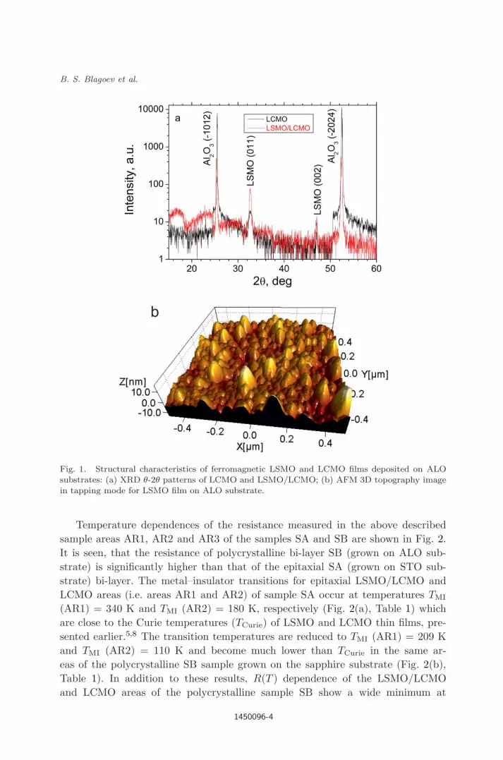
ALO substrates are polycrystalline (Fig. 1). From XRD analysis (Fig. 1(a)), two
different crystallography orientations of ferromagnetic films (011) and (002) could
be distinguished. The peaks of LCMO(011) and LSMO/LCMO(011) are at the
same 2θ position while the peak of LSMO/LCMO(002) is positioned at smaller
2θ value than the peak of LCMO(002). AFM analysis of the 35 nm LSMO film
deposited on ALO substrate shows predominantly distribution of small grains with
60–70 nm diameters (Fig. 1(b)). There are also separate grains with double or larger
dimensions due to a coalescence of smaller grains. Such kind of the film structure
is characteristic for the Volmer–Weber type growth mechanism of films with 3D
islands where the interactions between adatoms are stronger than those of adatoms
with the substrate surface.
1450096-3
May 15, 2014 16:32 WSPC/147-MPLB S0217984914500961 4–10
B. S. Blagoev et al.
Fig. 1. Structural characteristics of ferromagnetic LSMO and LCMO films deposited on ALOsubstrates: (a) XRD θ-2θ patterns of LCMO and LSMO/LCMO; (b) AFM 3D topography imagein tapping mode for LSMO film on ALO substrate.
Temperature dependences of the resistance measured in the above described
sample areas AR1, AR2 and AR3 of the samples SA and SB are shown in Fig. 2.
It is seen, that the resistance of polycrystalline bi-layer SB (grown on ALO sub-
strate) is significantly higher than that of the epitaxial SA (grown on STO sub-
strate) bi-layer. The metal–insulator transitions for epitaxial LSMO/LCMO and
LCMO areas (i.e. areas AR1 and AR2) of sample SA occur at temperatures TMI
(AR1) = 340 K and TMI (AR2) = 180 K, respectively (Fig. 2(a), Table 1) which
are close to the Curie temperatures (TCurie) of LSMO and LCMO thin films, pre-
sented earlier.5,8 The transition temperatures are reduced to TMI (AR1) = 209 K
and TMI (AR2) = 110 K and become much lower than TCurie in the same ar-
eas of the polycrystalline SB sample grown on the sapphire substrate (Fig. 2(b),
Table 1). In addition to these results, R(T ) dependence of the LSMO/LCMO
and LCMO areas of the polycrystalline sample SB show a wide minimum at
1450096-4

May 15, 2014 16:32 WSPC/147-MPLB S0217984914500961 5–10
Resistive characteristics of LSMO/LCMO bi-layers
Fig. 2. Temperature dependence of the resistance for bi-layers SA (a) and SB (b), measured inthe sample areas AR1 (1, circles), AR2 (2, circles) and AR3 (3, stars). The ohmic contact positionsfor resistivity measurement of the central area AR3 and the orientation of applied magnetic fieldare shown in Fig. 2(a) inset.
Tmin (AR1, AR2) = 40 K which is possibly due to Coulomb blockade effect13,14
or to the effect of reduction of ferromagnetic spin ordering at the grain bound-
aries.15 Such upturn at low temperatures is typical for polycrystalline manganites
and is extensively investigated elsewhere.10,13–15
Temperature dependences of the resistance, measured in area AR3 (which is the
series “connected” resistances of LSMO film, LSMO/LCMO interface and LCMO
film, see the inset of Fig. 2(a)) of LSMO/LCMO bi-layers SA and SB are shown
1450096-5

May 15, 2014 16:32 WSPC/147-MPLB S0217984914500961 6–10
B. S. Blagoev et al.
Table 1. Parameters of LSMO (35 nm)/LCMO (35 nm) bi-layers SA and SB.
Sample, substrate Areas of the bi-layer TMI, K Rmax, kΩ Tmin, K Rmin, kΩ
AR1 340 1.9 — —
SA, STO AR2 180 97 — —
AR3 152 227 — —
AR1 209 27 40 11
SB, ALO AR2 110 6316 40 3362
AR3 150 1076 40 378
in Fig. 2 as well. It is interesting to note that the temperature of metal–insulator
transition, measured by such way (AR3) is nearly the same for the bi-layers SA and
SB (TMI ∼ 150 K) although the resistance is about five times greater for the poly-
crystalline bi-layer SB (Fig. 2, Table 1). The area AR3 of bi-layer SA demonstrates
a lower transition temperature TMI and a higher value of the maximum resistance
Rmax as compared with TMI and Rmax of AR1 and AR2 areas of the same sample
(Fig. 2(a)). This difference of the parameters could be due to a poorer crystalline
structure of the bi-layer, especially at the interphase area. TMI and Rmax of AR3
area of polycrystalline sample SB, deposited on ALO are characterized with inter-
mediate positions, placed between TMI and Rmax of AR1 and AR2 areas of the
sample (Fig. 2(b)). The change of TMI and Rmax in this case is partly due to a
significantly lower resistance of LSMO film in comparison with the resistance of
LCMO layer (by two orders of magnitude) at the temperature range 100 K–300 K.
Therefore the measuring current passes a longer part of the “path” through the
LSMO component of the bi-layer than through its LCMO component.
3.2. Magnetoresistance of LSMO/LCMO bi-layer grown on STO
The magnetoresistance effect was investigated in AR3 area of the epitaxial SD bi-
layer which contained a thicker LSMO layer. The measuring scheme was the same
as that shown in the Fig. 2(a) inset. According to obtained results, the sample SD
was characterized by higher temperature of metal–insulator transition TMI ∼ 198 K
and by lower value of maximum resistance Rmax ∼ 24 kΩ in comparison with the
sample SA (Figs. 2(a) and 3, Tables 1 and 2). The external DC magnetic field of
1 T led to increasing of TMI from ∼198 K to ∼ 208 K and to decreasing of Rmax
from 24 kΩ to 17 kΩ. The temperature dependence of magnetoresistance of the
sample, calculated by MR = 100× [R(1 T) −R(0 T)]/R(0 T) formula is presented
in Fig. 3. The magnetoresistance is negative and reaches −56% at magnetic field
μ0H = 1 T and temperature T = 184.6 K (Fig. 3, Table 2). It is interesting to note
that at lower temperatures (below 150 K) a “switching” of the magnetoresistance
from the negative to the positive values can be observed (i.e. the negative MR effect
is transformed to a positive one) (Fig. 3, inset).
1450096-6

May 15, 2014 16:32 WSPC/147-MPLB S0217984914500961 7–10
Resistive characteristics of LSMO/LCMO bi-layers
Fig. 3. Temperature dependences of the resistance and magnetoresistance (MR) of the area AR3of as-deposited sample SD. The inset shows an enlargement of MR versus T dependence below150 K where the MR changes its sign from negative to positive.
Table 2. Parameters of LSMO/LCMO bi-layer SD.
TMI, K Rmax, kΩ TMI, K Rmax, kΩ
μ0H = 0 μ0H = 0 μ0H = 1 T μ0H = 1 T TMRmax, K MR, %
As deposited 198.3 24.2 208.25 17.4 184.6 −56
10 months later 196.6 26.3 206.7 18.9 184.1 −54.5
Concerning the time stability of resistivity and magnetoresistivity of sample SD,
their changes remained less than 2% (Table 2) after 10 months keeping the sample
in dry atmosphere.
Decreasing of the resistance R with increasing of magnetic field induction
μ0H , typical for a negative MR effect, was observed at temperatures 185–200 K
(Fig. 4(a) and 4(c)). At lower temperatures (90 K, 110 K), the resistance increases
with increasing the field induction which is characteristic for a positive MR effect
(Fig. 4(b)). The positive MR effect is quite small and its maximal value is + 1.7%
at 110 K. In this temperature range, R versus μ0H dependence demonstrates a
hysteretic behavior with respect to the applied field direction. Figure 4(b) shows
the results of three turns in R(μ0H) measurements: first — field is changed from 0
to 1 T; second — from 1 to −1 T; and third — from −1 to 1 T. It is seen that the
minimum of resistance measured at 110 K for second and third turns is coming not
at zero magnetic fields. The resistive hysteresis loop is “opened” approximately at
± 350 mT. Such a hysteresis is due to the spin-dependent current flowing through
the bi-layer containing LSMO, LCMO film areas and LSMO/LCMO interface.
There is no hysteresis at temperatures above 150 K but another interesting
effect, related to deviation in the maximum resistance near to zero magnetic fields
1450096-7

May 15, 2014 16:32 WSPC/147-MPLB S0217984914500961 8–10
B. S. Blagoev et al.
Fig. 4. Magnetic field dependence of the resistance for SD sample (area AR3) obtained at varioustemperatures. The inset of Fig. 4(c) shows an enlargement of R versus μ0H dependence aroundzero magnetic field.
1450096-8

May 15, 2014 16:32 WSPC/147-MPLB S0217984914500961 9–10
Resistive characteristics of LSMO/LCMO bi-layers
(see the inset of Fig. 4(c)) is observed in different oscillation periods of the external
field. These deviations were found to reach up to 0.4% and 0.06% at 185 K and
300 K, respectively. The standard deviations of resistance at 185 K and 300 K
were by one order of magnitude smaller than the measured deviations of maximum
resistance and this confirm a real existence of deviations. These deviations could
be caused by difference in the conductivity of bi-layer SD (induced, for example by
slight differences in the positions of domain walls in the sample such as in the case
of magnetic training effect16,17) in different turns of the external magnetic field.
4. Conclusion
Ferromagnetic LSMO/LCMO bi-layers were grown on STO and ALO substrates
by RF magnetron sputtering and the temperature and magnetic field dependences
of their resistance were investigated. The bi-layers grown on ALO substrates were
polycrystalline and their metal–insulator transition temperatures were lower (and
the resistances were higher) in comparison with those of the films grown on STO
substrates. The NMR effect observed in bi-layer grown on STO substrate reached
−56% at 184.6 K at magnetic field 1 T. At lower temperatures below 150 K, a
“switching” of MR from negative to positive values (reaching +1.7% at 110 K at
field 1 T) was observed as well. The field dependence of the resistance demonstrated
a hysteretic behavior with respect to the applied field direction. This hysteresis
could be caused by spin dependent current flowing through the bi-layer.
Acknowledgment
This work was supported by the project VEGA 2/0173/13.
References
1. D.-W. Kim, T. W. Noh, H. Tanaka and T. Kawai, Solid State Commun. 125 (2003)305.
2. S. Y. Park, Y. P. Lee and V. G. Prokhorov, J. Korean Phys. Soc. 45 (2004) 47.3. J.-F. Feng, K. Zhao, Y.-H. Huang, J.-G. Zhao, X.-F. Han, W.-S. Zhan and H.-K.
Wong, Chin. Phys. 14 (2005) 1879.4. M. Jain, P. Shukla, Y. Li, M. F. Hundley, H.-Y. Wang, S. R. Foltyn, A. K. Burrell,
T. M. McCleskey and Q. Jia, Adv. Mater. 18 (2006) 2695.5. T. Nurgaliev, U. Topal, B. Blagoev and E. Mateev, J. Supercond. Nov. Magn. 25
(2012) 2495–2498.6. W. Thomson, Proc. Roy. Soc. Lond. 8 (1856–1857) 546.7. I. Rhee and C. Kim, J. Korean Phys. Soc. 38 (2001) 65.8. I. C. Infante, (001) and (110) La2/3Ca1/3MnO3 epitaxial ferromagnetic electrodes:
a comparative study, Ph.D. dissertation, Programa de Doctorat en Ciencia deMaterials, Departament de Fısica Facultat de Ciencies, Universitat Autonomade Barcelona, Barcelona (2008), http://www.tdx.cat/bitstream/handle/10803/3407/ici1de1.pdf?sequence=1.
9. J. Z. Sun, Physica C 350 (2001) 215.
1450096-9

May 15, 2014 16:32 WSPC/147-MPLB S0217984914500961 10–10
B. S. Blagoev et al.
10. B. Blagoev, E. Mateev, V. Strbik, T. Nurgaliev and L. S. Uspenskaya, J. Phys.: Conf.Series 223 (2010) 012015.
11. E. Vlakhov, B. Blagoev, E. Mateev, L. Neshkov, T. Nurgaliev, L. Lakov, K. Toncheva,Y. Marinov, K. Nenkov, I. Radulov, K. Piotrowski, W. Paszkowicz, A. Szewczyk,M. Baran and R. Szymczak, J. Optoelectron. Adv. Mater. 9 (2007) 456.
12. V. Strbık, S. Benacka, E. Mateev, B. Blagoev, T. Nurgaliev and S. Miteva, J. Phys.:Conf. Series 223 (2010) 012044.
13. Y. G. Zhao, W. Cai, X. S. Wu, X. P. Zhang, K. Wang, S. N. Gao, L. Lu and J. Zhu,Appl. Phys. A 81 (2005) 607.
14. M. Garcıa-Hernandez, F. Guinea, A. de Andres, J. L. Martınez, C. Prieto andL. Vazquez, Phys. Rev. B 61 (2000) 9549.
15. S. Y. Yang, W. L. Kuang, Y. Liou, W. S. Tse, S. F. Lee and Y. D. Yao, J. Magn.Magn. Mater. 268 (2004) 326.
16. B. S. Blagoev, S. D. Terzieva, T. K. Nurgaliev, B. L. Shivachev, A. J. Zaleski, V. Mikli,A. D. Staneva and A. K. Stoyanova-Ivanova, J. Magn. Magn. Mater. 329 (2013) 34.
17. V. Markovich, E. S. Vlakhov, Y. Yuzhelevskii, B. Blagoev, K. A. Nenkov andG. Gorodetsky, Phys. Rev. B 72 (2005) 134414.
1450096-10


