Embed Size (px)
Citation preview
TM 11-6625-351-35D E P A R T M E N T O F T H E A R M Y T E C H N I C A L M A N U A L
FIELD AND DEPOTMAINTENANCE MANUAL
RADIO INTERFERENCEMEASURING SET AN/URM-85
This copy is a reprint which includes currentpages from Changes 2 through 4
HEADQUARTERS, DEPARTMENT OF THE ARMY15 MARCH 1962
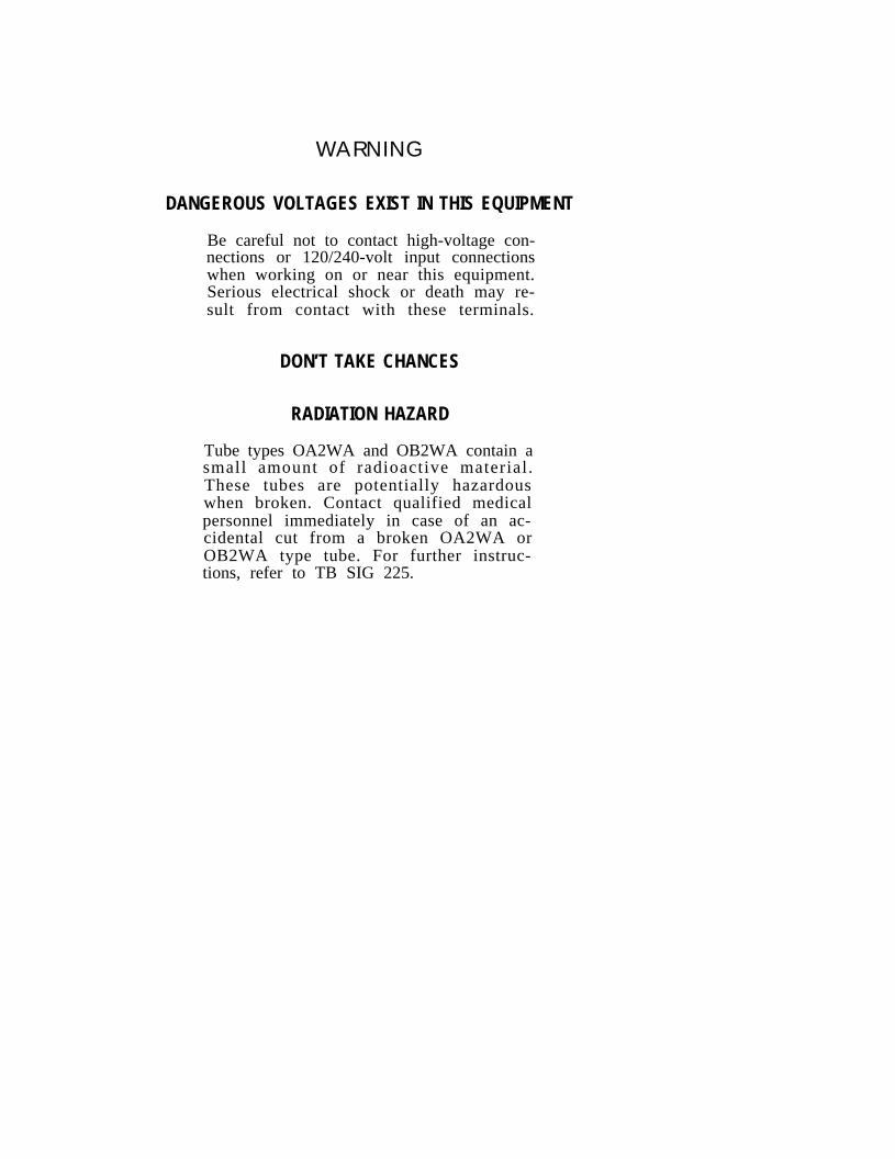
WARNING
DANGEROUS VOLTAGES EXIST IN THIS EQUIPMENT
Be careful not to contact high-voltage con-nections or 120/240-volt input connectionswhen working on or near this equipment.Serious electrical shock or death may re-sult from contact with these terminals.
DON’T TAKE CHANCES
RADIATION HAZARD
Tube types OA2WA and OB2WA contain asmall amount of radioactive material.These tubes are potentially hazardouswhen broken. Contact qualified medicalpersonnel immediately in case of an ac-cidental cut from a broken OA2WA orOB2WA type tube. For further instruc-tions, refer to TB SIG 225.
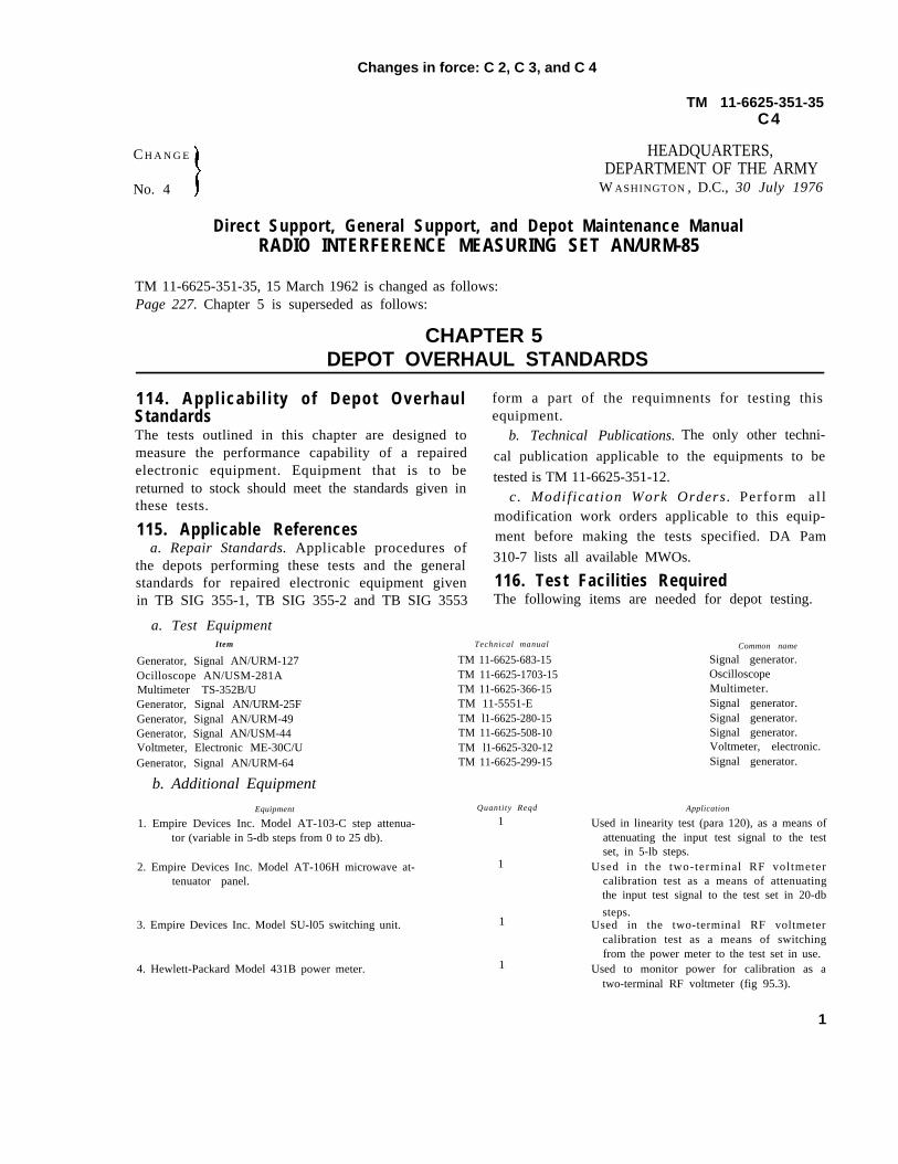
C H A N G E
No. 4
Changes in force: C 2, C 3, and C 4
TM 11-6625-351-35C4
HEADQUARTERS,DEPARTMENT OF THE ARMY
W ASHINGTON , D.C., 30 July 1976
Direct Support, General Support, and Depot Maintenance ManualRADIO INTERFERENCE MEASURING SET AN/URM-85
TM 11-6625-351-35, 15 March 1962 is changed as follows:Page 227. Chapter 5 is superseded as follows:
CHAPTER 5DEPOT OVERHAUL STANDARDS
114. Appl icabi l i ty o f Depot OverhaulStandardsThe tests outlined in this chapter are designed tomeasure the performance capability of a repairedelectronic equipment. Equipment that is to bereturned to stock should meet the standards given inthese tests.
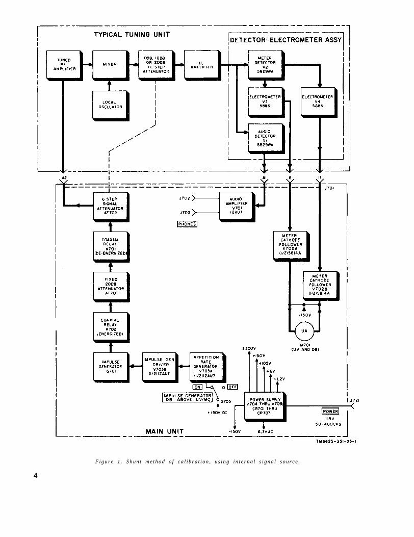
115. Applicable Referencesa. Repair Standards. Applicable procedures of
the depots performing these tests and the generalstandards for repaired electronic equipment givenin TB SIG 355-1, TB SIG 355-2 and TB SIG 3553
Item
a. Test Equipment
Generator, Signal AN/URM-127Ocilloscope AN/USM-281AMultimeter TS-352B/UGenerator, Signal AN/URM-25FGenerator, Signal AN/URM-49Generator, Signal AN/USM-44Voltmeter, Electronic ME-30C/UGenerator, Signal AN/URM-64
b. Additional Equipment
Equipment
1. Empire Devices Inc. Model AT-103-C step attenua-tor (variable in 5-db steps from 0 to 25 db).
2. Empire Devices Inc. Model AT-106H microwave at-tenuator panel.
Technical manual
Quantity Reqd
1
1
3. Empire Devices Inc. Model SU-l05 switching unit. 1
4. Hewlett-Packard Model 431B power meter.
form a part of the requimnents for testing thisequipment.
b. Technical Publications. The only other techni-
cal publication applicable to the equipments to be
tested is TM 11-6625-351-12.c. Modif icat ion Work Orders. Perform al l
modification work orders applicable to this equip-ment before making the tests specified. DA Pam
310-7 lists all available MWOs.
116. Test Facilities RequiredThe following items are needed for depot testing.
TM 11-6625-683-15TM 11-6625-1703-15TM 11-6625-366-15TM 11-5551-ETM l1-6625-280-15TM 11-6625-508-10TM l1-6625-320-12TM 11-6625-299-15
Common name
Signal generator.OscilloscopeMultimeter.Signal generator.Signal generator.Signal generator.Voltmeter, electronic.Signal generator.
Application
Used in linearity test (para 120), as a means ofattenuating the input test signal to the testset, in 5-lb steps.
Used in the two-terminal RF voltmetercalibration test as a means of attenuatingthe input test signal to the test set in 20-db
steps.Used in the two-terminal RF voltmeter
calibration test as a means of switchingfrom the power meter to the test set in use.
Used to monitor power for calibration as atwo-terminal RF voltmeter (fig 95.3).
1
1
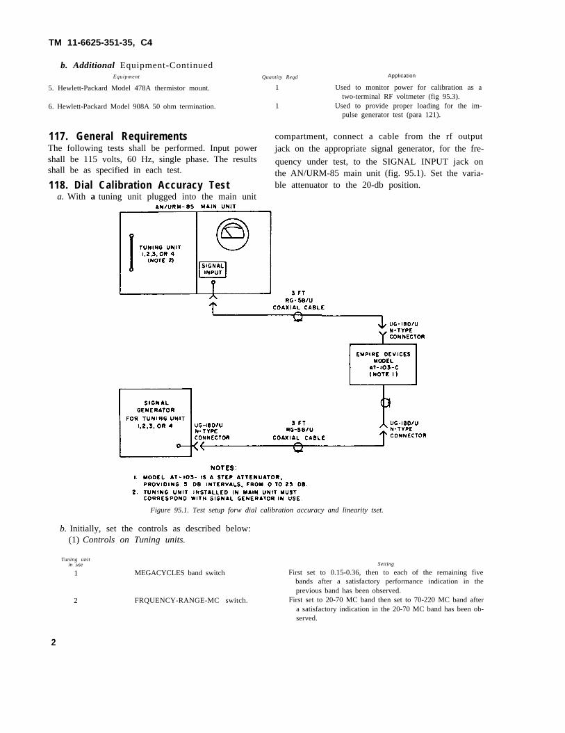
TM 11-6625-351-35, C4
b. Additional Equipment-ContinuedEquipment Quantity Reqd Application
5. Hewlett-Packard Model 478A thermistor mount. 1 Used to monitor power for calibration as atwo-terminal RF voltmeter (fig 95.3).
6. Hewlett-Packard Model 908A 50 ohm termination. 1 Used to provide proper loading for the im-pulse generator test (para 121).
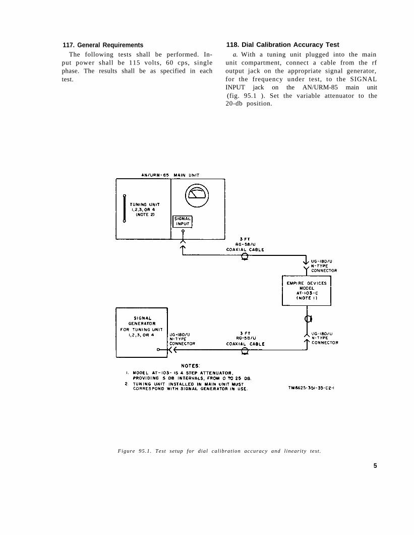
117. General Requirements compartment, connect a cable from the rf outputThe following tests shall be performed. Input power jack on the appropriate signal generator, for the fre-shall be 115 volts, 60 Hz, single phase. The results quency under test, to the SIGNAL INPUT jack onshall be as specified in each test. the AN/URM-85 main unit (fig. 95.1). Set the varia-118. Dial Calibration Accuracy Test ble attenuator to the 20-db position.
a. With a tuning unit plugged into the main unit
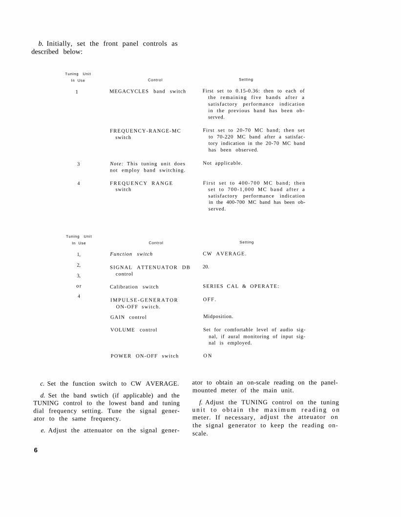
2
Figure 95.1. Test setup forw dial calibration accuracy and linearity tset.
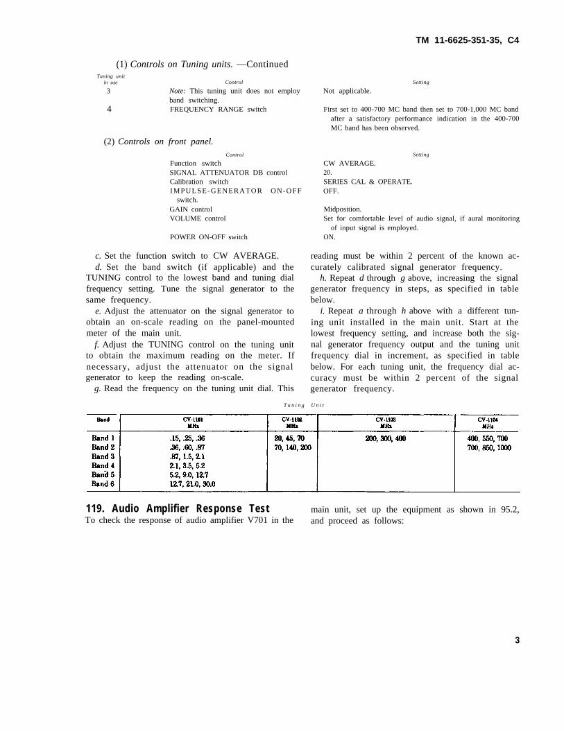
b. Initially, set the controls as described below:(1) Controls on Tuning units.
Tuning unitin use
1 MEGACYCLES band switch
2 FRQUENCY-RANGE-MC switch.
Setting
First set to 0.15-0.36, then to each of the remaining fivebands after a satisfactory performance indication in theprevious band has been observed.
First set to 20-70 MC band then set to 70-220 MC band aftera satisfactory indication in the 20-70 MC band has been ob-served.
TM 11-6625-351-35, C4
(1) Controls on Tuning units. —ContinuedTuning unit
in use
3
4
Control
Note: This tuning unit does not employband switching.FREQUENCY RANGE switch
(2) Controls on front panel.Control
Function switchSIGNAL ATTENUATOR DB controlCalibration switchIMPULSE-GENERATOR ON-OFF
switch.GAIN controlVOLUME control
POWER ON-OFF switch
c. Set the function switch to CW AVERAGE.d. Set the band switch (if applicable) and the
TUNING control to the lowest band and tuning dialfrequency setting. Tune the signal generator to thesame frequency.
e. Adjust the attenuator on the signal generator toobtain an on-scale reading on the panel-mountedmeter of the main unit.
f. Adjust the TUNING control on the tuning unitto obtain the maximum reading on the meter. Ifnecessary, adjust the attenuator on the signalgenerator to keep the reading on-scale.
g. Read the frequency on the tuning unit dial. This
Setting
Not applicable.
First set to 400-700 MC band then set to 700-1,000 MC bandafter a satisfactory performance indication in the 400-700MC band has been observed.
Setting
CW AVERAGE.20.SERIES CAL & OPERATE.OFF.
Midposition.Set for comfortable level of audio signal, if aural monitoring
of input signal is employed.ON.
reading must be within 2 percent of the known ac-curately calibrated signal generator frequency.
h. Repeat d through g above, increasing the signalgenerator frequency in steps, as specified in tablebelow.
i. Repeat a through h above with a different tun-ing unit installed in the main unit. Start at thelowest frequency setting, and increase both the sig-nal generator frequency output and the tuning unitfrequency dial in increment, as specified in tablebelow. For each tuning unit, the frequency dial ac-curacy must be within 2 percent of the signalgenerator frequency.
T u n i n g U n i t
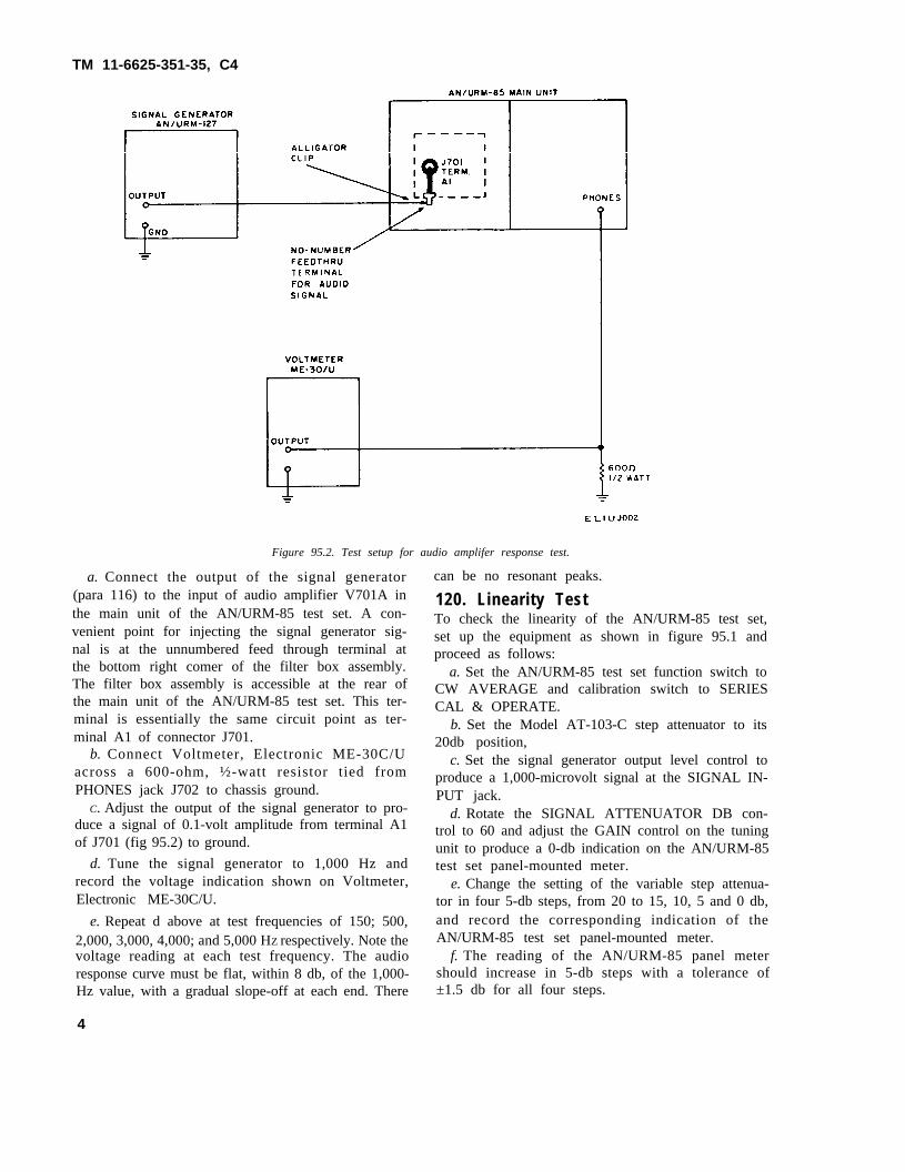
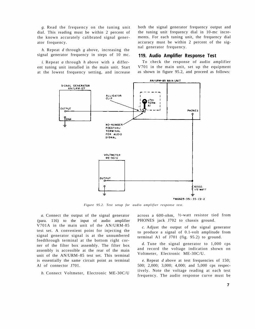
119. Audio Amplifier Response Test main unit, set up the equipment as shown in 95.2,To check the response of audio amplifier V701 in the and proceed as follows:
3
TM 11-6625-351-35, C4
Figure 95.2. Test setup for audio amplifer response test.
a. Connect the output of the signal generator(para 116) to the input of audio amplifier V701A inthe main unit of the AN/URM-85 test set. A con-venient point for injecting the signal generator sig-nal is at the unnumbered feed through terminal atthe bottom right comer of the filter box assembly.The filter box assembly is accessible at the rear ofthe main unit of the AN/URM-85 test set. This ter-minal is essentially the same circuit point as ter-minal A1 of connector J701.
b. Connect Voltmeter, Electronic ME-30C/Uacross a 600-ohm, ½-watt resistor tied fromPHONES jack J702 to chassis ground.
C. Adjust the output of the signal generator to pro-duce a signal of 0.1-volt amplitude from terminal A1of J701 (fig 95.2) to ground.
d. Tune the signal generator to 1,000 Hz andrecord the voltage indication shown on Voltmeter,Electronic ME-30C/U.
e. Repeat d above at test frequencies of 150; 500,2,000, 3,000, 4,000; and 5,000 HZ respectively. Note thevoltage reading at each test frequency. The audioresponse curve must be flat, within 8 db, of the 1,000-Hz value, with a gradual slope-off at each end. There
can be no resonant peaks.
120. Linearity TestTo check the linearity of the AN/URM-85 test set,set up the equipment as shown in figure 95.1 andproceed as follows:
a. Set the AN/URM-85 test set function switch toCW AVERAGE and calibration switch to SERIESCAL & OPERATE.
b. Set the Model AT-103-C step attenuator to its20db position,
c. Set the signal generator output level control toproduce a 1,000-microvolt signal at the SIGNAL IN-PUT jack.
d. Rotate the SIGNAL ATTENUATOR DB con-trol to 60 and adjust the GAIN control on the tuningunit to produce a 0-db indication on the AN/URM-85test set panel-mounted meter.
e. Change the setting of the variable step attenua-tor in four 5-db steps, from 20 to 15, 10, 5 and 0 db,and record the corresponding indication of theAN/URM-85 test set panel-mounted meter.
f. The reading of the AN/URM-85 panel metershould increase in 5-db steps with a tolerance of±1.5 db for all four steps.
4
g. After completing the checkout of tuning unit 1,remove this tuning unit from the AN/URM-85 testset. Repeat a through f above with each remainingtuning unit and applicable signal generator.
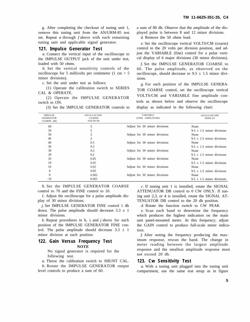
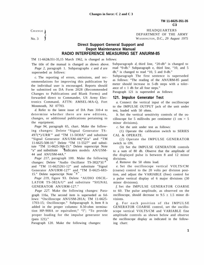
121. Impulse Generator Testa. Connect the vertical input of the oscilloscope to
the IMPULSE OUTPUT jack of the unit under test,loaded with 50 ohms.
b. Set the vertical sensitivity controls of theoscilloscope for 5 millivolts per centimeter (1 cm = 5minor divisions).
c. Set the unit under test as follows:(1) Operate the calibration switch to SERIES
CAL & OPERATE.(2) Operate the IMPULSE GENERATOR
switch to ON.(3) Set the IMPULSE GENERATOR controls to
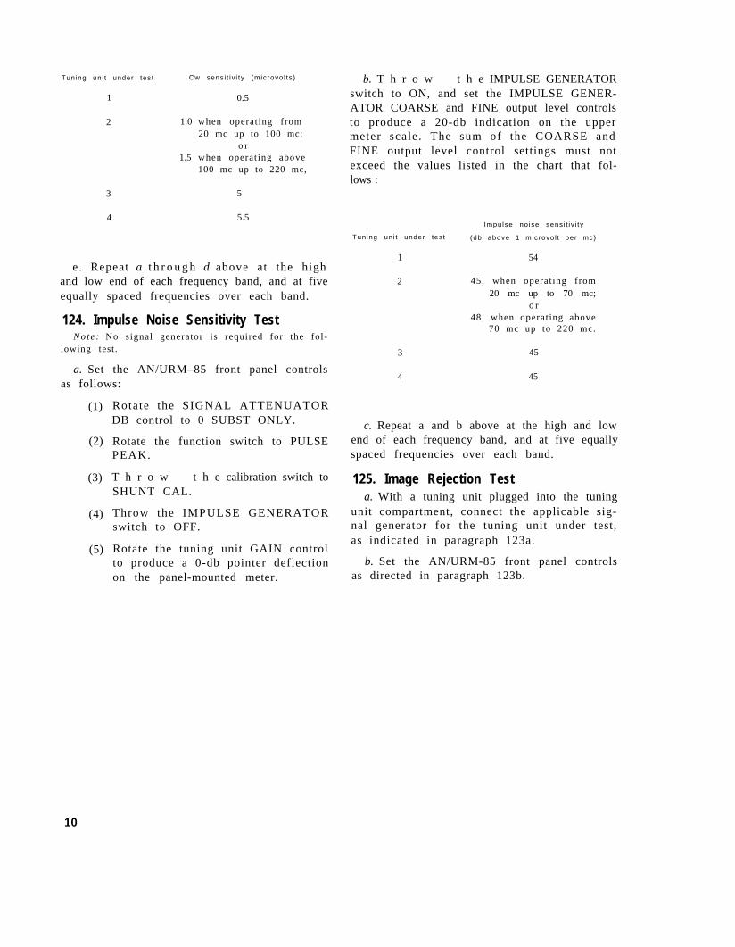
TM 11-6625-351-35, C4
a sum of 80 db. Observe that the amplitude of the dis-played pulse is between 8 and 12 minor divisions.
d. Remove the 50 ohms load.
e. Set the oscilloscope vertical VOLTS/CM (coarse)control to the 20 volts per division position, and ad-just the VARIABLE (fine) control for a pulse verti-cal display of 6 major divisions (30 minor divisions).
f. Set the IMPULSE GENERATOR COARSE to60. The pulse amplitude, as observed on theoscilloscope, should decrease to 9.5 ± 1.5 minor divi-sions.
g. For each position of the IMPULSE GENERA-
TOR COARSE control, set the oscilloscope vertical
VOLTS/CM and VARIABLE fine amplitude con-
trols as shown below and observe the oscilloscope
display as indicated in the following chart:
IMPULSE OSCILLSCOPE VARIABLE OSCILLOSCOPEGENERATOR COARSE (FINE AMPLITUDE)COARSE (db)
DISPLAYVOLTS/CM
605050404030302020101000
55220.50.50.20.20.050.050.020.020.005
Adjust for 30 minor divisions None9.5 ± 1.5 minor divisions
Adjust for 30 minor divisions None9.5 ± 1.5 minor divisions
Adjust for 30 minor divisions None9.5 ± 1.5 minor divisions
Adjust for 30 minor divisions None9.5 ± 1.5 minor divisions
Adjust for 30 minor divisions None9.5 ± 1.5 minor divisions
Adjust for 30 minor divisions None9.5 ± 1.5 minor divisions
Adjust for 30 minor divisions None-10 0.005 9.5 ± 1.5 minor divisions
h. Set the IMPULSE GENERATOR COARSEcontrol to 70 and the FINE control to 10.
i. Adjust the oscilloscope for a pulse amplitude dis-play of 30 minor divisions.
j. Set IMPULSE GENERATOR FINE control 1 dbdown. The pulse amplitude should decrease 3.3 ± 1minor divisions.
k. Repeat procedures in h, i, and j above for eachposition of the IMPULSE GENERATOR FINE con-trol. The pulse amplitude should decrease 3.3 ± 1minor division at each position.
122. Gain Versus Frequency TestNOTE
No signal generator is required for thefollowing test.
a. Throw the calibration switch to SHUNT CAL.b. Rotate the IMPULSE GENERATOR output
level controls to produce a sum of 60.
c. If tuning unit 1 is installed, rotate the SIGNALATTENUATOR DB control to 0 CW ONLY. If tun-ing unit 2,3, or 4 is installed, rotate the SIGNAL AT-TENUATOR DB control to the 20 db position.
d. Rotate the function switch to CW PEAKe. Scan each band to determine the frequency
which produces the highest indication on the mainunit panel-mounted meter. At this frequency, adjustthe GAIN control to produce full-scale meter indica-tion.
f. After noting the frequency producing the max-imum response, rescan the band. The change inmeter reading between the largest amplituderesponse and the smalleat amplitude response mustnot exceed 20 db.
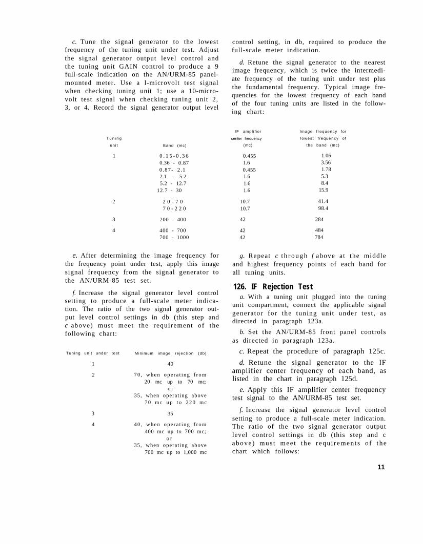
123. Cw Sensitivity Testa. With a tuning unit plugged into the tuning unit
compartment, use the same teat setup as in figure
5
TM 11-6625-351-35, C4
95.1, except for setting the variable step attenuator c. Adjust the signal generator level control to pro-to the 20 db position. Use the applicable signal vide a 10 microvolt signal at the SIGNAL INPUTgenerator (para 116) for the tuning unit under teat. jack if tuning unit 1 is installed or a 100 microvolt
b. Set the AN/URM-85 front panel controls as signal if tuning unit 2, 3, or 4 is installedfollows:
(1) If tuning unit 1 is installed rotate the SIG-d. Adjust the AN/URM-85 tuning unit GAIN con-
NAL ATTENUATOR DB control to 0 CW ONLY. Iftrol to produce a pointer deflection of 10 microvolt
tuning unit 2, 3, or 4 is installed, rotate the SIGNAL on the lower calibrated scale of the AN/URMS
ATTENUATOR DB control to the 20 db position. panel-mounted meter.
(2 ) Ro ta t e t he func t ion swi t ch t o CW e. Reduce the signal generator output level to zeroAVERAGE. and record the residual noise level indicated on the
(3) Throw the calibration switch to SERIES AN/URM-85 meter. This residual level must not ex-CAL & OPERATE. teed the values listed in the chart that follows:
Tuning unit under test Cw sensitivity (microvolts)
1 0.52 1.5 when operating from 20 MHz up to 100 MHz or 20 when operating above 100
MHz Up to 220 MHz34
f. Repeat a through e above at the low, middle, andhigh end of each band of each tuning unit.
124. Impulse Noise Sensitivity TestNOTE
No signal generator is required for thefollowing test.
a. Set the AN/URM-85 front panel controls asfollows:
(1) Rotate the SIGNAL ATTENUATOR DBcontrol to 0 SUBST ONLY.
(2) Rotate the function switch to PULSEP E A K
(3) Throw the calibration switch to SHUNTCAL.
Tuning unit under test
1234
c. Repeat a and b above at the low, middle, andhigh end of each band of each tuning unit.
125. Image Rejection Testa. With a tuning unit plugged into the tuning unit
compartment, connect the applicable signal genera-tor for the tuning unit under test, as indicated in
paragraph 123ab. Set the AN/URM-85 front panel controls as
directed paragraph 123b.c. Tune the signal generator to the lowest frequen-
cy of the tuning unit under test. Adjust the signal
6.07.0
(4) Throw the IMPUISE GENERATOR switchto OFF.
(5) Rotate the tuning unit GAIN control top-duce a 0-db pointer deflection on the panel-mounted
meter. If 0 db cannot be obtained, leave the GAIN
control fully clockwise.
b. Throw the IMPULSE GENERATOR switch to
ON, and set the IMPULSE GENERATOR COARSE
and FINE output level controls to produce a 20-db in-dication on the upper meter scale. The sum of the
COARSE and FINE output level control settingsmust not exceed the values listed in the chart that
follows:
Impulse noise sensitivity(db above 1 microvolt per MHz
60, for band 1, 54, for all other bands.505050
generator output level control and the tuning unit -
GAIN control to produce a full-scale indication onthe AN/URM-85 panel-mountd meter. Use a 10microvolt teat signal at the SIGNAL INPUT jackwhen checking tuning unit 1; use a 100-microvolttest signal when checking tuning unit 2, 3, or 4.Record the signal generator output level control set-ting, in db, required to produce the full-scale meterindication.
d. Retune the signal generator to the nearest im-
age frequency, which is twice the intermediate fre-
8
TM 11-6625-351-35, C4
quency of the tuning unit under test plus the funda-mental frequency. Typical image frequencies for the
TuningUnit (Hertz)
1 0.15 — 0.360.36 — 0.670.67 — 2.12.1 — 5.25.2 — 12.712.7 — 30
2 20 — 7070 — 220
3 200 — 00
4 400—700700 — 1000
e. After determining the image frequency for thefrequency point under test, apply this image signalfrequency from the s ignal generator to theAN/URM-85 test set.
f. Increase the signal generator level control set-
Tuning unit under test
lowest frequency of each band of the four tuningunits are listed in the following chart:
IF amplifiercenter frequency
(MHz)
0.4551.60.4551.61.61.6
Image frequency forlowest frequency of
the band (MHz)
1.063.561.785.38.4
15.9
10.7 41.410.7 91.4
42 284
42 48442 764
ting to produce a full-scale meter indication. Theratio of the two signal generator output level controlsettings in db (this step and c above) must meet therequirement of the following chart:
Minimum image rejection (db)
1 40, all bands except 6.35, band 6.2 65, when operating from 20 MHz up to 70 MHz or 30, when operating shove 70
MHz Up to 220 MHz3 304 35, when operating from 400 MHz up to 700 MHz or 30, when operating above 700
MHz Up to 1,000 MHz
g. Repeat c through f above at the middle andhighest frequency points of each band for all tuningunits.
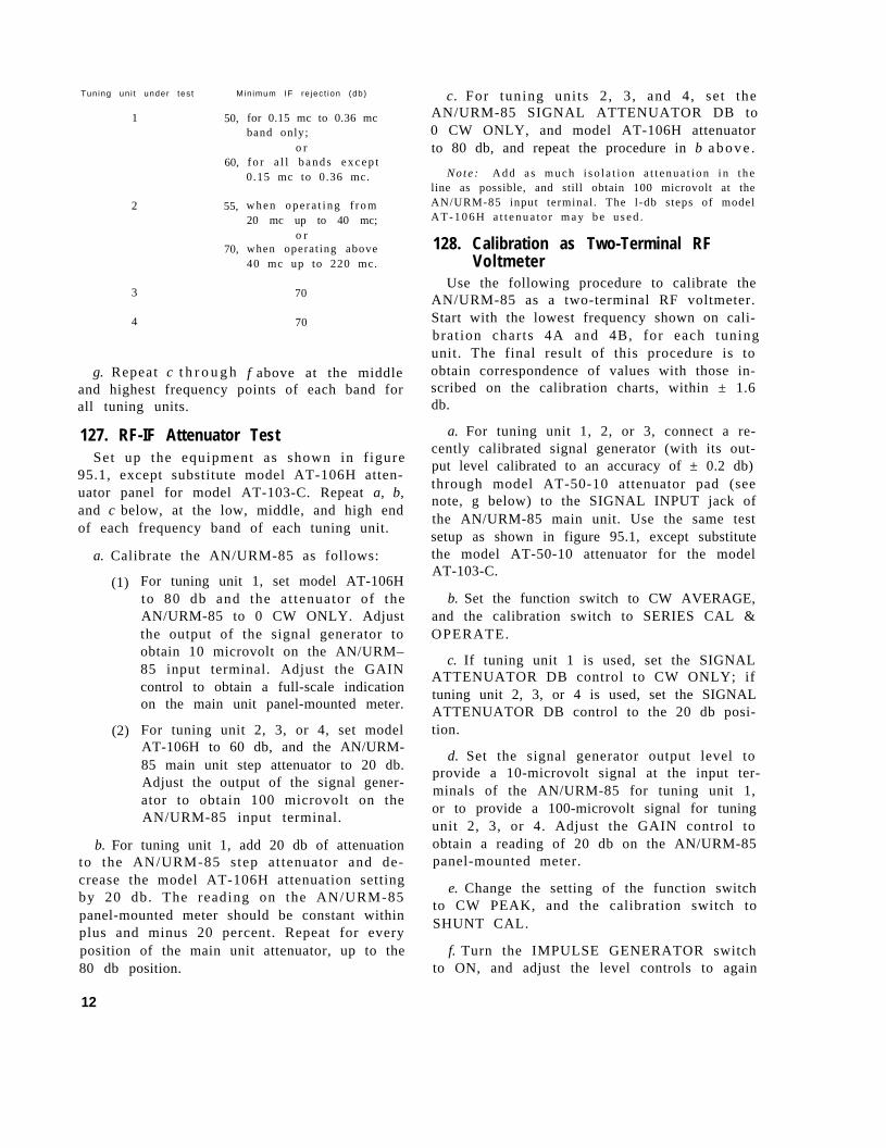
126. IF Rejection Testa With a tuning unit plugged into the tuning unit
compartment, connect the applicable signal genera-tor for the tuning unit under test, as directed in
paragraph 123a.b. Set the AN/URM-85 front panel controls as
directed in paragraph 123b.c. Repeat the procedure of paragraph 125c.
Tuning unit under test
d. Retune the signal generator to the IF amplifiercenter frequency of each band, as listed in the chart
in paragraph l25d.e. Apply this IF amplifier center frequency test
signal to the AN/URM-86 test set.
f. Increase the signal generator level control set-
ting to produce a full-scale meter indication. The
ratio of the two signal generator output level controIsettings in db (this step and c above) must meet therequirements of the chart which follows:
Minimum IF rejection (db)
1 45, for 03.15 MHz to 0.36 MHz band only or 55, ford bands except 0.15 MHz to 096MHz
2 55, when operating from 20 MHz up to 40 MHz or 60, when operating above 40MHz up to 220 MHz.
3 7 04 7 0
g. Repeat c through f above at the middle and high- 127. RF-IF Attenuator Testest frequency points of each band for all tuning Set up the equipment as shown in figure 95.1 exceptunits. substitute model AT-106H attenuator panel for
7
TM 11-6825-351-35, C4
model AT-103-C. Set the AN/URM-85 front panelcalibration switch to SERIES CAL & OPERATE,and the function switch to CW AVERAGE.
a. Calibrate the AN/URM-85 as follows:(1) Set model AT-106H to 80 db and the attena-
tor of the AN/URM-85 to 0 CW ONLY. Adjust theoutput of the s ignal generator to obtain 10microvolt on the AN/URM-85 input terminal. Ad-just the GAIN control to obtain a full-scale indica-tion on the main unit panel-mounted meter.
b. Add 20 db of attenuation to the AN/URM-85step attenuator and decrease the model AT-106H at-tenuation setting by 20 db. The reading on theAN/URM-835 panel-mounted meter should be cons-tant within plus and minus 4 db. Repeat for everyposition of the main unit attenuator, up to the 80-dbposition.
c. Repeat a and b above, at the low, middle, andhigh end of each frequency band of each tuning unit.
128. Ca l ibrat ion as Two-Terminal RFVoltmeterUse the following procedure to calibrate theAN/URM-85 as a two-terminal RF voltmeter. Startwith the lowest frequency shown on calibrationcharts 4A and 4B, for each tuning unit. The finalresult of this procdure is to obtain correspondenceof values with those inscribed on the calibrationcharts, within ± 1.6 db.
a. For tuning unit 1, 2, or 3, use the same testsetup as shown in figure 95.1 with the AT-103-C at-tenuator set to the 10-db position. All signal genera-tors used in this test shall have their output levelcalibrated to an accuracy of ± 0.2 db.
b. Set the function switch to CW AVERAGE, and
the calibration switch to SERIES CAL & OPER-ATE.
c. If tuning unit 1 is used, set the SIGNAL AT-TENUATOR DB control to CW ONLY; if tuningunit 2, 3, or 4 is used, set the SIGNAL ATTENUA-TOR DB control to the 20-db position.
d. Set the signal generator output level to providea 10-microvolt signal at the input terminals of theAN/URM-85 for tuning unit 1, or to provide a 100-microvolt signal for tuning unit 2,3, or 4. Adjust theGAIN control to obtain a reading of 20 db on theAN/URM-85 panel-mounted meter.
e. Change the setting of the function switch to CWPEAK and the calibration switch to SHUNT CAL.
f. Turn the IMPULSE GENERATOR switch toON, and adjust the level controls to again obtain a20-db reading on the main unit panel-mountedmeter . Record the set t ing of the IMPULSEGENERATOR level controls.
g. Repeat a through f above at every frequencyshown on calibration charts 4A and 4B, which aresupplied with each AN/URM-85 test set.
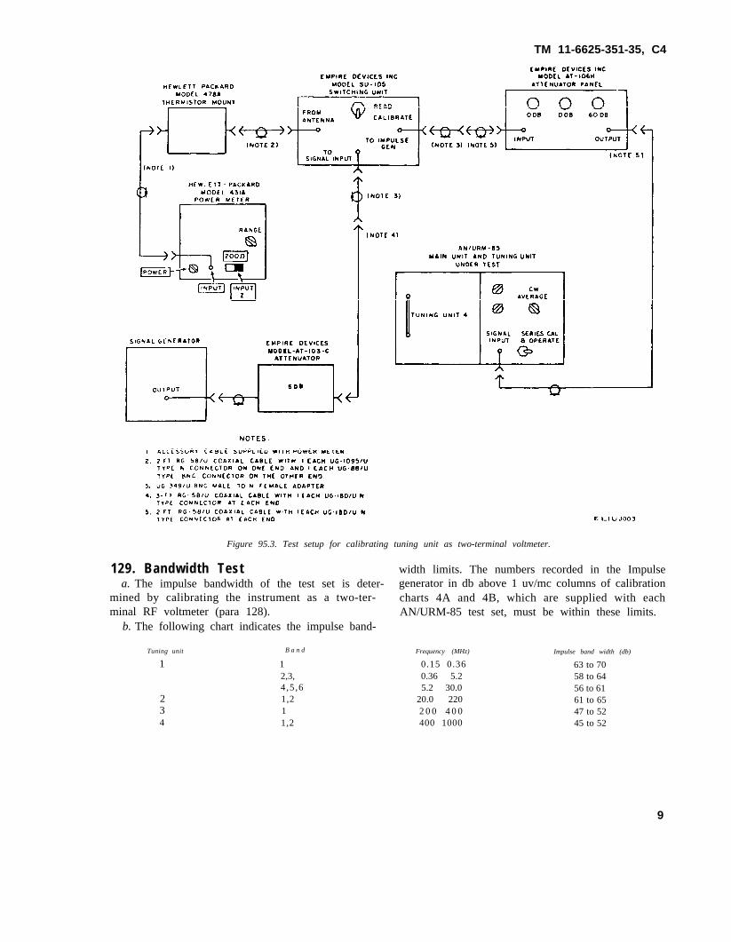
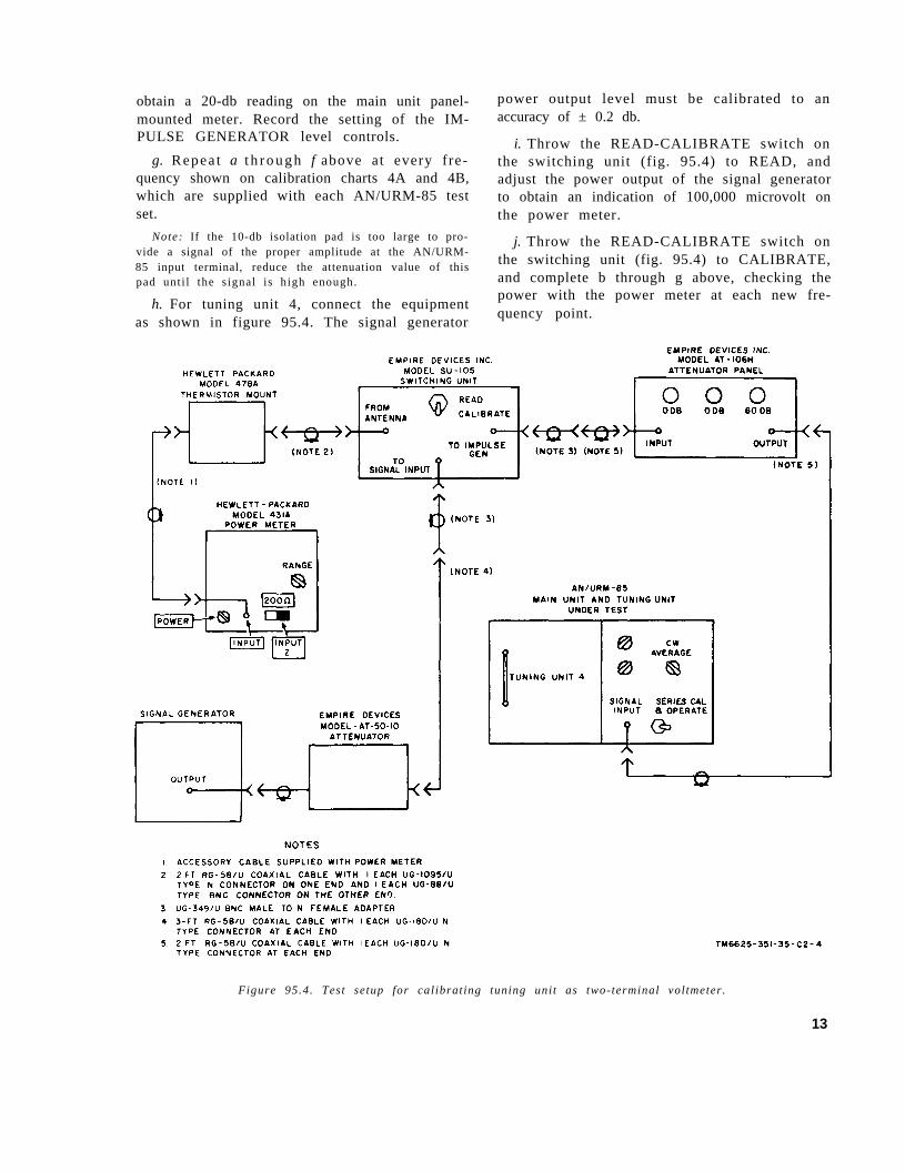
h. For tuning unit 4, connect the equipment asshown in figure 95.3. The power meter and thermis-or mount must be calibrated to an accuracy of ± 0.2db.
i. Throw the READ-CALIBRATE switch on theswitching unit (fig 95.3) to READ, and adjust thepower output of the signal generator to obtain an in-dication of 200 microwatts on the power meter.
j. Throw the READ-CALIBRATE switch on theswitching unit (fig 95.3) to CALIBRATE, and com-plete b through g above, checking the power with thepower meter at each new frequency point.
8
TM 11-6625-351-35, C4
Figure 95.3. Test setup for calibrating tuning unit as two-terminal voltmeter.
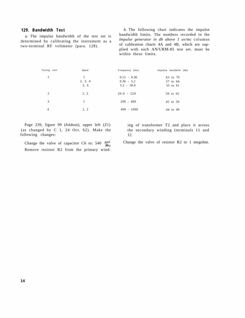
129. Bandwidth Test width limits. The numbers recorded in the Impulsea. The impulse bandwidth of the test set is deter-
mined by calibrating the instrument as a two-ter-minal RF voltmeter (para 128).
b. The following chart indicates the impulse band-
generator in db above 1 uv/mc columns of calibrationcharts 4A and 4B, which are supplied with eachAN/URM-85 test set, must be within these limits.
B a n d Frequency (MHz) Impulse band width (db)
0.15 0.36 63 to 700.36 5.2 58 to 645.2 30.0 56 to 61
20.0 220 61 to 652 0 0 4 0 0 47 to 52400 1000 45 to 52
Tuning unit
1 12,3,4 ,5 ,61,211,2
234
9
TM 11-6625-351-35, C4
By Order of the Secretary
Official:PAUL T. SMITH
of the Army:
FRED C. WEYANDGeneral, United States ArmyChief of Staff
Major General United States ArmyThe Adjutant General
Distribution:Active Army
USASA (2)COE (1)TSG (1)USMRENBD (1)DARCOM (1)TRADOC (2)OS Maj Cored (4)LOGCOMDS (3)MICOM (2)TECOM (2)USACC-CONUS (2)USACC-EUR (2)USACC-PAC (2)USACC-SO (2)USACC-T (2)USACC (4)MDW (1)Armies (2)corps (2)HISA (Ft Monmouth) (33)Svc Colleges (1)USASESS (5)USAADS (2)USAFAS (2)USAARMS (2)USAIS (2)USAES (2)USAICS (3)USACC-A (2)
MAAG (1)USARMIS (1)USAREUR (10)USAERDM (1)USAERDAW (1)Sig FLDMS (1)MAAG, Republic of china (2)installation (2) except
Fort Carson (5)Fort Gillem (10)Fort Gordon (10)Fort Huachuca (10)Ft Richardson (ECOM Ofc) (2)LBAD (14)SMD (30)TOAD (14)SHAD (3)
Units org under fol TOE: (1)11-1611-9711-9611-11711-30211-500(AA-AC)29-13429-13630-2530-29
NG: NoneUSAR: NoneFor explanation of abbreviations used see, AR 310-50
10
Changes in force: C 2 and C 3
TM 11-6625-351-35C3
CH A N G E HEADQUARTERSDEPARTMENT OF THE ARMY
No. 3 WASHINGTON , D.C., 29 August 1975
Direct Support General Support andDepot Maintenance Manual
RADIO INTERFERENCE MEASURING SET AN/URM-85TM 11-662&351-35,15 March 1962, is changed as follows:
The title of the manual is changed as shown above.Page 2, paragraph 1. Subparagraphs c and d are
superseded as follows:
c. The reporting of errors, omissions, and rec-ommendations for improving this publication bythe individual user is encouraged. Reports shouldbe submitted on DA Form 2028 (RecommendedChanges to Publications and Blank Forms) andforwarded direct to Commander, US Army Elec-tronics Command, ATTN: AMSEL-MA-Q, FortMonmouth, NJ 07703.
d. Refer to the latest issue of DA Pam 310-4 tode t e rmine whe the r t he r e a r e new ed i t i ons ,changes, or additional publications pertaining tothe equipment.
Page 94, paragraph 65, chart. Make the follow-ing changes: Delete “Signal Generator TS-497(*)/URR a” and “TM 11-5030A” and substitute“Signal Generator AN/USM-44(*)Ua” and “TM11-6625-508-10.” Delete “TM 11-5527” and substi-tute “TM 11-6625-366-15.” Delete superscript Note“a” and substitute Indicates models AN/USM-44 and AN/USM-44A.”
Page 217, paragraph 100. Make the followingchanges: Delete “Audio Oscillator TS-382(*)Uand “TM 11-6625261-12” and substitute "SignalGenerator AN/URM-127" and “TM ll-6625-683-15.” Delete superscript Note .
Page 219, figure 93. Delete “AUDIO OSCIL-LATOR TS-382A/U” and substitute “SIGNALGENERATOR AN/URM-127.”
Page 227. Make the following changes: Para-graph 116a, The second item is superseded as fol-lows: “Oscilloscope AN/USM-281A; TM 11-6625-1703-15; Oscilloscope.” Subparagraph b, Item 8 isadded in the proper columns: 8.50-ohm termina-tion HP-908A or equivalent;” “l”; “To provideproper loading for the impulse generator test(para 121).”Paragraph 120. Make the following changes:
Subparagraph d, third line, “20-db” is changed toread “0-db.” Subparagraph e, third line, “10, and 5db,” is changed to read “10, 5 and 0-db.”Subparagraph The first sentence is supersededas follows: “The reading of the AN/URM-85 panelmeter should increase in 5-db steps with a toler-ance of ± 1 db for all four steps.”Paragraph 121 is superseded as follows:
121. Impulse Generator Testa. Connect the vertical input of the oscilloscope
to the IMPULSE OUTPUT jack of the unit undertest, loaded with 50 ohms.
b. Set the vertical sensitivity controls of the os-cilloscope for 5 millivolts per centimeter (1 cm = 5minor divisions).
c. Set the unit under test as follows:(1) Operate the calibration switch to SERIES
CAL & OPERATE.(2) Operate the IMPULSE GENERATOR
switch to ON.(3) Set the IMPULSE GENERATOR controls
to a sum of 80 db. Observe that the amplitude ofthe displayed pulse is between 8 and 12 minordivisions.
d. Remove the 50 ohms load.e. Set the oscilloscope vertical VOLTS/CM
(coarse) control to the 20 volts per division posi-tion, and adjust the VARIABLE (free) control fora pulse vertical display of 6 major divisions (30minor divisions).
f. Set the IMPULSE GENERATOR COARSEto 60. The pulse amplitude, as observed on theoscilloscope, should decrease to 9.5 ± 1.5 minor di-visions.
g . F o r e a c h p o s i t i o n o f t h e I M P U L S EGENERATOR COARSE control, set the oscillo-scope vertical VOLTS/CM and VARIABLE fineamplitude controls as shown below and observethe oscilloscope display as indicated in the follow-ing chart:
1
“a
a ”
" a "
INPULSE GENERATOR OSCILLOSCOPE VARIABLE OSCILLOSCOPECOARSE (DB) COARSE VOLTS/CM (FINE AMPLITUDE) DISPLAY
605050404030302020101000-10
55220.50.50.20 20.050.050.020.020.0050.005
Adjust for 30 minor divisions---Adjust for 30 minor divisions---
Adjust for 30 minor divisions---
Adjust for 30 minor divisions---
Adjust for 30 minor divisions---
Adjust for 30 minor divisions---
Adjust for 30 minor divisions---
None9.5 ± 1.5 minor divisions
None9.5 ± 1.5 minor divisionsNone9.5 ± 1.5 minor divisionsNone9.5 ± 1.5 minor divisionsNone9.5 ± 1.5 minor divisionsNone9.5 ± 1.5 minor divisionsNone9.5 ± 1.5 minor divisions
h. Set the IMPULSE GENERATOR COARSEcontrol to 70 and the FINE control to 10.
i. Adjust the oscilloscope for a pulse amplitudedisplay of 30 minor divisions.
j. Set IMPULSE GENERATOR FINE control 1db down. The pulse amplitude should decrease 3.3± 1 minor divisions.
k. Repeat procedures in h, i, and j above for eachposition of the IMPULSE GENERATOR FINEcontrol. The pulse amplitude should decrease 3.3± 1 minor division at each position.Figure 95.3 is deleted.Paragraph 122c is superseded as follows:
c. If tuning unit 1 is installed, rotate the SIG
NAL ATTENUATOR DB control to 0 CW ONLY.If tuning unit 2, 3, or 4 is installed, rotate theSIGNAL ATTENUATOR DB control to the 20 dbposition.
Paragraph 123b(1) is superseded as follows:(1) If tuning unit 1 is installed, rotate the
SIGNAL ATTENUATOR DB control to 0 CWONLY. If tuning unit 2,3, or 4 is installed, rotatethe SIGNAL ATTENUATOR DB control to the20 db position.
Paragraph 124a(5). Add “If 0 db cannot be ob-tained, leave the GAIN control fully clockwise.”
Page 231. Appendix is superseded as follows:
APPENDIXREFERENCES
The following publications contain information applicable to the maintenance of Radio InterferenceMeasuring Set AN/URM-85.
DA Pam 310-4
DA Pam 310-7SB 11-573
SB 38-100
TB 43-0116TB 43-180TB 746-10
TM 11-1242
TB 11-5551-DTM 11-6625-200-15
Index of Technical Manuals, Technical Bulletins, Supply Manuals, (Types 7,8,and 9), Supply Bulletins and Lubrication Orders.
US Army Equipment Index of Modification Work Orders.Painting and Preservation Supplies Available for Field Use for Electronics
Command Equipment.Preservation, Packaging, Packing and Marking Materials, Supplies and
Equipment Used by the Army.Identification of radioactive items in the Army Supply System.Calibration Requirements for the Maintenance of Army Materiel.Field Instructions for Painting and Preserving Electronics Command
Equipment.Crystal Rectifier Test Sets TS-268/U, TS-268A/U, TS-268B/U, TS-268C/U, TS-
268D/U, and TS-268E/U.R.F. Signal Generator Set AN/URM-25D.Operator’s, Organizational, DS, GS, and Depot Maintenance Manual; Mul-
timeters ME-26A/U, ME-26B/U, ME-26C/U, and ME-26D/U.
2
TM 11-6625-274-12
TM 11-6625-280-15
TM 11-6625-320-12
TM 11-6625-351-12
TM 11-6625-351-20P
TM 11-6625-351-34P
TM 11-6625-366-15
TM 11-6625-508-10TM 11-6625-683-15
TM 11-6625-1703-15
TM 38-750TM 740-90-1TM 750-2442
Operator’s and Organizational Maintenance Manual: Test Sets, ElectronTube TV-7/U, TV-7A/U, TV-7B/U, and TV-7D/U.
Organizational, Field and Depot Maintenance Manual: Signal GeneratorsAN/URM-49, AN/URM-49A, AN/URM-49B, and AN/URM-49C.
Operator and Organizational Maintenance Manual: Voltmeter, Meter ME30A/U, and Voltmeters Electronic ME-30B/U, ME30C/U, and ME-30E/U.
Operator and Organizational Maintenance Manual: Radio InterferenceMeasuring Set AN/URM-85.
Organizational Maintenance Repair Parts and Special Tools Lists: RadioInterference Measuring Set AN/URM-85, FSN 6625-776-0595.
Direct Support and General Support Maintenance Repair Parts and SpecialTools List (Including Depot Maintenance Repair Parts and Special Tools):Radio Interference Measuring Set AN/URM-85, FSN 6625-776-0595.
Operator’s, Organizational, DS, GS, and Depot Maintenance Manual:Multimeter TS-352B/U.
Operator’s Manual: Signal Generators AN/USM-44 and AN/USM-44A.Operator, Organizational, Direct Support, General Support, and Depot
Maintenance Manual: Signal Generator AN/URM-127.Operator, Organization, DS, GS, and Depot Maintenance Manual Including
Repair Parts and Special Tool Lists: Oscilloscope AN/USM-281AThe Army Maintenance Management Systems (TAMMS).Administrative Storage of Equipment.Procedures for Destruction of Electronics Materiel to Prevent Enemy Use
(Electronics Command).
3

By Order of the Secretary of the Army:
Official:
VERNE L. BOWERSMajor General, United States ArmyThe Adjutint General
Distribution:Active Army:
USASA (2)Dir of Trans (1)COE (1)TSG (1)USAARENBD (1)AMC (1)MICOM (2)TECOM (2)TRADOC (2)ARADCOM (2)ARADCOM Rgn (2)OS Maj Comd (4) except
USAREUR (10)LOGCOMD (3)USACC (4)USACC-CONUS (2)USACC-EUR (2)USACC-PAC (2)USACC-L (2)USACC-SO (2)USASTRATCOM-T (2)MDW (1)Armies (2)Corps (2)HISA (Ft Monmouth) (43)Ft Gillem (10)Ft Gordon (10)Ft Huachua (10)Ft Carson (5)Ft Richardson (ECOM Ofc) (2)WSMR (1)Svc Colleges (1)USASESS (5)USAINTCS (3)USAADS (2)USAFAS (2)USAARMS (2)USAIS (2)USAES (2)USA Dep (2)
ARNG & USAR: None.For explanation of abbreviations used, see AR 310-50.
FRED C. WEYANDGeneral, United Statis ArmyChief of Staff
Sig Sec USA Dep (2)Sig Dep (2)AD (1) except
SAAD (30)LBAD (14)TOAD (14)SHAD (3)
ATS (1)MAAG (1)WRAMC (1)MAAG, Republic of China (2)USAERDAA (1)USAERDAW (1)USARMIS (1)Sig FLDMS (1)Units org under fol TOE: 1 ea.
11-1611-9711-9811-11711-500 (AA-AC)29-13429-13630-2530-2955-458
4
CHANGE
No. 1
Change now in force: C2TM 11-6625-351-35
*C2
HEADQUARTERSDEPARTMENT OF THE ARMY
Washington D. C., 10 October 1967
Field and Depot Maintenance Manual
RADIO INTERFERENCE MEASURING SET AN/URM-85
TM 11-6625-351-35, 15 March 1962, is changed as follows:Page 8. Delete figure 2 (as changed by C 1, 24 Oct. 62) and substitute new figure 2.
*This change supersedes C 1, 24 October 1962.
1
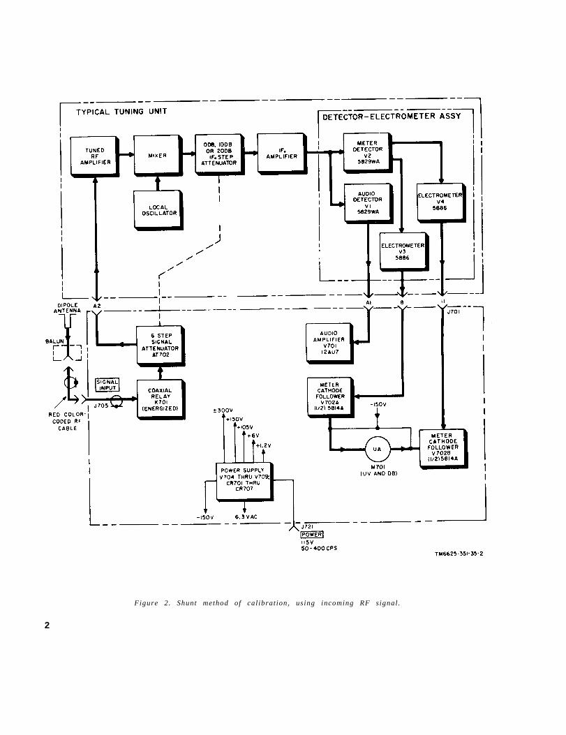
Figure 2. Shunt method of cal ibration, using incoming RF signal .
2
Page 38, figure 16 (upper left) (as changedby C 1, 24 Oct. 62). Make the following changes:
Change the value of capacitor C6 to: 540
Remove resistor R2 from the primary wind-ing of transformer T2 and place it acrossthe secondary winding (terminals 11 and12). Change the value of resistor R2 to:1 megohm.
Page 124, figure 58 (as changed by C 1, 24Oct. 62). Add the following note under Z1.
NOTE :THE POSITION OF RESISTOR R2 HAS BEENCHANGED SO THAT IT IS CONNECTED ACROSSTHE SECONDARY WINDING OF TRANSFORMERT2 (TERMINALS 11 AND 12).
Page 227. After chapter 4, add chapter 5.
CHAPTER 5
DEPOT OVERHAUL STANDARDS
114. Applicability of Depot OverhaulStandards
The tests outl ined in this chapter are de-signed to measure the performance capabilityof a repaired electronic equipment. Equipmentthat is to be returned to stock should meet thestandards given in these tests.
115. Applicable Referencesa. Repair Standards. Applicable procedures
of the depots performing these tests and thegeneral standards for repaired electronic equip-
ment given in TB SIG 355-1, TB SIG 355-2,and TB SIG 355-3 form a part of the require-ments for testing this equipment.
b. Technical Publicat ions. The only othertechnical publication applicable to the equip-ments to be tested is TM 11-6625-251-12.
c. Modification Work Orders. Perform al lmodif icat ion work orders appl icable to thisequipment before making the tests specified.DA Pam 310-7 lists all available MWO’s.
3
116. Test Facilities RequiredThe following items are needed for depot
testing:
a. Test Equipment.
I tem Technical Manual
Generator, Signal AN/URM-127 TM 11-6625-683-15
Generator, Pulse SG-128/U
Multimeter TS-352B/U TM 11-6625-366-15
G e n e r a t o r , S i g n a l A N / U R M - 2 5 F TM 11-5551-E
G e n e r a t o r , S i g n a l A N / U R M - 4 9 TM 11-6625-280-15
Generator, Signal AN/USM-44 TM 11-6625-508-10
Voltmeter, Electronic ME-30C/U TM 11-6625-320-12
b. Additional Equipment.
E q u i p m e n t Quant i ty Req’d.
1. Empire Devices Inc. Model 1AT-103-C step at tenuator(variable in 5-db steps from0 to 25 db).
2. Empire Devices Inc. ModelAT-50-10 coaxial at tenuator.
3. Empire Devices Inc. ModelAT-50-20 coaxial at tenuator.
4. Empire Devices Inc. ModelAT-106H microwaveattenuator panel.
5. Empire Devices Inc. ModelSU-105 switching unit .
6 . H e w l e t t - P a c k a r d M o d e l 4 3 1 Bpower meter.
7 . H e w l e t t - P a c k a r d M o d e l 4 7 8 At h e r m i s t o r m o u n t ,
1
1
1
5
1
1
C o m m o n N a m e
Signal generator.
Pulse generator.
Mul t ime te r .
Voltmeter, electronic.
Appl icat ion
Used in linearity test (para. 120), as am e a n s o f a t t e n u a t i n g t h e i n p u t t e s tsignal to the test set , in 5-db steps.
U s e d a s a n i s o l a t i o n p a d f o r t h e s i g n a lgenerator.
U s e d a s a n i s o l a t i o n p a d f o r t h e s i g n a lgenerator.
U s e d i n t h e t w o - t e r m i n a l R F v o l t m e t e rcalibrat ion test as a means of at tenuat-ing the input test s ignal to the test setin 20-db steps.
U s e d i n t h e t w o - t e r m i n a l R F v o l t m e t e rcalibrat ion test as a means of switch-i n g f r o m t h e p o w e r m e t e r t o t h e t e s tset in use.
Used to monitor power for cal ibrat ion asa two-terminal RF voltmeter (f ig, 95.4).
Used to monitor power for cal ibrat ion asa two-terminal RF voltmeter (f ig. 95.4).
4
117. General Requirements 118. Dial Calibration Accuracy TestThe following tests shall be performed. In- a. With a tuning unit plugged into the main
put power shall be 115 volts, 60 cps, single unit compartment, connect a cable from the rfphase. The results shall be as specified in each output jack on the appropriate signal generator,test. for the frequency under test, to the SIGNAL
INPUT jack on the AN/URM-85 main unit(fig. 95.1 ). Set the variable attenuator to the20-db position.
Figure 95.1. Test setup for dial cal ibration accuracy and l ineari ty test .
5
b. Initially, set the front panel controls asdescribed below:
Tuning Uni t
In Use
1
Control
MEGACYCLES band switch
Sett ing
First set to 0.15-0.36: then to each ofthe r ema in ing f i ve bands a f t e r asat isfactory performance indicat ionin the previous band has been ob-served.
FREQUENCY-RANGE-MCswitch
First set to 20-70 MC band; then setto 70-220 MC band after a satisfac-tory indication in the 20-70 MC bandhas been observed.
Note: This tuning unit doesnot employ band switching.
Not applicable.3
4 F i r s t s e t t o 400 -700 MC band ; t hense t t o 700 -1 ,000 MC band a f t e r asat isfactory performance indicat ionin the 400-700 MC band has been ob-served.
F R E Q U E N C Y R A N G Eswitch
Tuning Uni t
In Use Control Set t ing
CW AVERAGE.Function switch1,
2,
3,
S IGNAL ATTENUATOR DBcontrol
20.
SERIES CAL & OPERATE:
O F F .
o r
4
Calibration switch
I M P U L S E - G E N E R A T O RON-OFF swi t ch .
GAIN control Midposition.
Set for comfortable level of audio sig-nal, if aural monitoring of input sig-nal is employed.
VOLUME control
O NPOWER ON-OFF swi tch
c. Set the function switch to CW AVERAGE. ator to obtain an on-scale reading on the panel-
d. Set the band swtich (if applicable) and themounted meter of the main unit.
TUNING control to the lowest band and tuning f. Adjust the TUNING control on the tuningdial frequency setting. Tune the signal gener- u n i t t o o b t a i n t h e m a x i m u m r e a d i n g o nator to the same frequency. meter. If necessary, adjust the at teuator on
the signal generator to keep the reading on-e. Adjust the attenuator on the signal gener- scale.
6
g. Read the f requency on the tuning uni tdial. This reading must be within 2 percent ofthe known accurately calibrated signal gener-ator frequency.
h. Repeat d through g above, increasing thesignal generator frequency in steps of 10 mc.
i. Repeat a through h above with a differ-ent tuning unit installed in the main unit. Startat the lowest frequency setting, and increase
both the signal generator frequency output andthe tuning unit frequency dial in 10-mc incre-ments. For each tuning unit, the frequency dialaccuracy must be within 2 percent of the sig-nal generator frequency.
119. Audio Amplifier Response TestTo check the response of audio amplifier
V701 in the main unit, set up the equipmentas shown in figure 95.2, and proceed as follows:
Figure 95.2. Test setup for
a. Connect the output of the signal generator(para. 116) to the input of audio amplifierV701A in the main unit of the AN/URM-85test set. A convenient point for injecting thesignal generator signal is at the unnumberedfeedthrough terminal at the bottom right cor-ner of the filter box assembly. The filter boxassembly is accessible at the rear of the mainunit of the AN/URM–85 test set. This terminalis essentially the same circuit point as terminalAl of connector J701.
b. Connect Voltmeter, Electronic ME-30C/U
audio ampli f ier response test .
across a 600-ohm, ½-watt resistor tied fromPHONES jack J702 to chassis ground.
c. Adjust the output of the signal generatorto produce a signal of 0.1-volt amplitude fromterminal A1 of J701 (fig. 95.2) to ground.
d. Tune the signal generator to 1,000 cpsand record the voltage indication shown onVoltmeter, Electronic ME-30C/U.
e. Repeat d above at test frequencies of 150;500; 2,000; 3,000; 4,000; and 5,000 cps respec-tively. Note the voltage reading at each testfrequency. The audio response curve must be
7
flat, within 8 db, of the 1,000-cycle value, witha gradual slope-off at each end. There can beno resonant peaks.
120. linearity TestTo check the linearity of the AN/URM-85
test set , set up the equipment as shown infigure 95.1 and proceed as follows:
a. Se t t he AN/URM-85 t e s t s e t f unc t ionswitch to PULSE PEAK.
b. Set the Model AT-103-C step attenuatorto its 20-db position.
c. Set the signal generator output level con-trol to produce a 1,000-microvolt signal at theSIGNAL INPUT jack.
d. Rotate the SIGNAL ATTENUATOR DBcontrol to 60 and adjust the GAIN control onthe tuning unit to produce a 20-db indicationon the AN/URM–85 test set panel-mountedmeter.
e. Change the setting of the variable stepattenuator in four 5-db steps, from 20 to 15,10, and 5 db, and record the corresponding in-dication of the AN/URM-85 test set panel-mounted meter.
f. Correspondence between the external vari-able step attenuator and the AN/URM-85 metermust be within ± 1 db at all four steps. If theproper limits cannot be obtained, change theinput signal to a 10,000-microvolt level andrepeat d and e above.
g. After completing the checkout of tuningu n i t 1 , r e m o v e t h i s t u n i n g u n i t f r o m t h eAN/URM-85 test set. Repeat a through f a b o v ewith each remaining tuning unit and applicablesignal generator.
121. Interference Measurement TestTo perform this test, set up the equipment
as shown in figure 95.3 and proceed as follows:
a. Connect the IMPULSE OUTPUT jack ofthe pulse generator, through the 20-db pad, tothe SIGNAL INPUT jack of the AN/URM-85under test.
b. Set Generator Pulse, SG-128/U as follows:
(1) Throw the PULSE POLARITY switchto PLUS.
(2)
c. S e t
(1)
(2)
(3)
(4)
(5)
Set G e n e r a t o r Pulse, SG-128/UCOARSE and FINE output level con-trols to a value 20 db greater thanthe settings s h o w n on calibrationcharts 4A and 4B, supplied with theunit under test. This chart is suppliedwith each AN/URM-85 test set. Forinstance, if the calibration chart showsa value of 62 db, set Generator Pulse,SG-128/U COARSE and FINE con-trols to 82 db.
the unit under test as follows:
Rotate the function switch to CWPEAK.
T h r o w t h e calibration switch toSERIES CAL & OPERATE.
If tuning uni t 1 is instal led in theAN/URM-85 test set, rotate the SIG-NAL ATTENUATOR DB control to 0CW ONLY.
If tuning unit 2, 3, or 4 is installedin the AN/URM–85 test set, rotate theSIGNAL ATTENUATOR DB controlto the 20 position.
With the test set as indicated in figure95.3, record the pointer deflection onthe AN/URM-85 test set panel-mount-ed meter.
d. Throw the POWER switch on GeneratorPulse, SG-128/U to OFF.
e. O n
(1)
(2)
(3)
the unit under test:
T h r o w t h e calibration switch toSHUNT CAL.
Throw the IMPULSE GENERATORswitch to ON.
S e t t h e IMPULSE GENERATORCOARSE and FINE controls to thosesettings which produce the same point-er deflection on the main unit panel-mounted meter as were obtained inc ( 5 ) a b o v e . T h e s e t t i n g s o f t h eAN/URM-85 IMPULSE GENERA-TOR output controls must correspondwithin ± 1 db of the numbers shownon the calibration charts.
8
Figure 95.3. Test set up for interference measurement.
122. Gain Versus Frequency TestNote: No signal generator is required for the fol-
lowing test:
a. Throw the calibration switch to SHUNTCAL.
b. Rotate the IMPULSE GENERATOR out-put level controls to produce a sum of 60.
c. Rotate the SIGNAL ATTENUATOR DBcontrol to 20.
d. Rotate the function switch to CW PEAK.
e. Scan each band t o de t e rmine t he f r e -quency which produces the highest indicationon the main unit panel-mounted meter. At thisfrequency, adjust the GAIN control to producefull-scale meter indication.
f. After noting the frequency producing themaximum response, r es c a n the band. Thechange in meter reading between the largestamplitude response and the smallest amplituderesponse must not exceed 20 db.
123. Cw Sensitivity Testa. With a tuning unit plugged into the tun-
ing unit compartment, use the same test setup
as in figure 95.1, except for setting the variablestep attenuator to the 10 db position. Use theapplicable signal generator (para. 116) for thetuning unit under test.
b. Set the AN/URM-85 front panel controlsas follows:
(1) Rotate the SIGNAL ATTENUATORDB control to 0 CW ONLY.
(2) Rotate the function switch to CWAVERAGE.
(3) T h r o w t h e calibration switch toSERIES CAL & OPERATE.
c. Adjust the signal generator level controland the AN/URM–85 tuning unit GAIN con-trol to produce a pointer deflection of 10 mic-rovol t on the lower cal ibrated scale of theAN/URM-85 panel-mounted meter.
d. Reduce the signal generator output levelto zero, and record the residual noise level in-dicated on the AN/URM-85 meter. This re-sidual level must not exceed the values listedin the chart that follows:
9
Tuning un i t under test Cw sens i t iv i ty (microvo l ts )
1
2 1.0
1.5
3
4
0.5
when operating from20 mc up to 100 mc;
o rwhen operat ing above100 mc up to 220 mc,
5
5.5
e. Repeat a t h r o u g h d above at the highand low end of each frequency band, and at fiveequally spaced frequencies over each band.
124. Impulse Noise Sensitivity TestN o t e : No signal generator is required for the fol-
lowing test.
a. Set the AN/URM–85 front panel controlsas follows:
(1)
(2)
(3)
(4)
(5)
Rotate the SIGNAL ATTENUATORDB control to 0 SUBST ONLY.
Rotate the function switch to PULSEPEAK.
T h r o w t h e calibration switch toSHUNT CAL.
Throw the IMPULSE GENERATORswitch to OFF.
Rotate the tuning unit GAIN controlto produce a 0-db pointer deflectionon the panel-mounted meter.
b. T h r o w t h e IMPULSE GENERATORswitch to ON, and set the IMPULSE GENER-ATOR COARSE and FINE output level controlsto produce a 20-db indication on the uppermeter scale. The sum of the COARSE andFINE output level control settings must notexceed the values listed in the chart that fol-lows :
Impulse no ise sens i t iv i ty
Tuning un i t under test (db above 1 microvo l t per mc)
1 54
2 45, when operat ing from20 mc up to 70 mc;
o r48, when operat ing above
70 mc up to 220 mc.
3 45
4 45
c. Repeat a and b above at the high and lowend of each frequency band, and at five equallyspaced frequencies over each band.
125. Image Rejection Testa. With a tuning unit plugged into the tuning
unit compartment, connect the applicable sig-nal generator for the tuning unit under test,as indicated in paragraph 123a.
b. Set the AN/URM-85 front panel controlsas directed in paragraph 123b.
10
c. Tune the signal generator to the lowest control setting, in db, required to produce thefrequency of the tuning unit under test. Adjust full-scale meter indication.the signal generator output level control andthe tuning unit GAIN control to produce a 9full-scale indication on the AN/URM-85 panel-mounted meter. Use a l-microvolt test signalwhen checking tuning unit 1; use a 10-micro-volt test signal when checking tuning unit 2,3, or 4. Record the signal generator output level
d. Retune the signal generator to the nearestimage frequency, which is twice the intermedi-ate frequency of the tuning unit under test plusthe fundamental frequency. Typical image fre-quencies for the lowest frequency of each bandof the four tuning units are listed in the follow-ing chart:
T u n i n g
un i t
1
IF ampl i f ier Image f requency for
center frequency lowest f requency of
Band (mc) (mc) the band (mc)
0 . 1 5 - 0 . 3 6 0.455 1.060.36 - 0.87 1.6 3.560 .87- 2 .1 0.455 1.782.1 - 5.2 1.6 5.35.2 - 12.7 1.6 8.4
12.7 - 30 1.6 15.9
2 2 0 - 7 0 10.7 41.47 0 - 2 2 0 10.7 98.4
3 200 - 400 42 284
4 400 - 700 42 484700 - 1000 42 784
e. After determining the image frequency forthe frequency point under test, apply this imagesignal frequency from the signal generator tothe AN/URM-85 test set.
f. Increase the signal generator level controlsetting to produce a full-scale meter indica-tion. The ratio of the two signal generator out-put level control settings in db (this step andc above) must meet the requirement of thefollowing chart:
g. Repeat c t h r o u g h f above at the middleand highest frequency points of each band forall tuning units.
126. IF Rejection Testa. With a tuning unit plugged into the tuning
unit compartment, connect the applicable signalgenerator for the tuning uni t under tes t , asdirected in paragraph 123a.
b. Set the AN/URM-85 front panel controlsas directed in paragraph 123a.
Tuning un i t under test Min imum image re ject ion (db) c. Repeat the procedure of paragraph 125c.
1 40 d. Retune the signal generator to the IF
2 70 , when ope ra t i ng f romamplifier center frequency of each band, as
20 mc up to 70 mc; listed in the chart in paragraph 125d.o r e. Apply this IF amplifier center frequency
35, when operat ing above test signal to the AN/URM-85 test set.7 0 m c u p t o 2 2 0 m c
3 35f. Increase the signal generator level control
setting to produce a full-scale meter indication.4 40 , when ope ra t i ng f rom The ratio of the two signal generator output
400 mc up to 700 mc;level control settings in db (this step and c
o r35, when operat ing above above ) mus t mee t t he r equ i r emen t s o f t he
700 mc up to 1,000 mc chart which follows:
11
Tuning un i t under test Min imum IF re jec t ion (db)
1 50,
60,
2 55,
70,
3
4
g. Repeat c t h r o u g h
for 0.15 mc to 0.36 mcband only;
o rf o r a l l b a n d s e x c e p t0.15 mc to 0.36 mc.
when ope ra t i ng f rom20 mc up to 40 mc;
o rwhen operat ing above40 mc up to 220 mc.
70
70
f above at the middleand highest frequency points of each band forall tuning units.
127. RF-IF Attenuator TestSet up the equipment as shown in f igure
95.1, except substitute model AT-106H atten-uator panel for model AT-103-C. Repeat a, b,and c below, at the low, middle, and high endof each frequency band of each tuning unit.
a. Calibrate the AN/URM-85 as follows:
(1)
(2)
For tuning unit 1, set model AT-106Hto 80 db and the a t tenuator of theAN/URM-85 to 0 CW ONLY. Adjustthe output of the signal generator toobtain 10 microvolt on the AN/URM–85 input terminal. Adjust the GAINcontrol to obtain a full-scale indicationon the main unit panel-mounted meter.
For tuning unit 2, 3, or 4, set modelAT-106H to 60 db, and the AN/URM-85 main unit step attenuator to 20 db.Adjust the output of the signal gener-ator to obtain 100 microvolt on theAN/URM-85 input terminal.
b. For tuning unit 1, add 20 db of attenuationto the AN/URM-85 step at tenuator and de-crease the model AT-106H attenuation settingby 20 db. The reading on the AN/URM-85panel-mounted meter should be constant withinplus and minus 20 percent. Repeat for everyposition of the main unit attenuator, up to the80 db position.
12
c. For tuning uni ts 2 , 3 , and 4, se t theAN/URM-85 SIGNAL ATTENUATOR DB to0 CW ONLY, and model AT-106H attenuatorto 80 db, and repeat the procedure in b a b o v e .
N o t e : Add a s much i so l a t i on a t t enua t i on i n t heline as possible, and still obtain 100 microvolt at theAN/URM-85 input terminal . The l-db steps of modelA T - 1 0 6 H a t t e n u a t o r m a y b e u s e d .
128. Calibration as Two-Terminal RFVoltmeter
Use the following procedure to calibrate theAN/URM-85 as a two-terminal RF voltmeter.Start with the lowest frequency shown on cali-brat ion charts 4A and 4B, for each tuningunit. The final result of this procedure is toobtain correspondence of values with those in-scribed on the calibration charts, within ± 1.6db.
a. For tuning unit 1, 2, or 3, connect a re-cently calibrated signal generator (with its out-put level calibrated to an accuracy of ± 0.2 db)through model AT-50-10 attenuator pad (seenote, g below) to the SIGNAL INPUT jack ofthe AN/URM-85 main unit. Use the same testsetup as shown in figure 95.1, except substitutethe model AT-50-10 attenuator for the modelAT-103-C.
b. Set the function switch to CW AVERAGE,and the calibration switch to SERIES CAL &OPERATE.
c. If tuning unit 1 is used, set the SIGNALATTENUATOR DB control to CW ONLY; iftuning unit 2, 3, or 4 is used, set the SIGNALATTENUATOR DB control to the 20 db posi-tion.
d. Set the signal generator output level toprovide a 10-microvolt signal at the input ter-minals of the AN/URM-85 for tuning unit 1,or to provide a 100-microvolt signal for tuningunit 2, 3, or 4. Adjust the GAIN control toobtain a reading of 20 db on the AN/URM-85panel-mounted meter.
e. Change the setting of the function switchto CW PEAK, and the calibration switch toSHUNT CAL.
f. Turn the IMPULSE GENERATOR switchto ON, and adjust the level controls to again
obtain a 20-db reading on the main unit panel-mounted meter. Record the setting of the IM-PULSE GENERATOR level controls.
g. Repea t a t h r o u g h f above at every fre-quency shown on calibration charts 4A and 4B,which are supplied with each AN/URM-85 testset.
Note: If the 10-db isolation pad is too large to pro-vide a signal of the proper amplitude at the AN/URM-85 input terminal, reduce the attenuation value of thispad unti l the signal is high enough.
power output level must be calibrated to anaccuracy of ± 0.2 db.
i. Throw the READ-CALIBRATE switch onthe switching unit (fig. 95.4) to READ, andadjust the power output of the signal generatorto obtain an indication of 100,000 microvolt onthe power meter.
j. Throw the READ-CALIBRATE switch onthe switching unit (fig. 95.4) to CALIBRATE,and complete b through g above, checking the
h. For tuning unit 4, connect the equipmentpower with the power meter at each new fre-
as shown in figure 95.4. The signal generatorquency point.
Figure 95.4. Test setup for calibrating tuning unit as two-terminal voltmeter.
13
129. Bandwidth Test b. The following chart indicates the impulsebandwidth limits. The numbers recorded in thea. The impulse bandwidth of the test set is
determined by calibrating the instrument as a Impulse generator in db above 1 uv/mc columns
two-terminal RF voltmeter (para. 128). of calibration charts 4A and 4B, which are sup-plied with each AN/URM-85 test set. must bewithin these limits.
Tuning uni t Band Frequency (me) Impulse bandwi th (db)
1 1 0.15 - 0.36 63 to 702, 3, 4 0.36 - 5.2 57 to 64
5, 6 5.2 - 30.0 55 to 61
2 1, 2 20 .0 - 220 59 to 65
3 1 200 - 400 45 to 50
4 1, 2 400 - 1000 44 to 49
Page 239, figure 99 (foldout), upper left (Z1) ing of transformer T2 and place it across(as changed by C 1, 24 Oct. 62). Make the the secondary winding (terminals 11 andfollowing changes: 12.
Change the valve of capacitor C6 to: 540 Change the valve of resistor R2 to 1 megohm.
Remove resistor R2 from the primary wind-
14
By Order of the Secretary of the Army:HAROLD K. JOHNSON,General, United States Army,
Official: Chief of Staff.
KENNETH G. WICKHAM,Major General, United States Army,The Adjutant General.
Distribution:
USASA (2)CNGB (1)OCC-E (7)Dir of Trans (1)CofEngrs (1)TSG (1)Cofspts (1)USAARENBD (2)USAAVNTBD (5)USACDC Agcy (1)USAMC (5)USCONARC (5)ARADCOM (5)ARADCOM Rgn (2)OS Maj Comd (4)USARYIS (5)LOGCOMD ( 2 )USAMICOM (4)USASTRATCOM (4)USAESC (70)USASTRATCOM-EUR (8)UTSASTRATCOM-SO (8)USACOMZEUR (5)USASA (Pac) (5)USASA (Eur) (5)MDW (1)Armies (2) except
First USA (8)Fourth USA (8)
Corps (2)USAC (3)
12th USASA Fld Sta (5)1st Cav Div (5)Svc Colleges (2)USAADS (2)USAAMS (2)USAARMS (2)USAIS (2)USAES (2)USASESS (10)USATC Armor (2)USATCFLW (2)USATC Inf (2)USASTC (2)WRAMC (1)Army Pic Cen (2)USACDCEC (10)USAINTC (5)USAJFKCENSPWAR (5)ARADMAC (5)Instl (2) except
Fort Gordon (10)Fort Huachuca (10)Fort Carson (21)Fort Knox (12)Fort Belvoir (5)WSMR (5)APG (5)JCA, Fort Ritchie (5)
Army Dep (2) exceptLBAD (14)SAAD (30)
TOAD (14)LEAD (7)SHAD (3)NAAD (5)SVAD (5)CHAD (3)ATAD (10)
GENDEPS (2)Sig Sec GENDEPS (5)Sig Dep (12)Sig FLDMS (2)AMS (1)USAERDAA (2)USAERDAW (13)USACRREL (2)MAAG (2)USARMIS (2)USARMA (2)Units org under fol TOE:
( 2 copies each)11-5711-9711-9811-11711-12711-15511-15711-15811-500 (AA-AC)11-58711-59211-597
NG: None
USAR: None
For explanation of abbreviations used, see AR 320-50.
15

TM 11-6625-351-35
Technical Manual HEADQUARTERS,DEPARTMENT OF THE ARMY
No. 11-6625-351-35 WASHINGTON 25, D. C., 15 March 1962
RADIO INTERFERENCE MEASURING SET AN/URM-85
C H A P T E R 1 .S e c t i o n I .
II.III.IV.V.
VI.VII.
C H A P T E R 2 .S e c t i o n I .
I IC H A P T E R 3 .
S e c t i o n I .II.
C H A P T E R 4 .APPENDIX
ParagraphTHEORYSystem block diagram 1 - 7Theory of main unit 8 - 2 4Theory of tuning unit l 25-33Theory of tuning unit 2 34-41Theory of tuning unit 3 42-49Theory of tuning unit 4 50-58Theory of minor components 59-62TROUBLESHOOTINGGeneral troubleshooting techniques 63-65Troubleshooting test set 66-75REPAIRS AND ALIGNMENTR e p a i r s 7 6 - 8 0A l i g n m e n t 8 1 - 9 8FINAL TESTINGREFERENCES
99-113
INDEX
Page
2—1011—3335—4747—5858—6969—8181—89
91—93106—164
166—188190—213217—227
231232
1
CHAPTER 1
THEORY
Section I. SYSTEM BLOCK DIAGRAM
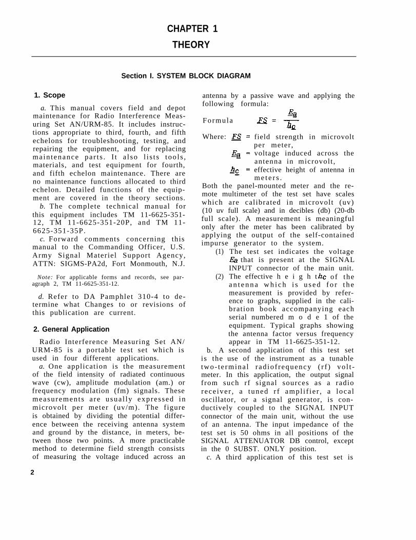
1. Scope
a. This manual covers field and depotmaintenance for Radio Interference Meas-uring Set AN/URM-85. It includes instruc-tions appropriate to third, fourth, and fifthechelons for troubleshooting, testing, andrepairing the equipment, and for replacingmain tenance pa r t s . I t a l so l i s t s t oo l s ,materials, and test equipment for fourth,and fifth echelon maintenance. There areno maintenance functions allocated to thirdechelon. Detailed functions of the equip-ment are covered in the theory sections.
b. The complete technical manual forthis equipment includes TM 11-6625-351-12, TM 11-6625-351-20P, and TM 11-6625-351-35P.
c. Forward comments concerning thismanual to the Commanding Officer, U.S.Army Signal Materiel Support Agency,ATTN: SIGMS-PA2d, Fort Monmouth, N.J.
Note: For applicable forms and records, see par-agraph 2, TM 11-6625-351-12.
d. Refer to DA Pamphlet 310-4 to de-termine what Changes to or revisions ofthis publication are current.
2. General Application
Radio Interference Measuring Set AN/URM-85 is a portable test set which isused in four different applications.
a. One application is the measurementof the field intensity of radiated continuouswave (cw), amplitude modulation (am.) orfrequency modulation (fm) signals. Thesemeasurements a re usua l ly expressed inmicrovolt per meter (uv/m). The f igureis obtained by dividing the potential differ-ence between the receiving antenna systemand ground by the distance, in meters, be-tween those two points. A more practicablemethod to determine field strength consistsof measuring the voltage induced across an
2
antenna by a passive wave and applying thefollowing formula:
Formula
Where: field strength in microvoltper meter,voltage induced across theantenna in microvolt ,effective height of antenna inm e t e r s .
Both the panel-mounted meter and the re-mote multimeter of the test set have scaleswhich are cal ibrated in microvolt (uv)(10 uv full scale) and in decibles (db) (20-dbfull scale). A measurement is meaningfulonly after the meter has been calibrated byapplying the output of the self-containedimpurse generator to the system.
(1)
(2)
b. Ais the
The test set indicates the voltagethat is present at the SIGNAL
INPUT connector of the main unit.The effective h e i g h ta n t e n n a w h i c h i s u s e d f o r t h emeasurement is provided by refer-ence to graphs, supplied in the cali-brat ion book accompanying eachserial numbered m o d e 1 of theequipment. Typical graphs showingthe antenna factor versus frequencyappear in TM 11-6625-351-12.second application of this test setuse of the instrument as a tunable
o f the
two- te rmina l r ad io f requency ( r f ) vo l t -meter. In this application, the output signalfrom such rf s ignal sources as a radiorece iver , a tuned r f ampl i f i e r , a loca loscillator, or a signal generator, is con-ductively coupled to the SIGNAL INPUTconnector of the main unit, without the useof an antenna. The input impedance of thetest set is 50 ohms in all positions of theSIGNAL ATTENUATOR DB control, exceptin the 0 SUBST. ONLY position.
c. A third application of this test set is
the measurement of broadband radio inter-ference (noise). Broadband interference isproduced by switching transients in elec-tronic and electrical equipment, such asthat caused by the throwing of switches,vibrating electrical contacts of relays, ro-tat ion of commutators, electr ical arcingor sparking, and other sudden changes inelectric or magnetic potentials. This typeof interference normally consists of short-durat ion pulses that have ei ther a com-paratively regular or a random repetitionrate and ampli tude. For measuring pur-p o s e s , b r o a d b a n d i n t e r f e r e n c e i s e x -pressed in terms of microvolt per unit ofbandwid th , such as microvolt per ki lo-cycle (uv/kc) of bandwidth or microvoltper megacycle (uv/mc) of bandwidth. Inthese measurements, the peak value of theinterfering signal is used.
(1)
(2)
Assume that a signal of 1 uv/mc ofbandwidth is applied to the input ofa radio receiver with an equivalentnoise bandwidth of 1 mc.The definition of a 1 uv/mc of band-width signal is as follows: it is thepeak value of that broadband signalwhich produces a specific outputfrom this receiver. If a cw signalof 1 microvolt is then applied to theinput of this receiver, the outputwill be equivalent to that producedby the broadband signal.
d. A fourth application of this test set isthe measurement of the field intensity ofbroadband r a d i o interference (noise).These measurements , expressed in mi -crovolt per megacycle per meter (uv/mc/m), are used when the test set is locatedin the far field of a radiating antenna. Inthis application, the peak amplitude of thenoise signal under measurement is indi-cated on the meter. An antenna factor,which accounts for the effective height ofthe antenna (a above), and a correctionfactor for losses in the rf cable must beadded to the meter indication. Typicalgraphs of antenna factors are provided inTM 11-6625-351-12. One graph is appli-cable when the vertical or loop antenna isused with tuning unit 1 (150 kc to 30 mcfrequency range); a second graph is ap-p l i c a b l e w h e n t h e a p p r o p r i a t e d i p o l e
antenna is used with tuning unit 2, 3, or 4(20- to 1,000-mc frequency range).
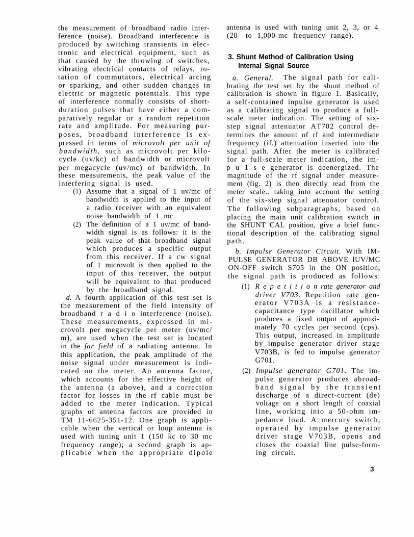
3. Shunt Method of Calibration UsingInternal Signal Source
a. General. The signal path for cal i-brating the test set by the shunt method ofcalibration is shown in figure 1. Basically,a self-contained inpulse generator is usedas a calibrating signal to produce a full-scale meter indication. The setting of six-step signal attenuator AT702 control de-termines the amount of rf and intermediatefrequency (if.) attenuation inserted into thesignal path. After the meter is calibratedfor a full-scale meter indication, the im-p u 1 s e generator is deenergized. Themagnitude of the rf signal under measure-ment (fig. 2) is then directly read from themeter scale.. taking into account the settingof the six-step signal attenuator control.The fol lowing subparagraphs, based onplacing the main unit calibration switch inthe SHUNT CAL position, give a brief func-tional description of the calibrating signalpath.
b. Impulse Generator Circuit. With IM-PULSE GENERATOR DB ABOVE lUV/MCON-OFF switch S705 in the ON position,the signal path is produced as fol lows:
(1)
(2)
R e p e t i t i o n rate generator anddriver V703. Repetition rate gen-e r a t o r V 7 0 3 A i s a r e s i s t a n c e -capacitance type oscillator whichproduces a fixed output of approxi-mately 70 cycles per second (cps).This output, increased in amplitudeby impulse generator driver stageV703B, is fed to impulse generatorG701.
Impulse generator G701. The im-pulse generator produces abroad-b a n d s i g n a l b y t h e t r a n s i e n tdischarge of a direct-current (de)voltage on a short length of coaxiall ine, working into a 50-ohm im-pedance load. A mercury switch,o p e r a t e d b y i m p u l s e g e n e r a t o rd r ive r s t age V703B, opens andcloses the coaxial line pulse-form-ing circuit.
3
F i g u r e 1 . S h u n t m e t h o d o f c a l i b r a t i o n , u s i n g i n t e r n a l s i g n a l s o u r c e .
4
c. Coaxial Relays and Attenuators.(1)
(2)
(3)
(4)
Coaxial relay K702. With this relayin its energized condition, the out-pu t o f the impu l se gene ra to r i scoup led th rough a se t o f r e l aycontacts to 20-db fixed attenuatorAT701.Fixed a t t enua tor AT701 , 20-db .This f ixed at tenuator , coaxial ins t ruc tu re , a t t enua tes the s igna lfrom the impulse generator by 20-db and couples the signal to de-energized coaxial relay K701. Withthis 20-db fixed attenuator in thecalibrating signal path, the outputo f t i e impulse genera to r ag reeswith the engraved numerals on thefront-panel coarse and fine impulsegenerator controls .Coaxial relay K701. With this re-lay in i ts deenergized condit ion,the output of 20-db fixed attenuatorAT701 is coupled through one setof relay contacts to six-step signalattenuator AT702.Six-step signal attenuator AT702.This cartridge-type attenuator hasa flat response to the complete fre-quency range of the test set, from150 kc to 1,000 mc. Six steps ofattenuation are provided by the useof coaxial networks, which resultin a low-vo l t age s t and ing waveratio (swr) at any input frequency.Each at tenuator sect ion is a re-sistive T-pad, in which the serieselements are rod resistors, and theshunt element is a disk-type re-sistor. The geometry of the innterand outer conductors of each atten-uator sect ion produces a 50-ohmline impedance at the input and out-put of each network. Two settingsof the s ix-step s ignal at tenuatorcontrol provide zero attenuation ofthe calibrating signal. The four re-maining settings provide 10-, 20-,40-, or 60-db loss in the rf signalpath; additional attenuation of 10 or20-db is inserted into the if. signalpath (fig. 2). This loss is introducedby operation of relays in the if. stepattenuator, which are controlled by
the setting of six-step signal atten-uator AT702. The division of atten-uation between the rf and the if.signal paths maintains an optimumsignal- to-noise rat io.
d. Typical Tuning Unit. The at tenuateds igna l i s coup led f rom s ix - s t ep s igna lattenuator AT702 to the-input of the tuningunit in use, through mult ipin connectorJ701 (on the main unit) and its mating plug(on the rear of each tuning unit). The tyicaltun ing un i t shown i s r ep resen ta t ive o ftuning units 1 through 4; however, circuitvariat ions exist in each because of thedifferent frequency ranges encountered.
(1)
(2)
(3)
(4)
Rf section. In the tuned rf ampli-f ier , the signal is amplif ied andcoupled to the mixer stage, whicha l so r ece ives a s igna l f rom thelocal oscillator. Sum and differencefrequencies are produced in themixer stage, but only the differencefrequency is accepted by the if .ampl i f i e r .If. step attenuator. The output ofthe mixer s tage is coupled to ath ree - s tep i f . a t t enua to r , whichoperates with rotation of the signalattenuator control (c(4) above).If. amplifier. The difference fre-quency f rom the mixer s t age i samplified by a conventional trans-former-coupled if . amplif ier . Theoutput signal is applied to the sealedde tec to r -e lec t romete r a s sembly .D e t e c t o r and electrometer as-sembly. This assembly is identicaland is interchangeable in all fourtuning units. Two detectors are in-cluded within the assembly. Onede tec to r p rov ides d r ive fo r theaudio amplifier in the main unit e
The other detector provides drive,through high-impedance electro-meter stages, for the vacuum-typevoltmeter indicating circuit in themain unit.
e. Indication Circuits. Two indicat ingcircui ts are provided in the main unit .
(1) Aural. The aural indication is de-rived from electrometer assemblyaudio detector V1. Its output signalis coupled through terminal A1 of
5
(2)
plug (at the rear of the tuning unit)and mating jack J701 (on the in-terior wall of the main unit). Theoutput signal drives audio amplifierV701 in the main unit. The ampli-fied audio voltage produces an auralind ica t ion o f modu la t ed s igna l sw h e n o n e o r t w o h e a d s e t s a r eplugged into PHONES jacks J702and J703, respectively, on the mainunit front panel.Meter. The meter indication is de-rived from meter detector V2 andelectrometers V3-V4. The outputfrom electrometer V3 is coupledthrough terminal 8 of the tuningunit plug and the correspondingterminal of main unit jack J701 tocathode follower V702 .4. The outputfrom electrometer V4 is coupledthrough terminal 11 of the tuningunit plug and the correspondingterminal of main unit jack J701 tocathode follower V702B. These twocathode fol lowers, together withmeter M701, make a bridge-typevacuum-tube voltmeter. The meteremployes a logarithmic 0- to 100-microampere movement, and hastwo scales. One scale is calibratedfrom -6 to +20-db; the second scaleis calibrated from 0 to 10 micro-volt 1
f. Power Supply. The power supply pro-v i d e s s e v e n d i f f e r e n t o u t p u t s f o r t h evarious circuits of the test set (fig. 1). Theinput voltage required at the front-panelPOWER receptacle J721 is 115 volts, 50-to 400-cps. A complete block diagram ofthe power supply is shown in figure 5.
4. Shunt Method of Calibration UsingIncoming Rf Signal
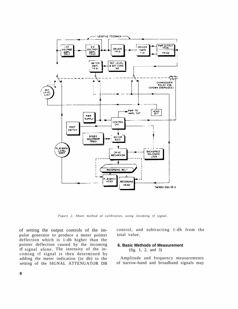
(fig. 2)Figure 2 is a block diagram which shows
detailed operation of the equipment afterthe meter has been calibrated to produce afull-scale deflection by using the output ofthe impul se genera to r a s a ca l ib ra t ingsignal source. Setting the front-panel cali-bration switch to the SERIES CAL& OPER-ATE position changes the circuit connec-tions from those described in paragraph 3.
6
a. Sign a 1 Pickup Device. This b lockdiagram shows one of the three dipoleantennas connected, through the balanced-to-unbalanced transformer (balun) and thered color-coded rf cable, to the SIGNALINPUT jack of the main unit. This color-coded rf cable is part of Electrical CableAssembly Set MX-3410/URM-85. A sepa-rate and distinct dipole antenna is used tocover the full operating frequency rangesof tuning units 2, 3, or 4. When tuning unit1 is in operation, either the loop or verticalantenna must be used, and the test set iscalibrated by the series method (para 5).The other signal pickup devices which re-quire shunt calibration of the meter dependon the method of coupling the signal to theinput of the test set. They are used as de-scribed below:
(1) For conductive measurements, theinput from power or audio-signallines under test is connected to thetest set by special coupling net-works. The following minor com-ponents are used for conductivemeasurements :
Minor componen t( common name)
50-ohm conductive cou-pler for tuning unit 1.
500-ohm conductivecoupler for tuningUnit l.
50-ohm conductive cou-pler for tuning units2, 3, and 4.
500-ohm conductivecoupler for tuningunits 2, 3, and 4.
Nomina l l i ne F r e q u e n c yi m p e d a n c e range
50-150 ohms 150 kc to 30 mc
150-500 ohms 150 kc to 30 mc
50-150 ohms 20 to l,000 mc
150-500 ohms 20 to 1,000 mc
(2) For pinpoint ing the source of rfnoise interference from an instru-ment u h d e r test, the inductivemethod of coupling is used. Thefollowing minor components areused for inductive measurements:
Minor componen t( common name)
Magnetic fieldprobe fortuning unit 1.
C h a r a c t e r i s t i cF r e q u e n c y
r a n g e
Localizes magnetic field 150 kc-30components of rf energy m c .over the frequencyrange of tuning unit l.
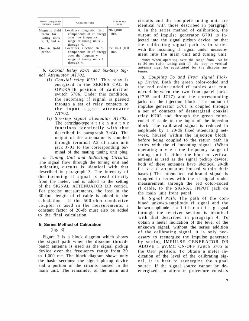
Minor componen t(common name)
Magnetic fieldprobe fortuning units2, 3, and 4.
Electric fieldprobe.
C h a r a c t e r i s t i cF r e q u e n c y
r a n g e
Localizes magnetic field 20-1,000components of rf energy m c .over the frequencyrange of tuning units 2through 4.
Localizes electric field 150 kc-1 ,000components of rf energy m c .over the frequent yrange of tuning units 1through 4.
b. Coaxial Relay K701 and Six-Step Sig-nal Attenuator AT702.
(1)
(2)
Coaxial relay K701. This relay isenergized in the SERIES CAL &OPERATE position of calibrationswitch S706. Under this condition,the incoming rf s ignal is passedthrough a set of relay contacts tot h e i n p u t s i g n a l a t t e n u a t o rAT702.Six-step signal attenuator AT702.The cartridge-type a t t e n u a t o rf u n c t i o n s i d e n t i c a l l y w i t h t h a tdescribed in paragraph 3C (4). Theoutput of the attenuator is coupledthrough terminal A2 of main unitjack J701 to the corresponding ter-minal of the mating tuning unit plug.
c. Tuning Unit and Indicating Circuits.The signal flow through the tuning unit andindicating circuits is identical with thatdescribed in paragraph 3. The intensity ofthe incoming rf s ignal is read direct lyfrom the meter, and is added to the settingof the SIGNAL ATTENUATOR DB control.For precise measurements, the loss in the30-foot length of rf cable is added to thecalculation. If the 500-ohm conductivecoupler is used in the measurements, aconstant factor of 26-db must also be addedto the final calculation.
5. Series Method of Calibration(fig. 3)
Figure 3 is a block diagram which showsthe signal path when the discone (broad-band) antenna is used as the signal pickupdevice over the frequency range from 20to 1,000 mc. The block diagram shows onlythe basic sections: the signal pickup deviceand a portion of the circuits housed in themain unit. The remainder of the main unit
circuits and the complete tuning unit areidentical with those described in paragraph4. In the series method of calibration, theoutput of impulse generator G701 is in-jected into the signal pickup device, so thatthe cal ibrat ing signal path is in serieswith the incoming rf signal under measure-ment into the main unit and tuning unit.
Note: When operating over the range from 150 kcto 30 mc (with tuning unit 1), the loop or verticalantenna must be substituted for the discone an-tenna.
a. Coupling To and From signal Pick-up Device. Both the green color-coded andthe red co lo r -coded r f cab les a re con-nected between the two front-panel jacks(J705 and J717) and the correspondingjacks on the injection block. The output ofimpulse generator G701 is coupled througha set of contacts of deenergized coaxialrelay K702 and through the green color-coded rf cable to the input of the injectionblock. The calibrated signal is reduced inamplitude by a 20-db fixed attenuating net-work, housed within the injection block,before being coupled to the return path inseries with the rf incoming signal. (Whenoperating o v e r the frequency range oftuning unit 1, either the loop or verticalantenna is used as the signal pickup device;both of these antennas have identical 20-dbf i x e d attenuators housed within theirbases.) The attenuated calibrated signal iscoupled in series with the rf signal undermeasurement, through the red color-codedrf cable, to the SIGNAL INPUT jack onthe main unit front panel.
b. Signal Path. The path of the com-bined unkown-amplitude rf signal and theknown-amplitude c a 1 i b r a t i n g signalthrough the receiver section is identicalwith that described in paragraph 4. Toobtain a meter indication of the level of theunknown signal, without the series additionof the calibrating signal, it is only nec-essary to reenergize the impulse generatorby se t t ing IMPULSE GENERATOR DBABOVE 1 µV/MC ON-OFF switch S705 tothe OFF position. To obtain a meter in-dication of the level of the calibrating sig-nal , i t is best to reenergize the signalsource. If the signal source cannot be de-energized, an alternate procedure consists
7
of setting the output controls of the im-
Figure 2. Shunt method of cal ibration, using incoming rf s ignal .
control , and subtract ing 1-db from thepulse generator to produce a meter pointer total value.deflection which is 1-db higher than thepointer deflection caused by the incoming 6. Basic Methods of Measurementrf signal alone. The intensity of the in- (fig. 1, 2, and 3)coming rf s ignal is then determined byadding the meter indication (in db) to the Amplitude and frequency measurementssetting of the SIGNAL ATTENUATOR DB of narrow-band and broadband signals may
8
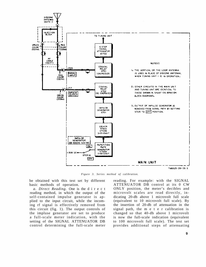
Figure 3. Series method of calibration.
be obtained with this test set by differentbasic methods of operation.
a. Direct Reading. One is the d i r e c treading method, in which the output of theself-contained impulse generator is ap-plied to the input circuit, while the incom-ing rf signal is effectively removed fromthis circuit (fig. 1). The output controls ofthe impluse generator are set to producea fu l l - sca le me te r ind ica t ion , wi th thesetting of the SIGNAL ATTENUATOR DBcontrol determining the ful l-scale meter
reading. For example: with the SIGNALATTENUATOR DB control at i ts 0 CWONLY position, the meter’s decibles andmicrovo l t sca les a re r ead d i rec t ly , in -dicating 20-db above 1 microvolt full scale(equivalent to 10 microvolt full scale). Bythe insertion of 20-db of attenuation in thesignal path, the m e t e r calibration ischanged so that 40-db above 1 microvoltis now the full-scale indication (equivalentto 100 microvolt full scale). The test setprovides addit ional s teps of at tenuat ing
9
networks as shown in the following chart.After the meter has been calibrated by theuse of the self-contained calibrating signal,the impulse generator is disabled and theincoming rf Signal is applied to the re-ce iver . The meter pointer deflection isread d i r e c t 1 y, taking into account thesetting of the SIGNAL ATTENUATOR DBcont ro l . For p rec i se measurements , theloss in the 30-foot length of rf cable isadded to the meter indication. Figures 1and 2 show the signal paths for this methodof measurement, ‘when the shunt method ofcalibration is used.
F u l l - s c a l e m e t e rF u l l - s c a l e m e t e r ind i ca t i on ( i n
SIGNAL ATTENUATOR DB Ind i ca t ion ( i n m i c r o v o l t s u n l e s scon t ro l s e t t i ng db above 1 o the rwise ind i -
mic rovo l t ) cated)
40 60 1,000
60 80 10,000
80 100 100,000
80 (plus the inser- 140 10 voltstion of FixedAttenuator CN-721/URM-45 be-tween the rfcable and theSIGNAL INPUTjack).
b. Substitution Method. A second basicmethod of operating the test set is throughthe subst i tut ion method of measurement.This technique is used when the loop, verti-cal, or discone antenna is the signal pickupdevice for broadband (noise) s ignals . Inthis method of procedure, the known ampli-tude output of the impulse generator issubs t i t u t ed fo r t he p rev ious ly unknownampli tude of the signal under measure-ment. Figure 3 shows the signal path forthis method of measurement, when usingthe series method of calibrating the meter;Essentially, this method reverses the se-quence of operations described in a abovein the following manner:
(1)
(2)(3)
10
The incoming rf signal is appliedto the r ece ive r wi thou t in i t i a l lycalibrat ing the meter. The meterpointer deflect ion and the set t ingof the SIGNAL ATTENUATOR DBcontrol are noted.The incoming rf signal is disabled.The coarse and fine output front-
(4)
panel c o n t r o 1 s of the impulsegenerator are set so that the meterind ica tes the same ampl i tude asthat produced by the incoming rfs ignal .The value of the incoming rf signalis read from the set t ings of theimpulse generator coarse and fineoutput front -panel controls.
7. Introduction to Unit Theory
The signal flow and basic functioning ofthe test set in the shunt and series methodsof calibration have been discussed in thissection. The following sections cover a de-tailed analysis of the test set on a unit-byunit description.
a. Section II analyzes the circuits housedin the main unit, which consists of rf out-put switching and at tenuation, metering,audio amplification, and power supply.
b. S e c t i o n I I I d e s c r i b e s t h e d e t a i l e dfunctioning of tuning unit 1. This unithouses a six-position turret tuner and rfc i r c u i t , i f . input, attenuation, o u t p u tswitching circuits, two separate if. ampli-fier subassemblies (one tuned to 455 kc;the other tuned to 1,600 kc), and the de-t ec to r -e lec t romete r a s sembly .
c. Section IV presents a descript ion ofthe circuits housed in tuning unit 2. Theseare a two-band rf section whose resonanceto incoming rf signals is varied by chang-ing the setting of an i nduc tuner c i r c u i t ,a three-step if . at tenuator, a s ingle if .amplifier subassembly (operating at 10.7-mc cen te r f requency) , and a de tec to r -electrometer assembly which is identicalin all four tuning units.
d. Section V follows the detailed signalpath in tuning unit 3. This unit covers itscomplete frequency spectrum in one band,using an rf tuner whose resonance to in-coming rf signals is varied by gear-drivinga th ree - sec t ion a i r -d ie lec t r i c capac i to r .The if. signal path consists of an if. pre-amplif ier housed in one subassembly, athree-step if. attenuator housed in anothersubassembly , and a ma in i f . ampl i f i e rhoused in a third subassembly. Both the if.preamplif ier and main amplif ier operateat a center frequency of 42 mc. T h e
detector-electrometer a s s e m b 1 y com-pletes the major subassemblies housed inthis tuning unit.
e. Section VI sets forth the distinctivefeatures of tuning unit 4. This unit includestwo separate rf tuners, each of which em-ploys a low-noise rf amplif ier t r iode ofplanar electrode construct ion, operat ing,in a tuned coaxial one-quarter wavelengtht r ansmiss ion l ine . The loca l osc i l l a to r
Section II. THEORY
8. Block Diagram of Main Unit(fig. 1)
Figure 1 shows a block diagram of thefive circuits which are housed in the mainunit. These circuits are the audio ampli-fier, the cathode follower and meter, therf input and impulse generator, the signalattenuator, and the power supply. For acomplete schematic diagram of the mainunit, refer to figure 98. A block diagramdescription of these five major circuits isgiven in paragraphs 9 through 13. Circuitdescription of individual stages of the mainunit is given in paragraphs 14 through 24.
9. Block Diagram of Audio Amplifier(fig. 1)
This circuit receives its driving voltagefrom audio detector V1 in the detector-electrometer assembly through terminalA1 of main unit jack J701 and the corre-sponding terminal on the tuning unit plug.The output of the audio amplifier producesan aural signal which is monitored by con-necting one or two headsets i n t o thePHONES jacks provided on the main unitfront panel.
10. Block Diagram of Cathode Followersand Metering Circuit
(fig. 1)
Cathode followers V702A and V702B re-ceive separate input signals from the de-tector and electrometer assembly withineach tuning unit. Each section of the cathodefollower reproduces its input signal andapplies the difference in amplitude to the
c i rcu i t wi th in each r f tune r i s a con-ventional triode, operating in a tuned one-half wavelength transmission l ine. Theheterodyne output of a silicon diode crystalmixer is coupled to an if. preamplifier, athree-step if . at tenuator, and a main if .amplifier, identical with the signal path oftuning unit 3. The detector electrometera s s e m b 1 y completes the componentshoused in this tuning unit.
OF MAIN UNIT
metering circuit to produce a meter indi-cation. Signal flow in each circuit is asfollows:
a. Cathode Follower V702A. The inputto V702A is coupled from electrometer V3in the tuning unit m through terminal 8 ofmain unit connector J701. The input signalamplitude at V702A is the same as the in-put signal amplitude at electrometer V3,because of the extremely high-impedancecharac te r i s t i c s o f the e lec t romete r c i r -cuit.
b. Cathode Follower V702B. The inputto V702B is coupled from electrometer V4in the tuning unit through terminal 11 ofmain unit connector J701. The input signalamplitude at V702B is approximately one-third of the input signal amplitude to thedetector and electrometer assembly. Thisreduction in signal amplitude is caused bya voltage-divider network at the input tometer detector V2. Therefore, cathode fol-lower V702B produces a smaller amplitudesignal than cathode follower V702A. Thedifference in the outputs of V702B andV702A is applied to the metering circuit.
11. Block Diagram of Rf Input andImpulse Generator Circuits
(fig. 1, 2, and 3)
Since the rf input circuit and the impulsegenerator circuits are closely interrelatedin signal flow, this paragraph describes theeffect of the front-panel calibration switchon their circuit operation. The positioningof the calibration switch depends on theantenna or coupler which is used at theinput to the test set. Shunt calibration (a
11
below) is required when the dipole antennaor coupler devices are used. Series cali-bration (b below) is required when the dis-cone, loop, or vertical antenna is used. Ine i the r se r i e s o r shun t ca l ib ra t ion , theset t ing of the s ix-step s ignal at tenuator(c below) affects the signal path.
a. Shunt Calibration Condition (fig. 1 and2). The following two circuit conditionsexist with the calibration switch set at theSHUNT CAL position.
(1)
(2)
The calibrating signal voltage fromimpulse generator G701 has a pathof continuity through coaxial relayK702 to the input of 20-db fixedattenuator AT701. The calibratingsignal is decreased in amplitude bya ratio of 10 to 1 (20-db), and isapplied through coaxial relay K701to the input of six-step signal at-tenuator AT702.The incoming rf signal applied toSIGNAL INPUT jack J705 (fig. 2)i s e f fec t ive ly removed f rom theinput to the test set. Therefore, noincoming signal from the antennaor coupler can affect the meter in-dication when the test set is beingca l ib ra t ed by the shun t me thod .
b. Series Calibration and Operate Con-di t ion (fig. 2 and 3). The following twocircuit conditions exist with the calibrationswitch set at the SERIES CAL& OPERATEposition.
(1)
(2)
An incoming signal, applied fromthe an tenna o r coup le r th roughSIGNAL INPUT jack J705, has apath of continuity through coaxialrelay K701 to six-step signal atten-uator AT702.The calibrating signal voltage fromimpulse generator G701 is inter-rupted from the input to 20-db fixedattenuator AT701 (f ig. 1) by de-energizing c o a x i a 1 relay K702Therefore, 20-db f ixed at tenuatorAT701 is effectively removed fromthe calibrating signal path and thefull cal ibrat ing signal voltage isavailable at front-panel IMPULSEOUTPUT jack J717 (fig. 3).
c. Signal Attenuating Circuit. Figure 3shows that the incoming rf signal passes
12
through six-step signal attenuator AT702before application to the input of the tuningunit. The purpose of the signal attenuatoris to insert either zero or a fixed amountof resistive attenuation in the rf and if.s ignal path. This circuit arrangement isdescribed in paragraph 12.
12. Block Diagram of Signal AttenuatorAT702 Circuitry
(fig. 4)
Figure 4 shows the threefold functioningof the six-step SIGNAL ATTENUATOR DBcontrol . This block diagram is based onplacing the front-panel calibration switchin the SERIES CAL & OPERATE position(fig. 2). The s h a f t of the front-panelSIGNAL ATTENUATOR DB control drivesth ree separa te swi tches , which opera tecircuits as described below:
a. Rf Attenuating Circuit. The incomingrf signal is coupled through front-panelSIGNAL INPUT jack J705 and coaxial relayK 7 0 1 . T h i s r e l a y i s e n e r g i z e d i n t h eSERIES CAL & OPERATE position of thecalibration switch, and a path of continuityis created to the input of rf six-step signalattenuator AT702. The six positions of theSIGNAL ATTENUATOR DB control havethe fol lowing effect on the incoming rfsignal:
(1)
(2)
In the 0 SUBST. ONLY position,zero attenuation is inserted in the.rf signal path. Since the test setinput circuit is not terminated witha 50-ohm impedance in this positiono f t h e a t t e n u a t o r , q u a n t a t i v emeasurements are meaningful onlyif the substitution method of opera-tion (para 6b) is used. The 0 SUBST.ONLY position of the attenuator isusua l ly used fo r t ak ing r e l a t ivem e a s u r e m e n t s o f b r o a d b a n d(noise) signal amplitude with themagnetic field probe, the electricfield probe, or the conductive cou-p l e r s .In the 0 CW ONLY position, 10-dbof attenuation is inserted in the rfs ignal path. This posi t ion of thecontrol provides a 50-ohm termi-nation to match the characteristic
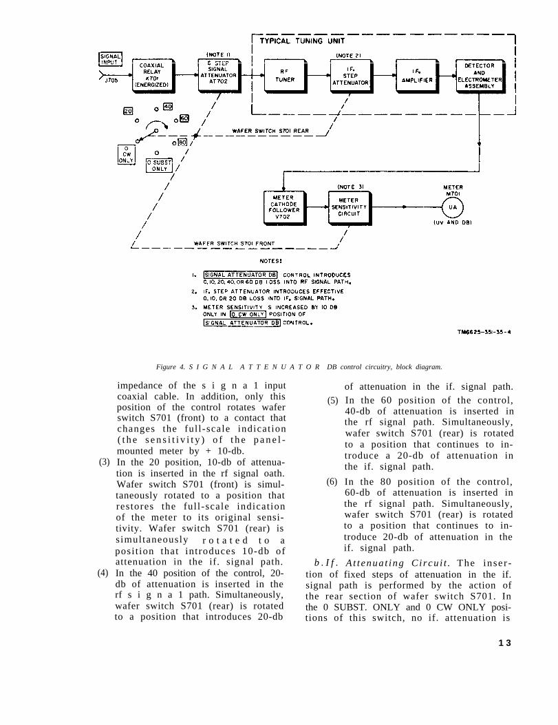
(3)
(4)
Figure 4. S I G N A L A T T E N U A T O R DB control circuitry, block diagram.
impedance of the s i g n a 1 inputcoaxial cable. In addition, only thisposition of the control rotates waferswitch S701 (front) to a contact thatchanges the ful l-scale indicat ion( t h e s e n s i t i v i t y ) o f t h e p a n e l -mounted meter by + 10-db.In the 20 position, 10-db of attenua-tion is inserted in the rf signal oath.Wafer switch S701 (front) is simul-taneously rotated to a position thatrestores the ful l-scale indicat ionof the meter to its original sensi-tivity. Wafer switch S701 (rear) iss imultaneously r o t a t e d t o aposi t ion that introduces 10-db ofattenuation in the if. signal path.In the 40 position of the control, 20-db of attenuation is inserted in therf s i g n a 1 path. Simultaneously,wafer switch S701 (rear) is rotatedto a position that introduces 20-db
(5)
(6)
b . I f .tion of
of attenuation in the if. signal path.In the 60 position of the control,40-db of attenuation is inserted inthe rf signal path. Simultaneously,wafer switch S701 (rear) is rotatedto a position that continues to in-troduce a 20-db of attenuation inthe if. signal path.
In the 80 position of the control,60-db of attenuation is inserted inthe rf signal path. Simultaneously,wafer switch S701 (rear) is rotatedto a position that continues to in-troduce 20-db of attenuation in theif. signal path.
At tenua t ing C i rcu i t . The inse r -fixed steps of attenuation in the if.
signal path is performed by the action ofthe rear section of wafer switch S701. Inthe 0 SUBST. ONLY and 0 CW ONLY posi-tions of this switch, no if. attenuation is
1 3
inserted in the signal path. In the 20 posi-t ion, the -150-volt output of the powersupply has a path of continuity to one ofthe two relays in the if. step attenuator.When energized, this relay inserts a 10-db resis t ive pad in the i f . s ignal path.However, in the 40, 60, and 80 positionsof S701, the -150-volt output of the powersupply also has a path of continuity to thesecond relay in the if . s tep at tenuator .When bo th r e l ays in the i f . a t t enua to rassembly are energized, a total networkresul t ing in 20-db of at tenuat ion is in-serted in the if. signal path.
c. Meter Sensitivity Circuit. The 0 CWONLY position of the SIGNAL ATTENU-ATOR DB control inserts a 50-ohm re-sistive termination in the rf signal pathfo r p roper impedance match ing . Whi lethis termination produces a 10-db loss inrf s ignal ampli tude, wafer switch S701(front) removes a multiplier resistor fromthe dc metering signal path. The value ofthis multiplier resistor is equivalent to a10-db gain in meter sensitivity; the meterfull-scale indication is effectively changedfrom 10 microvolt to 1 microvolt. There-fore, with 10-db of at tenuation insertedin the rf signal path, the overall result iszero attenuation in the combined rf and dcmeter signal path.
13, Block Diagram of Power Supply(fig. 5)
The power supply provides al l of thepower requ i rements fo r the c i r cu i t s inthe main unit and in the tuning unit. As impl i f i ed r ep resen ta t ion o f the powersupply is shown in the shunt calibrationblock diagram (fig. 1 and 2). The flow ofpower and the development of low-voltagealternating current (ac) and rect if ied dcvoltages is shown in the detai led blockdiagram (fig. 5).
a. Ac Input and Output Power. Ac inputis connected to the main unit at POWERreceptacle J721. The voltage is fed throughPOWER switch S710 to interlock switchS711 and protective fuse F701. The inter-lock switch is closed when a tuning unit isplugged into the opening provided at theleft side of the main unit. When a tuning
unit is removed from the main unit, inter-lock switch S711 opens and the ac inputpower path is interrupted from the re-mainder of the circuitry. The closed con-dition of interlock switch S711, or the useo f t h e a l i g n m e n t h a r n e s s , p e r m i t s a cpower to flow through vibrating-type reg-ulator K703 into the primary windings,terminals 1 and 2, of power transformerT702. One secondary winding, terminals17 and 18, s teps down the 115-volt acinput to 6.3-volts ac output, which is usedas hea te r power by a l l e l ec t ron tubesexcept audio amplifier V701 and the stageshoused in the detector and electrometerassembly . Another secondary winding,terminals 14 and 16, steps down the 115-volt ac input to 5.8-volts ac. This poweri s used in the hea te r c i r cu i t o f aud ioamplifier V701 and detectors V1 and V2in the electrometer assembly.
b. +150 Volt Unregulated Power Circuit.The 115-volt ac power at the primary ofpower t r ans fo rmer T702 i s s t epped upin voltage through a center- tapped sec-ondary winding, terminals 3, 4, and 5.Para l l e l - connec ted rec t i f i e r s V704 andV705 produce a dc output of approximately+175-volts with respect to chassis ground.This output is filtered and dropped in valueby the double L-type filter, which consistsof reactor L722 and capacitor C734, andis used as 150-volt B+ power for all stagesexcept the local oscillators in the tuningunits and al l tubes in the detector ande lec t romete r c i r cu i t . The dc ou tpu t o fV704-V705 is also used as a referencevoltage for vibrating-type regulator K703.This reference voltage is applied to thecoil of the vibrating-type regulator, whichapplies varying amounts of resistance inseries with the ac input power, dependingon input line fluctuations and output loadvariat ions.
c. +105-Volt Regulated Power Circuit.The 105-volt regulated output is derivedfrom the 150-volt power supply. This 105-volt output is regulated by voltage reg-ulator tube V708, and is used as B+ volt-age by the local oscillators in each tuningunit .
d. -150- Volt Regulated Power Circuit.Metallic rectifier CR706 is connected to
14
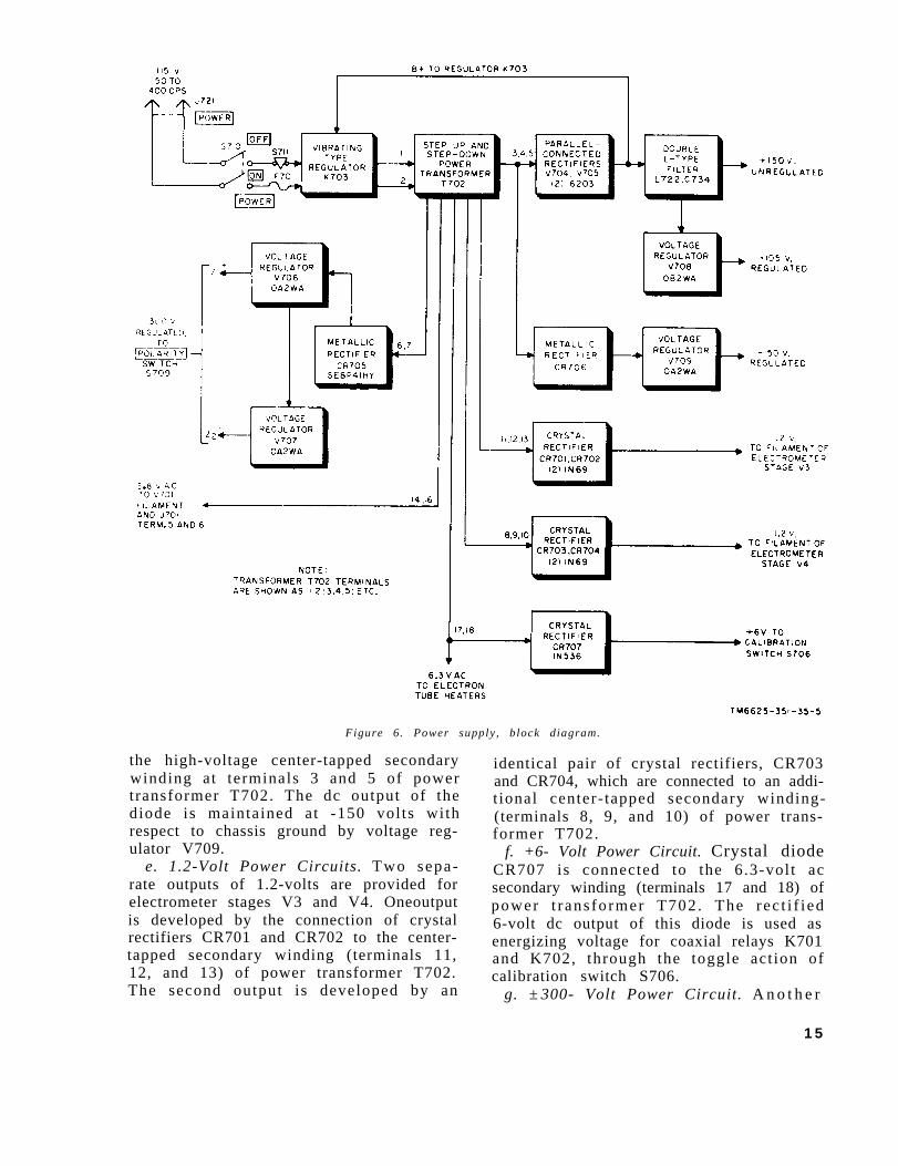
Figure 6. Power supply, block diagram.
the high-voltage center-tapped secondarywinding at terminals 3 and 5 of powertransformer T702. The dc output of thediode is maintained at -150 volts withrespect to chassis ground by voltage reg-ulator V709.
e. 1.2-Volt Power Circuits. Two sepa-rate outputs of 1.2-volts are provided forelectrometer stages V3 and V4. Oneoutputis developed by the connection of crystalrectifiers CR701 and CR702 to the center-tapped secondary winding (terminals 11,12, and 13) of power transformer T702.The second output is developed by an
identical pair of crystal rectifiers, CR703and CR704, which are connected to an addi-t ional center- tapped secondary winding-(terminals 8, 9, and 10) of power trans-former T702.
f. +6- Volt Power Circuit. Crystal diodeCR707 is connected to the 6.3-volt acsecondary winding (terminals 17 and 18) ofpower t rans former T702 . The rec t i f i ed6-volt dc output of this diode is used asenergizing voltage for coaxial relays K701and K702, through the toggle act ion ofcalibration switch S706.
g. ±300- Volt Power Circuit. A n o t h e r
1 5
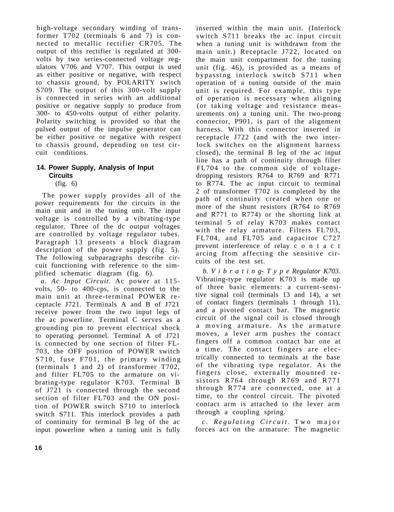
high-voltage secondary winding of trans-former T702 (terminals 6 and 7) is con-nected to metal l ic rect if ier CR705. Theoutput of this rectifier is regulated at 300-volts by two series-connected voltage reg-ulators V706 and V707. This output is usedas either positive or negative, with respectto chassis ground, by POLARITY switchS709. The output of this 300-volt supplyis connected in series with an additionalpositive or negative supply to produce from300- to 450-volts output of either polarity.Polarity switching is provided so that thepulsed output of the impulse generator canbe either positive or negative with respectto chassis ground, depending on test cir-cuit conditions.
14. Power Supply, Analysis of InputCircuits
(fig. 6)
The power supply provides al l of thepower requirements for the circuits in themain unit and in the tuning unit. The inputvoltage is controlled by a vibrating-typeregulator. Three of the dc output voltagesare controlled by voltage regulator tubes.Paragraph 13 presents a block diagramdescription of the power supply (fig. 5).The following subparagraphs describe cir-cuit functioning with reference to the sim-plified schematic diagram (fig. 6).
a. Ac Input Circuit. Ac power at 115-volts, 50- to 400-cps, is connected to themain unit at three-terminal POWER re-ceptacle J721. Terminals A and B of J721receive power from the two input legs ofthe ac powerline. Terminal C serves as agrounding pin to prevent electrical shockto operating personnel. Terminal A of J721is connected by one section of filter FL-703, the OFF position of POWER switchS710 , fuse F701 , the p r imary wind ing(terminals 1 and 2) of transformer T702,and filter FL705 to the armature on vi-brating-type regulator K703. Terminal Bof J721 is connected through the secondsection of filter FL703 and the ON posi-tion of POWER switch S710 to interlockswitch S711. This interlock provides a pathof continuity for terminal B leg of the acinput powerline when a tuning unit is fully
inserted within the main unit. (Interlockswitch S711 breaks the ac input circuitwhen a tuning unit is withdrawn from themain unit . ) Receptacle J722, located onthe main unit compartment for the tuningunit (fig. 46), is provided as a means ofbypass ing in t e r lock swi tch S711 whenoperation of a tuning outside of the mainunit is required. For example, this typeof operat ion is necessary when al igning(or taking voltage and resistance meas-urements on) a tuning unit. The two-prongconnector, P901, is part of the alignmentharness. With this connector inserted inreceptacle J722 (and with the two inter-lock switches on the al ignment harnessclosed), the terminal B leg of the ac inputline has a path of continuity through filterFL704 to the common side of voltage-dropping resistors R764 to R769 and R771to R774. The ac input circuit to terminal2 of transformer T702 is completed by thepath of continuity created when one ormore of the shunt resistors (R764 to R769and R771 to R774) or the shorting link atterminal 5 of relay K703 makes contactwith the relay armature. Fil ters FL703,FL704, and FL705 and capacitor C727prevent interference of relay c o n t a c tarcing from affect ing the sensi t ive cir-cuits of the test set.
b. V i b r a t i n g- T y p e Regulator K703.Vibrating-type regulator K703 is made upof three basic elements: a current-sensi-tive signal coil (terminals 13 and 14), a setof contact fingers (terminals 1 through 11),and a pivoted contact bar. The magneticcircuit of the signal coil is closed througha m o v i n g a r m a t u r e . A s t h e a r m a t u r emoves, a lever arm pushes the contactfingers off a common contact bar one ata t ime . The con tac t f ingers a re e lec -trically connected to terminals at the baseof the vibrat ing type regulator . As thef inge r s c lose , ex te rna l ly moun ted re -s i s to r s R764 th rough R769 and R771th rough R774 a re connec ted , one a t atime, to the control circuit. The pivotedcontact arm is attached to the lever armthrough a coupling spring.
c . R e g u l a t i n g C i r c u i t . T w o m a j o rforces act on the armature: The magnetic
16
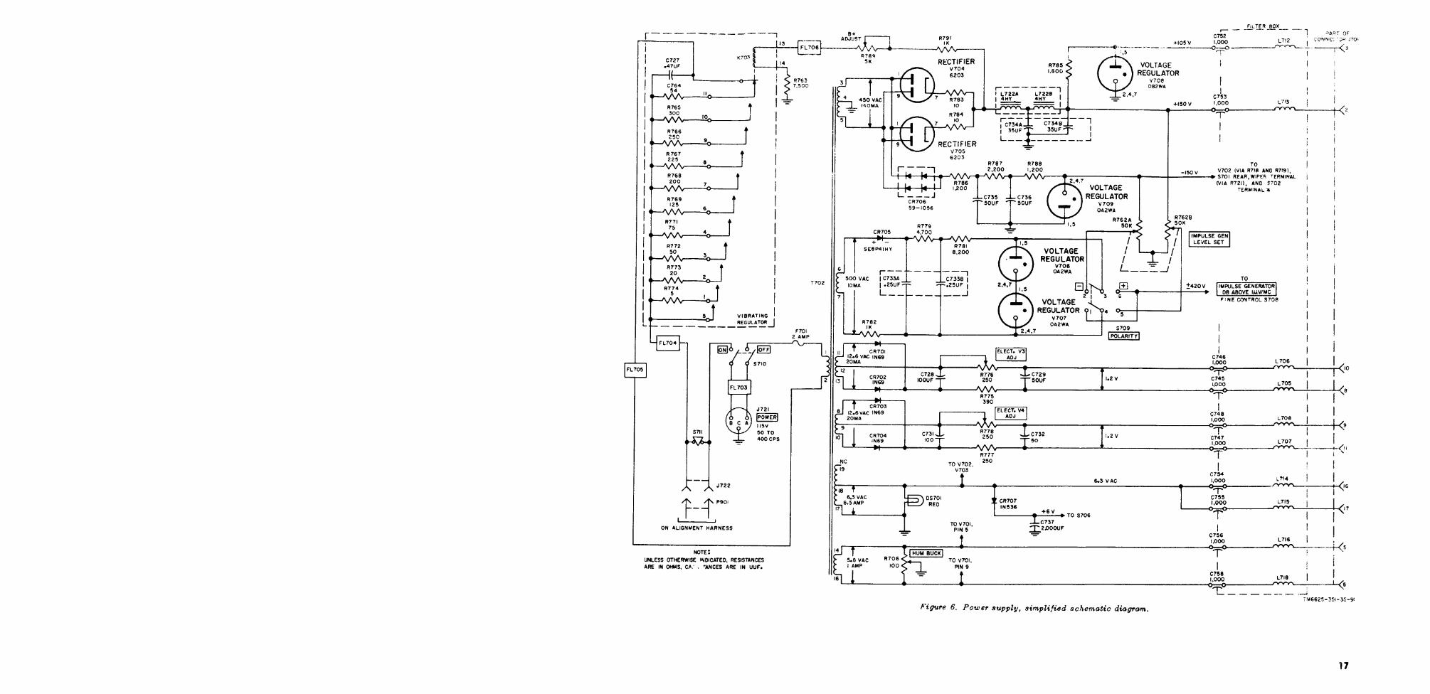
pull through K703 signal coil, which re-ceives energizing power from rectif iersV704 and V705, and the pull of the springs.If the current through the signal coil iskept constant at a nominal value, the mag-netic pull will increase in a linear man-ner as the armature moves to close moreand more f ingers . The a rmature i s inmechan ica l equ i l ib r ium on ly when thecurrent flowing through signal coil K703is at its nominal B+ value. For all othervalues of signal coil current, equilibriumis upset and the armature moves to openor c lose the con tac t f inge r s . Res i s to r sR764 through R769 and R771 through R774are connected into the control circuit pathfrom one side of interlock switch S711 tot e r m i n a l 1 of T702 primary winding.Therefore, the function of the vibrating-type regulator is to control the amount ofresistance in the ac input power line cir-cuit. The B+ adjust control (R789) is usedto se t t he nomina l amoun t o f cu r ren tthrough K703 signal coil. Resistor R791functions as a current-limiting device andis connected between the output of recti-fiers V704-V705 and the B+ adjust control.Filter FL706 filters the current in the B+line; resistor R763 functions as a furthercurrent-l imit ing device for K703 signalcoi l .
15. Power Supply, Analysis ofOutput Circuits
(fig. 6)
The power supply develops outputs of+ 1 5 0 - v o l t s , + 1 0 5 - v o l t s , + 6 - v o l t s , a n d-150-volts with respect to chassis ground.Two additional outputs, each of 1.2-voltsdc, are produced. A 5.8-volt ac and a 6.3-volt ac output is developed for electrontube heater power. A final circuit develops±300-volts dc for use by the coaxial delayline charging circuit of impulse generatorG701.
a. +150- Volt and +105 Volt Dc PowerCircuit . One secondary winding ( termi-nals 3, 4, and 5) of T702 steps up the in-put voltage to 450-volts. Rectifier tubesV704 and V705, connected in a full-wavecircuit , rect ify the stepped up voltage.Res i s to r s R783 and R784 a re vo l t age -
d ropp ing re s i s to r s . The f luc tua t ing dcvoltage is smoothed by a choke-input filterne twork cons i s t ing o f L722A, C734A,L722B, and C73413. The +150-volt filteredoutput is connected to terminal 2 of mainunit receptacle J701 as plate and screenvoltage for al l tubes in the tuning unitexcept the oscillator stage in the rf tuner.Res i s to r R785 se rves a s an add i t iona lvo l t age -d ropp ing r e s i s to r t o deve lop a+105-volt output, which is controlled byvoltage regulator V708. This output isconnected to terminal 3 of J701 as platevo l t age fo r the osc i l l a to r t ubes in thetuning unit.
b. - 150- Volt DC Power Circuit . T h efull output (terminals 3 and 5) of T702 sec-ondary winding (a above) is also connectedto the cathodes of the dual full-wave recti-fier CR706. The negative output is filteredby resistors R786 and R787 and capacitorsC735 and C746 . Res i s to r R788 i s t hevoltage-dropping resis tor in series withregulator V709, which holds the output at-150-volts with respect to chassis ground.This potential is used as grid and cathodevoltage by cathode follower stage V702,as energizing voltage for the two relays inthe if. step attenuator of the tuning unit,and as the source of bias voltage for theif. amplifiers in the tuning unit..
c. +6- Volt DC Power Circuit . C r y s t a lrectifier CR707, connected in a half-wavecircuit , rect if ies the 6.3-volt ac powerdeveloped across terminals 17 and 18 ofT702. The dc output, filtered by capacitorC737, is connected to calibration switchS 7 0 6 , a n d i s u s e d t o e n e r g i z e e i t h e rcoaxial relay K701 or K702, depending onthe switch position.
d. 1.2- Volt DC Power Circuit for Elec-trometer V3. One secondary winding (ter-minals 11, 12, and 13) steps down the acinput voltage to 12.6-volts. Crystal recti-f i e r s CR701 and CR702 , connec ted infull-wave circuit , rect ify the secondaryvoltage. The output is f i l tered by a pi-sect ion f i l ter , consist ing of variable re-s i s t o r R 7 7 6 a n d c a p a c i t o r s C 7 2 8 a n dC729. Resistor R776 is used to adjust thedc output of the rect if iers to 1.2-volts ,which is connected to terminals 8 and 10
19
of main unit receptacle J701. These ter-minals supply heater power for electrom-eter V3, in the detector and electrometerassembly of the tuning unit. Resistor R775is a voltage-dropping resistor.
e. 1.2- Volt Dc Power Circuit for Elec-trometer V4. One secondary winding (ter-minals 8, 9, and 10) of T702 performs thesame function as that described in d above.Crystal rectifiers CR703 and CR704, con-nected in a full-wave circuit, rectify thesecondary voltage. The output is filteredby a p i - sec t ion f i l t e r t ha t cons i s t s o fva r i ab le r e s i s to r R778 and capac i to r sC731 and C732. Resistor R778 is used toadjust the dc output to 1.2 -volts, which isconnected to contacts 9 and 11 of mainun i t r ecep tac le J701 . These t e rmina l ssupply heater power for electrometer V4,in the detector and electrometer assemblyof the tuning unit . Resis tor R777 is avoltage-dropping resis tor .
f. 5.8- Volt Ac Power Circuit. One sec-ondary winding (terminals 14 and 16) ofT702 provides heater current for audioamplifier V701 and for the two detectorstages housed ‘in the tuning unit. Potenti-ometer R706 is connected across the 5.8-volt ac input to the heater terminals ofV701, pins 5 and 9. The arm of R706 oper-ates at chassis ground potential. The 5.8-volt ac input voltage across V701 heateris divided in half by setting the arm ofpotentiometer R706 at the midpoint of itsrange. This setting of R706 tends to cancelout any hum that may be picked up andamplified by audio amplifier V701. Thefull 5.8-volts ac is available at terminals5 and 6 of main unit receptacle J701. Themating plug at the rear of a tuning unitapplies this 5.8-volt ac heater power tothe two detector stages within the detectorand electrometer assembly.
g . 6 . 3 - V o l t A c P o w e r C i r c u i t . O n ecenter-tapped secondary winding of trans-former T702 (terminals 17 and 18) pro-vides heater current for all tubes and pilotlamps in the equipment, except for thosetubes housed within the detector and elec-t romete r assembly . Hea t e r power i scoupled through termimls 16 and 17 of
main unit receptacle J701 to the matingplug on the tuning unit.
h. +300- Volt Dc Power Circuit. O n esecondary winding ( terminals 6 and 7)steps up the input voltage to 500-volts. Thevoltage is r e c t i f i e d by a half-wavemetallic-type rectifier CR705. The recti-f ier output is f i l tered by a pi- type net-work which consists of resistor R779 andthe two sections of a dual capacitor C733.Resistor R781 is the voltage-dropping re-sistor for the series -connected regulatorsV706 and V707, which holds the output at300-volts . Resistor R782 is a vol tage-dropping resis tor . The output can be re-versed in polarity by setting POLARITYswitch S709 to either its plus or minusposition. The terminals of this double-pole double-throw (dpdt) switch are tiedto both the negative 150-volt output (fromV709) and the posi t ive 150-volt output(from V704-V705) for reference. Circuitoperation is as follows:
(1) The high side of variable resistorR762B is connected to the +150-volt output of rectifiers V704 andV705. The low side of R762B isconnected to chassis ground. WhenPOLARITY switch S709 is set to its+ pos i t ion , the va r i ab le a rm ofR762B has a path of continuity tothe negative 300-volt output fromthe cathode of regulator V707. Thiscircuit arrangement can produce atotal usable output which is the sumof +150-volts to chassis ground,and the potential difference fromchassis ground to -300-volts. Thetotal potential which can be ob-tained across this network is 450-volts. A variation of 150-volts isobtained by rotat ing the arm ofIMPULSE GEN LEVEL SET con-trol R762. The setting of the poten-t iometer determines the chargingvoltage, applied through the 10-dbstep coarse attenuator control S708to impulse generator G701. Duringcalibration of the equipment, thevariable arm of R762 is set so thatthe output amplitude from impulsegenerator G701 is equivalent to theoutput from an external impulse
2 0
(2)
(3)
genera to r which func t ions a s astandard for calibrating purposes.The high side of variable resistorR762A is connected to the -150-volt output of regulator V709. Thelow side of R762A is connected tochassis ground. When POLARITYswitch S709 is set to its minus (-)position, the variable arm of R762Awill be connected to the positive300-volt output at the plate of volt-age regu la to r V706 . The c i rcu i tarrangement is similar to that de-sc r ibed in (1 ) above , bu t i s o fopposi te polari ty. A total usableoutput of 450-volts can be obtainedby adding the -150-volts (from theh igh s ide o f R762A to chass i sground) to the +300-volts (fromchassis ground to the positive out-put of V706 and V707). A variationof 150-volts is obtained by rotatingthe arm of IMPULSE GEN LEVELSET control R762. The setting ofthe potentiometer determines thecharging voltage, applied through10-db step coarse attenuator con-t ro l S708 to impu l se gene ra to rG701 (1) above).The positive and negative positionsof POLARITY switch S709 are pro-vided so that the effects of either
positive or negative output pulsesfrom impulse generator G701 canbe observed when performing noisemeasurements .
16. Audio Amplifier, Stage Analysis(fig. 7)
Audio amplifier V701 is a dual triode,which receives its input signal from audiodetector V1 in the electrometer assembly(fig. 1) and delivers its output signal toone or two headsets. The two sections ofV701 function as two separate amplifiers,as described below.
a. First Audio Amplif ier V701A. T h eaudio voltage at terminal Al of connectorJ701 is applied to the grid resistor, whichconsists of VOLUME control R701, througha shielded cable. When the meter is usedas the indicating device for the signal undermeasurement, the full output of the audiodetector in the electrometer assembly isapplied to the first audio amplifier. Whenthe sl ideback technique of operat ion isused (para 22), the setting of the SLIDE-BACK control applies a negative bias tothe plate of the audio detector stage. Underthis condition, only the peaks of the signalunder measurement , wi th an ampl i tudehigher than the detection level set by theSLIDE BACK control, will be heard in the
F i g u r e 7 . A u d i o a m p l i f i e r s V 7 0 1 A a n d V 7 0 1 B , s i m p l i f i e d s c h e m a t i c d i a g r a m .
21
headset. Depending on the position of thearm of the VOLUME control, all or partof the audio voltage is applied to the con-trol grid, pin 2, of V701A. Cathode bias isdeveloped across resistor R702, which isbypassed by capacitor C702. The signalvo l t age i s deve loped ac ross p l a t e loadresistor R703, which is connected to the+150-volt output of the power supply. Ca-pac i to r C701 se rves to bypass any i f .component which may still be present inthe input signal. Capacitor C703 couplesthe amplified output from the plate, pin 1,of V701A to the input of the second audioamplif ier .
b. Second Audio Amplifier V701B. T h eamplified audio voltage coupled throughcapacitor C703 and parasi t ic suppressorR705 is developed across grid resis torR704. Cathode bias is provided by thevoltage drop across unbypassed cathoderesistor R707. Plate voltage for V701B issupplied from the +150-volt supply throughthe primary winding, terminals 1 and 2, ofoutput t ransformer T701, The amplif iedaudio voltage from the plate, pin 6, ofV701B is coupled to transformer T701.Audiofrequencies within the range from150- to 5,000-cps, flat within 8-db of the1 ,000-cps ampl i tude , a re t r ans fo rmer -coupled by the secondary winding, ter-minals 3 and 4, to the input of rf filterFL701. The filter circuit, which consistsof feedthrough capacitor C705 and rf coilL719, prevents rf signals which may bepicked up by the headsets or the headsetcords f rom en te r ing the t e s t se t . TwoPHONE jacks, which are integral parts off i l ter FL701, permit connecting one ortwo headsets to the final output signal fromaudio amplifier V701B.
17. Meter Cathode Follower V702 andMetering Circuit, Stage Analysis
(fig. 8)
a. General. Cathode follower V702 is adual triode which is connected as a bridge-type amplifier (B, fig. 8) to provide drivefor the panel-mounted meter and for eithera recorder or the remote meter, when con-nected to RECORDER EXT METER jackJ704. The dc input voltages to sections A
and B of the bridge-type amplif ier arederived from meter detector V2 and high-impedance electrometer stages V3 and V4(para 32) which are housed within thesealed assembly of each tuning unit (fig. 1).In the static condition of the bridge ampli-fier, R715 is adjusted SO that the potentialat C and D are equal, and no current flowsthrough the metering circuit (0 MICRO-VOLTS). When signals (negative voltages)are applied to the grids of electrometertubes V3 and V4 (fig. 19), the negativegoing outputs taken from the cathodes areapplied to the grids of V702A and V702Brespectively. Negative going voltages onthe grids of V702A and V702B cause thedc plate resistance of each triode to in-crease. Meter detector tube V2 and elec-trometer tubes V3 and V4 are arrangedin a signal voltage-divider circuit so thatV702A rece ives one- th i rd more s igna lvoltage than V702B. Therefore, the dcplate resistance of V702A increases morethan that of V702B. This will cause pointC to become negative with respect to pointD and current will flow through the meter-ing circuit.
b. Cathode Follower V702 (A, fig. 8).The two sections of cathode follower V702are connec ted in a nea r ly symmet r i ca lcircuit . In the cathode circuit , one re-sistor (R712) for V702A is fixed; the cor-responding resistor (R715) for V702 B isva r i ab le . In th i s manner , the vo l t agesacross the bridge circuit can be equalizedby adjusting ZERO ADJ control R715 inthe absence of an incoming signal. Fixedres i s to r s R712 and R713 se rve a s thecathode load resistor , connected to the-150-volt output of the power supply, forV702A. Resistors R714 and R715 functionidentically in the corresponding circuit forV702B.
(1) Grid circuits. Resistor R719 is thegrid return for V702A; an identicalvalue resistor , R718, is the gridreturn for V702B. Since both theg r i d r e t u r n r e s i s t o r s a n d t h ecathode resistors are connected tothe -150-volt output of the powersupply, the bias voltage for eachsection of V702 is determined bythe current flowing through their
22
(2)
(3)
18. CW
r e spec t ive load re s i s to r s , R712 ,R713, R714 and R715.Plate circuits. The plates of eachsection of cathode follower V702are directly connected to the +150-volt output of the power supply.Detailed circuit description. Sincea detailed circuit description of thecathode fol lower depends on theposition of function switch S702,the description of current flow inthe metering circuit is covered inthe following paragraphs of func-tion switch operation.
AVERAGE Position ofFunction Switch
(fig. 8)
The fol lowing subparagraphs describethe circuit conditions for the C W AVER-AGE position of function switch S702. Fig-ure 8 shows that the output of cathodefollower V702A is developed across loadresistor R712 and cathode-bias resis torR713. With SIGNAL ATTENUATOR DBwafer switch S701 in any position except0 CW ONLY, the signal is coupled throughmete r mul t ip l i e r r e s i s to r R722 to t e r -minal 2 of function switch S702 (rear). Inthe 0 CW ONLY position of S701, resistorR722 is bypassed by the wiper and ter-minal 2 of the switch; the meter is then10-db more sensi t ive than in any otherposition of S701 (para 12c). The varioussect ions of f ict ion switch S702 providea path of continuity for the metering signalas follows:
a . S702 Rear , Sec t ion X . C o n t a c t i smade between terminals 2 and 3 so thatthe metering signal has a path of continuitythrough rf filter FL702. This filter housesfeedthrough capacitors C706 and C707, rfcoils L720 and L721, and fixed resistorR725. Resistor R725 functions as a metermultiplier with no phone plug inserted intoRECORDER EXT METER jack J704. Theinsertion of a phone plug into jack J704removes R725 from the metering signalpath and substitutes the internal resistanceof ei ther the remote meter or a record-ing meter (depending on the device usedat the remote site) into the meter multi-
p l i e r c i r c u i t . T h e m e t e r i n g s i g n a l i scoupled to the negative terminal of M701and continues through the meter move-ment to the positive terminal of M701.
b. S702 Front , Sect ion Y. C o n t a c t i smade between terminals 1 and 2 so thatthe metering signal has a path of continuitythrough IF. CATHODE FOLLOWER ADJswitch S704, which normally is closed.Switch S704 is provided as a chassis ad-justment control for peaking the if. cathodefollower stages in the if . amplif iers ofturning units 2, 3, and 4. (There is no if.cathode follower in tuning unit 1.) Findres i s to r R717 i s in se r t ed in the me te rpa th a s an add i t iona l me te r mul t ip l i e rwith the switch in its open position. Anaddit ional meter mult ipl ier is necessarybecause adjustment of the peaking coils inthe if. cathode followers of tuning units 2,3, and 4 requires overdriving the meterbeyond its full-scale indication. CapacitorC708 damps the meter movement whenMETER DAMP switch S703 is thrown toits ON position or held in its MOM posi-t ion. This switch, which provides an acpath through capacitor C708 and resistorR723 across the meter terminals, is usedwhen low-signal levels cause erratic meterpointer fluctuations. The metering signalhas a return path fo the +150-volt powersupply through the normally closed con-tacts of switch S704, fixed resistor R716,ZERO ADJ control R715, and V702B.
c. S702 Front Section Z. C o n t a c t i smade between terminals 2 and 3 only in theC W AVERAGE position of the functionswitch. Under this condition, the 6.3-voltac output from the power supply passesthrough feedthrough capacitor C751 and rfcoil L711 in the filter box, to terminal 18of main unit receptacle J701. The matingplug at the rear of the tuning unit appliesthis 6.3-volt ac potential to the heaters oftwo thermal relays in the detector andelectrometer assembly. The load imped-ance of the two detectors in the electro-meter assembly is reduced with the heatersof the relays energized. This action isequivalent to lowering the t ime-constantin the detector charging circuit. The pur-pose of this circuit is to enable the elec-trometers to measure the average envelope
2 3
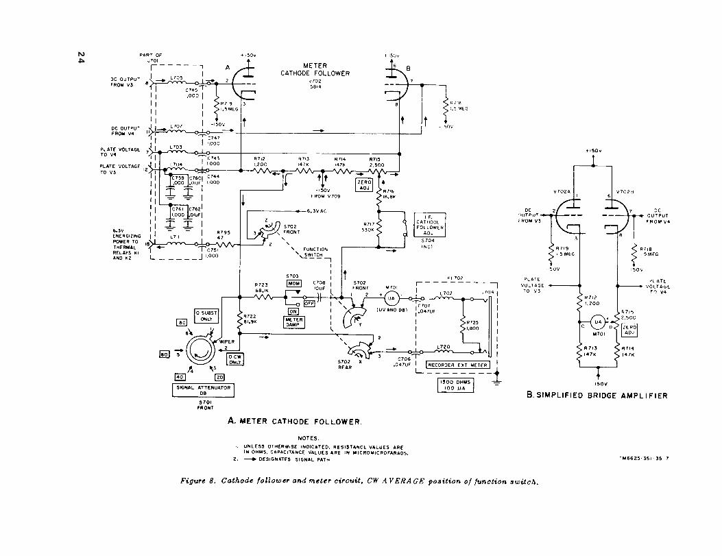
Figure 8.
24
(instead of the peak) of narrow-head cw ormodulated cw signals.
19. CW PEAK Position of Function Switch(fig. 9)
Figure 9 shows that the signal path withfunction switch S702 in CW PEAK positionis similar to that in CW AVERAGE posi-t ion (para 18) except for the fol lowingdifferences:
a. S702 Rear, Section X. The s w i t c hwafer has been rotated 30° clockwise, butcontact between terminals 2 and 3 con-tinues to exist. Therefore, the signal pathfrom multiplier resistor R722 to the nega-tive terminal of meter M701 is identicalwith that described in paragraph 18a.
b. S702 Front, Section Y. The s w i t c hwafer has been rotated 30° clockwise, butcontact between terminals 1 and 2 con-tinues to exist. Therefore, the signal pathfrom the positive terminal of meter M701to the cathode of V702B and the positivesource in the power supply is identicalwith that described in paragraph 18b.
c. S702 Front Section Z. The s w i t c hwafe r has been ro ta ted 30° c lockwise ,breaking contact between terminals 2 and3. Under this condition, 6.3 volts ac heaterpower is disconnected from terminal 18 ofmain unit receptacle J701 and its matingterminal 18 on the tuning unit connector.This action deenergizes the two thermalre lays in the de tec to r -e lec t romete r a s -sembly ( f ig . 19 ) , and res to res the ex -termely high load impedance and longtime-constant charging circuit in the plate of themeter detector. The purpose of this circuitis to enable the electrometers to measurethe peak voltage (instead of the averageenve lope va lue ) o f na r row-band cw ormodulated cw signals.
Note: Since the thermal relays are also deener-gized in the ZERO ADJ, PULSE PEAK, and ME-TERED SLIDEBACK positions of the f u n c t i o nswitch, the following paragraphs (20 through 22) donot include the repetitive description of the thermalrelay circuit action.
20. ZERO ADJ Position of Function Switch(fig. 10)
Figure 10 shows that the output of cathode
follower V702A no longer has a path ofcontinuity through terminals 2 and 3 ofswitch S702 (rear). The various sectionsof the function switch permit zeroing themeter indication, in the absence of an in-coming meter signal as follows:
a. S702 Rear, Section X. The s w i t c hwafer has been rotated 60° clockwise fromits original CW AVERAGE position. Thelong tab on the switch wafer now creates apath of continuity between terminals 3 and4. The signal path no longer is throughmultiplier resistor R722 because the out-put side of R722 has an open circuit atterminal 2 of S702 (rear). Instead, a newsignal path exists through two multiplierresistors, R723 and R724, terminals 3 and4 of S702 (rear), and filter FL702, to thenegative terminal of meter M701.
b. S702 Front, Section Y. The s w i t c hwafer has been rotated 60° clockwise fromits original CW AVERAGE position, butcontact between terminals 1 and 2 continuesto exist. Therefore, the signal path fromthe positive terminal of meter M701 to thecathode of V702B and the positive sourcein the power supply is identical with thatdescribed in paragraph 18b. Under quies-cent conditions of cathode follower V702(d below), the variable arm of front-panelZERO ADJ control R715 can be varied toequalize the voltage across the meteringcircuit. Balance is obtained when panel-mounted meter M701 indicates a zero in-dication on the lower meter scale, whichis calibrated in MICROVOLTS.
C . S702 Front, Section Z. The s w i t c hwafer has been rotated 60° clockwise fromits original CW AVERAGE position. Thecontact between terminals 1 and 3 remainsbroken. The circuit action is identical withthat described for the C W PEAK position(para 19c).
d. S702 Rear, Section W. For the firsttime in the circuit description, section Wof S702 performs a function. In the twoprevious positions (CW AVERAGE and CWPEAK), section W presented an open cir-cuit to the switch terminals. In the ZEROADJ position of the function switch, ter-minals 3 and 4 create a path of continuityf r o m t h e -150-volt output of the powersupply to terminal 1 of main unit receptacle
25
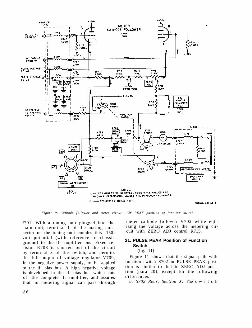
Figure 9. Cathode fol lower and meter circuit , CW PEAK posit ion of function switch.
J701. With a tuning unit plugged into themain unit, terminal 1 of the mating con-nector on the tuning unit couples this -150-volt potential (with reference to chassisground) to the if. amplifier bus. Fixed re-sistor R708 is shorted out of the circuitby terminal 3 of the switch, and permitsthe full output of voltage regulator V709,in the negative power supply, to be appliedto the if. bias bus. A high negative voltageis developed in the if. bias bus which cutsoff the complete if. amplifier, and assuresthat no metering signal can pass through
meter cathode follower V702 while eqti-izing the voltage across the metering cir-cuit with ZERO ADJ control R715.
21. PULSE PEAK Position of FunctionSwitch
(fig. 11)Figure 11 shows that the signal path with
function switch S702 in PULSE PEAK posi-tion is similar to that in ZERO ADJ posi-tion (para 20), except for the followingdifferences:
a. S702 Rear, Section X. The s w i t c h
2 6
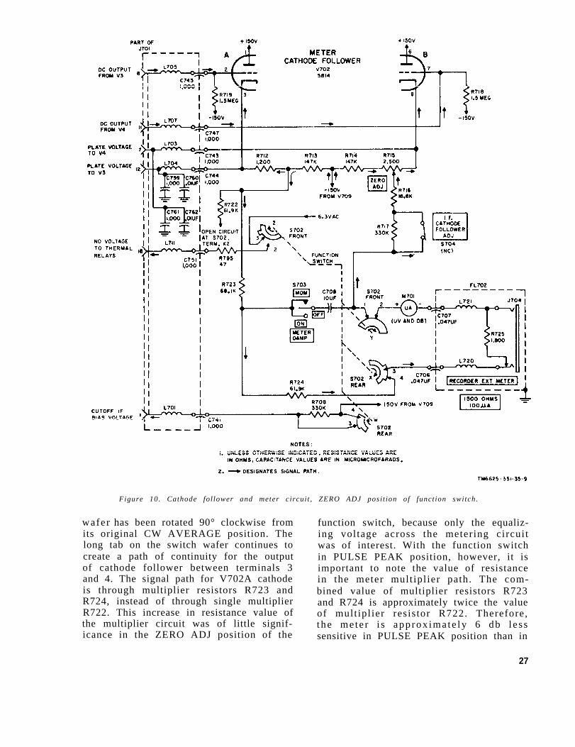
wafer
Figure 10. Cathode fol lower and meter circuit , ZERO ADJ posit ion of function switch.
has been rotated 90° clockwise from function switch, because only the equaliz-its original CW AVERAGE position. Thelong tab on the switch wafer continues tocreate a path of continuity for the outputof cathode follower between terminals 3and 4. The signal path for V702A cathodeis through multiplier resistors R723 andR724, instead of through single multiplierR722. This increase in resistance value ofthe multiplier circuit was of little signif-icance in the ZERO ADJ position of the
ing voltage across the metering circuitwas of interest. With the function switchin PULSE PEAK position, however, it isimportant to note the value of resistancein the meter mult ipl ier path. The com-bined value of multiplier resistors R723and R724 is approximately twice the valueof mult ipl ier resistor R722. Therefore,the me te r i s approx imate ly 6 db l e s ssensitive in PULSE PEAK position than in
27
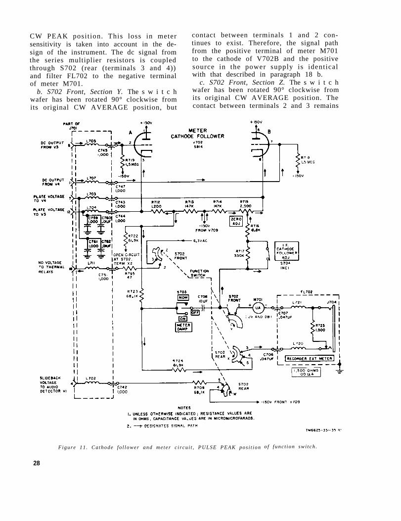
CW PEAK posit ion. This loss in metersensitivity is taken into account in the de-sign of the instrument. The dc signal fromthe series multiplier resistors is coupledthrough S702 (rear (terminals 3 and 4))and filter FL702 to the negative terminalof meter M701.
b. S702 Front, Section Y. The s w i t c hwafer has been rotated 90° clockwise fromits original CW AVERAGE position, but
contact between terminals 1 and 2 con-tinues to exist. Therefore, the signal pathfrom the positive terminal of meter M701to the cathode of V702B and the positivesource in the power supply is identicalwith that described in paragraph 18 b.
c. S702 Front, Section Z. The s w i t c hwafer has been rotated 90° clockwise fromits original CW AVERAGE position. Thecontact between terminals 2 and 3 remains
Figure 11 . Ca thode f o l l ower and me te r c i r cu i t , PULSE PEAK pos i t i on o f f u n c t i o n s w i t c h .
28
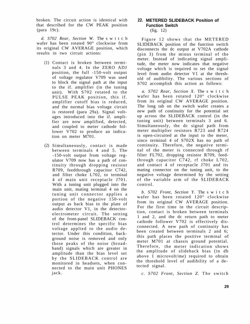
broken. The circuit action is identical withthat described for the CW PEAK position(para 19c).
d. S702 Rear, Section W. The s w i t c hwafer has been rotated 90° clockwise fromits original CW AVERAGE position, whichresults in two circuit actions:
(1)
(2)
Contact is broken between termi-nals 3 and 4. In the ZERO ADJposition, the full -150-volt outputof voltage regulator V709 was usedto block the signal path at the inputto the if. amplifier (in the tuningunit). With S702 rotated to thePULSE PEAK pos i t ion , th i s i f .amplif ier cutoff bias is reduced,and the normal bias voltage circuitis restored (para 29a). Signal volt-ages introduced into the if. ampli-fier are now amplified, detected,and coupled to meter cathode fol-lower V702 to produce an indica-tion on meter M701.
Simultaneously, contact is madebetween terminals 4 and 5. The-150-volt output from voltage reg-ulator V709 now has a path of con-t inui ty through dropping resis torR709, feedthrough capacitor C742,and filter choke L702, to terminal4 of main unit receptacle J701.With a tuning unit plugged into themain unit, mating terminal 4 on thetun ing un i t connec to r app l i e s aport ion of the negative 150-voltoutput as back bias to the plate ofaudio detector V1, in the detector-electrometer circuit . The set t ingof the front-panel SLIDEBACK con-trol determines the specific biasvoltage applied to the audio de-tector. Under this condition, back-ground noise is removed and onlythose peaks of the noise (broad-band) signals which are greater inamplitude than the bias level setby the SLIDEBACK cont ro l a remonitored in headsets, when con-nected to the main unit PHONESjack.
22. METERED SLIDEBACK Position ofFunction Switch
(fig. 12)
F igure 12 shows tha t the METEREDSLIDEBACK position of the function switchdisconnects the dc output at V702A cathode(pin 3) from the minus terminal of themeter. Instead of indicating signal ampli-tude, the meter now indicates that negativevoltage which is required to set the signallevel from audio detector V1 at the thresh-old of audibility. The various sections ofS702 accomplish this action as follows:
a. S702 Rear, Section X. The s w i t c hwafer has been rotated 120° clockwisefrom its original CW AVERAGE position.The long tab on the switch wafer creates anew path of continuity for the potential setup across the SLIDEBACK control (in thetuning unit) between terminals 3 and 6.Simultaneously, the dc signal path frommeter multiplier resistors R723 and R724is open-circuited at the input to the meter,since terminal 4 of S702X has no path ofcontinuity. Therefore, the negative termi-nal of the meter is connected through rffilter FL702, dropping resistor R709, feed-through capacitor C742, rf choke L702,and contact 4 of receptacle J701 and itsmating connector on the tuning unit, to thenegative voltage determined by the settingof the variable arm of the SLIDEBACKcontrol .
b. S702 Front, Section Y. The s w i t c hwafer has been rotated 120° clockwisefrom its original CW AVERAGE position.For the first time in the circuit descrip-tion, contact is broken between terminals1 and 2, and the dc return path to metercathode follower V702 is effectively dis-connected. A new path of continuity hasbeen created between terminals 2 and 6;this path places the positive terminal ofmeter M701 at chassis ground potential.Therefore , the me te r ind ica t ion showsthe ampli tude of s l ideback bias ( in dbabove 1 microvolt/me) required to obtainthe threshold level of audibility of a de-tected signal.
c. S702 Front, Section Z. T h e s w i t c h
29
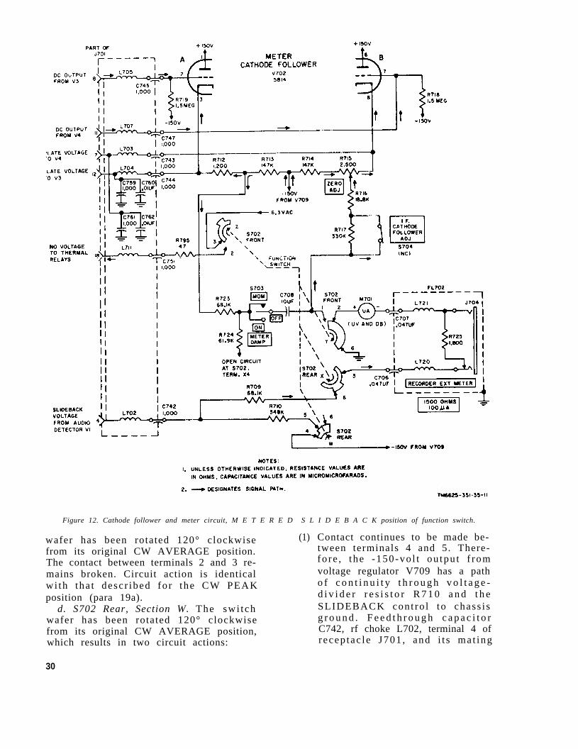
Figure 12. Cathode follower and meter circuit, M E T E R E D S L I D E B A C K position of function switch.
Contact continues to be made be-tween terminals 4 and 5. There-fo re , t he -150-vo l t ou tpu t f romvoltage regulator V709 has a patho f c o n t i n u i t y t h r o u g h v o l t a g e -d i v i d e r r e s i s t o r R 7 1 0 a n d t h eSLIDEBACK cont ro l to chass i sg r o u n d . F e e d t h r o u g h c a p a c i t o rC742, rf choke L702, terminal 4 ofrecep tac le J701 , and i t s ma t ing
wafer has been rotated 120° clockwisefrom its original CW AVERAGE position.The contact between terminals 2 and 3 re-mains broken. Circuit action is identicalwi th tha t desc r ibed fo r the CW PEAKposition (para 19a).
d. S702 Rear, Section W. The swi tchwafer has been rotated 120° clockwisefrom its original CW AVERAGE position,which results in two circuit actions:
(1)
30
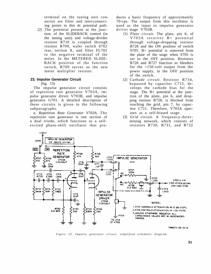
(2)
terminal on the tuning uni t con-nector are filter and interconnect-ing points in this dc potential path.The potential present at the junc-tion. of the SLIDEBACK control (inthe tuning unit) and voltage-dividerresistor R710 is coupled throughresistor R709, wafer switch S702rear, section X, and filter FL702to the nega t ive t e rmina l o f themeter. In the METERED SLIDE-BACK pos i t ion o f the func t ionswitch, R709 serves as the newmeter mult ipl ier resistor .
23. Impulse Generator Circuit(fig. 13)
The impulse generator circuit consistsof repeti t ion rate generator V703A, im-pulse generator driver V703B, and impulsegenerator G701. A detailed description ofthese circui ts is given in the fol lowingsubparagraphs.
a. Repetition Rate Generator V703A. T h erepetition rate generator is one section ofa dual triode, which functions as a self-exci ted phase-shif t osci l lator that pro-
duces a basic frequency of approximately70-cps. The output from this oscillator isused as the input to impulse generatord r i v e r
(1)
(2)
(3)
stage V703B.Plate circuit. The plate, pin 6, ofV 7 0 3 A r e c e i v e s B + p o t e n t i a lthrough voltage-dropping resistorR728 and the ON position of switchS705. B+ potential is removed fromthe plate of the stage when S705 isset to the OFF position. ResistorsR726 and R727 function as bleedersfor the +150-volt output from thepower supply, in the OFF positionof the switch.Cathode circuit . Res i s to r R734 ,bypassed by capacitor C715, de-velops the cathode bias for thestage. The B+ potential at the junc-tion of the plate, pin 6, and drop-ping resistor R728, is blocked fromreaching the grid, pin 7, by capac-itor C711. Therefore, V703A oper-ates as a self-biased stage.Grid circuit. A f requency-de te r -mining network, which consists ofresistors R730, R731, and R732
F i g u r e 1 3 . I m p u l s e g e n e r a t o r c i r c u i t , s i m p l i f i e d s c h e m a t i c d i a g r a m .
31
(4)
(in series with R734 to ground) andcapacitors C712, C713, and C714,is connected in the grid-to-cathodecircuit. Resistor R733 functions asthe grid return.Dynamic circuit description. W i t hS705 in its ON position, regener-ative voltage is coupled from theplate, pin 6, of V703A to the grid,pin 7, through capacitor C711 andt h e f r e q u e n c y - d e t e r m i n i n g n e t -work. The values of the frequency-determining elements are chosenso that the regenerat ive voltagewill be in phase with the grid volt-age at approximately 70 cycles.The oscillatory output at the plate,pin 6, is coupled through capacitorC716 to the input of impulse gen-erator driver V703B.
b . I m p u l s e G e n e r a t o r D r i v e r S t a g eV 7 0 3 B . This sect ion of the dual t r iodeserves as a driver for the coil of impulsegenerator G701 and as a power amplifier.
(1)
(2)
(3)
(4)
Plate circuit. The plate, pin 1, ofV 7 0 3 B r e c e i v e s B + p o t e n t i a lthrough the solenoid coil of G701and v 01 t a g e-dropping resistorR729, with IMPULSE GENERATORDB ABOVE 1 µV/MC switch S705in the ON position.
Cathode circuit. The voltage dropacross cathode resistor R736, atpin 3 of the tube, develops cathodeb ias .
Grid circuit. High value resis torR735, connected between pin 2 ofthe tube and chassis ground, is thegrid return.
Dynamic circuit description. T h e70-cps voltage from V703A is ap-plied to the control grid, pin 2, ofV703B. The solenoid coil of im-pulse generator G701, shunted bycapacitor C717, forms the plateload. Capacitor C718 and resistorR729 form a plate decoupling net-work. Feedthrough c a p a c i t o r sC721 and C722 bypass transientsdeveloped by the impulse generatorm e r c u r y switch contacts. The
changes in current through the coiloperates a mercury switch withinG701, which generates the 70-cpscalibrating voltage by charging andd i scha rg ing a l eng th o f coax ia lcable that functions as a delay line.
c. Impulse Generator G701. This a s -sembly consists of a coil (b above) whichsur rounds a mercury swi tch , a coax ia ldelay line in series with current-limitingres i s to r R738 , and d i scha rge pa th r e -s i s t o rbelow.
(1)
(2)
(3)
R737. Circuit action is described
The coil surrounding the mercuryswitch is part of the plate load ofi m p u l s e g e n e r a t o r d r i v e r s t a g eV703B. The 70-cps voltage devel-oped across the coil operates themoving contact at a 70-cps rate.With the contact at i ts normallyopen (NO) posit ion, the coaxialdelay l ine is connected throughcurrent-limiting resistor R738 andfeedthrough capacitor C723 to aB+ voltage determined by the set-tings of the series-connected im-pulse generator step at tenuatorsS707 and S708. This B+ voltage canbe as high as 450 volts, positiveor negative with respect to chassisground, depending on the positionof c h ass is control POLARITYswitch S709 (fig. 6).With the contact at i ts normallyclosed (NC) position, the coaxialdelay line is discharged to groundthrough resistor R737. The ????-sient discharge of the dc voltageon the delay line produces a broad-band signal whose frequency spec-trum is f lat , within one-half db,from 150 kc to 1,000 mc. Thiss p e c t r u m c o r r e s p o n d s w i t h t h efrequency coverage of the test setand c rea tes a usab le source o fcalibrating voltage which requiresno tuning of circuit elements.The t r ans ien t d i scha rge o f thecoaxial delay l ine is de-coupledthrough output connector P709 toinput jack J713 on coaxial relayK702 (fig. 14).
32
24. Coaxial Relays and Attenuators(fig. 14)
Figure 14 shows that a network of coaxialrelays and at tenuators are connected tothe rf signal input and to the impulse gen-erator output signal paths. The directionof signal flow depends on the setting ofcal ibrat ion switch S706. The fol lowingsubparagraphs ana lyze the c i r cu i t w i thS706 in the SERIES CAL & OPERATEposition (a below); then with S706 in theSHUNT CAL position (b below).
a. SERIES CAL & OPERATE Position.Two signal paths are provided by coaxialrelays K701 and K702.
(1) Rf s ignal path. The rf signal isappl ied to SIGNAL INPUT jackJ705 and i s conduc ted th roughadapter CP701 to input jack J707on coaxial relay K701. Setting cal-ibration switch S706 in the SERIESCAL & OPERATE position createsa path of continuity for the +6-voltoutput of the power supply throughthe coil of relay K701 and current-l imit ing resis tors R739-R740 tochassis ground. With relay K701energized, the movable arm on thelower set of contacts connects theincoming rf signal applied at jackJ707 on relay K701 to jack J709.The movable arm on the upper setof contacts grounds the output endof a 20-db fixed attenuator AT701,effect ively removing i t from thecircuit. The rf signal available atoutput jack J709 on the coaxialrelay is applied through plug P703,cab le a s sembly W701 , and p lugP704 to coaxial jack J718 on theinput side of the turret-type rotaryswitch on signal attenuator AT702.When the SIGNAL ATTENUATORdb control is rotated to the 0 CWONLY position (fig. 14), a 10-dbresistive T-pad attenuator networkof coaxial structure is inserted inthe signal path. The attenuated rfsignal, available at the output endof the coaxial structure, is pickedup by the output side of the turret-type rotary switch and is coupled
(2)
through coaxial jack J719 and right-angle adapter CP705. Mating plugP712 conducts the at tenuated rfsignal through a length of coaxialcable to terminal A2 of main unitmultipin connector J701. The cor-re spond ing t e rmina l A2 on themating plug (at the rear of eachtuning unit) couples the signal to therf tuner section of the tuning unitin use.
Note: When the SIGNAL ATTENUATORDB control i s ro ta ted to the 0 SUBSTONLY position, a straight-through con-ductor coaxial structure is inserted in thesignal path and no attenuation is intro-duced. With this control rotated to the 20,40, 60, and 80 positions, a 10-, 20-, 40-,or 60- db T- pad coaxial structure is re-spectively inserted in the rf signal path.The remaining part of the front-panel des-ignated amount of signal amplitude reduc-tion is obtained by the insertion of 10 or20 db additional attenuation in the if. sig-nal path (para 12b).
Impulsegenerator signal path. T h eoutput of impulse generator G701is coupled through plug P709 andmating jack J713 on coaxial relayK702. The coil of relay K702 isd e e n e r g i z e d when calibrationswitch S706 is set to the positionshown in figure 14. Therefore, themovable arm on the lower set ofcontacts provides a path of con-tinuity through adapter CP704 tofront-panel IMPULSE OUTPUTjack J717. The movable arm on theupper set of contacts grounds theinput end of 20-db fixed attenuatorAT701 , e f fec t ive ly removing i tfrom the circuit. When the discone,loop, or vert ical antenna is con-nected to the main unit, one of thep a i r o f r f c a b l e s i n E l e c t r i c a lC a b l e Assembly Set MX-3410/URM-85 mates with the output ofthe impulse generator at IMPULSEOUTPUT jack J717. Each of thesethree antennas, with the use of theseries method of calibration (fig.3), houses a self-contained 20-dbattenuator .
b. SHUNT CAL Position. T h e circuitconditions with calibration switch S706 in
33
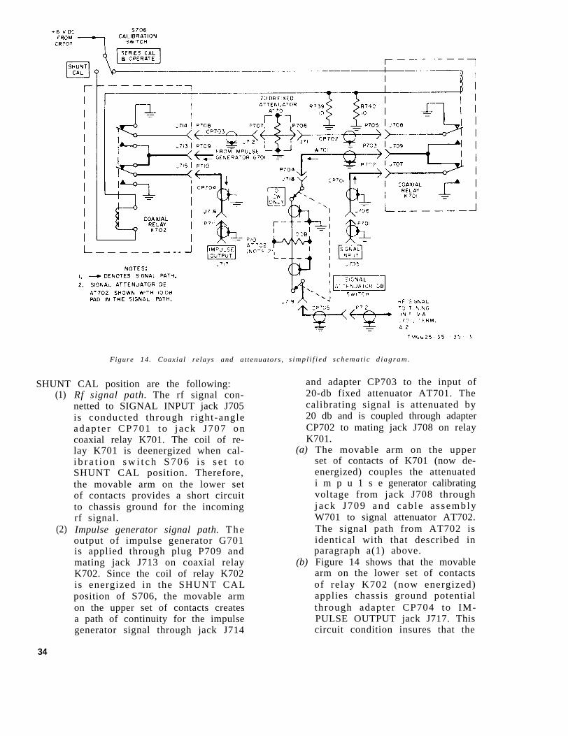
Figure 14. Coaxial relays and at tenuators, s i m p l i f i e d s c h e m a t i c d i a g r a m .
SHUNT CAL position are the following: and adapter CP703 to the input of(1)
(2)
Rf signal path. The rf signal con- 20-db fixed attenuator AT701. Thenetted to SIGNAL INPUT jack J705 calibrating signal is attenuated byis conducted through r ight-angle 20 db and is coupled through adapteradap te r CP701 to j ack J707 on CP702 to mating jack J708 on relaycoaxial relay K701. The coil of re- K701.lay K701 is deenergized when cal- (a)i b r a t i o n s w i t c h S 7 0 6 i s s e t t oSHUNT CAL position. Therefore,the movable arm on the lower setof contacts provides a short circuitto chassis ground for the incomingrf signal.Impulse generator signal path. T h eoutput of impulse generator G701is applied through plug P709 andmating jack J713 on coaxial relay (b)K702. Since the coil of relay K702is energized in the SHUNT CALposition of S706, the movable armon the upper set of contacts createsa path of continuity for the impulsegenerator signal through jack J714
The movable arm on the upperset of contacts of K701 (now de-energized) couples the attenuatedi m p u 1 s e generator calibratingvoltage from jack J708 throughjack J709 and cab le a s semblyW701 to signal attenuator AT702.The signal path from AT702 isidentical with that described inparagraph a(1) above.Figure 14 shows that the movablearm on the lower set of contactsof relay K702 (now energized)applies chassis ground potentialthrough adapter CP704 to IM-PULSE OUTPUT jack J717. Thiscircuit condition insures that the
34
calibrating signal path cannot be which may be present at the front-d i s tu rbed by any r f po ten t i a l panel IMPULSE OUTPUT jack.
Section Ill. THEORY OF TUNING UNIT 1
25. Block Diagram of Tuning Unit 1(fig. 15)
The block diagram for tuning unit 1 isshown in figure 15. For complete circuitdetai ls , refer to the schematic diagram,figure 99.
a. Six-Position Turret Tuner. The six-position turret tuner receives the rf signalfrom the main unit, and provides appro-priate tuned circuits for any of the six rfbands selected by MEGACYCLES bandswitch S1. The rf signal is then coupledto the rf amplifier.
b. Rf Amplifier Stage, V1. The rf am-plifier stage, V1, amplifies the signal andcouples it to mixer stage V2. The front-panel TUNING control tracks the rf ampli-fier and mix e r tuned circuits with theoutput of the oscillator.
c. Oscil lator, V3. Osci l l a to r V3 gen-erates a s ignal which is 455 kc higherthan the incoming rf signal for bands 1and 3 (para 26), or 1,600 kc higher thanthe incoming rf signal for bands 2, 4, 5,and 6. This signal is injected into mixerstage V2.
d . Mixer S tage V2 . M i x e r s t a g e V 2heterodynes the incoming rf signal fromrf amplifier with the oscillator frequency,and produces an output difference fre-quency. This difference frequency, whichmay be either 455 kc or 1,600 kc, depend-ing on the band selected by the setting ofthe MEGACYCLES band switch, is coupledto the if. input selector.
e. If. Input Selector. The if. input se-lector allows for automatic relay-operatedselection of either the 455-kc or the 1,600kc output from the mixer stage. The propersignal path for the selected if. signal iscompleted together with a second relayhoused in if. step attenuator AT1.
f. If. Step Attenuator AT1. If. step at-tenuator AT1 is a ladder network whichprovides an inherent 6-db loss in the sig-nal path, before the signal enters the it.
g. 1,600-Kc If. Amplifier. The 1,600-kc if. amplifier consists of four cascadeddouble-tuned if. amplifier stages: V4, V5,V6, and V7. These stages provide addi-tional gain and selectivity for the 1,600-kcif. signal. To vary the signal amplification,a front-panel GAIN control is provided.
h. 455-Kc If. Amplifier. The 455-kc if .amplifier is similar to the 1,600 kc, ex-cept that its center operating frequency is455 kc, instead of 1,600 kc. It also has fourseparate stages: V8, V9, V10, and V1l.The front-panel GAIN control, which variesthe signal amplification, is common withthe 1,600-kc if. amplifier.
i . I f . Output Selector. The i f . ou tpu tselector is a relay-operated switch whichallows the output from the if. amplifier inuse to be coup led to the de tec to r andelectrometer assembly, Al. Selection ofthe p roper r e l ay -ene rg iz ing vo l t age i sautomatic, depending. on the position ofthe MEGACYCLES band switch S1.
j . Detector and Electrometer AssemblyA1. The de tec to r and e lec t romete r a s -sembly receives the output from the if .amplifier and performs two main functions.First, the audio detector demodulates theif. signal and feeds the resultant outputsignal to audio amplifier V701 in the mainunit . Secondly, dual meter detectors areused in a voltage-divider network to sup-ply driving voltage to two separate elec-t r o m e t e r s t a g e s . T h e s e a r e e x t r e m e l yhigh-impedance electron tubes which faith-fully reproduce the applied input signal,with no degradation or amplification, in itsamplifier. Two additional steps of attenua-tion, 10 db or 20 db, are inserted in thesignal path by rotating SIGNAL ATTEN-UATOR DB switch S701 to its various posi-tions. In the 0 SUBST ONLY and 0 CWONLY positions of S701, 6 db attenuationis in the if . s ignal path. In the 20 DBposition, 16 db of attenuation is in the path;in the 40, 60, and 80 DB positions, 26 dbof attenuation is in the path.
35
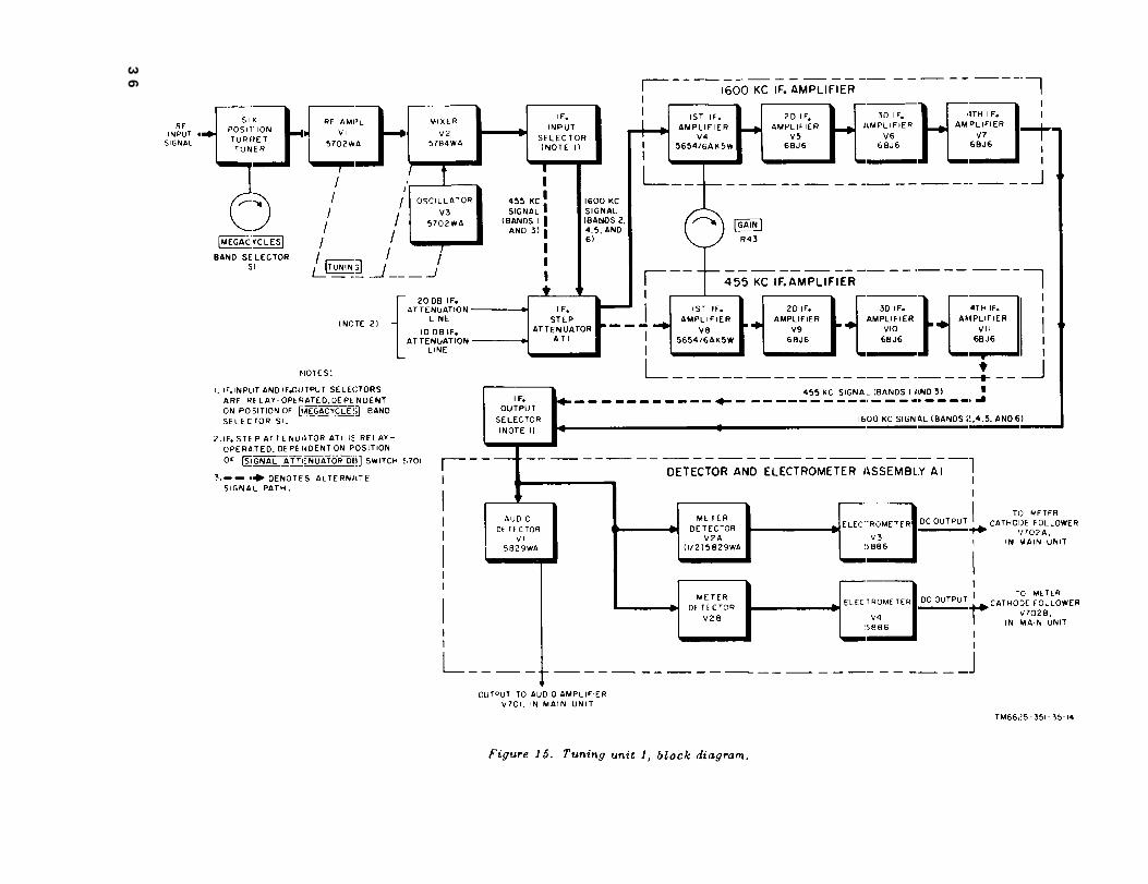
Figure 15.
36
output circuit . The electrometers supplydriving voltage to meter cathode followersV702A and V702B in the main unit.
26. Rf Tuner Section, Detailed Analysis(fig. 16)
The six-posi t ion turret tuner (f ig. 56)contains six separate phenolic segmentson which are mounted rf t ransformers,t r i m m e r s , capacitors , and load ing r e -s i s to r s fo r the s ix d i f f e ren t f r equencybands. Each tuner segment has three setsof coils and trimmers: the input grid cir-cuit of the rf amplifier, the coupling circuitfrom the plate of the rf amplifier to themixer, and the tuned circuit for the oscil-lator. Since the segments are essentiallysimilar in design, except for componentvalues and tuned frequencies, the circuitanalysis given in the following subpara-graphs is based on a detailed explanation,with MEGACYCLES band switch set toband 1 (fig. 16). The frequency bands areas follows:
Frequency cove rageI n t e r m e d i a t e
B a n d(mc)
f requency( k c )
123456
0 .15 to 0 .360 .36 to 0 .870 .87 to 2 .12.1 to 5.25 .2 to 12 .7
12.7 to 30
4551,600
4551,6001,6001,600
a. Rf Transformer Primay Circuit. T h erf signal from the main unit is fed throughconnector P1 (terminal A2) to contact 2 ofthe springfinger contacts on the rf chassis.The project ing terminal 2 on the tunersegment couples the incoming signal to theprimary of antenna transformer T4. Ter-minal 3 of the tuner segment has a path ofcontinuity to chassis ground through thewiper springfinger contacts . Therefore,terminal 3 on the tuner segment and itsmating wiper contact connect one side ofthe p r imary wind ing o f T4 to chass i sground. This rf t ransformer presents animpedance of approximately 50 ohms tothe incoming signal.
b. Rf Transformer Secondary Circuit .The secondary of transformer T4, togetherwith trimmer capacitors C8 and C9, steps
up the voltage of the desired incomingsignal. Terminal 6 of the tuner segmentand the mating wiper contact applies thesignal to the grid of rf amplifier V1. Ter-minal 5 of the tuner segment and the mat-ing wiper contact connects the low-poten-tial side of T4 secondary winding to chassisground.
c. Rf Amplif ier V1. The r f ampl i f i e r ,V1, is a pentode amplifier with tuned cir-cuits in the grid and plate circuits to pro-vide selectivity in the stage. These tunedcircuits are contained on the turret tuner,and are different for each of the six fre-quency bands. Turning MEGACYCLES bandswitch S1 connects the appropriate tunedcircuit to the rf amplifier. Capacitor C52Cis part of the three-section variable air-dielectric TUNING capacitor which servesto resonate the antenna transformer to theincoming signal frequency. Grid bias isprovided by the voltage drop across cathoderesistor R10. Capacitor C58 functions asthe bypass capac i to r . Res i s to r R9 i s ascreen-dropping resistor , with capacitorC57 serving as a screen bypass capacitor.Coils L2, L3, and L4, and capacitors C66,C67, and C68 prevent rf currents fromcirculat ing in the heater circuits of al lthree stages in the rf tuner section. Re-sistor R11, together with capacitors C56and C61, provide decoupling for the platecircuit. Resistor R12 drops the B+ voltageto a value required by the plate circuit.The amplified output of rf amplifier V1 isdeveloped across the primary of interstagetransformer T2. Terminals 9 and 10 of thetuner segment, and their mating wiper con-tacts, create a path of continuity from theplate, pin 1, of V1 through the primarywinding of T2, to decoupling resistor Rlland the power supply. The output signal isinductively coupled to the signal injectiongrid, pin 7, of mixer stage V2.
Note: Coil L1 and capacitor C59 function as a1,600-kc trap. This circuit helps to prevent un-wanted 1,600-kc s i g n a l s from appearing in the1,600-kc if. amplifler when this if. amplifier is op-erating. In band 3 (0.87 to 2.1 me), which encom-passes 1,600 kc as a frequency within its tuningrange, the trap circuit is shorted to ground. Thiscircuit arrangement enables an incoming rf signalof 1,600 kc to be received and detected in the con-ventional manner. In bands 2, 4, 5, and 6, however,the 1,600-kc if. amplifier is energized. A method
37
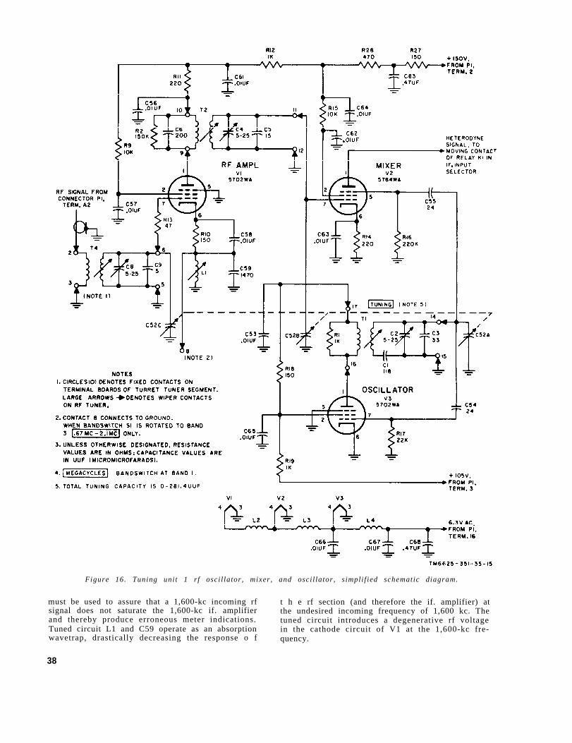
Figure 16. Tuning unit 1 rf osci l lator, mixer, and osci l lator, s impli f ied schematic diagram.
must be used to assure that a 1,600-kc incoming rf t h e rf section (and therefore the if. amplifier) atsignal does not saturate the 1,600-kc if. amplifier the undesired incoming frequency of 1,600 kc. Theand thereby produce erroneous meter indications. tuned circuit introduces a degenerative rf voltageTuned circuit L1 and C59 operate as an absorption in the cathode circuit of V1 at the 1,600-kc fre-wavetrap, drastically decreasing the response o f quency.
38
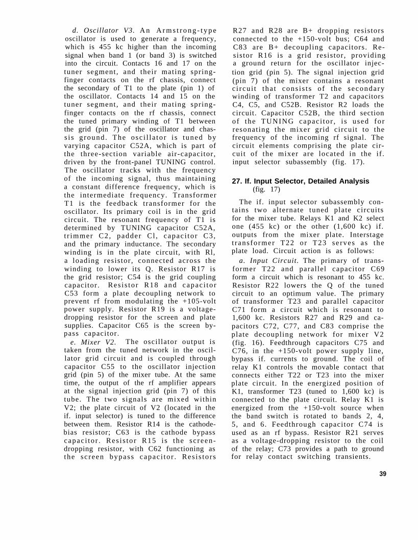
d. Oscillator V3. A n A r m s t r o n g - t y p eoscillator is used to generate a frequency,which is 455 kc higher than the incomingsignal when band 1 (or band 3) is switchedinto the circuit. Contacts 16 and 17 on thetuner segment, and their mating spring-finger contacts on the rf chassis, connectthe secondary of T1 to the plate (pin 1) ofthe oscillator. Contacts 14 and 15 on thetuner segment, and their mating spring-finger contacts on the rf chassis, connectthe tuned primary winding of T1 betweenthe grid (pin 7) of the oscillator and chas-s i s g round . The osc i l l a to r i s t uned byvarying capacitor C52A, which is part ofthe three-section variable air-capacitor ,driven by the front-panel TUNING control.The oscillator tracks with the frequencyof the incoming signal, thus maintaininga constant difference frequency, which isthe intermediate frequency. TransformerT1 is the feedback transformer for theoscillator. Its primary coil is in the gridcircuit. The resonant frequency of T1 isdetermined by TUNING capacitor C52A,t r immer C2 , padder Cl , capac i to r C3 ,and the primary inductance. The secondarywinding is in the plate circuit, with Rl,a loading resistor , connected across thewinding to lower its Q. Resistor R17 isthe grid resistor; C54 is the grid couplingcapacitor . Res i s to r R18 and capac i to rC53 form a plate decoupling network toprevent rf from modulating the +105-voltpower supply. Resistor R19 is a voltage-dropping resistor for the screen and platesupplies. Capacitor C65 is the screen by-pass capacitor .
e. Mixer V2. The oscil lator output istaken from the tuned network in the oscil-lator grid circuit and is coupled throughcapacitor C55 to the oscillator injectiongrid (pin 5) of the mixer tube. At the sametime, the output of the rf amplifier appearsat the signal injection grid (pin 7) of thistube. The two signals are mixed withinV2; the plate circuit of V2 (located in theif. input selector) is tuned to the differencebetween them. Resistor R14 is the cathode-bias resistor; C63 is the cathode bypasscapac i to r . Res i s to r R15 i s the sc reen-dropping resistor, with C62 functioning asthe sc reen bypass capac i to r . Res i s to r s
R27 and R28 are B+ dropping resistorsconnected to the +150-volt bus; C64 andC83 are B+ decoupling capacitors. Re-sis tor R16 is a grid resis tor , providinga ground return for the oscillator injec-tion grid (pin 5). The signal injection grid(pin 7) of the mixer contains a resonantc i r cu i t t ha t cons i s t s o f the secondarywinding of transformer T2 and capacitorsC4, C5, and C52B. Resistor R2 loads thecircuit. Capacitor C52B, the third sectionof the TUNING capac i to r , i s used fo rresonating the mixer grid circui t to thefrequency of the incoming rf signal. Thecircuit elements comprising the plate cir-cuit of the mixer are located in the if .input selector subassembly (fig. 17).
27. If. Input Selector, Detailed Analysis(fig. 17)
The if. input selector subassembly con-tains two alternate tuned plate circuitsfor the mixer tube. Relays K1 and K2 selectone (455 kc) or the other (1,600 kc) if.outputs from the mixer plate. Interstaget rans fo rmer T22 o r T23 se rves as theplate load. Circuit action is as follows:
a. Input Circuit. The primary of trans-former T22 and paral lel capacitor C69form a circuit which is resonant to 455 kc.Resistor R22 lowers the Q of the tunedcircuit to an optimum value. The primaryof transformer T23 and parallel capacitorC71 form a circuit which is resonant to1,600 kc. Resistors R27 and R29 and ca-pacitors C72, C77, and C83 comprise theplate decoupling network for mixer V2(fig. 16). Feedthrough capacitors C75 andC76, in the +150-volt power supply line,bypass if. currents to ground. The coil ofrelay K1 controls the movable contact thatconnects either T22 or T23 into the mixerplate circuit. In the energized position ofK1, transformer T23 (tuned to 1,600 kc) isconnected to the plate circuit. Relay K1 isenergized from the +150-volt source whenthe band switch is rotated to bands 2, 4,5, and 6. Feedthrough capacitor C74 isused as an rf bypass. Resistor R21 servesas a voltage-dropping resistor to the coilof the relay; C73 provides a path to groundfor relay contact switching transients.
39
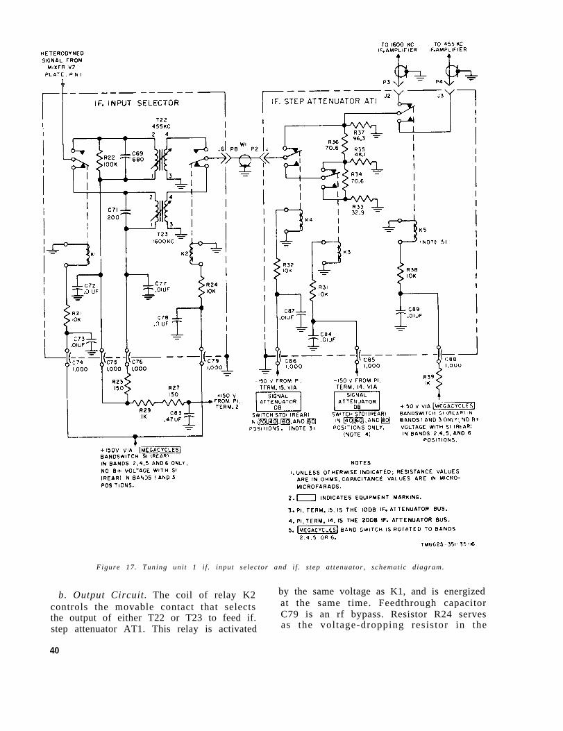
Figure 17. Tuning unit 1 i f . input selector and i f . s tep at tenuator, schematic diagram.
b. Output Circuit. The coil of relay K2 by the same voltage as K1, and is energized
controls the movable contact that selects at the same time. Feedthrough capacitor
the output of either T22 or T23 to feed if. C79 is an rf bypass. Resistor R24 serves
step attenuator AT1. This relay is activated as the vol tage-dropping resis tor in the
40
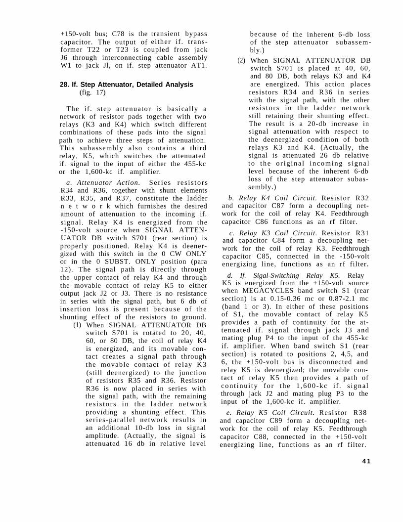
+150-volt bus; C78 is thecapacitor. The output of
transient bypasseither if . t rans-
former T22 or T23 is coupled from jackJ6 through interconnecting cable assemblyW1 to jack Jl, on if. step attenuator AT1.
28. If. Step Attenuator, Detailed Analysis(fig. 17)
The if . s tep at tenuator is basical ly anetwork of resistor pads together with tworelays (K3 and K4) which switch differentcombinations of these pads into the signalpath to achieve three steps of attenuation.This subassembly also contains a thirdrelay, K5, which switches the attenuatedif. signal to the input of either the 455-kcor the 1,600-kc if. amplifier.
a. Attenuator Action. Ser ies r e s i s to r sR34 and R36, together with shunt elementsR33, R35, and R37, constitute the laddern e t w o r k which furnishes the desiredamount of attenuation to the incoming if.s ignal . Relay K4 is energized from the-150-volt source when SIGNAL ATTEN-UATOR DB switch S701 (rear section) isproperly positioned. Relay K4 is deener-gized with this switch in the 0 CW ONLYor in the 0 SUBST. ONLY position (para12). The signal path is directly throughthe upper contact of relay K4 and throughthe movable contact of relay K5 to eitheroutput jack J2 or J3. There is no resistancein series with the signal path, but 6 db ofinsert ion loss is present because of theshunting effect of the resistors to ground.
(1) When SIGNAL ATTENUATOR DBswitch S701 is rotated to 20, 40,60, or 80 DB, the coil of relay K4is energized, and its movable con-tact creates a signal path throughthe movable contact of relay K3(still deenergized) to the junctionof resistors R35 and R36. ResistorR36 is now placed in series withthe signal path, with the remainingres i s to r s in the l adder ne tworkproviding a shunting effect. Thisseries-paral lel network results inan additional 10-db loss in signalamplitude. (Actually, the signal isattenuated 16 db in relative level
(2)
because ofof the stepbly.)
the inherent 6-db lossat tenuator subassem-
When SIGNAL ATTENUATOR DBswitch S701 is placed at 40, 60,and 80 DB, both relays K3 and K4are energized. This action placesresistors R34 and R36 in serieswith the signal path, with the otherres i s to r s in the l adder ne tworkstill retaining their shunting effect.The result is a 20-db increase insignal attenuation with respect tothe deenergized condition of bothrelays K3 and K4. (Actually, thesignal is attenuated 26 db relativeto the o r ig ina l i ncoming s igna llevel because of the inherent 6-dbloss of the step attenuator subas-sembly.)
b. Relay K4 Coil Circuit. Resistor R32and capacitor C87 form a decoupling net-work for the coil of relay K4. Feedthroughcapacitor C86 functions as an rf filter.
c. Relay K3 Coil Circuit. Resistor R31and capacitor C84 form a decoupling net-work for the coil of relay K3. Feedthroughcapacitor C85, connected in the -150-voltenergizing line, functions as an rf filter.
d. If. Sigal-Switching Relay K5. RelayK5 is energized from the +150-volt sourcewhen MEGACYCLES band switch S1 (rearsection) is at 0.15-0.36 mc or 0.87-2.1 mc(band 1 or 3). In either of these positionsof S1, the movable contact of relay K5provides a path of continuity for the at-tenuated if . s ignal through jack J3 andmating plug P4 to the input of the 455-kcif. amplifier. When band switch S1 (rearsection) is rotated to positions 2, 4,5, and6, the +150-volt bus is disconnected andrelay K5 is deenergized; the movable con-tact of relay K5 then provides a path ofcon t inu i ty fo r the 1 ,600-kc i f . s igna lthrough jack J2 and mating plug P3 to theinput of the 1,600-kc if. amplifier.
e. Relay K5 Coil Circuit. Resistor R38and capacitor C89 form a decoupling net-work for the coil of relay K5. Feedthroughcapacitor C88, connected in the +150-voltenergizing line, functions as an rf filter.
4 1
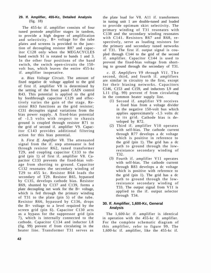
29. If. Amplifier, 455-Kc, Detailed Analysis(fig. 18)
The 455-kc if. amplifier consists of fourtuned pentode amplifier stages in tandem,to provide a high degree of amplificationand select ivi ty. B+ voltage for the tubeplates and screens is provided to the junc-tion of decoupling resistor R87 and capac-itor C128 only when the MEGACYCLESband switch S1 is rotated to bands 1 and 3.In the other four posi t ions of the bandswitch, the switch open-circuits the 150-volt bus, which leaves the entire 455-kcif. amplifier inoperative.
a. Bias Voltage Circuit. The amount offixed negative dc voltage applied to the gridof first if. amplifier V8 is determined bythe setting of the front panel GAIN controlR43. This potential is applied to the gridby feedthrough capacitor C129 and effec-t ively varies the gain of the stage. Re-sistor R63 functions as the grid resistor;Cl31 decouples signal variations from thebias power supply. A fixed-bias potentialof -1 .5 vo l t s wi th r e spec t to chass i sground is coupled through resistor R71 tothe grid of second if. amplifier V9. Capac-i tor C143 provides addit ional f i l ter ingaction for this bias potential.
b. First If. Amplifier V8. The at tenuatedsignal from the if. step attenuator is fedthrough resistor R62, tuned transformerT29, and coupling capacitor C133 to thegrid (pin 1) of first if. amplifier V8. Ca-pacitor C133 prevents the fixed-bias volt-age from short ing to ground. CapacitorC132 resonates the secondary winding ofT29 to 455 kc. Resistor R64 loads thesecondary of T29. Resistor R65, bypassedby C135, develops cathode bias. ResistorR69, shunted by C137 and C139, forms aplate decoupling net work for the B+ voltage,which is fed through the primary windingof T31 to the plate (pin 5) of the tube.Resistor R66, bypassed by C136, dropsthe B+ voltage to a level required by thescreen grid (pin 6). Capacitor C130 actsas a bypass for the suppressor grid (pin7), which is internally connected to thecathode. Capacitor C134 and inductor L8(fig. 99) prevent rf from circulating in theheater l ine. Transformer T31 serves as
42
the plate load for V8. A11 if. transformersin tuning unit 1 are double-tuned and loadedto provide optimum skirt selectivity. Theprimary winding of T31 resonates withC138 and the secondary winding resonateswith C141. Resistors R67 and R68, re-spectively, serve as loading resistors forthe primary and secondary tuned networksof T31. The first if. output signal is cou-pled through C144 to the grid of the secondif. amplifier. Capacitor C144 is used toprevent the fixed-bias voltage from short-ing to ground through the secondary of T31.
c. If. Amplifiers V9 through V11. T h esecond, third, and fourth if . amplif iersare similar in circuitry to the first, exceptfo r the i r b ia s ing ne tworks . Capac i to r sC146, C153 and C159, and inductors L9 andL11 (fig. 99) prevent rf from circulatingin the common heater supply line.
(1)
(2)
(3)
Second if . amplifier V9 receivesa fixed bias from a voltage dividerin the negative 150-volt bus whichapplies approximately -1.5 volts dcto i t s g r id . Cathode bias is de-veloped by R72.Third if . amplifier V10 operateswith self-bias. The cathode currentthrough R77 develops a dc voltagewhich is positive in reference tothe grid (pin 1). The grid has a dcpath to ground through the low-resistance secondary winding ofT32.Fourth if. amplifier V11 operateswith self-bias. The cathode currentthrough R83 develops a dc voltagewhich is positive with reference tothe grid (pin 1). The grid has a dcpath to ground through the low-resistance secondary winding ofT33. The output signal from V11 isapplied to the if. output selectorthrough T34.
30. If. Amplifier, 1,600-Kc, GeneralAnalysis
The 1,600-kc if. amplifier is identicalin operation with the 455-kc if. amplifier.For the complete schematic diagram ofthis amplif ier , refer to f igure 99. The1,600-kc if. amplifier, like the 455-kc if.
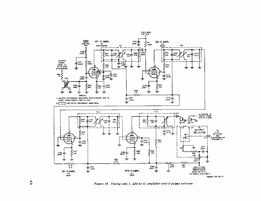
43
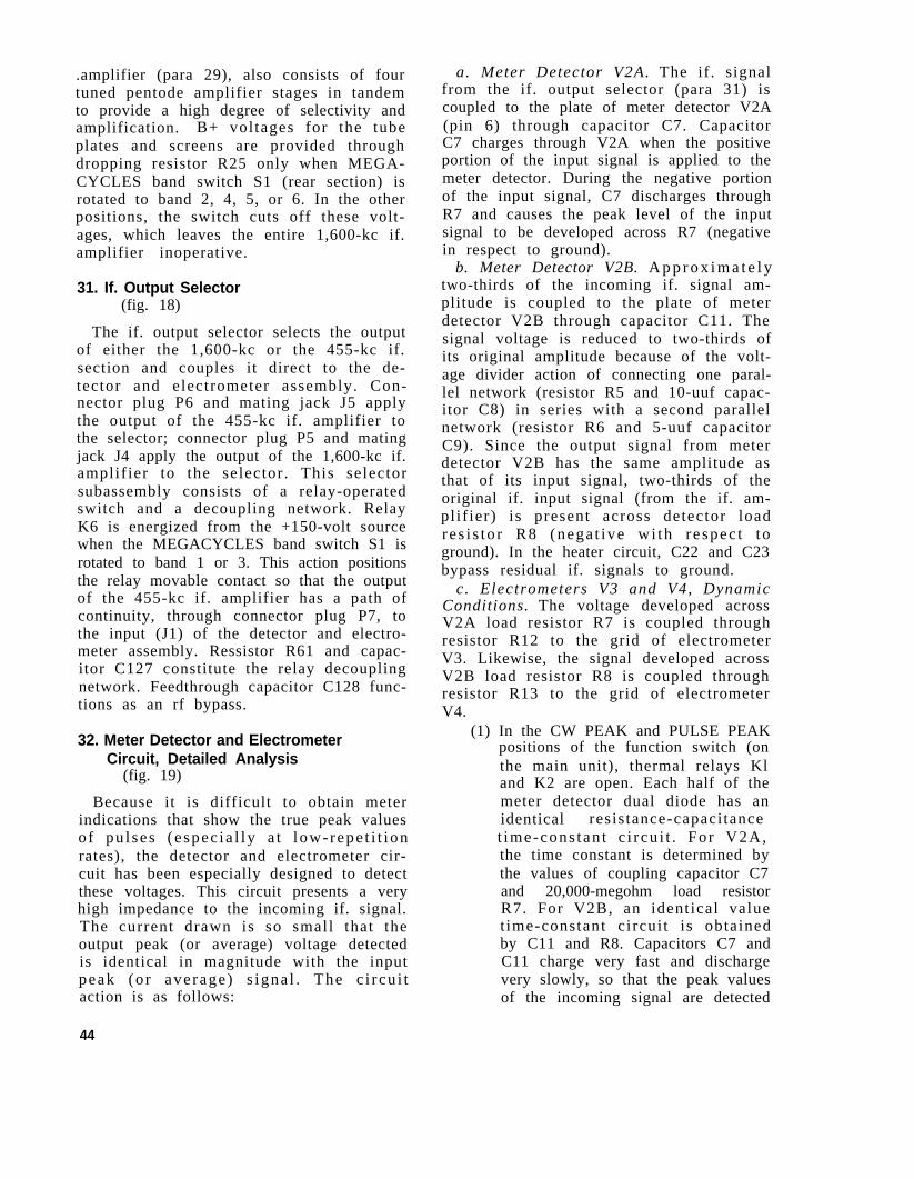
.amplifier (para 29), also consists of fourtuned pentode amplifier stages in tandemto provide a high degree of selectivity andamplification. B+ voltages for the tubeplates and screens are provided throughdropping resistor R25 only when MEGA-CYCLES band switch S1 (rear section) isrotated to band 2, 4, 5, or 6. In the otherpositions, the switch cuts off these volt-ages, which leaves the entire 1,600-kc if.amplifier inoperative.
31. If. Output Selector(fig. 18)
The if. output selector selects the outputof either the 1,600-kc or the 455-kc if.section and couples it direct to the de-tector and electrometer assembly. Con-nector plug P6 and mating jack J5 applythe output of the 455-kc if. amplifier tothe selector; connector plug P5 and matingjack J4 apply the output of the 1,600-kc if.amplif ier to the selector . This selectorsubassembly consists of a relay-operatedswitch and a decoupling network. RelayK6 is energized from the +150-volt sourcewhen the MEGACYCLES band switch S1 isrotated to band 1 or 3. This action positionsthe relay movable contact so that the outputof the 455-kc if. amplifier has a path ofcontinuity, through connector plug P7, tothe input (J1) of the detector and electro-meter assembly. Ressistor R61 and capac-itor C127 constitute the relay decouplingnetwork. Feedthrough capacitor C128 func-tions as an rf bypass.
32. Meter Detector and ElectrometerCircuit, Detailed Analysis
(fig. 19)
Because it is difficult to obtain meterindications that show the true peak valuesof pu l ses ( e spec ia l ly a t l ow- repe t i t ionrates), the detector and electrometer cir-cuit has been especially designed to detectthese voltages. This circuit presents a veryhigh impedance to the incoming if. signal.The current drawn is so small that theoutput peak (or average) voltage detectedis identical in magnitude with the inputpeak (o r average) s igna l . The c i rcu i taction is as follows:
a. Meter Detector V2A. The if. signalfrom the if. output selector (para 31) iscoupled to the plate of meter detector V2A(pin 6) through capacitor C7. CapacitorC7 charges through V2A when the positiveportion of the input signal is applied to themeter detector. During the negative portionof the input signal, C7 discharges throughR7 and causes the peak level of the inputsignal to be developed across R7 (negativein respect to ground).
b. Meter Detector V2B. A p p r o x i m a t e l ytwo-thirds of the incoming if. signal am-plitude is coupled to the plate of meterdetector V2B through capacitor C11. Thesignal voltage is reduced to two-thirds ofits original amplitude because of the volt-age divider action of connecting one paral-lel network (resistor R5 and 10-uuf capac-itor C8) in series with a second parallelnetwork (resistor R6 and 5-uuf capacitorC9). Since the output signal from meterdetector V2B has the same amplitude asthat of its input signal, two-thirds of theoriginal if. input signal (from the if. am-plif ier) is present across detector loadres i s to r R8 (nega t ive wi th r e spec t toground). In the heater circuit, C22 and C23bypass residual if. signals to ground.
c. Electrometers V3 and V4, DynamicConditions. The voltage developed acrossV2A load resistor R7 is coupled throughresistor R12 to the grid of electrometerV3. Likewise, the signal developed acrossV2B load resistor R8 is coupled throughresistor R13 to the grid of electrometerV4.
(1) In the CW PEAK and PULSE PEAKpositions of the function switch (onthe main unit), thermal relays Kland K2 are open. Each half of themeter detector dual diode has anidentical resistance-capacitancet ime-cons tan t c i rcu i t . For V2A,the time constant is determined bythe values of coupling capacitor C7and 20,000-megohm load resistorR7. For V2B, an identical valuet ime-constant circui t is obtainedby C11 and R8. Capacitors C7 andC11 charge very fast and dischargevery slowly, so that the peak valuesof the incoming signal are detected
44
F i g u r e 1 9 . D e t e c t o r a n d e l e c t r o m e t e r a s s e m b l y , s c h e m a t i c d i a g r a m
and maintained at a high level for thecoupling to the metering circuit.In the CW AVERAGE position ofthe function switch, thermal relaysK1 and K2 close. The closing of thethermal relays is obtained by ap-plying 6.3 volts ac power throughfunction switch S702, terminal 7 ofconnec to r J2 , and d ropp ing re -sistors R14-R15 to the heaters of
t h e r m a l r e l a y s . U n d e r t h i scondit ion, the load resis tors forde tec to rs V2A and V2B are re -turned to chassis ground by themuch l o w e r resistance of the4 7 0 , 0 0 0 - o h m r e s i s t o r s , R 9 a n dR11. Because of the considerablylower value of the t ime-constantcircuit, only average values of theincoming signal are detected and
45
coupled to the metering circuit inthe main unit.
d. Electrometers 3 and V4, Circuit De-scription. Because of the very high inputimpedance of the type 5886 electrometertube, almost no grid current is drawn byV3 and V4. Resistor R12 and capacitorC13 in the grid circuit of electrometer V3serve as a filter for the detected if. signal.Capacitor C13 also functions to place thegrid of V3 at low rf potential. An identicalcircuit is used at the input to electrometerstage V4, with R13 and C16 as the if. filterelements. Capacitor C12, connected to thejunction of thermal relay heater resistorsR14 and R15, bypasses if, currents in theheater circuit of thermal relays K1 and K2to chassis ground.
(1) Electrometer V3 serves as an ex-tremely high impedance triode am-plifier. Its screen (pin 2) and itsplate (pin 1) are tied together andreceive a dc plate potential throughterminal 10 of receptacle J2 fromthe cathode of meter cathode fol-lower V702A in the main unit. Theheater circuit of V3 receives 1.2volts dc through terminals 1 and 9of J2 from a rectifier circuit in themain unit power supply and is re-turned to -150 vol ts dc throughR719. Resistor R719 serves as theelectrometer output load and thegrid return of V702A. CapacitorsC14 and C17 bypass rf currentsin the hea te r c i r cu i t t o chass i sg r o u n d and prevent modulationfeedback to the power supply. Re-sistor R16 is a balancing resistorwhich is tied across the two heaterterminals. The value of R16 is se-lected in production to counteractv a r i a t i o n s i n h e a t e r r e s i s t a n c ewhich are inherent in the manu-fac tu re o f these tubes . The de -t e c t e d signal envelope voltage(negative with respect to ground),which is identical in amplitude withthe output of meter detector V2A,is taken from the heater circuit(pin 3). This signal is a p p 1 i e dthrough terminal 9 of J2 to the
(2)metering circuit in the main unit.Electrometer V4 also functions asan extremely high input impedancetriode amplifier. Similar to elec-trometer V3, the plate (pin 1) andscreen (pin 2) are tied to the com-mon source of plate potential. ForV4, however, the source voltage isthrough terminal 4 of J2, whichconnects to the cathode of metercathode follower V702B in the mainunit. The heater circuit of V4 re-ceives 1.2 volts dc, through termi-nals 2 and 3 of J2, from a separaterectifier circuit in the main unitpower supply. Capacitors C15 andC18 bypass rf currents in the heatercircuit to chassis ground, and servethe same functions as capacitorsC14 and U17 for stage V3. Sim-ilarly, R17 is the balancing resistorfo r the hea te r c i r cu i t . For th i sstage, the detected signal envelopevoltage is one-third the amplitudeof electrometer V3, since the volt-age divider at the input to meterdetector V2 divides the incomingif. signal into a ratio of 3 to 1.This detected signal envelope volt-a g e ( n e g a t i v e w i t h r e s p e c t t oground) is taken from the heatercircuit (pin 3) and is applied throughterminal 3 of J2 to the meteringcircuit in the main unit.
e. Signal and Power Paths. Interconnec-tions from the output of the detector andelectrometer assembly to the main unitare identical in all four tuning units. Es-sentially, four components comprise theinterconnection system. These are:
(1)
(2)
(3)
(4)
A mult ipin receptacle, J2, whichis an integral nonreplaceable partof the detector and electrometerassembly.A mating multipin connector (P9for tuning unit 1) which is a sub-miniature plug-in connector thatmates receptacle J2.A wiring harness which intercon-nects the tuning unit and the de-tector and electrometer assembly.A 2 0 - p i n c o n n e c t o r w h i c h i smounted at the rear of the tuning
46
unit. This receptacle is the termi-nating point for the wiring harness.When a tuning unit is inserted intothe compartment provided in themain unit , this 20-pin connectormates the 20-pin receptacle locatedin the interior of the main unit tun-compartment.
33. Audio Detector VI(fig. 19)
Audio detector V1 is also mounted withinthe detector and electrometer assembly.The amplified if. signal, coupled throughthe if. input selector, is detected by thisstage, filtered, and fed to the main unitfor audio monitoring.
a. Input Circuit. Input connector J1 re-ceives the if. signal from the if. outputselector. Capacitor C6 couples this signalto one plate (pin 1) of the dual diode audiodetector, One diode of the audio detectoris not used, and its elements (pins 6 and 7)are connected to chassis ground.
b. Output Circuit, without S l i d e b a c kAc t ion . Posit ive al ternat ions of the in-coming signal are detected at the plate.Residual if. signal frequencies are filteredfrom the detected audio signal by twoL-section pads, which consist of resistorsR1 and R2, and capacitors C2 and C3. Thefiltered output signal is coupled throughcapacitor C1 to terminal 14 of multipinreceptacle J2 and its mating plug P9 (whentuning unit 1 is in use) for application tothe audio amplifier in the main unit. Ca-pacitors C19 and C21 bypass all rf cur-rents in the filament circuit to ground.
c. Output Circuit, with Slideback Action.The SLIDEBACK control, which is mountedon the tuning unit front panel, provides ameans of reducing the amplitude of de-
tected signals to the threshold of audibility.This circuit arrangement achieves a highdegree of discrimination between the mon-itored signal and other interfering signalsthat may be present. In the METEREDSLIDEBACK position of function switchS702, the output of the negative 150-voltpower supply is applied across SLIDE-BACK control R92 (for tuning unit 1), volt-age divider resis tor R709 (mounted onfunction switch S702), and chassis wound.
Note: For tuning unit 2, the SLIDEBACK controlis R273; for tuning unit 3, the control is R473; fortuning unit 4, the control is R587.
(1)
(2)
(3)
Depending on the position of thevar i ab le a rm of th i s con t ro l , anegative voltage within the rangef rom ze ro to approx imate ly -35vo l t s w i th r e spec t t o g round i spresent at terminal 13 of connec-tors P9 and J2.This negative voltage is coupledto two L-sec t ion f i l t e r s , whichconsist of resis tors R3 and R4,and capacitors C4 and C5, con-nected in series with the L-sectionfi l ters (R1-C1 and R2-C3) whichare tied to the plate output of theaudio detector.T h e n e g a t i v e v o l t a g e f r o m t h eSLIDEBACK control has a path ofcontinuity through R4, R3, R2, andR1 to bias the plate of audio de-tector V1. Under this condit ion,only those incoming if. signals withan amplitude that can override thenega t ive b ia s po ten t i a l a re de -tected. In slideback operation of thetest set, the SLIDEBACK controlis rotated to that setting that per-mits the operator to hear the leastaudible signal . This signal Is atthe threshold of audible sensitiviy.
Section IV. THEORY OF TUNING UNIT 2
34. Block Diagram of Tuning Unit 2 sembly which houses the two different(fig. 20) sections for covering the 20- to 220-mc
The block diagram for tuning unit 2 is frequency spectrum in two bands. These
shown in figure 20, For complete circuit are as
de ta i l s , r e fe r to the overa l l schemat ic (1)diagram (fig. 100).
a. Rf Tuner. The rf tuner is a subas-
follows:
27-mc section. With band selectorS201 set to the 20-70 mc position,f i r s t r f ampl i f i e r V201 rece ives
47
(2)
the incoming rf signal which iscoupled from the main unit throughconnector plug P202 and matingjack J201. The amplified rf signalis then applied to second rf ampli-fier V202 for further amplification.Two signals are coupled to mixerV203A; one is the amplified rf out-put of V202, the second is the outputof oscillator V203B. The oscillatorgenerates a signal that tracks 10.7mc higher than the incoming rfsignal . The mixed stage hetero-dynes the rf incoming signal withthe oscillator signal; this producesa difference frequency (10.7 mc)output that is coupled through sec-tion A of band selector S201 to theif. step attenuator.70-220-mc section. The 70-220-mc sect ion funct ions identical lywith the 20-70-mc section, exceptthat selector S201 must be set tothe higher frequency band for itsoperation. First and second rf am-p l i f i e r s V204 and V205 , mixerV206A, and oscillator V206B servethe same purpose as described in(1) above, with the oscillator alsotracking 10.7 mc above the incom-ing rf signal.
b. I f . Step Attenuator AT201. The i f .step attenuator is a ladder network which,similar to the s tep at tenuator in tuningunit 1 (para 25f) , provides an inherent6-db loss in the s ignal path before thesignal enters the if , amplif ier . Two ad-ditional steps of attenuation (each 10 db)are inserted when SIGNAL ATTENUATORDB switch S701 (in the main unit) is ro-tated to its last four clockwise positions.With S701 rotated to its 20 DB front-panelsetting, the 10-db attenuation line is en-ergized and the incoming signal is reducedin amplitude by 16 db. (This total loss isobtained by adding the 6-db inherent lossof the subassembly to the loss produced byenergizing the 10-db attenuation line.) WithS701 rotated to its 40, 60, or 80 db posi-tion, the 20-db attenuation line is energizedand the incoming s igna l i s r educed inampli tude by 26 db. (This total loss isobtained by adding the 6-db inherent loss
48
of the subassembly to the loss producedby energizing the 20-db attenuation line.)The output of the if . s tep at tenuator iscoupled to the first if. amplifier.
c. I f . Amplif ier 10.7-Mc. This c i r cu i tincludes the first through fourth if. ampli-fiers, V207 through V210, and if. cathodefollower V211. The four amplifier stagesprovide additional signal gain and selec-tivity. Each stage is tuned to the 10.7-mcoutput signal from the mixer stage. Theoutput of the last i f . amplif ier stage iscoupled to an if. cathode follower, V211,which improves the pu l se r e sponse byfunctioning as a low-impedance source fordriving the meter signal detector.
d. Detector and Electrometer AssemblyA201. The detector and electrometer as-sembly, A201 is identical with, and com-pletely interchangeable with, the detectorand electrometer assembly used in tuningunit 1 (para 25j) . I t performs the samefunctions in each of the four tuning units,and delivers both an audio output (to theaudio amplifier in the main unit) and a dcoutput (to the metering circuit in the mainunit).
35. Rf Tuner, Analysis of 20-70-McAmplifiers
(fig. 21)
With the band selector rotated to the20-70 mc position, a path of continuity isprovided from switch S201B, terminal 1,to matching transformer T201. The signalvoltage is amplified by first rf amplifierV201 and is coupled to second amplifierV202. Tuned circuits in the grid and plateadd gain and selectivity to the stage.
a. First Rf Amplifier V201. The signalvoltage from band selector S201 is coupledto the primary winding of rf transformerT201. Capacitor C201, in parallel with theprimary of T201, maintains the input volt-age standing wave ratio at a low value andmakes the input circuit appear as a 50-ohmload. The transformer T201 secondary isdirectly connected to the tuned grid circuitof V201. The tuned grid circuit consists ofinductor L201A, capacitor C202, coil L202,and trimmer capacitor C203. Cathode biasis provided by the voltage drop across
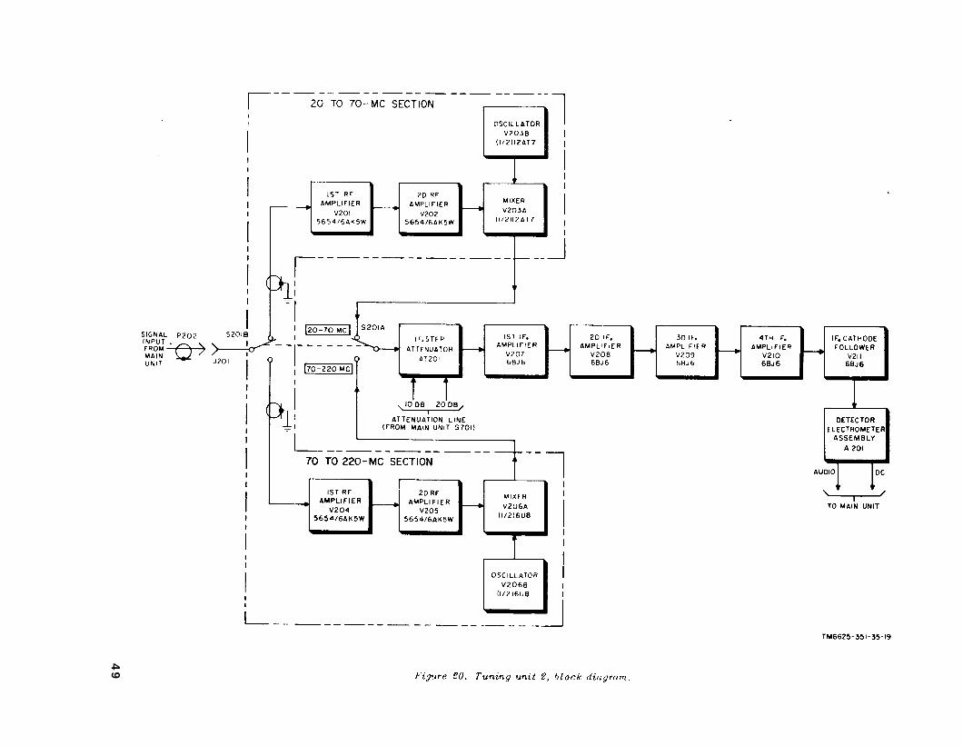
Figure 20.
49
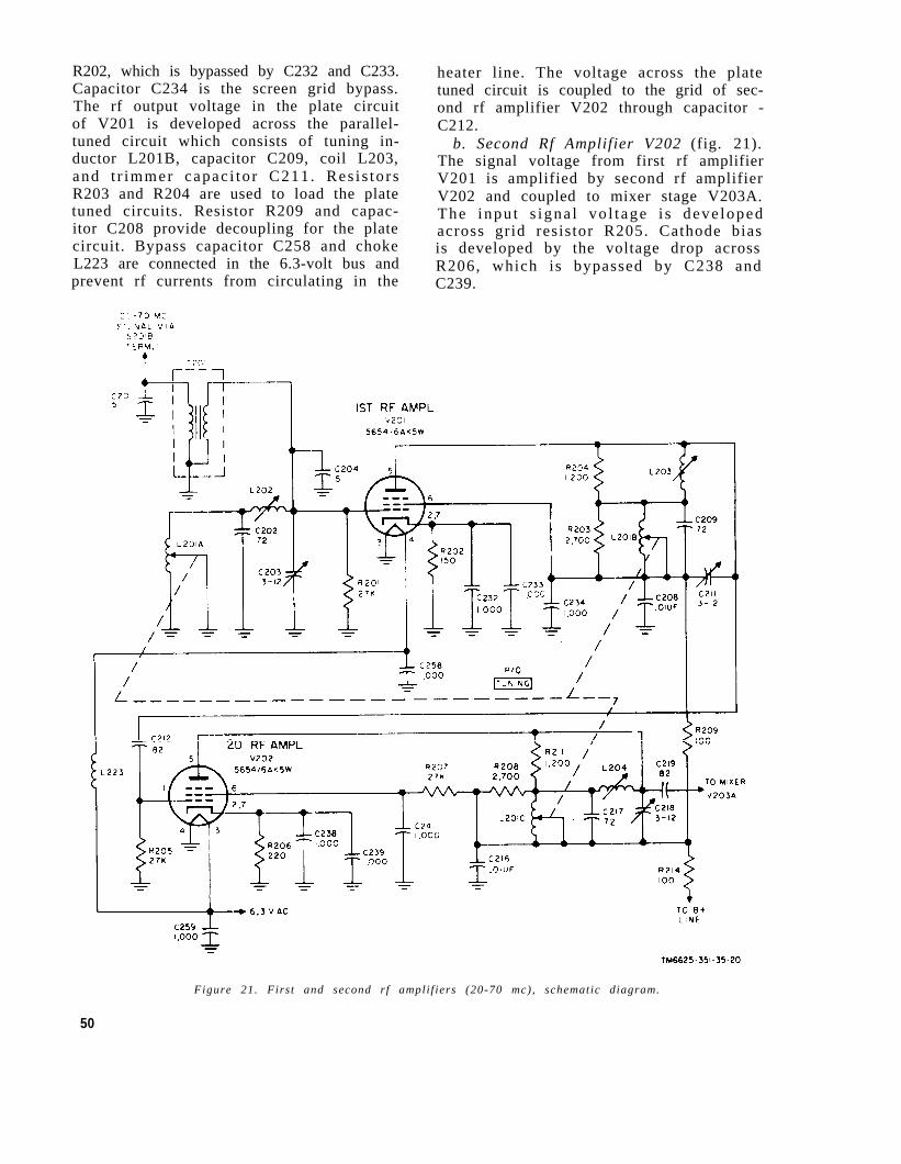
R202, which is bypassed by C232 and C233.Capacitor C234 is the screen grid bypass.The rf output voltage in the plate circuitof V201 is developed across the parallel-tuned circuit which consists of tuning in-ductor L201B, capacitor C209, coil L203,and t r immer capac i to r C211 . Res i s to r sR203 and R204 are used to load the platetuned circuits. Resistor R209 and capac-itor C208 provide decoupling for the platecircuit. Bypass capacitor C258 and chokeL223 are connected in the 6.3-volt bus andprevent rf currents from circulating in the
heater line. The voltage across the platetuned circuit is coupled to the grid of sec-ond rf amplifier V202 through capacitor -C212.
b. Second Rf Amplifier V202 (fig. 21).The signal voltage from first rf amplifierV201 is amplified by second rf amplifierV202 and coupled to mixer stage V203A.The inpu t s igna l vo l t age i s deve lopedacross grid resistor R205. Cathode biasis developed by the voltage drop acrossR206, which is bypassed by C238 andC239.
Figure 21. First and second rf ampli f iers (20-70 mc), schematic diagram.
50
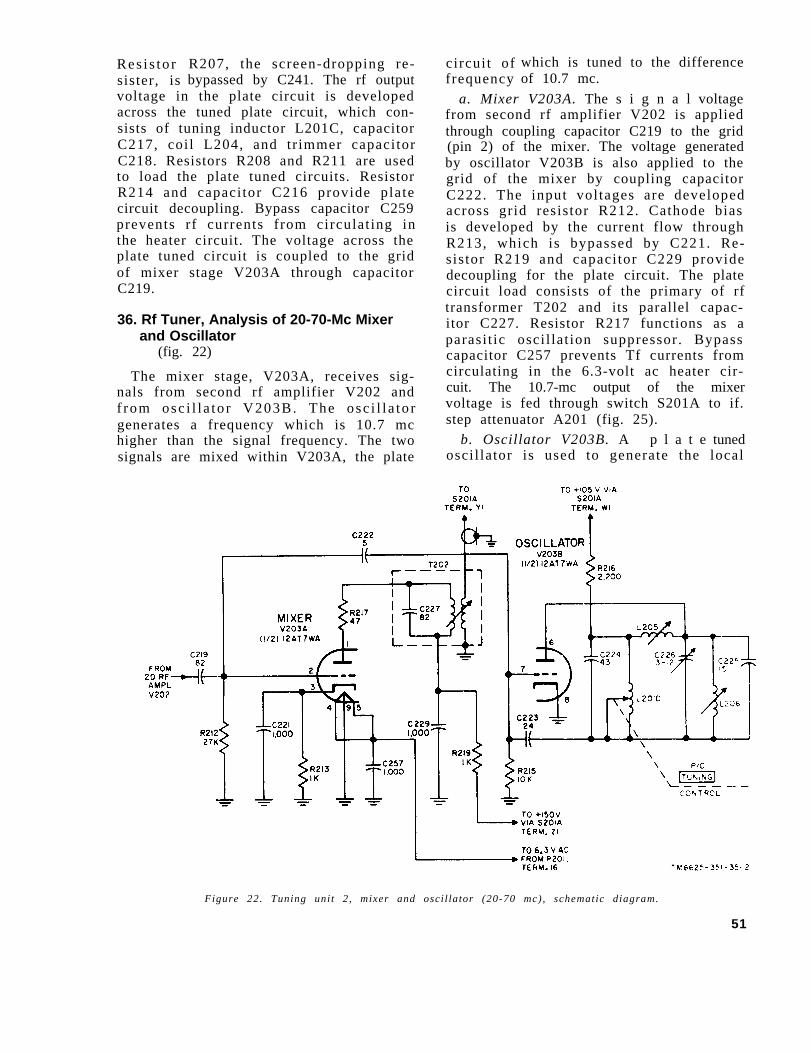
circuit offrequency
Res i s to rsister, is
R207, the screen-dropping re-bypassed by C241. The rf output
voltage in the plate circuit is developedacross the tuned plate circuit, which con-sists of tuning inductor L201C, capacitorC217, coil L204, and tr immer capacitorC218. Resistors R208 and R211 are usedto load the plate tuned circuits. ResistorR214 and capaci tor C216 provide platecircuit decoupling. Bypass capacitor C259prevents rf currents from circulat ing inthe heater circuit. The voltage across theplate tuned circuit is coupled to the gridof mixer stage V203A through capacitorC219.
36. Rf Tuner, Analysis of 20-70-Mc Mixerand Oscillator
(fig. 22)
The mixer stage, V203A, receives sig-nals from second rf amplifier V202 andf rom osc i l l a to r V203B. The osc i l l a to rgenerates a frequency which is 10.7 mchigher than the signal frequency. The twosignals are mixed within V203A, the plate
which is tuned to the differenceof 10.7 mc.
a. Mixer V203A. The s i g n a l voltagefrom second rf amplifier V202 is appliedthrough coupling capacitor C219 to the grid(pin 2) of the mixer. The voltage generatedby oscillator V203B is also applied to thegrid of the mixer by coupling capacitorC222. The input voltages are developedacross grid resistor R212. Cathode biasis developed by the current flow throughR213, which is bypassed by C221. Re-sis tor R219 and capaci tor C229 providedecoupling for the plate circuit. The platecircuit load consists of the primary of rftransformer T202 and its parallel capac-itor C227. Resistor R217 functions as aparasi t ic oscil lat ion suppressor. Bypasscapacitor C257 prevents Tf currents fromcirculating in the 6.3-volt ac heater cir-cuit. The 10.7-mc output of the mixervoltage is fed through switch S201A to if.step attenuator A201 (fig. 25).
b. Oscillator V203B. A p l a t e tunedoscil lator is used to generate the local
Figure 22. Tuning unit 2, mixer and osci l lator (20-70 mc), schematic diagram.
51
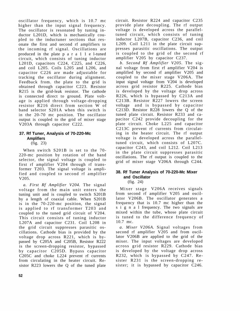
oscil lator frequency, which is 10.7 mchigher than the input s ignal frequency.The oscillator is resonated by tuning in-ductor L201D, which is mechanically cou-pled to the inductuner sections that res-onate the first and second rf amplifiers tothe incoming rf s ignal . Oscil lat ions areproduced in the plate p a r a 1 1 e l-tunedcircuit, which consists of tuning inductorL201D, capacitors C224, C225, and C226,and coil L205. Coils L205 and L206, andcapacitor C226 are made adjustable fortracking the oscillator during alignment.Feedback from. the plate to the grid isobtained through capacitor C223. ResistorR215 is the grid-leak resistor. The cathodeis connected direct to ground. Plate volt-age is applied through voltage-droppingresistor R216 direct from section W ofband selector S201A when this switch isin the 20-70 mc position. The oscillatoroutput is coupled to the grid of mixer stageV203A through capacitor C222.
37. Rf Tuner, Analysis of 70-220-McAmplifiers
(fig. 23)
When switch S201B is set to the 70-220-mc position by rotation of the bandselector, the signal voltage is coupled tofirst rf amplifier V204 through rf trans-former T203. The signal voltage is ampli-f ied and coupled to second rf amplif ierV205.
a. First Rf Amplifier V204. The signalvo l t age f rom the ma in un i t en te r s thetuning unit and is coupled to switch S201Bby a length of coaxial cable. When S201Bis in the 70-220-mc position, the signali s app l i ed to r f t r ans fo rmer T203 andcoupled to the tuned grid circuit of V204.This circui t consis ts of tuning inductorL207A and capacitor C231. Coil L208 inthe grid circuit suppresses parasitic os-cillations. Cathode bias is provided by thevoltage drop across R221, which is by-passed by C205A and C205B, Resistor R222is the screen-dropping resistor, bypassedby capac i to r C205D. Bypass capacitorC205C and choke L224 prevent rf currentsfrom circulating in the heater circuit. Re-sistor R223 lowers the Q of the tuned plate
52
circuit. Resistor R224 and capacitor C235provide plate decoupling. The rf outputvoltage is developed across the parallel-tuned circui t , which consists of tuninginductor L207B, capacitor C236, and coilL209. Coil L211 in the plate circuit sup-presses parasitic oscillations. The outputis coupled to the grid of the second rfamplifier V205 by capacitor C237.
b. Second Rf Amplifier V205. The sig-nal voltage from first rf amplifier V204 isamplified by second rf amplifier V205 andcoupled to the mixer stage V206A. Theinput signal voltage from V204 is developedacross grid resistor R225. Cathode biasis developed by the voltage drop acrossR226, which is bypassed by C213A andC213B. Resistor R227 lowers the screenvoltage and i s bypassed by capac i to rC213D. Resistor R228 lowers the Q of thetuned plate circuit. Resistor R233 and ca-pacitor C242 provide decoupling for theplate circuit. Choke L225 and capacitorC213C prevent rf currents from circulat-ing in the heater circuit. The rf outputvoltage is developed across the parallel-tuned circuit, which consists of L207C.capacitor C243, and coil L212. Coil L213in the plate circui t suppresses parasi t icoscillations. The rf output is coupled to thegrid of mixer stage V206A through C244.
38. Rf Tuner Analysis of 70-220-Mc Mixerand Oscillator
(fig. 24)
Mixer s t age V206A receives signalsfrom second rf amplifier V205 and oscil-lator V206B. The oscillator generates afrequency that is 10.7 mc higher than thes i g n a l frequency. The two signals aremixed within the tube, whose plate circuitis tuned to the difference frequency of10.7 mc.
a. Mixer V206A. Signal voltages fromsecond rf amplifier V205 and from oscil-lator V206B are applied to the grid of themixer. The input voltages are developedacross g r idis developedR232, whichsister R231sister; i t is
resistor R229. Cathode biasby the voltage drop acrossis bypassed by C247. Re-is the screen-dropping re-bypassed by capacitor C246.
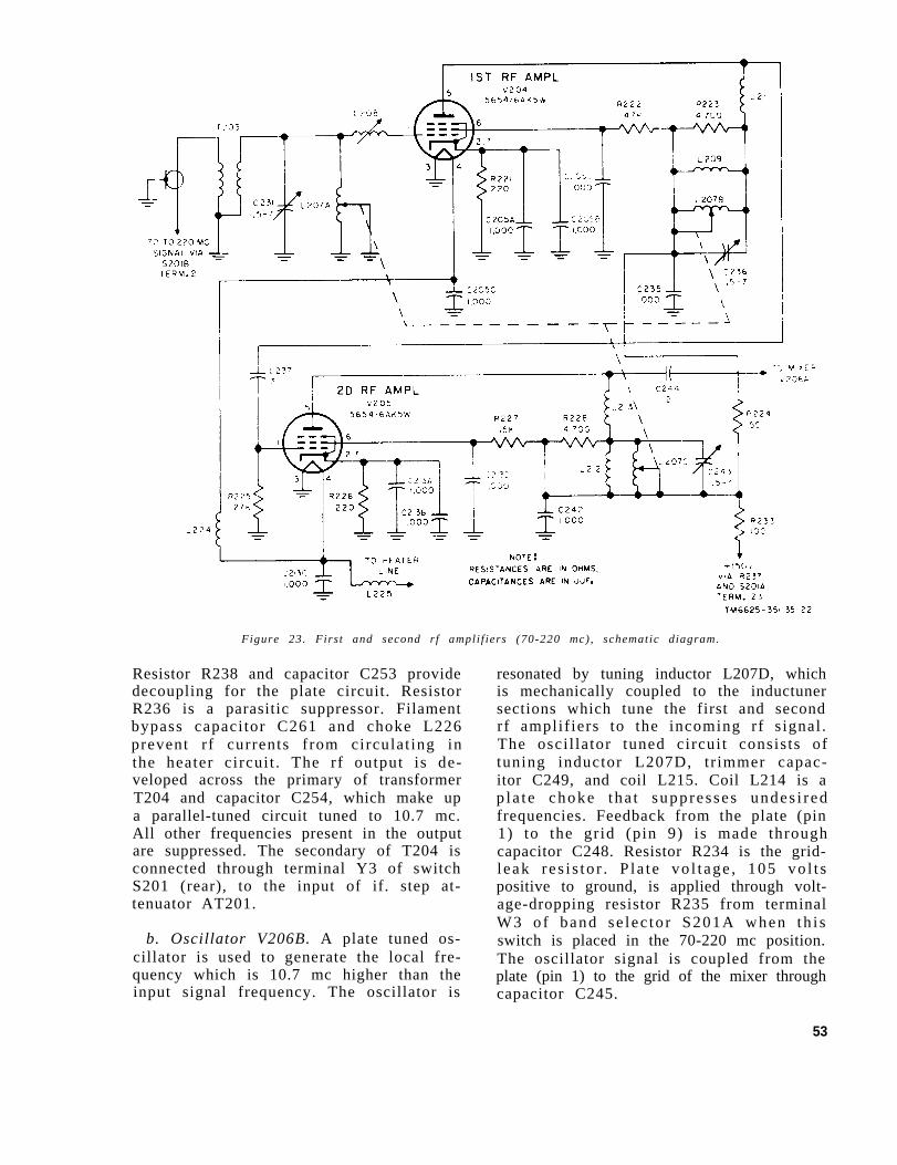
Figure 23. First and second rf ampli f iers (70-220 mc), schematic diagram.
Resistor R238 and capacitor C253 providedecoupling for the plate circuit. ResistorR236 is a parasitic suppressor. Filamentbypass capacitor C261 and choke L226prevent rf currents from circulat ing inthe heater circuit . The rf output is de-veloped across the primary of transformerT204 and capacitor C254, which make upa parallel-tuned circuit tuned to 10.7 mc.All other frequencies present in the outputare suppressed. The secondary of T204 isconnected through terminal Y3 of switchS201 (rear), to the input of if. step at-tenuator AT201.
b. Oscillator V206B. A plate tuned os-cillator is used to generate the local fre-quency which is 10.7 mc higher than theinput signal frequency. The oscillator is
resonated by tuning inductor L207D, whichis mechanically coupled to the inductunersections which tune the first and secondrf amplif iers to the incoming rf s ignal .The osci l lator tuned circui t consists oftuning inductor L207D, tr immer capac-itor C249, and coil L215. Coil L214 is ap la t e choke tha t suppresses undes i r edfrequencies. Feedback from the plate (pin1) to the grid (pin 9) is made throughcapacitor C248. Resistor R234 is the grid-l eak re s i s to r . P la t e vo l t age , 105 vo l t spositive to ground, is applied through volt-age-dropping resistor R235 from terminalW3 of band se lec to r S201A when th i sswitch is placed in the 70-220 mc position.The oscillator signal is coupled from theplate (pin 1) to the grid of the mixer throughcapacitor C245.
53
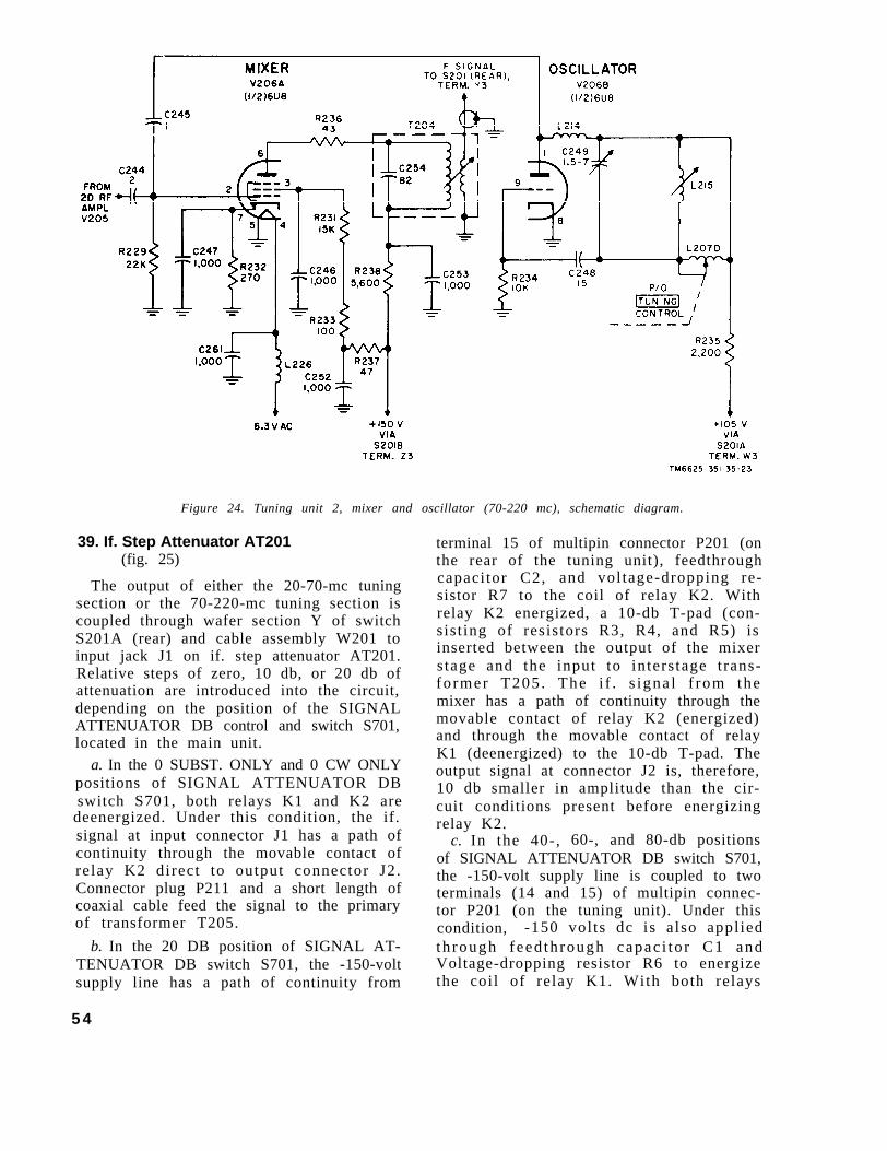
Figure 24. Tuning unit 2, mixer and oscillator (70-220 mc), schematic diagram.
39. If. Step Attenuator AT201(fig. 25)
The output of either the 20-70-mc tuningsection or the 70-220-mc tuning section iscoupled through wafer section Y of switchS201A (rear) and cable assembly W201 toinput jack J1 on if. step attenuator AT201.Relative steps of zero, 10 db, or 20 db ofattenuation are introduced into the circuit,depending on the position of the SIGNALATTENUATOR DB control and switch S701,located in the main unit.
a. In the 0 SUBST. ONLY and 0 CW ONLYpositions of SIGNAL ATTENUATOR DBswitch S701, both relays K1 and K2 are
deenergized. Under this condition, the if.signal at input connector J1 has a path ofcontinuity through the movable contact ofrelay K2 direct to output connector J2.Connector plug P211 and a short length ofcoaxial cable feed the signal to the primaryof transformer T205.
b. In the 20 DB position of SIGNAL AT-TENUATOR DB switch S701, the -150-voltsupply line has a path of continuity from
5 4
terminal 15 of multipin connector P201 (onthe rear of the tuning unit), feedthroughcapacitor C2, and voltage-dropping re-sistor R7 to the coil of relay K2. Withrelay K2 energized, a 10-db T-pad (con-sist ing of resistors R3, R4, and R5) isinserted between the output of the mixerstage and the input to interstage trans-fo rmer T205 . The i f . s igna l f rom themixer has a path of continuity through themovable contact of relay K2 (energized)and through the movable contact of relayK1 (deenergized) to the 10-db T-pad. Theoutput signal at connector J2 is, therefore,10 db smaller in amplitude than the cir-cuit conditions present before energizingrelay K2.
c. In the 40-, 60-, and 80-db positionsof SIGNAL ATTENUATOR DB switch S701,the -150-volt supply line is coupled to twoterminals (14 and 15) of multipin connec-tor P201 (on the tuning unit). Under thiscondition, -150 vol ts dc is a lso appliedth rough feed th rough capac i to r C1 andVoltage-dropping resistor R6 to energizethe coil of relay K1. With both relays
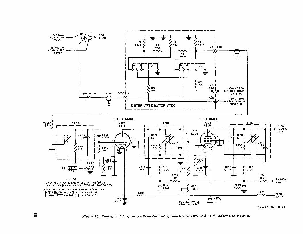
Figure 25.
55
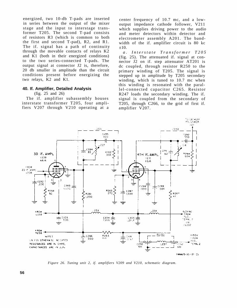
energized, two 10-db T-pads are insertedin series between the output of the mixerstage and the input to interstage trans-former T205. The second T-pad consistsof resistors R3 (which is common to boththe first and second T-pad), R2, and R1.The if . s ignal has a path of continuitythrough the movable contacts of relays K2and K1 (both in their energized conditions)to the two series-connected T-pads. Theoutput signal at connector J2 is, therefore,20 db smaller in amplitude than the circuitconditions present before energizing thetwo relays, K2 and K1.
40. If. Amplifier, Detailed Analysis(fig. 25 and 26)
The if . amplifier subassembly housesinterstate transformer T205, four ampli-fiers V207 through V210 operating at a
center frequency of 10.7 mc, and a low-output impedance cathode follower, V211which supplies driving power to the audioand meter detectors within detector andelectrometer assembly A201. The band-width of the if. amplifier circuit is 80 kc±10.
a . I n t e r s t a t e T r a n s f o r m e r T 2 0 5(fig. 25). The attenuated if. signal at con-nector J2 on if. step attenuator AT201 isdc coupled, through resistor R250 to theprimary winding of T205. The signal isstepped up in amplitude by T205 secondarywinding, which is tuned to 10.7 mc whenthis winding is resonated with the paral-l e l - connec ted capac i to r C265 . Res i s to rR247 loads the secondary winding. The if.signal is coupled from the secondary ofT205, through C266, to the grid of first if.amplifier V207.
Figure 26. Tuning unit 2, if. amplifiers V209 and V210, schematic diagram.
56
b. If. Amplifiers K207 and V208 (fig. 25).Although al l four if . amplif iers are es-sentially the same in function and descrip-tion, the method of biasing V207 and V208differs from that employed in the circuitsfor V209 and V210 (fig. 26). A second dif-ference exists because double-tuned trans-formers are connected in the plate circuitsof V207 and V208; single-tuned impedancenetworks are suff icient to maintain thedes i r ed se l ec t iv i ty in th i rd and four thamplifiers, V209 and V210 (fig. 26).
(1)
(2)
The secondary o f i f . i n t e r s t agetransformer T205 is tuned to 10.7rnc and feeds the signal to the con-trol grid of V207 through capacitorC266. Cathode bias is supplies bythe voltage drop across R249, whichis bypassed by C268. Grid resistorR248 is connected through feed-through capacitor C267 to the var-iable arm of GAIN control R241.The feedthrough capacitor func-tions as an rf bypass and couplesthe bias voltage from the panel-mounted GAIN control to the grid ofV207. The amplification of the sig-nal through V207 is dependent onthe bias voltage applied to the grid(pin 1) through GAIN control R241.Resistor R251, bypassed by C273,d e c r e a s e s t h e s c r e e n g r i d a n dplate voltage. Resistor R254 andcapacitor C269 provide decouplingfor the plate and screen circuits.Bypass capacitors C299 and C302,toge the r wi th chokes L231 andL232 , p reven t r f cu r ren t s f romcirculat ing in the heater circuit ,The output of V207 is applied to thep r i m a r y o f T 2 0 6 . T h e p r i m a r ywinding and the parallel capacitor,C272 , r e sona te toge the r a t t heintermediate frequency. The out-put of T206, developed across thesecondary wind ing and pa ra l l e lcapacitor C274, is coupled to sec-ond if . amplif ier V208. ResistorR253 lowers the Q of the trans-former tuned circuit.The signal from tuned transformerT206 is coupled through capacitorC275 to the grid of second if. am-
plifier V208. Capacitor C275 pre-vents the bias voltage from short-ing to ground. Grid resistor R252is connected to a fixed source ofnegative bias potential (R244 andR245) through feedthrough capac-itor C271. Resistors R244 and R245form a vo l t age -d iv ide r ne tworkfor the -15-volt bias line and arephyscially 10 c a t e d on terminalboard TB201 (fig. 64). Except fort h e d i f f e r e n c e i n b i a s i n g , c o r -responding parts in the second if.amplifier state function identicallywith those in the first if. amplifierstage.
c. If. Amplifiers V209 and V210 (fig. 26).The output of second if. amplifier V208 iscoupled to the grid of third if. amplifierV209. This s tage operates with cathodebias developed across resistor R259, whichis bypassed by capacitor C282. ResistorR261, bypassed by C283, decreases thescreen grid and plate voltage. Tuned coilL227 completes the dc path to the plate(pin 5) of amplifier V209. Resistor R263and capaci tor C286 provide decoupling.Addit ional decoupling in the +150-voltsupply line is provided by low-pass filterFL201. This f i l ter permits the 150-voltB+ output from the power supply to becoupled through feedthrough capacitorsC297 and C296 to the 150-volt bus in theif. amplifier subassembly; simultaneously,the filter coil presents a high-impedanceinput to the 10.7-mc frequencies presentin the plate and screen circuits. Bypasscapacitors C303, C304, and C305, togetherwith chokes L233 and L234, prevent rfcurrents from circulat ing in the heatercircuit. A second low-pass filter network,FL202, provides additional protection inassuring that the heater power source isfree of residual rf and if. currents. Theoutput of V209 is applied to tuned imped-ance network Z201. This network consistsof tuned coil L227, which resonates withcapacitor C284 to the desired center fre-quency of 10.7 mc. Capacitor C285 is in-cluded within the shielded network, andcouples the output to fourth if. amplifierV210. Resistor R262, also housed withinthe shield, is the grid return for V210.
57
The fourth if. amplifierin an iden t i ca l manner
(V210) operateswith V209. The
output signal from the tuned impedancenetwork 2202 is coupled to i f . cathodefollower V211.
d. If. Cathode Follower V211 (fig. 32).A cathode follower is used as the f inalstage in the if . amplif ier subassembly.This stage is identical in circuit compo-nents with the if. cathode follower in tuningunits 2, 3, and 4. Therefore, the followingcircuit description is applicable to all if.cathode followers, with differences indi-cated in the chart that follows the circuitanalysis .
(1)
(2)
The function of the if. cathode fol-lower is to supply driving power tothe detectors in the detector andelectrometer circuit from a low-impedance source.
A pentode-type 6BJ6 tube is usedas the if. cathode follower; sincethe sc reen g r id , t he suppresso rgrid, and the plate are externallyconnected together, the tube func-tions like a triode. The if. signalfrom the final if. amplifier is cou-pled to the grid of the triode. Theresistor housed within the imped-ance network of the final if. ampli-fier functions as the grid return.
(3)
(4)
(5)
(6)
Cathode bias is employed; the biasresistor is bypassed by a capac-itor. A tuned coil is in series withthe cathode bias network to chassisground. This coil is adjusted dur-ing if. amplifier alignment to de-velop maximum signal output.
The c o m m o n junction of thescreen grid, the suppressor grid,and the plate is bypassed to groundthrough a capacitor . Plate volt-age is applied from the f i l tered150-volt bus through a droppingr e s i s t o r .
The hea te r c i r cu i t i s decoup ledf r o m t h e 6 . 3 - v o l t a c p o w e rsource by a f i l ter capacitor andrf choke.The rf voltage developed acrossthe cathode tuned coil is appliedto a connector plug on the rearpartition of the if. amplifier sub-a s s e m b l y. This connector plugmates direct with input jack J1 onthe detector and electrometer as-sembly.
The following chart summarizesthe d i f fe rences be tween the i f .cathode followers in tuning units2, 3, and 4.
C o m p o n e n t Tun ing un i t Tun ing un i t Tun ing un i t2 3 4
If. cathode followerGrid input parasitic suppressorCathode bias resistorCathode bypass capacitorPlate voltage-dropping resistor and bypass capacitorPlate decoupling networkHeater decoupling circuitTuned cathode inductanceOutput connector
V211NoneR271C293R272 and C294R269 and C295C306 and L235L229P212
V410R462R463C488R464 and C491R459 and C492C489 and L432L431P413
V512R584R585C593R586 and C594R581 and C603C609 and L542L535P514
41. Detector and Electrometer sepa ra te aud io and dc me te r ing s igna lAssembly A201 channels, and applies output signals to the
(fig. 19) appropr i a t e c i r cu i t s i n the ma in un i t .These sealed assemblies are interchange-
All tuning units use an identical sealed able with each other and perform the func-detector and electrometer assembly. Each tions described in detail for detector andassembly receives driving power from the electrometer assembly A1 within tuningif . amplif ier , separates the s ignal into unit 1 (para 32 and 33).
58
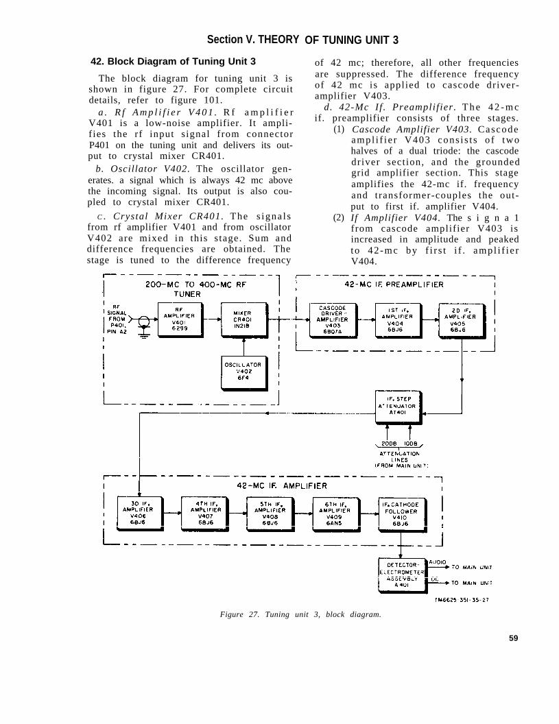
Section V. THEORY
42. Block Diagram of Tuning Unit 3
The block diagram for tuning unit 3 isshown in figure 27. For complete circuitdetails, refer to figure 101.
a . R f A m p l i f i e r V 4 0 1 . R f a m p l i f i e rV401 is a low-noise amplifier. It ampli-f ies the rf input s ignal from connectorP401 on the tuning unit and delivers its out-put to crystal mixer CR401.
b. Oscillator V402. The oscillator gen-erates. a signal which is always 42 mc abovethe incoming signal. Its output is also cou-pled to crystal mixer CR401.
C . Crystal Mixer CR401. The s igna l sfrom rf amplifier V401 and from oscillatorV402 are mixed in this s tage. Sum anddifference frequencies are obtained. Thestage is tuned to the difference frequency
OF TUNING UNIT 3
of 42 mc; therefore, all other frequenciesare suppressed. The difference frequencyof 42 mc is applied to cascode driver-amplifier V403.
d. 42-Mc If . Preamplif ier. T h e 4 2 - m cif. preamplifier consists of three stages.
(1)
(2)
Cascode Amplifier V403. Cascodeampl i f i e r V403 cons i s t s o f twohalves of a dual triode: the cascodedriver sect ion, and the groundedgrid amplifier section. This stageamplifies the 42-mc if. frequencyand transformer-couples the out-put to first if. amplifier V404.If Amplifier V404. The s i g n a 1from cascode amplifier V403 isincreased in amplitude and peakedto 42-mc by f i r s t i f . ampl i f i e rV404.
Figure 27. Tuning unit 3, block diagram.
59
(3) If. Amplifier V405. Further signalgain and selectivity are increasedby coupling the output of V404 to if.amplifier V405. Its output is trans-former-coupled to the input of if.step attenuator AT401.
e. If. Step Attenuator AT401. T h e if.a t t enua to r i s a l adder ne twork wi th aminimum insertion loss of 6-db and twoadditional steps of 10-db and 20-db. Sincethe 6-db loss is always in the system, theeffect that is that of a three-position at-tenuator with steps of 0, 10, and 20-db. Theamount of attenuation introduced is con-trolled by the position of wafer switch S701,located in the main unit. The output from if.step attenuator AT401 is fed to the input ofthe 42-mc if. amplifier.
f . I f . Ampli f iers V405 through V409.If. amplifier V406 receives the output of theif. step attenuator and couples the attenu-ated signal to the following three stages forfurther gain and selectivity. Each stage istuned to 42-mc.
g. Cathode Follower V410. Cathode fol-lower V410 is used to obtain a low-im-pedance source to feed detector and elec-trometer assembly A401.
h. Detector and Electrometer Assem-bly. This assembly is identical in functionand parts to the interchangeable detectorand electrometer used in tuning units 1and 2 (para 25j and 41). The electrometerstages present a high impedance to thesignal from the meter detector. Therefore,no signal loss is made in coupling the de-tected peak or average envelope voltage tocathode follower V702 in the main unit.
43. RF Amplifier V401, Detailed Analysis(fig. 28, 68, and 69)
The signal voltage from the main unitis coupled to rf amplifier V401. A type6299 grounded grid t r iode amplif ier ofplanar electrode construction is used be-cause of its low-noise characteristic. Theright side of the rf tuner is separated fromthe left side by a grounded center parti-tion (fig. 69). The amplifier tube is housedwithin the rf tuner (right side) which isdivided into two sections (B, fig. 69) bya grounded partition. This partition sep-
arates the tuned cathode input circuit fromthe tuned plate output circuit. The tunedplate and cathode circui ts add gain andselectivity to the rf amplifier. The entirerf tuner, which houses the rf amplifier,the local oscillator, and the crystal mixer,is shockmounted within the tuning unit. Therubber pads of the shockmounts absorb vi-b ra t iona l e f fec t s and p reven t spur iousinterference that might be introduced bymicrophonics of the local osillator.
a. Input Signal Path. The parts locationdiagram for tuning unit 3 (fig. 68) showsthat the signal voltage from terminal A2on mult ipin connector P401 is coupledthrough connector plug P402 and r ight-angle adapter CP401 to the input of rff i l t e r FL401 . Th i s se lec t ive f requencyfilter has a bandpass characteristic whichcorresponds to the 200-400-mc frequencyrange of the tuning unit. Other uhf fre-quencies, such as television channels andmil i tary communicat ion channels in theadjacent spectral region are effect ivelyblocked from entering the rf amplif ierinput circuit. The output of filter FL401i s app l i ed th rough r igh t -ang le adap te rCP402 to coaxial cable assembly W401.Connector plug P406, which terminatescable assembly W401, couples the signalto mating jack J405 at the input to the rftuner subassembly (B, fig. 69). The signalis fed to a tuned circuit which consists ofthe closely coupled rf input coils, L401and L402.
b. Ampli f ier Circuit (fig. 28 and 69).The tuned cathode input circuit consists ofpickup loop L402, trimmer capacitor C401,and va r i ab le capac i to r C402 which i sworm-gear driven by the front panel TUN-ING control. Variable capacitor C402 ismechanically coupled to plate-tuning ca-pacitor C404 and to oscillator-tuning ca-pac i to r C413 . There fore , the ampl i f i e rand the oscillator track over the completefrequency range. The low rf potential sideof the cathode inlut tuned circuit is by-passed by C403. The amplified rf voltagein the plate is developed across the paral-lel-tuned circuit, which consists of tuningcapaci tor C404 and pickup loop L404.Trimmer capacitor C405 is adjusted dur-ing alignment to obtain a peak output signal
60
from the amplif ier plate circuit at the400-mc high-frequency end of the band.
(1) The dc path for applying B+ voltageto the plate of the amplifier is un-conventional because the plate ofthe coplanar triode is located on theleft side of the grounding partition(A, fig. 69) in the rf tuner. The dcpath consists of the following cir-cuit elements:
{a)
(b)
(c)
(d)
(e)
(4)
The voltage set by the arm ofV 4 0 1 A D J c o n t r o l R 4 0 5 ( a nalignment adjustment control) isfed to fixed resistor R402, whichis mounted on the rear of the rftuner (A, fig. 69). The low poten-tial terminal of R402 is connectedto the p ro t rud ing t e rmina l o ffeedthrough capacitor C410.This feedthrough capacitor by-p a s s e s r f c u r r e n t s t o t h egrounded r f t une r chass i s andc o n d u c t s the plate voltagethrough the chassis to the in-terior of the cathode input cir-cuit.A wire lead conducts the B+ po-tential to a second feedthroughcapac i to r , C409 (B , f ig . 69) ,which is mounted through thegrounded part i t ion which sepa-rates the cathode input circuitfrom the plate output circui t .Resistor R401 is connected fromthe plate side of C409 to bypasscapacitor C406. This network de-couples the rf amplif ier s tagefrom the B+ power supply.Rf choke L406 adds to the de-coupling network by offering ahigh impedance to frequencies inthe uhf spectrum, and applies theB+ po ten t i a l t o the cen te r o fpickup loop L404, which is partof the plate tuned circuit.A metallic bar to which LA04 ismounted completes the dc pathto the plate of the rf amplifiertube.
(2) The ac path for applying 6.3-volt ( 3 )heater voltage to the f i lament ofthe rf amplif ier is also unusualbecause the hea te r vo l t age l ead
mus t be b rough t i n to the r igh tside of the rf tuner through thecen te r pa r t i t ion . The ac hea te rpath consists of the following cir-cuit elements:
(a)
(b)
(c)
The 6.3-volt ac l ine continuesf rom the i f . p reampl i f i e r sub-assembly to rf choke L414, whichis mounted between an insulatedtie-point terminal on the rear ofthe rf tuner (A, fig. 69) and thei n n e r conducting terminal off e e d t h r o u g h c a p a c i t o r C 4 1 1 ,which bypasses r f cu r ren t s toground.The inner conducting terminal ofC411 penetrates the rear of therf tuner and applies the ac volt-age through rf choke L408 to asecond feed th rough capac i to r ,C407. This feedthrough elementpenetrates t h e upright centerp a r t i t i o n w h i c h s e r v e s a s aAmounting surface for the threetuning capacitors , C402, C404,and C413 (B , f ig . 69) . Feed-through capacitor C407 furtherfilters the 6.3-volt ac power sup-ply.The inner conducting terminal ofC407 connects the ac heater volt-age to an rf choke, L407, which isconnected in series with the elec-tron tube heater. A metallic clipconnects the 6.3-volt ac voltageto the cylindrical heater elec-trode which protrudes from oneend of the electron tube. ‘Theheater return circuit to chassisground is completed within thetube enve lope by the commonheater and the cathode ring. Thering is connected to the tunedcathode input LC circuit, whichconsists of pickup loop L402 andtun ing capac i to r C402 . Se r i e scoil LA403 completes the 6.3-voltac c i r cu i t t o r f tune r chass i sground.
The rf output of amplifier V401 isinductively coupled to crystal diodeCR401 th rough co i l s L404 andL405.
6 1
Figure 28. Tuning unit 3 rf amplifier and oscillator, schematic diagram.
44. Oscillator V402, Detailed Analysis(fig. 28 and 69)
A tuned plate oscillator which employs anacorn, type 6F4 (V402), generates an rffrequency which is 42-mc higher than theinput signal frequency. The oscillator istuned by capacitor C413, which is mechan-ically coupled to C402 and C404 in the
62
rf amplifier cathode input and plate outputcircuits. Oscillations are developed in theV402 tuned path circuit which consists ofcoil L409, f ixed capacitor C412, tuningcapac i to r C413 , and t r immer capac i to rC414. Feedback from the plate (pins 3and 4) to the grid (pin 5) is made throughcapacitor C415. Resistor R406 is the grid
resistor. Coil L411, which is wound on re-sistor R403, functions as a parasitic sup-pressor. Plate voltage is f i l tered by re-sis ters R404, R407, and R408, togetherwith bypass capacitor C416. Feedthroughcapacitors C421 and C422 are best de-scribed by reference to the physical viewof the rf tuner (fig. 69).
a. +105- Volt Dc Power Path. The dc pathfor applying +105-volts to the plate of os-ci l lator V402 consists of the fol lowingcircuit elements:
(1)
(2)
(3)
The +105-volt bus is connected tothe rear of the rf tuner (A, fig. 69)by a wire lead which connects tothe inner conductor of the feed-through bypass capaci tor , C422.An insu la t ed l ead connec t s the+105-volt bus from C422 to a sec-ond feedthrough capacitor, C421.This capacitor penetrates the up-right center partition which servesas a mounting surface for the threevariable tuning capacitors, C402,C404, and C413.Decoupling resistor R408 (B, fig.69) connects the dc voltage to thehigh-potential terminal of rf bypasscapac i to r C416 . The dc vo l t agecontinues through the series- con-nected decoupling resistors, R407and R404, and rf choke L411, to thel/4-inch wide loop of brass strap-ping mounted to the frame of C413.This strapping functions as a highQ inductor for the oscillator at theu l t r a -h igh f r equenc ies employedin tuning unit 3.
b. 6.3 Volt Ac Path. The ac pa th fo rapplying 6.3-volt ac voltage to the heaterof the osci l lator tube consists of feed-through capacitor C417, rf choke L413,and bypass capacitor C418. This decou-pling circuit is physically located withinthe rf tuner (B, fig. 69) as follows:
(1) A parallel path is provided insidethe rf tuner for heater voltage dis-tr ibut ion. One path is through rfchoke L408 for heater voltage (para43b(2)) to rf amplif ier V401. Asecond pa th i s p rov ided by theInsulated lead which connects the
(2)
heater voltage from feedthroughC 4 1 1 t o f e e d t h r o u g h c a p a c i t o rC417. Rf choke L413 and bypass ca-pacitor C418 prevent rf currentsfrom circulating in the heater sup-ply circuit.Feedthrough capacitor C417 pene-trates the upright center partitionon which tuning capacitors C402,C404, and C413 are mounted. Theinner conductor of the feedthroughcapacitor connects the heater volt-age to oscillator V402 heater (pin6). The second heater (pin 1) isconnected to the rf chassis groundto complete the heater circuit path.
c. Oscillator Power Signal Path. T h efrequency generated across oscillator coilL409 (B, f ig. 69) in V402 plate-to-gridcircuit is inductively coupled to the crystaldiode pickup coil L405. This coil is phys-ically located so that it is also within themagnetic field surrounding the rf ampli-fier plate circuit inductor loop, L404.
45. Crystal Mixer Circuit, DetailedAnalysis
(fig. 28)
The incoming rf signal and the oscillatoroutput signal are mixed in this stage. Thesignal from rf amplif ier plate inductorL404 is inductively coupled to mixer pickuploop L405. The signal from osci l lator-tuned c i r cu i t L409 , phys ica l ly loca tedabout 1 inch away from mixer pickup loopL405 (B, fig. 69), is also within the mag-netic field of L405 and inductively couplesthe oscillator signal to the crystal mixercircuit . The nonlinear characterist ics ofa crystal diode, CR401, are untilized forthe heterodyning process because of thefavorable s ignal- to-noise rat io obtainedat the high frequencies encountered in the200-400-mc f requency range o f tun ingunit 3. The diode produces a number offrequencies at its output circuit. Two ofthese a re the sum and d i f fe rence f re -quencies produced by the mixing process.Since pickup coil L405 and trimmer ca-pacitor C408 are resonated to 42-mc, thed i f fe rence f r equency i s passed th roughou tpu t co i l s L4-15-L416 and coup l ing
63
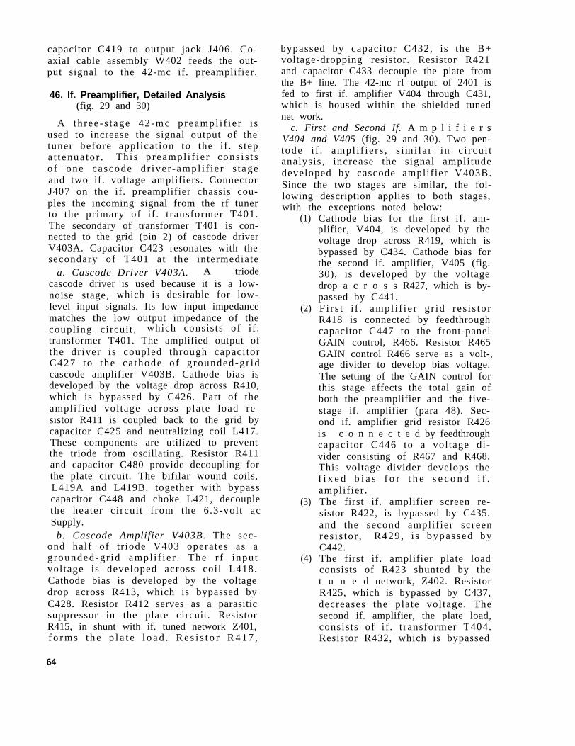
capacitor C419 to output jack J406. Co-axial cable assembly W402 feeds the out-put signal to the 42-mc if. preamplifier.
46. If. Preamplifier, Detailed Analysis(fig. 29 and 30)
A th ree - s tage 42-mc preampl i f i e r i sused to increase the signal output of thetuner before applicat ion to the if . s tepa t t enua to r . Th i s p reampl i f i e r cons i s t so f one cascode d r ive r -ampl i f i e r s t ageand two if. voltage amplifiers. ConnectorJ407 on the if. preamplifier chassis cou-ples the incoming signal from the rf tunerto the primary of if . t ransformer T401.The secondary of transformer T401 is con-nected to the grid (pin 2) of cascode driverV403A. Capacitor C423 resonates with thesecondary of T401 at the intermediate
a. Cascode Driver V403A. A triodecascode driver is used because it is a low-noise stage, which is desirable for low-level input signals. Its low input impedancematches the low output impedance of thecoupling circui t , which consists of i f .transformer T401. The amplified output ofthe driver is coupled through capaci torC427 to the ca thode o f g rounded-g r idcascode amplifier V403B. Cathode bias isdeveloped by the voltage drop across R410,which is bypassed by C426. Part of theamplif ied voltage across plate load re-sistor R411 is coupled back to the grid bycapacitor C425 and neutralizing coil L417.These components are utilized to preventthe triode from oscillating. Resistor R411and capacitor C480 provide decoupling forthe plate circuit. The bifilar wound coils,L419A and L419B, together with bypasscapacitor C448 and choke L421, decouplethe heater circuit from the 6.3-volt acSupply.
b. Cascode Amplifier V403B. The sec-ond half of t r iode V403 operates as ag rounded-gr id ampl i f i e r . The r f inpu tvoltage is developed across coi l L418.Cathode bias is developed by the voltagedrop across R413, which is bypassed byC428. Resistor R412 serves as a parasiticsuppressor in the plate circuit. ResistorR415, in shunt with if. tuned network Z401,f o r m s t h e p l a t e l o a d . R e s i s t o r R 4 1 7 ,
64
bypassed by capacitor C432, is the B+voltage-dropping resistor. Resistor R421and capacitor C433 decouple the plate fromthe B+ line. The 42-mc rf output of 2401 isfed to first if. amplifier V404 through C431,which is housed within the shielded tunednet work.
c. First and Second If. A m p l i f i e r sV404 and V405 (fig. 29 and 30). Two pen-tode i f . ampl i f i e r s , s imi la r in c i r cu i tanalysis , increase the signal ampli tudedeveloped by cascode amplif ier V403B.Since the two stages are similar, the fol-lowing description applies to both stages,with the exceptions noted below:
(1)
(2)
(3)
(4)
Cathode bias for the first if. am-plifier, V404, is developed by thevoltage drop across R419, which isbypassed by C434. Cathode bias forthe second if. amplifier, V405 (fig.30), is developed by the voltagedrop a c r o s s R427, which is by-passed by C441.F i r s t i f . ampl i f i e r g r id r e s i s to rR418 is connected by feedthroughcapacitor C447 to the front-panelGAIN control, R466. Resistor R465GAIN control R466 serve as a volt-,age divider to develop bias voltage.The setting of the GAIN control forthis stage affects the total gain ofboth the preamplifier and the five-stage if. amplifier (para 48). Sec-ond if. amplifier grid resistor R426i s c o n n e c t e d by feedthroughcapacitor C446 to a voltage di-vider consisting of R467 and R468.This voltage divider develops thef i x e d b i a s f o r t h e s e c o n d i f .amplif ier .The first if. amplifier screen re-sistor R422, is bypassed by C435.and the second amplif ier screenres i s to r , R429 , i s bypassed byC442.The first if. amplifier plate loadconsists of R423 shunted by thet u n e d network, Z402. ResistorR425, which is bypassed by C437,decreases the plate voltage. Thesecond if. amplifier, the plate load,consists of i f . t ransformer T404.Resistor R432, which is bypassed
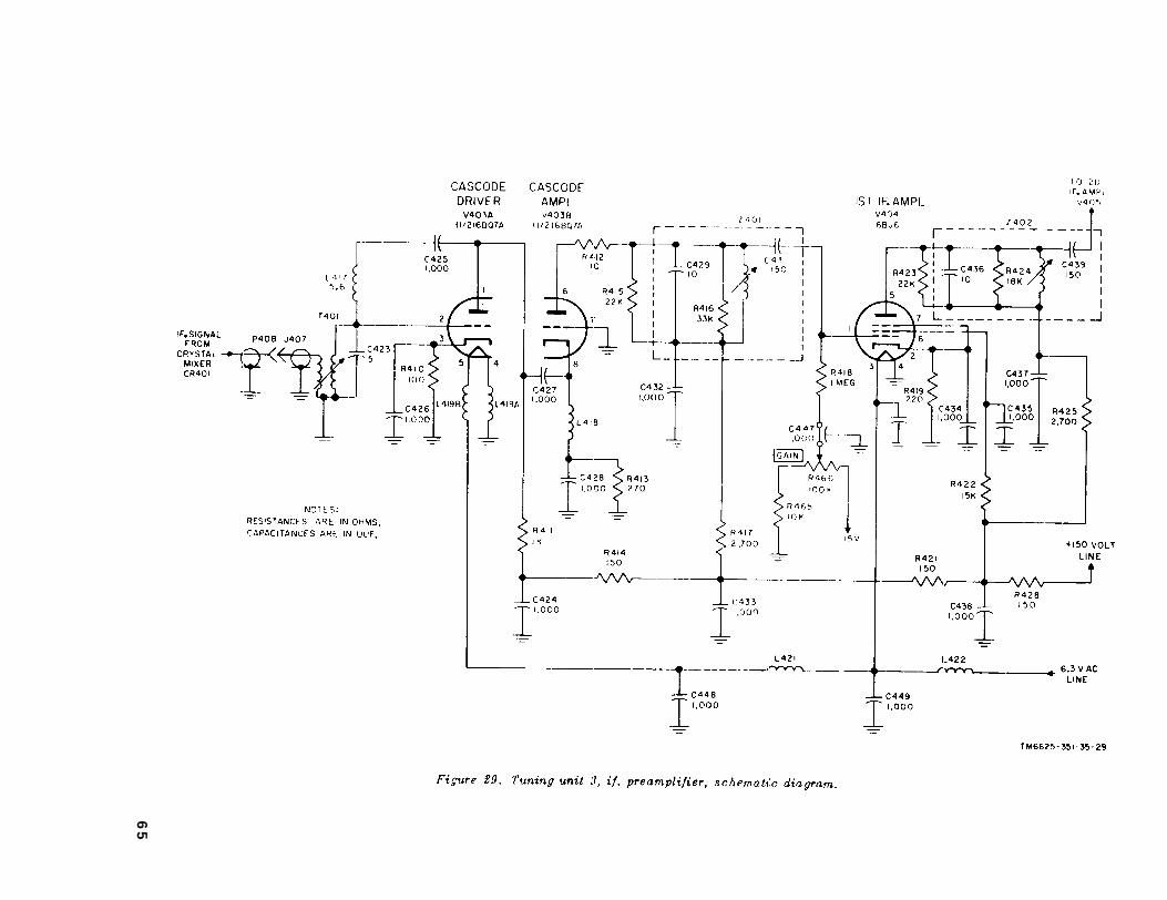
Figure 29.
65
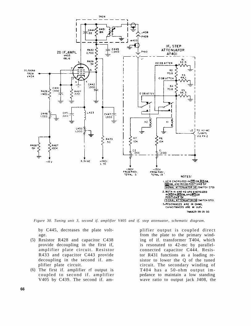
Figure 30. Tuning unit 3, second if. amplifier V405 and if. step attenuator, schematic diagram.
(5)
(6)
by C445, decreases the plate volt-age.Resistor R428 and capacitor C438provide decoupling in the first if,ampl i f i e r p la t e c i r cu i t . Res i s to rR433 and capacitor C443 providedecoupling in the second if. am-plifier plate circuit.The first if. amplifier rf output iscoup led to second i f . ampl i f i e rV405 by C439. The second if. am-
p l i f i e r ou tpu t i s coup led d i r ec tfrom the plate to the primary wind-ing of if. transformer T404, whichis resonated to 42-mc by parallel-connected capacitor C444. Resis-tor R431 functions as a loading re-sistor to lower the Q of the tunedcircuit. The secondary winding ofT404 has a 50 -ohm ou tpu t im-pedance to maintain a low standingwave ratio to output jack J408, the
66
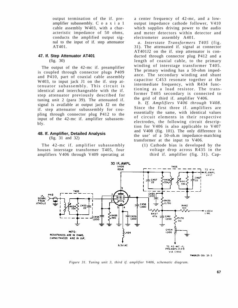
output termination of the if. pre-amplifier subassembly. C o a x i a 1cable assembly W403, with a char-acteristic impedance of 50 ohms,conducts the amplified output sig-nal to the input of if. step attenuatorAT401.
47. If. Step Attenuator AT401(fig. 30)
The output of the 42-mc if. preamplifieris coupled through connector plugs P409and P410, part of coaxial cable assemblyW403, to input jack J1 on the if. step at-t e n u a t o r s u b a s s e m b l y . T h i s c i r c u i t i sidentical and interchangeable with the if.s tep at tenuator previously described fortuning unit 2 (para 39). The attenuated if.signal is available at output jack J2 on theif. step attenuator subassembly for cou-pling through connector plug P412 to theinput of the 42-mc if. amplifier subassem-bly.
48. If. Amplifier, Detailed Analysis(fig. 31 and 32)
The 42-mc i f . ampl i f i e r subassemblyhouses interstage transformer T405, fouramplifiers V406 through V409 operating at
a center frequency of 42-mc, and a low-output impedance cathode follower, V410which supplies driving power to the audioand meter detectors within detector andelectrometer assembly A401.
a. Interstate Transformers T405 ( f i g .31). The attenuated if. signal at connectorAT401J2 on the if. step attenuator is con-ducted through connector plug P412 and alength of coaxial cable, to the primarywinding of interstage transformer T405.The primary winding has a 50-ohm imped-ance. The secondary winding and shuntcapacitor C453 resonate together at theintermediate frequency, with R434 func-t ion ing as a load re s i s to r . The t r ans -former T405 secondary is connected tothe grid of third if. amplifier V406.
b. I f . Ampli f iers V406 through V408.Since the f irst three if . amplif iers areessentially the same, with identical valuesof c i r cu i t e l emen t s in the i r r e spec t iveelectrodes, the following circuit descrip-tion for V406 is also applicable to V407and V408 (fig. 101). The only difference isthe use’ of a 50-oh.m impedance-matchingtransformer at the input to V406.
(1) Cathode bias is developed by thevoltage drop across R435 in thethird if. amplifier (fig. 31). Cap-
Figure 31. Tuning unit 3, third if. amplifier V406, schematic diagram.
67
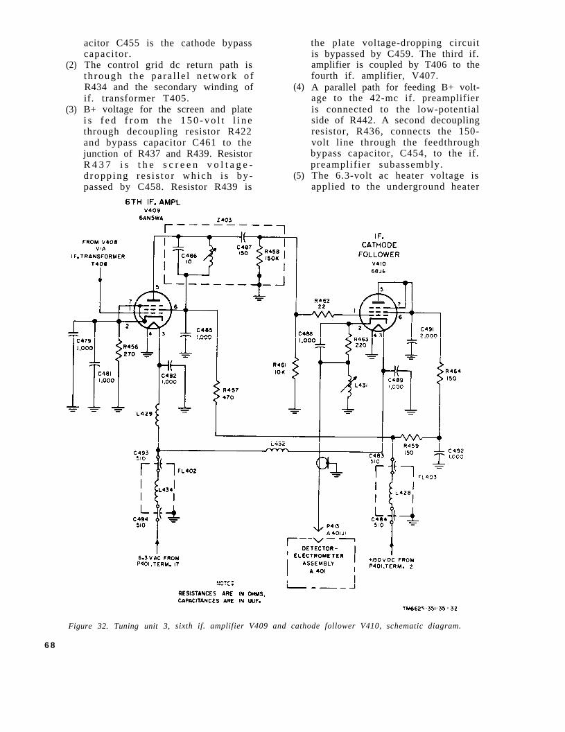
(2)
(3)
acitor C455 is the cathode bypasscapacitor .The control grid dc return path isth rough the pa ra l l e l ne twork o fR434 and the secondary winding of (4)if. transformer T405.B+ voltage for the screen and plate
passed by C458. Resistor R439 is
the plate voltage-dropping circuitis bypassed by C459. The third if.amplifier is coupled by T406 to thefourth if. amplifier, V407.A parallel path for feeding B+ volt-age to the 42-mc if. preamplifieris connected to the low-potentialside of R442. A second decouplingresistor, R436, connects the 150-volt line through the feedthroughbypass capacitor, C454, to the if.preamplif ier subassembly.The 6.3-volt ac heater voltage isapplied to the underground heater
i s f e d f r o m t h e 1 5 0 - v o l t l i n ethrough decoupling resistor R422and bypass capacitor C461 to thejunction of R437 and R439. ResistorR 4 3 7 i s t h e s c r e e n v o l t a g e -d ropp ing r e s i s to r wh ich i s by - (5)
Figure 32. Tuning unit 3, sixth if. amplifier V409 and cathode follower V410, schematic diagram.
6 8
(pin 4) through a decoupling net-work which consists of rf chokeL424 and bypass capacitor C456.
c. If. Amplifier V409 (fig. 32). The am-plified if. signal at the output of V408 isinductively coupled to the control grid ofif. amplifier V409. This stage is essen-tially similar to the first three if. ampli-f ier stages (b above), but differs in i tstuned plate circuit . The tuned network,Z403, in the output of the final if. ampli-f i e r , i s s ing le tuned . No se t -up t r ans -formations required because of the signalgain produced by the previous amplifiers t ages . Excep t fo r the lower va lue o fcathode bias resistor R456 and the plate-and screen-dropping resistor , R457, thecircuit description is identical with that ofif . amplif iers V406 through V408. Theheater circuit of V409 uses an additionaldecoupling network which isolates the 6.3-volt ac line from the if. and rf currentscirculating in the tuning unit. This addi-tional decoupling network consists of filterFL402, w h i c h c o n s i s t s o f a m e t a l l i ccylinder enclosing rf choke L434. Thec h o k e i s e n c a s e d w i t h i n t h e m e t a l l i ccylinder which penetrates the top side ofthe if, amplifier subassembly. The outersh ie ld o f the f i l t e r i s so lde red to thegrounded surface of the wall. Feedthroughcapacitor C494 accepts the 6.3-volt ac
voltage from the heater bus. Choke L434serves as a low-pass filter for powerlinefrequencies and a high rejection filter forintermediate frequencies. The 6.3-volt acis connected through feedthrough capacitorC493 to the junction of decoupling coilsL429 and L432.
d. If. Cathode Follower V410 (fig. 32).Detailed circuit analysis of the if. cathodefollower, which is identical in tuning units2, 3, and 4, appears in the description oftuning 2 (para 40d). The cathode followeris the final stage in the if. amplifier, whichs u p p l i e s d r i v i n g p o w e r f r o m a l o w -impedance source to the detectors in thedetector and electrometer assembly A401.
49. Detector and Electrometer Circuit A401(fig. 19)
All tuning units employ an identicals e a l e d d e t e c t o r a n d e l e c t r o m e t e r a s -sembly. E a c h c i r c u i t a c c e p t s d r i v i n gpower from the if. amplifier, detects thesignal in separate audio and dc meteringsignal channels , and applies output s ig-nals to the appropriate circuits in the mainunit . These sealed assemblies are inter-changeable with each other and perform thefunctions described in detail for detectorand electrometer circuit A1 within tuningunit 1 (para 32 and 33).
Section VI. THEORY OF TUNING UNIT 4
50. Block Diagram for Tuning Unit 4 plifier V501 receives the incoming
The block diagram for tuning unit 4 isshown in figure 33. For complete circuitdetails, refer to figure 102.
a. Rf Tuners. Two separa te r f tunersare employed in this tuning unit to housethe transmission-l ine types of rf ampli-fiers and oscillators. One tuner covers thefrequency spectrum from 700- to 1,000 -mc; ano the r covers the spec t rum f rom400- to 700-mc. The signal path througheach tuner is similar and is described asfollows :
(1) Tuner, 700-1,000. With FREQ-UENCY RANGE-MC switch S503set to 700-1,000-mc, first rf am-
rf signal which is coupled from themain unit to coaxial switch S501. Apath o f c o n t i n u i t y i s c r e a t e dthrough the coaxial switch to thedouble-tuned cavity in the inputside of V501. The amplified out-put of V501 present in i ts platecavity is coupled to a silicon diodecrystal mixer. Simultaneously, therf energy circulating in the oscil-lator cavity is coupled to the mixer.The oscil lator generates a signalthat tracks 42-mc higher than thei n c o m i n g r f s i g n a l . T h e m i x e rstage heterodynes the rf incomingsignal with the oscillator signal;
69
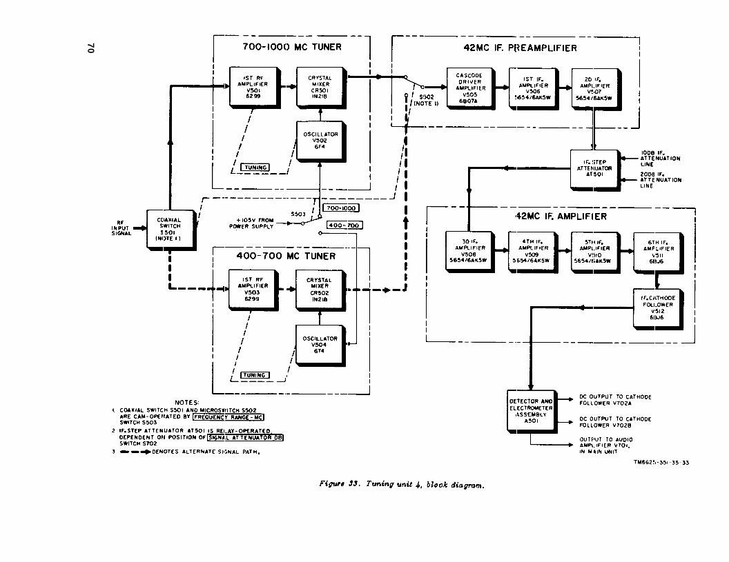
Figure 33.
70
(2)
(3)
th i s p roduces a d i f fe rence f re -q u e n c y o u t p u t t h a t i s c o u p l e dthrough microswitch S502 to the4 2 - m c i f . p r e a m p l i f i e r . T h emicroswitch, housed within the 42-mc i f . p reampl i f i e r , i s p lungeractuated by a cam on the shaft ofFREQUENCY RANGE-MC switchS503.
Tuner, 400-700 mc. The 400-700 -m c t u n e r f u n c t i o n s i d e n t i c a l l yw i t h t h e 7 0 0 - 1 , 0 0 0 - m c t u n e r ,except that FREQUENCY RANGE-MC switch S503 must be set to thelower frequency band for its oper-ation. Rf amplifier V503, crystalmixer CR502, and oscillator V504se rve the same purposes a s de -scribed in (1) above for the 700-1 ,000-mc tuner , wi th the osc i l -lator also tracking 42-mc abovethe incoming rf signal.
B+ switching. The B+ voltage forthe first rf amplifiers in either rftuner is not disconnected when thetuner becomes inopera t ive . Thedesign of the type 6299 planar elec-tron tube does not permit operationwith heater power applied and platevoltage disconnected. For this rea-son, both rf amplifiers V501 andV503 are energized, regardless oft h e p o s i t i o n o f F R E Q U E N C YRANGE-MC switch S503. However,B+ voltage is switched on to theoperat ive osci l lator and removedfrom the inoperative oscillator toassure that only one heterodynedsignal can pass to the if. amplifierchannel.
b. 42-MC If . Preamplif ier. T h e 4 2 - m cif . preamplifier consists of three stagesthat function identically with the if. pre-amplifier in tuning unit 3 (para 42d) in allrespects but one. The only difference be-tween the if. preamplifier in tuning units3 and 4 is the inclusion of a microswitchat the input to the tuning unit 4 if. pre-amplifier. This microswitch creates a pathof continuity from the energized rf tunerto the first stage of the preamplifier, whichis cascode driver-amplifler V505; simul-
taneously, the microswitch breaks the pathof continuity to V505 from the deenergizedrf tuner.
c. If. Step Attenuator AT501. If. s t e pattenuator AT501 is a ladder network witha minimum insertion loss of 6-db and twoadditional steps of 16-db and 26-db. Sincethe 6-db loss is always in the system, theeffect is that of a three-position attenuatorwith steps of 0, 10, and 20 db. The amountof attenuation introduced is controlled bythe position of SIGNAL ATTENUATOR DBswitch S701, located in the main unit .Output from if. step attenuator AT501 isfed to the input of the 42-mc if.amplif ier .
d. If. Amplifiers V508 through V511. If .amplifier V508 receives the output of theif. step attenuator and couples the atten-uated signal to three addit ional s tages.Each stage is tuned to a center frequencyof 42-mc.
e. If’. Cathode Follower V512. If. cath-ode follower V512 provides a low-imped-ance source to feed the amplified signalfrom the final if. amplifier stage to thedetector and electrometer assembly A501.
f. Detector and Electrometer Assembly.This assembly is identical in function andparts with the interchangeable detectorand electrometer assemblies used in tuningunit 1 (para 25j), tuning unit 2 (para 41),and tuning unit 3 (para 42h).
51. Rf Tuner, 700-1,000 Mc, Introduction(fig, 34)
The signal voltage from the main unitis fed to coaxial switch S501, which is con-trolled by the front-panel band selector.With the band selector rotated to the 700-1,000-mc posit ion, the signal voltage isconducted from the coaxial switch by cableassembly W502 and its connector plug P506to mating jack J506 on the exterior of therf tuner assembly.
a. Physical Description (fig. 34, 72, and74). A combined physical-electr ical dia-gram of the rf tuner (fig. 34) shows thatrf amplifier V501 and oscillator V502 arehoused in a chassis containing four tunedcoaxial-type cavities and two rectangularcompartments. The chassis is constructed
71
with relatively thick walls to provide a highdegree of mechanical stability and elec-trical isolation. Three covers (fig. 72) aresecured to the chassis; one cover is se-cured to the side of the chassis , and asecond cover is secured to the end of thetuner housing the variable capacitor plates.These two covers provide proper shield-ing against rf leakage for the amplif iercavit ies , the osci l lator cavity, and thecompartment that houses voltage-droppingresistor R505 in the oscillator plate cir-cuit . The third cover is secured to thecompar tmen t tha t houses c rys t a l d iodeCR501 and crystal mixer coil L505. Anaccess hole is provided at the top of thecover to permit factory adjustment of thetuning shaft for a flat frequency responseover the band. Reference to the parts loca-tion diagram (fig. 74) shows that four feed-through capacitors (C502, C505, C540, andC511), a right-angle input signal connector(J506), and a termination (CP501) are in-serted through the chassis walls for pur-poses described in b be low.
b. Circuit Analysis , Stat ic Condit ion.The rf tuner consists of s ix separatelyconfined but functionally interrelated cir-cuits, with operating voltages for the tubeelectrodes applied as described below:
(1) Amplif ier circuit . The ampl i f i e rcircui t uses a grounded-grid co-planar triode, V501 (A, fig. 74),which is secured to the partitionthat separates the cathode cavityfrom the plate cavity. A screw isused to t ransfer spring pressurefrom a metallic clamp to the griddisk of the electron tube; this as-sures a secure electrical contact.Since the clamp, the partition, andthe electron tube grid are alwaysat rf ground potential, the need forneutralization of the amplifier inputcircuit is avoided. Simultaneously,the possible generation of spuriousand undersided frequencies is keptto a minimum.
(a) Heater voltage (6.3 volts) ac isconnected from the power supplyth rough r f choke L509 , f eed-through capacitor C502, and rfchoke L502 to one of the heater
pins. The return path for heatervoltage is through rf choke L501to chassis ground. Chokes L501,L502, and two decoupling net-works (consisting of choke L524-bypass capacitor C531 and chokeL545-b y p a s s capacitor C530,shown on the overall schematicdiagram (fig. 102)) , effectivelyprevent rf currents from circu-lating in the heater supply.Since the plate current of thetype 6299 tube must be limited toa maximum of 10 milliamperes,V501 ADJ control (f ig. 34) isprovided for making adjustments.Rf choke L521 applies the 150-volt output of the power supply toone terminal of variable resistorR503, which is mounted on thetuning unit frame assembly (fig.74). The variable arm of R503is in series with choke L504 tofeedthrough c a p a c i t o r C505,which penetrates the cavity walland connects the B+ potential tothe compartment that houses thecrystal diode. A wire lead con-nects C505 to the junction of R502and feedthrough capacitor C504.This capacitor serves only as aconvenient tie point for anchoringone terminal of R502. Because ofthe voltage drop across R502, alower value of B+ potential is ap-plied through feedthrough capac-itor C503 to the plate of V501. Rfchoke L503 wound on R501, pre-sents a high impedance to rf cur-rents entering the B+ power sup-ply line.
(b)
(2) Oscillator circuit. The osci l latorcircuit uses an acorn-type tr iode(V502) which is mounted by i tsradiating pins to supporting struc-tures within the oscillator cavity(A, fig. 74). The plate (pins 3 and4) is secured to an adjustment nutwhich is anchored to one of the twoparal lel l /2-wavelength capacity-loaded transmission l ines in thecavity. The grid (pins 3 and 5) issecured to a second adjustment nut
72
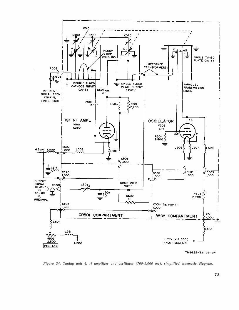
Figure 34. Tuning unit 4, rf ampiifier and oscillator (700-1,000 mc), simplified sthematic diagram.
73
which is anchored to the secondparal lel 1/2-wavelength transmis-sion line. Pins 2 and 3 of the tubeare not used. The heater (pins 1and 6) and the cathode (pin 7) ares e c u r e d to supporting metallicclamps which prevent mechanicalvibration and provide secure elec-trical contact to the following po-tentials required for tube opera-tion:
(a) Heater voltage is connected fromthe power supply through feed-through capacitor C540, whichpenetrates the chassis wall thate n c 1 o s e s the crystal diodeC R 5 0 1 c o m p a r t m e n t . A w i r elead conducts the heater voltageto a second feedthrough capac-i to r , C558 , which i s inse r t edthrough the common wall thatseparates the crystal diode com-partment from the fixed resistorR505 compartment (fig. 34). Asecond wire lead continues theconduction path to the inner ter-minal of feedthrough capacitorC512, which isolates the 6.3-voltheater l ine from the groundedwall and is connected to rf chokeL506, which is mounted withinthe oscillator cavity. Choke L506is connected to the heater (pin 1)of V502. The 6.3-volt return pathis through pin 6 of V502 and rfchoke L507 to chassis ground.
(b) The bias for oscillator V502 isdeveloped by the voltage dropacross grid resistor R504. Thecathode (pin 7) has a dc returnpath to chassis ground throughrf choke L507.
(c) The B+, 105-volt dc potential isapplied to the plate of the oscil-lator tube only when the bandselector is rotated to the 700-1,000-mc position. This potentialis applied through two rf chokesand two feedthrough capacitors.The first choke, L522, is outsideof the tuner chassis and is inseries with the switch terminalon band selector S503 that applies
B+ potential to oscillator V502.Feedthrough capacitor C511 pen-etrates the exterior chassis wallthat encloses the resistor R505compartment (A, fig. 74). The B+voltage is reduced by R505 to theproper value for tube operation.The low-po ten t i a l t e rmina l o fR505 is connected to feedthroughcapacitor C509. This capacitorserves two functions: i t pene-trates the interior wall that sep-a ra tes the R505 compar tmentf rom the osc i l l a to r cav i ty ; i tsimultaneously bypasses rf cur-rents in the B+ supply to chassisground. The B+ voltage is appliedthrough rf choke L508 to the plate(pin 4) of the oscillator tube.
52. Rf Tuner, 700-1,000 Mc, DynamicCircuit Analysis
(fig. 34)
The rf incoming signal is applied to adouble-tuned quarter-wavelength shortedcoaxial line type of cavity at the input torf amplifier V501. The signal is increasedin magnitude by the amplifier and is fedto a s i n g 1 e-tuned quarter-wavelengthshorted coaxial line type of cavity in theplate output circuit of V501. An impednace-matching transformer couples the platecavity signal into crystal mixer CR501.An osci l lator which uses a tuned half-wavelength parallel transmission line alsoinjects i ts s ignal into the crystal mixerinput. As a result of heterodyning actionwithin the crystal mixer, sum and differ-ence frequencies are produced. Since theif. preamplifier is tuned to the differencefrequency, t h i s h e t e r o d y n e d s i g n a l i spassed on to the if. amplifiers for ampli-fication, and to the detector and electro-meter circuit for metering and audio signaldetection.
a. V501 Input Circuit . T h e i n c o m n gsignal is coupled into the first coaxial-typecathode input cavity at an area of low rfimpedance. A pickup loop is used to trans-fer the rf energy from the f irst to thesecond tuned cavity. Effectively, the tunedcav i t i e s func t ion a s a doub le - tuned r f
74
t ransformer, with optimum coupling be-tween primary and secondary windings.The lengths of the coaxial lines in the inputcircuit are chosen to resonate ( togetherwith the tube interelectrode capacitances)in the 700- to 1,000-mc frequency range.Section A of tuning capacitor C510 loadsthe f i rs t coaxial l ine and provides therequired tuning range; section B of capac-itor C510 serves the same function for thesecond cavity. For vernier tracking of theamplif ier with the osci l lator , a metal l ictab is positioned between the grounded wallof the coaxial-type cavity and the statorplates of tuning capacitor C510, sectionsA and B. Varying the position of the tab,with reference to the stator plates, per-mits trimming the high-frequency end ofthe tuning range during alignment proce-dures. Capacitor C550 is the trimmer tabcapacitor for the first input cavity; C560is the trimmer for the second input cavity.Energy transfer from the second cavity tothe cathode of the grounded-grid amplifieris obtained by coupling capacitor C501,which i s connec ted be tween the s t a to rplates of tuning capacitor C510B and theconduc t ive tube c l ip tha t suppor t s t hecathode of amplifier V501.
b. V501 Output Circuit. The amplif iedrf signal at the plate of amplifier V501 iscoupled from the conductive metallic tubecl ip that secures the plate of the tubethrough a second tubular capacitor, C507,to the s tator plates of tuning capaci torC510, section C. This section of the cavity,which includes the plate of the amplifierand capacitor section C510C, constitutesthe th i rd shor t ed coax ia l l i ne o f 1 /4 -wavelength tuning range. Similar to thefirst two tuned cavities (a above), C510Cloads the s ingle-tuned coaxial l ine andprov ides a tun ing r ange f rom 700- to1,000-mc; C570 is the trimmer tab capac-itor provided for alignment at the high-frequency end of the band. A loop, posi-tioned near the low rf impedance area inthe tuned cavity, injects the amplified rfsignal into the crystal mixer CR501 inputcircuit . This loop functions as an im-pedance-matching transformer to matchthe input impedance of diode CR501, whichis in the order of 200- to 300-ohms.
c. V502 Oscillator Circuit. A capacity-loaded half-wavelength pair of paralleltransmission lines is used in the oscillatorcircuit. The lines are connected betweenthe plate and grid of V502 and are properlydimensioned to sustain oscillations overthe required tuning range, which is 42-mchigher than the incoming rf signal. SectionD of tuning capacitor C510, mechanicallyganged with the amplifier sections, pro-vides the tracking frequency range from742- to 1,042-mc. Because of the con-structional difference between the ampli-fier and oscillator tuned lines, no metallictrimmer tab capacitor is required for theoscillator circuit. A loop, positioned in theoscillator cavity, functions as an imped-ance-matching transformer to inject os-cillator voltage into the input circuit ofcrystal mixer CR501.
d. Crystal Mixer Circuit. The nonlinearcharacteristics of a crystal diode, CR501,are utilized for the heterodyning processbecause of the favorable s ignal- to-noiseratio obtained at the ultrahigh frequenciesof tuning unit 4 . The diode produces anumber of frequencies at its output. Theseare the two original signal and oscillatorfrequencies ( tracked 42-mc apart) , andthe i r sum and d i f fe rence f requenc ies .Crystal mixer coil L505 is resonated to42 mc and the i f , p reampl i f i e r c i r cu i ti s p re tuned to 42 mc ; the re fo re , on lythe difference frequency is passed throughou tpu t t e rmina t ion CP501 and a shor tlength of coaxial cable to connector jackJ507 on the 42-mc if. amplifier subassem-bly. All other frequencies are bypassedto ground through capacitor C508, whichis connected to the input terminal of signalpeaking coil L508 within the crystal diodecompartment of the rf tuner.
53. Rf Tuner, 400-700 Mc, Introduction(fig. 35)
With the front-panel band selector ro-tated to the 400-700-mc position, the signalvoltage from the main unit is connectedfrom coaxial switch S501 by cable assem-bly W503 and its connector plug P503 tomating jack J508 on the exterior of the400-700-mc rf tuner.
75
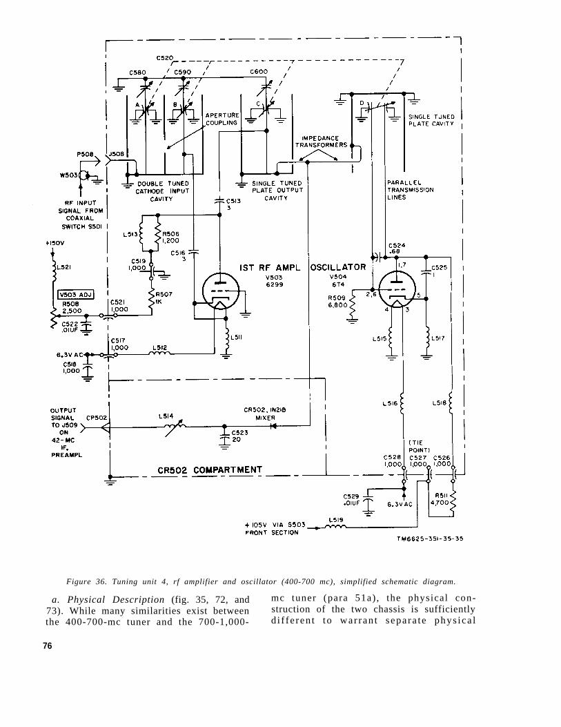
Figure 36. Tuning unit 4, rf amplifier and oscillator (400-700 mc), simplified schematic diagram.
a. Physical Description (fig. 35, 72, and mc tuner (para 51a), the physical con-73). While many similarities exist between struction of the two chassis is sufficientlythe 400-700-mc tuner and the 700-1,000- d i f fe rent to war rant separate phys ica l
76
descript ions. At r i ca l d iag ram
combined physical-elec-of the 400-700-mc tuner
(fig. 35) shows that rf amplifier V503 andoscillator V504 are housed in a chassisthat contains four tuned coaxial-type cav-i t ies and one rectangular compartment.Th i s chass i s i s a l so cons t ruc ted wi threlatively thick walls to provide mechan-ical stability and electrical isolation. Twocovers (fig. 72) are secured to the chasis.One i s snug ly secured to the ex te r io rs ide and p rov ides sh ie ld ing aga ins t r fleakage for the amplifier cavities and theoscillator cavity. A second cover, of Z-shape construction, is secured to the com-partment that houses crystal diode CR502and crystal mixer coil L514. The tuningslug of the mixer coil projects through avert ical wall of the crystal diode com-partment; this s lug is factory set for af lat frequency response over the band.Reference to the parts location diagram(fig. 73) shows that five feedthrough ca-pacitors (C517, C521, C526, C527, andC528), a right-angle input signal connector(J508), and a termination (CP502) for theoutput signal cable are inserted throughthe tuner walls for purposes described inb below.
b. Circuit Analysis , Stat ic Condit ion.The 400-700-mc rf tuner consists of fiveseparately confined but funct ional ly in-terrelated circuits with operating voltagesfor the tube electrodes applied as follows:
(1) Amplif ier circuit . Similar to the700-1,000-mc tuner (para 51b(1)),t h e a m p l i f i e r c i r c u i t u s e s aground e d-grid coplanar t r iode,V503 (fig. 35 and 73). The grid diskis secured to the grounded partitionthat separates the cathode inputcavity from the plate output cavity;this avoids the need for neutraliza-tion of the amplifier input circuitand minimizes the generat ion ofspurious frequencies.
(a) Heater voltage is connected fromthe power supply, through feed-through capacitor C517 (B, fig.73) and rf choke L512, to one ofthe heater pins. The return pathfor the heater voltage is throughrf choke L511 to chassis ground.
(b)
Feedthrough capacitor C518 de-couples rf currents in the heatercircuit from the power supply.The p la te cu r ren t o f the type6299 amplifier tube must be lim-ited to a maximum of 10 milli-amperes to prolong the life of thecoplanar tr iode tube. Variableresistor R508, designated V503ADJ, is provided for this adjust-ment. Rf choke L521 applies the+150-volt output of the powersupply to one terminal of R508,which is mounted outside of thecavity on the tuning unit framea s s e m b 1 y (fig. 72). CapacitorC521 penetrates the cavity walland connects the B+ potentialthrough voltage-dropping resis-tor R507 (B, f ig. 73) to feed-through capacitor C519, which ismounted on a supporting bracket(A, fig. 73) in the plate cavity.The b racke t se rves as a con-venient anchoring point for oneterminal of rf choke L513, whichis wound on R506. The secondte rmina l o f r f choke L513 i ssoldered to the underside of themetallic tube clip which supportsamplifier tube V503 within thecavity. Rf choke L513 connectsthe B+ potential to the plate elec-trode of V503 and offers a highimpedance to rf currents in theplate circuit. Capacitor C513, oftubular construction, is also sol-de red to the under s ide o f theplate tube clip, and offers a low-impedance path for rf energy topass to the tuned plate outputcavity.
(2) Oscil lator circuit . The osci l latorconsists of a miniature-type 6T4triode connected to two parallel1/2-wavelength c a p a c i t y-loadedtransmission lines (A, fig. 73). Thelength of the parallel transmissionlines must be greater than thosein the 700-1,000-mc tuner so thatre sonance can be ob ta ined overthe 400-700-mc tuning range. Fort h i s r e a s o n , the large-envelope
77
acorn-type electron tube cannot beutilized, and a smaller envelope-type 6T4 tube is employed. Oper-ating potentials are applied to theterminals at the base of the tubesocket as follows:
(a)
(b)
(c)
Heater voltage is connected fromthe power supply through feed-through capacitor C528 (A, fig.73) which penetrates the oscil-lator compartment. Bypass ca-pacitor C529 decouples rf energyin the heater circuit from theheater power supply line. A shortlength of wire connects the heatervoltage through rf choke L516to one side of V504 heater (pin 4).The heater voltage return path isthrough rf choke L515 to chassisground.Grid bias for oscillator V504 isdeveloped by the voltage dropacross grid resistor R509. Thec a t h o d e (pin 5) is connectedthrough rf choke L517 to chassisground.The 105-volt dc potential is ap-plied to the plate (pins 1 and 7)of the oscillator tube only w h e nthe f ron t pane l band se l ec to r(S503) is rotated to the 400-700 -mc position. The dc potential isapplied through two rf chokes,two feedthrough capacitors, andone res i s to r . The f i r s t choke ,L519, is outside of the rf tunerand in series with terminal 2 onband selector S503 (front sec-tion) which applies B+ potentialto V504. Feedthrough capacitorC527 penetrates the c h a s s is;however, this capacitor servesonly as a convenient tie point foranchoring one terminal of cur-r en t - l imi t ing r e s i s to r R511 tothe exterior of the chassis (A,fig. 73). The B+ voltage is de-creased by fixed resistor R511 tothe proper value for tube opera-t ion. The low-potential s ide ofR511 is connected to feedthroughcapacitor C526 which penetratesthe exterior wail of the oscillator
cavity and serves as an rf bypass.The B+ voltage is applied throughrf choke L518 to the plate (pins1 and 7) of the oscillator tubeand to one of the l/2-wavelengthpa ra l l e l t r ansmiss ion l ines inthe oscillator plate circuit. Thesecond parallel transmission lineoperates at dc ground potential.
54. Rf Tuner, 400-700 Mc, DynamicCircuit Analysis
(fig. 35)
The dynamic circuit analysis for the400-700-mc rf tuner is identical with thatfo r the 700-1 ,000-mc tuner (pa ra 52)except for substitution of applicable refer-ence symbols and the following circuitcomponents:
a. V503 Input Circuit. No pickup loop isemployed for coupling the rf energy fromthe first to the second coaxial-type tunedcavity. Because a pickup loop at the lowerfrequency range of 400- to 700-mc mustbe considerably longer than that employedin the upper frequency band (700-to 1,000-mc), undesirable resonances in the tuningrange can be created. Instead of a pickuploop, an aperture of proper dimensions forthe pass band of the frequencies desired iscut into the wall separating the first andsecond input tuned cavities. This aperturemethod of coupling permits ample transferof rf energy from the first to the secondinput cavity. Except for the difference incoupling methods, V503 amplifier employsre fe rence symbol C520 as the gangedtuning capacitor. Metallic tab capacitorsC580 and C590 permit vernier tracking ofthe amplifier and oscillator sections of thetuning capacitor.
b. V503 Output Circuit . Section C oftuning capaci tor C520 loads the s ingle-tuned coaxial line in the amplifier outputcircuit. Metallic tab capacitor C600 servesthe same function as metallic tab capac-itor C570 for the 700-1,000-mc rf ampli-f i e r .
c. V504 Oscillator Circuit. Section D oftuning c a p a c i t o r C250, mechanicallyganged with amplifier sections A, B, andC of C520, provides the tracking frequency
78
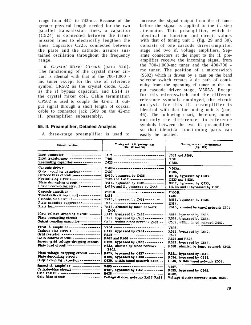
Figure 29. Figure 102.
range from 442- to 742-mc. Because of thegreater physical length needed for the twoparal lel t ransmission l ines, a capacitor(C524) is connected between the trans-mission lines to electrically lengthen thelines. Capacitor C225, connected betweenthe plate and the cathode, assures sus-tained oscillation throughout the frequencyrange.
d. Crystal Mixer Circuit (pa ra 52d) .The functioning of the crystal mixer cir-cuit is idential with that of the 700-1,000 -mc tuner except for the use of referencesymbol CR502 as the crystal diode, C523as the rf bypass capacitor, and L514 asthe crystal mixer coil. Cable terminationCP502 is used to couple the 42-mc if. out-put signal through a short length of coaxialcable to connector jack J509 on the 42-mcif. preamplifier subassembly.
55. If. Preamplifier, Detailed Analysis
A three-stage preamplif ier is used to
increase the signal output from the rf tunerbefore the signal is applied to the if. stepattenuator. This preamplifier , which isidentical in function and circuit valueswith that of tuning unit 3 (fig. 29 and 30),consists of one cascode driver-amplif ierstage and two if. voltage amplifiers. Sep-arate connectors at the input to the if. pre-amplifier receive the incoming signal fromthe 700-1,000-mc tuner and the 400-700 -mc tuner. The position of a microswitch(S502) which is driven by a cam on the bandselector switch creates a dc path of conti-nuity from the operating rf tuner to the in-put cascode driver stage, V505A. Exceptfo r th i s mic roswi tch and the d i f f e ren treference symbols employed, the circuita n a l y s i s f o r t h i s i f . p r e a m p l i f i e r i sidentical with that for tuning unit 3 (para46). The following chart, therefore, pointso u t o n l y t h e d i f f e r e n c e s i n r e f e r e n c esymbols between the two if. preamplifiersso that identical funct ioning parts caneasily be located.
79
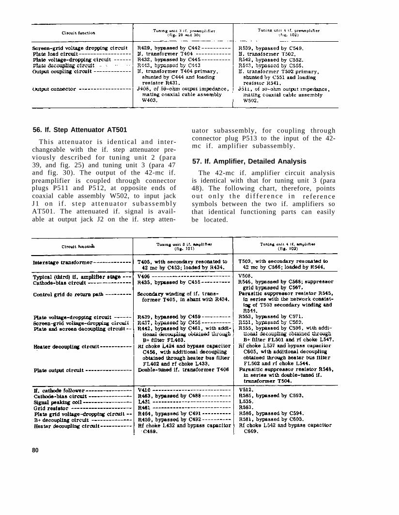
Figure 102.Figure 29.
Figure 101. Figure 102.
56. If. Step Attenuator AT501
This at tenuator is identical and inter-changeable with the if. step attenuator pre-viously described for tuning unit 2 (para39, and fig. 25) and tuning unit 3 (para 47and fig. 30). The output of the 42-mc if.preamplifier is coupled through connectorplugs P511 and P512, at opposite ends ofcoaxial cable assembly W502, to input jackJ1 on i f . s t ep a t t enua to r subassemblyAT501. The attenuated if. signal is avail-
uator subassembly, for coupling throughconnector plug P513 to the input of the 42-mc if. amplifier subassembly.
57. If. Amplifier, Detailed Analysis
The 42-mc if. amplifier circuit analysisis identical with that for tuning unit 3 (para48). The following chart, therefore, pointso u t o n l y t h e d i f f e r e n c e i n re fe rencesymbols between the two if. amplifiers sothat identical functioning parts can easily
able at output jack J2 on the if. step atten- be located.
80
Figure 102.Figure 101.
58. Detector and Electrometer Circuit A501 channels, and applies output signals to the(fig. 19) appropr i a t e c i r cu i t s i n the ma in un i t .
All tuning units employ an identicalsealed detector and electrometer circuit.Each circuit accepts driving power fromthe if. amplifier, detects the signal in sep-a ra te a u d i o a n d d c m e t e r i n g s i g n a l
These sealed circuits are interchangeablewith each other and perform the functionsdescribed in detail for detector and elec-trometer circuit A1 within tuning unit 1(para 32 and 33).
Section VII. THEORY OF MINOR
59. Minor Components for Use withTuning Unit 1
Five minor components are supplied foruse with tuning unit 1. A physical descrip-tion of these components is given in TM11-6625-351-12. The fo l lowing c i rcu i tanalysis supplement the information con-tained in TM 11-6625-351-12.
a. Antenna AT-1029/URM-85. This loopantenna (fig. 36) consists of a single turnof wire and a base which houses matchingtransformers, an injection network for theimpulse genera to r s igna l , and a bandswitch to select one of the six bands cor-responding in frequency to that inscribedon the front panel of tuning unit 1. Theloop itself consists of a single turn of wireenclosed in an electrostatic shield. There-fore, the loop is relatively insensitive tothe e l ec t r i c f i e ld componen t o f r ad ioenergy but is highly responsive to themagnetic field component. Because of thesingle turn of wire in the loop itself, thisantenna has an extremely low-output im-pedance match.
(1) Rf signal path. To match the out-put impedance of the loop antennato the r ed co lo r -coded 50-ohmcharac te r i s t i c impedance o f themating c o a x i a l r f c a b l e , f o u rmatching t rans fo rmers , T1001t h r o u g h T 1 0 0 4 , a r e u s e d . T h et rans fo rmers , o f s u b m i n i a t u r econstruction, are enclosed in fer-
(2)
COMPONENTS
r i t e cup co res to ob ta in p ropershielding f r o m stray magneticfields. The proper step-up ratio isobtained by rotating band switchS1001, at the front of the housing,to the same frequency band in useby tuning unit 1. For band 5 (5.2-to 12.7-mc) and band 6 (12.7- to30-mc) , the loop impedance i sclose to 50-ohms and no step-uptransformer is required.Impulse generator signal p a t h.When the loop antenna over the fre-quency range of tuning unit 1 isused, calibration of the test set isaccomplished by injecting a voltagef r o m t h e i m p u l s e g e n e r a t o r i nseries with the secondary windingof the se lec ted ma tch ing t r ans -former. For bands 5 and 6, sectionC of switch S1001 conducts the im-pu l se gene ra to r s igna l in se r i e swith the loop itself. Sections A andB of the switch then provide a dcpath to output connector J1001. Theimpulse generator signal path isfrom the main unit IMPULSE OUT-PUT front-panel jack, through thegreen color-coded mating rf cableto the injection network built intothe green color-coded signal con-nector J1002. When the calibratingvoltage from the impulse generatorcircuit is injected in series with theincoming rf signal, the calibrating
81
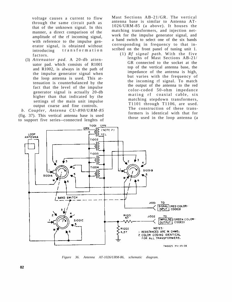
(3)
voltage causes a current to f lowthrough the same circuit path asthat of the unknown signal. In thismanner, a direct comparison of theamplitude of the rf incoming signal,with reference to the impulse gen-erator signal, is obtained withoutintroducing t r a n s f o r m a t i o nfac to r s .At tenua tor pad . A 20-db a t t en -uator pad. which consists of R1001and R1002, is always in the path ofthe impulse generator signal whenthe loop antenna is used. This at-tenuation is counterbalanced by thefact that the level of the impulsegenerator signal is actually 20-dbhigher than that indicated by thesettings of the main unit impulseoutput coarse and fine controls.
b . Coupler , An tenna CU-890/URM-85(fig. 37). This vertical antenna base is usedto support five series--connected lenghts of
Mas t Sec t ions AB-21/GR. The ver t i ca lantenna base is similar to Antenna AT-1026/URM-85 (a above). I t houses thematching transformers, and injection net-work for the impulse generator signal, anda band switch to select one of the six bandscorresponding in frequency to that in-scribed on the front panel of tuning unit 1.
(1 ) Rf s igna l pa th . W i t h t h e f i v elengths of Mast Sections AB-21/GR connected to the socket at thetop of the vertical antenna base, theimpedance of the antenna is high,but varies with the frequency ofthe incoming rf signal. To matchthe output of the antenna to the redco lo r -coded 50-ohm impedancem a t i n g r f c o a x i a l c a b l e , s i xmatching stepdown transformers,T1101 through T1106, are used.The construct ion of these trans-formers is identical with that forthose used in the loop antenna (a
Figure 36. Antenna AT-1026/URM-86, schematic diagram.
82
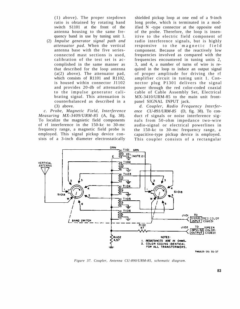
(2)
(1) above). The proper stepdownratio is obtained by rotating bandswitch S1101 at the front of theantenna housing to the same fre-quency band in use by tuning unit 1.Impulse generator signal path andattenuator pad. When the verticalantenna base with the five series-connected mast sect ions is used,cal ibrat ion of the test set is ac-complished in the same manner asthat described for the loop antenna(a(2) above). The attenuator pad,which consists of R1101 and R1102,is housed within connector J1102and provides 20-db of attenuationt o t h e i m p u l s e g e n e r a t o r c a l i -brating signal. This attenuation iscounterbalanced as described in a(3) above.
c. Probe, Magnetic Field, InterferenceMeasuring MX-3409/URM-85 (A, fig. 38).To localize the magnietic field componentsof rf interference in the 150-kc to 30-mcfrequency range, a magnetic field probe isemployed. This signal pickup device con-sists of a 3-inch diameter electrostatically
shielded pickup loop at one end of a 9-inchlong probe, which is terminated in a mod-ified N -type connector at the opposite endof the probe. Therefore, the loop is insen-i t ive to the electr ic f ield component ofradio interference signals , but is highlyresponsive t o t h e - m a g n e t i c f i e l dcomponent. Because of the reactively lowfrequencies involved as compared with thefrequencies encountered in tuning units 2,3, and 4, a number of turns of wire is re-quired in the loop to induce an output signalof proper ampli tude for driving the rfamplif ier circui t in tuning unit 1. Con-nec to r p lug P1301 de l ive r s the s igna lpower through the red color-coded coaxialcable of Cable Assembly Set, ElectricalMX-3410/URM-85 to the main unit front-panel SIGNAL INPUT jack.
d. Coupler, Radio Frequency Interfer-ence CU-891/URM-85 (D, fig. 38). To con-duct rf signals or noise interference sig-na l s f rom 50-ohm impedance two-wi reaudio-signal or electr ical powerl ines inthe 150-kc to 30-mc frequency range, acapacitive-type pickup device is employed.Th i s coup le r cons i s t s o f a r ec tangu la r
Figure 37. Coupler, Antenna CU-890/URM-85, schematic diagram.
83
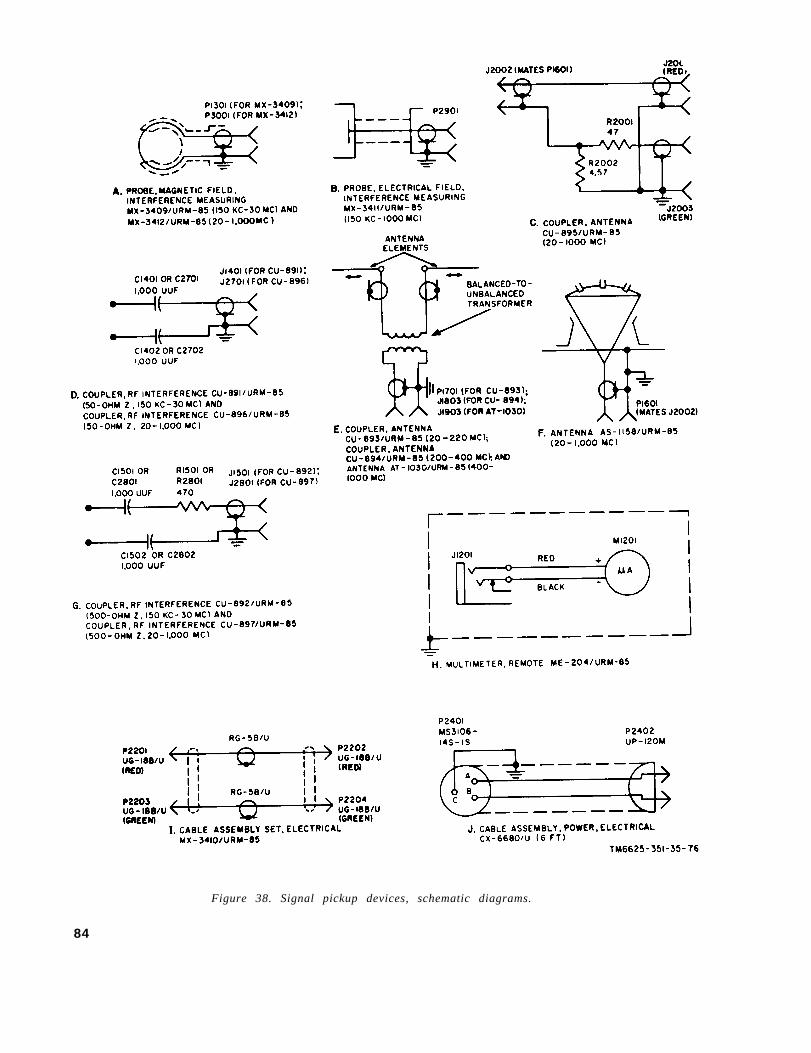
Figure 38. Signal pickup devices, schematic diagrams.
84
hous ing which has two sp r ing- loadedbinding posts at one end and an N-type con-nector at the opposite end. The uninsulatedends of two wire leads, which are con-nected to the audio or powerline at theiropposite ends, are inserted into the bindingposts. Any dc voltage present on the linesunder measurement is blocked by couplingcapacitors C1401 and C1402. The rf signalat connector jack J1401 is coupled throughthe red color-coded coaxial cable of CableAssembly Set, Electrical MX-3410/URM-85 to the main unit SIGNAL INPUT jackfor amplif icat ion, detect ion, and meterpresentat ion.
e. Coupler, Radio Frequency Interfer-e n c e C U - 8 9 2 / U R M - 8 5 (G, fig. 38). Toconduct rf s ignals or noise interferencesignals from approximately 500-ohm im-pedance two-wire audio-signal or elec-trical powerlines in the 150-kc to 30-mcfrequency range, another capacitive-typepickup device is employed. Similar in con-struction and function to the CU-891/URM-85 (d above), this coupler has one addi-tional circuit component. Resistor R1501,in series with the ungrounded lead fromthe audio-line or powerline coupling ca-pacitor C1501, serves as an impedance-matching device. Effectively, it convertsthe approximate 500-ohm input line to a50-ohm coaxial cable jack J1501 to the50-ohm impedance so that maximum powertransfer from connector jack J1501 to the50-ohm coaxial cable can be effected.Again, the red color-coded coaxial cableof Cable Assembly Set , Electrical MX-3410/URM-85 conducts the rf signal to themain unit front-panel SIGNAL INPUT jackfor amplif icat ion, detect ion, and meterpresentat ion.
60. Minor Components for Use with TuningUnits 2, 3, and 4
(fig. 38)
a. Antenna AS-1158/URM-85 The dis-cone (broadband) antenna (F, fig. 38) isused as a nondirectional, relatively con-stant impedance antenna over the wide fre-quency range from 20 to 1,000 mc withtuning units 2, 3, and 4. In operation, itis mounted on the AT-1027/URM-85, which
functions as a counterpoise to s imulateearth ground. At the curved top surface ofthe cone, three sockets are provided toa c c e p t t h e s p e c i f i c n u m b e r o f M a s tSec t ions (AB-21 /GR) requ i red fo r r es -onating with the rf signal under measure-ment, as illustrated in TM 11-6625-351-12. The rf signal is conducted from thebase of the sockets within the antennahousing by a wire post to the modified N-type terminating connector P1601 at thebase of the cone-shaped structure. Theo u t s i d e s h e l l o f c o n n e c t o r P 1 6 0 1 i sgrounded through the unbalanced injectionblock (Coupler, Antenna CU-895/URM-85)and the rf cables to the ground potentialof the main unit panel.
b. C o u p l e r, Antenna CU-895/URM-85(C, fig. 38). This coupler, housed in anirregular-shaped metal and plast ic con-tainer, is provided as a means of couplingthe output of Antenna AS-1158/URM-85(a above) to the test set. One connectorjack, J2002, located at one end of thecoupler, mates the N-type connector plug,P1601, which terminates the base of thebroadband antenna. Two connector jacks,J2001 and J2003, are located adjacent toeach o the r a t t he oppos i t e end o f thecoupler . These connec to r s func t ion asfollows:
(1)
(2)
Rf s i g n a 1 path connector J2001.The rf signal is coupled from inputconnector J2002 direct to rf outputconnector J2001. The red color-coded coaxial cable of Cable As-sembly Set, Electrical MX-3410/URM-85 interconnects output jackJ2001 to the main unit front-panelSIGNAL INPUT jack . S ince theouter shell of the SIGNAL INPUTjack is at chassis ground potential,the outer shell of jack J2001 andt h e c o u n t e r p o i s e a r e a l s o c o n -ducted through to ground potential.The rf signal is conventionally am-plified and detected in the test setf o r p r e s e n t a t i o n o n t h e p a n e l -mounted meter.I m p U 1 s e generator signal pathconnector J2003. When the broad-band antenna over the frequencyrange from 20 to 1,000 mc is used,
85
calibration of the test setcomplished by inject ing a
i s a c -Signal
from the impulse generator to theattenuator network housed in thecoupler . The signal path is fromthe main unit IMPULSE OUTPUTfront-panel jack, through the greenco lo r -coded cab le o f Cab le As-sembly Set, Electrical MX-3410/URM-85 and connector jack J2003.The ca l ib ra t ing vo l t age i s thena p p l i e d t o a 1 0 - t o - 1 v o l t a g e -divider network which consists ofR2001 shun ted by R2002 ; t h i sresults in a 20-db signal loss. Thecalibrating signal from the impulsegenera to r c i r cu i t i s i n j ec ted inseries with the incoming rf signal(identical with the method used inloop antenna and the vertical an-tenna and the vertical antenna, para59a and b). Therefore, the cali-brating voltage causes a current toflow through the same circuit pathas that of the unknown signal. Inthis manner, a direct comparisonof the amplitude of the rf incomingsignal , w i t h r e f e r e n c e t o t h eimpulse generator s ignal , is ob-tained without introducing trans-formation factors.
c. C o u p l e r Antenna CU-893/URM-85(E, f ig. 38). Coupler Antenna CU-893/URM-85 is used for picking up radiatedsignals over the frequency range from 20to 220-mc (corresponding to the range oftuning unit 2). It consists of a phenolic tubewhich functions as a supporting boom, ablock assembly at one end of the boom, anda b a l a n c e d - t o - u n b a l a n c e d t r a n s f o r m e r(balun) at the opposite end of the boom, thepurpose of the block assembly is to serveas a means of physical at tachment andelectrical connection for the two arms of atelescopic dipole antenna. The purpose ofthe balun is to convert the balanced inputfeeding system, which consists of the twodipole arms, into an unbalanced feed whichconsists of the single coaxial terminatingconnector P1701.
(1) Balanced input system B a l a n c e doutput frowm the center of the an-t enna i s f ed th rough a pa i r o f
(2)
coaxial cables, onearm, to the balun.
for each dipoleThe input side
of the balun is also balanced sothat both arms of the antenna s e ethe same impedance. The length ofthe coaxial cables is cr i t ical foroptimum phasing and a low voltagestanding wave ratio over the fre-quency band. Since the phenolicboom is too short for a straightrun of coaxial cables over the 20-to 220-mc band , the r emain inglengths of the cables are wound ona bakelite form within the balunhousing.Unbalanced output connector. E s-sentially, the actual coupling be-tween the input and output cir-cuits consists of two 1-turn loopsof wire coupled together. The rfenergy from the balanced coaxialcables is coupled into the N-typeoutput connector , P1701, whichmates with the input end of the redco lo r -coded cab le o f Cab le As-sembly Set, Electrical MX-3410/URM-85. The far end of this cableapplies the rf signal to the mainunit SIGNAL INPUT jack for ampli-ficiation, detection, a n d m e t e rPresentation on the test set.
d. Coupler, Antenna CU-894/URM-85(E, f ig. 38). Coupler, Antenna CU-894/URM-85 is used for picking up radiatedsignals over the frequency range from 200-to 400-mc (corresponding to the range oftun ing un i t 3 ) . Th i s coup le r func t ionsidentical ly with the CU-893/URM-85 (cabove). At one end of the boom, its blockassembly i s phys ica l ly cons t ruc ted o fplexiglass instead of phenolic material ;in addit ion, the CU-894/URM-85 outputconnector at the balun end of the boom isdesignated reference symbol J1803.
e. Antenna AT-1030/URM-85. AntennaAT-1030/URM-85 is used for picking upradiated signals over the frequency rangefrom 400- to 1,000-mc (corresponding tothe range of tuning unit 4). Although thisantenna is not shown in figure 38, it isidentical in cirouit analysis with the CU-893/URM-85 (C above) and the CU-894/URM-85 (d above) except for the addition
86
of a 90° ang le corner r e f l ec to r . Th i sreflector, illustrated in TM 11-6625-351-12, provides a power gain of approximately10-db throughout its frequency range. Toobtain a proper impedance match to thetwo 50-ohm coaxial cables that connect thedipoles (at one end of the boom) to thebalun (at the opposite end of the boom), anan tenna impedance o f 100-ohms i s r e -quired. This impedance is obtained with adipole-to-reflector corner spacing of 0.4wavelength. Since the wavelength changesas the test set is tuned to various fre-quencies in the 400- to 1,000-mc range,the spacing between the dipoles and thecorner of the reflector must be adjusted.One side of the megacycle ruler, suppliedas a minor component , is cal ibrated toindicate the proper spacing between theplane of the dipoles and the corner of thereflector; the other side of the ruler iscal ibrated to indicate the proper lengthof each d ipo le a rm fo r the pa r t i cu la rf r e q u e n c y u n d e r m e a s u r e m e n t . E a c hdipole is of telescopic construct ion andmay be extended from its minimum col-lapsed length of 2-1/4 inches to a max-imum 1 e n g t h of approximately 6-1/2inches.
f . Probe Magnetic Interference Meas-uring MX-3412/URM-85 (A, fig. 38). Themagnetic field probe is used to localizemagnetic f ield components of rf inter-ference in the 20- to 1,000-mc frequencyrange. This signal pickup device is iden-tical in function with the MX-3409/URM-85 (para 59c) which is used for the 150-kc to 30-mc frequency range. Because oft h e h i g h e r f r e q u e n c y e l e c t r o m a g n e t i cfields employed, only 1 turn of wire in theloop end of the probe is required. Con-nector plug P3001 mates the red color-coded coaxial cable of Cable AssemblySet, Electrical MX-3410/URM-85, so thatthe path of continuity to the main unit SIG-NAL INPUT jack is completed.
g. Coupler, Radio Frequency Interferw-ence CU-896/URM-8S (D, fig. 38). The CU-896/URM-85 (a capacit ive-typd pickupdevice) is used to conduct rf signals ornoise interference signals from 50-ohmimpedance 2-wire audio-signal or elec-trical powerlines in the 20- to 1,000-mc
frequency range. The CU-896/URM-85 isidentical in function with the CU-891/URM-85 (para 59d), but differs in the fol-lowing physical respects:
h. Coupler, Radio Frequency Interfer-ence CU-897/URM-85 (G, fig. 38). T h eCV-897/URM-85 (another capacitive typepickup device) is used to conduct rf sig-nals or noise interference from approxi-mate 500-ohm impedance 2-wire audio-s igna l o r e l ec t r i ca l power l ines in the20- to 1,000-mc frequency range. Thiscoupler is identical in function with theCU-892/URM-85 (para 59e), but differs inthe following physical respects:
61. Minor Electrical Components forUse with All Tuning Units
(fig. 38)
a. P r o b e, Electrical Field, Intelfer-ence Measuring MX-3411/URM-85(B, f ig.38). The electrical field probe is used tolocalize the electric field component of rfinterference over the complete frequencyrange of the test set from 150-kc to 1,000-mc. This signal pickup device consists of
87
a phenolic tube, approximately 8 incheslong by 7/8 inch diameter, with a N-typeconnector at one end, and with a rubberfunnel to protect the operator from acci-dental contact with high voltage. The op-posi te end of the device is the closedphenolic end of the tube, which protectsthe uninsulated end of a 6-inch length ofNo. 14AWG bus bar. Since no electro-stat ic shield is used on the device, theapproximate 1/4-inch length of uninsu-lated bus bar wire functions as a pickupfor the e l ec t r i c f i e ld componen t o f r fnoise s ignals . The signal is conductedto the test set by connecting the red color-coded cable of Cable Assembly Set, Elec-t r i ca l MX-3410/URM-85 be tween theprobe connector, P2901, and the main unitSIGNAL INPUT jack. The signal is con-ventionally amplified, detected, and pre-sen ted on the t e s t s e t pane l -moun tedmeter for relative indications of electricfield strength or leakage of noise signalsfrom various types of electrical machin-ery and/or electronic ‘equipment.
b. Mul t imeter , Remote ME-204/URM-85 (H, fig. 38). This meter is used whensignal level indications are required ata remote location from the front panel ofthe main unit. The distance from the frontpanel is limited to the 30-foot length ofCord Assembly , E lec t r i ca l CX-4305/U,which interconnects the front panel RE-CORDER EXT METER jack to the remotemeter jack J1201. Inserting one telephoneplug PJ-068, which terminates one end ofthe CX-4305/U, into the main unit RE-C O R D E R E X T M E T E R j a c k r e m o v e smeter mult ipl ier resistor R725 from themete r ing s igna l pa th in the ma in un i t(fig. 8). Inserting the remaining telephoneplug, PJ-068, which terminates the op-posite end of the CX4305/U, creates anew path of continuity for the meteringsignal. The res i s t ance o f mete r move-m e n t M 1 2 0 1 i s s u b s t i t u t e d f o r m e t e rmul t ip l i e r r e s i s to r R725 , and iden t i ca lmeter pointer deflect ions are presentedsimultaneously on both the panel-mountedmeter and the remote meter.
c. Cable Assembly Set, Electrical MX-3410/URM-85 (I, fig. 38). This minor com-ponent consists of two 30-foot lengths
of Cable, Radio Frequency RG-5B/U thatare taped together at frequent intervalsto prevent shifting in their relative posi-t ions. One length of RG-5B/U is termi-na ted in N- type connec to r s P2201 andP2202. Each connector has a red plasticband identifying it as the proper pair forcoupling the rf incoming signal from thesignal pickup device in use to the mainunit front-panel SIGNAL INPUT jack. Thesecond l eng th o f RG5B/U i s a l so t e r -minated in N-type connectors, but thesetwo plugs are designated P2203 and P2204.Each o f these l a t t e r connec to r s has agreen plast ic band identifying i t as theproper pair for coupling the cal ibrat ingsignal from the main unit IMPULSE OUT-PUT jack to the correspondingly color-coded impulse s ignal connector on thethree signal pickup devices that employthe series method of calibrating the testse t .
d. Cable Assembly, Power, ElectricalCX-6680/U (J, fig. 38). This 6-foot lengthof three-conductor cable connects the mainunit front-panel POWER receptacle to asource of power 110-125 volts, 50-400-cps. One end of the ac power cable is ter-mina ted in a th ree - socke t f emale - typeMS3106-14S-1S connector (P2401) andconnects to the front-panel POWER recep-tacle. The other end of this ac power cableis terminated in a two-prong male-typeplug, UP-120M (P2402) and connects toeither a wall receptacle (from which 110-125-volt , 50-400 -cps, 100-volt amperepower is available) or the AC OUTPUTreceptacle on Transformer, Power, Iso-lation and Step-Down TF-248/G. A bat-tery clip, attached to plug UP-120M byan 8 - inch l eng th o f insu la t ed wi re , i sprovided for connect ing the third con-ductor in the ac power cable to conduitor earth ground.
e. C a b l e Assembly, Special Purpose,Electrical B ra n c h e d CX-6681/URM-85(fig. 39). This cable assembly is used toapply operat ing vol tages and to couplesignals to and from the main unit when atuning unit iS being al igned or repaired.The main branch of the cable is 30-incheslong and serves the following functions:
(1) Male connector P901. C o n n e c t o r
88
(2)
P901 is a two-prong male plug thatmates a two-socket female recep-tacle on’ the right wall of the mainunit tuning unit compartment (fig.46). Withdrawal of a tuning unitfrom the tuning unit compartmentopen-circuits microswitch S711;t h i s a c t i o n d i s a b l e s o p e r a t i n gpower from the main unit powertransformer T702 (fig. 6). The con-ductors connected to plug P901serve as a jumper to restore oper-ating power to the main unit trans-former T702. However, the jumperc i rcu i t i s comple ted on ly whenmicroswitches S901 and S902 aredepressed to their closed-circuitposition, as described in (2) and(3) below.Female multipin connector P902.Connec to r P902 cons i s t s o f 18straight single-conductor socketsand 2 coaxial conductor sockets.When P902 is mated with the recep-tacle at the rear of the tuning unitunder measurement, the 18 single-conductor sockets provide a pathof continuity for the ac and dc po-tentials developed in the main unitfor tuning unit operation. Coaxialconductor socket A1 serves as thetermination for the shielded wirethat provides a dc path for the audiosignal developed in the tuning unitto audio detector V701 in the mainunit. Coaxial socket A2 provides apath for the rf signal (which entersthe test set through the main unit)or for the calibrating signal (devel-oped by impulse generator G701 inthe main unit) to the rf tuner sectionwithin the tuning unit. In additionto providing dc paths of continuity,c o n n e c t o r P 9 0 2 s e r v e s a n o t h e rfunction. T h i s f u n c t i o n i s t h eclosing of the contacts of micro-switch S901, which is physicallylocated on the housing for con-nector P902. The plunger of themicroswitch e x t e n d s approx-imately one-half inch beyond theconnector housing. As P902 mateswith its receptacle on the rear ofthe tuning unit, the plunger is de-
(3)
p ressed anda r e s e t t oposition. To
the contacts of S901the i r c losed-c i rcu i tassure that the main
unit power supply operates into itsnormal load, however, the ac in-put powerl ine is s t i l l incompleteunti l the act ion described in (3)below is accomplished.Male m U l t i p i n connector P903.Connec to r P903 cons i s t s o f 18straight single-conductor pins and2 coaxial-conductor plugs. WhenP 9 0 3 i s m a t e d w i t h r e c e p t a c l eJ701, mounted on the inside rearwall of the tuning unit compart-ment, the 18 single-conductor pinsprovide a path of continuity for theac and dc potentials developed inthe main unit for tuning unit oper-ation. Coaxial conductor pin Alserves as the termination for theshielded wire that provides a dcpath for the audio output s ignalfrom the tuning unit to audio ampli-fier V701 in the main unit. Coaxialconductor pin A2 provides a pathfor the rf or calibrating signal fromthe main unit to the rf tuner sectionof the tuning unit. Connector P903s e r v e s one addit ional funct ion,similar to that of P902 ((2) above).This function is the closing of thec o n t a c t s o f m i c r o s w i t c h S 9 0 2 ,which is physically located on thehousing for connector P903. AsP903 mates with main unit recep-tacle J701, the protruding plungerof the microswitch is depressedand the contacts of S902 are set totheir closed-circuit position. WithS901 on connector P902 closed ((2)above), this action completes thejumper circuit across tuning unitcompartment mic roswi tch S711(fig. 6), and the ac input power tothe main unit t ransformer is re-stored. The power supply worksinto its rated load, which consistsof an operating tuning unit.
62. Transformer, Power, Isolation andStep-Down TF-248/G
(fig. 40)a. 120V Position of S802. This external
89
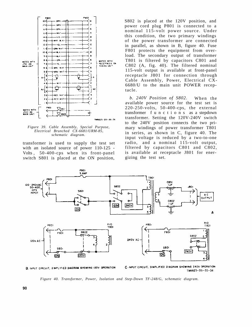
Figure 39. Cable Assembly, Special Purpose,Electrical Brunched CX-6681/URM-85,
schematic diagram.
transformer is used to supply the test setwith an isolated source of power 110-125 -Volts , 50-400-cps when i ts front-panelswitch S801 is placed at the ON position,
S802 is placed at the 120V position, andpower cord plug P801 is connected to anomina l 115-vo l t power source . Underthis condition, the two primary windingsof the power transformer are connectedin parallel, as shown in B, figure 40. FuseF801 protects the equipment from over-load. The secondary output of transformerT801 is filtered by capacitors C801 andC802 (A, fig. 40). The filtered nominal115-volt output is available at front-panelreceptacle J801 for connection throughCable Assembly, Power, Electrical CX-6680/U to the main unit POWER recep-tacle.
b. 240V Position of S802. When theavailable power source for the test set is220-250-volts , 50-400-cps, the externaltransformer f u n c t i o n s as a stepdowntransformer. Setting the 120V-240V switchto the 240V position connects the two pri-mary windings of power transformer T801in series, as shown in C, figure 40. Theinput voltage is reduced by a two-to-oneradio, and a nominal 115-volt output ,f i l tered by capacitors C801 and C802,is available at receptacle J801 for ener-gizing the test set.
Figure 40. Transformer, Power, Isolation and Step-Down TF-248/G, schematic diagram.
90
CHAPTER 2
TROUBLESHOOTING
Section I. GENERAL TROUBLESHOOTING TECHNIQUES
Warning: When servicing the test set, be extremely careful not to contact the B+voltages (from -150 volts to +300 volts dc, and from -300 volts to +150 volts dc). Withac power removed, high dc potentials may still be retained as charges on capacitors.Before touching the exposed parts, be sure that these potentials are removed by shortingthe capacitors to ground. Be especially careful when checking the ac input circuits attieholder XF701 at the terminals of powerline filters FL703 through FL706, at terminalboards TB701 through TB706, and at the terminals of POWER ON-OFF switch S710.
63. General Instructions
Troubleshooting at field and depot main-tenance level includes all the techniquesoutl ined for organizat ional maintenanceand any special or additional techniquesrequired to isolate a defective part. Thefield and depot maintenance proceduresare not complete in themselves, but sup-plement the procedures described in TM11-6625-351-12. The systematic trouble-shooting procedure, which begins with theoperational and sectionalizat ion checksthat can be performed at an organizationall eve l , mus t be comple ted by means o fsect ionalizat ion, local izat ion, and isola-tion techniques.
64. Organization of TroubleshootingProcedures
a. General. The first step in servicing adefect ive test set is to sect ional ize thefault. Sectionalization means tracing thefault to a major component or circuit re-spons ib le fo r abnormal ope ra t ion . Thesecond step is to localize the fault. Local-ization means tracing the fault. to a defec-tive part responsible for the abnormal con-dit ion. Some faults , such as burned-outr e s i s t o r s o r r e c t i f i e r s , a n d a r c i n g o rshorted transformers, often can be locatedby sight, smell, and hearing. The majorityof faults, however, must be localized bychecking voltages and resistances.
b . Sec t iona l i za t ion . The test set con-sists of several units: the various antennas
and probes, the tuning units, the main unit,and the external t ransformer (para 62)when its use is required. The first step intracing trouble is to locate the faulty unitby the following methods:
(1)
(2)
Visual inspection. Visual inspec-tion enables the repairman to lo-cate faults without testing or meas-uring circuits. This inspection isvaluable to avoid additional damagewhich might occur to componentsthrough improper servicing meth-ods, and also to forestal l futuref a i l u r es. The visual inspectionchecks with the power off are givenin TM 11-6625-351-12. With thepower on, visual inspection oftenenab les the r epa i rman to loca tetubes wi th open f i l amen t s , andgassy tubes which give off a bluish-purple glow. All meter readings orother visual s igns should be ob-served and an attempt made to sec-tionalize the fault to a particularunit.Operational tests . Operation a 1tests frequently indicate the gen-eral location of trouble. In manyinstances, the results of the testswill determine the exact nature ofthe fault. The operational checklistin TM 11-6625-351-12 is a goodoperational test.
c. Localization. The tests listed belowwill help to isolate the trouble. First local-ize the trouble to a single stage or circuit,
91
and then isolate the trouble within that cir-cuit by voltage, resistance, and continuitymeasurements .
(1) Resistance measurements. The useof resistance measurements to lo-cate trouble wil l prevent furtherdamage to the equipment if shortcircuits are present. To assist inthe loca l i za t ion o f such f au l t s ,t roubleshooting data include thenormal resistance values as meas-ured at tube sockets and at key ter-minal points . The normal resist-ance values at any point in the mainunit can be determined by referringto the resistance values shown infigures 41 through 45, or by theresistor and capacitor color codes(fig. 96 and 97). Before making anyresistance measurements, turn offthe power and remove the main unitdust cover by following the pro-cedure described in paragraph 40b,item 12, of TM 11-6625-351-12. Aconvenient point for making overallresistance measurements of a tun-ing unit is at the multipin connectorlocated at the rear of the tuningunit chassis. With a tuning unit re-moved f rom the ma in un i t andplaced on the workbench, this con-nector permits a checkout of theproper resistance value for the 20terminals w i t h i n the connectorhousing. If trouble is indicated bylack of correspondence betweenactual measurements taken at themultipin connector and the normalreadings l is ted in paragraph 68,further localization of the troublemust be obtained by measuring re-s i s t a n c e s a t t h e v a r i o u s t u b esockets within the tuning unit. Togain access to the tuning unit tubesockets, remove the tuning unitdust cover as follows:
(a) Remove the four sc rews tha tsecure the rear of the tuning unitdust cover to the tuning unit frameassembly.
(b) Remove the four screws that se-cure the tuning unit dust cover tothe rear of the tuning unit front
(c)
(2)
(3)
(4)
panel. One screw each is locatedat the top, bottom, right, and lefts ides o f t he tun ing un i t dus tcover.Hold the front panel securely andcarefully slide the dust cover offthe tuning unit frame assembly.
Voltage measurements. Most trou-bles ei ther result from abnormalvoltage or they produce abnormalvoltages. Normal voltages at tubesockets and key terminal points inthe main unit are shown in figures41 and 43 through 45. A convenientpoint for measuring power supplyvoltages is at the feedthrough ter-mina l s which p ro jec t f rom thefilter box assembly, mounted on theexterior rear of the main unit (fig.45). Compare the actual readingstaken wi th the normal r ead ingss h o w n . T u b e s o c k e t v o l t a g e sc h e c k s f o r t h e e l e c t r o n t u b e shoused within each tuning unit canbe Wade only by use of Cable As-sembly , Spec ia l Purpose , E lec -trical Branched CX-6681/URM-85(para 61e). In addition, the dustcover of the tuning unit must beremoved ((1) above). Figure 46il lustrates a typical tuning unitoperating outside of its tuning unitcompartment and receiving properac and dc potentials from the re-ceptacle mounted on the rear in-terior wall of the tuning unit com-partment. With a malfunctioningtun ing un i t s e t up a s shown inf igure 46 , compare the vo l t ageread ings t aken wi th the normalr e a d i n g s s h o w n i n f i g u r e s 4 7through 50.Troubleshooting chart. The t r o u-b l e symptoms listed in the chart(para 67) wil l aid in local izingtrouble.Intermittent troubles. In all thesetests, the possibility of intermit-tent troubles should not be over-looked . I f p resen t , t h i s type o ftrouble often can be made to appearby tapping or jarr ing the equip-ment. Check the wiring and con-
9 2
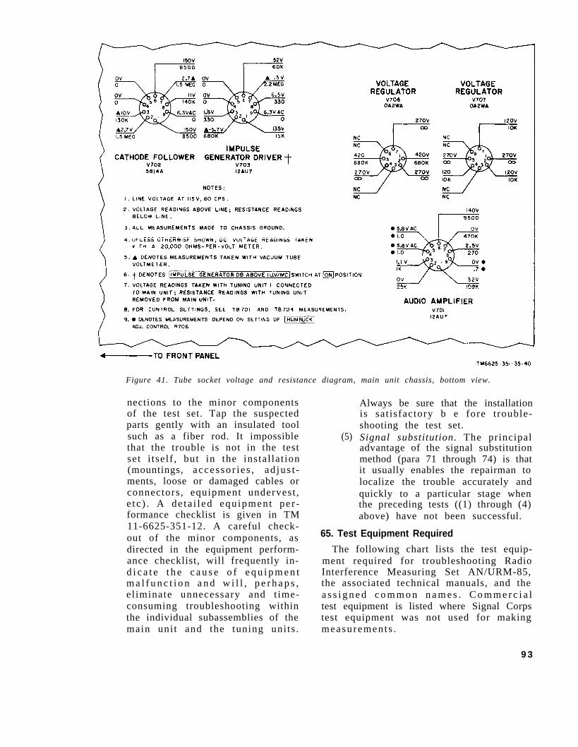
Figure 41. Tube socket voltage and resistance diagram, main unit chassis, bottom view.
nections to the minor componentsof the test set. Tap the suspectedparts gently with an insulated toolsuch as a fiber rod. It impossiblethat the trouble is not in the testset i tself , but in the instal lat ion(mountings, accessor i e s , ad jus t -ments, loose or damaged cables orconnectors , equipment undervest ,e t c ) . A de ta i l ed equ ipment pe r -formance checklist is given in TM11-6625-351-12. A careful check-out of the minor components, asdirected in the equipment perform-ance checklist, will frequently in-d i c a t e t h e c a u s e o f e q u i p m e n tm a l f u n c t i o n a n d w i l l , p e r h a p s ,el iminate unnecessary and t ime-consuming troubleshooting withinthe individual subassemblies of themain uni t and the tuning uni ts .
(5)
Always be sure that the installationis sat isfactory b e fore t rouble-shooting the test set.Signal substitution. The principaladvantage of the signal substitutionmethod (para 71 through 74) is thatit usually enables the repairman tolocalize the trouble accurately andquickly to a particular stage whenthe preceding tests ((1) through (4)above) have not been successful.
65. Test Equipment Required
The following chart lists the test equip-ment required for troubleshooting RadioInterference Measuring Set AN/URM-85,the associated technical manuals, and thea s s i g n e d c o m m o n n a m e s . C o m m e r c i a ltest equipment is listed where Signal Corpstest equipment was not used for makingmeasurements .
9 3
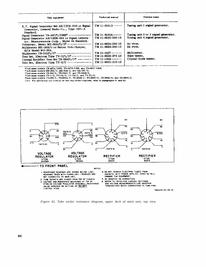
94
Figure 42. Tube socket resistance diagram, upper deck of main unit, top view.
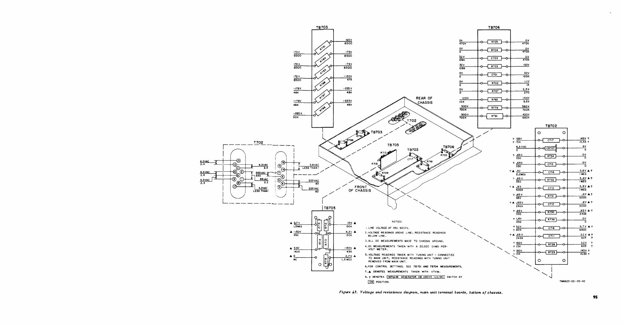
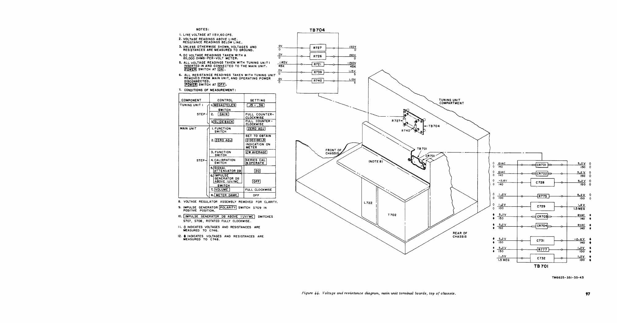
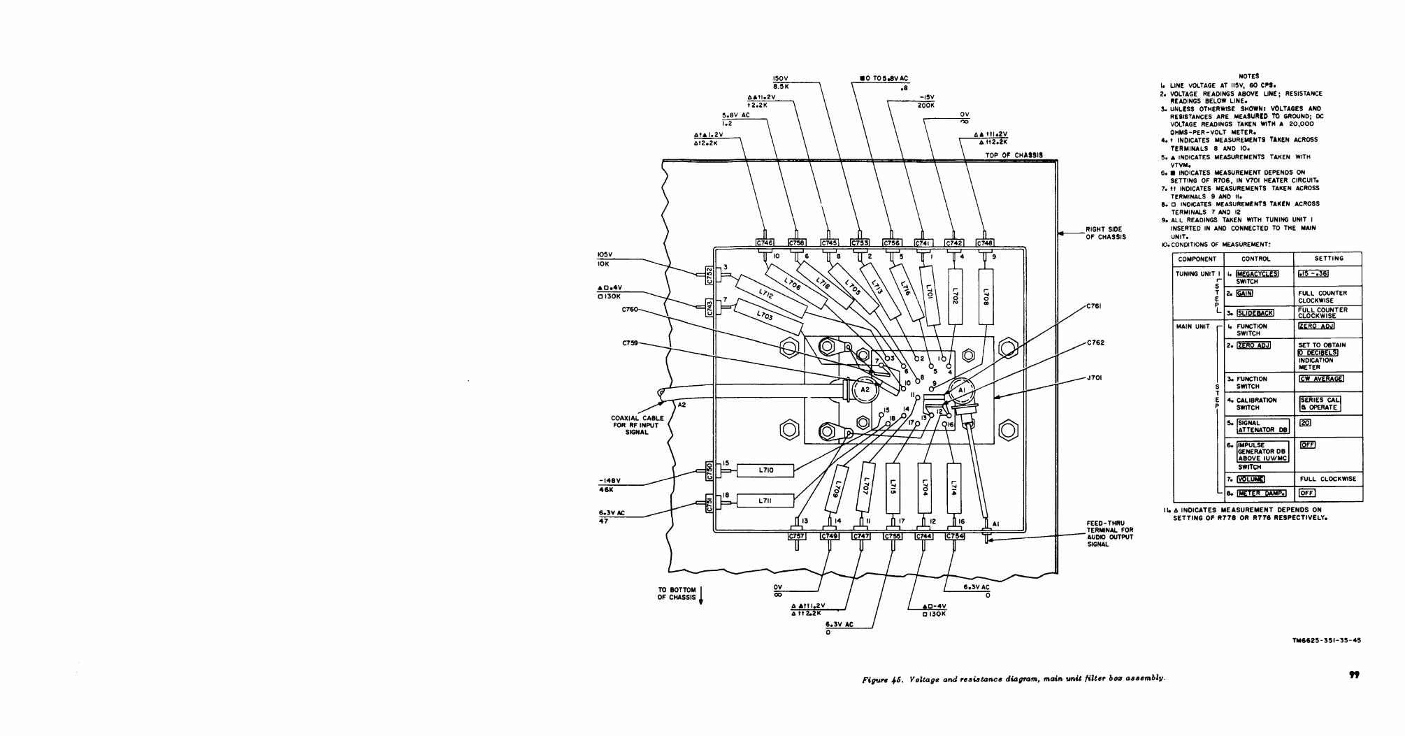
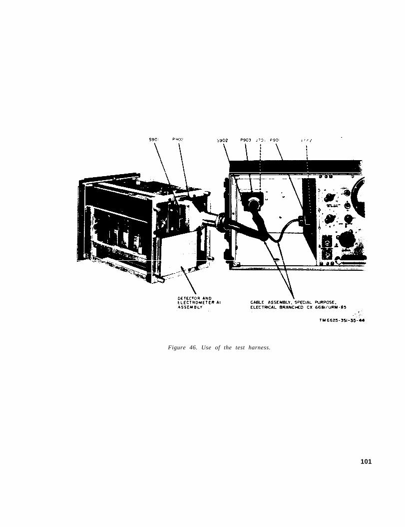
Figure 46. Use of the test harness.
101
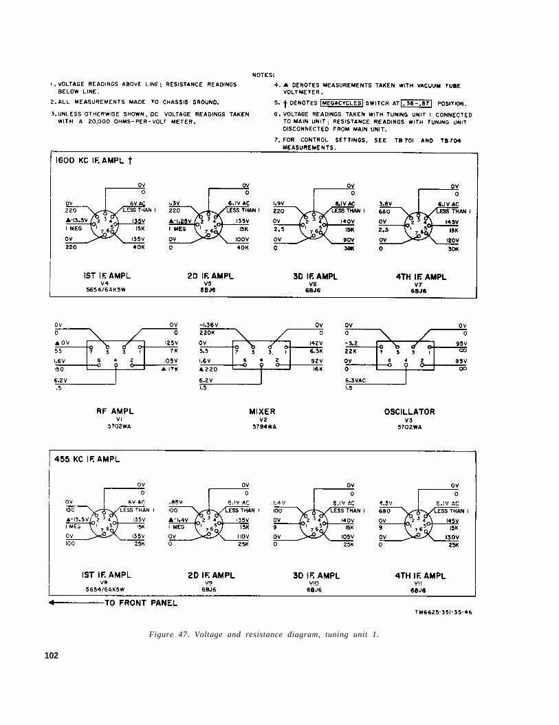
Figure 47. Voltage and resistance diagram, tuning unit 1.
102
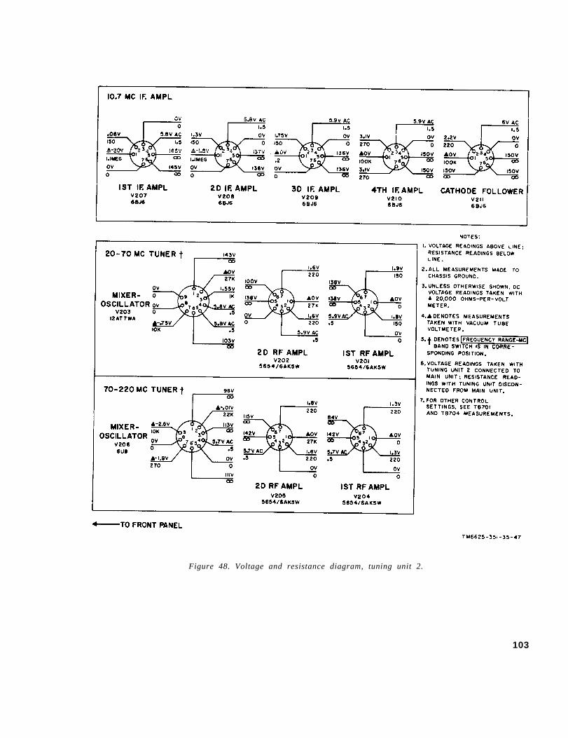
Figure 48. Voltage and resistance diagram, tuning unit 2.
103
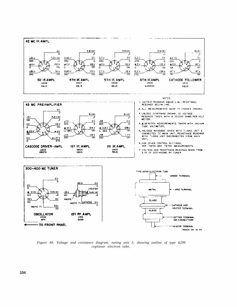
Figure 49. Voltage and resistance diagram, tuning unit 3, showing outline of type 6299coplanar electron tube,
104
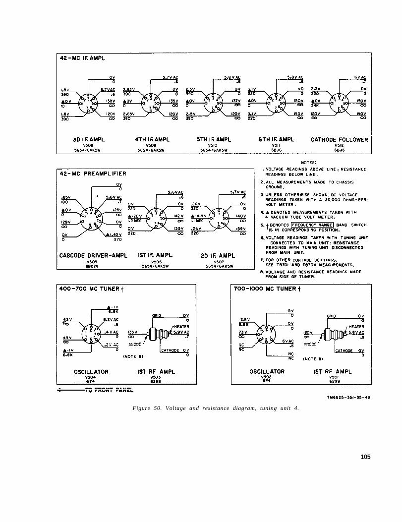
Figure 50. Voltage and resistance diagram, tuning unit 4.
105
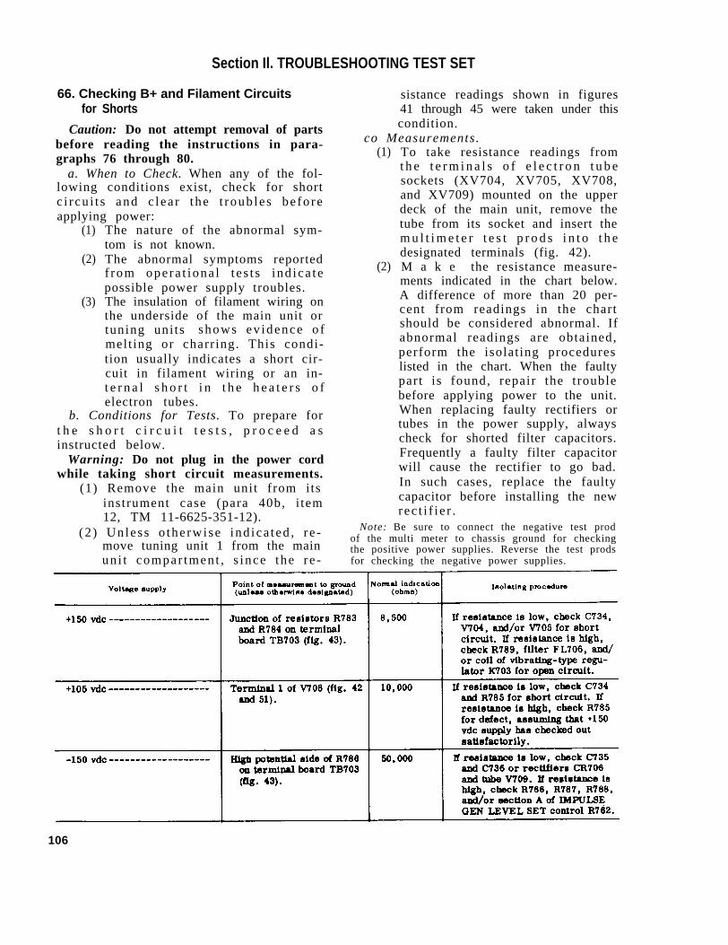
Figure 43.
Figure 42.
Figure 51.
Figure 43.
Section Il. TROUBLESHOOTING TEST SET
66. Checking B+ and Filament Circuitsfor Shorts
Caution: Do not attempt removal of partsbefore reading the instructions in para-graphs 76 through 80.
a. When to Check. When any of the fol-lowing conditions exist, check for shortc i r cu i t s and c l ea r the t roub les be fo reapplying power:
(1)
(2)
(3)
The nature of the abnormal sym-tom is not known.The abnormal symptoms reportedf rom opera t iona l t e s t s ind ica tepossible power supply troubles.The insulation of filament wiring onthe underside of the main unit ortuning uni ts shows ev idence o fmelt ing or charring. This condi-tion usually indicates a short cir-cuit in filament wiring or an in-t e r n a l s h o r t i n t h e h e a t e r s o felectron tubes.
b. Conditions for Tests. To prepare fort h e s h o r t c i r c u i t t e s t s , p r o c e e d a sinstructed below.
Warning: Do not plug in the power cordwhile taking short circuit measurements.
(1) Remove the main unit from itsinstrument case (para 40b, i tem12, TM 11-6625-351-12).
(2 ) Unless o the rwise ind ica ted , r e -move tuning unit 1 from the mainun i t compar tmen t , s ince the r e -
sistance readings shown in figures41 through 45 were taken under thiscondition.
co Measurements.(1)
(2)
To take resistance readings fromt h e t e r m i n a l s o f e l e c t r o n t u b esockets (XV704, XV705, XV708,and XV709) mounted on the upperdeck of the main unit, remove thetube from its socket and insert them u l t i m e t e r t e s t p r o d s i n t o t h edesignated terminals (fig. 42).M a k e the resistance measure-ments indicated in the chart below.A difference of more than 20 per-cent from readings in the chartshould be considered abnormal. Ifabnormal readings are obtained,perform the isolat ing procedureslisted in the chart. When the faultypart is found, repair the troublebefore applying power to the unit.When replacing faulty rectifiers ortubes in the power supply, alwayscheck for shorted filter capacitors.Frequently a faulty filter capacitorwill cause the rectifier to go bad.In such cases, replace the faultycapacitor before installing the newrec t i f i e r .
Note: Be sure to connect the negative test prodof the multi meter to chassis ground for checkingthe positive power supplies. Reverse the test prodsfor checking the negative power supplies.
106
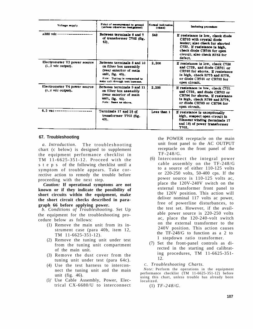
Figure 45.
Figure 45.
Figure 43.
Figure 49.
67. Troubleshooting
a. Introduction. T h e t r o u b l e s h o o t i n gchart (c below) is designed to supplementthe equipment performance checklist inTM 11-6625-351-12 . P roceed wi th thes t e p s of the following checklist until asymptom of trouble appears. Take cor-rective action to remedy the trouble beforeproceeding with the next step.
Caution: If operational symptoms are notknown or if they indicate the possibility ofshort circuits within the equipment, makethe short circuit checks described in para-graph 66 before applying power.
b. Conditions of Troubleshooting. Set Upthe equipment for the troubleshooting pro-cedure below as follows:
(1)
(2)
(3)
(4)
(5)’
Remove the main unit from its in-strument case (para 40b, item 12,TM 11-6625-351-12).Remove the tuning unit under testfrom the tuning unit compartmentof the main unit.Remove the dust cover from thetuning unit under test (para 64c).Use the test harness to intercon-nect the tuning unit and the mainunit (fig. 46).Use Cable Assembly, Power, Elec-tr ical CX-6680/U to interconnect
(6)
(7)
the POWER receptacle on the mainunit front panel to the AC OUTPUTreceptacle on the front panel of theTF-248/G.In te rconnec t the in teg ra l powercable assembly on the TF-248/Gto a source of either 110-125 voltsor 220-250 volts, 50-400 cps. If thepower source is 110-125 volts ac,place the 120V-240V switch on theexternal transformer front panel tothe 120V position. This action willdeliver nominal 117 volts ac power,free of powerline disturbances, tothe test set. However, if the avail-able power source is 220-250 voltsac, place the 120-240-volt switchon the external transformer to the240V position. This action causesthe TF-248/G to function as a 2 to1 stepdown ratio transformer.Set the front-panel controls as di-rected in the starting and calibrat-ing procedures, TM 11-6625-351-12.
C . Troubleshooting Charts.Note: Perform the operations in the equipment
performance checklist (TM 11-6625-351-12) beforeusing this chart, unless trouble has already beenlocal ized.
(1) TF-248/G.
107
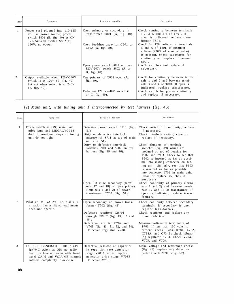
S t e p
1
2
Step
1
2
3
Symptom
Power cord plugged into 110-125-volt ac power source; powerswitch S801 (B, fig. 40) at ON.120-240-volt switch S802 at120V; no output.
Output available when 120V-240Vswitch is at 120V (B, fig. 40)but not when switch is at 240V(c, fig. 40).
108
Probab le t roub le
Open primary or secondary intransformer T801 (A, fig. 40).
Open feedthru capacitor C801 orC802 (A, fig. 40).
Open power switch S801 or open120V-240V switch S802 (A orB, fig. 40).
One primary of T801 open (A,fig. 40).
Defective 120 V-240V switch (Bor C, fig. 40).
Correc t ion
Check continuity between terminals1-2, 3-4, and 5-6 of T801. Ifopen is indicated, replace trans-former T801.
Check for 120 volts ac at terminals5 and 6 of T801. If incorrectvoltage (+20% of nominal value)is present , check capacitors forcontinuity and replace if neces-sary .
Check switches and replace ifn e c e s s a r y .
Check for continuity between termi-nals 1 and 2 and between termi-nals 3 and 4 of T801. If open isindicated, replace transformer.
Check switch for proper continuityand replace if necessary.
(2) Main unit, with tuning unit 1 interconnected by test harness (fig. 46).
Symptom
Power switch at ON; main unitpilot lamp and MEGACYCLESdial illumination lamps on tuningunit do not light.
Pilot ad MEGACYCLES dial i l lu-mination lamps light; equipmentdoes not operate.
INPULSE GENERATOR DB ABOVElµV/MC switch at ON; no audioheard in headset, even with frontpanel GAIN and VOLUME controlsrotated completely clockwise.
Probab le t roub le
Defective power switch S710 (fig.51).
Dirty or defective interlockmicroswitch S711 at top of mainunit (fig. 51).
Dirty or defective interlockswitches S901 and S902 on testharness (fig. 39 and 46).
Open 6.3 v ac secondary (termi-nals 17 and 18) or open primary(terminals 1 and 2) of powertransformer T702 (fig. 51).
Open secondary on power trans-former T702 (fig. 43).
Defective rectifiers CR701through CR707 (fig. 43, 52 and55) .
Defective rectif ier V704 andV705 (fig. 43, 51, 52, and 54).Defective regulator V708.
Defective resistor or capacitorin repeti t ion rate generatorstage V703A or in impulsegenerator drive stage V703B.Defective V703.
Correc t ion
Check switch for continuity; replaceif necessary.
Check interlock switch; clean orreplace if necessary.
Check plungers of interlockswitches (fig. 39) which aremounted on top of housing forP902 and P903. Check to see thatP902 is inserted as far as possi-ble into mating connector on tun-ing unit; similarly, see that P903is inserted as far as possibleinto connector J701 in main unit.Clean or replace switches ifn e c e s s a r y .
Check continuity of primary (termi-nals 1 and 2) and between termi-nals 17 and 18 of transformer. Ifopen is indicated, replace trans-f o r m e r .
Check continuity between secondaryterminals. If secondary is open,r e p l a c e t r a n s f o r m e r .
Check rectifiers and replace anyfound defective.
Measure voltage at terminal 2 ofP701. If less than 150 volts ispresent, check R783, R784, L722,C734A, and C734B; check vibrat-ing regulator K703. Check V704,V705, and V708.
Make voltage and resistance checks(fig. 41); replace any defectiveparts. Check V703 (fig. 52).
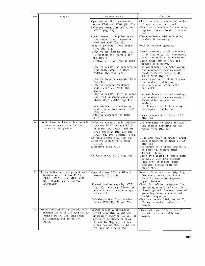
Step
4
5
Symptom
Audio heard in headset, but no indication on meter with functionswitch at any position.
Meter indications are present withfunction switch at CW PEAK,PULSE PEAK, and METEREDSLIDEBACK, but not at CWAVERAGE.
6 Meter indications are present withfunction switch at CW AVERAGE,PULSE PEAK, and METEREDSLIDEBACK, but not at CWPEAK.
Probab le t roub le
Open coil or dirty contacts ofrelays K701 and K702 (fig. 52).
Defective attenuators AT701 orAT702 (fig. 52).
Open resistor in impulse gener-ator output control networksS707 and S708 (fig. 53).
Impulse generator G701 inoper-ative (fig. 51).
Defective test harness (fig. 39).(Disconnect test harness forthis test. )
Defective VOLUME control R701
Defective resistor or capacitor infirst audio amplifier stageV701A. Defective V701.
Defective coupling capacitor C703(fig. 43).
Defective voltage regulatorsV706, V707, and V709 (fig. 51and 52) .
Defective resistor R707 or capac-itor C704 in second audio am-plifier stage V701B (fig. 41).
Open primary or secondary of audio output transformer T701(fig. 52).
Defective component in filterFL701.
Defective meter cathode followerresistors R712 through R719,or meter multiplier resistorsR723 and R724 (fig. 53), andR725 (fig. 10). Defective V702.
Defective switch S702 (fig. 53) --Defective component in filter
FL702.D e f e c t i v e j a c k J 7 0 4 - - - - - - - - - - - -
Defective meter M701 (fig. 53) --
Open rf choke L711 in fiIter boxassembly (fig. 45).
Shorted feedthru capacitpr C751(fig. 8), grounding 6.3-volt acpower to electrometer relaysK1 and K2.
Defective section Z of functionswitch S702 (fig. 52 and 53).
Shorted section Z of functionswitch S702 (fig. 52 and 53),improperly applying 6.3-volt acpower to electrometer relaysK1 and K2 (fig. 59). (In thisswitch position (fig. 8), K1 andK2 must be deenergized.)
Correc t ion
Check coils with ohmmeter; replaceif open or short circuited.
Check with ohmmeter for continuity;replace if open circuit is indica-ted.
Check resistors with ohmmeter;replace if necessary.
Replace impulse generator.
Check continuity of all conductorsin test harness, with ohmmeter;repair or replace, i f necessary.
Check potentiometer R701 andreplace if defective.
Use voltohmmeter to make voltageand resistance measurements tolocate defective part (fig. 41).Check V701 (fig. 52).
Check capacitor for short or openand replace if defective.
Check regulators V706, V707,and V709.
Use voltohmmeter to make voltageand resistance measurements tolocate defective part, andreplace.
Use ohmmeter to check windings,and replace if defective.
Check components in filter FL701(fig. 55).
Use ohmmeter to check resistors,and replace defective resistor .Check V702 (fig. 52).
Clean and repair or replace switch.Check components in filter FL702
(fig. 55).Use ohmmeter to check continuity.
If defective, replace filterFL702 (fig. 55).
Check by plugging in remote meterto RECORDER EXT METERjack J704. if remote meteroperates, replace main unitmeter M701.
Remove filter box cover (fig. 51),disconnect power, and checkL711 for continuity. Replace ifopen circuited.
Check for infinite resistance fromprotruding terminal of C751 tochassis ground. Remove cause ofgrounding center conductor offeedthru capacitor.
Clean and repair S702, section Z,(front) or replace defectiveswitch.
Clean and repair S702 section Z(front), or replace defectiveswitch.
109
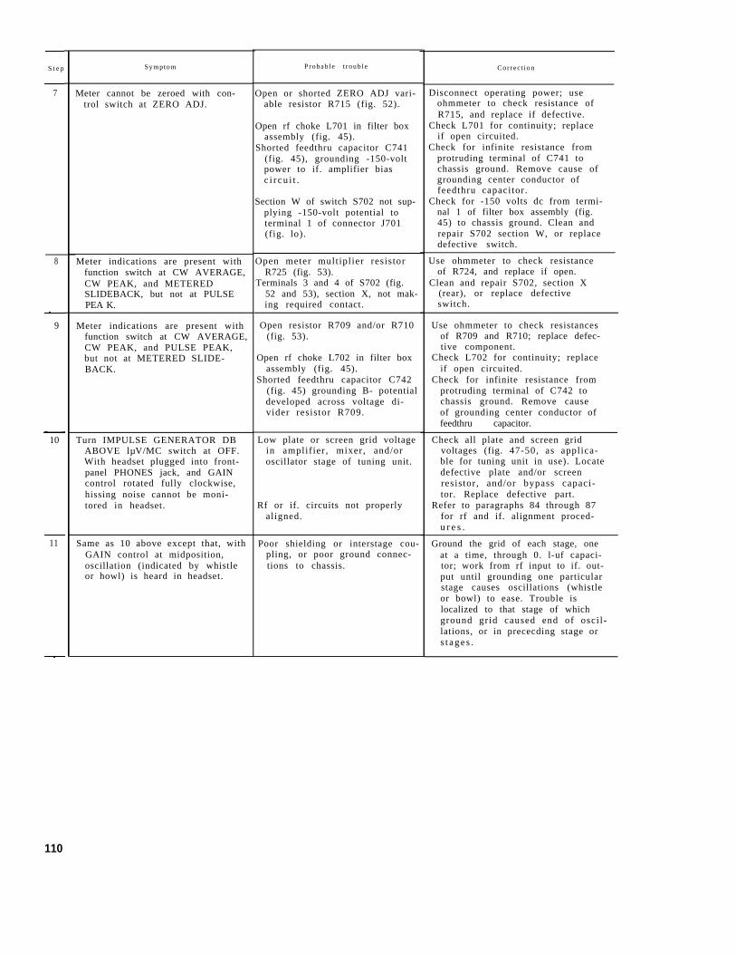
S t e p
7
8
9
10
11
110
Symptom
Meter cannot be zeroed with con-trol switch at ZERO ADJ.
Meter indications are present withfunction switch at CW AVERAGE,CW PEAK, and METEREDSLIDEBACK, but not at PULSEPEA K.
Meter indications are present withfunction switch at CW AVERAGE,CW PEAK, and PULSE PEAK,but not at METERED SLIDE-BACK.
Turn IMPULSE GENERATOR DBABOVE lµV/MC switch at OFF.With headset plugged into front-panel PHONES jack, and GAINcontrol rotated fully clockwise,hissing noise cannot be moni-tored in headset.
Same as 10 above except that, withGAIN control at midposition,oscillation (indicated by whistleor howl) is heard in headset.
Probab le t roub le
Open or shorted ZERO ADJ vari-able resistor R715 (fig. 52).
Open rf choke L701 in filter boxassembly (fig. 45).
Shorted feedthru capacitor C741(fig. 45), grounding -150-voltpower to if. amplifier biasc i r cu i t .
Section W of switch S702 not sup-plying -150-volt potential toterminal 1 of connector J701(fig. lo).
Open meter multiplier resistorR725 (fig. 53).
Terminals 3 and 4 of S702 (fig.52 and 53), section X, not mak-ing required contact.
Open resistor R709 and/or R710(fig. 53).
Open rf choke L702 in filter boxassembly (fig. 45).
Shorted feedthru capacitor C742(fig. 45) grounding B- potentialdeveloped across voltage di-vider resistor R709.
Low plate or screen grid voltagein amplifier , mixer, and/oroscillator stage of tuning unit.
Rf or if. circuits not properlyaligned.
Poor shielding or interstage cou-pling, or poor ground connec-tions to chassis.
Correc t ion
Disconnect operating power; useohmmeter to check resistance ofR715, and replace if defective.
Check L701 for continuity; replaceif open circuited.
Check for infinite resistance fromprotruding terminal of C741 tochassis ground. Remove cause ofgrounding center conductor offeedthru capacitor.
Check for -150 volts dc from termi-nal 1 of filter box assembly (fig.45) to chassis ground. Clean andrepair S702 section W, or replacedefective switch.
Use ohmmeter to check resistanceof R724, and replace if open.
Clean and repair S702, section X(rear), or replace defectiveswitch.
Use ohmmeter to check resistancesof R709 and R710; replace defec-tive component.
Check L702 for continuity; replaceif open circuited.
Check for infinite resistance fromprotruding terminal of C742 tochassis ground. Remove causeof grounding center conductor offeedthru capacitor.
Check all plate and screen gridvoltages (fig. 47-50, as applica-ble for tuning unit in use). Locatedefective plate and/or screenresistor , and/or bypass capaci-tor. Replace defective part.
Refer to paragraphs 84 through 87for rf and if. alignment proced-u r e s .
Ground the grid of each stage, oneat a time, through 0. l-uf capaci-tor; work from rf input to if. out-put until grounding one particularstage causes oscillations (whistleor bowl) to ease. Trouble islocalized to that stage of whichground grid caused end of osci l-lations, or in prececding stage ors t a g e s .
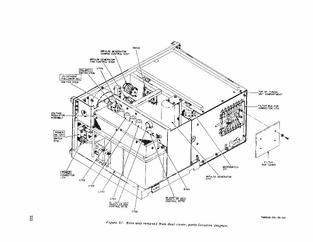
Figure 51.
111

This page left blank intentionally.
112
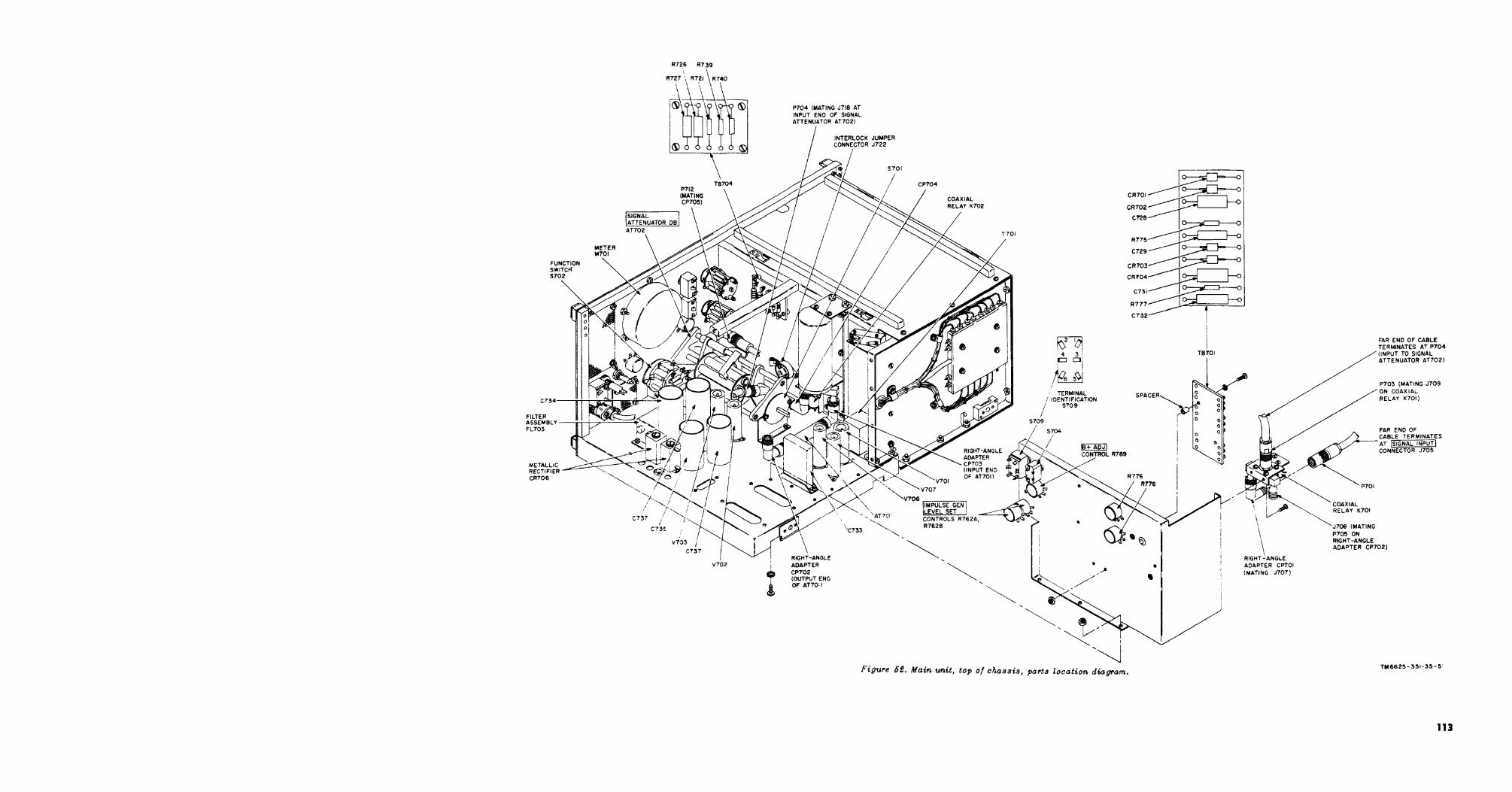
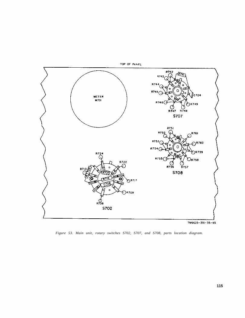
Figure 53. Main unit, rotary switches S702, S707, and S708, parts location diagram.
115
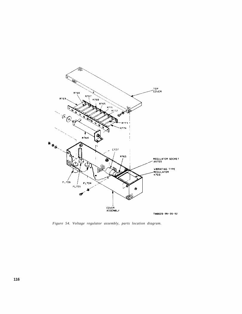
Figure 54. Voltage regulator assembly, parts location diagram.
116
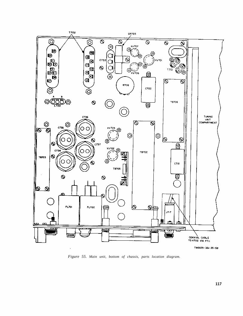
Figure 55. Main unit, bottom of chassis, parts location diagram.
117
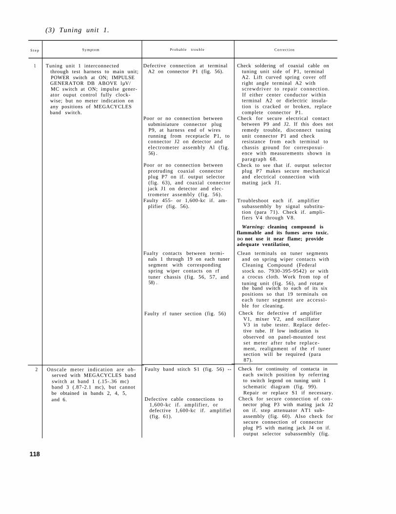
(3) Tuning unit 1.
S t e p
1
2
Symptom
Tuning unit 1 interconnectedthrough test harness to main unit;POWER switch at ON; IMPULSEGENERATOR DB ABOVE lµV/MC switch at ON; impulse gener-ator ouput control fully clock-wise; but no meter indication onany positions of MEGACYCLESband switch.
Onscale meter indicat ion are ob-served with MEGACYCLES bandswitch at band 1 (.15-.36 mc)band 3 (.87-2.1 mc), but cannotbe obtained in bands 2, 4, 5,and 6.
Probab le t roub le
Defective connection at terminalA2 on connector P1 (fig. 56).
Poor or no connection betweensubminiature connector plugP9, at harness end of wiresrunning from receptacle P1, toconnector J2 on detector andelectrometer assembly Al (f ig.56) .
Poor or no connection betweenprotruding coaxial connectorplug P7 on if. output selector(fig. 63), and coaxial connectorjack J1 on detector and elec-trometer assembly (fig. 56).
Faulty 455- or 1,600-kc if. am-plifier (fig. 56).
Fualty contacts between termi-nals 1 through 19 on each tunersegment with correspondingspring wiper contacts on rftuner chassis (fig. 56, 57, and58) .
Faulty rf tuner section (fig. 56)
Faulty band stitch S1 (fig. 56) --
Defective cable connections to1,600-kc if . amplifier , ordefective 1,600-kc if. amplifiel(fig. 61).
Correc t ion
Check soldering of coaxial cable ontuning unit side of P1, terminalA2. Lift curved spring cover offright angle terminal A2 withscrewdriver to repair connection.If either center conductor withinterminal A2 or dielectric insula-tion is cracked or broken, replacecomplete connector P1.
Check for secure electrical contactbetween P9 and J2. If this does notremedy trouble, disconnect tuningunit connector P1 and checkresistance from each terminal tochassis ground for correspoxui-ence with measurements shown inparagraph 68.
Check to see that if. output selectorplug P7 makes secure mechanicaland electrical connection withmating jack J1.
Troubleshoot each if. amplifiersubassembly by signal substitu-tion (para 71). Check if. ampli-fiers V4 through V8.
Warning: cleaninq compound isflammable and its fumes areo toxic.DO not use it near flame; provideadequate ventilation e
Clean terminals on tuner segmentsand on spring wiper contacts withCleaning Compound (Federalstock no. 7930-395-9542) or witha crocus cloth. Work from top oftuning unit (fig. 56), and rotatethe band switch to each of its sixpositions so that 19 terminals oneach tuner segment are accessi-ble for cleaning.
Check for defective rf amplifierV1, mixer V2, and oscillatorV3 in tube tester. Replace defec-tive tube. If low indication isobserved on panel-mounted testset meter after tube replace-ment, realignment of the rf tunersection will be required (para87).
Check for continuity of contacta ineach switch position by referringto switch legend on tuning unit 1schematic diagram (fig. 99).Repair or replace S1 if necessary.
Check for secure connection of con-nector plug P3 with mating jack J2on if. step attenuator AT1 sub-assembly (fig. 60). Also check forsecure connection of connectorplug P5 with mating jack J4 on if.output selector subassembly (fig.
118
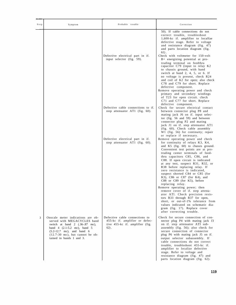
S t e p
3
Symptom
Onscale meter indications are ob-served with MEGACYCLES bandswitch at band 2 (.36-.87 mc),band 4 (2.1-5.2 mc), band 5(5.2-12.7 mc), and band 6(12.7-30 mc), but cannot be ob-tained in bands 1 and 3.
Probab le t roub le Cor rec t ion
Defective electrical part in if.input selector (fig. 59).
Defective cable connections to if.step attenuator AT1 (fig. 60).
Defective electrical part in if.step attenuator AT1 (fig. 60).
Defective cable connections to455-kc if. amplifier or defec-tive 455-kc if. amplifier (fig.62) .
50). If cable connections do notcorrect t rouble, t roubleshoot1,600-kc if. amplifier to localfaedefective stage. Refer to voltageand resistance diagram (fig. 47)and parts location diagram (fig.61) .
Check with voltmeter for 150-voltB+ energizing potential at pro-truding terminal on feedthrucapacitor C79 (input to relay K2to chassis ground, with bandswitch at band 2, 4, 5, or 6. Ifno voltage is present, check R24and coil of K2 for open; also checkC78 and C79 for short. Replacedefective component.
Remove operating power and checkprimary and secondary windingsof T23 for open circuit. checkC71 and C77 for short. Replacedefective component.
Check for secure electrical contactbetween connector plug P8 andmating jack J6 on if. input selec-tor (fig. 56 and 59) and betweenconnector plug P2 and matingjack J1 on if. step attenuator AT1(fig. 60). Check cable assemblyW1 (fig. 56) for continuity; repairor replace if necessary.
Remove operating power and checkfor continuity of relays K3, K4,and K5 (fig. 60) to chassis ground.Convenient test points are at pro-truding center terminals of feed-thru capacitors C85, C86, andC88. If open circuit is indicatedat any test, suspect R31, R32, orR38 before replacing relay. Ifzero resistance is indicated,suspect shorted C84 or C85 (forK3), C86 or C87 (for K4), andC88 or C89 (for K5), beforereplacing relay.
Remove operating power; thenremove cover of if. step attenu-ator ATl. Check precision resis-tors R33 through R37 for open,short, or out-of-1% tolerance fromvalues indicated on schematic dia-gram (fig. 17). Replace coverafter correcting trouble.
Check for secure connection of con-nector plug P4 with mating jack J3on if. step attenuator ATI sub-assembly (fig. 56); also check forsecure connection of connectorplug P6 with mating jack J5 on if.output selector subassembly. Ifcable connections do not correcttrouble, troubleshoot 455-kc if.amplifier to localize defectivestage. Refer to voltage andresistance diagram (fig. 47) andparts location diagram (fig. 62).
119
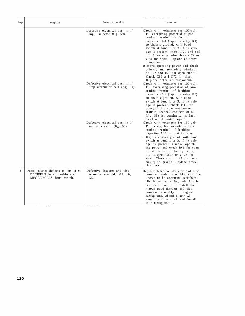
Step
4
Symptnm
Meter pointer deflects to left of 0DECIBELS in all positions ofMEGACYCLES band switch.
Probab le t roub le
Defective electrical part in if.input selector (fig. 59).
Defective electrical part in if.step attenuator ATl (fig. 60).
Defective electrical part in if.output selector (fig. 63).
Defective detector and elec-trometer assembly A1 (fig.56).
Correc t ion
Check with voltmeter for 150-voltB+ energizing potential at pro-truding terminal on feedthrucapacitor C74 (input to relay K1)to chassis ground, with bandswitch at band 1 or 3. If no volt-age is present, check R21 and coilof K1 for open; also check C73 andC74 for short. Replace defectivecomponent.
Remove operating power and checkprimary and secondary windingsof T22 and R22 for open circuit.Check C69 and C72 for short.Replace defective component.
Check with voltmeter for 150-voltB+ energizing potential at pro-truding terminal of feedthrucapacitor C88 (input to relay K5)to chassis ground, with bandswitch at band 1 or 3. If no volt-age is present, check R38 foropen; if this does not correcttrouble, recheck contacts of S1(fig. 56) for continuity, as indi-cated in S1 switch legend.
Check with voltmeter for 150-voltB + energizing potential at pro-truding terminal of feedthrucapacitor C128 (input to relayK6) to chassis ground, with bandswitch at band 1 or 3. If no volt-age is present, remove operat-ing power and check R61 for opencircuit before replacing relay;also suspect C127 or C128 forshort. Check coil of K6 for con-tinuity to ground. Replace defec-tive part.
Replace defective detector and elec-trometer sealed assembly with oneknown to be operating satisfacto-rily in another tuning unit. If thisremedies trouble, reinstal l theknown good detector and elec-trometer assembly in originaltuning unit. Obtain a new Alassembly from stock and installit in tuning unit 1.
120
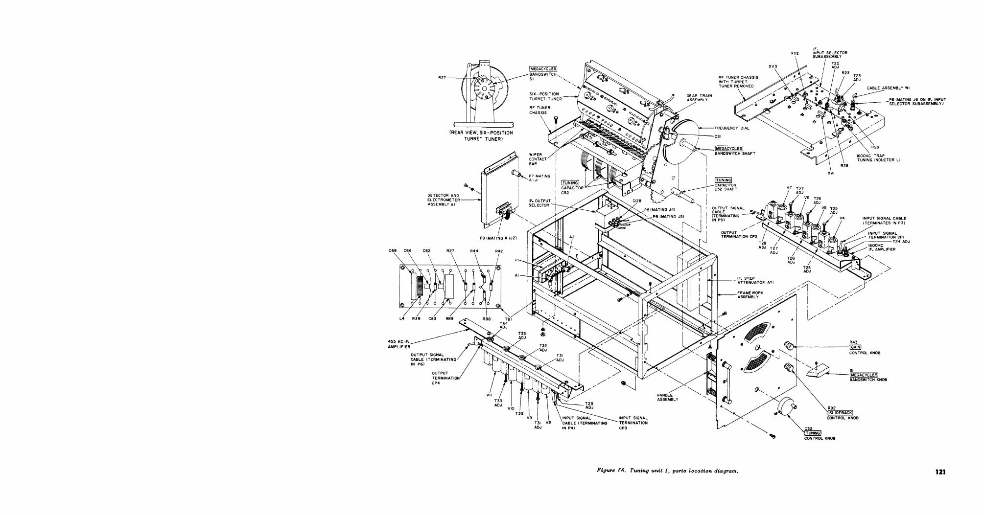
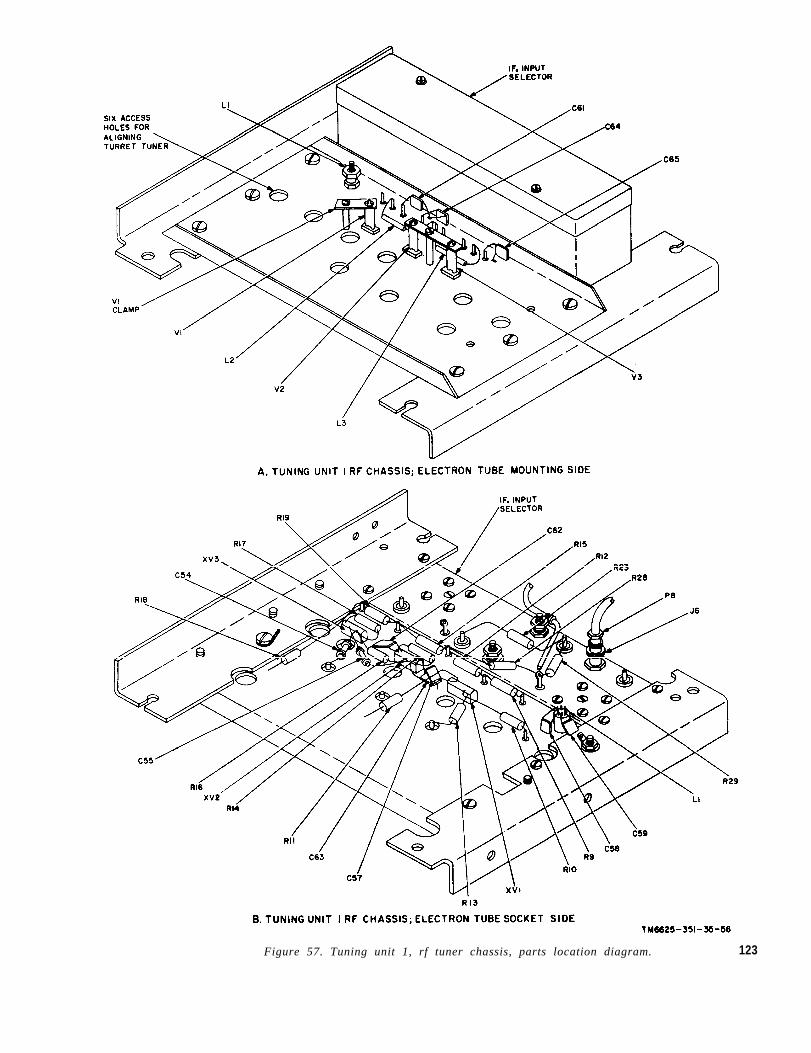
Figure 57. Tuning unit 1, rf tuner chassis, parts location diagram. 123
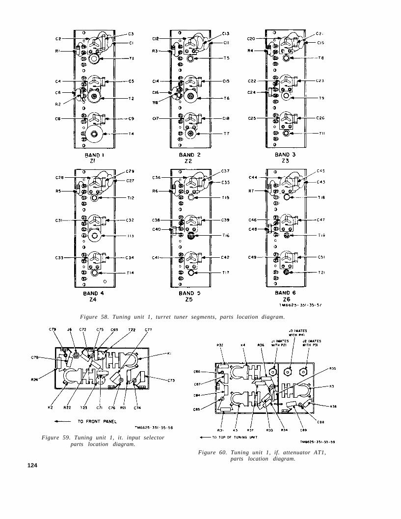
Figure 58. Tuning unit 1, turret tuner segments, parts location diagram.
Figure 59. Tuning unit 1, it. input selectorparts location diagram.
Figure 60. Tuning unit 1, if. attenuator AT1,parts location diagram.
124
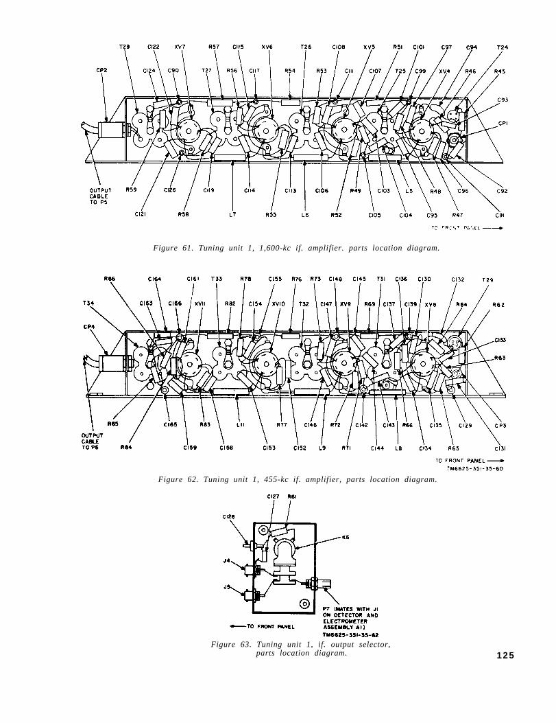
Figure 61. Tuning unit 1, 1,600-kc if. amplifier. parts location diagram.
Figure 62. Tuning unit 1, 455-kc if. amplifier, parts location diagram.
Figure 63. Tuning unit 1, if. output selector,parts location diagram. 125
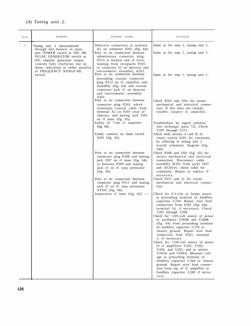
(4) Tuning unit 2.
S t e p
1
126
Symptom
Tuning unit 2 interconnectedthrough test harness to mainunit; POWER switch at ON; IM-PULSE GENERATOR switch atON; impulse generator outputcontrols fully clochwise; but nometer indication at either positionof FREQUENCY RANGE-MCswitch.
Probab le t roub le
Defective connection at terminalA2 on connector P201 (fig. 64).
Poor or no connection betweensubminiature connector plugP213 at harness end of wiresrunning from receptacle P201to connector J2 on detector andelectrometer assembly A201.
Poor or no connection betweenprotruding coaxial connectorplug P212 on if. amplifier sub-assembly (fig. 64) and coaxialconnector jack J1 on detectorand electrometer assemblyA201.
Poor or no connection betweenconnector plug P202, whichterminates coaxial cable fromterminal A2 on P201 (rear ofchassis), and mating jack J201on rf tuner (fig. 65).
Faulty 10. 7-mc if. amplifier(fig. 64) .
Faulty contacts on band switchS201 (fig. 65).
Poor or no connection betweenconnector plug P208 and matingjack J207 on rf tuner (fig. 64),or between P209 and matingjack J1 on if. step attenuator(fig. 66).
Poor or no connection betweenconnector plug P211 and matingjack J2 on if. step attenuatorAT201 (fig. 66).
Inoperative rf tuner (fig. 65) ----
Correc t ion
Same as for step 1, tuning unit 1.
Same as for step 1, tuning unit 1.
Same as for step 1, tuning unit 1.
Check P202 and J201 for securemechanical and electrical connec-tion. If this does not remedytrouble, suspect if . amplifier .
Troubleshoot by signal substitu-tion technique (para 72). CheckV207 through V211.
Check both section A and B ofrotary switch S201 for continuityby referring to tuning unit 2overall schematic diagram (fig.100).
Check P208 and J201 (fig. 65) forsecure mechanical and electr icalconnection. Disconnect cableassembly W201 from jacks J207and AT201J1; check cable forcontinuity. Repair or replace ifn e c e s s a r y .
Check P211 and J2 for securemechanical and electrical connec-tion.
Check for 6.3-volt ac heater powerat protruding terminal of feedthrucapacitor C250. Repair wire leadconnection from P201 (fig. 64),terminal 16, i f necessary. CheckV201 through V206.
Check for +105-volt source of powerto oscillators V203B and V206B(fig. 64) from protruding terminalof feedthru capacitor C270 tochassis ground, Repair wire leadconnection from P201, terminal3, if necessary.
Check for +150-volt source of powerto rf amplifiers V201, V202,V204, and V205, and to mixersV203A and V206A. Measure volt-age at protruding terminal offeedthru capacitor C264 to chassisground. Repair wire lead connec-tion from top of if. amplifier atfeedthru capacitor C280 if neces-s a r y .
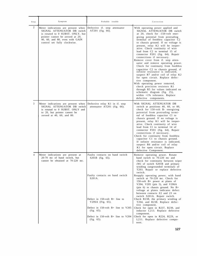
S t e p Symptom Probab le t roub le C o r r e c t i o n
2 Meter indications are present whenSIGNAL ATTENUATOR DB switchis rotated to 0 SUBST. ONLY, butpointer cannot be zeroed at 20,40, 60, and 80, even with GAINcontrol set fully clockwise.
Defective if. step attenuatorAT201 (fig. 66).
With operating power applied andSIGNAL ATTENUATOR DB switchat 20, check for -150-volt ener-gizing potential from protrudingterminal of feedthru capacitor C2to chassis ground. If no voltage ispresent, relay K2 will be inoper-ative. Check continuity of wirelead from C2 to terminal 15 ofconnector P201 (fig. 64). Repairconnections if necessary.
Remove cover from if. step atten-uator and remove operating power.Check for continuity from feedthrucapacitior C2 to chassis ground. rfinfinite resistance is indicated,suspect R7 and/or coil of relay K2for open circuit. Replace defec-tive component.
With operating power removed,check precision resistors R1through R5 for values indicated onschematic diagram (fig. 25),within +1% tolerance. Replacedefective components.
3
4
Meter indications are present whenSIGNAL ATTENUATOR DB switchis rotatad to 0 SUBST. ONLY andto 20, but pointer cannot bezeroed at 40, 60, and 80.I
Meter indications are present at20-70 mc of band switch, butcannot be obtained at 70-220 mc.
Defective relay K1 in if. stepattenuator AT201 (fig. 66).
Faulty contacts on band switchS201B (fig. 65).
Faulty contacts on band switchS201A.
Defect in 150-volt B+ line toV206A (Fig. 65).
Defect in 150-volt B+ line to V205(fig. 65).
Defect in 150-volt B+ line to V204(fig. 65).
With SIGNAL ATTENUATOR DBswitch at positions 40, 60, or 80,check for 150-volt B- energizingpotential from protruding termi-nal of feedthru capacitor Cl tochassis ground. If no voltage ispresent, relay K1 will be inoper-ative. Check continuity of wirelead from Cl to terminal 14 ofconnector P201 (fig. 64). Repairconnections if necessary.
Check for continuity from feedthrucapacitor C1 to chassis ground.If infinite resistance is indicated,suspect R6 and/or coil of relayK1 for open circuit. Replacedefective Component.
Remove operating power. Rotateband switch to 70-220 mc andcheck for continuity between wiper(W) of switch S201B and primarywinding (ungrounded terminal) ofT203. Repair or replace defectiveswitch.
Reapply operating power, with bandswitch at 70-220 mc. Check for150-volt B+ power at plates ofV204, V205 (pin 5), and V206A(pin 6) to chassis ground. No B+voltage at plates indicates defectbetween contacts Z2 and 23 onswitch S201A. Repair switch.
Check R238, the primary winding ofT204, and R238. Replace defec-tive component.
Check for open in R237, R239, andinductor L213. Replace defectivecomponent.
Check for open in R224, R22S, orL211. Replace defective compo-nent.
127
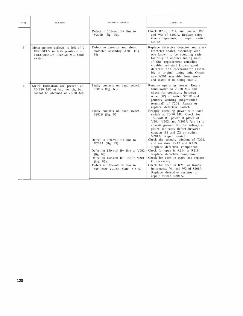
S t e p
5
6
Symptom
Meter pointer deflects to left of 0DECIBELS in both positions ofFREQUENCY RANGE-MC bandswitch.
Meter Indication are present at70-220 MC of bad switch, butcannot be obtained at 20-70 MC.
Probab le t roub le
Defect in 105-volt B+ line toV206B (fig. 65).
Defective detector and elec-trometer assembly A201 (fig.64) .
Faulty contacts on band switchS201B (fig. 65).
Faulty contacts on band switchS201B (fig. 65).
Defect in 150-volt B+ line toV203A (fig. 65).
Defect in 150-volt B+ line to V202(fig. 65) .
Defect in 150-volt B+ line to V201(fig. 65).
Defect in 105-volt B+ line tooscillator V203B plate, pin 6.
Correc t ion
Check R235, L214, and contact W2and W3 of S201A. Replace defec-tive components, or repair switchS201A.
Replace defective detector and elec-trometer sealed assembly withone known to be operating satis-factorily in another tuning unit.If this replacement remediestrouble, reinstall known gooddetector and electrometer assem-bly in original tuning unit. Obtainnew A201 assembly from stockand install it in tuning unit 2.
Remove operating power. Rotateband switch to 20-70 MC andcheck for continuity betweenwiper (W) of switch S201B andprimary winding (ungroundedterminal) of T201. Repair orreplace defective switch.
Reapply operating power with bandswitch at 20-70 MC. Check for150-volt B+ power at plates ofV201, V202, and V203A (pin 1) tochassis ground. No B+ voltage atplates indicates defect betweencontacts Z1 and Z2 on switchS201A. Repair switch.
Check the primary winding of T202,and resistors R217 and R219.Replace defective component.
Check for open in R214 or R218.Replace defective compmnmt.
Check for open in R209 and replaceif necessary.
Check for open in R216 or troublein contactsa W1 and W2 of S201A.Replace defective resistor orrepair switch S201A.
128
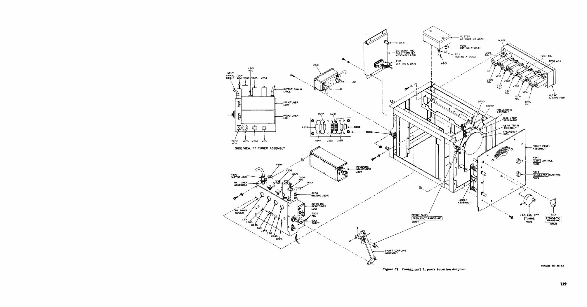
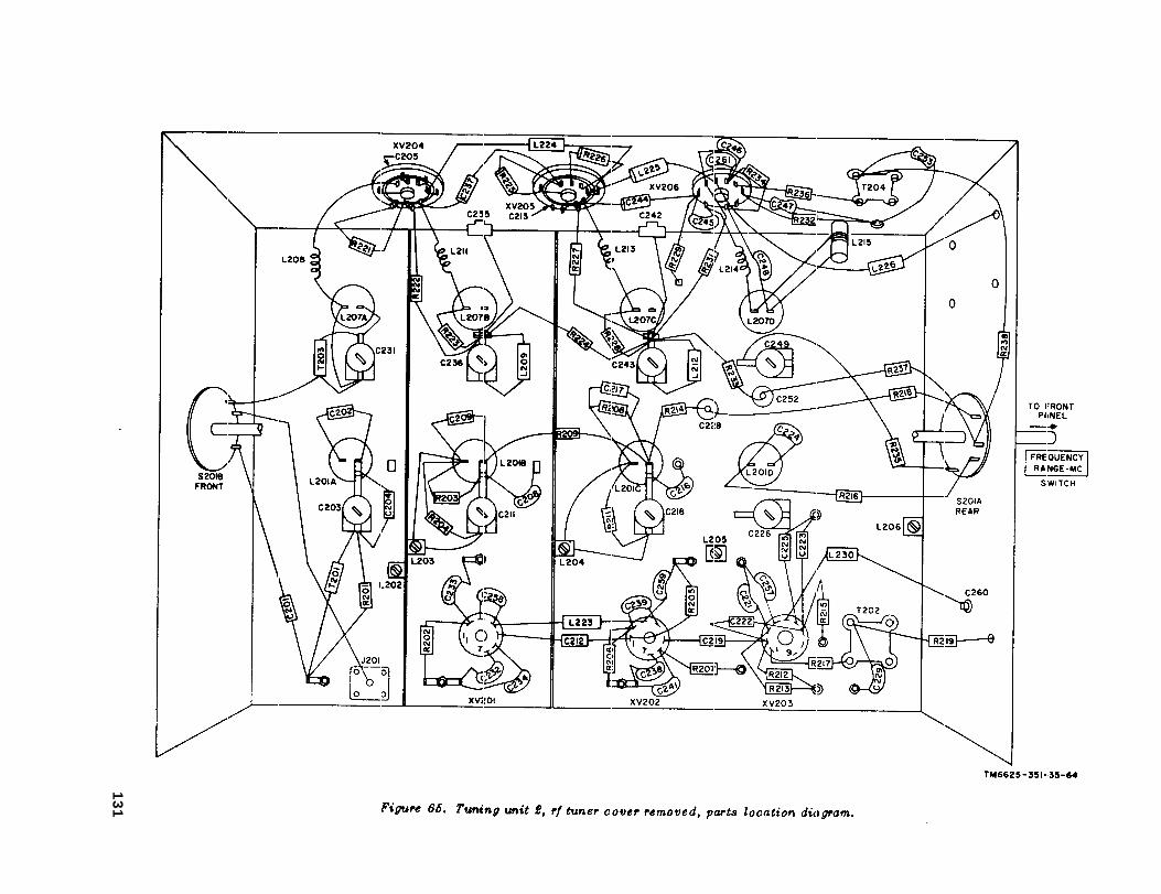
Figure 65.
13
1
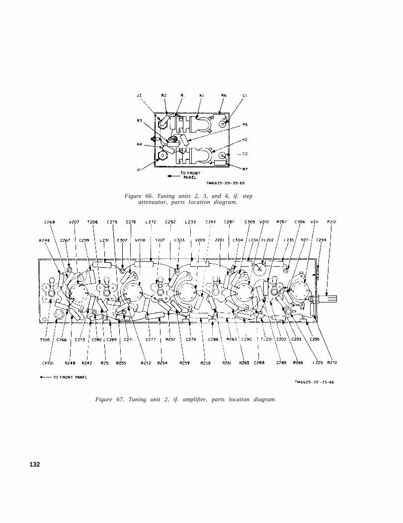
Figure 66. Tuning units 2, 3, and 4, if. stepattenuator, parts location diagram.
Figure 67. Tuning unit 2, if. amplifier, parts location diagram.
132
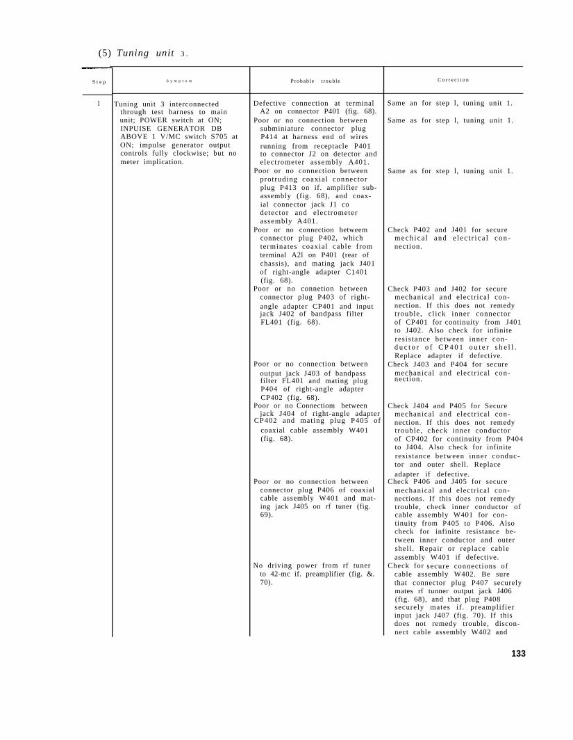
(5) Tuning unit 3 .
S t e p S y m p t o m
1 Tuning unit 3 interconnectedthrough test harness to mainunit; POWER switch at ON;INPUISE GENERATOR DBABOVE 1 V/MC switch S705 atON; impulse generator outputcontrols fully clockwise; but nometer implication.
Probab le t roub le
Defective connection at terminalA2 on connector P401 (fig. 68).
Poor or no connection betweensubminiature connector plugP414 at harness end of wiresrunning from receptacle P401to connector J2 on detector andelectrometer assembly A401.
Poor or no connection betweenprotruding coaxial connectorplug P413 on if. amplifier sub-assembly (fig. 68), and coax-ial connector jack J1 codetector and electrometerassembly A401.
Poor or no connection betweemconnector plug P402, whichterminates coaxial cable fromterminal A2l on P401 (rear ofchassis), and mating jack J401of right-angle adapter C1401(fig. 68).
Poor or no connetion betweenconnector plug P403 of right-angle adapter CP401 and inputjack J402 of bandpass filterFL401 (fig. 68).
Poor or no connection betweenoutput jack J403 of bandpassfilter FL401 and mating plugP404 of right-angle adapterCP402 (fig. 68).
Poor or no Connectiom betweenjack J404 of right-angle adapter
coaxial cable assembly W401(fig. 68).
nection.
CP402 and mating plug P405 of
Poor or no connection betweenconnector plug P406 of coaxialcable assembly W401 and mat-ing jack J405 on rf tuner (fig.69).
No driving power from rf tunerto 42-mc if. preamplifier (fig. &.70).
C o r r e c t i o n
Same an for step l, tuning unit 1.
Same as for step l, tuning unit 1.
Same as for step l, tuning unit 1.
Check P402 and J401 for securem e c h i c a l a n d e l e c t r i c a l c o n -nection.
Check P403 and J402 for securemechanical and electr ical con-nection. If this does not remedytrouble, cl ick inner connectorof CP401 for continuity from J401to J402. Also check for infiniteresistance between inner con-d u c t o r o f C P 4 0 1 o u t e r s h e l l .Replace adapter if defective.
Check J403 and P404 for securemechanical and electr ical con-
Check J404 and P405 for Securemechanical and electr ical con-nection. If this does not remedytrouble, check inner conductorof CP402 for continuity from P404to J404. Also check for infiniteresistance between inner conduc-tor and outer shell. Replaceadapter if defective.
Check P406 and J405 for securemechanical and electr ical con-nections. If this does not remedytrouble, check inner conductor ofcable assembly W401 for con-tinuity from P405 to P406. Alsocheck for infinite resistance be-tween inner conductor and outershell . Repair or replace cableassembly W401 if defective.
Check for secure connections ofcable assembly W402. Be surethat connector plug P407 securelymates rf tunner output jack J406(fig. 68), and that plug P408securely mates if . preamplifierinput jack J407 (fig. 70). If thisdoes not remedy trouble, discon-nect cable assembly W402 and
133
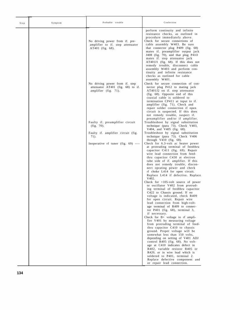
S t e p Symptom Probab le t roub le
No driving power from if. pre-amplifier to if. step attenuatorAT401 (fig. 68).
No driving power from if. stepattenuator AT401 (fig. 68) to if.amplifier (fig. 71).
Faulty if . preamplifier circuit(fig. 70).
Faulty if. amplifier circuit (fig.71).
Inoperative rf tuner (fig. 69) ----
Confec t ion
perform continuity and infiniteresistance checks, as outlined inprocedure immediately above.
Check for secure connections ofcable assembly W403. Be surethat connector plug P409 (fig. 68)mates if. preamplifier output jackJ408 (fig. 70), and that plug P41Omates if. step attenuator jackAT401J1 (fig. 68). If this does notremedy trouble, disconnect cableassembly W403 and perform con-tinuity and infinite resistancechecks as outlined for cableassembly W401.
Check for secure connection of con-nector plug P412 to mating jackAT401J2 on if. step attenuator(fig. 68). Opposite end of thiscoaxial cable is soldered totermination CP411 at input to if.amplifier (fig. 71). Check andrepair solder connection if opencircuit is suspected. If this doesnot remedy trouble, suspect if.preamplifier and/or if amplifier .
Troubleshoot by signal substitutiontechnique (para 73). Check V403,V404, and V405 (fig. 68).
Troubleshoot by signal substitutiontechnique (para 73). Check V406through V410 (fig. 68).
Check for 6.3-volt ac heater powerat protruding terminal of feedthrucapacitor C411 (fig. 69). Repairwire lead connection from feed-thru capacitor C430 at electrontube side of if. amplifier. If thisdoes not remedy trouble, discon-nect oprating power and checkrf choke L414 for open circuit.Replace L414 if defective. ReplaceV402.
Check for +105-volt source of powerto oscillator V402 from protrud-ing terminal of feedthru capacitorC422 to Chassis ground. If novoltage is indicated, check R409for open circuit. Repair wirelead connection from high-volt-age terminal of R409 to connec-tor P401 (fig. 68), terminal 3,if necessary.
Check for B+ voltage to rf ampli-fier V401 by measuring voltagefrom protruding terminal of feed-thru capacitor C410 to chassisground. Proper voltage will besomewhat less than 150 volts,depending on setting of V401 ADJcontrol R405 (fig. 68). No volt-age at C410 indicates defect inR402, variable resistor R405 orR420, or in wire lead which issoldered to P401, terminal 2.Replace defective component andor repair lead connection.
134
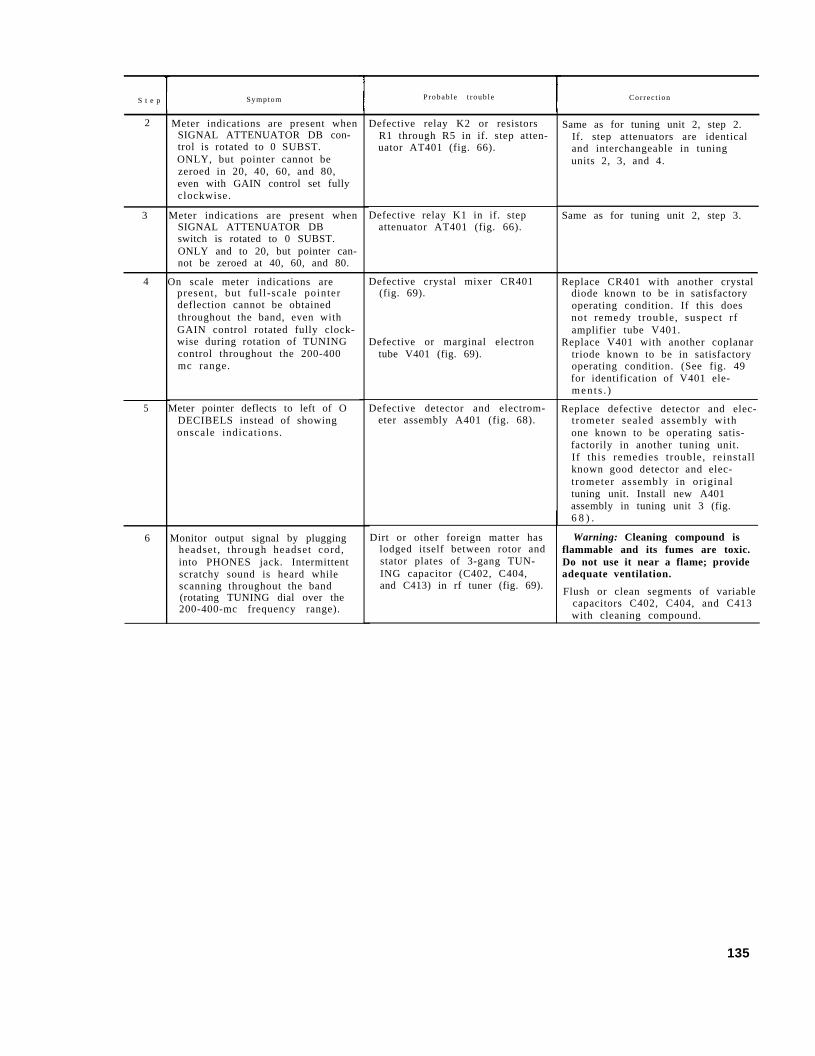
S t e p Symptom Probab le t roub le Cor rec t ion
2 Meter indications are present whenSIGNAL ATTENUATOR DB con-trol is rotated to 0 SUBST.ONLY, but pointer cannot bezeroed in 20, 40, 60, and 80,even with GAIN control set fullyclockwise.
3 Meter indications are present whenSIGNAL ATTENUATOR DBswitch is rotated to 0 SUBST.ONLY and to 20, but pointer can-not be zeroed at 40, 60, and 80.
Defective relay K2 or resistorsR1 through R5 in if. step atten-uator AT401 (fig. 66).
Defective relay K1 in if. stepattenuator AT401 (fig. 66).
Same as for tuning unit 2, step 2.If. step attenuators are identicaland interchangeable in tuningunits 2, 3, and 4.
Same as for tuning unit 2, step 3.
4
5
6
On scale meter indications arepresent , but full-scale pointerdeflection cannot be obtainedthroughout the band, even withGAIN control rotated fully clock-wise during rotation of TUNINGcontrol throughout the 200-400mc range.
Meter pointer deflects to left of ODECIBELS instead of showingonscale indications.
Monitor output signal by pluggingheadset , through headset cord,into PHONES jack. Intermittentscratchy sound is heard whilescanning throughout the band(rotating TUNING dial over the200-400-mc frequency range).
Defective crystal mixer CR401(fig. 69).
Defective or marginal electrontube V401 (fig. 69).
Replace CR401 with another crystaldiode known to be in satisfactoryoperating condition. If this doesnot remedy trouble, suspect rfamplifier tube V401.
Replace V401 with another coplanartriode known to be in satisfactoryoperating condition. (See fig. 49for identification of V401 ele-m e n t s . )
Defective detector and electrom-eter assembly A401 (fig. 68).
Replace defective detector and elec-trometer sealed assembly withone known to be operating satis-factorily in another tuning unit.If this remedies trouble, reinstal lknown good detector and elec-trometer assembly in originaltuning unit. Install new A401assembly in tuning unit 3 (fig.6 8 ) .
Dirt or other foreign matter has Warning: Cleaning compound islodged itself between rotor and flammable and its fumes are toxic.stator plates of 3-gang TUN- Do not use it near a flame; provideING capacitor (C402, C404, adequate ventilation.and C413) in rf tuner (fig. 69).
Flush or clean segments of variablecapacitors C402, C404, and C413with cleaning compound.
135

This page left blank intentionally.
1 3 6
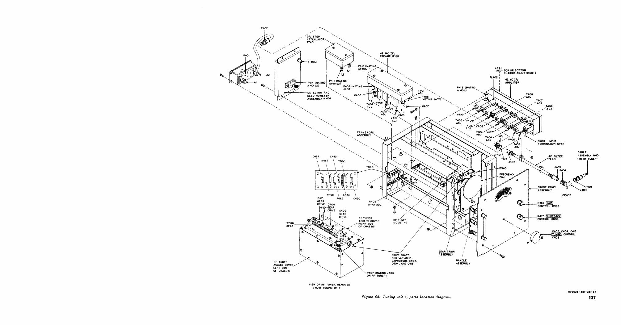
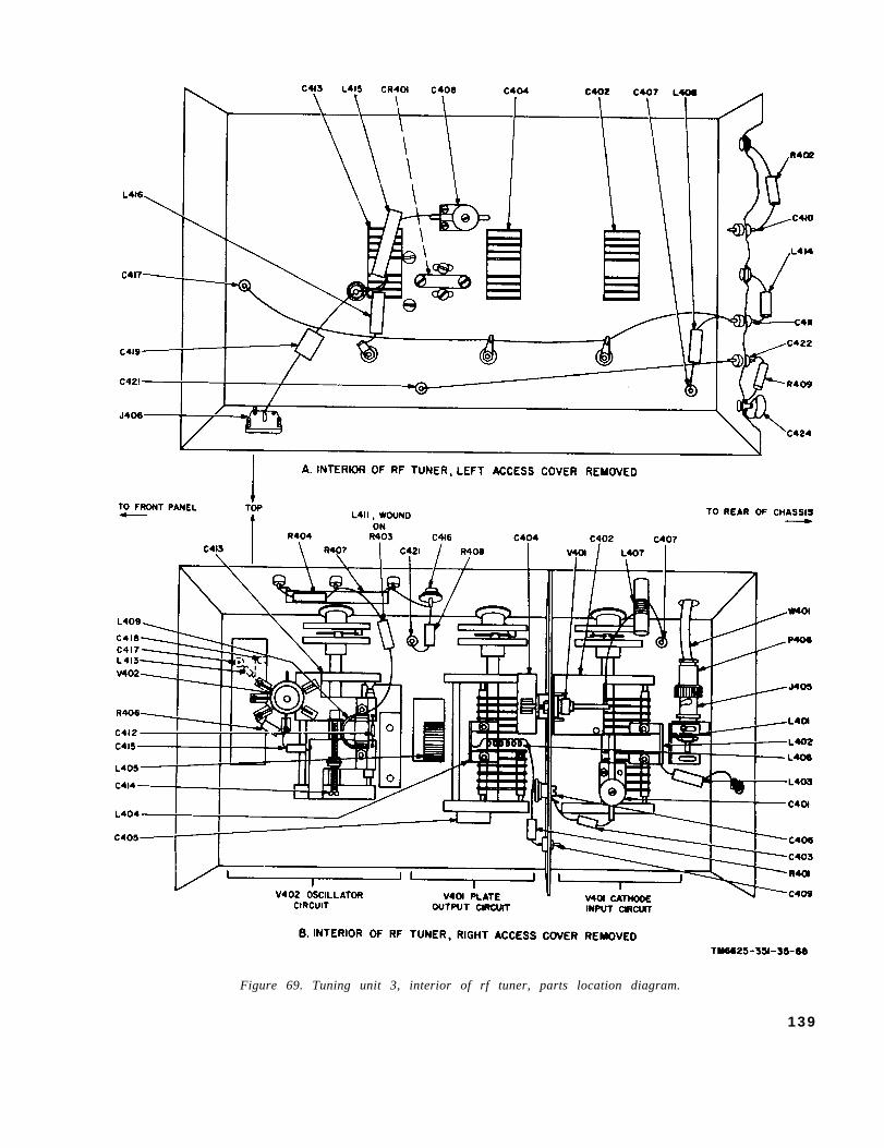
Figure 69. Tuning unit 3, interior of rf tuner, parts location diagram.
139
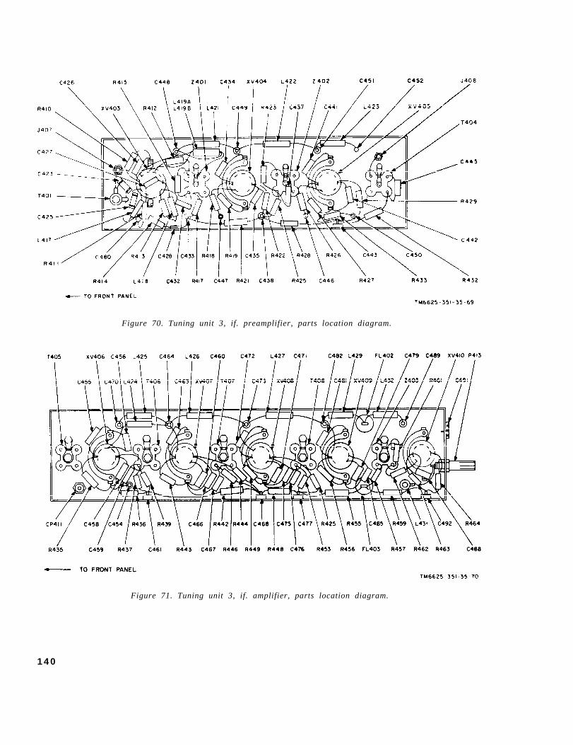
Figure 70. Tuning unit 3, if. preamplifier, parts location diagram.
Figure 71. Tuning unit 3, if. amplifier, parts location diagram.
1 4 0
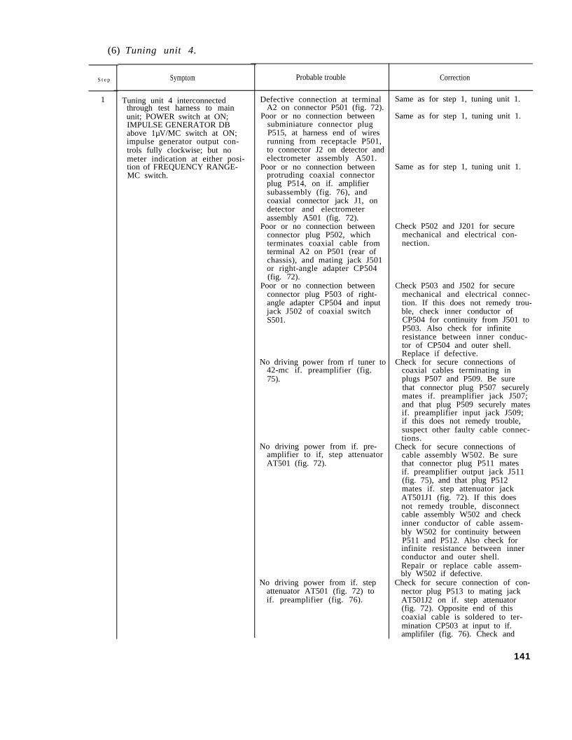
(6) Tuning unit 4.
S t e p
1
Symptom
Tuning unit 4 interconnectedthrough test harness to mainunit; POWER switch at ON;IMPULSE GENERATOR DBabove 1µV/MC switch at ON;impulse generator output con-trols fully clockwise; but nometer indication at either posi-tion of FREQUENCY RANGE-MC switch.
Probable trouble
Defective connection at terminalA2 on connector P501 (fig. 72).
Poor or no connection betweensubminiature connector plugP515, at harness end of wiresrunning from receptacle P501,to connector J2 on detector andelectrometer assembly A501.
Poor or no connection betweenprotruding coaxial connectorplug P514, on if. amplifiersubassembly (fig. 76), andcoaxial connector jack J1, ondetector and electrometerassembly A501 (fig. 72).
Poor or no connection betweenconnector plug P502, whichterminates coaxial cable fromterminal A2 on P501 (rear ofchassis), and mating jack J501or right-angle adapter CP504(fig. 72).
Poor or no connection betweenconnector plug P503 of right-angle adapter CP504 and inputjack J502 of coaxial switchS501.
No driving power from rf tuner to42-mc if. preamplifier (fig.75).
No driving power from if. pre-amplifier to if, step attenuatorAT501 (fig. 72).
No driving power from if. stepattenuator AT501 (fig. 72) toif. preamplifier (fig. 76).
Correction
Same as for step 1, tuning unit 1.
Same as for step 1, tuning unit 1.
Same as for step 1, tuning unit 1.
Check P502 and J201 for securemechanical and electrical con-nection.
Check P503 and J502 for securemechanical and electrical connec-tion. If this does not remedy trou-ble, check inner conductor ofCP504 for continuity from J501 toP503. Also check for infiniteresistance between inner conduc-tor of CP504 and outer shell.Replace if defective.
Check for secure connections ofcoaxial cables terminating inplugs P507 and P509. Be surethat connector plug P507 securelymates if. preamplifier jack J507;and that plug P509 securely matesif. preamplifier input jack J509;if this does not remedy trouble,suspect other faulty cable connec-tions.
Check for secure connections ofcable assembly W502. Be surethat connector plug P511 matesif. preamplifier output jack J511(fig. 75), and that plug P512mates if. step attenuator jackAT501J1 (fig. 72). If this doesnot remedy trouble, disconnectcable assembly W502 and checkinner conductor of cable assem-bly W502 for continuity betweenP511 and P512. Also check forinfinite resistance between innerconductor and outer shell.Repair or replace cable assem-bly W502 if defective.
Check for secure connection of con-nector plug P513 to mating jackAT501J2 on if. step attenuator(fig. 72). Opposite end of thiscoaxial cable is soldered to ter-mination CP503 at input to if.amplifiler (fig. 76). Check and
141
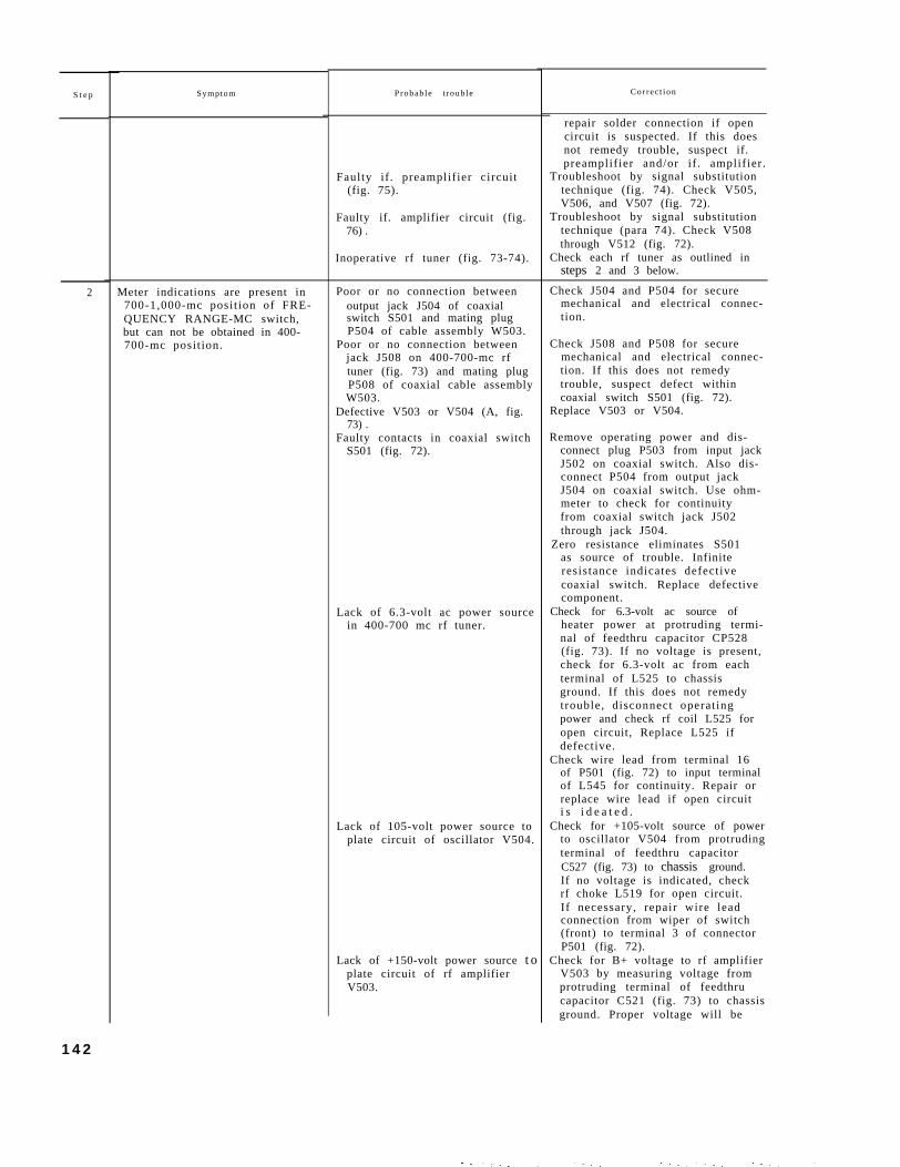
S t e p
2
1 4 2
Symptom
Meter indications are present in700-1,000-mc posit ion of FRE-QUENCY RANGE-MC switch,but can not be obtained in 400-700-mc posit ion.
Probab le t roub le
Faulty if . preamplifier circuit(fig. 75).
Faulty if. amplifier circuit (fig.76) .
Inoperative rf tuner (fig. 73-74).
Poor or no connection betweenoutput jack J504 of coaxialswitch S501 and mating plugP504 of cable assembly W503.
Poor or no connection betweenjack J508 on 400-700-mc rftuner (fig. 73) and mating plugP508 of coaxial cable assemblyW503.
Defective V503 or V504 (A, fig.73) .
Faulty contacts in coaxial switchS501 (fig. 72).
Lack of 6.3-volt ac power sourcein 400-700 mc rf tuner.
Lack of 105-volt power source toplate circuit of oscillator V504.
Lack of +150-volt power source t oplate circuit of rf amplifierV503.
Correc t ion
repair solder connection if opencircuit is suspected. If this doesnot remedy trouble, suspect if.preamplifier and/or if . amplifier .
Troubleshoot by signal substitutiontechnique (fig. 74). Check V505,V506, and V507 (fig. 72).
Troubleshoot by signal substitutiontechnique (para 74). Check V508through V512 (fig. 72).
Check each rf tuner as outlined insteps 2 and 3 below.
Check J504 and P504 for securemechanical and electrical connec-tion.
Check J508 and P508 for securemechanical and electrical connec-tion. If this does not remedytrouble, suspect defect withincoaxial switch S501 (fig. 72).
Replace V503 or V504.
Remove operating power and dis-connect plug P503 from input jackJ502 on coaxial switch. Also dis-connect P504 from output jackJ504 on coaxial switch. Use ohm-meter to check for continuityfrom coaxial switch jack J502through jack J504.
Zero resistance eliminates S501as source of trouble. Infiniteresistance indicates defectivecoaxial switch. Replace defectivecomponent.
Check for 6.3-volt ac source ofheater power at protruding termi-nal of feedthru capacitor CP528(fig. 73). If no voltage is present,check for 6.3-volt ac from eachterminal of L525 to chassisground. If this does not remedytrouble, disconnect operat ingpower and check rf coil L525 foropen circuit, Replace L525 ifdefective.
Check wire lead from terminal 16of P501 (fig. 72) to input terminalof L545 for continuity. Repair orreplace wire lead if open circuiti s i d e a t e d .
Check for +105-volt source of powerto oscillator V504 from protrudingterminal of feedthru capacitorC527 (fig. 73) to chassis ground.If no voltage is indicated, checkrf choke L519 for open circuit.If necessary, repair wire leadconnection from wiper of switch(front) to terminal 3 of connectorP501 (fig. 72).
Check for B+ voltage to rf amplifierV503 by measuring voltage fromprotruding terminal of feedthrucapacitor C521 (fig. 73) to chassisground. Proper voltage will be
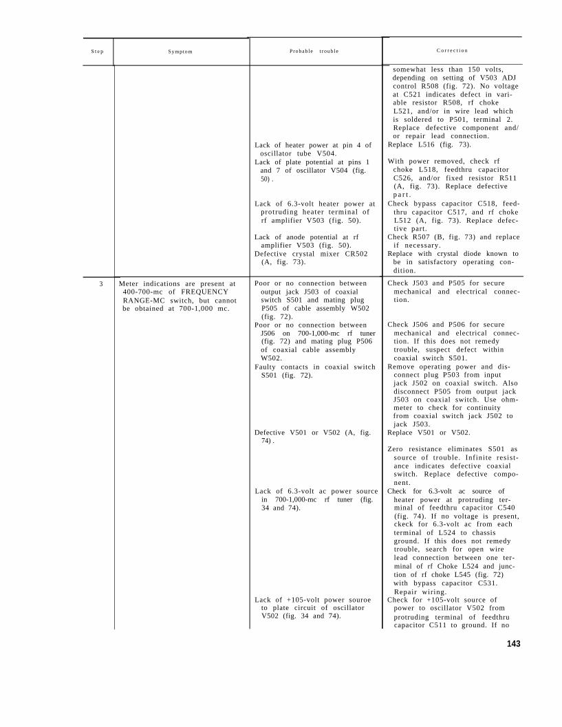
S t e p Symptom Probab le t roub le
3 Meter indications are present at400-700-mc of FREQUENCYRANGE-MC switch, but cannotbe obtained at 700-1,000 mc.
Lack of heater power at pin 4 ofoscillator tube V504.
Lack of plate potential at pins 1and 7 of oscillator V504 (fig.50) .
Lack of 6.3-volt heater power atprotruding heater terminal ofrf amplifier V503 (fig. 50).
Lack of anode potential at rfamplifier V503 (fig. 50).
Defective crystal mixer CR502(A, fig. 73).
Poor or no connection betweenoutput jack J503 of coaxialswitch S501 and mating plugP505 of cable assembly W502(fig. 72).
Poor or no connection betweenJ506 on 700-1,000-mc rf tuner(fig. 72) and mating plug P506of coaxial cable assemblyW502.
Faulty contacts in coaxial switchS501 (fig. 72).
Defective V501 or V502 (A, fig.74) .
Lack of 6.3-volt ac power sourcein 700-1,000-mc rf tuner (fig.34 and 74).
Lack of +105-volt power souroeto plate circuit of oscillatorV502 (fig. 34 and 74).
C o r r e c t i o n
somewhat less than 150 volts,depending on setting of V503 ADJcontrol R508 (fig. 72). No voltageat C521 indicates defect in vari-able resistor R508, rf chokeL521, and/or in wire lead whichis soldered to P501, terminal 2.Replace defective component and/or repair lead connection.
Replace L516 (fig. 73).
With power removed, check rfchoke L518, feedthru capacitorC526, and/or fixed resistor R511(A, fig. 73). Replace defectivep a r t .
Check bypass capacitor C518, feed-thru capacitor C517, and rf chokeL512 (A, fig. 73). Replace defec-tive part.
Check R507 (B, fig. 73) and replaceif necessary.
Replace with crystal diode known tobe in satisfactory operating con-dition.
Check J503 and P505 for securemechanical and electrical connec-tion.
Check J506 and P506 for securemechanical and electrical connec-tion. If this does not remedytrouble, suspect defect withincoaxial switch S501.
Remove operating power and dis-connect plug P503 from inputjack J502 on coaxial switch. Alsodisconnect P505 from output jackJ503 on coaxial switch. Use ohm-meter to check for continuityfrom coaxial switch jack J502 tojack J503.
Replace V501 or V502.
Zero resistance eliminates S501 assource of trouble. Infinite resist-ance indicates defective coaxialswitch. Replace defective compo-nent.
Check for 6.3-volt ac source ofheater power at protruding ter-minal of feedthru capacitor C540(fig. 74). If no voltage is present,ckeck for 6.3-volt ac from eachterminal of L524 to chassisground. If this does not remedytrouble, search for open wirelead connection between one ter-minal of rf Choke L524 and junc-tion of rf choke L545 (fig. 72)with bypass capacitor C531.Repair wiring.
Check for +105-volt source ofpower to oscillator V502 fromprotruding terminal of feedthrucapacitor C511 to ground. If no
143
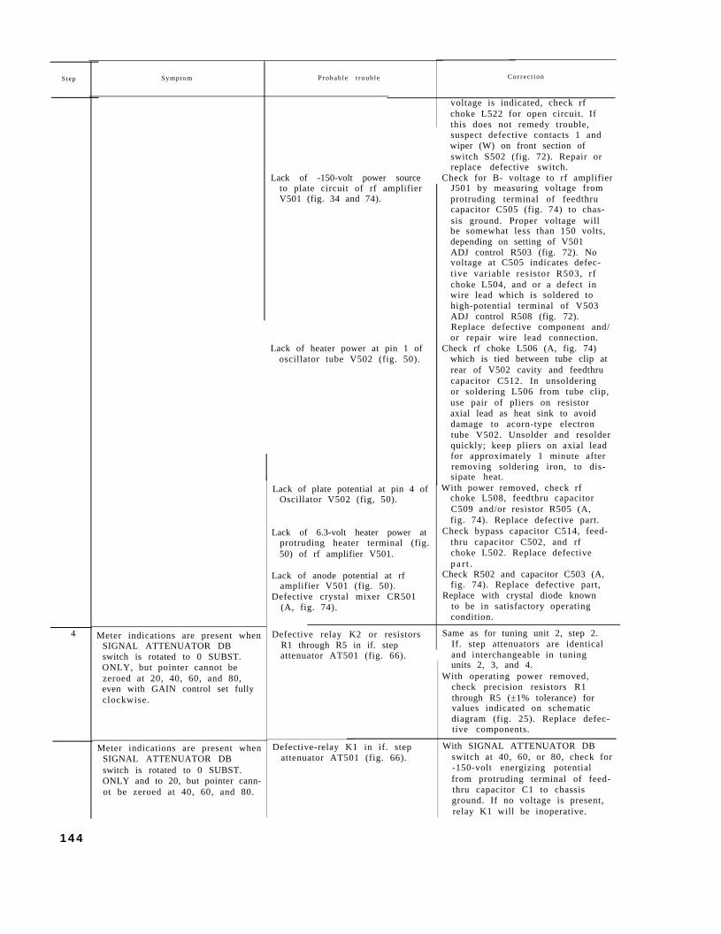
Step Symptom Probab le t roub le Cor rec t ion
voltage is indicated, check rfchoke L522 for open circuit. Ifthis does not remedy trouble,suspect defective contacts 1 andwiper (W) on front section ofswitch S502 (fig. 72). Repair orreplace defective switch.
Lack of -150-volt power source Check for B- voltage to rf amplifierto plate circuit of rf amplifier J501 by measuring voltage fromV501 (fig. 34 and 74). protruding terminal of feedthru
capacitor C505 (fig. 74) to chas-sis ground. Proper voltage willbe somewhat less than 150 volts,depending on setting of V501
4 Meter indications are present whenSIGNAL ATTENUATOR DBswitch is rotated to 0 SUBST.ONLY, but pointer cannot bezeroed at 20, 40, 60, and 80,even with GAIN control set fullyclockwise.
Meter indications are present whenSIGNAL ATTENUATOR DBswitch is rotated to 0 SUBST.ONLY and to 20, but pointer cann-ot be zeroed at 40, 60, and 80.
Lack of heater power at pin 1 ofoscillator tube V502 (fig. 50).
Lack of plate potential at pin 4 ofOscillator V502 (fig, 50).
Lack of 6.3-volt heater power atprotruding heater terminal (fig.50) of rf amplifier V501.
Lack of anode potential at rfamplifier V501 (fig. 50).
Defective crystal mixer CR501(A, fig. 74).
Defective relay K2 or resistorsR1 through R5 in if. stepattenuator AT501 (fig. 66).
Defective-relay K1 in if. stepattenuator AT501 (fig. 66).
ADJ control R503 (fig. 72). Novoltage at C505 indicates defec-t ive variable resistor R503, rfchoke L504, and or a defect inwire lead which is soldered tohigh-potential terminal of V503ADJ control R508 (fig. 72).Replace defective component and/or repair wire lead connection.
Check rf choke L506 (A, fig. 74)which is tied between tube clip atrear of V502 cavity and feedthrucapacitor C512. In unsolderingor soldering L506 from tube clip,use pair of pliers on resistoraxial lead as heat sink to avoiddamage to acorn-type electrontube V502. Unsolder and resolderquickly; keep pliers on axial leadfor approximately 1 minute afterremoving soldering iron, to dis-sipate heat.
With power removed, check rfchoke L508, feedthru capacitorC509 and/or resistor R505 (A,fig. 74). Replace defective part.
Check bypass capacitor C514, feed-thru capacitor C502, and rfchoke L502. Replace defectivep a r t .
Check R502 and capacitor C503 (A,fig. 74). Replace defective part,
Replace with crystal diode knownto be in satisfactory operatingcondition.
Same as for tuning unit 2, step 2.If. step attenuators are identicaland interchangeable in tuningunits 2, 3, and 4.
With operating power removed,check precision resistors R1through R5 (±1% tolerance) forvalues indicated on schematicdiagram (fig. 25). Replace defec-tive components.
With SIGNAL ATTENUATOR DBswitch at 40, 60, or 80, check for-150-volt energizing potentialfrom protruding terminal of feed-thru capacitor C1 to chassisground. If no voltage is present,relay K1 will be inoperative.
1 4 4
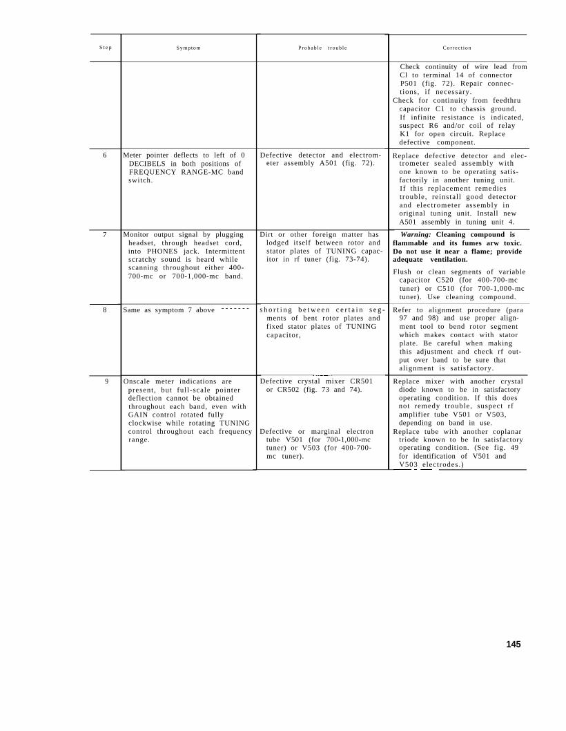
S t e p
6
7
8
9
Symptom
Meter pointer deflects to left of 0DECIBELS in both positions ofFREQUENCY RANGE-MC bandswitch.
Monitor output signal by pluggingheadset, through headset cord,into PHONES jack. Intermittentscratchy sound is heard whilescanning throughout either 400-700-mc or 700-1,000-mc band.
Same as symptom 7 above - - - - - - -
Onscale meter indications arepresent , but full-scale pointerdeflection cannot be obtainedthroughout each band, even withGAIN control rotated fullyclockwise while rotating TUNINGcontrol throughout each frequencyrange.
Probab le t roub le
Defective detector and electrom-eter assembly A501 (fig. 72).
Dirt or other foreign matter haslodged itself between rotor andstator plates of TUNING capac-itor in rf tuner (fig. 73-74).
s h o r t i n g b e t w e e n c e r t a i n s e g -ments of bent rotor plates andfixed stator plates of TUNINGcapacitor,
Defective crystal mixer CR501or CR502 (fig. 73 and 74).
Defective or marginal electrontube V501 (for 700-1,000-mctuner) or V503 (for 400-700-mc tuner).
Correc t ion
Check continuity of wire lead fromCl to terminal 14 of connectorP501 (fig. 72). Repair connec-tions, if necessary.
Check for continuity from feedthrucapacitor C1 to chassis ground.If infinite resistance is indicated,suspect R6 and/or coil of relayK1 for open circuit. Replacedefective component.
Replace defective detector and elec-trometer sealed assembly withone known to be operating satis-factorily in another tuning unit.If this replacement remediestrouble, reinstal l good detectorand electrometer assembly inoriginal tuning unit. Install newA501 assembly in tuning unit 4.
Warning: Cleaning compound isflammable and its fumes arw toxic.Do not use it near a flame; provideadequate ventilation.
Flush or clean segments of variablecapacitor C520 (for 400-700-mctuner) or C510 (for 700-1,000-mctuner). Use cleaning compound.
Refer to alignment procedure (para97 and 98) and use proper align-ment tool to bend rotor segmentwhich makes contact with statorplate. Be careful when makingthis adjustment and check rf out-put over band to be sure thatalignment is satisfactory.
Replace mixer with another crystaldiode known to be in satisfactoryoperating condition. If this doesnot remedy trouble, suspect rfamplifier tube V501 or V503,depending on band in use.
Replace tube with another coplanartriode known to be In satisfactoryoperating condition. (See fig. 49for identification of V501 andV503 electrodes.)
145

This page left blank intentionally.
146
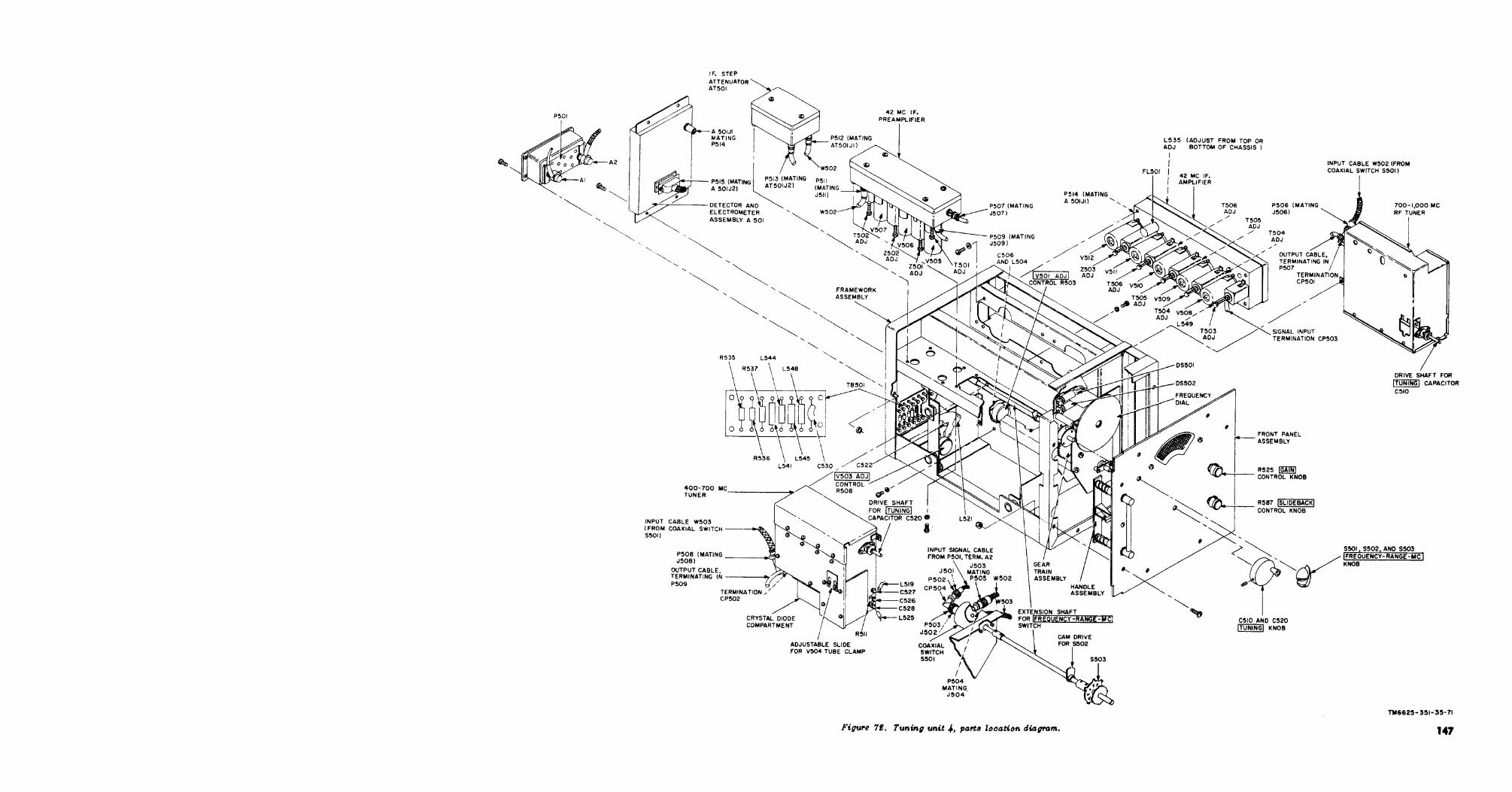
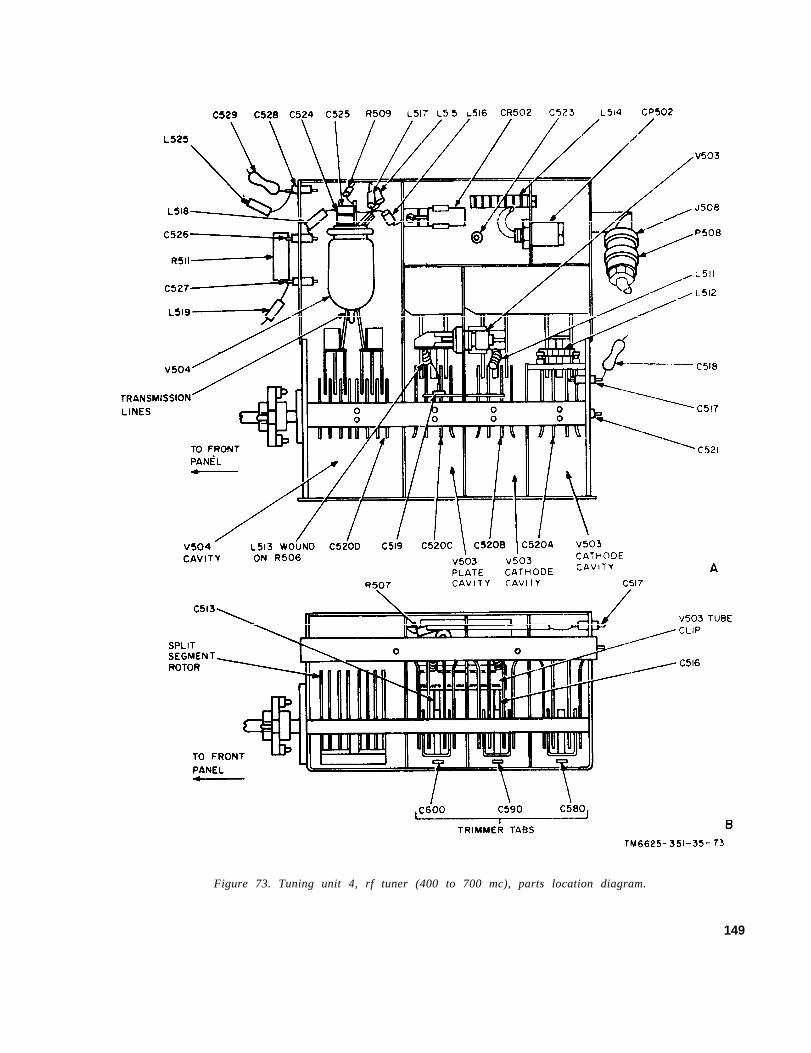
Figure 73. Tuning unit 4, rf tuner (400 to 700 mc), parts location diagram.
149
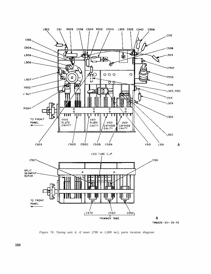
Figure 74. Tuning unit 4, rf tuner (700 to 1,000 mc), parts location diagram.
150
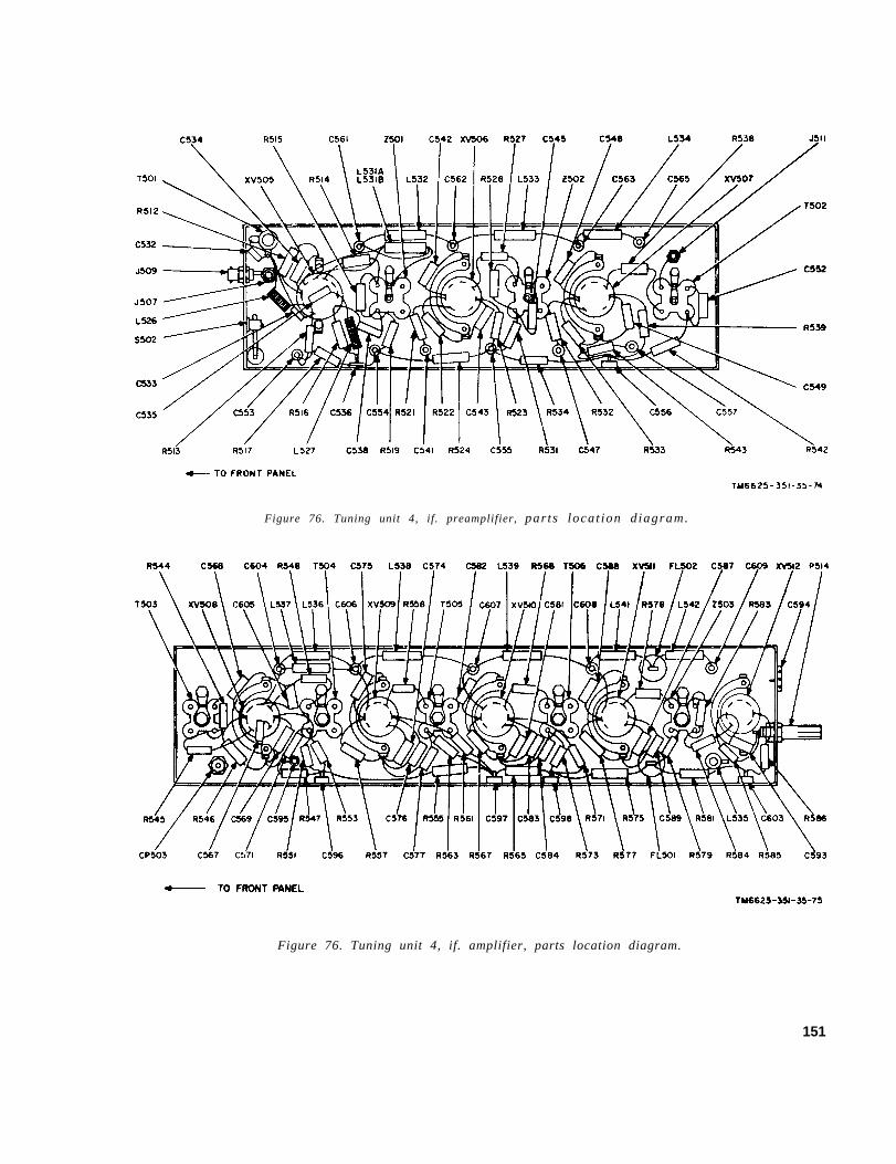
Figure 76. Tuning unit 4, if. preamplifier, par ts loca t ion d iagram.
Figure 76. Tuning unit 4, if. amplifier, parts location diagram.
151
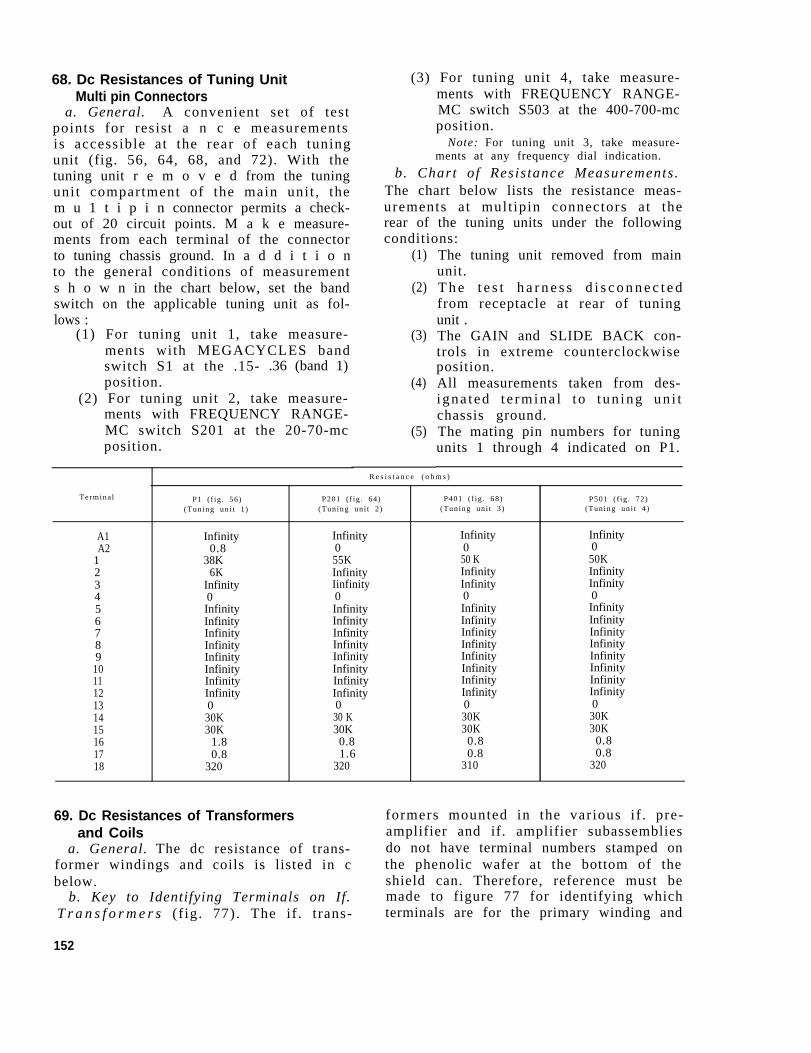
68. Dc Resistances of Tuning UnitMulti pin Connectors
a. General. A convenient set of testpoints for resist a n c e measurementsis accessible at the rear of each tuningunit (fig. 56, 64, 68, and 72). With thetuning unit r e m o v e d from the tuningunit compartment of the main unit , them u 1 t i p i n connector permits a check-out of 20 circuit points. M a k e measure-ments from each terminal of the connectorto tuning chassis ground. In a d d i t i o nto the general conditions of measurements h o w n in the chart below, set the bandswitch on the applicable tuning unit as fol-lows :
(1) For tuning unit 1, take measure-ments with MEGACYCLES bandswitch S1 at the .15- .36 (band 1)position.
(2) For tuning unit 2, take measure-ments with FREQUENCY RANGE-MC switch S201 at the 20-70-mcposition.
Termina l
A1A2
123456789
101112131415161718
P1 ( f ig . 56)(Tun ing un i t 1 )
Infinity0.8
38K6K
Infinity0InfinityInfinityInfinityInfinityInfinityInfinityInfinityInfinity030K30K
1.80.8
320
(3) For tuning unit 4, take measure-ments with FREQUENCY RANGE-MC switch S503 at the 400-700-mcposition.
Note: For tuning unit 3, take measure-ments at any frequency dial indication.
b. Chart of Resistance Measurements.The chart below lists the resistance meas-urements at mult ipin connectors at therear of the tuning units under the followingconditions:
(1)
(2)
(3)
(4)
(5)
The tuning unit removed from mainunit.T h e t e s t h a r n e s s d i s c o n n e c t e dfrom receptacle at rear of tuningunit .The GAIN and SLIDE BACK con-trols in extreme counterclockwiseposition.All measurements taken from des-igna ted t e rmina l t o tun ing un i tchassis ground.The mating pin numbers for tuningunits 1 through 4 indicated on P1.
R e s i s t a n c e ( o h m s )
P201 ( f ig . 64)(Tun ing un i t 2 )
Infinity055KInfinityIinfinity0InfinityInfinityInfinityInfinityInfinityInfinityInfinityInfinity030 K30K0.81.6
320
P401 ( f ig . 68)(Tun ing un i t 3 )
Infinity050 KInfinityInfinity0InfinityInfinityInfinityInfinityInfinityInfinityInfinityInfinity030K30K0.80.8
310
P501 ( f ig . 72)(Tun ing un i t 4 )
Infinity050KInfinityInfinity0InfinityInfinityInfinityInfinityInfinityInfinityInfinityInfinity030K30K
0.80.8
320
69. Dc Resistances of Transformers formers mounted in the various if . pre-and Coils amplifier and if. amplifier subassemblies
a. General. The dc resistance of trans- do not have terminal numbers stamped onformer windings and coils is listed in c the phenolic wafer at the bottom of thebelow. shield can. Therefore, reference must be
b. Key to Identifying Terminals on If. made to figure 77 for identifying whichT r a n s f o r m e r s (f ig. 77). The if . t rans- terminals are for the primary winding and
152
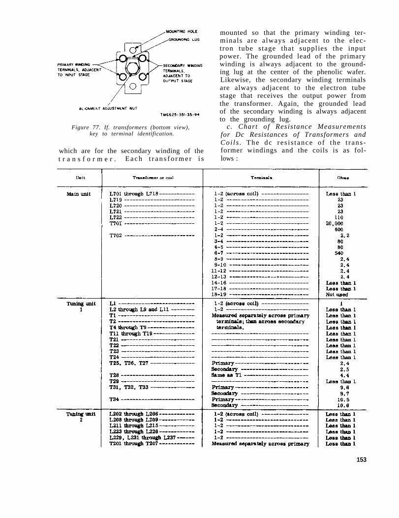
Figure 77. If. transformers (bottom view),key to terminal identification.
which are for the secondary winding of thet r a n s f o r m e r . E a c h t r a n s f o r m e r i s
mounted so that the primary winding ter-minals are always adjacent to the elec-tron tube stage that supplies the inputpower. The grounded lead of the primarywinding is always adjacent to the ground-ing lug at the center of the phenolic wafer.Likewise, the secondary winding terminalsare always adjacent to the electron tubestage that receives the output power fromthe transformer. Again, the grounded leadof the secondary winding is always adjacentto the grounding lug.
c. Chart of Resistance Measurementsfor Dc Resistances of Transformers andCoi l s . The dc res i s t ance o f the t r ans -former windings and the coils is as fol-lows :
153
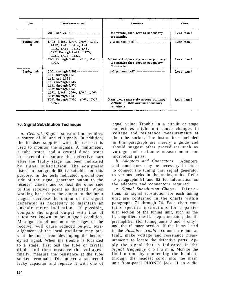
70. Signal Substitution Technique
a. General. Signal substitution requiresa source of if. and rf signals. In addition,the headset supplied with the test set isused to monitor the signals. A multimeter,a tube tester, and a crystal diode testerare needed to isolate the defective partafter the faulty stage has been indicatedby s igna l subs t i tu t ion . The equ ipmen tlisted in paragraph 65 is suitable for thispurpose. In the tests indicated, ground oneside of the signal generator output to thereceiver chassis and connect the other sideto the receiver point as directed. Whenworking back from the output to the inputstages, decrease the output of the signalgenera to r a s necessa ry to ma in ta in anonsca le me te r ind ica t ion . If possible,compare the s ignal output with that ofa test set known to be in good condition.Misalignment of one or more stages of thereceiver will cause reduced output. Mis-alignment of the local oscillator may pre-vent the tuner from developing the hetero-dyned signal. When the trouble is localizedto a stage, first test the tube or crystald iode and then measure the vo l t ages ;finally, measure the resistance at the tubesocket terminals. Disconnect a suspectedleaky capacitor and replace it with one of
154
equal value. Trouble in a circuit or stagesometimes might not cause changes involtage and resistance measurements atthe tube socket. The instructions includedin this paragraph are merely a guide andshould suggest other procedures such asvoltage and resi tance measurements onindividual parts.
b. Adapters and Connectors. Adaptersand connectors may be necessary in orderto connect the tuning unit signal generatorto various jacks in the tuning units. Referto paragraphs 81 and 82 for information onthe adapters and connectors required.
c. Signal Substitution Charts. D i r e c -tions for signal substitution for each tuningunit are contained in the charts withinparagraphs 71 through 74. Each chart con-tains specif ic instruct ions for a part ic-ular section of the tuning unit, such as theif. amplifier, the if. step attenuator, the if.preamplifier (for tuning units 3 and 4 only),and the rf tuner section. If the items listedin the Possible trouble column are not atfault, make voltage and resistance meas-urements to locate the defective parts. Ap-ply the s ignal that is indicated in theSignal frequency c o l u m n. Monitor thefinal output by connect ing the headset ,through the headset cord, into the mainunit front-panel PHONES jack. If an audio
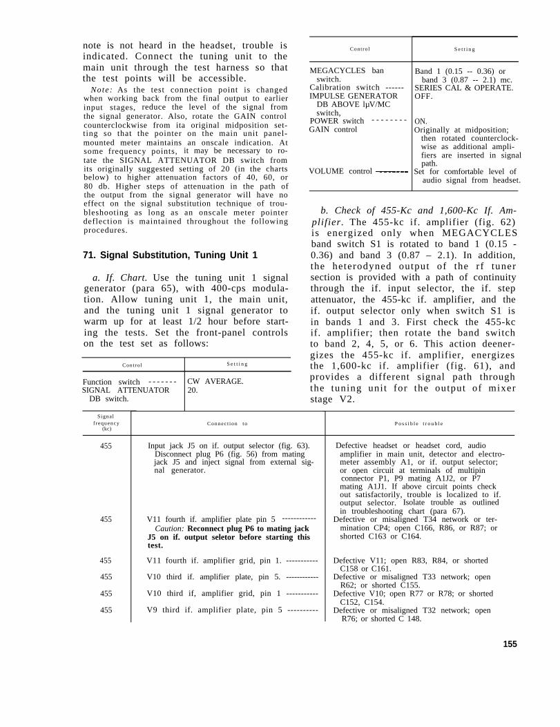
note is not heard in theindicated. Connect the
headset, trouble istuning unit to the
main unit through the test harness so thatthe test points will be accessible.
Note: As the test connection point is changedwhen working back from the final output to earlierinput stages, reduce the level of the signal fromthe signal generator. Also, rotate the GAIN controlcounterclockwise from ita original midposition set-ting so that the pointer on the main unit panel-mounted meter maintains an onscale indication. Atsome frequency points, it may be necessary to ro-tate the SIGNAL ATTENUATOR DB switch fromits originally suggested setting of 20 (in the chartsbelow) to higher attenuation factors of 40, 60, or80 db. Higher steps of attenuation in the path ofthe output from the signal generator will have noeffect on the signal substitution technique of trou-bleshooting as long as an onscale meter pointerdeflection is maintained throughout the followingprocedures.
71. Signal Substitution, Tuning Unit 1
a. If. Chart. Use the tuning unit 1 signalgenerator (para 65), with 400-cps modula-tion. Allow tuning unit 1, the main unit,and the tuning unit 1 signal generator towarm up for at least 1/2 hour before start-ing the tests. Set the front-panel controlson the test set as follows:
Contro l S e t t i n g
Function switch - - - - - - - CW AVERAGE.SIGNAL ATTENUATOR 20.
DB switch.
Signalf requency
(kc)
455
455
455
455
455
455
Contro l
MEGACYCLES banswitch.
Calibration switch ------IMPULSE GENERATOR
DB ABOVE lµV/MCswitch,
POWER switch - - - - - - - -GAIN control
VOLUME control
S e t t i n g
Band 1 (0.15 -- 0.36) orband 3 (0.87 -- 2.1) mc.
SERIES CAL & OPERATE.OFF.
ON.Originally at midposition;
then rotated counterclock-wise as additional ampli-fiers are inserted in signalpath.
Set for comfortable level ofaudio signal from headset.
Connec t ion to
b. Check of 455-Kc and 1,600-Kc If. Am-plifier. The 455-kc if. amplifier (fig. 62)is energized only when MEGACYCLESband switch S1 is rotated to band 1 (0.15 -0.36) and band 3 (0.87 – 2.1). In addition,the heterodyned output of the rf tunersection is provided with a path of continuitythrough the if. input selector, the if. stepattenuator, the 455-kc if. amplifier, and theif. output selector only when switch S1 isin bands 1 and 3. First check the 455-kcif. amplifier; then rotate the band switchto band 2, 4, 5, or 6. This action deener-gizes the 455-kc if. amplifier, energizesthe 1,600-kc if. amplifier (fig. 61), andprovides a different signal path throughthe tuning uni t for the output of mixerstage V2.
Input jack J5 on if. output selector (fig. 63).Disconnect plug P6 (fig. 56) from matingjack J5 and inject signal from external sig-nal generator.
V11 fourth if. amplifier plate pin 5 ------------Caution: Reconnect plug P6 to mating jack
J5 on if. output seletor before starting thistest.
V11 fourth if. amplifier grid, pin 1. -----------
V10 third if. amplifier plate, pin 5. ------------
V10 third if, amplifier grid, pin 1 -----------
V9 third if. amplifier plate, pin 5 ----------
P o s s i b l e t r o u b l e
Defective headset or headset cord, audioamplifier in main unit, detector and electro-meter assembly A1, or if. output selector;or open circuit at terminals of multipinconnector P1, P9 mating A1J2, or P7mating A1J1. If above circuit points checkout satisfactorily, trouble is localized to if.output selector. Isolate trouble as outlinedin troubleshooting chart (para 67).
Defective or misaligned T34 network or ter-mination CP4; open C166, R86, or R87; orshorted C163 or C164.
Defective V11; open R83, R84, or shortedC158 or C161.
Defective or misaligned T33 network; openR62; or shorted C155.
Defective V10; open R77 or R78; or shortedC152, C154.
Defective or misaligned T32 network; openR76; or shorted C 148.
155
Signalf requency
( k c )
455
455
455
455
455
1,600
1,600
1,600
1,600
1,600
1,600
1,600
1,600
1,600
1,600
1,600
Connec t ion to Poss ib l e t roub le
V9 second if. amplifier grid, pin 1 - - - - - - - - -
V8 first if. amplifier plate, pin 5 ----- ----- -
V8 first if. amplifier grid, pin 1. --------------
If. interstate transformer T29, terminal 4(fig. 62).
V2 mixer plate, pin 1 ------ ------ --------
Input jack J4 on if. output selector (fig. 63).Disconnect plug P5 from mating jack J4 andinject signal from external signal generator.
V7 fourth if. amplifier plate, pin 5 -----------Caution: Reconnect plug P5 to mating jack
J4 on if. output selector before starting thistest.
V7 fourth if. amplifier grid, pin 1 - - - - - - - - - -
V6 third if. amplifier grid, pin 5 - - - - - - - - - - -
V6 third if. amplifier grid, pin 1 -------------
V5 second if. amplifier plate, pin 5 - - - - - - - - -
V5 second if. amplifier grid, pin 1 -----------
V4 first if. amplifier plate, pin 5 - - - - - - - - - - -
V4 first if. amplifier grid, pin 1 ------ -----
If. interstate transformer T24 at ungroundedterminal of primary winding.
V2 mixer plate, pin 1 ------ ------ ------ ---
Defective V9. open R72 or R73: or shortedC145, C147.
Defective or misaligned T31 network; openR69, R71, R88, or K89, feedthru capacitorC142, or coupling capacitor C144: shortedC137, C139, or C143.
Defective V8: open R65 or R66; shortedC130, C131, C135, or C136.
Defective T29; open R42, R43, R44, R64, orC133; shorted C129, C133.
Defective if. input selector (fig. 59), cableassembly W1, or if. step attenuator AT1(fig. 60); open connection between jack J3and mating plug P4; shorted terminationCP3 on 455-kc if. amplifier (fig. 62);or open R62 at input to interstate trans-former T29.
If 455-kc test at input jack J5 on if. outputselector checked out satisfactorily, troubleis localized to if. output selector itself.Isolate trouble by referring to trouble-shooting chart (para 67) for tuning unit 1.
Defective or misaligned T28 network or ter-mination CP2; open or shorted B+ feed-thru capacitor C90; open R23, shorted C124;or trouble in contact 2, 4, 5, or 6 (depend-ing on band in use) and wiper (W) of MEGA-CYCLES band switch S1 (rear).
Defective V7; open R58 or R59: or shortedC119, C122.
Defective or misaligned T27 network; openR57: or shorted C117.
Defective V6; open R55 or R56; or shortedC113, C115.
Defective or misaligned T25 network; openR54; or shorted C111.
Defective V5; open R49, R52, or R53; orshorted C104, feedthru capacitor C105, orbypass capacitors C107 or C108.
Defective or misaligned T25 network; openR51; or shorted C99 or C101.
Defective V4; open R47 or R48; or shortedC96 or C97.
Defective T24; open C93 or R46; open orshorted feedthru capacitor C91; shortedbypass capacitors C92 or C94.
If 455-kc test at mixer plate checked outsatisfactorily, trouble is localized to relayK1 or interstate transformer within if. in-put selector (fig. 59); or to selector relayK5 within if. step attenuator AT1 (fig. 60);open connection between jack J2 on if.step attenuator and mating plug P3 (fig.60); detective termination CP1 on 1,600-kc if. amplifier (fig. 61); or open R45 atinput to interstage transformer T24.
c. Rf Chart (fig. 57 and 58). After com- the chart below. Use the tuning unit 1 sig-pletion of the tests listed in b above shows nal generator (para 65) with 400-cps mod-that the trouble is not in the if. output se- ulation. Check each of the six bands andlector, the 455- or 1,600-kc if. amplifier, each of the six turret tuner segments (fig.the if . s tep at tenuator, or the if . input 58) by rotating the MEGACYCLES switch,selector, proceed with the tests listed in position by position, to correspond with
156
the frequency output of the tuning unit of rf amplifier V1, apply the test signal1 signal generator , as indicated in the to main unit front-panel SIGNAL INPUTchar t be low. Af te r connec t ing the t e s t jack J705. Set up the tuning unit 1 signals igna l t o t he s igna l i n j ec t ion g r id o f genera to r a n d t h e t e s t s e t a s s h o w nm i x e r V 2 a n d t o
Signalf requency
255 kc (center of band 1frequency range)
255 kc
255 kc
255 kc
t h e p l a t e a n d g r i d in figure 78.
Connec t ion to P o s s i b l e t r o u b l e
V2 mixer, signal injectiongrid, pin 7 (fig. 47).
V1 rf amplifier plate, pin1 (fig. 47).
V1 rf amplifier grid, pin 7(fig. 47).
Front-panel SIGNAL IN-PUT jack J705 (fig. 78).
Defective mixer V2 or oscillator V3; defective oscil-lator tuned network consisting of C1, C2, C3, R1, andT1 on band 1 tuner segment 21 (fig. 58); open C54,R12, R14, R15, R16, or R18; or shorted C52A, C62,C63, C64, or C65.
Defective tuned network consisting of C4, C5, C6, R2,and T2 on band 1 tuner segment Z1; open R8 or R11;or shorted C52B, C56, C57, or C61.
Open R10 or wavetrap coil L1, preventing current re-turn to V1 cathode; or shorted C52C, C58, or C59.
Poor or no connection at main unit right-angle adapt-ers CP701 or CP705; defective main unit coaxialcable W701; defective signal attenuator AT702; openconnection at coaxial Plug P712 which mates right-angle adapter CP705; open solder connection at ter-minal A2 on main unit connector J701 or on tuningunit connector P1; defective input tuned network con-sisting of C8, C9, and T4 on band 1 tuner segmentZ1; or defective connections between tuner segmentprotruding contacts and wiper contact bar (fig. 56).
N o t e : I n f o l l o w i n g t e s t s , r o t a t e M E G A C Y C L E S s w i t c h S 1 t o r e m a i n i n g f i v e b a n d s , o n e a t a t i m e , a n d s e t T U N I N G d i a l t o s a m e f r e q u e n c ya s f o r s i g n a l g e n e r a t o r . I f t e s t s a t 2 5 5 k c ( l i s t e d a h o v e ) c h e c k e d o u t s a t i s f a c t o r i l y , t r o u b l e i s i s o l a t e d t o t u n e d n e t w o r k s m o u n t e d o n a p p l i -cable turret tuner segment (fig. 58).
615 kc (center of band 2frequency range)
615 kc
615 kc
1.485 mc (center of band3 frequency range)
1.485 mc
1.485 mc
3.65 mc (center of band4 frequency range)
3.65 mc
3.65 mc
8.95 mc (center of had5 frequency range)
8.95 mc
V2 mixer, signal injectiongrid, pin 7 (fig. 47).
V1 rf amplifier plate, pin1.
Front-panel SIGNAL, IN-PUT jack J705 (fig. 78).
V2 mixer, signal injectiongrid, pin 7 (fig. 47).
V1 amplifier plate, pin 1.
Frout-panel SIGNAL. IN-PUT jack J705 (fig. 78).
V2 mixer, signal injectiongrid, pin 7 (fig. 47).
V1 rf amplifier plate, pin 1.
Frout-panel SIGNAL IN-PUT jack J705 (fig. 78).
V2 mixer, signal injectiongrid, pin 7 (fig. 47).
V 1 rf amplifier plate, pin 1.
Defective oscillator tuned network consisting of C11,C12, C13, R3 and T5 on band 2 tuner segment Z2(fig. 58).
Defective amplifier plate coupling network consisting ofC14, C15, C16, R8, and T6 on band 2 tuner segment22.
Defective input tuned network cousisting of C17, C18,and T7 on band 2 tuner segment 22.
Defective oscillator tuned network consisting of C19,C20, C21, R4, and T8 on band 3 tuner segment 23(fig. 58).
Defective amplifier plate coupling network consistingof C22, C23, C24, and T9 on hand 3 tuner segmentZ3.
Defective input tuned network consisting of C25, C26,and T11 on band 3 tuner segment 23; or troublebetween contact number 8 on turret tuner segment andcorresponding wiper 8 on rf tuner chassis (fig. 56).Lack of proper contact between these terminals mayprevent test signal of approximately 1.6 mc (samefrequency as for 1,600-kc if. amplifier) fromheterodyning with oscillator V3.
Defective oscillator tuned network consisting of C27,C28, C29, R5, and T12 on bad 4 tuner segment 24(fig. 58).
Defective amplifier plate coupling network consistingof C31, C32, and T13 on band 4 tuner segmeut 24.
Defective input tuned network consisting of C33, C34,and T14 on band 4 tuner segment 24.
Defective oscillator tuned network consisting of C35,C36, C37, R6, and T15 on band 5 tuner segment Z5(fig. 58).
Defective amplifier plate coupling network consistingof C38, C39, C40, and T16 on hand 5 tuner segment25.
157
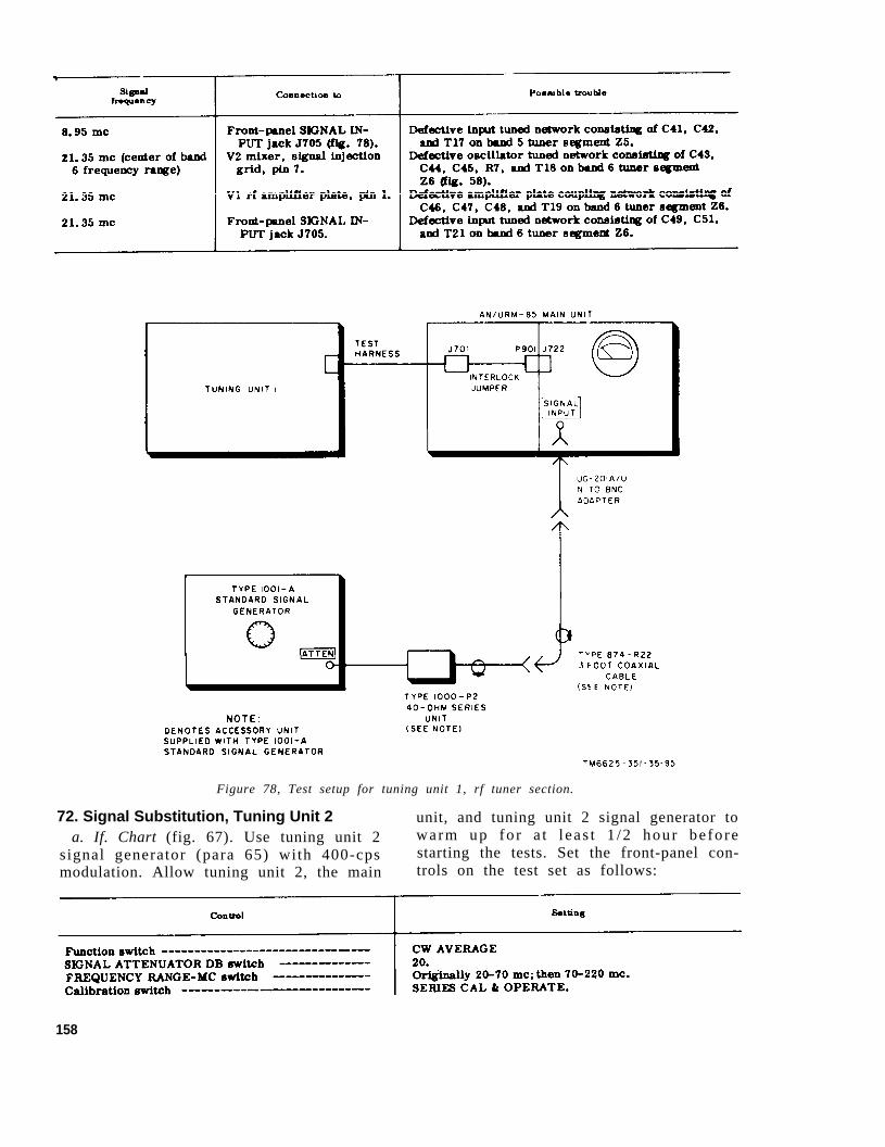
Figure 78, Test setup for tuning unit 1, rf tuner section.
72. Signal Substitution, Tuning Unit 2 unit, and tuning unit 2 signal generator toa. If. Chart (fig. 67). Use tuning unit 2 warm up fo r a t l eas t 1 /2 hour be fo re
signal generator (para 65) with 400-cps starting the tests. Set the front-panel con-modulation. Allow tuning unit 2, the main trols on the test set as follows:
158
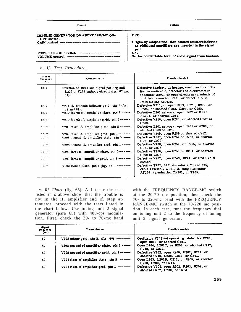
Figure 48.
Figure 67.
Figure 65.
Figure48.
b. If. Test Procedure.
c. Rf Chart (fig. 65). A f t e r the tests with the FREQUENCY RANGE-MC switchlisted in b above show that the trouble is at the 20-70 rnc position; then check thenot in the if . amplif ier and if . s tep at- 70- to 220-mc band with the FREQUENCYtenuator, proceed with the tests listed in RANGE-MC switch at the 70-220 mc posi-the chart below. Use tuning unit 2 signal tion. In each case, tune the frequency dialgenerator (para 65) with 400-cps modula- on tuning unit 2 to the frequency of tuningtion. First, check the 20- to 70-mc band unit 2 signal generator.
159
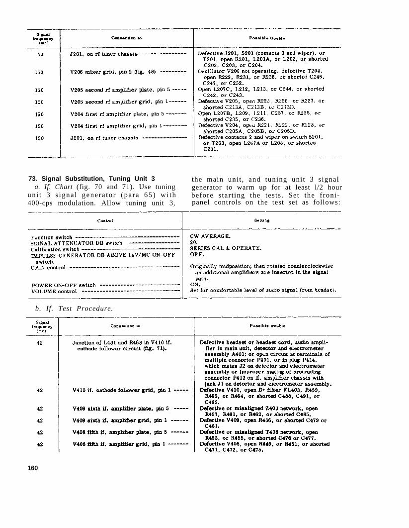
Figure 48.
Figure 71.
73. Signal Substitution, Tuning Unit 3 the main unit , and tuning unit 3 s ignala. If. Chart (fig. 70 and 71). Use tuning generator to warm up for at least l/2 hour
un i t 3 s igna l genera to r (pa ra 65) wi th before star t ing the tests . Set the froni-400-cps modulation. Allow tuning unit 3, panel controls on the test set as follows:
b. If. Test Procedure.
160
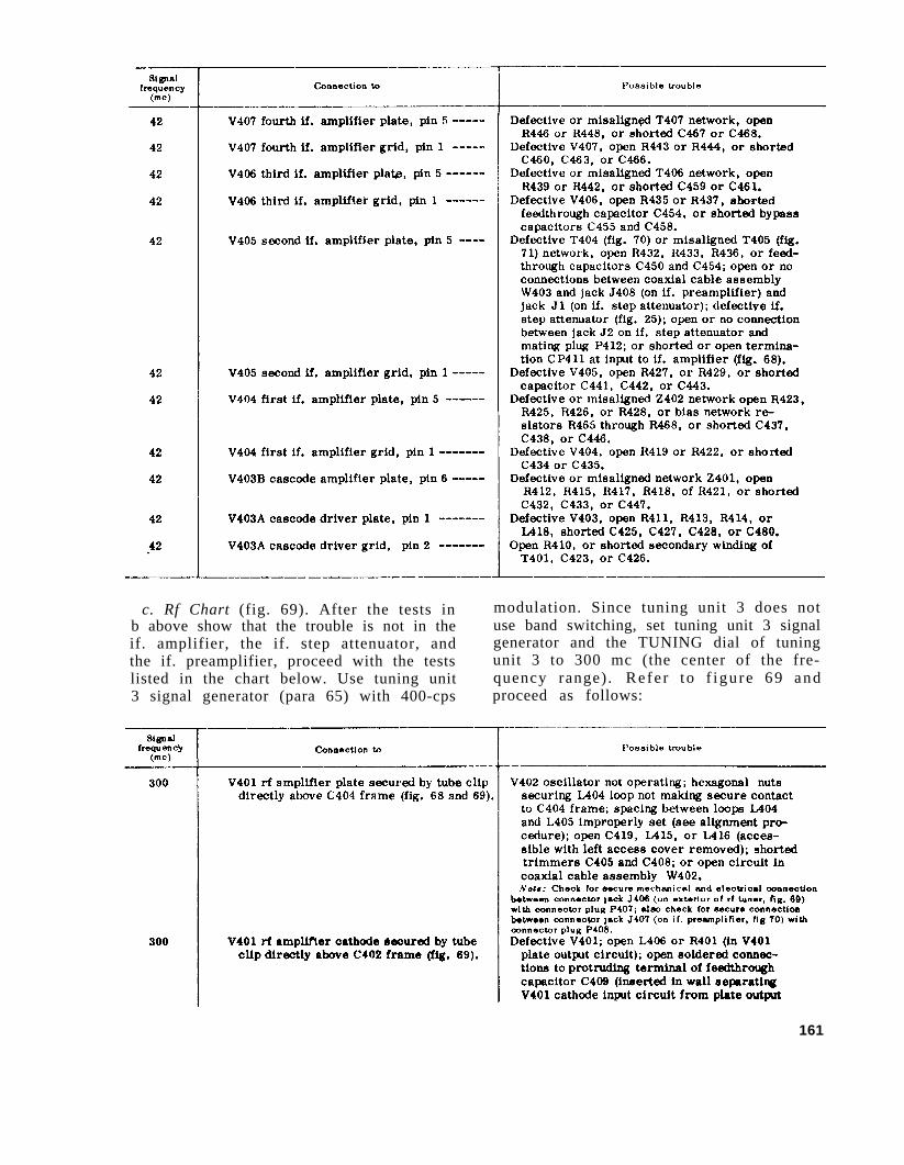
Figure 70.
Figure 25.
figure 68.
Figure 69.
Figure 70.
Figure 69.
Figure 68.
c. Rf Chart (fig. 69). After the tests in modulation. Since tuning unit 3 does notb above show that the trouble is not in the use band switching, set tuning unit 3 signalif. amplifier, the if. step attenuator, and generator and the TUNING dial of tuningthe if. preamplifier, proceed with the tests unit 3 to 300 mc (the center of the fre-listed in the chart below. Use tuning unit quency range). Refe r to f igure 69 and3 signal generator (para 65) with 400-cps proceed as follows:
161
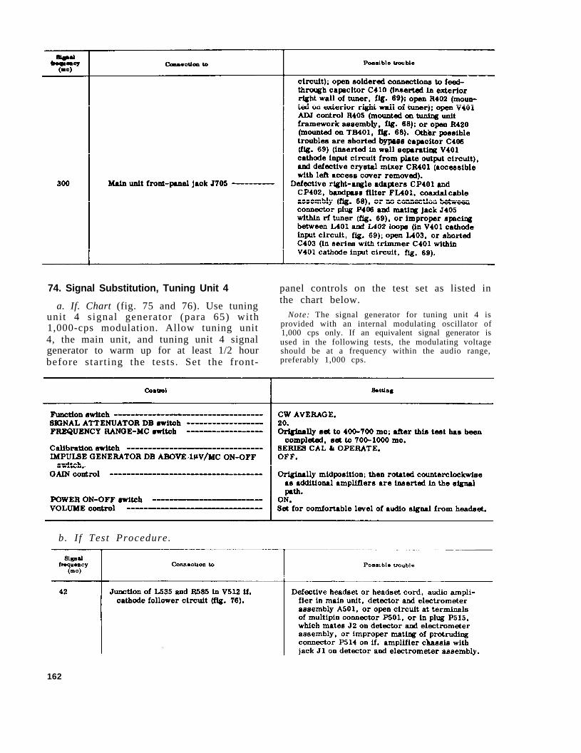
Figure 69.
Figure 68.
Figure 68.
Figure 69.
Figure 68.
Figure 69.
Figure 69.
Figure 69.
74. Signal Substitution, Tuning Unit 4 panel controls on the test set as listed in
a. If. Chart (fig. 75 and 76). Use tuningthe chart below.
unit 4 s ignal generator (para 65) with Note: The signal generator for tuning unit 4 is
1,000-cps modulation. Allow tuning unit provided with an internal modulating oscillator of
4, the main unit, and tuning unit 4 signal1,000 cps only. If an equivalent signal generator isused in the following tests, the modulating voltage
generator to warm up for at least 1/2 hour should be at a frequency within the audio range,before star t ing the tests . Set the front- preferably 1,000 cps.
b. I f Test Procedure.
162
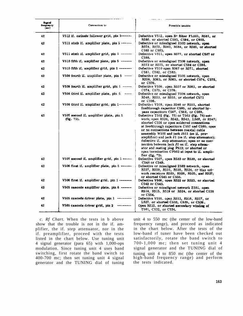
Figure 75.figure 76.
Figure 72.
c. Rf Chart. When the tests in b above unit 4 to 550 mc (the center of the low-bandshow that the trouble is not in the if. am-plifier, the if. step attenuator, nor in theif . preamplifier , proceed with the testslisted in the chart below. Use tuning unit4 signal generator (para 65) with 1,000-opsmodulation. Since tuning unit 4 uses bandswitching, first rotate the band switch to400-700 mc; then set tuning unit 4 signalgenerator and the TUNING dial of tuning
frequency range), and proceed as indicatedin the chart below. After the tests of thelow-band rf tuner have been checked outsat isfactori ly, rotate the band switch to700-1 ,000 mc ; then se t t un ing un i t 4signal generator and the TUNING dial oftuning unit 4 to 850 mc (the center of thehigh-band frequency range) and performthe tests indicated.
163
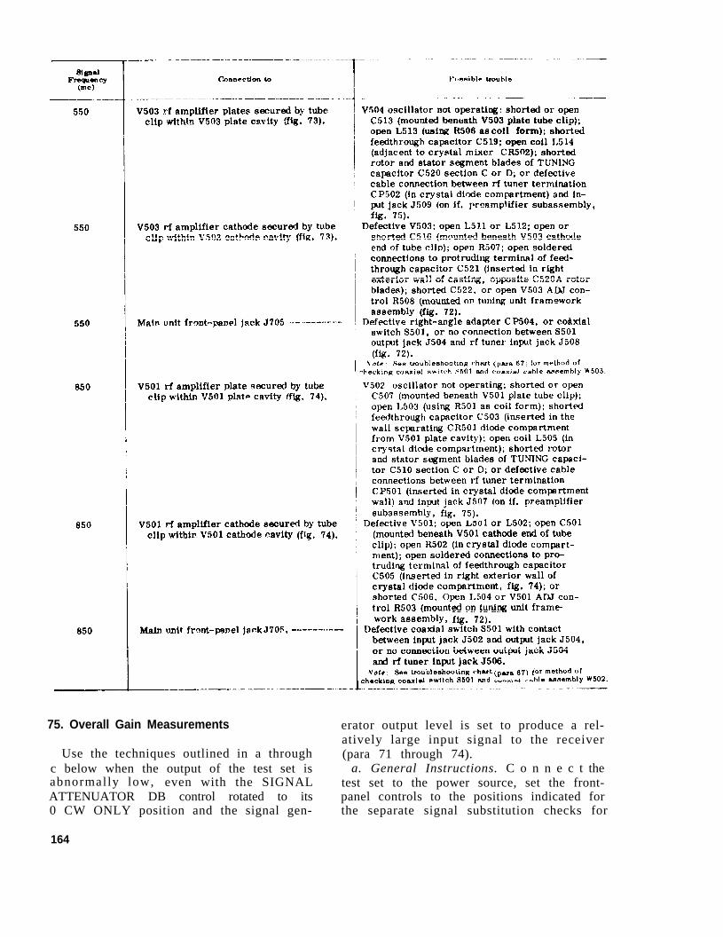
Figure 73.
Figure 73.
Figure 73.
Figure 72.
Figure 72
Para 67.
Figure 74.
Figure 75.
Figure 74.
Figure 72.
Para 67.
75. Overall Gain Measurements
Use the techniques outlined in a throughc below when the output of the test set isabnormally low, even with the SIGNALATTENUATOR DB control rotated to its0 CW ONLY position and the signal gen-
164
erator output level is set to produce a rel-atively large input signal to the receiver(para 71 through 74).
a. General Instructions. C o n n e c t thetest set to the power source, set the front-panel controls to the positions indicated forthe separate signal substitution checks for
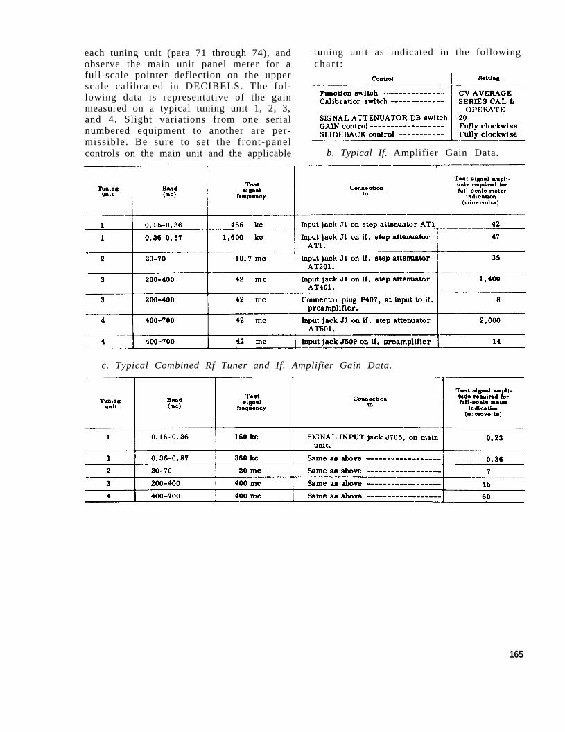
each tuning unit (para 71 through 74), andobserve the main unit panel meter for afull-scale pointer deflection on the upperscale calibrated in DECIBELS. The fol-lowing data is representative of the gainmeasured on a typical tuning unit 1, 2, 3,and 4. Slight variations from one serialnumbered equipment to another are per-missible. Be sure to set the front-panelcontrols on the main unit and the applicable
tuning unit as indicated in the followingchar t :
b. Typical If. Amplifier Gain Data.
c. Typical Combined Rf Tuner and If. Amplifier Gain Data.
165
Figure 80.
Figure 80.
CHAPTER 3
REPAIRS AND ALIGNMENT
Section I. REPAIRS
76. Replacement of Parts, MinorComponents for Use with TuningUnit 1
a. General. After completing the testsoutlined in paragraph 71, the signal sub-s t i t u t i o n t e c h n i q u e c a n b e u s e d f o rdetermining whether parts within the minorcomponents supplied for use with tuningu n i t 1 r e q u i r e r e p a i r o r r e p l a c e m e n t .These tests are performed with tuning unit1 installed in the tuning unit compartmentof the main unit. The following proceduresare based on the assumption that sourcesof trouble in both tuning unit 1 and the mainunit have been eliminated, and that thereis no need for operat ing tuning uni t 1 ,through the test harness, outside of themain unit. The following checks are to bemade with tuning unit 1 installed in the mainunit tuning unit compartment. In all tests,a cable assembly, consisting of a 3-footlength of RG-5B/U coaxial cable termi-nated by UG-18/U connectors, is used tocouple the test signal from the output ofthe minor component under test to the mainu n i t front-panel SIGNAL INPUT jack(J705). Set the front-panel controls aslisted in paragraph 71a, except for using
only band 1 of the MEGACYCLES switch(.15-.36) mc posit ion. Apply the signalthat is indicated in the signal frequencycolumn of the charts in b below. Monitorthe final output by observing an onscaleindication on the main unit panel meter. Ifnecessary, rotate the SIGNAL ATTENU-ATOR DB control to higher or lower stepsthan its initially recommended 20-db stepposition so that the relative amplitude ofthe test s ignal can be observed on themeter. A second method of monitoring thefinal output can be obtained by connectingthe headset, through the headset cord, intothe main unit front-panel PHONES jack.If the signal source is modulated at anaudio frequent y rate and an audio note isnot heard in the headset, trouble is indi-catid. Isolate the trouble as indicated inthe Possible t rouble and correct ion col-umn of the following charts, and repair orreplace the defective part or parts. Con-nect tuning unit 1 signal generator, m@-lated at 400 cps, to the test set as shownin figure 79, and follow the proceduresgiven in b below.
b. Coupler, Radio Frequency Interfer-ence CD-891/URM-85 (fig. 38 and 80).
166
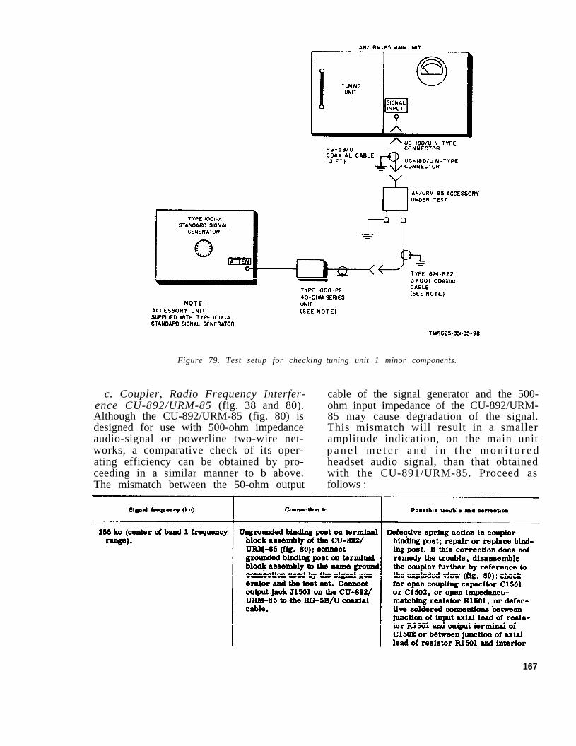
Figure 80.
Figure 80.
Figure 79. Test setup for checking
c. Coupler, Radio Frequency Interfer-ence CU-892/URM-85 (fig. 38 and 80).Although the CU-892/URM-85 (fig. 80) isdesigned for use with 500-ohm impedanceaudio-signal or powerline two-wire net-works, a comparative check of its oper-ating efficiency can be obtained by pro-ceeding in a similar manner to b above.The mismatch between the 50-ohm output
tuning unit 1 minor components.
cable of the signal generator and the 500-ohm input impedance of the CU-892/URM-85 may cause degradation of the signal.This mismatch will result in a smalleramplitude indication, on the main unitp a n e l m e t e r a n d i n t h e m o n i t o r e dheadset audio signal, than that obtainedwith the CU-891/URM-85. Proceed asfollows :
167
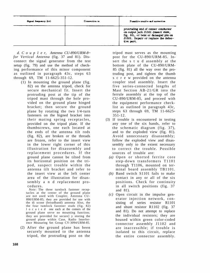
d. C o u p 1 e r, Antenna CU-890/URM-8~for Vertical Antenna (fig. 37 and 81). Dis-connect the signal generator from the testsetup (fig. 79) and use the method of check-ing performance of this minor componentas outl ined in paragraph 43c, s teps 63through 69, TM 11-6625-351-12.
(1) In mounting the ground plane (fig.
(2)
82) on the antenna tripod, check forsecure mechanical f i t . Insert theprotruding post at the tip of thetripod mast through the hole pro-vided on the ground plane hingedbracket; then secure the groundplane by rotating the two l/4-turnfasteners on the higned bracket intothe i r ma t ing sp r ing recep tac les ,provided on the tripod plate. If thethumbscrews, one each located atthe ends of the antenna tilt rods(fig. 82), are broken or the threadsare frozen, refer to the insert viewin the lower right corner of thisi l l u s t r a t ion fo r d i sa s sembly andr e p l a c e m e n t p r o c e d u r e s . I f t h eground plane cannot be tilted fromits horizontal position on the tri-pod , suspec t t roub le wi th in theantenna t i l t bracket and refer tothe insert view at the left centerarea of the illustration for disas-sembly a n d r ep lacement p ro -cedures .Note: The three turnlock fastener recep-
tacles at the center of the ground planeare not used with Coupler, Antenna CU-890/URM-85; they are provided for use withthe di scone (broadband) antenna Also, thethe four tumlock fastener studs (fig. 82)l o c a t e d one each at the comers of theground plane serve no mounting function;they are provided for secure] y storing theground plane within Case, Radio Interfer-ence Measuring Set Group CY-3094/URM-85.
After the ground plane has beensecurely mounted to the antennatripod, the protruding post on the
(3)
tripod mast serves as the mountingpost for the CU-890/URM-85. In-sert the s t u d assembly at thebottom plate of the CU-890/URM-85 (fig. 81) all the way over the pro-truding post, and tighten the thumbs c r e w provided on the antennacoupler stud assembly. Insert thefive series-connected lengths ofMast Section AB-21/GR into theferrule assembly at the top of theCU-890/URM-85, and proceed withthe equipment performance check-list as outlined in paragraph 43c,steps 63 through 69, TM 11-6625-351-12.If trouble is encountered in testingany one of the six bands, refer tothe schematic diagram (fig. 37),and to the exploded view (fig. 81).Avoid unnecessary disassembly;follow the exploded view and disas-sembly only to the extent necessaryto co r rec t the t roub le . Poss ib lesources of trouble are:
(a)
(b)
(c)
O p e n o r s h o r t e d f e r r i t e c o r es tep-down t rans fo rmers T1101through T1106, mounted on ter-minal board assembly TB1101.Band switch S1101 fails to makecontact in any or all of the sixposi t ions. Check for continui tyin all switch positions (fig. 37and 81).Open circuit in the impulse gen-e ra to r in jec t ion ne twork , con-sisting of series resistor R1101and shunt resistor R1102 (fig. 37and 81). Do not attempt to replacethe individual resistors; they arehoused within green color-codedconnector assembly J1102 andare inaccess ib le ; i f t roub le i sisolated to this circuit, replacethe entire connector assembly.
168
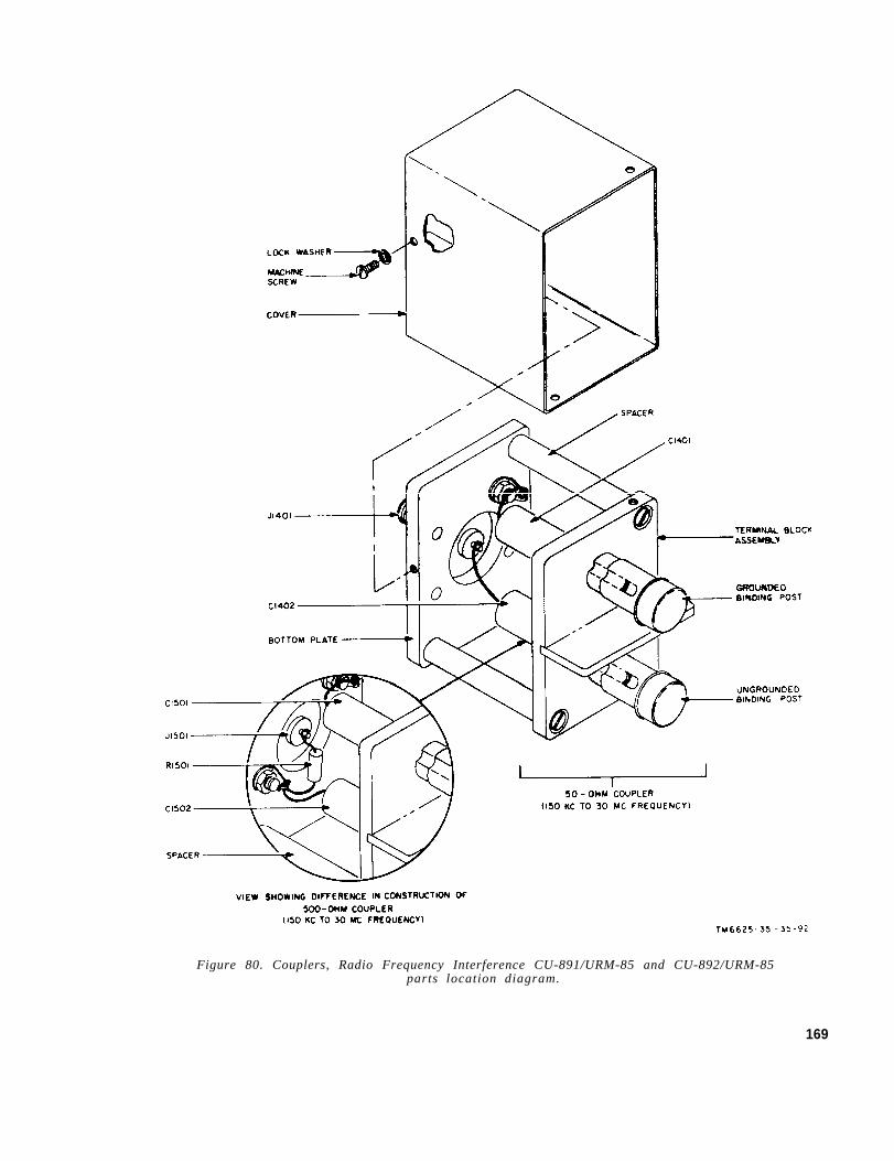
Figure 80. Couplers, Radio Frequency Interference CU-891/URM-85 and CU-892/URM-85parts location diagram.
169
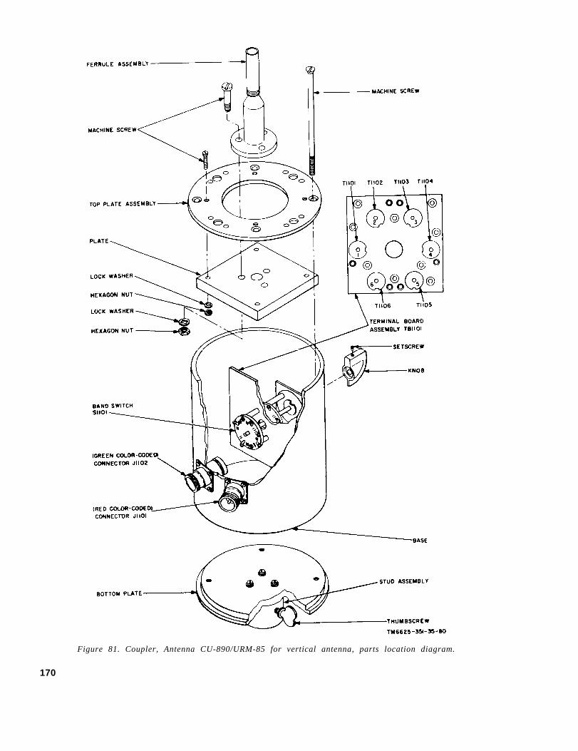
Figure 81. Coupler, Antenna CU-890/URM-85 for vertical antenna, parts location diagram.
170
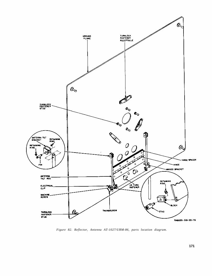
Figure 82. Reflector, Antenna AT-1027/URM-86, parts location diagram.
171
(d) Open or shorted circui t in thes i g n a l output red color-codedconnector J1101 (fig. 81). Checkfor continuity from the centerconductor to the wiper arm ofs w i t c h section S1101B. Alsocheck for infinite resistance be-tween the cen te r conduc to r o fJ1101 and the outer shell. If re-placement of J1101 is required,be sure to tag the lead connectedfrom S1101B wiper arm to Jll0l,before unsoldering, to facilitateproper rewiring.
e. Loop Antenna AT-l026/URM-85 (fig.83). Disconnect the signal generator fromthe test setup (fig. 79), and use the methodchecking performance of this minor com-ponent as outlined in paragraph 43b, steps70 through 72, TM 11-6625-351-12. If trou-ble is encountered in testing anyone of thesix bands, refer to the schematic diagram(fig. 36) and to the exploded view (fig. 83).Avoid unnecessary disassembly; follow theexploded view and disassemble only to theextent necessary to correct the trouble.Possible sources of trouble are:
(1)
(2)
(3)
(4)
Open or shorted ferrite core step-up t r ans fo rmers T1001 th roughT1004, mounted on terminal boardTB1001.Band switch S1001 fails to makecontact in any or al l of the s ixpositions. In bands 5 and 6 (fig.36), no coupling transformer isused. If trouble is encountered ineither of these bands, suspect faultycontacts 5 and 6, and the wiper onsection C of S1001.Open circuit in the impulse gen-erator injection network, consist-ing of series resis tor R1001 andshunt resistor R1002 (fig. 36). Donot attempt to replace the individualr e s i s t o r s , s ince they are housedand inaccessible w i t h i n greenco lo r -coded connec to r a s semblyJ1002; if trouble is isolated to thisc i r c u i t, replace the entire con-nector assembly.Open or shorted circuit in the sig-nal output red color-coded con-nector J1001. Check for continuity
from the center conductor to thew i p e r a r m o f s w i t c h s e c t i o nS1001B. Also check for infinite re-sistance between the center con-ductor of J1001 and the outer shell.I f r ep lacement o f J1001 i s r e -qu i red , be su re to t ag the l eadconnected from S1001B wiper armto J1001, before unsoldering, tofacilitate proper rewiring.
77. Replacement of Parts, MinorComponents for Use with TuningUnits 2, 3, and 4
a. General. After completing the testsoutlined in paragraphs 72 through 74, thesignal substitution technique can be usedfor determining whether parts within theminor components supplied for use withtuning units 2, 3, and 4 require repair orreplacement. These tests are performedwith the applicable tuning unit installed inthe tuning unit compartment of the mainunit. Similar to the procedure outlined inparagraph 7 la, the following proceduresare based on the assumption that sourcesof trouble in the installed tuning unit andthe main unit- have been eliminated. Alltests use Cable Assembly Set, ElectricalMX-3410/URM-85 as the means of couplingthe test signal from the output of the minorcomponent under test to front-panel SIGNAL INPUT jack (J705). It is only neces-sary to test the performance of the minorcomponent with either tuning unit 2, 3, or4 installed in the main unit. For conven-ience, the 20- to 70-mc band of tuning unit2 is used throughout the following pro-cedures. Set the front-panel controls aslisted in paragraph 72a; monitor the outputsignal by observing the pointer deflectionon the main unit panel meter. If desired,simultaneously monitor the modulated testsignal with the headset. Use tuning unit 4signal generator as the signal source, with1,000-cps modulation, and proceed as in-dicated in b below.
b. Coupler, Radio Frequency Interfer-ence CU-897/URM-85 (fig. 38 and 84). Inthe test setup of figure 79, replace tuningunit 1 signal generator with tuning unit 4signal generator. Use an alligator clip to
172
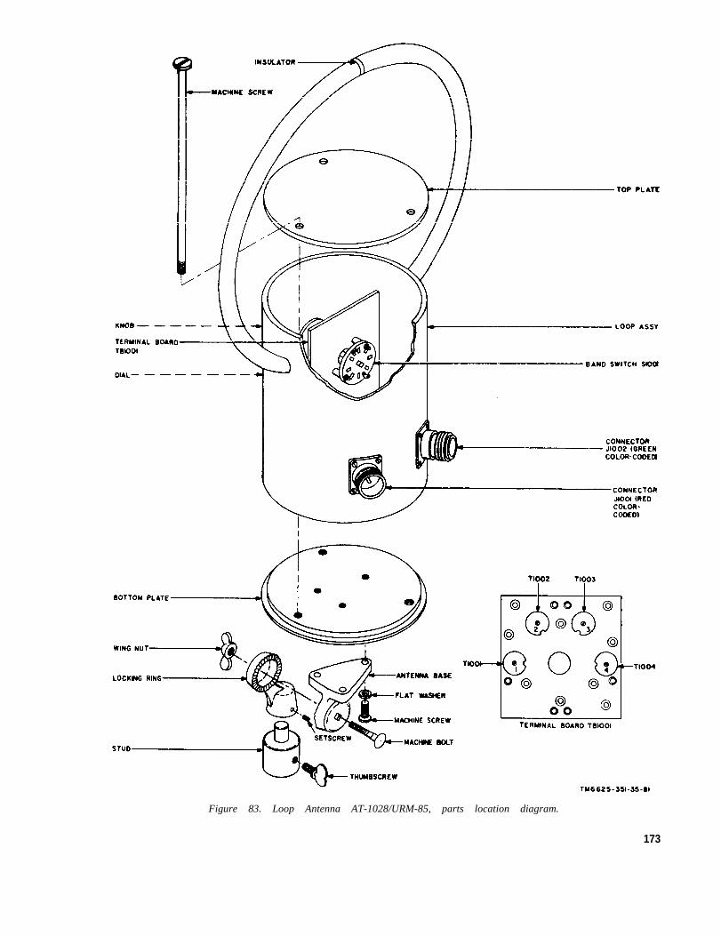
Figure 83. Loop Antenna AT-1028/URM-85, parts location diagram.
173
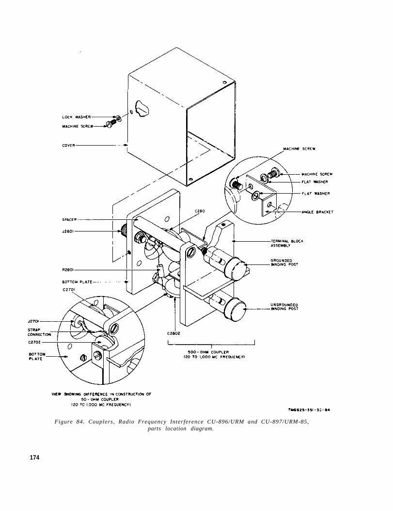
Figure 84. Couplers, Radio Frequency Interference CU-896/URM and CU-897/URM-85,parts location diagram.
174
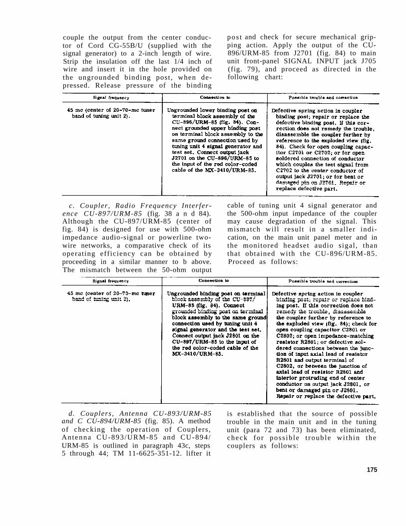
Figure 84.
Figure 84.
Figure 84.
Figure 84.
couple the output from the center conduc- pos ttor of Cord CG-55B/U (supplied with the ping
and check for secure mechanical grip-action. Apply the output of the CU-
signal generator) to a 2-inch length of wire. 896/URM-85 from J2701 (fig. 84) to mainStrip the insulation off the last 1/4 inch of unit front-panel SIGNAL INPUT jack J705wire and insert it in the hole provided on (fig. 79), and proceed as directed in thethe ungrounded binding post , when de- following chart:pressed. Release pressure of the binding
c. Coupler, Radio Frequency Interfer- cable of tuning unit 4 signal generator andence CU-897/URM-85 (fig. 38 a n d 84). the 500-ohm input impedance of the couplerAlthough the CU-897/URM-85 (center of may cause degradation of the signal. Thisfig. 84) is designed for use with 500-ohm mismatch wil l result in a smaller indi-impedance audio-signal or powerline two- cation, on the main unit panel meter and inwire networks, a comparative check of its the monitored headset audio sigal , thanoperat ing eff iciency can be obtained by that obtained with the CU-896/URM-85.proceeding in a similar manner to b above. Proceed as follows:The mismatch between the 50-ohm output
d. Couplers, Antenna CU-893/URM-85 is established that the source of possibleand C CU-894/URM-85 (fig. 85). A method trouble in the main unit and in the tuningof checking the operat ion of Couplers , unit (para 72 and 73) has been eliminated,Antenna CU-893/URM-85 and CU-894/ check fo r poss ib le t roub le wi th in theURM-85 is outlined in paragraph 43c, steps couplers as follows:5 through 44; TM 11-6625-351-12. lifter it
175
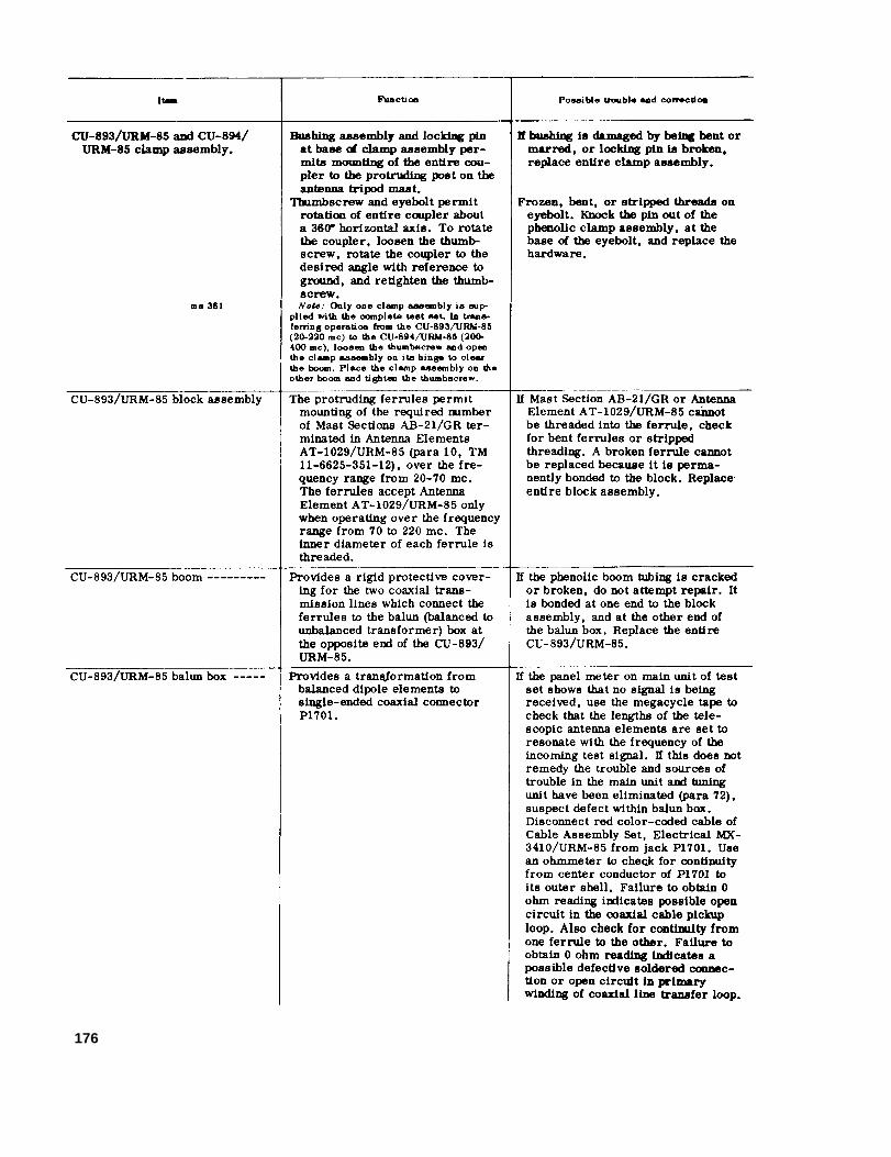
figure 72.
176
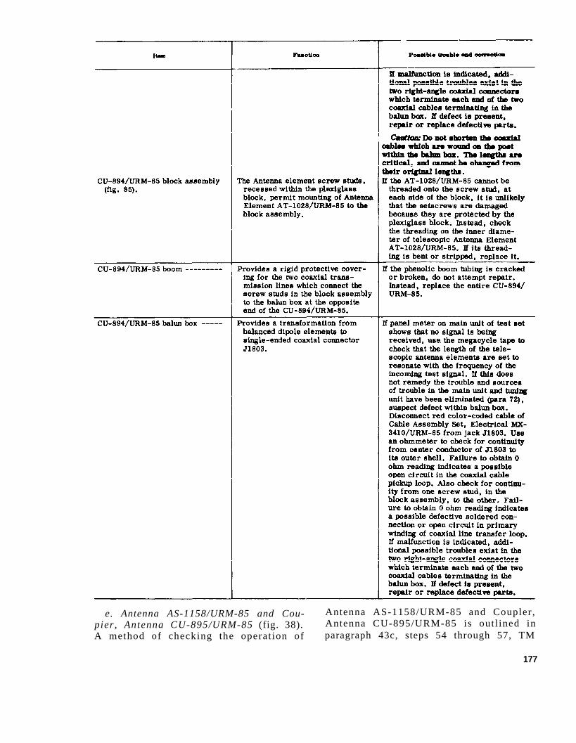
para 72.
e. Antenna AS-1158/URM-85 and Cou- Antenna AS-1158/URM-85 and Coupler ,pier, Antenna CU-895/URM-85 (fig. 38). Antenna CU-895/URM-85 is outl ined inA method of checking the operat ion of paragraph 43c, steps 54 through 57, TM
177
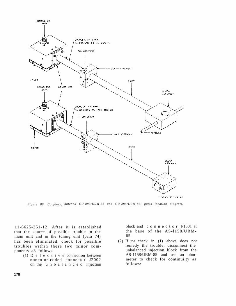
Figure 86. Couplers, Antenna CU-893/URM-86 and CU-894/URM-85, parts location diagram.
11-6625-351-12. After i t is establ ishedthat the source of possible trouble in themain unit and in the tuning unit (para 74)has been el iminated, check for possiblet roub les wi th in these two minor com-ponents a8 follows:
(1) D e f e c t i v e connection betweennoncolor-coded connector J2002on the u n b a l a n c e d injection
block and c o n n e c t o r P1601 atthe base o f the AS- l158 /URM-85.
(2) If the check in (1) above does notremedy the trouble, disconnect theunbalanced injection block from theAS-1158/URM-85 and use an ohm-meter to check for continui,ty asfollows:
178
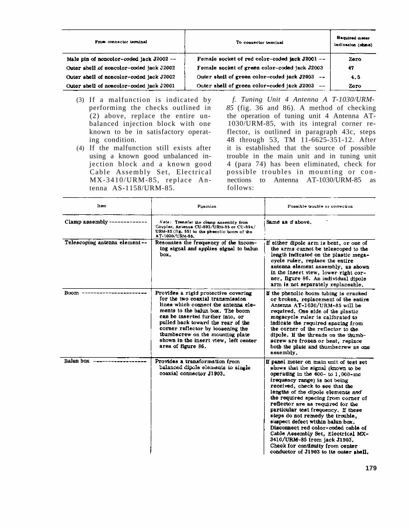
Fibure 86.
Figure 85.
(3)
(4)
If a malfunction is indicated byperforming the checks outlined in(2) above, replace the entire un-balanced injection block with oneknown to be in satisfactory operat-ing condition.If the malfunction still exists afterusing a known good unbalanced in-ject ion block and a known goodCable Assembly Se t , E lec t r i ca lMX-3410/URM-85 , rep lace An-
f. Tuning Unit 4 Antenna A T-1030/URM-85 (fig. 36 and 86). A method of checkingthe operation of tuning unit 4 Antenna AT-1030/URM-85, with its integral corner re-flector, is outlined in paragraph 43c, steps48 through 53, TM 11-6625-351-12. Afterit is established that the source of possibletrouble in the main unit and in tuning unit4 (para 74) has been eliminated, check forposs ib l e t roub le s in moun t ing o r con-nections to Antenna AT-1030/URM-85 as
tenna AS-1158/URM-85. follows:
179
78. Replacement of Parts, MinorComponents-for Use with AllTuning Units
a. Mul t imeter , Remote ME-204/URM-85 (fig. 87). During operation or checkingof the test set, the remote meter may beinterconnected to the main unit by usingCord Assembly , E lec t r i ca l CX-4305/U.One telephone plug PJ-068, at one end ofthe CX-4305/U, mates wi th main un i tf rent-panel jack J704; the second telephoneplug PJ-068, at the opposite end of the 30-foot cord, mates with telephone jack J1201on the remote meter. With this intercon-nection completed, the pointer on the re-mote meter should duplicate the indicationson the main unit panel meter. If malfunc-tioning of the remote meter is indicatedafter possible defects in the main unit havebeen eliminated (para 67), suspect a de-fec t ive co rd , t e l ephone j ack J1201 , o rmicroammeter M1201. Follow the explodedview (f ig. 87) for disassembly and re-assembly of replacement parts..
b. Cable Assembly, Special Purpose,Electrical B r a n c h e d CX-6681/URM-85(fig. 88). This cable assembly is used forinterconnecting a tuning unit, when opera-ting outside of the main unit for trouble-shooting (para 67) or signal substitution
180
(para 71-74), to the main unit. A typicaltest setup is shown in figure 46; the sche-matic diagram of the cable assembly isshown in figure 39. Other than open circuitsthat may develop in the soldered con-nections to plugs P902 and P903, possiblesources of trouble may exist as follows:
(1)
(2)
Failure of contact closure withinm i c r o s w i t c h S901, which ismounted to the bellhousing on con-nector P902. The contact shouldclose when connector P902 is in-serted as far as possible into itsmating receptacle at the rear of atuning unit. Failure to hear a click-ing sound, when inserting the con-nector into the receptacle, is causefor suspecting a defective micro-switch. D i s a s s e m b l y and re-assembly is accomplished by thetwo screws that secure the micro-switch to the bellhousing.
Failure of contact closure withinm i c r o s w i t c h S902, which ismounted to the bellhousing on con-nector P903. The contact shouldclose when connector P903 is in-serted as far as possible into itsmating receptacle J701 on the in-terior wall of the main unit tuning
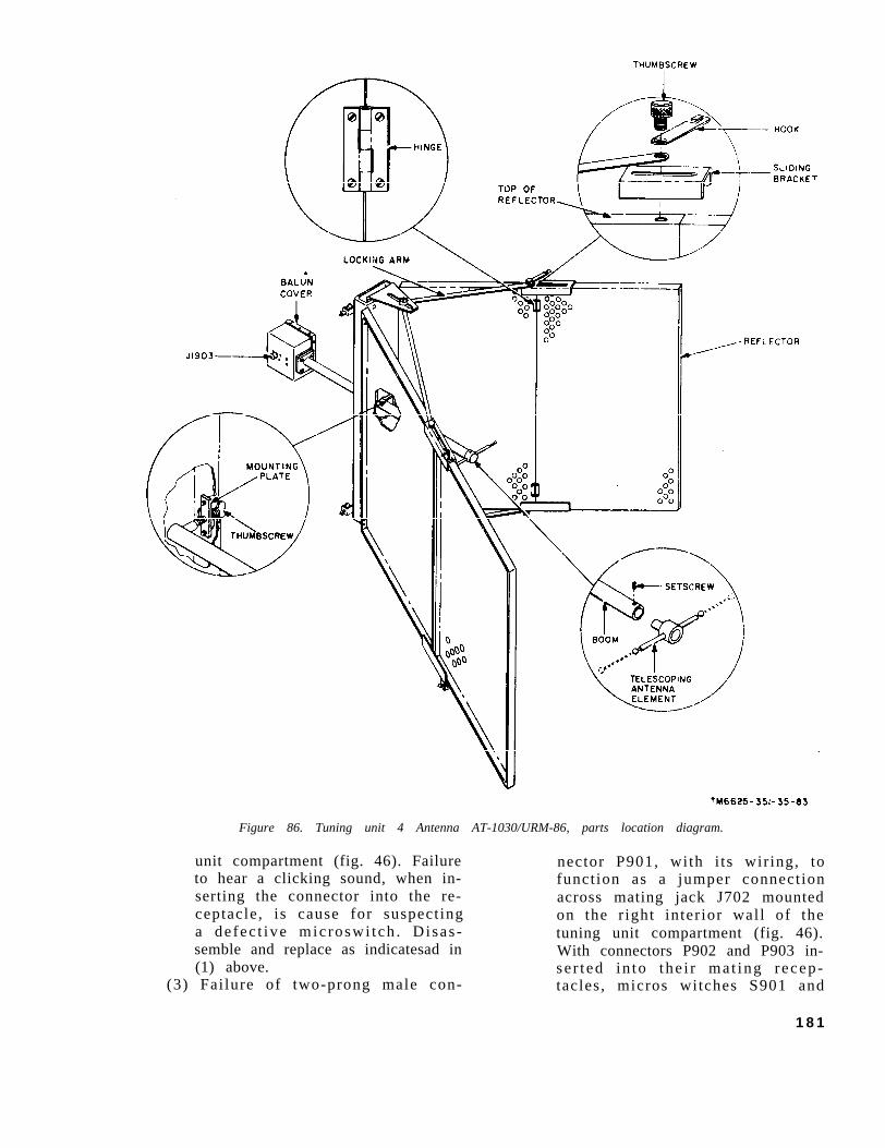
Figure 86. Tuning unit 4 Antenna AT-1030/URM-86, parts location diagram.
unit compartment (fig. 46). Failureto hear a clicking sound, when in-serting the connector into the re-ceptacle, is cause for suspectinga de fec t ive mic roswi tch . Disas -semble and replace as indicatesad in(1) above.
(3) Failure of two-prong male con-
nector P901, with i ts wiring, tofunction as a jumper connectionacross mating jack J702 mountedon the r ight inter ior wall of thetuning unit compartment (fig. 46).With connectors P902 and P903 in-se r t ed in to the i r ma t ing recep-tacles, micros witches S901 and
1 8 1
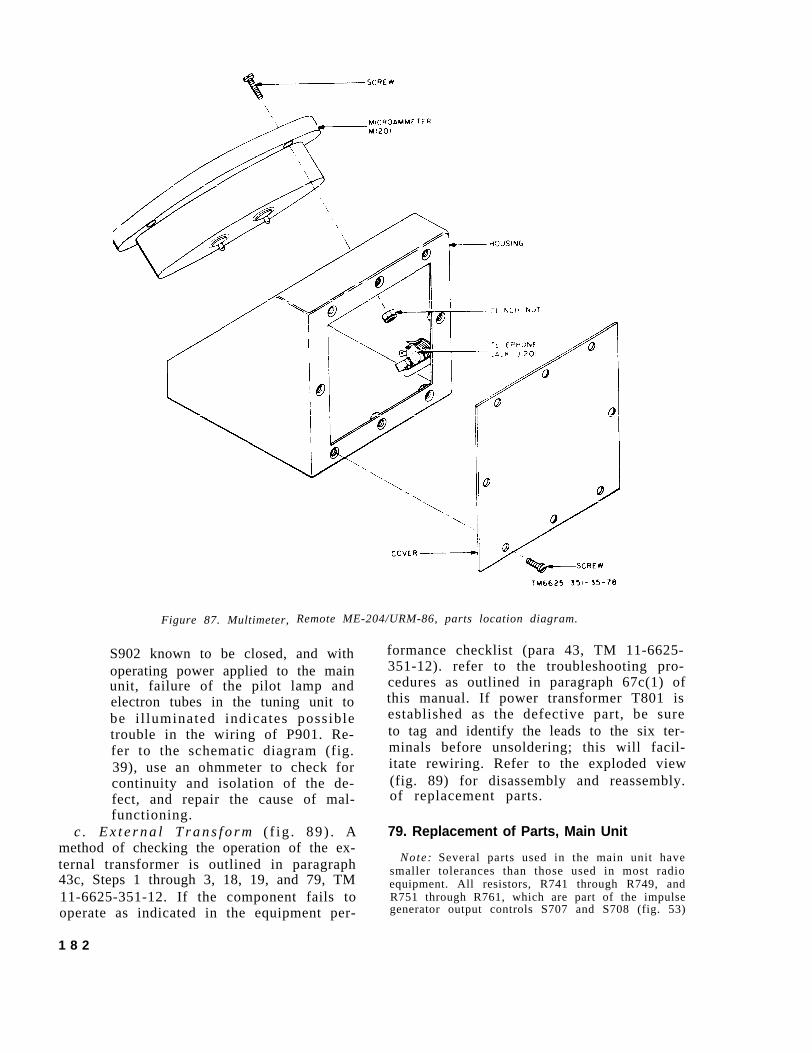
Figure 87. Multimeter, Remote ME-204/URM-86, parts location diagram.
S902 known to be closed, and withoperating power applied to the mainunit, failure of the pilot lamp andelectron tubes in the tuning unit tobe i l luminated indicates possibletrouble in the wiring of P901. Re-fer to the schematic diagram (fig.39), use an ohmmeter to check forcontinuity and isolation of the de-fect, and repair the cause of mal-functioning.
c . E x t e r n a l T r a n s f o r m ( f ig . 89) . Amethod of checking the operation of the ex-ternal transformer is outlined in paragraph43c, Steps 1 through 3, 18, 19, and 79, TM11-6625-351-12. If the component fails tooperate as indicated in the equipment per-
1 8 2
formance checklist (para 43, TM 11-6625-351-12). refer to the troubleshooting pro-cedures as outlined in paragraph 67c(1) ofthis manual. If power transformer T801 isestablished as the defective part, be sureto tag and identify the leads to the six ter-minals before unsoldering; this will facil-itate rewiring. Refer to the exploded view(fig. 89) for disassembly and reassembly.of replacement parts.
79. Replacement of Parts, Main Unit
Note: Several parts used in the main unit havesmaller tolerances than those used in most radioequipment. All resistors, R741 through R749, andR751 through R761, which are part of the impulsegenerator output controls S707 and S708 (fig. 53)
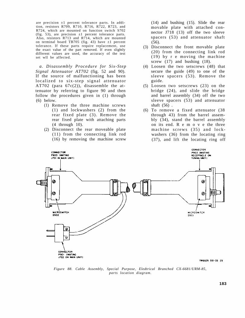
are precision ±1 percent tolerance parts. In addi-tion, resistors R709, R710, R716, R722, R723, andR724, which are mounted on function switch S702(fig. 53), are precision ±1 percent tolerance parts.Also, resistors R713 and R714, which are mountedon terminal board TB705 (fig. 43) have ±1 percenttolerance. If these parts require replacement, usethe exact value of the part removed. If even slightlydifferent values are used, the accuracy of the testset wll be affected.
a. Disassembly Procedure for Six-StepSignal Attenuator AT702 (fig. 52 and 90).If the source of malfunctioning has beenloca l i zed to s ix - s t ep s igna l a t t enua to rAT702 (para 67c(2)), disassemble the at-tenuator by referring to figure 90 and thenfollow the procedures given in (1) through(6) below.
(1)
(2)
Remove the three machine screws(1) and lockwashers (2) from therear f ixed plate (3) . Remove therear fixed plate with attaching parts(4 through 10).Disconnect the rear moveable plate(11) from the connecting link rod(16) by removing the machine screw
(3)
(4)
(5)
(6)
(14) and bushing (15). Slide the rearmovable plate with attached con-nector J718 (13) off the two sleevespacers (53) and attenuator shaft(56).Disconnect the front movable plate(20) from the connecting link rod(19) by r e moving the machinescrew (17) and bushing (18).Loosen the two setscrews (48) thatsecure the guide (49) to one of thesleeve spacers (53). Remove theguide.Loosen two setscrews (23) on thebridge (24), and slide the bridgeand barrel assembly (34) off the twosleeve spacers (53) and attenuatorshaft (56) .To remove a fixed attenuator (38through 43) from the barrel assem-bly (34), stand the barrel assemblyon its end. R e m o v e the threemach ine sc rews (35) and lock-washers (36) from the locating ring(37), and lift the locating ring off
Figure 88. Cable Assembly, Special Purpose, Eledtrical Branched CX-6681/URM-85,parts location diagram.
183
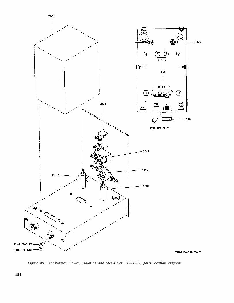
Figure 89. Transformer. Power, Isolation and Step-Down TF-248/G, parts location diagram.
184
the barrel assembly. Twist the de-fective fixed attenuator to free itstwo lugs from the grooves in theconnecting tube (44).
Caution: Fixed attenuator valuesare marked on the rear locatingring (47). Bc sure to replace thefixed attenuator in their properlocations. When replacing eitherlocating ring (37 or 47), make surethat the flats in the center hole ofeach locating ring align. The threemachine screws (35 or 45) will thenline up with the mating holes on theconnecting tube (44).
b. Reassembly Procedure for Six-StepSignal
(1)
(2)
(3)
(4)
(5)
(6)
(7)
(8)
Attenuator AT702 (fig. 90).Working from the rear of the at-tenuator, assemble the barrel as-sembly (34). Position the assemblyso that the markings on the rearlocating ring (47) face the repair-man .Place the assembled bridge (24)against the barrel assembly (34).Orient the spring (32) and roller(33) as shown in figure 90.Slide the bridge and barrel assem-b ly toge the r on the two s l eevespacers (53) and attenuator shaft(56), respectively; orient them asshown in figure 90. Do not tightenthe setscrews (23) at this point .Connect the front movable plate(20) to the connecting link rod (19);use the machine screw (17) andbushing (18).Slide the guide (49) on the thirds leeve space r (53) a s shown infigure 90. The thicker ridge of theguide should face the front of theattenuator. Do not tighten the set-screw (48) at this point of reas-sembly.Engage the rear locating ring (47)with the groove of the guide (49).Install the rear movable plate (11)on the attenuator shaft (56) and thetwo sleeve spacers (53) that engagethe bridge (24).Connect the rear movable plate (11)to the connecting link rod (16); use
(9)
(10)
(11)
(12)
the machine screw (14) and bushing(15).Instal l the assembled rear f ixedfixed plate (3) so that its notchedgroove accommoda tes connec to rJ718 (13). Tighten the rear fixedplate (3) to the sleeve spacers (53)with the three machine screws (1)and lockwashers (2).Pull the front and rear movableplates (11 and 20) against the frontand rear fixed plates (3 and 52).Hold the plates in this position, andtighten the two setscrews (23) thatsecure the bridge (24) to the sleevespacers (53).P u s h t h e a s s e m b l e d a t t e n u a t o rclosed. Now tighten the two set-screws (48) that secure the guide(49) to the sleeve spacer. Be sureto engage the groove of the guidewith the rear locat ing r ing (47).Check fo r smooth r id ing ac t ionwithout binding.Hold the a s s e m b 1 e d attenuatorclosed, and orient the roller (33)so that it makes contact simulta-neously with two of the fixed at-tenuators (38) through 43). Tightenthe screw (30), and check to seethat the roller is properly centered.
c. Replacement of Fixed20-DB Attenua-tor AT701 (fig. 51-52). Fixed 20-db at-tenuator AT701 is in series with the outputof inpulse generator G701 (fig. 51) onlywhen the front-panel calibration switch isin the SHUNT CAL position. A convenientmethod of checking the operation of fixed20-db attenuator AT701 is to set the IM-PULSE GENERATOR DB ABOVE 1µV/MC ON-OFF switch ON and to set the cali-bration switch to the SHUNT CAL position.Set the impulse generator coarse and fineoutput controls to a high setting, such as80. If the panel meter on the test set showsa pointer deflection, this is an indicationthat the impulse generator is producingan output calibrating signal; then connectone of the series-calibrated antennas (suchas the loop, vertical, or discone antenna,depending on the tuning unit used) to theIMPULSE OUTPUT jack on the main unitfront panel . Use the green color-coded
185
Figure 90. Six-step signal attenuator AT702, parts location diagram.
186
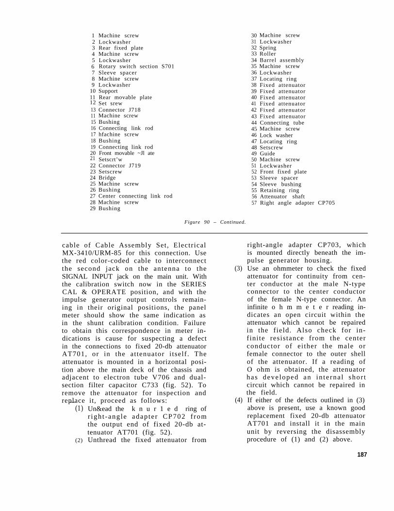
123456789
1011121311151617181920212223242526272829
Machine screwLockwasherRear fixed plateMachine screwLockwasherRotary switch section S701Sleeve spacerMachine screwLockwasherSupportRear movable plateSet srewConnector J718Machine screwBushingConnecting link rodhfachine screwBushingConnecting link rodFront movable ~Jl ateSetscrt’wConnector J719SetscrewBridgeMachine screwBushingCenter connecting link rodMachine screwBushing
Figure 90 – Continued.
30313233343536373839404142434445464748495051525354555657
Machine screwLockwasherSpringRollerBarrel assemblyMachine screwLockwasherLocating ringFixed attenuatorFixed attenuatorFixed attenuatorFixed attenuatorFixed attenuatorFixed attenuatorConnecting tubeMachine screwLock washerLocating ringSetscrewGuideMachine screwLockwasherFront fixed plateSleeve spacerSleeve bushingRetaining ringAttenuator shaftRight angle adapter CP705
cable of Cable Assembly Set, ElectricalMX-3410/URM-85 for this connection. Usethe red color-coded cable to interconnectthe second jack on the antenna to the (3)SIGNAL INPUT jack on the main unit. Withthe calibration switch now in the SERIESCAL & OPERATE position, and with theimpulse generator output controls remain-ing in their original positions, the panelmeter should show the same indication asin the shunt calibration condition. Failureto obtain this correspondence in meter in-dications is cause for suspecting a defectin the connections to fixed 20-db attenuatorAT701, or in the at tenuator i tself . Theattenuator is mounted in a horizontal posi-tion above the main deck of the chassis andadjacent to electron tube V706 and dual-section filter capacitor C733 (fig. 52). Toremove the attenuator for inspection andreplace it, proceed as follows: (4)—
(1)
(2)
Un&ead the k n u r 1 e d ring ofr igh t -ang le adap te r CP702 f romthe output end of fixed 20-db at-tenuator AT701 (fig. 52).Unthread the fixed attenuator from
right-angle adapter CP703, whichis mounted directly beneath the im-pulse generator housing.Use an ohmmeter to check the fixedattenuator for continuity from cen-ter conductor at the male N-typeconnector to the center conductorof the female N-type connector. Aninfinite o h m m e t e r reading in-dicates an open circuit within theattenuator which cannot be repairedin the f ield. Also check for in-f ini te resistance from the centerconductor of ei ther the male orfemale connector to the outer shellof the attenuator. If a reading ofO ohm is obtained, the attenuatorhas deve loped an in t e rna l shor tcircuit which cannot be repaired inthe field.If either of the defects outlined in (3)above is present, use a known goodreplacement fixed 20-db attenuatorAT701 and install it in the mainunit by reversing the disassemblyprocedure of (1) and (2) above.
187
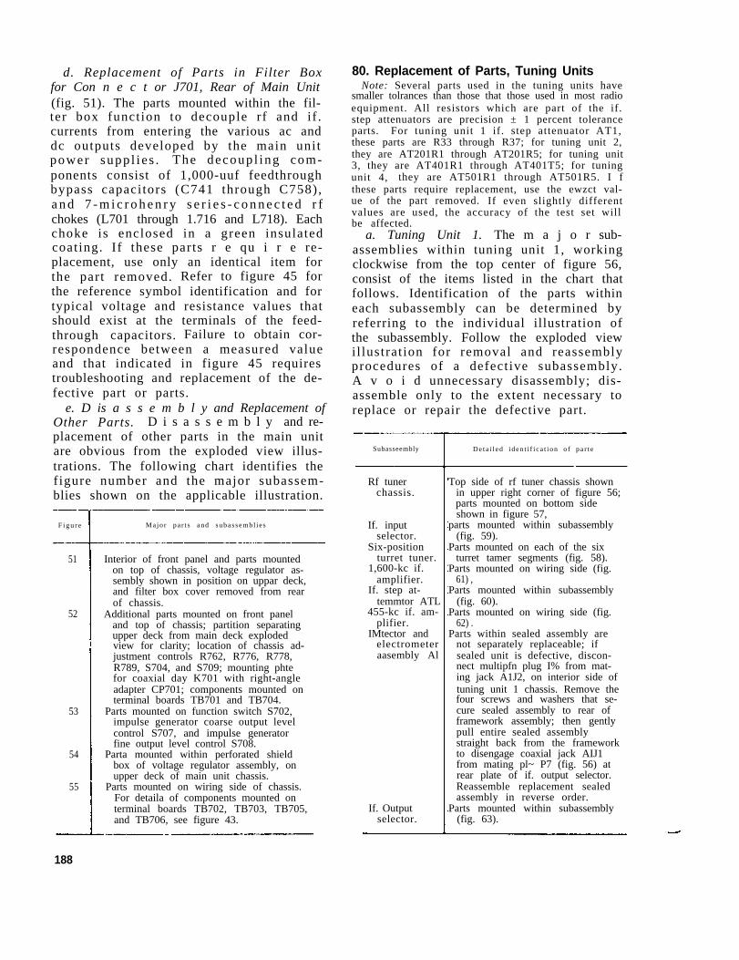
d. Replacement of Parts in Filter Boxfor Con n e c t or J701, Rear of Main Unit(fig. 51). The parts mounted within the fil-ter box function to decouple rf and if .currents from entering the various ac anddc outputs developed by the main unitpower supp l i e s . The decoup l ing com-ponents consist of 1,000-uuf feedthroughbypass capaci tors (C741 through C758),a n d 7 - m i c r o h e n r y s e r i e s - c o n n e c t e d r fchokes (L701 through 1.716 and L718). Eachchoke is enclosed in a green insulatedcoating. If these parts r e qu i r e re-placement, use only an identical item forthe part removed. Refer to figure 45 forthe reference symbol identification and fortypical voltage and resistance values thatshould exist at the terminals of the feed-through capacitors. Failure to obtain cor-respondence between a measured valueand that indicated in figure 45 requirestroubleshooting and replacement of the de-fective part or parts.
e. D is a s s e m b l y and Replacement ofOther Parts. D i s a s s e m b l y and re-placement of other parts in the main unitare obvious from the exploded view illus-trations. The following chart identifies thefigure number and the major subassem-blies shown on the applicable illustration.
F i g u r e
51
52
53
54
55
188
Majo r pa r t s and subas sembl i e s
Interior of front panel and parts mountedon top of chassis, voltage regulator as-sembly shown in position on uppar deck,and filter box cover removed from rearof chassis.
Additional parts mounted on front paneland top of chassis; partition separatingupper deck from main deck explodedview for clarity; location of chassis ad-justment controls R762, R776, R778,R789, S704, and S709; mounting phtefor coaxial day K701 with right-angleadapter CP701; components mounted onterminal boards TB701 and TB704.
Parts mounted on function switch S702,impulse generator coarse output levelcontrol S707, and impulse generatorfine output level control S708.
Parta mounted within perforated shieldbox of voltage regulator assembly, onupper deck of main unit chassis.
Parts mounted on wiring side of chassis.For detaila of components mounted onterminal boards TB702, TB703, TB705,and TB706, see figure 43.
80. Replacement of Parts, Tuning UnitsNote: Several parts used in the tuning units have
smaller tolrances than those that those used in most radioequipment. All resistors which are part of the if.step attenuators are precision ± 1 percent toleranceparts. For tuning unit 1 if. step attenuator AT1,these parts are R33 through R37; for tuning unit 2,they are AT201R1 through AT201R5; for tuning unit3, they are AT401R1 through AT401T5; for tuningunit 4, they are AT501R1 through AT501R5. I fthese parts require replacement, use the ewzct val-ue of the part removed. If even slightly differentvalues are used, the accuracy of the test set willbe affected.
a. Tuning Unit 1. The m a j o r sub-assemblies within tuning unit 1, workingclockwise from the top center of figure 56,consist of the items listed in the chart thatfollows. Identification of the parts withineach subassembly can be determined byreferring to the individual illustration ofthe subassembly. Follow the exploded viewil lustrat ion for removal and reassemblyprocedures of a defect ive subassembly.A v o i d unnecessary disassembly; dis-assemble only to the extent necessary toreplace or repair the defective part.
Subasseembly
Rf tunerchassis.
If. inputselector.
Six-positionturret tuner.
1,600-kc if.amplifier.
If. step at-temmtor ATL
455-kc if. am-plifier.
IMtector andelectrometeraasembly Al
If. Outputselector.
D e t a i l e d i d e n t i f i c a t i o n o f p a r t e
Top side of rf tuner chassis shownin upper right corner of figure 56;parts mounted on bottom sideshown in figure 57,
parts mounted within subassembly(fig. 59).
Parts mounted on each of the sixturret tamer segments (fig. 58).
Parts mounted on wiring side (fig.61) ,
Parts mounted within subassembly(fig. 60).
Parts mounted on wiring side (fig.62) .
Parts within sealed assembly arenot separately replaceable; ifsealed unit is defective, discon-nect multipfn plug I% from mat-ing jack A1J2, on interior side oftuning unit 1 chassis. Remove thefour screws and washers that se-cure sealed assembly to rear offramework assembly; then gentlypull entire sealed assemblystraight back from the frameworkto disengage coaxial jack AIJ1from mating pl~ P7 (fig. 56) atrear plate of if. output selector.Reassemble replacement sealedassembly in reverse order.
Parts mounted within subassembly(fig. 63).
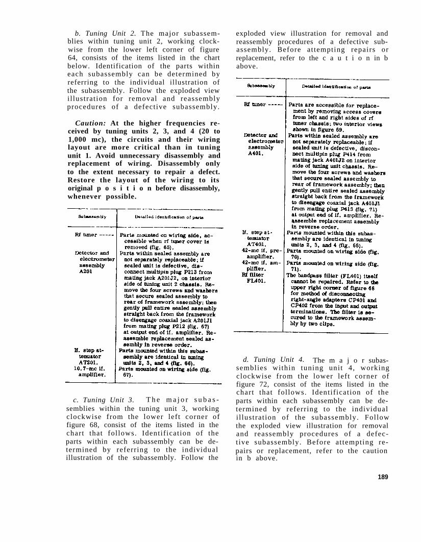
b. Tuning Unit 2. The major subassem-blies within tuning unit 2, working clock-wise from the lower left corner of figure64, consists of the items listed in the chartbelow. Identification of the parts withineach subassembly can be determined byreferring to the individual illustration ofthe subassembly. Follow the exploded viewil lustrat ion for removal and reassemblyprocedures of a defect ive subassembly.
Caution: At the higher frequencies re-ceived by tuning units 2, 3, and 4 (20 to1,000 mc), the circuits and their wiringlayout are more critical than in tuningunit 1. Avoid unnecessary disassembly andreplacement of wiring. Disassembly onlyto the extent necessary to repair a defect.Restore the layout of the wiring to itsoriginal p o s i t i o n before disassembly,whenever possible.
c. Tuning Unit 3. T h e m a j o r s u b a s -semblies within the tuning unit 3, workingclockwise from the lower left corner offigure 68, consist of the items listed in thechart that fol lows. Identif icat ion of theparts within each subassembly can be de-termined by referring to the individualillustration of the subassembly. Follow the
exploded view illustration for removal andreassembly procedures of a defective sub-assembly. Before at tempting repairs orreplacement, refer to the c a u t i o n in babove.
d. Tuning Unit 4. The m a j o r subas-semblies within tuning unit 4 , workingclockwise from the lower left corner offigure 72, consist of the items listed in thechart that fol lows. Identif icat ion of theparts within each subassembly can be de-termined by referring to the individuali l lustrat ion of the subassembly. Followthe exploded view illustration for removaland reassembly procedures of a defec-t ive subassembly. Before at tempting re-pairs or replacement, refer to the cautionin b above.
189
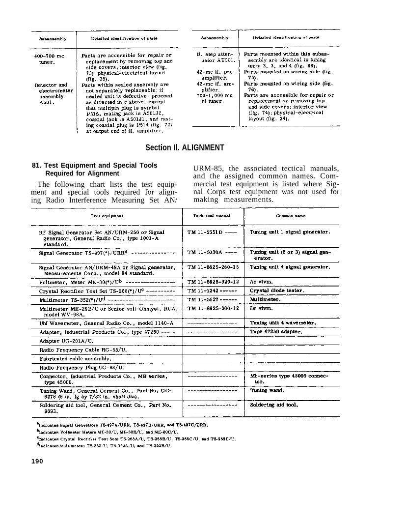
Section Il. ALIGNMENT
81. Test Equipment and Special ToolsRequired for Alignment
URM-85, the associated tectical manuals,and the assigned common names. Com-
The following chart lists the test equip- mercial test equipment is listed where Sig-ment and special tools required for align- nal Corps test equipment was not used foring Radio Interference Measuring Set AN/ making measurements.
190
82. Characteristics and Use of LaboratoryTest Equipment, and Special ToolsRequired for Alignment
The type of laboratory test equipmentand the special tools required for align-ment of the various tuning units are indi-cated in a through k b e l o w .
a. Tuning Unit 1 Signal Generator. Acw signal generator is required that canproduce output within the frequency rangefrom 150 kc to 30 mc at an accuracy of+1 percent. An output voltage from 0.05microvolt to 100 millivolts must be avail-able. The output impedance at the attenua-tor jack must be 50 ohms. This impedanceis obtained when the type 1OOO-P2 40-ohmseries unit (supplied with this signal gen-erator) is inserted into the attenuator out-put jack.
b. Tuning Unit 4 Signal Generator. A cwsignal generator is required that can pro-duce output within the frequency rangefrom 400 to 1,000 mc at an accuracy of±0.5 percent. An output voltage must beavailable which is continuously variablefrom 0.1 microvolt to approximately 1 volt,across a 50 ohm load.
c. Tuning Unit 4 Wavemeter. A wave-meter is required for checking the operat-ing frequency of the rf amplifier and oscil-lator in the 700-1,000-mc band of tuningunit 4. This wave meter covers the fre-quency range from 250 to 1,250 mc and isaccurate to within ±2 percent of its dialfrequency.
d. Dc Vtvm. This is a vacuum tube volt-meter (vtvm) capable of measuring ac anddc voltages from 0 to 1,500 volts and re-sistance from 0.2 ohm to 1,000 megohms.It has a dc input resistance of 11 megohms.
e. Type 472S0 Adapter. This is an adap-ter for converting a UG88/U connector toan md (minature bayonet) Industrial Pro-ducts Co. type 45000 connector, and is re-quired in aligning tuning unit 1 if. ampli-f i e r .
f . U G - 2 0 1 A / U A d a p t e r . T h i s i s a nadapter for connecting the UG-88/U con-nector to the N-series SIGNAL INPUT jackon the main unit front panel. It is requiredin al igning the tuning uni t 1 rf tuner .
g. Fabricated Cable Assembly. The fab-
ricated cable assembly consists of a 4-footlength of RG-55/U cable terminated by aUG-88/U connector, BNC-type, and an mb-series type 45000 connector . This cableis used in aligning the tuning unit 2 and 4if . amplif iers .
h. UG-88/U Plug. This male-type BNC-series connector terminates the RG-55/Ucoaxial cable.
i . Mb-Ser ies Type 45000 Connec tor .This female minature bayonet series con-nec to r t e rmina tes the RG-55 /U coax ia lcable.
j. Tuning Wand. This i s a 6 - inch by7/32-inch tuning wand used for adjustingthe co i l s ( tun ing un i t 2 ) and va r i ab lecapacitors (tuning unit 3).
k. Soldering Aid Tool. The soldering aidis used for beiding the split rotor bladesof the tuning capacitors during the align-ment of the rf sections of tuning units 3and 4.
83. Filament-Voltage and ±400 -VoItAdjustments
Remove the main unit from its instrumentcase (para 40b, item 12, TM 11-6625-351-12) and make the following adjustments inthe power supply section of the main unitbefore proceeding with the alignment.
a. ± 420-Volt Adjustment.(1)
(2)
(3)
(4)
Set POLARITY switch S709 at +.This switch is accessible from thetop of the main unit adjacent to thev o l t a g e r e g u l a t o r a s s e m b l y(fig. 52) .Connect the posi t ive lead of themultimeter to the top right termi-nal (1) of toggle switch S709 (fig.52). Connect the negative lead of themultimeter to chassis ground. Setthe multimeter FUNCTION switchto the DIRECT position.Set the main unit POWER switch atON.I M P U L S E G E N L E V E L S E Tcontrol R762 is a dual potentiom-eter which is mounted directly be-neath POLARITY switch S709 (fig.52) on the partition which separatesthe power supply from the bottomdeck of the main chassis. Vary the
191
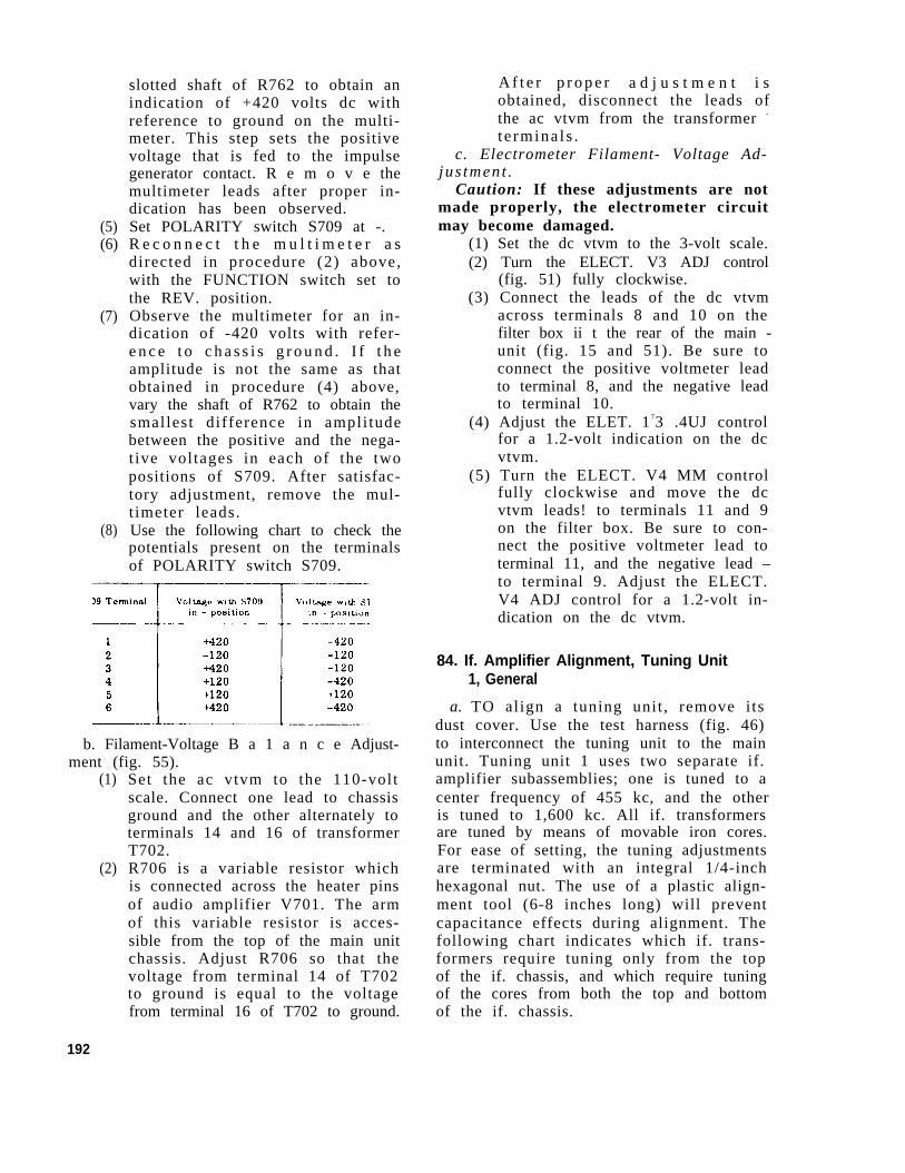
(5)(6)
(7)
(8)
slotted shaft of R762 to obtain anindication of +420 volts dc withreference to ground on the multi-meter. This step sets the positivevoltage that is fed to the impulsegenerator contact. R e m o v e themultimeter leads after proper in-dication has been observed.Set POLARITY switch S709 at -.R e c o n n e c t t h e m u l t i m e t e r a sdirected in procedure (2) above,with the FUNCTION switch set tothe REV. position.Observe the multimeter for an in-dication of -420 volts with refer-e n c e t o c h a s s i s g r o u n d . I f t h eamplitude is not the same as thatobtained in procedure (4) above,vary the shaft of R762 to obtain thesmallest difference in ampli tudebetween the positive and the nega-t ive voltages in each of the twopositions of S709. After satisfac-tory adjustment, remove the mul-t imeter leads.Use the following chart to check thepotentials present on the terminalsof POLARITY switch S709.
b. Filament-Voltage B a 1 a n c e Adjust-ment (fig. 55).
(1)
(2)
Set the ac vtvm to the 110-voltscale. Connect one lead to chassisground and the other alternately toterminals 14 and 16 of transformerT702.R706 is a variable resistor whichis connected across the heater pinsof audio amplifier V701. The armof this variable resistor is acces-sible from the top of the main unitchassis. Adjust R706 so that thevoltage from terminal 14 of T702to ground is equal to the voltagefrom terminal 16 of T702 to ground.
A f t e r p r o p e r a d j u s t m e n t i sobtained, disconnect the leads ofthe ac vtvm from the transformer -
t e rmina l s .c. Electrometer Filament- Voltage Ad-
jus tmen t .Caution: If these adjustments are not
made properly, the electrometer circuitmay become damaged.
(1) Set the dc vtvm to the 3-volt scale.(2) Turn the ELECT. V3 ADJ control
(fig. 51) fully clockwise.(3) Connect the leads of the dc vtvm
across terminals 8 and 10 on thefilter box ii t the rear of the main -unit (fig. 15 and 51). Be sure toconnect the positive voltmeter leadto terminal 8, and the negative leadto terminal 10.
(4) Adjust the ELET. 1 73 .4UJ controlfor a 1.2-volt indication on the dcvtvm.
(5) Turn the ELECT. V4 MM controlfully clockwise and move the dcvtvm leads! to terminals 11 and 9on the filter box. Be sure to con-nect the positive voltmeter lead toterminal 11, and the negative lead –to terminal 9. Adjust the ELECT.V4 ADJ control for a 1.2-volt in-dication on the dc vtvm.
84. If. Amplifier Alignment, Tuning Unit1, General
a. TO align a tuning unit , remove i tsdust cover. Use the test harness (fig. 46)to interconnect the tuning unit to the mainunit. Tuning unit 1 uses two separate if.amplifier subassemblies; one is tuned to acenter frequency of 455 kc, and the otheris tuned to 1,600 kc. All if. transformersare tuned by means of movable iron cores.For ease of setting, the tuning adjustmentsare terminated with an integral 1/4-inchhexagonal nut. The use of a plastic align-ment tool (6-8 inches long) will preventcapacitance effects during alignment. Thefollowing chart indicates which if. trans-formers require tuning only from the topof the if. chassis, and which require tuningof the cores from both the top and bottomof the if. chassis.
192
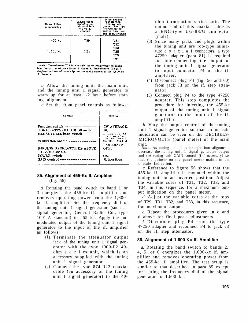
b. Allow the tuning unit, the main unit,and the tuning unit 1 signal generator towarm up for at least 1/2 hour before start-ing alignment.
c. Set the front panel controls as follows:
85. Alignment of 455-Kc If. Amplifier(fig. 56)
a. Rotating the band switch to band 1 or3 energizes the 455-kc if. amplifier andremoves operating power from the 1,600-kc if. amplifier. Set the frequency dial ofthe tuning unit 1 signal generator (such assignal generator, General Radio Co., type1001-A standard) to 455 kc. Apply the un-modulated output of the tuning unit 1 signalgenerator to the input of the if. amplifieras follows:
(1)
(2)
Termina te the a t t enua to r ou tpu tjack of the tuning unit 1 signal gen-erator with the type 1000-P2 40-ohm s e r i es unit, which is anaccessory supplied with the tuningunit 1 signal generator.Connect the type 874-R22 coaxialcable (an accessory of the tuningunit 1 signal generator) to the 40-
(3)
(4)
(5)
ohm termination series unit . Theoutput end of this coaxial cable isa BNC- type UG-88/U connec tor(male).Since many jacks and plugs withinthe tuning unit are rob-type minia-ture c o a x i a 1 connectors, a type47250 adapter (para 81) is requiredfor interconnecting the output ofthe tuning unit 1 signal generatorto input comector P4 of the if .amplif ier .Disconnect plug P4 (fig. 56 and 60)from jack J3 on the if. step atten-ua to r .Connect plug P4 to the type 47250adapter . This s tep completes theprocedure for injecting the 455-kcoutput of the tuning unit 1 signalgenerator to the input of the i f .amplif ier .
b. Vary the output control of the tuningunit 1 signal generator so that an onscaleindication can be seen on the DECIBELS-MICROVOLTS (panel meter) of the mainunit.
Note: As tuning unit 1 is brought into alignment,decrease the tuning unit 1 signal generator outputand the tuning unit GAIN control (i f necessary) sothat the pointer on the panel meter maintains anonscale indication.
c. Reference to figure 56 shows that the455-kc if. amplifier is mounted within thetuning unit in an inverted position. Adjustthe variable cores of T31, T32, T33, andT34, in this sequence, for a maximum out-put indication on the panel meter.
d. Adjust the variable cores at the topsof T29, T31, T32, and T33, in this sequence,for maximum output.
e. Repeat the procedures given in c andd above for final peak adjustments.
f. Disconnec t p lug P4 f rom the type47250 adapter and reconnect P4 to jack J3on the if. step attenuator.
86. Alignment of 1,600-Kc If. Amplifier
a. Rotating the band switch to bands 2,4, 5, or 6 energizes the 1,600-kc if. am-plifier and removes operating power fromthe 455-kc if. amplifier. The test setup issimilar to that described in para 85 exceptfor setting the frequency dial of the signalgenerator to 1,600 kc.
193
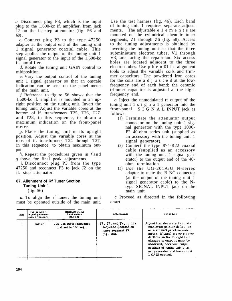
Figure 58.
b. Disconnect plug P3, which is the inputplug to the 1,600-kc if. amplifier, from jackJ2 on the if. step attenuator (fig. 56 and60) .
c. Connect plug P3 to the type 47250adapter at the output end of the tuning unit1 signal generator coaxial cable. Thisstep applies the output of the tuning unit 1signal generator to the input of the 1,600-kcif. amplifier.
d. Rotate the tuning unit GAIN control tomidposition.
e. Vary the output control of the tuningunit 1 signal generator so that an onscaleindication can be seen on the panel meterof the main unit.
f. Reference to figure 56 shows that the1,600-kc if. amplifier is mounted in an up-right position on the tuning unit. Invert thetuning unit. Adjust the variable cores at thebottom of if. transformers T25, T26, T27.and T28, in this sequence, to obtain amaximum indication on the front-panelmeter.
g. Place the tuning unit in its uprightposition. Adjust the variable cores at thetops of if. transformers T24 through T27,in this sequence, to obtain maximum out-put .
h. Repeat the procedures given in f andg above for final peak adjustments.
i. Disconnect plug P3 from the type47250 and reconnect P3 to jack J2 on theif. step attenuator.
87. Alignment of Rf Tuner Section,Tuning Unit 1
(fig. 56)
a. To align the rf tuner, the tuning unitmust be operated outside of the main unit.
Use the test harness (fig. 46). Each bandof tuning unit 1 requires separate adjust-ments. The adjustable e 1 e m e n t s aremounted on the cylindrical phenolic tunersegments, Z1 through Z6 (fig. 58). Accessto the tuning adjustments is obtained byinverting the tuning unit so that the threesubminiature electron tubes, V1 throughV3, are facing the repairman. Six accessholes are located adjacent to the threeelectron tubes. Use p h e n 01 i c alignmenttools to adjust the variable coils and trim-mer capacitors. The powdered iron coresfor the coils are a d j u s t e d at the low-frequency end of each band; the ceramictrimmer capacitor is adjusted at the high-frequency end.
b. Inject the unmodulated rf output of thetuning unit 1 s i g n a 1 generator into thefront-panel S I G N A L INPUT jack asfollows:
(1)
(2)
(3)
Terminate the attenuator outputconnector on the tuning unit 1 sig-nal generator with the type 1000-P2 40-ohm series unit (supplied asan accessory with the tuning unit 1signal generator).Connect the type 874-R22 coaxialcable (supplied as an accessorywith the tuning unit 1 signal gen-erator) to the output end of the 40-ohm termination.Use the UG-201A/U N-ser iesadapter to mate the B NC connector(at the output of the tuning unit 1signal generator cable) to the N-type SIGNAL INPUT jack on themain unit.
c. Proceed as directed in the followingchart.
194
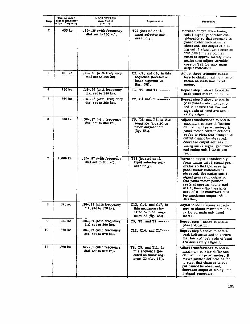
195
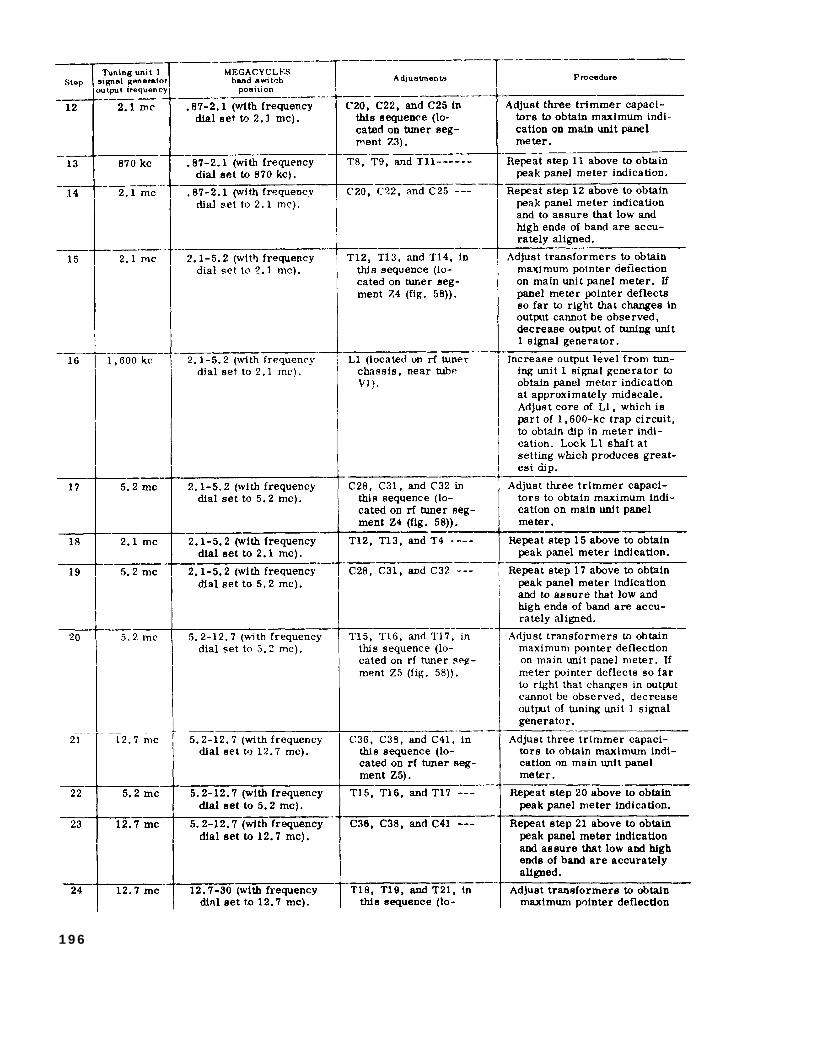
1 9 6
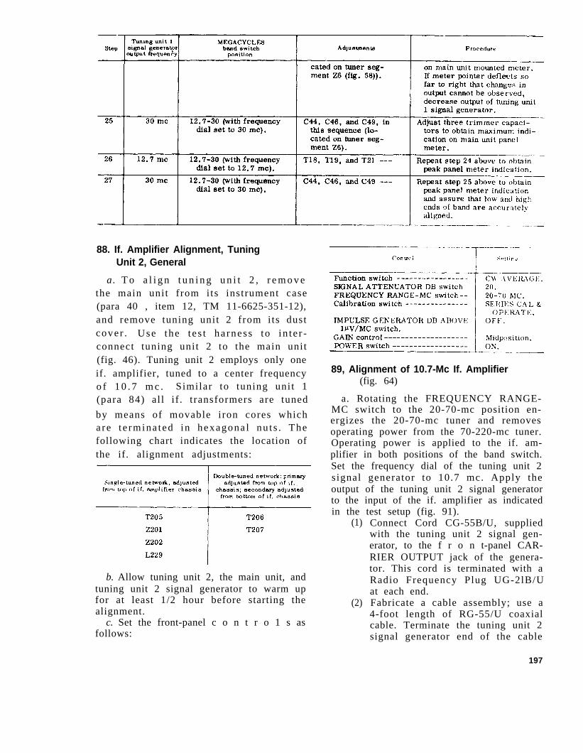
88. If. Amplifier Alignment, TuningUnit 2, General
a. T o a l i g n t u n i n g u n i t 2 , r e m o v ethe main unit from i ts instrument case(para 40 , item 12, TM 11-6625-351-12),and remove tuning unit 2 from i ts dustcover . Use the t e s t ha rness to in t e r -connect tuning unit 2 to the main unit(fig. 46). Tuning unit 2 employs only oneif. amplifier, tuned to a center frequencyo f 1 0 . 7 m c . Similar to tuning uni t 1(para 84) al l i f . t ransformers are tuned
by means of movable iron cores whichare t e rmina ted in hexagona l nu t s . Thefollowing chart indicates the location ofthe if. alignment adjustments:
b. Allow tuning unit 2, the main unit, andtuning unit 2 signal generator to warm upfor at least 1/2 hour before starting thealignment.
c. Set the front-panel c o n t r o 1 s asfollows:
89, Alignment of 10.7-Mc If. Amplifier(fig. 64)
a. Rotating the FREQUENCY RANGE-MC switch to the 20-70-mc position en-ergizes the 20-70-mc tuner and removesoperating power from the 70-220-mc tuner.Operating power is applied to the if. am-plifier in both positions of the band switch.Set the frequency dial of the tuning unit 2signal generator to 10.7 mc. Apply theoutput of the tuning unit 2 signal generatorto the input of the if. amplifier as indicatedin the test setup (fig. 91).
(1)
(2)
Connect Cord CG-55B/U, suppliedwith the tuning unit 2 signal gen-erator, to the f r o n t-panel CAR-RIER OUTPUT jack of the genera-tor. This cord is terminated with aRadio Frequency Plug UG-2lB/Uat each end.Fabricate a cable assembly; use a4-foot length of RG-55/U coaxialcable. Terminate the tuning unit 2signal generator end of the cable
197
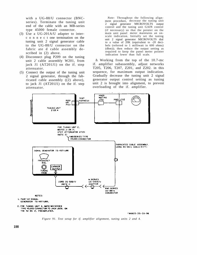
(3)
(4)
(5)
with a UG-88/U connector (BNC-series). Terminate the tuning unitend of the cable with an MB-seriestype 45000 female connector.Use a UG-201A/U adapter to inter-c o n n e c t one termination on thetuning unit 2 signal generator cableto the UG-88/U connector on thefabric ate d cable assembly de-scribed in (2) above.Disconnect plug P209 on the tuningunit 2 cable assembly W201, fromjack J1 (AT201J1) on the if. stepat tenuator .Connect the output of the tuning unit2 signal generator, through the fab-ricated cable assembly ((2) above),to jack J1 (AT201J1) on the if. stepat tenuator .
Note: Throughout the following align-ment procedure, decrease the tuning unit2 signal generator MICROVOLTS outputcontrol and the tuning unit GAIN control(if necessary) so that the pointer on themain unit panel meter maintains an on-scale indication. Initially set the tuningunit 2 signal generator MICROVOLTS dialto a value of 20K (equivalent to -20 deci-bels (referred to 1 milliwatt in 600 ohms)(dbm)); then reduce the output setting asrequired to keep the panel meter pointerindication lower than full scale.
b. Working from the top of the 10.7-mcif. amplifier subassembly, adjust networksT205, T206, T207, Z201, and Z202. in thissequence, for maximum output indication.Gradually decrease the tuning unit 2 signalgenerator output control setting as tuningunit 2 is brought into alignment, to preventoverloading of the if. amplifier.
Figure 91. Test setup for if. amplifier alignment, tuning units 2 and 4.
198
C . Working from the bottom of the 10.7-mc if. amplifier subassembly, adjust thecores of if. transformers T206 and T207for a further maximum indication on thepanel meter.
d. Repeat the procedures given in b a n dc a b o v e , as necessary, unti l no furtherpeaking can be observed. Proper if. align-ment is evidenced when an output of ap-proximately 40 to 70 microvolt from thetuning unit 2 signal generator produces afull-scale pointer deflection on the panelmeter (with the SIGNAL ATTENUATORDB switch at the 20 db position).
e. After completing the p r o c e d u r esgiven in a through d above, adjust signalpeaking coil L229 in the cathode circuitof V211, as follows:
(1)
(2)
(3)
(4)
(5)
(6)
(7)
IF. CATHODE FOLLOWER ADJswi tch S704 i s moun ted on themain unit power supply partition(fig. 51). Set this toggle switch tothe open-circuit position to place aresistor in the metering signal pathand make the panel meter (M701)less sensitive.Observe that the meter pointer nowdeflects to approximate midscale,with the tuning unit 2 signal gener-ator i n j e c t i n g a 50-microvoltoutput signal (at 10.7 mc) into theif. amplifier.Rotate the tuning unit 2 signal gen-erator MICROVOLTS control toobtain the full-power level capa-b i l i t y ( a p p r o x i m a t e l y 1 0 0 , 0 0 0microvolt), and adjust the core ofL229 for a maximum output indica-tion on the panel meter.Set switch S704 to its closed-cir-cui t posi t ion. This act ion short-circuits the series resistor in themetering signal path and causes thepanel meter to be more sensitive.Decrease the tuning unit 2 signalgenerator MICROVOLTS control tothe setting that produces approxi-m a t e m i d s c a l e p a n e l m e t e rreading.Readjust Z202 to obtain a maximumpanel meter indication.Repeat the procedures given in (1)through (6) above for f inal peak
panel meter indication. This pro-cedure completes the alignment ofthe 10.7-mc if. amplifier.
f. Disconnect the fabricated cable as-sembly (a(2) above) from input jack J1 onthe if. step attenuator. Reconnect plug P209on cable assembly W201 to input jack J1 onthe if. step attenuator.
90. Using Tuning Wand
A tuning wand is required for aligningthe 70-200-mc band of tuning - unit 2 andfor the complete frequency range of tuningunit 3. This tuning wand, which is commer-cial ly available, consists of a plexiglasrod approximately 7/32 inch in diameterby 6 inches long. One end of the wand ter-minates in a powdered iron core slug; theother end terminates in a brass slug. Usethe wand as described below:
a. Tuning Unit 2 (70- to 220-Mc Band(fig. 65)).
(1)
(2)
Insert the brass s lug end of thetuning wand into the separate mag-netic field of variable coils L208 atthe input to V204, L211 at the inputto V205, and L213 at the input toV206A. Watch the change in indica-tion on the main unit panel meter.An increase in the meter indicationshows that the coupling between theindividual loops of wire comprisingthe particular coil under measure-ment should be reduced. This effectis obtained by spreading the loopsof wi re fa r the r apar t f rom eachother .Insert the powdered iron core endof the tuning wand into the samevariable coils, one coil at a time.Watch the change in panel meter in-dication. An increase in the panelmeter indication with the powderediron core inserted in the magneticfield of the coil now shows that thecoupling between the loops of wire
69)).
shoul be increased. This effect iso b t a i n e d b y b e n d i n g t h e l o o p scloser to each other.
b. Tuning Unit 3 (200 to 400 Mc ( f ig .
1) Insert the brass s lug end of the
199
(2)
tuning wand into the magnetic fieldof the coupling loops such as thefield created by rf energy in thevicini ty of L401-L402, or L404-L405. Observe the change in meterindication. An i n c r e as e in themeter indicat ion shows the need
for reducing the coupling between
the pickup loops. This effect is ob-
tained by farther spacing b e t w e e nthe primary and . the secondary
loops lInsert the powdered iron core end
91. Alignment of Rf Tuner Section,Tuning Unit 2
(fig. 64 and 65)
Warning: Various inductances in the rftuner section of tuning unit 2 (fig. 65) re-quire squeezing or spreading turns of un-insulated wire. Never touch these induct-ances with the bare fingers while operatingpower is applied, since B+ potentials of105 volts and 150 volts are present. Alwaysuse a well- insulated pair of pliers orsimilar tool for squeezing or spreadingthe turns of wire. Also be careful to avoidshort-circuiting one t u r n of wire toanother.
of the wand into the magnetic fieldsurrounding the pickup loops undermeasurement, and o b s e r v e thechange in meter indication. An in-
c rease in me te r ind ica t ion nowshows the need for increasing t h ecoupling between the pickup loops.
This effect is obtained by closer
spacing between the primary and
secondary loops.
a. Align the rf tuner while tuning unit2 is operating outside the main unit. Usethe test harness (fig. 46), with the frontpanel control set to the positions listed inparagraph 88.
b. Remove the cover from the exteriorside of the rf tuner (fig. 64).
c. Connect the output of the tuning unit 2signal generator, through Cord CG-55B/Usupplied with the signal generator, to themain unit front panel SIGNAL INPUT jack.Proceed as directed in the following chart:
2 0 0

201
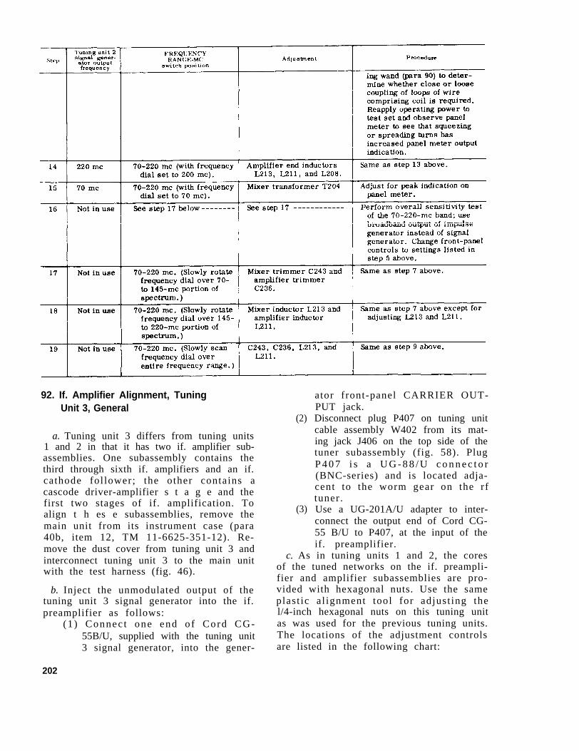
92. If. Amplifier Alignment, TuningUnit 3, General
a. Tuning unit 3 differs from tuning units1 and 2 in that it has two if. amplifier sub-assemblies. One subassembly contains thethird through sixth if. amplifiers and an if.cathode fol lower; the other contains acascode driver-amplifier s t a g e and thefirst two stages of if. amplification. Toalign t h es e subassemblies, remove themain unit from its instrument case (para40b, item 12, TM 11-6625-351-12). Re-move the dust cover from tuning unit 3 andinterconnect tuning unit 3 to the main unitwith the test harness (fig. 46).
b. Inject the unmodulated output of thetuning unit 3 signal generator into the if.preamplifier as follows:
(1 ) Connec t one end o f Cord CG-55B/U, supplied with the tuning unit3 signal generator, into the gener-
202
(2)
(3)
ator front-panel CARRIER OUT-PUT jack.Disconnect plug P407 on tuning unitcable assembly W402 from its mat-ing jack J406 on the top side of thetuner subassembly (fig. 58). PlugP 4 0 7 i s a U G - 8 8 / U c o n n e c t o r(BNC-series) and is located adja-cent to the worm gear on the rftuner.Use a UG-201A/U adapter to inter-connect the output end of Cord CG-55 B/U to P407, at the input of theif. preamplifier.
c. As in tuning units 1 and 2, the coresof the tuned networks on the if. preampli-fier and amplifier subassemblies are pro-vided with hexagonal nuts. Use the sameplast ic al ignment tool for adjust ing thel/4-inch hexagonal nuts on this tuning unitas was used for the previous tuning units.The locations of the adjustment controlsare listed in the following chart:
d. Set the front-panel controls on thetest set as listed in paragraph 88c exceptfor the FREQUENCY RANGE MC switch.Tuning unit 3 has no band switch.
93. Alignment of 42-Mc If. Amplifiers
a. Set the frequency dial of the tuningunit 3 signal generator to 42 mc and injectthe output signal into if. preamplifier cableassembly W402.
b. Set the MICROVOLTS control of thetuning unit 3 signal generator to producean approximate midscale reading on themain unit panel meter.
c. The 42-mc if. amplifier subassemblyis mounted in a horizontal position at thetop of tuning unit 3. Working from the elec-tron tube side of the 42-mc if. amplifiersubassembly, adjust the cores of networksZ403, T408, T407, T406, and T405, in thissequence, to obtain a maximum panel meterindication. As the 42-mc if. amplifier isbrought into alignment, decrease the MI-CROVOLTS control setting on the tuningunit 3 s i g n a l generator and the GAINcontrol setting (if necessary) on the frontpanel to maintain an onscale panel meterindication.
d. Working from the tube socket side of42-mc if . amplif ier subassembly, adjustthe cores of networks T408, T407, andT406 to obtain a further peak indication onthe panel meter.
Note: If the 42-mc if. amplifier cannot be alignedwith the tuning unit 3 signal generator connected topreamplifier cable assembly W402, connect the tun-ing unit 3 signal generator to cable assembly W403(connector P409) and repeat the procedures givenin b, c, and d above.
e. The 42-mc i f . p reampl i f i e r subas -sembly is also mounted at the top of tuningunit 3, with the electron tubes in an in-verted position. W o r k from the electrontube side of this subassembly and adjustthe cores of networks Z402, Z401, and T401to obtain a maximum panel meter indica-tion.
f. After completing the procedures givenin a through e above, align signal peakingcoil L431, in if. cathode follower stageV410, as follows:
(1)
(2)
(3)
(4)
(5)
Set IF . CATHODE FOLLOWERADJ switch S704 on the main unitpower supply partition (fig. 51) tothe open-circuited position.O b s e r v e t h a t t h e p a n e l m e t e rpo in te r de f l ec t s to approx imatemidscale, with the tuning unit 3 sig-nal g e n e r a t o r injecting a 12-microvolt output signal (at 42 mc)into the 42-mc if. amplifier.Ro ta t e t he tun ing un i t 3 s igna lgenerator MICROVOLTS control toobtain the full-power leve1 capa-bi l i ty from the signal generator .Adjust the core of L431 (fig. 71) fora maximum output indication on thepanel meter.Set switch S704 to its c 1 o s e d-circui t posi t ion and see that thepane l me te r po in te r ind ica tes afull-scale reading.Repeat the procedures given in (1)through (4) above to assure that a1 2 - m i c r o v o l t o u t p u t f r o m t h etuning unit 3 signal generator pro-duces a f u 1 l-scale panel meterindication, while the SIGNAL AT-TENUATOR DB switch on the mainunit front panel set to the 20-dbposition.
g. After meeting the requirement in fabove, disconnect the output of the tuningunit 3 signal generator from plug P407 oncable assembly W402. Reconnect P407 toits mating jack, J406, at the top of the rftuner (fig. 58). This procedure enables theoutput of the rf tuner to pass through thei f . ampl i f i e r , t h rough the de tec to r andelectrometer assembly, and to the meter-ing circuit in the main unit e
203
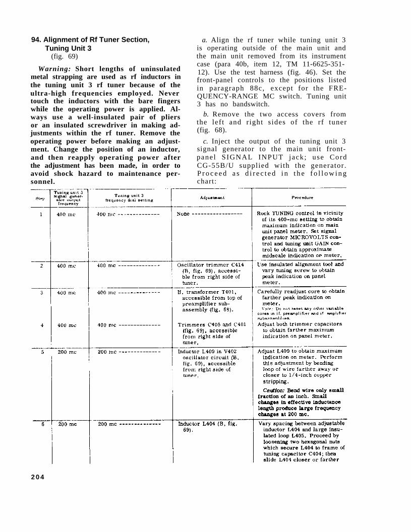
94. Alignment of Rf Tuner Section,Tuning Unit 3
(fig. 69)
Warning: Short lengths of uninsulatedmetal strapping are used as rf inductors inthe tuning unit 3 rf tuner because of theultra-high frequencies employed. Nevertouch the inductors with the bare fingerswhile the operating power is applied. Al-ways use a well-insulated pair of pliersor an insulated screwdriver in making ad-justments within the rf tuner. Remove theoperating power before making an adjust-ment. Change the position of an inductor,and then reapply operating power afterthe adjustment has been made, in order toavoid shock hazard to maintenance per-sonnel.
a. Align the rf tuner while tuning unit 3is operating outside of the main unit andthe main unit removed from its instrumentcase (para 40b, item 12, TM 11-6625-351-12). Use the test harness (fig. 46). Set thefront-panel controls to the positions listedin paragraph 88c, except for the FRE-QUENCY-RANGE MC switch. Tuning unit3 has no bandswitch.
b. Remove the two access covers fromthe lef t and r ight s ides of the rf tuner(fig. 68).
c. Inject the output of the tuning unit 3signal generator to the main unit front-pane l SIGNAL INPUT jack ; use CordCG-55B/U supplied with the generator .P r o c e e d a s d i r e c t e d i n t h e f o l l o w i n gchart:
2 0 4
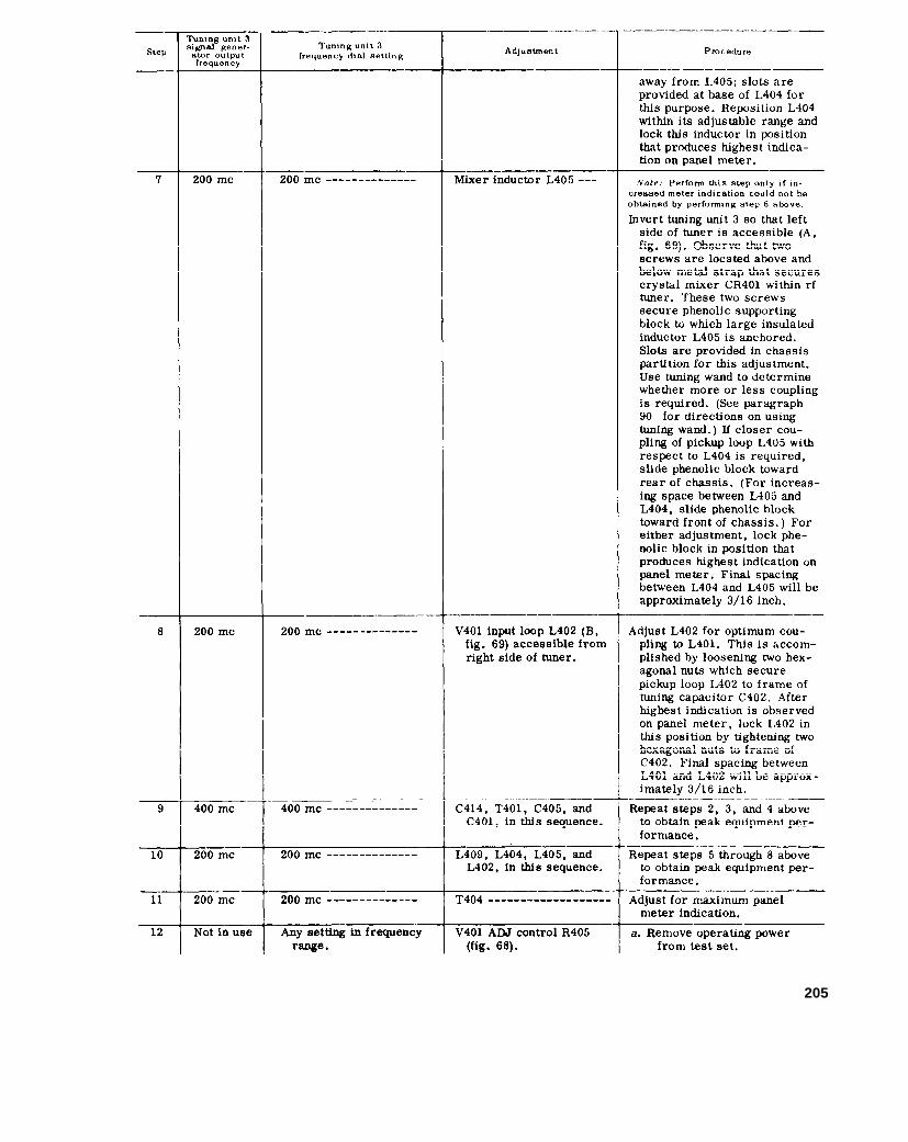
205
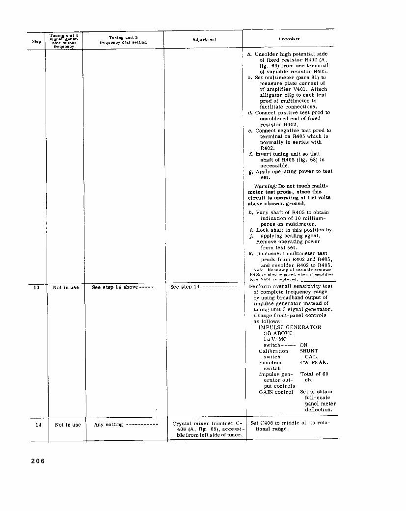
2 0 6
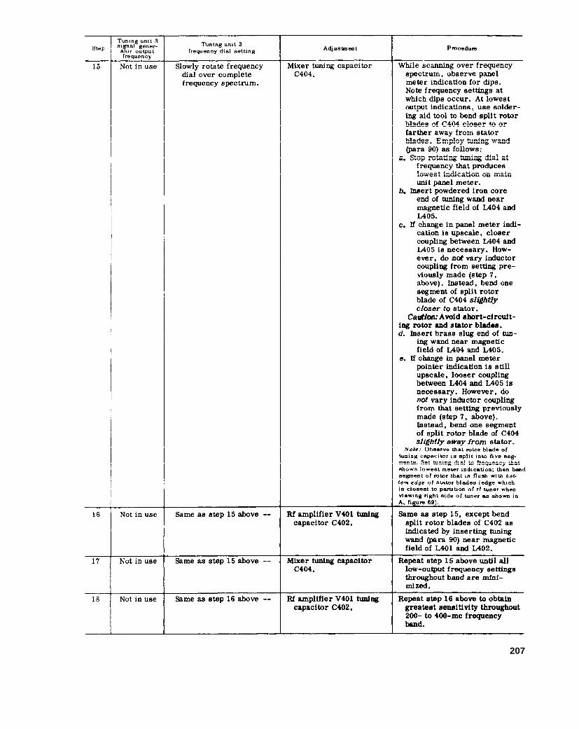
207
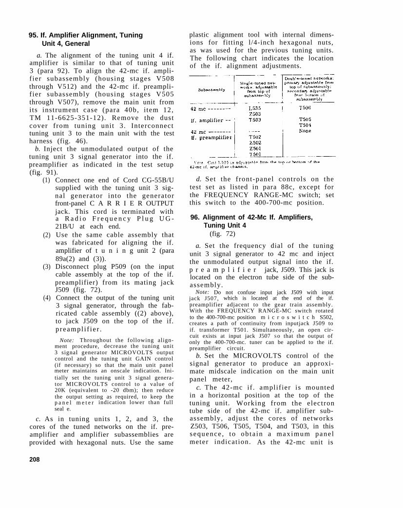
95. If. Amplifier Alignment, TuningUnit 4, General
a. The alignment of the tuning unit 4 if.amplifier is similar to that of tuning unit3 (para 92). To align the 42-mc if. ampli-f ier subassembly (housing stages V508through V512) and the 42-mc if. preampli-f ier subassembly (housing stages V505through V507), remove the main unit fromits instrument case (para 40b, i tem 12,TM 11-6625-351-12). Remove the dustcover from tuning unit 3. Interconnecttuning unit 3 to the main unit with the testharness (fig. 46).
b. Inject the unmodulated output of thetuning unit 3 signal generator into the if.preamplifier as indicated in the test setup(fig. 91).—
(1)
(2)
(3)
(4)
Connect one end of Cord CG-55B/Usupplied with the tuning unit 3 sig-nal generator into the generatorfront-panel C A R R I E R OUTPUTjack. This cord is terminated witha R a d i o F r e q u e n c y P l u g U G -21B/U at each end.Use the same cable assembly thatwas fabricated for aligning the if.amplifier of t u n i n g unit 2 (para89a(2) and (3)).Disconnect plug P509 (on the inputcable assembly at the top of the if.preamplifier) from its mating jackJ509 (fig. 72).Connect the output of the tuning unit3 signal generator, through the fab-ricated cable assembly ((2) above),to jack J509 on the top of the if.p reampl i f i e r .
Note: Throughout the following align-ment procedure, decrease the tuning unit3 signal generator MICROVOLTS outputcontrol and the tuning unit GAIN control(if necessary) so that the main unit panelmeter maintains an onscale indication. Ini-tially set the tuning unit 3 signal genera-tor MICROVOLTS control to a value of20K (equivalent to -20 dbm); then reducethe output setting as required, to keep thep a n e l m e t e r indication lower than fullseal e.
c. As in tuning units 1, 2, and 3, thecores of the tuned networks on the if. pre-amplifier and amplifier subassemblies areprovided with hexagonal nuts. Use the same
plastic alignment tool with internal dimens-ions for fitting l/4-inch hexagonal nuts,as was used for the previous tuning units.The following chart indicates the locationof the if. alignment adjustments.
d. Set the front-panel controls on thetest set as listed in para 88c, except forthe FREQUENCY RANGE-MC switch; setthis switch to the 400-700-mc position.
96. Alignment of 42-Mc If. Amplifiers,Tuning Unit 4
(fig. 72)
a. Set the frequency dial of the tuningunit 3 signal generator to 42 mc and injectthe unmodulated output signal into the if.p r e a m p l i f i e r jack, J509. This jack islocated on the electron tube side of the sub-assembly.
Note: Do not confuse input jack J509 with inputjack J507, which is located at the end of the if.preamplifier adjacent to the gear train assembly.With the FREQUENCY RANGE-MC switch rotatedto the 400-700-mc position m i c r o s w i t c h S502,creates a path of continuity from inputjack J509 toif. transformer T501. Simultaneously, an open cir-cuit exists at input jack J507 So that the output ofonly the 400-700-mc. tuner can be applied to the if.preamplifier circuit.
b. Set the MICROVOLTS control of thesignal generator to produce an approxi-mate midscale indication on the main unitpanel meter,
c. The 42-mc if . amplif ier is mountedin a horizontal position at the top of thetuning unit. Working from the electrontube side of the 42-mc if. amplifier sub-assembly, adjust the cores of networksZ503, T506, T505, T504, and T503, in thissequence , to ob ta in a max imum pane lmeter indicat ion. As the 42-mc unit is
208
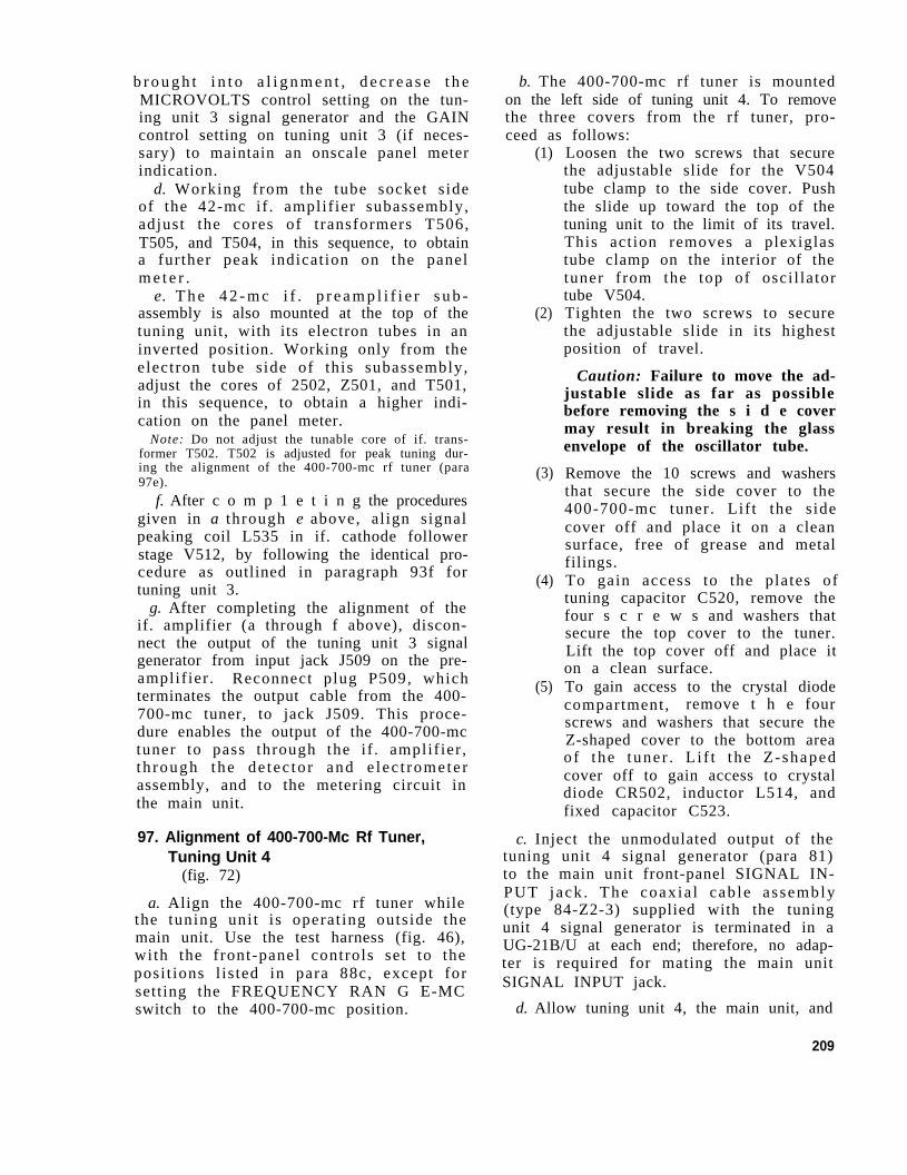
b r o u g h t i n t o a l i g n m e n t , d e c r e a s e t h eMICROVOLTS control setting on the tun-ing unit 3 signal generator and the GAINcontrol setting on tuning unit 3 (if neces-sary) to maintain an onscale panel meterindication.
d. Working from the tube socket s ideof the 42-mc if . amplif ier subassembly,adjust the cores of t ransformers T506,T505, and T504, in this sequence, to obtaina further peak indication on the panelm e t e r .
e. T h e 4 2 - m c i f . p r e a m p l i f i e r s u b -assembly is also mounted at the top of thetuning unit, with its electron tubes in aninverted position. Working only from theelectron tube side of this subassembly,adjust the cores of 2502, Z501, and T501,in this sequence, to obtain a higher indi-cation on the panel meter.
Note: Do not adjust the tunable core of if. trans-former T502. T502 is adjusted for peak tuning dur-ing the alignment of the 400-700-mc rf tuner (para97e).
f. After c o m p 1 e t i n g the proceduresgiven in a through e above, al ign signalpeaking coil L535 in if. cathode followerstage V512, by following the identical pro-cedure as outlined in paragraph 93f fortuning unit 3.
g. After completing the alignment of theif. amplifier (a through f above), discon-nect the output of the tuning unit 3 signalgenerator from input jack J509 on the pre-amplif ier . Reconnect plug P509, whichterminates the output cable from the 400-700-mc tuner, to jack J509. This proce-dure enables the output of the 400-700-mctuner to pass through the if . amplif ier ,th rough the de tec to r and e lec t romete rassembly, and to the metering circuit inthe main unit.
97. Alignment of 400-700-Mc Rf Tuner,Tuning Unit 4
(fig. 72)
a. Align the 400-700-mc rf tuner whilethe tuning uni t is operat ing outside themain unit. Use the test harness (fig. 46),with the front-panel controls set to theposi t ions l is ted in para 88c, except forsetting the FREQUENCY RAN G E-MCswitch to the 400-700-mc position.
b. The 400-700-mc rf tuner is mountedon the left side of tuning unit 4. To removethe three covers from the rf tuner, pro-ceed as follows:
(1)
(2)
(3)
(4)
(5)
Loosen the two screws that securethe adjustable slide for the V504tube clamp to the side cover. Pushthe slide up toward the top of thetuning unit to the limit of its travel.This action removes a plexiglastube clamp on the interior of thetuner from the top of osci l latortube V504.Tighten the two screws to securethe adjustable slide in its highestposition of travel.
Caution: Failure to move the ad-justable slide as far as possiblebefore removing the s i d e covermay result in breaking the glassenvelope of the oscillator tube.
Remove the 10 screws and washersthat secure the side cover to the400-700-mc tuner. Lif t the sidecover off and place it on a cleansurface, free of grease and metalfilings.To gain access to the plates oftuning capacitor C520, remove thefour s c r e w s and washers thatsecure the top cover to the tuner.Lift the top cover off and place iton a clean surface.To gain access to the crystal diodecompartment, remove t h e fourscrews and washers that secure theZ-shaped cover to the bottom areaof the tuner . L i f t the Z-shapedcover off to gain access to crystaldiode CR502, inductor L514, andfixed capacitor C523.
c. Inject the unmodulated output of thetuning unit 4 signal generator (para 81)to the main unit front-panel SIGNAL IN-PUT jack . The coax ia l cab le assembly(type 84-Z2-3) supplied with the tuningunit 4 signal generator is terminated in aUG-21B/U at each end; therefore, no adap-ter is required for mating the main unitSIGNAL INPUT jack.
d. Allow tuning unit 4, the main unit, and
209
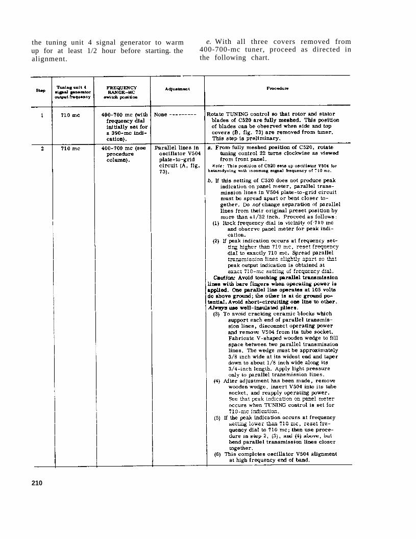
the tuning unit 4 signal generator to warm e. With all three covers removed fromup for at least 1/2 hour before starting the 400-700-mc tuner, proceed as directed inalignment.
—the following chart.
210
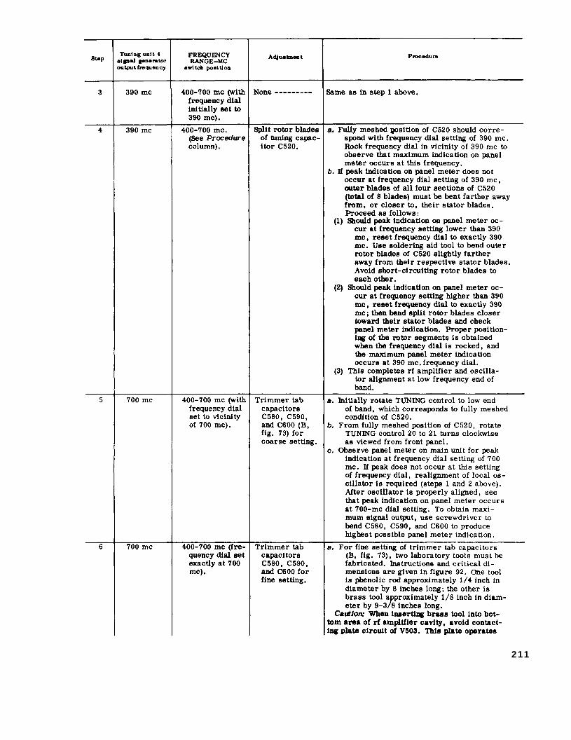
211
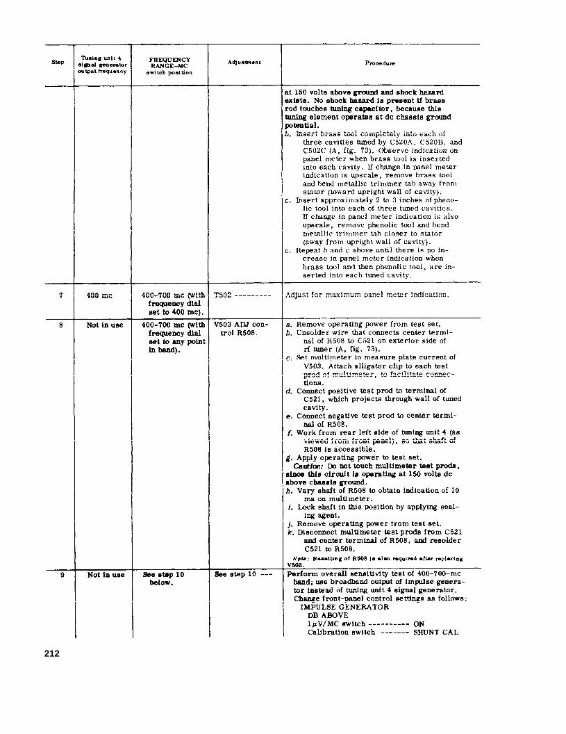
212
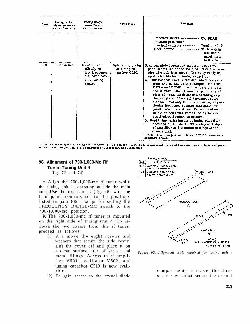
98. Alignment of 700-1,000-Mc RfTuner, Tuning Unit 4
(fig. 72 and 74)
a. Align the 700-1,000-mc rf tuner whilethe tuning unit is operating outside the mainunit. Use the test harness (fig. 46) with thefront-panel controls set to the positionslisted in para 88c, except for setting theFREQUENCY RANGE-MC switch to the700-1,000-mc position,
b. The 700-1,000-mc rf tuner is mountedon the right side of tuning unit 4. To re-move the two covers from this rf tuner,proceed as follows:
(1)
(2)
R e move the e igh t sc rews andwashers that secure the side cover.Lift the cover off and place it ona clean surface, free of grease andmetal filings. Access to rf ampli-f i e r V501 , osc i l l a to r V502 , andtuning capacitor C510 is now avail-able.To gain access to the crystal diode
Figure 92. Alignment tools required for tuning unit 4
compartment, r e m o v e t h e f o u rs c r e w s that secure the second
213
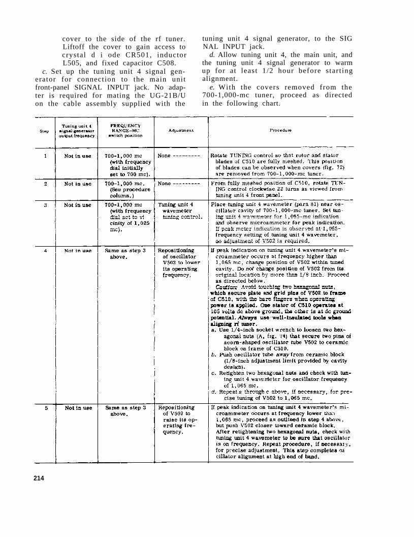
cover to the side of the rf tuner.Liftoff the cover to gain access tocrystal d i ode CR501, inductorL505, and fixed capacitor C508.
c. Set up the tuning unit 4 signal gen-erator for connection to the main unitfront-panel SIGNAL INPUT jack. No adap-ter is required for mating the UG-21B/Uon the cable assembly supplied with the
tuning unit 4 signal generator, to the SIGNAL INPUT jack.
d. Allow tuning unit 4, the main unit, andthe tuning unit 4 signal generator to warmup for at least 1/2 hour before s tar t ingalignment.
e. With the covers removed from the700-1,000-mc tuner, proceed as directedin the following chart.
214
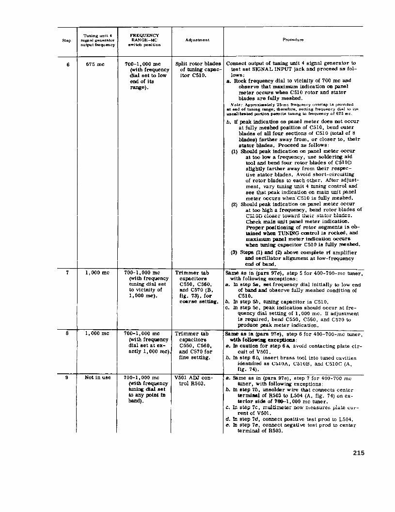
215
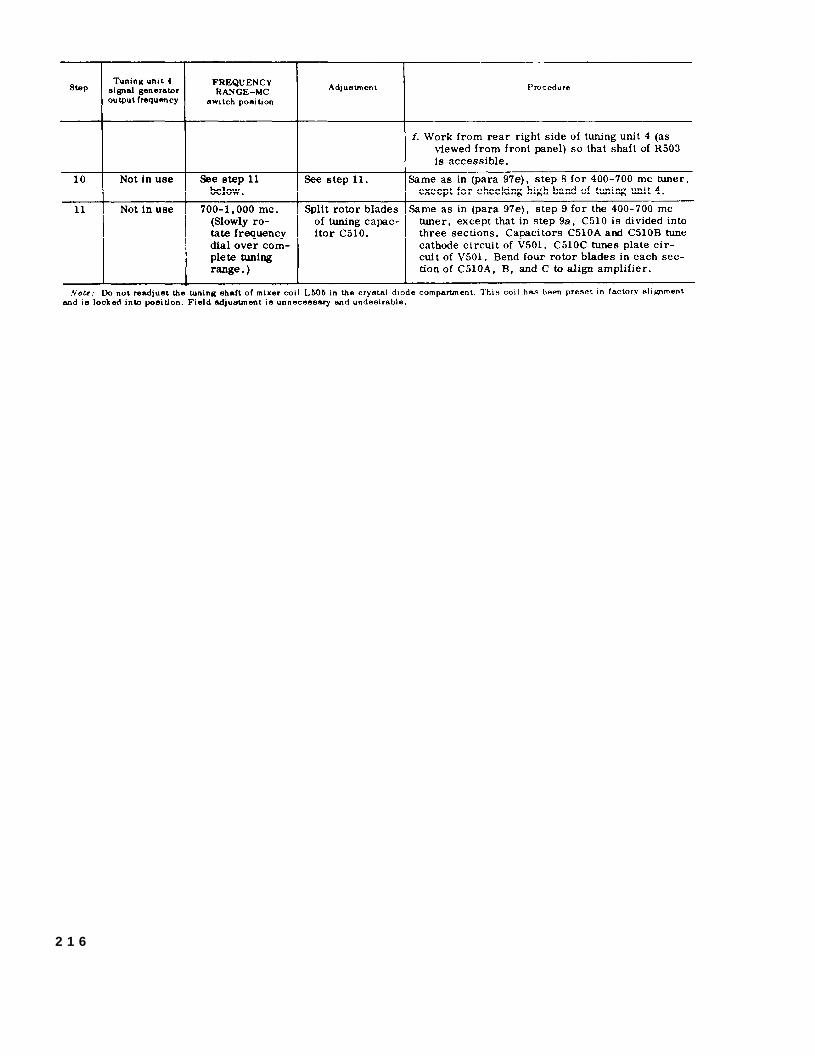
2 1 6
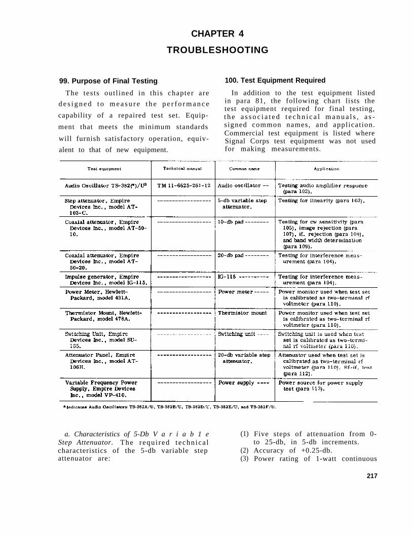
CHAPTER 4
TROUBLESHOOTING
99. Purpose of Final Testing 100. Test Equipment Required
The tests outl ined in this chapter are In addition to the test equipment listed
d e s i g n e d t o m e a s u r e t h e p e r f o r m a n c e in para 81, the following chart lists thetest equipment required for final testing,
capability of a repaired test set. Equip- t h e a s s o c i a t e d t e c h n i c a l m a n u a l s , a s -ment that meets the minimum standards signed common names, and applicat ion.
Commercial test equipment is listed wherewill furnish satisfactory operation, equiv- Signal Corps test equipment was not usedalent to that of new equipment. for making measurements.
a. Characteristics of 5-Db V a r i a b 1 e (1)Step Attenuator. The requ i red t echn ica lcharacteristics of the 5-db variable step (2)attenuator are: (3)
Five steps of attenuation from 0-to 25-db, in 5-db increments.Accuracy of +0.25-db.Power rating of 1-watt continuous
217
power or 1-kilowatt peak power.(4) Input and output impedance of 50-
ohms.(5) Voltage standing wave rat io no
grea te r than 1 .15- to l -UP to afrequency limit of l,000-mc e
(6) Coaxial series N-type connectorsat input and output terminations.
b . C h a r a c t e r i s t i c s o f 2 0 - D b V a r i a b l eStep At tenuator. The requ i red t echn ica lcharacteristics of the 20-db variable stepattenuator are the same as those l is tedin a above, except that there are five stepsof attenuation from 0- to 80-db, in 20-dbinc rements .
c. Characterist ics of 10-Db Pad. T h erequired technical characterist ics of the10-db pad are:
(1) Attenuation ratio of 10-db.(2) Accuracy of ±0.25-db.(3) Coaxial s tructure, terminated in
N-type male connector at one endand N- type female connec to r a topposite end.
(4) Power rating of l-watt continuouspower or 1-kilowatt peak power.
(5) Input and output impedance of 50-ohms .
(6) Voltage standing wave rat io nogreater than 1.15 to 1 up to afrequency limit of 2,000-mc.
d. Characterist ics of 20-Db Pad. T h erequired technical characterist ics of the20-db pad are the same as those listed inb above, except that the attenuation ratiois 20-db.
e. Characteristics of P o w e r Meter.The required technical characteristics ofthe power meter are:
(1) Power range from 10-microwattsto 10-mil l iwatts (seven ranges) .Power range also calibrated in dbmfrom -20-dbm to +10-dbm.
(2) Accuracy +3 percent of full scale onall ranges.
(3) Operat ing impedance of 100- or200-ohms, negative, for operatingwith thermistor mount.
f . C h a r a c t e r i s t i c s o f T h e r m i s t o rMount . The requ i red t echn ica l charac -teristics of the thermistor mount are:
(1) Frequency range of 10-mc to 10-kmc.
(2) SWR (standing wave ratio) of lessthan 1.5 (less than 1.3 from 50-mc to 7-kmc).
(3) Power range of 10-microwatts to10-mil l iwatts .
g. Characteristics of Power Supply. T h erequired technical characterist ics of thepower supply are:
(1) Variable frequency range of 47-to 6,000-cps in two ranges: 47-to 600-cps and 470- to 6,000-cps.
(2 ) Power ou tpu t 400-va (vo l t am-peres) continuous operation.
(3) Output voltage of 75- to 150-voltsvariable.
(4) Distortion of less than l-percentf rom 47- to 2 ,000-cps and l e s st h a n 3 - p e r c e n t f r o m 2 , 0 0 0 - t o6,000-cps.
(5) Voltage regulation of less than 2-percent from no load to fill load.
(6) Frequency accuracy of ±-percent.(7) Frequency stabil i ty of ±l/2-per-
cent after 15 minute warmup.h. Characteristics of IG-115. The re-
quired technical characteristics of the IG-115 impulse generator are:
(1) Frequency spectrum of 100-kc to1,000-mc, flat within +1/2-db.
(2) Pulse width of 0.0005-microsec-ond.
(3) Output impedance of 50-ohms.(4) Output level (peak) of 100,000 -
microvolts per megacycle band-width, adjustable over a 100-dbrange by means of step attenuatorsin l-db steps.
(5) Pulse polarity reversible.(6) Repetition rate of 50- to 60-cps
(line frequency).i . Characteris t ics of Switching Unit .
The requ i red charac te r i s t i c s o f t h eswitching unit are:
(1) Coaxial type switch construction.(2) Frequency limit up to 1,000-mc.
j. Additional Items Required for FinalTesting.
(1) Resistor, 600-ohm, l/2-watt.(2) Potentiometer, 250,000-ohm.(3) Cable, Radio Frequency RG-5B/U
(or RG-212/U).(4) Connector, Plug, Electrical UG-
18 D/U (two each).
218
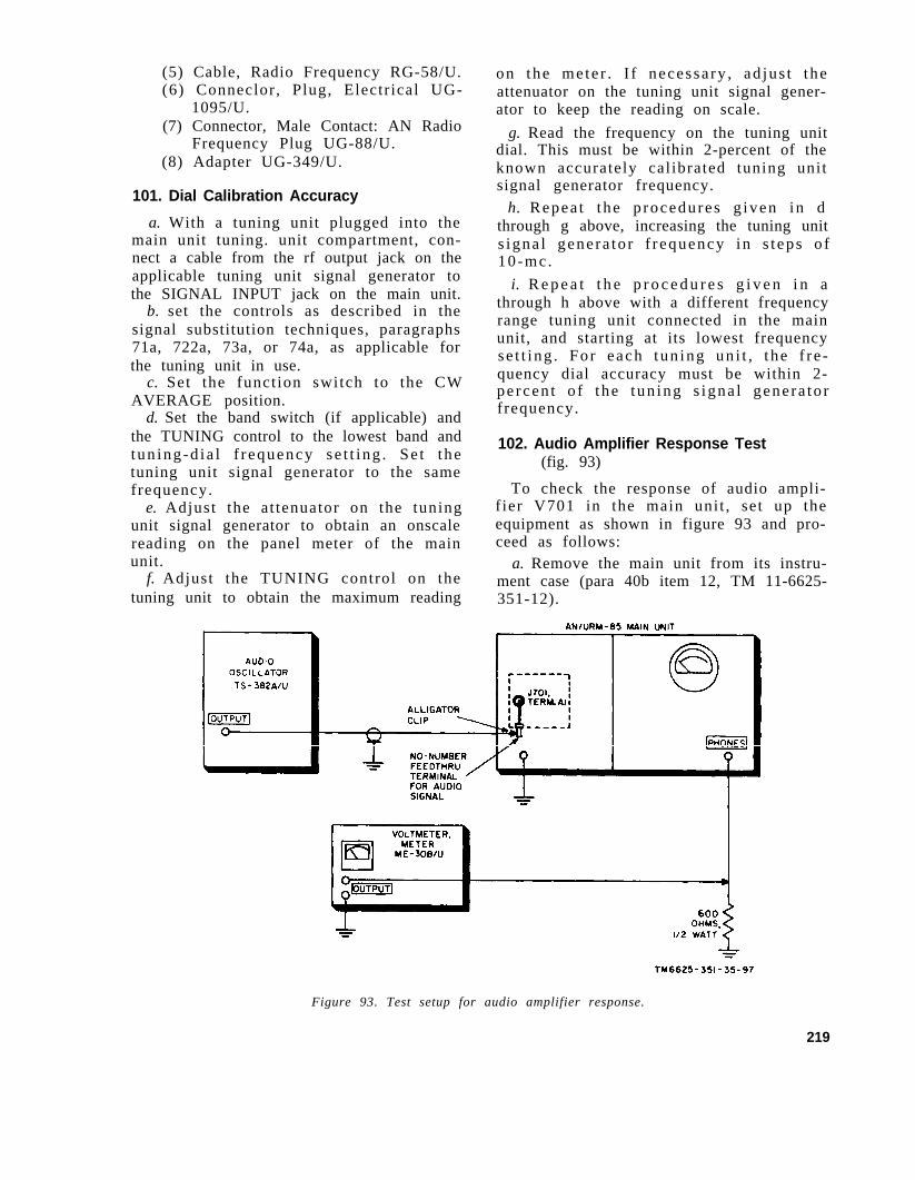
(5) Cable, Radio Frequency RG-58/U.(6) Conneclor, Plug, Electrical UG-
1095/U.(7) Connector, Male Contact: AN Radio
Frequency Plug UG-88/U.(8) Adapter UG-349/U.
101. Dial Calibration Accuracy
a. With a tuning unit plugged into themain unit tuning. unit compartment, con-nect a cable from the rf output jack on theapplicable tuning unit signal generator tothe SIGNAL INPUT jack on the main unit.
b. set the controls as described in thesignal substitution techniques, paragraphs71a, 722a, 73a, or 74a, as applicable forthe tuning unit in use.
c. Set the function switch to the CWAVERAGE position.
d. Set the band switch (if applicable) andthe TUNING control to the lowest band andtun ing-d ia l f r equency se t t ing . Se t thetuning unit signal generator to the samefrequency.
e. Adjust the at tenuator on the tuningunit signal generator to obtain an onscalereading on the panel meter of the mainunit.
f. Adjust the TUNING control on thetuning unit to obtain the maximum reading
on the mete r . I f necessa ry , ad jus t theattenuator on the tuning unit signal gener-ator to keep the reading on scale.
g. Read the frequency on the tuning unitdial. This must be within 2-percent of theknown accurately calibrated tuning unitsignal generator frequency.
h. Repea t the p rocedures g iven in dthrough g above, increasing the tuning units igna l gene ra to r f r equency in s t eps o f10-mc .
i. R e p e a t t h e p r o c e d u r e s g i v e n i n athrough h above with a different frequencyrange tuning unit connected in the mainunit, and starting at its lowest frequencyse t t ing . For each tun ing un i t , t he f r e -quency dial accuracy must be within 2-pe rcen t o f the tun ing s igna l gene ra to rfrequency.
102. Audio Amplifier Response Test(fig. 93)
To check the response of audio ampli-f ier V701 in the main unit , set up theequipment as shown in figure 93 and pro-ceed as follows:
a. Remove the main unit from its instru-ment case (para 40b item 12, TM 11-6625-351-12).
Figure 93. Test setup for audio amplifier response.
219
b. Connect the output of the audio oscil-lator (para 100) to the input of audio am-plifier V701A in the main unit of the testset. A convenient point for injecting theaudio oscillator signal is at the unnum-bered feedthrough terminal at the bottomright corner of the f i l ter box assembly(fig. 45). This terminal is essentially thesame circuit point as terminal Al of con-nector J701.
c. Connect Voltmeter, Meter ME-30B/U across a 600-ohm, l /2-watt resistor ,connec ted f rom PHONES jack J702 tochassis ground.
d. Adjust the output of the audio oscil-lator to produce a signal of O l-volt am-plitude from terminal Al of J701 to ground.
e. Tune the audio oscillator to 1,000 -cps and record the voltage indication shownon the ME-30B/U.
f. Repeat procedure e above at the testfrequencies of 150, 500, 2,000, 3,000,4,000, and 5,000-cps. Note the voltagereading at each test frequency. The audioresponse curve must be flat, within 8-dbof the 1,000-cycle value, with a gradualslope-off at each end. There must be noresonant peaks.
103. Linearity Test(fig, 94)
Two tes t s a re r equ i red to check thelinearity of the test set; one checks thelinearity in the PULSE PEAK position ofthe function switch, and the other checksthe linearity in the CW AVERAGE posi-tion of the function switch. Remove themain unit from its instrument case (para 40b, item 12, TM 11-6625-351-12). Set up theequipment as shown in figure 94 and pro-ceed as follows:
a. Pulse Peak Test. Connect the appli-cable tuning unit s ignal generator (de-pending on the tuning under test) througha 5-db variable step attenuator (para 100),or equivalent, and through the RG-5B/Ucable, to the SIGNAL INPUT jack of thetest set.
(1) Set the main unit function switch tothe PULSE PEAK position.
(2) Set the tuning unit signal generatoroutput level control to produce a
220
(3)
(4)
(5)
(6)
1,000- or 10,000-microvolt signal(as required) at the SIGNAL IN-PUT jack (any frequency).Set the variable 5-db step atten-uator to the 25-db position.Rotate the SIGNAL ATTENUATORDB switch to 60 and adjust theGAIN control on the tuning unit toproduce a 0-db indication on themain unit panel meter.Decrease the set t ing of the 5-dbvar i ab le s t ep a t t enua to r in foursteps, from 25- to 5-db, and recordthe corresponding indication of theAN/URM-85 panel meter.Check the panel meter for a 5-db±1 increase for each step decreaseo f t h e 5 - d b v a r i a b l e s t e p a t -tenuator .
b. CW AVERAGE Test. This test is de-signed to check the test set for linearitywhen a 100-percent modulated cw signalis received at the SIGNAL INPUT jack.Signal sources capable of producing sucha signal are not readily available. Thefollowing test procedures, when used withan unmodulated cw source, will simulatethe conditions above. For this test, changethe setting of the function switch to the CWAVERAGE position.
(1)
(2)
(3)
(4)
Set the tuning unit signal gener-ator output level control to pro-d u c e a 2,000-microvolt, or a20,000 -microvolt s ignal (as re-quired) at the SIGNAL INPUT jack.Set the frequency of the tuning unitsignal generator and the frequencydial of the tuning unit under test toa frequency at the high end of theband under test.Adjust the GAIN control on thet u n i n g u n i t t o p r o d u c e a f u l l -scale, 20-db indication on the mainunit panel meter with the variable5-db step attenuator set to the 5-db position.P l a c e t h e I F . C A T H O D E F O L -LOWER ADJ switch S704, a chassisadjustment control (fig. 51) in itsopen-circuit position (check witha multimeter). Shunt its terminalswith a 250,000-ohm potentiometer.Use alligator clips to connect one
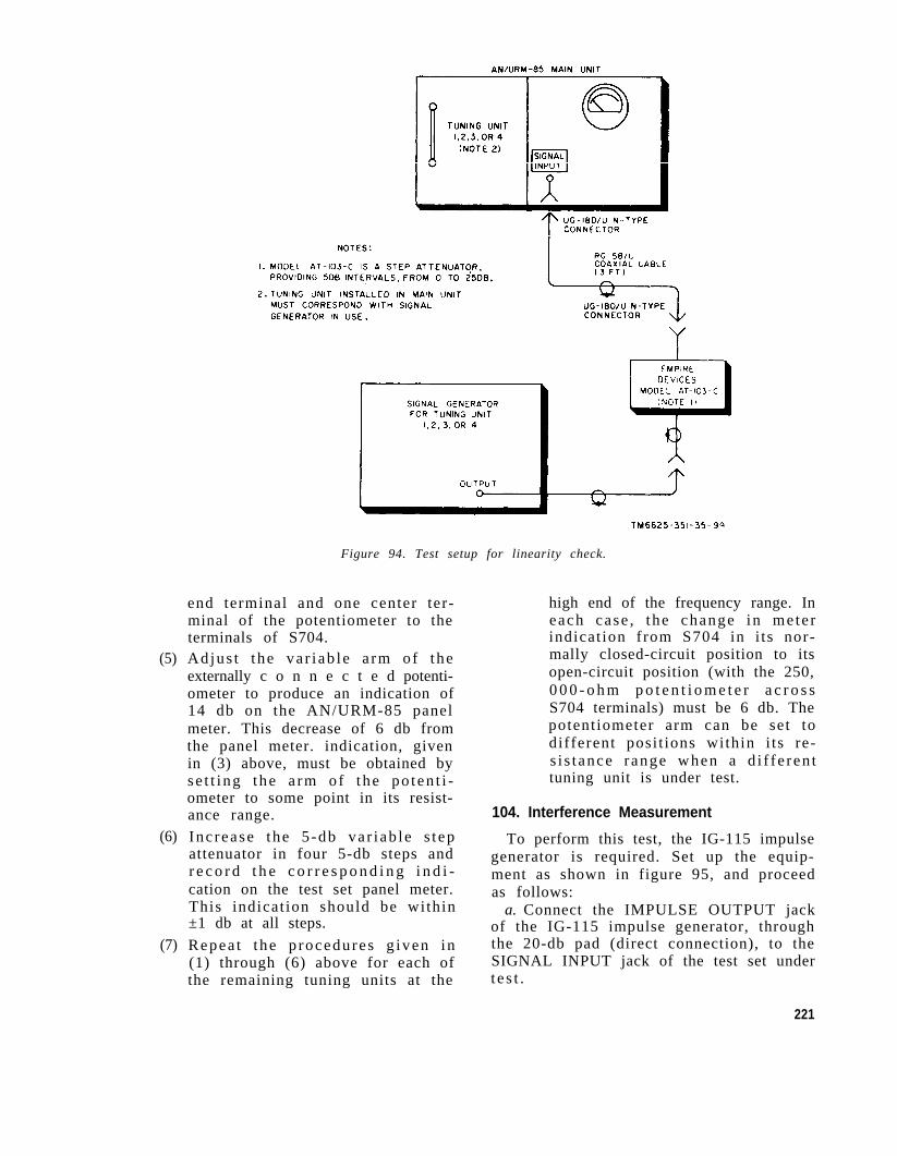
(5)
(6)
(7)
Figure 94. Test setup for linearity check.
end terminal and one center ter-minal of the potentiometer to theterminals of S704.Adjus t the va r i ab le a rm of theexternally c o n n e c t e d potenti-ometer to produce an indication of14 db on the AN/URM-85 panelmeter. This decrease of 6 db fromthe panel meter. indication, givenin (3) above, must be obtained byse t t ing the a rm o f the po ten t i -ometer to some point in its resist-ance range.
Inc rease the 5 -db va r i ab le s t epattenuator in four 5-db steps andr e c o r d t h e c o r r e s p o n d i n g i n d i -cation on the test set panel meter.This indicat ion should be within±1 db at all steps.
Repea t the p rocedures g iven in(1) through (6) above for each ofthe remaining tuning units at the
high end of the frequency range. Ineach case , the change in mete rindicat ion from S704 in i ts nor-mally closed-circuit position to itsopen-circuit position (with the 250,0 0 0 - o h m p o t e n t i o m e t e r a c r o s sS704 terminals) must be 6 db. Thepotentiometer arm can be set todifferent posi t ions within i ts re-s i s t ance range when a d i f fe ren ttuning unit is under test.
104. Interference Measurement
To perform this test, the IG-115 impulsegenerator is required. Set up the equip-ment as shown in figure 95, and proceedas follows:
a. Connect the IMPULSE OUTPUT jackof the IG-115 impulse generator, throughthe 20-db pad (direct connection), to theSIGNAL INPUT jack of the test set undert e s t .
221
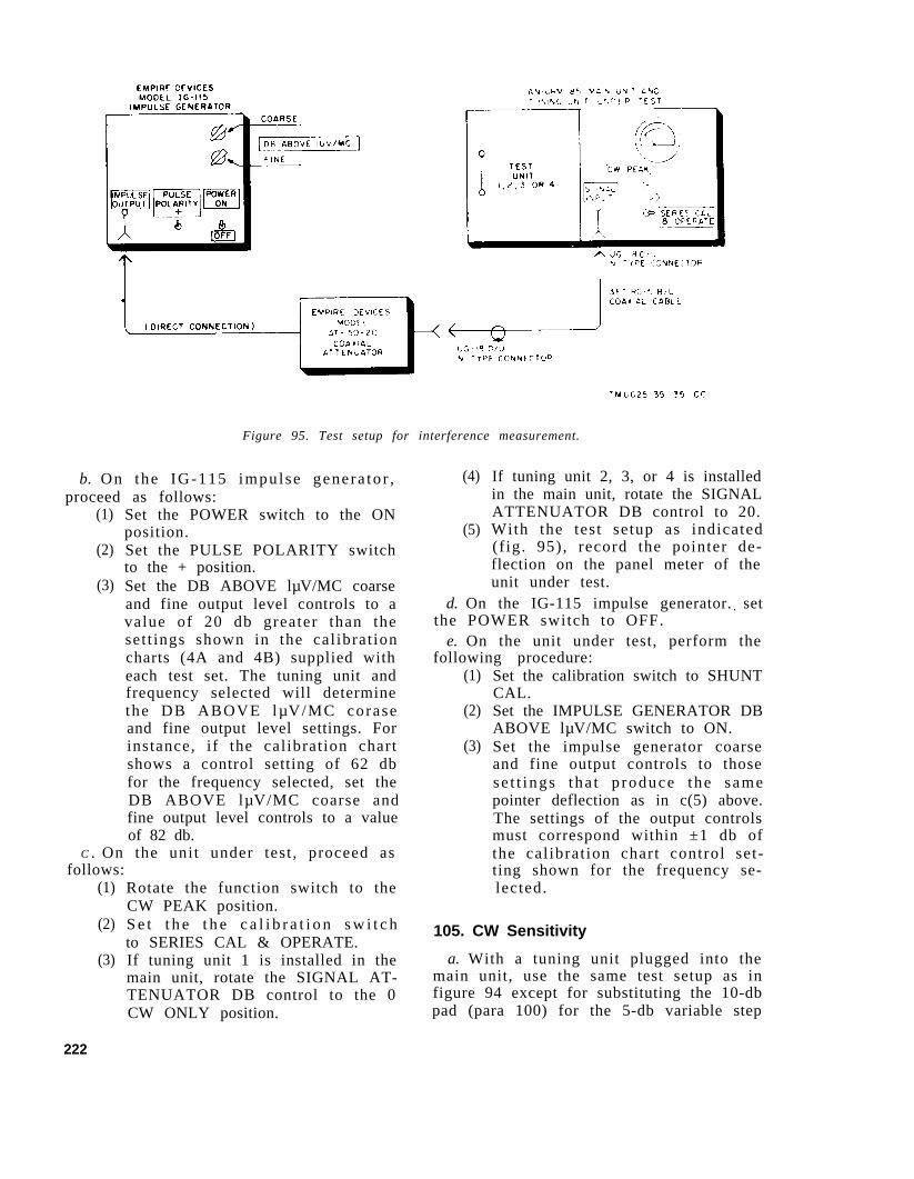
Figure 95. Test setup for interference measurement.
b. On the IG-115 impulse genera to r ,proceed as follows:
(1)
(2)
(3)
Set the POWER switch to the ONposition.Set the PULSE POLARITY switchto the + position.Set the DB ABOVE lµV/MC coarseand fine output level controls to avalue of 20 db greater than theset t ings shown in the cal ibrat ioncharts (4A and 4B) supplied witheach test set. The tuning unit andfrequency selected will determinethe DB ABOVE lµV/MC coraseand fine output level settings. Forinstance, if the calibration chartshows a control setting of 62 dbfor the frequency selected, set theDB ABOVE lµV/MC coarse andfine output level controls to a valueof 82 db.
C . On the unit under test , proceed asfollows:
(1)
(2)
(3)
222
Rotate the function switch to theCW PEAK position.S e t t h e t h e c a l i b r a t i o n s w i t c hto SERIES CAL & OPERATE.If tuning unit 1 is installed in themain unit, rotate the SIGNAL AT-TENUATOR DB control to the 0CW ONLY position.
(4)
(5)
If tuning unit 2, 3, or 4 is installedin the main unit, rotate the SIGNALATTENUATOR DB control to 20.With the test setup as indicated(fig. 95), record the pointer de-flection on the panel meter of theunit under test.
d. On the IG-115 impulse generator. setthe POWER switch to OFF.
.
e. On the unit under test, perform thefollowing procedure:
(1)
(2)
(3)
Set the calibration switch to SHUNTCAL.Set the IMPULSE GENERATOR DBABOVE lµV/MC switch to ON.Set the impulse generator coarseand fine output controls to thosese t t ings tha t p roduce the samepointer deflection as in c(5) above.The settings of the output controlsmust correspond within ±1 db ofthe cal ibrat ion chart control set-ting shown for the frequency se-lected.
105. CW Sensitivity
a. With a tuning unit plugged into themain unit, use the same test setup as infigure 94 except for substituting the 10-dbpad (para 100) for the 5-db variable step
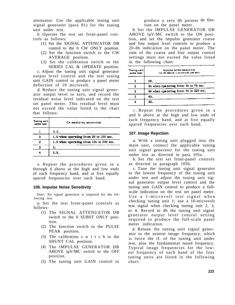
attenuator. Use the applicable tuning unitsignal generator (para 81) for the tuningunit under test.
b. Operate the test set front-panel con-trols as follows:
(1) Set the SIGNAL ATTENUATOR DBcontrol to the 0 CW ONLY position.
(2) Set the function switch to the CWAVERAGE position.
(3) Set the calibration switch to theSERIES CAL & OPERATE position.
c. Adjust the tuning unit signal generatoroutput level control and the test tuningunit GAIN control to produce a panel meterdeflection of 10 microvolt.
d. Reduce the tuning unit signal gener-ator output level to zero, and record theresidual noise level indicated on the testset panel meter. This residual level mustnot exceed the value listed in the chartthat follows:
e. Repea t the p rocedures g iven in athrough d above at the high and low endsof each frequency band, and at five equallyspaced frequencies over each band.
106. Impulse Noise Sensitivity
Note: No signal generator is required for the fol-lowing test.
a. Set the test front-panel controls asfollows:
(1)
(2)
(3)
(4)
(5)
The SIGNAL ATTENUATOR DBswitch to the 0 SUBST ONLY posi-tion.The function switch to the PULSEPEAK position.The calibration s w i t c h to theSHUNT CAL position.The IMPULSE GENERATOR DBABOVE lµV/MC switch to the OFFposition.The tuning unit GAIN control to
produce a zero db pointertion on the panel meter.
de flee-
b. Set the IMPULSE GENERATOR DBABOVE lµV/MC switch to the ON posi-tion, and set the impulse generator coarseand fine output level controls to produce a20-db indication on the panel meter. Thesum of the coarse and fine output controlsettings must not exceed the value listedin the following chart:
C . Repea t the p rocedures g iven in aand b above at the high and low ends ofeach frequency band, and at five equallyspaced frequencies over each band.
107. Image Rejection
a. With a tuning unit plugged into themain unit, connect the applicable tuningunit signal generator for the tuning unitunder test as directed in para 105a.
b. Set the test set front-panel controlsas directed in paragraph 105b.
c. Tune the tuning unit signal generatorto the lowest frequency of the tuning unitunder test and adjust the tuning unit sig-nal generator output level control and thetuning unit GAIN control to produce a full-scale indication on the test set panel meter.U s e a 1 - m i c r o v o l t t e s t s i g n a l w h e nchecking tuning unit 1; use a 10-microvolttest signal when checking tuning unit 2, 3,or 4. Record in db the tuning unit signalgene ra to r ou tpu t l eve l con t ro l s e t t i ngrequired to produce the full-scale panelmeter indication.
d. Retune the tuning unit signal gener-ator to the nearest image frequency, whichis twice the if. of the tuning unit undertest, plus the fundamental tuned frequency.Typical image frequencies for the low-est frequency of each band of the fourtuning units are l is ted in the fol lowingchart:
223
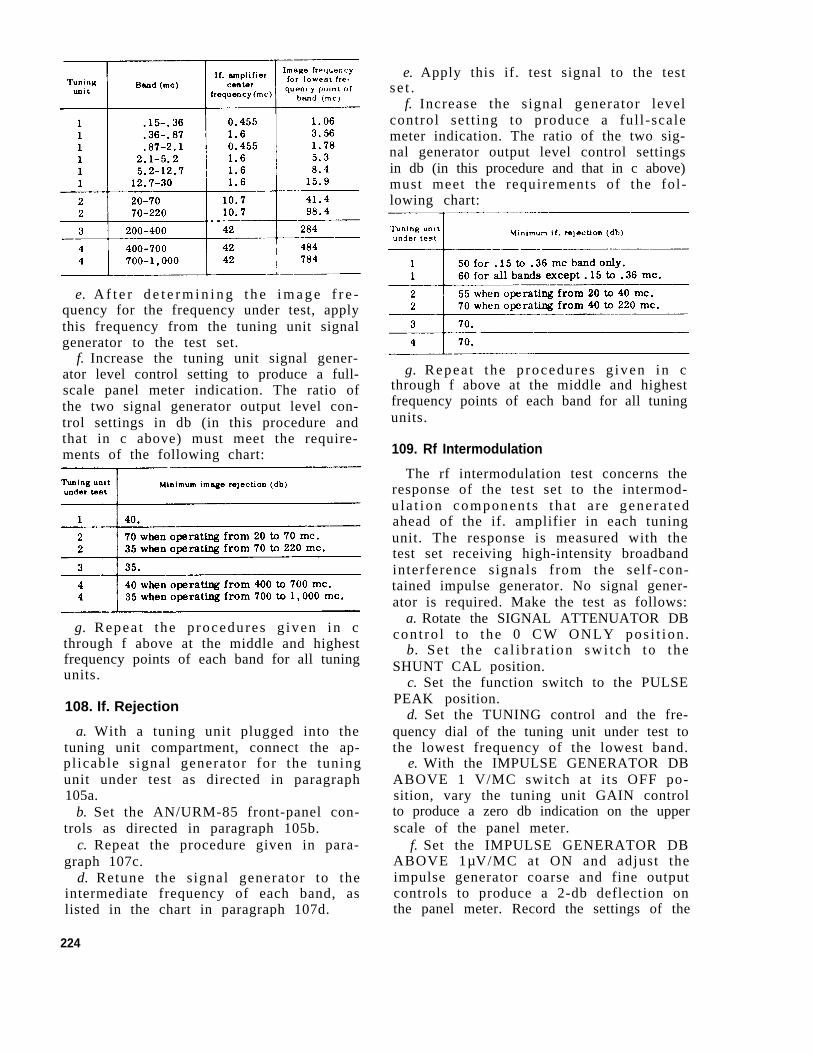
e. A f t e r d e t e r m i n i n g t h e i m a g e f r e -quency for the frequency under test, applythis frequency from the tuning unit signalgenerator to the test set.
f. Increase the tuning unit signal gener-ator level control setting to produce a full-scale panel meter indication. The ratio ofthe two signal generator output level con-trol settings in db (in this procedure andthat in c above) must meet the require-ments of the following chart:
g. Repea t the p rocedures g iven in cthrough f above at the middle and highestfrequency points of each band for all tuningunits.
108. If. Rejection
a. With a tuning unit plugged into thetuning unit compartment, connect the ap-pl icable s ignal generator for the tuningunit under test as directed in paragraph105a.
b. Set the AN/URM-85 front-panel con-trols as directed in paragraph 105b.
c. Repeat the procedure given in para-graph 107c.
d. Retune the signal generator to theintermediate frequency of each band, aslisted in the chart in paragraph 107d.
e. Apply this if. test signal to the testse t .
f. Increase the signal generator levelcontrol set t ing to produce a ful l-scalemeter indication. The ratio of the two sig-nal generator output level control settingsin db (in this procedure and that in c above)must meet the requirements of the fol-lowing chart:
g. Repea t the p rocedures g iven in cthrough f above at the middle and highestfrequency points of each band for all tuningunits.
109. Rf Intermodulation
The rf intermodulation test concerns theresponse of the test set to the intermod-u la t ion componen t s tha t a re genera tedahead of the if. amplifier in each tuningunit. The response is measured with thetest set receiving high-intensity broadbandinterference signals from the self-con-tained impulse generator. No signal gener-ator is required. Make the test as follows:
a. Rotate the SIGNAL ATTENUATOR DBcont ro l to the 0 CW ONLY pos i t ion .
b. Se t the ca l ib ra t ion swi tch to theSHUNT CAL position.
c. Set the function switch to the PULSEPEAK position.
d. Set the TUNING control and the fre-quency dial of the tuning unit under test tothe lowest frequency of the lowest band.
e. With the IMPULSE GENERATOR DBABOVE 1 V/MC switch at i ts OFF po-sition, vary the tuning unit GAIN controlto produce a zero db indication on the upperscale of the panel meter.
f. Set the IMPULSE GENERATOR DBABOVE 1µV/MC at ON and adjust theimpulse generator coarse and fine outputcontrols to produce a 2-db deflection onthe panel meter. Record the settings of the
224
impulsethe sum
generator output level controls;of the settings is the reference—
sensitivity.g. Now disable the local oscillator in the
tuning unit under test. Each tuning unit re-quires a different procedure for this oper-ation. Perform the procedure outlined inthe following chart:
h. With the local oscillator of the tuningunit disabled (g above), readjust the im-pulse generator coarse and fine outputlevel control settings to again produce a2-db indication on the panel meter. Recordthe sum of the two output level controlsett ings: this is the rf intermodulat ionsensi t ivi ty .
i. Subt rac t the va lue o f the r f in t e r -modulation sensitivity (h above) from thereference sensi t ivi ty (f above) to deter-mine the difference in db. This differencein settings for the impulse generator out-put level controls must be the same orhigher than the values shown in the fol-lowing chart:
j. R e p e a t t h e p r o c e d u r e g i v e n i n ethrough i above for the high-frequency end
of the band under test; then check at twoo the r equa l ly spaced f r equency po in t swithin the band.
k. Repeat the procedures in e throughj for each band of the tuning unit under test.
110. Calibration as Two-Terminal RFVoltmeter
This procedure is used to calibrate. thetest set as a two-terminal rf voltmeter .Set up the equipment as shown in figure94; however, use the 10-db pad instead ofthe 5-db variable step attenuator. The 10-db pad can be connected directly to thetuning unit signal generator.
a. If tuning units 1, 2, or 3, are used,connect the applicable tuning unit signalgenerator (recently cal ibrated for poweroutput) to the test set and proceed asfollows:
(1)
(2)
(3)
(4)
(5)
(6)
(7)
Se t the func t ion swi tch to CWAVERAGE a n d the calibrations w i t c h t o S E R I E S C A L & O P -ERATE.If tuning unit 1 is used, set theSIGNAL ATTENUATOR switch to0 CW ONLY; if tuning units 2 or3 are used set the SIGNAL AT-TENUATOR switch to 20 DB.Set the tuning unit signal generatoro u t p u t l e v e l t o p r o d u c e a 1 0 -microvolt s ignal at the SIGNALINPUT terminal of the test set fortuning unit 1, or a 100 microvoltsignal for tuning units 2 or 3.
Note: If the 10-db pad is too large toprovide a signal of proper amplitude atthe test set SIGNAL INPUT terminal, usea Pad of a smaller value (AT-50-8) to pro-duce the proper signal amplitude.
Adjust the GAIN control to obtaina 20-db reading on the test setpanel meter.Se t the func t ion swi tch to CWPEAK and the calibrat ion switchto SHUNT CAL.Set the IMPULSE GENERATOR DBA B O V E l µ V / M C s w i t c h t o O Nand adjust the impulse generatoroutput controls (coarse and fine) toagain obtain a 20-db reading on thetest set panel meter.Record the settings of the impulse
225
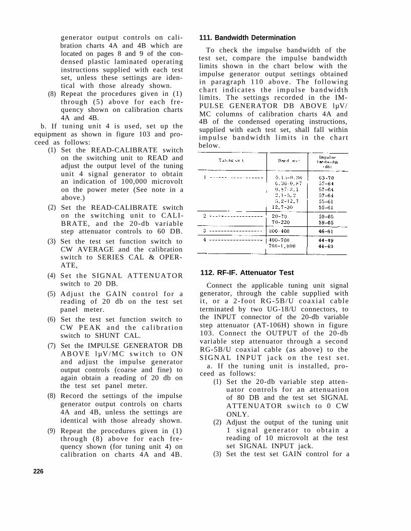
(8)
b. If
generator output controls on cali-bration charts 4A and 4B which arelocated on pages 8 and 9 of the con-densed plastic laminated operatinginstructions supplied with each testset, unless these settings are iden-tical with those already shown.Repeat the procedures given in (1)through (5) above for each fre-quency shown on calibration charts4A and 4B.tuning unit 4 is used, set up the
equipment as shown in figure 103 and pro-ceed as follows:
(1)
(2)
(3)
(4)
(5)
(6)
(7)
(8)
(9)
Set the READ-CALIBRATE switchon the switching unit to READ andadjust the output level of the tuningunit 4 signal generator to obtainan indication of 100,000 microvolton the power meter (See note in aabove.)Set the READ-CALIBRATE switchon the switching unit to CALI-BRATE, and the 20-db variablestep attenuator controls to 60 DB.
Set the test set function switch toCW AVERAGE and the calibrationswitch to SERIES CAL & OPER-ATE,
Set the SIGNAL ATTENUATORswitch to 20 DB.
Adjus t the GAIN con t ro l fo r areading of 20 db on the test setpanel meter.Set the test set function switch toC W P E A K a n d t h e c a l i b r a t i o nswitch to SHUNT CAL.
Set the IMPULSE GENERATOR DBA B O V E l µ V / M C s w i t c h t o O Nand adjust the impulse generatoroutput controls (coarse and fine) toagain obtain a reading of 20 db onthe test set panel meter.
Record the settings of the impulsegenerator output controls on charts4A and 4B, unless the settings areidentical with those already shown.
Repeat the procedures given in (1)through (8) above for each fre-quency shown (for tuning unit 4) oncalibration on charts 4A and 4B.
111. Bandwidth Determination
To check the impulse bandwidth of thetest set, compare the impulse bandwidthlimits shown in the chart below with theimpulse generator output settings obtainedin paragraph 110 above. The fol lowingchar t i nd ica te s the impul se bandwid thlimits. The settings recorded in the IM-PULSE GENERATOR DB ABOVE lµV/MC columns of calibration charts 4A and4B of the condensed operating instructions,supplied with each test set, shall fall withinimpul se bandwid th l imi t s in the cha r tbelow.
112. RF-IF. Attenuator Test
Connect the applicable tuning unit signalgenerator, through the cable supplied withi t , o r a 2 - foo t RG-5B/U coax ia l cab leterminated by two UG-18/U connectors, tothe INPUT connector of the 20-db variablestep attenuator (AT-106H) shown in figure103. Connect the OUTPUT of the 20-dbvariable step attenuator through a secondRG-5B/U coaxial cable (as above) to theS I G N A L I N P U T j a c k o n t h e t e s t s e t .
a. If the tuning unit is installed, pro-ceed as follows:
(1)
(2)
(3)
Set the 20-db variable step atten-uator controls for an at tenuationof 80 DB and the test set SIGNALATTENUATOR swi tch to 0 CWONLY.Adjust the output of the tuning unit1 s igna l gene ra to r to ob ta in areading of 10 microvolt at the testset SIGNAL INPUT jack.Set the test set GAIN control for a
226
(4)
(5)
(6)
full-scale indication on the panelm e t e r .Increase the test set SIGNAL AT-TENUATOR switch setting by 20 dband decrease the 20-db variablestep attenuator controls by 20 db.The reading on the test set panelm e t e r s h o u l d r e m a i n c o n s t a n t ,within ±2O percent for each 20-dbchange in control settings.Repeat the procedure given in (4)above fo r each pos i t ion o f theSIGNAL ATTENUATOR switch Upto the 80 DB position.Repeat the procedures given in (1)t h r o u g h ( 4 ) a b o v e a t t h e l o w ,middle, and high end of each bandon the tuning unit.
b. If tuning units 2, 3, or 4 are installed,proceed as follows:
(1)
(2)
Set the 20-db variable step atten-uator controls for an at tenuationof 60 DB and the test set SIGNALATTENUATOR switch to 20 DB.Adjust the output of the tuning units igna l gene ra to r to ob ta in 100microvolt at the test set SIGNALINPUT jack.
227
(3)
(4)
(5)
Set the test set GAIN control for afill-scale indication on the panelm e t e r .Set the test set SIGNAL ATTEN-UATOR switch to 0 CW ONLY andthe 20-db variable step attenuatorfor an attenuation of 80 DB.Repeat the procedures given in a(4), (5), and (6) of a above.
113. Power Supply Test
a. C o n n e c t t h e t e s t s e t t h r o u g h t h eisolation transformer (TF-248/G) to thepower supply (VP-410), and perform asmany of the final tests as are necessaryto verify that the test set operates prop-erly at each of the following frequenciesand input voltages:
Frequencies Input voltages50 cps 100, 117, and 130 vac
60 cps 100, 117, and 130 vac
400 cps 100, 117, and 130 vacb. Per fo rm the f ina l t e s t s de te rmined
in a above with an input of 230 vac at afrequency of 60 cps.
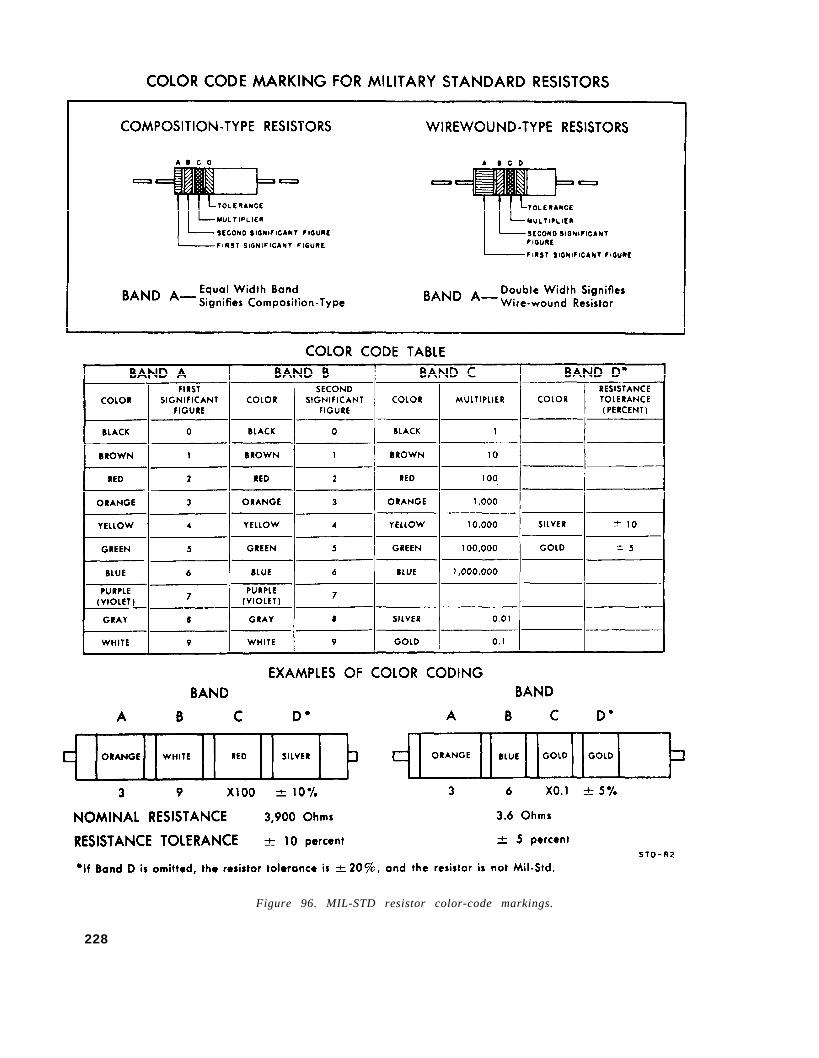
Figure 96. MIL-STD resistor color-code markings.
228
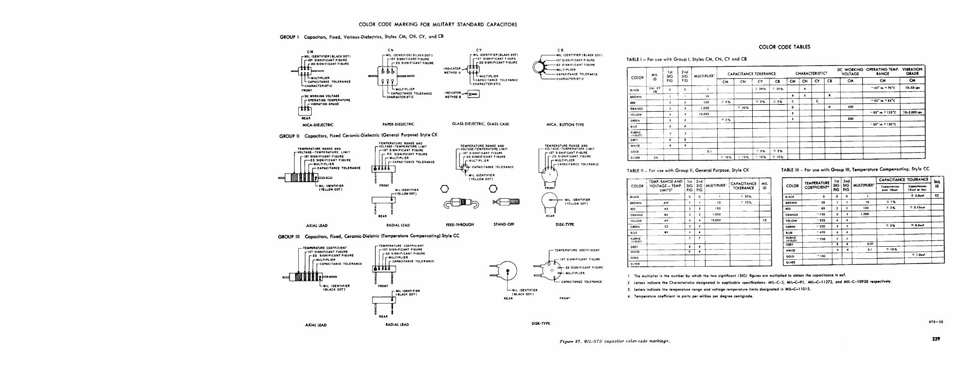
APPENDIX
REFERENCES
Following is a list of references applicable and available to the field and depot mainte-nance repairman of Radio Interference Measuring Set AN/URM-85.
DA Pamphlet 310-4
TB SIG 225TM 11-1242
TM 11-5030ATM 11-5527TM 11-5551-DTM 11-6625-200-12
TM 11-6625-261-12
TM 11-6625-274-12
TM 11-6625-280-15
TM 11-6625-316-12
TM 11-6625-320-12
TM 11-6625-351-12
TM 11-6625-351-20P
TM 11-6625-351-35P
Index of Technical Manuals, Technical Bulletins, Supply Bul-letins, Lubrication Orders, and Modification Work Orders.
Radioactive Electron Tube Handling.Crystal Rectifier Test Sets TS-268/U, TS-268A/U, TS-
268B/U, TS-268C/U, TS-268D/U, and TS-268E/U.Signal Generators TS-497B/URR and TS-497C/URR.Multimeters TS-352/U, TS-352A/U, and TS-352B/U.R.F. Signal Generator Set AN/URM-25D.Operation and Organizational Maintenance: Multimeter ME-
26B/U.Operator’s and Organizational Maintenance Manual: Audio
Oscillators TS-382A/U, TS-382B/U, TS-382D/U, TS-382E/U, and TS-382F/U.
operator’s and Organizational Maintenance Manual: TestSets, Electron Tube TV-7/U, TV-7A/U, TV-7B/U, and TV-7D\U.
Organizational, Field and Depot Maintenance Manual: SignalGenerators AN/URM-49, AN/URM-49A, AN/URM-49B,and AN/URM-49C.
Operator and Organizational Maintenance Manual: Test Sets,Electron Tube TV-2/U, TV-2A/U, and TV-2B/U.
Operator’s and Organizational Maintenance Manual: Volt-meter, Meter ME-30A/U and Voltmeters, Electronic ME-30B/U and ME-30C/U.
Operator and Organizational Maintenance Manual: Radio In-terference Measuring Set AN/URM-85.
Organizational Maintenance Repair Parts and Special ToolsList: Radio Interference Measuring Set AN/URM-85.
Field and Depot Repair Parts and Special Tools List for In-terference Measuring Set AN/URM-85.
231
INDEX
82a
82b
8 282c
84-8687
88-8991
92,9394
95-9798
60e1433
9
108
13
115
450a
25344250
61d
61c
61e67a6 6
53b51b
24
66b
76
6a6b
59b
191
191
1911 9 1
192-193194
197200
202,2032 0 4
208-2092 1 3
8 61 6
47
910
11
111114
117
67135475969
88
88
88107106
7771
33
106
16682
7659d
7 659e
60c
60d
60b
60g
60h
42c,45
52d,54
1819
6968
25j
6a
60a
32d32c
65b
8 3
102111
110105101108106104103113
9910911210016a65a
1819222120
1668 3
16685
86
86
85
87
87
59,63
75,78
2325
152152
35
9
85
4644
93
191
219226
225222219224223221220227217224226217
2193
2325292625
232
4857
40b40 c40d30b30c29b29c
2731
4655
3928
28a
23c23b
23a3d
7
69b
64c
76e59a
66c
1717a
32
2212c
59b
59d
59e59a
59c
60e
60c
60d
60b
6780
57575842424242
3944
6479
544141
3232
315
10
152
91
17281
106
2222
44
2914
82
83
8581
83
86
86
86
85
60g
60h
60a
60f
61d
61c
614
6 1b
61a
61b
26d36b38b
4452c54c
7575b75c
53a51a
13e13f13c13d13g
24d,
24f24c24g24a24a24h24b
23
24
4 2 d50b
61a
59c
87
87
85
87
88
88
88
88
87
88
395153627578
164165165
7671
1515141415
34
34333533333533
31
33
5971
87
83
233
e
60f
923c
28c28b28e
23a
76d
76b
76c76a76e
77d
77b
77c77a
26
64b(2)
64b(1)
24a
24b
32e5b
82a81a82b
4a
70b70
86
1132
414141
31
168
166
167166172
175
172
175172
48,51
5237
91
91
33
33
467
191190191
6
154154
6b1-5
90a90b
10065
102109105100108107106104103
9911069a
62
67c67b64a
6367a64c64b
4c71
71b71a7 lc
7272a72b72c
7373a73b73C
7474a74b74c
82c
23b
66a
102-7
199199
21793
219224222217224223223221220217225152
89
107107
9191
1079191
7155
155155156158158159159160160160161162162162163
191
32
106
35,36
37,38
234
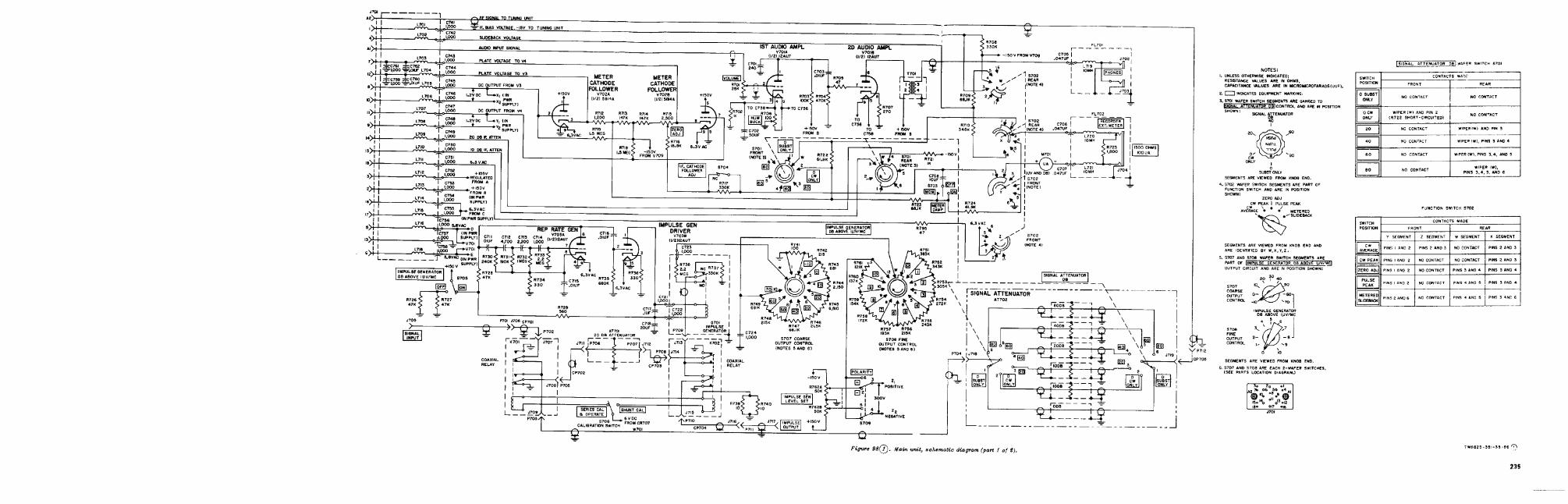
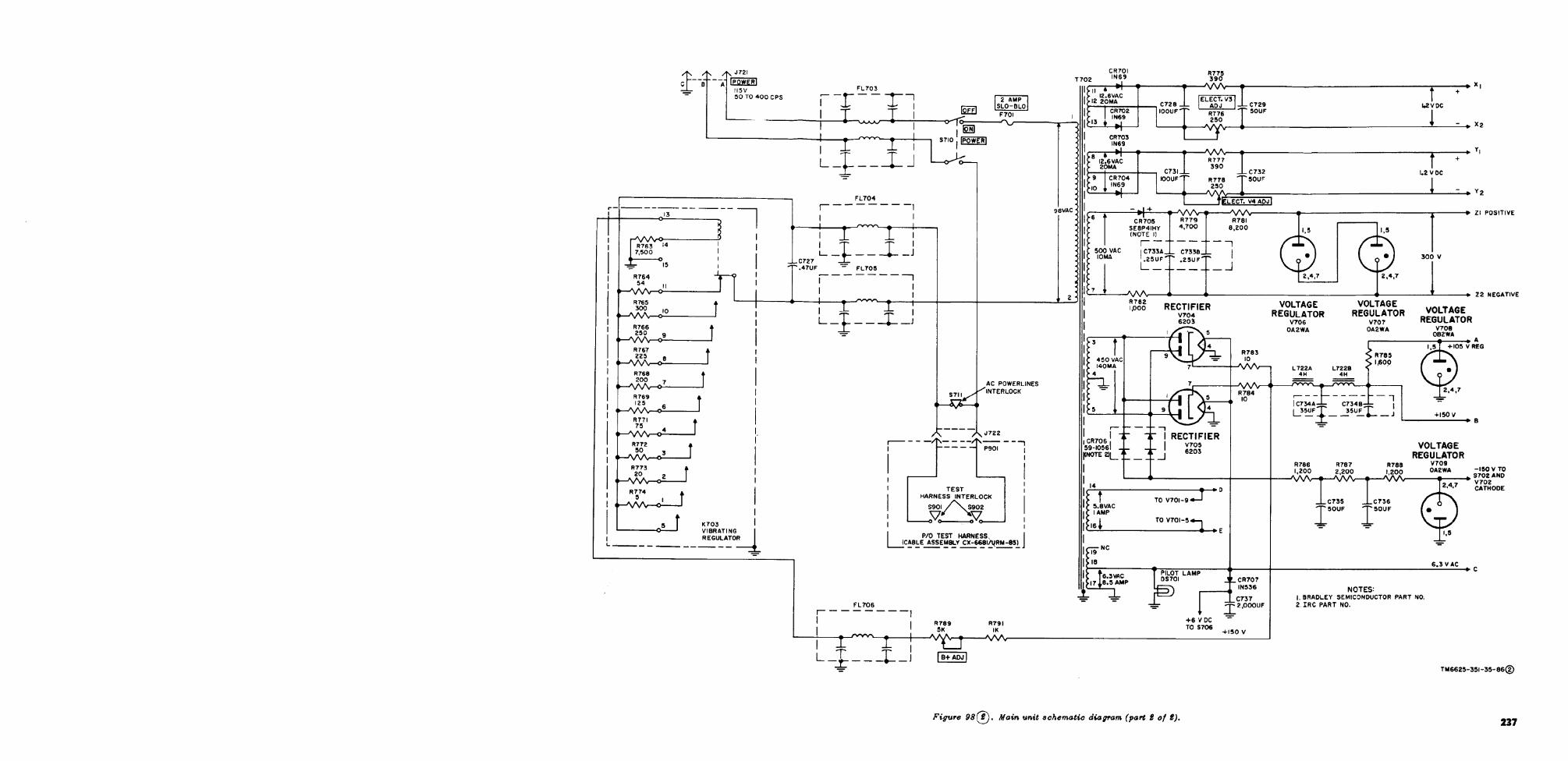
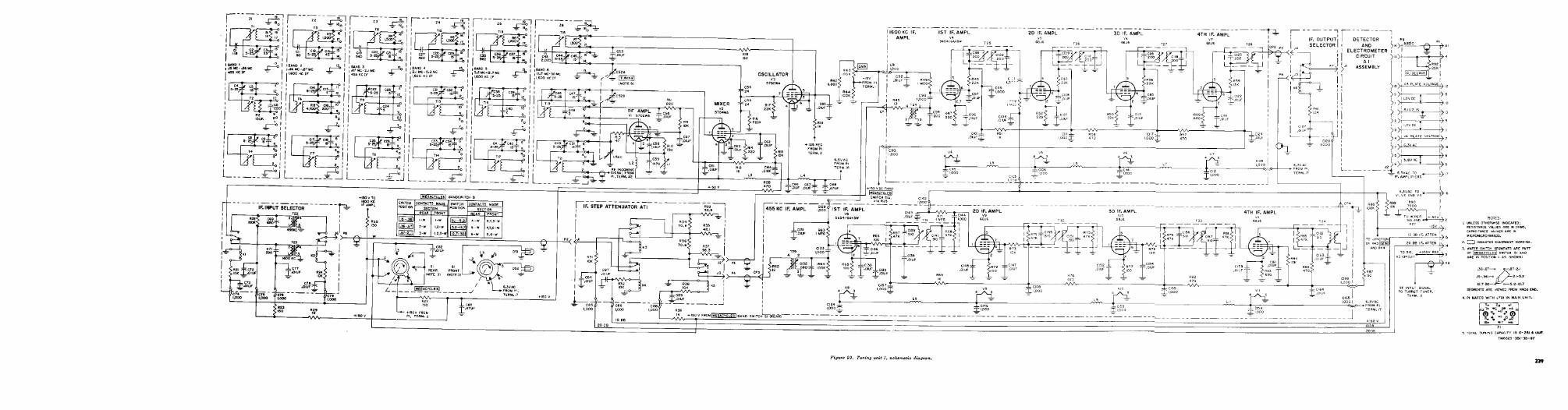
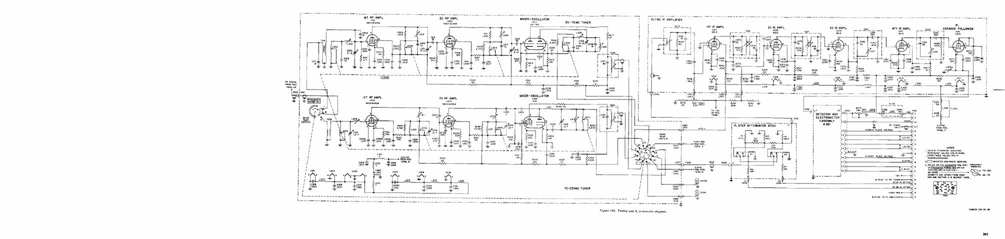
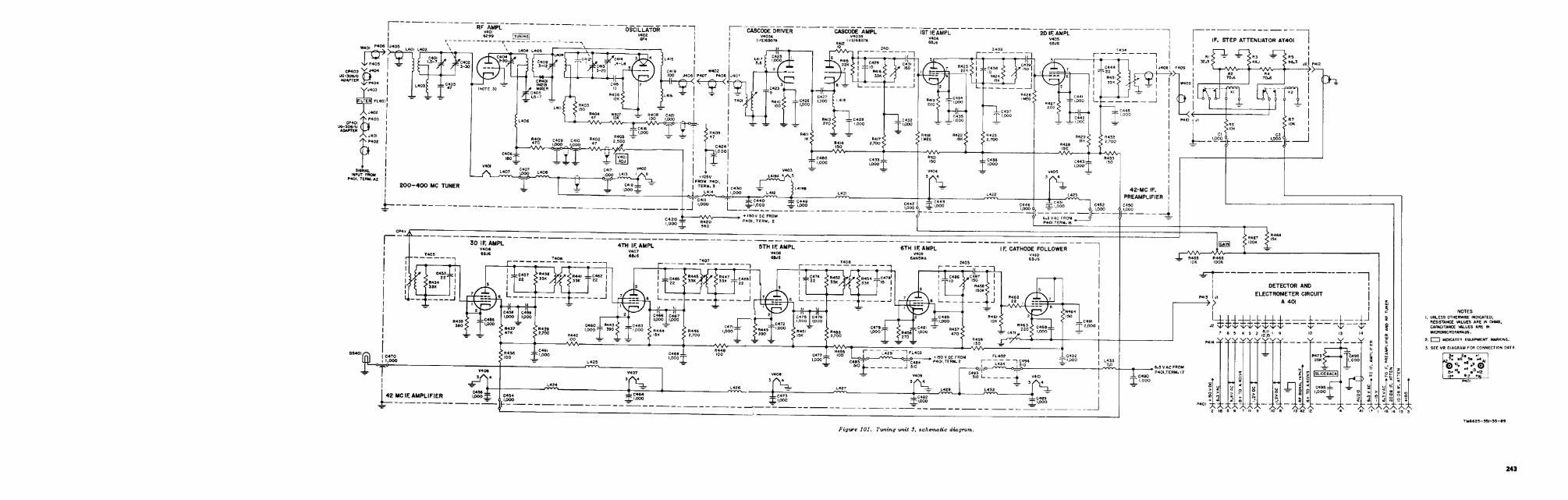
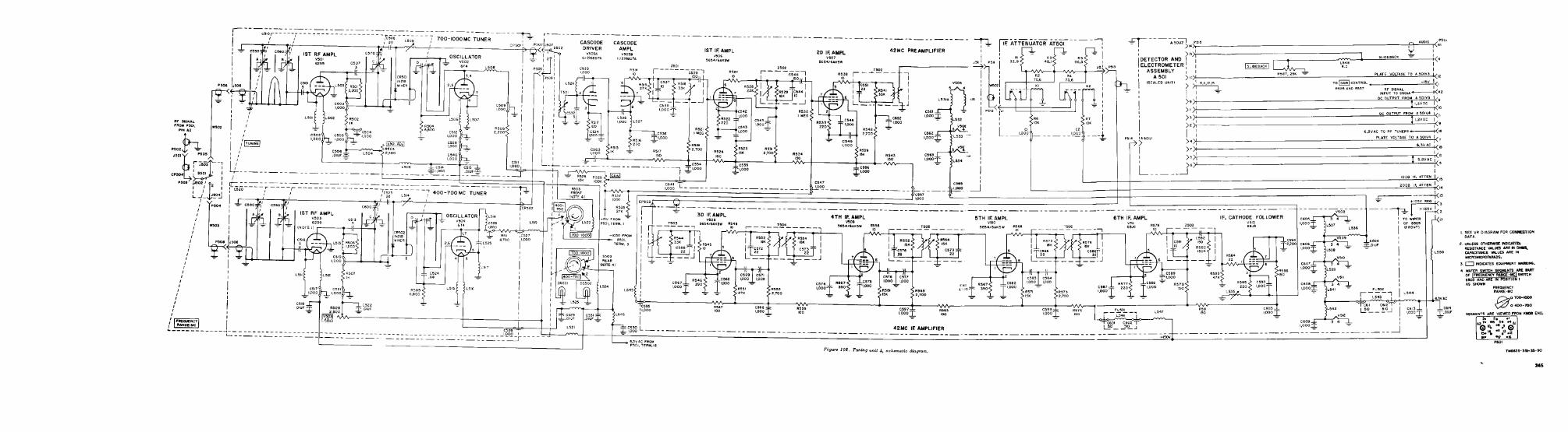
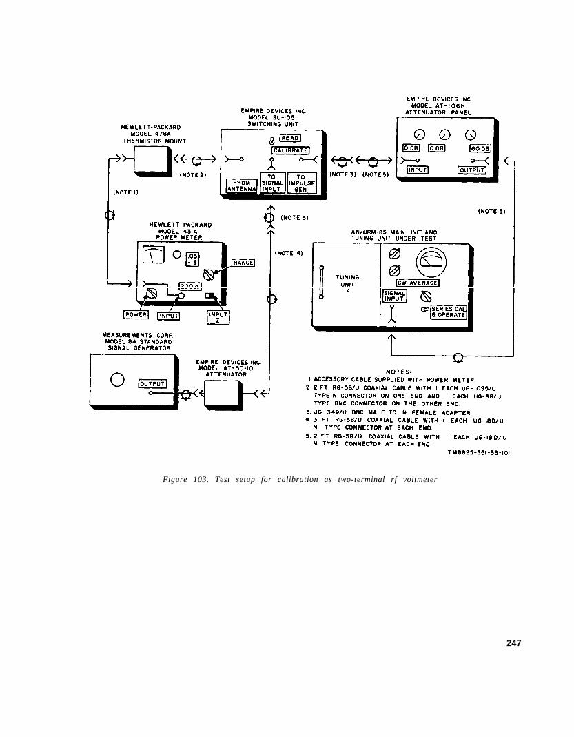
Figure 103. Test setup for calibration as two-terminal rf voltmeter
247
By Order of Secretary of the Army:
Official:J. C. LAMBERT,
Major General, United States Army,The Adjutant General.
Distribution:
Active Army::
DASA (6)USASA (2)CNGB (1)Tech Stf, DA (1) except
CSigO (14)Tech Stf Bd(1)USCON ARC (5)USAARTYBD (1)USAARMBD (2)USAIB (1)USARADBD (2)USAAVNBD (1)USAABELCTBD (1)USMTBD (1)ARADCOM (2)ARADCOM Rgn (2)OS Maj Cored (3)OS Base Cored (2)LOGCOMD (2)MDW (1)Armies (2)Corps (2)Instl (2)Ft Monmouth (63)USATC AD (2)USATC Armor (2)USATC Engr (2)USATC Inf (2)USATC FA (2)USAOMC (3)Svc Colleges (2)Br Svc Sch (2)GENDEP (2) except
Atlanta GENDEP (none)Sig Sec, GENDEP (5)Sig Dep (12)
G. H. DECKER,General, United States Army,
Chief of Staff.
WRAMC (1)USA Trans Tml Cored (1)Army Tml (1)POE (1)OSA (1)USAEPG (2)AFIP (1)AMS (1)Army Pictorial Cen (2)EMC (1)Yuma Test Sta (2)USACA (3)USASSA (20)USASSAMRO (1)USASEA (1)USARCARIB Sig Agcy (1)USA Sig Msl Spt Agcy (13)Sig Fld Maint Shops (3)USA Corps (3)Def Log Svc Cen (1)JBUSMC (2)1st GM Bde (2)AAF (CONUS) (2)Units org under fol TOE (2 c y each UNOINDC):
11-711-1611-5711-9811-11711-15511-15711-500 (AA-AE) (4)11-55711-58711-59211-597
NC: State AG (3); Units – Same as active Army except allowance is one copy to each unit.USAR: None.For explanation of abbreviations used, see AR 320-50.
U.S. GOVERNMENT PRINTING OFFICE : 1987 O–181-421 (60963)

TM 11-6625-351-35
RADIO INTERFERENCE MEASURING SET
AN/URM-85 — 1962
PIN : 017149-000


