Embed Size (px)
Citation preview
SRI VIDYA COLLEGE OF ENGINEERING AND TECHNOLOGY, VIRUDHUNAGAR COURSE MATERIAL (QB)
EC6504-MP&MC, UNIT 5 Page 1
Year/sem: 02/04 Academic Year: 2014-2015 (even)
UNIT V
THE 8086 SYSTEM BUS STRUCTURE
PART A
1. What are Timer Registers?
Timer registers are two 16-bit registers and can be accessed as their lower and upper bytes. TLO
represents the lower byte of the timing register 0, while THO represents higher bytes of the timing
register 0. Similarly, TLI and THI represent lower and higher bytes of timing register 1. These registers
can be accessed using the four addresses allotted to them, which lie in the special function registers
address range, i.e., 801 H to FF.
2. What is the use of Timing and Control Unit?
Timing and control unit is used to derive all the necessary timing and control signals required for the
internal operation of the circuit. It also derives control signals that are required for controlling the external
system bus.
3. What is The Purpose of A Gate Bit In Timer?
The gate is a secondary execution control bit. If the gate bit is reset, the timer is enabled to run at any
time. If the bit is set, then only when appropriate-INTn bit is high, the timer will run.
4. When are Timer Overflow Bits Set and Reset?
The timer overflow bits are set when timer rolls over and reset either by the execution of an ret instruction
or by software, manually clearing the bits. The bits are located in the TCON register along with timer run
control (TRn) bits.
5. Explain the Mode (0 And1) Operation Of The Timer.
The operations are as follows:
• Timer mode 0 and 1 operations are similar for the 13 bit (mode) or 16 bit (mode 1) counter. When the
timer reaches the limits of the count, the overflow flag is set and the counter is reset back to zero.
• The modes 0 and 1 can be used to time external events.
• They can be used as specific time delays by loading them with an initial value before allowing them to
execute and overflow.
6. What Is The Different Modes In Which Timer 2 Can Operate?
The two different modes in which Timer 2 operates are.
i. Capture mode
Timer 2 operates as free running clocks, which saves the timers value on each high to low transition. It
can be used for recording bit lengths when receiving Manchester-encoded data.
ii. Auto-reload mode:
When the timer overflows, value is written into TH2/TL2 registers from RCA P2H/RCA P21 registers.
This feature is used to implement a system watch dog timer.
7. What Is The Use Of A Watch Dog Timer?
SRI VIDYA COLLEGE OF ENGINEERING AND TECHNOLOGY, VIRUDHUNAGAR COURSE MATERIAL (QB)
EC6504-MP&MC, UNIT 5 Page 2
A watching timer is used to protect an application in case the controlling microcontroller begins to run
amok and execute randomly rather than the preprogrammed instructions written for the application.
8. Define Interrupt.
Interrupt is defined as request that can be refused. If not refused and when an interrupt request is
acknowledged, a special set of routine or events are followed to handle the interrupt.
9. What Are The Steps Followed To Service An Interrupt?
The steps followed are:
I. Save the context register information.
II. Reset the hardware requesting the interrupt.
III. Reset the interrupt controller.
IV. Process the interrupt.
V. Restore the context information.
VI. Return to the previously executing code.
10. How Can 8051 Be Interrupted?
There are five different ways to interrupt 8051. Two of these are from external electrical signals. The
other three are caused by internal 8051 I/O hardware operations.
11. What Are The Two Different Electrical Signals That Cause An Interrupt?
The two different electrical signals that cause an interrupt are:
I. Logic – 0 to Logic – 1 change known as transition activated interrupt.
II. Logic 0, Level activated interrupt.
12. Give The Format Of The Interrupt Enable Register.
The format of the interrupt enable register is,
EA - - ES ET1 EX1 ET0 EX0
The register is used to enable or disable all 8051 interrupts and to selectively enable or disable each of the
five different interrupts.
EA: Disables all interrupts
Es: Enables or disable the serial port interrupt.
ET1: Enable or disable the timer 1 overflow interrupt.
EX1: Enable or disable external interrupt 1.
ET0: Enable or disable the timer 0 overflow interrupt.
EX0: Enable or disable external interrupt 0.
13. What Is Meant By Nesting Of Interrupts?
Nesting of interrupts means that interrupts are re-enabled inside an interrupt handler. If another interrupt
request codes in, while the first interrupt handler is executing, processor execution will acknowledge the
new interrupt and jump to its vector.
14. How Is the 8051 Serial Port Different From other Micro Controllers?
The 8051 serial port is a very complex peripheral and able to send data synchronously and
asynchronously in a variety of different transmission modes.
15. Explain Synchronous Data Transmission.
• In synchronous mode (mode 0), the instruction clock is used.
SRI VIDYA COLLEGE OF ENGINEERING AND TECHNOLOGY, VIRUDHUNAGAR COURSE MATERIAL (QB)
EC6504-MP&MC, UNIT 5 Page 3
• Data transfer is initiated by writing to the serial data port address.
• Txd pin is used for clock output, while Rxd pin is for data transfer.
• When a character is received, the status of the data transfer is monitored by polling the RI-n bit in serial
control register (SCON).
16. Give An Application For Synchronous Serial Communiction.
An application for synchronous serial communication is RS – 232.
17. When Is An External Memory Access Generated In 8051?
In 8051, during execution the data is fetched continuous. Most of the data is executed out of the 8051‟s
built-in control store. When an address is outside the internal control store, an external memory access is
generated.
18. Write A Program To Save The Accumulator In R7 Of Bank 2.
CLR PSW – 3
SETB PSW – 4
MOV R7, A.
19. What Are Single Bit Instructions? Give Example.
Instructions that are used for single bit operation are called single bit instructions.
Examples: SETB bit
CLR bit
CPL bit
20. Write A Program To Save The Status Of Bits P1.2 And P1.3 On Ram Bit Locations 6 And
7 Respectively.
MOV C, P1.2 ; save status of P1.2 on CY
MOV O6, C ; save carry in RAM bit location 06
MOV C, p1.3 ; save status of p1.3 on CY
MOV 07, C ; save carry in RAM bit location 07.
21. Write A Program To See If Bits 0 And 5 Of Register B R1. If They Are Not, Make Them So
And Save It In R0.
JNB OFOH, NEXT – 1 ; JUMP if B.0 is low
SET BOFOH ; Make bit B.0 high
NEXT – 1:JNB OF5H, NEXT – 2 ; JUMP if B.5 is low
SETB OF5H ; Make B.5 high
NEXT – 2: MOV R0, B ; Save register B.
22. Give The Priority Level of The Interrupt Sources.
Interrupt source Priority within a level
IE0 (External INT0 )
TF0(Timer 0)
IE 1 (External INT 1)
TF 1 (Timer 1)
RI = TI (Serial port) Highest
.
.
SRI VIDYA COLLEGE OF ENGINEERING AND TECHNOLOGY, VIRUDHUNAGAR COURSE MATERIAL (QB)
EC6504-MP&MC, UNIT 5 Page 4
.
Lowest
23. Write any four LCD commands
1. Clear display screen, CLR
2. Decrement Cursor
3. Display OFF
4. Shift display left
24. What do you mean by key debouncing
When a switch or key is pressed it does not fully close the first time you press it because the metal
contacts bounce off each other!
Feeding the signal into a logic gate or a microcontroller sends multiple key press signals which is not
what you want so you have to ignore the bouncing signal - this is known as debouncing the switch or key.
PART B
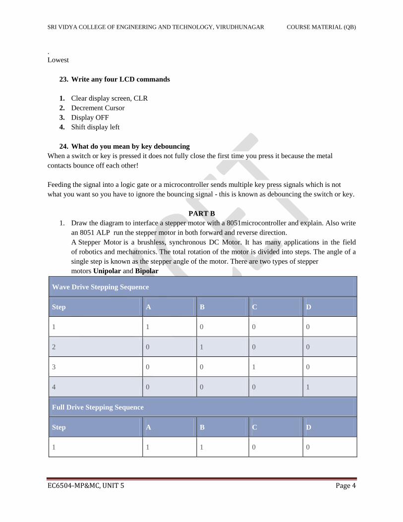
1. Draw the diagram to interface a stepper motor with a 8051microcontroller and explain. Also write
an 8051 ALP run the stepper motor in both forward and reverse direction.
A Stepper Motor is a brushless, synchronous DC Motor. It has many applications in the field
of robotics and mechatronics. The total rotation of the motor is divided into steps. The angle of a
single step is known as the stepper angle of the motor. There are two types of stepper
motors Unipolar and Bipolar
Wave Drive Stepping Sequence
Step A B C D
1 1 0 0 0
2 0 1 0 0
3 0 0 1 0
4 0 0 0 1
Full Drive Stepping Sequence
Step A B C D
1 1 1 0 0
SRI VIDYA COLLEGE OF ENGINEERING AND TECHNOLOGY, VIRUDHUNAGAR COURSE MATERIAL (QB)
EC6504-MP&MC, UNIT 5 Page 5
2 0 1 1 0
3 0 0 1 1
4 1 0 0 1
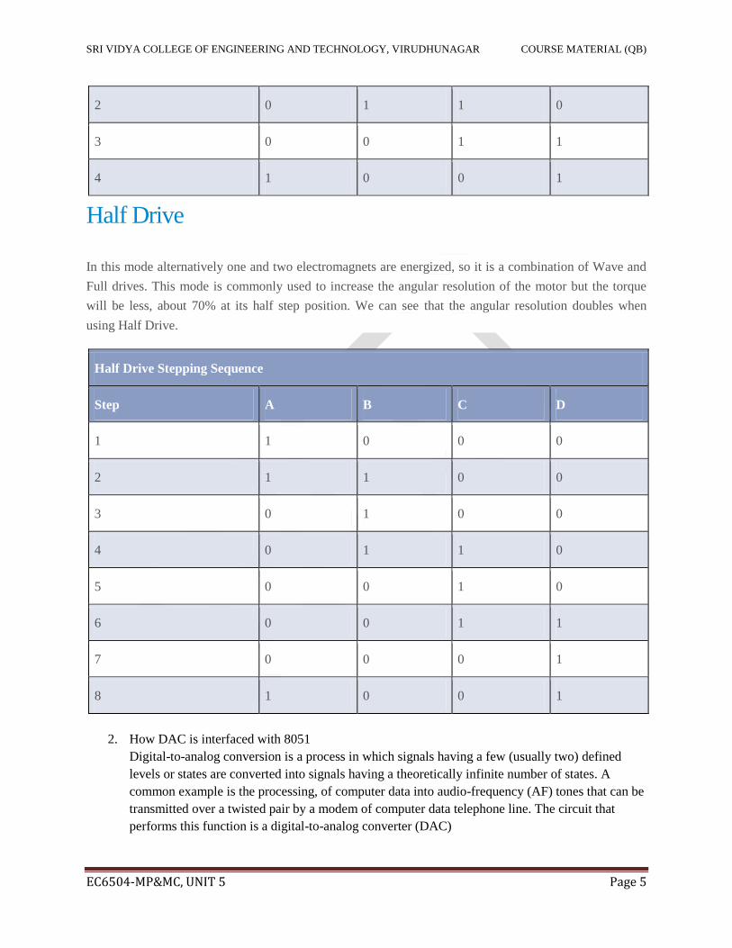
Half Drive
In this mode alternatively one and two electromagnets are energized, so it is a combination of Wave and
Full drives. This mode is commonly used to increase the angular resolution of the motor but the torque
will be less, about 70% at its half step position. We can see that the angular resolution doubles when
using Half Drive.
Half Drive Stepping Sequence
Step A B C D
1 1 0 0 0
2 1 1 0 0
3 0 1 0 0
4 0 1 1 0
5 0 0 1 0
6 0 0 1 1
7 0 0 0 1
8 1 0 0 1
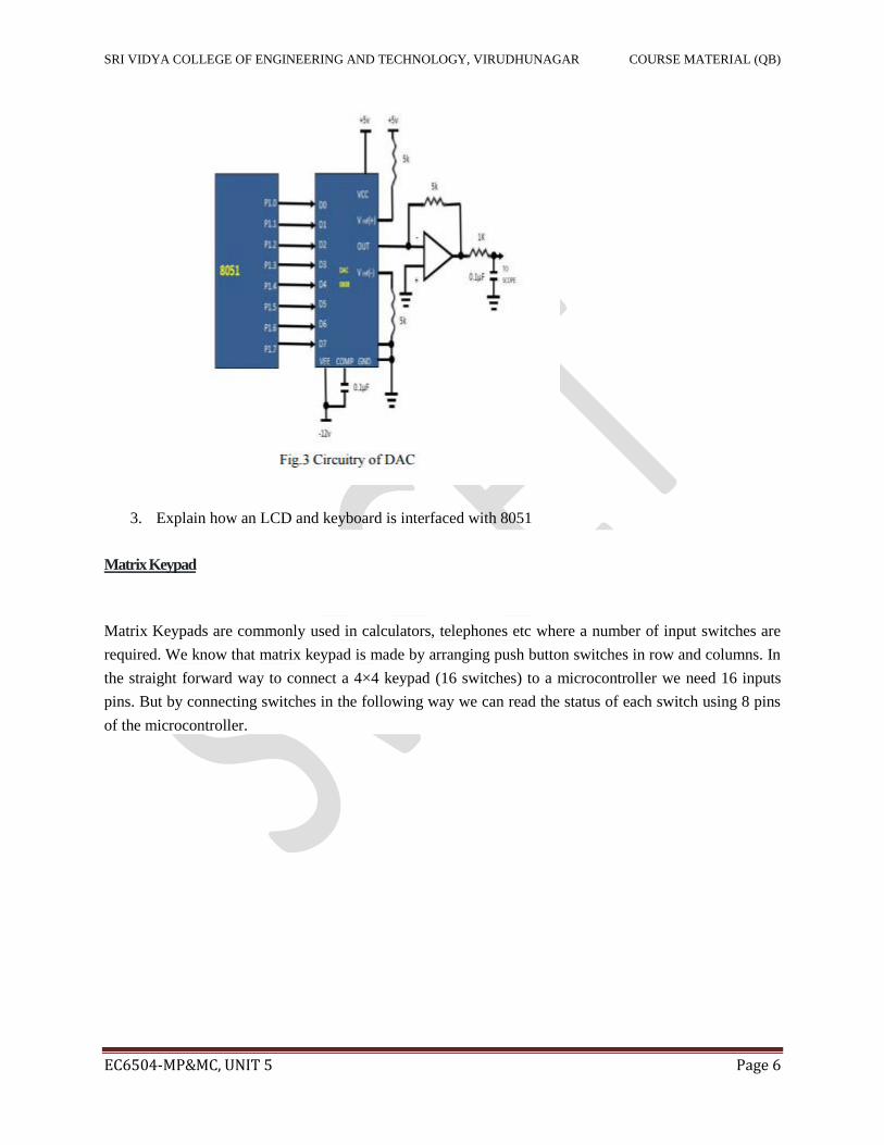
2. How DAC is interfaced with 8051
Digital-to-analog conversion is a process in which signals having a few (usually two) defined
levels or states are converted into signals having a theoretically infinite number of states. A
common example is the processing, of computer data into audio-frequency (AF) tones that can be
transmitted over a twisted pair by a modem of computer data telephone line. The circuit that
performs this function is a digital-to-analog converter (DAC)
SRI VIDYA COLLEGE OF ENGINEERING AND TECHNOLOGY, VIRUDHUNAGAR COURSE MATERIAL (QB)
EC6504-MP&MC, UNIT 5 Page 6
3. Explain how an LCD and keyboard is interfaced with 8051
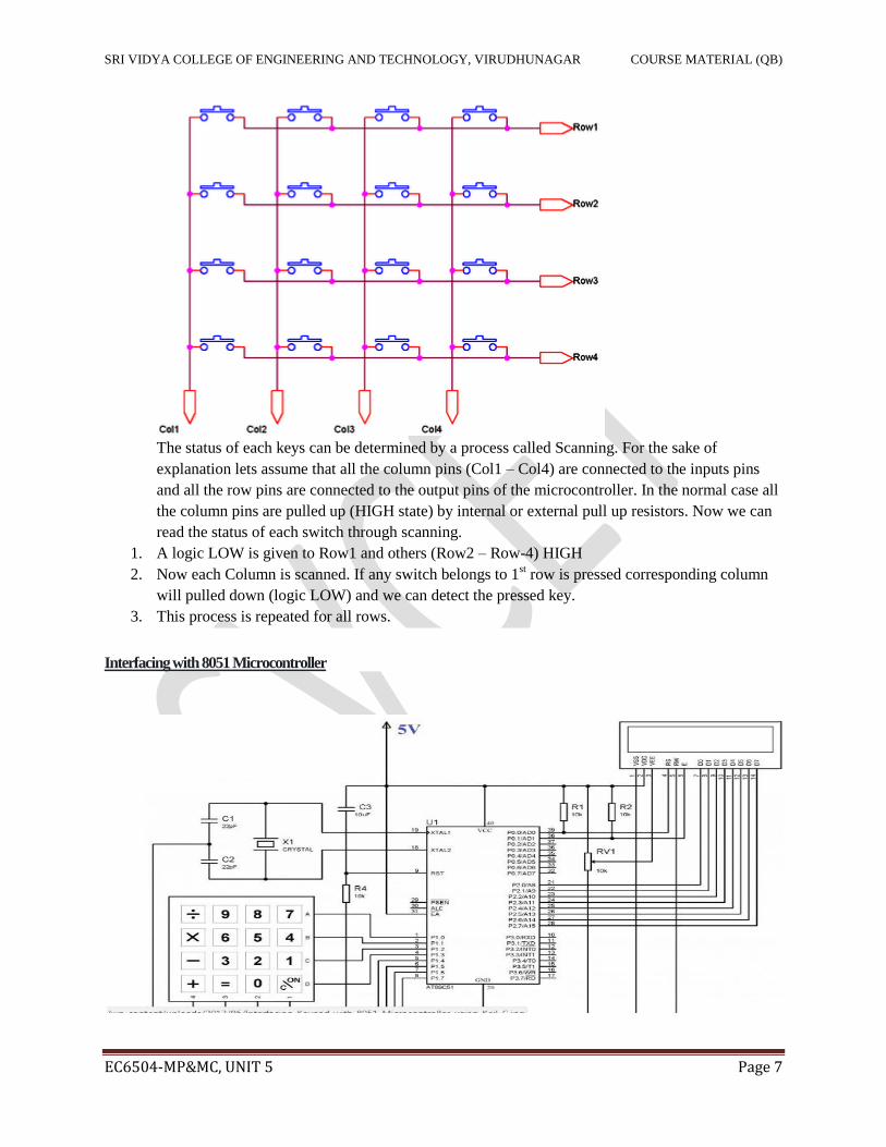
Matrix Keypad
Matrix Keypads are commonly used in calculators, telephones etc where a number of input switches are
required. We know that matrix keypad is made by arranging push button switches in row and columns. In
the straight forward way to connect a 4×4 keypad (16 switches) to a microcontroller we need 16 inputs
pins. But by connecting switches in the following way we can read the status of each switch using 8 pins
of the microcontroller.
SRI VIDYA COLLEGE OF ENGINEERING AND TECHNOLOGY, VIRUDHUNAGAR COURSE MATERIAL (QB)
EC6504-MP&MC, UNIT 5 Page 7
The status of each keys can be determined by a process called Scanning. For the sake of
explanation lets assume that all the column pins (Col1 – Col4) are connected to the inputs pins
and all the row pins are connected to the output pins of the microcontroller. In the normal case all
the column pins are pulled up (HIGH state) by internal or external pull up resistors. Now we can
read the status of each switch through scanning.
1. A logic LOW is given to Row1 and others (Row2 – Row-4) HIGH
2. Now each Column is scanned. If any switch belongs to 1st row is pressed corresponding column
will pulled down (logic LOW) and we can detect the pressed key.
3. This process is repeated for all rows.
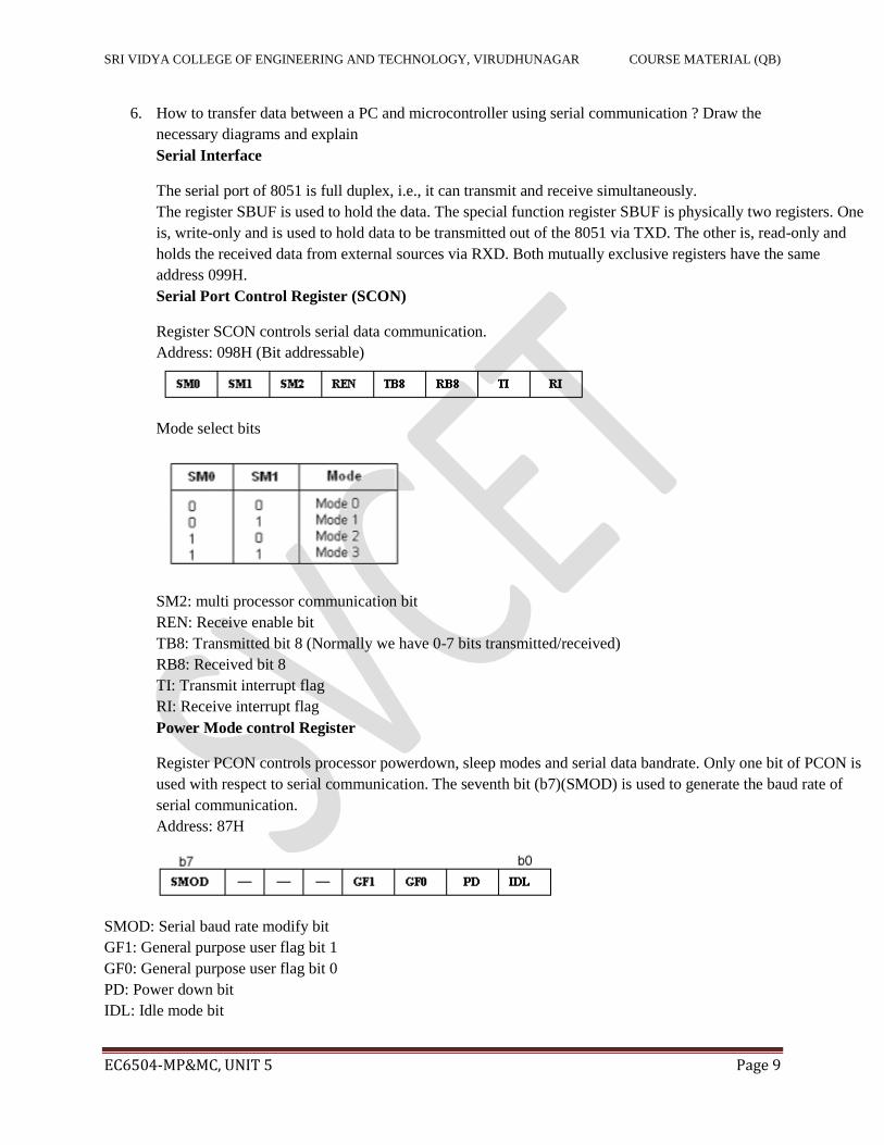
Interfacing with 8051 Microcontroller

SRI VIDYA COLLEGE OF ENGINEERING AND TECHNOLOGY, VIRUDHUNAGAR COURSE MATERIAL (QB)
EC6504-MP&MC, UNIT 5 Page 8
4. Explain the interfacing of 4x4 matrix keyboard to the 8051 microcontroller with neat diagram
Matrix Keypad Interface Logic
Initially all switches are assumed to be released. So there is no connection between the rows and
columns. When any one of the switches are pressed, the corresponding rows and columns are connected
(short circuited). This will drive that column pin (initially high) low. Using this logic, the button press can
be detected. The colors red and black are for logic high and low respectively. Here are the steps involved
in determining the key that was pressed.
5. Write shortly on the various operating modes for serial port of 8051 microcontroller
1. Setting the serial port mode
2. Writing to the serial port
3. Setting the serial Baud rate
4. Reading from the serial port
SRI VIDYA COLLEGE OF ENGINEERING AND TECHNOLOGY, VIRUDHUNAGAR COURSE MATERIAL (QB)
EC6504-MP&MC, UNIT 5 Page 9
6. How to transfer data between a PC and microcontroller using serial communication ? Draw the
necessary diagrams and explain
Serial Interface
The serial port of 8051 is full duplex, i.e., it can transmit and receive simultaneously.
The register SBUF is used to hold the data. The special function register SBUF is physically two registers. One
is, write-only and is used to hold data to be transmitted out of the 8051 via TXD. The other is, read-only and
holds the received data from external sources via RXD. Both mutually exclusive registers have the same
address 099H.
Serial Port Control Register (SCON)
Register SCON controls serial data communication.
Address: 098H (Bit addressable)
Mode select bits
SM2: multi processor communication bit
REN: Receive enable bit
TB8: Transmitted bit 8 (Normally we have 0-7 bits transmitted/received)
RB8: Received bit 8
TI: Transmit interrupt flag
RI: Receive interrupt flag
Power Mode control Register
Register PCON controls processor powerdown, sleep modes and serial data bandrate. Only one bit of PCON is
used with respect to serial communication. The seventh bit (b7)(SMOD) is used to generate the baud rate of
serial communication.
Address: 87H
SMOD: Serial baud rate modify bit
GF1: General purpose user flag bit 1
GF0: General purpose user flag bit 0
PD: Power down bit
IDL: Idle mode bit
SRI VIDYA COLLEGE OF ENGINEERING AND TECHNOLOGY, VIRUDHUNAGAR COURSE MATERIAL (QB)
EC6504-MP&MC, UNIT 5 Page 10
Data Transmission
Transmission of serial data begins at any time when data is written to SBUF. Pin P3.1 (Alternate function bit
TXD) is used to transmit data to the serial data network. TI is set to 1 when data has been transmitted. This
signifies that SBUF is empty so that another byte can be sent.
Data Reception
Reception of serial data begins if the receive enable bit is set to 1 for all modes. Pin P3.0 (Alternate function
bit RXD) is used to receive data from the serial data network. Receive interrupt flag, RI, is set after the datahas
been received in all modes. The data gets stored in SBUF register from where it can be read.
Serial Data Transmission Modes:
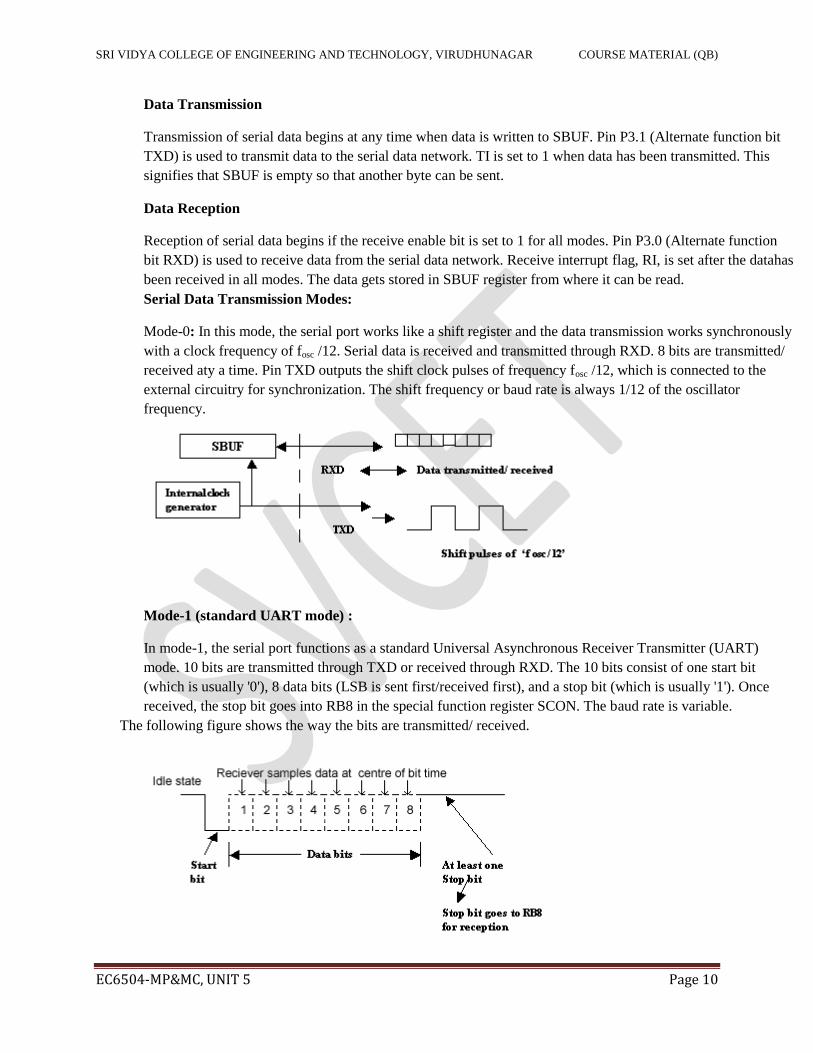
Mode-0: In this mode, the serial port works like a shift register and the data transmission works synchronously
with a clock frequency of fosc /12. Serial data is received and transmitted through RXD. 8 bits are transmitted/
received aty a time. Pin TXD outputs the shift clock pulses of frequency fosc /12, which is connected to the
external circuitry for synchronization. The shift frequency or baud rate is always 1/12 of the oscillator
frequency.
Mode-1 (standard UART mode) :
In mode-1, the serial port functions as a standard Universal Asynchronous Receiver Transmitter (UART)
mode. 10 bits are transmitted through TXD or received through RXD. The 10 bits consist of one start bit
(which is usually '0'), 8 data bits (LSB is sent first/received first), and a stop bit (which is usually '1'). Once
received, the stop bit goes into RB8 in the special function register SCON. The baud rate is variable.
The following figure shows the way the bits are transmitted/ received.
SRI VIDYA COLLEGE OF ENGINEERING AND TECHNOLOGY, VIRUDHUNAGAR COURSE MATERIAL (QB)
EC6504-MP&MC, UNIT 5 Page 11
Bit time= 1/fbaud
In receiving mode, data bits are shifted into the receiver at the programmed baud rate. The data word (8-bits)
will be loaded to SBUF if the following conditions are true.
RI must be zero. (i.e., the previously received byte has been cleared from SBUF)
Mode bit SM2 = 0 or stop bit = 1.
After the data is received and the data byte has been loaded into SBUF, RI becomes one.
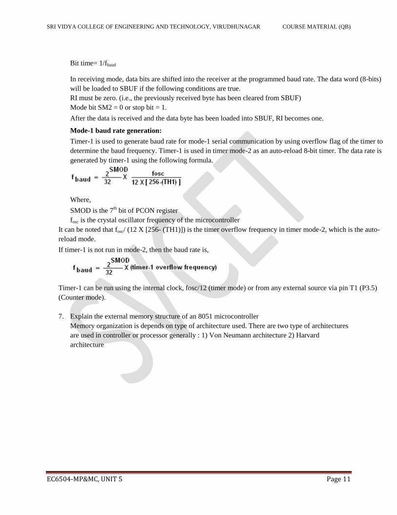
Mode-1 baud rate generation:
Timer-1 is used to generate baud rate for mode-1 serial communication by using overflow flag of the timer to
determine the baud frequency. Timer-1 is used in timer mode-2 as an auto-reload 8-bit timer. The data rate is
generated by timer-1 using the following formula.
Where,
SMOD is the 7th bit of PCON register
fosc is the crystal oscillator frequency of the microcontroller
It can be noted that fosc/ (12 X [256- (TH1)]) is the timer overflow frequency in timer mode-2, which is the auto-
reload mode.
If timer-1 is not run in mode-2, then the baud rate is,
Timer-1 can be run using the internal clock, fosc/12 (timer mode) or from any external source via pin T1 (P3.5)
(Counter mode).
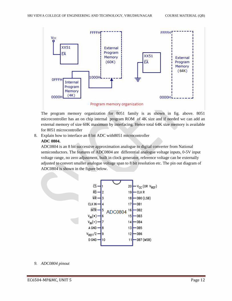
7. Explain the external memory structure of an 8051 microcontroller
Memory organization is depends on type of architecture used. There are two type of architectures
are used in controller or processor generally : 1) Von Neumann architecture 2) Harvard
architecture
SRI VIDYA COLLEGE OF ENGINEERING AND TECHNOLOGY, VIRUDHUNAGAR COURSE MATERIAL (QB)
EC6504-MP&MC, UNIT 5 Page 12
The program memory organization for 8051 family is as shown in fig. above. 8051
microcontroller has an on chip internal program ROM of 4K size and if needed we can add an
external memory of size 60K maximum by interfacing. Hence total 64K size memory is available
for 8051 microcontroller
8. Explain how to interface an 8 bit ADC with8051 microcontroller
ADC 0804.
ADC0804 is an 8 bit successive approximation analogue to digital converter from National
semiconductors. The features of ADC0804 are differential analogue voltage inputs, 0-5V input
voltage range, no zero adjustment, built in clock generator, reference voltage can be externally
adjusted to convert smaller analogue voltage span to 8 bit resolution etc. The pin out diagram of
ADC0804 is shown in the figure below.
9. ADC0804 pinout
SRI VIDYA COLLEGE OF ENGINEERING AND TECHNOLOGY, VIRUDHUNAGAR COURSE MATERIAL (QB)
EC6504-MP&MC, UNIT 5 Page 13
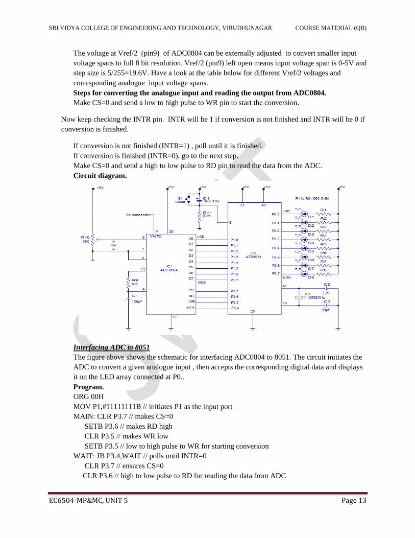
The voltage at Vref/2 (pin9) of ADC0804 can be externally adjusted to convert smaller input
voltage spans to full 8 bit resolution. Vref/2 (pin9) left open means input voltage span is 0-5V and
step size is 5/255=19.6V. Have a look at the table below for different Vref/2 voltages and
corresponding analogue input voltage spans.
Steps for converting the analogue input and reading the output from ADC0804.
Make CS=0 and send a low to high pulse to WR pin to start the conversion.
Now keep checking the INTR pin. INTR will be 1 if conversion is not finished and INTR will be 0 if
conversion is finished.
If conversion is not finished (INTR=1) , poll until it is finished.
If conversion is finished (INTR=0), go to the next step.
Make CS=0 and send a high to low pulse to RD pin to read the data from the ADC.
Circuit diagram.
Interfacing ADC to 8051
The figure above shows the schematic for interfacing ADC0804 to 8051. The circuit initiates the
ADC to convert a given analogue input , then accepts the corresponding digital data and displays
it on the LED array connected at P0..
Program.
ORG 00H
MOV P1,#11111111B // initiates P1 as the input port
MAIN: CLR P3.7 // makes CS=0
SETB P3.6 // makes RD high
CLR P3.5 // makes WR low
SETB P3.5 // low to high pulse to WR for starting conversion
WAIT: JB P3.4,WAIT // polls until INTR=0
CLR P3.7 // ensures CS=0
CLR P3.6 // high to low pulse to RD for reading the data from ADC
SRI VIDYA COLLEGE OF ENGINEERING AND TECHNOLOGY, VIRUDHUNAGAR COURSE MATERIAL (QB)
EC6504-MP&MC, UNIT 5 Page 14
MOV A,P1 // moves the digital data to accumulator
CPL A // complements the digital data (*see the notes)
MOV P0,A // outputs the data to P0 for the LEDs
SJMP MAIN // jumps back to the MAIN program
END
Explain interrupt programming in detail
The Microcontroller can serve several devices. The Interrupt is the method to indicate the
microcontroller by sending it an interrupt signal. After receiving an interrupt, the microcontroller
interrupts what ever it is doing and serves the device. The program associated with the interrupt is
called the interrupt service and routine (ISR).
Interrupt Vector Table
NT0 0003H
TIMER0 000BH
INT1 0013H
TIMER1 001BH
SERIAL COMMUNICATION INTERRUPT 0023H
Step in executing an Interrupt:
1) It finish the instruction it is executing and saves the address of the next instruction (PC) on the stack.
2) It also saves the current status of all the interrupt internally.
3) It Jumps to a fixed location in memory called the interrupt vector table that holds the address of the
interrupt service routine.
4) The microcontroller gets the address of the ISR from the interrupt vector and jumps to it. It starts to
execute the interrupt service subroutine until it reaches the last instruction of the subroutine.
5) Upon executing the RETI instruction ,the microcontroller returns to the Place where it was interrupt.
Interrupt Enable Register (EA)
D7 D6 D5 D4 D3 D2 D1 D0
EA - - ES ET1 EX1 ET0 EX0
SRI VIDYA COLLEGE OF ENGINEERING AND TECHNOLOGY, VIRUDHUNAGAR COURSE MATERIAL (QB)
EC6504-MP&MC, UNIT 5 Page 15
EA IE.7 Disable all interrupts .
If EA= 0 no interrupt is acknowledged If
EA=1 , each interrupt source is individually Enable or disable
By setting or clearing the enable or disable
ES IE.4 Enable or disable the serial port interrupt
ET1 IE.3 Enable or disable Timer 1 overflow interrupt
EX1 IE.2 Enable or disable external interrupt 1
ET0 IE.1 Enable or disable Timer 0 overflow interrupt.
EX0 IE.0 Enable or disable external interrupt 0.
Enabling and disabling Interrupts
Upon reset all interrupts are disable, meaning that known will be responded to by the microcontroller if
they are activated. The Interrupt must be enabled by software in order for microcontroller to respond to
them there is a register called IE that is responsible for enabling and disabling the interrupts.
Steps in Enable an Interrupt
To enable an interrupt an interrupt we take following steps.
1.Bit D7 of the IE Register must to set to high to allow the rest of register to take effect.
2.If EA=1, interrupts are enable and will to responded to if this corresponding bits in IE are High. If
EA=1, No Interrupt will be responeded.
Programming External Hardware Interrupts
The 8051 has two external hardware interrupts PIN 12 (P3.2) and Pin 13 (P3.3) of the 8051, designated as
INT0 and INT1 are used as external hardware interrupts. Upon activation of these pins, the 8051 gets
interrupts in what ever it is doing and jumps to the vector table to perform the interrupt service routine
Type of Interrupt
1)Level-Triggered Interrupt
2)Edge -Triggered Interrupt
Level-Triggered Interrupt
In this mode, INT0 and INT1 are normally high and if the low level signal is applied to them ,It triggers
SRI VIDYA COLLEGE OF ENGINEERING AND TECHNOLOGY, VIRUDHUNAGAR COURSE MATERIAL (QB)
EC6504-MP&MC, UNIT 5 Page 16
the Interrupt. Then the microcontroller stops and jumps to the interrupt vector table to service that
interrupt .This is all the Level Triggered or Level -Activated interrupt and is the default mode/reset of
8051.
Edge -Triggered Interrupt
Upon reset 8051 makes INT0 and INT1 low l Level-Triggered Interrupt. To make them Edge -Triggered
Interrupt, we must program the bits of the TCON Register. The TCON register holds among other bits
and IT0 and IT1 flags bit the determine level- or edge triggered mode. Of the hardware interrupt IT0 and
IT1 and bits D0 and D2 of the TCON Register Respectively. In this Section, we have discuss only INT0
and INT1 External Hardware Interrupts.


