Embed Size (px)
Citation preview

MAHARASHTRA STATE BOARD OF TECHNICAL EDUCATION (Autonomous)
(ISO/IEC - 27001 - 2013 Certified)
__________________________________________________________________________________________________
Page 1/16
WINTER – 19EXAMINATION Subject Name:Applied Electronics Model AnswerSubject Code:
Important Instructions to examiners:
1) The answers should be examined by key words and not as word-to-word as given in themodel answer scheme.
2) The model answer and the answer written by candidate may vary but the examiner may tryto assess the understanding level of the candidate.
3) The language errors such as grammatical, spelling errors should not be given moreImportance (Not applicable for subject English and Communication Skills.
4) While assessing figures, examiner may give credit for principal components indicated in thefigure. The figures drawn by candidate and model answer may vary. The examiner may give credit for anyequivalent figure drawn.
5) Credits may be given step wise for numerical problems. In some cases, the assumed constantvalues may vary and there may be some difference in the candidate’s answers and model answer.
6) In case of some questions credit may be given by judgement on part of examiner of relevant answer based on candidate’s understanding.
7) For programming language papers, credit may be given to any other program based on equivalent concept.
Q. No.
Sub Q. N.
Answer Marking Scheme
Q.1 Attempt any FIVE of the following: 10-Total
Marks
a) List the types of coupling used in BJT amplifier. 2M
Ans: Types of coupling used in BJT amplifier:
i. Resistance capacitance (RC)coupling
ii. Impedance coupling
iii. Transformer coupling
iv. Direct coupling
Each ½ M
b) Compare small signal amplifier with power amplifier(any four) 2M
Ans: Sr.No Parameters Small signal
Amplifiers
Power Amplifiers
1
Amplification
quantity
It increases voltage
into high resistance
load. Hence small
signal amplifiers are
also called as
voltage amplifiers.
It increases power
into low resistance
load. Hence these
amplifiers are also
called as large
signal amplifiers.
2 Current
Gain(β)
High(typically 100) Low(5 to 20)
3 Input
Resistance(Ri)
Quite low Very large
4 Output High low
Any four
points:
each ½ M
22329

MAHARASHTRA STATE BOARD OF TECHNICAL EDUCATION (Autonomous)
(ISO/IEC - 27001 - 2013 Certified)
__________________________________________________________________________________________________
Page 2/16
Impedance(Ro)
5 Physical size Small Large in size
6 Coupling R-C coupling Transformer
coupling
7 Power output low High
c) State four advantages of negative feedback used in feedback amplifier. 2M
Ans: Advantages of negative feedback: (Any Four)
i. Distortion decreases
ii. Noise in output decreases
iii. Stability of gain of amplifier improves
iv. It is used as an amplifier.
v. Operating point is stabilized.
vi. Input resistance increases in certain configuration and output resistance decreases in
certain configurations.
vii. Bandwidth is increased
Each ½ M
d) State Barkhausen criteria of oscillation. 2M
Ans: Where, AV = gain of an amplifier without feedback also called open loop gain
β AV = product of feedback fraction and open loop gain. It is called loop gain.
The Barkhausen criterion for the generation of sustained oscillations. for positive feedback
are:
1. β A = 1
2. Total phase shift should be 360° or 0°
1M
1M
e) Differentiate positive feedback and negative feedback (four points) 2M
Ans: Sr.
No.
Parameter Positive feedback Negative feedback
1 Feedback signal In phase with the input
signal.
180 º out of phase
with the input signal.
2 Net input signal Increases Decreases
3 Gain Increases Decreases
4 Noise Increases Increases Decreases
5 Stability Poor Improved
6 Input impedance decreases increases
7 Output impedance increases decreases
8 Uses Oscillators, Schmitt
trigger
Amplifiers,
bootstrapping
Any Four
points
Each ½ M
MAHARASHTRA STATE BOARD OF TECHNICAL EDUCATION (Autonomous)
(ISO/IEC - 27001 - 2013 Certified)
__________________________________________________________________________________________________
Page 3/16
f) State the need of tuned amplifier in electronic circuits.(four points) 2M
Ans: (Note:Any two points can be given full marks)
Need of tuned amplifier:
i. Selects the desired radio frequency signal.
ii. Amplifies the selected high or radiosignal to a suitable voltage level.
iii. As a filter.
2M
g) List the uses of heat sink (four points) 2M
Ans: Uses of heat sink:
i. It is used to avoid thermal runaway in electronic circuits.
ii. Use to transfer heat generated by a mechanical or an electronic device to the
surroundings.
iii. Use to optimize the heat exchange between component and surrounding by
maximizing the contact surface between heat sink and air.
iv. Used to dissipate the amount of heat generated.
Each
point
½ M
Q.2 Attempt any THREE of the following: 12-Total
Marks
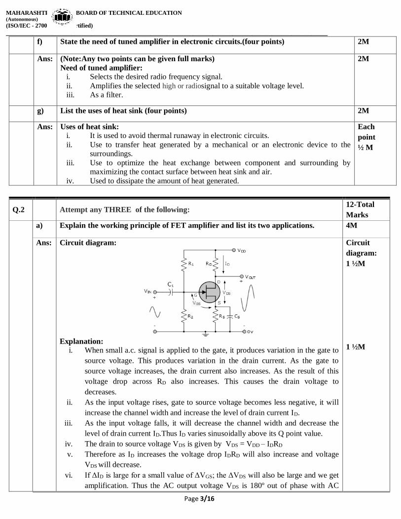
a) Explain the working principle of FET amplifier and list its two applications. 4M
Ans: Circuit diagram:
Explanation:
i. When small a.c. signal is applied to the gate, it produces variation in the gate to
source voltage. This produces variation in the drain current. As the gate to
source voltage increases, the drain current also increases. As the result of this
voltage drop across RD also increases. This causes the drain voltage to
decreases.
ii. As the input voltage rises, gate to source voltage becomes less negative, it will
increase the channel width and increase the level of drain current ID.
iii. As the input voltage falls, it will decrease the channel width and decrease the
level of drain current ID.Thus ID varies sinusoidally above its Q point value.
iv. The drain to source voltage VDS is given by VDS = VDD – IDRD
v. Therefore as ID increases the voltage drop IDRD will also increase and voltage
VDS will decrease.
vi. If ΔID is large for a small value of ΔVGS; the ΔVDS will also be large and we get
amplification. Thus the AC output voltage VDS is 180º out of phase with AC
Circuit
diagram:
1 ½M
1 ½M
MAHARASHTRA STATE BOARD OF TECHNICAL EDUCATION (Autonomous)
(ISO/IEC - 27001 - 2013 Certified)
__________________________________________________________________________________________________
Page 4/16
input voltage.
Applications: (Any 2)
i. Low noise amplifier
ii. Buffer amplifier
iii. Cascade amplifier
iv. Analog switch
v. Multiplexer
vi. Chopper
vii. Current limiter
1M
(1/2 M
each)
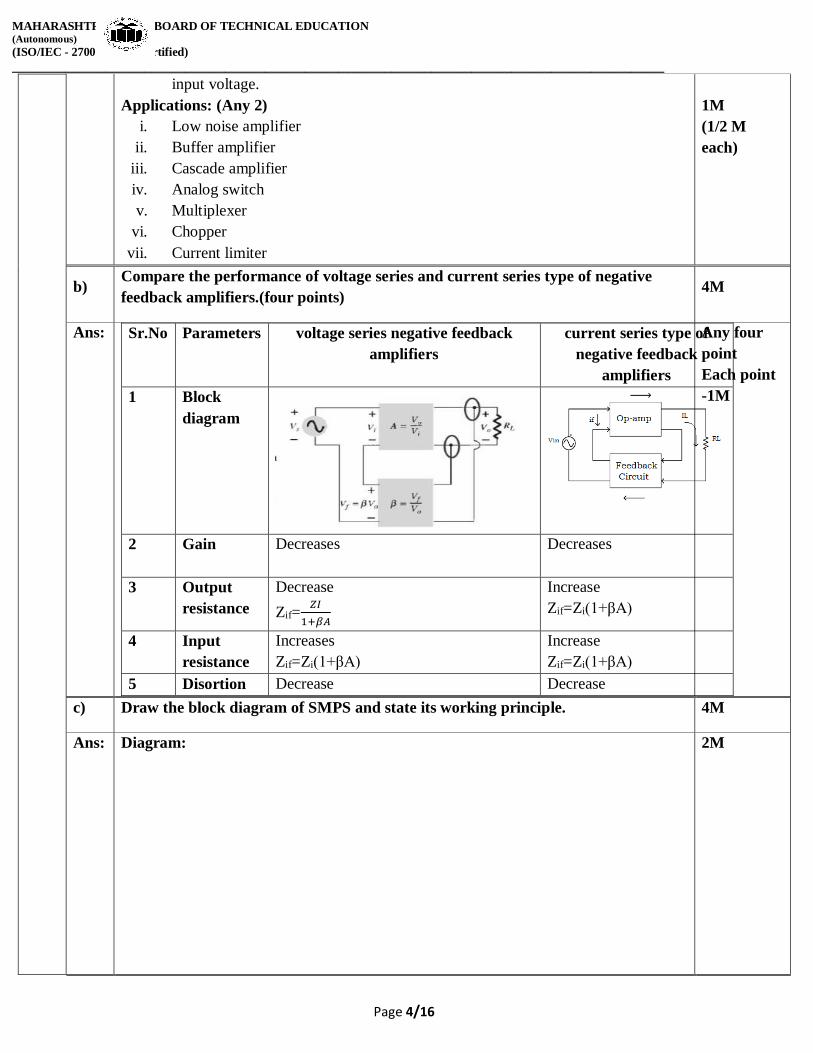
b) Compare the performance of voltage series and current series type of negative
feedback amplifiers.(four points) 4M
Ans: Sr.No Parameters voltage series negative feedback
amplifiers
current series type of
negative feedback
amplifiers
1 Block
diagram
2 Gain Decreases
Decreases
3 Output
resistance
Decrease
Zif=𝑍𝐼
1+𝛽𝐴
Increase
Zif=Zi(1+βA)
4 Input
resistance
Increases
Zif=Zi(1+βA)
Increase
Zif=Zi(1+βA)
5 Disortion Decrease Decrease
Any four
point
Each point
-1M
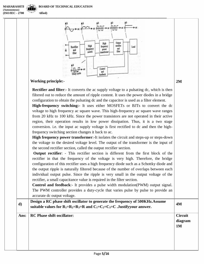
c) Draw the block diagram of SMPS and state its working principle. 4M
Ans: Diagram:
2M
MAHARASHTRA STATE BOARD OF TECHNICAL EDUCATION (Autonomous)
(ISO/IEC - 27001 - 2013 Certified)
__________________________________________________________________________________________________
Page 5/16
Working principle:-
Rectifier and filter:- It converts the ac supply voltage to a pulsating dc, which is then
filtered out to reduce the amount of ripple content. It uses the power diodes in a bridge
configuration to obtain the pulsating dc and the capacitor is used as a filter element.
High-frequency switching:- It uses either MOSFETs or BJTs to convert the dc
voltage to high frequency ac square wave. This high-frequency ac square wave ranges
from 20 kHz to 100 kHz. Since the power transistors are not operated in their active
region, their operation results in low power dissipation. Thus, it is a two stage
conversion. i.e. the input ac supply voltage is first rectified to dc and then the high-
frequency switching section changes it back to ac.
High frequency power transformer:-It isolates the circuit and steps-up or steps-down
the voltage to the desired voltage level. The output of the transformer is the input of
the second rectifier section, called the output rectifier section.
Output rectifier: - This rectifier section is different from the first block of the
rectifier in that the frequency of the voltage is very high. Therefore, the bridge
configuration of this rectifier uses a high frequency diode such as a Schottky diode and
the output ripple is naturally filtered because of the number of overlaps between each
individual output pulse. Since the ripple is very small in the output voltage of the
rectifier, a small capacitance value is required in the filter section.
Control and feedback:- It provides a pulse width modulation(PWM) output signal.
The PWM controller provides a duty-cycle that varies pulse by pulse to provide an
accurate dc output voltage.
2M
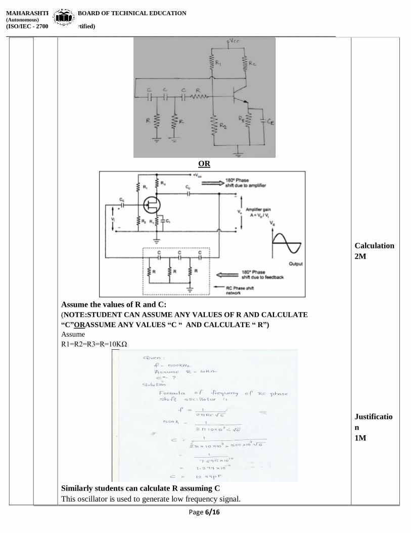
d) Design a RC phase shift oscillator to generate the frequency of 500KHz.Assume
suitable values for R1=R2=R3=R and C1=C2=C3=C .Justifyyour answer. 4M
Ans: RC Phase shift oscillator: Circuit
diagram
1M
MAHARASHTRA STATE BOARD OF TECHNICAL EDUCATION (Autonomous)
(ISO/IEC - 27001 - 2013 Certified)
__________________________________________________________________________________________________
Page 6/16
OR
Assume the values of R and C:
(NOTE:STUDENT CAN ASSUME ANY VALUES OF R AND CALCULATE
“C”ORASSUME ANY VALUES “C “ AND CALCULATE “ R”)
Assume
R1=R2=R3=R=10KΩ
Similarly students can calculate R assuming C
This oscillator is used to generate low frequency signal.
Calculation
2M
Justificatio
n
1M
MAHARASHTRA STATE BOARD OF TECHNICAL EDUCATION (Autonomous)
(ISO/IEC - 27001 - 2013 Certified)
__________________________________________________________________________________________________
Page 7/16
Q.3 Attempt any THREE of the following: 12-Total
Marks
a) Classify the power amplifiers on the basis of operation and input/output
waveforms. 4M
Ans: Depending upon the operation and input/output waveforms power amplifiers are
classified into following type.
1) Class A amplifier.
2) Class B amplifier.
3) Class C amplifier.
4) Class AB amplifier.
5) Class D amplifier.
Any 4 types
1M each
b) Describe the operation of class-C type of power amplifier with the help of neat
sketch. 4M
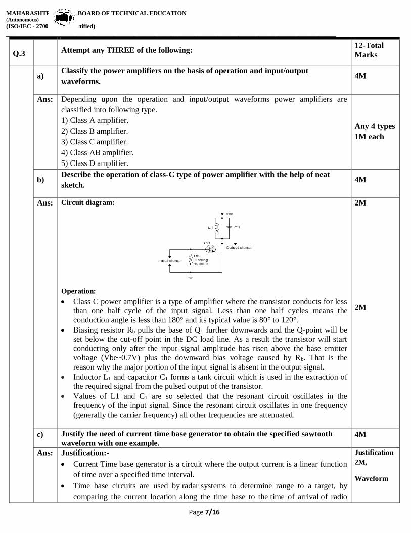
Ans: Circuit diagram:
Operation:
Class C power amplifier is a type of amplifier where the transistor conducts for less
than one half cycle of the input signal. Less than one half cycles means the
conduction angle is less than 180° and its typical value is 80° to 120°.
Biasing resistor Rb pulls the base of Q1 further downwards and the Q-point will be
set below the cut-off point in the DC load line. As a result the transistor will start
conducting only after the input signal amplitude has risen above the base emitter
voltage (Vbe~0.7V) plus the downward bias voltage caused by Rb. That is the
reason why the major portion of the input signal is absent in the output signal.
Inductor L1 and capacitor C1 forms a tank circuit which is used in the extraction of
the required signal from the pulsed output of the transistor.
Values of L1 and C1 are so selected that the resonant circuit oscillates in the
frequency of the input signal. Since the resonant circuit oscillates in one frequency
(generally the carrier frequency) all other frequencies are attenuated.
2M
2M
c) Justify the need of current time base generator to obtain the specified sawtooth
waveform with one example. 4M
Ans: Justification:-
Current Time base generator is a circuit where the output current is a linear function
of time over a specified time interval.
Time base circuits are used by radar systems to determine range to a target, by
comparing the current location along the time base to the time of arrival of radio
Justification
2M,
Waveform
MAHARASHTRA STATE BOARD OF TECHNICAL EDUCATION (Autonomous)
(ISO/IEC - 27001 - 2013 Certified)
__________________________________________________________________________________________________
Page 8/16
echoes.
Current Time base generators produce very high frequency sawtooth
waves specifically designed to deflect the beam in cathode ray tube (CRT) smoothly
across the face of the tube and then return it to its starting position.
To display the variations of a signal with respect to time on an oscilloscope, a
voltage/current that varies linearly with time, has to be applied to the deflection
plates. This makes the signal to sweep the beam horizontally
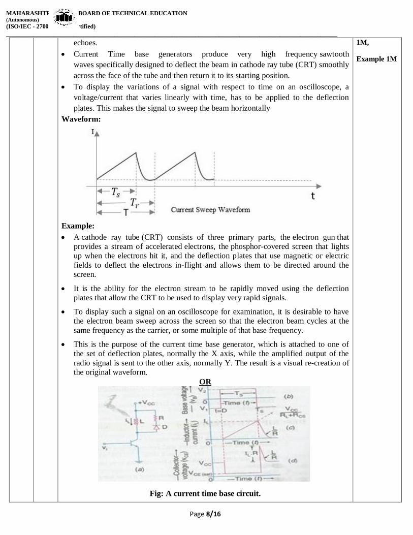
Waveform:
Example:
A cathode ray tube (CRT) consists of three primary parts, the electron gun that
provides a stream of accelerated electrons, the phosphor-covered screen that lights
up when the electrons hit it, and the deflection plates that use magnetic or electric
fields to deflect the electrons in-flight and allows them to be directed around the
screen.
It is the ability for the electron stream to be rapidly moved using the deflection
plates that allow the CRT to be used to display very rapid signals.
To display such a signal on an oscilloscope for examination, it is desirable to have
the electron beam sweep across the screen so that the electron beam cycles at the
same frequency as the carrier, or some multiple of that base frequency.
This is the purpose of the current time base generator, which is attached to one of
the set of deflection plates, normally the X axis, while the amplified output of the
radio signal is sent to the other axis, normally Y. The result is a visual re-creation of
the original waveform.
OR
Fig: A current time base circuit.
1M,
Example 1M
MAHARASHTRA STATE BOARD OF TECHNICAL EDUCATION (Autonomous)
(ISO/IEC - 27001 - 2013 Certified)
__________________________________________________________________________________________________
Page 9/16
Above Fig. shows a simple circuit of a current time base generator.
Here an inductor (L) in series with a transistor is connected across the VCC supply.
The transistor operates as a switch in the circuit.
The gating waveform at the base operates between two levels. V1and V2 as
shown.
The lower level (V1) keeps the transistor in cut-off, while the upper level drives
the transistor into saturation.
When the transistor switch is turned ON, then neglecting the effect of small
saturation resistance (Rcs), the current through and inductor (iL) increases linearly
with the time.
The diode D does not conduct during the sweep, because it is reverse biased.
d) Design a voltage regulator using IC LM317, draw the circuit diagram and state the
output voltage equation. 4M
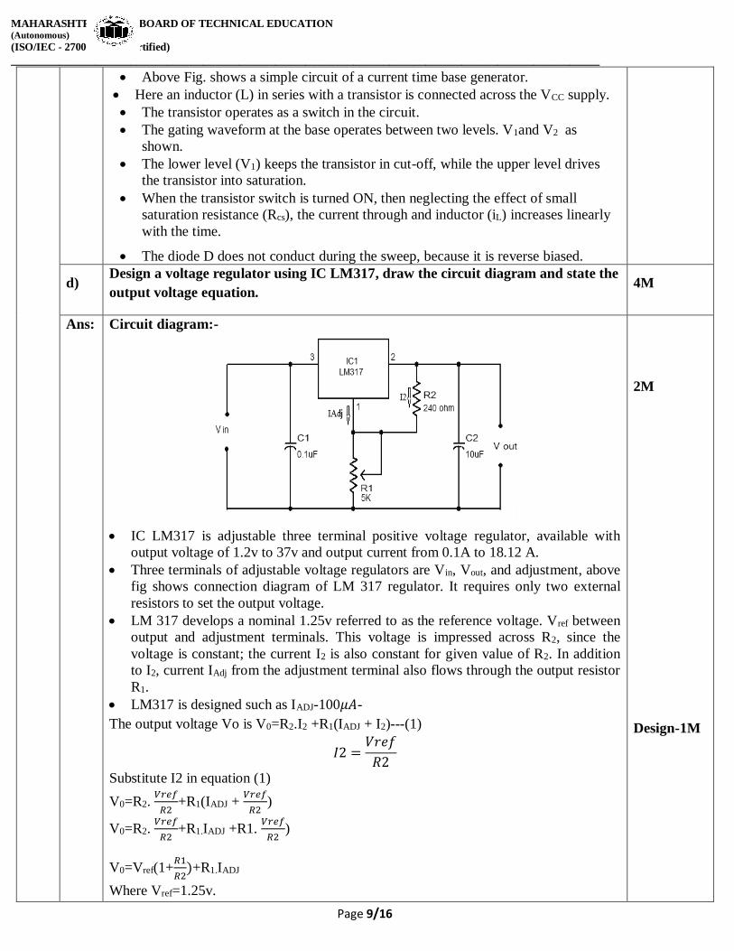
Ans: Circuit diagram:-
IC LM317 is adjustable three terminal positive voltage regulator, available with
output voltage of 1.2v to 37v and output current from 0.1A to 18.12 A.
Three terminals of adjustable voltage regulators are Vin, Vout, and adjustment, above
fig shows connection diagram of LM 317 regulator. It requires only two external
resistors to set the output voltage.
LM 317 develops a nominal 1.25v referred to as the reference voltage. Vref between
output and adjustment terminals. This voltage is impressed across R2, since the
voltage is constant; the current I2 is also constant for given value of R2. In addition
to I2, current IAdj from the adjustment terminal also flows through the output resistor
R1.
LM317 is designed such as IADJ-100𝜇𝐴-
The output voltage Vo is V0=R2.I2 +R1(IADJ + I2)---(1)
𝐼2 =𝑉𝑟𝑒𝑓
𝑅2
Substitute I2 in equation (1)
V0=R2. 𝑉𝑟𝑒𝑓
𝑅2+R1(IADJ +
𝑉𝑟𝑒𝑓
𝑅2)
V0=R2. 𝑉𝑟𝑒𝑓
𝑅2+R1.IADJ +R1.
𝑉𝑟𝑒𝑓
𝑅2)
V0=Vref(1+𝑅1
𝑅2)+R1.IADJ
Where Vref=1.25v.
2M
Design-1M
MAHARASHTRA STATE BOARD OF TECHNICAL EDUCATION (Autonomous)
(ISO/IEC - 27001 - 2013 Certified)
__________________________________________________________________________________________________
Page 10/16
However the current IADJ is very small and constant. Therefore the voltage drop across
R2 due to IADJ is also very small and can be neglected.
Therefore
V0=1.25.(1+𝑹𝟏
𝑹𝟐)
The output is a function of R1 for a given value of R2 and can be varied by adjusting the
value of R1. The resistor R2 usually is 240 ohm. Normally no capacitor is needed unless
the LM317 is situated far from the power supply filter capacitor.
Output
equation-
1M
Q.4
Attempt any THREE of the following : 12-Total
Marks
a) Draw the two stage BJT amplifier. State the formula for overall gain of this amplifier.
4M
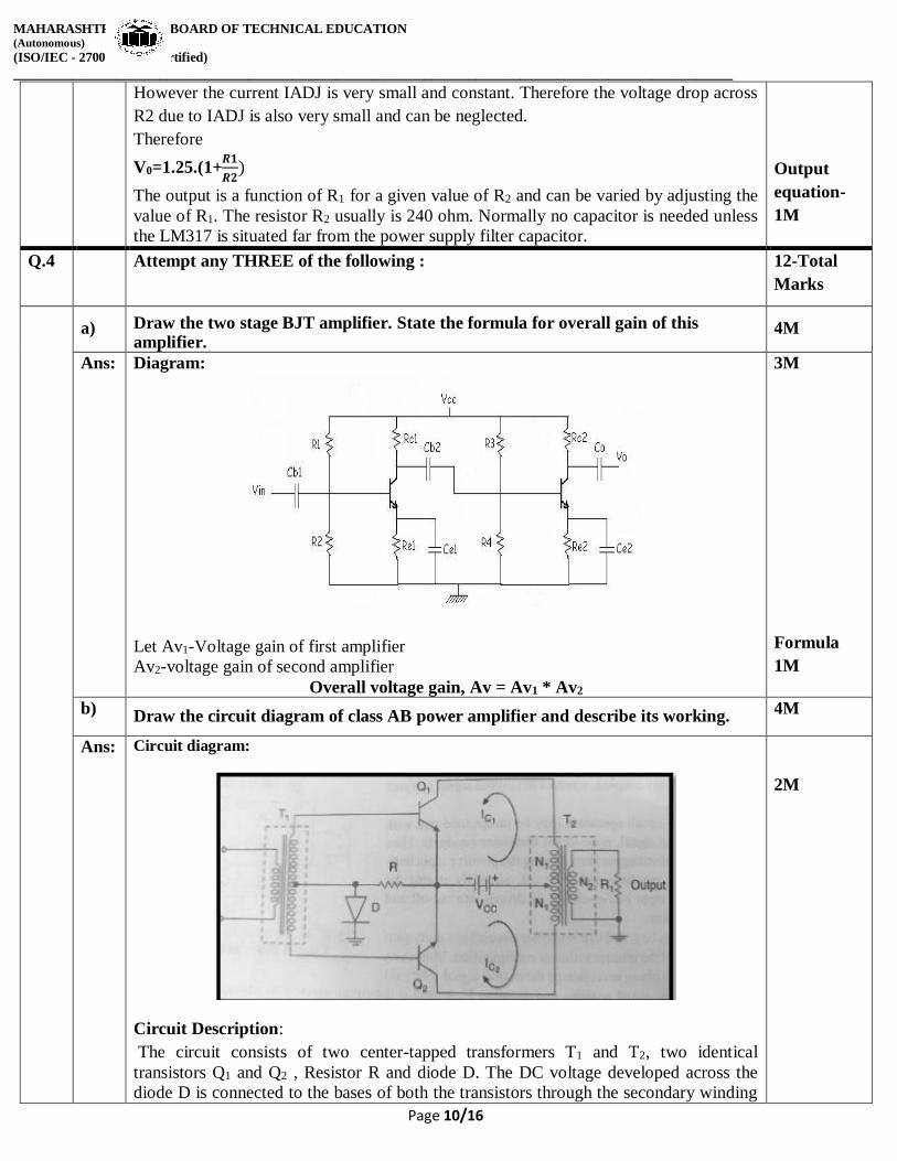
Ans: Diagram:
Let Av1-Voltage gain of first amplifier
Av2-voltage gain of second amplifier
Overall voltage gain, Av = Av1 * Av2
3M
Formula
1M
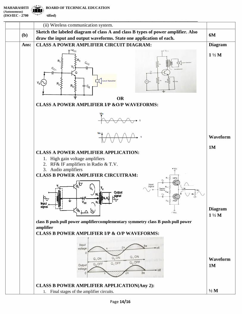
b) Draw the circuit diagram of class AB power amplifier and describe its working. 4M
Ans: Circuit diagram:
Circuit Description:
The circuit consists of two center-tapped transformers T1 and T2, two identical
transistors Q1 and Q2 , Resistor R and diode D. The DC voltage developed across the
diode D is connected to the bases of both the transistors through the secondary winding
2M
MAHARASHTRA STATE BOARD OF TECHNICAL EDUCATION (Autonomous)
(ISO/IEC - 27001 - 2013 Certified)
__________________________________________________________________________________________________
Page 11/16
of the input transformer. This voltage acts as DC bias for the transistors because it is
equal to cut-in voltage and they will conduct for complete half cycleperiod of the input
to eliminate the cross-over distortion.
WORKING:
i. When there is no a.c. input signal is applied both the transistors Q1& Q2 are cut
off. Hence no current is drawn from VCC.
ii. DURING POSITIVE HALF CYCLE:
The base of the transistor Q1 is positive and that of Q2 is negative.
iii. As a result of this Q1 conducts, while the transistor Q2 is OFF. DURING
DURING NEGATIVE HALF CYCLE:
The base of the transistor Q2 is positive and that of Q1 is negative.
As a result of this Q2 conducts, while the transistor Q1 is OFF.
iv. Thus at any instant any one transistor in the circuit is conducting. Then the
output transformer joins these two halves & produces a full sine wave in the load
resistor.
OR
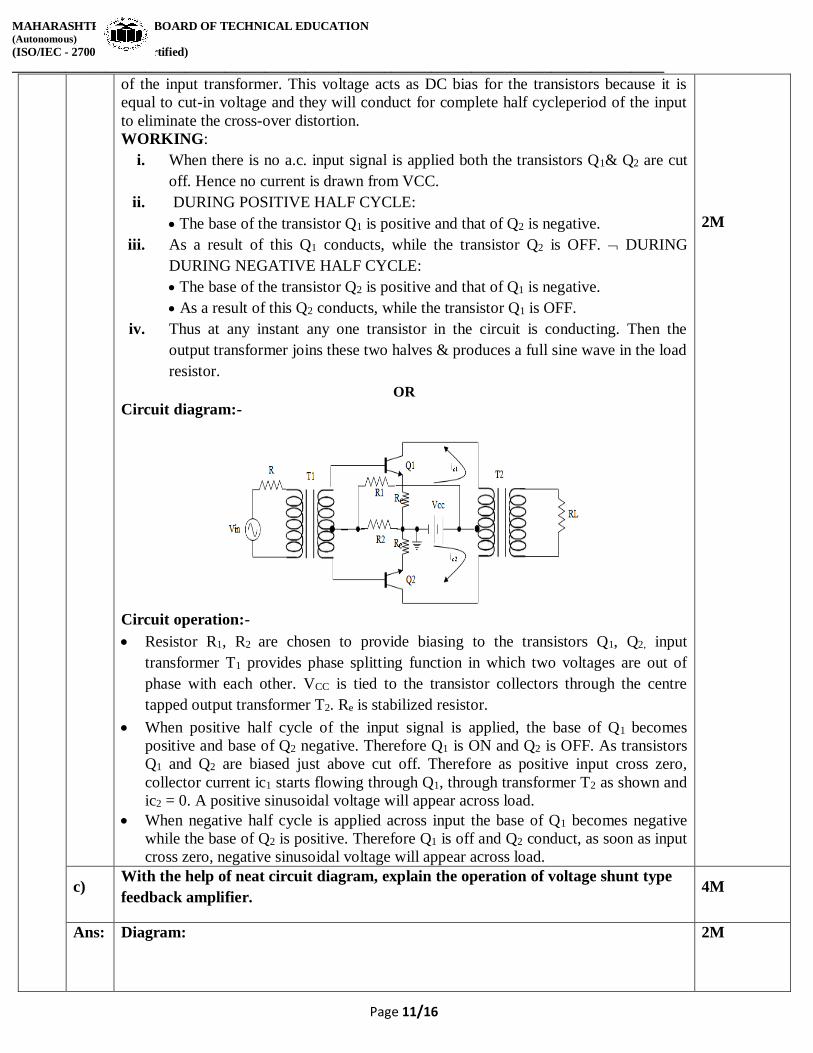
Circuit diagram:-
Circuit operation:-
Resistor R1, R2 are chosen to provide biasing to the transistors Q1, Q2, input
transformer T1 provides phase splitting function in which two voltages are out of
phase with each other. VCC is tied to the transistor collectors through the centre
tapped output transformer T2. Re is stabilized resistor.
When positive half cycle of the input signal is applied, the base of Q1 becomes
positive and base of Q2 negative. Therefore Q1 is ON and Q2 is OFF. As transistors
Q1 and Q2 are biased just above cut off. Therefore as positive input cross zero,
collector current ic1 starts flowing through Q1, through transformer T2 as shown and
ic2 = 0. A positive sinusoidal voltage will appear across load.
When negative half cycle is applied across input the base of Q1 becomes negative
while the base of Q2 is positive. Therefore Q1 is off and Q2 conduct, as soon as input
cross zero, negative sinusoidal voltage will appear across load.
2M
c) With the help of neat circuit diagram, explain the operation of voltage shunt type
feedback amplifier. 4M
Ans: Diagram: 2M
MAHARASHTRA STATE BOARD OF TECHNICAL EDUCATION (Autonomous)
(ISO/IEC - 27001 - 2013 Certified)
__________________________________________________________________________________________________
Page 12/16
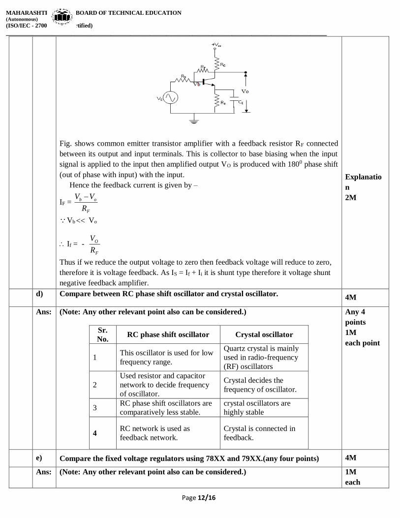
Fig. shows common emitter transistor amplifier with a feedback resistor RF connected
between its output and input terminals. This is collector to base biasing when the input
signal is applied to the input then amplified output VO is produced with 1800 phase shift
(out of phase with input) with the input.
Hence the feedback current is given by –
IF = F
ob
R
VV
Vb Vo
If = - F
O
R
V
Thus if we reduce the output voltage to zero then feedback voltage will reduce to zero,
therefore it is voltage feedback. As IS = If + Ii it is shunt type therefore it voltage shunt
negative feedback amplifier.
Explanatio
n
2M
d) Compare between RC phase shift oscillator and crystal oscillator.
4M
Ans: (Note: Any other relevant point also can be considered.)
Sr.
No. RC phase shift oscillator Crystal oscillator
1 This oscillator is used for low
frequency range.
Quartz crystal is mainly
used in radio-frequency
(RF) oscillators
2
Used resistor and capacitor
network to decide frequency
of oscillator.
Crystal decides the
frequency of oscillator.
3 RC phase shift oscillators are
comparatively less stable.
crystal oscillators are
highly stable
4 RC network is used as
feedback network.
Crystal is connected in
feedback.
Any 4
points
1M
each point
e) Compare the fixed voltage regulators using 78XX and 79XX.(any four points) 4M
Ans: (Note: Any other relevant point also can be considered.)
1M
each
MAHARASHTRA STATE BOARD OF TECHNICAL EDUCATION (Autonomous)
(ISO/IEC - 27001 - 2013 Certified)
__________________________________________________________________________________________________
Page 13/16
Sr.
No. 78xx 79xx
1 It produces positive fixed
DC voltage values,
It produces negative
fixed DC voltage values
2
IC 78xx (7805, 7806, 7808,
7812, 7815, 7818,7824)-
Positive Voltage Regulator.
IC 79xx (7905,
7906,7908,7912, 7915) -
Negative Voltage
Regulator
3 Output current is 1A Output current is 1.5A
4 OR
1-Input
2-Ground
3-Output
OR
1-Ground
2-Input
3-Output
point
Q.5
Attempt any TWO of the following 12
Total
Marks
(a) Describe the operation of double tuned amplifier with the help of neat circuit
diagram and mention its applications. 6M
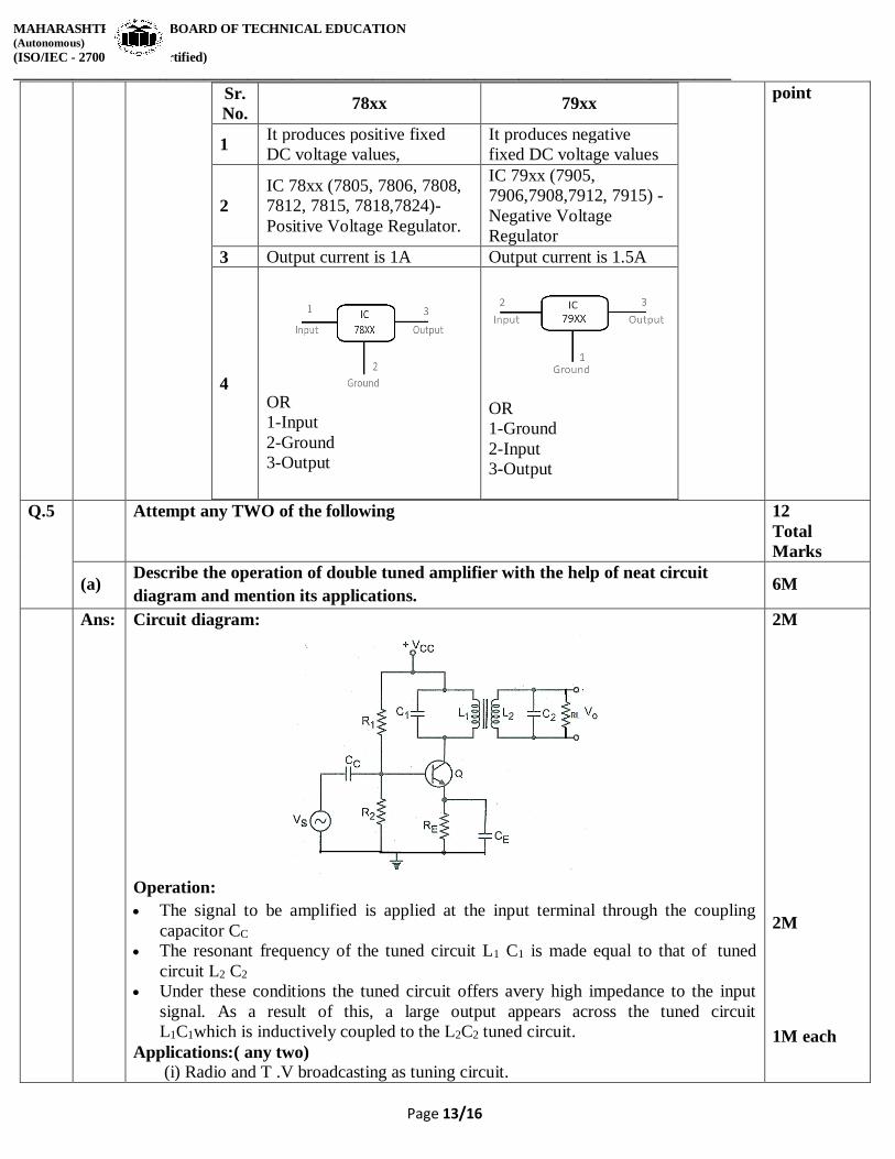
Ans: Circuit diagram:
Operation:
The signal to be amplified is applied at the input terminal through the coupling
capacitor CC
The resonant frequency of the tuned circuit L1 C1 is made equal to that of tuned
circuit L2 C2
Under these conditions the tuned circuit offers avery high impedance to the input
signal. As a result of this, a large output appears across the tuned circuit
L1C1which is inductively coupled to the L2C2 tuned circuit.
Applications:( any two)
(i) Radio and T .V broadcasting as tuning circuit.
2M
2M
1M each
MAHARASHTRA STATE BOARD OF TECHNICAL EDUCATION (Autonomous)
(ISO/IEC - 27001 - 2013 Certified)
__________________________________________________________________________________________________
Page 14/16
(ii) Wireless communication system.
(b) Sketch the labeled diagram of class A and class B types of power amplifier. Also
draw the input and output waveforms. State one application of each. 6M
Ans: CLASS A POWER AMPLIFIER CIRCUIT DIAGRAM:
OR
CLASS A POWER AMPLIFIER I/P &O/P WAVEFORMS:
CLASS A POWER AMPLIFIER APPLICATION:
1. High gain voltage amplifiers
2. RF& IF amplifiers in Radio & T.V.
3. Audio amplifiers
CLASS B POWER AMPLIFIER CIRCUITRAM:
class B push pull power amplifiercomplementary symmetry class B push pull power
amplifier
CLASS B POWER AMPLIFIER I/P & O/P WAVEFORMS:
CLASS B POWER AMPLIFIER APPLICATION(Any 2):
1. Final stages of the amplifier circuits.
Diagram
1 ½ M
Waveform
1M
Diagram
1 ½ M
Waveform
1M
½ M
MAHARASHTRA STATE BOARD OF TECHNICAL EDUCATION (Autonomous)
(ISO/IEC - 27001 - 2013 Certified)
__________________________________________________________________________________________________
Page 15/16
2. In public address systems (PA system)
3. In tape recorders and music system
4. In T.V receivers
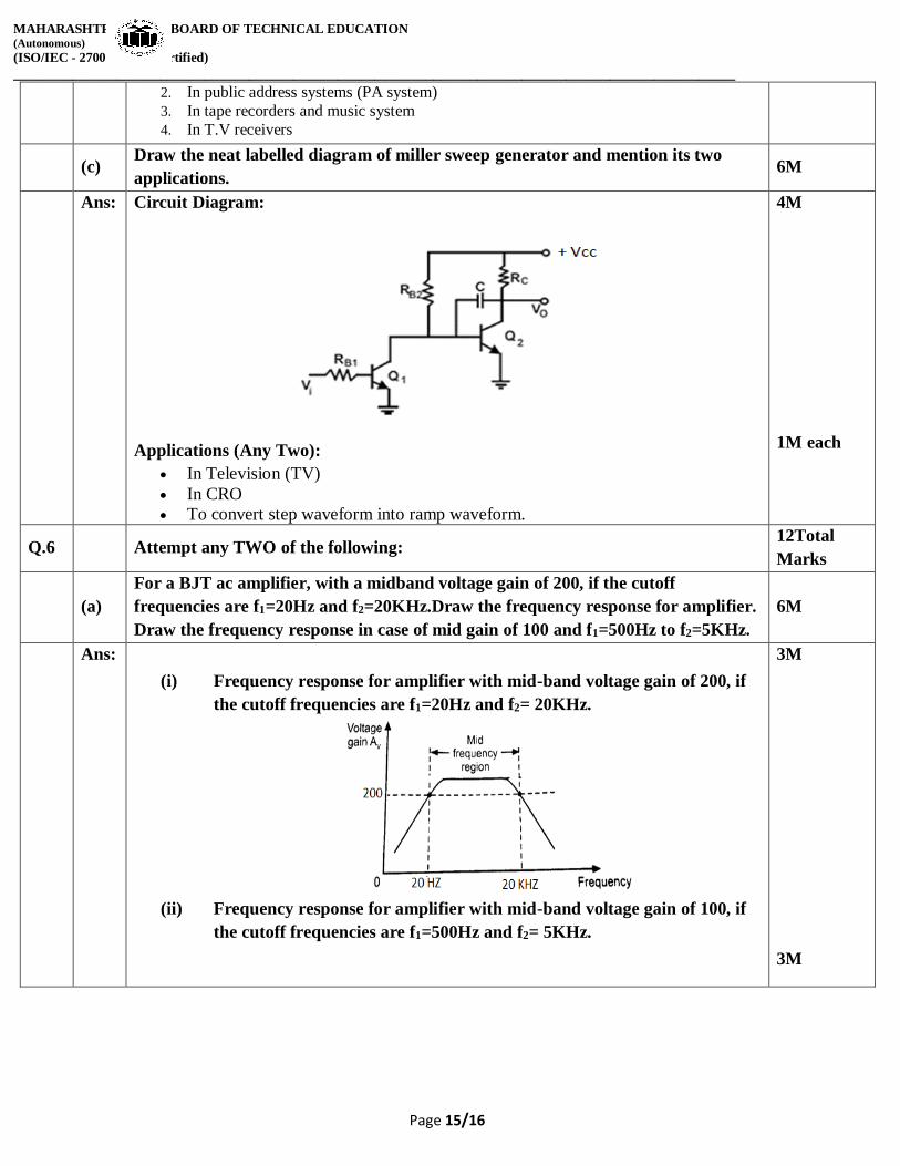
(c) Draw the neat labelled diagram of miller sweep generator and mention its two
applications. 6M
Ans: Circuit Diagram:
Applications (Any Two):
In Television (TV)
In CRO
To convert step waveform into ramp waveform.
4M
1M each
Q.6 Attempt any TWO of the following: 12Total
Marks
(a)
For a BJT ac amplifier, with a midband voltage gain of 200, if the cutoff
frequencies are f1=20Hz and f2=20KHz.Draw the frequency response for amplifier.
Draw the frequency response in case of mid gain of 100 and f1=500Hz to f2=5KHz.
6M
Ans:
(i) Frequency response for amplifier with mid-band voltage gain of 200, if
the cutoff frequencies are f1=20Hz and f2= 20KHz.
(ii) Frequency response for amplifier with mid-band voltage gain of 100, if
the cutoff frequencies are f1=500Hz and f2= 5KHz.
3M
3M
MAHARASHTRA STATE BOARD OF TECHNICAL EDUCATION (Autonomous)
(ISO/IEC - 27001 - 2013 Certified)
__________________________________________________________________________________________________
Page 16/16
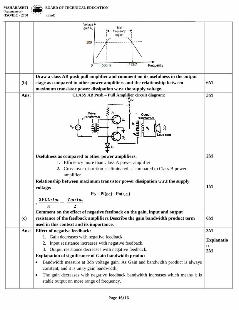
(b)
Draw a class AB push pull amplifier and comment on its usefulness in the output
stage as compared to other power amplifiers and the relationship between
maximum transistor power dissipation w.r.t the supply voltage.
6M
Ans: CLASS AB Push – Pull Amplifier circuit diagram:
Usefulness as compared to other power amplifiers:
1. Efficiency more than Class A power amplifier
2. Cross over distortion is eliminated as compared to Class B power
amplifier.
Relationship between maximum transistor power dissipation w.r.t the supply
voltage:
PD = Pi(DC)– Po(A.C.)
=
𝟐𝑽𝑪𝑪∗𝑰𝒎
𝝅−
𝑽𝒎∗𝑰𝒎
𝟐
3M
2M
1M
(c)
Comment on the effect of negative feedback on the gain, input and output
resistance of the feedback amplifiers.Describe the gain bandwidth product term
used in this context and its importance.
6M
Ans: Effect of negative feedback:
1. Gain decreases with negative feedback.
2. Input resistance increases with negative feedback.
3. Output resistance decreases with negative feedback.
Explanation of significance of Gain bandwidth product
Bandwidth measure at 3db voltage gain. As Gain and bandwidth product is always
constant, and it is unity gain bandwidth.
The gain decreases with negative feedback bandwidth increases which means it is
stable output on more range of frequency.
3M
Explanatio
n
3M


