Embed Size (px)
Citation preview
POWER ELECTRONIC TOPOLOGIES WITH HIGH DENSITY POWER
CONVERSION AND GALVANIC ISOLATION FOR UTILITY INTERFACE
A Dissertation
by
HARISH SARMA KRISHNAMOORTHY
Submitted to the Office of Graduate and Professional Studies of
Texas A&M University
in partial fulfillment of the requirements for the degree of
DOCTOR OF PHILOSOPHY
Chair of Committee, Prasad N. Enjeti Committee Members, Hamid A. Toliyat
Shankar P. Bhattacharyya
Won-jong Kim
Head of Department, Chanan Singh
May 2015
Major Subject: Electrical Engineering
Copyright 2015 Harish Sarma Krishnamoorthy

ii
ABSTRACT
The past decade has seen a significant increase in the number of applications
where power electronic converters play a major role. Renewable energy systems such as
wind turbines, solar photovoltaics, etc. employ power converters to interface with the
utility grid. More and more power converters are being used in transportation sector such
as in electric vehicles, locomotives, aircrafts, ships and submarines. Advancements in
power converter topologies and devices have constantly pushed the limits and standards
applicable in different markets towards better efficiency, lower cost and higher power
density. Especially for large power systems such as wind turbine generators, adjustable
speed drives, locomotives, etc., achieving smaller footprint at low cost and high
efficiency has become a major challenge. These factors generate the major impetus
towards the research undertaken in this dissertation.
In applications that require integration with the utility grid, the bulkiest
components are usually the transformers, inductors and DC electrolytic capacitors.
Instead of using a line frequency transformer to interface any power electronic system
with the utility grid directly, it is possible to use a power converter to transform the line
frequency AC into a higher frequency AC that can be fed to a medium or high frequency
transformer. These transformers are much smaller and lighter compared to line
frequency transformers. This dissertation elucidates these concepts in detail in the first
section as well as at the beginning of each subsequent section, along with a summary of
such techniques already proposed in the literature.

iii
The sections in this dissertation propose and discuss several architectures
(approaches) adhering to the earlier stated concepts that enable higher power density
energy conversion for applications such as wind turbines, adjustable speed drives, data
centers, energy storage systems, etc. Detailed operational analysis, design example,
control strategy, simulation results and experimental results are shown for each concept
or topology. The advantages and drawbacks are also discussed.
Finally in this dissertation, the medium or high frequency transformers that can
be used in the proposed approaches are analyzed in detail using ANSYS Maxwell
software in terms of material, saturation, loss and size. Further, these numbers are used
to estimate the relative size advantage and efficiency that can be achieved using higher
frequency transformer compared to a line frequency transformer for utility interface
applications. It will be shown that for many high power applications, medium frequency
transformer based circuit designs can be more efficient and simpler alternatives for high
frequency transformer based approaches. The specific contributions along with future
research opportunities of the proposed concepts are summarized at the end.

iv
ACKNOWLEDGEMENTS
I do not have enough words to thank my advisor, Dr. Prasad N. Enjeti for
imparting knowledge and molding me into a researcher that I am today. He has not only
been a wonderful guide to me, but also a patient mentor with whom I always enjoyed
having long discussions about engineering, professional career, and other aspects of life,
throughout my graduate study. I feel privileged to have a PhD committee involving very
eminent professors in Dr. Hamid A. Toliyat, Dr. Shankar P. Bhattacharyya and Dr. Won-
jong Kim. I extend my sincere gratitude for their insight, guidance and time spent for
me. I also thank the Qatar National Research Foundation for their support. I thank the
Texas A&M ECE department staff, especially Tammy Carda, Jeanie Marshall, Annie
Brunker, among all others who helped me immensely during my life at graduate school.
I should also acknowledge and thank my professors and teachers from my earlier years
in undergraduate university and high school for providing the foundation necessary to
accomplish this work.
I would like to acknowledge all current and past students in the research group
and in Texas A&M power electronics division, without whom my work would have
been very hard. I thank (in no particular order) Somasundaram Essakiappan, Pawan
Garg, Poornima Mazumdar, Joshua Hawke, Dibyendu Rana, Jorge Ramos, Jose
Sandoval, Michael Daniel, Taeyong Kang, Bahaa Hafez, Ahmed Morsy, Vivek
Sundaram, Yateendra Deshpande, Souhib Harb, Mohammad Shadmand and all others in
the EPPE research division for making learning and life enjoyable.

v
I extend my gratitude to all my colleagues from GE, Ford, Schlumberger and
Google, where I have worked/interned at different points of time, for providing me with
a deep knowledge of their respective industry. I would also like to thank organizations
such as ABB, Magna-Power, etc. for providing valuable support to my research through
funds, facilities or services.
Last but not least, I thank my wife, Tulasi, my parents, brother, in-laws, relatives
and friends for believing in me, supporting me and also for boosting my morale when
the chips were down.
vi
TABLE OF CONTENTS
Page
ABSTRACT ...................................................................................................................... ii
ACKNOWLEDGEMENTS ..............................................................................................iv
TABLE OF CONTENTS ..................................................................................................vi
LIST OF FIGURES ...........................................................................................................ix
LIST OF TABLES ..........................................................................................................xvi
1. INTRODUCTION ...................................................................................................... 1
1.1. Introduction ......................................................................................................... 1 1.2. Applications Involving Utility Interface .............................................................. 2 1.3. Power Density and Power-to-Mass Ratio of Converters ..................................... 3
1.3.1. Components Affecting Power Density ......................................................... 5 1.3.2. Methods to Improve Converter Power Density ............................................ 6 1.3.3. Medium or High Frequency Transformer .................................................... 7
1.4. Power Converter Modelling and Implementation ............................................... 8
1.5. Research Objective ............................................................................................ 13 1.6. Outline of Dissertation ....................................................................................... 15
2. HIGH POWER AC-DC CONVERTER WITH BOOST PFC ................................. 18
2.1. Isolated AC-DC converters ............................................................................... 18 2.2. Proposed 3-phase Isolated AC-DC Converter Topology .................................. 23
2.2.1. AC-AC Converter ...................................................................................... 23 2.2.2. Medium or High Frequency Transformer .................................................. 24 2.2.3. 1-phase Boost PFC Stage ........................................................................... 27 2.2.4. Control Strategy ......................................................................................... 28
2.3. Size and Loss Comparison ................................................................................ 30 2.4. Simulation and Experimental Results ................................................................ 31 2.5. Conclusion ......................................................................................................... 37
3. SIMPLIFIED MEDIUM/HIGH FREQUENCY TRANSFORMER BASED
MULTI-PULSE DIODE RECTIFIERS ........................................................................... 38
Introduction to Adjustable Speed Drives and Multi-Pulse Rectifiers ............... 38 3.1.
12-pulse Rectifier using Higher Frequency Transformer .................................. 42 3.2.
3.2.1. AC – AC Converter and Modulation Scheme ............................................ 47
vii
3.2.2. 3-Phase Diode Rectifier (for 12-pulse configuration) ................................ 49 3.2.3. Medium Frequency (MF) or High Frequency (HF) Transformer .............. 51 3.2.4. Passive Components and Filter Design ...................................................... 51 3.2.5. Simulation Results ...................................................................................... 52 3.2.6. Experimental Results .................................................................................. 54
MF Transformer based ASD Topology with PWM Front-End ......................... 57 3.3.
3.3.1. AC-AC Converter Operation ..................................................................... 58 3.3.2. Three-Phase Diode Rectifier ...................................................................... 60 3.3.3. Medium Frequency Transformer ............................................................... 62 3.3.4. ASD with Motor Drive Inverter ................................................................. 62
3.3.5. Simulation Results ...................................................................................... 63 3.3.6. Experimental Results .................................................................................. 64
Conclusion ......................................................................................................... 65 3.4.
4. A NEW WIND TURBINE – MEDIUM VOLTAGE DC (MVDC)
INTERCONNECTION .................................................................................................... 67
4.1. Introduction to Wind Turbine Generators (WTGs) ........................................... 67 4.2. Introduction to Offshore Wind Farms ............................................................... 68 4.3. State of the Art ................................................................................................... 69 4.4. A New WTG-MVDC Interconnection using 3-level Boost PFC ...................... 73
4.4.1. AC-AC Converter ...................................................................................... 74 4.4.2. Single Phase 3-level Boost PFCs ............................................................... 74 4.4.3. Control Strategy ......................................................................................... 76 4.4.4. Medium Frequency (MF) Transformer ...................................................... 77 4.4.5. Filter Design ............................................................................................... 77
4.5. Maximum Power Point Tracking (MPPT) ........................................................ 78 4.6. Simulation .......................................................................................................... 80 4.7. Conclusion ......................................................................................................... 84
5. WIND TURBINE - BATTERY ENERGY STORAGE UTILITY
INTERFACE WITH MEDIUM FREQUENCY TRANSFORMER ............................... 86
5.1. Introduction to Energy Storage in Renewable Energy Systems ........................ 86 5.2. Proposed Battery Energy Storage - Utility Interface Converter ........................ 89
5.2.1. Multi-Level AC-AC Converter .................................................................. 90 5.2.2. Battery Energy Storage System (BESS) .................................................... 90 5.2.3. 3-Phase PWM Rectifier/Inverter ................................................................ 91 5.2.4. Medium Frequency (MF) Transformer ...................................................... 92 5.2.5. Control Strategy ......................................................................................... 93
5.3. Proposed WTG-BESS Utility Interface Converter in 3-port
Configuration ............................................................................................................... 95
viii
5.3.1. Multi-Level AC-AC Converter .................................................................. 98 5.3.2. Wind Turbine Generator (WTG) and Battery Energy Storage
System (BESS) ......................................................................................................... 98 5.3.3. 3-Phase PWM Rectifier and Inverter ......................................................... 99 5.3.4. Medium Frequency (MF) Transformer ...................................................... 99 5.3.5. Control Strategy ......................................................................................... 99
5.4. Low Voltage Ride Through (LVRT) Capability ............................................. 101 5.5. Simulation Results ........................................................................................... 104 5.6. Experimental Results ....................................................................................... 110 5.7. Conclusion ....................................................................................................... 114
6. MEDIUM AND HIGH FREQUENCY TRANSFORMER DESIGN AND
SYSTEM ANALYSIS ................................................................................................... 116
6.1. Design of Higher Frequency Transformers for High Power Applications ...... 116 6.2. Magnetization Characteristics of Different Transformer Core Materials ....... 119 6.3. Analysis of core losses at different voltage waveforms .................................. 121 6.4. Example Design of Transformers for the Proposed Topologies ..................... 123 6.5. Maxwell Simulations of Different Transformer Designs ................................ 128
6.5.1. M19 Silicon Steel Core with 600 Hz Base Operating Frequency ............ 128 6.5.2. M19 Silicon Steel Core with 60 Hz Base Operating Frequency .............. 129
6.5.3. Metglass 2605 Core with 600 Hz and 6 kHz Base Operating
Frequencies ............................................................................................................. 130 6.5.4. Ferrite 3C85 Core with 6 kHz Base Operating Frequency ...................... 132
6.6. Inference and Conclusion ................................................................................ 133
7. SUMMARY ........................................................................................................... 140
7.1. Conclusion ....................................................................................................... 140 7.2. Future Work ..................................................................................................... 142
REFERENCES ............................................................................................................... 143
ix
LIST OF FIGURES
Page
Figure 1-1: Capacity and generation expansion in low-demand as baseline
(Adapted with permission from the US National Renewable Energy
Laboratory [1]) ....................................................................................................... 2
Figure 1-2: Distributed energy sources (Adapted with permission from the US
National Renewable Energy Laboratory [4]) ......................................................... 3
Figure 1-3: Electric locomotive and offshore wind turbines [8-10] (Adapted with
permission from the National Institute of Standards and Technology, U.S.
Dept. of Commerce [10]) ....................................................................................... 4
Figure 1-4: Volume of components in a 10 kW DC-AC converter (© 2013 IEEE
[11] – Adapted with permission from the IEEE) ................................................... 5
Figure 1-5: Volume comparison of different transformer designs (© 2010 IEEE
[14] – Adapted with permission from the IEEE) ................................................... 7
Figure 1-6: Square wave switching function for DC input ................................................ 9
Figure 1-7: High frequency square wave switching function for low frequency
sinusoidal input .................................................................................................... 10
Figure 1-8: High frequency sine PWM switching function for low frequency
sinusoidal input .................................................................................................... 11
Figure 1-9: Sinusoidal PWM switching function – bipolar and unipolar versions .......... 12
Figure 1-10: AC-AC converter evolution – bidirectional (with / without
bidirectional switches) to unidirectional .............................................................. 12
Figure 2-1: AC-DC converter with a 3-phase diode rectifier front-end and an
isolated DC-DC converter .................................................................................... 19
Figure 2-2: A high power AC-DC approach using three 1-phase PFC-DC-DC
converter stages. ................................................................................................... 19
Figure 2-3: Vienna rectifier front-end based isolated AC-DC converter ......................... 21
Figure 2-4: Proposed AC-DC converter with three 1-phase MF/HF transformers
and boost PFC circuits (three DC outputs, Vdc,A, Vdc,B and Vdc,C of the
boost PFC stages can be connected in series or parallel as required for the
application) ........................................................................................................... 22
x
Figure 2-5: Proposed converter with a single 3-phase transformer instead of three
1-phase transformers ............................................................................................ 26
Figure 2-6: Single-phase equivalent circuit with control system for the proposed
topology (Figure 2-4) ........................................................................................... 28
Figure 2-7: Simulation waveforms of the transformer primary side of the
proposed topology - (a) Utility input phase-A voltage and current (scale
increased for better resolution of current); (b) Pulsating DC-link voltage
and current; and (c) Transformer primary phase-A voltage and current .............. 32
Figure 2-8: Simulation waveforms of the transformer secondary side of the
proposed topology with boost PFCs- (a) Transformer secondary phase-A
voltage and current (scale increased for better resolution of current); (b)
Rectified PFC pulsating DC-link voltage and current; and (c) Load DC
voltage and the three phase PFC inductor currents, phase shifted. ...................... 33
Figure 2-9: Experimental waveforms with 600 Hz transformer - (a) Utility input
voltage Va, (b) Utility input current Ia, (c) Output DC voltage Vdc, (d)
Transformer primary voltage Vpri,A, and (e) Transformer current Ipri,A ................ 35
Figure 2-10: Experimental waveforms of the proposed topology with 600 Hz
transformer - (a) Utility input voltage Va, (b) Utility input current Ia, (c)
Output DC voltage Vdc ......................................................................................... 36
Figure 2-11: Experimental waveforms with 6 kHz transformer - (Ch. 1)
Transformer primary voltage Vpri,A, (Ch. 2) Secondary side rectified
voltage Vrect, (Ch. 3) Utility input current Ia, and (Ch. 4) Output DC
voltage Vdc ............................................................................................................ 37
Figure 3-1: Commercial motor drives (Note the bulky 60 Hz transformer and
diode bridge rectifiers) ......................................................................................... 39
Figure 3-2: Waveforms of the conventional 12-pulse rectifier topology shown in
Figure 1. ............................................................................................................... 41
Figure 3-3: Proposed MV-ASD topology with MF/HF isolation with 12-pulse
rectifier front-end ................................................................................................. 42
Figure 3-4: Proposed Medium Voltage ASD with series-stacked/cascaded AC-AC
converter structure ................................................................................................ 43
Figure 3-5: MF/HF Transformer based 18-pulse rectifier configuration ......................... 44
xi
Figure 3-6: Proposed medium voltage adjustable speed drive (MV ASD) topology
with medium frequency (MF) isolation with series-stacked inverter
modules in the transformers secondary (derived from [52]) ................................ 44
Figure 3-7: AC-AC Converter voltages and switching functions .................................... 47
Figure 3-8: (i) Input current and voltage (reduced scale) (ii) transformer primary
voltage and current; (iii) DC-link voltages .......................................................... 52
Figure 3-9: FFTs of waveforms in Figure 3-8 .................................................................. 53
Figure 3-10: Simulation waveforms at the transformer - (i) Primary voltage
(reduced scale) and current, (ii) Secondary and tertiary line-to-line
voltages; (iii) Secondary and tertiary diode rectifier input currents ..................... 54
Figure 3-11: Ch. (1), (2), (3) show the three transformer primary voltages and Ch.
(4) shows the unfiltered utility current ................................................................. 55
Figure 3-12: Experimental waveforms: DC bus voltage, transformer
secondary/tertiary voltages and filtered utility input current (Ch. 3) ................... 55
Figure 3-13: Experimental waveforms: individual DC bus voltages and utility
input current (Ch. 3) ............................................................................................. 56
Figure 3-14: ASD topology with PWM modulation at the front-end instead of
square wave. Note the unidirectional AC-AC converter (can be
constructed using bidirectional AC-AC converter also) ...................................... 58
Figure 3-15: AC-AC converter waveforms from Figure 3 topology. (a) Input grid
voltage and current, (b) Unipolar Sine PWM switching function, (c)
Square wave switching function and (d) Transformer secondary voltage ........... 60
Figure 3-16: (i) Utility voltage (Va), current (scaled), (ii) Transformer primary
voltage (Vpri,A) and current ................................................................................... 63
Figure 3-17: (i) Transformer secondary voltage (Vsec,A) and current (scaled); (ii)
DC bus voltage, (VDC) .......................................................................................... 64
Figure 3-18: Experimental results for the topology in Figure 3-14: (Ch1)
Transformer phase-A voltage, (Ch2) Transformer phase-B voltage, (Ch3)
DC voltage with inductive load ............................................................................ 65
Figure 4-1: Conventional WTG – utility grid interface using a line frequency
transformer ........................................................................................................... 68
xii
Figure 4-2: An example 400 MW offshore wind turbine generator architecture
with MVDC-HVDC interconnection ................................................................... 69
Figure 4-3: WTG Utility Interface with a line frequency transformer in 12-pulse
configuration ........................................................................................................ 69
Figure 4-4: Isolated Medium Frequency WTG-MVDC interconnection via DC-
DC converter ........................................................................................................ 72
Figure 4-5: Proposed WTG-MVDC interconnection using MF transformer and 3-
level boost PFC .................................................................................................... 73
Figure 4-6: Control strategy for the proposed approach in Figure 4-5 (shown only
phase-A) ............................................................................................................... 77
Figure 4-7: Equivalent diagram at the WTG for the filter design .................................... 77
Figure 4-8: Characteristics of pitch control in a 10 MVA WTG (© 2007 IEEE
[65] - Adapted with permission from the IEEE) .................................................. 79
Figure 4-9: PSIM Simulation waveforms at 100% WTG power and 15 m/s wind
speed ..................................................................................................................... 81
Figure 4-10: PSIM Simulation waveforms at 25% WTG power and 7 m/s wind
speed ..................................................................................................................... 82
Figure 4-11: Simulation waveforms of step change between 100% and 25% WTG
power (15 m/s to 7 m/s) ........................................................................................ 82
Figure 4-12: PSIM Simulation step change – boost PFC voltages .................................. 83
Figure 5-1: Medium voltage (or low voltage) utility - energy storage interface
topology with line frequency transformer and PWM Rectifier ............................ 87
Figure 5-2: Lower voltage utility - energy storage interface topology involving
high frequency transformer and two converter stages [73] .................................. 88
Figure 5-3: Proposed BESS - MV utility interface converter topology using MF
transformer isolation ............................................................................................ 89
Figure 5-4: Per-phase control strategy at the MF transformer of the proposed
topology for demand based power flow regulation among the grid and
BESS .................................................................................................................... 91
Figure 5-5: Idealized operating waveforms of the proposed system for battery
charging and discharging modes - (a) Battery voltage and current, (b) MF
xiii
transformer AC phase voltage and current, and (c) Input AC phase voltage
and current ............................................................................................................ 94
Figure 5-6: WTG Utility Interface with MF Transformer ............................................... 95
Figure 5-7: Wind Turbine Generator – Battery Energy Storage Converter 3-port
Configuration with Medium Frequency Transformer Isolation for Utility
Grid Integration .................................................................................................... 96
Figure 5-8: Per-phase control strategy at the MF transformer of the proposed
topology for demand based power flow regulation among the grid, WTG
and BESS (strategy similar for WTG as well as BESS side) ............................... 98
Figure 5-9: Energy Profile during conventional LVRT ................................................. 102
Figure 5-10: Conventional WTG Power Converter with chopper circuit for LVRT
Capability [83] .................................................................................................... 102
Figure 5-11: Energy profile during LVRT for the proposed topology with DC-link
chopper (bleeder) ................................................................................................ 102
Figure 5-12: Charging mode waveforms- (a) BESS current and voltage (for VBat =
800V, Ibat = -500A (b) WTG phase-A current and voltage (15Hz), (c)
Unfiltered utility grid phase-A current and 1/8th of utility voltage (scale
reduced for better resolution of current) and (d) Transformer secondary
current, tertiary current and cumulative primary phase-A voltage .................... 105
Figure 5-13: Discharging mode waveforms- (a) BESS current and voltage (for
VBat = 800V, Ibat = 800A (b) WTG phase-A current and voltage (15Hz),
(c) Unfiltered utility grid phase-A current and 1/8th of utility voltage and
(d) Transformer secondary current, tertiary current and cumulative
primary phase-A voltage .................................................................................... 106
Figure 5-14: (a) Transformer phase-A primary voltage, (b) Transformer phase-A
secondary voltage, (c) and (d) are respectively FFTs of (a) and (b) .................. 107
Figure 5-15: Variation in grid supply effected by WTG and BESS based on the
instantaneous power demand (a) BESS voltage and current, (b) WTG
voltage and current, and (c) Utility grid voltage and current (grid voltage
shown on a reduced scale for better resolution) ................................................. 108
Figure 5-16 (a): Voltage rise in the WTG DC-link capacitor during a temporary
line-to-ground fault in phase-A. chopper circuit operates when the DC-
Link voltage crosses 1800V. .............................................................................. 108
xiv
Figure 5-17: Utility voltages and currents in phase-B and phase-A during a line-
to-gnd fault in phase-A. ...................................................................................... 109
Figure 5-18: Control system performance under utility grid voltage swell and sag
– (a) BESS voltage and current, (b) WTG voltage and current, and (c)
Utility grid voltage and current (grid voltage shown on a reduced scale for
better resolution) ................................................................................................ 109
Figure 5-19: Control system performance under unbalanced sags in the utility grid
voltages ............................................................................................................... 110
Figure 5-20: Experimental waveforms of utility side AC-AC converter phase-A
with resistive load along with MF transformer. Channels 1, 2, 3 and 4 (a,
b, c and d, respectively) show the grid voltage, grid current, transformer
primary voltage and current, respectively. ......................................................... 112
Figure 5-21: Experimental waveforms of MF transformer’s (Ch.1) primary
current, (Ch.2) primary voltage, (Ch.3) utility input voltage, and (Ch.4)
transformer secondary voltage; with a prototype set-up as in Figure 5-8 .......... 113
Figure 5-22: Experimental waveforms of (Ch.1) primary current, (Ch.2) primary
voltage, and (Ch.3) utility grid voltage during a 50% step change in
reference of grid power ...................................................................................... 113
Figure 5-23: Multilevel Operation of AC-AC converter with a 4-winding MF
transformer of 600 Hz connected with multilevel structure of AC-AC
converters. .......................................................................................................... 114
Figure 5-24: Experimental set-up, showing the 600 Hz MF transformer and AC-
AC converter ...................................................................................................... 115
Figure 6-1: Defining terms in a transformer design ....................................................... 116
Figure 6-2: B-H Curve for M19 silicon steel core [87] .................................................. 120
Figure 6-3: B-H curve of an amorphous core [88] ......................................................... 120
Figure 6-4: B-H curve for ferrite core – 3C85 [89] ........................................................ 121
Figure 6-5: Core Loss curve for M19 electrical steel ..................................................... 122
Figure 6-6: Core Loss curve for Metglass-2605 amorphous core .................................. 122
Figure 6-7: Core loss characteristics for a Ferrite 3C85-material .................................. 123
Figure 6-8: Peak flux density condition under 600 Hz MF sine wave excitation .......... 128
xv
Figure 6-9: Peak flux density condition under (60 Hz sine X 600 Hz square) wave
MF excitation ..................................................................................................... 129
Figure 6-10: 60 Hz Transformer design with M19 core transformer ............................. 130
Figure 6-11: Results from a 600 Hz design (0.67 L core volume - 54 cm X 2.5 cm
X 5 cm) Vs 60 Hz design (1.86 L core volume - 62 cm X 4 cm X 7.5 cm)
~3 times power density....................................................................................... 130
Figure 6-12: Metglass-2605SA1 core based 600 Transformer (56 cm X 2.5 cm X
5 cm) – same size as with M19 Si steel transformer .......................................... 131
Figure 6-13: Amorphous Metglass-2605 Core based 6 kHz transformer design (20
cm X 2 cm X 2 cm) ............................................................................................ 131
Figure 6-14: Ferrite 3C85 Core based 6 kHz transformer design (20 cm X 2 cm X
2 cm) ................................................................................................................... 132
Figure 6-15: System level loss distribution while operating the proposed topology
in Figure 2-4 with 600 Hz M19 Si steel core based transformer ....................... 135
Figure 6-16: System level loss distribution while operating the proposed topology
in Figure 2-4 with 600 Hz Metglass 2605 core based transformer .................... 136
Figure 6-17: System level loss distribution while operating the proposed topology
in Figure 2-4 with 6 kHz Metglass 2605 core based transformer with no
soft-switching ..................................................................................................... 136
Figure 6-18: Component size distribution for different transformer designs for the
same proposed topology in Figure 2-4 (overall system size of 60 Hz
transformer based design is 1 p.u.) ..................................................................... 139

xvi
LIST OF TABLES
Page
Table 1-1: An example design comparison of a 60 Hz transformer and a 1000 Hz
transformer ............................................................................................................. 8
Table 2-1: Simulation parameters and values .................................................................. 31
Table 4-1: Filter design parameters and values ................................................................ 78
Table 4-2: System parameters used in simulation of proposed approach ........................ 80
Table 5-1: Simulation parameters .................................................................................. 104
Table 5-2: MF transformer specifications ...................................................................... 110
Table 6-1: Summary of transformer design parameters and values discussed
earlier in this section .......................................................................................... 134
1
1. INTRODUCTION
1.1. Introduction
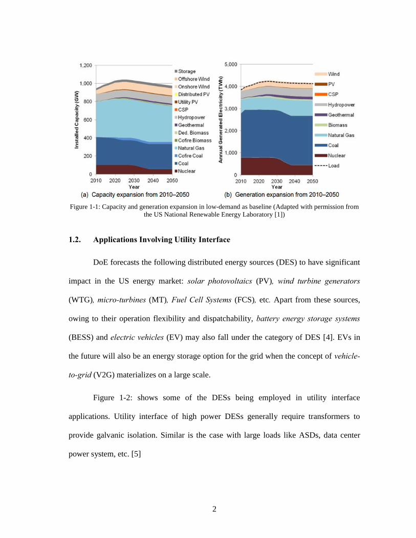
The world has seen a steep rise in the usage of renewable energy resources,
driven by issues such as global warming, depletion of non-renewable energy sources,
etc. The United States’ Department of Energy (DoE) predicts that as a proportion of total
electricity supply, renewable energy sources will contribute almost 20 % in the year
2050 compared to 12 % in 2010 (see Figure 1-1 from NREL report [1]). In order to
utilize these vast energy resources, energy has to be converted from one form to another
and interfaced to the electric grid. This has significantly increased the prospects of
power electronics in the energy sector [2].
Power converters process the power generated from renewable energy sources
such as wind turbines, solar photovoltaics (PV), etc., and convert them to the voltage and
frequency levels suitable for the utility grid. Not only in power generation, but power
electronic converters are also used to interface different high power electro-mechanical
loads to the utility grid, such as adjustable speed drives (ASDs), electric vehicle (EV)
battery, uninterruptable power supply (UPS), etc. Recently, governments have also
started coming up with certain energy storage mandates, targeting the use of battery and
other energy storage media to offset the demand-supply gap in the electric grid or to act
as buffer for the intermittent and unpredictable renewable energy sources [3]. The
objective of future power conversion will be processing maximum power with the
highest efficiency and reliability, at the smallest footprint and cost.
2
Figure 1-1: Capacity and generation expansion in low-demand as baseline (Adapted with permission from
the US National Renewable Energy Laboratory [1])
1.2. Applications Involving Utility Interface
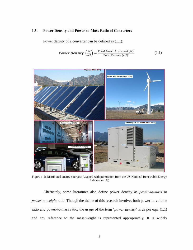
DoE forecasts the following distributed energy sources (DES) to have significant
impact in the US energy market: solar photovoltaics (PV), wind turbine generators
(WTG), micro-turbines (MT), Fuel Cell Systems (FCS), etc. Apart from these sources,
owing to their operation flexibility and dispatchability, battery energy storage systems
(BESS) and electric vehicles (EV) may also fall under the category of DES [4]. EVs in
the future will also be an energy storage option for the grid when the concept of vehicle-
to-grid (V2G) materializes on a large scale.
Figure 1-2: shows some of the DESs being employed in utility interface
applications. Utility interface of high power DESs generally require transformers to
provide galvanic isolation. Similar is the case with large loads like ASDs, data center
power system, etc. [5]
3
(1.1)
1.3. Power Density and Power-to-Mass Ratio of Converters
Power density of a converter can be defined as (1.1):
𝑃𝑜𝑤𝑒𝑟 𝐷𝑒𝑛𝑠𝑖𝑡𝑦 (𝑊
𝑚3) =𝑇𝑜𝑡𝑎𝑙 𝑃𝑜𝑤𝑒𝑟 𝑃𝑟𝑜𝑐𝑒𝑠𝑠𝑒𝑑 (𝑊)
𝑇𝑜𝑡𝑎𝑙 𝑉𝑜𝑙𝑢𝑚𝑒 (𝑚3)
Figure 1-2: Distributed energy sources (Adapted with permission from the US National Renewable Energy
Laboratory [4])
Alternately, some literatures also define power density as power-to-mass or
power-to weight ratio. Though the theme of this research involves both power-to-volume
ratio and power-to-mass ratio, the usage of the term ‘power density’ is as per eqn. (1.1)
and any reference to the mass/weight is represented appropriately. It is widely
4
considered that in order to scale up large power systems such as wind turbines, electric
locomotives, etc., power density has to be increased. DoE has set a target to reduce the
production cost of electric tractions by 50% and increase the power density by 20% by
2020. Advantages of achieving higher power density are: reduced weight/footprint,
reduced fuel consumed during transportation, reduced cost, simpler
installation/maintenance, etc.
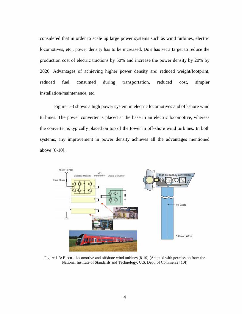
Figure 1-3 shows a high power system in electric locomotives and off-shore wind
turbines. The power converter is placed at the base in an electric locomotive, whereas
the converter is typically placed on top of the tower in off-shore wind turbines. In both
systems, any improvement in power density achieves all the advantages mentioned
above [6-10].
Figure 1-3: Electric locomotive and offshore wind turbines [8-10] (Adapted with permission from the
National Institute of Standards and Technology, U.S. Dept. of Commerce [10])

5
1.3.1. Components Affecting Power Density
A typical power conversion scheme for utility integration has the following
major components: power semiconductor devices (IGBTs, MOSFETs, etc.), filter
passive components (inductors, capacitors, etc.), DC-link capacitor, heat sink, power
transformer. Figure 1-4 shows the comparison of space occupied by different
components in a non-isolated DC-AC inverter (rated 10 kW) [11]. The 2-Level Voltage
Source Inverter (2LVSI) along with boost converter (BC) at 8 kHz occupies almost 4.0 L
(1 L = 1 dm3), with the inductor occupying around 2.5 L, the DC capacitor, devices and
heat sink occupying 0.5 L each.
Figure 1-4: Volume of components in a 10 kW DC-AC converter (© 2013 IEEE [11] – Adapted with
permission from the IEEE)
If galvanic isolation has to be added to this system, a reasonable volume estimate
of a 10 kVA transformer is around 20 L, which is greater than 80% of the entire system
volume. From this, it can be stated that the magnetic components such as transformer
and inductor, typically affect the power density of a power conversion scheme. Not only
the volume, but the magnetic components also affect the weight of the converter almost
6
to the same extent. Magnetic components are followed by DC-link capacitors and heat
sinks in terms of size. Any reduction in the size of these components will drastically
improve the system power density, especially in systems where it is either mandated or
desired to employ power transformers for isolation.
1.3.2. Methods to Improve Converter Power Density
One of best known methods to improve the power density of converters is to
increase the frequency of the transformer or inductor core [12-14]. At a higher
frequency, a transformer core can carry the same amount of flux lines at a smaller area
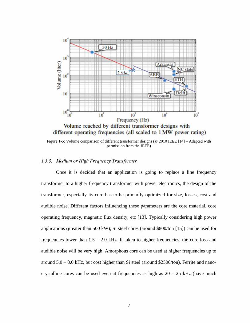
(assuming same flux density). From Figure 1-5 [14], it can be noticed that the volume of
a 1 MVA silicon (Si) steel core transformer can be reduced from 2000 L to 200 L if the
core frequency is increased from 50 Hz to 1000 Hz. This transformation in the frequency
can be implemented using power electronics. Though it is possible to increase the
frequency and reduce the volume/weight, this may lead to higher losses and audible
noises if the magnetic flux density is not chosen appropriately. If a better core such as
amorphous silicon (Si) or nano-crystalline Si is employed instead of conventional Si
steel core, this further increases the cost. Power electronics further adds to cost and
power losses, also affects the system reliability. This research does not focus on the
reliability aspect, though reliability can be a major factor for commercialization.
7
Figure 1-5: Volume comparison of different transformer designs (© 2010 IEEE [14] – Adapted with
permission from the IEEE)
1.3.3. Medium or High Frequency Transformer
Once it is decided that an application is going to replace a line frequency
transformer to a higher frequency transformer with power electronics, the design of the
transformer, especially its core has to be primarily optimized for size, losses, cost and
audible noise. Different factors influencing these parameters are the core material, core
operating frequency, magnetic flux density, etc [13]. Typically considering high power
applications (greater than 500 kW), Si steel cores (around $800/ton [15]) can be used for
frequencies lower than 1.5 – 2.0 kHz. If taken to higher frequencies, the core loss and
audible noise will be very high. Amorphous core can be used at higher frequencies up to
around 5.0 – 8.0 kHz, but cost higher than Si steel (around $2500/ton). Ferrite and nano-
crystalline cores can be used even at frequencies as high as 20 – 25 kHz (have much

8
lower core losses), but the materials are very expensive (more than $12000/ton).
Moreover if desired to operate at very high frequencies, the skin effect and corona effect
will be significant and it might become necessary to construct the transformer larger,
losing out a little on the size advantage. Also, the power converter switching loss will be
much higher even with soft-switching techniques. Overall, the transformer has to be
designed according to the application. Table 1-1 shows an example design of a 60 Hz
and a 1000 Hz transformer for 142 kVA power (Si steel core). It can be seen that the
1000 Hz transformer is almost 25% of the volume and much lower in cost compared to
60 Hz transformer. This may offset the power electronics cost.
Table 1-1: An example design comparison of a 60 Hz transformer and a 1000 Hz transformer
1.4. Power Converter Modelling and Implementation
This section explains certain basic concepts of deriving the switching function of
a converter, and later selecting the converter to implement the switching function. Once
the specifications of the input and output of a converter are given, the switching function

9
can be defined as the ratio of output voltage to the input voltage. Figure 1-6 shows the
switching function for a power converter when the input is DC and the output desired is
a high frequency square wave. The frequency spectrum (FFT) of output voltage shown
in Figure 1-6 confirms the equations.
Figure 1-6: Square wave switching function for DC input
Figure 1-7 shows the switching function and output voltage of a power converter
when the input is low frequency sinusoidal AC and the output desired is of high
frequency AC. The frequency spectrum (FFT) of output voltage in such a case is also
shown in Figure 1-7. Unlike the earlier situation, the output here is a multiplication of
the input low frequency sine wave and higher frequency square wave switching function.
From the equations, it can be seen that the output voltage equation can be obtained by
simply multiplying the input with the switching function. Assuming ωs is the input
frequency and ωsq is the square wave frequency, the output voltage has fundamental
frequency as ωsq ± ωs as verified by the FFT in Figure 1-7.
10
Figure 1-7: High frequency square wave switching function for low frequency sinusoidal input
From Figure 1-7, it can be seen that a square wave modulation creates many
frequency tones at 3ωsq ± ωs, 5ωsq ± ωs, etc. on the output, due to the higher order terms
present in the Fourier series expansion of a square wave (switching function). If only the
fundamental tone(s) is (are) required, a physical filter can be placed at the output.
Otherwise, the converter modulation can be selected as a higher frequency sine wave.
Instead of a medium or high frequency square wave, it is possible to modulate
the converter with a sine PWM switching function, as shown in Figure 1-8. It can be
seen from Figure 1-8 that when an input sinusoidal voltage of frequency ωs is operated
upon by a sine PWM of fundamental frequency ωmf, the output once filtered is a voltage
waveform of frequencies ωmf ± ωs.

11
Figure 1-8: High frequency sine PWM switching function for low frequency sinusoidal input
However in power electronics, the switching states are discrete and it is difficult
to do amplitude modulation. Instead, pulse-width modulation (PWM) methods can be
used where a sine wave can be interfaced with a higher frequency triangle in such a way
that the switching function has a desired fundamental frequency and the next frequency
is close to the frequency of the interfacing triangle (PWM frequency). Such a scheme
can reduce the filter size since the PWM frequency can be chosen to be much higher,
only limited by the device losses. Figure 1-9 shows two of the major methods by which
this can be achieved – bipolar PWM and unipolar PWM.
Using PWM scheme, any desired switching function can be implemented; it can
even be a sum or product of many different switching functions. There are alternate
switching methods too, such as programmed PWM, Space Vector (SV) PWM, etc.
12
Figure 1-9: Sinusoidal PWM switching function – bipolar and unipolar versions
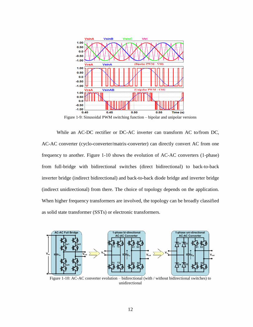
While an AC-DC rectifier or DC-AC inverter can transform AC to/from DC,
AC-AC converter (cyclo-converter/matrix-converter) can directly convert AC from one
frequency to another. Figure 1-10 shows the evolution of AC-AC converters (1-phase)
from full-bridge with bidirectional switches (direct bidirectional) to back-to-back
inverter bridge (indirect bidirectional) and back-to-back diode bridge and inverter bridge
(indirect unidirectional) from there. The choice of topology depends on the application.
When higher frequency transformers are involved, the topology can be broadly classified
as solid state transformer (SSTs) or electronic transformers.
Figure 1-10: AC-AC converter evolution – bidirectional (with / without bidirectional switches) to
unidirectional

13
1.5. Research Objective
From the earlier sub-sections, it is evident that the power electronics industry is
moving towards higher efficiency at lower cost and smaller footprint. In response to this
growing demand for smaller and less expensive energy conversion, this dissertation aims
to propose, design, analyze and test isolated power converter topologies that improve the
power density of certain utility interface applications, such as wind turbine generators
(WTGs), adjustable speed drives (ASDs), etc., over the conventional topologies. All the
proposed topologies employ unidirectional or bidirectional AC-AC converters and also
use medium frequency (MF) or high frequency (HF) transformers to achieve higher
power density. AC-AC converters avoid DC electrolytic capacitors due to pulsating
(weak) DC bus instead of a stiff one. The major concepts discussed earlier in this section
are used at multiple locations throughout this dissertation.
A conventional WTG system uses back-to-back inverters that convert low
frequency AC to the line frequency AC, which is then interfaced to the utility grid via a
bulky line frequency transformer. In case of a large ASD system, a 12-pulse or 18-pulse
diode rectifier configuration is usually used, which also employ line frequency
transformers in star-delta configuration. When analyzed in depth, the largest components
present in these conventional topologies are mostly the line frequency transformers and
the filter inductors. They are also usually the most expensive components too. The theme
of this dissertation revolves around identifying and formulating alternative strategies that
replace the bulky line frequency transformers with a combination of AC-AC converters
and higher frequency transformers. The sole purpose of the AC-AC converters is to

14
modulate the line frequency voltage to higher frequency AC suitable to interface with a
MF or HF transformer. In order to interface the system with a medium voltage (MV)
utility grid, multi-level AC-AC converters can be used. One such multi-level approach
has also been studied and experimented in this dissertation. Wherever possible, simple
open loop control strategies are employed. Even where closed loop control is required,
conventional PI control is used most of the time, which makes the proposed approaches
attractive to the industry.
Once it is decided that a higher frequency transformer is desired for an
application, there are two main choices – (a) use silicon steel, powdered iron or
amorphous silicon core based MF transformer or (b) use ferrite or nano-crystalline core
based HF transformer. A MF transformer made with silicon steel or amorphous core
operating at or around 1 kHz can be as small as 25 % of a 60 Hz transformer, while a HF
transformer using ferrite core operating at or above 10 kHz can be constructed to be
much smaller. But factors such as higher corona loss, higher converter switching loss,
higher material cost, etc. restrict the advantages of size reduction in HF transformers.
This dissertation hence concentrates more on MF transformer based approaches, but
even higher frequency transformer based approaches have been studied in brief.
Moreover most of the proposed topologies can be extended to higher frequencies.
After designing and analyzing the proposed topologies, simulations have been
done for each concept. Further, experimental results on scaled down laboratory
prototypes validate the functionality of the proposed topologies. Since hardware
demonstrations could not be carried out on megawatt scale due to restrictions in the set-
15
up, 2-D finite element analyses are done using ANSYS Maxwell software, using which
it is possible to do comparisons on loss, size and saturation effects of transformers under
different core materials for the proposed techniques. These studies conclude the research
performed through this dissertation.
1.6. Outline of Dissertation
This dissertation is organized into seven sections. Section 1 introduces the main
utility interface applications and the concepts of power density in power converters. The
size benefits of using a MF or HF transformer over a line frequency transformer are
explained in detail. Mathematical modeling of power converters at various modulation
schemes is elucidated and the section concludes by describing the research objective.
Since the organization of the dissertation is into different applications, literature review
is covered at the beginning of each major section.
Section 2 proposes an isolated 3-phase AC-DC converter that employs a MF or
HF transformer and avoids DC electrolytic capacitors on the utility side power converter.
The proposed topology is then compared with a conventional scheme in terms of size
and efficiency. The control strategy is also explained in detail in this section and the
concept is validated through simulation and experiments. Section 3 proposes a simple
multi-pulse diode rectifier concept using MF or HF transformers that replace bulky line
frequency transformers in a conventional multi-pulse rectifier. Theory, analysis,
simulation and experiments are performed for a 12-pulse rectifier configuration, but a
generic scheme to extend this strategy towards 18-pulse or 24-pulse rectifier is also
shown in this section. Section 3 also proposes an alternate isolated AC-DC rectifier
16
suitable for ASDs, WTGs, etc., especially for medium voltage (MV) applications. Here,
the utility AC is converted to MF AC, which is then fed to three 1-phase MF
transformers. The secondary side of the transformers are connected in star or delta
configuration and then fed to 3-phase diode rectifiers as in a 6-pulse rectifier. Detailed
analysis, simulation and experimental results are presented in this section.
Section 4 extends some of the concepts proposed in sections 2 and 3; and applies
them to develop topologies for wind turbine generator (WTG) – medium voltage DC
(MVDC) interconnection that are suitable for offshore farms and long-distance
transmission line. The section starts with the introduction to offshore wind farms and
some of the WTG – MVDC converters already proposed in the literature. Then the
proposed topologies are explained, followed by detailed analysis and simulation results.
Section 5 starts with the introduction of battery energy storage systems (BESS) in
modern day grid and the benefits of employing megawatt scale BESS on the stability of
the power grid. Then a MF transformer based approach is proposed for interfacing a
large scale BESS system to the utility grid. As an extension, a 3-port scheme for
interfacing a WTG system along with a BESS system is introduced in this section.
Detailed simulation and experimental results are also shown.
Section 6 discusses about modeling the MF or HF transformer using ANSYS
Maxwell software. The approaches proposed in the earlier sections are evaluated for
their transformer design under the criteria of size and losses. Comparison in terms of size
and losses in the MF or HF transformers (using electrical steel, amorphous and ferrite
core materials) with respect to the line frequency transformer are also shown. The

17
section concludes by explaining about the variation of overall size and efficiency of the
power converter system for different transformer core materials.
Section 7 provides a summary of the research work reported in this dissertation
and concludes with recommendations for future research topics in this area.

18
2. HIGH POWER AC-DC CONVERTER WITH BOOST PFC
2.1. Isolated AC-DC Converters
AC-DC converters have become a commodity in consumer electronics and due to
stringent safety standards; many of them either have mandatory specifications or
requirements on galvanic isolation. AC-DC converters using high frequency (HF) or
medium frequency (MF) transformers are popularly used in electric vehicle (EV)
charging, adjustable speed drives (ASDs), server power supplies, 3-phase battery
chargers, etc. [16-18]
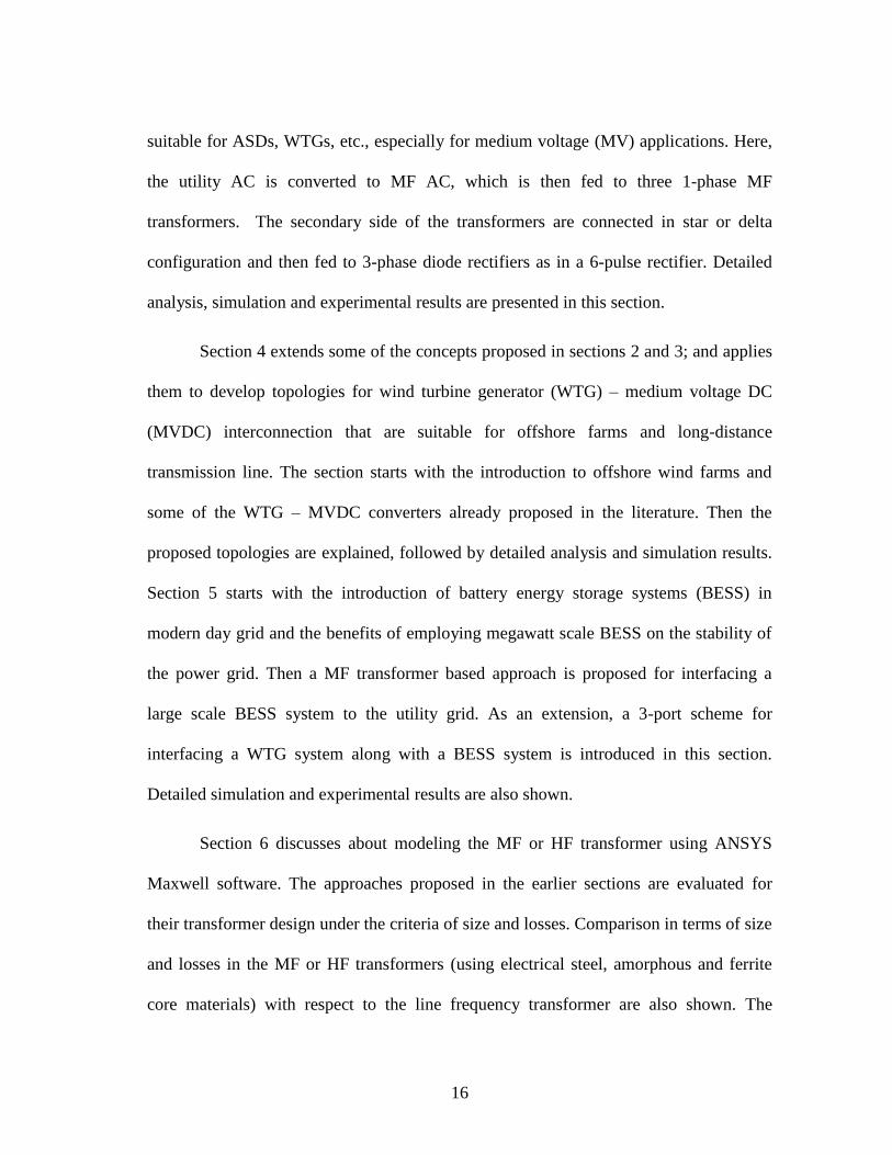
One of the very conventional topologies involves a simple 3-phase diode rectifier
front-end, a stiff DC-link follower by an isolated DC-DC converter, as shown in Figure
2-1. But this has high input current harmonics, due to the rectifier operation, which
increases filter requirement. A popular topology for a 1-phase high power isolated AC-
DC converter used extensively is a boost power factor correction (PFC) stage followed
by a DC-DC converter stage [16, 19, 20]. Many 3-phase isolated AC-DC converters also
employ a similar scheme by having the three phases connected in parallel on the output
DC side, as in Figure 2-2 [21]. As seen in Figure 2-2, the boost PFC stage operation
makes the inductor current in phase and shape as the diode rectified pulsating DC
voltage, thereby making the utility power factor close to unity. In effect, the PFC stage
emulates an ‘active resistor’ to the utility grid. Since the H-bridge of the isolated DC-DC
converter stage requires a fixed DC, the boost PFC stage output DC-link capacitors have
to be large (to suppress the 2nd harmonic ripple). Moreover, the square wave shape of
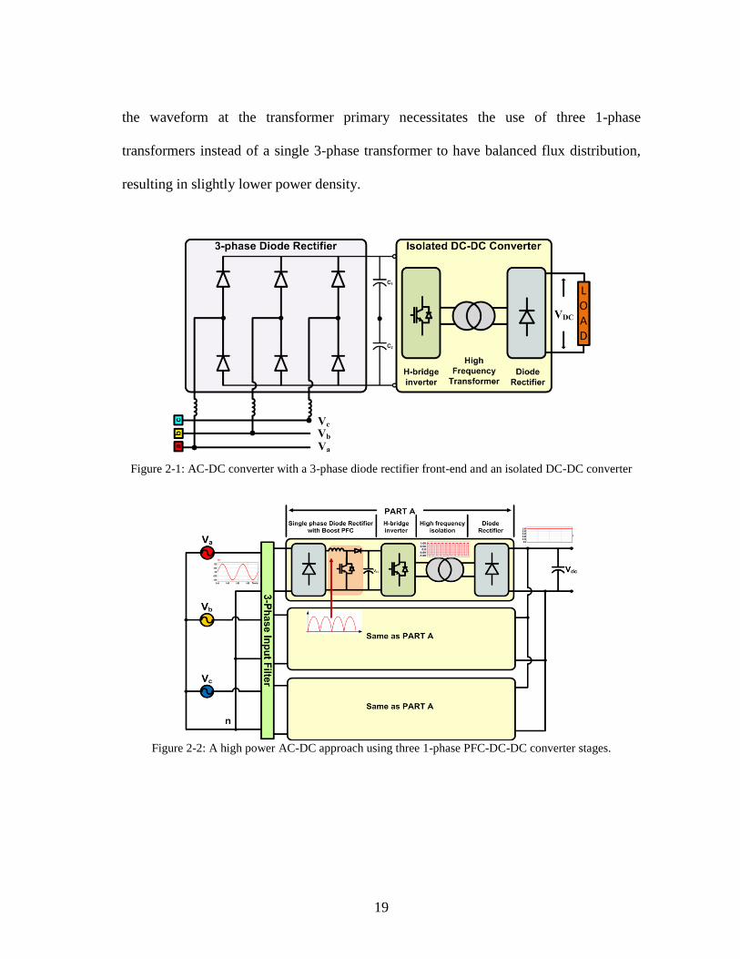
19
the waveform at the transformer primary necessitates the use of three 1-phase
transformers instead of a single 3-phase transformer to have balanced flux distribution,
resulting in slightly lower power density.
Figure 2-1: AC-DC converter with a 3-phase diode rectifier front-end and an isolated DC-DC converter
Figure 2-2: A high power AC-DC approach using three 1-phase PFC-DC-DC converter stages.

20
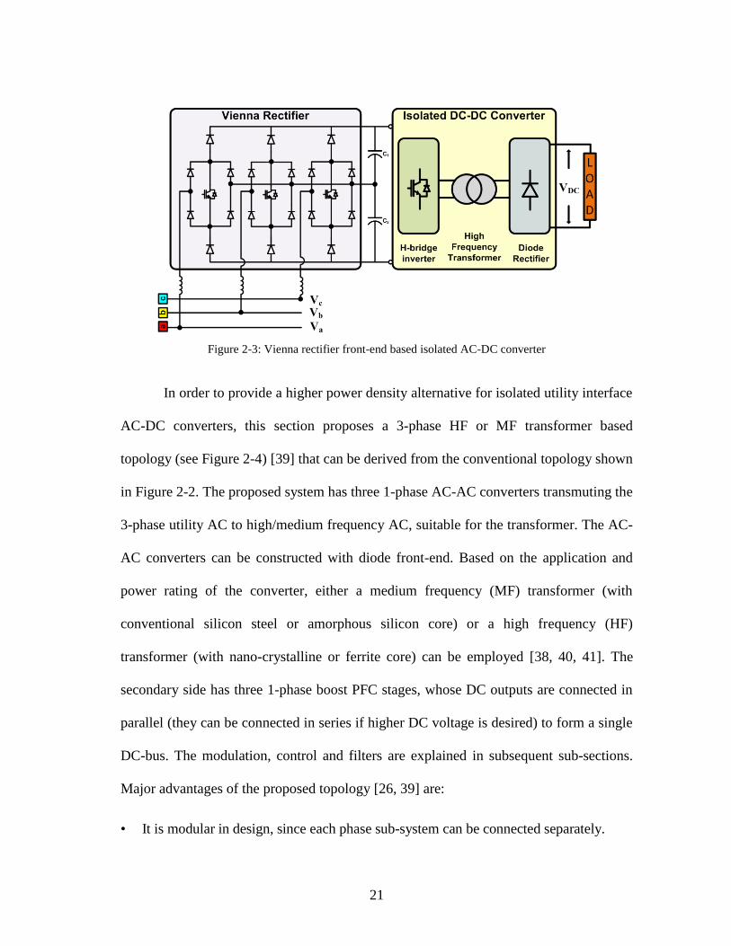
Several other AC-DC converters have been proposed in the literature [22-28].
Some of the popular configurations, namely Swiss rectifier, Vienna rectifier, Y-rectifier,
etc, have been summarized in [27, 29, 30].Many of these configurations are suitable for
non-isolated AC-DC converters or require a separate DC-DC converter for isolation.
Some may also require additional circuitry to achieve unity power factor (UPF) at the
utility side. Figure 2-3 shows a Vienna rectifier-front-end based isolated AC-DC
converter, which is an improvement over the system shown in Figure 2-1, enabling
better input current quality. But this topology has seven power semiconductor devices
for each leg, contributing to higher conduction losses.
A single phase AC-DC power converter is proposed in [31], that uses flyback
transformer and a resonant active-clamp circuit. Different PFC topologies in flyback as
well as bridged configurations in interleaved structure have been proposed in [32-35].
Some approaches such as [31, 36, 37] employ soft-switching for obtaining higher
efficiencies even at higher frequencies for rectifier applications. Since AC-DC
conversion is a very important segment in systems involving distributed energy sources,
several unidirectional and bidirectional topologies have been proposed for such
applications that use either line frequency or higher frequency transformers for isolation
[21, 22, 38]. Many of these topologies either use large electrolytic capacitors or employ
complicated control strategies.
21
Figure 2-3: Vienna rectifier front-end based isolated AC-DC converter
In order to provide a higher power density alternative for isolated utility interface
AC-DC converters, this section proposes a 3-phase HF or MF transformer based
topology (see Figure 2-4) [39] that can be derived from the conventional topology shown
in Figure 2-2. The proposed system has three 1-phase AC-AC converters transmuting the
3-phase utility AC to high/medium frequency AC, suitable for the transformer. The AC-
AC converters can be constructed with diode front-end. Based on the application and
power rating of the converter, either a medium frequency (MF) transformer (with
conventional silicon steel or amorphous silicon core) or a high frequency (HF)
transformer (with nano-crystalline or ferrite core) can be employed [38, 40, 41]. The
secondary side has three 1-phase boost PFC stages, whose DC outputs are connected in
parallel (they can be connected in series if higher DC voltage is desired) to form a single
DC-bus. The modulation, control and filters are explained in subsequent sub-sections.
Major advantages of the proposed topology [26, 39] are:
• It is modular in design, since each phase sub-system can be connected separately.
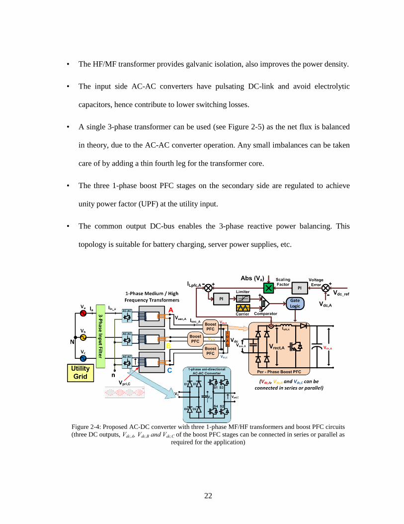
22
• The HF/MF transformer provides galvanic isolation, also improves the power density.
• The input side AC-AC converters have pulsating DC-link and avoid electrolytic
capacitors, hence contribute to lower switching losses.
• A single 3-phase transformer can be used (see Figure 2-5) as the net flux is balanced
in theory, due to the AC-AC converter operation. Any small imbalances can be taken
care of by adding a thin fourth leg for the transformer core.
• The three 1-phase boost PFC stages on the secondary side are regulated to achieve
unity power factor (UPF) at the utility input.
• The common output DC-bus enables the 3-phase reactive power balancing. This
topology is suitable for battery charging, server power supplies, etc.
Figure 2-4: Proposed AC-DC converter with three 1-phase MF/HF transformers and boost PFC circuits
(three DC outputs, Vdc,A, Vdc,B and Vdc,C of the boost PFC stages can be connected in series or parallel as
required for the application)

23
2.2. Proposed 3-phase Isolated AC-DC Converter Topology
Figure 2-4 illustrates the proposed AC-DC converter topology, with three 1-
phase MF transformers and a single 3-phase transformer, respectively. While a single 3-
phase transformer can be a cheaper option compared to three 1-phase transformer bank,
operating at higher frequencies can cause flux imbalance. So a dummy fourth leg can be
included in the design to avoid saturation due to unintended low frequency components
or resonances as in Figure 2-5. The remaining of this section explains the topology
considering separate 1-phase transformers. The design of the converter can be broadly
divided into the following main sub-sections: AC-AC converter, HF or MF transformer,
1-phase boost PFCs, modulation schemes and control strategy, which are explained in
detail further in this section.
2.2.1. AC-AC Converter
There are three 1-phase unidirectional AC-AC converters in the proposed
topology. The front-end can be constructed using AC-AC full-bridges with bidirectional
switches (see Figure 1-10) or using a 1-phase diode bridge and a 1-phase inverter H-
bridge (with IGBTs or FETs) connected bact-to-back (since power transfer is
unidirectional) with de-coupling capacitors as shown in Figure 2-4 [26, 39]. In order to
interface to a 208V, fs = 60Hz 3-phase utility grid, 450V or lower rated standard IGBTs
or MOSFETs will be sufficient. The AC-AC converter in each phase is modulated with a
high frequency (HF) or medium frequency (MF) square wave (fsq = ωsq/2π). The phase
A utility voltage- Va, the AC-AC converter switching function- Sacac, and the transformer
primary voltage of phase A- Vpri,A, can be given by (2.1), (2.2) and (2.3):
(2.1)
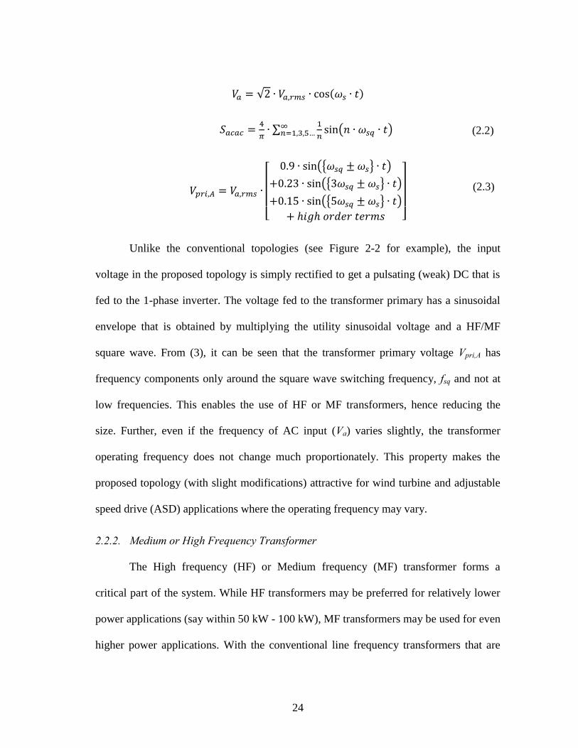
24
𝑉𝑎 = √2 ∙ 𝑉𝑎,𝑟𝑚𝑠 ∙ cos(𝜔𝑠 ∙ 𝑡)
𝑆𝑎𝑐𝑎𝑐 =4
𝜋∙ ∑
1
𝑛
∞𝑛=1,3,5… sin(𝑛 ∙ 𝜔𝑠𝑞 ∙ 𝑡)
𝑉𝑝𝑟𝑖,𝐴 = 𝑉𝑎,𝑟𝑚𝑠 ∙
[
0.9 ∙ sin({𝜔𝑠𝑞 ± 𝜔𝑠} ∙ 𝑡)
+0.23 ∙ sin({3𝜔𝑠𝑞 ± 𝜔𝑠} ∙ 𝑡)
+0.15 ∙ sin({5𝜔𝑠𝑞 ± 𝜔𝑠} ∙ 𝑡)
+ ℎ𝑖𝑔ℎ 𝑜𝑟𝑑𝑒𝑟 𝑡𝑒𝑟𝑚𝑠 ]
Unlike the conventional topologies (see Figure 2-2 for example), the input
voltage in the proposed topology is simply rectified to get a pulsating (weak) DC that is
fed to the 1-phase inverter. The voltage fed to the transformer primary has a sinusoidal
envelope that is obtained by multiplying the utility sinusoidal voltage and a HF/MF
square wave. From (3), it can be seen that the transformer primary voltage Vpri,A has
frequency components only around the square wave switching frequency, fsq and not at
low frequencies. This enables the use of HF or MF transformers, hence reducing the
size. Further, even if the frequency of AC input (Va) varies slightly, the transformer
operating frequency does not change much proportionately. This property makes the
proposed topology (with slight modifications) attractive for wind turbine and adjustable
speed drive (ASD) applications where the operating frequency may vary.
2.2.2. Medium or High Frequency Transformer
The High frequency (HF) or Medium frequency (MF) transformer forms a
critical part of the system. While HF transformers may be preferred for relatively lower
power applications (say within 50 kW - 100 kW), MF transformers may be used for even
higher power applications. With the conventional line frequency transformers that are
(2.2)
(2.3)

25
constructed using silicon steel core (magnetic flux density of around 1.2 T to 1.5 T), the
core loss is not too large as the line frequency is low. But if it is desired to reduce the
size of the system by increasing the silicon steel transformer core frequency, the core
losses also increase. To an extent, this increase in losses can be compensated by
reducing the magnetic flux density to around 0.3 T to 0.6 T; this also helps in reducing
the possibilities of core getting saturated. This strategy can work until certain ‘medium
frequencies’ around 1 kHz to 1.5 kHz, at a lower transformer cost since the silicon steel
core material used is much lesser (a 1000 Hz, 0.4 T MF transformer with silicon steel
core can be approximately one-fourth the size of a 60 Hz, 1.5 T line frequency
transformer for the same core losses). These aspects are explained in much more detail
in section 6.
Beyond this MF range, it becomes necessary to employ amorphous silicon core
or powdered iron core because the audible noise increases significantly and it becomes
difficult to optimize the system for losses. But this adds to the cost of the transformer
and the audible noise issues may not be solved completely. If much higher transformer
operating frequencies are desired to further reduce the size, ferrite or nano-crystalline
cores would be more suitable. For high power applications beyond a few hundred
kilowatts, usage of ferrite core transformers get complicated due to high corona effects
and possible flux leakage. The power converter losses also increase significantly. In such
cases, it is more appropriate to design and use MF transformers.
If ‘β’ is the boost PFC gain (~ 1.5 to 2.0) and Vdc is the required DC output
voltage, the required transformer turns-ratio, N can be calculated as per (2.4). For a
26
208VLL utility input, 200Vdc DC voltage and for a β value of 1.5, the transformer turns
ratio is approximately n2:n1 = 6:5.
𝑁 =𝑛2
𝑛1= (
𝜋
2√2∙𝛽) ∙ (
𝑉𝐷𝐶
𝑉𝑎(𝑟𝑚𝑠))
As discussed earlier, since the modulation is in such a way that the AC-AC
converter output voltages add to zero, the net magnetic flux will always be balanced
ideally even if a single 3-phase MF transformer is used instead of three 1-phase
transformers. But in practice, there will be slight imbalances caused by converter
operation, resonances, etc. To compensate for these imbalances, a thin fourth leg can be
added to the 3-phase core in order to avoid saturation, as shown in Figure 2-5.
Figure 2-5: Proposed converter with a single 3-phase transformer instead of three 1-phase transformers
(2.4)

27
2.2.3. 1-phase Boost PFC Stage
The transformer secondary voltage is a ‘flipped sine wave’ (product of line
frequency sine and HF/MF square wave as shown in Figure 2-4, slightly smoothened
due to the filtering action of the transformer leakage inductance. The diode rectifiers of
the boost PFC stage convert this flipped sine wave into full-wave rectified (twice-the-
line-frequency) waveform. It should be noted that even though the transformer
frequency is HF or MF, the diode rectifiers switch at that frequency and the rectified
voltages look similar to the rectified voltage waveforms of the weak DC-link on the
primary side. After this, the remaining boost converter section operates like the one in a
conventional boost PFC, making the inductor current in phase and shape as the rectified
voltage. Hence the design of this topology is straight forward.
The switching devices in the boost PFC stage have to be rated at least at the peak
output DC voltage. If the output DC voltage has to be regulated at 200 V, then the boost
PFC switches have to be rated at 350V. It is important to note that the output voltage, Vdc
must be equal to or greater than the peak rectified voltage. The design equations for the
PFC inductors LPFC and the effective output capacitors Cdc can be given by (2.5) and
(2.6). As a design rule considered, the inductors must make the boost PFC operate at
continuous conduction beyond 20 % load, thus the current ripple must be less than 20 %
of load current at the peak rectified voltage. Assuming the peak voltage across the
inductor is Vdc, if ‘D’ is the duty cycle, ‘fsw’ is the switching frequency and ip-p is the
ripple current peak-to-peak (equal to 20% of load current),

28
𝐿𝑃𝐹𝐶 = (𝐷∙𝑉𝐷𝐶
𝑓𝑠𝑤∙𝑖𝑝−𝑝)
Since the boost PFC outputs are connected in parallel, the 2nd
harmonic ripples of
the three phases get cancelled and hence the capacitor only needs to be designed for the
switching frequency of the boost PFC stage. Otherwise, the capacitor design is
completely dependent upon the subsequent stage after the PFC. Assuming the PWM
signals to the PFCs for the three phases are phase shifted by 120o, the ripple voltage
across the capacitor will be at thrice the switching frequency. As a thumb rule, the
capacitor can be designed as:
𝐶𝐷𝐶 = (𝑖𝑝−𝑝
2∙𝜋∙𝑓𝑠𝑤∙𝑣𝑝−𝑝)
where vp-p is the ripple voltage pk-pk allowed at the output capacitor. If ip-p = 4 A, fsw =
3.6 kHz, Vdc = 200 V, D = 0.2 and vp-p = 10 V, then LPFC ~= 2.5 mH and CDC ~= 25 uF.
A 330 uF capacitor is chosen to support the subsequent stage.
2.2.4. Control Strategy
Figure 2-6: Single-phase equivalent circuit with control system for the proposed topology (Figure 2-4)
(2.5)
(2.6)

29
It should be noted that there is no closed loop control involved on the primary
side of the proposed system since the AC-AC converters are operated using simple
HF/MF square wave modulation. The utility input current and output DC voltage are
regulated through the control of the boost PFC stage. The control objective is similar to
that of the boost PFC stage in a conventional AC-DC converter (Figure 2-2), which is to
emulate an active resistor that makes the input current’s shape and phase follow that of
the input voltage. Here the boost PFC stages try to make the transformer currents’ shape
and phase follow that of the primary voltages, Vpri,ph. Figure 2-6 depicts the control
strategy employed in proposed topology. Depending upon the load power, the magnitude
of the PFC inductor current, ILpfc,A, is varied by adjusting the scaling factor that is
generated from the output DC voltage (Vdc,A) regulation; keeping the shape same as that
of the rectified voltage, Vrect,A. Since Vrect,A is the same as the rectified voltage of a
conventional boost PFC system, the design and control here are similar to a conventional
boost PFC.
The inner current control loop must be faster than the outer voltage loop. For
tuning the control parameters, methods such as Ziegler Nichols can be used. When the
DC outputs of the boost PFC stages corresponding to the three phases are connected
either in series or parallel, the second harmonic power gets cancelled and hence the DC
capacitor need not be very large. In the topology shown in Figure 2-2, the DC capacitors
at the output of the boost PFC stages on the transformer primary side need to suppress
the second harmonic current ripple will be large. This is a notable advantage of the
proposed topology. Other advantages are reduction in size and switching losses, which

30
are explained in the next section. The utility currents will have small twice the MF
components due to transformer current transients; these are filtered using LC filter [27].
2.3. Size and Loss Comparison
The major difference between the conventional AC-DC topology in Figure 2-2
and the proposed system in Figure 2-4 is that there is no stiff DC link in the primary side
of the transformer in the proposed topology. An advantage having a weak DC-link on
the primary side, apart from avoiding large electrolytic capacitors, is that since the AC-
AC converter is switched with identical square wave in all the three phases, the net flux
in the transformer will be balanced even if a single 3-phase transformer is used as shown
in Figure 2-5. In the topology in Figure 2-2, due to a stiff DC-link on the primary side,
either three 1-phase transformers need to be used or resonant power conversion strategy
(like LC or LLC resonant soft-switching) needs to be used. This increases the system
size. Moreover, if same devices are used in both cases, the voltage stress on the devices
is lower here than in the conventional topology.
Another advantage of having a pulsating DC link on the primary side is that the
switching losses are lower. Since the switching loss is proportional to the product of the
DC-link voltage and current, if the average value of DC-link voltage is lower, the
switching losses are lower (for the same rms current). Hence the switching losses with
pulsating DC-link may become (2/π) times (~35% reduction) for the H-bridge.
A disadvantage of the proposed topology is that due to the presence of diode
rectifiers on both the AC-AC converter front end and boost PFC front-end, supplying

31
non-unity power factor on the utility side can result in increased harmonic distortion.
Also, the diode rectifiers on the boost PFC stage need to operate at HF/MF. But since
most utility interface systems require unity power factor at the input and due to the
increased availability of fast-switching rectifiers, these disadvantages do not possess
significant challenges, at least for MF transformer based applications. Size and loss
analysis for the proposed MF/HF transformer based topologies will be explained in
detail in section 6.
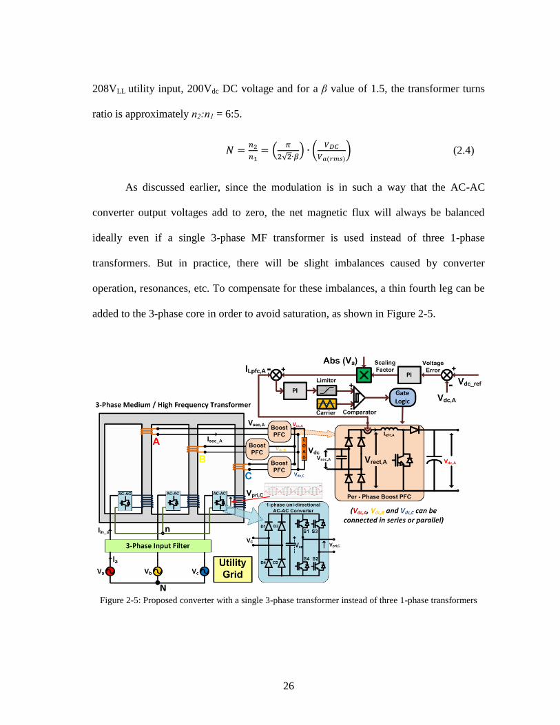
2.4. Simulation and Experimental Results
Table 2-1: Simulation parameters and values
Parameters Values
Input AC 208 VLL, 60 Hz, 3-phase
Output DC Load 200 V, 4 kW
Transformer Core Silicon Steel, 600 Hz (MF)
Transformer Leakage 0.05 p.u. per winding
Input AC filter capacitance 0.1 mF
DC side filter capacitance 330 uF
Boost PFC Switching Frequency 3.6 kHz
The topology in Figure 2-4 was simulated using PSIM. The specifications of the
system are provided in Table 2-1. Figure 2-7 and Figure 2-8 show the important
waveforms obtained during the simulation of the proposed topology using a resistive
load of 4 kW. It can be seen from Figure 2-7 (a) that the utility input voltage and current
are in phase and the current has very low harmonics. Figure 2-7 (b) shows the primary
side rectified voltage and current at the weak DC-link of the AC-AC converter. There
32
are some resonances seen in the current, which is due to the input filter inductance and
coupling capacitor. Figure 2-7 (c) shows the MF/HF transformer primary voltage and
current, which are again in phase and similar in shape.
Figure 2-7: Simulation waveforms of the transformer primary side of the proposed topology - (a) Utility
input phase-A voltage and current (scale increased for better resolution of current); (b) Pulsating DC-link
voltage and current; and (c) Transformer primary phase-A voltage and current
Figure 2-8 shows the simulation waveforms on the secondary side of the
transformer. Figure 2-8 (a) shows the transformer secondary phase-A voltage and
current (with MF ‘flipped sine’ wave voltage). Figure 2-8 (b) shows the rectified voltage
and inductor current of phase-A voltage and current at the PFC stage, which works with
MF/HF input. It can be seen that even though the input to the PFC stage is the ‘flipped
sine’ wave, the rectified voltage and current are in phase and very similar in shape

33
compared to the weak DC-link voltage at the AC-AC converter. There are some small
distortions in the PFC rectified voltage, Vrec,A that are caused due to the transformer
leakage inductance. Figure 2-8 (c) shows the output DC voltage along with the three
phase PFC currents on the transformer secondary side. It is clear that the output DC
voltage is higher than the peak of the rectified DC value. Also, the 2nd
harmonic ripple is
not seen at the output DC, which are cancelled by the three phases connected together.
Figure 2-8: Simulation waveforms of the transformer secondary side of the proposed topology with boost
PFCs- (a) Transformer secondary phase-A voltage and current (scale increased for better resolution of current); (b) Rectified PFC pulsating DC-link voltage and current; and (c) Load DC voltage and the three
phase PFC inductor currents, phase shifted.

34
Experiments were carried out on scaled-down 1-phase prototypes with
modulation and control implemented using TI Delfino TMS320F28335 microcontroller.
Two transformers were used, one with silicon steel core with 600 Hz operating
frequency and the other for operating at 6 kHz. In order to confirm that the topology and
control would work as in a conventional boost PFC, a standard Murata power supply -
MVAC400 was used (after eliminating the effects of its EMI filter) on the secondary side
of the transformer, which has a boost PFC active front end. The waveforms, when
operated with a 600 Hz transformer of turns-ratio 1:1 (primary side AC-AC converter
operating at 600 Hz), are shown in Figure 2-9. It can be seen that the experimental
waveforms are similar to the simulation results. There are some small spikes in the
transformer current, which is due to the slight mismatch in the zero crossing detection of
the MVAC400 power supply coupled by the transformer leakage inductance.
Figure 2-10 shows a step response on the DC load by 50 %. It can be seen that
the utility current is still in phase with the voltage and the output DC voltage is regulated
at 60 V. The transformer voltages and currents are also similar as in simulation
waveforms. Figure 2-10 shows that the control of the MVAC400 power supply could
maintain the output voltage constant even in this application under a 50 % load step
change. This proves the simplicity in the control of the proposed topology, which is
comparable to a conventional boost PFC. There are some small spikes in the utility input
current, which are caused due to the transformer leakage inductance.
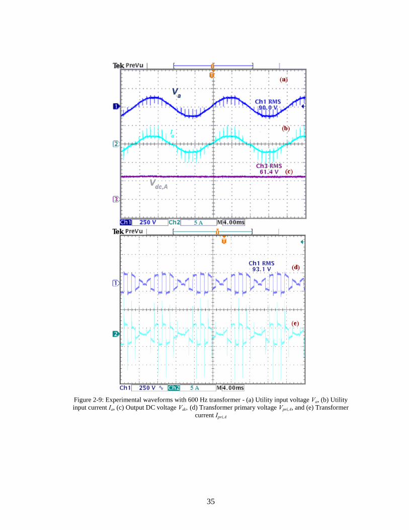
35
Figure 2-9: Experimental waveforms with 600 Hz transformer - (a) Utility input voltage Va, (b) Utility
input current Ia, (c) Output DC voltage Vdc, (d) Transformer primary voltage Vpri,A, and (e) Transformer
current Ipri,A
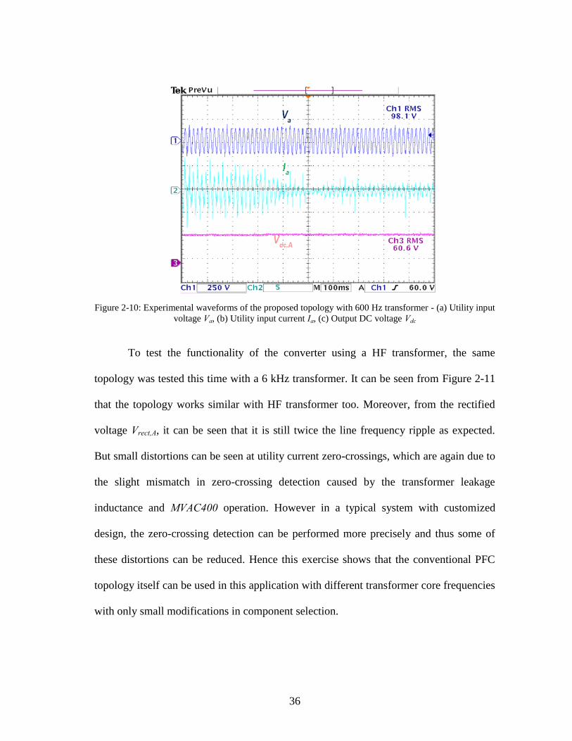
36
Figure 2-10: Experimental waveforms of the proposed topology with 600 Hz transformer - (a) Utility input
voltage Va, (b) Utility input current Ia, (c) Output DC voltage Vdc
To test the functionality of the converter using a HF transformer, the same
topology was tested this time with a 6 kHz transformer. It can be seen from Figure 2-11
that the topology works similar with HF transformer too. Moreover, from the rectified
voltage Vrect,A, it can be seen that it is still twice the line frequency ripple as expected.
But small distortions can be seen at utility current zero-crossings, which are again due to
the slight mismatch in zero-crossing detection caused by the transformer leakage
inductance and MVAC400 operation. However in a typical system with customized
design, the zero-crossing detection can be performed more precisely and thus some of
these distortions can be reduced. Hence this exercise shows that the conventional PFC
topology itself can be used in this application with different transformer core frequencies
with only small modifications in component selection.
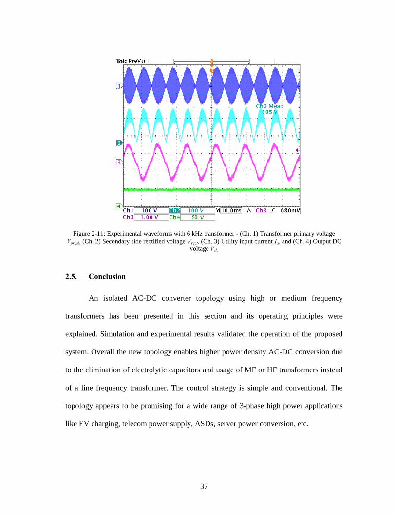
37
Figure 2-11: Experimental waveforms with 6 kHz transformer - (Ch. 1) Transformer primary voltage
Vpri,A, (Ch. 2) Secondary side rectified voltage Vrect, (Ch. 3) Utility input current Ia, and (Ch. 4) Output DC
voltage Vdc
2.5. Conclusion
An isolated AC-DC converter topology using high or medium frequency
transformers has been presented in this section and its operating principles were
explained. Simulation and experimental results validated the operation of the proposed
system. Overall the new topology enables higher power density AC-DC conversion due
to the elimination of electrolytic capacitors and usage of MF or HF transformers instead
of a line frequency transformer. The control strategy is simple and conventional. The
topology appears to be promising for a wide range of 3-phase high power applications
like EV charging, telecom power supply, ASDs, server power conversion, etc.
38
3. SIMPLIFIED MEDIUM/HIGH FREQUENCY
TRANSFORMER BASED MULTI-PULSE DIODE RECTIFIERS
Introduction to Adjustable Speed Drives and Multi-Pulse Rectifiers 3.1.
Electric motors are an integral part of modern life and industrial production.
There are more than 300 million motors installed worldwide in industries including oil
and gas, petrochemicals, cement, transportation, steel and other heavy manufacturing.
This figure grows each year by more than 10% and it is estimated that the motor market
around the world will exceed US$ 60 billion by the year 2017. Advanced inverter
configurations such as Variable Speed Drive (VSD) and Adjustable Speed Drive (ASD)
have facilitated easier speed and torque control of AC motors and contribute to
significant energy savings [42]. The introduction of improved power electronic
topologies, development of robust motor-control techniques, and advancements in state-
of-the-art semiconductor technologies like fast-switching silicon carbide (SiC) wide-
band gap power devices have helped in precision regulation of speed and position [43,
44]. The aforementioned developments in ASDs offer several benefits, such as energy
savings, improved process control, improved system reliability and smoother operation
[13]. Further improvements in the design of power electronic inverters, utility grid
interface transformers, and electric motors could reduce the cost and size of these
systems and offer total savings of up to US$ 2 trillion in two decades [13].
ASDs offer several benefits, some of which are relatively easy to quantify and
others of which are less tangible. The major advantages are energy savings, improved
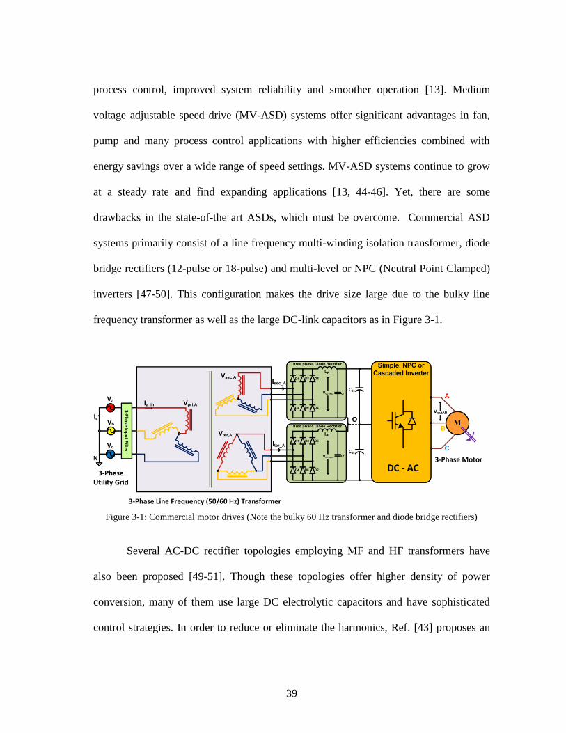
39
process control, improved system reliability and smoother operation [13]. Medium
voltage adjustable speed drive (MV-ASD) systems offer significant advantages in fan,
pump and many process control applications with higher efficiencies combined with
energy savings over a wide range of speed settings. MV-ASD systems continue to grow
at a steady rate and find expanding applications [13, 44-46]. Yet, there are some
drawbacks in the state-of-the art ASDs, which must be overcome. Commercial ASD
systems primarily consist of a line frequency multi-winding isolation transformer, diode
bridge rectifiers (12-pulse or 18-pulse) and multi-level or NPC (Neutral Point Clamped)
inverters [47-50]. This configuration makes the drive size large due to the bulky line
frequency transformer as well as the large DC-link capacitors as in Figure 3-1.
Figure 3-1: Commercial motor drives (Note the bulky 60 Hz transformer and diode bridge rectifiers)
Several AC-DC rectifier topologies employing MF and HF transformers have
also been proposed [49-51]. Though these topologies offer higher density of power
conversion, many of them use large DC electrolytic capacitors and have sophisticated
control strategies. In order to reduce or eliminate the harmonics, Ref. [43] proposes an
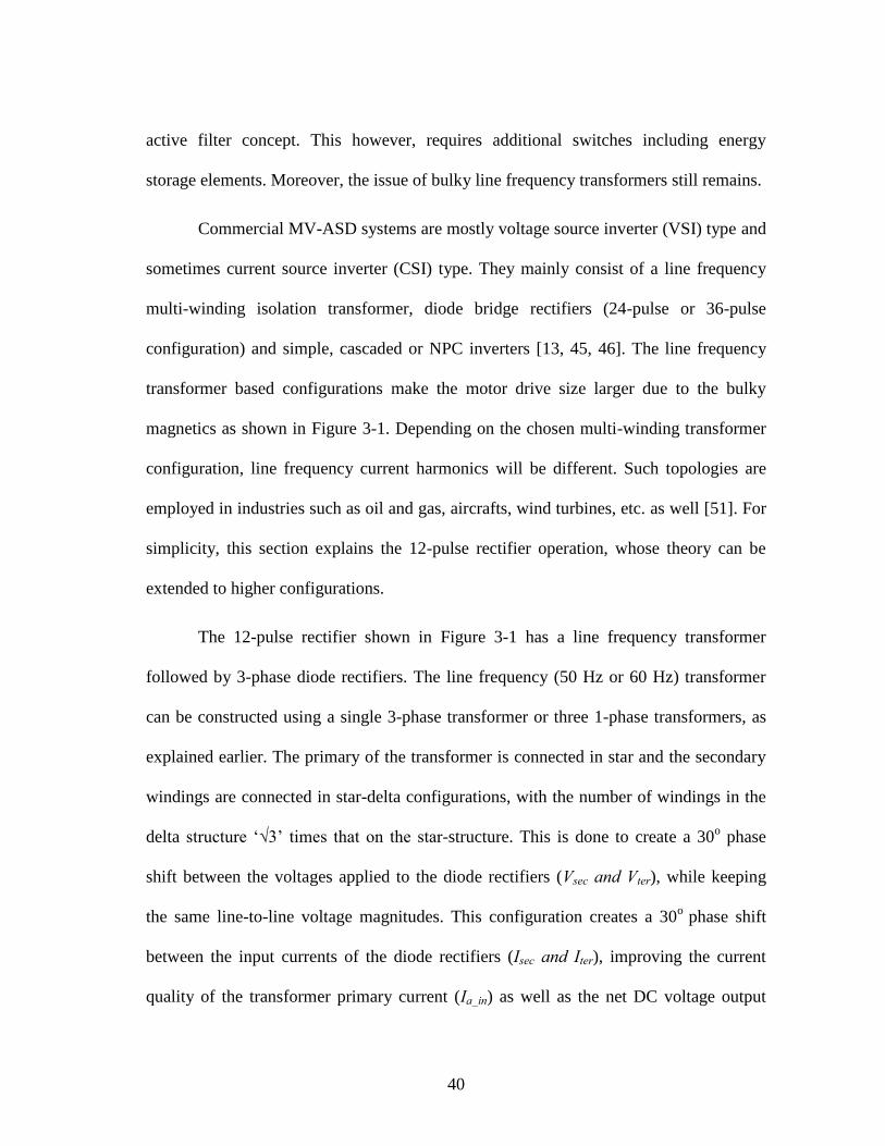
40
active filter concept. This however, requires additional switches including energy
storage elements. Moreover, the issue of bulky line frequency transformers still remains.
Commercial MV-ASD systems are mostly voltage source inverter (VSI) type and
sometimes current source inverter (CSI) type. They mainly consist of a line frequency
multi-winding isolation transformer, diode bridge rectifiers (24-pulse or 36-pulse
configuration) and simple, cascaded or NPC inverters [13, 45, 46]. The line frequency
transformer based configurations make the motor drive size larger due to the bulky
magnetics as shown in Figure 3-1. Depending on the chosen multi-winding transformer
configuration, line frequency current harmonics will be different. Such topologies are
employed in industries such as oil and gas, aircrafts, wind turbines, etc. as well [51]. For
simplicity, this section explains the 12-pulse rectifier operation, whose theory can be
extended to higher configurations.
The 12-pulse rectifier shown in Figure 3-1 has a line frequency transformer
followed by 3-phase diode rectifiers. The line frequency (50 Hz or 60 Hz) transformer
can be constructed using a single 3-phase transformer or three 1-phase transformers, as
explained earlier. The primary of the transformer is connected in star and the secondary
windings are connected in star-delta configurations, with the number of windings in the
delta structure ‘√3’ times that on the star-structure. This is done to create a 30o phase
shift between the voltages applied to the diode rectifiers (Vsec and Vter), while keeping
the same line-to-line voltage magnitudes. This configuration creates a 30o
phase shift
between the input currents of the diode rectifiers (Isec and Iter), improving the current
quality of the transformer primary current (Ia_in) as well as the net DC voltage output
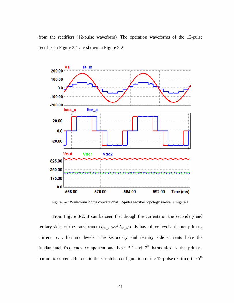
41
from the rectifiers (12-pulse waveform). The operation waveforms of the 12-pulse
rectifier in Figure 3-1 are shown in Figure 3-2.
Figure 3-2: Waveforms of the conventional 12-pulse rectifier topology shown in Figure 1.
From Figure 3-2, it can be seen that though the currents on the secondary and
tertiary sides of the transformer (Isec_a and Iter_a) only have three levels, the net primary
current, Ia_in has six levels. The secondary and tertiary side currents have the
fundamental frequency component and have 5th
and 7th
harmonics as the primary
harmonic content. But due to the star-delta configuration of the 12-pulse rectifier, the 5th
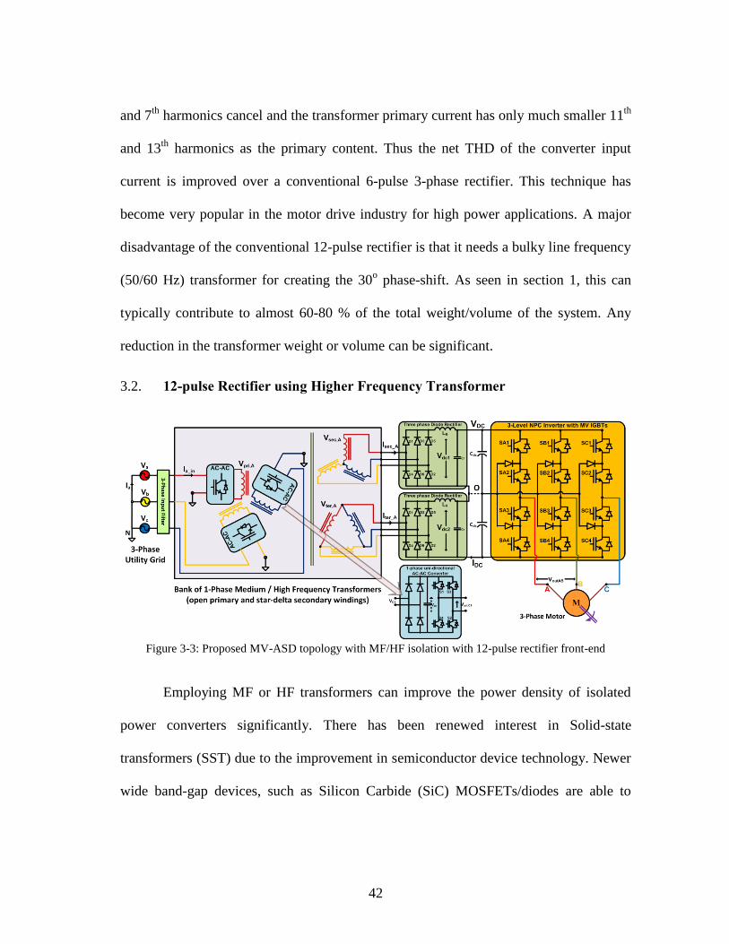
42
and 7th
harmonics cancel and the transformer primary current has only much smaller 11th
and 13th
harmonics as the primary content. Thus the net THD of the converter input
current is improved over a conventional 6-pulse 3-phase rectifier. This technique has
become very popular in the motor drive industry for high power applications. A major
disadvantage of the conventional 12-pulse rectifier is that it needs a bulky line frequency
(50/60 Hz) transformer for creating the 30o phase-shift. As seen in section 1, this can
typically contribute to almost 60-80 % of the total weight/volume of the system. Any
reduction in the transformer weight or volume can be significant.
12-pulse Rectifier using Higher Frequency Transformer 3.2.
Figure 3-3: Proposed MV-ASD topology with MF/HF isolation with 12-pulse rectifier front-end
Employing MF or HF transformers can improve the power density of isolated
power converters significantly. There has been renewed interest in Solid-state
transformers (SST) due to the improvement in semiconductor device technology. Newer
wide band-gap devices, such as Silicon Carbide (SiC) MOSFETs/diodes are able to
43
switch much faster due to lower losses. Based on the voltage and power ratings, different
types of SSTs have been proposed, with frequencies ranging from 1 kHz to 20 kHz [47].
This section introduces a simplified medium frequency (MF) or high frequency
(HF) transformer based multi-pulse rectifier system with unidirectional AC-AC
converters at the input side. The diode bridge rectifier on the transformer secondary side
and NPC inverter look similar to the conventional approach. Figure 3-3 shows the
proposed topology. AC-AC converters are employed on the utility input side to convert
the 50/60Hz line frequency voltage to higher frequency AC. The output of the AC-AC
converters is then interfaced with medium/high frequency (MF/HF) transformer
constructed with electrical steel or other advanced low loss magnetic materials. The
secondary of the transformer constitute standard multi-pulse windings that power the
rectifier DC-link, inverter systems.
Figure 3-4: Proposed Medium Voltage ASD with series-stacked/cascaded AC-AC converter structure
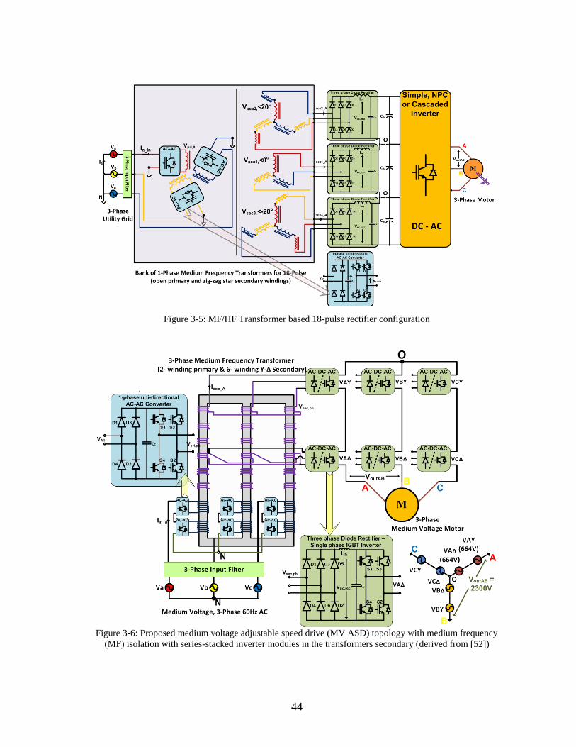
44
Figure 3-5: MF/HF Transformer based 18-pulse rectifier configuration
Figure 3-6: Proposed medium voltage adjustable speed drive (MV ASD) topology with medium frequency
(MF) isolation with series-stacked inverter modules in the transformers secondary (derived from [52])
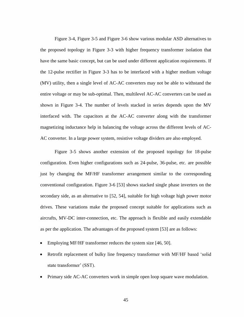
45
Figure 3-4, Figure 3-5 and Figure 3-6 show various modular ASD alternatives to
the proposed topology in Figure 3-3 with higher frequency transformer isolation that
have the same basic concept, but can be used under different application requirements. If
the 12-pulse rectifier in Figure 3-3 has to be interfaced with a higher medium voltage
(MV) utility, then a single level of AC-AC converters may not be able to withstand the
entire voltage or may be sub-optimal. Then, multilevel AC-AC converters can be used as
shown in Figure 3-4. The number of levels stacked in series depends upon the MV
interfaced with. The capacitors at the AC-AC converter along with the transformer
magnetizing inductance help in balancing the voltage across the different levels of AC-
AC converter. In a large power system, resistive voltage dividers are also employed.
Figure 3-5 shows another extension of the proposed topology for 18-pulse
configuration. Even higher configurations such as 24-pulse, 36-pulse, etc. are possible
just by changing the MF/HF transformer arrangement similar to the corresponding
conventional configuration. Figure 3-6 [53] shows stacked single phase inverters on the
secondary side, as an alternative to [52, 54], suitable for high voltage high power motor
drives. These variations make the proposed concept suitable for applications such as
aircrafts, MV-DC inter-connection, etc. The approach is flexible and easily extendable
as per the application. The advantages of the proposed system [53] are as follows:
Employing MF/HF transformer reduces the system size [46, 50].
Retrofit replacement of bulky line frequency transformer with MF/HF based ‘solid
state transformer’ (SST).
Primary side AC-AC converters work in simple open loop square wave modulation.

46
Use of wide band-gap SiC power semiconductor devices at high frequencies, along
with amorphous/ferrite core transformer will further enhance the system efficiencies.
Passive components including the input filter, DC bus capacitor, etc. can be designed
in a similar way as in a typical 12-pulse or higher pulse rectifier system.
The use of series stacked AC-AC converters for generating medium/high frequency
is inherently fault tolerant. Under converter fault conditions, one or more of the
series stacked AC-AC converter modules can be actively by-passed.
As discussed, the proposed concept can be extended to 18-pulse, 24-pulse and
other configurations as well, but this section focuses on design, working principle,
simulation and experiments on 12-pulse rectifier system for simplicity in explanation
and demonstration, considering the operation of higher configurations can be deduced
from this system. Moreover, the focus of this section is on the front-end of an ASD
system, so the inverter operation is not discussed in detail. The inverter is assumed to be
similar to the ones in conventional ASDs, which can be simple, NPC or cascaded. The
Figure 3-3 shows the motor drive inverter as a 3-level NPC structure. The design of the
front-end of the proposed ASD system can be mainly divided into the following sub-
sections: (i) AC-AC converter, (ii) 3-phase diode rectifier, (iii) HF or MF transformer,
and (iv) Passive components.
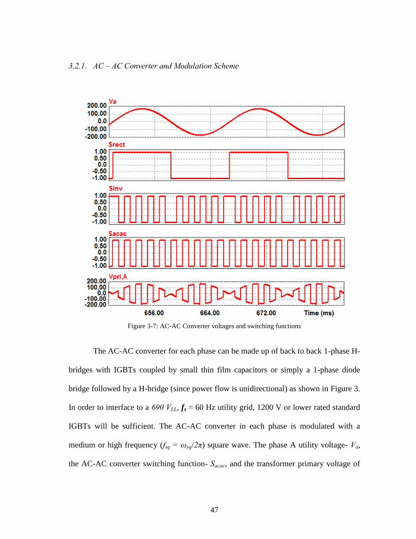
47
3.2.1. AC – AC Converter and Modulation Scheme
Figure 3-7: AC-AC Converter voltages and switching functions
The AC-AC converter for each phase can be made up of back to back 1-phase H-
bridges with IGBTs coupled by small thin film capacitors or simply a 1-phase diode
bridge followed by a H-bridge (since power flow is unidirectional) as shown in Figure 3.
In order to interface to a 690 VLL, fs = 60 Hz utility grid, 1200 V or lower rated standard
IGBTs will be sufficient. The AC-AC converter in each phase is modulated with a
medium or high frequency (fsq = ωsq/2π) square wave. The phase A utility voltage- Va,
the AC-AC converter switching function- Sacac, and the transformer primary voltage of

48
phase A- Vpri,A, can be given by eqns. (2.1), (2.2) and (2.3) discussed in section 2.2.1.
The modulating square wave must be synchronized across the three phases. This is done
in order to make the net flux balanced on the primary side of the transformer, which can
be achieved if the net sum of primary voltages Vpri,A + Vpri,B + Vpri,C is equal to zero
(= 0) at every instant.
The voltage fed to the transformer primary has a sinusoidal envelope that is
obtained by multiplying the utility sinusoidal voltage and a HF/MF square wave. From
(3), it can be seen that the transformer primary voltage Vpri,a has frequency components
only around the square wave switching frequency, fsq and not at low frequencies. This
enables the use of HF or MF transformers, hence reducing the system size. Further, even
if the frequency of AC input (Va) varies slightly, the transformer operating frequency
does not change much. This property makes the proposed topologies (with slight
extensions) attractive for applications where the input frequency can vary over a wide
range. It should be noted that the switching function of the AC-AC converter overall,
represented as Sacac in eqn. (2), is MF/HF square wave. But the diode rectifier section of
the AC-AC converter introduces a switching function of a line frequency square wave
(Srect), which must be compensated in the modulation of the H-bridge (Sinv) of the AC-
AC converter by multiplying the MF square switching function Sacac with the diode
rectifier switching function. These waveforms are shown in Figure 3-7.
One of the major advantages of the proposed concept is the simplicity in the
modulation scheme. No closed loop control scheme is required for the front-end since
the topology intends to replicate the performance of a conventional line frequency
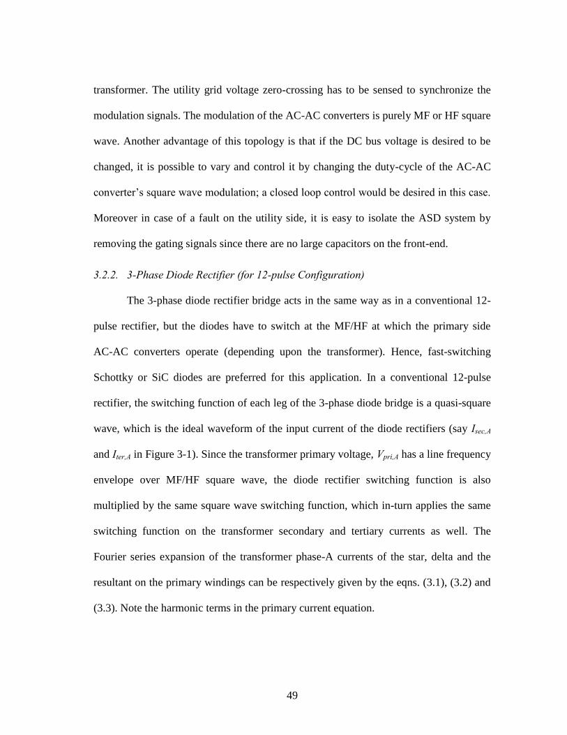
49
transformer. The utility grid voltage zero-crossing has to be sensed to synchronize the
modulation signals. The modulation of the AC-AC converters is purely MF or HF square
wave. Another advantage of this topology is that if the DC bus voltage is desired to be
changed, it is possible to vary and control it by changing the duty-cycle of the AC-AC
converter’s square wave modulation; a closed loop control would be desired in this case.
Moreover in case of a fault on the utility side, it is easy to isolate the ASD system by
removing the gating signals since there are no large capacitors on the front-end.
3.2.2. 3-Phase Diode Rectifier (for 12-pulse Configuration)
The 3-phase diode rectifier bridge acts in the same way as in a conventional 12-
pulse rectifier, but the diodes have to switch at the MF/HF at which the primary side
AC-AC converters operate (depending upon the transformer). Hence, fast-switching
Schottky or SiC diodes are preferred for this application. In a conventional 12-pulse
rectifier, the switching function of each leg of the 3-phase diode bridge is a quasi-square
wave, which is the ideal waveform of the input current of the diode rectifiers (say Isec,A
and Iter,A in Figure 3-1). Since the transformer primary voltage, Vpri,A has a line frequency
envelope over MF/HF square wave, the diode rectifier switching function is also
multiplied by the same square wave switching function, which in-turn applies the same
switching function on the transformer secondary and tertiary currents as well. The
Fourier series expansion of the transformer phase-A currents of the star, delta and the
resultant on the primary windings can be respectively given by the eqns. (3.1), (3.2) and
(3.3). Note the harmonic terms in the primary current equation.
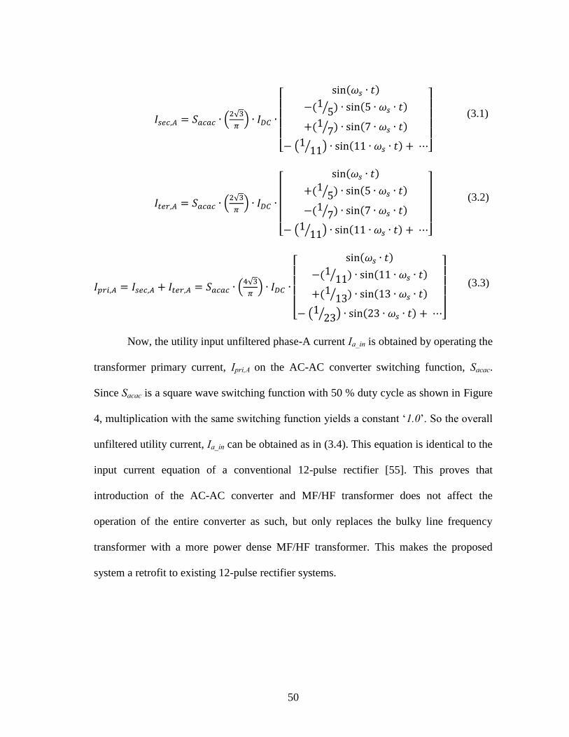
50
𝐼𝑠𝑒𝑐,𝐴 = 𝑆𝑎𝑐𝑎𝑐 ∙ (2√3
𝜋) ∙ 𝐼𝐷𝐶 ∙
[
sin(𝜔𝑠 ∙ 𝑡)
−(1 5⁄ ) ∙ sin(5 ∙ 𝜔𝑠 ∙ 𝑡)
+(1 7⁄ ) ∙ sin(7 ∙ 𝜔𝑠 ∙ 𝑡)
− (1 11⁄ ) ∙ sin(11 ∙ 𝜔𝑠 ∙ 𝑡) + ⋯]
𝐼𝑡𝑒𝑟,𝐴 = 𝑆𝑎𝑐𝑎𝑐 ∙ (2√3
𝜋) ∙ 𝐼𝐷𝐶 ∙
[
sin(𝜔𝑠 ∙ 𝑡)
+(1 5⁄ ) ∙ sin(5 ∙ 𝜔𝑠 ∙ 𝑡)
−(1 7⁄ ) ∙ sin(7 ∙ 𝜔𝑠 ∙ 𝑡)
− (1 11⁄ ) ∙ sin(11 ∙ 𝜔𝑠 ∙ 𝑡) + ⋯]
𝐼𝑝𝑟𝑖,𝐴 = 𝐼𝑠𝑒𝑐,𝐴 + 𝐼𝑡𝑒𝑟,𝐴 = 𝑆𝑎𝑐𝑎𝑐 ∙ (4√3
𝜋) ∙ 𝐼𝐷𝐶 ∙
[
sin(𝜔𝑠 ∙ 𝑡)
−(1 11⁄ ) ∙ sin(11 ∙ 𝜔𝑠 ∙ 𝑡)
+(1 13⁄ ) ∙ sin(13 ∙ 𝜔𝑠 ∙ 𝑡)
− (1 23⁄ ) ∙ sin(23 ∙ 𝜔𝑠 ∙ 𝑡) + ⋯]
Now, the utility input unfiltered phase-A current Ia_in is obtained by operating the
transformer primary current, Ipri,A on the AC-AC converter switching function, Sacac.
Since Sacac is a square wave switching function with 50 % duty cycle as shown in Figure
4, multiplication with the same switching function yields a constant ‘1.0’. So the overall
unfiltered utility current, Ia_in can be obtained as in (3.4). This equation is identical to the
input current equation of a conventional 12-pulse rectifier [55]. This proves that
introduction of the AC-AC converter and MF/HF transformer does not affect the
operation of the entire converter as such, but only replaces the bulky line frequency
transformer with a more power dense MF/HF transformer. This makes the proposed
system a retrofit to existing 12-pulse rectifier systems.
(3.1)
(3.2)
(3.3)

51
𝐼𝑎_𝑖𝑛 = (4√3
𝜋) ∙ 𝐼𝐷𝐶 ∙
[
sin(𝜔𝑠 ∙ 𝑡)
−(1 11⁄ ) ∙ sin(11 ∙ 𝜔𝑠 ∙ 𝑡)
+(1 13⁄ ) ∙ sin(13 ∙ 𝜔𝑠 ∙ 𝑡)
− (1 23⁄ ) ∙ sin(23 ∙ 𝜔𝑠 ∙ 𝑡) + ⋯]
3.2.3. Medium Frequency (MF) or High Frequency (HF) Transformer
As discussed earlier, based on the required power density and efficiency, the
transformer can be designed with conventional silicon steel or amorphous cores to
operate at a MF (400 Hz to 2 kHz) or at HF (5 kHz to 20 kHz). It may be noted that
since the audible noise is typically high for the frequency range between 2 kHz and 5
kHz, it becomes physically challenging to design the transformer core in that range. For
high power applications, MF is desired since the converter switching loss can increase
significantly is operated at high frequencies. The construction is otherwise similar to the
line frequency transformer in a typical 12-pulse rectifier. If three 1-phase transformers
are used, they should have three windings on each transformer with the turns ratio –
Npri:Nsec:Nter = 1:1:√3 as in the conventional system shown in Figure 3-1. The
transformer also needs to handle the harmonic currents that flow through primary,
secondary and tertiary windings. Detailed transformer design is covered in section 6.
3.2.4. Passive Components and Filter Design
The input LC filter is designed similar to the corresponding multi-pulse
rectifier’s typical filter design since the input currents will have similar harmonics
(fundamental, 11th, 13th, etc.). The input filter can be designed at around 400 Hz cut-off
(3.4)
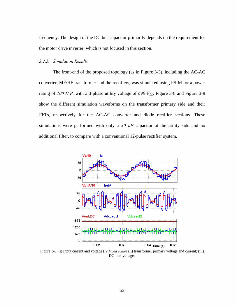
52
frequency. The design of the DC bus capacitor primarily depends on the requirement for
the motor drive inverter, which is not focused in this section.
3.2.5. Simulation Results
The front-end of the proposed topology (as in Figure 3-3), including the AC-AC
converter, MF/HF transformer and the rectifiers, was simulated using PSIM for a power
rating of 100 H.P. with a 3-phase utility voltage of 690 VLL. Figure 3-8 and Figure 3-9
show the different simulation waveforms on the transformer primary side and their
FFTs, respectively for the AC-AC converter and diode rectifier sections. These
simulations were performed with only a 30 uF capacitor at the utility side and no
additional filter, to compare with a conventional 12-pulse rectifier system.
Figure 3-8: (i) Input current and voltage (reduced scale) (ii) transformer primary voltage and current; (iii)
DC-link voltages
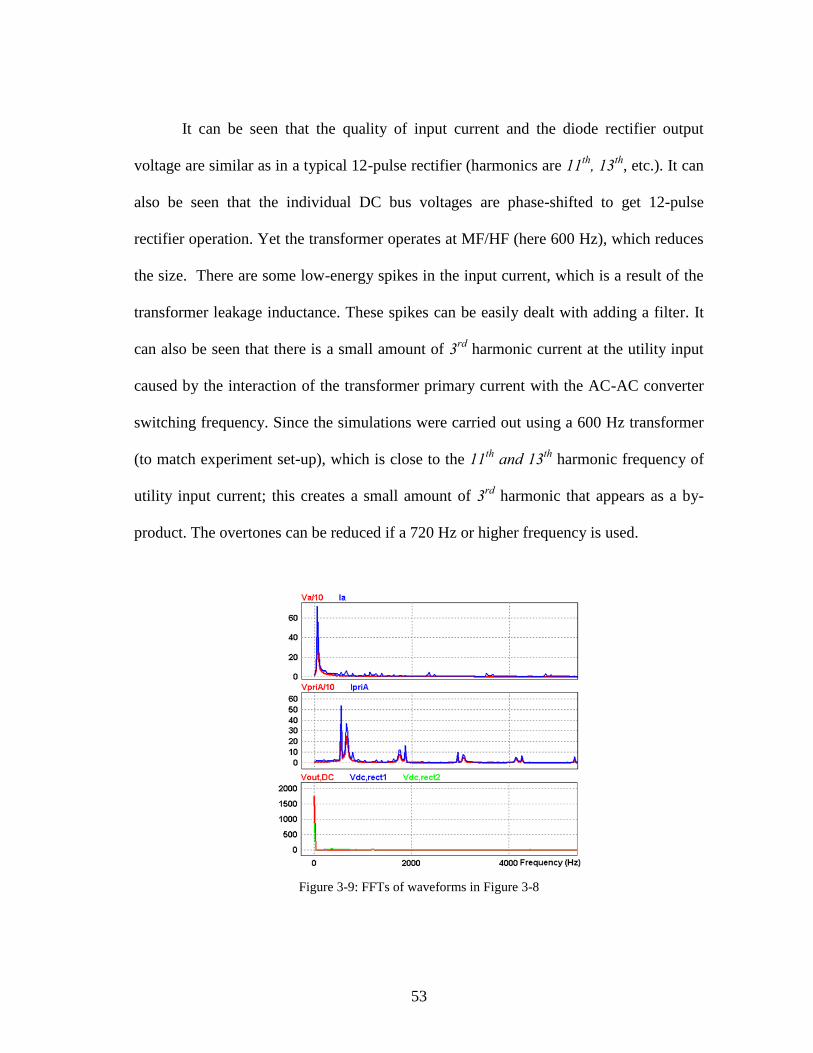
53
It can be seen that the quality of input current and the diode rectifier output
voltage are similar as in a typical 12-pulse rectifier (harmonics are 11th, 13th, etc.). It can
also be seen that the individual DC bus voltages are phase-shifted to get 12-pulse
rectifier operation. Yet the transformer operates at MF/HF (here 600 Hz), which reduces
the size. There are some low-energy spikes in the input current, which is a result of the
transformer leakage inductance. These spikes can be easily dealt with adding a filter. It
can also be seen that there is a small amount of 3rd harmonic current at the utility input
caused by the interaction of the transformer primary current with the AC-AC converter
switching frequency. Since the simulations were carried out using a 600 Hz transformer
(to match experiment set-up), which is close to the 11th and 13th harmonic frequency of
utility input current; this creates a small amount of 3rd harmonic that appears as a by-
product. The overtones can be reduced if a 720 Hz or higher frequency is used.
Figure 3-9: FFTs of waveforms in Figure 3-8
54
From Figure 3-10, the phase shift between the transformer secondary voltages
and currents are evident. Transformer primary current is the result of sum of the
secondary and tertiary currents. From the graph (iii) in Figure 3-10, it can be seen that
the secondary and tertiary currents, when operated on by the AC-AC converter switching
function, look similar to the ones in a conventional 12-pulse rectifier system. This
enables the input utility current to have similar features as in the conventional system.
Figure 3-10: Simulation waveforms at the transformer - (i) Primary voltage (reduced scale) and current,
(ii) Secondary and tertiary line-to-line voltages; (iii) Secondary and tertiary diode rectifier input currents
3.2.6. Experimental Results
Based on the simulation results and the transformer designs done earlier,
experiments were conducted on a scaled down laboratory prototype of 1 kW 12-pulse
rectifier configuration. Similar to the simulation results, experiments were conducted
with and without input filter. Three 1-phase 600 Hz transformers were used for the
experiments, whose secondary and tertiary windings were connected in star-delta
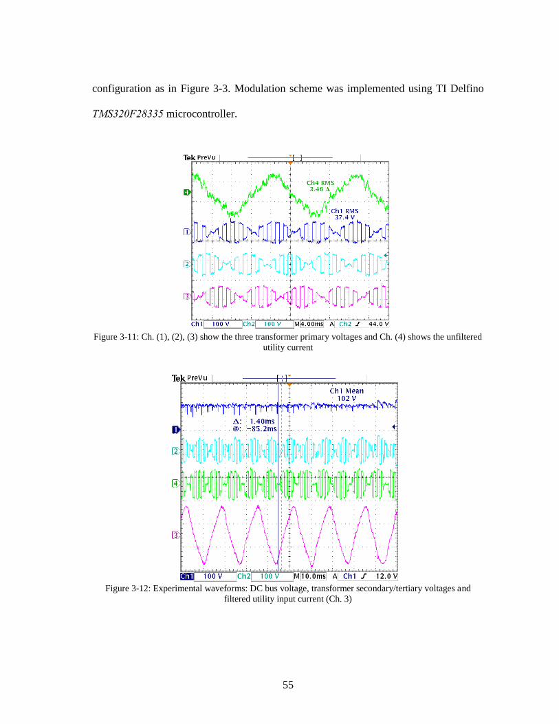
55
configuration as in Figure 3-3. Modulation scheme was implemented using TI Delfino
TMS320F28335 microcontroller.
Figure 3-11: Ch. (1), (2), (3) show the three transformer primary voltages and Ch. (4) shows the unfiltered
utility current
Figure 3-12: Experimental waveforms: DC bus voltage, transformer secondary/tertiary voltages and
filtered utility input current (Ch. 3)
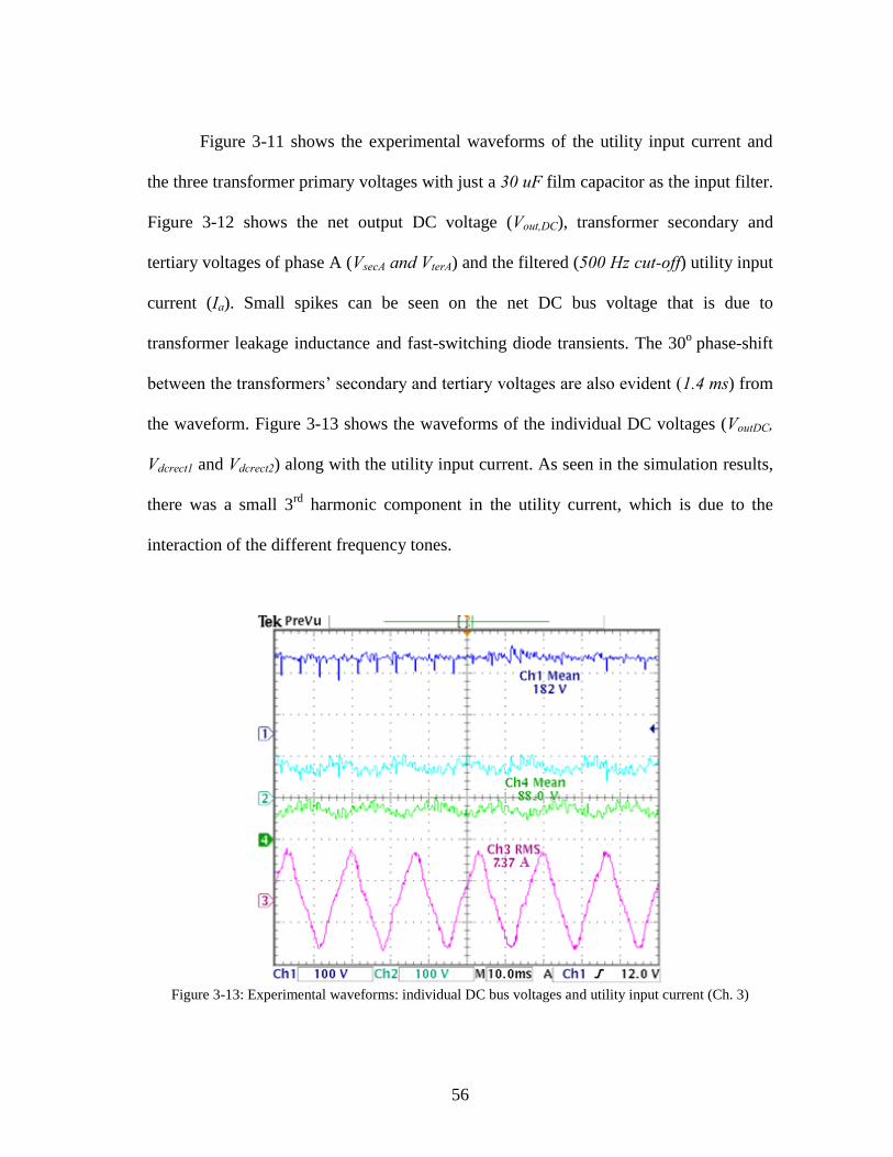
56
Figure 3-11 shows the experimental waveforms of the utility input current and
the three transformer primary voltages with just a 30 uF film capacitor as the input filter.
Figure 3-12 shows the net output DC voltage (Vout,DC), transformer secondary and
tertiary voltages of phase A (VsecA and VterA) and the filtered (500 Hz cut-off) utility input
current (Ia). Small spikes can be seen on the net DC bus voltage that is due to
transformer leakage inductance and fast-switching diode transients. The 30o
phase-shift
between the transformers’ secondary and tertiary voltages are also evident (1.4 ms) from
the waveform. Figure 3-13 shows the waveforms of the individual DC voltages (VoutDC,
Vdcrect1 and Vdcrect2) along with the utility input current. As seen in the simulation results,
there was a small 3rd
harmonic component in the utility current, which is due to the
interaction of the different frequency tones.
Figure 3-13: Experimental waveforms: individual DC bus voltages and utility input current (Ch. 3)

57
MF Transformer based ASD Topology with PWM Front-End 3.3.
In this sub-section a medium frequency transformer with AC-AC converters at
the input side is shown to obtain good input current performance with simultaneous
reduction in size, weight and volume, especially for lower voltage 3-phase utility (480
VLL, 690 VLL, etc.). The transformer primary side structure is similar to the one explained
in the previous sub-section (see Figure 3-3). An AC-AC converter using bidirectional
switches (see Figure 1-10) is more suitable than the unidirectional AC-AC converter if
operated at high PWM frequencies. The AC-AC converter gating signals are generated
by a product of unipolar line frequency sine PWM and a MF square function. The
modulation strategy is flexible and allows for higher PWM switching frequency
operation of the AC-AC converter, while ensuring that the transformer core is operated
at MF over the entire range of operation. The secondary side of the transformer is delta-
connected to a 6-pulse rectifier, with a simple or NPC motor drive inverter as discussed
earlier. Here, the filter sizes are smaller due to the use of higher frequency PWM. The
main features of the proposed system in Figure 3-14 are as follows:
• The input current harmonics are of higher order, at least twice the MF; therefore the
input filter size is smaller.
• The secondary side diode rectifier output is of higher-quality as well.
• Since PWM operating frequency has to be at least 3 - 4 times that of the MF, the
power converter losses are higher than the earlier case with square wave modulation.
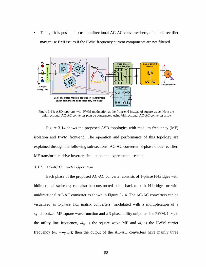
58
• Though it is possible to use unidirectional AC-AC converter here, the diode rectifier
may cause EMI issues if the PWM frequency current components are not filtered.
Figure 3-14: ASD topology with PWM modulation at the front-end instead of square wave. Note the
unidirectional AC-AC converter (can be constructed using bidirectional AC-AC converter also)
Figure 3-14 shows the proposed ASD topologies with medium frequency (MF)
isolation and PWM front-end. The operation and performance of this topology are
explained through the following sub-sections: AC-AC converter, 3-phase diode rectifier,
MF transformer, drive inverter, simulation and experimental results.
3.3.1. AC-AC Converter Operation
Each phase of the proposed AC-AC converter consists of 1-phase H-bridges with
bidirectional switches; can also be constructed using back-to-back H-bridges or with
unidirectional AC-AC converter as shown in Figure 3-14. The AC-AC converters can be
visualized as 1-phase 1x1 matrix converters, modulated with a multiplication of a
synchronized MF square wave function and a 3-phase utility unipolar sine PWM. If ωs is
the utility line frequency, ωsq is the square wave MF and ωc is the PWM carrier
frequency (ωc =mf.ωs); then the output of the AC-AC converters have mainly three
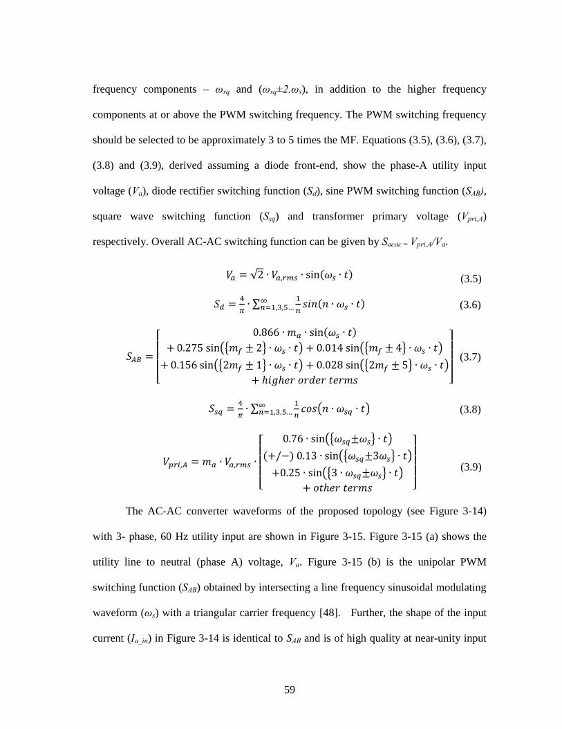
59
frequency components – ωsq and (ωsq±2.ωs), in addition to the higher frequency
components at or above the PWM switching frequency. The PWM switching frequency
should be selected to be approximately 3 to 5 times the MF. Equations (3.5), (3.6), (3.7),
(3.8) and (3.9), derived assuming a diode front-end, show the phase-A utility input
voltage (Va), diode rectifier switching function (Sd), sine PWM switching function (SAB),
square wave switching function (Ssq) and transformer primary voltage (Vpri,A)
respectively. Overall AC-AC switching function can be given by Sacac = Vpri,A/Va.
𝑉𝑎 = √2 ∙ 𝑉𝑎,𝑟𝑚𝑠 ∙ sin(𝜔𝑠 ∙ 𝑡)
𝑆𝑑 =4
𝜋∙ ∑
1
𝑛
∞𝑛=1,3,5… 𝑠𝑖𝑛(𝑛 ∙ 𝜔𝑠 ∙ 𝑡)
𝑆𝐴𝐵 =
[
0.866 ∙ 𝑚𝑎 ∙ sin(𝜔𝑠 ∙ 𝑡)
+ 0.275 sin({𝑚𝑓 ± 2} ∙ 𝜔𝑠 ∙ 𝑡) + 0.014 sin({𝑚𝑓 ± 4} ∙ 𝜔𝑠 ∙ 𝑡)
+0.156 sin({2𝑚𝑓 ± 1} ∙ 𝜔𝑠 ∙ 𝑡) + 0.028 sin({2𝑚𝑓 ± 5} ∙ 𝜔𝑠 ∙ 𝑡)
+ ℎ𝑖𝑔ℎ𝑒𝑟 𝑜𝑟𝑑𝑒𝑟 𝑡𝑒𝑟𝑚𝑠 ]
𝑆𝑠𝑞 =4
𝜋∙ ∑
1
𝑛
∞𝑛=1,3,5… 𝑐𝑜𝑠(𝑛 ∙ 𝜔𝑠𝑞 ∙ 𝑡)
𝑉𝑝𝑟𝑖,𝐴 = 𝑚𝑎 ∙ 𝑉𝑎,𝑟𝑚𝑠 ∙
[
0.76 ∙ sin({𝜔𝑠𝑞±𝜔𝑠} ∙ 𝑡)
(+/−) 0.13 ∙ sin({𝜔𝑠𝑞±3𝜔𝑠} ∙ 𝑡)
+0.25 ∙ sin({3 ∙ 𝜔𝑠𝑞±𝜔𝑠} ∙ 𝑡)
+ 𝑜𝑡ℎ𝑒𝑟 𝑡𝑒𝑟𝑚𝑠 ]
The AC-AC converter waveforms of the proposed topology (see Figure 3-14)
with 3- phase, 60 Hz utility input are shown in Figure 3-15. Figure 3-15 (a) shows the
utility line to neutral (phase A) voltage, Va. Figure 3-15 (b) is the unipolar PWM
switching function (SAB) obtained by intersecting a line frequency sinusoidal modulating
waveform (ωs) with a triangular carrier frequency [48]. Further, the shape of the input
current (Ia_in) in Figure 3-14 is identical to SAB and is of high quality at near-unity input
(3.7)
(3.5)
(3.8)
(3.9)
(3.6)

60
power factor. It can also be seen from Figure 3-15 (d) that the transformer secondary
voltage has the envelope of sine PWM as well as that of the MF square wave.
Figure 3-15: AC-AC converter waveforms from Figure 3 topology. (a) Input grid voltage and current, (b)
Unipolar Sine PWM switching function, (c) Square wave switching function and (d) Transformer
secondary voltage
3.3.2. Three-Phase Diode Rectifier
Since the 3-phase diode rectifier is connected across a delta winding, the
operation of the rectifiers is governed directly by the primary side phase voltages. In this
case, the transformer primary voltage is a product of MF square wave and unipolar sine
PWM, which makes the diode rectifier operate like a PWM rectifier. This PWM
property enables this topology to eventually make the utility input current of high
quality. But it should be noted that since the diodes operate at the PWM frequency, fast-
switching SiC or fast-recovery diodes must be used to reduce the switching losses.

61
If IDC is the DC-link current, which is the output of the 3-phase rectifier, and
assuming that the ripple on IDC is negligible, then the diode rectifier behaves like a PWM
rectifier, as discussed above; but the MF square wave modulation super-imposes the
PWM rectifier switching function (3.7) with a MF square-wave function (3.8). So, the
transformer primary (or secondary) current can be given by (3.10), assuming unity MF
transformer turns-ratio. Now, the unfiltered utility input phase-A current, Ia_in, can be
derived by operating the AC-AC converter switching function, Sacac, over the
transformer primary current, Ipri,A (other phase currents can be derived in a similar way).
The input current equation (unfiltered) can be given by (3.11). The 3-phase rectifier DC
voltage (unfiltered) can be derived using (3.12). From (3.11), it is clear that the utility
input current has the fundamental, followed by harmonics close to PWM switching
frequency, so it is of better quality, compared to the proposed topology in Figure 3-3.
But this scheme also has a small 3rd
harmonic frequency components (around 8 %)
generated as a by-product of the switching functions and can be filtered by an L-C filter.
𝐼𝑝𝑟𝑖,𝐴 =𝐼𝐷𝐶
𝑚𝑎∙
[
0.55 ∙ sin({𝜔𝑠𝑞±𝜔𝑠} ∙ 𝑡)
+0.18 ∙ sin({3 ∙ 𝜔𝑠𝑞±𝜔𝑠} ∙ 𝑡)
+0.11 ∙ sin({5 ∙ 𝜔𝑠𝑞±𝜔𝑠} ∙ 𝑡)
+ 𝑜𝑡ℎ𝑒𝑟 𝑡𝑒𝑟𝑚𝑠 ]
𝐼𝑎_𝑖𝑛~ =𝐼𝐷𝐶
𝑚𝑎∙
[
0.93 ∙ sin({𝜔𝑠} ∙ 𝑡)
(+/−)0.23 ∙ sin({𝑚𝑓 ± 2} ∙ 𝜔𝑠 ∙ 𝑡)
(+/−) 0.08 ∙ sin({3 ∙ 𝜔𝑠} ∙ 𝑡)
+ 𝑜𝑡ℎ𝑒𝑟 𝑡𝑒𝑟𝑚𝑠 ]
𝑉𝐷𝐶̅̅ ̅̅ ̅ =
9 ∙ 𝑚𝑎
√2 ∙ 𝜋∙ 𝑉𝑎,𝑟𝑚𝑠
(3.10)
(3.11)
(3.12)

62
3.3.3. Medium Frequency Transformer
The MF transformer design is similar to the ones explained earlier. Based on the
diode rectifier and the inverter equations, the minimum transformer turns ratio
(secondary to primary) was calculated as per (3.13). This is considering that the DC-link
voltage reduces to almost 86% of the level that is usually associated with a 3-phase
diode rectifier (1.35.VLL) and that the inverter operates with sine PWM.
𝑁 = (4∙𝜋
9) ∙ (
1
𝑚𝑎∙𝑚𝑖𝑛𝑣) ∙ (
𝑉𝑖𝑛𝑣_𝑎,𝑟𝑚𝑠
𝑉𝑎,𝑟𝑚𝑠)
where ma and minv are the modulation indices of AC-AC converter and inverter,
respectively. Va,rms and Vinv_a,rms are the grid and motor phase voltages, respectively. For
unity modulation indices (peak), the turns-ratio was selected to be 1.0 in the simulations.
3.3.4. ASD with Motor Drive Inverter
Apart from the above explained circuits, the design of the proposed topology
mainly consists of a simple or NPC inverter. The inverter is designed to supply variable
voltage to the motor [45]. Conventional unipolar sinusoidal PWM or space vector PWM
technique can be employed along with V/F control for the speed control of the motor.
While a 2-level inverter is simpler in construction and modulation, NPC inverter
topology presents certain other benefits to the system. First, voltage stress across the
switches is divided into half. Furthermore, output current ripple and
switching/conduction losses are mitigated. From a motor drive perspective, the use of a
PWM-controlled NPC inverter improves dynamic performance, lowers stresses on the
motor bearings/windings, and reduces noise influence on nearby devices. Variable
(3.13)
63
Voltage Variable Frequency (VVVF) is used to control the inverter. In constant torque
applications, magnitude and direction of the motor flux can be locked together in direct
proportion to the ratio of the inverter’s output voltage to its fundamental frequency.
3.3.5. Simulation Results
Figure 3-16: (i) Utility voltage (Va), current (scaled), (ii) Transformer primary voltage (Vpri,A) and current
The proposed topology in Figure 3-14 was simulated using PSIM for a 690 VLL,
60 Hz, 3-phase utility for a 30 H.P. motor drive front-end system. Figure 3-16 shows the
input current, Ia along with input voltage, Va and transformer primary current, Ipri,A along
with the transformer primary voltage, Vpri,A. It can be seen that the input displacement
power factor is close to unity and the input current is of good quality, when a 700 Hz
cut-off input filter was employed. There are small 600 Hz resonances caused due to the
interaction of the filter with the MF (here, 600 Hz) harmonics in the current. Figure 3-17
64
shows the simulation waveforms on the transformer secondary side. It can be seen that
the transformer voltages are of sine PWM shape and the DC-link voltage is maintained
fairly constant that can be supplied to the inverter.
Figure 3-17: (i) Transformer secondary voltage (Vsec,A) and current (scaled); (ii) DC bus voltage, (VDC)
3.3.6. Experimental Results
Laboratory experiments were performed on a 3-phase scaled-down prototype of
the front-end of the system similar to Figure 3-14 (with diode front-end), with the set-up
similar as explained in the previous sub-section (0). Figure 3-18 shows the transformer
phase-A and phase-B voltages along with the utility current and DC output voltage. It
can be seen that the input current is of good quality, but has similar distortions as seen in
the simulation results (see Figure 3-16) caused due to the interaction of filter resonance
with the MF harmonics. It can also be seen that though no DC electrolytic capacitor was
used, the DC-link voltage is also of good quality with an inductive load (almost 5 %
inductance for line frequency).
65
Figure 3-18: Experimental results for the topology in Figure 3-14: (Ch1) Transformer phase-A voltage,
(Ch2) Transformer phase-B voltage, (Ch3) DC voltage with inductive load
Conclusion 3.4.
In this section, a new MF/HF transformer based front-end topology for multi-
pulse rectifiers was proposed, taking a 12-pulse rectifier based ASD application as an
example. The topology consisted of AC-AC converters, MF/HF transformers and 3-
phase diode bridges to replicate the behavior of a conventional 12-pulse or higher pulse
rectifier. This approach could be a retrofit replacement to bulky line frequency
transformers, providing higher power density in multi-pulse rectifier applications.
Though the introduction of AC-AC converters provided many advantages to the system,
it comes with certain implications on efficiency.

66
Another ASD topology/modulation scheme with medium frequency (MF)
transformer isolation was also introduced. The modifications compared to the 12-pulse
rectifier have only the delta windings on the secondary side. The performance of the
overall system has been shown to be good: a) input current is of higher quality, with near
unity PF, b) the DC-link capacitor size is reduced due to better quality rectified voltage,
c) The proposed modulation strategy has been shown to be flexible to allow higher
switching frequency operation of the AC-AC converter while the transformer core is
operated at MF. Several other advantages of the proposed topologies have been
discussed in detail. Experimental results on the medium frequency transformer have
been shown to achieve efficiencies above 97.5 % and can be a good choice for ASD
applications. Further, the overall size and weight of the transformer could be reduced by
more than 50 % with a reduction of more than 60 % on the transformer. Further
reduction in weight/size is possible through the use of better MF transformer core
materials.
67
4. A NEW WIND TURBINE – MEDIUM VOLTAGE DC (MVDC)
INTERCONNECTION
4.1. Introduction to Wind Turbine Generators (WTGs)
The world is entering a new era in energy generation, where the renewable
energy sources such as solar, wind, etc. have started to achieve grid parity in price with
the conventional sources of energy such as coal, oil, natural gas, etc. Driven by
government subsidies and improved technologies, the cost of generation for renewable
energy sources have been constantly falling and may extensively become cheaper than
conventional generation within 2020, even if the government subsidies subside [56, 57].
These studies have further made renewable energy sources, such as wind even more
attractive because of the opportunity to install them on a much wider scale, both
economically as well as technologically.
Wind turbine generators (WTGs) have been traditionally installed as large farms
on the land at locations where winds are steady and sufficiently strong. The WTGs are
usually induction generators (in direct or doubly-fed configurations). As the size of the
WTGs have been growing over the years, increasing their energy harvesting, direct-drive
WTGs are also becoming very popular [58]. The most popular direct power converter
architecture for interfacing WTGs to the utility grid is shown in Figure 4-1. It consists of
a PWM rectifier that converts the variable WTG frequency voltage to a regulated DC-
bus. The PWM inverter converts the DC to line frequency AC voltage, which is then
interfaced with the utility through a large line frequency transformer.
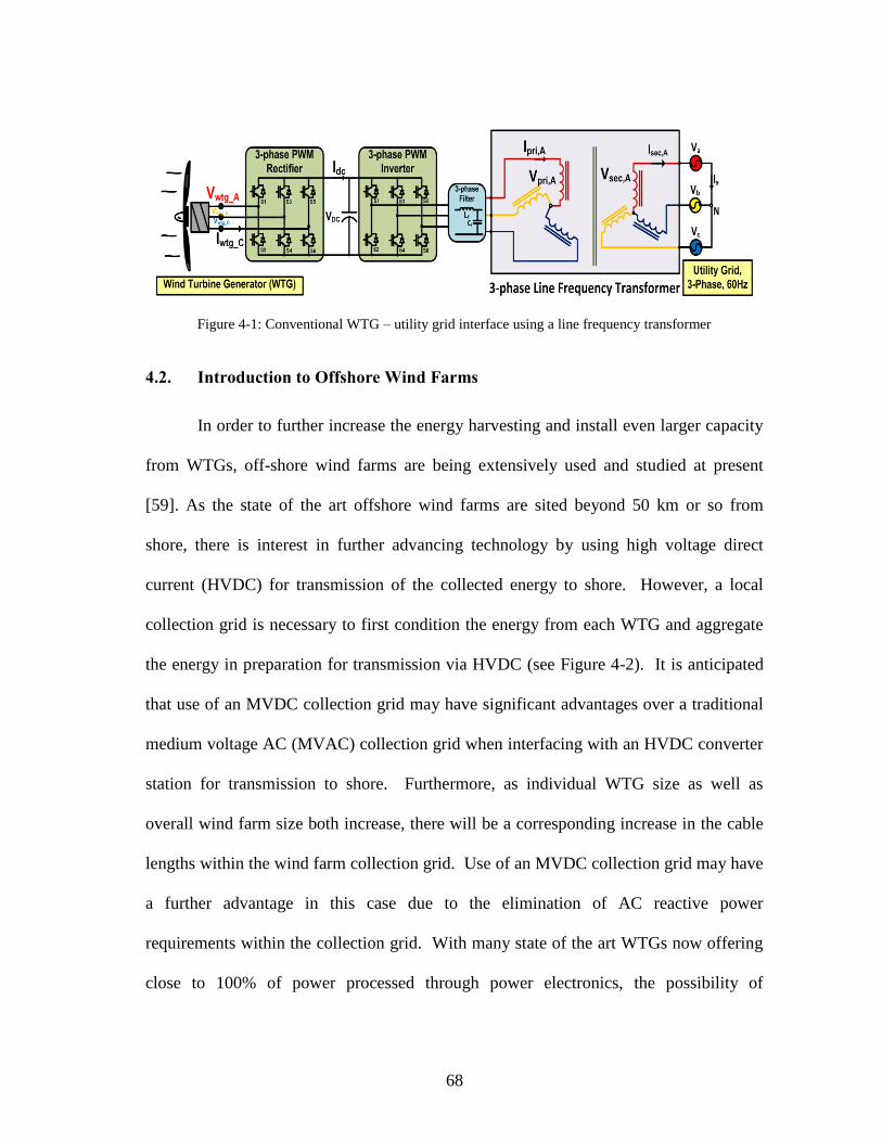
68
Figure 4-1: Conventional WTG – utility grid interface using a line frequency transformer
4.2. Introduction to Offshore Wind Farms
In order to further increase the energy harvesting and install even larger capacity
from WTGs, off-shore wind farms are being extensively used and studied at present
[59]. As the state of the art offshore wind farms are sited beyond 50 km or so from
shore, there is interest in further advancing technology by using high voltage direct
current (HVDC) for transmission of the collected energy to shore. However, a local
collection grid is necessary to first condition the energy from each WTG and aggregate
the energy in preparation for transmission via HVDC (see Figure 4-2). It is anticipated
that use of an MVDC collection grid may have significant advantages over a traditional
medium voltage AC (MVAC) collection grid when interfacing with an HVDC converter
station for transmission to shore. Furthermore, as individual WTG size as well as
overall wind farm size both increase, there will be a corresponding increase in the cable
lengths within the wind farm collection grid. Use of an MVDC collection grid may have
a further advantage in this case due to the elimination of AC reactive power
requirements within the collection grid. With many state of the art WTGs now offering
close to 100% of power processed through power electronics, the possibility of
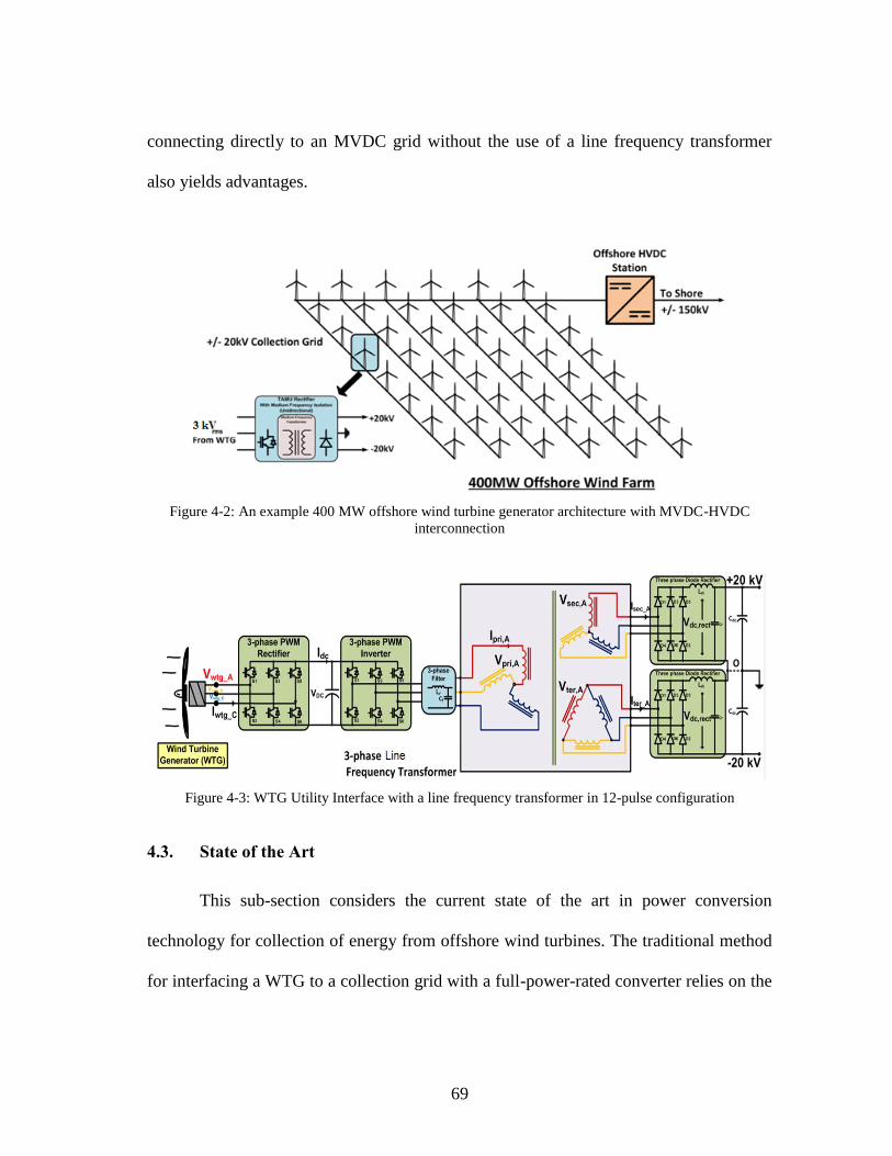
69
connecting directly to an MVDC grid without the use of a line frequency transformer
also yields advantages.
Figure 4-2: An example 400 MW offshore wind turbine generator architecture with MVDC-HVDC
interconnection
Figure 4-3: WTG Utility Interface with a line frequency transformer in 12-pulse configuration
4.3. State of the Art
This sub-section considers the current state of the art in power conversion
technology for collection of energy from offshore wind turbines. The traditional method
for interfacing a WTG to a collection grid with a full-power-rated converter relies on the
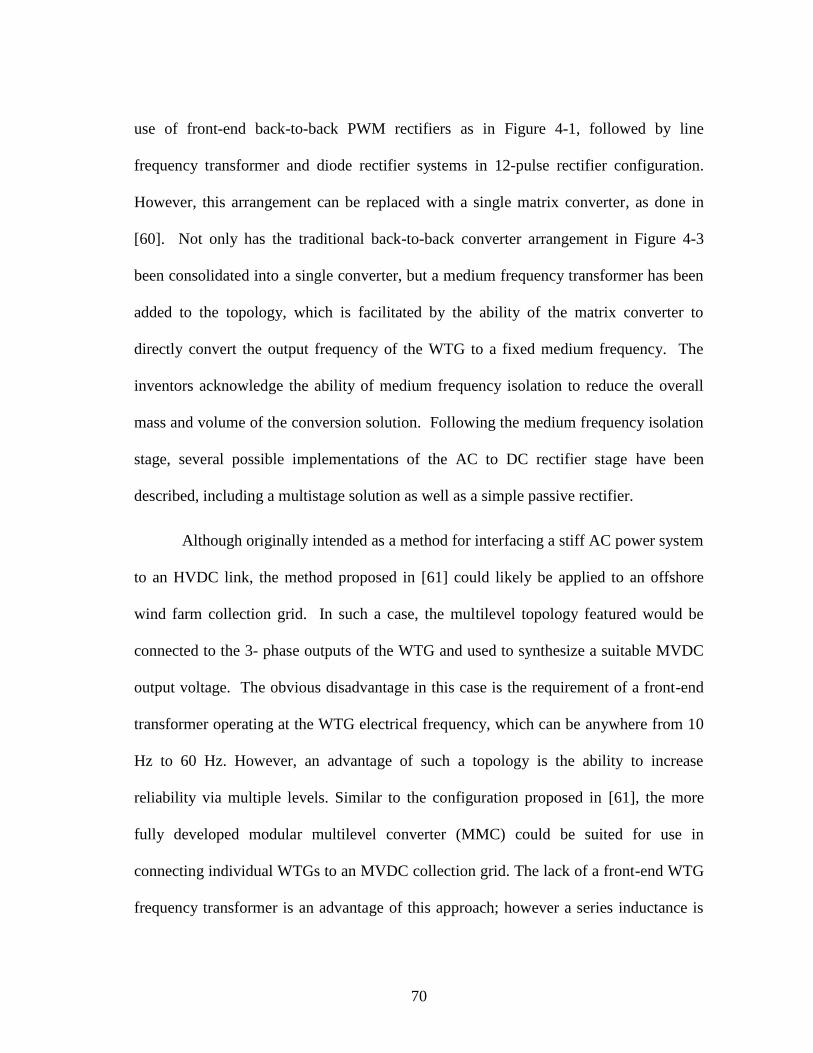
70
use of front-end back-to-back PWM rectifiers as in Figure 4-1, followed by line
frequency transformer and diode rectifier systems in 12-pulse rectifier configuration.
However, this arrangement can be replaced with a single matrix converter, as done in
[60]. Not only has the traditional back-to-back converter arrangement in Figure 4-3
been consolidated into a single converter, but a medium frequency transformer has been
added to the topology, which is facilitated by the ability of the matrix converter to
directly convert the output frequency of the WTG to a fixed medium frequency. The
inventors acknowledge the ability of medium frequency isolation to reduce the overall
mass and volume of the conversion solution. Following the medium frequency isolation
stage, several possible implementations of the AC to DC rectifier stage have been
described, including a multistage solution as well as a simple passive rectifier.
Although originally intended as a method for interfacing a stiff AC power system
to an HVDC link, the method proposed in [61] could likely be applied to an offshore
wind farm collection grid. In such a case, the multilevel topology featured would be
connected to the 3- phase outputs of the WTG and used to synthesize a suitable MVDC
output voltage. The obvious disadvantage in this case is the requirement of a front-end
transformer operating at the WTG electrical frequency, which can be anywhere from 10
Hz to 60 Hz. However, an advantage of such a topology is the ability to increase
reliability via multiple levels. Similar to the configuration proposed in [61], the more
fully developed modular multilevel converter (MMC) could be suited for use in
connecting individual WTGs to an MVDC collection grid. The lack of a front-end WTG
frequency transformer is an advantage of this approach; however a series inductance is
71
still required, although the generator impedance may be sufficient in the case of a
Permanent Magnet Synchronous Generator (PMSG). The lack of isolation between the
WTG and MVDC grid with this approach is a clear disadvantage, especially in a large
wind farm. Also, capacitor charge balancing becomes difficult for many levels.
The approach proposed in [62] provides a simple and effective way to interface
the WTG to an MVDC grid, although there are a few unique disadvantages as well. The
use of MF isolation is desirable and significantly reduces system mass and volume;
however, this approach assumes the WTG to have an operating frequency of 1.2 kHz,
requiring a large number of poles which results in a larger diameter machine. The
secondary side of the MF transformer is tied to the MVDC grid via a passive diode
rectifier, which is simple and reliable, but is unidirectional and requires a secondary
power converter to supply reactive power to the WTG. It may introduce significant
harmonics. Furthermore, there is no obvious strategy for controlling the MVDC
collection grid voltage. Some other topologies have also been published in the literature,
which can be adapted to a WTG-MVDC interconnection [11, 13]
This section investigates a new approach to the conversion and collection of
energy from offshore wind turbine generators (WTGs) and the interconnection between
individual WTGs and a medium voltage DC (MVDC) collection grid. Several candidate
converter topologies and MVDC collection grid architectures were investigated
throughout this work, including series/parallel connection of WTGs, as well as various
MVDC collection grid voltages. Following the investigation of various MVDC
collection grid architectures, a voltage of +/- 20 kV was arrived at for the MVDC. The
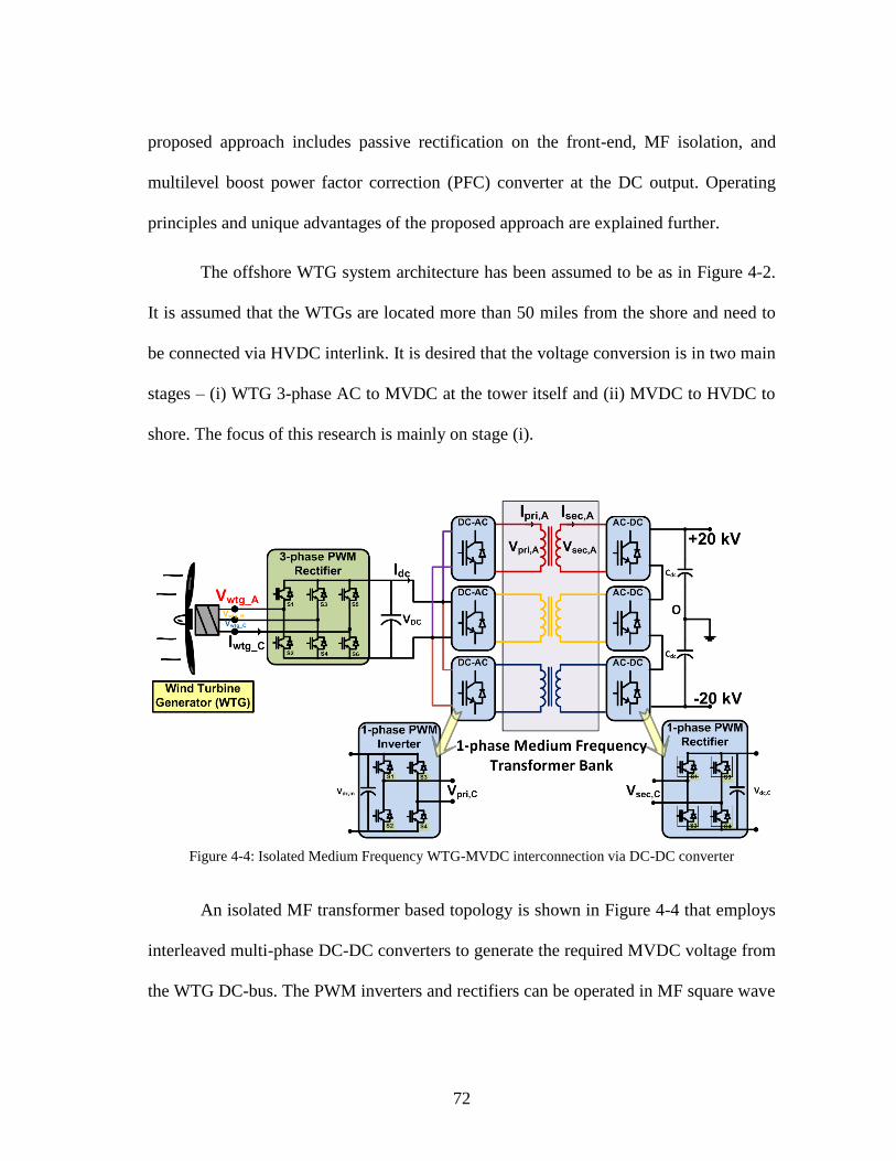
72
proposed approach includes passive rectification on the front-end, MF isolation, and
multilevel boost power factor correction (PFC) converter at the DC output. Operating
principles and unique advantages of the proposed approach are explained further.
The offshore WTG system architecture has been assumed to be as in Figure 4-2.
It is assumed that the WTGs are located more than 50 miles from the shore and need to
be connected via HVDC interlink. It is desired that the voltage conversion is in two main
stages – (i) WTG 3-phase AC to MVDC at the tower itself and (ii) MVDC to HVDC to
shore. The focus of this research is mainly on stage (i).
Figure 4-4: Isolated Medium Frequency WTG-MVDC interconnection via DC-DC converter
An isolated MF transformer based topology is shown in Figure 4-4 that employs
interleaved multi-phase DC-DC converters to generate the required MVDC voltage from
the WTG DC-bus. The PWM inverters and rectifiers can be operated in MF square wave
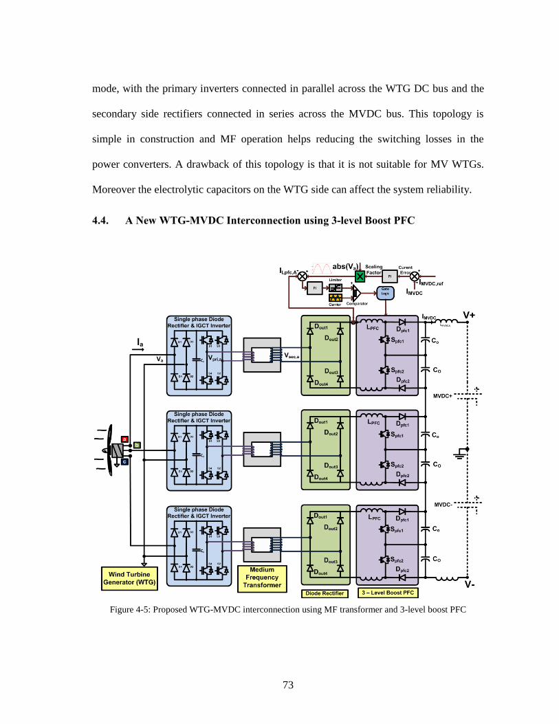
73
mode, with the primary inverters connected in parallel across the WTG DC bus and the
secondary side rectifiers connected in series across the MVDC bus. This topology is
simple in construction and MF operation helps reducing the switching losses in the
power converters. A drawback of this topology is that it is not suitable for MV WTGs.
Moreover the electrolytic capacitors on the WTG side can affect the system reliability.
4.4. A New WTG-MVDC Interconnection using 3-level Boost PFC
Figure 4-5: Proposed WTG-MVDC interconnection using MF transformer and 3-level boost PFC
74
The proposed topology is illustrated in Figure 4-5. This topology is derived from
the concept proposed in Figure 2-4 under section 2.2. The major differences are that 3-
level boost PFCs are used here instead of simple PFCs and the output DC voltages are
connected in series instead of parallel. Moreover the presence of large input inductances
in synchronous WTGs causes EMI challenges, especially with diode front-end. The
design can be broadly divided into the following main sub-sections: AC-AC converter,
1-phase boost PFCs, control strategy, filter design and MF transformer.
4.4.1. AC-AC Converter
There are three 1-phase AC-AC converters in the proposed approach, similar to
the ones described in earlier sections. Here too, the converters can be constructed using
AC-AC H-bridge using bidirectional switches. Each AC-AC converter consists of a 1-
phase diode bridge and a 1-phase inverter H-bridge (with IGCTs) connected by de-
coupling capacitors. In order to interface to a 3.0 kVLL(max), fs = 60 Hz(max) 3-phase wind
turbine generator (WTG), 5.5 kV rated diodes and IGCTs will be sufficient or series
stacked lower voltage devices can be used. The AC-AC converter switching functions
are given by (2.1), (2.2) and (2.3) from section 2.2.1. Even if the frequency of WTG AC
varies, the transformer operating frequency does not change much. This property can
make the proposed topology attractive for wind turbine and adjustable speed drive
applications where the operating frequency varies.
4.4.2. Single Phase 3-level Boost PFCs
The transformer secondary voltage is a ‘flipped sine wave’ (product of line
frequency sine and MF square wave, slightly smoothened due to the filtering action of
75
the transformer leakage inductance. The diode rectifier of the boost PFC stage converts
this flipped sine wave into full-wave rectified (twice-the-WTG-frequency) waveform. It
should be noted that even though the transformer frequency is HF or MF, the diode
rectifier switches at that frequency and the rectified voltage on the transformer
secondary looks similar to the rectified voltage waveform of the weak DC-link on the
primary (WTG) side. After this, the remaining boost converter in the PFC operates like a
conventional 3-level PFC, making the inductor current in phase/shape as the rectified
voltage [13, 14, 63, 64]. Thus, the design of this topology is straight forward. Since the
transformer leakage inductance filters the high frequency components in the voltage, a
small capacitor has to be plugged-in across the secondary to suppress transient voltages.
If ‘β’ is the minimum boost PFC gain (~ 1.5 to 2.0). If Vdc is the required DC
output voltage, the required transformer turns-ration, N can be calculated as per (4.1):
𝑁 =𝑛2
𝑛1= (
𝜋
2√2∙𝛽) ∙ (
𝑉𝐷𝐶
𝑉𝑎(𝑟𝑚𝑠))
For a 3 kVLL WTG input, MVDC voltage of 14 kVdc per phase (~2*20/3 kV) and
for a β value of 1.5, the transformer turns ratio is approximately n2:n1 = 6:1. Higher
turns-ration in a MF transformer or HF transformer can cause significant corona losses
that affect size advantage. Boost PFC [64] switches have to be rated (after 50% derating)
at nearly 30 kV, that amounts to nearly six IGCTs in series. While the current rating of
the primary side converters is nearly 2000 A(pk), the secondary side converters have to be
rated (with 30% derating) at nearly 400 A(pk).
(4.1)
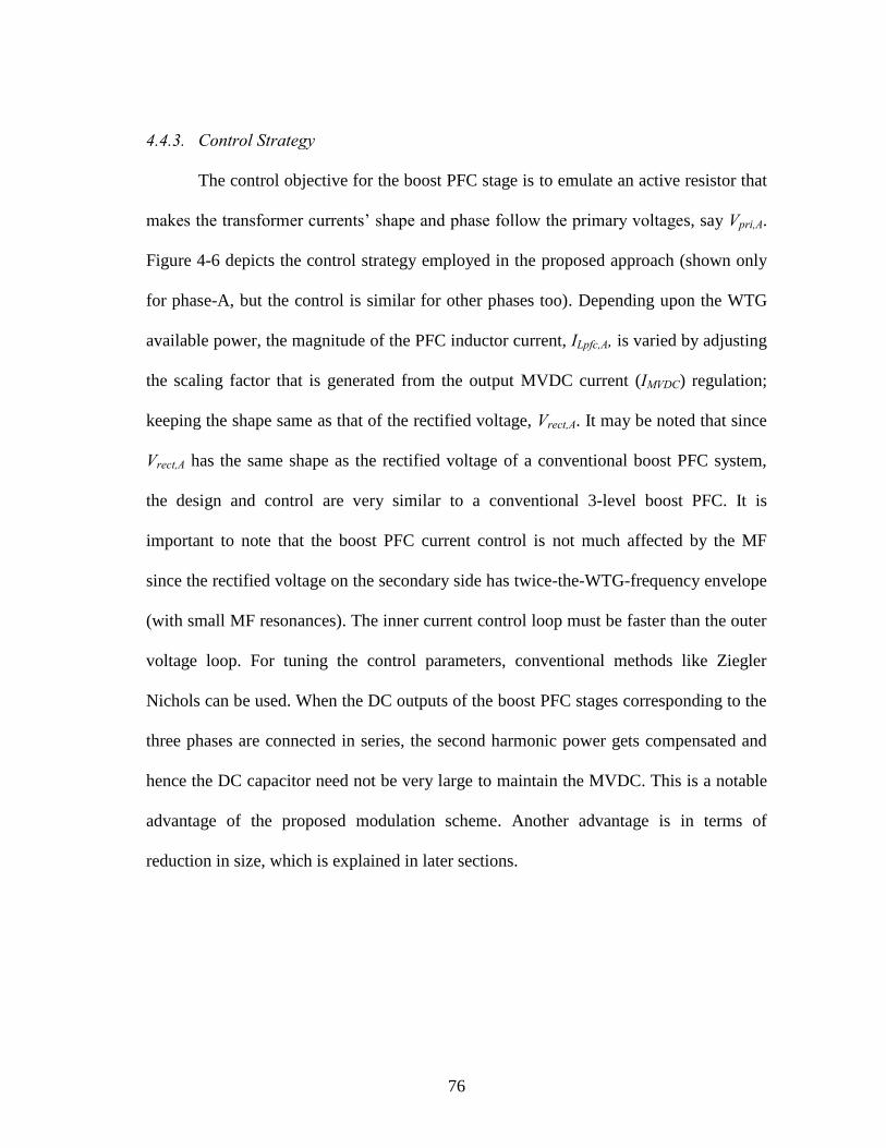
76
4.4.3. Control Strategy
The control objective for the boost PFC stage is to emulate an active resistor that
makes the transformer currents’ shape and phase follow the primary voltages, say Vpri,A.
Figure 4-6 depicts the control strategy employed in the proposed approach (shown only
for phase-A, but the control is similar for other phases too). Depending upon the WTG
available power, the magnitude of the PFC inductor current, ILpfc,A, is varied by adjusting
the scaling factor that is generated from the output MVDC current (IMVDC) regulation;
keeping the shape same as that of the rectified voltage, Vrect,A. It may be noted that since
Vrect,A has the same shape as the rectified voltage of a conventional boost PFC system,
the design and control are very similar to a conventional 3-level boost PFC. It is
important to note that the boost PFC current control is not much affected by the MF
since the rectified voltage on the secondary side has twice-the-WTG-frequency envelope
(with small MF resonances). The inner current control loop must be faster than the outer
voltage loop. For tuning the control parameters, conventional methods like Ziegler
Nichols can be used. When the DC outputs of the boost PFC stages corresponding to the
three phases are connected in series, the second harmonic power gets compensated and
hence the DC capacitor need not be very large to maintain the MVDC. This is a notable
advantage of the proposed modulation scheme. Another advantage is in terms of
reduction in size, which is explained in later sections.
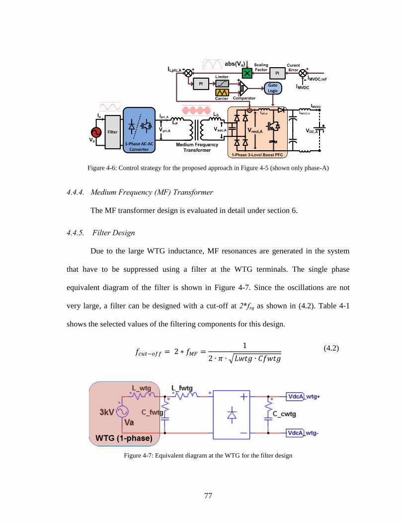
77
Figure 4-6: Control strategy for the proposed approach in Figure 4-5 (shown only phase-A)
4.4.4. Medium Frequency (MF) Transformer
The MF transformer design is evaluated in detail under section 6.
4.4.5. Filter Design
Due to the large WTG inductance, MF resonances are generated in the system
that have to be suppressed using a filter at the WTG terminals. The single phase
equivalent diagram of the filter is shown in Figure 4-7. Since the oscillations are not
very large, a filter can be designed with a cut-off at 2*fsq as shown in (4.2). Table 4-1
shows the selected values of the filtering components for this design.
𝑓𝑐𝑢𝑡−𝑜𝑓𝑓 = 2 ∗ 𝑓𝑀𝐹 =1
2 ∙ 𝜋 ∙ √𝐿𝑤𝑡𝑔 ∙ 𝐶𝑓𝑤𝑡𝑔
Figure 4-7: Equivalent diagram at the WTG for the filter design
(4.2)
78
Table 4-1: Filter design parameters and values
Parameters Values
Generator Voltage (Va) 3 kV
rms(LL) to 1.5 kV
rms(LL)
Generator Frequency 60 Hz to 30 Hz
Inverter Frequency (fMF
) 600 Hz
Generator Impedance (Lwtg
) 4 mH (1.0 p.u. per phase), 10mOhms
Input filter Capacitor (Cfwtg
) 10 uF
Input filter Inductor (Lfwtg
) 10.0 uH
WTG DC Bus Capacitor (Ccwtg
) 1.0 uF
4.5. Maximum Power Point Tracking (MPPT)
The direct-drive PMSG based WTGs typically follow the curves mentioned in
Figure 4-8 [65]. At low wind speeds, the turbine is operated at maximum aerodynamic
efficiency up to the rated rotor speed of around 14 RPM (for an 8 MVA machine); at
high wind speeds, the pitch control keeps the rotor speed at 14 rpm. For any wind
velocity, there is a particular WTG speed at which the power generated is maximized.
The equations mentioned in [66] can be modeled in a block with wind velocity as input
and used to generate the reference speed and voltage at a particular wind speed. There
are three main MPPT methods used (shown in [66]). In this topology, the power signal
feedback (PSF) algorithm can be used along with the Hill-Climb Search (HCS)
algorithm in such a way that the fast convergence of the former and precision of the
latter can be clubbed. Salient features of both the algorithms are explained through [66].
PSF algorithm requires the knowledge of the WTG’s MPP curve and tracks this
curve through its control mechanisms. The maximum power curves need to be obtained
via simulations or off-line experiment on individual wind turbines. Reference power is
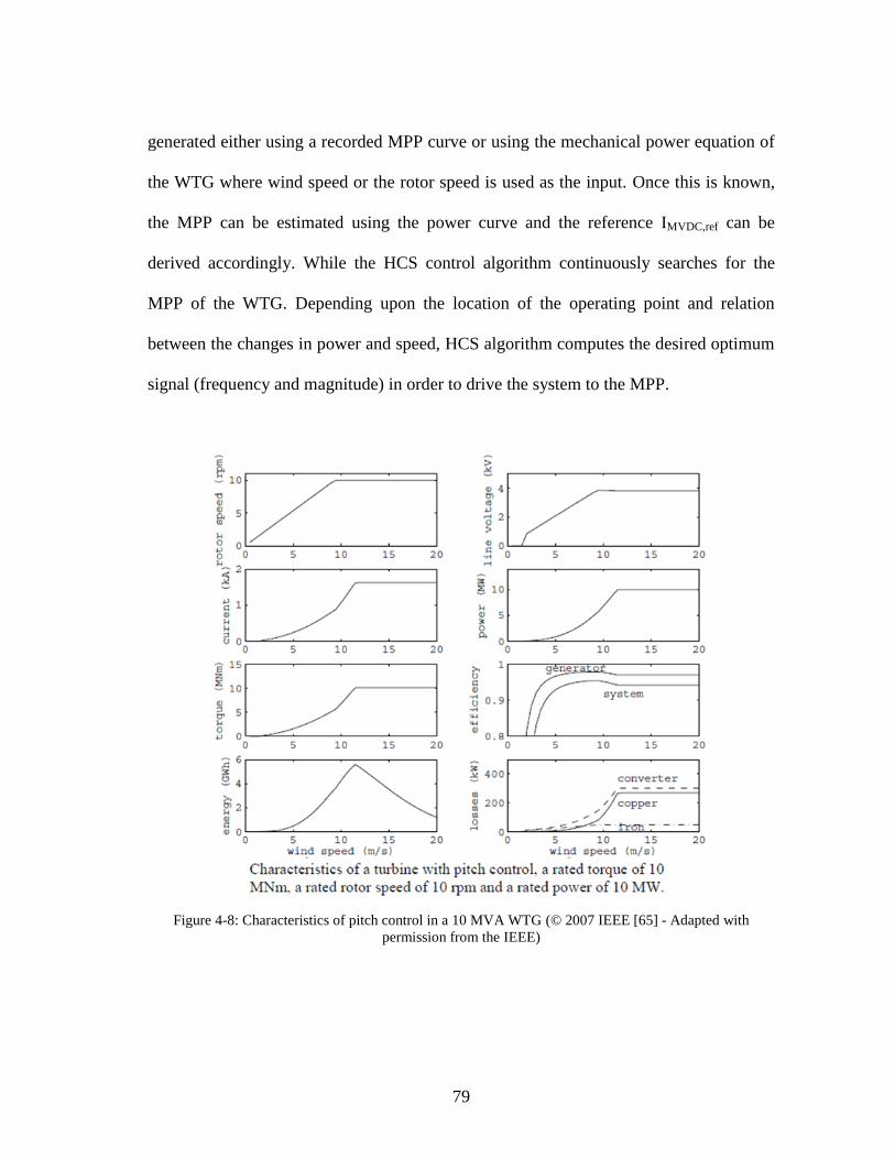
79
generated either using a recorded MPP curve or using the mechanical power equation of
the WTG where wind speed or the rotor speed is used as the input. Once this is known,
the MPP can be estimated using the power curve and the reference IMVDC,ref can be
derived accordingly. While the HCS control algorithm continuously searches for the
MPP of the WTG. Depending upon the location of the operating point and relation
between the changes in power and speed, HCS algorithm computes the desired optimum
signal (frequency and magnitude) in order to drive the system to the MPP.
Figure 4-8: Characteristics of pitch control in a 10 MVA WTG (© 2007 IEEE [65] - Adapted with
permission from the IEEE)
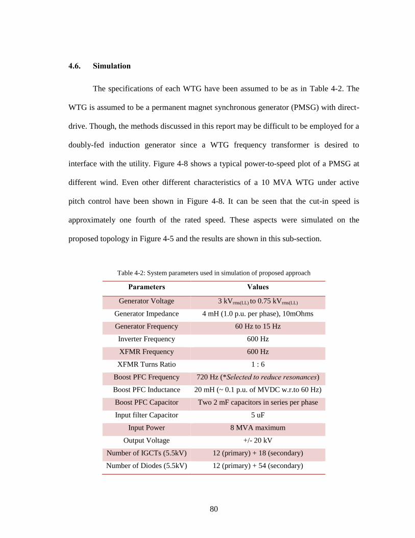
80
4.6. Simulation
The specifications of each WTG have been assumed to be as in Table 4-2. The
WTG is assumed to be a permanent magnet synchronous generator (PMSG) with direct-
drive. Though, the methods discussed in this report may be difficult to be employed for a
doubly-fed induction generator since a WTG frequency transformer is desired to
interface with the utility. Figure 4-8 shows a typical power-to-speed plot of a PMSG at
different wind. Even other different characteristics of a 10 MVA WTG under active
pitch control have been shown in Figure 4-8. It can be seen that the cut-in speed is
approximately one fourth of the rated speed. These aspects were simulated on the
proposed topology in Figure 4-5 and the results are shown in this sub-section.
Table 4-2: System parameters used in simulation of proposed approach
Parameters Values
Generator Voltage 3 kVrms(LL) to 0.75 kVrms(LL)
Generator Impedance 4 mH (1.0 p.u. per phase), 10mOhms
Generator Frequency 60 Hz to 15 Hz
Inverter Frequency 600 Hz
XFMR Frequency 600 Hz
XFMR Turns Ratio 1 : 6
Boost PFC Frequency 720 Hz (*Selected to reduce resonances)
Boost PFC Inductance 20 mH (~ 0.1 p.u. of MVDC w.r.to 60 Hz)
Boost PFC Capacitor Two 2 mF capacitors in series per phase
Input filter Capacitor 5 uF
Input Power 8 MVA maximum
Output Voltage +/- 20 kV
Number of IGCTs (5.5kV) 12 (primary) + 18 (secondary)
Number of Diodes (5.5kV) 12 (primary) + 54 (secondary)
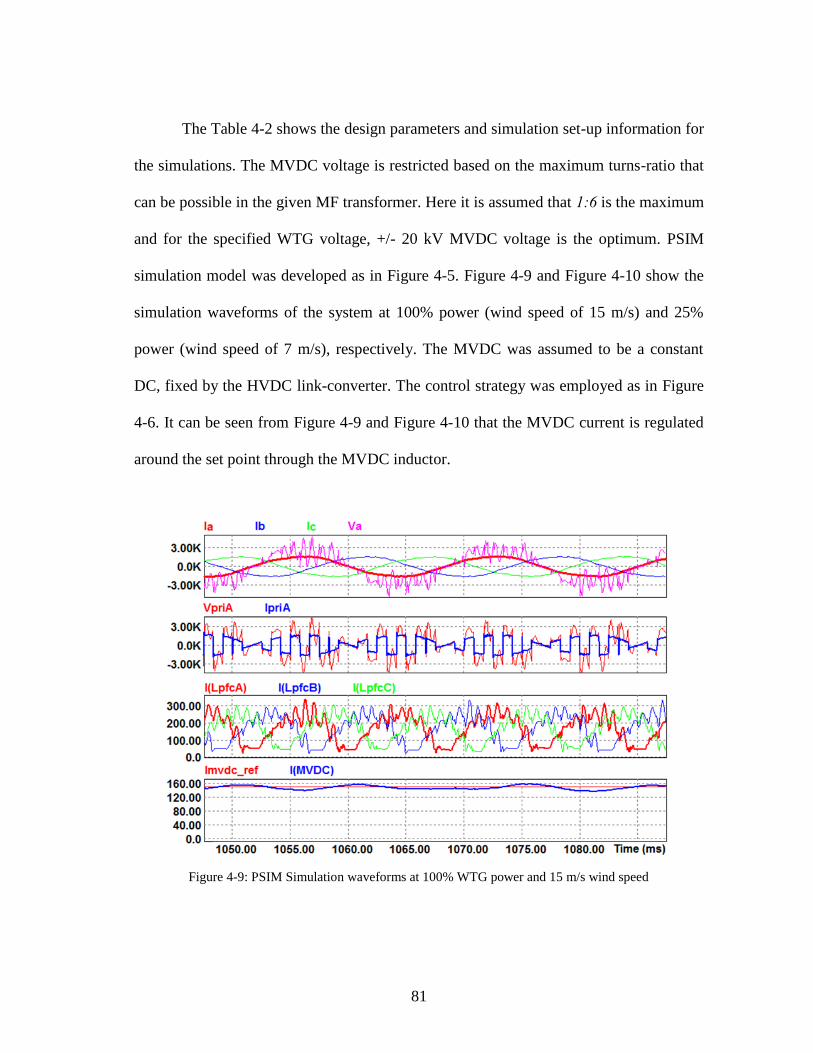
81
The Table 4-2 shows the design parameters and simulation set-up information for
the simulations. The MVDC voltage is restricted based on the maximum turns-ratio that
can be possible in the given MF transformer. Here it is assumed that 1:6 is the maximum
and for the specified WTG voltage, +/- 20 kV MVDC voltage is the optimum. PSIM
simulation model was developed as in Figure 4-5. Figure 4-9 and Figure 4-10 show the
simulation waveforms of the system at 100% power (wind speed of 15 m/s) and 25%
power (wind speed of 7 m/s), respectively. The MVDC was assumed to be a constant
DC, fixed by the HVDC link-converter. The control strategy was employed as in Figure
4-6. It can be seen from Figure 4-9 and Figure 4-10 that the MVDC current is regulated
around the set point through the MVDC inductor.
Figure 4-9: PSIM Simulation waveforms at 100% WTG power and 15 m/s wind speed
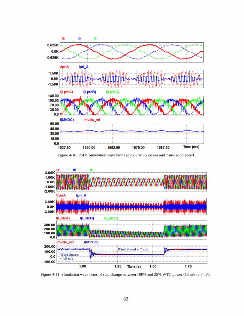
82
Figure 4-10: PSIM Simulation waveforms at 25% WTG power and 7 m/s wind speed
Figure 4-11: Simulation waveforms of step change between 100% and 25% WTG power (15 m/s to 7 m/s)
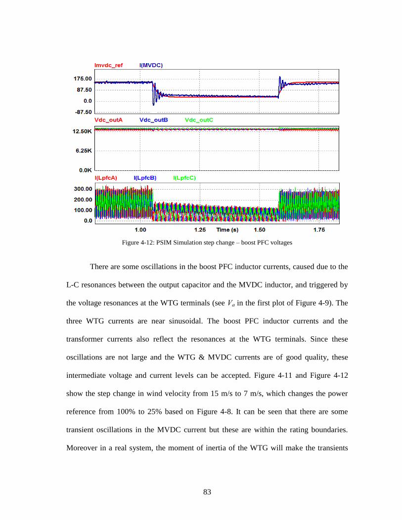
83
Figure 4-12: PSIM Simulation step change – boost PFC voltages
There are some oscillations in the boost PFC inductor currents, caused due to the
L-C resonances between the output capacitor and the MVDC inductor, and triggered by
the voltage resonances at the WTG terminals (see Va in the first plot of Figure 4-9). The
three WTG currents are near sinusoidal. The boost PFC inductor currents and the
transformer currents also reflect the resonances at the WTG terminals. Since these
oscillations are not large and the WTG & MVDC currents are of good quality, these
intermediate voltage and current levels can be accepted. Figure 4-11 and Figure 4-12
show the step change in wind velocity from 15 m/s to 7 m/s, which changes the power
reference from 100% to 25% based on Figure 4-8. It can be seen that there are some
transient oscillations in the MVDC current but these are within the rating boundaries.
Moreover in a real system, the moment of inertia of the WTG will make the transients
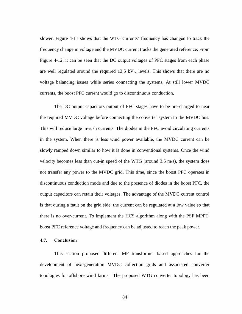
84
slower. Figure 4-11 shows that the WTG currents’ frequency has changed to track the
frequency change in voltage and the MVDC current tracks the generated reference. From
Figure 4-12, it can be seen that the DC output voltages of PFC stages from each phase
are well regulated around the required 13.5 kVdc levels. This shows that there are no
voltage balancing issues while series connecting the systems. At still lower MVDC
currents, the boost PFC current would go to discontinuous conduction.
The DC output capacitors output of PFC stages have to be pre-charged to near
the required MVDC voltage before connecting the converter system to the MVDC bus.
This will reduce large in-rush currents. The diodes in the PFC avoid circulating currents
in the system. When there is less wind power available, the MVDC current can be
slowly ramped down similar to how it is done in conventional systems. Once the wind
velocity becomes less than cut-in speed of the WTG (around 3.5 m/s), the system does
not transfer any power to the MVDC grid. This time, since the boost PFC operates in
discontinuous conduction mode and due to the presence of diodes in the boost PFC, the
output capacitors can retain their voltages. The advantage of the MVDC current control
is that during a fault on the grid side, the current can be regulated at a low value so that
there is no over-current. To implement the HCS algorithm along with the PSF MPPT,
boost PFC reference voltage and frequency can be adjusted to reach the peak power.
4.7. Conclusion
This section proposed different MF transformer based approaches for the
development of next-generation MVDC collection grids and associated converter
topologies for offshore wind farms. The proposed WTG converter topology has been

85
shown to be suitable over a conventional approach for interfacing WTGs to an MVDC
collection grid of +/- 20 kV in terms of mass and volume, which is anticipated to reduce
the overall cost of delivering energy from offshore wind farms to shore. Different
operating modes of the proposed approach have been analyzed and the proposed
converter topology has been shown to be feasible with current state-of-the-art power
semiconductor technology and transformer materials. The simulation results provided
initial proof for the concepts and it could be seen that the control can support the typical
WTG features such as MPPT, fault regulation, soft-start, etc.
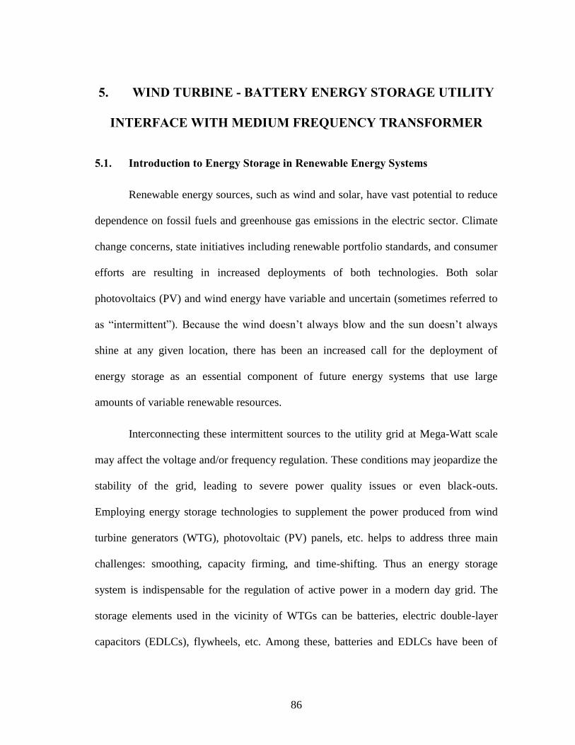
86
5. WIND TURBINE - BATTERY ENERGY STORAGE UTILITY
INTERFACE WITH MEDIUM FREQUENCY TRANSFORMER
5.1. Introduction to Energy Storage in Renewable Energy Systems
Renewable energy sources, such as wind and solar, have vast potential to reduce
dependence on fossil fuels and greenhouse gas emissions in the electric sector. Climate
change concerns, state initiatives including renewable portfolio standards, and consumer
efforts are resulting in increased deployments of both technologies. Both solar
photovoltaics (PV) and wind energy have variable and uncertain (sometimes referred to
as “intermittent”). Because the wind doesn’t always blow and the sun doesn’t always
shine at any given location, there has been an increased call for the deployment of
energy storage as an essential component of future energy systems that use large
amounts of variable renewable resources.
Interconnecting these intermittent sources to the utility grid at Mega-Watt scale
may affect the voltage and/or frequency regulation. These conditions may jeopardize the
stability of the grid, leading to severe power quality issues or even black-outs.
Employing energy storage technologies to supplement the power produced from wind
turbine generators (WTG), photovoltaic (PV) panels, etc. helps to address three main
challenges: smoothing, capacity firming, and time-shifting. Thus an energy storage
system is indispensable for the regulation of active power in a modern day grid. The
storage elements used in the vicinity of WTGs can be batteries, electric double-layer
capacitors (EDLCs), flywheels, etc. Among these, batteries and EDLCs have been of
87
major focus in the power electronics industry. However, their interface to the utility grid
is challenging, especially in the medium voltage (MV) scale [67-70] WTGs can operate
at maximum power coefficient over a wide range of wind speeds if operated in a variable
speed mode [70]. Permanent Magnet (PM) WTGs are becoming more prominent for
high power energy conversion mainly because of high power density and flexibility in
operation. Direct drive power conversion scheme is popularly used for PM WTGs.
Several approaches have been reported in the literature to interface battery
energy storage systems (BESS) with the utility [43, 71-73]. Figure 5-1 shows the
conventional approach employing a line frequency transformer to charge/discharge a
low voltage battery energy storage bank [71]. This approach requires a line frequency
step-up transformer in order to be connected to a medium voltage grid. Figure 5-2 shows
a PWM rectifier followed by a high frequency link DC-DC converter interfaced to a
battery bank. This approach may not be suitable for MV utility interface, due to the
presence of the simple 3-phase inverter. NPC inverters can be used if interfacing with a
higher utility voltage is desired.
Figure 5-1: Medium voltage (or low voltage) utility - energy storage interface topology with line
frequency transformer and PWM Rectifier
88
Figure 5-2: Lower voltage utility - energy storage interface topology involving high frequency transformer
and two converter stages [73]
Reference [73] illustrates cascaded H-bridge based PWM rectifiers interfaced via
a line frequency transformer. This approach requires several battery banks to be arranged
in groups, thus requiring multiple charge balance approaches. A 10-MW, 40-MWh
battery energy storage system has been described in the literature [74], that combines an
18-pulse voltage-source converter with lead-acid batteries where the dc voltage ranged
from 1750 to 2860 V. Another concept with a 5-MVA 2.5-MWh battery energy storage
system with lead-acid batteries based on parallel operation of 12-pulse converters to
achieve the required power rating described in [72]. A common disadvantage with the
above described approaches is the presence of bulky line frequency 50/60 Hz
transformer in addition to complexity in control.
Many topologies to interface BESS with WTG systems have also been proposed
and/or evaluated [75, 76]. Most of them propose different ways of integrating the BESS
to the WTG system DC link, while other alternatives are interfacing the two systems at
the utility side using separate line frequency transformers. The former method is good
for lower power interface, but interfacing the two systems at the DC link at high power
requires the use of transformers. The latter method also requires two separate bulky line
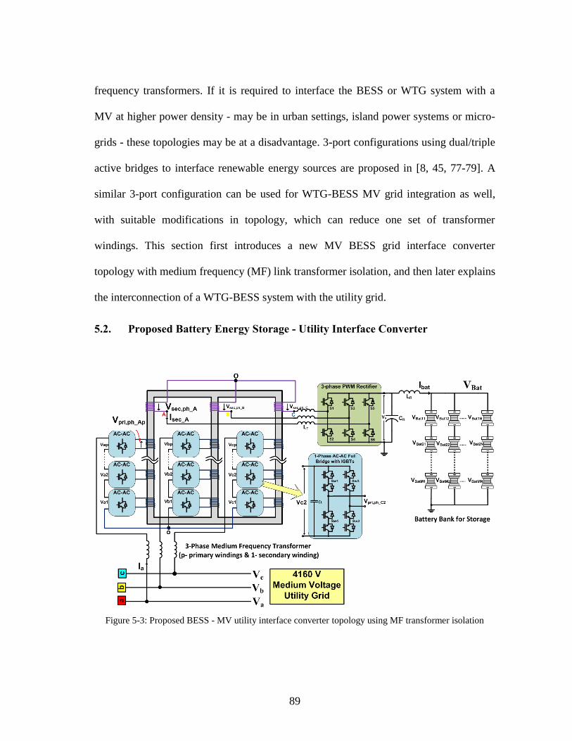
89
frequency transformers. If it is required to interface the BESS or WTG system with a
MV at higher power density - may be in urban settings, island power systems or micro-
grids - these topologies may be at a disadvantage. 3-port configurations using dual/triple
active bridges to interface renewable energy sources are proposed in [8, 45, 77-79]. A
similar 3-port configuration can be used for WTG-BESS MV grid integration as well,
with suitable modifications in topology, which can reduce one set of transformer
windings. This section first introduces a new MV BESS grid interface converter
topology with medium frequency (MF) link transformer isolation, and then later explains
the interconnection of a WTG-BESS system with the utility grid.
5.2. Proposed Battery Energy Storage - Utility Interface Converter
Figure 5-3: Proposed BESS - MV utility interface converter topology using MF transformer isolation
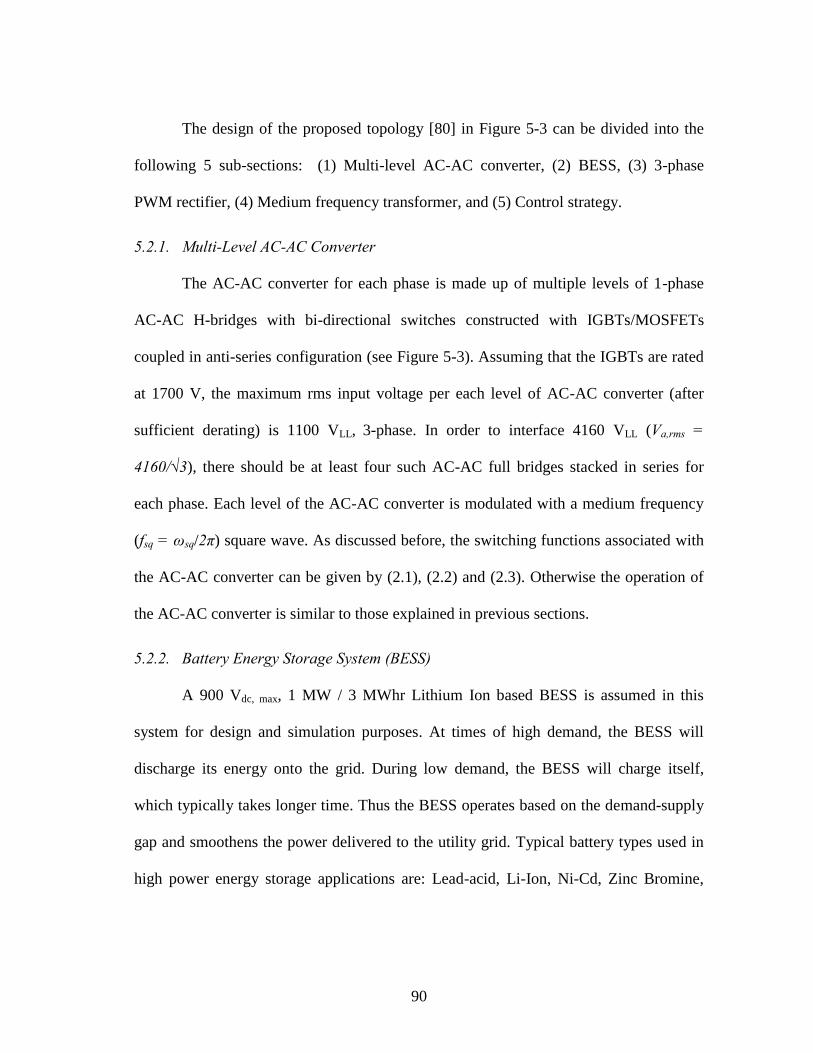
90
The design of the proposed topology [80] in Figure 5-3 can be divided into the
following 5 sub-sections: (1) Multi-level AC-AC converter, (2) BESS, (3) 3-phase
PWM rectifier, (4) Medium frequency transformer, and (5) Control strategy.
5.2.1. Multi-Level AC-AC Converter
The AC-AC converter for each phase is made up of multiple levels of 1-phase
AC-AC H-bridges with bi-directional switches constructed with IGBTs/MOSFETs
coupled in anti-series configuration (see Figure 5-3). Assuming that the IGBTs are rated
at 1700 V, the maximum rms input voltage per each level of AC-AC converter (after
sufficient derating) is 1100 VLL, 3-phase. In order to interface 4160 VLL (Va,rms =
4160/√3), there should be at least four such AC-AC full bridges stacked in series for
each phase. Each level of the AC-AC converter is modulated with a medium frequency
(fsq = ωsq/2π) square wave. As discussed before, the switching functions associated with
the AC-AC converter can be given by (2.1), (2.2) and (2.3). Otherwise the operation of
the AC-AC converter is similar to those explained in previous sections.
5.2.2. Battery Energy Storage System (BESS)
A 900 Vdc, max, 1 MW / 3 MWhr Lithium Ion based BESS is assumed in this
system for design and simulation purposes. At times of high demand, the BESS will
discharge its energy onto the grid. During low demand, the BESS will charge itself,
which typically takes longer time. Thus the BESS operates based on the demand-supply
gap and smoothens the power delivered to the utility grid. Typical battery types used in
high power energy storage applications are: Lead-acid, Li-Ion, Ni-Cd, Zinc Bromine,
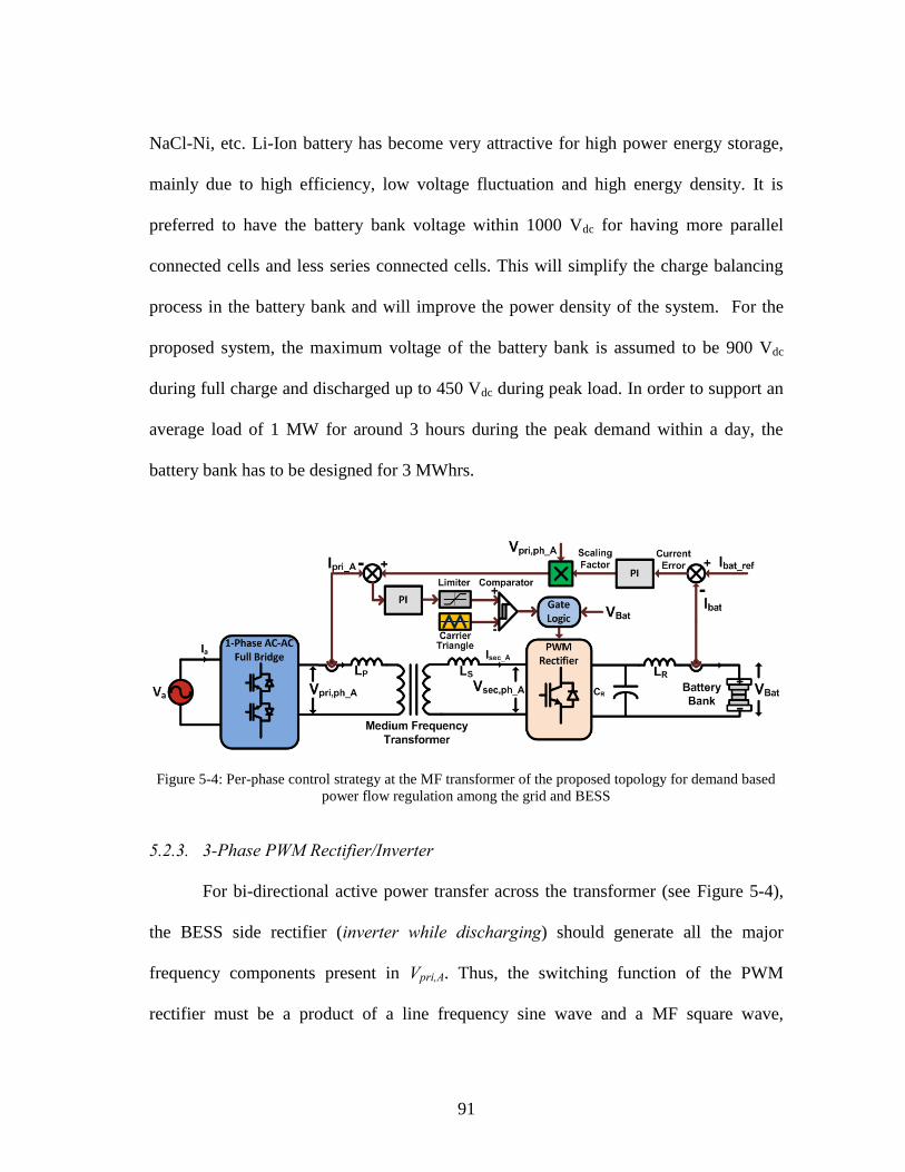
91
NaCl-Ni, etc. Li-Ion battery has become very attractive for high power energy storage,
mainly due to high efficiency, low voltage fluctuation and high energy density. It is
preferred to have the battery bank voltage within 1000 Vdc for having more parallel
connected cells and less series connected cells. This will simplify the charge balancing
process in the battery bank and will improve the power density of the system. For the
proposed system, the maximum voltage of the battery bank is assumed to be 900 Vdc
during full charge and discharged up to 450 Vdc during peak load. In order to support an
average load of 1 MW for around 3 hours during the peak demand within a day, the
battery bank has to be designed for 3 MWhrs.
Figure 5-4: Per-phase control strategy at the MF transformer of the proposed topology for demand based
power flow regulation among the grid and BESS
5.2.3. 3-Phase PWM Rectifier/Inverter
For bi-directional active power transfer across the transformer (see Figure 5-4),
the BESS side rectifier (inverter while discharging) should generate all the major
frequency components present in Vpri,A. Thus, the switching function of the PWM
rectifier must be a product of a line frequency sine wave and a MF square wave,

92
(5.1)
appropriately phase-shifted depending on the amount of power to be transferred
(achieved by PI control of transformer phase currents by forcing the currents’ shapes to
be similar to transformer primary voltages). The transformer leakage inductances act as
the power transferring reactors. Considering the peak BESS voltage as 900 Vdc, 1700 V
IGBTs can be employed to attain around 1000 Apk current rating for a system power of 1
MW. The per phase active power (Pa1) transferred to the utility side at a single level
across the transformer from the BESS can be given by (5.1) and (5.2).
𝑃𝑎1 = 𝐾 ∙ ∑ {V𝑝𝑟𝑖𝐴
(𝑓)∙ V𝑠𝑒𝑐,𝑤𝑡𝑔_𝐴
(𝑓)∙ [
sin𝛿(𝑓)
𝑓]}
𝑓=∞
𝑓=(𝑓𝑠𝑞+𝑓𝑠),
(𝑓𝑠𝑞−𝑓𝑠),
(3.𝑓𝑠𝑞+𝑓𝑠),…
K = (𝑛1∙𝑛2
2∙𝜋∙(𝑛22∙𝐿𝑝+𝑛1
2∙𝐿𝑠))
where n1, n2 are the number of transformer primary and secondary turns, respectively; Lp,
Ls are the transformer primary and secondary leakage inductances (assuming that the
transformer winding resistances are small); Vpri_A(f)
and Vsec,wtg_A(f)
are respectively the
primary and secondary transformer phase voltage (rms) components in the frequency
spectrum with a frequency of ‘f’; and δ(f) is the phase difference across the transformer
primary and secondary voltage components with frequency, f.
5.2.4. Medium Frequency (MF) Transformer
Medium frequency (MF) transformer design is again similar as in previous
sections, and will be detailed in section 6. Based on the AC-AC converter and PWM
rectifier operations, the minimum transformer turns ratio can be calculated by (5.3):
(5.2)
93
𝑁 =n2
n1= (
1
2√2) ∙ (
VBat(min)
Va(rms))
For a 4160VLL utility input, and at 450Vdc minimum battery voltage, the
transformer turns ratio required is n2:n1 = 1:15 (considering the primary windings across
all levels). If the battery voltage variation is reduced, the turns-ratio can be increased.
5.2.5. Control Strategy
The detailed control strategy adopted for the proposed system (see Figure 5-3)
can be seen in Figure 5-4 (only one transformer phase is shown for simplicity, but it also
applies for other transformer phases of the proposed topology) for controlling the
charging/discharging of BESS. The control mainly consists of two current loops – (a) the
external loop regulating the DC current, Ibat, with a bandwidth of close to 100 Hz or
below (as per the system speed requirement) and (b) the internal loop regulating the
transformer current, Ipri,A, with a bandwidth of at least five times the MF (here, 3-4 kHz);
which is due to exactly replicate the transformer voltage shape to the current as well,
where up to 5th
frequency component are essential. There will be two more such internal
loops for the other transformer phase currents. The outer loop is common for all the
inner loops and will typically be slower than the inner loops.
On the utility side, the input capacitors and the multiple windings in the
transformer will assure the voltage to be distributed evenly across the windings. As the
AC-AC converter is modulated with a square wave, the transformer windings experience
such a ‘multiple-frequency’ voltage waveform. The controller senses these voltages for
uniformity and evaluates the grid demand to calculate how much current must flow at
any time. This information is used to control the BESS DC current by switching the
(5.3)
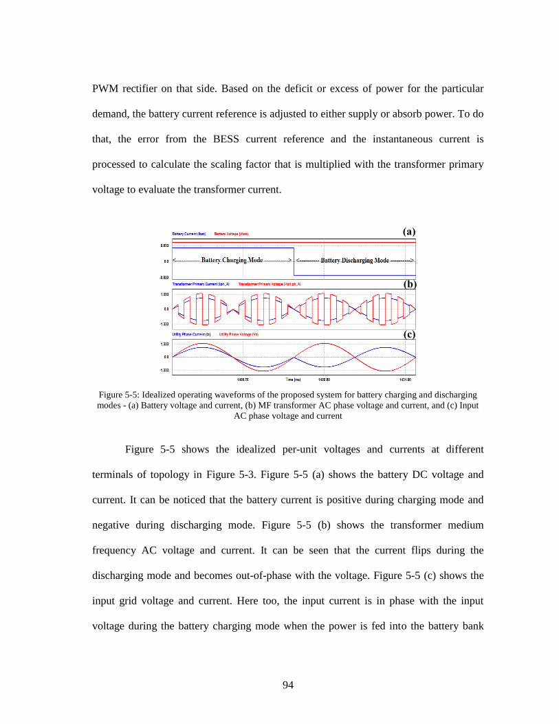
94
PWM rectifier on that side. Based on the deficit or excess of power for the particular
demand, the battery current reference is adjusted to either supply or absorb power. To do
that, the error from the BESS current reference and the instantaneous current is
processed to calculate the scaling factor that is multiplied with the transformer primary
voltage to evaluate the transformer current.
Figure 5-5: Idealized operating waveforms of the proposed system for battery charging and discharging
modes - (a) Battery voltage and current, (b) MF transformer AC phase voltage and current, and (c) Input
AC phase voltage and current
Figure 5-5 shows the idealized per-unit voltages and currents at different
terminals of topology in Figure 5-3. Figure 5-5 (a) shows the battery DC voltage and
current. It can be noticed that the battery current is positive during charging mode and
negative during discharging mode. Figure 5-5 (b) shows the transformer medium
frequency AC voltage and current. It can be seen that the current flips during the
discharging mode and becomes out-of-phase with the voltage. Figure 5-5 (c) shows the
input grid voltage and current. Here too, the input current is in phase with the input
voltage during the battery charging mode when the power is fed into the battery bank
(a)
(b)
(c)
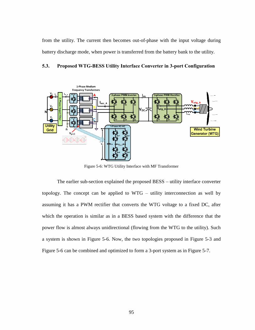
95
from the utility. The current then becomes out-of-phase with the input voltage during
battery discharge mode, when power is transferred from the battery bank to the utility.
5.3. Proposed WTG-BESS Utility Interface Converter in 3-port Configuration
Figure 5-6: WTG Utility Interface with MF Transformer
The earlier sub-section explained the proposed BESS – utility interface converter
topology. The concept can be applied to WTG – utility interconnection as well by
assuming it has a PWM rectifier that converts the WTG voltage to a fixed DC, after
which the operation is similar as in a BESS based system with the difference that the
power flow is almost always unidirectional (flowing from the WTG to the utility). Such
a system is shown in Figure 5-6. Now, the two topologies proposed in Figure 5-3 and
Figure 5-6 can be combined and optimized to form a 3-port system as in Figure 5-7.
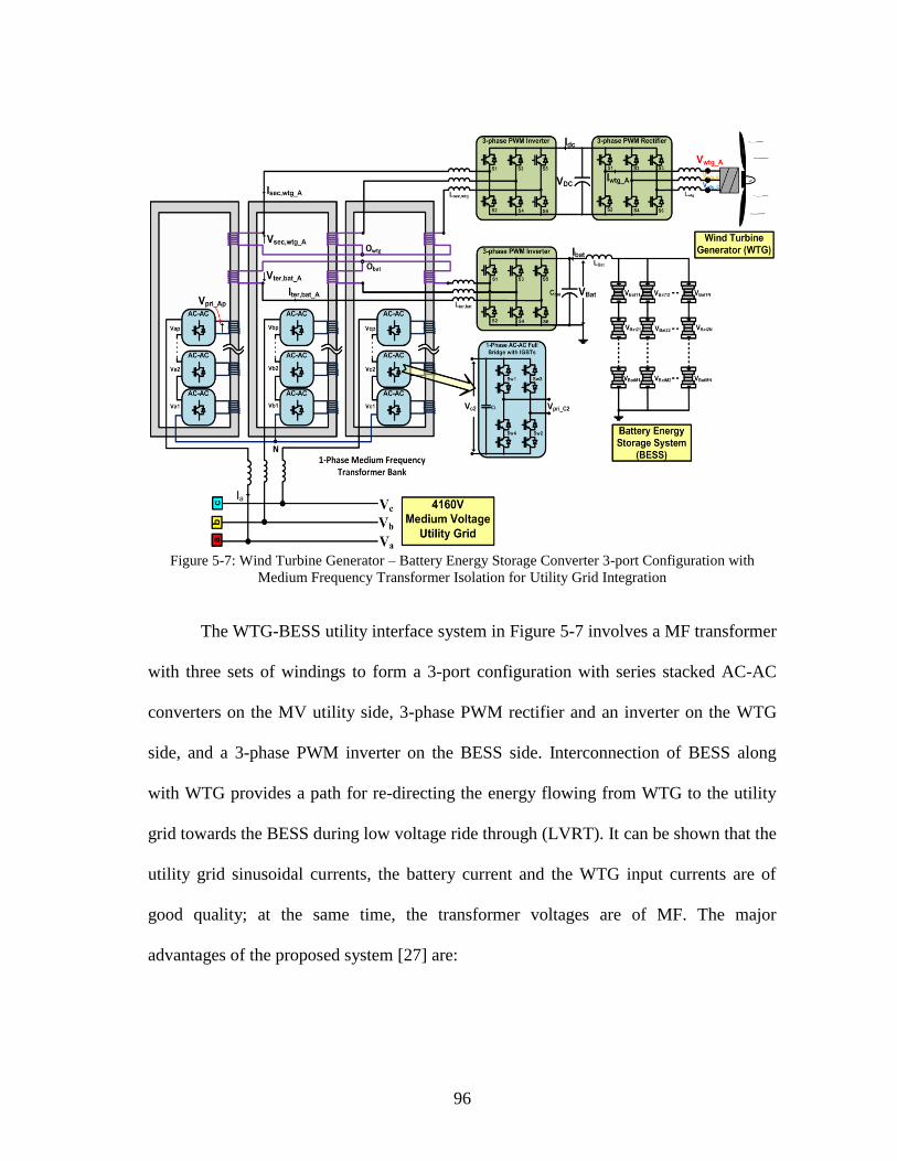
96
Figure 5-7: Wind Turbine Generator – Battery Energy Storage Converter 3-port Configuration with
Medium Frequency Transformer Isolation for Utility Grid Integration
The WTG-BESS utility interface system in Figure 5-7 involves a MF transformer
with three sets of windings to form a 3-port configuration with series stacked AC-AC
converters on the MV utility side, 3-phase PWM rectifier and an inverter on the WTG
side, and a 3-phase PWM inverter on the BESS side. Interconnection of BESS along
with WTG provides a path for re-directing the energy flowing from WTG to the utility
grid towards the BESS during low voltage ride through (LVRT). It can be shown that the
utility grid sinusoidal currents, the battery current and the WTG input currents are of
good quality; at the same time, the transformer voltages are of MF. The major
advantages of the proposed system [27] are:

97
• The MF link transformer provides galvanic isolation as well as proper voltage
matching between the utility, the WTG and the BESS. It also contributes to reduced
size/weight while maintaining good transfer efficiency.
• A single transformer can be used for interfacing both WTG and BESS systems to the
utility grid. The leakage inductances of the MF transformer are used as power transfer
reactors; there is no need for external inductors. One set of windings is reduced.
• The AC-AC converters and PWM rectifiers are modulated to make utility and WTG
power factor near unity.
• As the AC-AC converters are switched at MF, the switching losses are low.
• The controller can handle voltage sags and swells without any significant change in
topology or strategy.
• The proposed strategy is flexible, allows for high switching frequency operation on
the PWM rectifiers, ensuring that the transformer core is operated at constant MF
over entire range.
• LVRT can be implemented with minimal change in the topology.
The design of the entire topology in Figure 5-7 can be broadly divided into the
following 5 sub-sections as before: (1) Multi-level AC-AC converter, (2) WTG and
BESS, (3) 3-phase PWM rectifier and inverter, (4) Medium frequency transformer, and
(5) Control strategy.
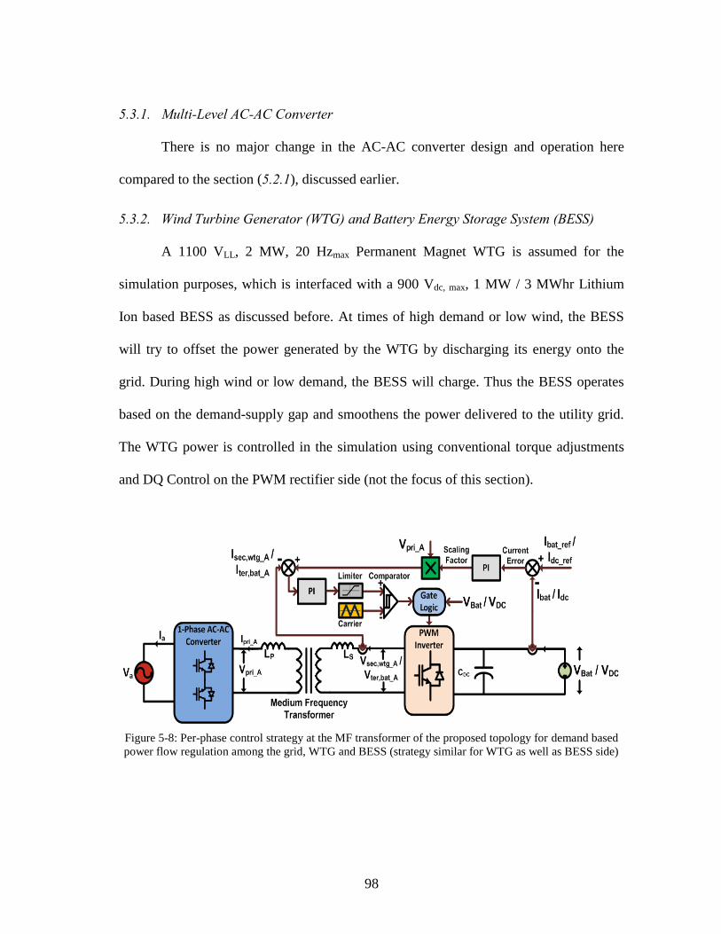
98
5.3.1. Multi-Level AC-AC Converter
There is no major change in the AC-AC converter design and operation here
compared to the section (5.2.1), discussed earlier.
5.3.2. Wind Turbine Generator (WTG) and Battery Energy Storage System (BESS)
A 1100 VLL, 2 MW, 20 Hzmax Permanent Magnet WTG is assumed for the
simulation purposes, which is interfaced with a 900 Vdc, max, 1 MW / 3 MWhr Lithium
Ion based BESS as discussed before. At times of high demand or low wind, the BESS
will try to offset the power generated by the WTG by discharging its energy onto the
grid. During high wind or low demand, the BESS will charge. Thus the BESS operates
based on the demand-supply gap and smoothens the power delivered to the utility grid.
The WTG power is controlled in the simulation using conventional torque adjustments
and DQ Control on the PWM rectifier side (not the focus of this section).
Figure 5-8: Per-phase control strategy at the MF transformer of the proposed topology for demand based
power flow regulation among the grid, WTG and BESS (strategy similar for WTG as well as BESS side)
99
5.3.3. 3-Phase PWM Rectifier and Inverter
Figure 5-8 shows a single-level per-phase diagram of the proposed topology
along with the control strategy. The voltage applied to the transformer primary, Vpri_A
induces voltages on the secondary winding Vsec,wtg_A as well as the tertiary winding
Vter,bat_A based on the turns-ratio. The PWM rectifier at the WTG side is governed by
conventional DQ control to transmit available wind power to the DC-Link. The DC-Link
voltage on the WTG side, VDC is regulated at 1500 V, suitable for the PWM inverter
operation. Operation and control of PWM inverters on the secondary and tertiary
windings is similar. Thus, the switching function of the PWM inverters is the same as
discussed earlier, must be a product of a line frequency sine wave and a MF square
wave. The power transfer equations are also similar and given by (5.1) and (5.2). The
proposed topology in Figure 5-7 has only one set of transformer tertiary windings with a
3-phase PWM inverter for BESS. But this modular system can be expanded in terms of
power rating by adding more windings along with PWM inverters and battery banks.
5.3.4. Medium Frequency (MF) Transformer
Medium frequency (MF) transformer design is detailed under section 6.
5.3.5. Control Strategy
The detailed control strategy adopted for the proposed system can be seen in
Figure 5-8 (only one transformer phase is shown for simplicity, but it also applies for
other transformer phases of the topology in Figure 5-7) for controlling the power flow
from the WTG to the utility grid as well as charging/discharging of BESS. The control
mechanism is exactly the same as before, consists of two current loops – (a) the external
100
loop regulating the DC current, Ibat or Idc and (b) the internal loop regulating the
transformer secondary/ tertiary currents, Isec,wtg_A and Iter,bat_A.
It may be noted that the WTG is controlled in such a way that it is always desired
to derive the maximum power out of it. Based on the deficit or excess of power for the
particular demand, the battery current reference is adjusted to either supply or absorb
power. To do that, the error from the BESS current reference and the instantaneous
current is processed to calculate the scaling factor that is multiplied with the transformer
primary voltage to evaluate the transformer current.
Now at the WTG side PWM rectifier, DQ control regulates the DC-Link voltage.
The PWM inverter on the WTG side works similar to that on the BESS side, only that
the reference for the DC-link current comes from the WTG available power at any
instant. The inner PI controller can be replaced with hysteresis controller, which will
also yield similar performance. It should be noted that as there is a single common outer
loop and scaling factor, any imbalance in the transformer phase currents will be avoided
as the control will make sure that the power is transferred equally across all the phases. It
will also help in appropriate division of voltage between the windings of multiple levels.
Since the power flow mechanism is a current control scheme, both sides of the B-H
curve are used in the transformer and thus the core saturation can be reduced. The utility
currents will have small amount of twice the MF components due to transformer current
transients; these harmonics can be filtered using an LC filter.
101
5.4. Low Voltage Ride Through (LVRT) Capability
WTGs are generally required to be capable of LVRT when the voltage in the grid
is temporarily reduced due to a fault or load change in the grid. The voltage may be
reduced in one, two or all the three phases of the AC grid. The severity of the voltage
sag depends upon the voltage level it reduces to and the duration [81-83].
In USA, the Federal Energy Regulatory Commission (FERC) specifies an LVRT
requirement in Appendix G of its Order No. 661, Large Generator Interconnection
Agreement (LGIA) which was issued on June 2, 2005. An applicable WTG would be
required to remain operational during a grid fault as shown in Figure 5-9. NERC
proposed a more stringent requirement for WTGs to remain online even with grid
voltage falling to zero volts for a few cycles [82, 83]. During unbalanced voltage sags,
the grid codes require wind turbine utilities to reduce the active power and supply
reactive power to support the grid till the grid comes back to normal.
In a conventional WTG system (Figure 4-1) when disturbance occurs in the
utility grid, the voltage at the AC output terminals of the WTG drops. The output power
of the inverter can be quickly reduced. However, the power generated by WTG cannot
be reduced at the same rate. This creates an energy mismatch between the power
generated by the WTG and the power delivered to the utility grid. This energy difference
will cause a voltage surge at the DC-link capacitor. A very large voltage may damage
the power devices as well as the capacitor [83]. These issues need to be overcome while
incorporating LVRT capability. One way to reduce the voltage surge is by dumping the

102
excess energy into a DC-link chopper as shown in Figure 5-10. If the energy mismatch is
large, then the chopper rating has to be sufficiently high.
Figure 5-9: Energy Profile during conventional LVRT
Figure 5-10: Conventional WTG Power Converter with chopper circuit for LVRT Capability [83]
Figure 5-11: Energy profile during LVRT for the proposed topology with DC-link chopper (bleeder)
103
Figure 5-9 shows the energy profile of WTG during a fault condition, along with
DC-link chopper based LVRT capability. It can be seen that the energy to be dissipated
in the chopper is large (indicated by the shaded area) as the WTG takes some finite time
to activate pitch control and reach a low power stage. During this time, there is a larger
tendency of the DC-Link capacitor voltage to increase unless the chopper can absorb the
excess energy during temporary fault. The WTG system has to be tripped if the fault
persists for more than the stipulated number of cycles.
In the proposed system, the BESS can be controlled to reduce the amount of
active power to be supplied to the grid. In case the BESS does not have enough rating to
absorb any more current, a DC Chopper can be used to dump excess energy. The BESS
can also supply reactive current during the sag. The controller determines the amount of
reactive power to be supplied and commands tertiary battery current to be out of phase
of tertiary voltages by the required angle. Once the grid is back to normal, the phase is
reduced to zero and the normal supply of active power to the grid is resumed.
Figure 5-11 shows the methodology that can be employed using the proposed
system for LVRT capability. When a fault occurs, it is quickly sensed and the BESS
system will start absorbing the WTG energy. Just in case the WTG is operating at full
power and the BESS is not rated for power equal to the WTG, a chopper circuit is still
required, but the rating can be much smaller as the excess energy that needs to be
dissipated is small (shown by the shaded area in Figure 5-11). The AC-AC converter at
the utility side is switched normally during fault. The chopper will stop once it has
consumed the excess energy. The BESS delivers the required reactive current to support
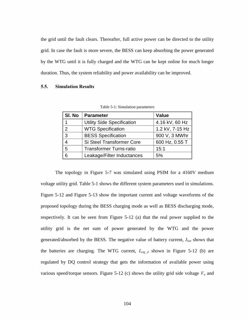
104
the grid until the fault clears. Thereafter, full active power can be directed to the utility
grid. In case the fault is more severe, the BESS can keep absorbing the power generated
by the WTG until it is fully charged and the WTG can be kept online for much longer
duration. Thus, the system reliability and power availability can be improved.
5.5. Simulation Results
Table 5-1: Simulation parameters
Sl. No Parameter Value
1 Utility Side Specification 4.16 kV, 60 Hz
2 WTG Specification 1.2 kV, 7-15 Hz
3 BESS Specification 900 V, 3 MWhr
4 Si Steel Transformer Core 600 Hz, 0.55 T
5 Transformer Turns-ratio 15:1
6 Leakage/Filter Inductances 5%
The topology in Figure 5-7 was simulated using PSIM for a 4160V medium
voltage utility grid. Table 5-1 shows the different system parameters used in simulations.
Figure 5-12 and Figure 5-13 show the important current and voltage waveforms of the
proposed topology during the BESS charging mode as well as BESS discharging mode,
respectively. It can be seen from Figure 5-12 (a) that the real power supplied to the
utility grid is the net sum of power generated by the WTG and the power
generated/absorbed by the BESS. The negative value of battery current, Ibat shows that
the batteries are charging. The WTG current, Iwtg_A shown in Figure 5-12 (b) are
regulated by DQ control strategy that gets the information of available power using
various speed/torque sensors. Figure 5-12 (c) shows the utility grid side voltage Va and
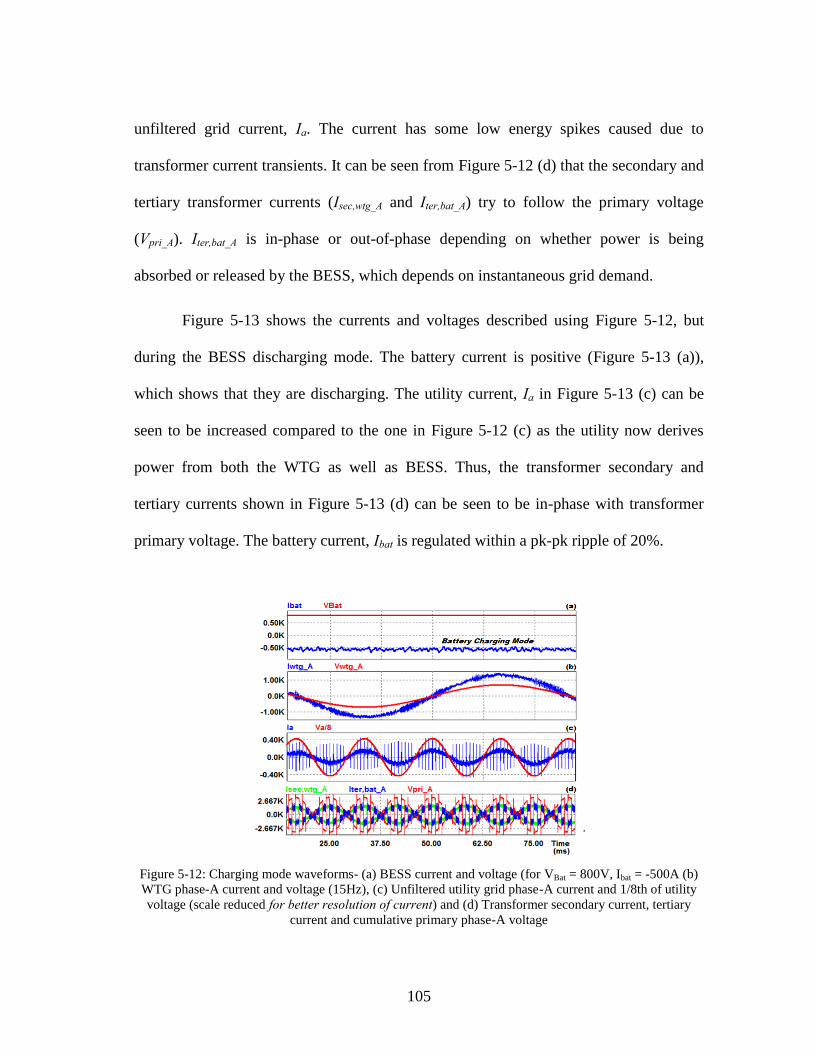
105
unfiltered grid current, Ia. The current has some low energy spikes caused due to
transformer current transients. It can be seen from Figure 5-12 (d) that the secondary and
tertiary transformer currents (Isec,wtg_A and Iter,bat_A) try to follow the primary voltage
(Vpri_A). Iter,bat_A is in-phase or out-of-phase depending on whether power is being
absorbed or released by the BESS, which depends on instantaneous grid demand.
Figure 5-13 shows the currents and voltages described using Figure 5-12, but
during the BESS discharging mode. The battery current is positive (Figure 5-13 (a)),
which shows that they are discharging. The utility current, Ia in Figure 5-13 (c) can be
seen to be increased compared to the one in Figure 5-12 (c) as the utility now derives
power from both the WTG as well as BESS. Thus, the transformer secondary and
tertiary currents shown in Figure 5-13 (d) can be seen to be in-phase with transformer
primary voltage. The battery current, Ibat is regulated within a pk-pk ripple of 20%.
Figure 5-12: Charging mode waveforms- (a) BESS current and voltage (for VBat = 800V, Ibat = -500A (b)
WTG phase-A current and voltage (15Hz), (c) Unfiltered utility grid phase-A current and 1/8th of utility
voltage (scale reduced for better resolution of current) and (d) Transformer secondary current, tertiary
current and cumulative primary phase-A voltage
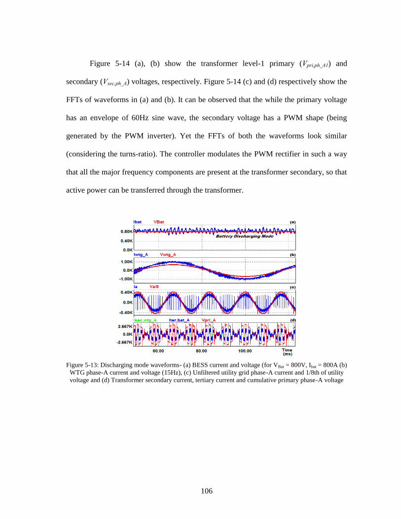
106
Figure 5-14 (a), (b) show the transformer level-1 primary (Vpri,ph_A1) and
secondary (Vsec,ph_A) voltages, respectively. Figure 5-14 (c) and (d) respectively show the
FFTs of waveforms in (a) and (b). It can be observed that the while the primary voltage
has an envelope of 60Hz sine wave, the secondary voltage has a PWM shape (being
generated by the PWM inverter). Yet the FFTs of both the waveforms look similar
(considering the turns-ratio). The controller modulates the PWM rectifier in such a way
that all the major frequency components are present at the transformer secondary, so that
active power can be transferred through the transformer.
Figure 5-13: Discharging mode waveforms- (a) BESS current and voltage (for VBat = 800V, Ibat = 800A (b)
WTG phase-A current and voltage (15Hz), (c) Unfiltered utility grid phase-A current and 1/8th of utility
voltage and (d) Transformer secondary current, tertiary current and cumulative primary phase-A voltage

107
Figure 5-14: (a) Transformer phase-A primary voltage, (b) Transformer phase-A secondary voltage, (c)
and (d) are respectively FFTs of (a) and (b)
Figure 5-15 shows variation in utility grid current with respect to slow step
changes in BESS current as well as WTG generated power. It can be seen that for a short
time, the power generated by WTG is entirely used to charge the BESS. The net power
between the utility, WTG and BESS are seen to be properly balanced. Figure 5-16 (a)
shows the LVRT functionality of the proposed system when WTG is delivering full
power (2MW) and a fault occurs at phase-A. It can be seen that the DC-Link voltage
rises only around 20%. The DC-link chopper circuit operates when the voltage crosses
1800V and quickly brings the capacitor voltage back to normal, because the BESS is
absorbing the power from the WTG and the utility is drawing only a small amount of
active power during this time as required. Thus, the WTG does not have to be tripped
even if the fault prolongs for some more time. Figure 5-16 (b) shows that the converter
can support the grid with reactive power during LVRT.
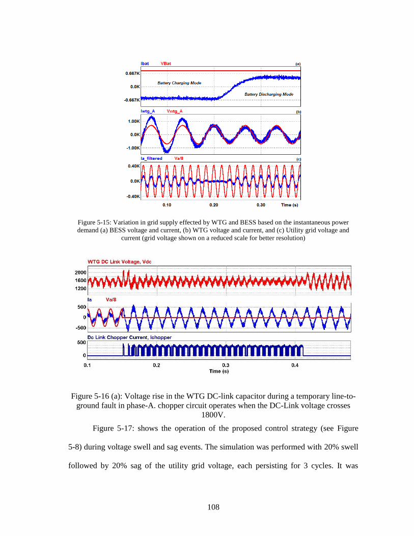
108
Figure 5-15: Variation in grid supply effected by WTG and BESS based on the instantaneous power
demand (a) BESS voltage and current, (b) WTG voltage and current, and (c) Utility grid voltage and
current (grid voltage shown on a reduced scale for better resolution)
Figure 5-16 (a): Voltage rise in the WTG DC-link capacitor during a temporary line-to-
ground fault in phase-A. chopper circuit operates when the DC-Link voltage crosses
1800V.
Figure 5-17: shows the operation of the proposed control strategy (see Figure
5-8) during voltage swell and sag events. The simulation was performed with 20% swell
followed by 20% sag of the utility grid voltage, each persisting for 3 cycles. It was
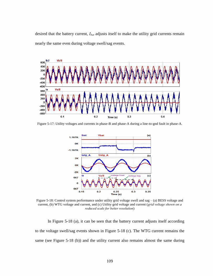
109
desired that the battery current, Ibat adjusts itself to make the utility grid currents remain
nearly the same even during voltage swell/sag events.
Figure 5-17: Utility voltages and currents in phase-B and phase-A during a line-to-gnd fault in phase-A.
Figure 5-18: Control system performance under utility grid voltage swell and sag – (a) BESS voltage and
current, (b) WTG voltage and current, and (c) Utility grid voltage and current (grid voltage shown on a reduced scale for better resolution)
In Figure 5-18 (a), it can be seen that the battery current adjusts itself according
to the voltage swell/sag events shown in Figure 5-18 (c). The WTG current remains the
same (see Figure 5-18 (b)) and the utility current also remains almost the same during
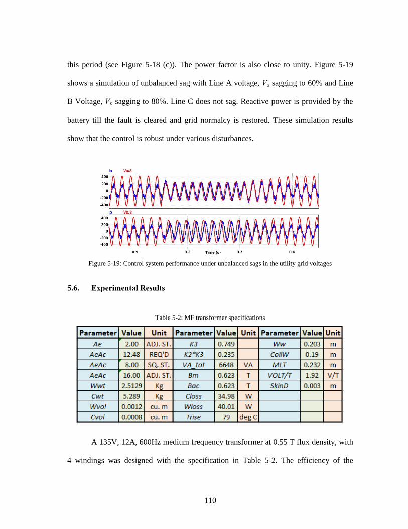
110
this period (see Figure 5-18 (c)). The power factor is also close to unity. Figure 5-19
shows a simulation of unbalanced sag with Line A voltage, Va sagging to 60% and Line
B Voltage, Vb sagging to 80%. Line C does not sag. Reactive power is provided by the
battery till the fault is cleared and grid normalcy is restored. These simulation results
show that the control is robust under various disturbances.
Figure 5-19: Control system performance under unbalanced sags in the utility grid voltages
5.6. Experimental Results
Table 5-2: MF transformer specifications
A 135V, 12A, 600Hz medium frequency transformer at 0.55 T flux density, with
4 windings was designed with the specification in Table 5-2. The efficiency of the
111
transformer was found by experiment to be around 97.5%. The next step was to analyze
how the transformer core loss varies with the type of waveform it is operated with. For
this, a scaled down prototype similar to the set-up in Figure 5-8 was built. Figure 5-20
shows AC-AC converter experimental waveforms from the prototype when supplied
with 120 V utility voltage and with a resistive load of 1.2 kW on the secondary side,
when the primary is switched with square wave modulation. Figure 5-20 also shows the
thermal image of the MF transformer under test. With the core temperature rise test, it is
not possible to assess the exact loss, but it provided an insight about the relative core loss
variation for different waveforms. Same rms voltages and loads were applied to the
transformer using the converter for the following operating conditions – i) 600 Hz sine,
ii) 60 Hz sine multiplied by 600 Hz square modulation and iii) 60 Hz sine multiplied by
570 Hz square modulation. The transformer was kept running for 2 hours for each of the
above conditions and the core temperatures were monitored using a thermal camera
(assuming similar conduction losses).
Figure 5-21 shows the closed loop control waveforms of transformer primary and
secondary voltages and current with a DC source on the secondary side as in Figure 5-8.
The secondary side PWM inverter was switched at 12 kHz. The current in the
transformer was regulated at the desired set point of 5A. It can be seen from Figure 5-21
that there are some high frequency components in the transformer primary current,
which can be attributed to the PWM carrier frequency on the inverter that induces the
current control. These components are eliminated by the filter on the utility side to
maintain near-unity power factor. Since they are of low energy, LC filter will be small.
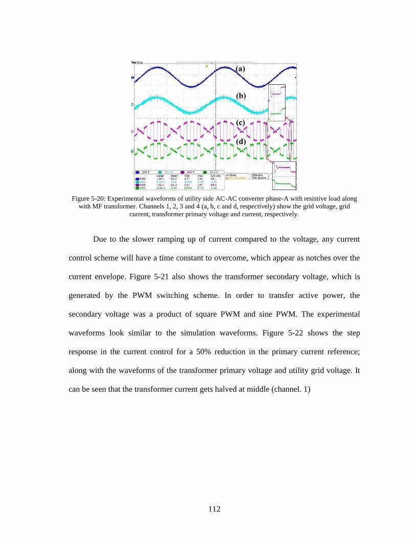
112
Figure 5-20: Experimental waveforms of utility side AC-AC converter phase-A with resistive load along
with MF transformer. Channels 1, 2, 3 and 4 (a, b, c and d, respectively) show the grid voltage, grid
current, transformer primary voltage and current, respectively.
Due to the slower ramping up of current compared to the voltage, any current
control scheme will have a time constant to overcome, which appear as notches over the
current envelope. Figure 5-21 also shows the transformer secondary voltage, which is
generated by the PWM switching scheme. In order to transfer active power, the
secondary voltage was a product of square PWM and sine PWM. The experimental
waveforms look similar to the simulation waveforms. Figure 5-22 shows the step
response in the current control for a 50% reduction in the primary current reference;
along with the waveforms of the transformer primary voltage and utility grid voltage. It
can be seen that the transformer current gets halved at middle (channel. 1)
(a)
(b)
(c)
(d)
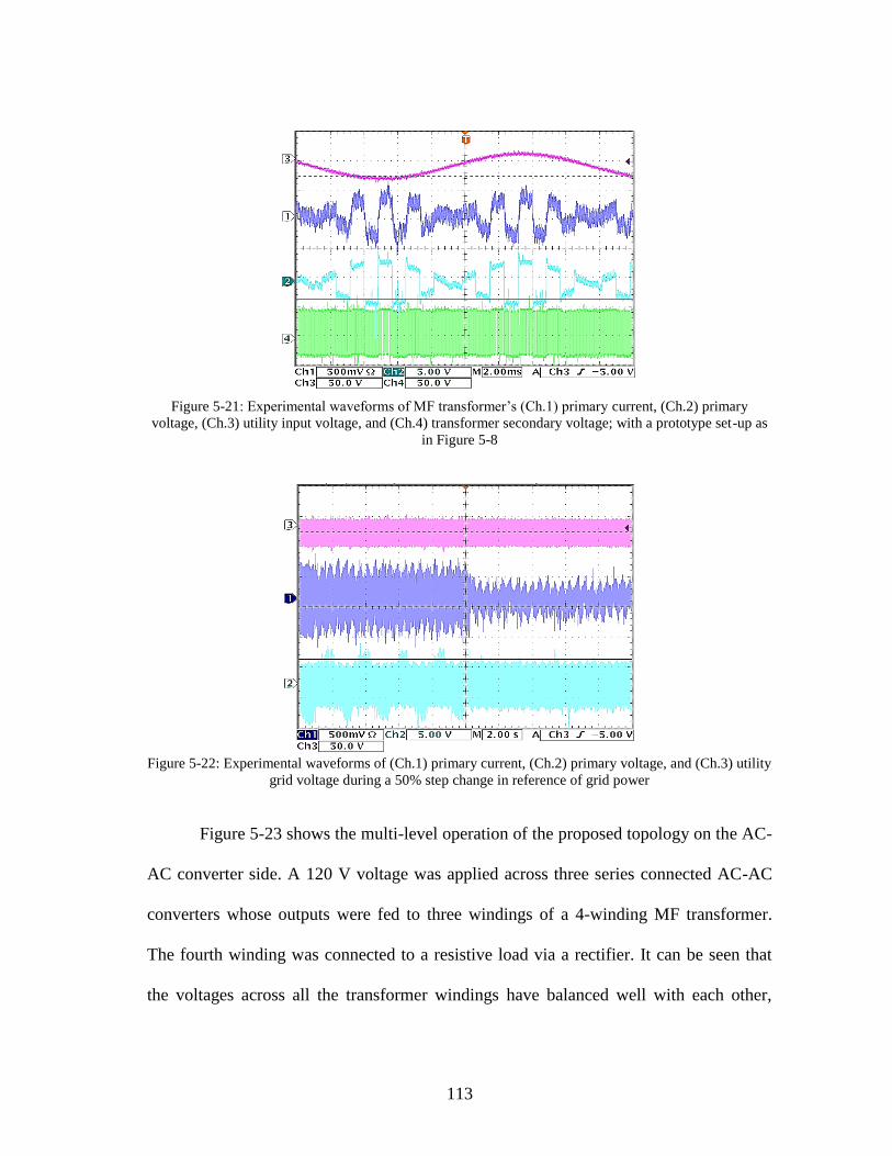
113
Figure 5-21: Experimental waveforms of MF transformer’s (Ch.1) primary current, (Ch.2) primary
voltage, (Ch.3) utility input voltage, and (Ch.4) transformer secondary voltage; with a prototype set-up as
in Figure 5-8
Figure 5-22: Experimental waveforms of (Ch.1) primary current, (Ch.2) primary voltage, and (Ch.3) utility
grid voltage during a 50% step change in reference of grid power
Figure 5-23 shows the multi-level operation of the proposed topology on the AC-
AC converter side. A 120 V voltage was applied across three series connected AC-AC
converters whose outputs were fed to three windings of a 4-winding MF transformer.
The fourth winding was connected to a resistive load via a rectifier. It can be seen that
the voltages across all the transformer windings have balanced well with each other,

114
which proves that series-stacking multiple levels of AC-AC converters is possible in the
proposed topologies. Figure 5-24 shows a section of the experimental set-up used for
this topology, including the 600 Hz MF transformer and AC-AC converter.
Figure 5-23: Multilevel Operation of AC-AC converter with a 4-winding MF transformer of 600 Hz
connected with multilevel structure of AC-AC converters.
5.7. Conclusion
Three new topologies were proposed in this section for MV utility interface of
wind turbine generators as well as battery energy storage systems. The basic concepts of
the topologies and the main design equations for the voltages involving AC-AC
converters, PWM rectifier and inverters were elucidated. Overall system simulation
results of a 2MW WTG - BESS system were shown and experimental waveforms from

115
scaled down prototype were presented. This paper provided detailed analysis of the
converter, along with extensive simulation results. An improved low voltage ride
through (LVRT) technique was also proposed for the WTG system that needed only
minor modifications in the topology. Overall, the proposed topologies resulted in smaller
size and weight along with good quality power delivery that can be achieved at a
competitive cost.
Figure 5-24: Experimental set-up, showing the 600 Hz MF transformer and AC-AC converter
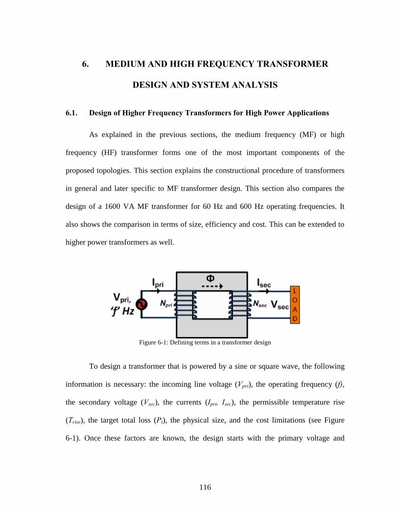
116
6. MEDIUM AND HIGH FREQUENCY TRANSFORMER
DESIGN AND SYSTEM ANALYSIS
6.1. Design of Higher Frequency Transformers for High Power Applications
As explained in the previous sections, the medium frequency (MF) or high
frequency (HF) transformer forms one of the most important components of the
proposed topologies. This section explains the constructional procedure of transformers
in general and later specific to MF transformer design. This section also compares the
design of a 1600 VA MF transformer for 60 Hz and 600 Hz operating frequencies. It
also shows the comparison in terms of size, efficiency and cost. This can be extended to
higher power transformers as well.
Figure 6-1: Defining terms in a transformer design
To design a transformer that is powered by a sine or square wave, the following
information is necessary: the incoming line voltage (Vpri), the operating frequency (f),
the secondary voltage (Vsec), the currents (Ipri, Isec), the permissible temperature rise
(Trise), the target total loss (Pt), the physical size, and the cost limitations (see Figure
6-1). Once these factors are known, the design starts with the primary voltage and
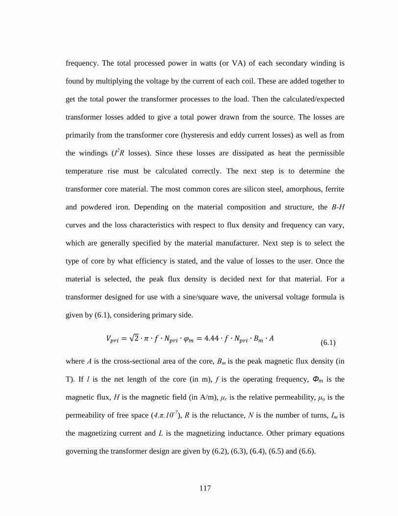
117
(6.1)
frequency. The total processed power in watts (or VA) of each secondary winding is
found by multiplying the voltage by the current of each coil. These are added together to
get the total power the transformer processes to the load. Then the calculated/expected
transformer losses added to give a total power drawn from the source. The losses are
primarily from the transformer core (hysteresis and eddy current losses) as well as from
the windings (I2R losses). Since these losses are dissipated as heat the permissible
temperature rise must be calculated correctly. The next step is to determine the
transformer core material. The most common cores are silicon steel, amorphous, ferrite
and powdered iron. Depending on the material composition and structure, the B-H
curves and the loss characteristics with respect to flux density and frequency can vary,
which are generally specified by the material manufacturer. Next step is to select the
type of core by what efficiency is stated, and the value of losses to the user. Once the
material is selected, the peak flux density is decided next for that material. For a
transformer designed for use with a sine/square wave, the universal voltage formula is
given by (6.1), considering primary side.
𝑉𝑝𝑟𝑖 = √2 ∙ 𝜋 ∙ 𝑓 ∙ 𝑁𝑝𝑟𝑖 ∙ 𝜑𝑚 = 4.44 ∙ 𝑓 ∙ 𝑁𝑝𝑟𝑖 ∙ 𝐵𝑚 ∙ 𝐴
where A is the cross-sectional area of the core, Bm is the peak magnetic flux density (in
T). If l is the net length of the core (in m), f is the operating frequency, Фm is the
magnetic flux, H is the magnetic field (in A/m), μr is the relative permeability, μo is the
permeability of free space (4.π.10-7), R is the reluctance, N is the number of turns, Im is
the magnetizing current and L is the magnetizing inductance. Other primary equations
governing the transformer design are given by (6.2), (6.3), (6.4), (6.5) and (6.6).

118
𝑁𝑝𝑟𝑖
𝑁𝑠𝑒𝑐=
𝑉𝑝𝑟𝑖
𝑉𝑠𝑒𝑐=
𝐼𝑠𝑒𝑐
𝐼𝑝𝑟𝑖
𝜑𝑛𝑒𝑡 =𝑀.𝑀. 𝐹𝑛𝑒𝑡
𝑅=
(𝑁𝑝𝑟𝑖 ∙ 𝐼𝑝𝑟𝑖 − 𝑁𝑠𝑒𝑐 ∙ 𝐼𝑠𝑒𝑐)
𝑅
𝐻𝑛𝑒𝑡 =(𝑁𝑝𝑟𝑖∙𝐼𝑝𝑟𝑖−𝑁𝑠𝑒𝑐∙𝐼𝑠𝑒𝑐)
𝑙 =
𝑁∙𝐼𝑚
𝑙
𝑅 =𝑙
𝜇𝑟 ∙ 𝜇𝑜 ∙ 𝐴
𝐿 =𝑁𝑝𝑟𝑖 ∙ 𝐵 ∙ 𝐴
𝐼𝑝𝑟𝑖=
𝜇𝑟 ∙ 𝜇𝑜 ∙ 𝐴 ∙ 𝑁𝑝𝑟𝑖2
𝑙
From these equations, the transformer can be designed by following the below
procedure [84-86]:
1. Select an operating frequency for the transformer (say 60 Hz, 600 Hz, etc.)
depending on the application and specifications
2. Based on the power curves available for different cores, select the particular type
of core material to use for the particular frequency. In order to use for
applications such as ASDs, WTGs, etc., for frequencies less than 1 kHz silicon
steel or amorphous core can be used, but would require other core materials such
as ferrite in order to use at much higher frequencies.
3. Once the core is decided, using the voltage, current and peak flux density
specifications, eqn. (6.1) is used to determine the minimum ‘A*N’ value.
(6.2)
(6.4)
(6.5)
(6.6)
(6.3)

119
4. After that, a minimum value of magnetizing inductance, L is calculated for the
selected frequency so that the magnetizing current, Im (this is approximately “Ipri
– Isec” for a 1:1 transformer) is small, say less than 5 % of the transformer current
rating.
5. With the expected L value, choose an ‘Npri’ value. Then this value is used in (6.4)
to arrive at a minimum length of the core.
6. Using the inequalities arrived at using equations (6.1), (6.4) and (6.6), the
dimensions of the transformer and number of turns can be decided. Another
constraint in this can be given by the net window area of the transformer core,
which is determined by the total area of the conductors carrying the current. This
factor also plays an important role in the decision of the total core length, l.
7. With the arrived dimensions, the total power loss, hence the efficiency of the
transformer can be calculated. If it is either lower or higher than expected, the
design steps have to be repeated with different values for number of turns,
magnetizing current, etc. until the final specification is met.
6.2. Magnetization Characteristics of Different Transformer Core Materials
Substituting the specification values into the above equations, it is possible to
decide the primary number of turns, flux density, area, etc. Depending upon the core
material, the performance and design vary significantly. For the silicon steel B-H curve
shown in Figure 6-2, the saturation flux density is above 1.5 T and the saturation does
not happen until high magnetic fields of about 800 A/m. Due to this reason, the length of
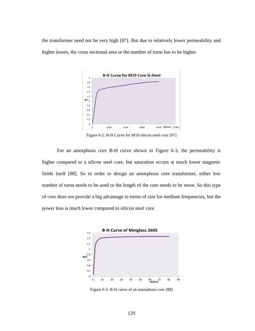
120
the transformer need not be very high [87]. But due to relatively lower permeability and
higher losses, the cross sectional area or the number of turns has to be higher.
Figure 6-2: B-H Curve for M19 silicon steel core [87]
For an amorphous core B-H curve shown in Figure 6-3, the permeability is
higher compared to a silicon steel core, but saturation occurs at much lower magnetic
fields itself [88]. So in order to design an amorphous core transformer, either low
number of turns needs to be used or the length of the core needs to be more. So this type
of core does not provide a big advantage in terms of size for medium frequencies, but the
power loss is much lower compared to silicon steel core.
Figure 6-3: B-H curve of an amorphous core [88]
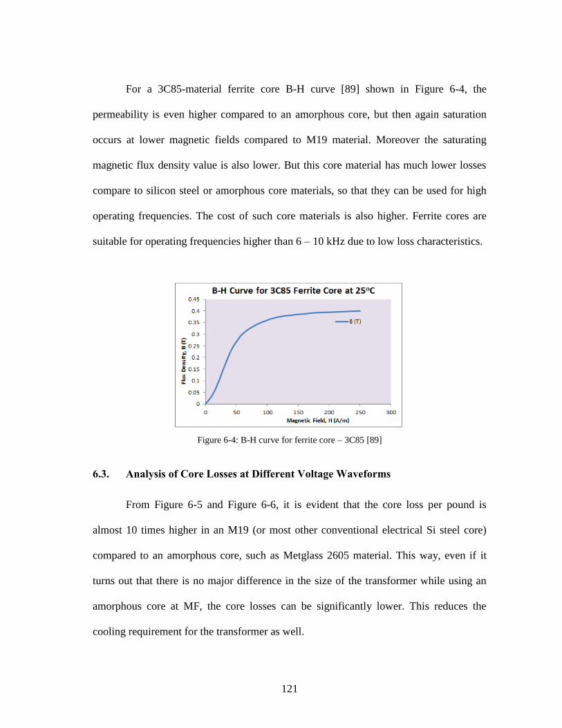
121
For a 3C85-material ferrite core B-H curve [89] shown in Figure 6-4, the
permeability is even higher compared to an amorphous core, but then again saturation
occurs at lower magnetic fields compared to M19 material. Moreover the saturating
magnetic flux density value is also lower. But this core material has much lower losses
compare to silicon steel or amorphous core materials, so that they can be used for high
operating frequencies. The cost of such core materials is also higher. Ferrite cores are
suitable for operating frequencies higher than 6 – 10 kHz due to low loss characteristics.
Figure 6-4: B-H curve for ferrite core – 3C85 [89]
6.3. Analysis of Core Losses at Different Voltage Waveforms
From Figure 6-5 and Figure 6-6, it is evident that the core loss per pound is
almost 10 times higher in an M19 (or most other conventional electrical Si steel core)
compared to an amorphous core, such as Metglass 2605 material. This way, even if it
turns out that there is no major difference in the size of the transformer while using an
amorphous core at MF, the core losses can be significantly lower. This reduces the
cooling requirement for the transformer as well.
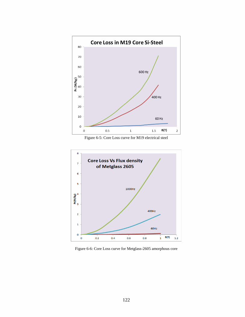
122
Figure 6-5: Core Loss curve for M19 electrical steel
Figure 6-6: Core Loss curve for Metglass-2605 amorphous core
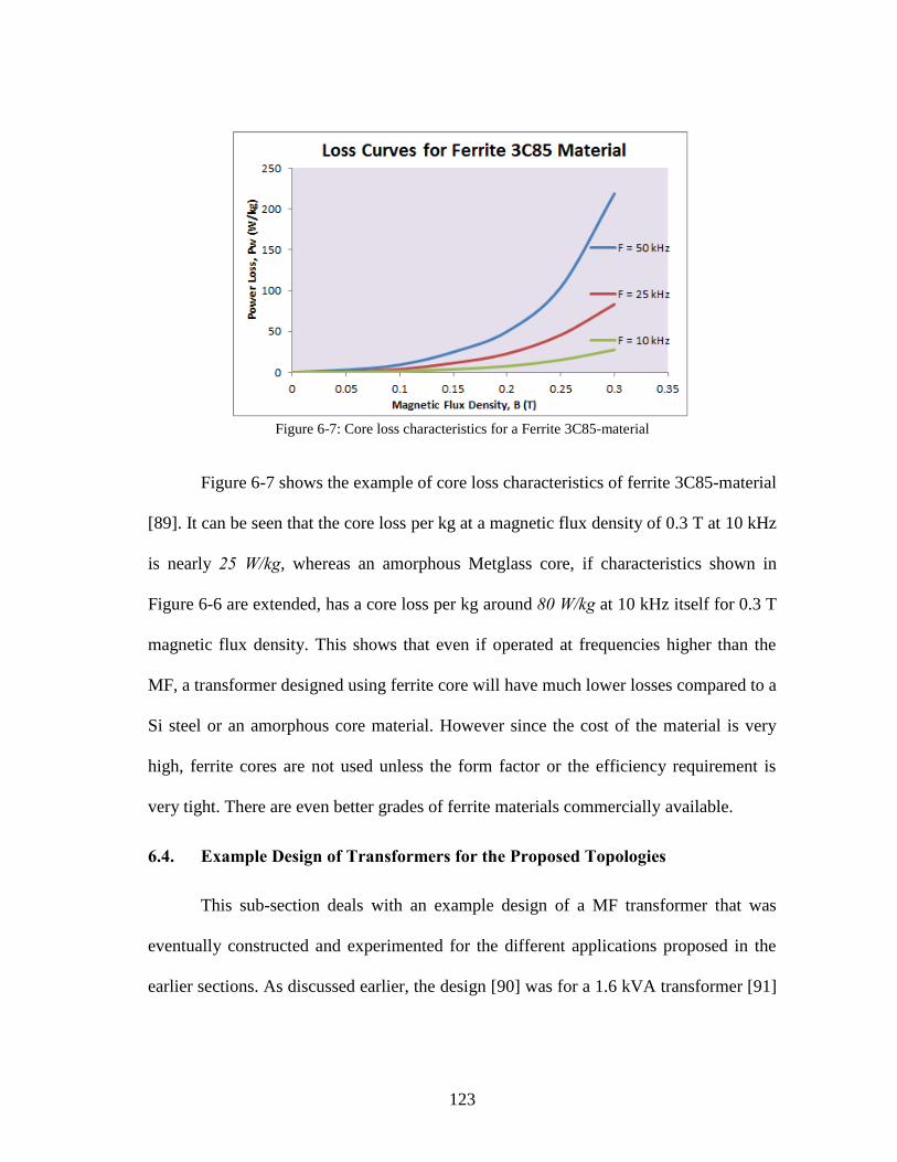
123
Figure 6-7: Core loss characteristics for a Ferrite 3C85-material
Figure 6-7 shows the example of core loss characteristics of ferrite 3C85-material
[89]. It can be seen that the core loss per kg at a magnetic flux density of 0.3 T at 10 kHz
is nearly 25 W/kg, whereas an amorphous Metglass core, if characteristics shown in
Figure 6-6 are extended, has a core loss per kg around 80 W/kg at 10 kHz itself for 0.3 T
magnetic flux density. This shows that even if operated at frequencies higher than the
MF, a transformer designed using ferrite core will have much lower losses compared to a
Si steel or an amorphous core material. However since the cost of the material is very
high, ferrite cores are not used unless the form factor or the efficiency requirement is
very tight. There are even better grades of ferrite materials commercially available.
6.4. Example Design of Transformers for the Proposed Topologies
This sub-section deals with an example design of a MF transformer that was
eventually constructed and experimented for the different applications proposed in the
earlier sections. As discussed earlier, the design [90] was for a 1.6 kVA transformer [91]

124
with a peak voltage rating of around 130 V. First, a 60 Hz transformer reference was
designed, focusing on the least size aspect without saturating the core. Considering the
M-19 Si steel core (with magnetic and loss characteristics as in Figure 6-2 and Figure
6-5, respectively), the maximum flux density was limited to 1.25 T (which implies
magnetic field, H < 500 A/m) to avoid saturation. From (6.1), the relation between A and
N can be determined as in (6.7).
𝐴 ∙ 𝑁 ≥ 0.43
To reduce the magnetizing current to less than 0.5 A (< 5 % of rated current),
using (6.4), the relation between N and l can be given by (6.8).
𝑁
𝑙≤ 1000
Assuming AWG-14 wires are used with a current rating of at least 15 A with an
area of cross section of 2*10(-6)
m2, and a winding fill factor of 0.4 [90], another relation
between N and l can be arrived at using the equation (6.9) (assuming the window area,
Aw for this design as a function of core length l is given by Aw = l2/18).
𝑙2
18≥
2∗10(−6)∗2∗𝑁
0.4→
𝑙2
𝑁≥ 0.00018
One more inequality can be derived using (6.6). Considering that the maximum
magnetizing current can be 0.5 A at 130 V maximum excitation and 60 Hz frequency,
and assuming the maximum permeability of M-19 core in the region of interest is
0.0025, the inductance must be greater than 0.7 H. Then eqn. (6.6) leads to (6.10).
(6.7)
(6.8)
(6.9)

125
𝐴∙𝑁2
𝑙≥ 280
Solving the inequalities in (6.7), (6.8), (6.9) and (6.10), the below values given
by (6.11) were arrived at for the 60 Hz transformer:
𝑁60 = 250; 𝑙60 = 0.62 𝑚; 𝐴60 ≥ 0.003 𝑚2
Following similar arguments, a 600 Hz medium frequency (MF) transformer was
also designed for the same specifications with the same electrical steel core and targeting
same efficiency. The minor variations in the design are that the maximum flux density
for the 600 Hz transformer was limited to nearly 0.55 T even at 130 V. So the maximum
permeability for the range of interest is around 0.0035 T.m/A. Also, the fill factor in this
case was reduced to 0.3, due to the higher operating frequency. Finally, the below design
parameters were arrived at for the 600 Hz transformer, given by (6.12):
𝑁600 = 140; 𝑙600 = 0.54 𝑚; 𝐴600 ≥ 0.0012 𝑚2
From (6.11) and (6.12), it can be clearly seen that the overall core volume of the
MF transformer was reduced to almost 35 % of the 60 Hz core. These design
calculations can be extended to higher power transformers too, with slight changes in
peak flux densities and fill factors. Due to almost 2.5 times larger cross-sectional area
and more than 1.6 times increase in the number of turns of the 60 Hz transformer over
the 600 Hz transformer design, the total copper length required by the 60 Hz transformer
is almost 4 times that of the 600 Hz design, which increases the conduction losses. Using
the core loss curves of M19 core from Figure 6-5, it can be seen that the core loss per kg
of the 60 Hz design at 1.3 T is almost 4.5 times that of the 600 Hz design at 0.55 T. But
(6.10)
(6.11)
(6.12)

126
considering that the total weight of the 60 Hz core is at least 3 times that of the 600 Hz
transformer, the net core loss is only increased by 50 %. Considering the conduction
losses, the total transformer losses in the 60 Hz design as well as 600 Hz design are
almost similar.
A third transformer was designed using the amorphous Metglass core material
whose characteristics are shown in Figure 6-3 and Figure 6-6. Based on the B-H curve,
the maximum flux density was limited to 1.1 T to avoid core saturation (at a magnetic
field of close to 2.4 A/m and maximum permeability of 0.45 T.m/A). As discussed
before, due to the low magnetic field for saturation (3 A/m) and at 600 Hz, the design
parameters resulted in almost the same dimensions of the 600 Hz transformer derived
earlier using the M19 core, but at a slightly higher number of turns; N = 180. From the
loss characteristics of the Metglass 2605 core (see Figure 6-6), for the same dimensions,
the total core loss came down to ~20 % of that with the 600 Hz design using M19 core.
As stated earlier, to quantify the lower core loss of Metglass 2605 material
compared to M19 core, another transformer design was constructed for a HF of 6 kHz
using the same material, but the maximum flux density was limited to 0.5 T to limit the
core losses. For this design, the transformer size could be reduced significantly. Due to
higher operating frequency, the winding fill factor was considered to be 0.2. Using
arguments similar to the inequalities in (6.7) to (6.11), the design outcome can be
summarized in (6.13). From the loss characteristics of the Metglass 2605 core (see
Figure 6-6), the total core loss was 14 W for this design, which is higher than the 600 Hz
design with the same material, but only (1/3)rd
of the core losses compared to 600 Hz

127
(6.13)
M19 core based design. The big improvement though was on the core volume, which
became almost (1/8)th
the size of the previously designed 600 Hz MF transformer with
the same amorphous core.
𝑁6𝑘 = 60; 𝑙6𝑘 = 20 𝑐𝑚; 𝐴6𝑘 = 2 𝑋 2 = 4 𝑐𝑚2
As seen from Figure 6-4 and Figure 6-7, a ferrite core has only 35 % to 40 % loss
per weight compared to a Metglass 2605 core (see Figure 6-6), when operated at a
maximum flux density of 0.3 T. To complete the study of different transformer designs,
a 6 kHz HF transformer was designed using the ferrite 3C85 material at a maximum flux
density of 0.3 T. Owing to the lower peak permeability of the ferrite core and lower
saturation flux density, the core dimension (see (6.13)) could be made to be similar, but
at a slightly higher number of turns (N = 80). With this, it was possible to reduce the
core losses to nearly 5 W at an almost same dimension as the previous design, leading to
a 99.7 % efficiency at a power density of almost 4 kW/kg for the transformer overall.
From this, it is evident that it is possible to achieve a very high transformer power
density as well as high transformer efficiency using ferrite cores. But operating the
power electronics converters at such frequencies at high power have much worse
efficiency implications, which is explained later in this section.
All the above described designs were then modeled and simulated using Ansys
Maxwell 2-D tool to validate the design, which are explained in the subsequent sub-
sections.

128
6.5. Maxwell Simulations of Different Transformer Designs
Using the above analysis, several Maxwell simulations were performed
considering a 120 V, 1.6 kVA prototype at certain different combinations of transformer
core frequencies (60 Hz, 600 Hz and 6 kHz) and materials (M19 - silicon steel, Metglass
- 2605 amorphous and 3C85 - ferrite).
6.5.1. M19 Silicon Steel Core with 600 Hz Base Operating Frequency
Figure 6-8 shows the model of a 600 Hz M19 silicon steel core that was also
used for the experiments in the previous sections. For reduced losses at 600 Hz, the core
peak flux density at the maximum input voltage (130 V) was selected to be 0.55 T.
Figure 6-8 shows the maximum flux density condition under 600 Hz sinusoidal
excitation. The total size of the transformer was close to 0.7 L (56 cm X 2.5 cm X 5 cm).
The total core weight was close to 5.3 kg, which contributed to nearly 37 W of core loss
at 1.6 kVA.
Figure 6-8: Peak flux density condition under 600 Hz MF sine wave excitation

129
Figure 6-9: Peak flux density condition under (60 Hz sine X 600 Hz square) wave MF excitation
Figure 6-9 shows the flux density distribution with ‘flipped sine’ wave, i.e. 60 Hz
sine multiplied by 600 Hz square. The transformer was able to operate without
saturation, at lower losses. But it can be seen that the peak flux density increases in this
case. At the same time, the calculations and Maxwell results revealed that the core losses
with the ‘flipped sine’ wave was about 7 % lower than with a 600 Hz sinusoidal
excitation due to the lower flux density per major frequency component (note that the
‘flipped sine’ wave has reduced magnitude of 540 Hz and 660 Hz components and there
is no 600 Hz component).
6.5.2. M19 Silicon Steel Core with 60 Hz Base Operating Frequency
Figure 6-10 shows the design of a 60 Hz transformer with the same M19 silicon
steel core to compare the size and loss between the 60 Hz and 600 Hz designs. Peak flux
density was chosen to be around 1.2 T. The total size of the transformer was close to 1.9
L (64 cm X 4 cm X 7.5 cm). The total core weight was close to 14.8 kg, which
contributed to nearly 25 W of core loss at 1.6 kVA. Figure 6-11 shows the size
comparison between the 60 Hz transformer and 600 Hz transformer constructed out of
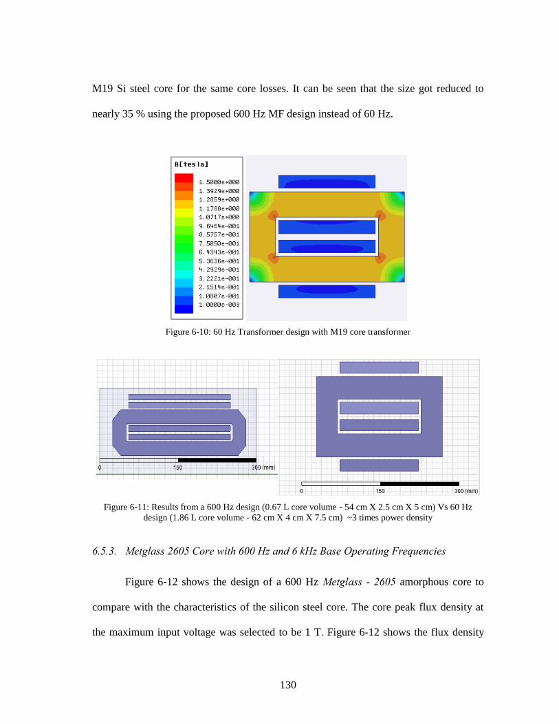
130
M19 Si steel core for the same core losses. It can be seen that the size got reduced to
nearly 35 % using the proposed 600 Hz MF design instead of 60 Hz.
Figure 6-10: 60 Hz Transformer design with M19 core transformer
Figure 6-11: Results from a 600 Hz design (0.67 L core volume - 54 cm X 2.5 cm X 5 cm) Vs 60 Hz
design (1.86 L core volume - 62 cm X 4 cm X 7.5 cm) ~3 times power density
6.5.3. Metglass 2605 Core with 600 Hz and 6 kHz Base Operating Frequencies
Figure 6-12 shows the design of a 600 Hz Metglass - 2605 amorphous core to
compare with the characteristics of the silicon steel core. The core peak flux density at
the maximum input voltage was selected to be 1 T. Figure 6-12 shows the flux density
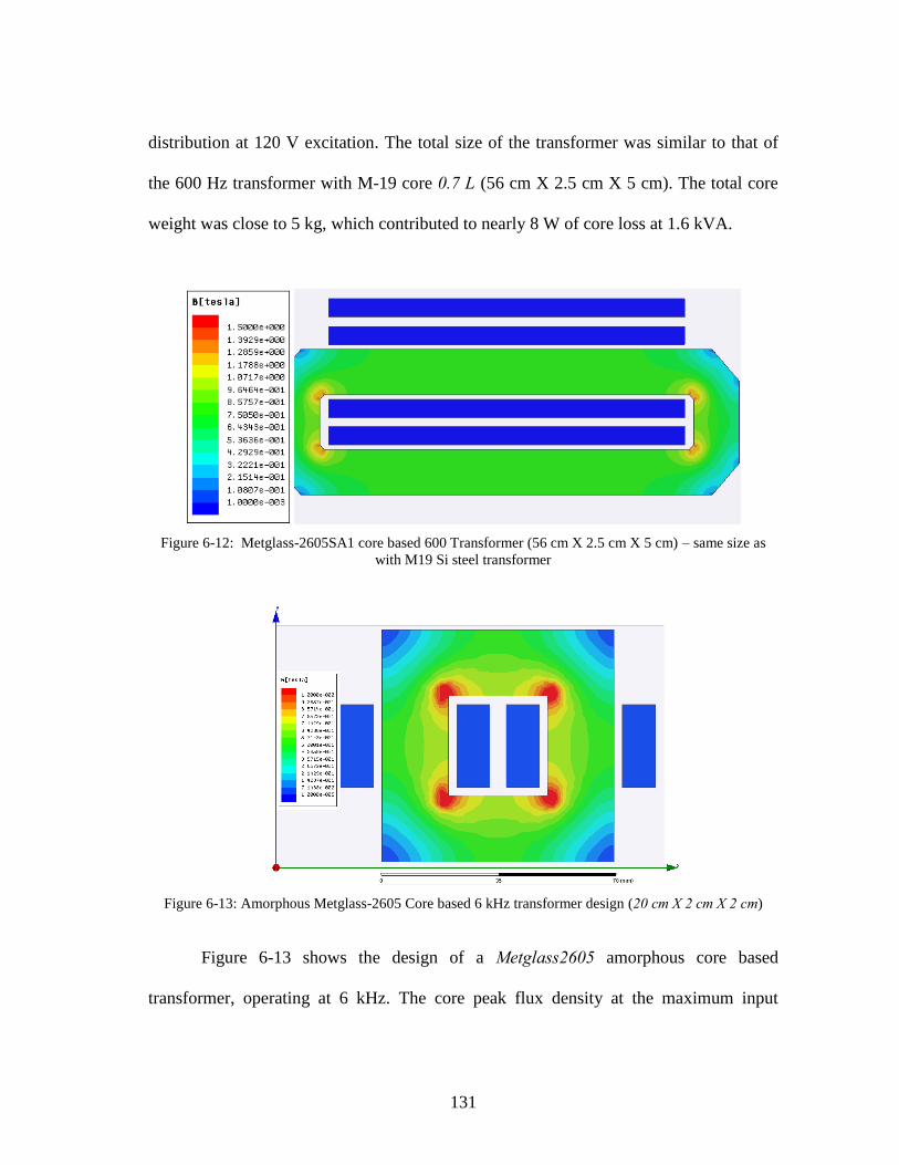
131
distribution at 120 V excitation. The total size of the transformer was similar to that of
the 600 Hz transformer with M-19 core 0.7 L (56 cm X 2.5 cm X 5 cm). The total core
weight was close to 5 kg, which contributed to nearly 8 W of core loss at 1.6 kVA.
Figure 6-12: Metglass-2605SA1 core based 600 Transformer (56 cm X 2.5 cm X 5 cm) – same size as
with M19 Si steel transformer
Figure 6-13: Amorphous Metglass-2605 Core based 6 kHz transformer design (20 cm X 2 cm X 2 cm)
Figure 6-13 shows the design of a Metglass2605 amorphous core based
transformer, operating at 6 kHz. The core peak flux density at the maximum input

132
voltage was designed to be 0.55 T. Figure 6-13 shows the maximum flux density
condition. The total size of the transformer was 0.08 L (20 cm X 2 cm X 2 cm). The total
core weight was close to 0.6 kg, which led to nearly 14 W of core loss at 1.6 kVA.
6.5.4. Ferrite 3C85 Core with 6 kHz Base Operating Frequency
Figure 6-14 shows the alternative 6 kHz transformer design using ferrite 3C85
ferrite core based transformer. The core peak flux density at the maximum input voltage
was designed to be 0.3 T. Figure 6-14 shows the maximum flux density condition. The
total size of the transformer came out to be the same, as discussed before, at 0.08 L (20
cm X 2 cm X 2 cm), but the number of turns was increased to 80 compared to 60 in the
previous design (6 kHz with amorphous core). The total core weight was close to 0.4 kg,
which contributed to nearly 5 W of core loss at 1.6 kVA.
Figure 6-14: Ferrite 3C85 Core based 6 kHz transformer design (20 cm X 2 cm X 2 cm)

133
6.6. Inference and Conclusion
The previous sub-sections discussed the medium frequency (MF) and high
frequency (HF) transformer designs and analysis in detail and simulated the different
designs using Ansys Maxwell software. It could be seen that though the MF transformer
core loss per kg increases significantly while using Si steel core, the total losses of the
transformer can be made to be almost equal to the line frequency design due to the
reduction in the size. Use of amorphous core can significantly reduce the losses even at
MF design. But for operating frequencies between 2 kHz and 5 kHz, the amorphous core
can cause significant audible noise and beyond 5 kHz, the core loss of the amorphous
core itself will become very high, making the core temperature rise also to intolerable
limits. Beyond 5 kHz, ferrite cores seem to be very attractive due to their low loss
characteristics and almost constant permeability over the entire range of operation. But
then the converter losses become higher due to higher switching frequencies.
Table 6-1 summarizes the results and observations from the design and
simulations of the different transformers. It can be seen that using a 600 Hz MF design
with M19 Si steel core can bring the size and the cost of a transformer by one-third
compared to a 60 Hz design with the same material, at the same net transformer losses.
If a Metglass core is used, the size and efficiency of a MF (600 Hz) design can be
brought down to nearly one-third of a 60 Hz transformer design with silicon steel core,
at a similar cost (even including converter costs).
Table 6-1 assumes from Table 1-1 that the normalized cost of winding is almost
40 % the cost of the core for a practical 60 Hz transformer design [15]. The cost of the

134
60 Hz core using M19 (silicon steel) is considered to be 1 p.u. and the other costs are
shown with respect to that. It is assumed that the cost per kg of Metglass 2605 core is
almost 3 times that of M19 core and cost per unit volume of ferrite core is almost twice
that of Metglass 2605 core. Table 6-1 also shows the comparison of 6 kHz operating
frequency based design with the 600 Hz and 60 Hz designs. It can be seen that a HF
transformer constructed with ferrite 3C85 core features to be the best in terms of cost,
efficiency as well as power density, even while operating at 6 kHz. But it should be
noted that for a high power converter system over several hundreds of kilowatts,
operating with hard switching at 6 kHz significantly increases the switching losses,
nullifying the effects of the efficiency, cost and size gains from the usage of ferrite core.
Table 6-1: Summary of transformer design parameters and values discussed earlier in this section
TransformerDesign
M19 Core60 Hz
M19 Core600 Hz
Metglass 600 Hz
Metglass - 26056 kHz
Ferrite - 3C856 kHz
Operating Frequency (Hz) 60 600 600 6000 6000
Max. Flux Density (T) 1.25 0.55 1.1 0.55 0.3
Core Dimensions (cm) 62 X 4 X 7.5 54 X 5 X 2.5 60 X 4.5 X 2.5 20 X 2 X 2 20 X 2 X 2
Number of turns 250 140 180 80 80
Core Volume (L) 1.9 0.67 0.62 0.08 0.08
Core Weight (kg) 14.8 5.3 5.0 0.6 0.4
Core Loss/Mass (W/kg) 1.7 7.5 1.8 24 12
Net Core Loss (W) 25 40 9 14 5
Winding Loss (W) 20 6 8 3 3
Total Transformer Loss (W) 45 46 17 17 8
Efficiency at 1.6 kVA (%) 97.3 97.2 99.0 99.0 99.5
Cost of Core (p.u.) 1.0 0.35 1.0 0.15 0.3
Cost of Winding (p.u.) 0.4 0.13 0.2 0.1 0.1
Total Cost (p.u.) 1.4 0.48 1.2 0.25 0.4
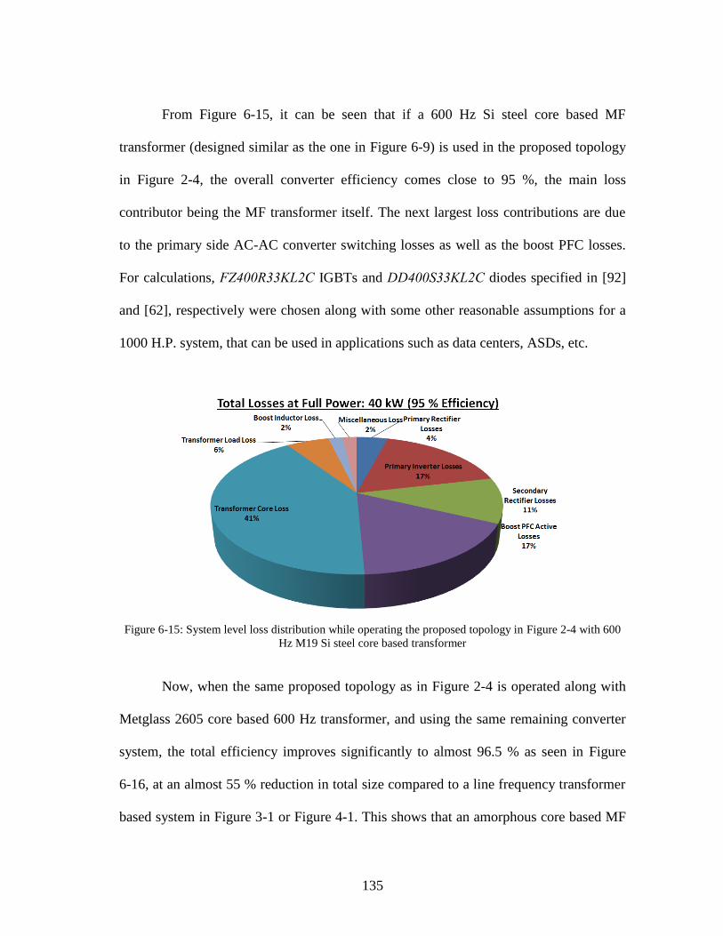
135
From Figure 6-15, it can be seen that if a 600 Hz Si steel core based MF
transformer (designed similar as the one in Figure 6-9) is used in the proposed topology
in Figure 2-4, the overall converter efficiency comes close to 95 %, the main loss
contributor being the MF transformer itself. The next largest loss contributions are due
to the primary side AC-AC converter switching losses as well as the boost PFC losses.
For calculations, FZ400R33KL2C IGBTs and DD400S33KL2C diodes specified in [92]
and [62], respectively were chosen along with some other reasonable assumptions for a
1000 H.P. system, that can be used in applications such as data centers, ASDs, etc.
Figure 6-15: System level loss distribution while operating the proposed topology in Figure 2-4 with 600
Hz M19 Si steel core based transformer
Now, when the same proposed topology as in Figure 2-4 is operated along with
Metglass 2605 core based 600 Hz transformer, and using the same remaining converter
system, the total efficiency improves significantly to almost 96.5 % as seen in Figure
6-16, at an almost 55 % reduction in total size compared to a line frequency transformer
based system in Figure 3-1 or Figure 4-1. This shows that an amorphous core based MF
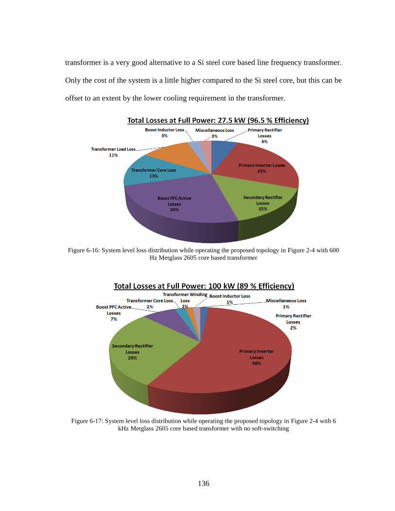
136
transformer is a very good alternative to a Si steel core based line frequency transformer.
Only the cost of the system is a little higher compared to the Si steel core, but this can be
offset to an extent by the lower cooling requirement in the transformer.
Figure 6-16: System level loss distribution while operating the proposed topology in Figure 2-4 with 600
Hz Metglass 2605 core based transformer
Figure 6-17: System level loss distribution while operating the proposed topology in Figure 2-4 with 6
kHz Metglass 2605 core based transformer with no soft-switching

137
In order to have a fair comparison on the total losses in the system for even
higher transformer core frequencies, a similar analysis was performed for a 6 kHz
transformer designed using both amorphous material (Metglass 2605) and ferrite
material (3C85). First, the analysis assumes that no soft-switching is involved in this
application. Since the loss contribution at 6 kHz by both Metglass as well as ferrite core
is low (compared to the remaining system) owing to the small core size and loss
characteristics, only the loss distribution of amorphous core transformer based topology
(in Figure 2-4) is shown in Figure 6-17. In the same system, if soft-switching is
performed to lower the switching losses on the AC-AC converter and the secondary side
diode rectifier, an overall efficiency of 96.5 % as in the previous case (see Figure 6-16)
can be attained only if soft-switching is able to reduce net switching losses to one-fifth,
which is difficult to achieve in a high power system, especially with pulsating DC bus.
Overall for high power isolated converters, a Si steel core - MF transformer
based system fares well in terms of cost and size compared to a 60 Hz design, where as
an amorphous core - MF transformer based system fares well in terms of efficiency and
size compared to a conventional 60 Hz design (with Si steel core), while a ferrite core
can be useful if appropriate soft-switching techniques are identified. Finally the relative
size occupied by various components in the above mentioned transformer as well as
converter designs related to the proposed topology in Figure 2-4 are briefed in Figure
6-18 (considering the overall system size of conventional 60 Hz transformer based
approach is 1 p.u.). While the 60 Hz and 1200 Hz core frequency based designs have
been assumed to operate with hard-switching, the ferrite core (3C85) based system is
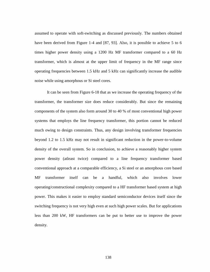
138
assumed to operate with soft-switching as discussed previously. The numbers obtained
have been derived from Figure 1-4 and [87, 93]. Also, it is possible to achieve 5 to 6
times higher power density using a 1200 Hz MF transformer compared to a 60 Hz
transformer, which is almost at the upper limit of frequency in the MF range since
operating frequencies between 1.5 kHz and 5 kHz can significantly increase the audible
noise while using amorphous or Si steel cores.
It can be seen from Figure 6-18 that as we increase the operating frequency of the
transformer, the transformer size does reduce considerably. But since the remaining
components of the system also form around 30 to 40 % of most conventional high power
systems that employs the line frequency transformer, this portion cannot be reduced
much owing to design constraints. Thus, any design involving transformer frequencies
beyond 1.2 to 1.5 kHz may not result in significant reduction in the power-to-volume
density of the overall system. So in conclusion, to achieve a reasonably higher system
power density (atleast twice) compared to a line frequency transformer based
conventional approach at a comparable efficiency, a Si steel or an amorphous core based
MF transformer itself can be a handful, which also involves lower
operating/constructional complexity compared to a HF transformer based system at high
power. This makes it easier to employ standard semiconductor devices itself since the
switching frequency is not very high even at such high power scales. But for applications
less than 200 kW, HF transformers can be put to better use to improve the power
density.
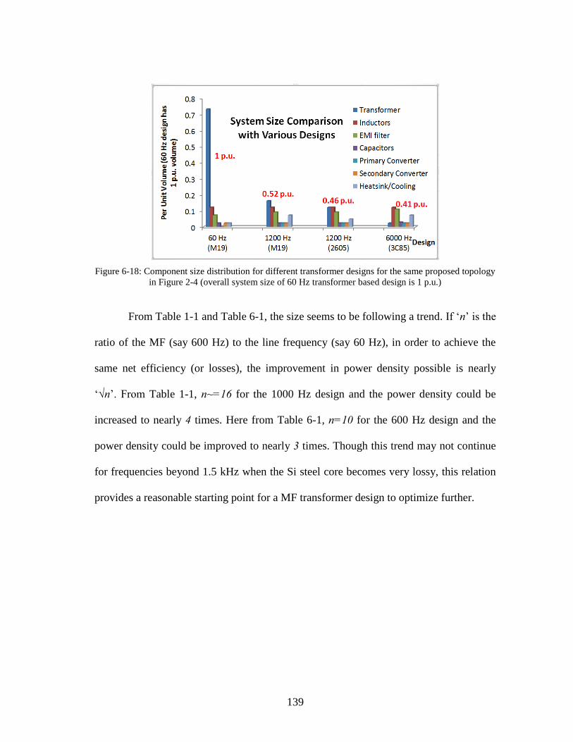
139
Figure 6-18: Component size distribution for different transformer designs for the same proposed topology
in Figure 2-4 (overall system size of 60 Hz transformer based design is 1 p.u.)
From Table 1-1 and Table 6-1, the size seems to be following a trend. If ‘n’ is the
ratio of the MF (say 600 Hz) to the line frequency (say 60 Hz), in order to achieve the
same net efficiency (or losses), the improvement in power density possible is nearly
‘√n’. From Table 1-1, n~=16 for the 1000 Hz design and the power density could be
increased to nearly 4 times. Here from Table 6-1, n=10 for the 600 Hz design and the
power density could be improved to nearly 3 times. Though this trend may not continue
for frequencies beyond 1.5 kHz when the Si steel core becomes very lossy, this relation
provides a reasonable starting point for a MF transformer design to optimize further.

140
7. SUMMARY
7.1. Conclusion
This dissertation first introduced various utility interface applications and the
concepts of power density in converters. Then the section discussed the mathematical
modeling of power converters at various modulation schemes along with some of the
basic ways of implementing the models using AC-AC converters.
The subsequent section proposed an isolated 3-phase AC-DC converter using MF
or HF transformers, which can be used for various applications such as in telecom power
supplies, battery charging, etc. The design and control strategy were explained in detail
and the concepts were validated through simulations and experiments. Section 3
proposed a simplified multi-pulse diode rectifier concept using MF or HF transformers
that replace bulky line frequency transformers from a typical system. The theory and
design of the conventional systems were presented followed by the explanation of the
proposed approach. Detailed analysis, simulation and experiments were performed for a
12-pulse rectifier configuration, and ways to extend this concept to higher configurations
were also discussed.
Section 4 extended some of the concepts proposed in section 2 and applied them
to develop topologies for wind turbine generator (WTG) – medium voltage DC (MVDC)
interconnection suitable for offshore farms and long-distance transmission line. The
section started with the introduction to offshore wind farms and some of the WTG –
MVDC converters already proposed in the literature. After explaining the theory and

141
operation of the proposed topology, simulation results were shown which demonstrated
the control mechanism and robustness of the system. The subsequent section introduced
the importance of battery energy storage systems (BESS) in modern day grid and
discussed some of the power electronic topologies that have been proposed in the
literature to interface large BESS systems with the utility grid. Then a MF transformer
based approach was proposed for interfacing a large scale BESS system to the utility
grid. As an extension, a 3-port scheme for interfacing a WTG system along with a BESS
system was also introduced in this section. Detailed simulation and experimental results
were shown. Salient features of a large wind farm, such as low voltage ride through
(LVRT), fault-handling capacity, etc. were also discussed in detail.
Section 6 concentrated on the design and modeling the MF/HF transformers
using ANSYS Maxwell software. Transformers designed at different core frequencies
using various materials such as silicon steel, amorphous, ferrite, etc. were evaluated in
depth under the criteria of size and losses. Comparison in terms of size and losses in the
MF or HF transformers with respect to the line frequency transformer was also shown.
The best designs with regards to different parameters of size, cost and efficiency were
noted; and a relative component size study was performed for the overall converter.
To conclude, this dissertation proposed several approaches using which it is
possible to replace bulky line frequency transformers with medium or high frequency
‘solid-state transformers’ and avoid large DC electrolytic capacitors to improve the
power density as well as reduce the cost of typical medium and high power applications
such as ASDs, WTGs, etc. It was identified that for such systems, MF transformers

142
constructed using electrical steel or amorphous cores could significantly reduce the
overall system size to almost 40 %, with potential to further improvement in size and
efficiency. For such high power applications, though it is possible to opt for an even
higher frequency transformer core such as ferrite or nano-crystalline, this may lead to
higher switching losses in the power converters and will significantly reduce the ‘fill
factor’ of the windings due to the corona losses beyond certain frequencies, resulting in a
lower efficiency at only a meagre improvement in power density. Medium frequency
transformers can be very suitable for such situations leading to higher power density,
either at a lower cost or higher efficiency.
7.2. Future Work
Various other possibilities arise from this dissertation. A few are listed below:
Soft-switching techniques that can be employed at even higher switching frequencies
in the proposed topologies; also resonant energy conversion can be studied.
Though the experiments in this dissertation regarding multi-pulse rectifier were on
12-pulse topology, 18-pulse and higher configurations can be constructed and tested
on an even larger scale.
Since only the 600 Hz Si steel transformer was constructed and tested, all the other
transformers designed and simulated in the earlier section can also be constructed
and tested on laboratory prototypes.
Nano-crystalline core based transformers can be investigated for higher operating
frequencies and in situations where high temperature operation is desired.
143
REFERENCES
[1] T. Mai;, R. Wiser;, D. Sandor;, G. Brinkman;, G. Heath;, P. Denholm;, D. J.
Hostick;, N. Darghouth;, A. Schlosser;, and K. Strzepek;. (Nov. 30, 2014).
"Renewable Electricity Futures Study" (Volume 1 ed.). Available:
http://www.nrel.gov/docs/fy12osti/52409-1.pdf
[2] H. S. Krishnamoorthy, S. Essakiappan, P. N. Enjeti, R. S. Balog, and S. Ahmed,
"A new multilevel converter for megawatt scale solar photovoltaic utility
integration," in Twenty-Seventh Annual IEEE Applied Power Electronics Conference and Exposition (APEC), 2012, pp. 1431-1438.
[3] M. Charles. (Nov. 30, 2014). "California’s Energy Storage Mandate: Electricity Advisory Committee Meeting". Available:
http://energy.gov/sites/prod/files/2014/06/f17/EACJune2014-3Charles.pdf
[4] W. Kramer;, S. Chakraborty;, B. Kroposki;, and H. Thomas;. (Nov. 30, 2014).
"Advanced Power Electronic Interfaces for Distributed Energy Systems".
Available: http://www.nrel.gov/docs/fy08osti/42672.pdf
[5] ABB. (Nov 30 2014). "A world in transformation". Available:
http://www05.abb.com/global/scot/scot271.nsf/veritydisplay/c3791bac5b25bd10
c1257ab80037553b/$file/ABB%20SR%20Transformers-121031.pdf
[6] F. Blaabjerg, A. Consoli, J. A. Ferreira, and J. D. Van Wyk, "The future of
electronic power processing and conversion," Industry Applications, IEEE Transactions on, vol. 41, pp. 3-8, 2005.
[7] R. Burkart and J. W. Kolar, "Component cost models for multi-objective
optimizations of switched-mode power converters," in Energy Conversion Congress and Exposition (ECCE), 2013 IEEE, 2013, pp. 2139-2146.
[8] A. Rufer, N. Schibli, C. Chabert, and C. Zimmermann, "Configurable front-end
converters for multicurrent locomotives operated on 16 2/3 Hz AC and 3 kV DC
systems," Power Electronics, IEEE Transactions on, vol. 18, pp. 1186-1193,
2003.
[9] Railway-Technical. (Nov. 30, 2014). "Electric Locomotives". Available:
http://www.railway-technical.com/elec-loco-bloc.shtml
144
[10] R. Raju. (Nov. 30, 2014). "Silicon Carbide: High Voltage, High Frequency Conversion" [NIST High Megawatt Variable Speed Drive Technology
Workshop]. Available:
http://www.nist.gov/pml/high_megawatt/upload/Approved-Raju-
DoE_NIST_HMW_VSD_GE_raju.pdf
[11] R. M. Burkart and J. W. Kolar, "Comparative evaluation of SiC and Si PV
inverter systems based on power density and efficiency as indicators of initial
cost and operating revenue," in Control and Modeling for Power Electronics (COMPEL), 2013 IEEE 14th Workshop on, 2013, pp. 1-6.
[12] J. W. Kolar; and G. I. Ortiz;. (Nov. 30 2014). "Solid State Transformer Concepts in Traction and Smart Grid Applications". Available:
https://www.pes.ee.ethz.ch/uploads/tx_ethpublications/__ECCE_Europe_SST_T
utorial_FINAL_as_corrected___extended_after_ECCE_12_130912.pdf
[13] L. Chun-kit, S. Dutta, B. Seunghun, and S. Bhattacharya, "Design considerations
of high voltage and high frequency three phase transformer for Solid State
Transformer application," in Energy Conversion Congress and Exposition (ECCE), 2010 IEEE, 2010, pp. 1551-1558.
[14] G. Ortiz, J. Biela, and J. W. Kolar, "Optimized design of medium frequency
transformers with high isolation requirements," in IECON 2010 - 36th Annual Conference on IEEE Industrial Electronics Society, 2010, pp. 631-638.
[15] Alibaba. (Nov. 30 2014). "Grain-Oriented Silicon Sheets". Available:
http://www.alibaba.com/showroom/grain-oriented-silicon-steel-sheet.html
[16] T. Soeiro, T. Friedli, and J. W. Kolar, "Three-phase high power factor mains
interface concepts for Electric Vehicle battery charging systems," in Twenty-Seventh Annual IEEE Applied Power Electronics Conference and Exposition (APEC), 2012, pp. 2603-2610.
[17] H. Akagi and K. Isozaki, "A Hybrid Active Filter for a Three-Phase 12-Pulse
Diode Rectifier Used as the Front End of a Medium-Voltage Motor Drive,"
Power Electronics, IEEE Transactions on, vol. 27, pp. 69-77, 2012.
[18] B. N. Singh, P. Jain, and G. Joos, "Three-phase AC/DC regulated power
supplies: a comparative evaluation of different topologies," in Applied Power Electronics Conference and Exposition, 2000. APEC 2000. Fifteenth Annual IEEE, 2000, pp. 513-518 vol.1.
145
[19] G. Spiazzi and F. C. Lee, "Implementation of single-phase boost power-factor-
correction circuits in three-phase applications," Industrial Electronics, IEEE Transactions on, vol. 44, pp. 365-371, 1997.
[20] P. Drabek, Z. Peroutka, M. Pittermann, Ce, x, and M. dl, "New Configuration of
Traction Converter With Medium-Frequency Transformer Using Matrix
Converters," Industrial Electronics, IEEE Transactions on, vol. 58, pp. 5041-
5048, 2011.
[21] P. Barbosa, F. Canales, and F. C. Lee, "A front-end distributed power system for
high-power applications," in Industry Applications Conference, 2000. Conference Record of the 2000 IEEE, 2000, pp. 2546-2551 vol.4.
[22] J. W. Kolar; et. al., "Three-Phase PFC Rectifier and AC-AC Converter Systems,"
in Applie Power Electronics Conference (APEC), TX, 2011.
[23] J. W. Kolar; G. Ortiz, "Solid-State-Transformers: Key Components of Future
Traction and Smart Grid Systems," in International Power Electronics Conference - ECCE Asia (IPEC), Hiroshima, Japan, 2014.
[24] T. Friedli, M. Hartmann, and J. W. Kolar, "The Essence of Three-Phase PFC
Rectifier Systems-Part II," Power Electronics, IEEE Transactions on, vol. 29, pp.
543-560, 2014.
[25] J. W. Kolar and T. Friedli, "The Essence of Three-Phase PFC Rectifier Systems-
Part I," Power Electronics, IEEE Transactions on, vol. 28, pp. 176-198, 2013.
[26] B. Hafez, H. S. Krishnamoorthy, P. Enjeti, S. Ahmed, and I. J. Pitel, "Medium
voltage power distribution architecture with medium frequency isolation
transformer for data centers," in Applied Power Electronics Conference and Exposition (APEC), 2014 Twenty-Ninth Annual IEEE, 2014, pp. 3485-3489.
[27] H. S. Krishnamoorthy, D. Rana, P. Garg, P. N. Enjeti, and I. J. Pitel, "Wind
Turbine Generator - Battery Energy Storage Utility Interface Converter Topology
With Medium-Frequency Transformer Link," Power Electronics, IEEE Transactions on, vol. 29, pp. 4146-4155, 2014.
[28] H. S. Krishnamoorthy, P. Garg, and P. N. Enjeti, "A matrix converter-based
topology for high power electric vehicle battery charging and V2G application,"
in 38th Annual Conference on IEEE Industrial Electronics Society, 2012, pp.
2866-2871.
146
[29] C. Citro, A. Luna, J. Rocabert, R. S. Munoz-Aguilar, I. Candela, and P.
Rodriguez, "Overview of power processing structures for embedding Energy
Storage in PV power converters," in IECON 2011 - 37th Annual Conference on IEEE Industrial Electronics Society, 2011, pp. 2492-2498.
[30] M. Hartmann, J. Miniboeck, H. Ertl, and J. W. Kolar, "A Three-Phase Delta
Switch Rectifier for Use in Modern Aircraft," Industrial Electronics, IEEE Transactions on, vol. 59, pp. 3635-3647, 2012.
[31] C. Yong-Won, K. Jung-Min, and K. Bong-Hwan, "Single Power-Conversion
AC--DC Converter With High Power Factor and High Efficiency," Power Electronics, IEEE Transactions on, vol. 29, pp. 4797-4806, 2014.
[32] M. Narimani and G. Moschopoulos, "A New Interleaved Three-Phase Single-
Stage PFC AC-DC Converter," Industrial Electronics, IEEE Transactions on, vol. 61, pp. 648-654, 2014.
[33] K. Ho-Sung, B. Ju-Won, R. Myung-Hyu, K. Jong-Hyun, and J. Jee-Hoon, "The
High-Efficiency Isolated AC-DC Converter Using the Three-Phase Interleaved
LLC Resonant Converter Employing the Y-Connected Rectifier," Power Electronics, IEEE Transactions on, vol. 29, pp. 4017-4028, 2014.
[34] B. Tamyurek and D. A. Torrey, "A Three-Phase Unity Power Factor Single-
Stage AC-DC Converter Based on an Interleaved Flyback Topology," Power Electronics, IEEE Transactions on, vol. 26, pp. 308-318, 2011.
[35] B. Tamyurek, "A High-Performance SPWM Controller for Three-Phase UPS
Systems Operating Under Highly Nonlinear Loads," Power Electronics, IEEE Transactions on, vol. 28, pp. 3689-3701, 2013.
[36] S. Norrga, S. Meier, and S. Ostlund, "A Three-Phase Soft-Switched Isolated
AC/DC Converter Without Auxiliary Circuit," Industry Applications, IEEE Transactions on, vol. 44, pp. 836-844, 2008.
[37] J. Everts, F. Krismer, J. Van den Keybus, J. Driesen, and J. W. Kolar, "Optimal
ZVS Modulation of Single-Phase Single-Stage Bidirectional DAB AC-DC
Converters," Power Electronics, IEEE Transactions on, vol. 29, pp. 3954-3970,
2014.
147
[38] H. Byung-Moon, C. Nam-Sup, and L. Jun-Young, "New Bidirectional Intelligent
Semiconductor Transformer for Smart Grid Application," Power Electronics, IEEE Transactions on, vol. 29, pp. 4058-4066, 2014.
[39] H. S. Krishnamoorthy, P. Garg, P. J. Kunwor, and P. N. Enjeti, "3-Phase AC-DC
converter topologies with higher frequency transformer isolation for utility grid
interface," in Applied Power Electronics Conference and Exposition (APEC), 2014 Twenty-Ninth Annual IEEE, 2014, pp. 1240-1247.
[40] G. Bin, J. Dominic, C. BaiFeng, and L. Jih-Sheng, "A high-efficiency single-
phase bidirectional AC-DC converter with miniminized common mode voltages
for battery energy storage systems," in Energy Conversion Congress and Exposition (ECCE), 2013 IEEE, 2013, pp. 5145-5149.
[41] M. R. Islam, G. Youguang, and Z. Jianguo, "A High-Frequency Link Multilevel
Cascaded Medium-Voltage Converter for Direct Grid Integration of Renewable
Energy Systems," Power Electronics, IEEE Transactions on, vol. 29, pp. 4167-
4182, 2014.
[42] M. Swamy and T. Kume, "Present state and a futuristic vision of motor drive
technology," in Optimization of Electrical and Electronic Equipment, 2008. OPTIM 2008. 11th International Conference on, 2008, pp. XLV-LVI.
[43] S. Inoue and H. Akagi, "A Bi-directional isolated DC/DC converter as a core
circuit of the next-generation medium-voltage power conversion system," in 37th IEEE Power Electronics Specialists Conference, 2006, pp. 1-7.
[44] D. A. Rendusara, E. Cengelci, P. N. Enjeti, V. R. Stefanovic, and J. W. Gray,
"Analysis of Common Mode Voltage - "Neutral Shift" in Medium Voltage PWM
Adjustable Speed Drive (MV-ASD) Systems," IEEE Transactions on Power Electronics, vol. 15, pp. 1124-1133, 2000.
[45] S. Jianjiang, G. Wei, Y. Hao, Z. Tiefu, and A. Q. Huang, "Research on Voltage
and Power Balance Control for Cascaded Modular Solid-state Transformer,"
IEEE Transactions on Power Electronics, vol. 26, pp. 1154-1166, 2011.
[46] Z. Tiefu, Y. Liyu, W. Jun, and A. Q. Huang, "270 kVA Solid State Transformer
Based on 10 kV SiC Power Devices," in Electric Ship Technologies Symposium, 2007. ESTS '07. IEEE, 2007, pp. 145-149.
148
[47] M. K. Das, C. Capell, D. E. Grider, R. Raju, M. Schutten, J. Nasadoski, S. Leslie,
J. Ostop, and A. Hefner, "10 kV, 120 A SiC half H-bridge power MOSFET
modules suitable for high frequency, medium voltage applications," in Energy Conversion Congress and Exposition (ECCE), 2011 IEEE, 2011, pp. 2689-2692.
[48] ABB. (Nov. 30, 2014). "Powering the world economy: Is there a better way to use electricity?". Available:
http://www04.abb.com/global/seitp/seitp202.nsf/0/ec96823a06519347c12578b50
0362974/$file/ABB_ElectricMotors_infographic.pdf
[49] ABB. (2011, Nov. 30, 2014). "Chemical, Oil and Gas: Medium voltage drives for greater profitability and performance". Available:
http://www05.abb.com/global/scot/scot216.nsf/veritydisplay/7afdc73aa9256670c
12578b5004a2ae5/$file/cog%20brochure%20revc_lowres.pdf
[50] E. Hydraulic Institute, DOE. (2004, 11/26). Variable speed pumping. Available:
http://www1.eere.energy.gov/manufacturing/tech_assistance/pdfs/variable_speed
_pumping.pdf
[51] G. Gong, U. Drofenik, and J. W. Kolar, "12-pulse rectifier for more electric
aircraft applications," in Industrial Technology, 2003 IEEE International Conference on, 2003, pp. 1096-1101 Vol.2.
[52] Siemens. (Nov. 30, 2014). "Robicon VFDs: Perfect Harmony". Available:
http://eastcoastmotor.com/wordpress/wp-content/uploads/2013/04/robicon-
perfect-harmony-short-overview.pdf
[53] H. S. Krishnamoorthy, P. N. Enjeti, I. J. Pitel, and J. T. Hawke, "New medium-
voltage Adjustable Speed Drive (ASD) topologies with medium-frequency
transformer isolation," in Power Electronics and Motion Control Conference (IPEMC), 2012 7th International, 2012, pp. 814-819.
[54] ABB. (Nov. 30, 2014). "Medium Voltage AC Drives: ACS 5000 Series".
Available:
http://www05.abb.com/global/scot/scot216.nsf/veritydisplay/8971bcb62448dd5d
c1257b160053775b/$file/ACS%205000%20EN%20Rev%20H_lowres.pdf
[55] M. H. Rashid, "POWER ELECTRONICS HANDBOOK": Academic Press, 2001.
[56] D. Wensky, "FACTS and HVDC for grid connection of large offshore wind
farms."
149
[57] A.-K. Skytt, P. Holmberg, and L.-E. Juhlin, "HVDC Light for connection of
wind farms," in Second International Workshop on Transmission Networks for Offshore Wind Farms Royal Institute of Technology Stockholm, Sweden, 2001.
[58] L. Harnefors, Y. Jiang-Häfner, M. Hyttinen, and T. Jonsson, "Ride-through
methods for wind farms connected to the grid via a VSC-HVDC transmission,"
2007.
[59] P. Jones, B. Westman, C. Plant, and M. Foster, "From generation to grid,"
Renewable Energy Focus, vol. 8, pp. 38-42, 2007.
[60] E. V. Larsen and R. W. Delmerico, "Hvdc connection of wind turbine," ed:
Google Patents, 2011.
[61] T. M. CLARE JONATHAN CHARLES, ; TRAINER DAVID, ; WHITEHOUSE
ROBERT, ""HYBRID 2-LEVEL AND MULTILEVEL HVDC
CONVERTER"."
[62] Infineon. (Nov. 30, 2014). "DD400S33KL2C: Technical Datasheet". Available:
http://www.infineon.com/dgdl/Infineon-DD400S33KL2C-DS-v02_00-
en_cn.pdf?fileId=db3a30433e20bc87013e20c67d6c0001
[63] Z. Jindong, M. M. Jovanovic, and F. C. Lee, "Comparison between CCM single-
stage and two-stage boost PFC converters," in Applied Power Electronics Conference and Exposition, 1999. APEC '99. Fourteenth Annual, 1999, pp. 335-
341 vol.1.
[64] ABB. (Nov 30 2014). "ABB Boderline". Available:
http://www05.abb.com/global/scot/scot271.nsf/veritydisplay/febcd9def08a98dbc
12575e4004a0f2f/$file/35-41%202m967_eng72dpi.pdf
[65] H. Polinder, D. Bang, R. P. J. O. M. van Rooij, A. S. McDonald, and M. A.
Mueller, "10 MW Wind Turbine Direct-Drive Generator Design with Pitch or
Active Speed Stall Control," in Electric Machines & Drives Conference, 2007. IEMDC '07. IEEE International, 2007, pp. 1390-1395.
[66] J. S. Thongam; and M. Ouhrouche;. (Nov. 30 2014). "MPPT Control Methods in Wind Energy Conversion Systems". Available:
http://www.intechopen.com/books/fundamental-and-advanced-topics-in-wind-
power/mppt-control-methods-in-wind-energy-conversion-systems
150
[67] L. Maharjan, S. Inoue, H. Akagi, and J. Asakura, "A transformerless battery
energy storage system based on a multilevel cascade PWM converter," in 2008 IEEE Power Electronics Specialists Conference, 2008, pp. 4798-4804.
[68] P. F. Ribeiro, B. K. Johnson, M. L. Crow, A. Arsoy, and Y. Liu, "Energy storage
systems for advanced power applications," Proceedings of the IEEE, vol. 89, pp.
1744-1756, 2001.
[69] S. Sharma and B. Singh, "Performance of Voltage and Frequency Controller in
Isolated Wind Power Generation for a Three-Phase Four-Wire System," Power Electronics, IEEE Transactions on, vol. 26, pp. 3443-3452, 2011.
[70] X. Zhuang, L. Rui, Z. Hui, X. Dianguo, and C. H. Zhang, "Control of Parallel
Multiple Converters for Direct-Drive Permanent-Magnet Wind Power
Generation Systems," Power Electronics, IEEE Transactions on, vol. 27, pp.
1259-1270, 2012.
[71] ABB. (Nov. 30 2014). "DES Distributed Energy Storage modules Up to 2MW".
Available:
http://www05.abb.com/global/scot/scot235.nsf/veritydisplay/209ba3fbd42472a6c
1257b130057436f/$file/des_brochure.pdf
[72] N. W. Miller, R. S. Zrebiec, G. Hunt, and R. W. Deimerico, "Design and
commissioning of a 5 MVA, 2.5 MWh battery energy storage system," in
Transmission and Distribution Conference, 1996. Proceedings., 1996 IEEE,
1996, pp. 339-345.
[73] S. Thomas, M. Stieneker, and R. W. De Doncker, "Development of a modular
high-power converter system for battery energy storage systems," in Power Electronics and Applications (EPE 2011), Proceedings of the 2011-14th European Conference on, 2011, pp. 1-10.
[74] L. H. Walker, "10 MW GTO converter for battery peaking service," in Industry Applications Society Annual Meeting, 1988., Conference Record of the 1988 IEEE, 1988, pp. 850-858 vol.1.
[75] J. P. Barranger, Hysteresis and eddy-current losses of a transformer lamination viewed as an application of the Poynting theorem: National Aeronautics and
Space Administration, 1965.
151
[76] D. E. Consultancy. (Nov. 30 2014). "Best Practice Manual for Electric Transformers”. Available:
http://www.energymanagertraining.com/bee_draft_codes/best_practices_manual-
TRANSFORMERS.pdf
[77] Q. Hengsi and J. W. Kimball, "Solid-State Transformer Architecture Using
AC–AC Dual-Active-Bridge Converter," Industrial Electronics, IEEE Transactions on, vol. 60, pp. 3720-3730, 2013.
[78] T. Zhao, G. Wang, S. Bhattacharya, and A. Q. Huang, "Voltage and Power
Balance Control for a Cascaded H-Bridge Converter-Based Solid-State
Transformer," Power Electronics, IEEE Transactions on, vol. 28, pp. 1523-1532,
2013.
[79] S. Deshang, X. Guo, and L. Xiaozhong, "Control Strategy for Input-Series-
Output-Series High-Frequency AC-Link Inverters," Power Electronics, IEEE Transactions on, vol. 28, pp. 5283-5292, 2013.
[80] H. S. Krishnamoorthy, P. Garg, and P. N. Enjeti, "A new medium-voltage energy
storage converter topology with medium-frequency transformer isolation," in
Energy Conversion Congress and Exposition (ECCE), 2012 IEEE, 2012, pp.
3471-3478.
[81] P. R. Tenca, A. A.; Lipo, T. A. (2007, 11/26). LVRT Capability for Wind Turbines based on Current Source Inverter Topologies. Available:
http://lipo.ece.wisc.edu/2007pubs/2007_34.pdf
[82] K. Ki-Hong, J. Yoon-Cheul, L. Dong-Choon, and K. Heung-Geun, "LVRT
Scheme of PMSG Wind Power Systems Based on Feedback Linearization,"
Power Electronics, IEEE Transactions on, vol. 27, pp. 2376-2384, 2012.
[83] T. Senjyu, N. Nakasone, A. Yona, A. Y. Saber, T. Funabashi, and H. Sekine,
"Operation strategies for stability of gearless wind power generation systems," in
Power and Energy Society General Meeting - Conversion and Delivery of Electrical Energy in the 21st Century, 2008 IEEE, 2008, pp. 1-7.
[84] A. V. d. Bossche; and V. C. Valchev;. (Nov 30 2014). "Inductors and Transformersfor Power Electronics". Available: http://192.211.49.220/-
%20Electronics/Books/Inductors%20And%20Transformers%20For%20Power%
20Electronics.pdf

152
[85] W. books. (Nov 30 2014). "Transformer Design". Available:
http://en.wikibooks.org/wiki/Electronics/Transformer_Design
[86] C. W. T. McLyman, Transformer and Inductor Design Handbook, Third Edition:
Taylor & Francis, 2004.
[87] J. Biela and J. W. Kolar, "Cooling Concepts for High Power Density Magnetic
Devices," in Power Conversion Conference - Nagoya, 2007. PCC '07, 2007, pp.
1-8.
[88] Metglas. (Nov 30 2014). "Metglas® 2605SA1 & 2605HB1M Magnetic Alloy".
Available: http://www.metglas.com/products/magnetic_materials/2605sa1.asp
[89] Philips. (Nov 30 2014). "Magnetic Products-Data Sheet". Available:
http://www.thierry-lequeu.fr/data/3C85.pdf
[90] C. W. T. McLyman. (Nov 30 2014). "Window Utilization Factor". Available:
http://www.kgmagnetics.org/APNOTES-06/An-102.pdf
[91] E. Colarado. (Nov. 30 2014). "Inductor Design". Available:
http://ecee.colorado.edu/~ecen5797/course_material/Ch14slides.pdf
[92] Infineon. (Nov. 30, 2014). "FZ400R33KL2C: Technical Datasheet". Available:
http://www.infineon.com/dgdl/Infineon-FZ400R33KL2C_B5-DS-v02_00-
en_cn.pdf?fileId=db3a30433e16edf9013e184ae5870336
[93] J. Biela, U. Badstuebner, and J. W. Kolar, "Impact of Power Density
Maximization on Efficiency of DC–DC Converter Systems," Power Electronics, IEEE Transactions on, vol. 24, pp. 288-300, 2009.


