Embed Size (px)
Citation preview

www.infineon.com
Please note that Cypress is an Infineon Technologies Company.The document following this cover page is marked as “Cypress” document as this is the company that originally developed the product. Please note that Infineon will continue to offer the product to new and existing customers as part of the Infineon product portfolio.
Continuity of document contentThe fact that Infineon offers the following product as part of the Infineon product portfolio does not lead to any changes to this document. Future revisions will occur when appropriate, and any changes will be set out on the document history page.
Continuity of ordering part numbersInfineon continues to support existing part numbers. Please continue to use the ordering part numbers listed in the datasheet for ordering.

The following document contains information on Cypress products. The document has the series name, product name, and ordering part numbering with the prefix “MB”. However, Cypress will offer these products to new and existing customers with the series name, product name, and ordering part number with the prefix “CY”. How to Check the Ordering Part Number 1. Go to www.cypress.com/pcn. 2. Enter the keyword (for example, ordering part number) in the SEARCH PCNS field and click
Apply. 3. Click the corresponding title from the search results. 4. Download the Affected Parts List file, which has details of all changes For More Information Please contact your local sales office for additional information about Cypress products and solutions. About Cypress Cypress is the leader in advanced embedded system solutions for the world's most innovative automotive, industrial, smart home appliances, consumer electronics and medical products. Cypress' microcontrollers, analog ICs, wireless and USB-based connectivity solutions and reliable, high-performance memories help engineers design differentiated products and get them to market first. Cypress is committed to providing customers with the best support and development resources on the planet enabling them to disrupt markets by creating new product categories in record time. To learn more, go to www.cypress.com.
MB90350E Series
F2MC-16LX16-bit Microcontrollers
Cypress Semiconductor Corporation • 198 Champion Court • San Jose, CA 95134-1709 • 408-943-2600Document Number: 002-04493 Rev. *A Revised April 7, 2016
The MB90350E series, loaded 1 channel FULL-CAN* interface and Flash ROM, is general-purpose Cypress 16-bit microcontroller designing for automotive and industrial applications. Its main feature is the on-board CAN interface, which conforms to CAN standard Version2.0 Part A and Part B, while supporting a very flexible message buffer scheme and so offering more functions than a normal full CAN approach.
The power supply (3 V) is supplied to the MCU core from an internal regulator circuit. This creates a major advantage in terms of EMI and power consumption.
The PLL clock multiplication circuit provides an internal 42 ns instruction execution time from an external 4 MHz clock. Also, the clock supervisor function can monitor main clock and sub clock independently.
As the peripheral resources, the unit features a 4-channel Output Compare Unit, 6-channel Input Capture Unit, 2 separate 16-bit free-run timers, 2-channel LIN-UART and 15-channel 8/10-bit A/D converter built-in.
: Controller Area Network (CAN) - License of Robert Bosch GmbH
Features
Clock
■ Built-in PLL clock frequency multiplication circuit
■ Selection of machine clocks (PLL clocks) is allowed among frequency division by two on oscillation clock, and multipli-cation of 1 to 6 times of oscillation clock (for 4 MHz oscillation clock, 4 MHz to 24 MHz).
■ Operation by sub clock (up to 50 kHz : 100 kHz oscillation clock divided by two) is allowed (devices without S-suffix only) .
■ Minimum execution time of instruction : 42 ns (when operating with 4-MHz oscillation clock, and 6-timemultiplied PLL clock).
■ Built-in clock modulation circuit
16 Mbytes CPU memory space24-bit internal addressing
Instruction system best suited to controller
■ Wide choice of data types (bit, byte, word, and long word)
■ Wide choice of addressing modes (23 types)
■ Enhanced multiply-divide instructions with sign and RETI instructions
Clock supervisor (MB90x356x and MB90x357xonly) Main clock or sub clock is monitored independently.
Enhanced high-precision computing with 32-bitaccumulator
Instruction system compatible with high-levellanguage (C language) and multitask
■ Employing system stack pointer
■ Enhanced various pointer indirect instructions
■ Barrel shift instructions
Increased processing speed4-byte instruction queue
Powerful interrupt function
■ Powerful 8-level, 34-condition interrupt feature
■ Up to 8 channels external interrupts are supported.
Automatic data transfer function independent ofCPU
■ Extended intelligent I/O service function (EI2OS): up to 16 channels
■ DMA: up to 16 channels
Low power consumption (standby) mode
■ Sleep mode (a mode that stops CPU operating clock)
■ Main timer mode (a timebase timer mode switched from the main clock mode)
■ PLL timer mode (a timebase timer mode switched from the PLL clock mode)
■ Watch mode (a mode that operates sub clock and watch timer only)
■ Stop mode (a mode that stops oscillation clock and sub clock)
■ CPU intermittent operation mode
ProcessCMOS technology
I/O port
■ General-purpose input/output port (CMOS output)49 ports (devices without S-suffix : devices that correspond to sub clock)51 ports (devices with S-suffix : devices that do not correspond to sub clock)
Sub clock pin (X0A, X1A)
■ Yes (using the external oscillation) : devices without S-suffix
■ No (using the sub clock mode at internal CR oscillation) : devices with S-suffix
Timer
■ Timebase timer, watch timer, watchdog timer : 1 channel
MB90350E Series
Document Number: 002-04493 Rev. *A Page 2 of 84
■ 8/16-bit PPG timer : 8-bit 10 channels or 16-bit 6 channels
■ 16-bit reload timer : 2 channels (only Evaluation products has 4 channels)
■ 16- bit input/output timer- 16-bit free-run timer : 2 channels (FRT0 : ICU0/1, FRT1 : ICU4/5/6/7, OCU4/5/6/7)- 16- bit input capture: (ICU) : 6 channels- 16-bit output compare : (OCU) : 4 channels
FULL-CAN interface: 1 channel
■ Compliant with CAN standard Version2.0 Part A and Part B
■ 16 message buffers are built-in
■ CAN wake-up function
LIN-UART: 2 channels
■ Equipped with full-duplex double buffer
■ Clock-asynchronous or clock-synchronous serial transmission is available.
I2C interface: 1 channelUp to 400 kbps transfer rate
DTP/External interrupt: 8 channels, CANwakeup: 1 channelModule for activation of extended intelligent I/O service (EI2OS),DMA, and generation of external interrupt by external input.
Delay interrupt generator moduleGenerates interrupt request for task switching.
8/10-bit A/D converter: 15 channels
■ Resolution is selectable between 8-bit and 10-bit.
■ Activation by external trigger input is allowed.
■ Conversion time : 3 s (at 24 MHz machine clock, including sampling time)
Address matching detection (Program patch) function
■ Address matching detection for 6 address pointers.
Capable of changing input voltage level for port
■ Automotive/CMOS-Schmitt (initial level is Automotive in single chip mode)
■ TTL level (corresponds to external bus pins only, initial level of these pins is TTL in external bus mode)
Low voltage/CPU operation detection reset(devices with T-suffix)
■ Detects low voltage (4.0 V 0.3 V) and resets automatically
■ Resets automatically when program is runaway and counter is not cleared within interval time (approx. 262 ms : external 4 MHz)
Dual operation Flash memory (only devices 128Kbytes Flash memory)
■ Erase/write and read can be executed in the different bank (Upper Bank/Lower Bank) at the same time.
Supported TA 125CThe maximum operating frequency is 24 MHz* : (at TA 125C) .
Flash security function
■ Protects the content of Flash memory (MB90F352x, MB90F357x only)
External bus interface
■ 4 Mbytes external memory spaceMB90F351E(S), MB90F351TE(S), MB90F352E(S), MB90F352TE(S) : External bus Interface can not be used in internal vector mode. It can be used only in external vector mode.
* : If used exceeding TA 105 C, be sure to contact Cypress
for reliability limitations.
MB90350E Series
Document Number: 002-04493 Rev. *A Page 3 of 84
Contents
Product Lineup1 (Without Clock supervisor function) 4Product Lineup 2 (With Clock supervisor function) ..... 7Packages and Product Correspondence ..................... 12Pin Assignments ............................................................ 13Pin Description ............................................................... 14I/O Circuit Type ............................................................... 19Handling Devices ............................................................ 22Block Diagrams .............................................................. 27Memory Map .................................................................... 33I/O Map ............................................................................ 34CAN Controllers .............................................................. 42Interrupt Factors, Interrupt Vectors, Interrupt Control Register ............................................................. 50Electrical Characteristics ............................................... 51
Absolute Maximum Ratings ....................................... 51Recommended Operating Conditions ....................... 53DC Characteristics .................................................... 54AC Characteristics ..................................................... 59Clock Timing .............................................................. 59
Reset Standby Input .................................................. 62Power On Reset ........................................................ 63Clock Output Timing .................................................. 63Bus Timing (Read) .................................................... 64Bus Timing (Write) ..................................................... 66Ready Input Timing ................................................... 67Hold Timing ............................................................... 68LIN-UART2/3 ............................................................. 69Trigger Input Timing .................................................. 73Timer Related Resource Input Timing ....................... 74Timer Related Resource Output Timing .................... 74I2C Timing ................................................................. 75A/D Converter ............................................................ 76Definition of A/D Converter Terms ........................... 80Flash Memory Program/Erase Characteristics .......... 82
Ordering Information ..................................................... 83Package Dimensions ...................................................... 85Major Changes ............................................................... 87
MB90350E Series
Document Number: 002-04493 Rev. *A Page 4 of 84
1. Product Lineup1 (Without Clock supervisor function)
■ Flash memory products
(Continued)
Part Number
Parameter
MB90F351EMB90F352E
MB90F351TEMB90F352TE
MB90F351ESMB90F352ES
MB90F351TESMB90F352TES
Type Flash memory products
CPU F2MC-16LX CPU
System clockPLL clock multiplication circuit ( 1, 2, 3, 4, 6, 1/2 when PLL stops) Minimum instruction execution time : 42 ns (oscillation clock 4 MHz, PLL 6)
ROM64 Kbytes Flash memory : MB90F351E(S), MB90F351TE(S)128 Kbytes Dual operation Flash memory (Erase/write and read can be operated at the same time) : MB90F352E(S), MB90F352TE(S)
RAM 4 Kbytes
Emulator-specific power supply*
Sub clock pin(X0A, X1A)(Max 100 kHz)
Yes No
Clock supervisor No
Low voltage/CPU operation detection reset
No Yes No Yes
Operating voltage3.5 V to 5.5 V : at normal operating (not using A/D converter)4.0 V to 5.5 V : at using A/D converter/Flash programming4.5 V to 5.5 V : at using external bus
Operating temperature
40C to 125C
Package LQFP-64
LIN-UART
2 channels
Wide range of baud rate settings using a dedicated baud rate generator (reload timer)Special synchronous options for adapting to different synchronous serial protocolsLIN functionality working either as master or slave LIN device
I2C (400 kbps) 1 channel
A/D converter
15 channels
10-bit or 8-bit resolutionConversion time : Min 3 s includes sample time (per one channel)
16-bit reload timer (2 channels)
Operation clock frequency : fsys/21, fsys/23, fsys/25 (fsys Machine clock frequency) Supports External Event Count function.
16-bit Free-run timer (2 channels)
Free-run Timer 0 (clock input FRCK0) corresponds to ICU0/1.Free-run Timer 1 (clock input FRCK1) corresponds to ICU4/5/6/7, OCU4/5/6/7.
Signals an interrupt when overflowing.Supports Timer Clear when it matches Output Compare (ch.0, ch.4) .Operation clock frequency : fsys, fsys/21, fsys/22, fsys/23, fsys/24, fsys/25, fsys/26, fsys/27
(fsys Machine clock frequency)
16-bit output compare
4 channels
Signals an interrupt when 16-bit free-run Timer matches with output compare registers.A pair of compare registers can be used to generate an output signal.
MB90350E Series
Document Number: 002-04493 Rev. *A Page 5 of 84
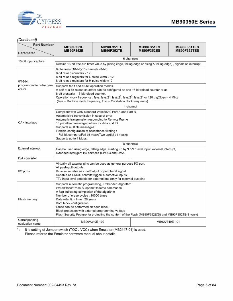
(Continued)
* : It is setting of Jumper switch (TOOL VCC) when Emulator (MB2147-01) is used.Please refer to the Emulator hardware manual about details.
Part Number
Parameter
MB90F351EMB90F352E
MB90F351TEMB90F352TE
MB90F351ESMB90F352ES
MB90F351TESMB90F352TES
16-bit Input capture6 channels
Retains 16-bit free-run timer value by (rising edge, falling edge or rising & falling edge) , signals an interrupt.
8/16-bit programmable pulse gen-erator
6 channels (16-bit)/10 channels (8-bit)8-bit reload counters 128-bit reload registers for L pulse width 128-bit reload registers for H pulse width12
Supports 8-bit and 16-bit operation modes.A pair of 8-bit reload counters can be configured as one 16-bit reload counter or as8-bit prescaler 8-bit reload counter.Operation clock frequency : fsys, fsys/21, fsys/22, fsys/23, fsys/24 or 128 s@fosc 4 MHz (fsys Machine clock frequency, fosc Oscillation clock frequency)
CAN interface
1 channel
Compliant with CAN standard Version2.0 Part A and Part B.Automatic re-transmission in case of errorAutomatic transmission responding to Remote Frame16 prioritized message buffers for data and IDSupports multiple messages.Flexible configuration of acceptance filtering : Full bit compare/Full bit mask/Two partial bit masksSupports up to 1 Mbps.
External interrupt
8 channels
Can be used rising edge, falling edge, starting up by “H”/“L” level input, external interrupt, extended intelligent I/O services (EI2OS) and DMA.
D/A converter
I/O ports
Virtually all external pins can be used as general purpose I/O port.All push-pull outputsBit-wise settable as input/output or peripheral signalSettable as CMOS schmitt trigger/ automotive inputsTTL input level settable for external bus (only for external bus pin)
Flash memory
Supports automatic programming, Embedded AlgorithmWrite/Erase/Erase-Suspend/Resume commandsA flag indicating completion of the algorithmNumber of erase cycles : 10000 timesData retention time : 20 yearsBoot block configurationErase can be performed on each block.Block protection with external programming voltageFlash Security Feature for protecting the content of the Flash (MB90F352E(S) and MB90F352TE(S) only)
Corresponding evaluation name
MB90V340E-102 MB90V340E-101
MB90350E Series
Document Number: 002-04493 Rev. *A Page 6 of 84
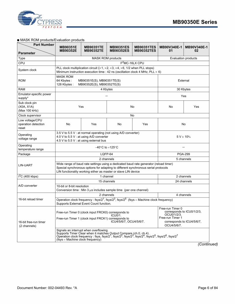
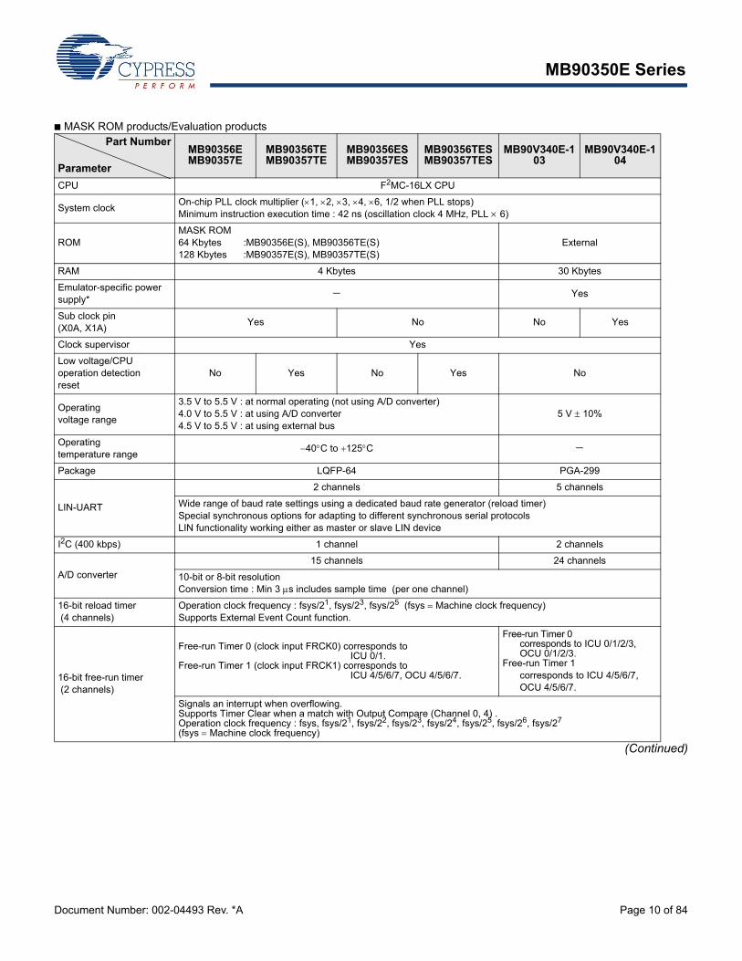
■ MASK ROM products/Evaluation products
(Continued)
Part Number
Parameter
MB90351EMB90352E
MB90351TEMB90352TE
MB90351ESMB90352ES
MB90351TESMB90352TES
MB90V340E-101
MB90V340E-102
Type MASK ROM products Evaluation products
CPU F2MC-16LX CPU
System clockPLL clock multiplication circuit (1, 2, 3, 4, 6, 1/2 when PLL stops) Minimum instruction execution time : 42 ns (oscillation clock 4 MHz, PLL 6)
ROMMASK ROM64 Kbytes : MB90351E(S), MB90351TE(S)128 Kbytes : MB90352E(S), MB90352TE(S)
External
RAM 4 Kbytes 30 Kbytes
Emulator-specific power supply*
Yes
Sub clock pin(X0A, X1A)(Max 100 kHz)
Yes No No Yes
Clock supervisor No
Low voltage/CPU operation detection reset
No Yes No Yes No
Operating voltage range
3.5 V to 5.5 V : at normal operating (not using A/D converter)4.0 V to 5.5 V : at using A/D converter4.5 V to 5.5 V : at using external bus
5 V 10
Operating temperature range
40C to 125C
Package LQFP-64 PGA-299
LIN-UART
2 channels 5 channels
Wide range of baud rate settings using a dedicated baud rate generator (reload timer)Special synchronous options for adapting to different synchronous serial protocolsLIN functionality working either as master or slave LIN device
I2C (400 kbps) 1 channel 2 channels
A/D converter
15 channels 24 channels
10-bit or 8-bit resolutionConversion time : Min 3 s includes sample time (per one channel)
16-bit reload timer
2 channels 4 channels
Operation clock frequency : fsys/21, fsys/23, fsys/25 (fsys Machine clock frequency) Supports External Event Count function.
16-bit free-run timer (2 channels)
Free-run Timer 0 (clock input FRCK0) corresponds to ICU0/1.
Free-run Timer 1 (clock input FRCK1) corresponds to ICU4/5/6/7, OCU4/5/6/7.
Free-run Timer 0 corresponds to ICU0/1/2/3, OCU0/1/2/3.
Free-run Timer 1 corresponds to ICU4/5/6/7, OCU4/5/6/7.
Signals an interrupt when overflowing.Supports Timer Clear when it matches Output Compare (ch.0, ch.4) .Operation clock frequency : fsys, fsys/21, fsys/22, fsys/23, fsys/24, fsys/25, fsys/26, fsys/27
(fsys Machine clock frequency)
MB90350E Series
Document Number: 002-04493 Rev. *A Page 7 of 84
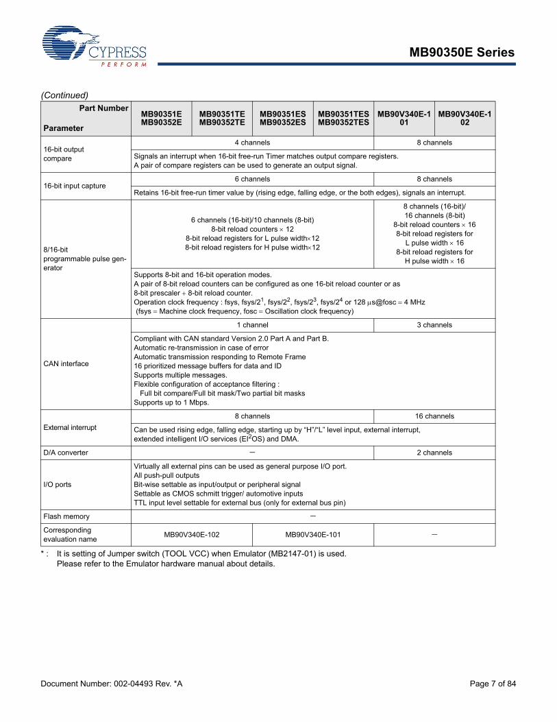
(Continued)
* : It is setting of Jumper switch (TOOL VCC) when Emulator (MB2147-01) is used.Please refer to the Emulator hardware manual about details.
Part Number
Parameter
MB90351EMB90352E
MB90351TEMB90352TE
MB90351ESMB90352ES
MB90351TESMB90352TES
MB90V340E-101
MB90V340E-102
16-bit output compare
4 channels 8 channels
Signals an interrupt when 16-bit free-run Timer matches output compare registers.A pair of compare registers can be used to generate an output signal.
16-bit input capture6 channels 8 channels
Retains 16-bit free-run timer value by (rising edge, falling edge, or the both edges), signals an interrupt.
8/16-bit programmable pulse gen-erator
6 channels (16-bit)/10 channels (8-bit)8-bit reload counters 12
8-bit reload registers for L pulse width128-bit reload registers for H pulse width12
8 channels (16-bit)/16 channels (8-bit)
8-bit reload counters 168-bit reload registers for
L pulse width 168-bit reload registers for
H pulse width 16
Supports 8-bit and 16-bit operation modes.A pair of 8-bit reload counters can be configured as one 16-bit reload counter or as8-bit prescaler 8-bit reload counter.Operation clock frequency : fsys, fsys/21, fsys/22, fsys/23, fsys/24 or 128 s@fosc 4 MHz (fsys Machine clock frequency, fosc Oscillation clock frequency)
CAN interface
1 channel 3 channels
Compliant with CAN standard Version 2.0 Part A and Part B.Automatic re-transmission in case of errorAutomatic transmission responding to Remote Frame16 prioritized message buffers for data and IDSupports multiple messages.Flexible configuration of acceptance filtering : Full bit compare/Full bit mask/Two partial bit masksSupports up to 1 Mbps.
External interrupt
8 channels 16 channels
Can be used rising edge, falling edge, starting up by “H”/“L” level input, external interrupt, extended intelligent I/O services (EI2OS) and DMA.
D/A converter 2 channels
I/O ports
Virtually all external pins can be used as general purpose I/O port.All push-pull outputsBit-wise settable as input/output or peripheral signalSettable as CMOS schmitt trigger/ automotive inputsTTL input level settable for external bus (only for external bus pin)
Flash memory Corresponding evaluation name
MB90V340E-102 MB90V340E-101
MB90350E Series
Document Number: 002-04493 Rev. *A Page 8 of 84
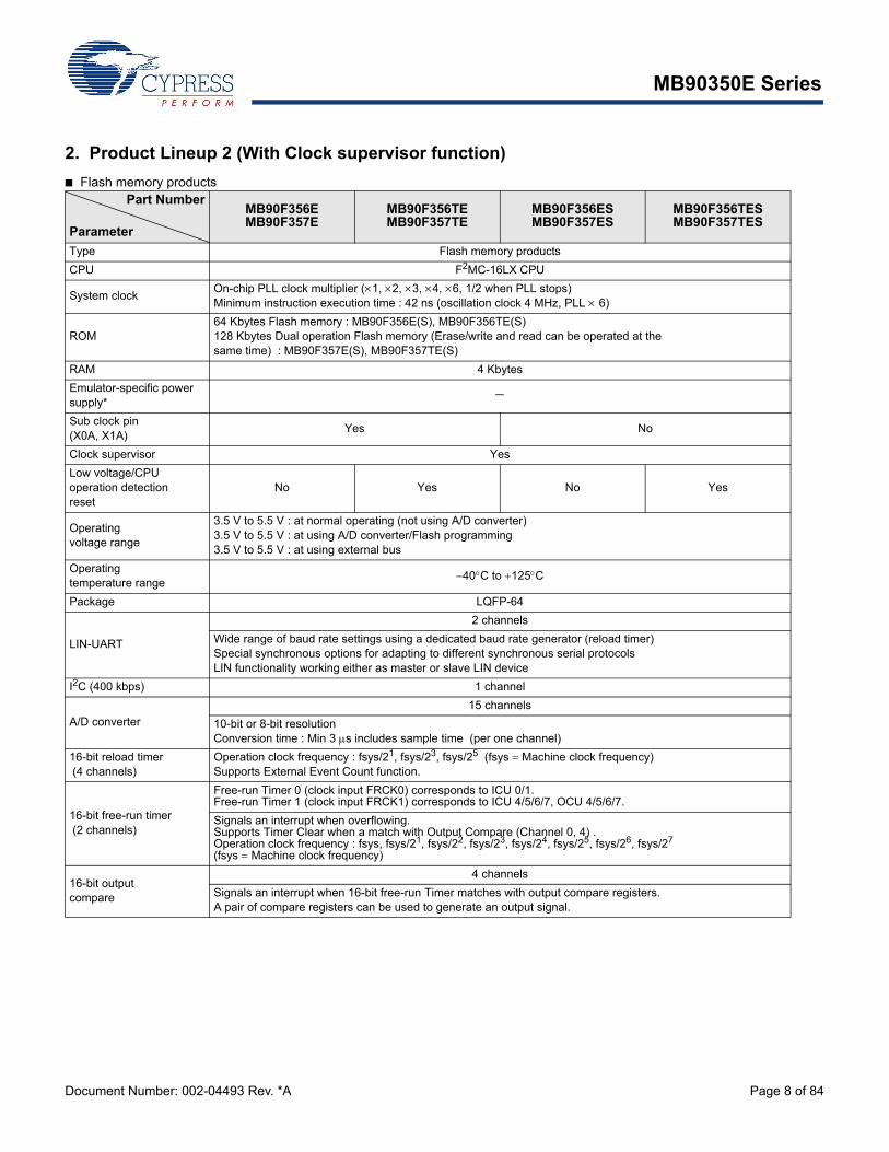
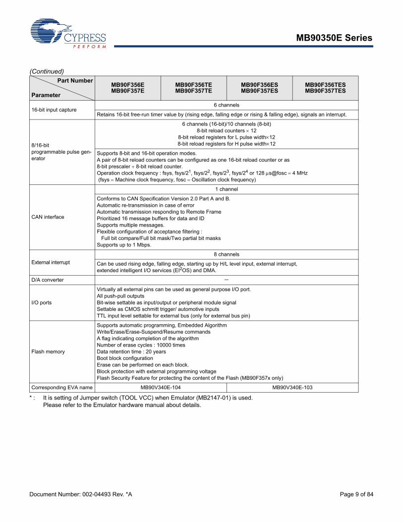
2. Product Lineup 2 (With Clock supervisor function)
■ Flash memory productsPart Number
Parameter
MB90F356EMB90F357E
MB90F356TEMB90F357TE
MB90F356ESMB90F357ES
MB90F356TESMB90F357TES
Type Flash memory products
CPU F2MC-16LX CPU
System clockOn-chip PLL clock multiplier (1, 2, 3, 4, 6, 1/2 when PLL stops) Minimum instruction execution time : 42 ns (oscillation clock 4 MHz, PLL 6)
ROM64 Kbytes Flash memory : MB90F356E(S), MB90F356TE(S)128 Kbytes Dual operation Flash memory (Erase/write and read can be operated at the same time) : MB90F357E(S), MB90F357TE(S)
RAM 4 Kbytes
Emulator-specific power supply*
Sub clock pin(X0A, X1A)
Yes No
Clock supervisor Yes
Low voltage/CPU operation detection reset
No Yes No Yes
Operating voltage range
3.5 V to 5.5 V : at normal operating (not using A/D converter)3.5 V to 5.5 V : at using A/D converter/Flash programming3.5 V to 5.5 V : at using external bus
Operating temperature range
40C to 125C
Package LQFP-64
LIN-UART
2 channels
Wide range of baud rate settings using a dedicated baud rate generator (reload timer)Special synchronous options for adapting to different synchronous serial protocolsLIN functionality working either as master or slave LIN device
I2C (400 kbps) 1 channel
A/D converter
15 channels
10-bit or 8-bit resolutionConversion time : Min 3 s includes sample time (per one channel)
16-bit reload timer (4 channels)
Operation clock frequency : fsys/21, fsys/23, fsys/25 (fsys Machine clock frequency) Supports External Event Count function.
16-bit free-run timer (2 channels)
Free-run Timer 0 (clock input FRCK0) corresponds to ICU 0/1.Free-run Timer 1 (clock input FRCK1) corresponds to ICU 4/5/6/7, OCU 4/5/6/7.
Signals an interrupt when overflowing.Supports Timer Clear when a match with Output Compare (Channel 0, 4) .Operation clock frequency : fsys, fsys/21, fsys/22, fsys/23, fsys/24, fsys/25, fsys/26, fsys/27
(fsys Machine clock frequency)
16-bit output compare
4 channels
Signals an interrupt when 16-bit free-run Timer matches with output compare registers.A pair of compare registers can be used to generate an output signal.
MB90350E Series
Document Number: 002-04493 Rev. *A Page 9 of 84
(Continued)
* : It is setting of Jumper switch (TOOL VCC) when Emulator (MB2147-01) is used.Please refer to the Emulator hardware manual about details.
Part Number
Parameter
MB90F356EMB90F357E
MB90F356TEMB90F357TE
MB90F356ESMB90F357ES
MB90F356TESMB90F357TES
16-bit input capture6 channels
Retains 16-bit free-run timer value by (rising edge, falling edge or rising & falling edge), signals an interrupt.
8/16-bit programmable pulse gen-erator
6 channels (16-bit)/10 channels (8-bit)8-bit reload counters 12
8-bit reload registers for L pulse width128-bit reload registers for H pulse width12
Supports 8-bit and 16-bit operation modes.A pair of 8-bit reload counters can be configured as one 16-bit reload counter or as8-bit prescaler 8-bit reload counter.Operation clock frequency : fsys, fsys/21, fsys/22, fsys/23, fsys/24 or 128 s@fosc 4 MHz (fsys Machine clock frequency, fosc Oscillation clock frequency)
CAN interface
1 channel
Conforms to CAN Specification Version 2.0 Part A and B.Automatic re-transmission in case of errorAutomatic transmission responding to Remote FramePrioritized 16 message buffers for data and IDSupports multiple messages.Flexible configuration of acceptance filtering : Full bit compare/Full bit mask/Two partial bit masksSupports up to 1 Mbps.
External interrupt
8 channels
Can be used rising edge, falling edge, starting up by H/L level input, external interrupt, extended intelligent I/O services (EI2OS) and DMA.
D/A converter
I/O ports
Virtually all external pins can be used as general purpose I/O port.All push-pull outputsBit-wise settable as input/output or peripheral module signalSettable as CMOS schmitt trigger/ automotive inputsTTL input level settable for external bus (only for external bus pin)
Flash memory
Supports automatic programming, Embedded AlgorithmWrite/Erase/Erase-Suspend/Resume commandsA flag indicating completion of the algorithmNumber of erase cycles : 10000 timesData retention time : 20 yearsBoot block configurationErase can be performed on each block.Block protection with external programming voltageFlash Security Feature for protecting the content of the Flash (MB90F357x only)
Corresponding EVA name MB90V340E-104 MB90V340E-103
MB90350E Series
Document Number: 002-04493 Rev. *A Page 10 of 84
■ MASK ROM products/Evaluation products
(Continued)
Part Number
Parameter
MB90356EMB90357E
MB90356TEMB90357TE
MB90356ESMB90357ES
MB90356TESMB90357TES
MB90V340E-103
MB90V340E-104
CPU F2MC-16LX CPU
System clockOn-chip PLL clock multiplier (1, 2, 3, 4, 6, 1/2 when PLL stops) Minimum instruction execution time : 42 ns (oscillation clock 4 MHz, PLL 6)
ROMMASK ROM64 Kbytes :MB90356E(S), MB90356TE(S)128 Kbytes :MB90357E(S), MB90357TE(S)
External
RAM 4 Kbytes 30 Kbytes
Emulator-specific power supply*
Yes
Sub clock pin(X0A, X1A)
Yes No No Yes
Clock supervisor Yes
Low voltage/CPU operation detection reset
No Yes No Yes No
Operating voltage range
3.5 V to 5.5 V : at normal operating (not using A/D converter)4.0 V to 5.5 V : at using A/D converter4.5 V to 5.5 V : at using external bus
5 V 10%
Operating temperature range
40C to 125C
Package LQFP-64 PGA-299
LIN-UART
2 channels 5 channels
Wide range of baud rate settings using a dedicated baud rate generator (reload timer)Special synchronous options for adapting to different synchronous serial protocolsLIN functionality working either as master or slave LIN device
I2C (400 kbps) 1 channel 2 channels
A/D converter
15 channels 24 channels
10-bit or 8-bit resolutionConversion time : Min 3 s includes sample time (per one channel)
16-bit reload timer (4 channels)
Operation clock frequency : fsys/21, fsys/23, fsys/25 (fsys Machine clock frequency) Supports External Event Count function.
16-bit free-run timer (2 channels)
Free-run Timer 0 (clock input FRCK0) corresponds to ICU 0/1.
Free-run Timer 1 (clock input FRCK1) corresponds to ICU 4/5/6/7, OCU 4/5/6/7.
Free-run Timer 0 corresponds to ICU 0/1/2/3, OCU 0/1/2/3.
Free-run Timer 1 corresponds to ICU 4/5/6/7, OCU 4/5/6/7.
Signals an interrupt when overflowing.Supports Timer Clear when a match with Output Compare (Channel 0, 4) .Operation clock frequency : fsys, fsys/21, fsys/22, fsys/23, fsys/24, fsys/25, fsys/26, fsys/27
(fsys Machine clock frequency)

MB90350E Series
Document Number: 002-04493 Rev. *A Page 11 of 84
(Continued)
* : It is setting of Jumper switch (TOOL VCC) when Emulator (MB2147-01) is used.Please refer to the Emulator hardware manual about details.
Part Number
Parameter
MB90356EMB90357E
MB90356TEMB90357TE
MB90356ESMB90357ES
MB90356TESMB90357TES
MB90V340E-103
MB90V340E-104
16-bit output compare
4 channels 8 channels
Signals an interrupt when 16-bit free-run Timer matches with output compare registers.A pair of compare registers can be used to generate an output signal.
16-bit input capture
6 channels 8 channels
Retains 16-bit free-run timer value by (rising edge, falling edge or rising & falling edge), signals an interrupt.
8/16-bit programmable pulse gen-erator
6 channels (16-bit)/10 channels (8-bit)8-bit reload counters12
8-bit reload registers for L pulse width 128-bit reload registers for H pulse width 12
8 channels (16-bit)/16 channels (8-bit)
8-bit reload counters168-bit reload registers for
L pulse width168-bit reload registers for
H pulse width16
Supports 8-bit and 16-bit operation modes.A pair of 8-bit reload counters can be configured as one 16-bit reload counter or as 8-bit prescaler 8-bit reload counter.Operation clock frequency : fsys, fsys/21, fsys/22, fsys/23, fsys/24 or 128 s@fosc 4 MHz (fsys Machine clock frequency, fosc Oscillation clock frequency)
CAN interface
1 channel 3 channels
Conforms to CAN Specification Version 2.0 Part A and B.Automatic re-transmission in case of errorAutomatic transmission responding to Remote FramePrioritized 16 message buffers for data and IDSupports multiple messages.Flexible configuration of acceptance filtering : Full bit compare/Full bit mask/Two partial bit masksSupports up to 1 Mbps.
External interrupt
8 channels 16 channels
Can be used rising edge, falling edge, starting up by H/L level input, external interrupt, extended intelligent I/O services (EI2OS) and DMA.
D/A converter 2 channels
I/O ports
Virtually all external pins can be used as general purpose I/O port.All push-pull outputsBit-wise settable as input/output or peripheral module signalSettable as CMOS schmitt trigger/ automotive inputsTTL input level settable for external bus (only for external bus pin)
Flash memory Corresponding EVA name MB90V340E-104 MB90V340E-103
MB90350E Series
Document Number: 002-04493 Rev. *A Page 12 of 84
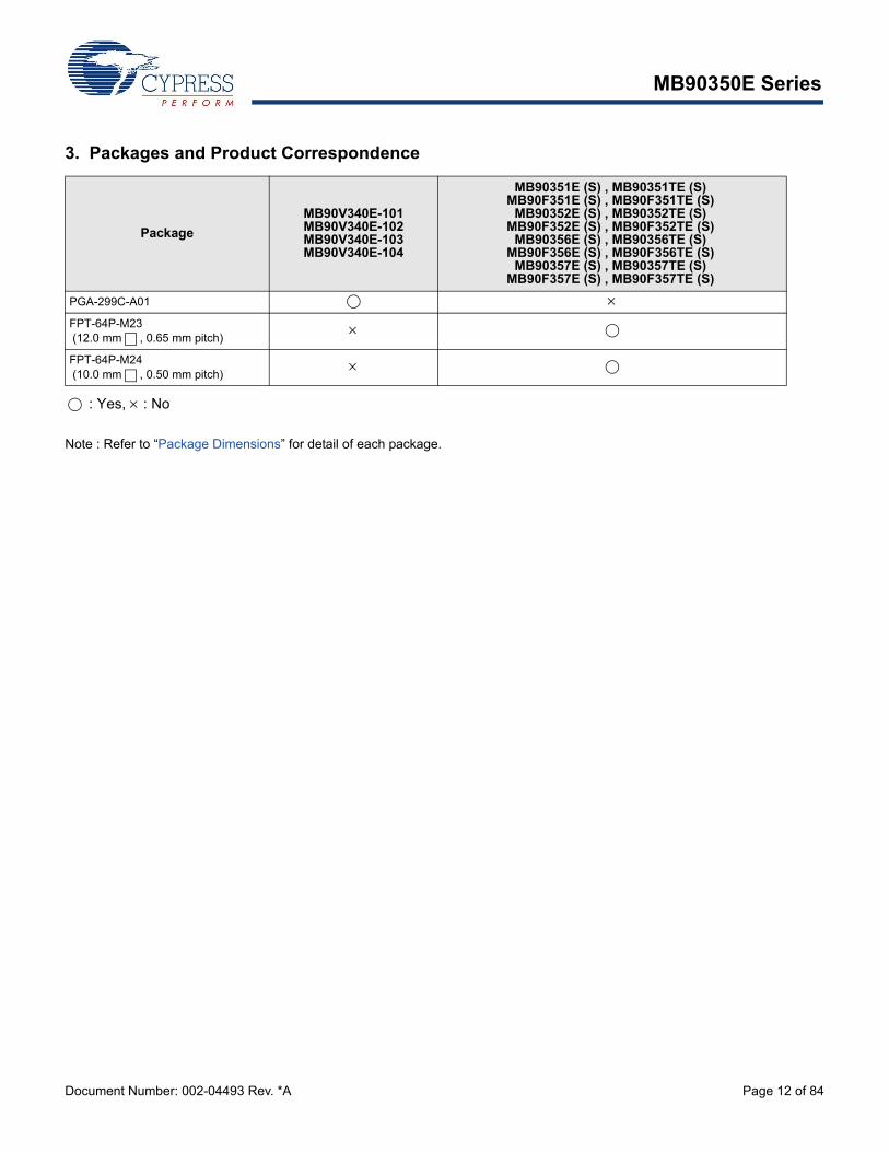
3. Packages and Product Correspondence
: Yes, : No
Note : Refer to “Package Dimensions” for detail of each package.
Package
MB90V340E-101MB90V340E-102MB90V340E-103MB90V340E-104
MB90351E (S) , MB90351TE (S) MB90F351E (S) , MB90F351TE (S)
MB90352E (S) , MB90352TE (S) MB90F352E (S) , MB90F352TE (S)
MB90356E (S) , MB90356TE (S) MB90F356E (S) , MB90F356TE (S)
MB90357E (S) , MB90357TE (S) MB90F357E (S) , MB90F357TE (S)
PGA-299C-A01 FPT-64P-M23 (12.0 mm , 0.65 mm pitch)
FPT-64P-M24 (10.0 mm , 0.50 mm pitch)
MB90350E Series
Document Number: 002-04493 Rev. *A Page 13 of 84
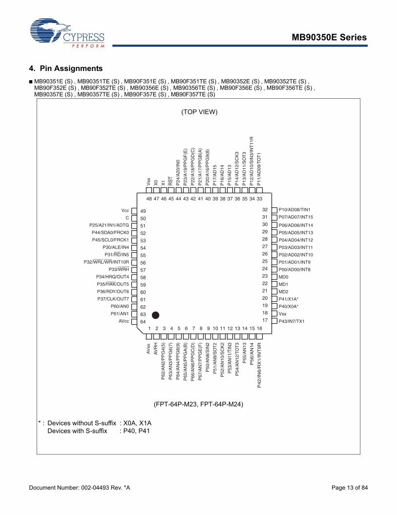
4. Pin Assignments
■ MB90351E (S) , MB90351TE (S) , MB90F351E (S) , MB90F351TE (S) , MB90352E (S) , MB90352TE (S) , MB90F352E (S) , MB90F352TE (S) , MB90356E (S) , MB90356TE (S) , MB90F356E (S) , MB90F356TE (S) , MB90357E (S) , MB90357TE (S) , MB90F357E (S) , MB90F357TE (S)
(TOP VIEW)
(FPT-64P-M23, FPT-64P-M24)
* : Devices without S-suffix : X0A, X1ADevices with S-suffix : P40, P41
48 47 46 45 44 43 42 41 40 39 38 37 36 35 34 33
64
63
62
61
60
59
58
57
56
55
54
53
52
51
50
49
17
18
19
20
21
22
23
24
25
26
27
28
29
30
31
32
AVcc
P61/AN1
P60/AN0
P37/CLK/OUT7
P36/RDY/OUT6
P35/HAK/OUT5
P34/HRQ/OUT4
P32/WRL/WR/INT10R
P31/RD/IN5
P30/ALE/IN4
P45/SCL0/FRCK1
P44/SDA0/FRCK0
P25/A21/IN1/ADTG
C
Vcc
P33/WRH
10 11 12 13 14 15 161 2 3 4 5 6 7 98
P10/AD08/TIN1
P07/AD07/INT15
P06/AD06/INT14
P05/AD05/INT13
P04/AD04/INT12
P03/AD03/INT11
P02/AD02/INT10
P01/AD01/INT9
P00/AD00/INT8
MD0
MD1
MD2
P41/X1A*
P40/X0A*
Vss
P43/IN7/TX1
Vss
X0
X1
RS
T
P24
/A20
/IN0
P23
/A19
/PP
GF
(E)
P22
/A18
/PP
GD
(C)
P21
/A17
/PP
GB
(A)
P20
/A16
/PP
G9(
8)
P17
/AD
15
P16
/AD
14
P15
/AD
13
P14
/AD
12/S
CK
3
P13
/AD
11/S
OT
3
P12
/AD
10/S
IN3/
INT
11R
P11
/AD
09/T
OT
1
AV
ss
AV
RH
P64
/AN
4/P
PG
8(9)
P65
/AN
5/P
PG
A(B
)
P66
/AN
6/P
PG
C(D
)
P67
/AN
7/P
PG
E(F
)
P50
/AN
8/S
IN2
P51
/AN
9/S
OT
2
P52
/AN
10/S
CK
2
P53
/AN
11/T
IN3
P56/A
N14
P55
/AN
13
P54
/AN
12/T
OT
3
P62
/AN
2/P
PG
4(5)
P63
/AN
3/P
PG
6(7)
P42/IN
6/R
X1/IN
T9R
MB90350E Series
Document Number: 002-04493 Rev. *A Page 14 of 84
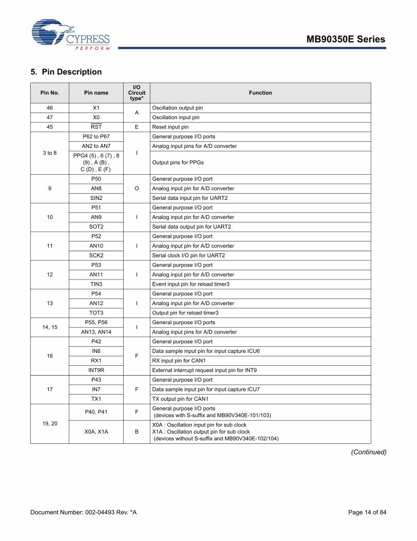
5. Pin Description
(Continued)
Pin No. Pin nameI/O
Circuit type*
Function
46 X1A
Oscillation output pin
47 X0 Oscillation input pin
45 RST E Reset input pin
3 to 8
P62 to P67
I
General purpose I/O ports
AN2 to AN7 Analog input pins for A/D converter
PPG4 (5) , 6 (7) , 8 (9) , A (B) ,
C (D) , E (F) Output pins for PPGs
9
P50
O
General purpose I/O port
AN8 Analog input pin for A/D converter
SIN2 Serial data input pin for UART2
10
P51
I
General purpose I/O port
AN9 Analog input pin for A/D converter
SOT2 Serial data output pin for UART2
11
P52
I
General purpose I/O port
AN10 Analog input pin for A/D converter
SCK2 Serial clock I/O pin for UART2
12
P53
I
General purpose I/O port
AN11 Analog input pin for A/D converter
TIN3 Event input pin for reload timer3
13
P54
I
General purpose I/O port
AN12 Analog input pin for A/D converter
TOT3 Output pin for reload timer3
14, 15P55, P56
IGeneral purpose I/O ports
AN13, AN14 Analog input pins for A/D converter
16
P42
F
General purpose I/O port
IN6 Data sample input pin for input capture ICU6
RX1 RX input pin for CAN1
INT9R External interrupt request input pin for INT9
17
P43
F
General purpose I/O port
IN7 Data sample input pin for input capture ICU7
TX1 TX output pin for CAN1
19, 20
P40, P41 FGeneral purpose I/O ports (devices with S-suffix and MB90V340E-101/103)
X0A, X1A BX0A : Oscillation input pin for sub clockX1A : Oscillation output pin for sub clock (devices without S-suffix and MB90V340E-102/104)
MB90350E Series
Document Number: 002-04493 Rev. *A Page 15 of 84
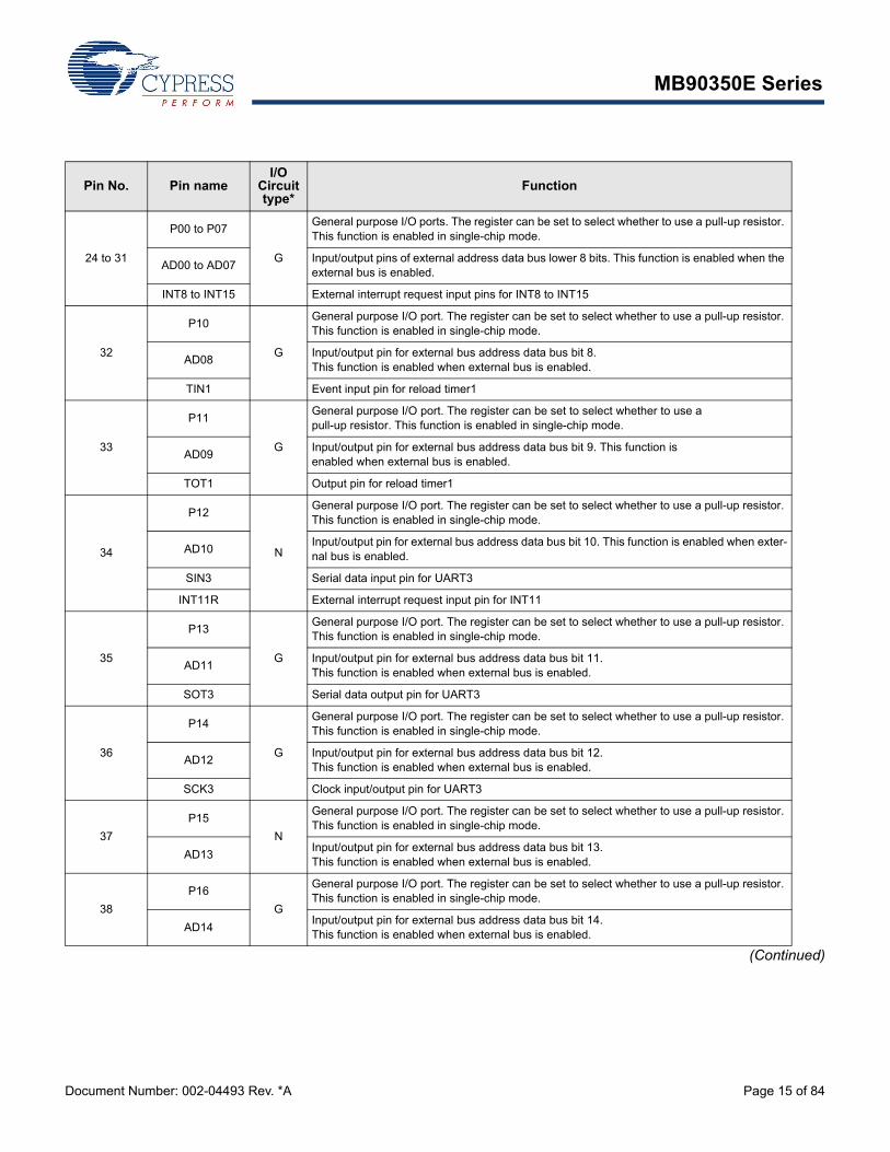
(Continued)
Pin No. Pin nameI/O
Circuit type*
Function
24 to 31
P00 to P07
G
General purpose I/O ports. The register can be set to select whether to use a pull-up resistor. This function is enabled in single-chip mode.
AD00 to AD07Input/output pins of external address data bus lower 8 bits. This function is enabled when the external bus is enabled.
INT8 to INT15 External interrupt request input pins for INT8 to INT15
32
P10
G
General purpose I/O port. The register can be set to select whether to use a pull-up resistor. This function is enabled in single-chip mode.
AD08Input/output pin for external bus address data bus bit 8. This function is enabled when external bus is enabled.
TIN1 Event input pin for reload timer1
33
P11
G
General purpose I/O port. The register can be set to select whether to use a pull-up resistor. This function is enabled in single-chip mode.
AD09Input/output pin for external bus address data bus bit 9. This function is enabled when external bus is enabled.
TOT1 Output pin for reload timer1
34
P12
N
General purpose I/O port. The register can be set to select whether to use a pull-up resistor. This function is enabled in single-chip mode.
AD10Input/output pin for external bus address data bus bit 10. This function is enabled when exter-nal bus is enabled.
SIN3 Serial data input pin for UART3
INT11R External interrupt request input pin for INT11
35
P13
G
General purpose I/O port. The register can be set to select whether to use a pull-up resistor. This function is enabled in single-chip mode.
AD11Input/output pin for external bus address data bus bit 11. This function is enabled when external bus is enabled.
SOT3 Serial data output pin for UART3
36
P14
G
General purpose I/O port. The register can be set to select whether to use a pull-up resistor. This function is enabled in single-chip mode.
AD12Input/output pin for external bus address data bus bit 12. This function is enabled when external bus is enabled.
SCK3 Clock input/output pin for UART3
37
P15
N
General purpose I/O port. The register can be set to select whether to use a pull-up resistor. This function is enabled in single-chip mode.
AD13Input/output pin for external bus address data bus bit 13. This function is enabled when external bus is enabled.
38
P16
G
General purpose I/O port. The register can be set to select whether to use a pull-up resistor. This function is enabled in single-chip mode.
AD14Input/output pin for external bus address data bus bit 14. This function is enabled when external bus is enabled.
MB90350E Series
Document Number: 002-04493 Rev. *A Page 16 of 84
(Continued)
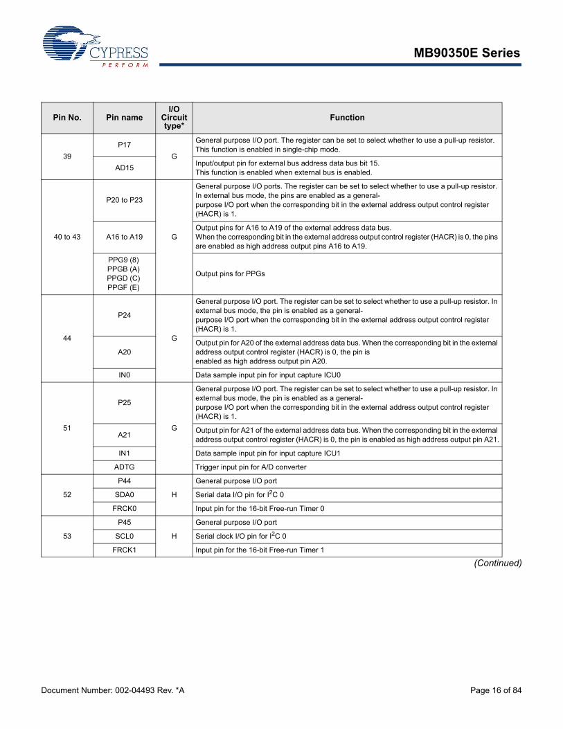
Pin No. Pin nameI/O
Circuit type*
Function
39
P17
G
General purpose I/O port. The register can be set to select whether to use a pull-up resistor. This function is enabled in single-chip mode.
AD15Input/output pin for external bus address data bus bit 15. This function is enabled when external bus is enabled.
40 to 43
P20 to P23
G
General purpose I/O ports. The register can be set to select whether to use a pull-up resistor. In external bus mode, the pins are enabled as a general-purpose I/O port when the corresponding bit in the external address output control register (HACR) is 1.
A16 to A19Output pins for A16 to A19 of the external address data bus. When the corresponding bit in the external address output control register (HACR) is 0, the pins are enabled as high address output pins A16 to A19.
PPG9 (8) PPGB (A) PPGD (C) PPGF (E)
Output pins for PPGs
44
P24
G
General purpose I/O port. The register can be set to select whether to use a pull-up resistor. In external bus mode, the pin is enabled as a general-purpose I/O port when the corresponding bit in the external address output control register (HACR) is 1.
A20Output pin for A20 of the external address data bus. When the corresponding bit in the external address output control register (HACR) is 0, the pin is enabled as high address output pin A20.
IN0 Data sample input pin for input capture ICU0
51
P25
G
General purpose I/O port. The register can be set to select whether to use a pull-up resistor. In external bus mode, the pin is enabled as a general-purpose I/O port when the corresponding bit in the external address output control register (HACR) is 1.
A21Output pin for A21 of the external address data bus. When the corresponding bit in the external address output control register (HACR) is 0, the pin is enabled as high address output pin A21.
IN1 Data sample input pin for input capture ICU1
ADTG Trigger input pin for A/D converter
52
P44
H
General purpose I/O port
SDA0 Serial data I/O pin for I2C 0
FRCK0 Input pin for the 16-bit Free-run Timer 0
53
P45
H
General purpose I/O port
SCL0 Serial clock I/O pin for I2C 0
FRCK1 Input pin for the 16-bit Free-run Timer 1
MB90350E Series
Document Number: 002-04493 Rev. *A Page 17 of 84
(Continued)
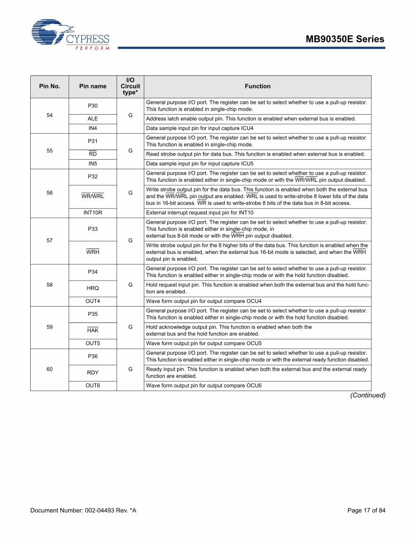
Pin No. Pin nameI/O
Circuit type*
Function
54
P30
G
General purpose I/O port. The register can be set to select whether to use a pull-up resistor. This function is enabled in single-chip mode.
ALE Address latch enable output pin. This function is enabled when external bus is enabled.
IN4 Data sample input pin for input capture ICU4
55
P31
G
General purpose I/O port. The register can be set to select whether to use a pull-up resistor. This function is enabled in single-chip mode.
RD Read strobe output pin for data bus. This function is enabled when external bus is enabled.
IN5 Data sample input pin for input capture ICU5
56
P32
G
General purpose I/O port. The register can be set to select whether to use a pull-up resistor. This function is enabled either in single-chip mode or with the WR/WRL pin output disabled.
WR/WRLWrite strobe output pin for the data bus. This function is enabled when both the external bus and the WR/WRL pin output are enabled. WRL is used to write-strobe 8 lower bits of the data bus in 16-bit access. WR is used to write-strobe 8 bits of the data bus in 8-bit access.
INT10R External interrupt request input pin for INT10
57
P33
G
General purpose I/O port. The register can be set to select whether to use a pull-up resistor. This function is enabled either in single-chip mode, in external bus 8-bit mode or with the WRH pin output disabled.
WRHWrite strobe output pin for the 8 higher bits of the data bus. This function is enabled when the external bus is enabled, when the external bus 16-bit mode is selected, and when the WRH output pin is enabled.
58
P34
G
General purpose I/O port. The register can be set to select whether to use a pull-up resistor. This function is enabled either in single-chip mode or with the hold function disabled.
HRQHold request input pin. This function is enabled when both the external bus and the hold func-tion are enabled.
OUT4 Wave form output pin for output compare OCU4
59
P35
G
General purpose I/O port. The register can be set to select whether to use a pull-up resistor. This function is enabled either in single-chip mode or with the hold function disabled.
HAKHold acknowledge output pin. This function is enabled when both the external bus and the hold function are enabled.
OUT5 Wave form output pin for output compare OCU5
60
P36
G
General purpose I/O port. The register can be set to select whether to use a pull-up resistor. This function is enabled either in single-chip mode or with the external ready function disabled.
RDYReady input pin. This function is enabled when both the external bus and the external ready function are enabled.
OUT6 Wave form output pin for output compare OCU6
MB90350E Series
Document Number: 002-04493 Rev. *A Page 18 of 84
(Continued)
* : For the I/O circuit type, refer to “I/O Circuit Type”.
Pin No. Pin nameI/O
Circuit type*
Function
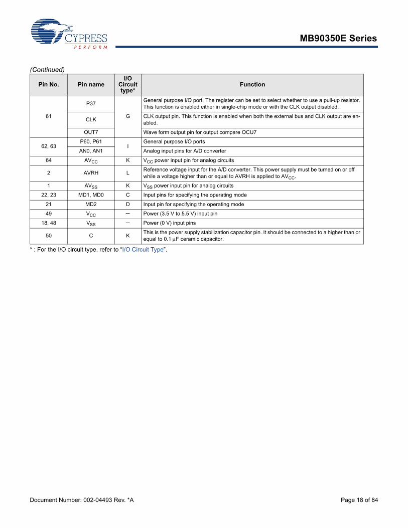
61
P37
G
General purpose I/O port. The register can be set to select whether to use a pull-up resistor. This function is enabled either in single-chip mode or with the CLK output disabled.
CLKCLK output pin. This function is enabled when both the external bus and CLK output are en-abled.
OUT7 Wave form output pin for output compare OCU7
62, 63P60, P61
IGeneral purpose I/O ports
AN0, AN1 Analog input pins for A/D converter
64 AVCC K VCC power input pin for analog circuits
2 AVRH LReference voltage input for the A/D converter. This power supply must be turned on or off while a voltage higher than or equal to AVRH is applied to AVCC.
1 AVSS K VSS power input pin for analog circuits
22, 23 MD1, MD0 C Input pins for specifying the operating mode
21 MD2 D Input pin for specifying the operating mode
49 VCC Power (3.5 V to 5.5 V) input pin
18, 48 VSS Power (0 V) input pins
50 C KThis is the power supply stabilization capacitor pin. It should be connected to a higher than or equal to 0.1 F ceramic capacitor.
MB90350E Series
Document Number: 002-04493 Rev. *A Page 19 of 84
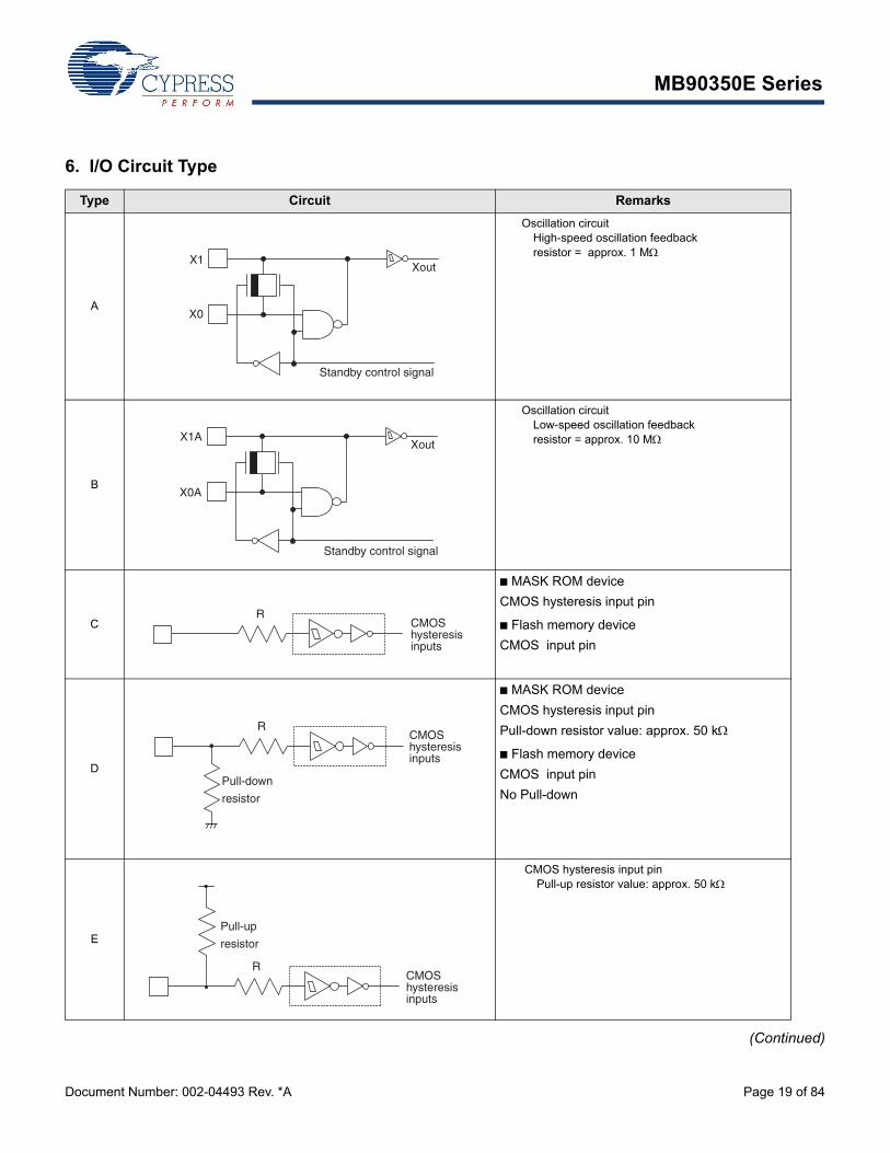
6. I/O Circuit Type
(Continued)
Type Circuit Remarks
A
Oscillation circuitHigh-speed oscillation feedback resistor = approx. 1 M
B
Oscillation circuitLow-speed oscillation feedback resistor = approx. 10 M
C
■ MASK ROM device
CMOS hysteresis input pin
■ Flash memory device
CMOS input pin
D
■ MASK ROM device
CMOS hysteresis input pin
Pull-down resistor value: approx. 50 k
■ Flash memory device
CMOS input pin
No Pull-down
E
CMOS hysteresis input pinPull-up resistor value: approx. 50 k
Standby control signal
X1
X0
Xout
Standby control signal
X1A
X0A
Xout
CMOShysteresisinputs
R
Pull-down
resistor
CMOShysteresisinputs
R
Pull-up
resistor
CMOShysteresisinputs
R
MB90350E Series
Document Number: 002-04493 Rev. *A Page 20 of 84
(Continued)
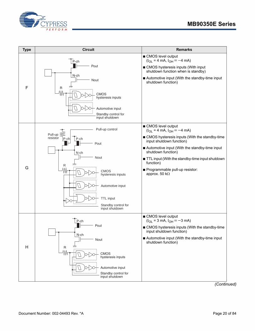
Type Circuit Remarks
F
■ CMOS level output(IOL = 4 mA, IOH 4 mA)
■ CMOS hysteresis inputs (With input shutdown function when is standby)
■ Automotive input (With the standby-time input shutdown function)
G
■ CMOS level output(IOL = 4 mA, IOH 4 mA)
■ CMOS hysteresis inputs (With the standby-time input shutdown function)
■ Automotive input (With the standby-time input shutdown function)
■ TTL input (With the standby-time input shutdown function)
■ Programmable pull-up resistor: approx. 50 k
H
■ CMOS level output(IOL = 3 mA, IOH 3 mA)
■ CMOS hysteresis inputs (With the standby-time input shutdown function)
■ Automotive input (With the standby-time input shutdown function)
CMOShysteresis inputs
Automotive input
Standby control forinput shutdown
Pout
Nout
R
P-ch
N-ch
Pull-up control
CMOShysteresis inputs
Automotive input
TTL input
Standby control forinput shutdown
Pull-up resistor
Pout
Nout
R
P-chP-ch
N-ch
CMOShysteresis inputs
Automotive input
Standby control forinput shutdown
Pout
Nout
R
P-ch
N-ch
MB90350E Series
Document Number: 002-04493 Rev. *A Page 21 of 84
(Continued)
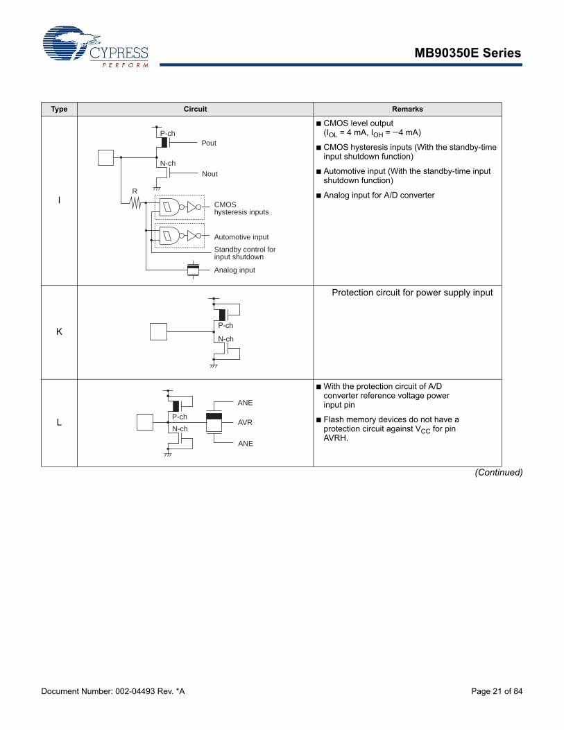
Type Circuit Remarks
I
■ CMOS level output (IOL = 4 mA, IOH = 4 mA)
■ CMOS hysteresis inputs (With the standby-time input shutdown function)
■ Automotive input (With the standby-time input shutdown function)
■ Analog input for A/D converter
K
Protection circuit for power supply input
L
■ With the protection circuit of A/D converter reference voltage power input pin
■ Flash memory devices do not have a protection circuit against VCC for pin AVRH.
CMOShysteresis inputs
Automotive input
Standby control forinput shutdown
Analog input
Pout
Nout
R
P-ch
N-ch
P-ch
N-ch
ANE
AVR
ANE
P-ch
N-ch
MB90350E Series
Document Number: 002-04493 Rev. *A Page 22 of 84
(Continued)
7. Handling Devices
1. Preventing latch-up
CMOS IC may suffer latch-up under the following conditions :
■A voltage higher than VCC or lower than VSS is applied to an input or output pin.
■A voltage higher than the rated voltage is applied between VCC and VSS pins.
■The AVCC power supply is applied before the VCC voltage.
Latch-up may increase the power supply current drastically, causing thermal damage to the device.
For the same reason, also be careful not to let the analog power-supply voltage (AVCC, AVRH) exceed the digital power-supplyvoltage (VCC) .
2. Treatment of unused pins
Leaving unused input pins open may result in misbehavior or latch up and possible permanent damage of the device. Thereforethey must be pulled up or pulled down through resistors. In this case those resistors should be more than 2 k.
Unused I/O pins should be set to the output state and can be left open, or the input state with the above described connection.
Type Circuit Remarks
N
■ CMOS level output(IOL = 4 mA, IOH 4 mA)
■ CMOS inputs (With the standby-time input shutdown function)
■ Automotive input (With the standby-time input shutdown function)
■ TTL input (With the standby-time input shutdown function)
■ Programmable pull-up resistor:approx. 50 k
O
■ CMOS level output(IOL = 4 mA, IOH 4 mA)
■ CMOS inputs (With the standby-time input shutdown function)
■ Automotive input (With the standby-time input shutdown function)
■ Analog input for A/D converter
Pull-up control
CMOS inputs
Automotive input
TTL input
Standby control forinput shutdown
Pull-up resistor
Pout
Nout
R
P-ch
N-ch
P-ch
CMOS inputs
Automotive input
Standby control forinput shutdown
Analog input
P-ch
N-ch
Pout
Nout
R
MB90350E Series
Document Number: 002-04493 Rev. *A Page 23 of 84
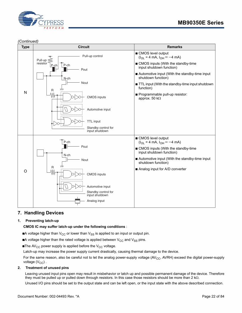
3. Using external clock
To use external clock, drive the X0 pin and leave X1 pin open.
4. Precautions for when not using a sub clock signal
X0A and X1A are oscillation pins for sub clock. If you do not connect pins X0A and X1A to an oscillator, use pull-down handling onthe X0A pin, and leave the X1A pin open.
5. Notes on during operation of PLL clock mode
On this microcontroller, if in case the crystal oscillator breaks off or an external reference clock input stops while the PLL clock modeis selected, a self-oscillator circuit contained in the PLL may continue its operation at its self-running frequency. However, Cypresswill not guarantee results of operations if such failure occurs.
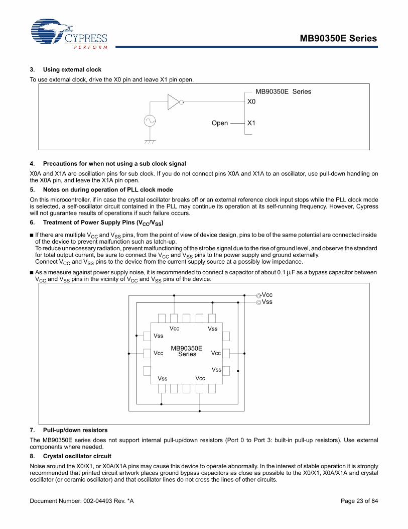
6. Treatment of Power Supply Pins (VCC/VSS)
■ If there are multiple VCC and VSS pins, from the point of view of device design, pins to be of the same potential are connected inside of the device to prevent malfunction such as latch-up.To reduce unnecessary radiation, prevent malfunctioning of the strobe signal due to the rise of ground level, and observe the standard for total output current, be sure to connect the VCC and VSS pins to the power supply and ground externally.Connect VCC and VSS pins to the device from the current supply source at a possibly low impedance.
■ As a measure against power supply noise, it is recommended to connect a capacitor of about 0.1 F as a bypass capacitor between VCC and VSS pins in the vicinity of VCC and VSS pins of the device.
7. Pull-up/down resistors
The MB90350E series does not support internal pull-up/down resistors (Port 0 to Port 3: built-in pull-up resistors). Use externalcomponents where needed.
8. Crystal oscillator circuit
Noise around the X0/X1, or X0A/X1A pins may cause this device to operate abnormally. In the interest of stable operation it is stronglyrecommended that printed circuit artwork places ground bypass capacitors as close as possible to the X0/X1, X0A/X1A and crystaloscillator (or ceramic oscillator) and that oscillator lines do not cross the lines of other circuits.
X0
X1
MB90350E Series
Open
VccVss
Vss
Vcc
Vss
VccMB90350E
Series
Vcc Vss
VccVss
MB90350E Series
Document Number: 002-04493 Rev. *A Page 24 of 84
Please ask each crystal maker to evaluate the oscillational characteristics of the crystal and this device.
9. Turning-on sequence of power supply to A/D converter and analog inputs
Make sure to turn on the A/D converter power supply (AVCC, AVRH) and analog inputs (AN0 to AN14) after turning-on the digital powersupply (VCC) .Turn-off the digital power after turning off the A/D converter powersupply and analog inputs. In this case, make sure that the power supply voltage does not exceed the rated voltage of the A/D converter(turning on/of the analog and digital power supplies simultaneously is acceptable).
10. Connection of unused pins of A/D converter if A/D converter is not used
Connect unused pins of A/D converter to AVCC VCC, AVSS AVRH VSS.
11. Notes on energization
To prevent the internal regulator circuit from malfunctioning, set the voltage rise time during energization at 50 s or more (0.2 V to 2.7 V) .
12. Stabilization of power supply voltage
A sudden change in the supply voltage may cause the device to malfunction even within the VCC supply voltage operating range.Therefore, the VCC supply voltage should be stabilized. For reference, the supply voltage should be controlled so that VCC ripplevariations (peak- to-peak values) at commercial frequencies (50 MHz/60 MHz) fall below 10 of the standard VCC supply voltage and the coefficient of fluctuation does not exceed 0.1 V/ms at instanta-neous power switching.
MB90350E Series
Document Number: 002-04493 Rev. *A Page 25 of 84
13. Serial Communication
There is a possibility to receive wrong data due to the noise or other causes on the serial communication. Therefore, design a printedcircuit board so as to avoid noise.
Retransmit the data if an error occurs because of applying the checksum to the last data in consideration of receiving wrong data dueto the noise.
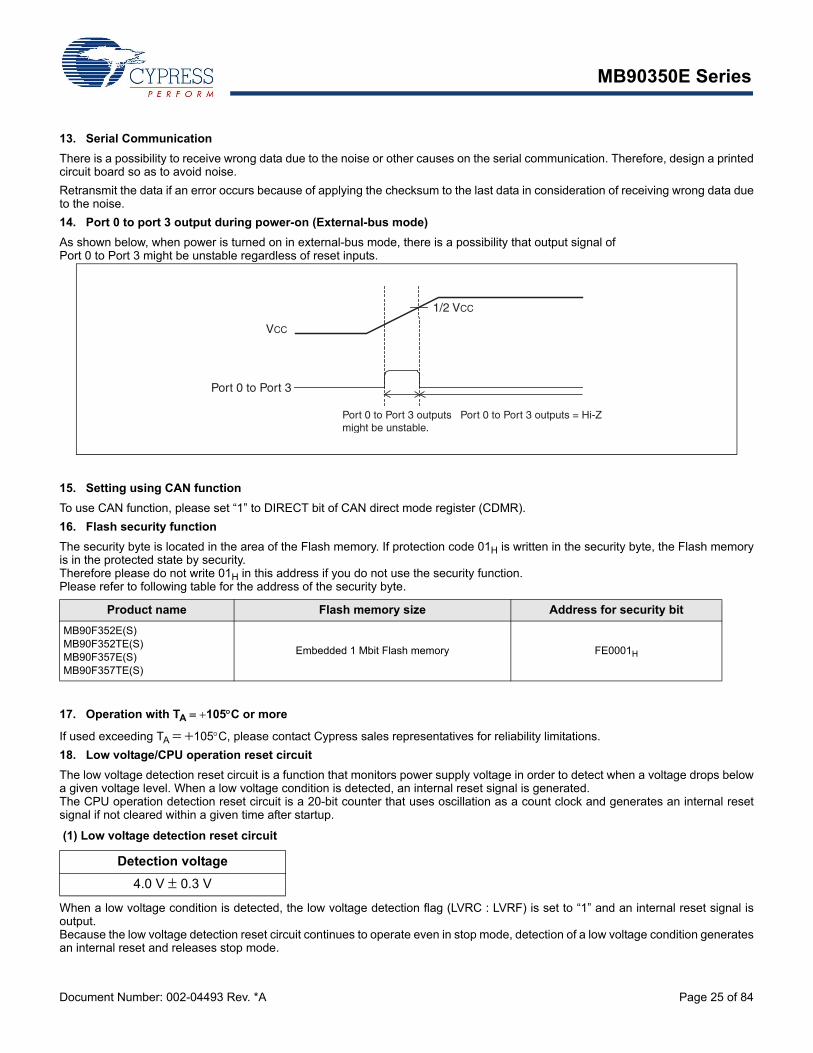
14. Port 0 to port 3 output during power-on (External-bus mode)
As shown below, when power is turned on in external-bus mode, there is a possibility that output signal of Port 0 to Port 3 might be unstable regardless of reset inputs.
15. Setting using CAN function
To use CAN function, please set “1” to DIRECT bit of CAN direct mode register (CDMR).
16. Flash security function
The security byte is located in the area of the Flash memory. If protection code 01H is written in the security byte, the Flash memoryis in the protected state by security.Therefore please do not write 01H in this address if you do not use the security function.Please refer to following table for the address of the security byte.
17. Operation with TA 105C or more
If used exceeding TA 105C, please contact Cypress sales representatives for reliability limitations.
18. Low voltage/CPU operation reset circuit
The low voltage detection reset circuit is a function that monitors power supply voltage in order to detect when a voltage drops belowa given voltage level. When a low voltage condition is detected, an internal reset signal is generated.The CPU operation detection reset circuit is a 20-bit counter that uses oscillation as a count clock and generates an internal resetsignal if not cleared within a given time after startup.
(1) Low voltage detection reset circuit
When a low voltage condition is detected, the low voltage detection flag (LVRC : LVRF) is set to “1” and an internal reset signal isoutput. Because the low voltage detection reset circuit continues to operate even in stop mode, detection of a low voltage condition generatesan internal reset and releases stop mode.
Product name Flash memory size Address for security bit
MB90F352E(S)MB90F352TE(S)MB90F357E(S)MB90F357TE(S)
Embedded 1 Mbit Flash memory FE0001H
Detection voltage
4.0 V 0.3 V
Port 0 to Port 3
Port 0 to Port 3 outputsmight be unstable.
Port 0 to Port 3 outputs = Hi-Z
VCC
1/2 VCC
MB90350E Series
Document Number: 002-04493 Rev. *A Page 26 of 84
During an internal RAM write cycle, low voltage reset is generated after the completion of writing. During the output of this internalreset, the reset output from the low voltage detection reset circuit is suppressed.
(2) CPU operation detection reset circuit
The CPU operation detection reset circuit is a counter that prevents program runaway. The counter starts automatically after apower-on reset, and must be continually and regularly cleared within a given time. If the given time interval elapses and the counterhas not been cleared, a cause such as infinite program looping is assumed and an internal reset signal is generated. The internalreset generated from the CPU operation detection circuit has a width of 5 machine cycles.
* : This value assumes the interval time at an oscillation clock frequency of 4 MHz. During recovery from standby mode, the detection period is the maximum interval plus 20 s.
This circuit does not operate in modes where CPU operation is stopped.The CPU operation detection reset circuit counter is cleared under any of the following conditions.
■“0” writing to CL bit of LVRC register
■Internal reset
■Main oscillation clock stop
■Transit to sleep mode
■Transit to timebase timer mode and watch mode
19. Internal CR oscillation circuit
Interval time
220/FC (approx. 262 ms*)
Parameter SymbolValue
UnitMin Typ Max
Oscillation frequency fRC 50 100 200 kHz
Oscillation stabilization wait time tstab 100 s
MB90350E Series
Document Number: 002-04493 Rev. *A Page 27 of 84
8. Block Diagrams
■ MB90V340E-101/102
AVCC
SCL0,SCL1
SDA0,SDA1
PPGF to PPG0
DA00,DA01
ADTG
AVRHAVRL
AN23 to AN0
AVSS
SIN4 to SIN0
SCK4 to SCK0
SOT4 to SOT0
X0X0A*
FRCK0
IN7 to IN0
OUT7 to OUT0
FRCK1
RX2 to RX0
TX2 to TX0
TIN3 to TIN0
TOT3 to TOT0
AD15 to AD00
A21 to A16
ALE
RD
WR/WRL
WRH
HRQ
HAK
RDY
CLK
INT15 to INT8
INT7 to INT0
CKOT
(INT11R to INT9R)
RSTX1
X1A*
Clock controller
RAM 30 Kbytes
Prescaler 5 channels
LIN-UART5 channels
Free-run timer 0
Input capture
8 channels
Output compare
8 channels
Free-run timer 1
CANcontroller
3 channels
16-bit reload timer 4 channels8/10-bit
A/D converter
24 channels
10-bit D/A
converter 2 channels
8/16-bitPPG
16/8 channels
I2C interface 2 channels
DTP/External interrupt
External bus
interface
F2 M
C-1
6LX
Bus
* : MB90V340E-102 only
Clock monitor
DMAC
F2MC-16LX CPU
MB90350E Series
Document Number: 002-04493 Rev. *A Page 28 of 84
■ MB90V340E-103/104
AVCC
SCL1, SCL0
SDA1, SDA0
PPGF to PPG0
DA01, DA00
ADTG
AVRHAN23 to AN0
AVSS
SIN4 to SIN0SCK4 to SCK0SOT4 to SOT0
X0X0A*
FRCK0
IN7 to IN0
OUT7 to OUT0
FRCK1
RX2 to RX0TX2 to TX0
TIN3 to TIN0TOT3 to TOT0
AD15 to AD00A23 to A16ALE
HRQ
RDYCLK
INT15 to INT8(INT15R to INT8R)
RST
DMA
HAK
WRHWRLRD
AVRL
CKOT
INT7 to INT0
X1X1A*
Clock control-
ler/Monitor
CR oscillation circuit
LIN-UART5 channels
Free-run timer 0
Input capture
8 channelsOutput
compare 8 channels
Free-run timer 1
CANcontroller
3 channels
16-bit reload timer
4 channels
8/10-bitA/D
converter 24 channels
10-bit D/A
converter 2 channels
8/16-bitPPG
16/8 channels
I2C interface 2 channels DTP/External
interrupt
External bus
interface
F2 M
C-1
6LX
Bu
s
* : MB90V340E-104 only
Clock monitor
RAM 30 Kbytes
Prescaler 5 channels
F2MC-16LXCPU
MB90350E Series
Document Number: 002-04493 Rev. *A Page 29 of 84
■ MB90351E (S) , MB90351TE (S) , MB90F351E (S) , MB90F351TE (S) , MB90352E (S) , MB90352TE (S) , MB90F352E (S) MB90F352TE (S)
AVCC
SCL0
SDA0
PPG6, PPG4PPGF to PPG8
ADTG
AVRH
AN14 to AN0
AVSS
SIN3, SIN2
SCK3, SCK2
SOT3, SOT2
FRCK0
IN7 to IN4,IN1, IN0
OUT7 to OUT4
FRCK1
RX1
TX1
TIN3, TIN1
TOT3, TOT1
AD15 to AD00
A21 to A16
ALE
RD
WR/WRL
WRHHRQ
HAK
RDY
CLK
INT15 to INT8
(INT11R to INT9DMAC
X0X0A *1
RSTX1
X1A*1
Clock controller
Low voltage/CPU operation
detection reset*2
Prescaler 2 channels
LIN-UART2 channels
Free-run timer 0
Input capture
6 channels
Output compare
4 channels
Free-run timer 1
CANcontroller 1 channel
16-bit reload timer 2 channels8/10-bit
A/D converter
15 channels
8/16-bitPPG
10/6 channels
I2C interface 1 channel
DTP/External interrupt
External bus
interface
F2 M
C-1
6LX
Bus
*1 : Only for devices without “S”-suffix*2 : Only for devices with “T”-suffix
RAM 4 Kbytes
ROM/Flash 128 Kbytes/64 Kbytes
F2MC-16LX CPU
MB90350E Series
Document Number: 002-04493 Rev. *A Page 30 of 84
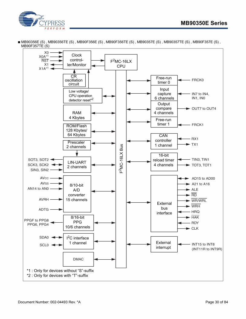
■ MB90356E (S) , MB90356TE (S) , MB90F356E (S) , MB90F356TE (S) , MB90357E (S) , MB90357TE (S) , MB90F357E (S) , MB90F357TE (S)
AVCC
SCL0
SDA0
PPG6, PPG4PPGF to PPG8
ADTG
AVRH
AN14 to AN0
AVSS
SIN3, SIN2
SCK3, SCK2
SOT3, SOT2
X0X0A*1
RST
FRCK0
IN7 to IN4,IN1, IN0
OUT7 to OUT4
FRCK1
RX1
TX1
TIN3, TIN1
TOT3, TOT1
AD15 to AD00
A21 to A16
ALE
RD
WR/WRL
WRH
HRQ
HAK
RDY
CLK
INT15 to INT8(INT11R to INT9R)
DMAC
X1X1A*1
Clock control-
ler/Monitor
CR oscillation
circuit
Prescaler 2 channels
LIN-UART2 channels
Free-run timer 0
Input capture
6 channels
Output compare
4 channels
Free-run timer 1
CANcontroller 1 channel
16-bit reload timer 4 channels
8/10-bitA/D
converter 15 channels
8/16-bitPPG
10/6 channels
I2C interface 1 channel External
interrupt
External bus
interface
F2 M
C-1
6LX
Bus
*1 : Only for devices without “S”-suffix*2 : Only for devices with “T”-suffix
RAM 4 Kbytes
ROM/Flash 128 Kbytes/64 Kbytes
Low voltage/CPU operation detector reset*2
F2MC-16LX CPU
MB90350E Series
Document Number: 002-04493 Rev. *A Page 31 of 84
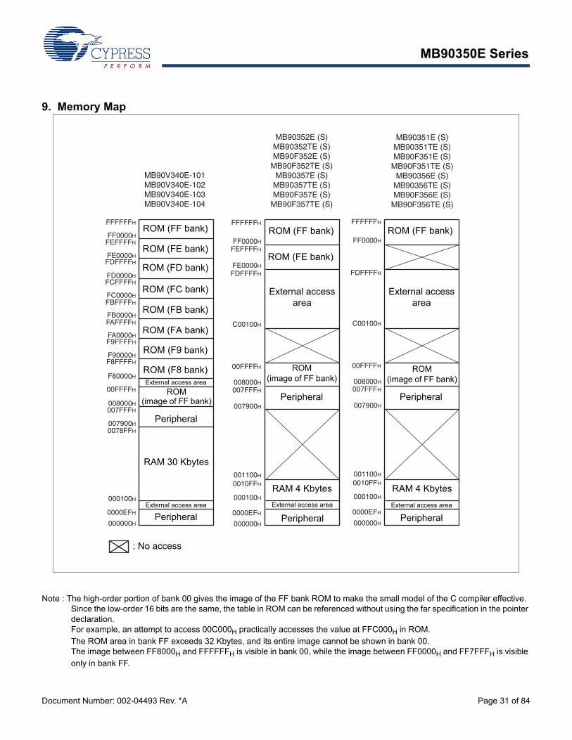
9. Memory Map
Note : The high-order portion of bank 00 gives the image of the FF bank ROM to make the small model of the C compiler effective. Since the low-order 16 bits are the same, the table in ROM can be referenced without using the far specification in the pointer declaration.For example, an attempt to access 00C000H practically accesses the value at FFC000H in ROM.
The ROM area in bank FF exceeds 32 Kbytes, and its entire image cannot be shown in bank 00.The image between FF8000H and FFFFFFH is visible in bank 00, while the image between FF0000H and FF7FFFH is visible
only in bank FF.
MB90351E (S)MB90351TE (S)MB90F351E (S)
MB90F351TE (S)MB90356E (S)
MB90356TE (S)MB90F356E (S)
MB90F356TE (S)
MB90352E (S)MB90352TE (S)MB90F352E (S)
MB90F352TE (S)MB90357E (S)
MB90357TE (S)MB90F357E (S)
MB90F357TE (S)
MB90V340E-101MB90V340E-102MB90V340E-103MB90V340E-104
FFFFFFH
F90000H
F9FFFFHFA0000H
FAFFFFHFB0000H
FBFFFFHFC0000H
FCFFFFHFD0000H
FDFFFFHFE0000H
FEFFFFHFF0000H
F8FFFFH
F80000H
00FFFFH
008000H007FFFH
007900H0078FFH
000100H
0000EFH
000000H
FFFFFFH
C00100H
FDFFFFH
FE0000H
FEFFFFHFF0000H
00FFFFH
007FFFH008000H
007900H
001100H
0010FFH
000100H
0000EFH
000000H
FFFFFFH
C00100H
FDFFFFH
FF0000H
00FFFFH
007FFFH008000H
007900H
001100H
0010FFH
000100H
0000EFH
000000H
ROM (FF bank)
ROM (FE bank)
ROM (FD bank)
ROM (FC bank)
ROM (FB bank)
ROM (FA bank)
ROM (F9 bank)
ROM (F8 bank)
ROM (image of FF bank)
Peripheral
RAM 30 Kbytes
ROM (FF bank)
ROM (FE bank)
External access area
RAM 4 Kbytes
ROM (FF bank)
Peripheral Peripheral
ROM (image of FF bank)
Peripheral
External access area
External access area
ROM (image of FF bank)
Peripheral
RAM 4 Kbytes
External access area
Peripheral
: No access
External access area
External access area
MB90350E Series
Document Number: 002-04493 Rev. *A Page 32 of 84
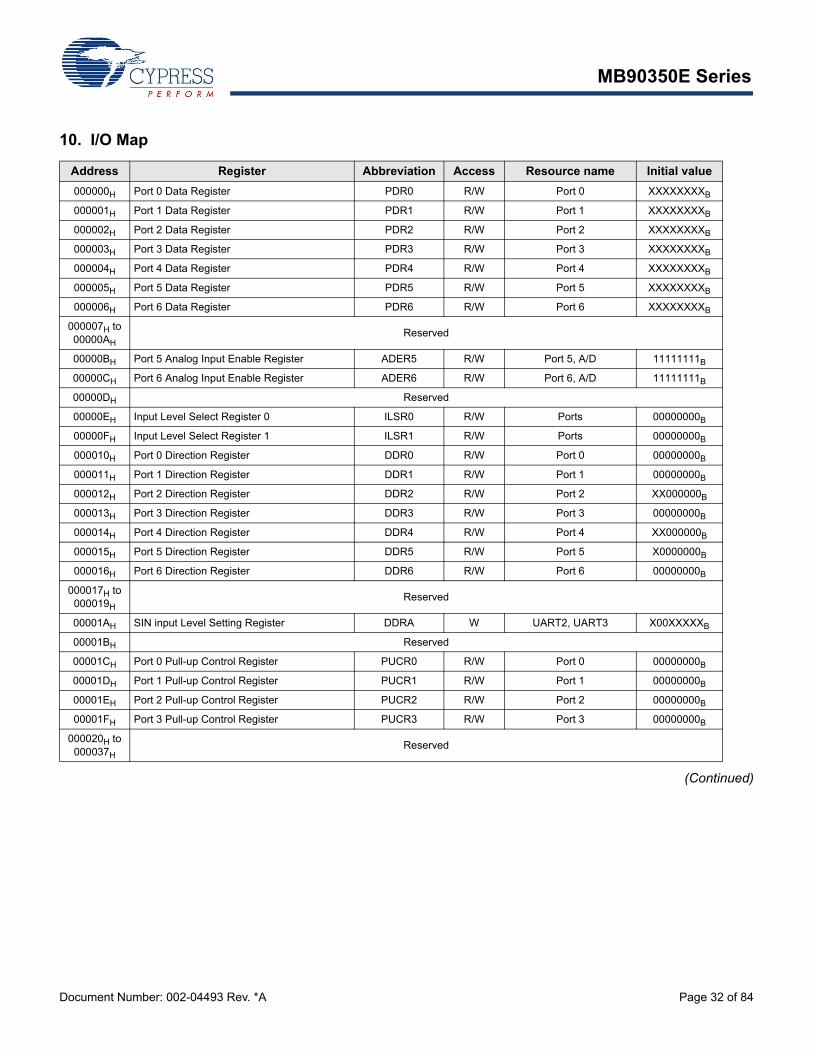
10. I/O Map
(Continued)
Address Register Abbreviation Access Resource name Initial value
000000H Port 0 Data Register PDR0 R/W Port 0 XXXXXXXXB
000001H Port 1 Data Register PDR1 R/W Port 1 XXXXXXXXB
000002H Port 2 Data Register PDR2 R/W Port 2 XXXXXXXXB
000003H Port 3 Data Register PDR3 R/W Port 3 XXXXXXXXB
000004H Port 4 Data Register PDR4 R/W Port 4 XXXXXXXXB
000005H Port 5 Data Register PDR5 R/W Port 5 XXXXXXXXB
000006H Port 6 Data Register PDR6 R/W Port 6 XXXXXXXXB
000007H to 00000AH
Reserved
00000BH Port 5 Analog Input Enable Register ADER5 R/W Port 5, A/D 11111111B
00000CH Port 6 Analog Input Enable Register ADER6 R/W Port 6, A/D 11111111B
00000DH Reserved
00000EH Input Level Select Register 0 ILSR0 R/W Ports 00000000B
00000FH Input Level Select Register 1 ILSR1 R/W Ports 00000000B
000010H Port 0 Direction Register DDR0 R/W Port 0 00000000B
000011H Port 1 Direction Register DDR1 R/W Port 1 00000000B
000012H Port 2 Direction Register DDR2 R/W Port 2 XX000000B
000013H Port 3 Direction Register DDR3 R/W Port 3 00000000B
000014H Port 4 Direction Register DDR4 R/W Port 4 XX000000B
000015H Port 5 Direction Register DDR5 R/W Port 5 X0000000B
000016H Port 6 Direction Register DDR6 R/W Port 6 00000000B
000017H to 000019H
Reserved
00001AH SIN input Level Setting Register DDRA W UART2, UART3 X00XXXXXB
00001BH Reserved
00001CH Port 0 Pull-up Control Register PUCR0 R/W Port 0 00000000B
00001DH Port 1 Pull-up Control Register PUCR1 R/W Port 1 00000000B
00001EH Port 2 Pull-up Control Register PUCR2 R/W Port 2 00000000B
00001FH Port 3 Pull-up Control Register PUCR3 R/W Port 3 00000000B
000020H to 000037H
Reserved
MB90350E Series
Document Number: 002-04493 Rev. *A Page 33 of 84
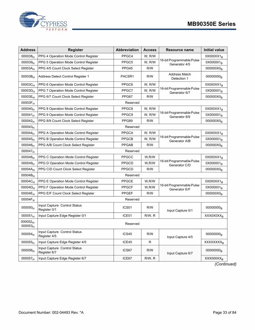
(Continued)
Address Register Abbreviation Access Resource name Initial value
000038H PPG 4 Operation Mode Control Register PPGC4 W, R/W16-bit Programmable Pulse
Generator 4/5
0X000XX1B
000039H PPG 5 Operation Mode Control Register PPGC5 W, R/W 0X000001B
00003AH PPG 4/5 Count Clock Select Register PPG45 R/W 000000X0B
00003BH Address Detect Control Register 1 PACSR1 R/WAddress Match
Detection 100000000B
00003CH PPG 6 Operation Mode Control Register PPGC6 W, R/W16-bit Programmable Pulse
Generator 6/7
0X000XX1B
00003DH PPG 7 Operation Mode Control Register PPGC7 W, R/W 0X000001B
00003EH PPG 6/7 Count Clock Select Register PPG67 R/W 000000X0B
00003FH Reserved
000040H PPG 8 Operation Mode Control Register PPGC8 W, R/W16-bit Programmable Pulse
Generator 8/9
0X000XX1B
000041H PPG 9 Operation Mode Control Register PPGC9 W, R/W 0X000001B
000042H PPG 8/9 Count Clock Select Register PPG89 R/W 000000X0B
000043H Reserved
000044H PPG A Operation Mode Control Register PPGCA W, R/W16-bit Programmable Pulse
Generator A/B
0X000XX1B
000045H PPG B Operation Mode Control Register PPGCB W, R/W 0X000001B
000046H PPG A/B Count Clock Select Register PPGAB R/W 000000X0B
000047H Reserved
000048H PPG C Operation Mode Control Register PPGCC W,R/W16-bit Programmable Pulse
Generator C/D
0X000XX1B
000049H PPG D Operation Mode Control Register PPGCD W,R/W 0X000001B
00004AH PPG C/D Count Clock Select Register PPGCD R/W 000000X0B
00004BH Reserved
00004CH PPG E Operation Mode Control Register PPGCE W,R/W16-bit Programmable Pulse
Generator E/F
0X000XX1B
00004DH PPG F Operation Mode Control Register PPGCF W,R/W 0X000001B
00004EH PPG E/F Count Clock Select Register PPGEF R/W 000000X0B
00004FH Reserved
000050HInput Capture Control Status Register 0/1
ICS01 R/WInput Capture 0/1
00000000B
000051H Input Capture Edge Register 0/1 ICE01 R/W, R XXX0X0XXB
000052H, 000053H
Reserved
000054HInput Capture Control Status Register 4/5
ICS45 R/WInput Capture 4/5
00000000B
000055H Input Capture Edge Register 4/5 ICE45 R XXXXXXXXB
000056HInput Capture Control Status Register 6/7
ICS67 R/WInput Capture 6/7
00000000B
000057H Input Capture Edge Register 6/7 ICE67 R/W, R XXX000XXB
MB90350E Series
Document Number: 002-04493 Rev. *A Page 34 of 84
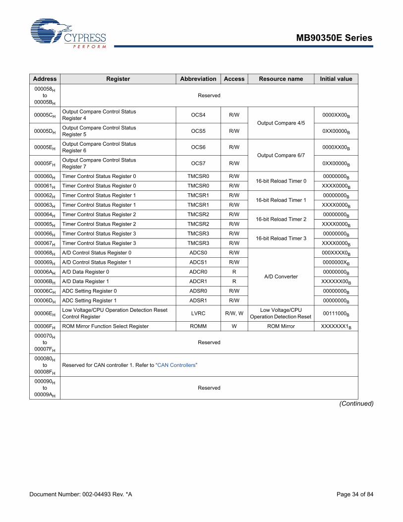
(Continued)
Address Register Abbreviation Access Resource name Initial value
000058H to
00005BH
Reserved
00005CHOutput Compare Control Status Register 4
OCS4 R/W
Output Compare 4/5
0000XX00B
00005DHOutput Compare Control Status Register 5
OCS5 R/W 0XX00000B
00005EHOutput Compare Control Status Register 6
OCS6 R/W
Output Compare 6/7
0000XX00B
00005FHOutput Compare Control Status Register 7
OCS7 R/W 0XX00000B
000060H Timer Control Status Register 0 TMCSR0 R/W16-bit Reload Timer 0
00000000B
000061H Timer Control Status Register 0 TMCSR0 R/W XXXX0000B
000062H Timer Control Status Register 1 TMCSR1 R/W16-bit Reload Timer 1
00000000B
000063H Timer Control Status Register 1 TMCSR1 R/W XXXX0000B
000064H Timer Control Status Register 2 TMCSR2 R/W16-bit Reload Timer 2
00000000B
000065H Timer Control Status Register 2 TMCSR2 R/W XXXX0000B
000066H Timer Control Status Register 3 TMCSR3 R/W16-bit Reload Timer 3
00000000B
000067H Timer Control Status Register 3 TMCSR3 R/W XXXX0000B
000068H A/D Control Status Register 0 ADCS0 R/W
A/D Converter
000XXXX0B
000069H A/D Control Status Register 1 ADCS1 R/W 0000000XB
00006AH A/D Data Register 0 ADCR0 R 00000000B
00006BH A/D Data Register 1 ADCR1 R XXXXXX00B
00006CH ADC Setting Register 0 ADSR0 R/W 00000000B
00006DH ADC Setting Register 1 ADSR1 R/W 00000000B
00006EHLow Voltage/CPU Operation Detection Reset Control Register
LVRC R/W, WLow Voltage/CPU
Operation Detection Reset 00111000B
00006FH ROM Mirror Function Select Register ROMM W ROM Mirror XXXXXXX1B
000070H to
00007FH
Reserved
000080H to
00008FH
Reserved for CAN controller 1. Refer to “CAN Controllers”
000090H to
00009AH
Reserved
MB90350E Series
Document Number: 002-04493 Rev. *A Page 35 of 84
(Continued)
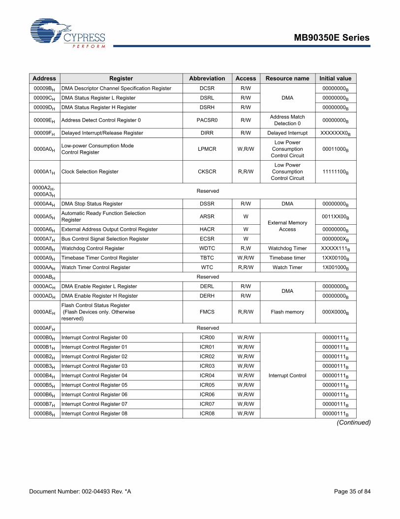
Address Register Abbreviation Access Resource name Initial value
00009BH DMA Descriptor Channel Specification Register DCSR R/W
DMA
00000000B
00009CH DMA Status Register L Register DSRL R/W 00000000B
00009DH DMA Status Register H Register DSRH R/W 00000000B
00009EH Address Detect Control Register 0 PACSR0 R/WAddress Match
Detection 000000000B
00009FH Delayed Interrupt/Release Register DIRR R/W Delayed Interrupt XXXXXXX0B
0000A0HLow-power Consumption Mode Control Register
LPMCR W,R/WLow Power
Consumption Control Circuit
00011000B
0000A1H Clock Selection Register CKSCR R,R/WLow Power
Consumption Control Circuit
11111100B
0000A2H, 0000A3H
Reserved
0000A4H DMA Stop Status Register DSSR R/W DMA 00000000B
0000A5HAutomatic Ready Function Selection Register
ARSR WExternal Memory
Access
0011XX00B
0000A6H External Address Output Control Register HACR W 00000000B
0000A7H Bus Control Signal Selection Register ECSR W 0000000XB
0000A8H Watchdog Control Register WDTC R,W Watchdog Timer XXXXX111B
0000A9H Timebase Timer Control Register TBTC W,R/W Timebase timer 1XX00100B
0000AAH Watch Timer Control Register WTC R,R/W Watch Timer 1X001000B
0000ABH Reserved
0000ACH DMA Enable Register L Register DERL R/WDMA
00000000B
0000ADH DMA Enable Register H Register DERH R/W 00000000B
0000AEH
Flash Control Status Register (Flash Devices only. Otherwise reserved)
FMCS R,R/W Flash memory 000X0000B
0000AFH Reserved
0000B0H Interrupt Control Register 00 ICR00 W,R/W
Interrupt Control
00000111B
0000B1H Interrupt Control Register 01 ICR01 W,R/W 00000111B
0000B2H Interrupt Control Register 02 ICR02 W,R/W 00000111B
0000B3H Interrupt Control Register 03 ICR03 W,R/W 00000111B
0000B4H Interrupt Control Register 04 ICR04 W,R/W 00000111B
0000B5H Interrupt Control Register 05 ICR05 W,R/W 00000111B
0000B6H Interrupt Control Register 06 ICR06 W,R/W 00000111B
0000B7H Interrupt Control Register 07 ICR07 W,R/W 00000111B
0000B8H Interrupt Control Register 08 ICR08 W,R/W 00000111B
MB90350E Series
Document Number: 002-04493 Rev. *A Page 36 of 84
(Continued)
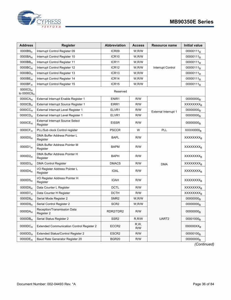
Address Register Abbreviation Access Resource name Initial value
0000B9H Interrupt Control Register 09 ICR09 W,R/W
Interrupt Control
00000111B
0000BAH Interrupt Control Register 10 ICR10 W,R/W 00000111B
0000BBH Interrupt Control Register 11 ICR11 W,R/W 00000111B
0000BCH Interrupt Control Register 12 ICR12 W,R/W 00000111B
0000BDH Interrupt Control Register 13 ICR13 W,R/W 00000111B
0000BEH Interrupt Control Register 14 ICR14 W,R/W 00000111B
0000BFH Interrupt Control Register 15 ICR15 W,R/W 00000111B
0000C0H to 0000C9H
Reserved
0000CAH External Interrupt Enable Register 1 ENIR1 R/W
External Interrupt 1
00000000B
0000CBH External Interrupt Source Register 1 EIRR1 R/W XXXXXXXXB
0000CCH External Interrupt Level Register 1 ELVR1 R/W 00000000B
0000CDH External Interrupt Level Register 1 ELVR1 R/W 00000000B
0000CEHExternal Interrupt Source Select Register
EISSR R/W 00000000B
0000CFH PLL/Sub clock Control register PSCCR W PLL XXXX0000B
0000D0HDMA Buffer Address Pointer LRegister
BAPL R/W
DMA
XXXXXXXXB
0000D1HDMA Buffer Address Pointer M Register
BAPM R/W XXXXXXXXB
0000D2HDMA Buffer Address Pointer H Register
BAPH R/W XXXXXXXXB
0000D3H DMA Control Register DMACS R/W XXXXXXXXB
0000D4HI/O Register Address Pointer L Register
IOAL R/W XXXXXXXXB
0000D5HI/O Register Address Pointer H Register
IOAH R/W XXXXXXXXB
0000D6H Data Counter L Register DCTL R/W XXXXXXXXB
0000D7H Data Counter H Register DCTH R/W XXXXXXXXB
0000D8H Serial Mode Register 2 SMR2 W,R/W
UART2
00000000B
0000D9H Serial Control Register 2 SCR2 W,R/W 00000000B
0000DAHReception/Transmission Data Register 2
RDR2/TDR2 R/W 00000000B
0000DBH Serial Status Register 2 SSR2 R,R/W 00001000B
0000DCH Extended Communication Control Register 2 ECCR2R,W,R/W
000000XXB
0000DDH Extended Status/Control Register 2 ESCR2 R/W 00000100B
0000DEH Baud Rate Generator Register 20 BGR20 R/W 00000000B
MB90350E Series
Document Number: 002-04493 Rev. *A Page 37 of 84
(Continued)
Address Register Abbreviation Access Resource name Initial value
0000DFH Baud Rate Generator Register 21 BGR21 R/W UART2 00000000B
0000E0H to 0000EFH
Reserved
0000F0H to 0000FFH
External area
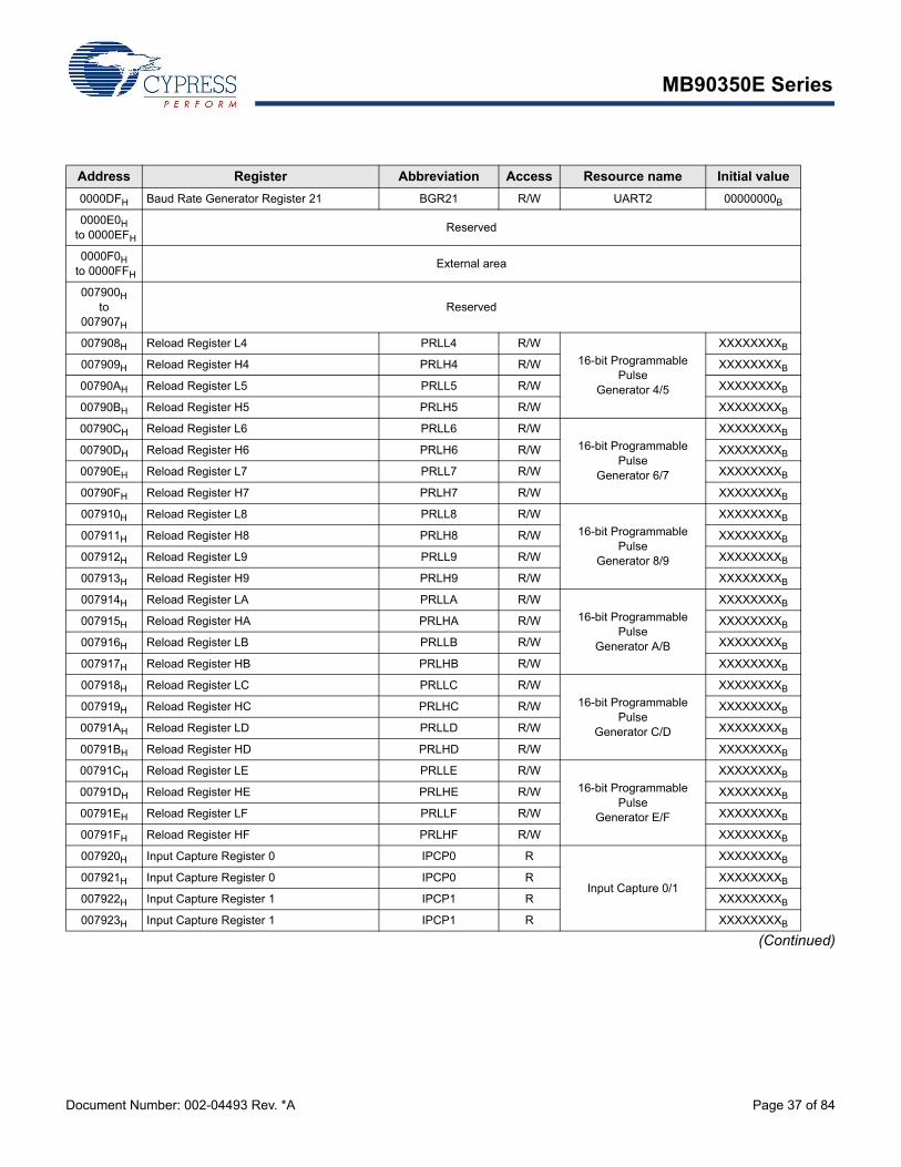
007900H to
007907H
Reserved
007908H Reload Register L4 PRLL4 R/W
16-bit Programmable Pulse
Generator 4/5
XXXXXXXXB
007909H Reload Register H4 PRLH4 R/W XXXXXXXXB
00790AH Reload Register L5 PRLL5 R/W XXXXXXXXB
00790BH Reload Register H5 PRLH5 R/W XXXXXXXXB
00790CH Reload Register L6 PRLL6 R/W
16-bit Programmable Pulse
Generator 6/7
XXXXXXXXB
00790DH Reload Register H6 PRLH6 R/W XXXXXXXXB
00790EH Reload Register L7 PRLL7 R/W XXXXXXXXB
00790FH Reload Register H7 PRLH7 R/W XXXXXXXXB
007910H Reload Register L8 PRLL8 R/W
16-bit Programmable Pulse
Generator 8/9
XXXXXXXXB
007911H Reload Register H8 PRLH8 R/W XXXXXXXXB
007912H Reload Register L9 PRLL9 R/W XXXXXXXXB
007913H Reload Register H9 PRLH9 R/W XXXXXXXXB
007914H Reload Register LA PRLLA R/W
16-bit Programmable Pulse
Generator A/B
XXXXXXXXB
007915H Reload Register HA PRLHA R/W XXXXXXXXB
007916H Reload Register LB PRLLB R/W XXXXXXXXB
007917H Reload Register HB PRLHB R/W XXXXXXXXB
007918H Reload Register LC PRLLC R/W
16-bit Programmable Pulse
Generator C/D
XXXXXXXXB
007919H Reload Register HC PRLHC R/W XXXXXXXXB
00791AH Reload Register LD PRLLD R/W XXXXXXXXB
00791BH Reload Register HD PRLHD R/W XXXXXXXXB
00791CH Reload Register LE PRLLE R/W
16-bit Programmable Pulse
Generator E/F
XXXXXXXXB
00791DH Reload Register HE PRLHE R/W XXXXXXXXB
00791EH Reload Register LF PRLLF R/W XXXXXXXXB
00791FH Reload Register HF PRLHF R/W XXXXXXXXB
007920H Input Capture Register 0 IPCP0 R
Input Capture 0/1
XXXXXXXXB
007921H Input Capture Register 0 IPCP0 R XXXXXXXXB
007922H Input Capture Register 1 IPCP1 R XXXXXXXXB
007923H Input Capture Register 1 IPCP1 R XXXXXXXXB
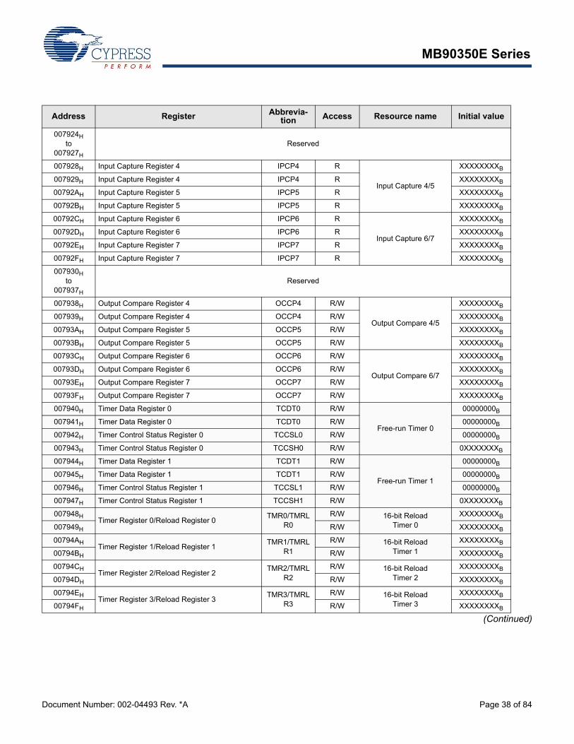
MB90350E Series
Document Number: 002-04493 Rev. *A Page 38 of 84
(Continued)
Address Register Abbrevia-tion Access Resource name Initial value
007924H to
007927H
Reserved
007928H Input Capture Register 4 IPCP4 R
Input Capture 4/5
XXXXXXXXB
007929H Input Capture Register 4 IPCP4 R XXXXXXXXB
00792AH Input Capture Register 5 IPCP5 R XXXXXXXXB
00792BH Input Capture Register 5 IPCP5 R XXXXXXXXB
00792CH Input Capture Register 6 IPCP6 R
Input Capture 6/7
XXXXXXXXB
00792DH Input Capture Register 6 IPCP6 R XXXXXXXXB
00792EH Input Capture Register 7 IPCP7 R XXXXXXXXB
00792FH Input Capture Register 7 IPCP7 R XXXXXXXXB
007930H to
007937H
Reserved
007938H Output Compare Register 4 OCCP4 R/W
Output Compare 4/5
XXXXXXXXB
007939H Output Compare Register 4 OCCP4 R/W XXXXXXXXB
00793AH Output Compare Register 5 OCCP5 R/W XXXXXXXXB
00793BH Output Compare Register 5 OCCP5 R/W XXXXXXXXB
00793CH Output Compare Register 6 OCCP6 R/W
Output Compare 6/7
XXXXXXXXB
00793DH Output Compare Register 6 OCCP6 R/W XXXXXXXXB
00793EH Output Compare Register 7 OCCP7 R/W XXXXXXXXB
00793FH Output Compare Register 7 OCCP7 R/W XXXXXXXXB
007940H Timer Data Register 0 TCDT0 R/W
Free-run Timer 0
00000000B
007941H Timer Data Register 0 TCDT0 R/W 00000000B
007942H Timer Control Status Register 0 TCCSL0 R/W 00000000B
007943H Timer Control Status Register 0 TCCSH0 R/W 0XXXXXXXB
007944H Timer Data Register 1 TCDT1 R/W
Free-run Timer 1
00000000B
007945H Timer Data Register 1 TCDT1 R/W 00000000B
007946H Timer Control Status Register 1 TCCSL1 R/W 00000000B
007947H Timer Control Status Register 1 TCCSH1 R/W 0XXXXXXXB
007948HTimer Register 0/Reload Register 0
TMR0/TMRLR0
R/W 16-bit Reload Timer 0
XXXXXXXXB
007949H R/W XXXXXXXXB
00794AHTimer Register 1/Reload Register 1
TMR1/TMRLR1
R/W 16-bit Reload Timer 1
XXXXXXXXB
00794BH R/W XXXXXXXXB
00794CHTimer Register 2/Reload Register 2
TMR2/TMRLR2
R/W 16-bit Reload Timer 2
XXXXXXXXB
00794DH R/W XXXXXXXXB
00794EHTimer Register 3/Reload Register 3
TMR3/TMRLR3
R/W 16-bit Reload Timer 3
XXXXXXXXB
00794FH R/W XXXXXXXXB
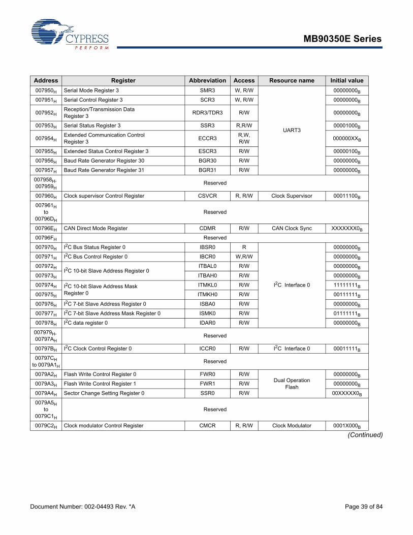
MB90350E Series
Document Number: 002-04493 Rev. *A Page 39 of 84
(Continued)
Address Register Abbreviation Access Resource name Initial value
007950H Serial Mode Register 3 SMR3 W, R/W
UART3
00000000B
007951H Serial Control Register 3 SCR3 W, R/W 00000000B
007952HReception/Transmission Data Register 3
RDR3/TDR3 R/W 00000000B
007953H Serial Status Register 3 SSR3 R,R/W 00001000B
007954HExtended Communication Control Register 3
ECCR3R,W,R/W
000000XXB
007955H Extended Status Control Register 3 ESCR3 R/W 00000100B
007956H Baud Rate Generator Register 30 BGR30 R/W 00000000B
007957H Baud Rate Generator Register 31 BGR31 R/W 00000000B
007958H, 007959H
Reserved
007960H Clock supervisor Control Register CSVCR R, R/W Clock Supervisor 00011100B
007961H to
00796DH
Reserved
00796EH CAN Direct Mode Register CDMR R/W CAN Clock Sync XXXXXXX0B
00796FH Reserved
007970H I2C Bus Status Register 0 IBSR0 R
I2C Interface 0
00000000B
007971H I2C Bus Control Register 0 IBCR0 W,R/W 00000000B
007972HI2C 10-bit Slave Address Register 0
ITBAL0 R/W 00000000B
007973H ITBAH0 R/W 00000000B
007974H I2C 10-bit Slave Address Mask Register 0
ITMKL0 R/W 11111111B
007975H ITMKH0 R/W 00111111B
007976H I2C 7-bit Slave Address Register 0 ISBA0 R/W 00000000B
007977H I2C 7-bit Slave Address Mask Register 0 ISMK0 R/W 01111111B
007978H I2C data register 0 IDAR0 R/W 00000000B
007979H, 00797AH
Reserved
00797BH I2C Clock Control Register 0 ICCR0 R/W I2C Interface 0 00011111B
00797CH to 0079A1H
Reserved
0079A2H Flash Write Control Register 0 FWR0 R/WDual Operation
Flash
00000000B
0079A3H Flash Write Control Register 1 FWR1 R/W 00000000B
0079A4H Sector Change Setting Register 0 SSR0 R/W 00XXXXX0B
0079A5H to
0079C1H
Reserved
0079C2H Clock modulator Control Register CMCR R, R/W Clock Modulator 0001X000B
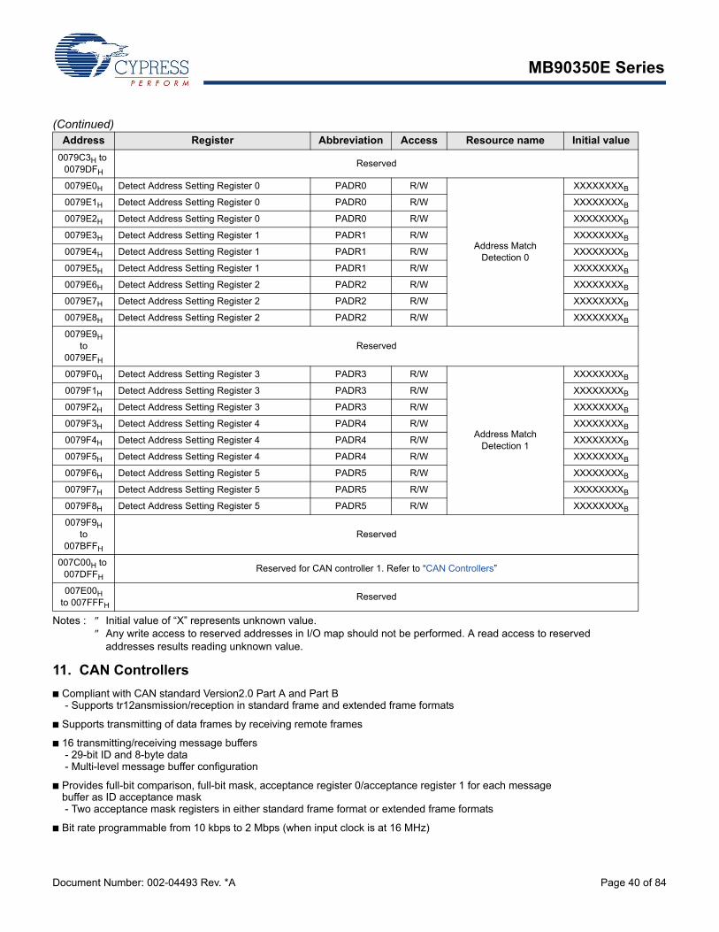
MB90350E Series
Document Number: 002-04493 Rev. *A Page 40 of 84
(Continued)
Notes : Initial value of “X” represents unknown value. Any write access to reserved addresses in I/O map should not be performed. A read access to reserved
addresses results reading unknown value.
11. CAN Controllers
■ Compliant with CAN standard Version2.0 Part A and Part B - Supports tr12ansmission/reception in standard frame and extended frame formats
■ Supports transmitting of data frames by receiving remote frames
■ 16 transmitting/receiving message buffers - 29-bit ID and 8-byte data - Multi-level message buffer configuration
■ Provides full-bit comparison, full-bit mask, acceptance register 0/acceptance register 1 for each message buffer as ID acceptance mask - Two acceptance mask registers in either standard frame format or extended frame formats
■ Bit rate programmable from 10 kbps to 2 Mbps (when input clock is at 16 MHz)
Address Register Abbreviation Access Resource name Initial value
0079C3H to 0079DFH
Reserved
0079E0H Detect Address Setting Register 0 PADR0 R/W
Address Match Detection 0
XXXXXXXXB
0079E1H Detect Address Setting Register 0 PADR0 R/W XXXXXXXXB
0079E2H Detect Address Setting Register 0 PADR0 R/W XXXXXXXXB
0079E3H Detect Address Setting Register 1 PADR1 R/W XXXXXXXXB
0079E4H Detect Address Setting Register 1 PADR1 R/W XXXXXXXXB
0079E5H Detect Address Setting Register 1 PADR1 R/W XXXXXXXXB
0079E6H Detect Address Setting Register 2 PADR2 R/W XXXXXXXXB
0079E7H Detect Address Setting Register 2 PADR2 R/W XXXXXXXXB
0079E8H Detect Address Setting Register 2 PADR2 R/W XXXXXXXXB
0079E9H to
0079EFH
Reserved
0079F0H Detect Address Setting Register 3 PADR3 R/W
Address Match Detection 1
XXXXXXXXB
0079F1H Detect Address Setting Register 3 PADR3 R/W XXXXXXXXB
0079F2H Detect Address Setting Register 3 PADR3 R/W XXXXXXXXB
0079F3H Detect Address Setting Register 4 PADR4 R/W XXXXXXXXB
0079F4H Detect Address Setting Register 4 PADR4 R/W XXXXXXXXB
0079F5H Detect Address Setting Register 4 PADR4 R/W XXXXXXXXB
0079F6H Detect Address Setting Register 5 PADR5 R/W XXXXXXXXB
0079F7H Detect Address Setting Register 5 PADR5 R/W XXXXXXXXB
0079F8H Detect Address Setting Register 5 PADR5 R/W XXXXXXXXB
0079F9H to
007BFFH
Reserved
007C00H to 007DFFH
Reserved for CAN controller 1. Refer to “CAN Controllers”
007E00H to 007FFFH
Reserved
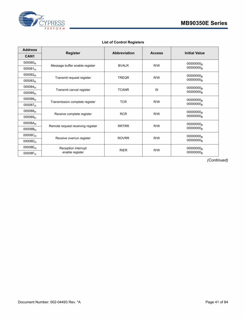
MB90350E Series
Document Number: 002-04493 Rev. *A Page 41 of 84
List of Control Registers
(Continued)
AddressRegister Abbreviation Access Initial Value
CAN1
000080HMessage buffer enable register BVALR R/W
00000000B00000000B000081H
000082HTransmit request register TREQR R/W
00000000B00000000B000083H
000084HTransmit cancel register TCANR W
00000000B 00000000B000085H
000086HTransmission complete register TCR R/W
00000000B 00000000B000087H
000088HReceive complete register RCR R/W
00000000B 00000000B000089H
00008AHRemote request receiving register RRTRR R/W
00000000B 00000000B00008BH
00008CHReceive overrun register ROVRR R/W
00000000B 00000000B00008DH
00008EH Reception interrupt enable register
RIER R/W00000000B 00000000B00008FH
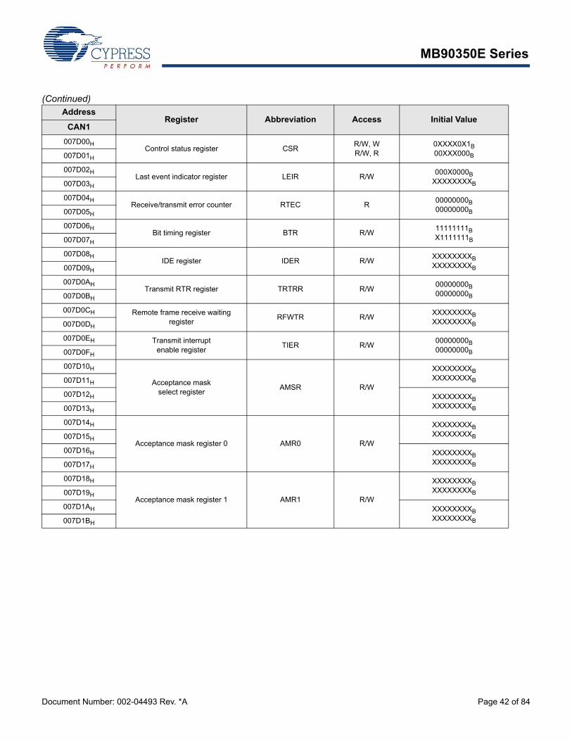
MB90350E Series
Document Number: 002-04493 Rev. *A Page 42 of 84
(Continued)Address
Register Abbreviation Access Initial ValueCAN1
007D00HControl status register CSR
R/W, WR/W, R
0XXXX0X1B00XXX000B007D01H
007D02HLast event indicator register LEIR R/W
000X0000BXXXXXXXXB007D03H
007D04HReceive/transmit error counter RTEC R
00000000B 00000000B007D05H
007D06HBit timing register BTR R/W
11111111B X1111111B007D07H
007D08HIDE register IDER R/W
XXXXXXXXB XXXXXXXXB007D09H
007D0AHTransmit RTR register TRTRR R/W
00000000B 00000000B007D0BH
007D0CH Remote frame receive waitingregister
RFWTR R/WXXXXXXXXB XXXXXXXXB007D0DH
007D0EH Transmit interrupt enable register
TIER R/W00000000B 00000000B007D0FH
007D10H
Acceptance mask select register
AMSR R/W
XXXXXXXXB XXXXXXXXB007D11H
007D12H XXXXXXXXB XXXXXXXXB007D13H
007D14H
Acceptance mask register 0 AMR0 R/W
XXXXXXXXB XXXXXXXXB007D15H
007D16H XXXXXXXXBXXXXXXXXB007D17H
007D18H
Acceptance mask register 1 AMR1 R/W
XXXXXXXXB XXXXXXXXB007D19H
007D1AH XXXXXXXXBXXXXXXXXB007D1BH
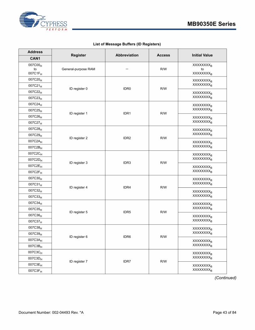
MB90350E Series
Document Number: 002-04493 Rev. *A Page 43 of 84
List of Message Buffers (ID Registers)
(Continued)
AddressRegister Abbreviation Access Initial Value
CAN1
007C00Hto
007C1FH
General-purpose RAM R/WXXXXXXXXB
toXXXXXXXXB
007C20H
ID register 0 IDR0 R/W
XXXXXXXXBXXXXXXXXB007C21H
007C22H XXXXXXXXBXXXXXXXXB007C23H
007C24H
ID register 1 IDR1 R/W
XXXXXXXXB XXXXXXXXB007C25H
007C26H XXXXXXXXB XXXXXXXXB007C27H
007C28H
ID register 2 IDR2 R/W
XXXXXXXXB XXXXXXXXB007C29H
007C2AH XXXXXXXXB XXXXXXXXB007C2BH
007C2CH
ID register 3 IDR3 R/W
XXXXXXXXB XXXXXXXXB007C2DH
007C2EH XXXXXXXXB XXXXXXXXB007C2FH
007C30H
ID register 4 IDR4 R/W
XXXXXXXXB XXXXXXXXB007C31H
007C32H XXXXXXXXB XXXXXXXXB007C33H
007C34H
ID register 5 IDR5 R/W
XXXXXXXXB XXXXXXXXB007C35H
007C36H XXXXXXXXB XXXXXXXXB007C37H
007C38H
ID register 6 IDR6 R/W
XXXXXXXXB XXXXXXXXB007C39H
007C3AH XXXXXXXXB XXXXXXXXB007C3BH
007C3CH
ID register 7 IDR7 R/W
XXXXXXXXB XXXXXXXXB007C3DH
007C3EH XXXXXXXXB XXXXXXXXB007C3FH
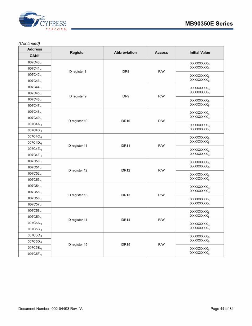
MB90350E Series
Document Number: 002-04493 Rev. *A Page 44 of 84
(Continued)Address
Register Abbreviation Access Initial ValueCAN1
007C40H
ID register 8 IDR8 R/W
XXXXXXXXB XXXXXXXXB007C41H
007C42H XXXXXXXXB XXXXXXXXB007C43H
007C44H
ID register 9 IDR9 R/W
XXXXXXXXB XXXXXXXXB007C45H
007C46H XXXXXXXXB XXXXXXXXB007C47H
007C48H
ID register 10 IDR10 R/W
XXXXXXXXBXXXXXXXXB007C49H
007C4AH XXXXXXXXB XXXXXXXXB007C4BH
007C4CH
ID register 11 IDR11 R/W
XXXXXXXXB XXXXXXXXB007C4DH
007C4EH XXXXXXXXB XXXXXXXXB007C4FH
007C50H
ID register 12 IDR12 R/W
XXXXXXXXB XXXXXXXXB007C51H
007C52H XXXXXXXXB XXXXXXXXB007C53H
007C54H
ID register 13 IDR13 R/W
XXXXXXXXB XXXXXXXXB007C55H
007C56H XXXXXXXXB XXXXXXXXB007C57H
007C58H
ID register 14 IDR14 R/W
XXXXXXXXB XXXXXXXXB007C59H
007C5AH XXXXXXXXB XXXXXXXXB007C5BH
007C5CH
ID register 15 IDR15 R/W
XXXXXXXXB XXXXXXXXB007C5DH
007C5EH XXXXXXXXB XXXXXXXXB007C5FH
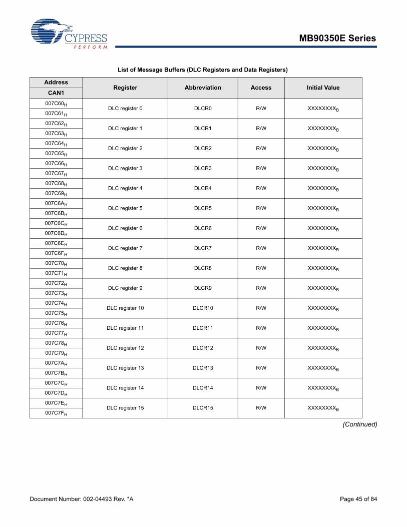
MB90350E Series
Document Number: 002-04493 Rev. *A Page 45 of 84
List of Message Buffers (DLC Registers and Data Registers)
(Continued)
AddressRegister Abbreviation Access Initial Value
CAN1
007C60HDLC register 0 DLCR0 R/W XXXXXXXXB
007C61H
007C62HDLC register 1 DLCR1 R/W XXXXXXXXB
007C63H
007C64HDLC register 2 DLCR2 R/W XXXXXXXXB
007C65H
007C66HDLC register 3 DLCR3 R/W XXXXXXXXB
007C67H
007C68HDLC register 4 DLCR4 R/W XXXXXXXXB
007C69H
007C6AHDLC register 5 DLCR5 R/W XXXXXXXXB
007C6BH
007C6CHDLC register 6 DLCR6 R/W XXXXXXXXB
007C6DH
007C6EHDLC register 7 DLCR7 R/W XXXXXXXXB
007C6FH
007C70HDLC register 8 DLCR8 R/W XXXXXXXXB
007C71H
007C72HDLC register 9 DLCR9 R/W XXXXXXXXB
007C73H
007C74HDLC register 10 DLCR10 R/W XXXXXXXXB
007C75H
007C76HDLC register 11 DLCR11 R/W XXXXXXXXB
007C77H
007C78HDLC register 12 DLCR12 R/W XXXXXXXXB
007C79H
007C7AHDLC register 13 DLCR13 R/W XXXXXXXXB
007C7BH
007C7CHDLC register 14 DLCR14 R/W XXXXXXXXB
007C7DH
007C7EHDLC register 15 DLCR15 R/W XXXXXXXXB
007C7FH
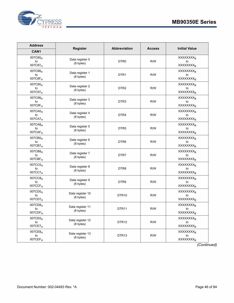
MB90350E Series
Document Number: 002-04493 Rev. *A Page 46 of 84
(Continued)
AddressRegister Abbreviation Access Initial Value
CAN1
007C80H to
007C87H
Data register 0 (8 bytes)
DTR0 R/WXXXXXXXXB
to XXXXXXXXB
007C88H to
007C8FH
Data register 1 (8 bytes)
DTR1 R/WXXXXXXXXB
to XXXXXXXXB
007C90H to
007C97H
Data register 2 (8 bytes)
DTR2 R/WXXXXXXXXB
to XXXXXXXXB
007C98H to
007C9FH
Data register 3 (8 bytes)
DTR3 R/WXXXXXXXXB
to XXXXXXXXB
007CA0H to
007CA7H
Data register 4 (8 bytes)
DTR4 R/WXXXXXXXXB
to XXXXXXXXB
007CA8H to
007CAFH
Data register 5 (8 bytes)
DTR5 R/WXXXXXXXXB
to XXXXXXXXB
007CB0H to
007CB7H
Data register 6 (8 bytes)
DTR6 R/WXXXXXXXXB
to XXXXXXXXB
007CB8H to
007CBFH
Data register 7 (8 bytes)
DTR7 R/WXXXXXXXXB
to XXXXXXXXB
007CC0H to
007CC7H
Data register 8 (8 bytes)
DTR8 R/WXXXXXXXXB
to XXXXXXXXB
007CC8H to
007CCFH
Data register 9 (8 bytes)
DTR9 R/WXXXXXXXXB
to XXXXXXXXB
007CD0H to
007CD7H
Data register 10 (8 bytes)
DTR10 R/WXXXXXXXXB
to XXXXXXXXB
007CD8H to
007CDFH
Data register 11 (8 bytes)
DTR11 R/WXXXXXXXXB
to XXXXXXXXB
007CE0H to
007CE7H
Data register 12 (8 bytes)
DTR12 R/WXXXXXXXXB
to XXXXXXXXB
007CE8H to
007CEFH
Data register 13 (8 bytes)
DTR13 R/WXXXXXXXXB
to XXXXXXXXB
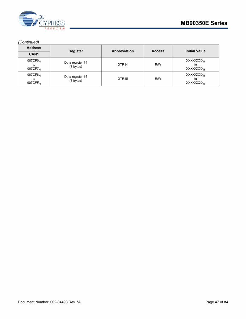
MB90350E Series
Document Number: 002-04493 Rev. *A Page 47 of 84
(Continued)Address
Register Abbreviation Access Initial ValueCAN1
007CF0H to
007CF7H
Data register 14 (8 bytes)
DTR14 R/WXXXXXXXXB
to XXXXXXXXB
007CF8H to
007CFFH
Data register 15 (8 bytes)
DTR15 R/WXXXXXXXXB
to XXXXXXXXB
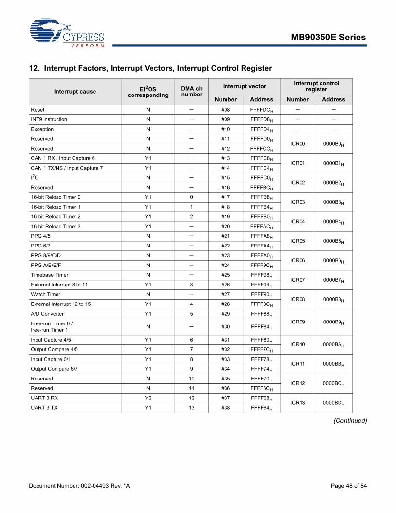
MB90350E Series
Document Number: 002-04493 Rev. *A Page 48 of 84
12. Interrupt Factors, Interrupt Vectors, Interrupt Control Register
(Continued)
Interrupt cause EI2OS corresponding
DMA ch number
Interrupt vector Interrupt control register
Number Address Number Address
Reset N #08 FFFFDCH INT9 instruction N #09 FFFFD8H Exception N #10 FFFFD4H Reserved N #11 FFFFD0H
ICR00 0000B0HReserved N #12 FFFFCCH
CAN 1 RX / Input Capture 6 Y1 #13 FFFFC8HICR01 0000B1H
CAN 1 TX/NS / Input Capture 7 Y1 #14 FFFFC4H
I2C N #15 FFFFC0HICR02 0000B2H
Reserved N #16 FFFFBCH
16-bit Reload Timer 0 Y1 0 #17 FFFFB8HICR03 0000B3H
16-bit Reload Timer 1 Y1 1 #18 FFFFB4H
16-bit Reload Timer 2 Y1 2 #19 FFFFB0HICR04 0000B4H
16-bit Reload Timer 3 Y1 #20 FFFFACH
PPG 4/5 N #21 FFFFA8HICR05 0000B5H
PPG 6/7 N #22 FFFFA4H
PPG 8/9/C/D N #23 FFFFA0HICR06 0000B6H
PPG A/B/E/F N #24 FFFF9CH
Timebase Timer N #25 FFFF98HICR07 0000B7H
External Interrupt 8 to 11 Y1 3 #26 FFFF94H
Watch Timer N #27 FFFF90HICR08 0000B8H
External Interrupt 12 to 15 Y1 4 #28 FFFF8CH
A/D Converter Y1 5 #29 FFFF88H
ICR09 0000B9HFree-run Timer 0 / free-run Timer 1
N #30 FFFF84H
Input Capture 4/5 Y1 6 #31 FFFF80HICR10 0000BAH
Output Compare 4/5 Y1 7 #32 FFFF7CH
Input Capture 0/1 Y1 8 #33 FFFF78HICR11 0000BBH
Output Compare 6/7 Y1 9 #34 FFFF74H
Reserved N 10 #35 FFFF70HICR12 0000BCH
Reserved N 11 #36 FFFF6CH
UART 3 RX Y2 12 #37 FFFF68HICR13 0000BDH
UART 3 TX Y1 13 #38 FFFF64H
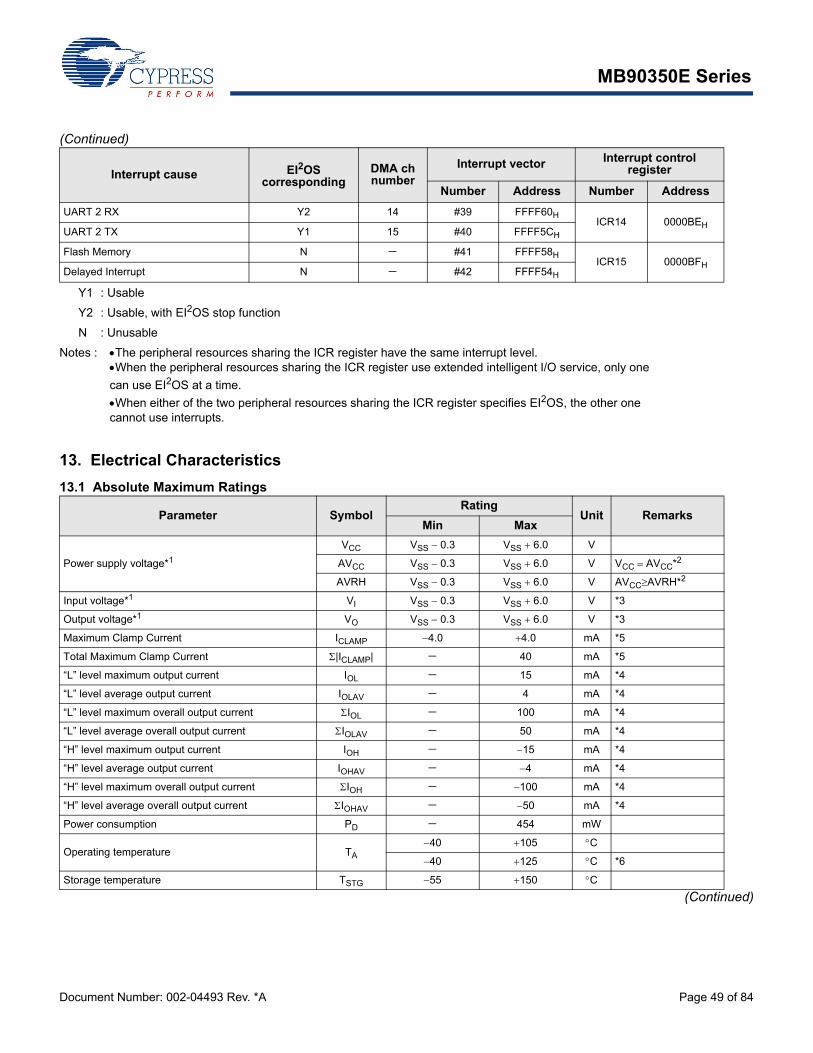
MB90350E Series
Document Number: 002-04493 Rev. *A Page 49 of 84
(Continued)
Y1 : Usable
Y2 : Usable, with EI2OS stop function
N : Unusable
Notes : The peripheral resources sharing the ICR register have the same interrupt level.When the peripheral resources sharing the ICR register use extended intelligent I/O service, only one
can use EI2OS at a time.
When either of the two peripheral resources sharing the ICR register specifies EI2OS, the other one cannot use interrupts.
13. Electrical Characteristics
13.1 Absolute Maximum Ratings
(Continued)
Interrupt cause EI2OS corresponding
DMA ch number
Interrupt vector Interrupt control register
Number Address Number Address
UART 2 RX Y2 14 #39 FFFF60HICR14 0000BEH
UART 2 TX Y1 15 #40 FFFF5CH
Flash Memory N #41 FFFF58HICR15 0000BFH
Delayed Interrupt N #42 FFFF54H
Parameter SymbolRating
Unit RemarksMin Max
Power supply voltage*1
VCC VSS 0.3 VSS 6.0 V
AVCC VSS 0.3 VSS 6.0 V VCC AVCC*2
AVRH VSS 0.3 VSS 6.0 V AVCCAVRH*2
Input voltage*1 VI VSS 0.3 VSS 6.0 V *3
Output voltage*1 VO VSS 0.3 VSS 6.0 V *3
Maximum Clamp Current ICLAMP 4.0 4.0 mA *5
Total Maximum Clamp Current |ICLAMP| 40 mA *5
“L” level maximum output current IOL 15 mA *4
“L” level average output current IOLAV 4 mA *4
“L” level maximum overall output current IOL 100 mA *4
“L” level average overall output current IOLAV 50 mA *4
“H” level maximum output current IOH 15 mA *4
“H” level average output current IOHAV 4 mA *4
“H” level maximum overall output current IOH 100 mA *4
“H” level average overall output current IOHAV 50 mA *4
Power consumption PD 454 mW
Operating temperature TA
40 105 C
40 125 C *6
Storage temperature TSTG 55 150 C
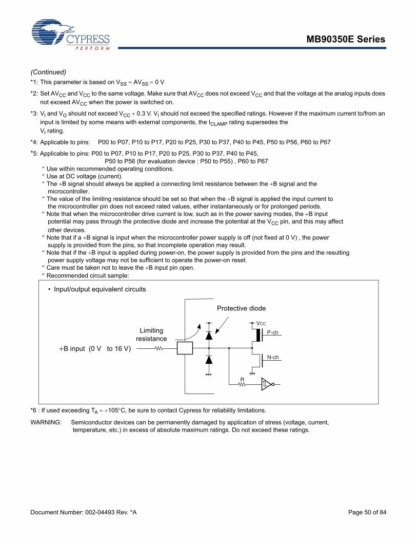
MB90350E Series
Document Number: 002-04493 Rev. *A Page 50 of 84
(Continued)
*1: This parameter is based on VSS AVSS 0 V
*2: Set AVCC and VCC to the same voltage. Make sure that AVCC does not exceed VCC and that the voltage at the analog inputs does
not exceed AVCC when the power is switched on.
*3: VI and VO should not exceed VCC 0.3 V. VI should not exceed the specified ratings. However if the maximum current to/from an
input is limited by some means with external components, the ICLAMP rating supersedes the
VI rating.
*4: Applicable to pins: P00 to P07, P10 to P17, P20 to P25, P30 to P37, P40 to P45, P50 to P56, P60 to P67
*5: Applicable to pins: P00 to P07, P10 to P17, P20 to P25, P30 to P37, P40 to P45, P50 to P56 (for evaluation device : P50 to P55) , P60 to P67
Use within recommended operating conditions. Use at DC voltage (current) The B signal should always be applied a connecting limit resistance between the B signal and the
microcontroller. The value of the limiting resistance should be set so that when the B signal is applied the input current to
the microcontroller pin does not exceed rated values, either instantaneously or for prolonged periods. Note that when the microcontroller drive current is low, such as in the power saving modes, the B input
potential may pass through the protective diode and increase the potential at the VCC pin, and this may affect
other devices. Note that if a B signal is input when the microcontroller power supply is off (not fixed at 0 V) , the power
supply is provided from the pins, so that incomplete operation may result. Note that if the B input is applied during power-on, the power supply is provided from the pins and the resulting
power supply voltage may not be sufficient to operate the power-on reset. Care must be taken not to leave the B input pin open. Recommended circuit sample:
*6 : If used exceeding TA 105C, be sure to contact Cypress for reliability limitations.
WARNING: Semiconductor devices can be permanently damaged by application of stress (voltage, current, temperature, etc.) in excess of absolute maximum ratings. Do not exceed these ratings.
P-ch
N-ch
VCC
R
• Input/output equivalent circuits
B input (0 V to 16 V)
Limitingresistance
Protective diode
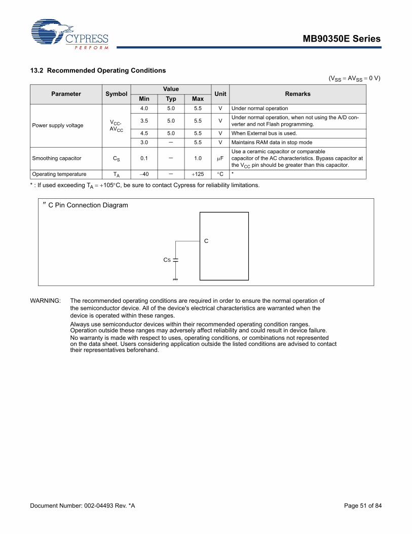
MB90350E Series
Document Number: 002-04493 Rev. *A Page 51 of 84
13.2 Recommended Operating Conditions (VSS AVSS 0 V)
* : If used exceeding TA 105C, be sure to contact Cypress for reliability limitations.
WARNING: The recommended operating conditions are required in order to ensure the normal operation of the semiconductor device. All of the device's electrical characteristics are warranted when the device is operated within these ranges.
Always use semiconductor devices within their recommended operating condition ranges. Operation outside these ranges may adversely affect reliability and could result in device failure.No warranty is made with respect to uses, operating conditions, or combinations not represented on the data sheet. Users considering application outside the listed conditions are advised to contact their representatives beforehand.
Parameter SymbolValue
Unit RemarksMin Typ Max
Power supply voltageVCC, AVCC
4.0 5.0 5.5 V Under normal operation
3.5 5.0 5.5 VUnder normal operation, when not using the A/D con-verter and not Flash programming.
4.5 5.0 5.5 V When External bus is used.
3.0 5.5 V Maintains RAM data in stop mode
Smoothing capacitor CS 0.1 1.0 FUse a ceramic capacitor or comparable capacitor of the AC characteristics. Bypass capacitor at the VCC pin should be greater than this capacitor.
Operating temperature TA 40 125 C *
C
CS
C Pin Connection Diagram
MB90350E Series
Document Number: 002-04493 Rev. *A Page 52 of 84
13.3 DC Characteristics (TA 40C to 125C, VCC 5.0 V 10, fCP 24 MHz, VSS AVSS 0 V)
(Continued)
Parameter Symbol Pin ConditionValue
Unit RemarksMin Typ Max
“H” level input voltage (At VCC 5 V 10)
VIHS 0.8 VCC VCC 0.3 V
Pin inputs if CMOS hysteresis input levels are se-lected (except P12, P15, P44, P45, P50)
VIHA 0.8 VCC VCC 0.3 VPin inputs if Automotive input levels are selected
VIHT 2.0 VCC 0.3 VPin inputs if TTL input levels are selected
VIHS 0.7 VCC VCC 0.3 VP12, P15, P50 inputs if CMOS input levels are selected
VIHI 0.7 VCC VCC 0.3 VP44, P45 inputs if CMOS hys-teresis input levels are selected
VIHR 0.8 VCC VCC 0.3 VRST input pin (CMOS hystere-sis)
VIHM VCC 0.3 VCC 0.3 V MD input pin
“L” level input voltage (At VCC 5 V 10)
VILS VSS 0.3 0.2 VCC V
Pin inputs if CMOS hysteresis input levels are se-lected (except P12, P15, P44, P45, P50)
VILA VSS 0.3 0.5 VCC VPin inputs if Automotive input levels are selected
VILT VSS 0.3 0.8 VPin inputs if TTL input levels are selected
VILS VSS 0.3 0.3 VCC VP12, P15, P50 inputs if CMOS input levels are selected
VILI VSS 0.3 0.3 VCC VP44, P45 inputs if CMOS hys-teresis input levels are selected
VILR VSS 0.3 0.2 VCC VRST input pin (CMOS hystere-sis)
VILM VSS 0.3 VSS 0.3 V MD input pin
Output “H” voltage
VOHNormal out-puts
VCC 4.5 V, IOH 4.0 mA
VCC 0.5 V
Output “H” voltage
VOHII2C current outputs
VCC 4.5 V, IOH 3.0 mA
VCC 0.5 V
MB90350E Series
Document Number: 002-04493 Rev. *A Page 53 of 84
(TA 40C to 125C, VCC 5.0 V 10, fCP 24 MHz, VSS AVSS 0 V)
(Continued)
Parameter Sym-bol Pin Condition
ValueUnit Remarks
Min Typ Max
Output “L”voltage
VOLNormal outputs
VCC 4.5 V, IOL 4.0 mA
0.4 V
Output “L” voltage
VOLII2C current outputs
VCC 4.5 V, IOL 3.0 mA
0.4 V
Input leak current
IIL VCC 5.5 V, VSS < VI < VCC
1 1 µA
Pull-up resistance
RUP
P00 to P07,P10 to P17,P20 to P25,P30 to P37,
RST
25 50 100 k
Pull-down resistance
RDOWN MD2 25 50 100 kExcept Flash memory devices
Power supply current
ICC
VCC
VCC 5.0 V, Internal frequency : 24 MHz, At normal operation.
48 60 mA
VCC 5.0 V, Internal frequency : 24 MHz, At writing Flash memory.
53 65 mAFlash memorydevices
VCC 5.0 V, Internal frequency : 24 MHz, At erasing Flash memory.
58 70 mAFlash memorydevices
ICCS
VCC 5.0 V, Internal frequency : 24 MHz, At Sleep mode.
25 35 mA
ICTS
VCC 5.0 V, Internal frequency : 2 MHz, At Main Timer mode
0.3 0.8 mADevices without “T”-suffix
0.4 1.0 mADevices with “T”-suffix
ICTSPLL
6
VCC 5.0 V, Internal frequency : 24 MHz, At PLL Timer mode, external frequency 4 MHz
4 7 mA
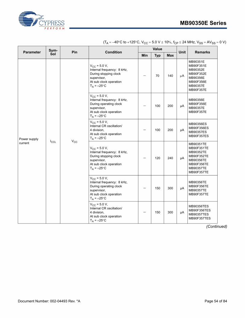
MB90350E Series
Document Number: 002-04493 Rev. *A Page 54 of 84
(TA 40C to 125C, VCC 5.0 V 10, fCP 24 MHz, VSS AVSS 0 V)
(Continued)
Parameter Sym-bol Pin Condition
ValueUnit Remarks
Min Typ Max
Power supply current
ICCL VCC
VCC = 5.0 V, Internal frequency: 8 kHz,During stopping clock supervisor,At sub clock operationTA = 25C
70 140 A
MB90351EMB90F351EMB90352EMB90F352EMB90356EMB90F356EMB90357EMB90F357E
VCC = 5.0 V, Internal frequency: 8 kHz,During operating clock supervisor,At sub clock operationTA = 25C
100 200 µA
MB90356EMB90F356EMB90357EMB90F357E
VCC = 5.0 V,Internal CR oscillation/4 division,At sub clock operationTA = 25C
100 200 µA
MB90356ESMB90F356ESMB90357ESMB90F357ES
VCC = 5.0 V, Internal frequency: 8 kHz,During stopping clock supervisor,At sub clock operationTA = 25C
120 240 µA
MB90351TEMB90F351TEMB90352TEMB90F352TEMB90356TEMB90F356TEMB90357TEMB90F357TE
VCC = 5.0 V, Internal frequency: 8 kHz,During operating clock supervisor,At sub clock operationTA = 25C
150 300 µA
MB90356TEMB90F356TEMB90357TEMB90F357TE
VCC = 5.0 V,Internal CR oscillation/4 division,At sub clock operationTA = 25C
150 300 µA
MB90356TESMB90F356TESMB90357TESMB90F357TES
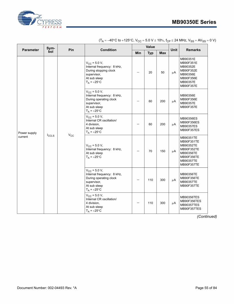
MB90350E Series
Document Number: 002-04493 Rev. *A Page 55 of 84
(TA 40C to 125C, VCC 5.0 V 10, fCP 24 MHz, VSS AVSS 0 V)
(Continued)
Parameter Sym-bol Pin Condition
ValueUnit Remarks
Min Typ Max
Power supply current
ICCLS VCC
VCC = 5.0 V, Internal frequency: 8 kHz,During stopping clock supervisor,At sub sleepTA = 25C
20 50 A
MB90351EMB90F351EMB90352EMB90F352EMB90356EMB90F356EMB90357EMB90F357E
VCC = 5.0 V, Internal frequency: 8 kHz,During operating clock supervisor,At sub sleepTA = 25C
60 200 A
MB90356EMB90F356EMB90357EMB90F357E
VCC = 5.0 V, Internal CR oscillation/4 division,At sub sleepTA = 25C
60 200 A
MB90356ESMB90F356ESMB90357ESMB90F357ES
VCC = 5.0 V, Internal frequency: 8 kHz,At sub sleepTA = 25C
70 150 A
MB90351TEMB90F351TEMB90352TEMB90F352TEMB90356TEMB90F356TEMB90357TEMB90F357TE
VCC = 5.0 V, Internal frequency: 8 kHz,During operating clock supervisor,At sub sleepTA = 25C
110 300 A
MB90356TEMB90F356TEMB90357TEMB90F357TE
VCC = 5.0 V, Internal CR oscillation/4 division,At sub sleepTA = 25C
110 300 A
MB90356TESMB90F356TESMB90357TESMB90F357TES
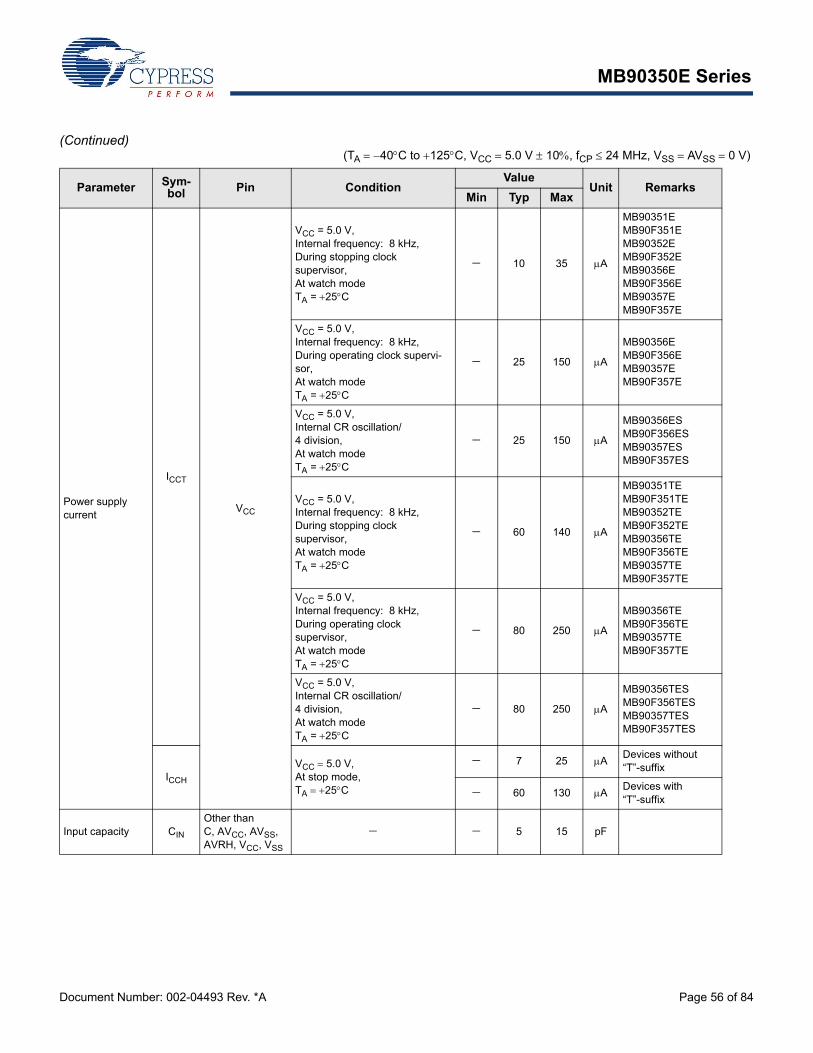
MB90350E Series
Document Number: 002-04493 Rev. *A Page 56 of 84
(Continued) (TA 40C to 125C, VCC 5.0 V 10, fCP 24 MHz, VSS AVSS 0 V)
Parameter Sym-bol Pin Condition
ValueUnit Remarks
Min Typ Max
Power supply current
ICCT
VCC
VCC = 5.0 V, Internal frequency: 8 kHz,During stopping clock supervisor,At watch modeTA = 25C
10 35 A
MB90351EMB90F351EMB90352EMB90F352EMB90356EMB90F356EMB90357EMB90F357E
VCC = 5.0 V, Internal frequency: 8 kHz,During operating clock supervi-sor, At watch modeTA = 25C
25 150 A
MB90356EMB90F356EMB90357EMB90F357E
VCC = 5.0 V, Internal CR oscillation/4 division,At watch modeTA = 25C
25 150 A
MB90356ESMB90F356ESMB90357ESMB90F357ES
VCC = 5.0 V, Internal frequency: 8 kHz,During stopping clock supervisor,At watch modeTA = 25C
60 140 A
MB90351TEMB90F351TEMB90352TEMB90F352TEMB90356TEMB90F356TEMB90357TEMB90F357TE
VCC = 5.0 V, Internal frequency: 8 kHz,During operating clock supervisor, At watch modeTA = 25C
80 250 A
MB90356TEMB90F356TEMB90357TEMB90F357TE
VCC = 5.0 V, Internal CR oscillation/4 division,At watch modeTA = 25C
80 250 A
MB90356TESMB90F356TESMB90357TESMB90F357TES
ICCH
VCC 5.0 V, At stop mode, TA 25C
7 25 ADevices without “T”-suffix
60 130 ADevices with “T”-suffix
Input capacity CIN
Other than C, AVCC, AVSS, AVRH, VCC, VSS
5 15 pF
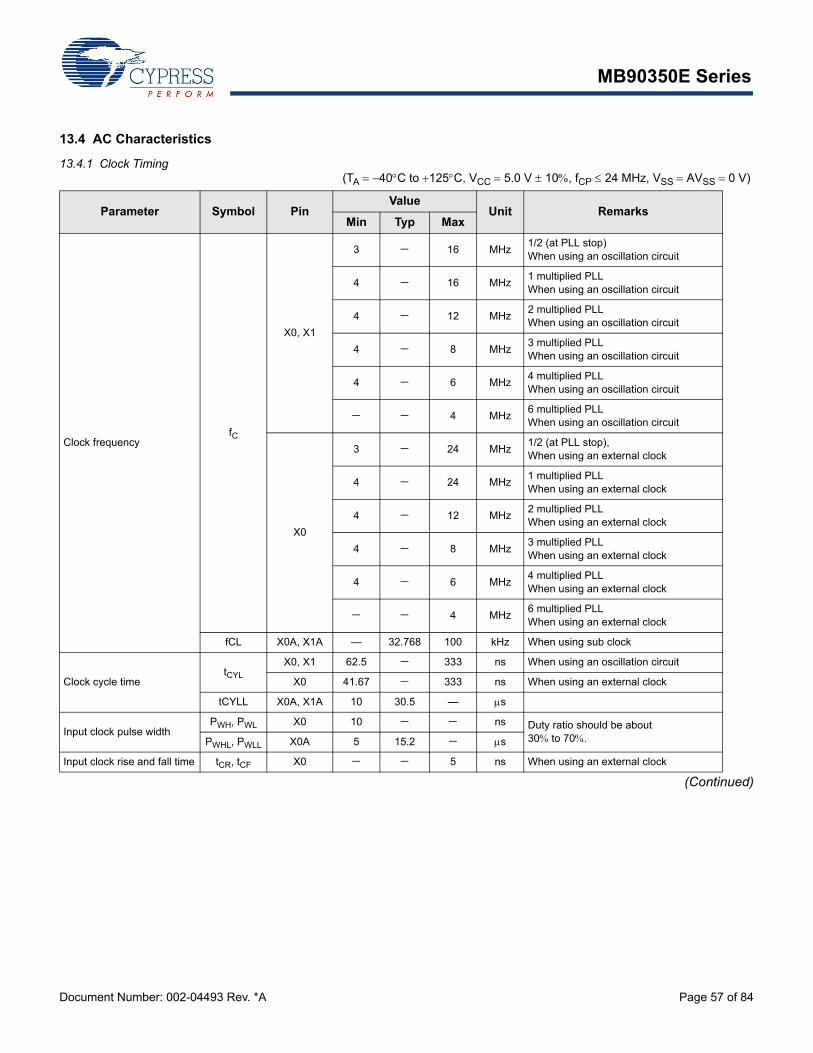
MB90350E Series
Document Number: 002-04493 Rev. *A Page 57 of 84
13.4 AC Characteristics
13.4.1 Clock Timing (TA 40C to 125C, VCC 5.0 V 10, fCP 24 MHz, VSS AVSS 0 V)
(Continued)
Parameter Symbol PinValue
Unit RemarksMin Typ Max
Clock frequencyfC
X0, X1
3 16 MHz1/2 (at PLL stop)When using an oscillation circuit
4 16 MHz1 multiplied PLLWhen using an oscillation circuit
4 12 MHz2 multiplied PLLWhen using an oscillation circuit
4 8 MHz3 multiplied PLLWhen using an oscillation circuit
4 6 MHz4 multiplied PLLWhen using an oscillation circuit
4 MHz6 multiplied PLLWhen using an oscillation circuit
X0
3 24 MHz1/2 (at PLL stop), When using an external clock
4 24 MHz1 multiplied PLLWhen using an external clock
4 12 MHz2 multiplied PLLWhen using an external clock
4 8 MHz3 multiplied PLLWhen using an external clock
4 6 MHz4 multiplied PLLWhen using an external clock
4 MHz6 multiplied PLLWhen using an external clock
fCL X0A, X1A — 32.768 100 kHz When using sub clock
Clock cycle timetCYL
X0, X1 62.5 333 ns When using an oscillation circuit
X0 41.67 333 ns When using an external clock
tCYLL X0A, X1A 10 30.5 — s
Input clock pulse widthPWH, PWL X0 10 ns Duty ratio should be about
30 to 70.PWHL, PWLL X0A 5 15.2 s
Input clock rise and fall time tCR, tCF X0 5 ns When using an external clock
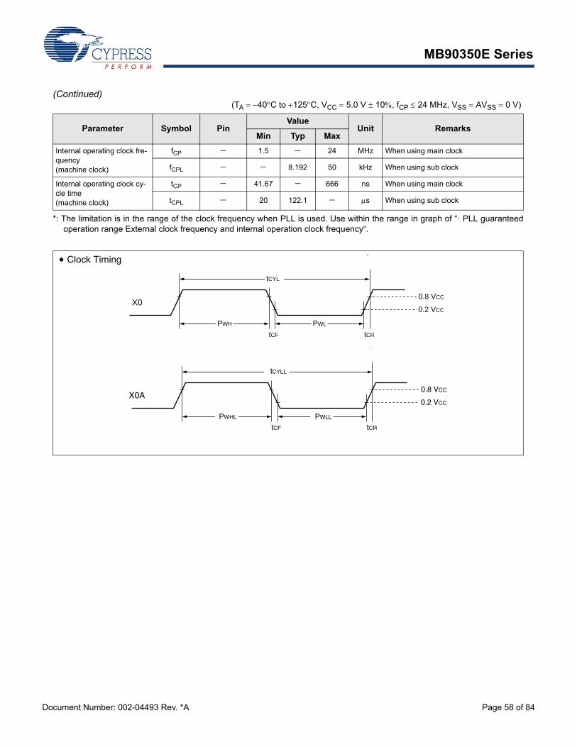
MB90350E Series
Document Number: 002-04493 Rev. *A Page 58 of 84
(Continued) (TA 40C to 125C, VCC 5.0 V 10, fCP 24 MHz, VSS AVSS 0 V)
*: The limitation is in the range of the clock frequency when PLL is used. Use within the range in graph of “· PLL guaranteedoperation range External clock frequency and internal operation clock frequency“.
Parameter Symbol PinValue
Unit RemarksMin Typ Max
Internal operating clock fre-quency (machine clock)
fCP 1.5 24 MHz When using main clock
fCPL 8.192 50 kHz When using sub clock
Internal operating clock cy-cle time (machine clock)
tCP 41.67 666 ns When using main clock
tCPL 20 122.1 s When using sub clock
X0
tCYL
tCF tCR
0.8 VCC
0.2 VCC
PWH PWL
X0A
tCYLL
tCF tCR
0.8 VCC
0.2 VCC
PWHL PWLL
Clock Timing
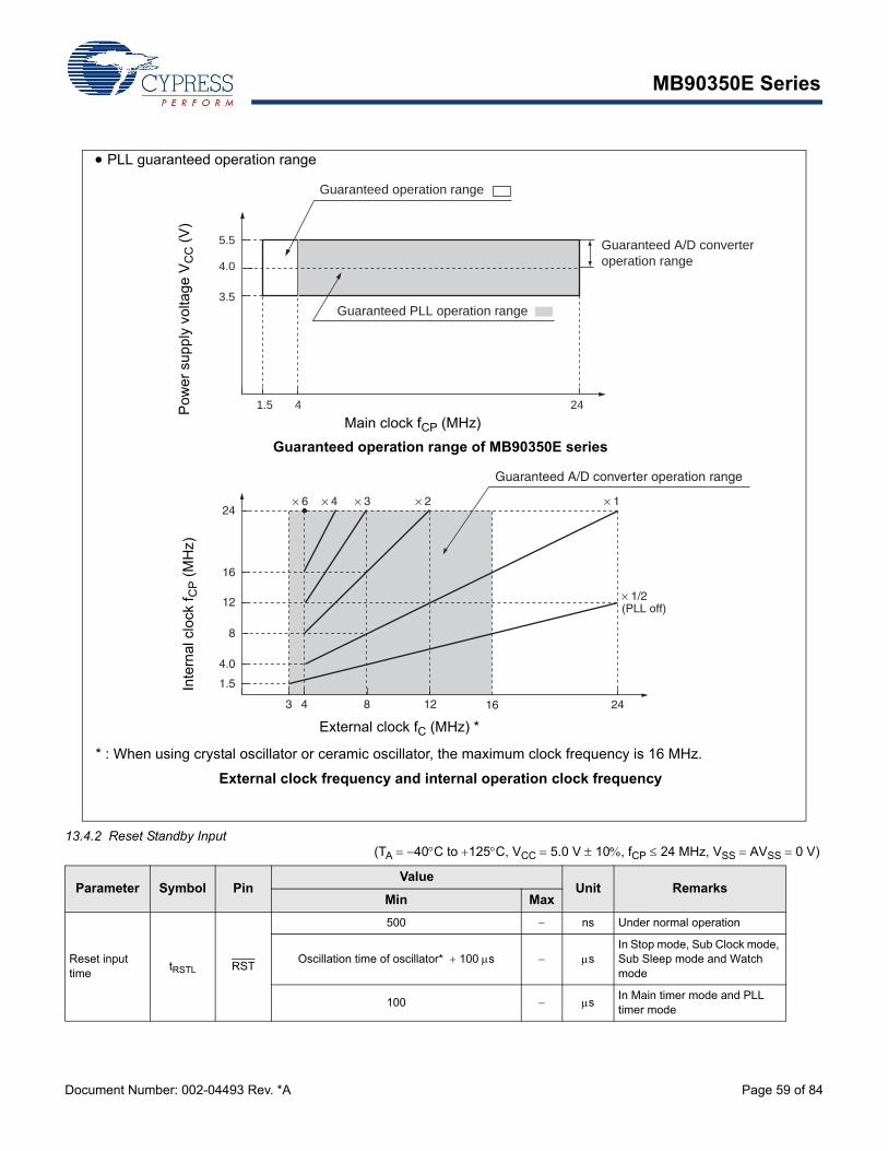
MB90350E Series
Document Number: 002-04493 Rev. *A Page 59 of 84
13.4.2 Reset Standby Input (TA 40C to 125C, VCC 5.0 V 10, fCP 24 MHz, VSS AVSS 0 V)
Parameter Symbol PinValue
Unit RemarksMin Max
Reset input time
tRSTL RST
500 ns Under normal operation
Oscillation time of oscillator* 100 s sIn Stop mode, Sub Clock mode, Sub Sleep mode and Watch mode
100 sIn Main timer mode and PLL timer mode
PLL guaranteed operation range
Guaranteed operation range of MB90350E series
* : When using crystal oscillator or ceramic oscillator, the maximum clock frequency is 16 MHz.
External clock frequency and internal operation clock frequency
5.5
3.5
41.5 24
4.0
Guaranteed A/D converteroperation range
Guaranteed PLL operation range
Guaranteed operation rangeP
ower
sup
ply
volta
ge V
CC
(V
)
Main clock fCP (MHz)
24
16
12
8
4.0
1.5
3 4 8 2412
× 1/2(PLL off)
16
Guaranteed A/D converter operation range
× 1× 2× 3× 4× 6
Inte
rnal
clo
ck f
CP (
MH
z)
External clock fC (MHz) *
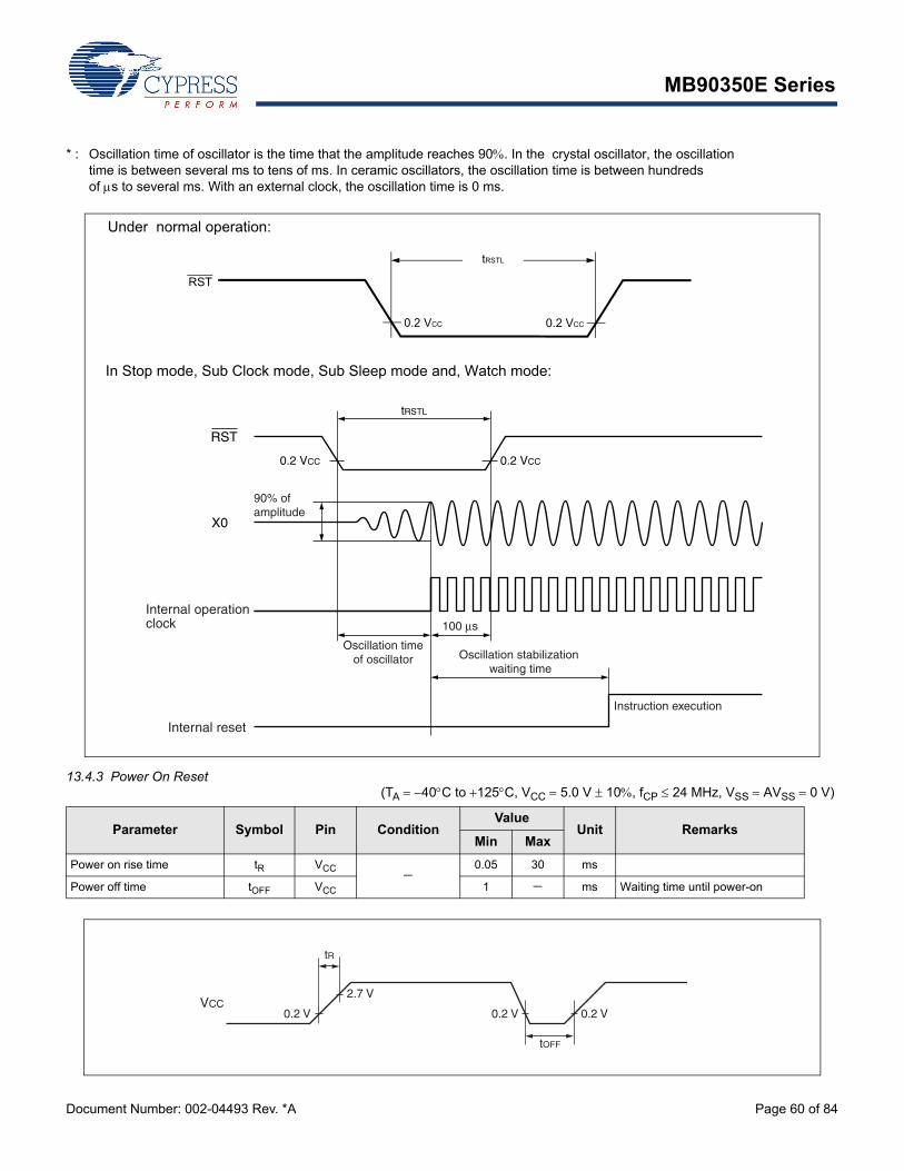
MB90350E Series
Document Number: 002-04493 Rev. *A Page 60 of 84
* : Oscillation time of oscillator is the time that the amplitude reaches 90. In the crystal oscillator, the oscillation time is between several ms to tens of ms. In ceramic oscillators, the oscillation time is between hundreds of s to several ms. With an external clock, the oscillation time is 0 ms.
13.4.3 Power On Reset (TA 40C to 125C, VCC 5.0 V 10, fCP 24 MHz, VSS AVSS 0 V)
Parameter Symbol Pin ConditionValue
Unit RemarksMin Max
Power on rise time tR VCC 0.05 30 ms
Power off time tOFF VCC 1 ms Waiting time until power-on
tRSTL
0.2 VCC 0.2 VCC
RST
X0
90% ofamplitude
Instruction execution
Oscillation stabilization waiting time
Oscillation timeof oscillator
Internal operationclock
Internal reset
100 μs
0.2 VCC
RST
tRSTL
0.2 VCC
Under normal operation:
In Stop mode, Sub Clock mode, Sub Sleep mode and, Watch mode:
VCC
tR
tOFF
2.7 V
0.2 V 0.2 V0.2 V
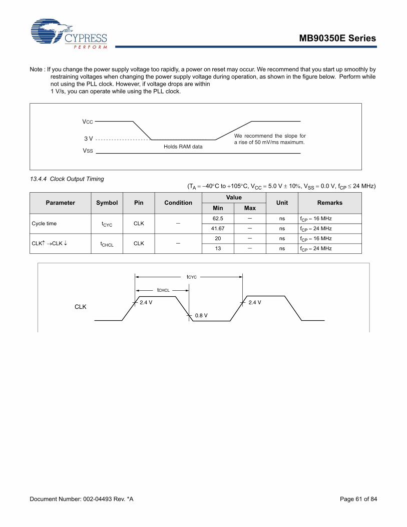
MB90350E Series
Document Number: 002-04493 Rev. *A Page 61 of 84
Note : If you change the power supply voltage too rapidly, a power on reset may occur. We recommend that you start up smoothly by restraining voltages when changing the power supply voltage during operation, as shown in the figure below. Perform while not using the PLL clock. However, if voltage drops are within 1 V/s, you can operate while using the PLL clock.
13.4.4 Clock Output Timing (TA 40C to 105C, VCC 5.0 V 10, VSS 0.0 V, fCP 24 MHz)
Parameter Symbol Pin ConditionValue
Unit RemarksMin Max
Cycle time tCYC CLK 62.5 ns fCP 16 MHz
41.67 ns fCP 24 MHz
CLK CLK tCHCL CLK 20 ns fCP 16 MHz
13 ns fCP 24 MHz
VCC
VSS
3 VHolds RAM data
We recommend the slope for a rise of 50 mV/ms maximum.
CLK2.4 V
tCYC
2.4 V
0.8 V
tCHCL
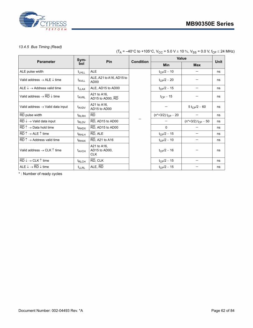
MB90350E Series
Document Number: 002-04493 Rev. *A Page 62 of 84
13.4.5 Bus Timing (Read)(TA = –40C to +105C, VCC = 5.0 V 10 , VSS = 0.0 V, fCP 24 MHz)
* : Number of ready cycles
Parameter Sym-bol Pin Condition
ValueUnit
Min Max
ALE pulse width tLHLL ALE
tCP/2 10 ns
Valid address ALE time tAVLLALE, A21 to A16, AD15 to AD00
tCP/2 20 ns
ALE Address valid time tLLAX ALE, AD15 to AD00 tCP/2 15 ns
Valid address RD time tAVRLA21 to A16, AD15 to AD00, RD
tCP 15 ns
Valid address Valid data input tAVDVA21 to A16, AD15 to AD00
5 tCP/2 60 ns
RD pulse width tRLRH RD (n*+3/2) tCP 20 ns
RD Valid data input tRLDV RD, AD15 to AD00 (n*+3/2) tCP 50 ns
RD Data hold time tRHDX RD, AD15 to AD00 0 ns
RD ALE time tRHLH RD, ALE tCP/2 15 ns
RD Address valid time tRHAX RD, A21 to A16 tCP/2 10 ns
Valid address CLK time tAVCH
A21 to A16, AD15 to AD00,CLK
tCP/2 16 ns
RD CLK time tRLCH RD, CLK tCP/2 15 ns
ALE RD time tLLRL ALE, RD tCP/2 15 ns
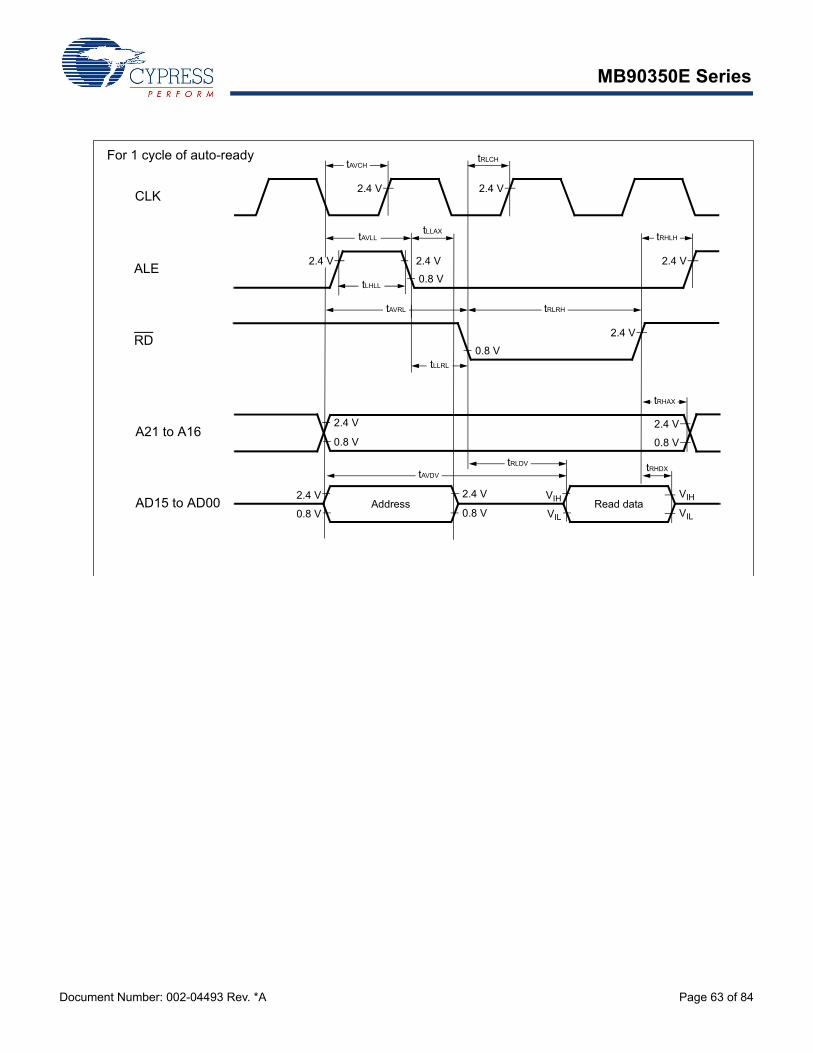
MB90350E Series
Document Number: 002-04493 Rev. *A Page 63 of 84
A21 to A160.8 V
2.4 V2.4 V
0.8 V
tRHAX
AD15 to AD000.8 V
2.4 V 2.4 V
0.8 VAddress
VIL
VIH VIH
VIL
Read data
tRHDXtRLDV
tAVDV
CLK
tAVCH
2.4 V
tRLCH
2.4 V
ALE2.4 V
tLHLL
2.4 V
tRHLH
0.8 V
tLLAX
2.4 V
tAVLL
RD
tLLRL
tRLRH
0.8 V
2.4 V
tAVRL
For 1 cycle of auto-ready
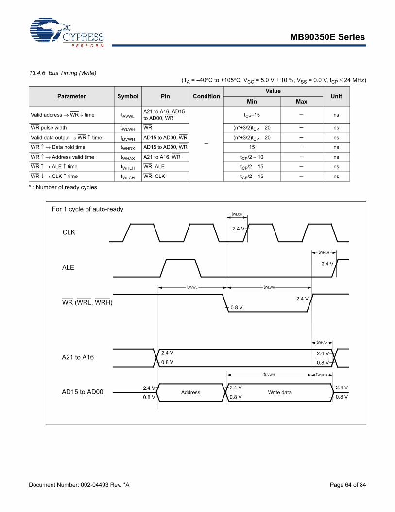
MB90350E Series
Document Number: 002-04493 Rev. *A Page 64 of 84
13.4.6 Bus Timing (Write)(TA = –40C to +105C, VCC = 5.0 V 10 , VSS = 0.0 V, fCP 24 MHz)
* : Number of ready cycles
Parameter Symbol Pin ConditionValue
UnitMin Max
Valid address WR time tAVWLA21 to A16, AD15 to AD00, WR
tCP15 ns
WR pulse width tWLWH WR (n*+3/2)tCP 20 ns
Valid data output WR time tDVWH AD15 to AD00, WR (n*+3/2)tCP 20 ns
WR Data hold time tWHDX AD15 to AD00, WR 15 ns
WR Address valid time tWHAX A21 to A16, WR tCP/2 10 ns
WR ALE time tWHLH WR, ALE tCP/2 15 ns
WR CLK time tWLCH WR, CLK tCP/2 15 ns
CLK
tWLCH
2.4 V
ALE
tWHLH
2.4 V
WR (WRL, WRH)
tWLWH
0.8 V
2.4 V
tAVWL
A21 to A160.8 V
2.4 V2.4 V
0.8 V
tWHAX
AD15 to AD002.4 V
0.8 VAddress
0.8 V
2.4 VWrite data
tDVWH
0.8 V
2.4 V
tWHDX
For 1 cycle of auto-ready
MB90350E Series
Document Number: 002-04493 Rev. *A Page 65 of 84
13.4.7 Ready Input Timing(TA = –40C to +105C, VCC = 5.0 V 10 , VSS = 0.0 V, fCP 24 MHz)
Note : If the RDY set-up time is insufficient, use the auto-ready function.
Parameter Symbol Pin ConditionValue
Units RemarksMin Max
RDY set-up time tRYHS RDY
45 ns fCP 16 MHz
32 ns fCP 24 MHz
RDY hold time tRYHH RDY 0 ns
CLK 2.4 V
ALE
RD/WR
RDY(When WAIT is not used.)
VIH VIH
tRYHH
RDY(When WAIT is used.)
tRYHS
VIL
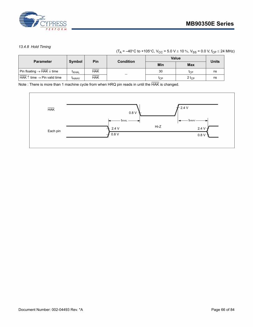
MB90350E Series
Document Number: 002-04493 Rev. *A Page 66 of 84
13.4.8 Hold Timing(TA = –40C to +105C, VCC = 5.0 V 10 , VSS = 0.0 V, fCP 24 MHz)
Note : There is more than 1 machine cycle from when HRQ pin reads in until the HAK is changed.
Parameter Symbol Pin ConditionValue
UnitsMin Max
Pin floating HAK time tXHAL HAK
30 tCP ns
HAK time Pin valid time tHAHV HAK tCP 2 tCP ns
HAK
Each pinHi-Z
tHAHVtXHAL
2.4 V
0.8 V
2.4 V 2.4 V
0.8 V 0.8 V
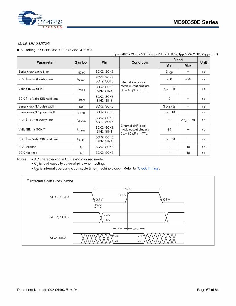
MB90350E Series
Document Number: 002-04493 Rev. *A Page 67 of 84
13.4.9 LIN-UART2/3
■ Bit setting: ESCR:SCES = 0, ECCR:SCDE = 0 (TA 40C to 125C, VCC 5.0 V 10, fCP 24 MHz, VSS 0 V)
Notes : AC characteristic in CLK synchronized mode. CL is load capacity value of pins when testing.
tCP is internal operating clock cycle time (machine clock) . Refer to “Clock Timing”.
Parameter Symbol Pin ConditionValue
UnitMin Max
Serial clock cycle time tSCYC SCK2, SCK3
Internal shift clock mode output pins are CL 80 pF 1 TTL.
5 tCP ns
SCK SOT delay time tSLOVISCK2, SCK3SOT2, SOT3
50 50 ns
Valid SIN SCK tIVSHISCK2, SCK3SIN2, SIN3
tCP + 80 ns
SCK Valid SIN hold time tSHIXISCK2, SCK3SIN2, SIN3
0 ns
Serial clock “L” pulse width tSHSL SCK2, SCK3
External shift clock mode output pins are CL 80 pF 1 TTL.
3 tCP - tR ns
Serial clock “H” pulse width tSLSH SCK2, SCK3 tCP + 10 ns
SCK SOT delay time tSLOVESCK2, SCK3SOT2, SOT3
2 tCP + 60 ns
Valid SIN SCK tIVSHESCK2, SCK3SIN2, SIN3
30 ns
SCK Valid SIN hold time tSHIXESCK2, SCK3SIN2, SIN3
tCP + 30 ns
SCK fall time tF SCK2, SCK3 10 ns
SCK rise time tR SCK2, SCK3 10 ns
SCK2, SCK3 2.4 V
0.8 V
SOT2, SOT30.8 V
2.4 V
0.8 V
tSLOVI
SIN2, SIN3VIL
VIH
VIL
VIH
tSCYC
tIVSHI tSHIXI
Internal Shift Clock Mode
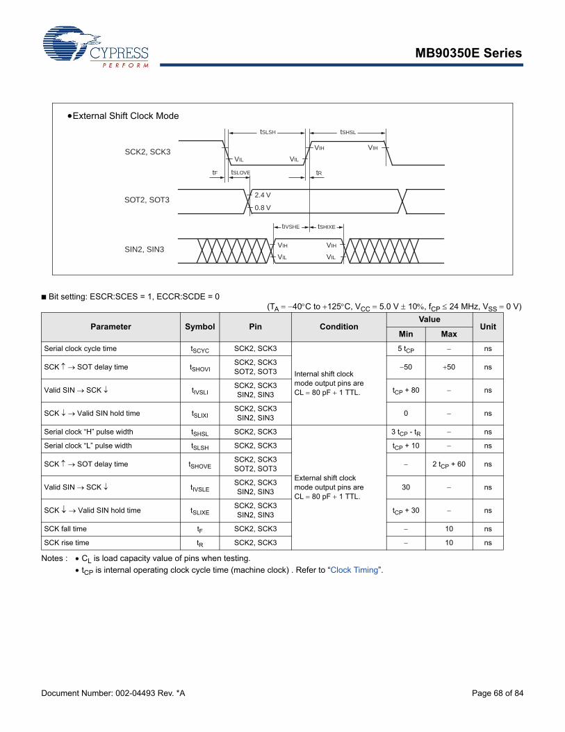
MB90350E Series
Document Number: 002-04493 Rev. *A Page 68 of 84
■ Bit setting: ESCR:SCES = 1, ECCR:SCDE = 0 (TA 40C to 125C, VCC 5.0 V 10, fCP 24 MHz, VSS 0 V)
Notes : CL is load capacity value of pins when testing.
tCP is internal operating clock cycle time (machine clock) . Refer to “Clock Timing”.
Parameter Symbol Pin ConditionValue
UnitMin Max
Serial clock cycle time tSCYC SCK2, SCK3
Internal shift clock mode output pins are CL 80 pF 1 TTL.
5 tCP ns
SCK SOT delay time tSHOVISCK2, SCK3SOT2, SOT3
50 50 ns
Valid SIN SCK tIVSLISCK2, SCK3SIN2, SIN3
tCP + 80 ns
SCK Valid SIN hold time tSLIXISCK2, SCK3SIN2, SIN3
0 ns
Serial clock “H” pulse width tSHSL SCK2, SCK3
External shift clock mode output pins are CL 80 pF 1 TTL.
3 tCP - tR ns
Serial clock “L” pulse width tSLSH SCK2, SCK3 tCP + 10 ns
SCK SOT delay time tSHOVESCK2, SCK3SOT2, SOT3
2 tCP + 60 ns
Valid SIN SCK tIVSLESCK2, SCK3SIN2, SIN3
30 ns
SCK Valid SIN hold time tSLIXESCK2, SCK3SIN2, SIN3
tCP + 30 ns
SCK fall time tF SCK2, SCK3 10 ns
SCK rise time tR SCK2, SCK3 10 ns
External Shift Clock Mode
SCK2, SCK3 VIH
VIL
SOT2, SOT30.8 V
2.4 V
tSLOVE
SIN2, SIN3VIL
VIH
VIL
VIH
VIH
VIL
tRtF
tSHSLtSLSH
tIVSHE tSHIXE
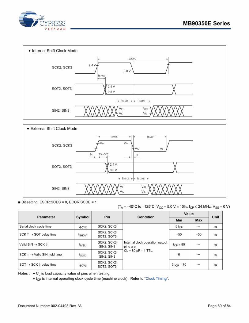
MB90350E Series
Document Number: 002-04493 Rev. *A Page 69 of 84
■ Bit setting: ESCR:SCES = 0, ECCR:SCDE = 1 (TA 40C to 125C, VCC 5.0 V 10, fCP 24 MHz, VSS 0 V)
Notes : CL is load capacity value of pins when testing.
tCP is internal operating clock cycle time (machine clock) . Refer to “Clock Timing”.
Parameter Symbol Pin ConditionValue
UnitMin Max
Serial clock cycle time tSCYC SCK2, SCK3
Internal clock operation output pins are CL 80 pF 1 TTL.
5 tCP ns
SCK SOT delay time tSHOVISCK2, SCK3SOT2, SOT3
50 50 ns
Valid SIN SCK tIVSLISCK2, SCK3SIN2, SIN3
tCP 80 ns
SCK Valid SIN hold time tSLIXISCK2, SCK3SIN2, SIN3
0 ns
SOT SCK delay time tSOVLISCK2, SCK3SOT2, SOT3
3 tCP 70 ns
Internal Shift Clock Mode
SCK2, SCK32.4 V
tSCYC
0.8 V
SOT2, SOT30.8 V
2.4 V
tSHOVI
SIN2, SIN3VIL
VIH
tIVSLI
VIL
VIH
tSLIXI
External Shift Clock Mode
SCK2, SCK3VIH
VIL
SOT2, SOT30.8 V
2.4 V
tSHOVE
SIN2, SIN3VIL
VIH
tIVSLE
VIL
VIH
tSLIXE
VIH
VIL
tSHSL
tR tF
tSLSH
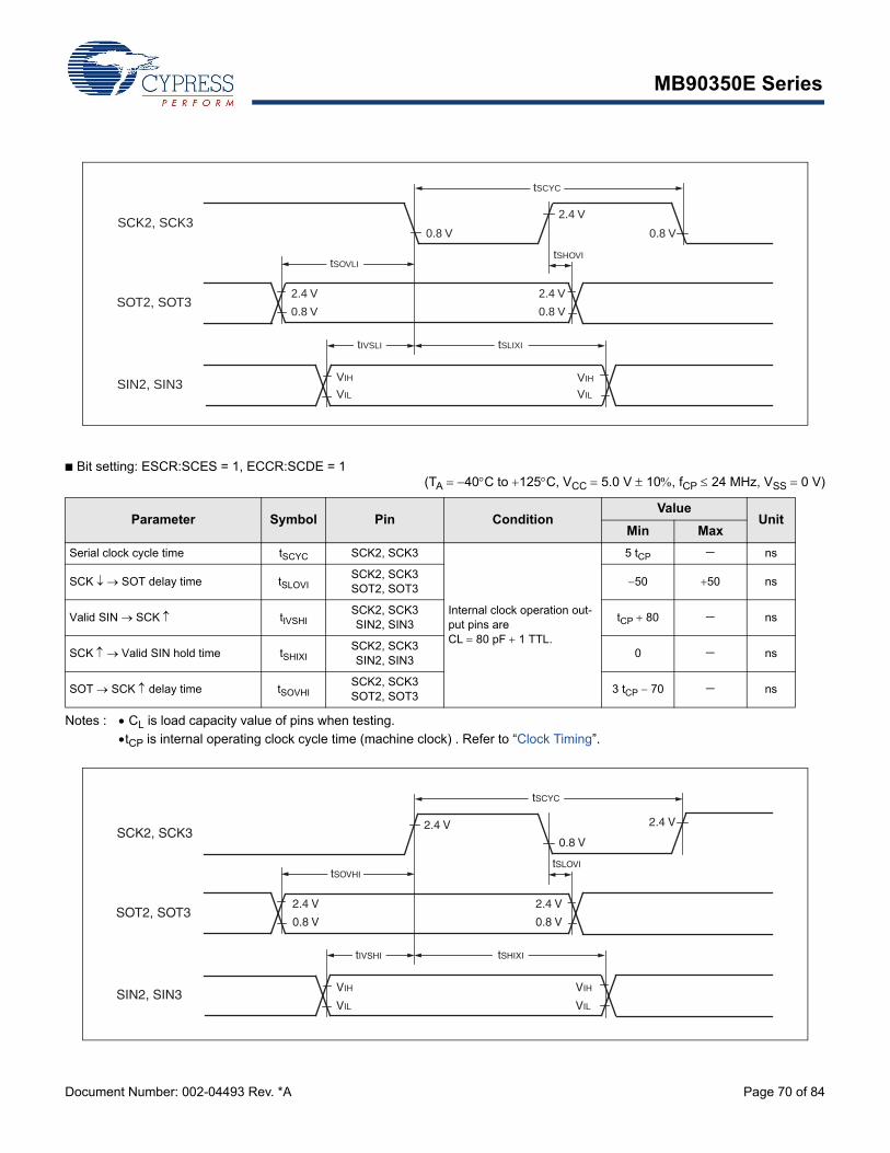
MB90350E Series
Document Number: 002-04493 Rev. *A Page 70 of 84
■ Bit setting: ESCR:SCES = 1, ECCR:SCDE = 1 (TA 40C to 125C, VCC 5.0 V 10, fCP 24 MHz, VSS 0 V)
Notes : CL is load capacity value of pins when testing.
tCP is internal operating clock cycle time (machine clock) . Refer to “Clock Timing”.
Parameter Symbol Pin ConditionValue
UnitMin Max
Serial clock cycle time tSCYC SCK2, SCK3
Internal clock operation out-put pins are CL 80 pF 1 TTL.
5 tCP ns
SCK SOT delay time tSLOVISCK2, SCK3SOT2, SOT3
50 50 ns
Valid SIN SCK tIVSHISCK2, SCK3SIN2, SIN3
tCP 80 ns
SCK Valid SIN hold time tSHIXISCK2, SCK3SIN2, SIN3
0 ns
SOT SCK delay time tSOVHISCK2, SCK3SOT2, SOT3
3 tCP 70 ns
SCK2, SCK32.4 V
tSCYC
0.8 V
SOT2, SOT30.8 V
2.4 V
tSOVLI
SIN2, SIN3VIL
VIH
tIVSLI
VIL
VIH
tSLIXI
0.8 V
tSHOVI
0.8 V
2.4 V
SCK2, SCK32.4 V
tSCYC
2.4 V
SOT2, SOT30.8 V
2.4 V
tSOVHI
SIN2, SIN3VIL
VIH
tIVSHI
VIL
VIH
tSHIXI
0.8 V
tSLOVI
0.8 V
2.4 V
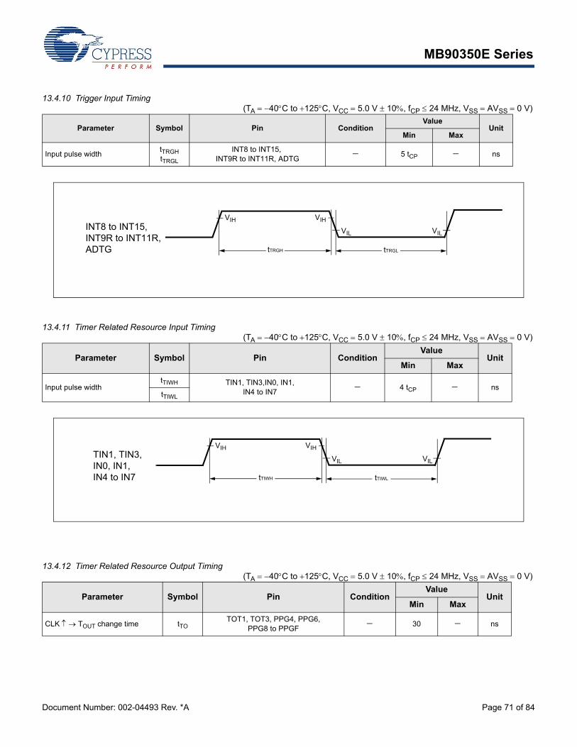
MB90350E Series
Document Number: 002-04493 Rev. *A Page 71 of 84
13.4.10 Trigger Input Timing (TA 40C to 125C, VCC 5.0 V 10, fCP 24 MHz, VSS AVSS 0 V)
13.4.11 Timer Related Resource Input Timing (TA 40C to 125C, VCC 5.0 V 10, fCP 24 MHz, VSS AVSS 0 V)
13.4.12 Timer Related Resource Output Timing (TA 40C to 125C, VCC 5.0 V 10, fCP 24 MHz, VSS AVSS 0 V)
Parameter Symbol Pin ConditionValue
UnitMin Max
Input pulse widthtTRGHtTRGL
INT8 to INT15, INT9R to INT11R, ADTG
5 tCP ns
Parameter Symbol Pin ConditionValue
UnitMin Max
Input pulse widthtTIWH TIN1, TIN3,IN0, IN1,
IN4 to IN7 4 tCP ns
tTIWL
Parameter Symbol Pin ConditionValue
UnitMin Max
CLK TOUT change time tTOTOT1, TOT3, PPG4, PPG6,
PPG8 to PPGF 30 ns
VIL
VIH
tTRGH
VIL
VIH
tTRGL
INT8 to INT15, INT9R to INT11R, ADTG
VIL
VIH
tTIWH
VIL
VIH
tTIWL
TIN1, TIN3,IN0, IN1,IN4 to IN7
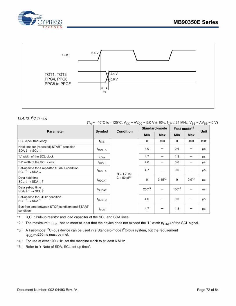
MB90350E Series
Document Number: 002-04493 Rev. *A Page 72 of 84
13.4.13 I2C Timing (TA 40C to 125C, VCC AVCC 5.0 V 10, fCP 24 MHz, VSS AVSS 0 V)
*1 : R,C : Pull-up resistor and load capacitor of the SCL and SDA lines.
*2 : The maximum tHDDAT has to meet at least that the device does not exceed the “L” width (tLOW) of the SCL signal.
*3 : A Fast-mode I2C -bus device can be used in a Standard-mode I2C-bus system, but the requirement tSUDAT250 ns must be met.
*4 : For use at over 100 kHz, set the machine clock to at least 6 MHz.
*5 : Refer to “ Note of SDA, SCL set-up time”.
Parameter Symbol ConditionStandard-mode Fast-mode*4
UnitMin Max Min Max
SCL clock frequency fSCL
R 1.7 k,C 50 pF*1
0 100 0 400 kHz
Hold time for (repeated) START conditionSDA SCL
tHDSTA 4.0 0.6 s
“L” width of the SCL clock tLOW 4.7 1.3 s
“H” width of the SCL clock tHIGH 4.0 0.6 s
Set-up time for a repeated START conditionSCL SDA
tSUSTA 4.7 0.6 s
Data hold timeSCL SDA
tHDDAT 0 3.45*2 0 0.9*3 s
Data set-up timeSDA SCL
tSUDAT 250*5 100*5 ns
Set-up time for STOP conditionSCL SDA
tSUSTO 4.0 0.6 s
Bus free time between STOP condition and START condition
tBUS 4.7 1.3 s
CLK2.4 V
0.8 V
2.4 V
tTO
TOT1, TOT3,PPG4, PPG6PPG8 to PPGF
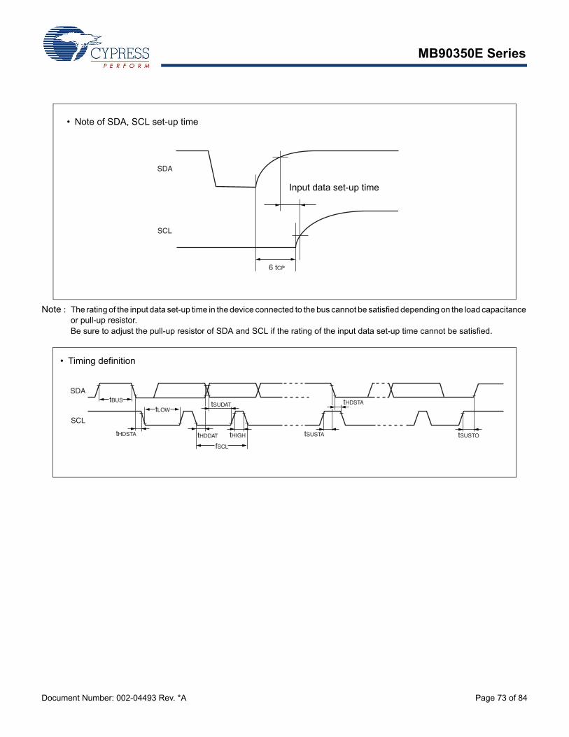
MB90350E Series
Document Number: 002-04493 Rev. *A Page 73 of 84
Note : The rating of the input data set-up time in the device connected to the bus cannot be satisfied depending on the load capacitance or pull-up resistor.Be sure to adjust the pull-up resistor of SDA and SCL if the rating of the input data set-up time cannot be satisfied.
SDA
SCL
6 tCP
• Note of SDA, SCL set-up time
Input data set-up time
SDA
SCL
tBUS
tLOW
fSCL
tHDDAT tHIGH
tSUDAT
tHDSTA tSUSTA
tHDSTA
tSUSTO
• Timing definition
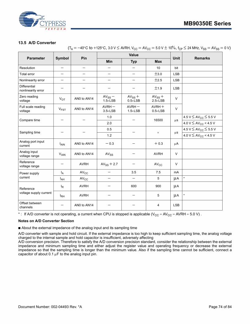
MB90350E Series
Document Number: 002-04493 Rev. *A Page 74 of 84
13.5 A/D Converter (TA 40C to 125C, 3.0 V AVRH, VCC AVCC 5.0 V 10, fCP 24 MHz, VSS AVSS 0 V)
* : If A/D converter is not operating, a current when CPU is stopped is applicable (VCC AVCC AVRH 5.0 V) .
Notes on A/D Converter Section
■ About the external impedance of the analog input and its sampling time
A/D converter with sample and hold circuit. If the external impedance is too high to keep sufficient sampling time, the analog voltagecharged to the internal sample and hold capacitor is insufficient, adversely affecting A/D conversion precision. Therefore to satisfy the A/D conversion precision standard, consider the relationship between the externalimpedance and minimum sampling time and either adjust the register value and operating frequency or decrease the externalimpedance so that the sampling time is longer than the minimum value. Also if the sampling time cannot be sufficient, connect acapacitor of about 0.1 F to the analog input pin.
Parameter Symbol PinValue
Unit RemarksMin Typ Max
Resolution 10 bit
Total error 3.0 LSB
Nonlinearity error 2.5 LSB
Differential nonlinearity error
1.9 LSB
Zero reading voltage
VOT AN0 to AN14AVSS 1.5LSB
AVSS 0.5LSB
AVSS 2.5LSB
V
Full scale reading voltage
VFST AN0 to AN14AVRH 3.5LSB
AVRH 1.5LSB
AVRH 0.5LSB
V
Compare time 1.0
16500 s4.5 V AVCC 5.5 V
2.0 4.0 V AVCC < 4.5 V
Sampling time 0.5
s4.5 V AVCC 5.5 V
1.2 4.0 V AVCC < 4.5 V
Analog port input current
IAIN AN0 to AN14 0.3 0.3 A
Analog input voltage range
VAIN AN0 to AN14 AVSS AVRH V
Reference voltage range
AVRH AVSS 2.7 AVCC V
Power supply current
IA AVCC 3.5 7.5 mA
IAH AVCC 5 A *
Reference voltage supply current
IR AVRH 600 900 A
IRH AVRH 5 A *
Offset between channels
AN0 to AN14 4 LSB
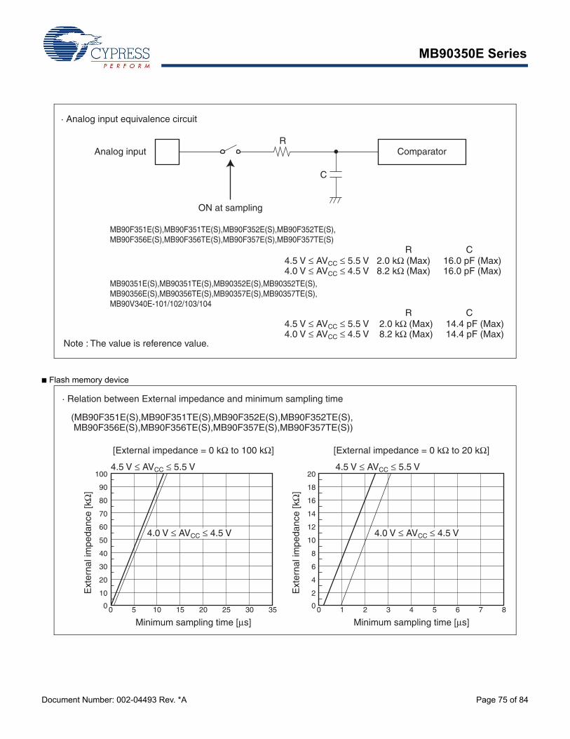
MB90350E Series
Document Number: 002-04493 Rev. *A Page 75 of 84
■ Flash memory device
· Analog input equivalence circuit
ON at sampling
Note : The value is reference value.
R
C
Analog input Comparator
MB90F351E(S),MB90F351TE(S),MB90F352E(S),MB90F352TE(S),MB90F356E(S),MB90F356TE(S),MB90F357E(S),MB90F357TE(S)
CR4.5 V ≤ AVCC ≤ 5.5 V 2.0 kΩ (Max) 16.0 pF (Max)4.0 V ≤ AVCC ≤ 4.5 V 8.2 kΩ (Max) 16.0 pF (Max)
MB90351E(S),MB90351TE(S),MB90352E(S),MB90352TE(S),MB90356E(S),MB90356TE(S),MB90357E(S),MB90357TE(S),MB90V340E-101/102/103/104
CR4.5 V ≤ AVCC ≤ 5.5 V 2.0 kΩ (Max) 14.4 pF (Max)4.0 V ≤ AVCC ≤ 4.5 V 8.2 kΩ (Max) 14.4 pF (Max)
· Relation between External impedance and minimum sampling time
4.5 V ≤ AVCC ≤ 5.5 V
[External impedance = 0 kΩ to 100 kΩ]
Minimum sampling time [μs]
Ext
erna
l im
peda
nce
[kΩ
]
0 5 10 15 20 25 30 35
10
20
30
40
50
60
70
80
90
100
4.0 V ≤ AVCC ≤ 4.5 V
4.5 V ≤ AVCC ≤ 5.5 V
[External impedance = 0 kΩ to 20 kΩ]
Minimum sampling time [μs]
Ext
erna
l im
peda
nce
[kΩ
]
0 1 2 3 4 5 6 7 8
2
4
6
8
10
12
14
16
18
20
4.0 V ≤ AVCC ≤ 4.5 V
(MB90F351E(S),MB90F351TE(S),MB90F352E(S),MB90F352TE(S), MB90F356E(S),MB90F356TE(S),MB90F357E(S),MB90F357TE(S))
0 0
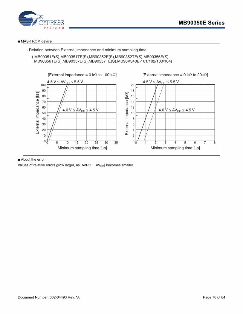
MB90350E Series
Document Number: 002-04493 Rev. *A Page 76 of 84
■ MASK ROM device
■ About the error
Values of relative errors grow larger, as |AVRH AVSS| becomes smaller.
· Relation between External impedance and minimum sampling time
4.5 V ≤ AVCC ≤ 5.5 V
[External impedance = 0 kΩ to 100 kΩ]
Minimum sampling time [μs]
Ext
erna
l im
peda
nce
[kΩ
]
0 5 10 15 20 25 30 35
10
20
30
40
50
60
70
80
90
100
4.0 V ≤ AVCC ≤ 4.5 V
4.5 V ≤ AVCC ≤ 5.5 V
[External impedance = 0 kΩ to 20kΩ]
Minimum sampling time [μs]
Ext
erna
l im
peda
nce
[kΩ
]
0 1 2 3 4 5 6 7 8
2
4
6
8
10
12
14
16
18
20
4.0 V ≤ AVCC ≤ 4.5 V
( MB90351E(S),MB90351TE(S),MB90352E(S),MB90352TE(S),MB90356E(S), MB90356TE(S),MB90357E(S),MB90357TE(S),MB90V340E-101/102/103/104)
0 0
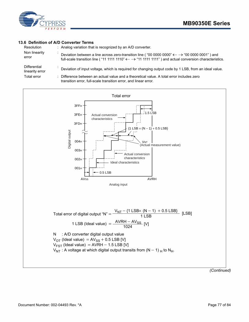
MB90350E Series
Document Number: 002-04493 Rev. *A Page 77 of 84
13.6 Definition of A/D Converter Terms
(Continued)
Resolution : Analog variation that is recognized by an A/D converter.
Non linearity error
: Deviation between a line across zero-transition line ( “00 0000 0000” “00 0000 0001” ) and full-scale transition line ( “11 1111 1110” “11 1111 1111” ) and actual conversion characteristics.
Differential linearity error
: Deviation of input voltage, which is required for changing output code by 1 LSB, from an ideal value.
Total error : Difference between an actual value and a theoretical value. A total error includes zero transition error, full-scale transition error, and linear error.
3FFH
3FEH
3FDH
004H
003H
002H
001H
AVSS AVRH
VNT
1.5 LSB
0.5 LSB
{1 LSB × (N − 1) + 0.5 LSB}
Actual conversioncharacteristics
(Actual measurement value)
Actual conversioncharacteristics
Ideal characteristics
Dig
ital o
utpu
t
Analog input
Total error
Total error of digital output “N” VNT {1 LSB (N 1) 0.5 LSB}
1 LSB[LSB]
1 LSB (Ideal value) AVRH AVSS1024
[V]
N : A/D converter digital output valueVOT (Ideal value) AVSS 0.5 LSB [V]VFST (Ideal value) AVRH 1.5 LSB [V]VNT : A voltage at which digital output transits from (N 1) H to NH.
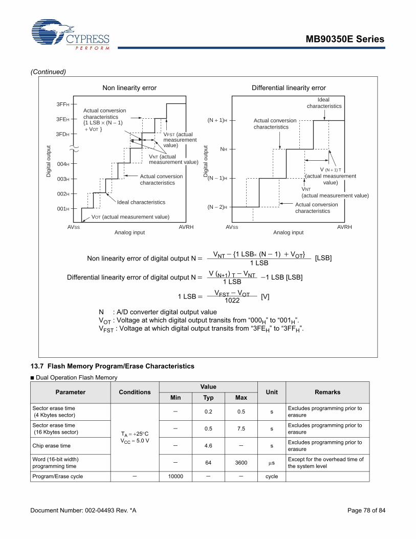
MB90350E Series
Document Number: 002-04493 Rev. *A Page 78 of 84
(Continued)
13.7 Flash Memory Program/Erase Characteristics
■ Dual Operation Flash Memory
Parameter ConditionsValue
Unit RemarksMin Typ Max
Sector erase time (4 Kbytes sector)
TA 25CVCC 5.0 V
0.2 0.5 sExcludes programming prior to erasure
Sector erase time (16 Kbytes sector)
0.5 7.5 sExcludes programming prior to erasure
Chip erase time 4.6 sExcludes programming prior to erasure
Word (16-bit width) programming time
64 3600 sExcept for the overhead time of the system level
Program/Erase cycle 10000 cycle
3FFH
3FEH
3FDH
004H
003H
002H
001H
AVSS AVRH AVSS AVRH
(N + 1)H
NH
(N − 1)H
(N − 2)H
VOT (actual measurement value)
{1 LSB × (N − 1) + VOT }
Actual conversioncharacteristics
VFST (actualmeasurement value)
VNT (actualmeasurement value)
Actual conversioncharacteristics
Ideal characteristics
Actual conversioncharacteristics
Actual conversioncharacteristics
Ideal characteristics
Dig
ital o
utpu
t
Dig
ital o
utpu
t
Analog inputAnalog input
VNT
(actual measurement value)
V (N + 1) T
(actual measurementvalue)
Non linearity error Differential linearity error
Non linearity error of digital output N VNT {1 LSB (N 1) VOT}
1 LSB[LSB]
Differential linearity error of digital output N V (N+1) T VNT
1 LSB1 LSB [LSB]
VFST VOT1022
[V]1 LSB
N : A/D converter digital output valueVOT : Voltage at which digital output transits from “000H” to “001H”.VFST : Voltage at which digital output transits from “3FEH” to “3FFH”.
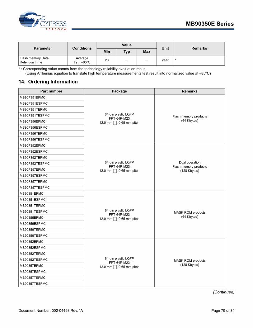
MB90350E Series
Document Number: 002-04493 Rev. *A Page 79 of 84
* : Corresponding value comes from the technology reliability evaluation result. (Using Arrhenius equation to translate high temperature measurements test result into normalized value at 85C)
14. Ordering Information
(Continued)
Flash memory Data Retention Time
AverageTA 85C
20 year *
Part number Package Remarks
MB90F351EPMC
64-pin plastic LQFPFPT-64P-M23
12.0 mm , 0.65 mm pitch
Flash memory products (64 Kbytes)
MB90F351ESPMC
MB90F351TEPMC
MB90F351TESPMC
MB90F356EPMC
MB90F356ESPMC
MB90F356TEPMC
MB90F356TESPMC
MB90F352EPMC
64-pin plastic LQFPFPT-64P-M23
12.0 mm , 0.65 mm pitch
Dual operationFlash memory products
(128 Kbytes)
MB90F352ESPMC
MB90F352TEPMC
MB90F352TESPMC
MB90F357EPMC
MB90F357ESPMC
MB90F357TEPMC
MB90F357TESPMC
MB90351EPMC
64-pin plastic LQFPFPT-64P-M23
12.0 mm , 0.65 mm pitch
MASK ROM products (64 Kbytes)
MB90351ESPMC
MB90351TEPMC
MB90351TESPMC
MB90356EPMC
MB90356ESPMC
MB90356TEPMC
MB90356TESPMC
MB90352EPMC
64-pin plastic LQFPFPT-64P-M23
12.0 mm , 0.65 mm pitch
MASK ROM products (128 Kbytes)
MB90352ESPMC
MB90352TEPMC
MB90352TESPMC
MB90357EPMC
MB90357ESPMC
MB90357TEPMC
MB90357TESPMC
Parameter ConditionsValue
Unit RemarksMin Typ Max
MB90350E Series
Document Number: 002-04493 Rev. *A Page 80 of 84
(Continued)Part number Package Remarks
MB90F351EPMC1
64-pin plastic LQFPFPT-64P-M24
10.0 mm , 0.50 mm pitch
Flash memory products (64 Kbytes)
MB90F351ESPMC1
MB90F351TEPMC1
MB90F351TESPMC1
MB90F356EPMC1
MB90F356ESPMC1
MB90F356TEPMC1
MB90F356TESPMC1
MB90F352EPMC1
64-pin plastic LQFPFPT-64P-M24
10.0 mm , 0.50 mm pitch
Dual operationFlash memory products
(128 Kbytes)
MB90F352ESPMC1
MB90F352TEPMC1
MB90F352TESPMC1
MB90F357EPMC1
MB90F357ESPMC1
MB90F357TEPMC1
MB90F357TESPMC1
MB90351EPMC1
64-pin plastic LQFPFPT-64P-M24
10.0 mm , 0.50 mm pitch
MASK ROM products (64 Kbytes)
MB90351ESPMC1
MB90351TEPMC1
MB90351TESPMC1
MB90356EPMC1
MB90356ESPMC1
MB90356TEPMC1
MB90356TESPMC1
MB90352EPMC1
64-pin plastic LQFPFPT-64P-M24
10.0 mm , 0.50 mm pitch
MASK ROM products (128 Kbytes)
MB90352ESPMC1
MB90352TEPMC1
MB90352TESPMC1
MB90357EPMC1
MB90357ESPMC1
MB90357TEPMC1
MB90357TESPMC1
MB90V340E-101CR
299-pin ceramic PGAPGA-299C-A01
Device for evaluationMB90V340E-102CR
MB90V340E-103CR
MB90V340E-104CR
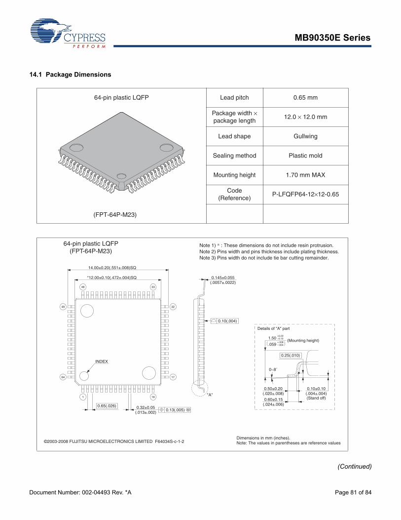
MB90350E Series
Document Number: 002-04493 Rev. *A Page 81 of 84
14.1 Package Dimensions
(Continued)
64-pin plastic LQFP Lead pitch 0.65 mm
Package width ×package length
12.0 × 12.0 mm
Lead shape Gullwing
Sealing method Plastic mold
Mounting height 1.70 mm MAX
Code(Reference)
P-LFQFP64-12×12-0.65
64-pin plastic LQFP(FPT-64P-M23)
(FPT-64P-M23)
C 2003 FUJITSU LIMITED F64034S-c-1-1
0.65(.026)
0.10(.004)
1 16
17
3249
64
3348
*12.00±0.10(.472±.004)SQ
14.00±0.20(.551±.008)SQ
INDEX
0.32±0.05(.013±.002)
M0.13(.005)
0.145±0.055(.0057±.0022)
"A"
.059 –.004+.008
–0.10+0.20
1.50
0~8˚
0.25(.010)
(Mounting height)
0.50±0.20(.020±.008)0.60±0.15
(.024±.006)
0.10±0.10(.004±.004)
Details of "A" part
(Stand off)
Dimensions in mm (inches).Note: The values in parentheses are reference values©2003-2008 FUJITSU MICROELECTRONICS LIMITED F64034S-c-1-2
Note 1) * : These dimensions do not include resin protrusion.Note 2) Pins width and pins thickness include plating thickness.Note 3) Pins width do not include tie bar cutting remainder.
MB90350E Series
Document Number: 002-04493 Rev. *A Page 82 of 84
(Continued)
64-pin plastic LQFP Lead pitch 0.50 mm
Package width ×package length
10.0 × 10.0 mm
Lead shape Gullwing
Sealing method Plastic mold
Mounting height 1.70 mm MAX
Weight 0.32 g
Code(Reference)
P-LFQFP64-10×10-0.50
64-pin plastic LQFP(FPT-64P-M24)
(FPT-64P-M24)
LEAD No.
Details of "A" part
0.25(.010)
(Stand off)(.004±.004)0.10±0.10
(.024±.006)0.60±0.15
(.020±.008)0.50±0.20
1.50+0.20–0.10
+.008–.004.059
0˚~8˚
"A"
0.08(.003)
(.006±.002)0.145±0.055
0.08(.003) M(.008±.002)0.20±0.050.50(.020)
12.00±0.20(.472±.008)SQ
10.00±0.10(.394±.004)SQ
INDEX
49
64
3348
17
32
161
2005 FUJITSU LIMITED F64036S-c-1-1C
(Mounting height)
*
Dimensions in mm (inches).Note: The values in parentheses are reference values©2005-2008 FUJITSU MICROELECTRONICS LIMITED F64036S-c-1-2
Note 1) * : These dimensions do not include resin protrusion.Note 2) Pins width and pins thickness include plating thickness.Note 3) Pins width do not include tie bar cutting remainder.
MB90350E Series
Document Number: 002-04493 Rev. *A Page 83 of 84
15. Major Changes
NOTE: Please see “Document History” about later revised information.
Document History
Page Section Change Results
The following names are changed.UART LIN-UART16-bit I/O timer 16-bit free-run timer
26 Handling Devices Added the section ”13. Serial Communication”.
51 Electrical CharacteristicsAbsolute Maximum Ratings
Changed the maximum value of power consumption.
63 Electrical CharacteristicsAC Characteristics
Changed the "(4) Clock Output Timing".Changed the Minimum value of cycle time.(41.76 41.67)
69 to 73 Changed the notation of “(9) LIN-UART”.
78 A/D Converter Changed the notation of “Zero reading voltage” and “full scale reading voltage”.
85 Ordering Information Changed the part number;MB90V340E-101 MB90V340E-101CRMB90V340E-102 MB90V340E-102CRMB90V340E-103 MB90V340E-103CRMB90V340E-104 MB90V340E-104CR
Document Title: MB90350E Series F2MC-16LX 16-bit Microcontrollers Document Number: 002-04493
Revision ECN Orig. of Change
Submission Date Description of Change
** AKIH 10/12/2006 Migrated to Cypress and assigned document number 002-04993.No change to document contents or format.
*A 5193077 AKIH 04/07/2016 Updated to Cypress template
Document Number: 002-04493 Rev. *A Revised April 7, 2016 Page 84 of 84
MB90350E Series
© Cypress Semiconductor Corporation, 2006-2016. This document is the property of Cypress Semiconductor Corporation and its subsidiaries, including Spansion LLC (“Cypress”). This document, including any software or firmware included or referenced in this document (“Software”), is owned by Cypress under the intellectual property laws and treaties of the United States and other countries worldwide. Cypress reserves all rights under such laws and treaties and does not, except as specifically stated in this paragraph, grant any license under its patents, copyrights, trademarks, or other intellectual property rights. If the Software is not accompanied by a license agreement and you do not otherwise have a written agreement with Cypress governing the use of the Software, then Cypress hereby grants you a personal, non-exclusive, nontransferable license (without the right to sublicense) (1) under its copyright rights in the Software (a) for Software provided in source code form, to modify and reproduce the Software solely for use with Cypress hardware products, only internally within your organization, and (b) to distribute the Software in binary code form externally to end users (either directly or indirectly through resellers and distributors), solely for use on Cypress hardware product units, and (2) under those claims of Cypress’s patents that are infringed by the Software (as provided by Cypress, unmodified) to make, use, distribute, and import the Software solely for use with Cypress hardware products. Any other use, reproduction, modification, translation, or compilation of the Software is prohibited.
TO THE EXTENT PERMITTED BY APPLICABLE LAW, CYPRESS MAKES NO WARRANTY OF ANY KIND, EXPRESS OR IMPLIED, WITH REGARD TO THIS DOCUMENT OR ANY SOFTWARE OR ACCOMPANYING HARDWARE, INCLUDING, BUT NOT LIMITED TO, THE IMPLIED WARRANTIES OF MERCHANTABILITY AND FITNESS FOR A PARTICULAR PURPOSE. To the extent permitted by applicable law, Cypress reserves the right to make changes to this document without further notice. Cypress does not assume any liability arising out of the application or use of any product or circuit described in this document. Any information provided in this document, including any sample design information or programming code, is provided only for reference purposes. It is the responsibility of the user of this document to properly design, program, and test the functionality and safety of any application made of this information and any resulting product. Cypress products are not designed, intended, or authorized for use as critical components in systems designed or intended for the operation of weapons, weapons systems, nuclear installations, life-support devices or systems, other medical devices or systems (including resuscitation equipment and surgical implants), pollution control or hazardous substances management, or other uses where the failure of the device or system could cause personal injury, death, or property damage (“Unintended Uses”). A critical component is any component of a device or system whose failure to perform can be reasonably expected to cause the failure of the device or system, or to affect its safety or effectiveness. Cypress is not liable, in whole or in part, and you shall and hereby do release Cypress from any claim, damage, or other liability arising from or related to all Unintended Uses of Cypress products. You shall indemnify and hold Cypress harmless from and against all claims, costs, damages, and other liabilities, including claims for personal injury or death, arising from or related to any Unintended Uses of Cypress products.
Cypress, the Cypress logo, Spansion, the Spansion logo, and combinations thereof, PSoC, CapSense, EZ-USB, F-RAM, and Traveo are trademarks or registered trademarks of Cypress in the UnitedStates and other countries. For a more complete list of Cypress trademarks, visit cypress.com. Other names and brands may be claimed as property of their respective owners.
Sales, Solutions, and Legal Information
Worldwide Sales and Design Support
Cypress maintains a worldwide network of offices, solution centers, manufacturer’s representatives, and distributors. To find the office closest to you, visit us at Cypress Locations.
Products
ARM® Cortex® Microcontrollers cypress.com/arm
Automotive cypress.com/automotive
Clocks & Buffers cypress.com/clocks
Interface cypress.com/interface
Lighting & Power Control cypress.com/powerpsoc
Memory cypress.com/memory
PSoC cypress.com/psoc
Touch Sensing cypress.com/touch
USB Controllers cypress.com/usb
Wireless/RF cypress.com/wireless
PSoC® Solutions
cypress.com/psoc
PSoC 1 | PSoC 3 | PSoC 4 | PSoC 5LP
Cypress Developer Community
Community | Forums | Blogs | Video | Training
Technical Support
cypress.com/support


