Embed Size (px)
Citation preview
Phase Separation and Magnetic Order in K-doped Iron Selenide
Superconductor
Wei Li1, Hao Ding1, Peng Deng1, Kai Chang1, Canli Song1, Ke He2, Lili Wang2, Xucun Ma2,
Jiang-Ping Hu3, Xi Chen1, *, and Qi-Kun Xue1, *
* To whom correspondence should be addressed. Email: [email protected],
The newly discovered alkali-doped iron selenide superconductors1,2 not only
reach a superconducting transition temperature as high as 32 K, but also exhibit
several unique characters that are noticeably absent in other iron-based
superconductors, such as antiferromagnetically ordered insulating phases3,4, extremely
high Neel transition temperatures5,6, and the presence of intrinsic Fe vacancies and
ordering7-9. These features have generated considerable excitements as well as
confusions, regarding the delicate interplay between Fe vacancies, magnetism and
superconductivity10-12, on which there is no consensus to date. Here we report on
molecular beam epitaxy (MBE) growth of high-quality KxFe2-ySe2 thin films and in
situ low-temperature scanning tunneling microscope (STM) measurement of their
atomic and electronic structures. We unambiguously demonstrate that a KxFe2-ySe2
sample contains two distinct phases: an insulating phase with well-defined 5 5
order of Fe vacancies, and a superconducting KFe2Se2 phase containing no Fe
vacancies. We further show that the vacancy and magnetism are strongly coupled and
an individual Fe vacancy can locally destroy superconductivity in a similar way as a
magnetic impurity in conventional superconductors. The measurement of magnetic
field dependence of the Fe-vacancy-induced bound states explicitly reveals a hidden
magnetically-related bipartite order in the tetragonal iron lattice. These findings
elucidate the existing controversies on this new superconductor and provide atomistic
information on understanding the interplay between magnetism and superconductivity
in iron-based superconductors.
Our experiments were conducted in a Unisoku ultra-high vacuum (UHV) low
temperature (down to 0.4 K) STM equipped with an MBE chamber for thin film
growth. Magnetic field up to 11 T can be applied perpendicular to the sample surface.
We grew KxFe2-ySe2 thin films on the graphitized 6H-SiC(0001) substrate. High
purity Fe (99.995%), Se (99.9999%) and K were evaporated from two standard

Knudsen cells and one SAES getter, respectively. The growth was carried out under
Se-rich condition with a nominal Se/Fe flux ratio of ~20, which is known to lead to
stoichiometric and superconductive FeSe13. To intercalate K atoms in between FeSe
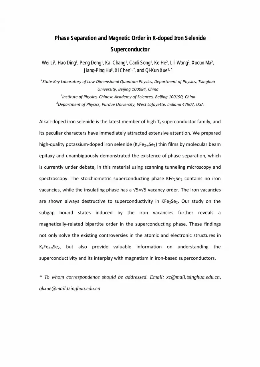
layers (see the schematic crystal structure of KFe2Se2 in Fig. 1A), the substrate was
held at 440°C during growth and the sample was subsequently annealed at 470°C for
three hours. The K flux is relatively flexible, which determines the area ratio of two
different phases as shown below. The STM image in Fig. 1B shows the typical
atomically flat surface of a sample.
Two distinct regions (marked by I and II in Fig. 1B), coexisting side by side, are
clearly revealed in the film, indicating that phase separation7, 12 occurs. The STM
image with atomic resolution (Fig. 1C) of region I exhibits a centered rectangular
lattice structure. The periods along the two orthogonal directions are 5.5 Å and 14.1 Å,
respectively, as shown in Fig. 1C. Comparison with X-ray diffraction data suggests
that the orientation of the film is (110) (see Fig. 1D) instead of the natural cleavage
plane (001). Thus the STM actually images the cross-section of the layered material.
The (110) plane is terminated with K and Se atoms. The K atoms are visible at
positive bias and form atomic rows (Fig. 1C), which are 7.05 Å apart and oriented
along the [ 110 ] direction. At negative bias, the Se atomic rows (indicated by black
dots in Fig. 1E) appear and zigzag through the K atoms. These images are fully
consistent with the atomic structure of the (110) surface (Fig. 1D). Furthermore, our
STM observation shows that there are very few defects in region I. We therefore
identify region I as the stoichiometric KFe2Se2.
The scanning tunneling spectroscopy (STS) probes the quasiparticle density of
states (DOS). In Fig. 1F, we show the STS at 0.4 K in region I. The spectrum exhibits
a superconducting gap centered at the Fermi energy and two characteristic coherence
peaks, indicating that the stoichiometric phase KFe2Se2 is a superconductor. As
expected, the gap and coherence peaks gradually disappear at higher temperatures as
shown in the temperature-dependent tunneling spectra (fig. S1). Similar to cuprate14
and iron-pnictide15,16 superconductors, the electron-hole asymmetry is clearly
noticeable in STS.
The STS reveals a double-gap structure. The larger gap 1=4 meV is half of the
energy between the two pronounced coherence peaks. The smaller one, roughly 2~1
meV, is estimated by the two shoulders near the Fermi energy in the spectra. The
coherence peaks of the smaller gap are hardly distinguishable because of thermal
broadening. Nearly isotropic gaps have also been observed by angle-resolved
photoemission spectroscopy (ARPES) 17-20 on the electron-like Fermi surfaces near M
and points, giving rise to 1, whereas 2 is too small to be resolved by ARPES.
The finite-size effect on superconductivity is negligible because the typical size
of region I, 20 nm thick (along the [110] direction in a-b plane) and 50 nm wide
(along the c and [ 110 ] directions), is much larger than the superconducting coherence
length of KFe2Se2. Here the anisotropic coherence lengths ab~2 nm and c~0.5 nm
can be estimated by the upper critical fields21,22 in the a-b plane and along the c
direction using Hc2ab= 0/2 ab c and Hc2
c= 0/2 ab2, respectively. On the other hand,
the penetration depth23 of the material is much larger than the sample size. Under this
circumstance, the magnetic field is essentially uniform in a sample. Different from our
previous work on FeSe13, no vortex core has been resolved in the zero-bias
conductance map of KFe2Se2 probably due to the large penetration depth. However,
the effect of magnetic field on superconductivity in KFe2Se2 is still clearly manifested
in STS. Magnetic field breaks time-reversal symmetry and weakens superconductivity,
giving rise to a reduction in the height of coherence peak in DOS (see fig. S2).
Because of the good sample quality, the superconducting gap exhibits high spatial
homogeneity, as shown in Figs. 1G and 1H. Previous studies of iron-based
superconductors usually suffer from various imperfections in the materials24. It is
therefore very crucial to prepare high-quality samples. As mentioned above, we
solved this problem by MBE growth under well-controlled conditions (see also Ref.
13). In addition, surface contamination is avoided since our film growth and STM
study were conducted in a single UHV system. More significantly, by growing films
with (110)-oriented crystallographic surface where both K and Se atoms are exposed,
we have realized the cross-sectional tunneling configuration. Such configuration for
unconventional superconductors has been highly desirable, but very challenging to
achieve due to the difficulty in preparing a suitable surface for STM studies25.
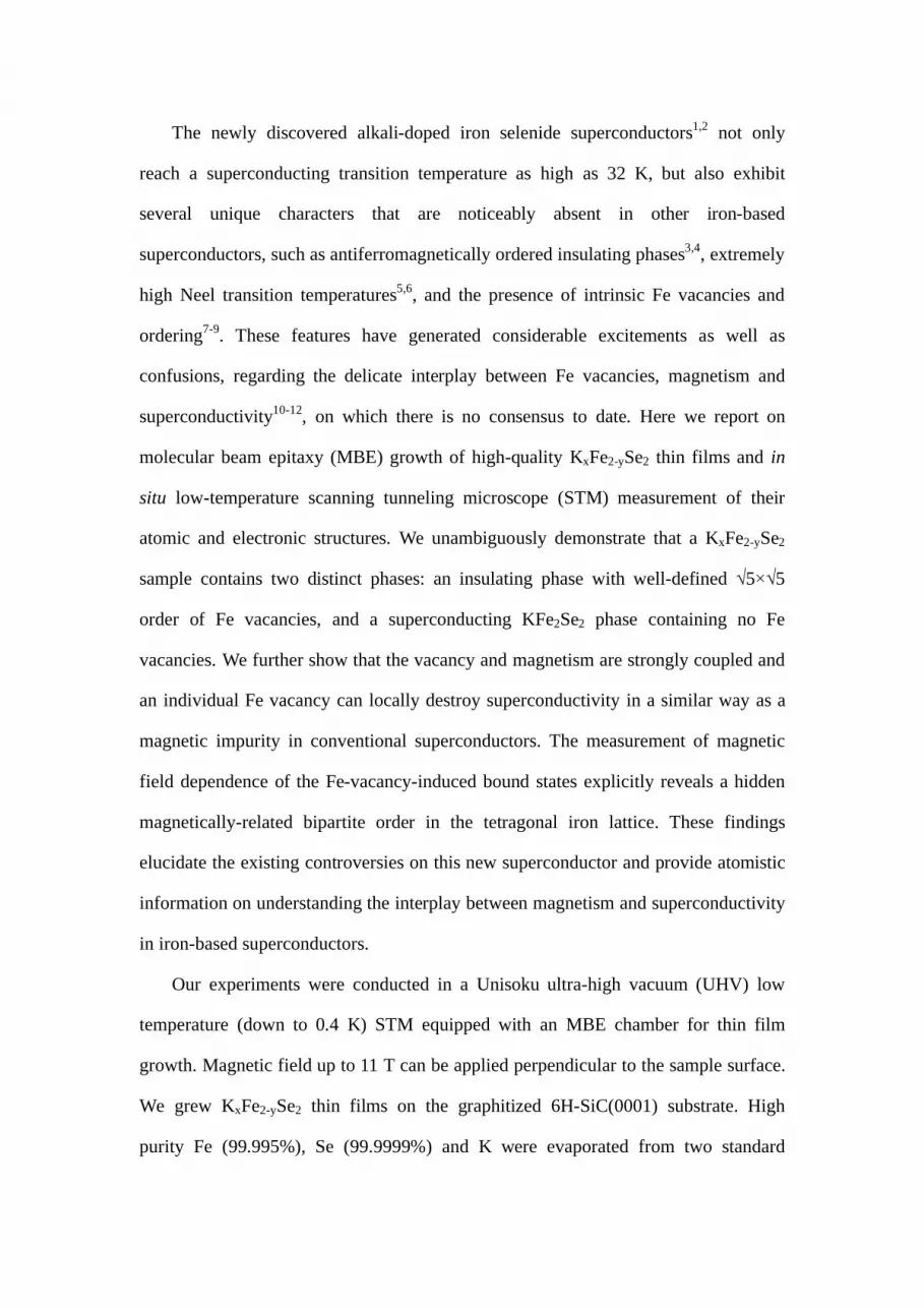
Now we turn to region II, which shows periodic stripe pattern (Fig. 1B). The STS
in Fig. 2A exhibits an energy gap up to 0.43 eV across the Fermi level, suggesting that
this region is insulating. Besides the K atomic rows in the topmost layer, there is a
superposed striped structure with a period of 14.0 Å in the STM image (Fig. 2B). The
stripes are along the c-axis and perpendicular to the K atomic rows. We attribute this
superstructure to the 5 5 pattern of Fe vacancies in the second atomic layer. They
are visible in STM images because the electronic structure of the topmost layer is
perturbed by the missing Fe-Se bonds. Neutron scattering5, transmission electron
microscopy7 and X-ray diffraction8 measurements have all revealed a 5 5 order
formed by Fe vacancies. Such a blocked checkerboard pattern9 gives rise to a
5aFe~14.0 Å periodicity in the (110) plane (Fig. 2C) and is consistent with the
superstructure observed in our STM images. Here aFe is the in-plane distance between
two neighboring Fe atoms. The 5 5 vacancy order leads to a composition of
KxFe1.6Se2, where x is either 1 or 0.8. As illustrated in fig. S3, among every five
consecutive bright spots along the K atomic row, the one in the middle appears
different from the other four. The STM image alone cannot tell if this difference is
due to the missing of one K atom (x=0.8) or simply electronic feature (x=1), thus
leaving the value of x undetermined.
The above STM study, which combines the capabilities of imaging and
spectroscopy together, has thus explicitly proved that KxFe2-ySe2 is composed of two
different phases, i.e., superconducting KFe2Se2 and insulating KxFe1.6Se2. The 5 5
ordered pattern of Fe vacancies only exists in the insulating phase. As discussed
below, our further experiment demonstrates that the superconducting phase has a
hidden order related to Fe as well.
Defect-induced subgap states in superconductors, which can be detected by local
probes such as STM/STS26-28, have often been used to uncover the nature of
superconducting state and magnetic interaction. To reveal the hidden order, we
introduced defects (bright parallelograms in Fig. 3A) into the superconducting
KFe2Se2 phase by annealing the sample at 450°C for several hours. The atomically
resolved STM images indicate that the topmost layer remains perfect lattice without K
or Se vacancies (fig. S4). The resulted defects are always located in the middle
between two adjacent K atomic rows. We therefore attribute the parallelogram-shaped
structures to single Fe vacancies in the second atomic layer (Fig. 3B). By examining
the registration of Fe sites with respect to the Se lattice in the topmost layer, the Fe
atoms in the (110) plane can be divided into two interpenetrating sublattices. The Fe
vacancies on two different sublattices are labeled by A and B, respectively. The
atomic structure, chemical environment and STM images of these two types of
vacancies are mirror-images of each other.
A Fe vacancy carries spin and breaks superconducting pairing in the singlet
channel through spin-flip scattering. The exchange interaction JS·Svac, where S and
Svac are the spins of a quasiparticle and a vacancy, respectively, gives rise to the
bound quasiparticle states. The STS on a vacancy (Fig. 3C) shows strongly
suppressed coherence peaks and a pair of resonances inside the superconducting gap,
i.e., an electron-like bound state at 1.9 mV and a hole-like bound state at -1.9 mV.
While the energies of the electron-like and hole-like states are symmetric with respect
to zero bias, their amplitudes are different as a result of on-site Coulomb interaction29.
The spatial extent of a resonance peak as shown in the dI/dV mapping (Fig. 3D) is
comparable with the coherence lengths in [ 110 ] and [001] directions. A vacancy is
considered to be isolated if no others exist within twice the coherence length. The
spectra on all isolated vacancies are identical, indicating that type-A and B vacancies
have the same magnitude of magnetic moment and the same exchange interaction J.
The spectrum itself does not provide direct information on the orientation of magnetic
moment.
To reveal the spin orientations of the two types (A and B) of vacancies, we apply
a magnetic field perpendicular to the sample surface to break the rotational symmetry.
To date, the magnetic field effect on defect-induced subgap resonance has not been
observed. However, in KFe2Se2, the observation of such effect becomes possible
owing to the high upper critical field and large penetration depth. As clearly shown in
Figs. 3E and 3F, the energy of the subgap resonance in KFe2Se2 exhibits a linear
dependence on magnetic field B: E=E0+gμBB S, where μB is the Bohr magneton and g
the Landé factor. Fitting the data to a line (Fig. 3G) gives g=2.07 0.07, close to
2.0023 of a free electron. The most striking behavior of the field effect is that the
peaks on type-A and B vacancies shift to opposite directions with magnetic field. The
opposite shifting suggests that the two types of vacancies have different spin
orientations, implying a magnetically-related bipartite order in the tetragonal Fe lattice.
Such bipartite structure may account for the large electron-like Fermi surface sheet
with weak intensity near point in ARPES data19,20 through Brillouin zone folding.
The interplay between magnetism and superconductivity is one of the most
intriguing phenomena in high Tc superconductors. The technique mentioned above
can sensitively probe local magnetism in superconductors and may help to understand
how superconductivity arises in high Tc materials.
We have demonstrated that a single Fe vacancy locally suppresses Cooper pairing.
The role of Fe vacancies in the superconducting phase has been rather controversial in
previous studies. For example, some experiment suggested that randomly distributed
vacancies may help to stabilize the superconducting state12. To further elucidate the
effect of Fe vacancies on superconductivity, we prepared samples with higher density
of randomly distributed vacancies (see Fig. 4A) by UHV annealing. The STS in Fig.
4B shows that a sample with high density of vacancies eventually becomes a gapless
superconductor. Therefore the Fe vacancies are always destructive to
superconductivity in KFe2Se2.
References and Notes
1. J. Guo et al., Phys. Rev. B 82, 180520(R) (2010).
2. A. F. Wang et al., Phys. Rev. B 83, 060512(R) (2011).
3. M.-H. Fang et al., Europhys. Lett. 94, 27009 (2011).
4. Z. G. Chen et al., Phys. Rev. B 83, 220507(R) (2011).
5. W. Bao et al., http://arxiv.org/abs/1102.0830 (2011).
6. V. Yu. Pomjakushin et al., Phys. Rev. B 83, 144410 (2011).
7. Z. Wang et al., Phys. Rev. B 83, 140505(R) (2011).
8. P. Zavalij et al., Phys. Rev. B 83, 132509 (2011).
9. X.-W. Yan, M. Gao, Z.-Y. Lu, T. Xiang, Phys. Rev. B 83, 233205 (2011).
10. Z. Shermadini et al., Phys. Rev. Lett. 106, 117602 (2011).
11. W. Bao et al., http://arxiv.org/abs/1102.3674 (2011).
12. B. Shen et al., http://arxiv.org/abs/1104.2008 (2011).
13. C.-L. Song et al., Science 332, 1410 (2011).
14. Y. Kohsaka et al., Science 315, 1380 (2007).
15. M. C. Boyer et al., http://arxiv.org/abs/0806.4400 (2008).
16. F. C. Niestemski et al., http://arxiv.org/abs/0906.2761 (2009).
17. Y. Zhang et al., Nat. Mater. 10, 273 (2011).
18. T. Qian et al., Phys. Rev. Lett. 106, 187001 (2011).
19. L. Zhao et al., Phys. Rev. B 83, 140508(R) (2011).
20. X.-P. Wang et al., Europhys. Lett. 93, 57001 (2011).
21. Z. Gao et al., http://arxiv.org/abs/1103.2904 (2011).
22. E. D. Mun et al., Phys. Rev. B 83, 100514(R) (2011).
23. D. A. Torchetti et al., Phys. Rev. B 83, 104508 (2011).
24. D. C. Johnston, Adv. Phys. 59, 803 (2010).
25. Ø. Fischer et al., Rev. Mod. Phys. 79, 353 (2007) and references therein.
26. A. Yazdani et al., Science 275, 1767 (1997).

27. S.-H. Ji et al., Phys. Rev. Lett. 100, 226801 (2008).
28. A. V. Balatsky, I. Vekhter, J.-X. Zhu, Rev. Mod. Phys. 78, 373 (2006).
29. M. I. Salkola, A. V. Balatsky, J. R. Schrieffer, Phys. Rev. B 55, 12648 (1997).
Acknowledgements: We thank Y. G. Zhao for helpful discussions. The work was financially
supported by National Science Foundation and Ministry of Science and Technology of China.

Figure Captions
Fig. 1. MBE film and the superconducting phase of KxFe2-ySe2. (A) The crystal
structure of KFe2Se2. The same conventions for atoms and Miller indices are used
throughout. (B) STM topographic image (bias voltage V=3.9 V, tunneling current
It=0.02 nA) of a KxFe2-ySe2 film. The grain size is usually larger than 50 nm 50 nm.
Two distinct regions are labeled by I and II, respectively. (C) Atomic-resolution STM
topography of region I (5 nm 5 nm, V=0.15 V, It=0.03 nA). The K atoms are visible
at positive bias. (D) Atomic structure of (110) plane. K and Se atoms are in the
topmost layer. Fe atoms are in the second layer. (E) STM image of the same area as
(C), but at negative bias. V=-2 V, It=-0.03 nA. Se atoms (marked by black dots) are
visible. The positions of K atoms are marked by white dots. (F) Differential
conductance spectrum in region I measured at 0.4 K (setpoint: V=14 mV, It=0.1 nA).
(G-H) Uniformity of the superconducting gap. The spectra in (H) were measured
along the white line in (G). The size of image in (G) is 20 nm 20 nm. The setpoint:
V=14 mV, It=0.1 nA.
Fig. 2. The insulating phase. (A) Differential conductance spectrum in region II
(setpoint: V=1.1 V, It=0.26 nA). (B) Atomic-resolution STM topography of region II
(10 nm 10 nm, V=2.9 V, It=0.02 nA). (C) The structure of 5 5 Fe vacancy
pattern as seen from (001) and (110) planes, respectively. The positions of Fe
vacancies are marked by crosses.
Fig. 3. Fe vacancy-induced bound states in the superconducting gap of KFe2Se2. (A, B)
STM topography (12 nm 12 nm, V=30 mV, It=0.03 nA) and atomic structure of Fe
vacancies. Two types of vacancies are labeled by A and B, respectively. (C, D) dI/dV
spectrum measured at 0.4 K (setpoint, V=15 mV, It=0.1 nA) and density of states map
of the bound state on a single Fe vacancy (4 nm 4 nm, 2 mV). The tunneling
junction was set by 25 mV and 0.16 nA during mapping. The positions of Fe vacancy,
K atoms and Se atoms are marked a cross, black dots and white dots, respectively. (E
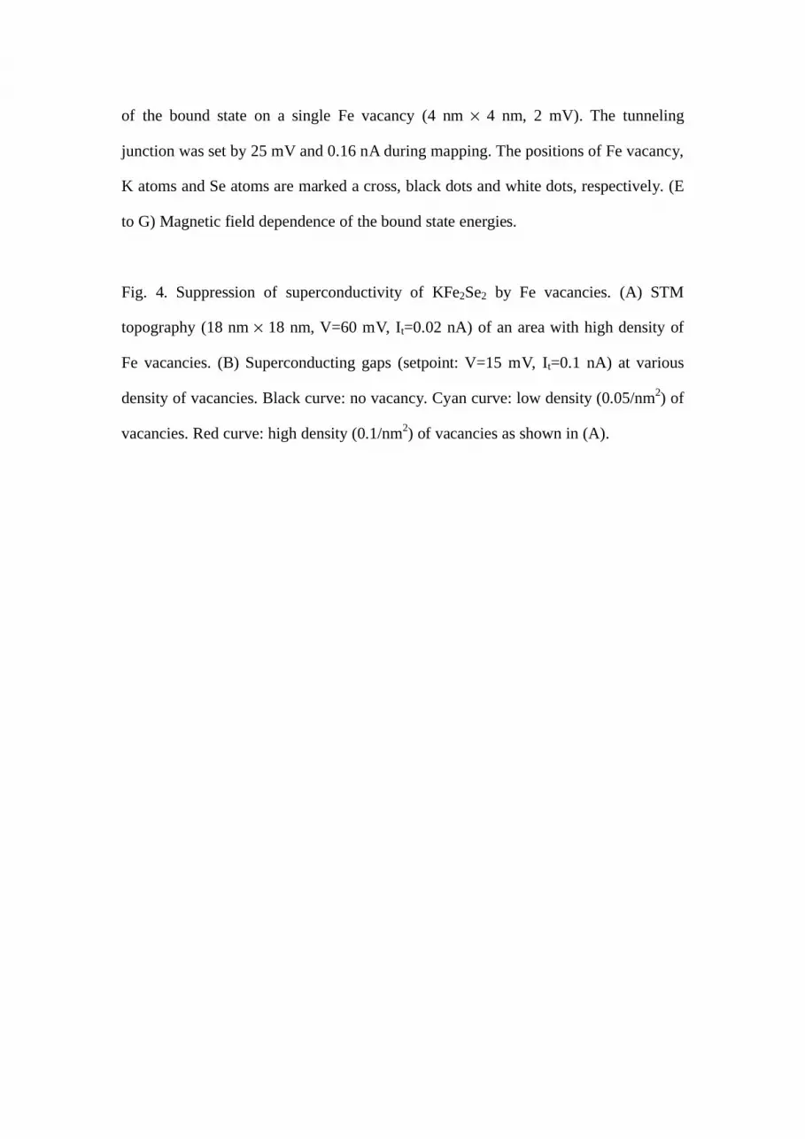
to G) Magnetic field dependence of the bound state energies.
Fig. 4. Suppression of superconductivity of KFe2Se2 by Fe vacancies. (A) STM
topography (18 nm 18 nm, V=60 mV, It=0.02 nA) of an area with high density of
Fe vacancies. (B) Superconducting gaps (setpoint: V=15 mV, It=0.1 nA) at various
density of vacancies. Black curve: no vacancy. Cyan curve: low density (0.05/nm2) of
vacancies. Red curve: high density (0.1/nm2) of vacancies as shown in (A).

Figure 1

Figure 2

Figure 3
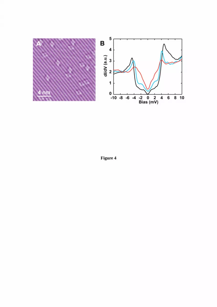
Figure 4
Supporting Materials for
Phase Separation and Magnetic Order in K-doped Iron Selenide
Superconductor
Wei Li1, Hao Ding1, Peng Deng1, Kai Chang1, Canli Song1, Ke He2, Lili Wang2, Xucun Ma2, Jiang-Ping Hu3,
Xi Chen1, *, and Qi-Kun Xue1, *
* To whom correspondence should be addressed. Email: [email protected],

Fig. S1. Temperature dependence of differential tunneling conductance of the superconducting
phase KFe2Se2. Setpoint: V=25 mV, It=0.16 nA. The curves are offset vertically for clarity.
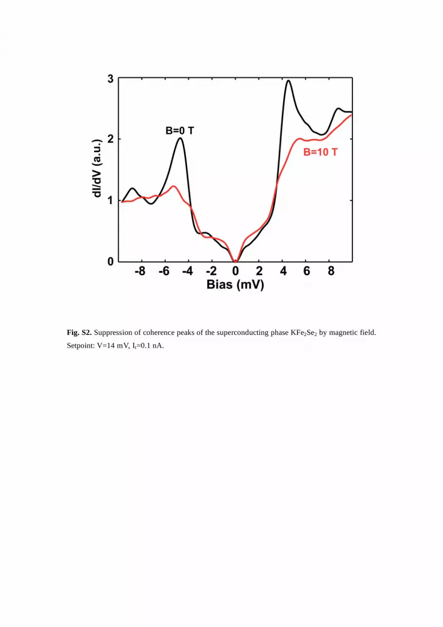
Fig. S2. Suppression of coherence peaks of the superconducting phase KFe2Se2 by magnetic field.
Setpoint: V=14 mV, It=0.1 nA.
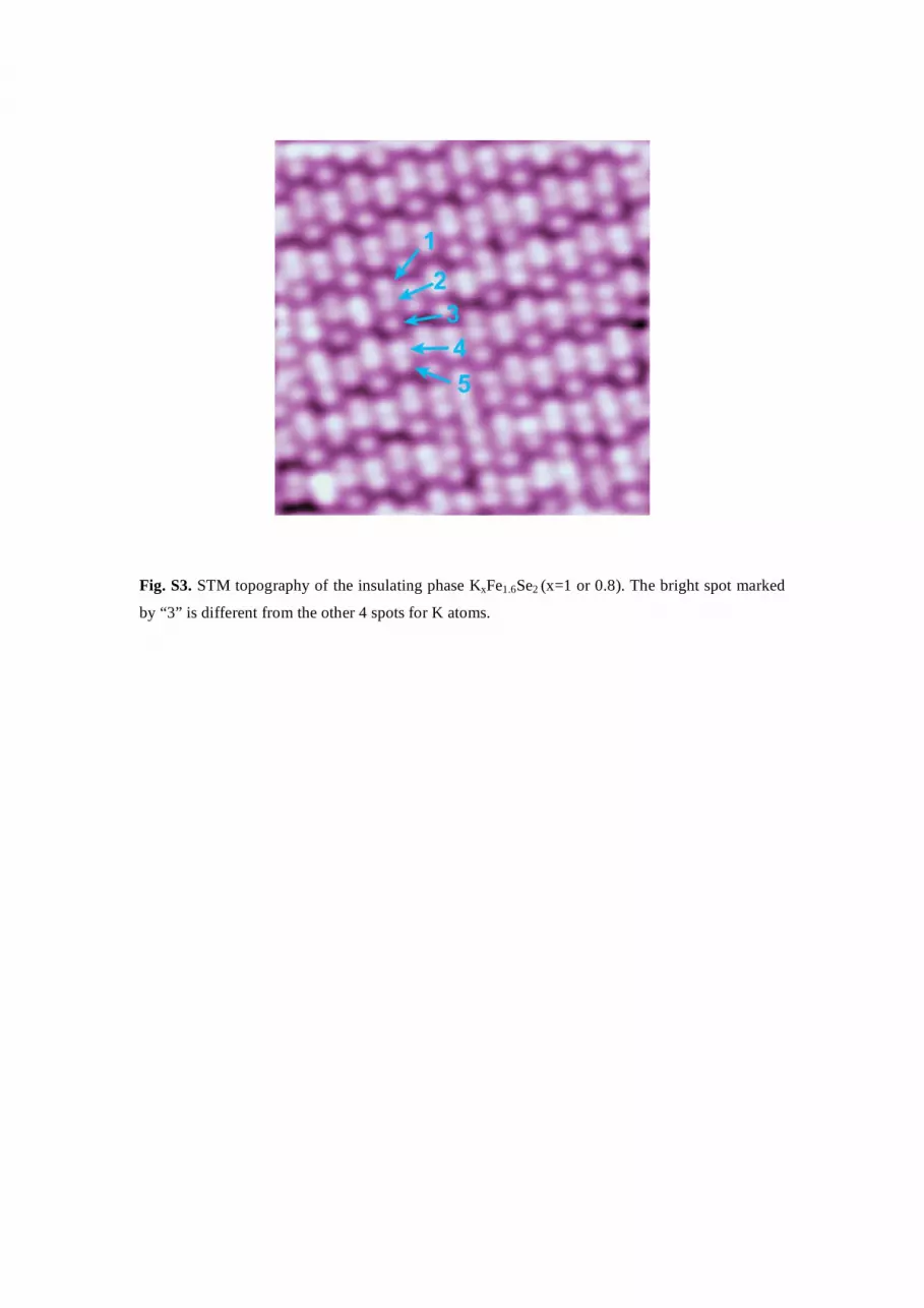
Fig. S3. STM topography of the insulating phase KxFe1.6Se2 (x=1 or 0.8). The bright spot marked
by “3” is different from the other 4 spots for K atoms.
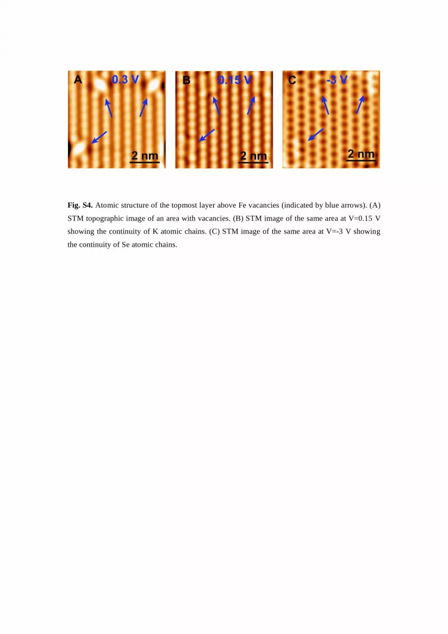
Fig. S4. Atomic structure of the topmost layer above Fe vacancies (indicated by blue arrows). (A)
STM topographic image of an area with vacancies. (B) STM image of the same area at V=0.15 V
showing the continuity of K atomic chains. (C) STM image of the same area at V=-3 V showing
the continuity of Se atomic chains.


