Embed Size (px)
Citation preview

Seediscussions,stats,andauthorprofilesforthispublicationat:https://www.researchgate.net/publication/221031516
Packagelevelinterconnectoptions
CONFERENCEPAPER·JANUARY2005
DOI:10.1145/1053355.1053361·Source:DBLP
CITATIONS
12
READS
11
7AUTHORS,INCLUDING:
WalterL.DeRaedt
imecBelgium
350PUBLICATIONS2,535CITATIONS
SEEPROFILE
BartNauwelaers
UniversityofLeuven
358PUBLICATIONS2,047CITATIONS
SEEPROFILE
EricBeyne
imecBelgium
134PUBLICATIONS1,181CITATIONS
SEEPROFILE
Availablefrom:EricBeyne
Retrievedon:05February2016

© imec 2005
Package levelInterconnect
Options
J.Balachandran,S.Brebels,G.Carchon,W.De Raedt, B.Nauwelaers,E.Beyne
SLIP 2005April 2 –3
Sanfrancisco,USA

© imec 2005 2J.Balachandran et.al SLIP 2005
Challenges in Nanometer Era
Integration capacity ~ billion transistorsOperating frequencies ~ µwave (GHz)Communication bottleneck
– Interconnect delay far exceeds scaled transistor delay– Latency spanning multiple clock cycles– Power consumption
F
F (GH
z)Integration capacity

© imec 2005
Computer architecture is all about Interconnect
- Prof. William J. Dally, (Stanford university)@ HPCA Panel February 4, 2002

© imec 2005 4J.Balachandran et.al SLIP 2005
Breaking the Interconnect bottleneck
Technology
Circuit Design
Cu/Low-KX-routing / 3D integrationOpticalReverse scaling
RepeatersDifferential signaling
Equalization
Architecture
ClusteringGALS/NoCWired CDMA Dimensions of interconnect solutions

© imec 2005 5J.Balachandran et.al SLIP 2005
Outline
(Interconnect) Challenges in Nanometer Era
Review of contemporary solutions
Interconnect Scaling & Motivation for Packaging Approach
WLP Technology
Performance Comparison
Applications
Conclusion

© imec 2005 6J.Balachandran et.al SLIP 2005
Reverse Scaling to Resolve Global Interconnect Challenge
channel
LW
channel
LW
Scaling
Performance
++
--Reverse scale

© imec 2005 7J.Balachandran et.al SLIP 2005
Scaling decreases the repeater-less Communication radius

© imec 2005 8J.Balachandran et.al SLIP 2005
Scaling Trend:Interconnect Sizing vs. Repeater insertion
Performance
High
Low

© imec 2005 9J.Balachandran et.al SLIP 2005
Metal Interconnect Signal Propagation Characteristics
• Delay normalized to near speed of light delay• Fn – frequency normalized as • Speed of light propagation within ‘tolerable’ attenuation levels
)/(28.6 RLf
Fn
Atte
nuat
ion,
Del
ay (N
orm
)
Attn.
delay
LC regime
RC regime

© imec 2005 10J.Balachandran et.al SLIP 2005
RC vs. LC Characteristics
Attribute RC Lines LC Lines
Signal propagation
Diffusion – slow Near speed of light transmission
(Limited only by dielectric constant of the ILD)
Dispersion High Low
Attenuation High Low
Delay with length
Quadratic Linear
Repeaters Required (depending on distance)
Not required
Return path Not significant Significant
Pulse response Poor Good
Type On-chip interconnects Off-chip interconnects

© imec 2005 11J.Balachandran et.al SLIP 2005
LC lines offer superior pulse response
90ps
RC line (130nm global line)
LC line (5µ width WLP line)
L = 5mm
V
Vin1
1 – Spice simulation from measured S-parameters
© imec 2005 12J.Balachandran et.al SLIP 2005
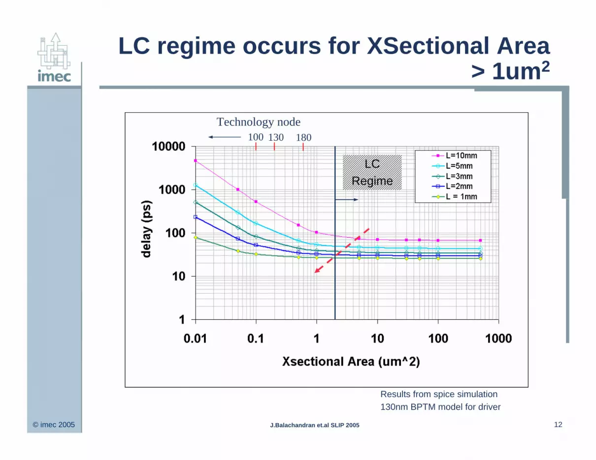
LC regime occurs for XSectional Area > 1um2
LCRegime
130100Technology node
180
Results from spice simulation130nm BPTM model for driver

© imec 2005 13J.Balachandran et.al SLIP 2005
Wiring sizing outperform Repeater Insertion
• Diminishing returns with repeaters for increasing wire x-section• Below red line wire sizing outperforms repeaters

© imec 2005 14J.Balachandran et.al SLIP 2005
Wide Gap in the interconnect Hierarchy
Interconnect gap
LocalSemi-global
Global
On-chip
PCB
Adv.PCB
Cross sectional Area - µm2
Fat wires on-chip?– Technologically challenging– Signal integrity– Cost
130 100
Technology node180

© imec 2005 15J.Balachandran et.al SLIP 2005
Bridging the Interconnect gap with Wafer Level Packaging
LocalSemi-global
Global
On-chip
PCB
Adv.PCB
Cross sectional Area - µm2
Fat wires on-chip?– Technologically challenging– Signal integrity– Cost
MCM
WLP
130 100
Technology node180

© imec 2005 16J.Balachandran et.al SLIP 2005
WLP Concept
BEOL
FEOL
WLP
• WLP wiring layers are post processed on top of active wafer• Modular approach to wire stacking• Thick low-k ILD with larger metal cross section
130nm test chip

© imec 2005 17J.Balachandran et.al SLIP 2005
WLP enables higher wiring density than conventional packages
Conventional Package wiring WLP wiring
WLP• uses vias for inter layer connection• Package wiring layers form a part of chip

© imec 2005 18J.Balachandran et.al SLIP 2005
WLP Technology in our Test chips
2 user routable layersCu metals and low-k BCB dielectric (εr = 2.65)Two process configurations
Config1 – 6 masks, IMPS T-linesConfig2 – 8 masks, Ta205 decoupling capacitors, Microstrip T-lines

© imec 2005 19J.Balachandran et.al SLIP 2005
Outline
(Interconnect) Challenges in Nanometer Era
Review of contemporary solutions
Interconnect Scaling & Motivation for Packaging Approach
WLP Technology
Performance Comparison
Applications
Conclusion

© imec 2005 20J.Balachandran et.al SLIP 2005
Metrics for Package-BEOL Comparison
Bandwidth (BW)
– No. of bits transmitted per second per wire
BW density
– BW across unit routing area
– Measure of wiring density
Latency
– Delay with respect to clock period
Power

© imec 2005 21J.Balachandran et.al SLIP 2005
3-7x BW improvement possible with Packaging Approach
FFFF
Tb
Ts01Ts10
Tp
η ≥ 1 - signal integrity factor
WLP T-line
On-chip global line
Line length = 5mmη = 1.3
Package Bandwidthis limited by register setupand hold times
⎟⎠⎞
⎜⎝⎛ +
=
2
1
01TpT
BWs
RC
η ( )psLC TT
BW+
=01
1η

© imec 2005 22J.Balachandran et.al SLIP 2005
Package Level Interconnects Enable Single Cycle Communication
clkFDLT *int=LT = latencyDint = interconnect delayFclk = Clock frequency specified by ITRS
Line length = 10mm
On-chip global line
Package T-line

© imec 2005 23J.Balachandran et.al SLIP 2005
Significant Power savings with Package level Interconnects
tto
r
onchipi
lineTpkg
globalchip
CRC
CZoCC
+
= −
−−
−
ε
**75.1
For comparing power, Capacitance ratio is derived as
Zo = characteristic impedance of transmission lineCi-on chip =On-chip global interconnect capacitanceRt,Ct – minimum sized driver output resistance and input capacitance
Power saving Per bit
Zo = 75Ω

© imec 2005 24J.Balachandran et.al SLIP 2005
Bandwidth density is lowered in Package level Interconnects
PBW
SWBWBD =+
=
WLP T-line
On-chip global line
Line length = 5mm

© imec 2005 25J.Balachandran et.al SLIP 2005
Outline
(Interconnect) Challenges in Nanometer Era
Review of contemporary solutions
Interconnect Scaling & Motivation for Packaging Approach
WLP Technology
Performance Comparison
Applications
Conclusion

© imec 2005 26J.Balachandran et.al SLIP 2005
Interconnect Options:Memory buses
Off-chip BW is limited – strong trend for more on-chip memories
Micrograph of aleading ProcessorSource: ISSC 2002
• WLP interconnects allow low latency memory accesses spread across the die• Repeater less communication enables routing over hard macro blocks• Can be routed over sensitive analogue blocks• Flexible floor planning• Low power
Memories occupies significant die area

© imec 2005 27J.Balachandran et.al SLIP 2005
Interconnect Options:Inter Tile Communication
• Exploit LC Transmission line properties of WLP interconnects• NOC or Bus ?

© imec 2005 28J.Balachandran et.al SLIP 2005
Interconnect Options:Clock distribution
• First few levels of clock trees can be in WLP• Inherent low rise time as compared to on-chip lines• Low latency -> relaxed skew tolerance• Low power
© imec 2005 29J.Balachandran et.al SLIP 2005
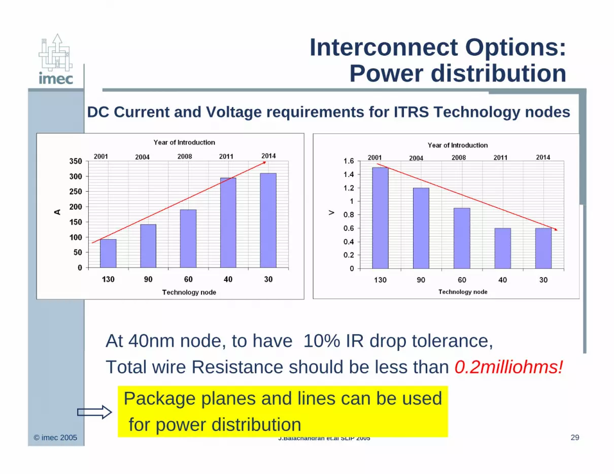
Interconnect Options: Power distribution
DC Current and Voltage requirements for ITRS Technology nodes
At 40nm node, to have 10% IR drop tolerance, Total wire Resistance should be less than 0.2milliohms!
Package planes and lines can be usedfor power distribution

© imec 2005 30J.Balachandran et.al SLIP 2005
Conclusion
Global interconnect delay and power delivery issues dominate nano-CMOS designs
Reverse scaling enabled by WLP Packaging approach is promising :
– Extends on-chip Wiring hierarchy
– High BW @ low power and latencies
– Simultaneously address signal and power distribution
– However limited wiring density
Options
– Memory buses, Intertile Communication, Clock and Power distribution

© imec 2005 31J.Balachandran et.al SLIP 2005
Thank you
Acknowledgements:Scott List, Maarten Kuijk,Franky Cathoor, Philip Christie,Mandeep Bamal