Embed Size (px)
Citation preview
ARTICLE IN PRESS
Microelectronics Journal 40 (2009) 928–938
Contents lists available at ScienceDirect
Microelectronics Journal
0026-26
doi:10.1
� Corr
E-m
sminaei
journal homepage: www.elsevier.com/locate/mejo
Novel floating simulated inductors with wider operating-frequency ranges
Erkan Yuce a, Shahram Minaei b,�
a Pamukkale University, Department of Electrical and Electronics Engineering, 20070 Kinikli-Denizli, Turkeyb Dogus University, Department of Electronics and Communications Engineering, Acibadem, Kadikoy 34722, Istanbul, Turkey
a r t i c l e i n f o
Article history:
Received 28 July 2008
Received in revised form
20 December 2008
Accepted 23 December 2008Available online 28 February 2009
Keywords:
Floating inductor simulator
Current conveyor
Analog filter
CMOS
92/$ - see front matter & 2009 Elsevier Ltd. A
016/j.mejo.2008.12.002
esponding author. Tel.: +90 216 3271104.
ail addresses: [email protected] (E. Yu
@dogus.edu.tr (S. Minaei).
a b s t r a c t
In this paper, a number of simulated floating inductors (FIs) employing second-generation current
conveyor (CCII), current-feedback operational amplifier (CFOA), differential voltage current conveyor
(DVCC) and differential difference current conveyor (DDCC) are proposed. They employ only a grounded
capacitor; accordingly, they are suitable for integrated circuit (IC) implementation. Some of the
developed FI simulators demonstrate the feature of improved low-frequency performance while
the other ones suffer from the Z/Y terminal parasitic resistors bringing extra series resistors to the
inductances of the simulated FIs. Two novel methods for reducing/eliminating the unwanted series
resistance in equivalent inductances of the FIs are developed, one of which is called the direct design
technique accomplished by adjusting the resistive component/components of the FIs. The series
resistors of the FIs affecting their low-frequency performance can be canceled by adding floating
negative resistors in series, which is another method. Three of the presented FIs as examples are chosen
in order to verify the developed method, perform their simulations and show their performance.
& 2009 Elsevier Ltd. All rights reserved.
1. Introduction
Operational amplifiers (OAs) as basic building block have beenpopular in the market since the advent of the first analogintegrated circuit (IC). Nevertheless, there is a new impulsetowards the current-mode (CM) circuits instead of voltage-mode(VM) ones, because CM configurations can overcome the restric-tion of the constant gain-bandwidth product and the trade-offbetween speed and bandwidth. In other words, the performanceof the CM configurations is improved in terms of low-voltagecharacteristics, slew rate and bandwidth. A current conveyor (CC)as an alternative to the OA is a fundamental building block used inanalog circuit design [1].
Although physical inductors are used for analog filter andoscillator designs, they are usually unwanted passive componentsin most of the electronic configurations because their character-istics are far from the ideal element behaviors. In addition,they occupy larger chip area when compared to other passivecomponents such as resistors and capacitors. The most widelyused inductor in IC is planar spiral whereas it occupies a large chiparea, and has low quality factor (Q) [2]. Fortunately, CCs are widelyused in the design of simulated floating inductors (FIs) [3–24].FI simulators can be divided into two categories according to theuse of generation of active components. The first generation of FIs
ll rights reserved.
ce),
called active RC FI simulators is composed of OAs, whilethe second-generation FIs use CCs such as second-generationcurrent conveyors (CCIIs), current-feedback operational amplifiers(CFOAs), differential voltage current conveyors (DVCCs) [25] anddifferential difference current conveyors (DDCCs) [26]. It is wellknown that second-generation FIs are superior to first-generationones owing to the fact that they operate at high frequencies, anddo not need passive component matching conditions [3].
In this paper, eight ideally lossless FIs employing two to fourresistors and a grounded capacitor are proposed. All the proposedFI simulators use CCII, CFOA, DVCC and DDCC as active element.Five of the realized FIs have improved low-frequency perfor-mance. Three of the FI simulators employ only grounded passivecomponents and two of the simulated FIs are free from passivecomponent matching requirements.
In the literature, some parasitic impedance effect-reductionmethods for the FIs [24] and grounded inductors [27] werepreviously developed. However, the inductors in [24] and [27] usesix and three plus-type CCIIs, respectively.
Contrary to the FI proposed in [24] employing six activedevices, the presented FIs with reduced Z and Y terminal parasiticresistors effective at low frequencies employ only two or threeactive components. In other words, the use of active componentsis decreased 66.6% and 50%, respectively. Apart from this, somemethods for improving high-frequency performances of activedevices have been presented in the open literature [28–30].
A universal filter with three inputs and one output as well as amultifunction filter with single input and three outputs composedof a FI simulator, a capacitor and a resistor are introduced to
ARTICLE IN PRESS
E. Yuce, S. Minaei / Microelectronics Journal 40 (2009) 928–938 929
exhibit the performance of the proposed configurations and toconfirm the theory. For this purpose, three of the proposed FIs arechosen as examples to accomplish their experimental tests andsimulations using SPICE program.
The rest of the paper is organized as follows: the proposed FIsand their active components are treated in Section 2. Non-idealityeffects such as non-ideal gain and parasitic impedance effectsare discussed in Sections 3 and 4, respectively. In Section 4, twonew methods for improving the low-frequency performanceof the FIs are developed. Universal and multifunction filterdesign methods using FIs are given in Section 5. Simulation andexperimental results to confirm the theory are given in Section 7.Finally, the paper is concluded in Section 8.
Fig. 3. Electrical symbol of a floating inductor simulator.
2. Description of the floating inductors
Dual output DDCC as a versatile active device, whose electricalsymbol is shown in Fig. 1, can be expressed by the followingmatrix equation:
IY1
IY2
IY3
VX
IZþ
IZ�
26666666664
37777777775¼
YY1ðsÞ 0 0 0 0 0
0 YY2ðsÞ 0 0 0 0
0 0 YY3ðsÞ 0 0 0
b1ðsÞ �b2ðsÞ b3ðsÞ ZxðsÞ 0 0
0 0 0 aðsÞ YZþðsÞ 0
0 0 0 �gðsÞ 0 YZ�ðsÞ
26666666664
37777777775
VY1
VY2
VY3
IX
VZþ
VZ�
26666666664
37777777775
(1)
Ideally the non-ideal gains a(s) ¼ g(s) ¼ bi(s) ¼ 1 (i ¼ 1, 2, 3)and parasitic admittances/impedances YY1(s) ¼ YY2(s) ¼ YY3(s) ¼Zx(s) ¼ 0. Apart from this, a DVCC can be easily obtained from theDDCC by grounding one of the Y1 or Y3 terminals.
Likewise, defining matrix equation of the CFOA whoseelectrical symbol depicted in Fig. 2 can be given as
IZ
IY
VX
VW
266664
377775 ¼
aðsÞ 0 0 YZðsÞ
0 0 YY ðsÞ 0
ZxðsÞ 0 bðsÞ 0
0 ZwðsÞ 0 ZðsÞ
266664
377775
IX
IW
VY
VZ
266664
377775 (2)
Fig. 1. Electrical symbol of a dual-output DDCC.
X
Y
Ix
Iy
X
Y
CCII+ Z BufferIw
W
CFOA (AD844)
Z
Iz
Fig. 2. Symbolic representation of a CFOA composed of a CCII+ and a buffer.
Similarly, a CCII can be easily implemented from the DDCC bygrounding its Y2 and Y3 terminals. On the other hand, electricalsymbol of a FI simulator is shown in Fig. 3, and it is represented bythe following short-circuit admittance matrix:
½Y � ¼1
sLeq
1 �1
�1 1
� �(3)
A collection of FI simulators is shown in Figs. 4–11. Theproposed FIs in Figs. 5–11 are novel, while the one in Fig. 4 isderived and modified from the one reported in [4]. In fact the FI inFig. 4 can be constructed with three AD844s [31] while theoriginal one reported in [4] needs four AD844s for its realization.Moreover, the FIs in Figs. 7 and 8 are different versions of the onesin Figs. 5 and 6, respectively. FIs in Figs. 4 and 5 have no passivecomponent matching constraints. Nevertheless, the ones inFigs. 7–11 require passive component matching conditions inorder to succeed the cancellation of unwanted parasitic impe-dances effective at low frequencies.
The application of straightforward analysis to the proposed FIsimulators in Figs. 4–11 ideally gives the following matrix equation:
I1
I2
" #¼
1
sCR1R2
1 �1
�1 1
� �V1
V2
" #(4)
Fig. 4. The first proposed ideally lossless FI employing a grounded capacitor.
Fig. 5. The second ideally lossless FI employing a grounded capacitor.
ARTICLE IN PRESS
Fig. 6. The third ideally lossless FI employing a grounded capacitor.
Fig. 7. The fourth introduced FI with improved low-frequency performances.
Fig. 8. The fifth realized FI with improved low-frequency performances.
Fig. 9. The sixth presented FI with improved low-frequency performances.
Fig. 10. The seventh FI with improved low-frequency performances.
Fig. 11. The eighth FI with improved low-frequency performances where the
Z terminals of the first DDCC are grounded.
E. Yuce, S. Minaei / Microelectronics Journal 40 (2009) 928–938930
Note that in order to obtain the matrix Eq. (4) for some of the FIsin Figs. 4–11, the following matching constraint/constraintsshould be provided:
(i)
R2 ¼ R3 must be chosen for the FIs in Figs. 6 and 9. (ii) R1 ¼ R3 must be chosen for the FIs in Figs. 7 and 10.(iii)
R1 ¼ R4 and R2 ¼ R3 must be chosen for the FI in Fig. 8. (iv) R1 ¼ R2 must be chosen for the FI in Fig. 11.The matrix equation in (4), as an example, for the FI simulator inFig. 4 can be derived by the help of the following equations:
I1 ¼ �I2 (5a)
ARTICLE IN PRESS
E. Yuce, S. Minaei / Microelectronics Journal 40 (2009) 928–938 931
I1 ¼V3
R2(5b)
V1 � V2
R1¼ sCV3 (5c)
As a second example, consider the circuit in Fig. 6. AssumingDVCC+s to be ideal, one can write the following equations:
V3
R3¼ �I2 (6a)
I1 ¼V3
R2(6b)
V1 � V2
R1¼ sCV3 (6c)
Combining Eqs. (6a), (6b) and (6c) will result in the followingequation:
I1 ¼1
sCR1R2ðV1 � V2Þ
I2 ¼�1
sCR1R3ðV1 � V2Þ
9=; (7)
If R2 ¼ R3, the ideal matrix equation of (4) is obtained.Otherwise the circuit gives different equivalent inductances seenfrom the first and second terminals of the circuit. For instance, ifthe second terminal of the circuit in Fig. 6 is grounded (V2 ¼ 0),the equivalent grounded inductance seen from the first terminal isLeq ¼ CR1R2, while if the first terminal is grounded (V1 ¼ 0) theequivalent grounded inductance seen from the second terminal isLeq ¼ CR1R3.
Finally, note that all of the introduced FIs use a groundedcapacitor; accordingly they are advantageous from the IC realiza-tion point of view [32,33]. Further, the proposed FIs depicted inFigs. 6, 8 and 10 employ both grounded resistors and capacitors,which are ideal for the IC design [32–34]. Alternatively, therealized simulated FIs shown in Figs. 4, 5 and 11 use a minimumnumber of passive components, i.e. two resistors and a groundedcapacitor. All of the introduced FIs in Figs. 4–11 with no capacitorconnected in series to the X terminals of the CCIIs/DVCC/DDCCand W terminals of the CFOA can be operated at higherfrequencies [35,36].
3. Non-ideal gain effects
It is seen from the matrix equation in (1) that a(s) and g(s)correspond to frequency-dependent non-ideal current gains.Similarly, bi(s) corresponds to frequency-dependent non-idealvoltage gain. The frequency-dependent non-ideal gains of theDDCC, using a single-pole-model [37,38] in the jo domain, can bedefined as
aðjoÞ ¼ ao
�1þ
jooa
� �(8a)
biðjoÞ ¼ boi
�1þ
joobi
� �(8b)
gðjoÞ ¼ go
�1þ
joog
� �(8c)
In (8b) i ¼ 1, 2, 3 and the pole frequencies oa, obi and ogin (8a)–(8c) depend on the technology parameters, and ideallyequal to infinity. The operation frequency of the presented FIs inFigs. 5–11 can be defined as f5min{oa, obi, og}. Also, the DC gainsao, boi and go are ideally equal to unity, and can be described as
follows:
ao ¼ 1þ �a (9a)
boi ¼ 1þ �bi (9b)
go ¼ 1þ �g (9c)
where ea (9ea951) and eg (9eg951) are current-tracking errors andebi (9ebi951) is called as voltage-tracking error.
As an example, if non-ideal gain effects of the FI in Fig. 4 aretaken into account, by applying straightforward analysis to the FIof Fig. 4, the following matrix equation is obtained:
I1
I2
" #¼
a1b3
sCR1R2
a2b1 �a2Z3
�a3b1 a3Z3
" #V1
V2
" #(10)
Here, the subscripts of the parameters a, b, and Z represent thecorresponding active device. Also, a is the current gain betweenX and Z terminals of the CCII+/CFOA. b and Z are the correspond-ing voltage gains between Y and X terminals of the CCII+/CFOAand between Z and W terminals of the CFOA, respectively.Likewise, Z using a single-pole model can be expressed as
ZðjoÞ ¼ Zo
�1þ
jooZ
� �(11)
where Zo ¼ 1+eZ and eZ(9eZ951) is a voltage-tracking error.Therefore, the operation frequency of the proposed FI in Fig. 4can be defined as f5min{oa, ob, og, oZ}.
4. Parasitic impedance effects
The series X terminal parasitic impedance Zx(s), parallelY terminal parasitic impedances Yl(s) (l ¼ 1, 2, 3), Z terminalparasitic impedances YZ+(s), YZ�(s) and series W terminal parasiticimpedance Zw(s) in (1) and (2) can be expressed as
ZxðsÞ ¼ Rx þ sLx (12a)
YlðsÞ ¼ sCl þ1
Rl(12b)
YZþðsÞ ¼ sCZþ þ1
RZþ(12c)
YZ�ðsÞ ¼ sCZ� þ1
RZ�(12d)
ZwðsÞ ¼ Rw þ sLw (12e)
where ZxffiRx at low and medium frequencies. We assumethat ZxffiRx for operating frequency f5Rx/Lx obtained using (12a).Moreover, the parasitic resistances Rx, Rl and RZ besides parasiticcapacitances Cl and CZ bring extra components to the inductancesof the FI simulators. The equivalent circuit for the FIs in Figs. 4–11considering their parasitic impedances is given in Fig. 12.
The equivalent circuit in Fig. 12 can be defined by the followingmatrix equation:
I1
I2
" #¼
1
Zp1kZeq�
1
Zeq
�1
Zeq
1
Zp2kZeq
26664
37775
V1
V2
" #(13)
where
Zpj ¼1
1=Rpj þ sCpj; ðj ¼ 1; 2Þ (14a)
Zeq ¼ sLeq þ Req (14b)
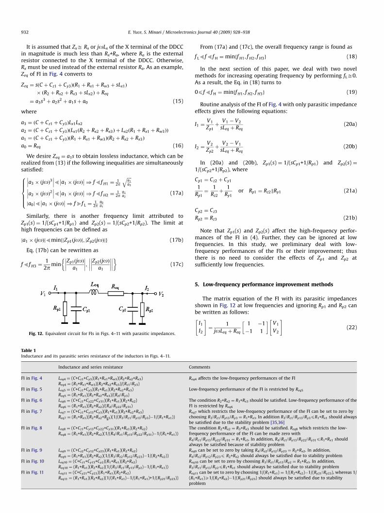
ARTICLE IN PRESS
E. Yuce, S. Minaei / Microelectronics Journal 40 (2009) 928–938932
It is assumed that Zxffi Rx or joLx of the X terminal of the DDCCin magnitude is much less than Rx+Ra, where Ra is the externalresistor connected to the X terminal of the DDCC. Otherwise,Rx must be used instead of the external resistor Ra. As an example,Zeq of FI in Fig. 4 converts to
Zeq ¼ sðC þ Cz1 þ Cy3ÞðR1 þ Rx1 þ Rw3 þ sLx1Þ
� ðR2 þ Rx2 þ Rx3 þ sLx2Þ þ Req
¼ a3s3 þ a2s2 þ a1sþ a0 (15)
where
a3 ¼ ðC þ Cz1 þ Cy3ÞLx1Lx2
a2 ¼ ðC þ Cz1 þ Cy3ÞðLx1ðR2 þ Rx2 þ Rx3Þ þ Lx2ðR1 þ Rx1 þ Rw3ÞÞ
a1 ¼ ðC þ Cz1 þ Cy3ÞðR1 þ Rx1 þ Rw3ÞðR2 þ Rx2 þ Rx3Þ
a0 ¼ Req (16)
We desire Zeq ¼ a1s to obtain lossless inductance, which can berealized from (13) if the following inequalities are simultaneouslysatisfied:
a3 � ðjoÞ3��� ���5 a1 � ðjoÞ
�� ��) f5f H1 ¼1
2p
ffiffiffiffia1a3
qa2 � ðjoÞ2��� ���5 a1 � ðjoÞ
�� ��) f5f H2 ¼1
2pa1a2
a0j j5 a1 � ðjoÞ�� ��) fbf L ¼
12p
a0a1
8>>>><>>>>:
(17a)
Similarly, there is another frequency limit attributed toZp1(s) ¼ 1/(sCp1+1/Rp1) and Zp2(s) ¼ 1/(sCp2+1/Rp2). The limit athigh frequencies can be defined as
ja1 � ðjoÞj5minfjZp1ðjoÞj; jZp2ðjoÞjg (17b)
Eq. (17b) can be rewritten as
f5f H3 ¼1
2pmin
Zp1ðjoÞa1
��������; Zp2ðjoÞ
a1
��������
��������
(17c)
Fig. 12. Equivalent circuit for FIs in Figs. 4–11 with parasitic impedances.
Table 1Inductance and its parasitic series resistance of the inductors in Figs. 4–11.
Inductance and series resistance Co
FI in Fig. 4 Leq4 ¼ (C+Cz1+Cy3)(R1+Rx1+Rw3)(R2+Rx2+Rx3) Req
Req4 ¼ (R1+Rx1+Rw3)(R2+Rx2+Rx3)/(Rz1JRy3)
FI in Fig. 5 Leq5 ¼ (C+Cz1+Cy3)(R1+Rx1)(R2+Rx2+Rx3) Lo
Req5 ¼ (R1+Rx1)(R2+Rx2+Rx3)/(RzlJRy3)
FI in Fig. 6 Leq6 ¼ (C+Cz1+Cy22+Cy31)(R1+Rx1)(R2+Rx2) Th
FIReq6 ¼ (R1+Rx1)(R2+Rx2)/(RzlJRy22JRy31)
FI in Fig. 7 Leq7 ¼ (C+Cz1+Cy13+Cy3)(R1+Rx1)(R2+Rx2+Rx3) Req
ch
be
Req7 ¼ (R1+Rx1)(R2+Rx2+Rx3)(1/(R3JRz1JRy13JRy3)�1/(R1+Rx1))
FI in Fig. 8 Leq8 ¼ (C+Cz1+Cy13+Cy22+Cy31)(R1+Rx1)(R2+Rx2) Th
fre
R4
alw
Req8 ¼ (R1+Rx1)(R2+Rx2)(1/(R4JRz1JRy13JRy22JRy31)�1/(R1+Rx1))
FI in Fig. 9 Leq9 ¼ (C+Cz2+Cy12+Cy23)(R1+Rx1)(R2+Rx2) Req
R4Req9 ¼ (R1+Rx1)(R2+Rx2)(1/(R3JRz2JRy12JRy23)�1/(R2+Rx2))
FI in Fig. 10 Leq10 ¼ (C+Cz1+Cy13+Cy2)(R1+Rx1)(R2+Rx2) Req
R3Req10 ¼ (R1+Rx1)(R2+Rx2)(1/(R3JRz1JRy13JRy2)�1/(R1+Rx1))
FI in Fig. 11 Leq11 ¼ (C+Cy21+Cy23)(R1+Rx1)(R2+Rx2) Req
(R
pr
Req11 ¼ (R1+Rx1)(R2+Rx2)(1/(R1+Rx1)�1/(R1+Rx1)+1/(Ry21JRy23))
From (17a) and (17c), the overall frequency range is found as
f L5f5f H ¼minff H1; f H2; f H3g (18)
In the next section of this paper, we deal with two novelmethods for increasing operating frequency by performing fLffi0.As a result, the Eq. in (18) turns to
0pf5f H ¼ minff H1; f H2; f H3g (19)
Routine analysis of the FI of Fig. 4 with only parasitic impedanceeffects gives the following equations:
I1 ¼V1
Zp1þ
V1 � V2
sLeq þ Req(20a)
I2 ¼V2
Zp2þ
V2 � V1
sLeq þ Req(20b)
In (20a) and (20b), Zp1(s) ¼ 1/(sCp1+1/Rp1) and Zp2(s) ¼1/(sCp2+1/Rp2), where
Cp1 ¼ Cz2 þ Cy1
1
Rp1¼
1
Rz2þ
1
Ry1or Rp1 ¼ Rz2kRy1 (21a)
Cp2 ¼ Cz3
Rp2 ¼ Rz3 (21b)
Note that Zp1(s) and Zp2(s) affect the high-frequency perfor-mances of the FI in (4). Further, they can be ignored at lowfrequencies. In this study, we preliminary deal with low-frequency performances of the FIs or their improvement; thusthere is no need to consider the effects of Zp1 and Zp2 atsufficiently low frequencies.
5. Low-frequency performance improvement methods
The matrix equation of the FI with its parasitic impedancesshown in Fig. 12 at low frequencies and ignoring Rp1 and Rp2 canbe written as follows:
I1
I2
" #¼
1
joLeq þ Req
1 �1
�1 1
� �V1
V2
" #(22)
mments
4 affects the low-frequency performances of the FI
w-frequency performance of the FI is restricted by Req5
e condition R2+Rx2 ¼ R3+Rx3 should be satisfied. Low-frequency performance of the
is restricted by Req6
7 which restricts the low-frequency performance of the FI can be set to zero by
oosing R3JRz1JRy13JRy3 ¼ R1+Rx1. In addition R3JRz1JRy13JRy3pR1+Rx1 should always
satisfied due to the stability problem [35,36]
e condition R2+Rx2 ¼ R3+Rx3 should be satisfied. Req8 which restricts the low-
quency performance of the FI can be made zero with
JRz1JRy13JRy22JRy31 ¼ R1+Rx1. In addition, R4JRz1JRy13JRy22JRy31pR1+Rx1 should
ays be satisfied because of stability problem
9 can be set to zero by taking R4JRz2JRy12JRy23 ¼ R2+Rx2. In addition,
JRz2JRy12JRy23p R2+Rx2 should always be satisfied due to stability problem
10 can be set to zero by choosing R3JRz1JRy13JRy2 ¼ R1+Rx1. In addition,
JRz1JRy13JRy2pR1+Rx1 should always be satisfied due to stability problem
11 can be set to zero by choosing 1/(R1+Rx1) ¼ 1/(R2+Rx2)�1/(Ry21JRy23), whereas 1/
1+Rx1)X1/(R2+Rx2)�1/(Ry21JRy23) should always be satisfied due to stability
oblem
ARTICLE IN PRESS
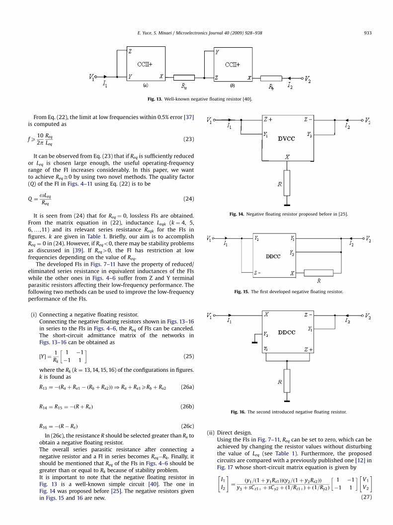
Fig. 13. Well-known negative floating resistor [40].
Fig. 14. Negative floating resistor proposed before in [25].
Fig. 15. The first developed negative floating resistor.
E. Yuce, S. Minaei / Microelectronics Journal 40 (2009) 928–938 933
From Eq. (22), the limit at low frequencies within 0.5% error [37]is computed as
fX10
2pReq
Leq(23)
It can be observed from Eq. (23) that if Req is sufficiently reducedor Leq is chosen large enough, the useful operating-frequencyrange of the FI increases considerably. In this paper, we wantto achieve Reqffi0 by using two novel methods. The quality factor(Q) of the FI in Figs. 4–11 using Eq. (22) is to be
Q ¼oLeq
Req(24)
It is seen from (24) that for Req ¼ 0, lossless FIs are obtained.From the matrix equation in (22), inductance Leqk (k ¼ 4, 5,6,y,11) and its relevant series resistance Reqk for the FIs infigures. k are given in Table 1. Briefly, our aim is to accomplishReq ¼ 0 in (24). However, if Reqo0, there may be stability problemsas discussed in [39]. If Req40, the FI has restriction at lowfrequencies depending on the value of Req.
The developed FIs in Figs. 7–11 have the property of reduced/eliminated series resistance in equivalent inductances of the FIswhile the other ones in Figs. 4–6 suffer from Z and Y terminalparasitic resistors affecting their low-frequency performance. Thefollowing two methods can be used to improve the low-frequencyperformance of the FIs.
(i)
Fig. 16. The second introduced negative floating resistor.
Connecting a negative floating resistor.Connecting the negative floating resistors shown in Figs. 13–16in series to the FIs in Figs. 4–6, the Req of FIs can be canceled.The short-circuit admittance matrix of the networks inFigs. 13–16 can be obtained as
½Y � ¼1
Rk
1 �1
�1 1
� �(25)
where the Rk (k ¼ 13, 14, 15, 16) of the configurations in figures.k is found as
R13 ¼ �ðRa þ Rx1 � ðRb þ Rx2ÞÞ ) Ra þ Rx1XRb þ Rx2 (26a)
R14 ¼ R15 ¼ �ðRþ RxÞ (26b)
R16 ¼ �ðR� RxÞ (26c)
In (26c), the resistance R should be selected greater than Rx toobtain a negative floating resistor.The overall series parasitic resistance after connecting anegative resistor and a FI in series becomes Req�Rk. Finally, itshould be mentioned that Req of the FIs in Figs. 4–6 should begreater than or equal to Rk because of stability problem.It is important to note that the negative floating resistor inFig. 13 is a well-known simple circuit [40]. The one inFig. 14 was proposed before [25]. The negative resistors givenin Figs. 15 and 16 are new.
(ii)
Direct design.Using the FIs in Fig. 7–11, Req can be set to zero, which can beachieved by changing the resistor values without disturbingthe value of Leq (see Table 1). Furthermore, the proposedcircuits are compared with a previously published one [12] inFig. 17 whose short-circuit matrix equation is given byI1
I2
" #¼
ðy1=ð1þ y1Rx1ÞÞðy2=ð1þ y2Rx2ÞÞ
y3 þ sCz1þ þ sCy2 þ ð1=Rz1þÞ þ ð1=Ry2Þ
1 �1
�1 1
� �V1
V2
" #
(27)
ARTICLE IN PRESS
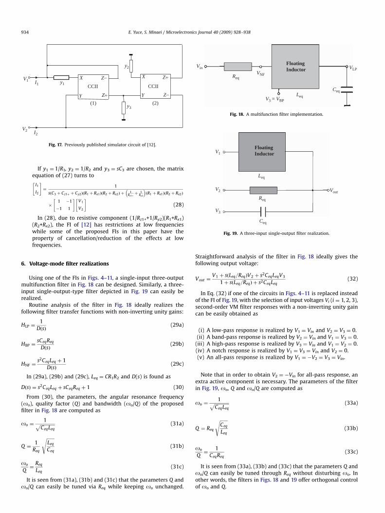
Vin
ReqVNF
V3 = VBPLeq
Ceq
VLPFloatingInductor
Fig. 18. A multifunction filter implementation.
Ceq
Vout
V1
V2
V3
Leq
FloatingInductor
Req
Fig. 19. A three-input single-output filter realization.
V1
y3
y2
I1Z+X
CCII
Y
XCCII
(1)
y1
Z+(2)
Y Z−
Z−
V2 I2
Fig. 17. Previously published simulator circuit of [12].
E. Yuce, S. Minaei / Microelectronics Journal 40 (2009) 928–938934
If y1 ¼ 1/R1, y2 ¼ 1/R2 and y3 ¼ sC3 are chosen, the matrixequation of (27) turns to
I1
I2
" #¼
1
sðC3 þ Cz1þ þ Cy2ÞðR1 þ Rx1ÞðR2 þ Rx2Þ þ1
Rz1þþ 1
Ry2
� �ðR1 þ Rx1ÞðR2 þ Rx2Þ
�1 �1
�1 1
" #V1
V2
" #(28)
In (28), due to resistive component (1/Rz1++1/Ry2)(R1+Rx1)(R2+Rx2), the FI of [12] has restrictions at low frequencieswhile some of the proposed FIs in this paper have theproperty of cancellation/reduction of the effects at lowfrequencies.
6. Voltage-mode filter realizations
Using one of the FIs in Figs. 4–11, a single-input three-outputmultifunction filter in Fig. 18 can be designed. Similarly, a three-input single-output-type filter depicted in Fig. 19 can easily berealized.
Routine analysis of the filter in Fig. 18 ideally realizes thefollowing filter transfer functions with non-inverting unity gains:
HLP ¼1
DðsÞ(29a)
HBP ¼sCeqReq
DðsÞ(29b)
HNF ¼s2CeqLeq þ 1
DðsÞ(29c)
In (29a), (29b) and (29c), Leq ¼ CR1R2 and D(s) is found as
DðsÞ ¼ s2CeqLeq þ sCeqReq þ 1 (30)
From (30), the parameters, the angular resonance frequency(oo), quality factor (Q) and bandwidth (oo/Q) of the proposedfilter in Fig. 18 are computed as
oo ¼1ffiffiffiffiffiffiffiffiffiffiffiffiffi
CeqLeq
p (31a)
Q ¼1
Req
ffiffiffiffiffiffiffiLeq
Ceq
s(31b)
oo
Q¼
Req
Leq(31c)
It is seen from (31a), (31b) and (31c) that the parameters Q andoo/Q can easily be tuned via Req while keeping oo unchanged.
Straightforward analysis of the filter in Fig. 18 ideally gives thefollowing output voltage:
Vout ¼V1 þ sðLeq=ReqÞV2 þ s2CeqLeqV3
1þ sðLeq=ReqÞ þ s2CeqLeq(32)
In Eq. (32) if one of the circuits in Figs. 4–11 is replaced insteadof the FI of Fig. 19, with the selection of input voltages Vi (i ¼ 1, 2, 3),second-order VM filter responses with a non-inverting unity gaincan be easily obtained as
(i)
A low-pass response is realized by V1 ¼ Vin and V2 ¼ V3 ¼ 0. (ii) A band-pass response is realized by V2 ¼ Vin and V1 ¼ V3 ¼ 0.(iii)
A high-pass response is realized by V3 ¼ Vin and V1 ¼ V2 ¼ 0. (iv) A notch response is realized by V1 ¼ V3 ¼ Vin and V2 ¼ 0. (v) An all-pass response is realized by V1 ¼ �V2 ¼ V3 ¼ Vin.Note that in order to obtain V2 ¼ �Vin for all-pass response, anextra active component is necessary. The parameters of the filterin Fig. 19, oo, Q and oo/Q are computed as
oo ¼1ffiffiffiffiffiffiffiffiffiffiffiffiffi
CeqLeq
p (33a)
Q ¼ Req
ffiffiffiffiffiffiffiCeq
Leq
s(33b)
oo
Q¼
1
CeqReq(33c)
It is seen from (33a), (33b) and (33c) that the parameters Q andoo/Q can easily be tuned through Req without disturbing oo. Inother words, the filters in Figs. 18 and 19 offer orthogonal controlof oo and Q.
ARTICLE IN PRESS
Gai
n, d
B
ideal
5
0
-5
-10
-15
-20
-25
E. Yuce, S. Minaei / Microelectronics Journal 40 (2009) 928–938 935
7. Experimental test and simulation results
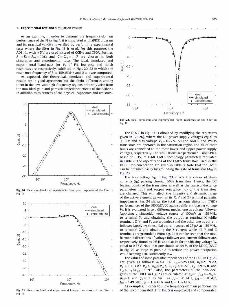
As an example, in order to demonstrate frequency-domainperformance of the FI in Fig. 4, it is simulated with SPICE programand its practical validity is verified by performing experimentaltests where the filter in Fig. 18 is used. For this purpose, theAD844s with 75 V are used instead of CCII+s and CFOA. Further,R1 ¼ R2 ¼ Req ¼ 1 kO and C ¼ Ceq ¼ 1 nF are chosen in bothsimulation and experimental tests. The ideal, simulated andexperimental band-pass (or V3 of FI), low-pass and notchresponses are, respectively, exhibited in Figs. 20–22 in which theresonance frequency of fo ¼ 159.15 kHz and Q ¼ 1 are computed.
As expected, the theoretical, simulated and experimentalresults are in good agreement but the slight differences amongthem in the low- and high-frequency regions primarily arise fromthe non-ideal gain and parasitic impedance effects of the AD844sin addition to tolerances of the physical capacitors and resistors.
5
0
-5
-10
-15
-20
-25
-30
Gai
n, d
B
104 105 106
idealsimulatedexperimental
Frequency, Hz
Fig. 20. Ideal, simulated and experimental band-pass responses of the filter in
Fig. 18.
Gai
n, d
B
104 105 106
idealsimulatedexperimental
Frequency, Hz
5
0
-5
-10
-15
-20
-25
-30
10
-35
-40
Fig. 21. Ideal, simulated and experimental low-pass responses of the filter in
Fig. 18.
simulatedexperimental
-30
-35104 105 106
Frequency, Hz
Fig. 22. Ideal, simulated and experimental notch responses of the filter in
Fig. 18.
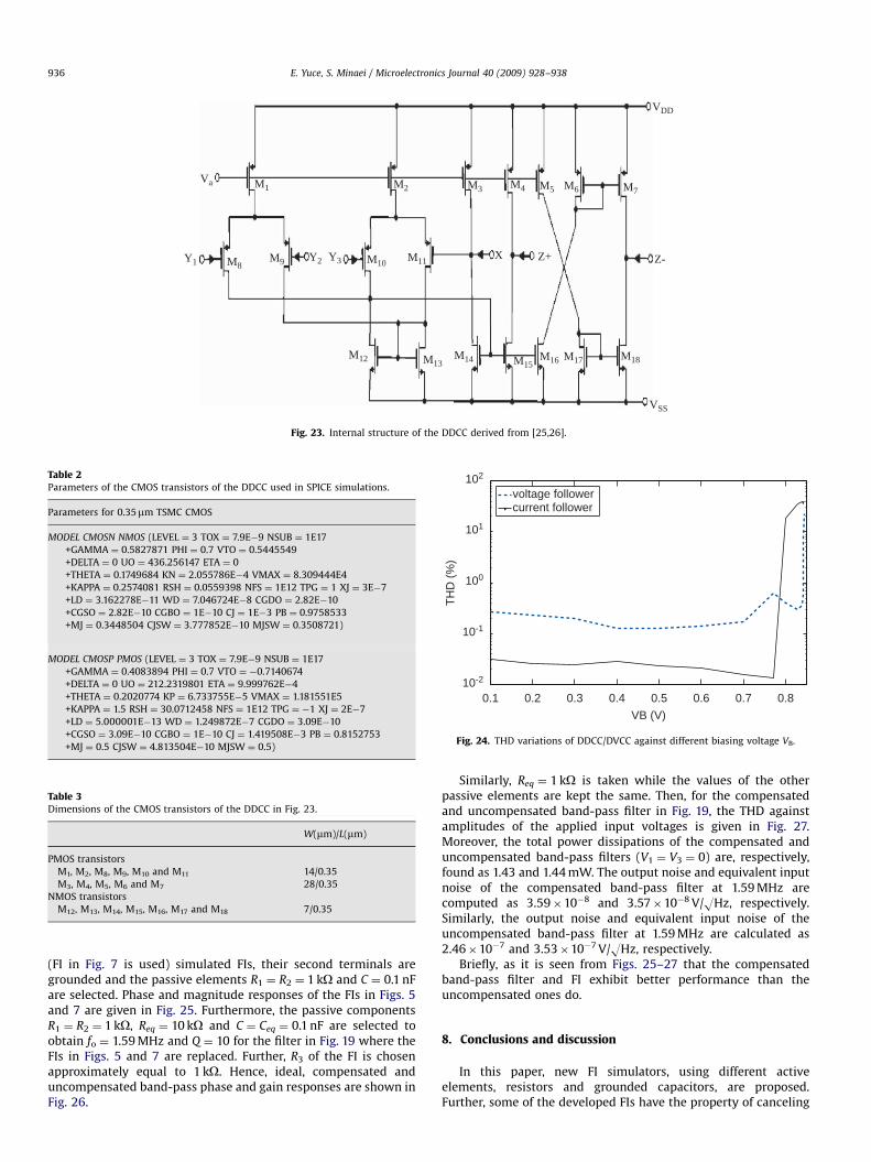
The DDCC in Fig. 23 is obtained by modifying the structuresgiven in [25,26], where the DC power supply voltages equal to71.5 V and bias voltage VB ¼ 0.77 V. All the NMOS and PMOStransistors are operated in the saturation region and all of theirbulks are connected to the most lower and upper power supplyvoltages, respectively. The simulations are performed using SPICEbased on 0.35mm TSMC CMOS technology parameters tabulatedin Table 2. The aspect ratios of the CMOS transistors used in theDDCC implementation are given in Table 3. Note that the DVCCcan be obtained easily by grounding the gate of transistor M10 inFig. 23.
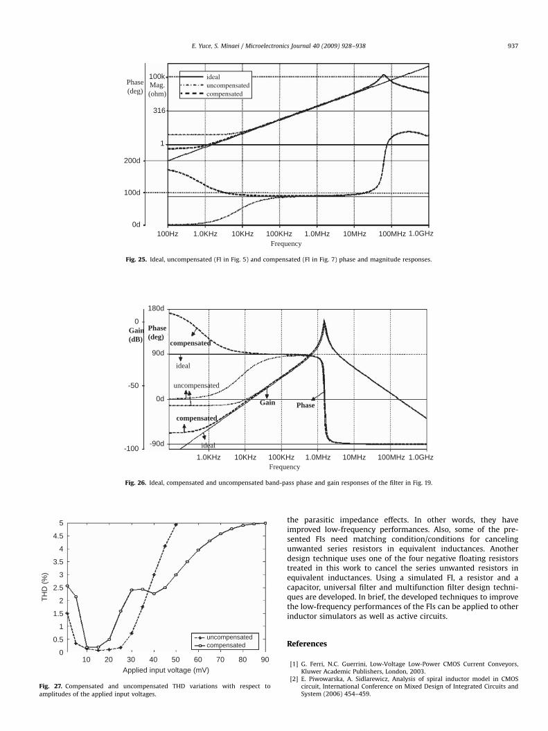
The bias voltage VB in Fig. 23 affects the values of draincurrents (ID) passing through MOS transistors. Hence, the DCbiasing points of the transistors as well as the transconductanceparameters (gm) and output resistance (ro) of the transistorsare changed. This will affect the linearity and dynamic rangeof the active element as well as its X, Y and Z terminal parasiticimpedances. Fig. 24 shows the total harmonic distortion (THD)performances of the DDCC/DVCC against different biasing voltageVB. It is evaluated in two different modes, one as voltage follower(applying a sinusoidal voltage source of 100 mV at 1.59 MHzto terminal Y1 and obtaining the output at terminal X whileterminals Z, Y2 and Y3 are grounded) and the other one as currentfollower (applying sinusoidal current source of 25mA at 1.59 MHzto terminal X and obtaining the Z current while all Y and Zterminals are grounded). From Fig. 24 it can be seen that the totalharmonic distortions of voltage follower and current follower are,respectively, found as 0.64% and 0.014% for the biasing voltage VB
equal to 0.77 V. Note that one should select VB of the DDCC/DVCCin Fig. 23 as large as possible to reduce the power dissipationwhile keeping THD sufficiently low.
The values of some parasitic impedances of the DDCC in Fig. 23are given as follows: Rxffi41.5O, Lx ¼ 525.1 nH, Rzffi215.9 kO,Rz�ffi180.3 kO, Ry1ffi Ry2ffiRy3ffiN, Cz+ffi10.5 fF, Cz�ffi9.87 fF andCy1ffiCy2ffiCy3 ¼ 15.9 fF. Also, the parameters of the non-idealgains of the DDCC in Fig. 23 are calculated as aoffi1, bo1ffi�bo2ffi
bo3ffi1 and goffi1.1 as well as fa ¼ 1.49 GHz, fb1 ¼1.58 GHz,fb2 ¼ 1.49 GHz, fb3 ¼ 1.39 GHz and fg ¼ 1.32 GHz.
As examples, in order to show frequency-domain performanceof the uncompensated (FI in Fig. 5 is employed) and compensated
ARTICLE IN PRESS
Va
Y1
M1
M8
M2 M3 M4 M5 M6 M7
VDD
Z-
M18
M9 M10 M11
M12 M13M14 M15
M16 M17
VSS
Y2 Y3 X Z+
Fig. 23. Internal structure of the DDCC derived from [25,26].
Table 2Parameters of the CMOS transistors of the DDCC used in SPICE simulations.
Parameters for 0.35mm TSMC CMOS
MODEL CMOSN NMOS (LEVEL ¼ 3 TOX ¼ 7.9E�9 NSUB ¼ 1E17
+GAMMA ¼ 0.5827871 PHI ¼ 0.7 VTO ¼ 0.5445549
+DELTA ¼ 0 UO ¼ 436.256147 ETA ¼ 0
+THETA ¼ 0.1749684 KN ¼ 2.055786E�4 VMAX ¼ 8.309444E4
+KAPPA ¼ 0.2574081 RSH ¼ 0.0559398 NFS ¼ 1E12 TPG ¼ 1 XJ ¼ 3E�7
+LD ¼ 3.162278E�11 WD ¼ 7.046724E�8 CGDO ¼ 2.82E�10
+CGSO ¼ 2.82E�10 CGBO ¼ 1E�10 CJ ¼ 1E�3 PB ¼ 0.9758533
+MJ ¼ 0.3448504 CJSW ¼ 3.777852E�10 MJSW ¼ 0.3508721)
MODEL CMOSP PMOS (LEVEL ¼ 3 TOX ¼ 7.9E�9 NSUB ¼ 1E17
+GAMMA ¼ 0.4083894 PHI ¼ 0.7 VTO ¼ �0.7140674
+DELTA ¼ 0 UO ¼ 212.2319801 ETA ¼ 9.999762E�4
+THETA ¼ 0.2020774 KP ¼ 6.733755E�5 VMAX ¼ 1.181551E5
+KAPPA ¼ 1.5 RSH ¼ 30.0712458 NFS ¼ 1E12 TPG ¼ �1 XJ ¼ 2E�7
+LD ¼ 5.000001E�13 WD ¼ 1.249872E�7 CGDO ¼ 3.09E�10
+CGSO ¼ 3.09E�10 CGBO ¼ 1E�10 CJ ¼ 1.419508E�3 PB ¼ 0.8152753
+MJ ¼ 0.5 CJSW ¼ 4.813504E�10 MJSW ¼ 0.5)
Table 3Dimensions of the CMOS transistors of the DDCC in Fig. 23.
W(mm)/L(mm)
PMOS transistors
M1, M2, M8, M9, M10 and M11 14/0.35
M3, M4, M5, M6 and M7 28/0.35
NMOS transistors
M12, M13, M14, M15, M16, M17 and M18 7/0.35
0.1 0.2 0.3 0.4 0.5 0.6 0.7 0.810-2
10-1
100
101
102
VB (V)
THD
(%)
voltage followercurrent follower
Fig. 24. THD variations of DDCC/DVCC against different biasing voltage VB.
E. Yuce, S. Minaei / Microelectronics Journal 40 (2009) 928–938936
(FI in Fig. 7 is used) simulated FIs, their second terminals aregrounded and the passive elements R1 ¼ R2 ¼ 1 kO and C ¼ 0.1 nFare selected. Phase and magnitude responses of the FIs in Figs. 5and 7 are given in Fig. 25. Furthermore, the passive componentsR1 ¼ R2 ¼ 1 kO, Req ¼ 10 kO and C ¼ Ceq ¼ 0.1 nF are selected toobtain fo ¼ 1.59 MHz and Q ¼ 10 for the filter in Fig. 19 where theFIs in Figs. 5 and 7 are replaced. Further, R3 of the FI is chosenapproximately equal to 1 kO. Hence, ideal, compensated anduncompensated band-pass phase and gain responses are shown inFig. 26.
Similarly, Req ¼ 1 kO is taken while the values of the otherpassive elements are kept the same. Then, for the compensatedand uncompensated band-pass filter in Fig. 19, the THD againstamplitudes of the applied input voltages is given in Fig. 27.Moreover, the total power dissipations of the compensated anduncompensated band-pass filters (V1 ¼ V3 ¼ 0) are, respectively,found as 1.43 and 1.44 mW. The output noise and equivalent inputnoise of the compensated band-pass filter at 1.59 MHz arecomputed as 3.59�10�8 and 3.57�10�8 V/OHz, respectively.Similarly, the output noise and equivalent input noise of theuncompensated band-pass filter at 1.59 MHz are calculated as2.46�10�7 and 3.53�10�7 V/OHz, respectively.
Briefly, as it is seen from Figs. 25–27 that the compensatedband-pass filter and FI exhibit better performance than theuncompensated ones do.
8. Conclusions and discussion
In this paper, new FI simulators, using different activeelements, resistors and grounded capacitors, are proposed.Further, some of the developed FIs have the property of canceling
ARTICLE IN PRESS
Phase(deg)
100kMag.(ohm)
316
1
200d
100d
0d100Hz
idealuncompensatedcompensated
1.0KHz 10KHz 100KHz 1.0MHz 10MHz 100MHz 1.0GHzFrequency
Fig. 25. Ideal, uncompensated (FI in Fig. 5) and compensated (FI in Fig. 7) phase and magnitude responses.
Gain(dB)
Phase(deg)
compensated
ideal
uncompensated
compensated
Gain Phase
1.0KHz 10KHz 100KHz 1.0MHz 10MHz 100MHz 1.0GHzFrequency
ideal
-50
-100
0
90d
0d
-90d
180d
Fig. 26. Ideal, compensated and uncompensated band-pass phase and gain responses of the filter in Fig. 19.
10 20 30 40 50 60 70 80 90Applied input voltage (mV)
5
4.5
4
3
2.5
2
1.5
1
0.5
0
3.5
THD
(%)
uncompensatedcompensated
Fig. 27. Compensated and uncompensated THD variations with respect to
amplitudes of the applied input voltages.
E. Yuce, S. Minaei / Microelectronics Journal 40 (2009) 928–938 937
the parasitic impedance effects. In other words, they haveimproved low-frequency performances. Also, some of the pre-sented FIs need matching condition/conditions for cancelingunwanted series resistors in equivalent inductances. Anotherdesign technique uses one of the four negative floating resistorstreated in this work to cancel the series unwanted resistors inequivalent inductances. Using a simulated FI, a resistor and acapacitor, universal filter and multifunction filter design techni-ques are developed. In brief, the developed techniques to improvethe low-frequency performances of the FIs can be applied to otherinductor simulators as well as active circuits.
References
[1] G. Ferri, N.C. Guerrini, Low-Voltage Low-Power CMOS Current Conveyors,Kluwer Academic Publishers, London, 2003.
[2] E. Piwowarska, A. Sidlarewicz, Analysis of spiral inductor model in CMOScircuit, International Conference on Mixed Design of Integrated Circuits andSystem (2006) 454–459.

ARTICLE IN PRESS
E. Yuce, S. Minaei / Microelectronics Journal 40 (2009) 928–938938
[3] M.C. Layos, I. Haritantis, On the derivation of current-mode floating inductors,International Journal of Circuit Theory and Applications 25 (1) (1997) 29–36.
[4] W. Kiranon, P. Pawarangkoon, Floating inductance simulation based oncurrent conveyors, Electronics Letters 33 (1997) 1748–1749.
[5] E. Yuce, O. Cicekoglu, S. Minaei, CCII-based grounded to floating immittanceconverter and a floating inductance simulator, Analog Integrated Circuits andSignal Processing 46 (3) (2006) 287–291.
[6] S. Minaei, E. Yuce, O. Cicekoglu, A versatile active circuit for realising floatinginductance capacitance FDNR and admittance converter, Analog IntegratedCircuits and Signal Processing 47 (2) (2006) 199–202.
[7] E. Yuce, S. Minaei, A modified CFOA and its applications to simulatedinductors capacitance multipliers and analog filters, IEEE Transactions onCircuits and Systems I—Regular Papers 55 (1) (2008) 254–263.
[8] E. Yuce, Floating inductance FDNR and capacitance simulation circuitemploying only grounded passive elements, International Journal of Electro-nics 93 (10) (2006) 679–688.
[9] E. Yuce, On the realization of the floating simulators using only groundedpassive components, Analog Integrated Circuits and Signal Processing 49 (2006)161–166.
[10] E. Yuce, On the implementation of the floating simulators employing a singleactive device, International Journal of Electronics and Communications (AEU)61 (2007) 453–458.
[11] H. Sedef, C. Acar, A new floating inductor circuit using differential voltagecurrent conveyors, Frequenz 54 (2000) 123–125.
[12] P.V. Ananda Mohan, Grounded capacitor based grounded and floatinginductance simulation using current conveyors, Electronics Letters 34(1998) 1037–1038.
[13] K. Pal, New inductance and capacitor floatation schemes using currentconveyors, Electronics Letters 17 (1981) 807–808.
[14] K. Pal, Modified current conveyors and their applications, MicroelectronicsJournal 20 (4) (1989) 37–40.
[15] K. Pal, Novel floating inductance using current conveyors, Electronics Letters17 (1981) 638.
[16] V. Singh, Active RC single-resistance-controlled lossless floating inductancesimulation using single grounded capacitor, Electronics Letters 17 (1981)920–921.
[17] R. Senani, Novel lossless synthetic floating inductor employing a groundedcapacitor, Electronics Letters 18 (1982) 413–414.
[18] R. Senani, On the realization of floating active elements, IEEE Transactions onCircuits and Systems 33 (1986) 323–324.
[19] R. Senani, New tunable synthetic floating inductors, Electronics Letters 16(1980) 382–383.
[20] R. Senani, Some new synthetic floating inductance circuits, InternationalJournal of Electronics and Communications (AEU) 35 (1981) 307–310.
[21] A.U. Keskin, H. Erhan, CDBA-based synthetic floating inductance circuits withelectronic tuning properties, ETRI Journal 27 (2005) 239–241.
[22] C. Psychalinos, A. Spanidou, Current amplifier based grounded and floatinginductance simulators, International Journal of Electronics and Communica-tions (AEU) 60 (2) (2006) 168–171.
[23] H. Sedef, M. Sagbas, C. Acar, Current-controllable fully-integrated inductorsimulator using CCCIIs, International Journal of Electronics 95 (5) (2008)425–429.
[24] G. Ferri, N.C. Guerrini, M. Diqual, CCII-based floating inductance simu-lator with compensated series resistance, Electronics Letters 39 (2003)1560–1562.
[25] H.O. Elwan, A.M. Soliman, Novel CMOS differential voltage current conveyorand its applications, IEE Proceedings Circuits Devices and Systems 144 (3)(1997) 195–200.
[26] W. Chiu, S.I. Liu, H.W. Tsao, J.J. Chen, CMOS differential difference currentconveyors and their applications, IEE Proceedings Circuits Devices andSystems 143 (1996) 91–96.
[27] E. Yuce, Grounded inductor simulators with improved low frequencyperformances, IEEE Transactions on Instrumentation and Measurement 57(5) (2008) 1079–1084.
[28] E. Yuce, Negative impedance converter with reduced non-ideal gain andparasitic impedance effects, IEEE Transactions on Circuits and SystemsI—Regular Papers 55 (1) (2008) 264–271-283.
[29] A. Fabre, H. Barthelemy, Composite second-generation current conveyorwith reduced parasitic resistance, Electronics Letters 30 (5) (1994)377–378.
[30] F. Seguin, A. Fabre, New second generation current conveyor with reducedparasitic resistance and bandpass filter application, IEEE Transactions onCircuits and Systems—I: Fundamental Theory and Applications 48 (2001)781–785.
[31] Analog Devices, Linear Products Data Book, Norwood, MA, 1990.[32] M. Bhusan, R.W. Newcomb, Grounding of capacitors in integrated circuits,
Electronics Letters 3 (1967) 148–149.[33] K. Pal, R. Singh, Inductorless current conveyor allpass filter using grounded
capacitors, Electronics Letters 18 (1982) 47.[34] R. Senani, V.K. Singh, KHN-equivalent biquad using current conveyors,
Electronics Letters 31 (1995) 626–628.[35] A. Fabre, O. Saaid, H. Barthelemy, On the frequency limitations of the circuits
based on second generation current conveyors, Analog Integrated Circuits andSignal Processing 7 (1995) 113–129.
[36] E. Yuce, S. Minaei, Universal current-mode filters and parasitic impedanceeffects on the filter performances, International Journal of Circuit Theory andApplications 36 (2) (2008) 161–171.
[37] E. Yuce, S. Minaei, O. Cicekoglu, Limitations of the simulated inductors basedon a single current conveyor, IEEE Transactions on Circuits and Systems—I:Regular Papers 53 (12) (2006).
[38] E. Yuce, S. Tokat, S. Minaei, O. Cicekoglu, Stability problems in universalcurrent-mode filters, International Journal of Electronics and Communica-tions (AEU) 61 (9) (2007) 580–588.
[39] E. Yuce, O. Cicekoglu, The effects of non-idealities and current limitations onthe simulated inductances employing current conveyors, Analog IntegratedCircuits and Signal Processing 46 (2) (2006) 103–110.
[40] C. Toumazou, F.J. Lidgey, Floating-impedance converters using currentconveyors, Electronics Letters 21 (1985) 640–642.


