Embed Size (px)
Citation preview
CATM2110MH29090EAs of October 2021
Multilayer Ceramic Chip Capacitors
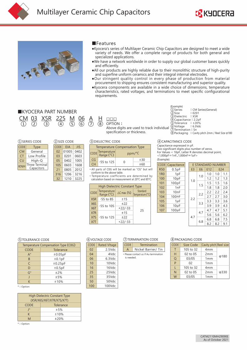
■Features●Kyocera's series of Multilayer Ceramic Chip Capacitors are designed to meet a wide
variety of needs. We offer a complete range of products for both general andspecialized applications.
●We have a network worldwide in order to supply our global customer bases quicklyand efficiently.
●All our products are highly reliable due to their monolithic structure of high-purityand superfine uniform ceramics and their integral internal electrodes.
●Our stringent quality control in every phase of production from materialprocurement to shipping ensures consistent manufacturing and superior quality.
●Kyocera components are available in a wide choice of dimensions, temperaturecharacteristics, rated voltages, and terminations to meet specific configurationalrequirements.
High Dielectric Constant Type
CODE TemperatureRange (℃)
△C max. (%)Standard
Temperature (℃)
X5R -55 to 85 ±15
25
X6S -55 to 105±22
X6T +22/-33X7R
-55 to 125±15
X7S ±22X7T +22/-33
③DIELECTRIC CODETemperature Compensation Type
CODE TemperatureRange (℃)
ppm/℃
CG -55 to 125 0±30
CH ±60・ All parts of C0G will be marked as “CG” but will
conform to the above table.・ Temperature coeff ic ients are determined by
calculation based on measurement at 20℃ and 85℃.
②SIZE CODECODE EIA JIS02 01005 040203 0201 060305 0402 1005105 0603 160821 0805 2012316 1206 321632 1210 3225
①SERIES CODECODE TypeCM GeneralCT Low ProfileCU High-Q
KNH Three TerminalCapacitors
⑤TOLERANCE CODETemperature Compensation Type (C0G)
CODE ToleranceA* ±0.05pFB ±0.1pFC ±0.25pFD ±0.5pFG* ±2%J ±5%K ±10%
* : Option
High Dielectric Constant Type (X5R/X6S/X6T/X7R/X7S/X7T)
CODE ToleranceJ* ±5%K ±10%M ±20%
* : Option
⑥VOLTAGE CODECODE Rated Vltage02 2.5Vdc04 4Vdc06 6.3Vdc10 10Vdc16 16Vdc25 25Vdc35 35Vdc50 50Vdc
100 100Vdc
⑦TERMINATION CODECODE Termination
A Nickel Barrier/ Tin・ Please contact us if Au termination
is needed.
⑧PACKAGING CODECODE Size Code Cavity pitch Reel size
T 105 to 32 4mm
φ180H 02 to 05 2mmQ 03/05 1mmP 02 1mmL 105 to 32 4mm
φ330N 02 to 05 2mmW 03/05 1mm
■KYOCERA PART NUMBERCM 03 X5R 225 M 06 A H □□□① ② ③ ④ ⑤ ⑥ ⑦ ⑧ OPTION :
Above digits are used to track individual specification or thickness.
(Example)①Series : CM Series(General)②Size : 0201③Dielectric : X5R④Capacitance : 2.2µF⑤Tolerance : ±20%⑥Voltage : 6.3Vdc⑦Termination : Sn⑧Packaging : Cavity pitch 2mm / Reel Size φ180
④CAPACITANCE CODECapacitance expressed in pF.Two significant digits plus number of zeros.For Values < 10pF, Letter R denotes decimal point,<1,000pF=1nF、1,000nF=1µF>(Example)
CODE CapacitanceR50 0.5pF1R0 1pF100 10pF101 100pF102 1nF103 10nF104 100nF105 1µF106 10µF107 100µF
E STANDARD NUMBERE3 E6 E12 E24
1.01.0 1.0 1.0 1.1
1.2 1.2 1.3
1.5 1.5 1.5 1.61.8 1.8 2.0
2.22.2 2.2 2.2 2.4
2.7 2.7 3.0
3.3 3.3 3.3 3.63.9 3.9 4.3
4.74.7 4.7 4.7 5.1
5.6 5.6 6.2
6.8 6.8 6.8 7.58.2 8.2 9.1
RoHS Compliant
CATM2110MH29090EAs of October 2021
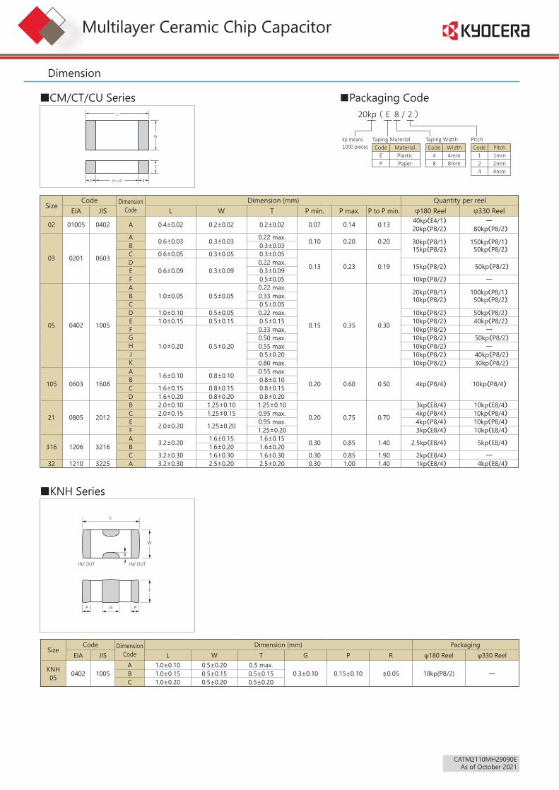
Multilayer Ceramic Chip Capacitor
■CM/CT/CU Series
�
T
L
P~P PP
■Packaging CodeE20kp 8 /
Taping Material Taping Width Pitch
2 )(
CodeEP
MaterialPlas�cPaper
kp means1000 pieces Code
48
Width4mm8mm
Code124
Pitch1mm2mm4mm
Dimension
SizeCode Dimension
CodeDimension (mm) Quantity per reel
EIA JIS L W T P min. P max. P to P min. φ180 Reel φ330 Reel
02 01005 0402 A 0.4±0.02 0.2±0.02 0.2±0.02 0.07 0.14 0.13 40kp(E4/1) ー
20kp(P8/2) 80kp(P8/2)
03 0201 0603
A 0.6±0.03 0.3±0.03 0.22 max. 0.10 0.20 0.20 30kp(P8/1)15kp(P8/2)
150kp(P8/1)50kp(P8/2)B 0.3±0.03
C 0.6±0.05 0.3±0.05 0.3±0.05
0.13 0.23 0.19D0.6±0.09 0.3±0.09
0.22 max. 15kp(P8/2) 50kp(P8/2)E 0.3±0.09F 0.5±0.05 10kp(P8/2) ー
05 0402 1005
A1.0±0.05 0.5±0.05
0.22 max.
0.15 0.35 0.30
20kp(P8/1)10kp(P8/2)
100kp(P8/1)50kp(P8/2)B 0.33 max.
C 0.5±0.05D 1.0±0.10 0.5±0.05 0.22 max. 10kp(P8/2) 50kp(P8/2)E 1.0±0.15 0.5±0.15 0.5±0.15 10kp(P8/2) 40kp(P8/2)F
1.0±0.20 0.5±0.20
0.33 max. 10kp(P8/2) ー
G 0.50 max. 10kp(P8/2) 50kp(P8/2)H 0.55 max. 10kp(P8/2) ー
J 0.5±0.20 10kp(P8/2) 40kp(P8/2)K 0.80 max. 10kp(P8/2) 30kp(P8/2)
105 0603 1608
A 1.6±0.10 0.8±0.10 0.55 max.
0.20 0.60 0.50 4kp(P8/4) 10kp(P8/4)B 0.8±0.10C 1.6±0.15 0.8±0.15 0.8±0.15D 1.6±0.20 0.8±0.20 0.8±0.20
21 0805 2012
B 2.0±0.10 1.25±0.10 1.25±0.10
0.20 0.75 0.70
3kp(E8/4) 10kp(E8/4)C 2.0±0.15 1.25±0.15 0.95 max. 4kp(P8/4) 10kp(P8/4)E 2.0±0.20 1.25±0.20 0.95 max. 4kp(P8/4) 10kp(P8/4)F 1.25±0.20 3kp(E8/4) 10kp(E8/4)
316 1206 3216A 3.2±0.20 1.6±0.15 1.6±0.15 0.30 0.85 1.40 2.5kp(E8/4) 5kp(E8/4)B 1.6±0.20 1.6±0.20C 3.2±0.30 1.6±0.30 1.6±0.30 0.30 0.85 1.90 2kp(E8/4) ー
32 1210 3225 A 3.2±0.30 2.5±0.20 2.5±0.20 0.30 1.00 1.40 1kp(E8/4) 4kp(E8/4)
■KNH Series
L
W
T
G
IN/ OUT IN/ OUT
R
P P
SizeCode Dimension
CodeDimension (mm) Packaging
EIA JIS L W T G P R φ180 Reel φ330 Reel
KNH05 0402 1005
A 1.0±0.10 0.5±0.20 0.5 max.0.3±0.10 0.15±0.10 ≧0.05 10kp(P8/2) ーB 1.0±0.15 0.5±0.15 0.5±0.15
C 1.0±0.20 0.5±0.20 0.5±0.20
CATM2110MH29090EAs of October 2021
CM Series
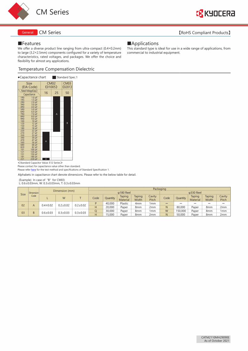
■FeaturesWe offer a diverse product line ranging from ultra-compact (0.4×0.2mm) to large (3.2×2.5mm) components configured for a variety of temperature characteristics, rated voltages, and packages. We offer the choice and flexibility for almost any applications.
■ApplicationsThis standard type is ideal for use in a wide range of applications, from commercial to industrial equipment.
CM Series 【RoHS Compliant Products】
Temperature Compensation Dielectric Part Number List : P21●Capacitance chart
Size (EIA Code)
CM02(01005)
CM03(0201)
Rated Voltage(Vdc) 16 25 50Capacitance1R0 1.0 pF 1R5 1.5 pF2R0 2.0 pF3R0 3.0 pF4R0 4.0 pF5R0 5.0 pF6R0 6.0 pF7R0 7.0 pF8R0 8.0 pF9R0 9.0 pF100 10 pF 120 12 pF150 15 pF180 18 pF220 22 pF
A
270 27 pF330 33 pF390 39 pF470 47 pF560 56 pF680 68 pF820 82 pF101 100 pF
B
121 120 pF151 150 pF181 180 pF221 220 pF
General
Size DimensionCode
Dimension (mm) Packagingφ180 Reel φ330 Reel
L W T Code Quantity Taping Material
Taping Width
Cavity Pitch Code Quantity Taping
MaterialTaping Width
Cavity Pitch
02 A 0.4±0.02 0.2±0.02 0.2±0.02 P 40,000 Plastic 4mm 1mm - - - - -
H 20,000 Paper 8mm 2mm N 80,000 Paper 8mm 2mm
03 B 0.6±0.03 0.3±0.03 0.3±0.03 Q 30,000 Paper 8mm 1mm W 150,000 Paper 8mm 1mmH 15,000 Paper 8mm 2mm N 50,000 Paper 8mm 2mm
(Example) In case of "B" for CM03;L: 0.6±0.03mm, W: 0.3±0.03mm, T: 0.3±0.03mm
Standard Spec.1
A
A
<Standard Capacitor Value: E12 Series>Please contact for capacitance value other than standard.Please refer here for the test method and specifications of Standard Specification 1.
Alphabets in capacitance chart denote dimensions. Please refer to the below table for detail.
CATM2110MH29090EAs of October 2021
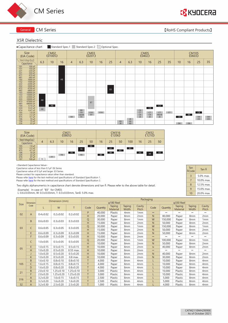
X5R Dielectric Part Number List : P22- 23●Capacitance chart
CM Series 【RoHS Compliant Products】General
Size (EIA Code)
CM02(01005)
CM03(0201)
CM05(0402)
CM105(0603)
Rated Voltage (Vdc) 6.3 10 16 4 6.3 10 16 25 4 6.3 10 16 25 35 10 16 25 35Capacitance101 100 pF 151 150 pF221 220 pF 331 330 pF 471 470 pF 681 680 pF102 1000 pF 152 1500 pF 222 2200 pF332 3300 pF472 4700 pF682 6800 pF 103 10000 pF
A8
B3
153 15000 pF 223 22000 pF333 33000 pF 473 47000 pF 683 68000 pF104 0.10 µF C3224 0.22 µF C8474 0.47 µF105 1.0 µF 225 2.2 µF 475 4.7 µF106 10 µF 156 15 µF226 22 µF
Size (EIA Code)
CM21(0805)
CM316(1206)
CM32(1210)
Rated Voltage(Vdc) 4 6.3 10 16 25 50 16 25 50 100 16 25 50Capacitance105 1.0 µF 225 2.2 µF 475 4.7 µF 106 10 µF B8 A3226 22 µF B8 A8476 47 µF107 100 µF
C8B8
C8
Size DimensionCode
Dimension (mm) Packagingφ180 Reel φ330 Reel
L W T Code Quantity Taping Material
Taping Width
Cavity Pitch Code Quantity Taping
MaterialTaping Width
Cavity Pitch
02 A 0.4±0.02 0.2±0.02 0.2±0.02 P 40,000 Plastic 4mm 1mm - - - - -
H 20,000 Paper 8mm 2mm N 80,000 Paper 8mm 2mm
03
B 0.6±0.03 0.3±0.03 0.3±0.03 Q 30,000 Paper 8mm 1mm W 150,000 Paper 8mm 1mmH 15,000 Paper 8mm 2mm N 50,000 Paper 8mm 2mm
C 0.6±0.05 0.3±0.05 0.3±0.05 Q 30,000 Paper 8mm 1mm W 150,000 Paper 8mm 1mmH 15,000 Paper 8mm 2mm N 50,000 Paper 8mm 2mm
E 0.6±0.09 0.3±0.09 0.3±0.09 H 15,000 Paper 8mm 2mm N 50,000 Paper 8mm 2mmF 0.6±0.09 0.3±0.09 0.5±0.05 H 10,000 Paper 8mm 2mm - - - - -
05
C 1.0±0.05 0.5±0.05 0.5±0.05 Q 20,000 Paper 8mm 1mm W 100,000 Paper 8mm 1mmH 10,000 Paper 8mm 2mm N 50,000 Paper 8mm 2mm
E 1.0±0.15 0.5±0.15 0.5±0.15 H 10,000 Paper 8mm 2mm n 40,000 Paper 8mm 2mmH 1.0±0.20 0.5±0.20 0.55 max. H 10,000 Paper 8mm 2mm - - - - -
J 1.0±0.20 0.5±0.20 0.5±0.20 H 10,000 Paper 8mm 2mm N 40,000 Paper 8mm 2mmK 1.0±0.20 0.5±0.20 0.8 max. H 10,000 Paper 8mm 2mm N 30,000 Paper 8mm 2mm
105B 1.6±0.10 0.8±0.10 0.8±0.10 T 4,000 Paper 8mm 4mm L 10,000 Paper 8mm 4mmC 1.6±0.15 0.8±0.15 0.8±0.15 T 4,000 Paper 8mm 4mm L 10,000 Paper 8mm 4mmD 1.6±0.20 0.8±0.20 0.8±0.20 T 4,000 Paper 8mm 4mm L 10,000 Paper 8mm 4mm
21 B 2.0±0.10 1.25±0.10 1.25±0.10 T 3,000 Plastic 8mm 4mm L 10,000 Plastic 8mm 4mmF 2.0±0.20 1.25±0.20 1.25±0.20 T 3,000 Plastic 8mm 4mm L 10,000 Plastic 8mm 4mm
316 A 3.2±0.20 1.6±0.15 1.6±0.15 T 2,500 Plastic 8mm 4mm L 5,000 Plastic 8mm 4mmB 3.2±0.20 1.6±0.20 1.6±0.20 T 2,500 Plastic 8mm 4mm L 5,000 Plastic 8mm 4mm
32 A 3.2±0.30 2.5±0.20 2.5±0.20 T 1,000 Plastic 8mm 4mm L 4,000 Plastic 8mm 4mm
A8
F8F8
B8
Tan δCode Tan δ
3 5.0% max.7 10.0% max.8 12.5% max.9 15.0% max.10 20.0% max.
Standard Spec.1 Optional Spec.Standard Spec.2
B3
A8A8
E8
B8C8
C8/E8 E9
B7
E10
E8J8
J8
C8
C8C7 C7
C8C7 C7
D8 D8D9 D9
CM Series
E10
A3
A3
F7F8
<Standard Capacitance Value>Cpacitance value of less than 0.1µF :E6 SeriesCpacitance value of 0.1µF and larger :E3 Series Please contact for capacitance value other than standard.Please refer here for the test method and specifications of Standard Specification 1.Please refer here for the test method and specifications of Standard Specification 2.
Two digits alphanumerics in capacitance chart denote dimensions and tan δ. Please refer to the above table for detail.(Example) In case of "B3" for CM03;L: 0.6±0.03mm, W: 0.3±0.03mm, T: 0.3±0.03mm, Tanδ: 5.0% max.
F9J8
K8E8
J8H8/J8
J8
D8 D8
F8
B3
F8
CATM2110MH29090EAs of October 2021
Size(EIA Code)
CM02(01005)
CM03(0201)
CM05(0402)
CM105(0603)
CM21(0805)
Rated Voltage(Vdc) 16 10 25 6.3 10 16 25 6.3 16 25 50Capacitance101 100 pF 151 150 pF221 220 pF 331 330 pF 471 470 pF 681 680 pF 102 1000 pF 152 1500 pF 222 2200 pF
A8
332 3300 pF 472 4700 pF 682 6800 pF 103 10000 pF
B3
153 15000 pF 223 22000 pF 333 33000 pF473 47000 pF 683 68000 pF104 0.10 µF C8224 0.22 µF 474 0.47 µF 105 1.0 µF B8 B8 B8225 2.2 µF C8 F8475 4.7 µF 106 10 µF F8
Size(EIA Code)
CM316(1206)
CM32(1210)
Rated Voltage(Vdc) 6.3 10 16 25 50 16 25 50Capacitance225 2.2 µF 475 4.7 µF 106 10 µF B8 A8 A3226 22 µF B8 A8
CM Series 【RoHS Compliant Products】
Tan δCode Tan δ
3 5.0% max.5 7.5% max.8 12.5% max.
X7R Dielectric Part Number List : P22-23●Capacitance chart
General
Size DimensionCode
Dimension (mm) Packagingφ180 Reel φ330 Reel
L W T Code Quantity Taping Material
Taping Width
Cavity Pitch Code Quantity Taping
MaterialTaping Width
Cavity Pitch
02 A 0.4±0.02 0.2±0.02 0.2±0.02 P 40,000 Plastic 4mm 1mm - - - - -
H 20,000 Paper 8mm 2mm N 80,000 Paper 8mm 2mm
03 B 0.6±0.03 0.3±0.03 0.3±0.03 Q 30,000 Paper 8mm 1mm W 150,000 Paper 8mm 1mmH 15,000 Paper 8mm 2mm N 50,000 Paper 8mm 2mm
05 C 1.0±0.05 0.5±0.05 0.5±0.05 Q 20,000 Paper 8mm 1mm W 100,000 Paper 8mm 1mmH 10,000 Paper 8mm 2mm N 50,000 Paper 8mm 2mm
105 B 1.6±0.10 0.8±0.10 0.8±0.10 T 4,000 Paper 8mm 4mm L 10,000 Paper 8mm 4mmC 1.6±0.15 0.8±0.15 0.8±0.15 T 4,000 Paper 8mm 4mm L 10,000 Paper 8mm 4mm
21 B 2.0±0.10 1.25±0.10 1.25±0.10 T 3,000 Plastic 8mm 4mm L 10,000 Plastic 8mm 4mmF 2.0±0.20 1.25±0.20 1.25±0.20 T 3,000 Plastic 8mm 4mm L 10,000 Plastic 8mm 4mm
316 B 3.2±0.20 1.6±0.20 1.6±0.20 T 2,500 Plastic 8mm 4mm L 5,000 Plastic 8mm 4mm32 A 3.2±0.30 2.5±0.20 2.5±0.20 T 1,000 Plastic 8mm 4mm L 4,000 Plastic 8mm 4mm
(Example) In case of "B3" for CM03;L: 0.6±0.03mm, W: 0.3±0.03mm, T: 0.3±0.03mm, Tanδ: 5.0% max.
Standard Spec.1
B5
X6S/X6T Dielectric Part Number List : P22-23●Capacitance chart
X6S X6TSize
(EIA Code)CM03(0201)
CM105(0603)
CM21(0805)
CM03(0201)
Rated Voltage(Vdc) 4 6.3 4 6.3 10 4 6.3 10 16 2.5Capacitance105 1.0 µF 225 2.2 µF475 4.7 µF106 10 µF226 22 µF 476 47 µF107 100 µF
(Example) In case of "D9" for CM105;L: 1.6±0.20mm, W: 0.8±0.20mm, T: 0.8±0.20mm, Tanδ: 15.0% max.
Size DimensionCode
Dimension (mm) Packagingφ180 Reel φ330 Reel
L W T Code Quantity Taping Material
Taping Width
Cavity Pitch Code Quantity Taping
MaterialTaping Width
Cavity Pitch
03 E 0.6±0.09 0.3±0.09 0.3±0.09 H 15,000 Paper 8mm 2mm N 50,000 Paper 8mm 2mm105 D 1.6±0.20 0.8±0.20 0.8±0.20 T 4,000 Paper 8mm 4mm L 10,000 Paper 8mm 4mm21 F 2.0±0.20 1.25±0.20 1.25±0.20 T 3,000 Plastic 8mm 4mm L 10,000 Plastic 8mm 4mm
Standard Spec.2
Tan δCode Tan δ
7 10.0% max.8 12.5% max.9 15.0% max.10 20.0% max.
F8
CM Series
F8
< Standard Capacitor Value : E3 Series >Please contact for capacitance value other than standard.Please refer here for the test method and specifications of Standard Specification 2.Two digits alphanumerics in capacitance chart denote dimensions and tan δ. Please refer to the above table for detail.
<Standard Capacitance Value>Capacitance value of less than 0.1µF: E6 Series / Capacitance value of 0.1µF and larger : E3 SeriesPlease contact for capacitance value other than standard.Please refer here for the test method and specifications of Standard Specification 1.Please refer here for the test method and specifications of Standard Specification 2.
Two digits alphanumerics in capacitance chart denote dimensions and tan δ. Please refer to the above table for detail.
F7
Standard Spec.2
E10 E10
D8 D8D9
F8
B3
F8
F3
B3B3
Optional Spec.
F8
E8
CATM2110MH29090EAs of October 2021
X7S X7TSize
(EIA Code)CM05(0402)
CM21(0805)
CM316(1206)
CM105(0603)
CM21(0805)
Rated Voltage(Vdc) 4 6.3 100 10 100 6.3 10 6.3Capacitance105 1.0 µF 225 2.2 µF D
475 4.7 µF 106 10 µF 226 22 µF
CM Series 【RoHS Compliant Products】
Two digits alphanumerics in capacitance chart denote dimensions and tan δ. Please refer to the above table for detail.
Tan δCode Tan δ
3 5.0% max.5 7.5% max.8 12.5% max.9 15.0% max.
X7S/X7T Dielectric Part Number List : P22-23●Capacitance chart
General
Size DimensionCode
Dimension (mm) Packagingφ180 Reel φ330 Reel
L W T Code Quantity Taping Material
Taping Width
Cavity Pitch Code Quantity Taping
MaterialTaping Width
Cavity Pitch
05 C 1.0±0.05 0.5±0.05 0.5±0.05 H 10,000 Paper 8mm 2mm N 50,000 Paper 8mm 2mmE 1.0±0.15 0.5±0.15 0.5±0.15 H 10,000 Paper 8mm 2mm N 40,000 Paper 8mm 2mm
105 D 1.6±0.20 0.8±0.20 0.8±0.20 T 4,000 Paper 8mm 4mm L 10,000 Paper 8mm 4mm21 F 2.0±0.20 1.25±0.20 1.25±0.20 T 3,000 Plastic 8mm 4mm L 10,000 Plastic 8mm 4mm
316 B 3.2±0.20 1.6±0.20 1.6±0.20 T 2,500 Plastic 8mm 4mm L 5,000 Plastic 8mm 4mmC 3.2±0.30 1.6±0.30 1.6±0.30 T 2,000 Plastic 8mm 4mm - - - - -
(Example) In case of "D9" for CM105;L: 1.6±0.20mm, W: 0.8±0.20mm, T: 0.8±0.20mm, Tanδ: 15.0% max.
Standard Spec.1 Standard Spec.2
B5 F8
CM Series
Please refer here for the test method and specifications of Standard Specification 1. Please refer here for the test method and specifications of Standard Specification 2.
D8D9
C3B3
F3C8C8E3
CATM2110MH29090EAs of October 2021
Multilayer Ceramic Chip Capacitors
Test Conditions and Specifications for Temperature Compensation Type (CΔ Characteristics)CM / CU Series (Standard Spec.1)
Test Items Test Conditions Specifications
Capacitance Value (C) Capacitance Frequency VoltC≤1000pF 1MHz±10% 0.5 to 5VrmsC>1000pF 1kHz±10%
Within tolerance
Q C≥30pF : Q≥1000C<30pF : Q≥400+20C
Insulation Resistance (IR)Apply the rated voltage for 1minute, and measure it in nor-mal temperature and humidity.The charge and discharge current of the capacitor must not exceed 50mA.
Over 10000MΩ or 500MΩ・µF, whichever is less
Dielectric ResistanceApply*3 times of the rated voltage for 1 to 5 seconds.*CU02C△R20-120/25V: twiceThe charge and discharge current of the capacitor must not exceed 50mA.
No problem observed
Appearance Microscope No problem observed
Termination StrengthApply a sideward force of 500g (5N) to a PCB-mounted sample. note: 2N for 0201 size, and 1N for 01005 size.
No problem observed
Bending Strength Glass epoxy PCB: Fulcrum spacing: 90mm, duration time 10 seconds. No significant damage with 1mm bending.
Vibration Test Appearance Vibration frequency: 10 to 55 (Hz)Amplitude: 1.5mmSweeping condition: 10→55→10Hz/ 1 minute in X, Y and Z directions: 2 hours each, 6 hours in total.
No problem observed
ΔC Within Tolerance
Q C≥30pF : Q≥1000C<30pF : Q≥400+20C
Soldering HeatResistant
Appearance Soak the sample in 260℃±5℃ solder for 10±0.5 seconds and place in normal temperature and humidity, and measure the sample after 24±2 hours.(Pre-heating conditions)
Order Temperature Time1 80 to 100℃ 2 minutes2 150 to 200℃ 2 minutes
The charge and discharge current of the capacitor must not exceed 50mA for IR and withstanding voltage measurement.
No problem observed
ΔC Within±2.5% or±0.25pF, whichever is larger
Q C≥30pF : Q≥1000C<30pF : Q≥400+20C
IR Over 10000MΩ or 500MΩ・µF whichever is less
Withstanding Voltage Resist without problem
SolderablitySoaking condition
Sn-3Ag-0.5Cu 245±5℃ 3±0.5 sec.Sn63 Solder 235±5℃ 2±0.5 sec.
Solder coverage : 95% min.
TemperatureCycle
Appearance(Cycle)Room temperature (3 min.)→Lowest operation temperature (30 min.)→Room temperature (3 min.)→Highest operation temperature(30 min.)After 5 cycles, measure after 24±2 hours.The charge and discharge current of the capacitor must not exceed 50mA for IR and withstanding voltage measurement.
No problem observed
ΔC Within±2.5% or ±0.25pF, whichever is larger
Q C≥30pF : Q≥1000C<30pF : Q≥400+20C
IR Over 10000MΩ or 500MΩ・µF, whichever is less
Withstanding Voltage Resist without problem
Moisture Resistant Load
Appearance After applying the rated voltage for 500+12/ −0 hours in the condition of 40℃±2℃ and 90 to 95%RH, allow the parts to stabilize in normal temperature and humidity for 24±2 hours, before measurement.The charge and discharge current of the capacitor must not exceed 50mA for IR measurement.
No problem observed
ΔC Within±7.5% or ±0.75pF, whichever is larger
Q C≥30pF : Q≥200C<30pF : Q≥100+10C/ 3
IR Over 500MΩ or 25MΩ・µF, whichever is less
High- Temperature Load
Appearance After applying *twice the rated voltage in the temperature of 125±3℃ for 1000+12/ −0 hours, measure the sample after 24±2 hours in normal temperature and humidity. The charge and discharge current of the capacitor must not exceed 50mA for IR measurement.*Applied voltages for respective products are indicated in the chart below.
No problem observed.
ΔC Within ±3% or ±0.3pF, whichever is larger
QC≥30pF : Q≥35010pF<C<30pF : Q≥275+5C/ 2C<10pF : Q≥200+10C
IR Over 1000MΩ or 50MΩ・µF, whichever is less
Please ask for individual specification for the hatched range in previous chart.Voltage to be applied in the High Temperature Load (Applied voltage is the multiple of the rated volatage)
Applied Voltage Rated Voltage Products×1.0 16V CM02CΔ221×1.2 25V CM02CΔR20-120
Test Conditions and Standards
CATM2110MH29090EAs of October 2021
Test Conditions and Specifications for High Dielectric Type (X5R, X7R, X7S)CM / CT Series (Standard Spec.1)
Test Items Test Conditions Specifications
Capacitance Value (C) Measure after heat treatmentCapacitance Frequency Volt
C≤10µF 1kHz±10% 1.0±0.2Vrms*1kHz±10% 0.5±0.2Vrms
C>10µF 120Hz±10% 0.5±0.2Vrms*CM02X5R104□06A#The charge and discharge current of the capacitor must not exceed 50mA.
Within tolerance
Tanδ Refer to capacitance chart
Insulation Resistance (IR)Apply the rated voltage for 1 minute, and measure it in nor-mal temperature and humidity.The charge and discharge current of the capacitor must not exceed 50mA.
Over 10000MΩ or 500MΩ・µF, whichever is less
Dielectric ResistanceApply *2.5 times of the rated voltage for 1 to 5 seconds.*CM316X5R225, CM316X7S225/100V: twiceThe charge and discharge current of the capacitor must not exceed 50mA.
No problem observed
Appearance Microscope No problem observed
Termination StrengthApply a sideward force of 500g (5N) to a PCB-mounted sample. note : 2N for 0201 size, and 1N for 01005 size.Exclude CT series with thickness of less than 0.66mm.
No problem observed
Bending StrengthGlass epoxy PCB: Fulcrum spacing: 90mm, duration time 10 seconds.Exclude CT series with thickness of less than 0.66mm.
No significant damage with 1mm bending
VibrationTest Appearance Take the initial value after heat treatment.
Vibration frequency: 10 to 55 (Hz)Amplitude: 1.5mmSweeping condition: 10→55→10Hz/ 1 minute in X, Y and Z direc-tions: 2 hours each, 6 hours in total, and place in normal tempera-ture and humidity, then measure the sample after heat treatment.
No problem observed
ΔC Within tolerance
Tanδ Within tolerance
Soldering HeatResistant
Appearance Take the initial value after heat treatment.Soak the sample in 260℃±5℃ solder for 10±0.5 seconds and place in normal temperature and humidity, and measure after heat treatment.(Pre-heating conditions)
Order Temperature Time1 80 to 100℃ 2 minutes2 150 to 200℃ 2 minutes
The charge and discharge current of the capacitor must not exceed 50mA for IR and withstanding voltage measurement.
No problem observed
ΔC Within±7.5%
Tanδ Within tolerance
IR Over 10000MΩ or 500MΩ・µF, whichever is less
Withstanding Voltage Resist without problem
SolderablitySoaking condition
Sn-3Ag-0.5Cu 245±5℃ 3±0.5 sec.Sn63 Solder 235±5℃ 2±0.5 sec.
Solder coverage : 95% min.
TemperatureCycle
Appearance Take the initial value after heat treatment.(Cycle)Room temperature (3 min.)→Lowest operation temperature (30 min.)→Room temperature (3 min.)→Highest operation temperature(30 min.)After 5 cycles, measure after heat treatment.The charge and discharge current of the capacitor must not exceed 50mA for IR and withstanding voltage measurement.
No problem observedΔC Within±7.5%Tanδ Within toleranceIR Over 10000MΩ or 500MΩ・µF, whichever is less
Withstanding Voltage Resist without problem
Moisture Resistant Load
Appearance Take the initial value after heat treatment.After applying rated voltage for 500+12/ −0 hours in the condi-tion of 40℃±2℃ and 90 to 95%RH, and place in normal tempera-ture and humidity, then measure the sample after heat treatment.The charge and discharge current of the capacitor must not exceed 50mA for IR measurement.
No problem observedΔC Within±12.5%
Tanδ 200% max. of initial value
IR Over 500MΩ or 25MΩ・µF, whichever is lessHigh-TemperatureLoad
Appearance Take the initial value after heat treatment.After applying *twice the rated voltage at the highest operation temperature for 1000+12/ −0 hours, and measure the sample after heat treatment in normal temperature and humidity.The charge and discharge current of the capacitor must not exceed 50mA for IR measurement.*Apply 1.5 times when the rated voltage is 10V or less. Applied voltages for respective products are indicated in the chart below.
No problem observed
ΔC Within±12.5%
Tanδ 200% max. of initial value
IR Over 1000MΩ or 50MΩ・µF, whichever is less
Heat treatment Expose sample in the temperature of 150+0/ −10℃ for 1 hour and leave the sample in normal temperature andhumidity for 24±2 hours.
Voltage to be applied in the High Temperature Load (Applied voltage is the multiple of the rated voltage)Applied Voltage Rated Voltage Products
×1.0 10V CM02X5R104100V CM316X5R225, CM316X7S225
×1.3 6.3V CM02X5R153-104, CT03X5R104
×1.5
16V CM02X5R101-103, CM05X5R224, CM105X5R225, CM21X5R106, CM316X5R226, CM02X7R101-222, CM105X7R105, CM316X7R106, CM32X7R226, CT105X5R105, CT21X5R475
25V CM03X5R332-103, CM105X5R105, CM21X5R225-475, CM316X5R106, CM32X5R106-226, CM05X7R104, CM21X7R105-225, CM316X7R475, CM32X7R106
50V CM21X5R105, CM316X5R475, CM32X5R106, CM21X7R105, CM32X7R106, CT21X5R225, Please contact us for the optional specifications of the capacitance chart.
Test Conditions and Standards
Multilayer Ceramic Chip Capacitors
12 CATM2110MH29090E
As of October 2021
Test Conditions and Specifications for High Dielectric Type (X5R, X6S, X7R, X7S, X7T)CM / CT Series (Standard Spec.2)
Test Items Test Conditions Specifications
Capacitance Value (C) Measure after heat treatmentCapacitance Frequency Volt
C≤10µF 1kHz±10% 1.0±0.2Vrms*1kHz±10% 0.5±0.2Vrms
C>10µF 120Hz±10% 0.5±0.2Vrms*CM02X5R474M06A#, CM03X5R225□06A#, CM03X5R225M06A#035, CM03X5R475M06A#055, CM03X5R475M04A#, CM05X5R106M06A#, CT05X5R475M06A#033 The charge and discharge current of the capacitor must not exceed 50mA.
Within tolerance
Tanδ Refer to capacitance chart
Insulation Resistance (IR)Apply the rated voltage for 1minute, and measure it in nor-mal temperature and humidity.The charge and discharge current of the capacitor must not exceed 50mA.
Over 50MΩ・µF
Dielectric ResistanceApply *2.5 times of the rated voltage for 1 to 5 seconds.*CM21X7S105, CM316X7S475/100V: twiceThe charge and discharge current of the capacitor must not exceed 50mA.
No problem observed
Appearance Microscope No problem observed
Termination StrengthApply a sideward force of 500g (5N) to a PCB-mounted sample. note : 2N for 0201 size, and 1N for 01005 size.Exclude CT series with thickness of less than 0.66mm.
No problem observed
Bending Strength Glass epoxy PCB: Fulcrum spacing: 90mm, duration time 10 seconds.Exclude CT series with thickness of less than 0.66mm. No significant damage with 1mm bending
VibrationTest Appearance Take the initial value after heat treatment.
Vibration frequency: 10 to 55 (Hz)Amplitude: 1.5mmSweeping condition: 10→55→10Hz/ 1 minute in X, Y and Z direc-tions: 2 hours each, 6 hours in total, and place in normal tempera-ture and humidity, then measure the sample after heat treatment.
No problem observed
ΔC Within tolerance
Tanδ Within tolerance
Soldering HeatResistant
Appearance Take the initial value after heat treatment.Soak the sample in 260℃±5℃ solder for 10±0.5 seconds and place in normal temperature and humidity, and measure after heat treatment.(Pre-heating conditions)
Order Temperature Time1 80 to 100℃ 2 minutes2 150 to 200℃ 2 minutes
The charge and discharge current of the capacitor must not exceed 50mA for IR and withstanding voltage measurement.
No problem observed
ΔC Within±7.5%
Tanδ Within tolerance
IR Over 50MΩ・µF
Withstanding Voltage Resist without problem
SolderablitySoaking condition
Sn-3Ag-0.5Cu 245±5℃ 3±0.5 sec.Sn63 Solder 235±5℃ 2±0.5 sec.
Solder coverage : 95% min.
TemperatureCycle
Appearance Take the initial value after heat treatment.(Cycle)Room temperature (3 min.)→Lowest operation temperature (30 min.)→Room temperature (3 min.)→Highest operation temperature(30 min.)After 5 cycles, measure after heat treatment.The charge and discharge current of the capacitor must not exceed 50mA for IR and withstanding voltage measurement.
No problem observedΔC Within±7.5%Tanδ Within toleranceIR Over 50MΩ・µFWithstanding Voltage Resist without problem
Moisture Resistant Load
Appearance Take the initial value after heat treatment.After applying rated voltage for 500+12/ −0 hours in the condi-tion of 40℃±2℃ and 90 to 95%RH, and place in normal tempera-ture and humidity, then measure the sample after heat treatment.The charge and discharge current of the capacitor must not exceed 50mA for IR measurement.
No problem observedΔC Within±12.5%
Tanδ 200% max. of initial value
IR Over 10MΩ・µFHigh-TemperatureLoad
Appearance Take the initial value after heat treatment.After applying *□ times the rated voltage at the highest operation temperature for 1000+12/ −0 hours, and measure the sample after heat treatment in normal temperature and humidity.The charge and discharge current of the capacitor must not exceed 50mA for IR measurement.*Apply 1.0 times when the rated voltage is 4V or less. Applied volt-ages for respective products are indicated in the chart below.
No problem observed
ΔC Within±12.5%
Tanδ 200% max. of initial value
IR Over 10MΩ・µF
Heat treatment Expose sample in the temperature of 150+0/ −10℃ for 1 hour and leave the sample in normal temperature andhumidity for 24±2 hours.
Voltage to be applied in the High Temperature Load (Applied voltage is the multiple of the rated voltage)Applied Voltage
Rated Voltage Products Applied
VoltageRated
Voltage Products
×1.0
6.3VCM02X5R224, CM02X5R474, CM03X5R225, CM03X5R475, CM05X5R106 ×1.2 6.3V CM03X5R105 CM05X5R156, CM05X5R226, CM21X5R476, CM03X6S105, CM105X6S226
×1.36.3V CM03X5R474
CT05X5R105, CT05X5R225, CT05X5R475 10V CM03X5R223-224, CM05X5R105-22510V CM03X5R225, CM105X5R226, CM21X6S226 16V CM05X5R105
16V CM03X5R105, CM05X5R225, CM05X5R475, CM105X5R226
×1.5
6.3V CM21X6S226, CM05X7S105CM21X6S226, CM21X7R475 CM105X7T106, CM21X7T226
25VCM05X5R105, CM05X5R225, CM05X5R475,CM105X5R475
10VCM05X5R474, CM05X5R475, CM21X5R226
CM105X5R106, CM21X5R226 CM105X6S106, CM105X7T47535V CM05X5R105, CM105X5R475, CM105X5R106 25V CM105X7R105, CM316X7R106
100V CM21X7S105, CM316X7S475 50V CM316X7R475Please contact us for the optional specifications of the capacitance chart.
Test Conditions and Standards
Multilayer Ceramic Chip Capacitors
CATM2110MH29090EAs of October 2021
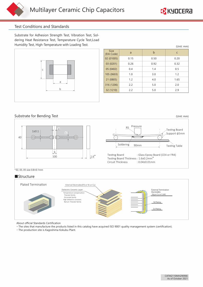
Substrate for Adhesion Strength Test, Vibration Test, Sol-dering Heat Resistance Test, Temperature Cycle Test,Load Humidity Test, High-Temperature with Loading Test. (Unit: mm)
Size(EIA Code) a b c
02 (01005) 0.15 0.50 0.20
03 (0201) 0.26 0.92 0.32
05 (0402) 0.4 1.4 0.5
105 (0603) 1.0 3.0 1.2
21 (0805) 1.2 4.0 1.65
316 (1206) 2.2 5.0 2.0
32 (1210) 2.2 5.0 2.9
40
b100
1±0.1
1.6*
ac
90mm
R5
Soldering
Support φ5mmTes�ng Board
Tes�ng Table
Tes�ng Board : Glass Epoxy Board (CE4 or FR4)Tes�ng Board Thickness : 1.6±0.2mm*Circuit Thickness : 0.04±0.01mm
Pressure
a
b
c
Substrate for Bending Test (Unit: mm)
* 02, 03, 05 size 0.8±0.1mm
Test Conditions and Standards
Multilayer Ceramic Chip Capacitors
■Structure
Internal Electrodes(Pd or Ni or Cu)
Dielectric Ceramic LayerTemperature compensa�on: Titanate family Zirconate familyHigh dielectric constant: Barium Titanate family
External Termination Electrodes(Ag or Cu or CuNi)
Ni Plating
Sn Plating
Plated Termina�on
About official Standards Certification・The sites that manufacture the products listed in this catalog have acquired ISO 9001 quality management system (certification).・The production site is Kagoshima Kokubu Plant.
CATM2110MH29090EAs of October 2021
H GF
A
B
(Paper)(Plas�c)
0.6 max. 1.2 max.
2.8 max.
C
E
D
Feed HolePunched rectangular holeto hold capacitorJ
Holes only for plas�c carrier tape. f 0.3 min.
F=4mm (105, 21, 316, 32 Size)
Feed HolePunched rectangular holeto hold capacitorJ
F H
(Paper)
F
A
B C
E
D
02 Size: 0.4 max. 03 Size: 0.6 max. *1)Applicable to product thickness of 0.5±0.05 05 Size: 0.8 max.
*2)Applicable to product thickness of 0.8max.
0.8 max.*1)
1.0 max.*2)
F=2mm (02, 03, 05 Size)
HFF
AB
C
E
D
Feed Hole Parts inser�on cavityJ (Paper)
02 Size: 0.4 max.03 Size: 0.5 max.05 Size: 0.75 max.
F=1mm (02, 03, 05 Size)
(Plas�c)
0.5 max.HF
A
BC
E
D
Feed HolePunched rectangularhole to holdJ
F=1mm (02 Size)
A
R
EC
D
W1
W2
B
Reel
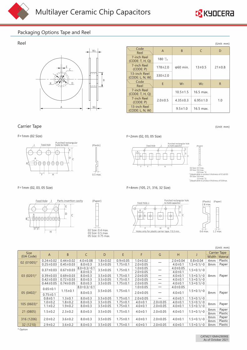
Carrier Tape (Unit: mm)
(Unit: mm)
Code A B C DReel7-inch Reel
(CODE: T, H, Q) 180 +0 −2.0
φ60 min. 13±0.5 21±0.87-inch Reel(CODE: P) 178±2.0
13-inch Reel(CODE: L, N, W) 330±2.0
Code E W1 W2 RReel7-inch Reel
(CODE: T, H, Q)
2.0±0.5
10.5±1.5 16.5 max.
1.07-inch Reel(CODE: P) 4.35±0.3 6.95±1.0
13-inch Reel(CODE: L, N, W) 9.5±1.0 16.5 max.
(Unit: mm)
Size(EIA Code) A B C D E F G H J Carrier Tape
Width Material02 (01005)* 0.24±0.02 0.44±0.02 4.0±0.08 1.8±0.02 0.9±0.05 1.0±0.02
ー2.0±0.04 0.8±0.04 4mm Plastic
0.25±0.03 0.45±0.03 8.0±0.3 3.5±0.05 1.75±0.1 2.0±0.05 4.0±0.1 1.5+0.1/-0 8mm Paper
03 (0201)*0.37±0.03 0.67±0.03 8.0+0.3/-0.1 3.5±0.05 1.75±0.1 1.0±0.05
ー4.0±0.05 1.5+0.1/-0
8mm Paper8.0±0.3 2.0±0.05 4.0±0.1
0.39±0.03 0.69±0.03 8.0±0.3 3.5±0.05 1.75±0.1 2.0±0.05 ー 4.0±0.1 1.5+0.1/-00.42±0.03 0.72±0.03 8.0±0.3 3.5±0.05 1.75±0.1 2.0±0.05 ー 4.0±0.1 1.5+0.1/-00.44±0.05 0.74±0.05 8.0±0.3 3.5±0.05 1.75±0.1 2.0±0.05 ー 4.0±0.1 1.5+0.1/-0
05 (0402)*0.65±0.1 1.15±0.1
8.0+0.3/-0.13.5±0.05 1.75±0.1
1.0±0.05 ー 4.0±0.051.5+0.1/-0 8mm Paper8.0±0.3 2.0±0.05 ー 4.0±0.10.75±0.1
0.8±0.1 1.3±0.1 8.0±0.3 3.5±0.05 1.75±0.1 2.0±0.05 ー 4.0±0.1 1.5+0.1/-0105 (0603)* 1.0±0.2 1.8±0.2 8.0±0.3 3.5±0.05 1.75±0.1 4.0±0.1 2.0±0.05 4.0±0.1 1.5+0.1/-0 8mm Paper1.1±0.2 1.9±0.2 8.0±0.3 3.5±0.05 1.75±0.1 4.0±0.1 2.0±0.05 4.0±0.1 1.5+0.1/-021 (0805) 1.5±0.2 2.3±0.2 8.0±0.3 3.5±0.05 1.75±0.1 4.0±0.1 2.0±0.05 4.0±0.1 1.5+0.1/-0 8mm Paper
8mm Plastic
316 (1206) 2.0±0.2 3.6±0.2 8.0±0.3 3.5±0.05 1.75±0.1 4.0±0.1 2.0±0.05 4.0±0.1 1.5+0.1/-0 8mm Paper8mm Plastic
32 (1210) 2.9±0.2 3.6±0.2 8.0±0.3 3.5±0.05 1.75±0.1 4.0±0.1 2.0±0.05 4.0±0.1 1.5+0.1/-0 8mm Plastic* Option
Packaging Options Tape and Reel
Multilayer Ceramic Chip Capacitors
CATM2110MH29090EAs of October 2021
Packaging Options
Multilayer Ceramic Chip Capacitors
Carrier Tape
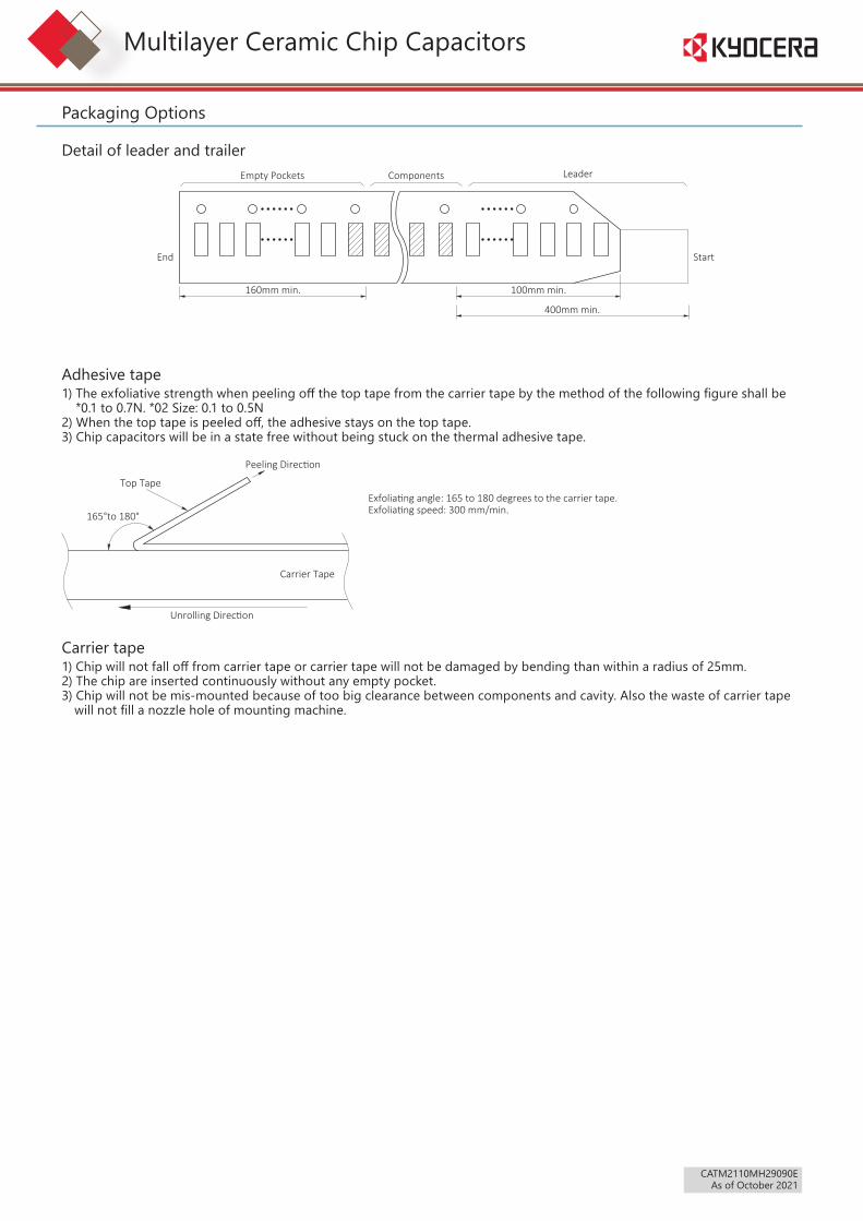
Peeling Direc�on
Unrolling Direc�on
165°to 180°
Top TapeExfolia�ng angle: 165 to 180 degrees to the carrier tape.Exfolia�ng speed: 300 mm/min.
Adhesive tape1) The exfoliative strength when peeling off the top tape from the carrier tape by the method of the following figure shall be
*0.1 to 0.7N. *02 Size: 0.1 to 0.5N2) When the top tape is peeled off, the adhesive stays on the top tape.3) Chip capacitors will be in a state free without being stuck on the thermal adhesive tape.
Carrier tape1) Chip will not fall off from carrier tape or carrier tape will not be damaged by bending than within a radius of 25mm.2) The chip are inserted continuously without any empty pocket.3) Chip will not be mis-mounted because of too big clearance between components and cavity. Also the waste of carrier tape
will not fill a nozzle hole of mounting machine.
Detail of leader and trailer
160mm min. 100mm min.
400mm min.
Empty Pockets Components
StartEnd
Leader
CATM2110MH29090EAs of October 2021
Surface Mounting Information
Multilayer Ceramic Chip Capacitors
Dimensions for recommended typical landSince the amount of solder (size of fillet) to be used has direct influence on the capacitor after mounting, the sufficient consideration is necessary.When the amounts of solder is too much, the stress that a capacitor receives becomes larger. It may become the cause of a crack in the capacitor. When the land design of printed wiring board is considered, it is necessary to set up the form and size of land pattern so that the amount of solder is suitable.
Design of printed circuit and SolderingThe recommended fillet height shall be 1/2 of the thickness of capacitors or 0.5mm. When mounting two or more capacitors in the common land, it is necessary to separate the land with the solder resist strike so that it may become the exclusive land of each capacitor.
Ideal Solder Height
Chip Capacitor
PCB
Solder
T/ 2 or 0.5mm
T
Item Prohibited Recommended example : Separation by solder resist
Multiple parts mount
Solder resist
Mount withleaded parts
Leaded parts Leaded parts
Solder resist
Wire soldering after mounting
Soldering iron
WireSolder resist
Side by side layout
Solder resist Solder resist
(General)
Land Pa�ernSample capacitor
Soldering resist
b a
c
General (Unit: mm)
Size(EIA Code)
Dimension Recommended land dimensions
L W a b c
02 (01005) 0.4±0.02 0.2±0.02 0.13 to 0.20 0.12 to 0.18 0.20 to 0.23
03 (0201)0.6±0.03 0.3±0.03
0.20 to 0.25 0.25 to 0.35 0.30 to 0.400.6±0.05 0.3±0.050.6±0.09 0.3±0.09 0.23 to 0.30 0.25 to 0.35 0.30 to 0.45
05 (0402)1.0±0.05 0.5±0.05 0.30 to 0.50 0.35 to 0.45 0.40 to 0.601.0±0.15 0.5±0.15
0.40 to 0.60 0.40 to 0.50 0.50 to 0.751.0±0.20 0.5±0.20
105 (0603)
1.6±0.10 0.8±0.10 0.70 to 1.00 0.80 to 1.00 0.60 to 0.901.6±0.15 0.8±0.15
0.80 to 1.00 0.80 to 1.00 0.80 to 1.101.6±0.20 0.8±0.201.6±0.25 0.8±0.25
21 (0805)2.0±0.10 1.25±0.10 1.00 to 1.30 1.00 to 1.20 1.00 to 1.452.0±0.15 1.25±0.15
1.00 to 1.30 1.00 to 1.20 1.25 to 1.552.0±0.20 1.25±0.20
316 (1206)3.2±0.20 1.6±0.15 2.10 to 2.50 1.10 to 1.30 1.40 to 1.903.2±0.20 1.6±0.20
2.10 to 2.50 1.10 to 1.30 1.60 to 2.003.2±0.30 1.6±0.30
32 (1210) 3.2±0.30 2.5±0.20 2.10 to 2.50 1.10 to 1.30 1.90 to 2.80* Recommended land dimensions may differ depending on dimensional tolerance.
CATM2110MH29090EAs of October 2021
Surface Mounting Information
Multilayer Ceramic Chip Capacitors
Mounting DesignThe chip could crack if the PCB warps during processing after the chip has been soldered.
(Not recommended) (Ideal)
Crack
Support pin
(Not recommended) (Ideal)
Recommended chip position on PCB to minimize stress from PCB warpage
Actual Mounting1) If the position of the vacuum nozzle is too low, a large force may be applied to the chip capacitor during mounting,
resulting in cracking.2) During mounting, set the nozzle pressure to a static load of 1 to 3 N.3) To minimize the shock of the vaccum nozzle, provide a support pin on the back of the PCB to minimize PCB
flexture.
4) Bottom position of pick up nozzle should be adjusted to the top surface of a substrate which camber is corrected.
Resin Mold1) If a large amount of resin is used for molding the chip, cracks may occur due to contraction stress during curing.
To avoid such cracks, use a low shrinkage resin.2) The insulation resistance of the chip will degrade due to moisture absorption. Use a low moisture absorption
resin.3) Check carefully that the resin does not generate a decomposition gas or reaction gas during the curing process
or during normal storage. Such gases may crack the chip capacitor or damage the device itself.
CATM2110MH29090EAs of October 2021
Surface Mounting Information
Multilayer Ceramic Chip Capacitors
Soldering Method1) Ceramic is easily damaged by rapid heating or cooling. If some heat shock is unavoidable, preheat enough to limit the
temperature difference (Delta T) to within 150 degree Celsius.2) The product size 1.6×0.8mm to 3.2×1.6mm can be used in reflow and wave soldering, and the product size of bigger than
3.2×1.6mm, or smaller than 1.6×0.8mm can be used in reflow. Circuit shortage and smoking can be created by using capacitors which are used neglecting the above caution.
3) Please see our recommended soldering conditions.4) In case of using Sn-Zn Solder, please contact us in advance.5) The following condition is recommended for spot heater application.
・ Recommended spot heater conditionItem Condition
Distance 5mm min.
Angle 45°
Projection Temp. 400℃ max.
Flow rate Set at the minimum
Nozzle diameter 2φ to 4φ (Single hole type)
Application time 10 sec. max. (1206 and smaller)30 sec. max. (1210 and larger)
How to point spot heater
Single hole nozzle
Angle 45°
Recommended Temperature Profile (63Sn Solder)
Reflow
∆T
300
250
200
150
100
50
0
Preheat
60 sec.
Peak temperature230℃±5℃15 sec. max.
60 sec.
More than180℃, 40 sec. max.
Cool at normal room temperature
① Minimize soldering �me.② Ensure that the temperature difference (∆T) does not exceed 150℃.③ Ensure that the temperature difference (∆T) does not exceed 130℃ for 3.2×2.5mm size or larger.④ MLCC can withstand the above reflow conditions up to 3 times.
Tem
pera
ture
(
)℃
Wave
① Ensure that the chip capacitor is preheated adequately.② Ensure that the temperature difference (∆T) does not exceed 150℃.③ Cool naturally a�er soldering.④ Wave soldering is not applicable for chips with size of 3.2×2.5mm or larger of 1.0×0.5mm or smaller and capacitor arrays.
300
250
200
150
100
50
0
Preheat
Tem
pera
ture
(
)
60 to 120 sec. 5 sec. max.
Cool at normalroom temperature
Peak Temperature230℃ to 260℃
∆T
℃
Recommended Temperature Profile (Sn-3Ag-0.5Cu)
Reflow
300
250
200
150
100
50
0
Preheat
Peak temperature250℃±10℃5 to 10 sec. max.
90±30 sec.
More than 220℃90 sec. max.
170 to 180℃1 to 3℃/ sec.
① Minimize soldering �me.② Ensure that allowable temperature difference does not exceed 150℃.③ Ensure that allowable temperature difference does not exceed 130℃ for 3.2×2.5mm size or larger.④ MLCC can withstand the above reflow conditions up to 3 times.⑤ N₂ atmosphere is recommended for reflow of products of 0.4mm×0.2mm size or smaller.
Cool at normalroom temperature
Tem
pera
ture
(
)℃ ∆T
Wave
① Ensure that the chip capacitor is preheated adequately.② Ensure that the temperature difference (∆T) does not exceed 150℃.③ Cool naturally a�er soldering.④ Wave soldering is not applicable for chips with size of 3.2×2.5mm or larger of 1.0×0.5mm or smaller and capacitor arrays.
Preheat300
250
200
150
100
50
Tem
pera
ture
(
)
0
Cool at normalroom temperature
Peak Temperature245℃ to 260℃
∆T
60 to 120 sec. 5 sec. max.
℃
CATM2110MH29090EAs of October 2021
Precautions
Multilayer Ceramic Chip Capacitors
Circuit Design1. Once application and assembly environments have been checked, the capacitor may be used in conformance
with the rating and performance which are provided in both the catalog and the specifications. Use exceeding that which is specified may result in inferior performance or cause a short, open, smoking, or flaming to occur, etc.
2. Please consult the manufacturer in advance when the capacitor is used in devices such as: devices which dealwith human life, i.e. medical devices; devices which are highly public orientated; and devices which demand a high standard of liability.Accident or malfunction of devices such as medical devices, space equipment and devices having to do withatomic power could generate grave consequence with respect to human lives or, possibly, a portion of the public. Capacitors used in these devices may require high reliability design different from that of general purposecapacitors.
3. Please use the capacitors in conformance with the operating temperature provided in both the catalog and thespecifications.Be especially cautious not to exceed the maximum temperature. In the situation the maximum temperature set forthin both the catalog and specifications is exceeded, the capacitor's insulation resistance may deteriorate, power may suddenly surge and short-circuit may occur.The capacitor has a loss, and may self-heat due to equivalent series resistance when alternating electric currentis passed therethrough. As this effect becomes especially pronounced in high frequency circuits, please exercisecaution.When using the capacitor in a (self-heating) circuit, please make sure the surface of the capacitor remains under themaximum temperature for usage. Also, please make certain temperature rises remain below 20℃.
4. Please keep voltage under the rated voltage which is applied to the capacitor. Also, please make certain the peakvoltage remains below the rated voltage when AC voltage is super-imposed to the DC voltage.In the situation where AC or pulse voltage is employed, ensure average peak voltage does not exceed the ratedvoltage.Exceeding the rated voltage provided in both catalog and specifications may lead to defective withstandingvoltage or, in worst case situations, may cause the capacitor to smoke or flame.
5. When the capacitor is to be employed in a circuit in which there is continuous application of a high frequencyvoltage or a steep pulse voltage, even though it is within the rated voltage, please inquire to the manufacturer.In the situation the capacitor is to be employed using a high frequency AC voltage or a extremely fast rising pulse voltage, even though it is within the rated voltage, it is possible capacitor reliability will deteriorate.
6. It is a common phenomenon of high-dielectric products to have a deteriorated amount of static electricity due to theapplication of DC voltage.Due caution is necessary as the degree of deterioration varies depending on the quality of capacitor materials,capacity, as well as the load voltage at the time of operation.
7. Do not use the capacitor in an environment where it might easily exceed the respective provisions concerningshock and vibration specified in the catalog and specifications.In addition, it is a common piezo phenomenon of high dielectric products to have some voltage due to vibrationor to have noise due to voltage change. Please contact sales in such case.
8. If the electrostatic capacity value of the delivered capacitor is within the specified tolerance, please consider thiswhen designing the respective product in order that the assembled product function appropriately.
9. Please contact us upon using conductive adhesives.
StoragePlease note the following regarding the storage of delivered products.
1. Set the storage temperature to + 5 to + 40 °C and humidity to 20 ~ 70% RH. Other meteorological conditionsare in accordance with classification 1 K2 of JIS C 60721 -3 -1.
2. Store in a place where corrosive gas (H₂S, SO₂, NO₂, Cl₂, etc.) does not exist in the atmosphere. Also, avoidexposure to salty moisture. In either case, this may cause
oxidation corrosion of the terminal electrode, reducing solderability.
If you store the above delivered products according to the conditions listed above, it will satisfy the solderability standard for 6 months from the shipping date.
Safety application guideline and detailed information of electrical properties are also provided in kyocera web site; URL: https://ele.kyocera.com/en/product/capacitor/
CATM2110MH29090EAs of October 2021
Part Number List
General CM03 Series Size (JIS Code) : 0201(0603) # Packaging Code (Packaging quantity) : H(15,000pcs.) / N(50,000pcs.) / Q(30,000pcs.) / W(150,000pcs.)
General CM02 Series Size (JIS Code) : 01005(0402) # Packaging Code (Packaging quantity) : H(20,000pcs.) / N(80,000pcs.) / P(40,000pcs.)
Dielectric codeCΔ Capacitance □:Tolerance Voltage
[V] Part Number QDimension # Packaging
Code(quantity)L[mm] W[mm] T[mm]
CG/CH
1.0pF
B:±0.1pF / C:±0.25pF 25
CM02CΔ1R0□25A# 420 0.4±0.02 0.2±0.02 0.2±0.02 H / N / P1.5pF CM02CΔ1R5□25A# 430 0.4±0.02 0.2±0.02 0.2±0.02 H / N / P2.0pF CM02CΔ2R0□25A# 440 0.4±0.02 0.2±0.02 0.2±0.02 H / N / P3.0pF CM02CΔ3R0□25A# 460 0.4±0.02 0.2±0.02 0.2±0.02 H / N / P4.0pF CM02CΔ4R0□25A# 480 0.4±0.02 0.2±0.02 0.2±0.02 H / N / P5.0pF CM02CΔ5R0□25A# 500 0.4±0.02 0.2±0.02 0.2±0.02 H / N / P6.0pF
C:±0.25pF / D:±0.5pF 25
CM02CΔ6R0□25A# 520 0.4±0.02 0.2±0.02 0.2±0.02 H / N / P7.0pF CM02CΔ7R0□25A# 540 0.4±0.02 0.2±0.02 0.2±0.02 H / N / P8.0pF CM02CΔ8R0□25A# 560 0.4±0.02 0.2±0.02 0.2±0.02 H / N / P9.0pF CM02CΔ9R0□25A# 580 0.4±0.02 0.2±0.02 0.2±0.02 H / N / P10pF
J:±5% / K:±10% 25
CM02CΔ100□25A# 600 0.4±0.02 0.2±0.02 0.2±0.02 H / N / P12pF CM02CΔ120□25A# 640 0.4±0.02 0.2±0.02 0.2±0.02 H / N / P15pF CM02CΔ150□25A# 700 0.4±0.02 0.2±0.02 0.2±0.02 H / N / P18pF CM02CΔ180□25A# 760 0.4±0.02 0.2±0.02 0.2±0.02 H / N / P22pF CM02CΔ220□25A# 840 0.4±0.02 0.2±0.02 0.2±0.02 H / N / P27pF
J:±5% / K:±10% 16
CM02CΔ270□16A# 940 0.4±0.02 0.2±0.02 0.2±0.02 H / N / P33pF CM02CΔ330□16A# 1000 0.4±0.02 0.2±0.02 0.2±0.02 H / N / P39pF CM02CΔ390□16A# 1000 0.4±0.02 0.2±0.02 0.2±0.02 H / N / P47pF CM02CΔ470□16A# 1000 0.4±0.02 0.2±0.02 0.2±0.02 H / N / P56pF CM02CΔ560□16A# 1000 0.4±0.02 0.2±0.02 0.2±0.02 H / N / P68pF CM02CΔ680□16A# 1000 0.4±0.02 0.2±0.02 0.2±0.02 H / N / P82pF CM02CΔ820□16A# 1000 0.4±0.02 0.2±0.02 0.2±0.02 H / N / P
100pF CM02CΔ101□16A# 1000 0.4±0.02 0.2±0.02 0.2±0.02 H / N / P220pF CM02CΔ221□16A# 1000 0.4±0.02 0.2±0.02 0.2±0.02 H / N / P
Dielectric codeCΔ Capacitance □:Tolerance Voltage
[V] Part Number QDimension # Packaging
Code(quantity)L[mm] W[mm] T[mm]
CG/CH
1.0pF
B:±0.1pF / C:±0.25pF 50
CM03CΔ1R0□50A# 420 0.6±0.03 0.3±0.03 0.3±0.03 H / N / Q / W1.5pF CM03CΔ1R5□50A# 430 0.6±0.03 0.3±0.03 0.3±0.03 H / N / Q / W2.0pF CM03CΔ2R0□50A# 440 0.6±0.03 0.3±0.03 0.3±0.03 H / N / Q / W3.0pF CM03CΔ3R0□50A# 460 0.6±0.03 0.3±0.03 0.3±0.03 H / N / Q / W4.0pF CM03CΔ4R0□50A# 480 0.6±0.03 0.3±0.03 0.3±0.03 H / N / Q / W5.0pF CM03CΔ5R0□50A# 500 0.6±0.03 0.3±0.03 0.3±0.03 H / N / Q / W6.0pF
C:±0.25pF / D:±0.5pF 50
CM03CΔ6R0□50A# 520 0.6±0.03 0.3±0.03 0.3±0.03 H / N / Q / W7.0pF CM03CΔ7R0□50A# 540 0.6±0.03 0.3±0.03 0.3±0.03 H / N / Q / W8.0pF CM03CΔ8R0□50A# 560 0.6±0.03 0.3±0.03 0.3±0.03 H / N / Q / W9.0pF CM03CΔ9R0□50A# 580 0.6±0.03 0.3±0.03 0.3±0.03 H / N / Q / W10pF
J:±5% / K:±10% 50
CM03CΔ100□50A# 600 0.6±0.03 0.3±0.03 0.3±0.03 H / N / Q / W12pF CM03CΔ120□50A# 640 0.6±0.03 0.3±0.03 0.3±0.03 H / N / Q / W15pF CM03CΔ150□50A# 700 0.6±0.03 0.3±0.03 0.3±0.03 H / N / Q / W18pF CM03CΔ180□50A# 760 0.6±0.03 0.3±0.03 0.3±0.03 H / N / Q / W22pF CM03CΔ220□50A# 840 0.6±0.03 0.3±0.03 0.3±0.03 H / N / Q / W27pF CM03CΔ270□50A# 940 0.6±0.03 0.3±0.03 0.3±0.03 H / N / Q / W33pF CM03CΔ330□50A# 1000 0.6±0.03 0.3±0.03 0.3±0.03 H / N / Q / W39pF CM03CΔ390□50A# 1000 0.6±0.03 0.3±0.03 0.3±0.03 H / N / Q / W47pF CM03CΔ470□50A# 1000 0.6±0.03 0.3±0.03 0.3±0.03 H / N / Q / W56pF CM03CΔ560□50A# 1000 0.6±0.03 0.3±0.03 0.3±0.03 H / N / Q / W68pF CM03CΔ680□50A# 1000 0.6±0.03 0.3±0.03 0.3±0.03 H / N / Q / W82pF CM03CΔ820□50A# 1000 0.6±0.03 0.3±0.03 0.3±0.03 H / N / Q / W
100pF CM03CΔ101□50A# 1000 0.6±0.03 0.3±0.03 0.3±0.03 H / N / Q / W
CATM2110MH29090EAs of October 2021
Part Number List
General CM02 Series Size (JIS Code) : 01005(0402) # Packaging Code (Packaging quantity) : H(20,000pcs.) / N(80,000pcs.) / P(40,000pcs.)
Dielectric code Capacitance □:Tolerance Voltage[V] Part Number Tanδ
[% ]Dimension # Packaging
Code(quantity)L[mm] W[mm] T[mm]
X5R
100pF
K:±10% / M:±20% 16
CM02X5R101□16A# 12.5 0.4±0.02 0.2±0.02 0.2±0.02 H / N / P150pF CM02X5R151□16A# 12.5 0.4±0.02 0.2±0.02 0.2±0.02 H / N / P220pF CM02X5R221□16A# 12.5 0.4±0.02 0.2±0.02 0.2±0.02 H / N / P330pF CM02X5R331□16A# 12.5 0.4±0.02 0.2±0.02 0.2±0.02 H / N / P470pF CM02X5R471□16A# 12.5 0.4±0.02 0.2±0.02 0.2±0.02 H / N / P680pF CM02X5R681□16A# 12.5 0.4±0.02 0.2±0.02 0.2±0.02 H / N / P
1000pF CM02X5R102□16A# 12.5 0.4±0.02 0.2±0.02 0.2±0.02 H / N / P1500pF CM02X5R152□16A# 12.5 0.4±0.02 0.2±0.02 0.2±0.02 H / N / P2200pF CM02X5R222□16A# 12.5 0.4±0.02 0.2±0.02 0.2±0.02 H / N / P3300pF CM02X5R332□16A# 12.5 0.4±0.02 0.2±0.02 0.2±0.02 H / N / P4700pF CM02X5R472□16A# 12.5 0.4±0.02 0.2±0.02 0.2±0.02 H / N / P6800pF CM02X5R682□16A# 12.5 0.4±0.02 0.2±0.02 0.2±0.02 H / N / P
10000pF CM02X5R103□16A# 12.5 0.4±0.02 0.2±0.02 0.2±0.02 H / N / P15000pF
K:±10% / M:±20% 6.3
CM02X5R153□06A# 12.5 0.4±0.02 0.2±0.02 0.2±0.02 H / N / P22000pF CM02X5R223□06A# 12.5 0.4±0.02 0.2±0.02 0.2±0.02 H / N / P33000pF CM02X5R333□06A# 12.5 0.4±0.02 0.2±0.02 0.2±0.02 H / N / P47000pF CM02X5R473□06A# 12.5 0.4±0.02 0.2±0.02 0.2±0.02 H / N / P68000pF CM02X5R683□06A# 12.5 0.4±0.02 0.2±0.02 0.2±0.02 H / N / P
0.10µF K:±10% / M:±20% 10 CM02X5R104□10A# 12.5 0.4±0.02 0.2±0.02 0.2±0.02 H / N / P6.3 CM02X5R104□06A# 12.5 0.4±0.02 0.2±0.02 0.2±0.02 H / N / P
0.22µF K:±10% / M:±20% 6.3 CM02X5R224□06A# 12.5 0.4±0.02 0.2±0.02 0.2±0.02 H / N / P0.47µF M:±20% CM02X5R474M06A# 12.5 0.4±0.02 0.2±0.02 0.2±0.02 H / N / P
X7R
100pF
K:±10% / M:±20% 16
CM02X7R101□16A# 12.5 0.4±0.02 0.2±0.02 0.2±0.02 H / N / P150pF CM02X7R151□16A# 12.5 0.4±0.02 0.2±0.02 0.2±0.02 H / N / P220pF CM02X7R221□16A# 12.5 0.4±0.02 0.2±0.02 0.2±0.02 H / N / P330pF CM02X7R331□16A# 12.5 0.4±0.02 0.2±0.02 0.2±0.02 H / N / P470pF CM02X7R471□16A# 12.5 0.4±0.02 0.2±0.02 0.2±0.02 H / N / P680pF CM02X7R681□16A# 12.5 0.4±0.02 0.2±0.02 0.2±0.02 H / N / P
1000µF CM02X7R102□16A# 12.5 0.4±0.02 0.2±0.02 0.2±0.02 H / N / P1500µF CM02X7R152□16A# 12.5 0.4±0.02 0.2±0.02 0.2±0.02 H / N / P2200µF CM02X7R222□16A# 12.5 0.4±0.02 0.2±0.02 0.2±0.02 H / N / P
Dielectric code Capacitance □:Tolerance Voltage[V] Part Number Tanδ
[% ]Dimension # Packaging
Code(quantity)L[mm] W[mm] T[mm]
X5R
3300pF
K:±10% / M:±20% 25
CM03X5R332□25A# 5.0 0.6±0.03 0.3±0.03 0.3±0.03 H / N / Q / W4700pF CM03X5R472□25A# 5.0 0.6±0.03 0.3±0.03 0.3±0.03 H / N / Q / W6800pF CM03X5R682□25A# 5.0 0.6±0.03 0.3±0.03 0.3±0.03 H / N / Q / W
10000pF CM03X5R103□25A# 5.0 0.6±0.03 0.3±0.03 0.3±0.03 H / N / Q / W22000pF
K:±10% / M:±20% 10
CM03X5R223□10A# 10.0 0.6±0.03 0.3±0.03 0.3±0.03 H / N / Q / W33000pF CM03X5R333□10A# 10.0 0.6±0.03 0.3±0.03 0.3±0.03 H / N / Q / W47000pF CM03X5R473□10A# 10.0 0.6±0.03 0.3±0.03 0.3±0.03 H / N / Q / W68000pF CM03X5R683□10A# 10.0 0.6±0.03 0.3±0.03 0.3±0.03 H / N / Q / W
0.10µF CM03X5R104□10A# 10.0 0.6±0.03 0.3±0.03 0.3±0.03 H / N / Q / W0.22µF CM03X5R224□10A# 10.0 0.6±0.03 0.3±0.03 0.3±0.03 H / N / Q / W0.47µF K:±10% / M:±20% 6.3 CM03X5R474□06A# 12.5 0.6±0.03 0.3±0.03 0.3±0.03 H / N / Q / W
1.0µF M:±20% 16 CM03X5R105M16A# 20.0 0.6±0.09 0.3±0.09 0.3±0.09 H / N10 CM03X5R105M10A# 20.0 0.6±0.09 0.3±0.09 0.3±0.09 H / N
K:±10% / M:±20% 6.3 CM03X5R105□06A# 12.5 0.6±0.05 0.3±0.05 0.3±0.05 H / N / Q / W
2.2µFM:±20% 10 CM03X5R225M10A# 15.0 0.6±0.09 0.3±0.09 0.3±0.09 H / N
K:±10% / M:±20% 6.3 CM03X5R225□06A# 12.5 0.6±0.09 0.3±0.09 0.3±0.09 H / NM:±20% CM03X5R225M06A#035 12.5 0.6±0.05 0.3±0.05 0.3±0.05 H / N / Q / W
4.7µF M:±20% 6.3 CM03X5R475M06AH055 15.0 0.6±0.09 0.3±0.09 0.5±0.05 H(*)4 CM03X5R475M04A# 12.5 0.6±0.09 0.3±0.09 0.3±0.09 H / N
X6S 1.0µF M:±20% 6.3 CM03X6S105M06A#039 20.0 0.6±0.09 0.3±0.09 0.3±0.09 H / N4 CM03X6S105M04A#039 20.0 0.6±0.09 0.3±0.09 0.3±0.09 H / N
X6T 2.2µF M:±20% 2.5 CM03X6T225M02A# 12.5 0.6±0.09 0.3±0.09 0.3±0.09 H / N
X7R
3300pF
K:±10% / M:±20% 10
CM03X7R332□10A# 5.0 0.6±0.03 0.3±0.03 0.3±0.03 H / N / Q / W4700pF CM03X7R472□10A# 5.0 0.6±0.03 0.3±0.03 0.3±0.03 H / N / Q / W6800pF CM03X7R682□10A# 5.0 0.6±0.03 0.3±0.03 0.3±0.03 H / N / Q / W
10000pF CM03X7R103□10A# 5.0 0.6±0.03 0.3±0.03 0.3±0.03 H / N / Q / W
Dielectric code Capacitance □:Tolerance Voltage[V] Part Number Tanδ
[% ]Dimension # Packaging
Code(quantity)L[mm] W[mm] T[mm]
X5R
0.10µF K:±10% / M:±20% 25 CM05X5R104□25A# 5.0 1.0±0.05 0.5±0.05 0.5±0.05 H / N / Q / W0.22µF K:±10% / M:±20% 16 CM05X5R224□16A# 12.5 1.0±0.05 0.5±0.05 0.5±0.05 H / N / Q / W0.47µF K:±10% / M:±20% 10 CM05X5R474□10A# 12.5 1.0±0.05 0.5±0.05 0.5±0.05 H / N / Q / W
1.0µF K:±10% / M:±20%35 CM05X5R105□35A# 10.0 1.0±0.05 0.5±0.05 0.5±0.05 H / N / Q / W25 CM05X5R105□25A# 10.0 1.0±0.05 0.5±0.05 0.5±0.05 H / N / Q / W16 CM05X5R105□16A# 10.0 1.0±0.05 0.5±0.05 0.5±0.05 H / N / Q / W10 CM05X5R105□10A# 10.0 1.0±0.05 0.5±0.05 0.5±0.05 H / N / Q / W
2.2µFM:±20% 25 CM05X5R225M25A# 12.5 1.0±0.20 0.5±0.20 0.5±0.20 H / N(*)
K:±10% / M:±20% CM05X5R225□25AH055 12.5 1.0±0.20 0.5±0.20 0.55 max. HK:±10% / M:±20% 16 CM05X5R225□16A# 12.5 1.0±0.05 0.5±0.05 0.5±0.05 H / N / Q / W
10 CM05X5R225□10A# 12.5 1.0±0.05 0.5±0.05 0.5±0.05 H / N / Q / W
4.7µFM:±20% 25 CM05X5R475M25A# 12.5 1.0±0.20 0.5±0.20 0.5±0.20 H / N(*)
K:±10% / M:±20% 16 CM05X5R475□16A# 12.5 1.0±0.20 0.5±0.20 0.5±0.20 H / N(*)10 CM05X5R475□10A# 12.5 1.0±0.20 0.5±0.20 0.5±0.20 H / N(*)
10µF M:±20% 6.3 CM05X5R106M06A# 12.5 1.0±0.20 0.5±0.20 0.5±0.20 H / N(*)15µF M:±20% 6.3 CM05X5R156M06A# 12.5 1.0±0.15 0.5±0.15 0.5±0.15 H / N(*)
4 CM05X5R156M04A# 12.5 1.0±0.15 0.5±0.15 0.5±0.15 H / N(*)22µF M:±20% 6.3 CM05X5R226M06A#080 12.5 1.0±0.20 0.5±0.20 0.80 max. H / N(**)
4 CM05X5R226M04A# 12.5 1.0±0.20 0.5±0.20 0.5±0.20 H / N(*)X7R 0.10µF K:±10% / M:±20% 25 CM05X7R104□25A# 12.5 1.0±0.05 0.5±0.05 0.5±0.05 H / N / Q / W
X7S 1.0µF K:±10% / M:±20% 6.3 CM05X7S105□06A# 12.5 1.0±0.05 0.5±0.05 0.5±0.05 H / N / Q / W4 CM05X7S105□04A# 12.5 1.0±0.05 0.5±0.05 0.5±0.05 H / N / Q / W
2.2µF M:±20% 4 CM05X7S225M04A#065 5.0 1.0±0.15 0.5±0.15 0.5±0.15 H / N(*)
General CM05 Series Size (JIS Code) : 0402(1005) # Packaging Code (Packaging quantity):H(10,000pcs.) / N(50,000pcs.)(*40,000pcs.)(**30,000pcs.)/ Q(20,000pcs.) / W(100,000pcs.)
General CM03 Series Size (JIS Code) : 0201(0603) # Packaging Code (Packaging quantity) : H(15,000pcs.)(*10,000pcs.) / N(50,000pcs.) / Q(30,000pcs.) / W(150,000pcs.)
CATM2110MH29090EAs of October 2021
Part Number List
General CM105 Series Size (JIS Code) : 0603(1608) # Packaging Code (Packaging quantity) : T(4,000pcs.) / L(10,000pcs.)
General CM21 Series Size (JIS Code) : 0805(2012) # Packaging Code (Packaging quantity) : T(3,000pcs.) / L(10,000pcs.)
General CM316 Series Size (JIS Code) : 1206(3216) # Packaging Code (Packaging quantity) : T(2,500pcs.)(*2,000pcs.) / L(5,000pcs.)
Dielectric code Capacitance □:Tolerance Voltage[V] Part Number Tanδ
[% ]Dimension # Packaging
Code(quantity)L[mm] W[mm] T[mm]
X5R
1.0µF K:±10% / M:±20% 25 CM105X5R105□25A# 12.5 1.6±0.15 0.8±0.15 0.8±0.15 T / L2.2µF K:±10% / M:±20% 16 CM105X5R225□16A# 12.5 1.6±0.10 0.8±0.10 0.8±0.10 T / L
4.7µF K:±10% / M:±20%35 CM105X5R475□35A# 12.5 1.6±0.20 0.8±0.20 0.8±0.20 T / L25 CM105X5R475□25A# 12.5 1.6±0.20 0.8±0.20 0.8±0.20 T / L10 CM105X5R475□10A# 12.5 1.6±0.15 0.8±0.15 0.8±0.15 T / L
10µF M:±20% 35 CM105X5R106M35A# 15.0 1.6±0.20 0.8±0.20 0.8±0.20 T / LK:±10% / M:±20% 25 CM105X5R106□25A# 15.0 1.6±0.20 0.8±0.20 0.8±0.20 T / L
22µF M:±20% 16 CM105X5R226M16A# 12.5 1.6±0.20 0.8±0.20 0.8±0.20 T / L10 CM105X5R226M10A# 12.5 1.6±0.20 0.8±0.20 0.8±0.20 T / L
X6S10µF K:±10% / M:±20% 10 CM105X6S106□10A# 15.0 1.6±0.20 0.8±0.20 0.8±0.20 T / L
22µF M:±20% 6.3 CM105X6S226M06A# 12.5 1.6±0.20 0.8±0.20 0.8±0.20 T / L4 CM105X6S226M04A# 12.5 1.6±0.20 0.8±0.20 0.8±0.20 T / L
X7R 1.0µF K:±10% / M:±20%25 CM105X7R105□25A# 5.0 1.6±0.10 0.8±0.10 0.8±0.10 T / L16 CM105X7R105□16A# 12.5 1.6±0.10 0.8±0.10 0.8±0.10 T / L10 CM105X7R105□10A# 12.5 1.6±0.10 0.8±0.10 0.8±0.10 T / L
2.2µF K:±10% / M:±20% 6.3 CM105X7R225□06A# 12.5 1.6±0.15 0.8±0.15 0.8±0.15 T / L
X7T 4.7µF K:±10% / M:±20% 10 CM105X7T475□10A# 12.5 1.6±0.20 0.8±0.20 0.8±0.20 T / L10µF M:±20% 6.3 CM105X7T106M06A# 15.0 1.6±0.20 0.8±0.20 0.8±0.20 T / L
Dielectric code Capacitance □:Tolerance Voltage[V] Part Number Tanδ
[% ]Dimension # Packaging
Code(quantity)L[mm] W[mm] T[mm]
X5R
1.0µF K:±10% / M:±20% 50 CM21X5R105□50A# 12.5 2.0±0.10 1.25±0.10 1.25±0.10 T / L2.2µF K:±10% / M:±20% 25 CM21X5R225□25A# 12.5 2.0±0.20 1.25±0.20 1.25±0.20 T / L4.7µF K:±10% / M:±20% 25 CM21X5R475□25A# 12.5 2.0±0.20 1.25±0.20 1.25±0.20 T / L10µF K:±10% / M:±20% 16 CM21X5R106□16A# 12.5 2.0±0.20 1.25±0.20 1.25±0.20 T / L
22µF M:±20% 25 CM21X5R226M25A# 12.5 2.0±0.20 1.25±0.20 1.25±0.20 T / L10 CM21X5R226M10A# 12.5 2.0±0.20 1.25±0.20 1.25±0.20 T / L
47µF M:±20% 6.3 CM21X5R476M06A# 10.0 2.0±0.20 1.25±0.20 1.25±0.20 T / L100µF M:±20% 4 CM21X5R107M04A# 12.5 2.0±0.20 1.25±0.20 1.25±0.20 T / L
X6S22µF M:±20%
16 CM21X6S226M16A# 12.5 2.0±0.20 1.25±0.20 1.25±0.20 T / L10 CM21X6S226M10A# 12.5 2.0±0.20 1.25±0.20 1.25±0.20 T / L6.3 CM21X6S226M06A# 12.5 2.0±0.20 1.25±0.20 1.25±0.20 T / L
47µF M:±20% 4 CM21X6S476M04A# 10.0 2.0±0.20 1.25±0.20 1.25±0.20 T / L100µF M:±20% 4 CM21X6S107M04A# 12.5 2.0±0.20 1.25±0.20 1.25±0.20 T / L
X7R
1.0µF K:±10% / M:±20% 50 CM21X7R105□50A# 5.0 2.0±0.20 1.25±0.20 1.25±0.20 T / L25 CM21X7R105□25A# 12.5 2.0±0.10 1.25±0.10 1.25±0.10 T / L
2.2µF K:±10% / M:±20% 25 CM21X7R225□25A# 12.5 2.0±0.20 1.25±0.20 1.25±0.20 T / L4.7µF K:±10% / M:±20% 16 CM21X7R475□16A# 12.5 2.0±0.20 1.25±0.20 1.25±0.20 T / L10µF K:±10% / M:±20% 6.3 CM21X7R106□06A# 12.5 2.0±0.20 1.25±0.20 1.25±0.20 T / L
X7S 1.0µF K:±10% / M:±20% 100 CM21X7S105□100A# 5.0 2.0±0.20 1.25±0.20 1.25±0.20 T / LX7T 22µF M:±20% 6.3 CM21X7T226M06A# 12.5 2.0±0.20 1.25±0.20 1.25±0.20 T / L
Dielectric code Capacitance □:Tolerance Voltage[V] Part Number Tanδ
[% ]Dimension # Packaging
Code(quantity)L[mm] W[mm] T[mm]
X5R
2.2µF K:±10% / M:±20% 100 CM316X5R225□100A# 5.0 3.2±0.20 1.6±0.20 1.6±0.20 T / L25 CM316X5R225□25A# 5.0 3.2±0.20 1.6±0.15 1.6±0.15 T / L
4.7µF K:±10% / M:±20% 50 CM316X5R475□50A# 5.0 3.2±0.20 1.6±0.20 1.6±0.20 T / L10µF K:±10% / M:±20% 25 CM316X5R106□25A# 12.5 3.2±0.20 1.6±0.20 1.6±0.20 T / L22µF K:±10% / M:±20% 16 CM316X5R226□16A# 12.5 3.2±0.20 1.6±0.20 1.6±0.20 T / L
X7R
4.7µF K:±10% / M:±20% 50 CM316X7R475□50A# 5.0 3.2±0.20 1.6±0.20 1.6±0.20 T / L
10µF K:±10% / M:±20% 25 CM316X7R106□25A# 5.0 3.2±0.20 1.6±0.20 1.6±0.20 T / L16 CM316X7R106□16A# 12.5 3.2±0.20 1.6±0.20 1.6±0.20 T / L
22µF K:±10% / M:±20% 10 CM316X7R226□10A# 7.5 3.2±0.20 1.6±0.20 1.6±0.20 T / L6.3 CM316X7R226□06A# 12.5 3.2±0.20 1.6±0.20 1.6±0.20 T / L
X7S2.2µF K:±10% / M:±20% 100 CM316X7S225□100A# 5.0 3.2±0.20 1.6±0.20 1.6±0.20 T / L4.7µF K:±10% / M:±20% 100 CM316X7S475□100AT 5.0 3.2±0.30 1.6±0.30 1.6±0.30 T(*)22µF K:±10% / M:±20% 10 CM316X7S226□10A# 7.5 3.2±0.20 1.6±0.20 1.6±0.20 T / L
Dielectric code Capacitance □:Tolerance Voltage[V] Part Number Tanδ
[% ]Dimension # Packaging
Code(quantity)L[mm] W[mm] T[mm]
X5R 10µF K:±10% / M:±20%50 CM32X5R106□50A# 5.0 3.2±0.30 2.5±0.20 2.5±0.20 T / L25 CM32X5R106□25A# 12.5 3.2±0.30 2.5±0.20 2.5±0.20 T / L16 CM32X5R106□16A# 5.0 3.2±0.30 2.5±0.20 2.5±0.20 T / L
22µF K:±10% / M:±20% 25 CM32X5R226□25A# 12.5 3.2±0.30 2.5±0.20 2.5±0.20 T / L
X7R 10µF K:±10% / M:±20% 50 CM32X7R106□50A# 5.0 3.2±0.30 2.5±0.20 2.5±0.20 T / L25 CM32X7R106□25A# 12.5 3.2±0.30 2.5±0.20 2.5±0.20 T / L
22µF K:±10% / M:±20% 16 CM32X7R226□16A# 12.5 3.2±0.30 2.5±0.20 2.5±0.20 T / L
General CM32 Series Size (JIS Code) : 1210(3225) # Packaging Code (Packaging quantity) : T(1,000pcs.) / L(4,000pcs.)
CATM2110MH29090EAs of October 2021
Notes for Using the Catalog
1. Specifications described in this catalog are for references. Products specifications shall be based on written documents agreed by each party.
2. Contents in this catalog are subject to change without notice. It is recommended to confirm the latest information at the time of usage. Also, Kyocera Electronic Components Catalog is revised once a year. We may not be able to accept requests based on old catalogs.
3. Products in this catalog are intended to be used in general electronic equipment such as office equipment, audio and visual equipment, communication equipment, measurement instrument and home appliances. It is absolutely recommended to consult with our sales representatives in advance upon planning to use our products in applications which require extremely high quality and reliability such as aircraft and aerospace equipment, traffic systems, safety systems, power plant and medical equipment including life maintenance systems.
4. Even though we strive for improvements of quality and reliability of products, it is requested to design with enough safety margin in equipment or systems in order not to threaten human lives directly or damage human bodies or properties by an accidental result of products.
5. It is requested to design based on guaranteed specifications for such as maximum ratings, operating voltage and operating temperature. It is not the scope of our guarantee for unsatisfactory results due to misuse or inadequate usage of products in the catalog.
6. Operation summaries and circuit examples in this catalog are intended to explain typical operation and usage of the product. It is recommended to perform circuit and assembly design considering surrounding conditions upon using products in this catalog.
7. Technical information described in this catalog is meant to explain typical operations and applications of products, and it is not intended to guarantee or license intellectual properties or other industrial rights of the third party or Kyocera.
8. Trademarks, logos and brand names used in this catalog are owned by Kyocera or the corresponding third party.
9. Certain products in this catalog are subject to the Foreign Exchange and Foreign Trade Control Act of Japan, and require the license from Japanese Government upon exporting the restricted products and technical information under the law. Besides, it is requested not to use products and technical information in the catalog for the development and/or manufacture of weapons of mass destruction or other conventional weapons, nor to provide them to any third party with the possibility of having such purposes.
10. It is prohibited to reprint and reproduce a part or whole of this catalog without permission.
11. Contents described herein are as of October 2021.
Mouser Electronics
Authorized Distributor
Click to View Pricing, Inventory, Delivery & Lifecycle Information: Kyocera AVX:
CM316X7S475K100AT CM21X7R105K50AT CM21X7R106K06AT


