Embed Size (px)
Citation preview
1Scientific REPORtS | (2018) 8:2764 | DOI:10.1038/s41598-018-20918-9
www.nature.com/scientificreports
Monolayer PdSe2: A promising two-dimensional thermoelectric materialDan Qin1,2, Peng Yan1, Guangqian Ding3, Xujin Ge2, Hongyue Song2 & Guoying Gao2
Motivated by the recent experimental synthesis of two-dimensional semiconducting film PdSe2, we investigate the electronic and thermal transport properties of PdSe2 monolayer by using the density functional theory and semiclassical Boltzmann transport equation. The calculated results reveal anisotropic transport properties. Low lattice thermal conductivity about 3 Wm−1 K −1 (300K) along the x direction is obtained, and the dimensionless thermoelectric figure of merit can reach 1.1 along the x direction for p-type doping at room temperature, indicating the promising thermoelectric performance of monolayer PdSe2.
Thermoelectric materials, which enable a direct conversion between heat and electricity via either Seebeck or Peltier effect, have attracted much attention as a sustainable energy resource in the last decade1. The conversion efficiency of a thermoelectric material is quantified by the dimensionless thermoelectric figure of merit (ZT), which is defined as ZT = S2σT/(κe + κl), where S is the Seebeck coefficient, σ the electrical conductivity, T the absolute temperature, κe and κl the electronic and lattice thermal conductivities, respectively. Obviously, higher power factor (PF = S2σ) and lower thermal conductivity are beneficial for improving the thermoelectric perfor-mance. The all-scale electronic and atomistic structural engineering techniques have been used to enhance ZT values to 2 within a temperature range of 700 ~ 900 K2–5. Another promising simple structures exhibit intrinsically low thermal conductances without requiring sophisticate structural engineering such as SnSe crystal and with ZT value of 2.6 at 923 K6, although this value falls quickly for lower temperatures.
Since the discovery of graphene in 20047,8, many 2D structures of inorganic layered materials, such as black phosphorus9–11 and h-BN12,13 etc., have been experimentally realized during the last decade. It has been proposed that low-dimensional materials could have better thermoelectric performance than their bulk due to the diverse scattering mechanism for phonons and intrinsic energy dependence of their electronic density of states14–16. And even in high dimensional materials, one can make use of the effective low dimensionality of the electron band to increase the thermoelectric performance17–19. Recently, the class of transition metal dichalcogenide (TMD) with one layer of transition metal sandwiched between two layers of chalcogen atoms have been a subject of extensive studies due to their fantastic electronic properties20–22. However, the ZT values of 2H- MoSe2, MoS2 and WSe2 monolayers are about 0.1 at 1200 K23, 0.11 at 500 K24 and 0.7 at high temperature23, respectively. It was confirmed that such a low ZT is mainly caused by a high lattice thermal conductivity κl. While those with CdI 2 type typically represented by M = Ti, Zr, Hf, etc. have much lower lattice thermal conductivities. For example, the κl values of monolayer ZrSe2 and HfSe2 are 1.2 and 1.8 Wm−1 K−1 25, respectively at 300 K, leading to optimum ZT values of 0.87 and 0.95, respectively.
Most recently, another class of layered materials formed by noble metals, such as Pt and Pd, with S and Se atoms have been investigated both experimentally and theoretically26–30. Importantly, the monolayer PdSe2 has very recently been exfoliated from bulk crystals by Akinola D. Oyedele et al.28, which is a pentagonal 2D layered noble transition metal dichalcogenide with a puckered morphology that is air-stable. The experimental results by Oyedele et al. demonstrated that few-layer PdSe2 displayed tunable ambipolar charge carrier conduction with a high electron apparent field-effect mobility of ~158 cm2 V−1 s−1. In addition, the puckered 2D PdSe2 flakes exhibit a widely tunable band gap that varies from metallic (bulk) to ~1.3 eV (monolayer). Motivated by this, we expand our knowledge on the thermoelectric properties on the monolayer PdSe2 in this work. And to the best of our knowledge, there is no utter investigation in the thermoelectric properties of the monolayer PdSe2. In this paper,
1Binzhou Medical University, Yantai, Shandong, 264003, P. R. China. 2School of Physics, Huazhong University of Science and Technology, Wuhan, Hubei, 430074, P. R. China. 3Chongqing University of Posts and Telecommunications, Chongqing, 400053, P. R. China. Dan Qin and Peng Yan contributed equally to this work. Correspondence and requests for materials should be addressed to D.Q. (email: [email protected])
Received: 27 November 2017
Accepted: 26 January 2018
Published: xx xx xxxx
OPEN

www.nature.com/scientificreports/
2Scientific REPORtS | (2018) 8:2764 | DOI:10.1038/s41598-018-20918-9
we investigate PdSe2 monolayer with the configuration of the above experiment, performing electronic structure, and phononic transport calculations based on density functional theory (DFT) and Boltzmann transport theory. The results show that monolayer PdSe2 is an indirect semiconductor, with a band-gap value of 1.38 eV, which is in good agreement with ref.28. Based on the electronic and phononic properties, we study the thermoelectric prop-erties of monolayer PdSe2. We obtain the Seebeck coefficients for monolayer PdSe2 and a maximum p-type figure of merit, 1.1, along the x direction at the optimal doping (300 K). We also find anisotropic characters in electrical conductivity and thermal conductivity which are derived from the asymmetric structure of the monolayer PdSe2 in plane.
Results and DiscussionsGeometric structure. In our calculations, the monolayer structure is obtained from the experimental bulk structure PdSe2 with a = 5.75 Å, b = 5.87 Å, and c = 7.69 Å31. The monolayer PdSe2 is cut through the (0 0 1) plane of the PdSe2 crystal, and a vacuum slab about 21 Å is added in the direction perpendicular to the nano-sheet plane (z direction). As shown by the side view and projected top view of the PdSe2 monolayer in Fig. 1(a) and (b), each Pd atom binds to four Se atoms in the same layer, two neighboring Se atoms can form a covalent Se-Se bond32 and two Pd atoms and three S atoms can form a wrinkled pentagon, which is rather rare in known materials. In addition, we note that the space group has changed from pbca to pca21 evolving from bulk to monolayer, which has been found in experiments27. The unit cell of monolayer PdSe2 is displayed in Fig. 1(c) and the optimized
Figure 1. (a) and (b) are the top and side views of PdSe2 monolayer, respectively. (c) The unit cell and corresponding Brillouin zone path with the high-symmetry points at Γ(0, 0, 0), X(0.5, 0, 0), M(0.5, 0.5, 0) and Y(0, 0.5, 0). The lattice parameters are denoted as a and b, which are along the x and the y directions, respectively. Cyan: Pd atom. Yellow:Se atom.
Figure 2. Calculated phonon dispersion spetrum of monolayer PdSe2. Here the band structure is along the high-symmetry points at Γ(0, 0, 0), X(0.5, 0, 0), M(0.5, 0.5, 0), Y(0, 0.5, 0) and Γ(0, 0, 0).

www.nature.com/scientificreports/
3Scientific REPORtS | (2018) 8:2764 | DOI:10.1038/s41598-018-20918-9
lattice parameters of monolayer PdSe2 are a = 5.7538 Å and b = 5.9257 Å, which are in good agreetment with the previous reports26,27.
In order to verify the stability of the monolayer PdSe2, we perform phonon dispersion calculations33. As repre-sented in Fig. 2, there are no soft modes in the calculated phonon dispersions, indicating the dynamical stability of this structure. This is also consistent with the previous reports28,31.
Electronic transport properties. Experimental and theoretical studies have demonstrated that monolayer PdSe2 exhibits high mobility and Seebeck coefficient26,27, which are beneficial for the thermoelectric transport. Now we first turn to the investigation of electronic transport properties. Based on the above-determined configu-ration, we calculate the electronic band structure with the Brillouin zone path along Γ − X − M − Y − Γ as shown in Fig. 1(c). Computed via the TB-mBJ-GGA potential with spin-orbit coupling (SOC) included, the PdSe2 mon-olayer is semiconducting with an indirect band gap of 1.38 eV, which is in general agreement with the previous reports26,34, as depicted in Fig. 3. The conduction band minimum (CBM) locates at the M (0.5, 0.5, 0) points, while the valence band maximum (VBM) locates in the interval between Γ and X (0.5, 0, 0) points. The projected den-sity of states reveals that the d-states of the transition metal atoms and p-states of the selenium atoms contribute most to the states at both VBM and CBM.
The effective mass m* near the Fermi energy is an important parameter for the thermoelectric transport35, which can be extracted from the high-precise energy band calculation via the equation
=
∂∂α α
⁎mE k
k1 1 ( )
(1)a
2
2
where ћ is the reduced Plank’s constant, E(kα) is the band index α and wave vector k dependent energy. Thus, on the basis of the electronic band calculations, we can obtain the effective m* of electrons and holes in the x and y directions. As listed in Table 1, the effective mass along Γ-X and Γ-Y are 0.30(e), −0.25(h) and 0.12(e), −0.16(h), respectively. Obviously, in the me unit of free electron mass, the effective masses along Γ-X are significantly larger than that along Γ-Y direction and even in the same direction there are slightly differences between holes and electrons, indicating the anisotropic electronic properties of monolayer PdSe2. Besides the band gap and effective mass, carrier mobility is another important factor for semiconducting materials in electronic transport properties. Therefore, in order to obtain more information on the transport properties of monolayer PdSe2, we investigate its carrier mobilities on the basis of Bardeen-Shockley deformation potential (DP) theory in 2D materials36,37. Note that the DP theory has been successfully performed to present the carrier mobility of many 2D structures38–41. Although the results may be less accurate, it can still reflect the basic and general thermoelectric performance of materials. According to the DP theory, the carrier mobility (μ) of 2D structure can be expressed as
Figure 3. Calculated electronic band structure (left) and density of states (right) of monolayer PdSe2 with indirect band gap of 1.38 eV. Here the band structure is along the high-symmetry points at Γ(0, 0, 0), X(0.5, 0, 0), M(0.5, 0.5, 0), Y(0, 0, 0.5) and Γ(0, 0, 0). The solid arrows indicate the lowest energy transitions between the valence band maximum (VBM) and conduction band minimum (CBM).
directions carriers m* (me) md (me) C2D (eV/A2) El(eV) μ (cm2 V−1 s−1) τ (10−14 s)
xe 0.30 0.19 1.92 −8.49 159.92 2.73
h −0.25 0.20 1.92 −2.61 1928.99 27.46
ye 0.12 0.19 1.17 −9.11 211.59 1.44
h −0.16 0.20 1.17 −2.89 1498.03 13.64
Table 1. The computed effective mass (m*), average effective mass (md), elastic modulus C2D, DP constant El, carrier mobility (μ), relaxation time (τ) of electrons and holes along the x and y directions for the PdSe2 monolayer at 300 K.
www.nature.com/scientificreports/
4Scientific REPORtS | (2018) 8:2764 | DOI:10.1038/s41598-018-20918-9
μ = ⁎e C
k Tm m E (2)D
B d l
32
2
where kB is the Boltzmann constant, T is the temperature, md is the average effective mass defined as = ⁎ ⁎m m md x y ( ⁎mx and ⁎my are the effective mass along the x and y directions, respectively). C2D is the in-plane effective elastic modulus for 2D system defined as = |∂
∂ =C D SE
l l l l21
( / )0
2
02 0
, where E and l are the total energy and lattice constant after deformation, l0 and S0 are the lattice constant and cell area at equilibrium for 2D system. El is the deformation potential constant determined by = |
∂
∂ =ElE
l l l l( / )edge
0 0, where Eedge is the energy value of CBM (for electrons) and VBM
(for holes). All the results are summarized in Table 1. The in-plane effective elastic modulus is 1.92 (x direction) and 1.17 (y direction) eV/Å2 much lower than those of MoS2 (7.99 eV/Å2)39 and PdS2 (3.62 eV/Å2 in the x direc-tion and 5.11 eV/Å2 in the y direction)30, indicating that PdSe2 is much softer than MoS2 and PdS2 monolayer. As have been investigated in previous works, such large flexible deformation may improve the electronic properties via the compression (tensile) strain29,42–44. By fitting the band edge-strain curves, we find that the deformation potentials (E l) of holes are rather small, namely −2.61 (x direction) and −2.89 (y direction), compared with the values of electrons of −8.49 (x direction) and −9.11 (y direction) cm2 V−1 s−1, respectively. Deformation potential constants describe the scattering caused by electron-acoustic phonon interactions. Thus, small of deformation potential constants may lead to large carrier mobilities. Then, based on the Equation 2, the acoustic phonon-limited carrier mobilities have been estimated. As shown in Table 1, the mobilities of electrons are 159.92 and 211.59 cm2 V−1 s−1 in the x and y directions, respectively. Whereas the mobilities of holes are 1928.99 (x) and 1498.03 (y), which are much larger than those of electrons mainly due to the rather small El. However, the mobil-ities of both holes and electrons for the PdSe2 monolayer are larger than those of the MoS2
39 and PdS230, indicating
that the monolayer PdSe2 would be a quite promising material for electronic and thermoelectric applications.Now we are in a position to evaluate the electronic transport coefficients such as Seebeck coefficient S and
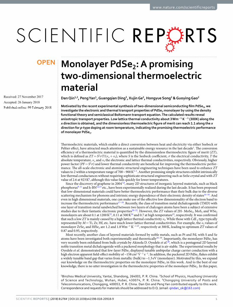
electrical conductivity σ, based on the CRTA Boltzmann theory. The left (right) panels of Fig. 4 show the trans-port coefficients along the x and y directions as a function of the electron (hole) concentration at T = 300 K. It is clear that the σ in Fig. 4(a,b) increases with the increasing carrier concentration while the magnitude of S in Fig. 4(c,d) decreases with doping. The electrical conductivity σ of monolayer PdSe2 exhibits remarkable aniso-tropic behaviors with (σy/σx) ~2.3 for n-type doping and (σx/σy) ~2.4 for p-type at 1.1 × 1013 cm−2 concentration. The calculated Seebeck coefficients along the x and y directions as a function of carrier concentration are shown in Fig. 4(c) and (d) for n- and p-type doping, respectively. We find a larger asymmetry of the Seebeck coefficient for p-type doping than for n-type doping, which is in good agreement with the recent report26. This anisot-ropy in the thermopower values in the two different directions might enable to design transverse thermoelctric device45. It is important to note that the Seebeck coefficients for both n- and p-type doped monolayer PdSe2 are substantially high at room temperature, reaching a peak value of 660 μV/K at an electron concentration around 1.25 × 1011 cm−2 and with an average value in the range of 300–340 μV/K. These values of S for monolayer PdSe2 compare favorably with those reported for some other 2D materials30,39. Figure 4(e) and (f) depict the power factor (PF) S2σ at room temperature along the x and y directions for n- and p-doped PdSe2 monolayer, respec-tively. The results reflect significant anisotropy in the power factor with the PFx/PFy ~1.9 for p-type doping and
Figure 4. Calculated thermoelectric transport coefficients σ (a,b), S (c,d), and S2σ (e,f) vs carrier concentration for n-(left panels) and p-type (right panels) doped PdSe2 along the x (black lines) and the y (red lines) directions at room temperature.
www.nature.com/scientificreports/
5Scientific REPORtS | (2018) 8:2764 | DOI:10.1038/s41598-018-20918-9
(PF)y/(PF)x ~2 for n-type doping at concentration around 1.1 × 1013 cm−2. The anisotropy in power factor arises from the large anistotropy of the conductivity and Seebeck coefficient for p and n types, as described above.
Phononic transport. Figure 2 shows the phonon dispersion relations of monolayer PdSe2 at its equilibrium volume along the high symmetric Γ − Y − M − X − Γ directions. It is noteworthy that the phonon spectrums of monolayer PdSe2 is very distinct from the MoS2 type monolayer. The maximum frequency of the acoustic mode markedly drop to rather low value of 3.7 THz, while for monolayers of MoSe2 and WSe2 it is 5.4 THz and 4.8 THz, respectively, and even higher for monolayer MoS2 with the value of 7.5 THz. Such low frequency suggests the low group velocity of acoustic modes in monolayer PdSe2. As acoustic modes contribute mostly to the lattice thermal conductivity κl, lower κl in this PdSe2 monolayer is expected.
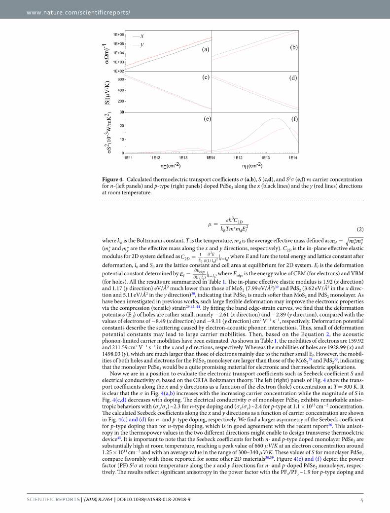
Now we turn to the computation of lattice thermal conductivity κl. As mentioned above, we estimate κl by means of the phonon Boltzmann transport equation and DFT as implemented in VASP and ShengBTE code. As presented by the fitted lines in Fig. 5, κl decreases following a T−1 dependence with the increasing temperature, suggesting that Umklapp phonon scattering dominates three-phonon interactions46. From the calculations, the obtained lattice thermal conductivity of monolayer PdSe2 is 3.7 (1.4) and 7.2 (2.7) Wm−1 K−1 at 300 K (800 K) along the x and y directions, respectively, which are much lower than MoS2
47 and GX2 monolayers48. It is obvious that the lattice thermal conductivity exhibits large directional anisotropy which may be due to differences in group velocity, anharmonicity and scattering phase space along the different directions.
Dimensionless figure of merit ZT. The electronic thermal conductivity κe of monolayer PdSe2 is calcu-lated via the Wiedemann-Franz law κe = L σT. Within the relaxation time approximation, the Seebeck coefficient can be calculated independently of the relaxation time τ, but evaluation of the electrical conductivity requires knowledge of τ. Here we take into account only the intrinsic scattering mechanism, namely, the interaction of electrons with acoustic phonons. Then the relaxation time τ can be evaluated from the equation τ = μm*/e, here the carrier mobility μ and effective mass m* have been calculated in subsection of Electronic transport properties, as listed in Table 1.
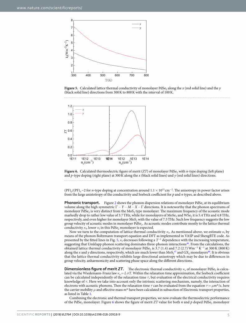
Combining the electronic and thermal transport properties, we now evaluate the thermoelectric performance of the PdSe2 monolayer. Figure 6 shows the figure of merit ZT value for both n and p doped PdSe2 monolayer
Figure 5. Calculated lattice thermal conductivity of monolayer PdSe2 along the x (red solid line) and the y (black solid line) directions from 300 K to 800 K with the interval of 100 K.
Figure 6. Calculated thermoelectric figure of merit (ZT) of monolayer PdSe2 with n-type doping (left plane) and p-type doping (right plane) at 300 K along the x (black solid lines) and y (red solid lines) directions.
www.nature.com/scientificreports/
6Scientific REPORtS | (2018) 8:2764 | DOI:10.1038/s41598-018-20918-9
along the x and y directions as a function of the carrier concentration at room temperature. We can see that the ZT values of n-type doped monolayer PdSe2 are rather small and almost isotropic with the maximum value of 0.13 with the corresponding concentration 3 × 1013 cm−2. However, for p-type doped monolayer PdSe2, ZT values exhibit the strong anisotropic property, with the value along the x direction being much larger than that along the y direction. The largest ZT value of 1.1 can be obtained in the x direction at the carrier concentration of 6.5 × 1012 cm−2 and 0.5 along the y direction at the carrier concentration of 2 × 1013 cm−2, respectively. Therefore, heavily doped p-type PdSe2 may offer excellent thermoelectric performance for applications such as powergener-ation. It is worthwhile to note that we have not considered the thermoelectric performance at higher temperature since the ZA mode of PdSe2 monolayer is very soft near point Γ, hence, it may be difficult to remain stable at high temperature. Usually, the thermoelectric performance at room temperature is the most importantly information we need for it is better to discover thermoelectric materials working under room temperature.
ConclusionIn summary, by means of first-principles calculation, the geometrical structure, mechanical, electronic and ther-mal transport properties of monolayer PdSe2 are systematically investigated. In contrast to TMCs, monolayer PdSe2 has strong anisotropic mechanical, electronic and thermal transport properties, leading to anisotropic thermoelectric properties. We find that PdSe2 is a semiconductor with an indirect band gap of 1.38 eV and a hole mobility as high as 1929 cm 2 V−1 s−1. The in-plane effective elastic modulus are rather low, suggesting the flexible mechanical properties in this structure. Furthermore, monolayer PdSe2 has a low lattice thermal conductivity about 3 Wm−1 K−1 along the x direction at room temperature. Combining its high Seebeck coefficient and mark-edly low thermal conductivity, monolayer PdSe2 shows an optimum ZT value of 1.1 (300K) at optimal doping. Therefore, our results indicate monolayer PdSe2 is a material with promising thermoelectric performance.
Computational MethodsThe initial structure of monolayer PdSe2 is optimized through DFT with the plane-wave based Vienna ab-initio simulation package (VASP)49,50, using the projector augmented wave (PAW) method. For the exchange-correlation functional, we have used the Perdew-Burke-Ernzerhof version of the generalized gradient approximation (GGA)51. A plane-wave cutoff energy of 400 eV and an energy convergence criterion of 10−7 eV are adopted throughout calculations. The spin-orbit coupling (SOC) is not considered in the structure relaxation. For ionic relaxation calculations, a 11 × 11 × 1 Monkhorst-Pack k-meshes52 are used and the structure is considered to be stable when the Hellmann-Feynman forces are smaller than 0.001 eV/Å. For the slab model, a 21 Å thick vacuum layer was used to avoid the interactions between adjacent monolayers.
After determining the equilibrium structure, we have performed electronic structure calculations employ-ing the all-electron full-potential WIEN2k code53 using recently implemented Tran and Blaha’s modified Becke-Johnson (TB-mBJ)54 exchange potential plus generalised gradient approximation (GGA) with the SOC included. The TB-mBJGGA potential for electronic properties and band gap with higher accuracy and less com-putational effort as compared to hybrid functional and GW overcomes the shortcoming of underestimation of energy gap in both LDA and GGA approximations55. The number of plane waves in a Fourier expansion of poten-tial in the interstitial region was restricted to RMT × Kmax = 8. The muffin tin radii for Se and Pd are 2.1 and 2.2 a.u., respectively. We used 19 × 19 × 1 k-point Monkhorst-Pack mesh for electronic band structure calculations.
Based on the self-consistent converged electronic structure calculations, we have employed the eigenener-gies on a very dense nonshifted 8000 k-point mesh in the full Brillouin zone (BZ). Thermoelectrical transport properties were calculated by solving the Boltzmann transport equations within the rigid band (RBA) and con-stant relaxation-time approximations (CRTA) as implemented in the BoltzTraP software56, which neglects the weak energy dependence of relaxation time but retains some temperature and doping dependence57. This CRTA approach has been tested earlier and found to work quite well in calculating the Seebeck coefficient in a variety of thermoelectric materials even for materials with highly anisotropic crystal axes58–61. A comprehensive descrip-tion of the Boltzmann transport theory in the relaxation time approximation can be found elsewhere23. A brief summary of formalism used in this work is provided below62. The energy projected transport distribution (TD) tensor is defined as
∑σ ε τ δ ε ε= −αβ α βeN
v i k v i k( ) ( , ) ( , ) ( )(3)i k
i k i k
2
,, ,
where group velocity
=αε∂
∂ αv i k( , )
k1 i k, , N is the number of k-points sampled, τi, k is the band index i and wave
vector k dependent relaxation time, α and β are the Cartesian indices, and e is the electron charge. Then the elec-trical conductivity and Seebeck coefficient as a function of temperation T and chemical potential μ, can be written as
∫σ μ σ εε μ
εε=
Ω
−
∂
∂
αβ αβT
f Td( , ) 1 ( )
( , , )
(4)0
∫μ σ μ σ ε ε με μ
εε=
Ω− ×
−
∂
∂
αβ αβ αβS T
e TT
f Td( , ) 1 ( , ) ( )( )
( , , )
(5)20
where Ω is the volume of unit cell and f0 is the Fermi-Dirac distribution function. Thus, by using the CRTA, τ is exactly cancelled out in Equation 5. From the above calculations we can obtain the Seebeck coefficient
www.nature.com/scientificreports/
7Scientific REPORtS | (2018) 8:2764 | DOI:10.1038/s41598-018-20918-9
S and the electrical conductivity over relaxation time (σ/τ) as well. The electronic thermal conductivity ke is calculated using the Wiedemann-Franz law, ke = L σT, where L is the Lorenz number. In our calculations we use L = 2.4 × 10⁻⁸ J2 K−2 C−2 63.
To confirm the dynamic stability of the PdSe2 monolayer, we have calculated the phonon spectrum using a finite displacement method implemented the Phonopy code interfaced with the VASP code50,64. At the same time the second-order harmonic IFCs of monolayer PdSe2 and third order anharmonic IFCs were calculated using a 4 × 4 × 1 supercell and a 3 × 3 × 1 supercell with Γ point, respectively. Based on an adaptive smearing approach to the conservation of energy65 and with an iterative solution method66, we then solved the phonon Boltzmann transport equation using ShengBTE67.
References 1. Bell, L. E. Cooling, heating, generating power, and recovering waste heat with thermoelectric systems. Science 321, 1457–1461
(2008). 2. Hsu, K. F. et al. Cubic agpbmsbte2+m: Bulk thermoelectric materials with high figure of merit. Science 303, 818–821 (2004). 3. Biswas, K. et al. High-performance bulk thermoelectrics with all-scale hierarchical architectures. Nature 489, 414–418 (2012). 4. Rhyee, J.-S. et al. Peierls distortion as a route to high thermoelectric performance in In4se3-[dgr] crystals. Nature 459, 965–968
(2009). 5. Zhao, L., Dravid, V. & Kanatzidis, M. The panoscopic approach to high performance thermoelectrics. Energ environ sci 7, 251–268
(2014). 6. Zhao, L.-D. et al. Ultralow thermal conductivity and high thermoelectric figure of merit in snse crystals. Nature 508, 373–377
(2014). 7. Novoselov, K. S. et al. Electric field effect in atomically thin carbon films. Science 306, 666–669 (2004). 8. Kane, C. L. Materials science: Erasing electron mass. Nature 438, 168–170 (2005). 9. Li, L. et al. Black phosphorus field-effect transistors. NatNano 9, 372–377 (2014). 10. Liu, H. et al. Phosphorene: An unexplored 2d semiconductor with a high hole mobility. ACS Nano 8, 4033–4041 (2014). 11. Xia, F., Wang, H. & Jia, Y. Rediscovering black phosphorus as an anisotropic layered material for optoelectronics and electronics.
Nat. Commun. 5, 4458 (2014). 12. Zhi, C., Bando, Y., Tang, C., Kuwahara, H. & Golberg, D. Large-scale fabrication of boron nitride nanosheets and their utilization in
polymeric composites with improved thermal and mechanical properties. Adv. Mater. 21, 2889–2893 (2009). 13. Warner, J. H., Rümmeli, M. H., Bachmatiuk, A. & Büchner, B. Atomic resolution imaging and topography of boron nitride sheets
produced by chemical exfoliation. ACS Nano 4, 1299–1304 (2010). 14. He, J., Kanatzidis, M. G. & Dravid, V. P. High performance bulk thermoelectrics via a panoscopic approach. Mater.Today 16,
166–176 (2013). 15. Zhang, J. et al. Phosphorene nanoribbon as a promising candidate for thermoelectric applications. Sci. Rep. 4, 6452 (2014). 16. Park, K. H., Martin, P. N. & Ravaioli, U. Electronic and thermal transport study of sinusoidally corrugated nanowires aiming to
improve thermoelectric efficiency. Nat 27, 035401 (2016). 17. Wu, L. et al. Two-dimensional thermoelectrics with Rashba spin-split bands in bulk BiTeI. Phys. Rev. B 90, 195210 (2014). 18. Mi, X.-Y. et al. Enhancing the Thermoelectric Figure of Merit by Low-Dimensional Electrical Transport in Phonon-Glass Crystals.
Nano Lett. 15, 5229–5234 (2015). 19. Bilc, D. I., Hautier, G., Waroquiers, D., Rignanese, G.-M. & Ghosez, P. Low-dimensional transport and large thermoelectric power
factors in bulk semiconductors by band engineering of highly directional electronic states. Phys. Rev. Lett. 114, 136601 (2015). 20. Butler, S. Z. et al. Progress, challenges, and opportunities in two-dimensional materials beyond graphene. ACS Nano 7, 2898–2926
(2013). 21. Xu, M., Liang, T., Shi, M. & Chen, H. Graphene-like two-dimensional materials. Chem. Rev. 113, 3766–3798 (2013). 22. Kuc, A. & Heine, T. The electronic structure calculations of two-dimensional transition-metal dichalcogenides in the presence of
external electric and magnetic fields. Chem. Soc. Rev. 44, 2603–2614 (2015). 23. Kumar, S. & Schwingenschlӧgl, U. Thermoelectric response of bulk and monolayer MoSe2 and Wse2. Chem. Mater. 27, 1278–1284
(2015). 24. Jin, Z. et al. A revisit to high thermoelectric performance of single-layer MoS2. Sci. Rep. 5 (2016). 25. Ding, G., Gao, G. Y., Huang, Z., Zhang, W. & Yao, K. Thermoelectric properties of monolayermse2(m = zr, hf): low lattice thermal
conductivity and a promising figure of merit. Nat 27, 375703 (2016). 26. Sun, J., Shi, H., Siegrist, T. & Singh, D. J. Electronic, transport, and optical properties of bulk and mono-layer PdSe2. Appl. Phys. Lett.
107, 153902 (2015). 27. Chow, W. L. et al. High mobility 2d palladium diselenide field-effect transistors with tunable ambipolar characteristics. Adv. Mater.
29, 14090–14097 (2017). 28. Oyedele, A. et al. Pdse2: Pentagonal 2d layers with high air stability for electronics. J.Am.Chem.Soc. 0, null (0). 29. Ahmad, S. Strain dependent tuning electronic properties of noble metal di chalcogenidespdx2(x = s,se)monolayer. Mater. Chem.
Phys. 198, 162–166 (2017). 30. Wang, Y., Li, Y. & Chen, Z. Not your familiar two dimensional transition metal disulfide: structural and electronic properties of the
PdS2 monolayer. J. Mater. Chem. C 3, 9603–9608 (2015). 31. Soulard, C. et al. Experimental and Theoretical Investigation on the Relative Stability of the PdS2- and Pyrite-Type Structures of
PdSe2. Inorganic Chemistry 43, 1943–1949 (2004). 32. Grønvold, F. & Røst, E. The crystal structure of PdSe2 and PdS2. Acta Crystallographica 10, 329–331 (1957). 33. Baroni, S., de Gironcoli, S., Dal Corso, A. & Giannozzi, P. Phonons and related crystal properties from density-functional
perturbation theory. Rev. Mod. Phys. 73, 515–562 (2001). 34. Lebègue, S., Björkman, T., Klintenberg, M., Nieminen, R. M. & Eriksson, O. Two-dimensional materials from data filtering and ab
initio calculations. Phys. Rev. X 3, 031002 (2013). 35. Pei, Y., LaLonde, A. D., Wang, H. & Snyder, G. J. Low effective mass leading to high thermoelectric performance. Energy &
Environmental Science 5, 7963 (2012). 36. Beleznay, F., Bogár, F. & Ladik, J. Charge carrier mobility in quasi-one-dimensional systems: Application to a guanine stack. J. Chem.
Phys. 119, 5690–5695 (2003). 37. Zhang, L.-C. et al. Tinselenidene: a two-dimensional auxetic material with ultralow lattice thermal conductivity and ultrahigh hole
mobility. Sci. Rep. 6 (2016). 38. Long, M., Tang, L., Wang, D., Li, Y. & Shuai, Z. Electronic structure and carrier mobility in graphdiyne sheet and nanoribbons:
Theoretical predictions. ACS Nano 5, 2593–2600 (2011). 39. Cai, Y., Zhang, G. & Zhang, Y.-W. Polarity-reversed robust carrier mobility in monolayer mos2 nanoribbons. J.Am.Chem.Soc. 136,
6269–6275 (2014). 40. Qiao, J., Kong, X., Hu, Z.-X., Yang, F. & Ji, W. High-mobility transport anisotropy and linear dichroism in few-layer black
phosphorus. Nat. Commun. 5 (2014).
www.nature.com/scientificreports/
8Scientific REPORtS | (2018) 8:2764 | DOI:10.1038/s41598-018-20918-9
41. Wang, Y. et al. Monolayerptse2, a new semiconducting transition-metal-dichalcogenide, epitaxially grown by direct selenization of pt. Nano Letters 15, 4013–4018 (2015).
42. Qin, D., Ge, X.-J., Ding, G.-Q., Gao, G.-Y. & Lü, J.-T. Strain-induced thermoelectric performance enhancement of monolayer ZrSe2. RSC Adv. 7, 47243–47250 (2017).
43. Guo, H., Lu, N., Wang, L., Wu, X. & Zeng, X. C. Tuning electronic and magnetic properties of early transition-metal dichalcogenides via tensile strain. J.Phys.Chem. C 118, 7242–7249 (2014).
44. Guo, S.-D. Biaxial strain tuned thermoelectric properties in monolayer PtSe2. J. Mater. Chem. C. 4, 9366–9374 (2016). 45. Zhou, C., Birner, S., Tang, Y., Heinselman, K. & Grayson, M. Driving perpendicular heat flow: (p×n)-type transverse thermoelectrics
for microscale and cryogenic peltier cooling. Phys. Rev. Lett. 110, 227701 (2013). 46. Ward, A., Broido, D. A., Stewart, D. A. & Deinzer, G. Ab initio. Phys. Rev. B 80, 125203 (2009). 47. Yan, R. et al. Thermal Conductivity of Monolayer Molybdenum Disulfide Obtained from Temperature-Dependent Raman
Spectroscopy. ACS Nano 8, 986–993 (2014). 48. Ge, X.-J., Qin, D., Yao, K.-L. & Lü, J.-T. First-principles study of thermoelectric transport properties of monolayer gallium
chalcogenides. Journal of Physics D: Applied Physics 50, 405301 (2017). 49. Kresse, G. & Hafner, J. Ab initio. Phys. Rev. B 47, 558–561 (1993). 50. Kresse, G. & Furthmüller, J. Efficient iterative schemes for ab initio total-energy calculations using a plane-wave basis set. Phys. Rev.
B 54, 11169 (1996). 51. Perdew, J. P., Burke, K. & Ernzerhof, M. Generalized gradient approximation made simple. Phys. Rev. Lett. 77, 3865–3868 (1996). 52. Monkhorst, H. J. & Pack, J. D. Special points for brillouin-zone integrations. Phys. Rev. B 13, 5188–5192 (1976). 53. Blaha, P., Schwarz, K., Madsen, G., Kvasnicka, D. &Luitz, J. wien2k. WIEN2k An augmented plane wave + local orbitals program for
calculating crystal properties (2001). 54. Tran, F. & Blaha, P. Accurate band gaps of semiconductors and insulators with a semilocal exchange-correlation potential. Phys. Rev.
Lett. 102, 226401 (2009). 55. Kim, Y.-S., Marsman, M., Kresse, G., Tran, F. & Blaha, P. Towards efficient band structure and effective mass calculations for iii-v
direct band-gap semiconductors. Phys. Rev. B 82, 205212 (2010). 56. Madsen, G. K. & Singh, D. J. Boltztrap. a code for calculating band-structure dependent quantities. Comput. Phys. Commun. 175,
67–71 (2006). 57. Parker, D. & Singh, D. J. Potential thermoelectric performance from optimization of hole-doped bi2se3. Phys. Rev. X 1, 021005
(2011). 58. Xi, L. et al. Chemical bonding, conductive network, and thermoelectric performance of the ternary semiconductors cu2snX3 (x = se,
s) from first principles. Phys. Rev. B 86, 155201 (2012). 59. Singh, D. J. Electronic and thermoelectric properties of CuCoo2: Density functional calculations. Phys. Rev. B 76, 085110 (2007). 60. Parker, D. & Singh, D. J. High-temperature thermoelectric performance of heavily doped pbse. Phys. Rev. B 82, 035204 (2010). 61. Wang, Y. et al. Enhanced thermoelectric performance of pbte within the orthorhombic pnma phase. Phys. Rev. B 76, 155127 (2007). 62. Scheidemantel, T. J., Ambrosch-Draxl, C., Thonhauser, T., Badding, J. V. & Sofo, J. O. Transport coefficients from first-principles
calculations. Phys. Rev. B 68, 125210 (2003). 63. Parlinski, K., Li, Z. Q. & Kawazoe, Y. First-principles determination of the soft mode in cubic zero2. Phys. Rev. Lett. 78, 4063–4066
(1997). 64. Togo, A., Oba, F. & Tanaka, I. First-principles calculations of the ferroelastic transition between rutile-type and cacl 2-type sio 2 at
high pressures. Phys. Rev. B 78, 134106 (2008). 65. Li, W. et al. Thermal conductivity of diamond nanowires from first principles. Phys. Rev. B 85, 195436 (2012). 66. Li, W., Lindsay, L., Broido, D., Stewart, D. A. & Mingo, N. Thermal conductivity of bulk and nanowire mg 2 si x sn 1- x alloys from
first principles. Phys. Rev. B 86, 174307 (2012). 67. Li, W., Carrete, J., Katcho, N. A. & Mingo, N. Shengbte: A solver of the boltzmann transport equation for phonons. Comput. Phys.
Commun. 185, 1747–1758 (2014).
AcknowledgementsThe authors gratefully acknowledge the financial supports from the National Natural Science Foundation of China (Grant No. 51401031).
Author ContributionsD.Q. and P.Y. conceived and designed the research. D.Q. carried out the calculations and analyzed the calculated results with the helps from P.Y., G.Q.D., X.J.G. and H.Y.S. discussed the related calculated results. All authors reviewed the manuscript.
Additional InformationCompeting Interests: The authors declare no competing interests.Publisher's note: Springer Nature remains neutral with regard to jurisdictional claims in published maps and institutional affiliations.
Open Access This article is licensed under a Creative Commons Attribution 4.0 International License, which permits use, sharing, adaptation, distribution and reproduction in any medium or
format, as long as you give appropriate credit to the original author(s) and the source, provide a link to the Cre-ative Commons license, and indicate if changes were made. The images or other third party material in this article are included in the article’s Creative Commons license, unless indicated otherwise in a credit line to the material. If material is not included in the article’s Creative Commons license and your intended use is not per-mitted by statutory regulation or exceeds the permitted use, you will need to obtain permission directly from the copyright holder. To view a copy of this license, visit http://creativecommons.org/licenses/by/4.0/. © The Author(s) 2018


