Embed Size (px)
Citation preview
MAHARASHTRA STATE BOARD OF TECHNICAL EDUCATION (Autonomous)
(ISO/IEC - 27001 - 2013 Certified)
__________________________________________________________________________________________________
Page 1 of 31
WINTER– 17 EXAMINATION Subject Name: Microcontroller Model Answer Subject Code:
I m p o r t a n t I n s t r u c t i o n s t o e x a m i n e r s : 1) The answers should be examined by key words and not as word-to-word as given in the
model answer scheme. 2) The model answer and the answer written by candidate may vary but the examiner may
try to assess the understanding level of the candidate. 3) The language errors such as grammatical, spelling errors should not be given more
Importance (Not applicable for subject English and Communication Skills. 4) While assessing figures, examiner may give credit for principal components indicated in
the figure. The figures drawn by candidate and model answer may vary. The examiner may give credit for any equivalent figure drawn.
5) Credits may be given step wise for numerical problems. In some cases, the assumed constant values may vary and there may be some difference in the candidate’s answers and model answer.
6) In case of some questions credit may be given by judgement on part of examiner of relevant answer based on candidate’s understanding.
7) For programming language papers, credit may be given to any other program based on equivalent concept.
17534
MAHARASHTRA STATE BOARD OF TECHNICAL EDUCATION (Autonomous)
(ISO/IEC - 27001 - 2013 Certified)
__________________________________________________________________________________________________
Page 2 of 31
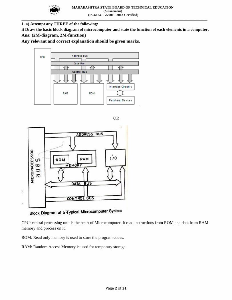
1. a) Attempt any THREE of the following:
i) Draw the basic block diagram of microcomputer and state the function of each elements in a computer.
Ans: (2M-diagram, 2M-function)
Any relevant and correct explanation should be given marks.
OR
CPU: central processing unit is the heart of Microcomputer. It read instructions from ROM and data from RAM
memory and process on it.
ROM: Read only memory is used to store the program codes.
RAM: Random Access Memory is used for temporary storage.
MAHARASHTRA STATE BOARD OF TECHNICAL EDUCATION (Autonomous)
(ISO/IEC - 27001 - 2013 Certified)
__________________________________________________________________________________________________
Page 3 of 31
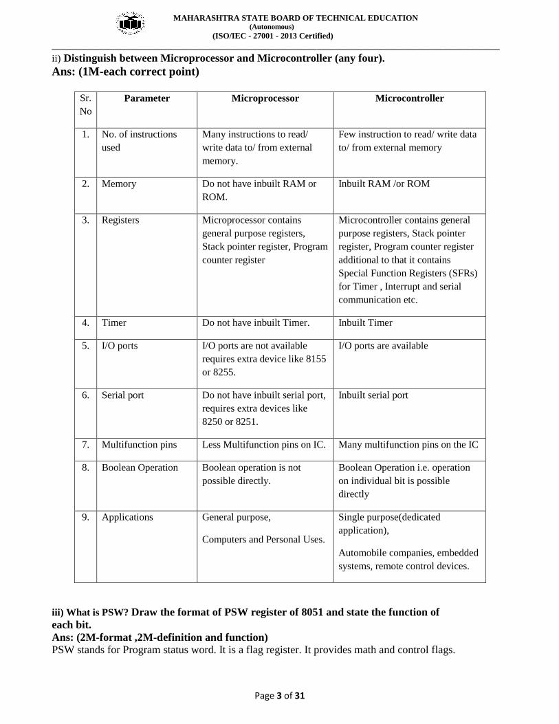
ii) Distinguish between Microprocessor and Microcontroller (any four).
Ans: (1M-each correct point)
Sr.
No
Parameter Microprocessor Microcontroller
1. No. of instructions
used
Many instructions to read/
write data to/ from external
memory.
Few instruction to read/ write data
to/ from external memory
2. Memory Do not have inbuilt RAM or
ROM.
Inbuilt RAM /or ROM
3. Registers Microprocessor contains
general purpose registers,
Stack pointer register, Program
counter register
Microcontroller contains general
purpose registers, Stack pointer
register, Program counter register
additional to that it contains
Special Function Registers (SFRs)
for Timer , Interrupt and serial
communication etc.
4. Timer Do not have inbuilt Timer. Inbuilt Timer
5. I/O ports I/O ports are not available
requires extra device like 8155
or 8255.
I/O ports are available
6. Serial port Do not have inbuilt serial port,
requires extra devices like
8250 or 8251.
Inbuilt serial port
7. Multifunction pins Less Multifunction pins on IC. Many multifunction pins on the IC
8. Boolean Operation Boolean operation is not
possible directly.
Boolean Operation i.e. operation
on individual bit is possible
directly
9. Applications General purpose,
Computers and Personal Uses.
Single purpose(dedicated
application),
Automobile companies, embedded
systems, remote control devices.
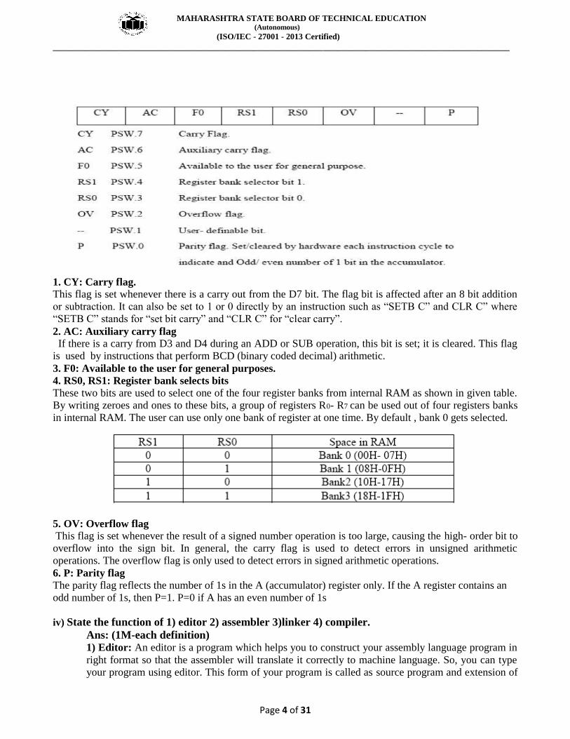
iii) What is PSW? Draw the format of PSW register of 8051 and state the function of
each bit.
Ans: (2M-format ,2M-definition and function)
PSW stands for Program status word. It is a flag register. It provides math and control flags.
MAHARASHTRA STATE BOARD OF TECHNICAL EDUCATION (Autonomous)
(ISO/IEC - 27001 - 2013 Certified)
__________________________________________________________________________________________________
Page 4 of 31
1. CY: Carry flag. This flag is set whenever there is a carry out from the D7 bit. The flag bit is affected after an 8 bit addition
or subtraction. It can also be set to 1 or 0 directly by an instruction such as “SETB C” and CLR C” where
“SETB C” stands for “set bit carry” and “CLR C” for “clear carry”.
2. AC: Auxiliary carry flag If there is a carry from D3 and D4 during an ADD or SUB operation, this bit is set; it is cleared. This flag
is used by instructions that perform BCD (binary coded decimal) arithmetic.
3. F0: Available to the user for general purposes.
4. RS0, RS1: Register bank selects bits These two bits are used to select one of the four register banks from internal RAM as shown in given table.
By writing zeroes and ones to these bits, a group of registers R0- R7 can be used out of four registers banks
in internal RAM. The user can use only one bank of register at one time. By default , bank 0 gets selected.
5. OV: Overflow flag This flag is set whenever the result of a signed number operation is too large, causing the high- order bit to
overflow into the sign bit. In general, the carry flag is used to detect errors in unsigned arithmetic
operations. The overflow flag is only used to detect errors in signed arithmetic operations.
6. P: Parity flag The parity flag reflects the number of 1s in the A (accumulator) register only. If the A register contains an
odd number of 1s, then P=1. P=0 if A has an even number of 1s
iv) State the function of 1) editor 2) assembler 3)linker 4) compiler.
Ans: (1M-each definition) 1) Editor: An editor is a program which helps you to construct your assembly language program in
right format so that the assembler will translate it correctly to machine language. So, you can type
your program using editor. This form of your program is called as source program and extension of
MAHARASHTRA STATE BOARD OF TECHNICAL EDUCATION (Autonomous)
(ISO/IEC - 27001 - 2013 Certified)
__________________________________________________________________________________________________
Page 5 of 31
program must be .asm or .src depending on which assembler is used. The DOS based editor such as
EDIT, WordStar, and Norton Editor etc. can be used to type your program.
2) Assembler: An assembler is programs that translate assembly language program to the correct
binary/hex code for each instruction i.e. machine code and generate the file called as Object file
with extension .obj and list file with extension .lst extension.
It is used to find syntax error in the program.
Some examples of assembler are ASEM-51, Kiel’s A51, AX 51 and C51, Intel PL/M-51 etc.
3) Compiler: Compiler is programs that translate C language program to the correct binary/hex
code for each command i.e. machine code and generate the file called as Object file with
extension .obj and list file with extension .lst extension.
It is used to find syntax error in the program. 4) Linker: A linker is a program, which combines, if requested, more than one separately
assembled object files into one executable program, such as two or more programs and also
generate .abs file and initializes it with special instructions to facilitate its subsequent loading the
execution.
Some examples of linker are ASEM-51 BL51, Keil u Vision Debugger, LX 51 Enhanced Linker
etc.
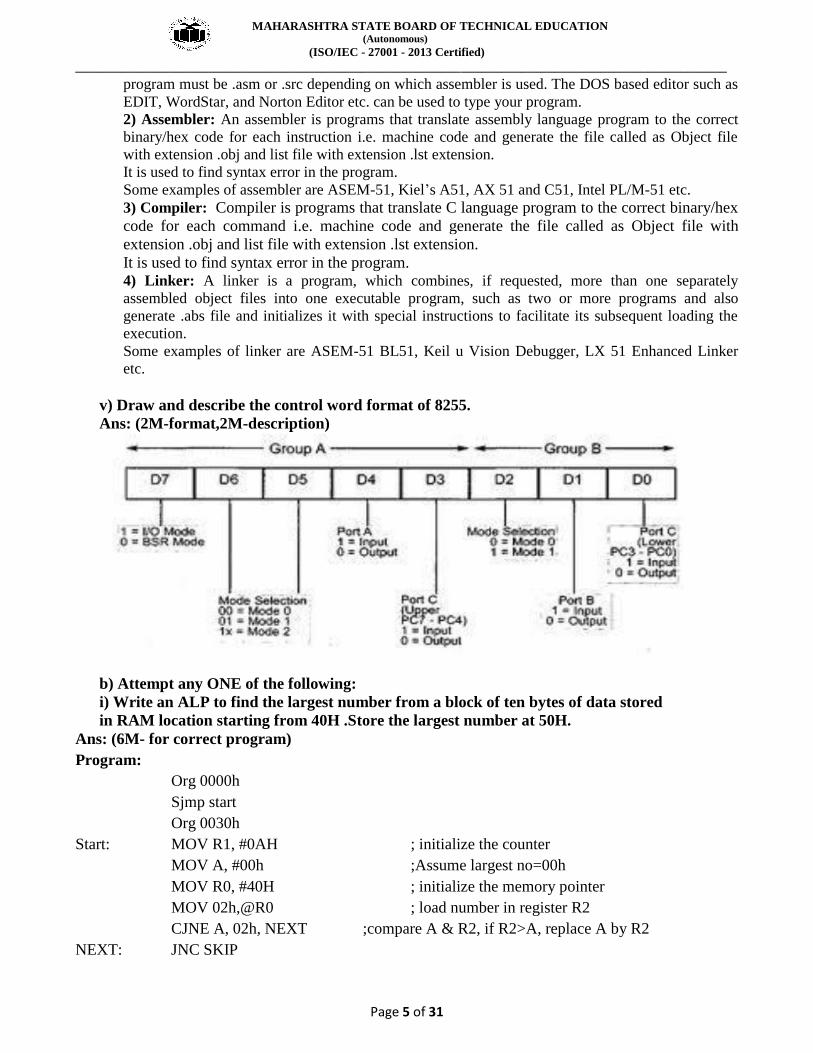
v) Draw and describe the control word format of 8255.
Ans: (2M-format,2M-description)
b) Attempt any ONE of the following:
i) Write an ALP to find the largest number from a block of ten bytes of data stored
in RAM location starting from 40H .Store the largest number at 50H.
Ans: (6M- for correct program)
Program:
Org 0000h
Sjmp start
Org 0030h
Start: MOV R1, #0AH ; initialize the counter
MOV A, #00h ;Assume largest no=00h
MOV R0, #40H ; initialize the memory pointer
MOV 02h,@R0 ; load number in register R2
CJNE A, 02h, NEXT ;compare A & R2, if R2>A, replace A by R2
NEXT: JNC SKIP
MAHARASHTRA STATE BOARD OF TECHNICAL EDUCATION (Autonomous)
(ISO/IEC - 27001 - 2013 Certified)
__________________________________________________________________________________________________
Page 6 of 31
MOV A, R2
SKIP: INC R0 ; increment the memory pointer
DJNZ R1, UP ; decrement the counter by one, if count
≠0, then go to UP
MOV 50H, A ; store result at memory location 50H
HERE: SJMP HERE
END
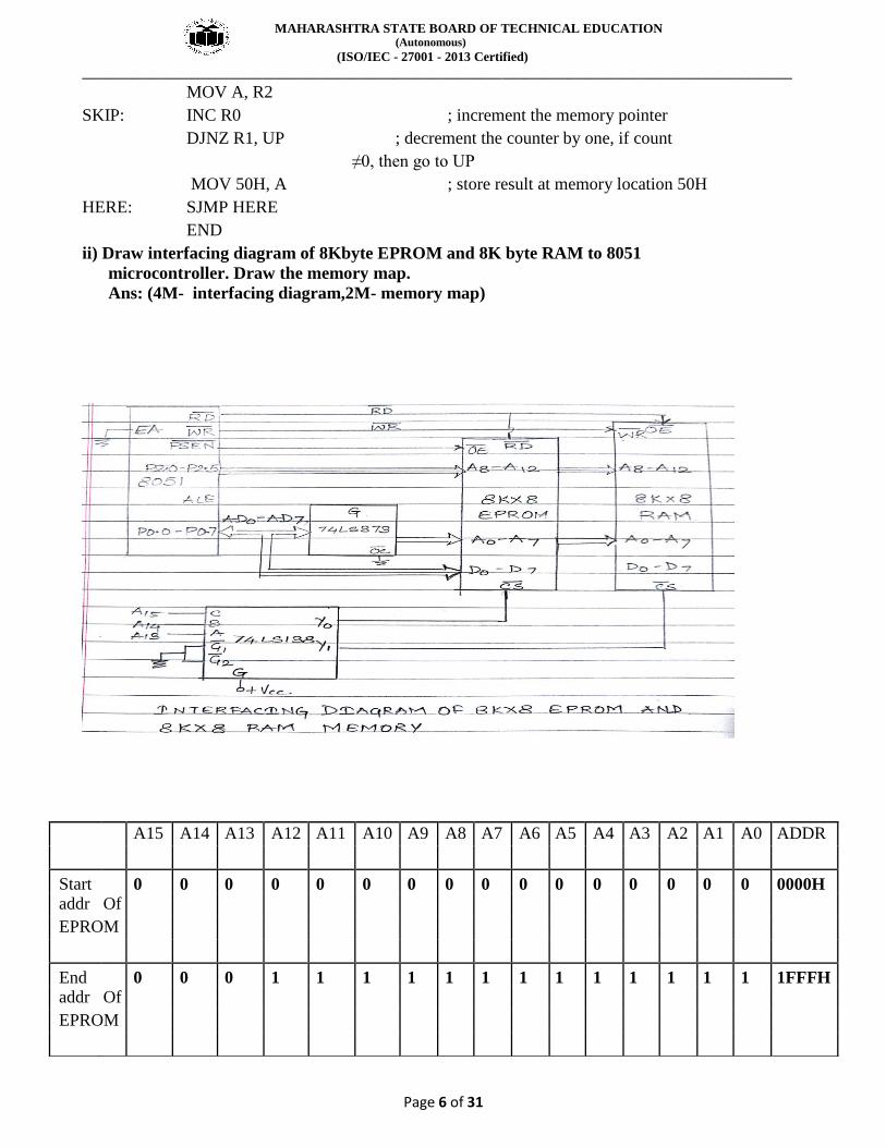
ii) Draw interfacing diagram of 8Kbyte EPROM and 8K byte RAM to 8051
microcontroller. Draw the memory map.
Ans: (4M- interfacing diagram,2M- memory map)
A15 A14 A13 A12 A11 A10 A9 A8 A7 A6 A5 A4 A3 A2 A1 A0 ADDR
Start 0 0 0 0 0 0 0 0 0 0 0 0 0 0 0 0 0000H addr Of
EPROM
End 0 0 0 1 1 1 1 1 1 1 1 1 1 1 1 1 1FFFH addr Of
EPROM
MAHARASHTRA STATE BOARD OF TECHNICAL EDUCATION (Autonomous)
(ISO/IEC - 27001 - 2013 Certified)
__________________________________________________________________________________________________
Page 7 of 31
Note:1) If CS of both RAM and ROM is connected to ground is also correct. As 8051 is Harvard
architecture, there is separate space for RAM and ROM therefore starting address of RAM is
0000h as well as for ROM also 0000h. students can use different decoding logic for /CS.
2) /RD of EPROM is to be connected to /PSEN and not to /RD.
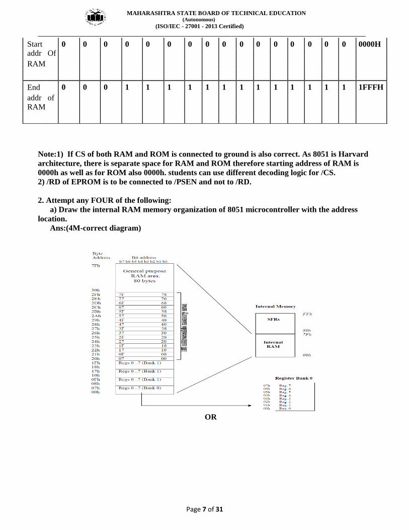
2. Attempt any FOUR of the following:
a) Draw the internal RAM memory organization of 8051 microcontroller with the address
location.
Ans:(4M-correct diagram)
OR
Start 0 0 0 0 0 0 0 0 0 0 0 0 0 0 0 0 0000H addr Of
RAM
End 0 0 0 1 1 1 1 1 1 1 1 1 1 1 1 1 1FFFH
addr of
RAM
MAHARASHTRA STATE BOARD OF TECHNICAL EDUCATION (Autonomous)
(ISO/IEC - 27001 - 2013 Certified)
__________________________________________________________________________________________________
Page 8 of 31
b) Compare 8031,8051and 8751( four points)
Ans: 1M each- for correct point)
specification 8031 8051 8751
On chip data memory 128 byte 128 byte 128 byte
MAHARASHTRA STATE BOARD OF TECHNICAL EDUCATION (Autonomous)
(ISO/IEC - 27001 - 2013 Certified)
__________________________________________________________________________________________________
Page 9 of 31
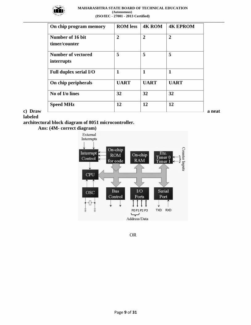
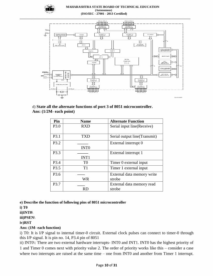
c) Draw a neat
labeled
architectural block diagram of 8051 microcontroller.
Ans: (4M- correct diagram)
OR
On chip program memory ROM less 4K ROM 4K EPROM
Number of 16 bit
timer/counter
2 2 2
Number of vectored
interrupts
5 5 5
Full duplex serial I/O 1 1 1
On chip peripherals UART UART UART
No of I/o lines 32 32 32
Speed MHz 12 12 12
MAHARASHTRA STATE BOARD OF TECHNICAL EDUCATION (Autonomous)
(ISO/IEC - 27001 - 2013 Certified)
__________________________________________________________________________________________________
Page 10 of 31
d) State all the alternate functions of port 3 of 8051 microcontroller.
Ans: (1/2M- each point)
Pin Name Alternate Function
P3.0 RXD Serial input line(Receive)
P3.1 TXD Serial output line(Transmit)
P3.2
INT0
External interrupt 0
P3.3
INT1
External interrupt 1
P3.4 T0 Timer 0 external input
P3.5 T1 Timer 1 external input
P3.6
WR
External data memory write
strobe
P3.7
RD
External data memory read
strobe
e) Describe the function of following pins of 8051 microcontroller
i) T0
ii)INT0\
iii)PSEN\
iv)RST
Ans: (1M- each function)
i) T0: It is I/P signal to internal timer-0 circuit. External clock pulses can connect to timer-0 through
this I/P signal. It is pin no. 14, P3.4 pin of 8051
ii) INT0\: There are two external hardware interrupts- INT0 and INT1. INT0 has the highest priority of
1 and Timer 0 comes next with priority value 2. The order of priority works like this – consider a case
where two interrupts are raised at the same time – one from INT0 and another from Timer 1 interrupt.
MAHARASHTRA STATE BOARD OF TECHNICAL EDUCATION (Autonomous)
(ISO/IEC - 27001 - 2013 Certified)
__________________________________________________________________________________________________
Page 11 of 31
In such a case, processor would serve the interrupt according to it’s priority. In our case INT0 is of high
priority (priority order 1)and Timer 1 interrupt is of low priority (priority order 4). So processor will
execute ISR of INTO first and then later, after finishing ISR of INT0, processor will begin executing
ISR of Timer 1 interrupt.
iii) PSEN\: PSEN stands for “program store enable.” In an 8031-based system in which an external
ROM holds the program code, this pin is connected to the /OE pin of the ROM. In other words, to
access external ROM containing program code, the 8031/51 uses the PSEN signal. When the EA pin is
connected to GND, the 8031/51 fetches opcode from external ROM by using PSEN. In systems based
on the 8751/89C51/ DS5000 where EA is connected to VCC, these chips do not activate the PSEN pin.
This indicates that the on- chip ROM contains program code.
iv) RST: RST stands for reset. The RST pin of 8051 is made high for two machine cycles, while the
oscillator is running. A power on reset circuit is used. A pull down resistor of 8.2K form the RST pin to
Vss and a capacitor of 10uf from the reset circuit. These component values are sufficient to provide a
delay, so as to make the RST line high for 24 oscillations. To support the manual reset function, if
desired so, a switch may be added across the 10uf capacitor.
f) Compare Von-Neumann and Harvard architecture (Four points)
Ans: 1M-each correct point
Q3 Attempt any four of the following
MAHARASHTRA STATE BOARD OF TECHNICAL EDUCATION (Autonomous)
(ISO/IEC - 27001 - 2013 Certified)
__________________________________________________________________________________________________
Page 12 of 31
a) What are assembler directives? State and describe any three directives with one example
each
Ans ( 1 mark assembler directives , 1 M each directive any three 3 marks )
. Unlike instructions being compiled and written to chip program memory, directives are commands
of assembly language itself and have no influence on the operation of the microcontroller. Some of
them are obligatory part of every program while some are used only to facilitate or speed up the
operation. Directives are written in the column reserved for instructions. There is a rule allowing
only one directive per program line.
1) ORG: ORG stands for Origin
Syntax:
ORG Address
The ORG directive is used to indicate the beginning of the address. The number that comes after ORG can be either in hex or in decimal. If the number is not followed by H, it is decimal and the assembler will convert it to hex. Some assemblers use ―.ORG‖ (notice the dot) instead of ―ORG‖ for the origin directive.
2) DB:- (Data Byte)
Syntax:
Label: DB Byte
Where byte is an 8-bit number represented in either binary, Hex, decimal or ASCII form. There should be at least one space between label & DB. The colon (:) must present after label. This directive can be used at the beginning of program. The label will be used in program instead of actual byte. There should be at least one space between DB & a byte. Following are some DB examples:
LOOKUP: DB 30h,31h,32h,33h,34h,35h
3) EQU: Equate
Format
LABEL EQU ADDRESS
e.g.
VALUE EQU 60h
MOV VALUE,#25h
4) END:
This assembler directive is used to end the program. No commands or instructions will
be accepted after end.
5) CODE directive
The CODE directive is used to assign a symbol to a program memory address. Since the
maximum capacity of program memory is 64K, the address must be in the range of 0 to 65535.
MAHARASHTRA STATE BOARD OF TECHNICAL EDUCATION (Autonomous)
(ISO/IEC - 27001 - 2013 Certified)
__________________________________________________________________________________________________
Page 13 of 31
6) DATA:
Syntax:
By means of this directive an address with internal RAM is designated as a symbol (address must
be in the range of 0-255). In other words, any selected register may change its name or be assigned
a new one. For e.g. TEMP 12 DATA 32:- register at address 32 is named as “TEMP 12”.
b)Write an ALP to multiply two 8 bit numbers stored at 20H and 21H in internal RAM.Store
result in 22h and 23H.
Ans: (4 marks-prog)
Program:
Org 0000h
Sjmp start
Org 0030h
start: MOV SP,#30h
MOV 20H, # 23H ; store first 8-bit no. in 20H
MOV 21H, #15H ; store second 8-bit no. in 21H
(Note: Students can skip above two instructions)
MOV A, 20H ; move first number to A
MOV B, 21H ; move second number to B
MUL AB ; multiply the numbers
MOV 22H, A ; move LSB to 22H
MOV 23H, B ; move MSB to 23H
HERE: SJMP HERE
END
C)Describe the function of following instruction of 8051 mic.
1)RLC A II) XRL A, 15H III) DIV AB IV) MOVX @DPTR, A
MAHARASHTRA STATE BOARD OF TECHNICAL EDUCATION (Autonomous)
(ISO/IEC - 27001 - 2013 Certified)
__________________________________________________________________________________________________
Page 14 of 31
Ans: (1 m each instruction)
1)RLC A
Description: Rotate a byte and carry bit to the left: the carry becomes the LSB and the MSB becomes the carry
II) XRL A, 15H
Description: XOR each bit of A with the some bit of memory location 15H; put the result in A
III) DIV AB
Description Divide A and B ;put the interger part of quotient in A and the integer part of remainder in B
IV) MOVX @DPTR, A
Description: Copy yhe data from A to the external address given by DPTR.
d) State the addressing modes of 8051 mic. Describe any three with one example each.
Ans:(list of modes – 1 marks, any three modes explanation – 3 marks)
There are a number of addressing modes available to the 8051 instruction set, as follows:
1. Immediate Addressing mode
2. Register Addressing mode
3. Direct Addressing mode
4. Register Indirect addressing mode
5. Indexed Addressing mode
1) Immediate Addressing mode:
Immediate addressing simply means that the operand (which immediately follows the Instruction op.
code) is the data value to be used.
For example the instruction:
MOV A, #25H; Load 25H into A
Move the value 25H into the accumulator. The # symbol tells the assembler that the immediate
addressing mode is to be used.
2 ) Register Addressing Mode:
MAHARASHTRA STATE BOARD OF TECHNICAL EDUCATION (Autonomous)
(ISO/IEC - 27001 - 2013 Certified)
__________________________________________________________________________________________________
Page 15 of 31
One of the eight general-registers, R0 to R7, can be specified as the instruction Operand. The assembly
language documentation refers to a register generically as Rn.
An example instruction using register addressing is:
ADD A, R5;add the contents of register R5 to contents of A (accumulator)
Here the contents of R5 are added to the accumulator. One advantage of register addressing is that the
instructions tend to be short, single byte instructions.
3) Direct Addressing Mode:
Direct addressing means that the data value is obtained directly from the memory location specified in
the operand.
For example consider the instruction:
MOV R0, 40H; Save contents of RAM location 40H in R0.
The instruction reads the data from Internal RAM address 40H and stores this in theR0. Direct
addressing can be used to access Internal RAM, including the SFR registers.
4) Register Indirect Addressing Mode:
Indirect addressing provides a powerful addressing capability, which needs to be appreciated.
An example instruction, which uses indirect addressing, is as follows:
MOV A, @R0; move contents of RAM location whose address is held by R0 into A
Note the @ symbol indicated that the indirect addressing mode is used. If the data is inside the CPU,
only registers R0 & R1 are used for this purpose.
5) Indexed Addressing Mode:
With indexed addressing a separate register, either the program counter, PC, or the data pointer DTPR,
is used as a base address and the accumulator is used as an offset address. The effective address is
formed by adding the value from the base address to the value from the offset address. Indexed
addressing in the 8051 is used with the JMP or MOVC instructions. Look up tables are easy to
implement with the help of index addressing.
Consider the example instruction:
MOVC A, @A+DPTR
MOVC is a move instruction, which moves data from the external code memory space. The address
operand in this example is formed by adding the content of the DPTR register to the accumulator value.
Here the DPTR value is referred to as the base address and the accumulator value us referred to as the
index address
e)Write an ALP to send continuously message “HELLO” serially at 9600 baud rate.
Ans:(4M-for correct prog)
Org 0000h
Sjmp start
MAHARASHTRA STATE BOARD OF TECHNICAL EDUCATION (Autonomous)
(ISO/IEC - 27001 - 2013 Certified)
__________________________________________________________________________________________________
Page 16 of 31
Org 0030h
start: MOV SP,#30h
MOV TMOD, #20H ; timer 1, mode2
MOV TH1,#-3 or MOV TH1,#0FDh ; 9600 baud rate
MOV SCON, #50H ; 8-bit data,1 stop bit, REN enabled
SETB TR1 ; Start timer 1
AGAIN: MOV A, #”H” ; transfer “H”
ACALL MESSAGE ; Some delay
MOV A, #”E” ; transfer “E”
ACALL MESSAGE
MOV A, #”L” ; transfer “L”
ACALL MESSAGE
MOV A, #”L” ; transfer “L”
ACALL MESSAGE
MOV A, #”O” ; transfer “O”
ACALL MESSAGE
SJMP AGAIN
MESSAGE: MOV SBUF, A;
JNB TI, HERE;
CLR TI;
RET
end
Q4 a) Attempt any three of the following:
i) Write an ALP to calculate the sum of five consecutive numbers stored from memory location
starting at 20h.Store the lower byte at memory location 25h and higher byte at 26h ( 4 marks )
Ans:
Program for addition of five 8 bit nos.
MAHARASHTRA STATE BOARD OF TECHNICAL EDUCATION (Autonomous)
(ISO/IEC - 27001 - 2013 Certified)
__________________________________________________________________________________________________
Page 17 of 31
Org 0000h
Sjmp start
Org 0030h
Start: MOV R0, #05H ; Initialize byte counter
MOV R1, #20H ; Initialize memory pointer
MOV R7,#00H ;Initialize higher byte counter
MOV A, # 00H ; Clear Accumulator
UP: ADD A @R1 ; Add accumulator with number from array
JNC Next ;if cy-0,then go to next
INC R7 ;increment R7(for carry)
Next: INC R1 ; Increment memory pointer
DJNZ R0, UP ; Decrement byte counter, if not zero add again
MOV25H, A ; Store lower byte of result in internal memory
MOV 26H,R7 ;Store higher byte of result in internal memory
HERE: SJMP HERE ; Stop
end
ii) Write an ALP to receive serial data bytes and put them in port P1.Assume baud rate of
4800, 8 bit data, 1 stop bit. ( 4 marks )
Ans:
Org 0000h
Sjmp start
Org 0030h
Start: MOV TMOD, #20H ; timer 1, mode 2
MOV TH1, #-6 or MOV TH1,#0FAh ; 4800 baud
MOV SCON, # 50H ; 8-bit data, I stop bit, REN enabled
MAHARASHTRA STATE BOARD OF TECHNICAL EDUCATION (Autonomous)
(ISO/IEC - 27001 - 2013 Certified)
__________________________________________________________________________________________________
Page 18 of 31
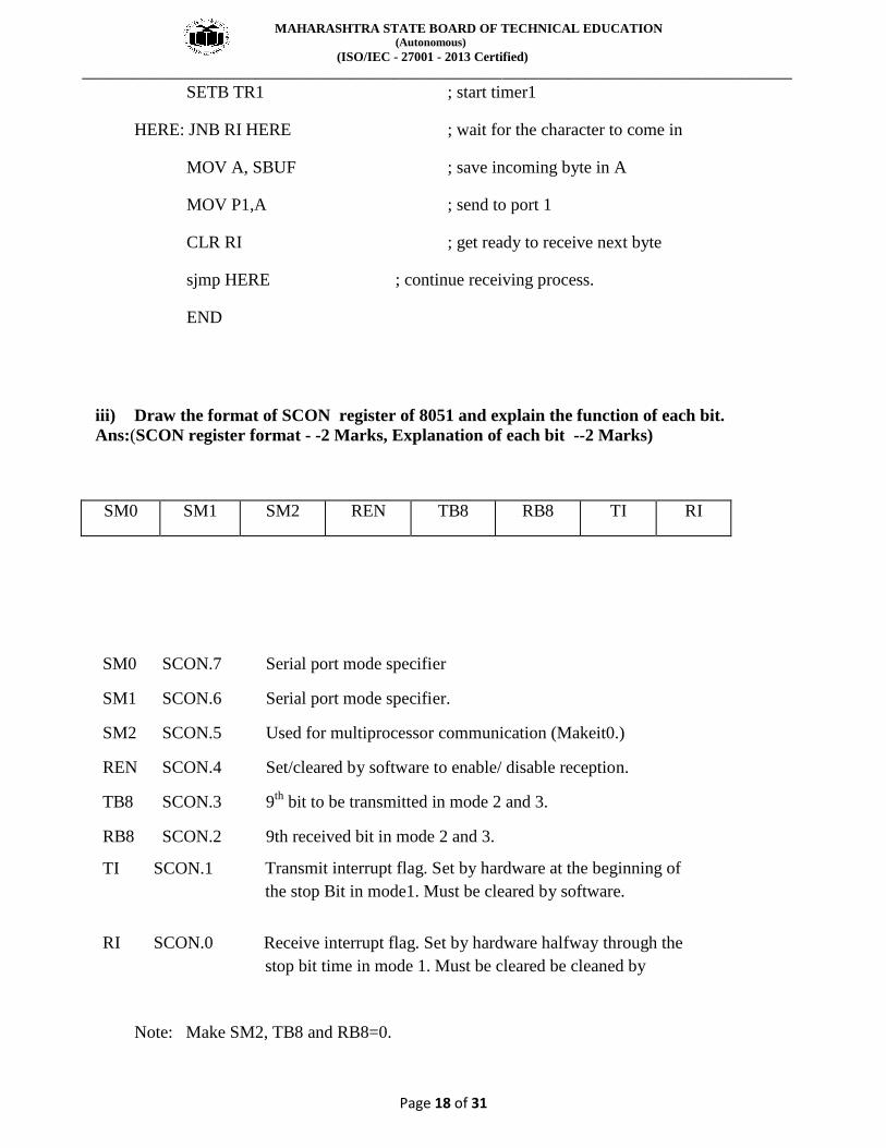
SETB TR1 ; start timer1
HERE: JNB RI HERE ; wait for the character to come in
MOV A, SBUF ; save incoming byte in A
MOV P1,A ; send to port 1
CLR RI ; get ready to receive next byte
sjmp HERE ; continue receiving process.
END
iii) Draw the format of SCON register of 8051 and explain the function of each bit.
Ans:(SCON register format - -2 Marks, Explanation of each bit --2 Marks)
SM0 SM1 SM2 REN TB8 RB8 TI RI
SM0 SCON.7 Serial port mode specifier
SM1 SCON.6 Serial port mode specifier.
SM2 SCON.5 Used for multiprocessor communication (Makeit0.)
REN SCON.4 Set/cleared by software to enable/ disable reception.
TB8 SCON.3 9th
bit to be transmitted in mode 2 and 3.
RB8 SCON.2 9th received bit in mode 2 and 3.
TI SCON.1 Transmit interrupt flag. Set by hardware at the beginning of
the stop Bit in mode1. Must be cleared by software.
RI
SCON.0
Receive interrupt flag. Set by hardware halfway through the
stop bit time in mode 1. Must be cleared be cleaned by
software.
Note: Make SM2, TB8 and RB8=0.
MAHARASHTRA STATE BOARD OF TECHNICAL EDUCATION (Autonomous)
(ISO/IEC - 27001 - 2013 Certified)
__________________________________________________________________________________________________
Page 19 of 31
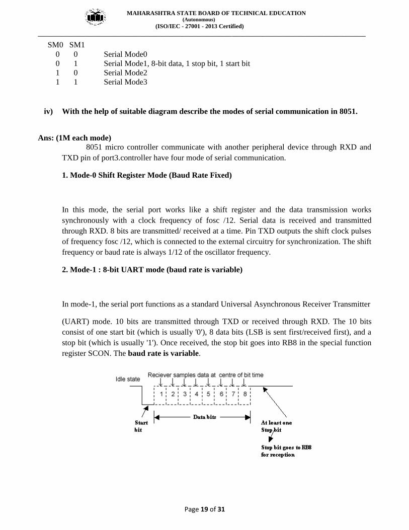
SM0 SM1
0 0 Serial Mode0
0 1 Serial Mode1, 8-bit data, 1 stop bit, 1 start bit
1 0 Serial Mode2
1 1 Serial Mode3
iv) With the help of suitable diagram describe the modes of serial communication in 8051.
Ans: (1M each mode)
8051 micro controller communicate with another peripheral device through RXD and
TXD pin of port3.controller have four mode of serial communication.
1. Mode-0 Shift Register Mode (Baud Rate Fixed)
In this mode, the serial port works like a shift register and the data transmission works
synchronously with a clock frequency of fosc /12. Serial data is received and transmitted
through RXD. 8 bits are transmitted/ received at a time. Pin TXD outputs the shift clock pulses
of frequency fosc /12, which is connected to the external circuitry for synchronization. The shift
frequency or baud rate is always 1/12 of the oscillator frequency.
2. Mode-1 : 8-bit UART mode (baud rate is variable)
In mode-1, the serial port functions as a standard Universal Asynchronous Receiver Transmitter
(UART) mode. 10 bits are transmitted through TXD or received through RXD. The 10 bits
consist of one start bit (which is usually '0'), 8 data bits (LSB is sent first/received first), and a
stop bit (which is usually '1'). Once received, the stop bit goes into RB8 in the special function
register SCON. The baud rate is variable.
MAHARASHTRA STATE BOARD OF TECHNICAL EDUCATION (Autonomous)
(ISO/IEC - 27001 - 2013 Certified)
__________________________________________________________________________________________________
Page 20 of 31
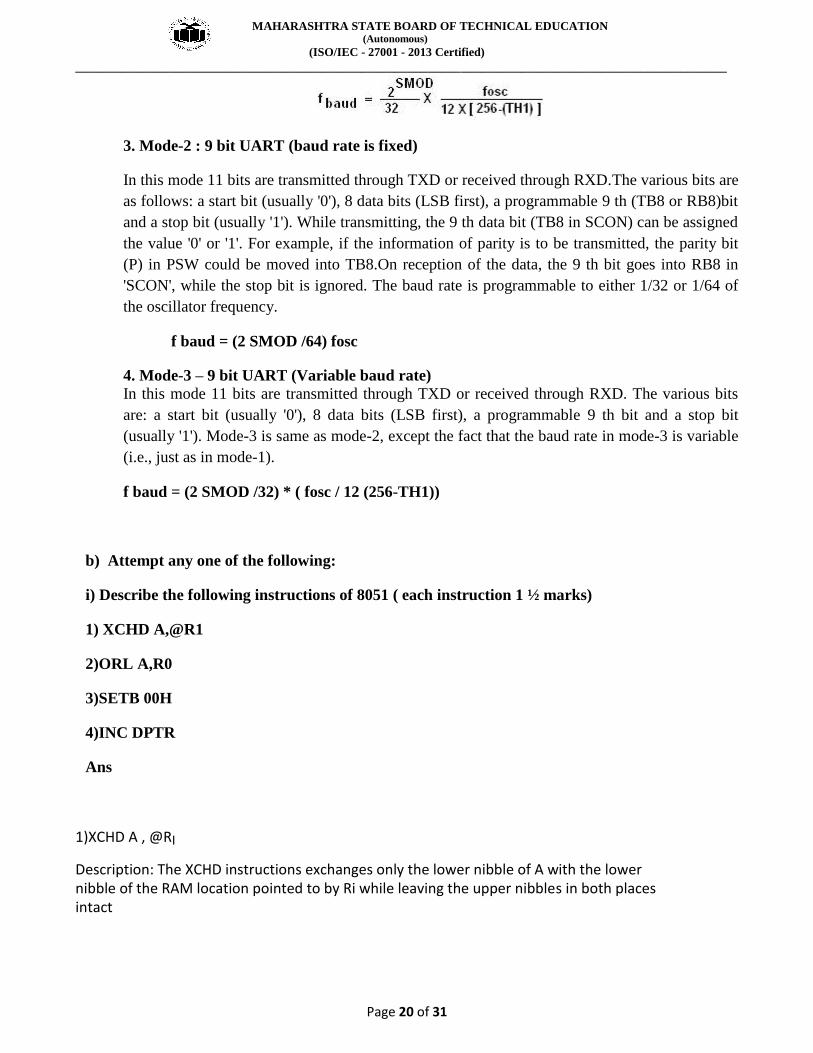
3. Mode-2 : 9 bit UART (baud rate is fixed)
In this mode 11 bits are transmitted through TXD or received through RXD.The various bits are
as follows: a start bit (usually '0'), 8 data bits (LSB first), a programmable 9 th (TB8 or RB8)bit
and a stop bit (usually '1'). While transmitting, the 9 th data bit (TB8 in SCON) can be assigned
the value '0' or '1'. For example, if the information of parity is to be transmitted, the parity bit
(P) in PSW could be moved into TB8.On reception of the data, the 9 th bit goes into RB8 in
'SCON', while the stop bit is ignored. The baud rate is programmable to either 1/32 or 1/64 of
the oscillator frequency.
f baud = (2 SMOD /64) fosc
4. Mode-3 – 9 bit UART (Variable baud rate)
In this mode 11 bits are transmitted through TXD or received through RXD. The various bits
are: a start bit (usually '0'), 8 data bits (LSB first), a programmable 9 th bit and a stop bit
(usually '1'). Mode-3 is same as mode-2, except the fact that the baud rate in mode-3 is variable
(i.e., just as in mode-1).
f baud = (2 SMOD /32) * ( fosc / 12 (256-TH1))
b) Attempt any one of the following:
i) Describe the following instructions of 8051 ( each instruction 1 ½ marks)
1) XCHD A,@R1
2)ORL A,R0
3)SETB 00H
4)INC DPTR
Ans
1)XCHD A , @RI
Description: The XCHD instructions exchanges only the lower nibble of A with the lower nibble of the RAM location pointed to by Ri while leaving the upper nibbles in both places intact
MAHARASHTRA STATE BOARD OF TECHNICAL EDUCATION (Autonomous)
(ISO/IEC - 27001 - 2013 Certified)
__________________________________________________________________________________________________
Page 21 of 31
2) ORL A,R0
Description :OR each bit of A with the same bit of register R0 and result is stored in A.
3) SETB 00H
Description : Set the bit addressable bit i.e 00H to 1
4) INC DPTR
Description :Add a 1 to the 16 bit DPTR register.
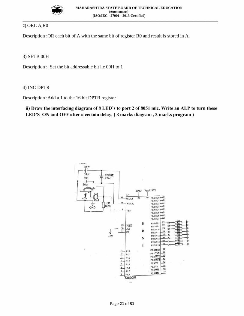
ii) Draw the interfacing diagram of 8 LED’s to port 2 of 8051 mic. Write an ALP to turn these
LED’S ON and OFF after a certain delay. ( 3 marks diagram , 3 marks program )
MAHARASHTRA STATE BOARD OF TECHNICAL EDUCATION (Autonomous)
(ISO/IEC - 27001 - 2013 Certified)
__________________________________________________________________________________________________
Page 22 of 31
Program
Org 0000h
Sjmp start
Org 0030h
Start: MOV SP,#30h
MOV A, # 0FFH ; Store FFH in A
BACK: MOV P2, A ; move FF to P2 to glow all the LEDs
ACALL DELAY : wait for some time
CPL A ; turn off the LEDs
SJMP BACK
DELAY: MOV R3, #255
AGAIN: DJNZ R3, AGAIN
RET
End
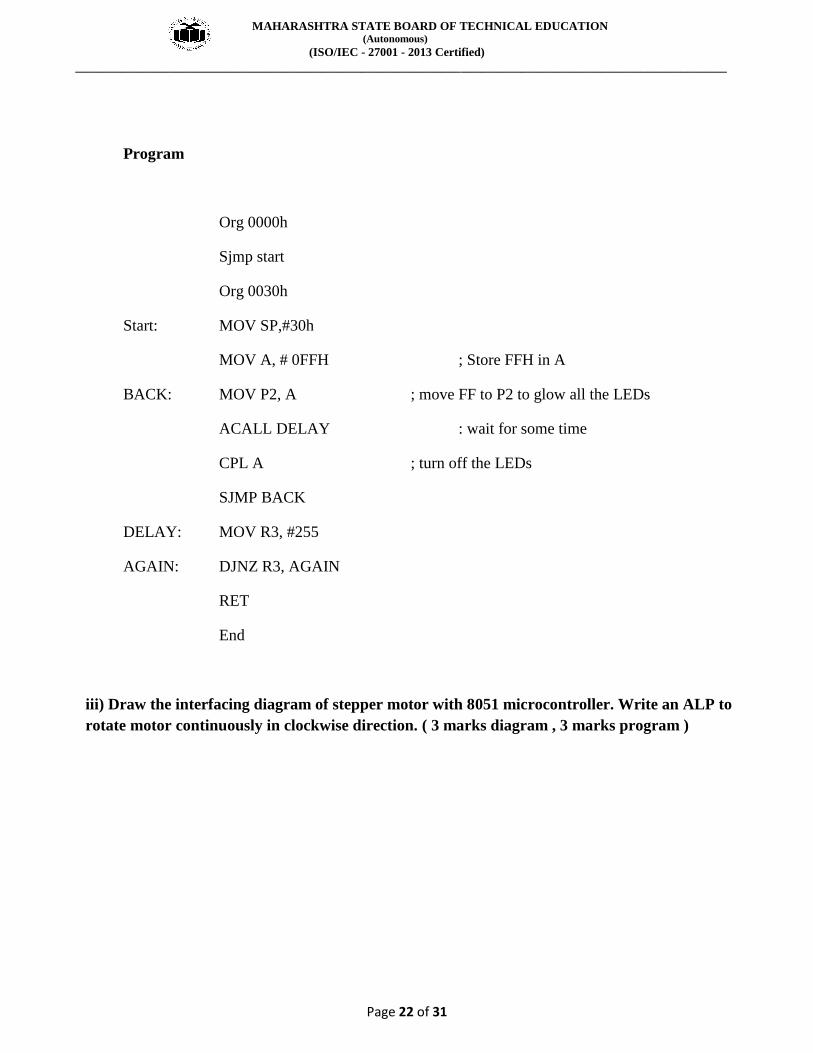
iii) Draw the interfacing diagram of stepper motor with 8051 microcontroller. Write an ALP to
rotate motor continuously in clockwise direction. ( 3 marks diagram , 3 marks program )
MAHARASHTRA STATE BOARD OF TECHNICAL EDUCATION (Autonomous)
(ISO/IEC - 27001 - 2013 Certified)
__________________________________________________________________________________________________
Page 23 of 31
Program
Org 0000h
Sjmp start
Org 0030h
Start: MOV SP,#30h
MOV A,#66H ;load step sequence
BACK: MOV P1,A ;issue sequence to motor
RRA ;rotate right clockwise
ACALL DELAY ;wait
SJMP BACK ;keep going
DELAY: MOV R2,#100
H1: MOV R3,#255
H2: DJNZ R3,H2
DJNZ R2,H1
RET
End
MAHARASHTRA STATE BOARD OF TECHNICAL EDUCATION (Autonomous)
(ISO/IEC - 27001 - 2013 Certified)
__________________________________________________________________________________________________
Page 24 of 31
Or
Org 0000h
Sjmp start
Org 0030h
Start: MOV SP,#30h
AGAIN: MOV R1,#4
BACK: MOV A,#00H
MOV DPTR,#2000h
MOVC A,@A+DPTR
MOV P1,A ;issue sequence to motor
ACALL DELAY ;wait
INC DPTR
DJNZ R1,BACK
SJMP AGAIN ;keep going
DELAY: MOV R2,#100
H1: MOV R3,#255
H2: DJNZ R3,H2
DJNZ R2,H1
RET
EXCIT: db 03h,06h,0ch,09h
End
Q 5. Attempt any four of the following:
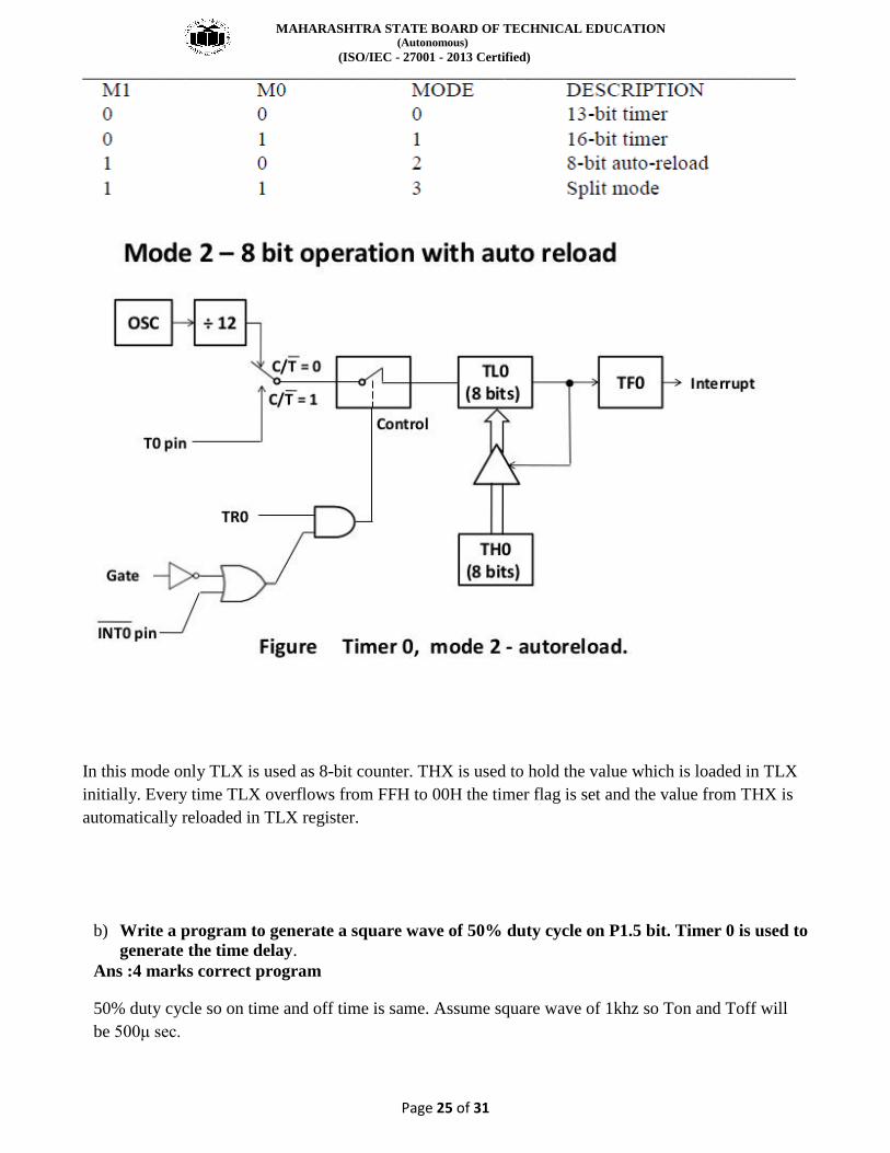
a) State the different timer modes of 8051.Describe mode 2 in detail.( 2 marks modes and 2
marks description of mode-2 )
MAHARASHTRA STATE BOARD OF TECHNICAL EDUCATION (Autonomous)
(ISO/IEC - 27001 - 2013 Certified)
__________________________________________________________________________________________________
Page 25 of 31
In this mode only TLX is used as 8-bit counter. THX is used to hold the value which is loaded in TLX
initially. Every time TLX overflows from FFH to 00H the timer flag is set and the value from THX is
automatically reloaded in TLX register.
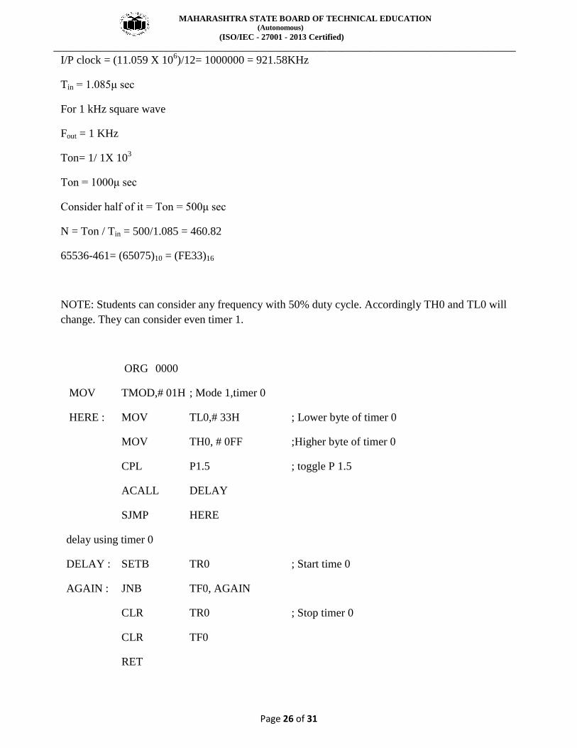
b) Write a program to generate a square wave of 50% duty cycle on P1.5 bit. Timer 0 is used to
generate the time delay.
Ans :4 marks correct program
50% duty cycle so on time and off time is same. Assume square wave of 1khz so Ton and Toff will
be 500μ sec.
MAHARASHTRA STATE BOARD OF TECHNICAL EDUCATION (Autonomous)
(ISO/IEC - 27001 - 2013 Certified)
__________________________________________________________________________________________________
Page 26 of 31
I/P clock = (11.059 X 10⁶)/12= 1000000 = 921.58KHz
Tin = 1.085μ sec
For 1 kHz square wave
Fout = 1 KHz
Ton= 1/ 1X 10³
Ton = 1000μ sec
Consider half of it = Ton = 500μ sec
N = Ton / Tin = 500/1.085 = 460.82
65536-461= (65075)10 = (FE33)16
NOTE: Students can consider any frequency with 50% duty cycle. Accordingly TH0 and TL0 will
change. They can consider even timer 1.
ORG 0000
MOV TMOD,# 01H ; Mode 1,timer 0
HERE : MOV TL0,# 33H ; Lower byte of timer 0
MOV TH0, # 0FF ;Higher byte of timer 0
CPL P1.5 ; toggle P 1.5
ACALL DELAY
SJMP HERE
delay using timer 0
DELAY : SETB TR0 ; Start time 0
AGAIN : JNB TF0, AGAIN
CLR TR0 ; Stop timer 0
CLR TF0
RET
MAHARASHTRA STATE BOARD OF TECHNICAL EDUCATION (Autonomous)
(ISO/IEC - 27001 - 2013 Certified)
__________________________________________________________________________________________________
Page 27 of 31
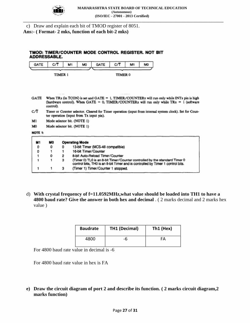
c) Draw and explain each bit of TMOD register of 8051.
Ans:- ( Format- 2 mks, function of each bit-2 mks)
d) With crystal frequency of f=11.0592MHz,what value should be loaded into TH1 to have a
4800 baud rate? Give the answer in both hex and decimal . ( 2 marks decimal and 2 marks hex
value )
Baudrate TH1 (Decimal) Th1 (Hex)
4800 -6 FA
For 4800 baud rate value in decimal is -6
For 4800 baud rate value in hex is FA
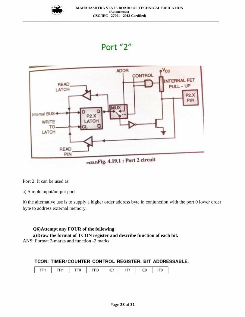
e) Draw the circuit diagram of port 2 and describe its function. ( 2 marks circuit diagram,2
marks function)
MAHARASHTRA STATE BOARD OF TECHNICAL EDUCATION (Autonomous)
(ISO/IEC - 27001 - 2013 Certified)
__________________________________________________________________________________________________
Page 28 of 31
Port 2: It can be used as
a) Simple input/output port
b) the alternative use is to supply a higher order address byte in conjunction with the port 0 lower order
byte to address external memory.
Q6)Attempt any FOUR of the following:
a) Draw the format of TCON register and describe function of each bit.
ANS: Format 2-marks and function -2 marks
MAHARASHTRA STATE BOARD OF TECHNICAL EDUCATION (Autonomous)
(ISO/IEC - 27001 - 2013 Certified)
__________________________________________________________________________________________________
Page 29 of 31
TF1 TCON. 7 Timer 1 overflows flag. Set by hardware when the Timer/Counter 1
Overflows. Cleared by hardware as processor vectors to the interrupt service routine.
TR1TCON. 6 Timer 1 run control bit. Set/cleared by software to turn Timer/Counter 1 ON/OFF.
TF0 TCON. 5 Timer 0 overflow flag. Set by hardware when the Timer/Counter 0 overflows. Cleared
by hardware as processor vectors to the service routine.
TR0 TCON. 4 Timer 0 run control bit. Set/cleared by software to turn Timer/Counter 0 ON/OFF.
IE1 TCON. 3 External Interrupt 1 edge flag. Set by hardware when External Interrupt edge is detected.
Cleared by hardware when interrupt is processed.
IT1 TCON. 2 Interrupt 1 type control bit. Set/cleared by software to specify
falling edge/low level triggered External Interrupt.
IE0 TCON. 1 External Interrupt 0 edge flag. Set by hardware when External
Interrupt edge detected. Cleared by hardware when interrupt is processed.
IT0 TCON. 0 Interrupt 0 type control bit. Set/cleared by software to
Specify falling edge/low level triggered External Interrupt
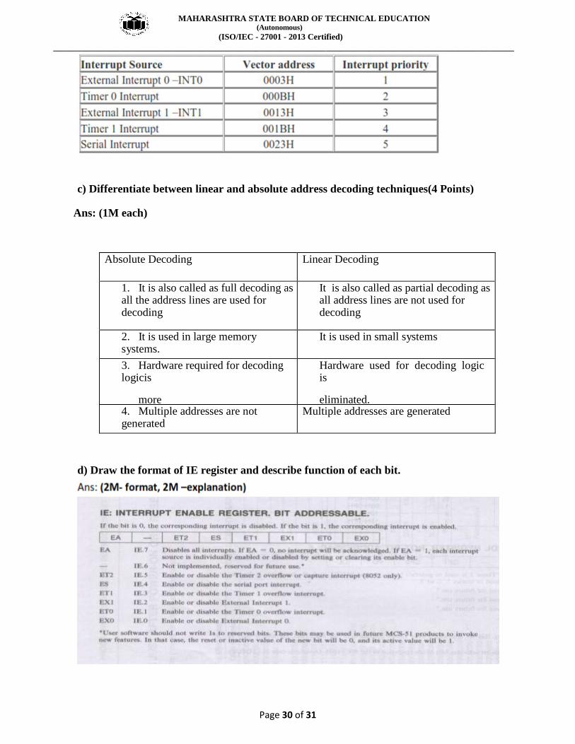
b) State the different types of interrupts in 8051 with their priorities and vector address. Ans:-
(List 2 mks, priorities 1 mks, vector location -1 mks)
MAHARASHTRA STATE BOARD OF TECHNICAL EDUCATION (Autonomous)
(ISO/IEC - 27001 - 2013 Certified)
__________________________________________________________________________________________________
Page 30 of 31
c) Differentiate between linear and absolute address decoding techniques(4 Points)
Ans: (1M each)
Absolute Decoding Linear Decoding
1. It is also called as full decoding as all the address lines are used for decoding
It is also called as partial decoding as all address lines are not used for decoding
2. It is used in large memory systems.
It is used in small systems
3. Hardware required for decoding logicis
more
Hardware used for decoding logic is
eliminated. 4. Multiple addresses are not generated
Multiple addresses are generated
d) Draw the format of IE register and describe function of each bit.
MAHARASHTRA STATE BOARD OF TECHNICAL EDUCATION (Autonomous)
(ISO/IEC - 27001 - 2013 Certified)
__________________________________________________________________________________________________
Page 31 of 31
e) Describe any four factors on which selection of microcontroller depends .( Each factor 1
mark)
Ans: The selection of microcontroller depends upon the type of application. The following factors
must be
considered while selecting the microcontroller.
1. Word length: The word length of microcontroller is either 8, 16 or 32 bit. As the word
length increases, the cost, power dissipation and speed of the microcontroller increases.
2. Power dissipation: It depends upon various factors like clock frequency, speed, supply
voltage, VLSI technology etc. For battery operated embedded systems, we must use low
power microcontrollers.
3. Clock frequency: The speed of an embedded system depends upon the clock frequency.
The clock frequency depends upon the application.
4. Instruction Set: On the basis of instructions microcontrollers are classified into two
categories 1. CISC 2. RISC.
CISC system improves software flexibility. Hence it is used in general purpose
systems.
RISC improves speed of the system for the particular applications.
5. Internal resources: The internal resources are ROM, RAM, EEPROM, FLASH ROM,
UART, TIMER, watch dog timer, PWM, ADC, DAC, network interface, wireless
interface etc. It depends upon the application for which microcontroller is going to be
used.
6. I/O capabilities: The number of I/O ports, size and characteristics of each I/O port, speed
of operation of the I/O port, serial port or parallel ports. These are the considerations
needed to ascertain.


