Embed Size (px)
Citation preview
Old Dominion University Old Dominion University
ODU Digital Commons ODU Digital Commons
Electrical & Computer Engineering Faculty Publications Electrical & Computer Engineering
2021
Logical Modeling of Adiabatic Logic Circuits Using VHDL Logical Modeling of Adiabatic Logic Circuits Using VHDL
Lee Belfore Old Dominion University, [email protected]
Follow this and additional works at: https://digitalcommons.odu.edu/ece_fac_pubs
Part of the Power and Energy Commons, and the VLSI and Circuits, Embedded and Hardware Systems
Commons
Original Publication Citation Original Publication Citation Belfore, L. (2021). Logical modeling of adiabatic logic circuits using VHDL. In Y. Shan, G. Hu, Q. Yan, & T. Goto, Proceedings of ISCA 34th International Conference on Computer Applications in Industry and Engineering (pp. 30-39). EasyChair. https://doi.org/10.29007/6wln
This Conference Paper is brought to you for free and open access by the Electrical & Computer Engineering at ODU Digital Commons. It has been accepted for inclusion in Electrical & Computer Engineering Faculty Publications by an authorized administrator of ODU Digital Commons. For more information, please contact [email protected].
EPiC Series in ComputingVolume 79, 2021, Pages 30–39
Proceedings of ISCA 34th International Conference onComputer Applications in Industry and Engineering
Logical Modeling of Adiabatic Logic Circuits using VHDLLee A. Belfore II
Old Dominion University, Norfolk, Virginia, [email protected]
Abstract
The underlying nature of adiabatic circuits is most accurately characterized at the circuit level asit is for traditional technologies. In order to scale system designs for adiabatic logic technologies,modeling of adiabatic circuits at the logic level is necessary. Logic level models of adiabatic logiccircuits can facilitate the design, development, and verification of large scale digital systems that maybe infeasible using circuit simulators. Adiabatic logic circuits can be powered with a four stage powerclock consisting of idle, charge, hold, and recover stages that provides for adiabatic charging andcharge recovery to give adiabatic circuits their low power operation. By both discretizing the temporalaspects of the power clock and the logic values, a logical model of adiabatic circuit operation isproposed. Using the expressive capabilities of Very High Speed Integrated Circuit (VHSIC) HardwareDescription Language (VHDL), the salient aspects of adiabatic circuit models can be captured. In thiswork, a VHDL framework is defined for modeling adiabatic logic circuits & systems and its use isdemonstrated in several example adiabatic logic circuits.
1 IntroductionAdiabatic logic circuit technology offers lower power consumption compared with CMOS
technologies by energizing circuits adiabatically energized and then adiabatically recovering storedenergy from the circuit for later use [7, 3, 8, 10]. The efficiency and behavior is established by thecircuit level behaviors that are quantified in circuit simulations and measured in actual circuits. Once thecircuits are suitably characterized, the overall operation can be described symbolically. This descriptionof their operation is the basis for logical models of adiabatic circuits.
With current digital system design requirements and modeling practices, it is impractical to relysolely on circuit simulations to validate a design because the circuit simulations require substantialcomputational resources. As a result, the design process employs conservative models with conservativemargins, including reduced fidelity, to enable the verification of circuit operation while substituting highfidelity circuit level models for vetted approximation methodologies or limiting circuit simulation tospecial cases requiring circuit level fidelity. The fidelity is not reduced in an arbitrary fashion, but ratheraspects of the circuit operation are modeled symbolically. Circuit level properties associated with thesymbolic representations can be included using a circuit extraction step to improve the fidelity of themodel. Such is what is done with circuit delays, for example.
Approaches for modeling adiabatic and partially adiabatic circuits appear in the literature [11, 12].In Varga et al., the adiabatic pipeline is modeled using the IEEE std_logic type for logic values andguarded blocks to manifest the timing of the power clock [11]. The motivation is to model the pipeline
Y. Shi, G. Hu, Q. Yuan and T. Goto (eds.), CAINE 2021 (EPiC Series in Computing, vol. 79), pp. 30–39
Adiabatic Modeling using VHDL Belfore
structure in anticipation of synthesis. Finally, approaches for modeling in Verilog are developed [12]with the observation that VHDL is similarly capable. The clear intent of these approaches is to facilitatemodeling larger scale models and facilitate synthesis based on the logical behavior of the models.
More generally in the literature, adiabatic circuit dynamics can be modeled with VHDL by one oftwo methods. First, VHDL libraries can be created with the specific capacity to model analog signals[9]. In addition, the VHDL standard has been extended to support mixed analog/digital modeling inVHDL-AMS [1]. In both of these approaches, the circuit is ultimately represented by a system ofdifferential equations. In these works, it would be necessary to develop libraries to support adiabaticcircuit models. The principle disadvantage in these approaches is the significant simulation time forlarge circuits. During development, it is more pragmatic to focus on logical modeling, constrained byconservative performance metrics, to facilitate iterative design. Once the design approaches the finalphase, then it may become necessary to shift to higher fidelity circuit simulations.
In this work, an approach is introduced for modeling adiabatic circuits. The model defines amultivalued logic value definition consistent with adiabatic circuit operating modes. The logic valuesfacilitate developing adiabatic logic pipelines and troubleshooting of logic circuits. Importantly, themodel preserves the dual rail nature of adiabatic signals.
This paper is organized into five sections including an introduction, an overview of the operation ofadiabatic circuits, a presentation of adiabatic VHDL models, simulation results for several examples,and a summary.
2 Adiabatic Logic Circuits OperationIn this section, a logical model for adiabatic circuit operation is presented. The intention is to create
a symbolic representation of adiabatic circuit operation and not model actual circuit level behaviors.The interested reader can find the details of adiabatic circuit operation elsewhere [7, 3, 8, 10, 2].
Adiabatic circuit operation is both powered and coordinated by the power clock. The power clock isa periodic signal that powers circuits performing logic operations, hold the values for a sufficient timeto propagate logic values to the next layer of logic, and then recovers as much energy from the circuitto be recycled for future operations. From a logical modeling perspective, the power clock discretizestime.
The power clock is structured into four segments reflecting the different stages adiabatic circuitoperation. In this paper, the segments will be designated as Charge (C), Hold (H), Recover (R), and Idle(I). The first segment is the charge segment (often also called the evaluate). During the charge segment,the circuit is adiabatically energized by gradually increasing the power clock voltage while its inputsare held constant. At the end of the charge segment, the circuit is fully energized with the outputs atfull scale presenting the result of the gate’s logic function. During the hold segment, the power clockis constant, holding the outputs constant for the duration of next layer of logic’s charge segment. In therecover segment, the power clock voltage is gradually reduced while at concurrently, through the powerclock line, adiabatically recovering charge from the circuit. Finally, in the idle stage, the circuit is notenergized and the power clock is at its minimum. Further, the duration of the idle segment depends onthe number of power clock phases.
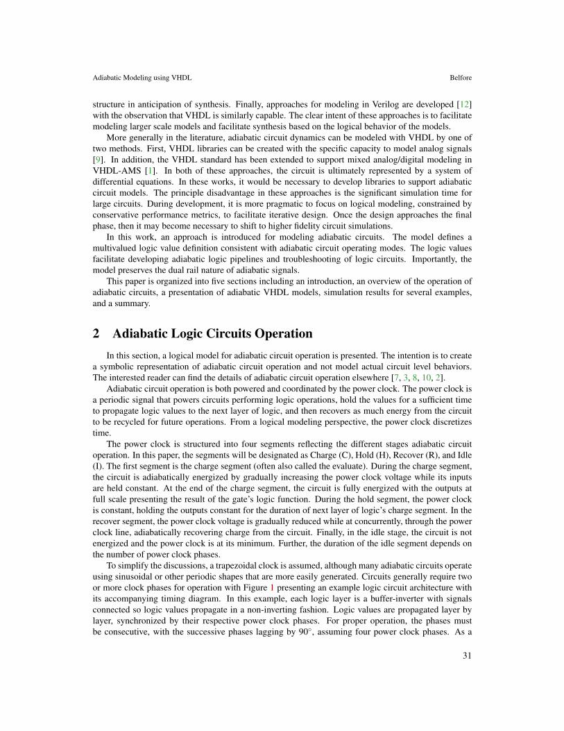
To simplify the discussions, a trapezoidal clock is assumed, although many adiabatic circuits operateusing sinusoidal or other periodic shapes that are more easily generated. Circuits generally require twoor more clock phases for operation with Figure 1 presenting an example logic circuit architecture withits accompanying timing diagram. In this example, each logic layer is a buffer-inverter with signalsconnected so logic values propagate in a non-inverting fashion. Logic values are propagated layer bylayer, synchronized by their respective power clock phases. For proper operation, the phases mustbe consecutive, with the successive phases lagging by 90◦, assuming four power clock phases. As a
31
Adiabatic Modeling using VHDL Belfore
consequence of the power clocks organization, layers of logic form a pipeline of sorts, each poweredby the successive power clock phase. In Figure 1, the input that is applied alternates '1's and '0's onsuccessive power clock cycles.
Layer 3
Layer 2
Layer 1
φ1
φ2
φ3
φ4
Layer 4
Inputs Outputs
Power ClockPhases
(a) Circuit architecture
A
A
φ4
φ3
φ2
φ1
F
F
Z
Z
Y
Y
X
X
(b) Buffer-inverter chain
φ1
φ2
φ3
φ4
t0
t1
t2
t3
t4
t5
t6
t7
t8
t9
t10
t11
C I
R
IC
I
C
C C
C
C
C
I
II I
I
I
I II
I
H H H
HHH
H H H H
HHH
R R
R R R R
R R R C
R R RC C C C
X
Y
Z
A
’1’ ’0’ ’1’
’1’’0’’1’
’1’ ’0’ ’1’
’1’’0’’1’
’1’ ’0’ ’1’
F
(c) Timing diagram for buffer-inverter chain.
Figure 1: Adiabatic circuit operation.
3 Adiabatic VHDL ModelsRefining the ideas introduced in §2, VHDL models for adiabatic circuits are presented here. Recall,
hardware description languages (HDLs) are programming languages that model complex digital systemsand serve as the source for hardware synthesis. HDLs facilitate specification of digital systems bymodeling systems logically rather than at the circuit level. In addition, HDLs include familiar high-levellanguage (HLL) programming capabilities for computing static constants, to support system modeling,and to create desired modeling capabilities. For adiabatic logic circuits modeled at a temporal resolutionwhere the influence of the power clock is important, the HLL features will be used to implement thelogical behaviors of adiabatic logic circuits.
3.1 Anatomy of a VHDL ModelA VHDL model consists of an entity and an architecture [5]. The entity defines the model interface
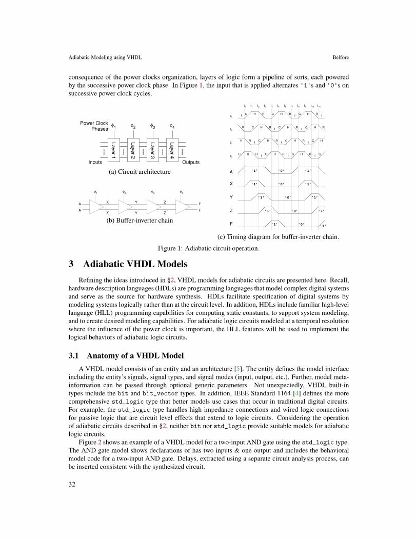
including the entity’s signals, signal types, and signal modes (input, output, etc.). Further, model meta-information can be passed through optional generic parameters. Not unexpectedly, VHDL built-intypes include the bit and bit_vector types. In addition, IEEE Standard 1164 [4] defines the morecomprehensive std_logic type that better models use cases that occur in traditional digital circuits.For example, the std_logic type handles high impedance connections and wired logic connectionsfor passive logic that are circuit level effects that extend to logic circuits. Considering the operationof adiabatic circuits described in §2, neither bit nor std_logic provide suitable models for adiabaticlogic circuits.
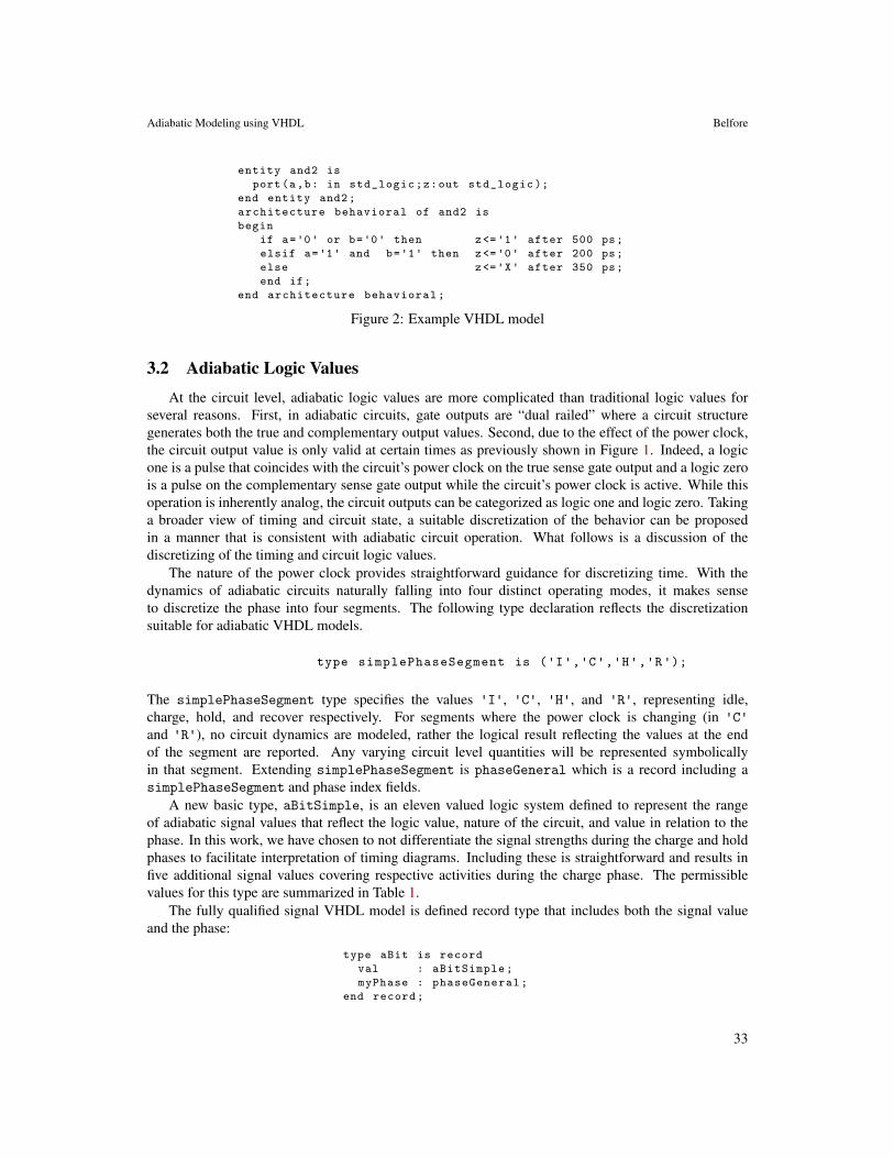
Figure 2 shows an example of a VHDL model for a two-input AND gate using the std_logic type.The AND gate model shows declarations of has two inputs & one output and includes the behavioralmodel code for a two-input AND gate. Delays, extracted using a separate circuit analysis process, canbe inserted consistent with the synthesized circuit.
32
I I 'j-----tl ----+-+-t-----f
Adiabatic Modeling using VHDL Belfore
entity and2 is
port(a,b: in std_logic;z:out std_logic );
end entity and2;
architecture behavioral of and2 is
begin
if a='0' or b='0' then z<='1' after 500 ps;
elsif a='1' and b='1' then z<='0' after 200 ps;
else z<='X' after 350 ps;
end if;
end architecture behavioral;
Figure 2: Example VHDL model
3.2 Adiabatic Logic Values
At the circuit level, adiabatic logic values are more complicated than traditional logic values forseveral reasons. First, in adiabatic circuits, gate outputs are “dual railed” where a circuit structuregenerates both the true and complementary output values. Second, due to the effect of the power clock,the circuit output value is only valid at certain times as previously shown in Figure 1. Indeed, a logicone is a pulse that coincides with the circuit’s power clock on the true sense gate output and a logic zerois a pulse on the complementary sense gate output while the circuit’s power clock is active. While thisoperation is inherently analog, the circuit outputs can be categorized as logic one and logic zero. Takinga broader view of timing and circuit state, a suitable discretization of the behavior can be proposedin a manner that is consistent with adiabatic circuit operation. What follows is a discussion of thediscretizing of the timing and circuit logic values.
The nature of the power clock provides straightforward guidance for discretizing time. With thedynamics of adiabatic circuits naturally falling into four distinct operating modes, it makes senseto discretize the phase into four segments. The following type declaration reflects the discretizationsuitable for adiabatic VHDL models.
type simplePhaseSegment is ('I','C','H','R');
The simplePhaseSegment type specifies the values 'I', 'C', 'H', and 'R', representing idle,charge, hold, and recover respectively. For segments where the power clock is changing (in 'C'and 'R'), no circuit dynamics are modeled, rather the logical result reflecting the values at the endof the segment are reported. Any varying circuit level quantities will be represented symbolicallyin that segment. Extending simplePhaseSegment is phaseGeneral which is a record including asimplePhaseSegment and phase index fields.
A new basic type, aBitSimple, is an eleven valued logic system defined to represent the rangeof adiabatic signal values that reflect the logic value, nature of the circuit, and value in relation to thephase. In this work, we have chosen to not differentiate the signal strengths during the charge and holdphases to facilitate interpretation of timing diagrams. Including these is straightforward and results infive additional signal values covering respective activities during the charge phase. The permissiblevalues for this type are summarized in Table 1.
The fully qualified signal VHDL model is defined record type that includes both the signal valueand the phase:
type aBit is record
val : aBitSimple;
myPhase : phaseGeneral;
end record;
33

Adiabatic Modeling using VHDL Belfore
Table 1: Summary of Adiabatic Signal Values for the aBitSimple type
Value Description'U' driving uninitialized value'X' driving unknown value'0' driving logic zero'1' driving logic one'Z' high impedance'u' recovery uninitialized value'x' recovery unknown value'L' recovery logic zero'H' recovery logic one'z' recovery high impedance'*' fully discharged
Including the phase in the signal definition enables run time checking to confirm the aBit phase isconsistent with the assigned phase of the gate’s power clock.
Several utility routines have been created to help manage signal values and phases. Some routinesfacilitate the conversion between standard signal types (bit and std_logic) and the new aBit type.Furthermore, operator overloading for the new logic type has been implemented to permit the naturalcomposition of logic expressions. In the event indeterminate inputs or phase errors occur, the logicoperations evaluate to an unknown value to facilitate troubleshooting. Finally, the logic values 'Z' and'z', along with the requisite bus resolution functions, permit high impedance bus modeling.
3.3 Logical Adiabatic Gate ModelThe logical adiabatic gate model requires changes both to the gate entity and to the behavior defined
in its architecture. The adiabatic gates perform logic functions, so one reasonable approach wouldbe to adopt traditional logic values in the gate model. In this approach, phase information would belost. Furthermore, adiabatic gates are dual rail, whose representation not as important as the powerclock phase in logical modeling, their explicit inclusion provides an opportunity to have visibility forall signals in the circuit. Apropos, the entity for the AND gate shown in Figure 3 will require dual railinput & output logic signals and the clock phase driving the gate.
entity adbAnd2 is
port(
phi : in generalPhase;
a,an: in aBit;
b,bn: in aBit;
z,zn:out aBit
);
end entity adbAnd2;
Figure 3: Entity for two-input adiabatic AND gate
Determining the gate outputs is no longer a simple matter of evaluating the gate’s logic functionbased in the circuit inputs because of the dependence on the power clock segment. The model presentedin Figure 4 implements the behavior for the two-input adiabatic AND gate that accounts for the powerclock. When the clock phase changes, input phase segments are verified to be the same and also one
34
Adiabatic Modeling using VHDL Belfore
segment preceding the gate’s power clock phase segment where the output value is determined in thecharge segment. A phase error results in the output signal being assigned an 'X' value. Since logicaloperations have been overloaded, the gate logic function is expressed in a natural fashion, permittinglogic equations to model the respective MOS switching networks. Logic operations are evaluated intheir respective common phase, facilitating the composition of complex logic functions. The resultingvalue is stored in a temporary variable so that the phase can be correctly updated to be consistent withthe power clock for the gate. In transitioning to and during the hold segment, the logic gate outputsremain constant in the model.
process(phi)
variable zInt ,znInt:aBit;
begin
-- check for valid input and output
-- phase segments
if(isCharging(phi)) then
zInt <= a AND b;
zIntn <= an OR bn;
elsif isHolding(phi) then
-- by VHDL semantics ,
-- no update -no signal change
elsif isRecovering(phi) then
zInt := deenergize(zInt);
znInt := deenergize(znInt);
else -- idle
zInt.val := '*';znInt.val := '*';
end if;
assignToPhase(zInt , phi);
assignToPhase(znInt , phi);
z <= zInt;
zn <= znInt;
end process;
Figure 4: Behavioral model for two-input adiabatic AND gate
Table 2: Utility functions and Procedures
Name PurposeisCharging function, returns true when power clock is chargingisHolding function, returns true when power clock is maximalisRecovering function, returns true when power clock is dischargingisIdle function, returns true when power clock is offdeenergize procedure, reduces the strength of signal while retaining logic valueassignToPhase procedure, assigns a phase to a signal
3.4 Extending to Other Logic GatesThe dual rail nature of the logic gates simplifies creating families of logic gates. Signal inversion
is accomplished simply by swapping the true and complementary signal rails requiring no additionalcircuitry. Indeed, with DeMorgan’s Theorem, it is easy to show that by swapping dual rail signals tocomplement inputs & outputs, the two-input AND gate can also serve as an OR, NAND, or NOR gate.
35
Adiabatic Modeling using VHDL Belfore
In addition, more complex logic functions can be modeled using the logic equation for the true inputvalues and the dual logic equation for the complementary input values.
For example, the logic equations for a full adder are
S = A⊕B⊕CiCo = A ·B+A ·Ci +B ·Ci
(1)
With traditional CMOS logic, the full adder can be implemented with several gates. In adiabaticlogic, each logic function can be implemented with a MOS switching network, so the full adder can beimplemented with two adiabatic logic gates. The logic equations for the complementary networks are
S = A⊕B⊕CiCo = (A+B) · (A+Ci) · (B+Ci)
(2)
The second example is a multiplexer with dedicated, mutually exclusive select lines. The generaltrue and complementary logic equations are
Z =N−1
∑i=0
SiDi Z =N−1
∏i=0
(Si +Di), (3)
where N is the number of data inputs. It is also easy to show that, for N = 2, (3) can specify two-inputXOR and XNOR gates.
3.5 Test Bench
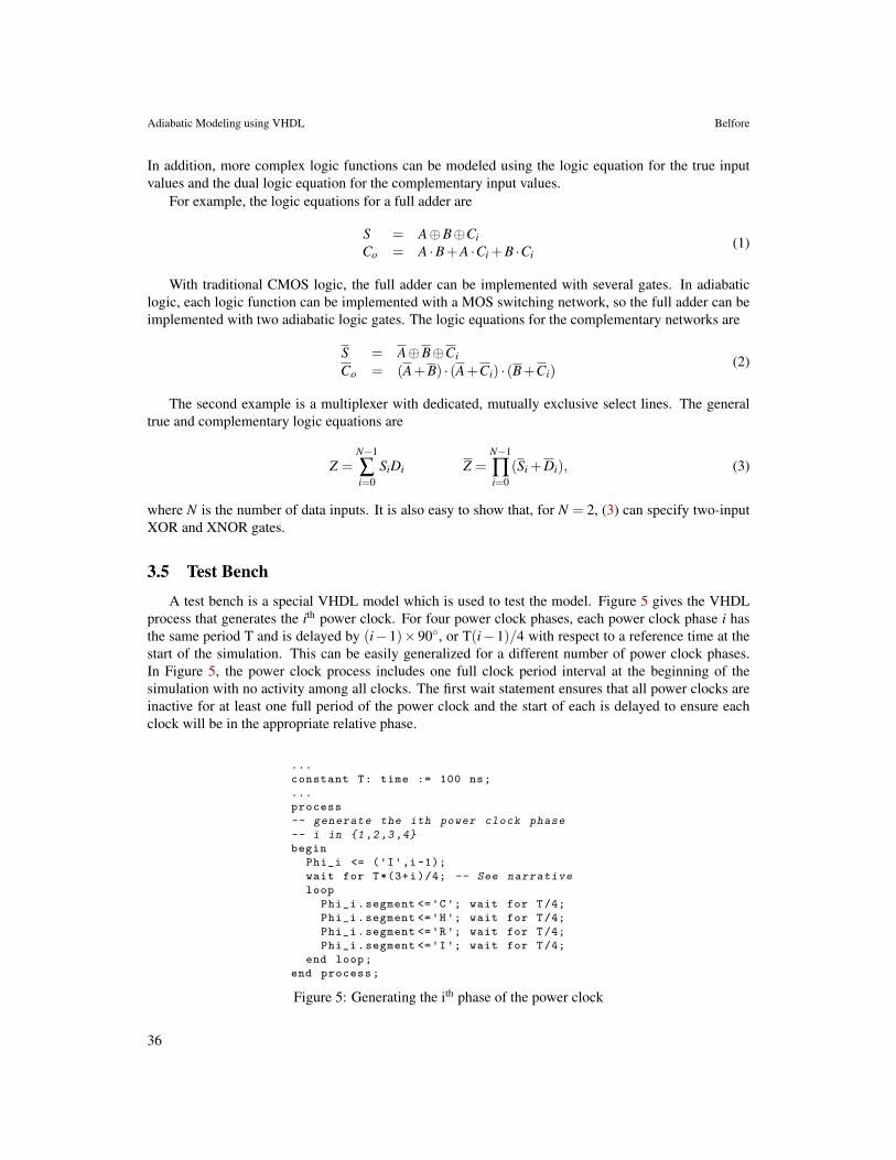
A test bench is a special VHDL model which is used to test the model. Figure 5 gives the VHDLprocess that generates the ith power clock. For four power clock phases, each power clock phase i hasthe same period T and is delayed by (i−1)×90◦, or T(i−1)/4 with respect to a reference time at thestart of the simulation. This can be easily generalized for a different number of power clock phases.In Figure 5, the power clock process includes one full clock period interval at the beginning of thesimulation with no activity among all clocks. The first wait statement ensures that all power clocks areinactive for at least one full period of the power clock and the start of each is delayed to ensure eachclock will be in the appropriate relative phase.
...
constant T: time := 100 ns;
...
process
-- generate the ith power clock phase
-- i in {1,2,3,4}
begin
Phi_i <= ('I',i-1);wait for T*(3+i)/4; -- See narrative
loop
Phi_i.segment <='C'; wait for T/4;
Phi_i.segment <='H'; wait for T/4;
Phi_i.segment <='R'; wait for T/4;
Phi_i.segment <='I'; wait for T/4;
end loop;
end process;
Figure 5: Generating the ith phase of the power clock
36
Adiabatic Modeling using VHDL Belfore
In order for outputs to conform to proper adiabatic operation, inputs must be set in the appropriatemanner to ensure the adiabatic operation of the gate receiving the input. In addition, it is possible thatdifferent inputs may be required at different logic layers, hence must be synchronized to different powerclock phases. This can be accommodated in one of two ways. First, the inputs can be provided at thesame time and always on the same phase. In this case, buffers will need to be inserted to delay thesignal until it has the required phase for its respective input layer. Second, the inputs can be providedand synchronized to the required phase. The modeling presented works for either method.
4 ExamplesTwo examples of adiabatic logic circuit models are presented here. In the first, a full adder model
is presented. In the second, a Kogge-Stone adder model is presented. The models were verified usingGHDL Version 0.33 under the IEEE-1164 1993 release of the VHDL standard on Ubuntu 16.04. Inaddition, while the modeling is based on the 1993 standard, no issues are anticipated for later VHDLstandard releases. Waveforms are displayed using the GTKWave V3.3 waveform viewer.
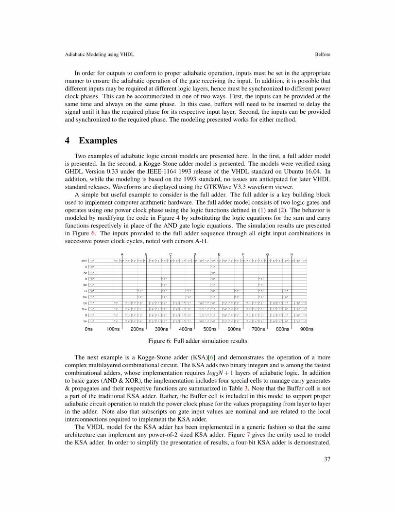
A simple but useful example to consider is the full adder. The full adder is a key building blockused to implement computer arithmetic hardware. The full adder model consists of two logic gates andoperates using one power clock phase using the logic functions defined in (1) and (2). The behavior ismodeled by modifying the code in Figure 4 by substituting the logic equations for the sum and carryfunctions respectively in place of the AND gate logic equations. The simulation results are presentedin Figure 6. The inputs provided to the full adder sequence through all eight input combinations insuccessive power clock cycles, noted with cursors A-H.
0ns 100ns 200ns 300ns 400ns 500ns 600ns 700ns 800ns 900ns
phi1 ’I’ ’C’ ’H’ ’R’ ’I’ ’C’ ’H’ ’R’ ’I’ ’C’ ’H’ ’R’ ’I’ ’C’ ’H’ ’R’ ’I’ ’C’ ’H’ ’R’ ’I’ ’C’ ’H’ ’R’ ’I’ ’C’ ’H’ ’R’ ’I’ ’C’ ’H’ ’R’ ’I’
A ’0’ ’1’
An ’1’ ’0’
B ’0’ ’1’ ’0’ ’1’
Bn ’1’ ’0’ ’1’ ’0’
Ci ’0’ ’1’ ’0’ ’1’ ’0’ ’1’ ’0’ ’1’
Cin ’1’ ’0’ ’1’ ’0’ ’1’ ’0’ ’1’ ’0’
Co ’*’ ’0’ ’L’ ’*’ ’0’ ’L’ ’*’ ’0’ ’L’ ’*’ ’1’ ’H’ ’*’ ’0’ ’L’ ’*’ ’1’ ’H’ ’*’ ’1’ ’H’ ’*’ ’1’ ’H’ ’*’
Con ’*’ ’1’ ’H’ ’*’ ’1’ ’H’ ’*’ ’1’ ’H’ ’*’ ’0’ ’L’ ’*’ ’1’ ’H’ ’*’ ’0’ ’L’ ’*’ ’0’ ’L’ ’*’ ’0’ ’L’ ’*’
S ’*’ ’0’ ’L’ ’*’ ’1’ ’H’ ’*’ ’1’ ’H’ ’*’ ’0’ ’L’ ’*’ ’1’ ’H’ ’*’ ’0’ ’L’ ’*’ ’0’ ’L’ ’*’ ’1’ ’H’ ’*’
Sn ’*’ ’1’ ’H’ ’*’ ’0’ ’L’ ’*’ ’0’ ’L’ ’*’ ’1’ ’H’ ’*’ ’0’ ’L’ ’*’ ’1’ ’H’ ’*’ ’1’ ’H’ ’*’ ’0’ ’L’ ’*’
A B C D E F G H
Figure 6: Full adder simulation results
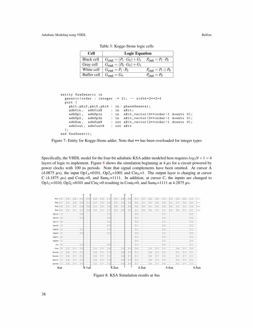
The next example is a Kogge-Stone adder (KSA)[6] and demonstrates the operation of a morecomplex multilayered combinational circuit. The KSA adds two binary integers and is among the fastestcombinational adders, whose implementation requires log2N + 1 layers of adiabatic logic. In additionto basic gates (AND & XOR), the implementation includes four special cells to manage carry generates& propagates and their respective functions are summarized in Table 3. Note that the Buffer cell is nota part of the traditional KSA adder. Rather, the Buffer cell is included in this model to support properadiabatic circuit operation to match the power clock phase for the values propagating from layer to layerin the adder. Note also that subscripts on gate input values are nominal and are related to the localinterconnections required to implement the KSA adder.
The VHDL model for the KSA adder has been implemented in a generic fashion so that the samearchitecture can implement any power-of-2 sized KSA adder. Figure 7 gives the entity used to modelthe KSA adder. In order to simplify the presentation of results, a four-bit KSA adder is demonstrated.
37
Adiabatic Modeling using VHDL Belfore
Table 3: Kogge-Stone logic cells
Cell Logic EquationBlack cell Gout = (P1 ·G0)+G1 Pout = P1 ·P0Gray cell Gout = (P0 ·G0)+G1White cell Gout = P1 ·P0 Pout = P1 ⊕P0Buffer cell Gout = G0 Pout = P0
entity KsaGeneric is
generic(order : integer := 2); -- width =2**2=4
port (
phi1 ,phi2 ,phi3 ,phi4 : in phaseGeneral;
adbCin , adbCinN : in aBit;
adbOp1 , adbOp1n : in aBit_vector (2** order -1 downto 0);
adbOp2 , adbOp2n : in aBit_vector (2** order -1 downto 0);
adbSum , adbSumN : out aBit_vector (2** order -1 downto 0);
adbCout , adbCoutN : out aBit
);
end KsaGeneric;
Figure 7: Entity for Kogge-Stone adder. Note that ** has been overloaded for integer types
Specifically, the VHDL model for the four-bit adiabatic KSA adder modeled here requires log2N+1= 4layers of logic to implement. Figure 8 shows the simulation beginning at 4 µs for a circuit powered bypower clocks with 100 ns periods. Note that signal complements have been omitted. At cursor A(4.0875 µs), the input Op1A=0101, Op2A=1001 and CinA=1. The output layer is charging at cursorC (4.1875 µs) and CoutC=0, and SumC=1111. In addition, at cursor C, the inputs are changed toOp1C=1010, Op2C=0101 and CinC=0 resulting in CoutF=0, and SumF=1111 at 4.2875 µs.
4us 4.1us 4.2us 4.3us 4.4us 4.5us
Phi1 ’C’ ’H’ ’R’ ’I’ ’C’ ’H’ ’R’ ’I’ ’C’ ’H’ ’R’ ’I’ ’C’ ’H’ ’R’ ’I’ ’C’ ’H’ ’R’ ’I’ ’C’
Phi2 ’I’ ’C’ ’H’ ’R’ ’I’ ’C’ ’H’ ’R’ ’I’ ’C’ ’H’ ’R’ ’I’ ’C’ ’H’ ’R’ ’I’ ’C’ ’H’ ’R’ ’I’
Phi3 ’R’ ’I’ ’C’ ’H’ ’R’ ’I’ ’C’ ’H’ ’R’ ’I’ ’C’ ’H’ ’R’ ’I’ ’C’ ’H’ ’R’ ’I’ ’C’ ’H’ ’R’
Phi4 ’H’ ’R’ ’I’ ’C’ ’H’ ’R’ ’I’ ’C’ ’H’ ’R’ ’I’ ’C’ ’H’ ’R’ ’I’ ’C’ ’H’ ’R’ ’I’ ’C’ ’H’
Op1(3) ’1’ ’0’ ’1’ ’0’ ’1’ ’0’
Op1(2) ’0’ ’1’ ’0’ ’1’ ’0’ ’1’
Op1(1) ’0’ ’1’ ’0’ ’1’ ’0’
Op1(0) ’1’ ’0’ ’1’ ’0’ ’1’
Op2(3) ’0’ ’1’ ’0’ ’1’ ’0’ ’1’
Op2(2) ’1’ ’0’ ’1’ ’0’ ’1’ ’0’
Op2(1) ’0’ ’1’ ’0’ ’1’
Op2(0) ’1’ ’0’ ’1’ ’0’
Cin ’0’ ’1’ ’0’ ’1’ ’0’ ’1’
Cout ’0’ ’L’ ’*’ ’0’ ’L’ ’*’ ’0’ ’L’ ’*’ ’0’ ’L’ ’*’ ’1’ ’H’ ’*’ ’0’
Sum(3) ’1’ ’H’ ’*’ ’1’ ’H’ ’*’ ’1’ ’H’ ’*’ ’1’ ’H’ ’*’ ’0’ ’L’ ’*’ ’1’
Sum(2) ’1’ ’H’ ’*’ ’1’ ’H’ ’*’ ’1’ ’H’ ’*’ ’1’ ’H’ ’*’ ’0’ ’L’ ’*’ ’1’
Sum(1) ’1’ ’H’ ’*’ ’1’ ’H’ ’*’ ’1’ ’H’ ’*’ ’1’ ’H’ ’*’ ’0’ ’L’ ’*’ ’1’
Sum(0) ’1’ ’H’ ’*’ ’0’ ’L’ ’*’ ’1’ ’H’ ’*’ ’1’ ’H’ ’*’ ’0’ ’L’ ’*’ ’1’
A B C D E
Figure 8: KSA Simulation results at 4us
38
I I I I I I
I I I I
I I I I I I
I I I I I I
I
I I I I I I
I
I I I I I I
I
I I I I
Adiabatic Modeling using VHDL Belfore
5 Summary and Future WorkA modeling framework has been presented that is consistent with the logical operation of adiabatic
logic circuits. A new type, aBit, was defined that captures the main modes of operation for adiabaticcircuits. The type models the principle adiabatic signal features and ties the operation of the logiccircuits to the power clock. The framework for defining logic functions was presented. Finally, threeexamples simulation results were presented for a full adder and a Kogge-Stone adder.
Future work will include verifying the operation of the modeling framework on a wider variety ofadiabatic and reversible circuits. In addition, applicability to different clocking schemes & timing andenergy modeling will be investigated as well.
References[1] Ernst Christen and Kenneth Bakalar. VHDL-AMS – a hardware description language for analog and mixed-
signal applications. IEEE Transactions on Circuits and Systems–II Analog and Digital Signal Processing,46(10):1263–1272, October 1999.
[2] Mihail Cutitaru. IDPAL A Partially-Adiabatic Energy-Efficient Logic Family: Theory and Applications toSecure Computing. PhD thesis, Old Dominion University, Norfolk, Virginia, USA, August 2014.
[3] J. S. Denker. A review of adiabatic computing. In IEEE Symposium on Low Power Electronics, pages 94–97,San Diego, California, USA, September 1994.
[4] IEEE Computer Society. IEEE Standard Multivalue Logic System for VHDL Model Interoperability(Std logic 1164), March 1993.
[5] IEEE Computer Society. IEEE Standard VHDL Language Reference Manual, January 2009. IEEE Std1076TM-2008.
[6] Peter M. Kogge and Harold S. Stone. A parallel algorithm for the efficient solution of a general class ofrecurrence equations. IEEE Transactions on Computers, C-22(8):783–791, August 1973.
[7] J.G. Koller and W.C. Athas. Adiabatic switching, low energy computing, and the physics of storing and erasinginformation. In Workshop on Physics and Computation, 1992. PhysComp ’92, pages 267–270, Dallas, Texas,USA, October 1992.
[8] A. Kramer, J. S. Denker, B. Flower, and J. Moroney. 2nd order adiabatic computation with 2n-2p and 2n-2n2p logic circuits. In Proceedings of the International Symposium on Low Power Design ISLPD’95, pages191–196, Dana Point, California, USA, 1995.
[9] Rosario Mita and Gaetano Palumbo. Modeling of analog blocks by using standard hardware descriptionlanguage. Analog Integrated Circuits and Signal Processing, 48(2):107–120, August 2006.
[10] Yong Moon and Deog-Kyoon Jeong. An efficient charge recovery logic circuit. IEEE Journal of Solid-StateCircuits, 31(4):514–522, April 1996.
[11] Laszlo Varga, Gabor Hosszu, and Ferenc Kovacs. Two-level pipeline scheduling of adiabatic logic. InInternational Spring Seminar on Electronics Technology (ISSE 2006), pages 390–394, St. Marienthal,Germany, May 2006.
[12] David John Willingham. Asynchrobatic logic for low-power VLSI design. PhD thesis, University ofWestminster, London, England, March 2010.
39


