Embed Size (px)
Citation preview
Lab 1: Basics of using ADS OBJECTIVES • Examine the Main window commands and icons • Create a new project and schematic design • Setup and perform an S-parameter simulation • Display the simulation data on a plot and save files • Tune the circuit to refine the response • Look through the Examples and do a Harmonic Balance simulation
Lab 2: DC Simulations OBJECTIVES • Build a symbolized sub-circuit for use in the hierarchy • Create a family of curves for the device used in the mixer • Sweep variables, pass parameters, and the plot or list the data • Use equations to calculate bias resistor values from simulation data NOTE about this lab: This lab and the remaining labs will use the BJT mixer to demonstrate all types of simulations. Regardless of the type of circuit you design, the techniques and simulations presented in these labs will be applicable to many other circuit configurations.
The DC Simulation controller, calculates the DC operating characteristics of a design under test (DUT). Fundamental to all RF/Analog simulations, DC analysis is used on all RF/Analog designs. It performs a topology check and an analysis of the DC operating point, including the circuit's power consumption. The simulator computes the response of a circuit to a particular stimulus by formulating a system of circuit equations and then solving them numerically. The DC simulation accomplishes this analysis as follows:
• Solves a system of nonlinear ordinary differential equations (ODEs) • Solves for an equilibrium point • All time-derivatives are constant (zero) • System of nonlinear algebraic equations
Lab 3: AC Simulations OBJECTIVES • Perform AC small-signal and noise simulations • Sweep variables, tune parameters, write equations • Control plots, traces, datasets, and AC sources About this lab: This lab continues the mixer project and uses the same sub-circuit as the previous lab.
Lab 4: S-parameter Simulations OBJECTIVES
• Measure gain and impedance with S-parameters • Use a sweep plans, parameter sweeps, and equation based impedances • Plot and manipulate data in new ways About this lab: This lab continues the mixer testing by making various S-parameter measurements to determine circuit performance: gain and impedance.
Lab 5: Matching & Optimization OBJECTIVES • Create an input match to the RF and an output match to the IF • Tune and Optimize to achieve matching goals Mixer Design Note: From the Smith Chart S-11 results in the last lab, it appears that a series inductor can be added to the input as a first step in moving toward the center of the Smith chart for the RF match at 900 MHz. However, this does not take into consideration the other L and C components. But as a first step, it is reasonable to add the series inductor and see the effects of tuning as ideal components are replaced with real values.
Lab 6: Harmonic Balance Mixer Simulations and E-Syn OBJECTIVES
• Perform Harmonic Balance simulations • Test Conversion Gain and Gain Compression • Optimize values, display and manipulate data in various ways About this lab: This lab is a continuation of the mixer design.
Lab 7: Advanced Harmonic Balance Mixer Simulations OBJECTIVES • Perform more 2 tone simulations: TOI (IP3) • Sweep LO power vs. NF and IF power • Use functions and variables to control simulations and data
Lab 8: Transient Simulation OBJECTIVES • Simulate the mixer using Nyquist rules • Manipulate various data traces and plots in the data display • Compare the time domain results to harmonic balance
Lab 9: Circuit Envelope Simulations OBJECTIVES • Learn basic Circuit Envelope set up and simulation • Simulate the response of a behavioral amp with a filter
• Simulate the Mixer with the Envelope Simulator About this 2 part lab: Part A uses a behavioral amplifier to demonstrate basic Circuit Envelope simulation using a modulated signal and then measures the output envelope response in both time and frequency. Part B uses the mixer circuit where you can apply the techniques and perform more complex measurements.
Lab 10: TDR and LineCalc with the Transient Simulator OBJECTIVES • Simulate the delay through a line • Simulate a TDR (time domain reflectometry) measurement • Use the Data Display as a calculator (equations) • Use LineCalc to analyze impedance and synthesize a matched line
Lab 11: Amplifier Simulations OBJECTIVES • Perform a variety of amplifier measurements using HB and CE About this lab: In Part 1 you will modify the mixer to become a 900 MHz amplifier, matching the output, checking stability, and simulating ACPR. In Part 2, you will obtain a FET from library and use the example Load Pull files.
Lab 12: Oscillator Simulations About this lab exercise: This lab exercise is in two parts: Part 1: You use a prebuilt example oscillator file and perform one simulation. Part 2: You build an VHF VCO and preform several simulations. OBJECTIVES • Use OscTest Element to get frequency and S-parameter information. • Build an oscillator and simulate numerous performance tests.
Lab 13: Layout Basics About this lab exercise: This lab is only for those who are interested in ADS Layout. It is optional because there is a separate specific course for layout (Physical Design) and because this course is primarily focused on circuit design and simulation using schematics. However, this lab will get you started using layout and many of its features. OBJECTIVES Learn basic layout features, including the dual placement, ground plane and clearance creation, and the new graphical cell compiler.

1
This chapter covers the user interface basics for file handling, schematic capture,simulation, and data display. In addition, tuning and the use of ADS example files isalso covered.
Lab 1: Basics of using ADS
Lab 1: Basics of using ADS
1-2
OBJECTIVES
• Examine the Main window commands and icons
• Create a new project and schematic design
• Setup and perform an S-parameter simulation
• Display the simulation data on a plot and save files
• Tune the circuit to refine the response
• Look through the Examples and do a Harmonic Balance simulation
PROCEDURE
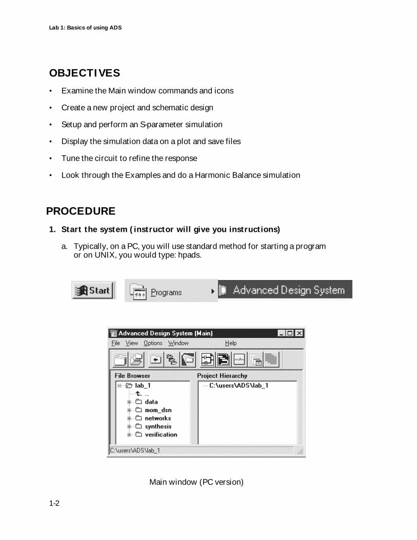
1. Start the system (instructor will give you instructions)
a. Typically, on a PC, you will use standard method for starting a programor on UNIX, you would type: hpads.
Main window (PC version)
Lab 1: Basics of using ADS
1-3
NOTE on Interface Differences between UNIX and PC:: The user interface forthe PC and UNIX are the same. The only difference is the appearance and some minorfeatures: For example, UNIX has tear-off menus; the PC version has a Toolbar thatcan be detached from the window. Otherwise, all the functions and commands are thesame for both platforms.
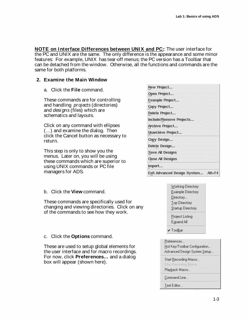
2. Examine the Main Window
a. Click the File command.
These commands are for controllingand handling projects (directories)and designs (files) which areschematics and layouts.
Click on any command with ellipses(…) and examine the dialog. Thenclick the Cancel button as necessary toreturn.
This step is only to show you themenus. Later on, you will be usingthese commands which are superior tousing UNIX commands or PC filemanagers for ADS.
b. Click the View command.
These commands are specifically used forchanging and viewing directories. Click on anyof the commands to see how they work.
c. Click the Options command.
These are used to setup global elements forthe user interface and for macro recordings.For now, click Preferences… and a dialogbox will appear (shown here).
Lab 1: Basics of using ADS
1-4
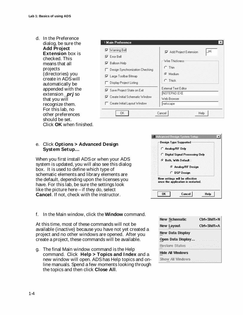
d. In the Preferencedialog, be sure theAdd ProjectExtension box ischecked. Thismeans that allprojects(directories) youcreate in ADS willautomatically beappended with theextension _prj sothat you willrecognize them.For this lab, noother preferencesshould be set.Click OK when finished.
e. Click Options > Advanced DesignSystem Setup…
When you first install ADS or when your ADSsystem is updated, you will also see this dialogbox. It is used to define which type ofschematic elements and library elements arethe default, depending upon the licenses youhave. For this lab, be sure the settings looklike the picture here – if they do, selectCancel. If not, check with the instructor.
f. In the Main window, click the Window command.
At this time, most of these commands will not beavailable (inactive) because you have not yet created aproject and no other windows are opened. After youcreate a project, these commands will be available.
g. The final Main window command is the Helpcommand. Click Help > Topics and Index and anew window will open. ADS has Help topics and on-line manuals. Spend a few moments looking throughthe topics and then click Close All.
Lab 1: Basics of using ADS
1-5
3. Create a new Project
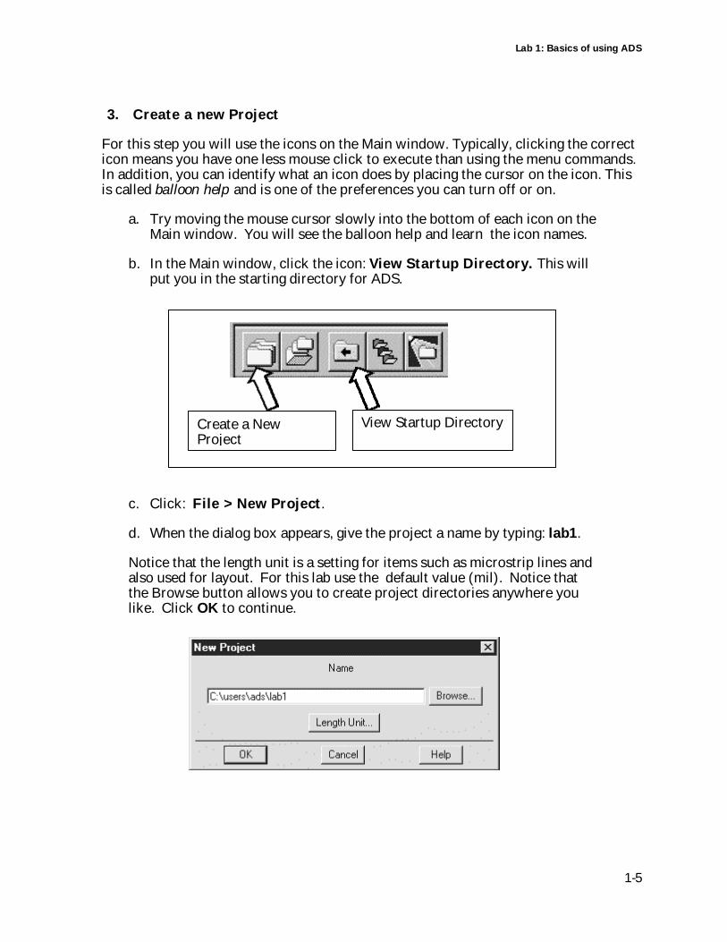
For this step you will use the icons on the Main window. Typically, clicking the correcticon means you have one less mouse click to execute than using the menu commands.In addition, you can identify what an icon does by placing the cursor on the icon. Thisis called balloon help and is one of the preferences you can turn off or on.
a. Try moving the mouse cursor slowly into the bottom of each icon on theMain window. You will see the balloon help and learn the icon names.
b. In the Main window, click the icon: View Startup Directory. This willput you in the starting directory for ADS.
c. Click: File > New Project.
d. When the dialog box appears, give the project a name by typing: lab1.
Notice that the length unit is a setting for items such as microstrip lines andalso used for layout. For this lab use the default value (mil). Notice thatthe Browse button allows you to create project directories anywhere youlike. Click OK to continue.
Create a NewProject
View Startup Directory
Lab 1: Basics of using ADS
1-6
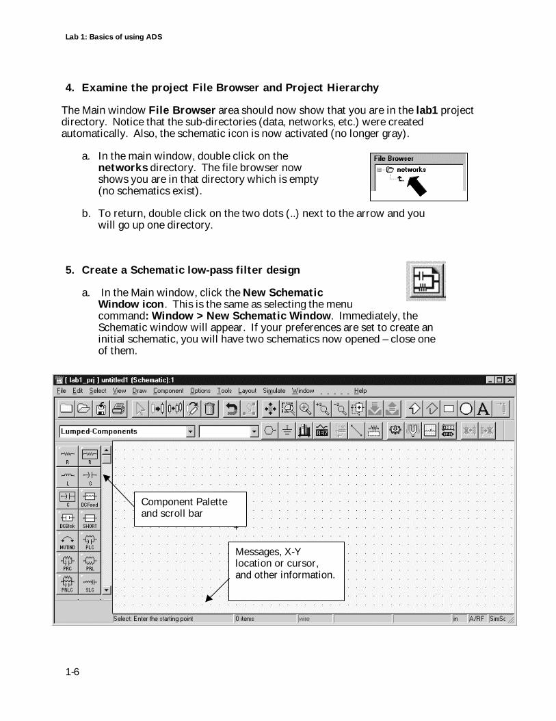
4. Examine the project File Browser and Project Hierarchy
The Main window File Browser area should now show that you are in the lab1 projectdirectory. Notice that the sub-directories (data, networks, etc.) were createdautomatically. Also, the schematic icon is now activated (no longer gray).
a. In the main window, double click on thenetworks directory. The file browser nowshows you are in that directory which is empty(no schematics exist).
b. To return, double click on the two dots (..) next to the arrow and youwill go up one directory.
5. Create a Schematic low-pass filter design
a. In the Main window, click the New SchematicWindow icon. This is the same as selecting the menucommand: Window > New Schematic Window. Immediately, theSchematic window will appear. If your preferences are set to create aninitial schematic, you will have two schematics now opened – close oneof them.
Component Paletteand scroll bar
Messages, X-Ylocation or cursor,and other information.
Lab 1: Basics of using ADS
1-7
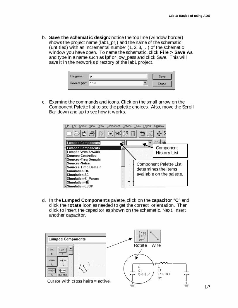
b. Save the schematic design: notice the top line (window border)shows the project name (lab1_prj) and the name of the schematic(untitled) with an incremental number (1, 2, 3, …) of the schematicwindow you have open. To name the schematic, click File > Save Asand type in a name such as lpf or low_pass and click Save. This willsave it in the networks directory of the lab1 project.
c. Examine the commands and icons. Click on the small arrow on theComponent Palette list to see the palette choices. Also, move the ScrollBar down and up to see how it works.
d. In the Lumped Components palette, click on the capacitor “C” andclick the rotate icon as needed to get the correct orientation. Thenclick to insert the capacitor as shown on the schematic. Next, insertanother capacitor.
Rotate Wire
Cursor with cross hairs = active.
ComponentHistory List
Component Palette Listdetermines the itemsavailable on the palette.
Lab 1: Basics of using ADS
1-8
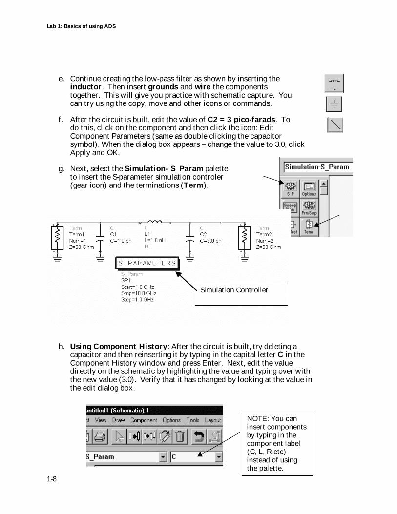
e. Continue creating the low-pass filter as shown by inserting theinductor. Then insert grounds and wire the componentstogether. This will give you practice with schematic capture. Youcan try using the copy, move and other icons or commands.
f. After the circuit is built, edit the value of C2 = 3 pico-farads. Todo this, click on the component and then click the icon: EditComponent Parameters (same as double clicking the capacitorsymbol). When the dialog box appears – change the value to 3.0, clickApply and OK.
g. Next, select the Simulation- S_Param paletteto insert the S-parameter simulation controler(gear icon) and the terminations (Term).
h. Using Component History: After the circuit is built, try deleting acapacitor and then reinserting it by typing in the capital letter C in theComponent History window and press Enter. Next, edit the valuedirectly on the schematic by highlighting the value and typing over withthe new value (3.0). Verify that it has changed by looking at the value inthe edit dialog box.
NOTE: You caninsert componentsby typing in thecomponent label(C, L, R etc)instead of usingthe palette.
Simulation Controller
Lab 1: Basics of using ADS
1-9
6. Setup and Run the Simulation
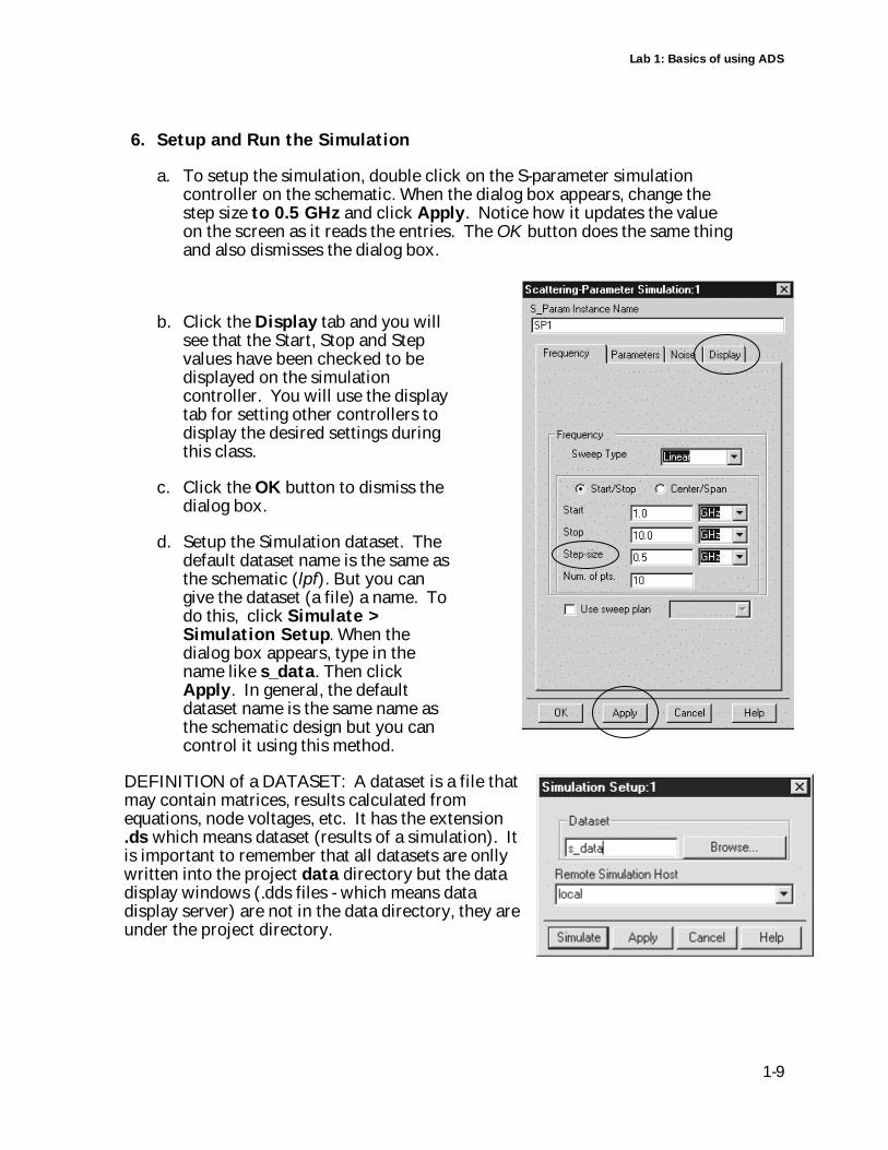
a. To setup the simulation, double click on the S-parameter simulationcontroller on the schematic. When the dialog box appears, change thestep size to 0.5 GHz and click Apply. Notice how it updates the valueon the screen as it reads the entries. The OK button does the same thingand also dismisses the dialog box.
b. Click the Display tab and you willsee that the Start, Stop and Stepvalues have been checked to bedisplayed on the simulationcontroller. You will use the displaytab for setting other controllers todisplay the desired settings duringthis class.
c. Click the OK button to dismiss thedialog box.
d. Setup the Simulation dataset. Thedefault dataset name is the same asthe schematic (lpf). But you cangive the dataset (a file) a name. Todo this, click Simulate >Simulation Setup. When thedialog box appears, type in thename like s_data. Then clickApply. In general, the defaultdataset name is the same name asthe schematic design but you cancontrol it using this method.
DEFINITION of a DATASET: A dataset is a file thatmay contain matrices, results calculated fromequations, node voltages, etc. It has the extension.ds which means dataset (results of a simulation). Itis important to remember that all datasets are onllywritten into the project data directory but the datadisplay windows (.dds files - which means datadisplay server) are not in the data directory, they areunder the project directory.
Lab 1: Basics of using ADS
1-10
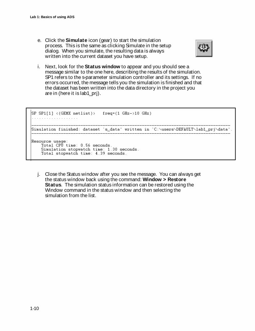
e. Click the Simulate icon (gear) to start the simulationprocess. This is the same as clicking Simulate in the setupdialog. When you simulate, the resulting data is alwayswritten into the current dataset you have setup.
i. Next, look for the Status window to appear and you should see amessage similar to the one here, describing the results of the simulation.SP1 refers to the s-parameter simulation controller and its settings. If noerrors occurred, the message tells you the simulation is finished and thatthe dataset has been written into the data directory in the project youare in (here it is lab1_prj).
j. Close the Status window after you see the message. You can always getthe status window back using the command: Window > RestoreStatus. The simulation status information can be restored using theWindow command in the status window and then selecting thesimulation from the list.
Lab 1: Basics of using ADS
1-11
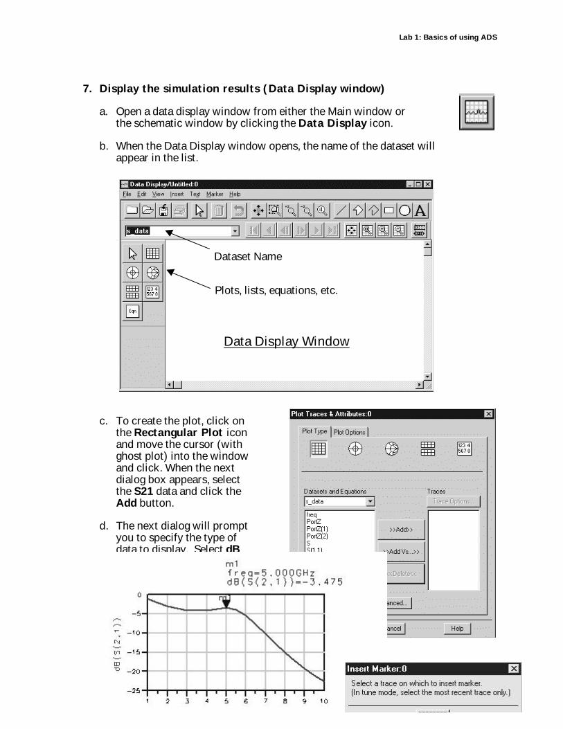
7. Display the simulation results (Data Display window)
a. Open a data display window from either the Main window orthe schematic window by clicking the Data Display icon.
b. When the Data Display window opens, the name of the dataset willappear in the list.
c. To create the plot, click onthe Rectangular Plot iconand move the cursor (withghost plot) into the windowand click. When the nextdialog box appears, selectthe S21 data and click theAdd button.
d. The next dialog will promptyou to specify the type ofdata to display. Select dBand click OK. The plotshould show a reasonablelow pass filter response.
e. Put a marker on the trace:Click the menu command:
Data Display Window
Dataset Name
Plots, lists, equations, etc.
Lab 1: Basics of using ADS
1-12
Marker > New. Select the trace and click to insert the marker. Movethe marker using the cursor or the keyboard arrow keys. Also, move themarker text by selecting it and positioning it as desired. Try deleting themarker or putting another marker on the trace.
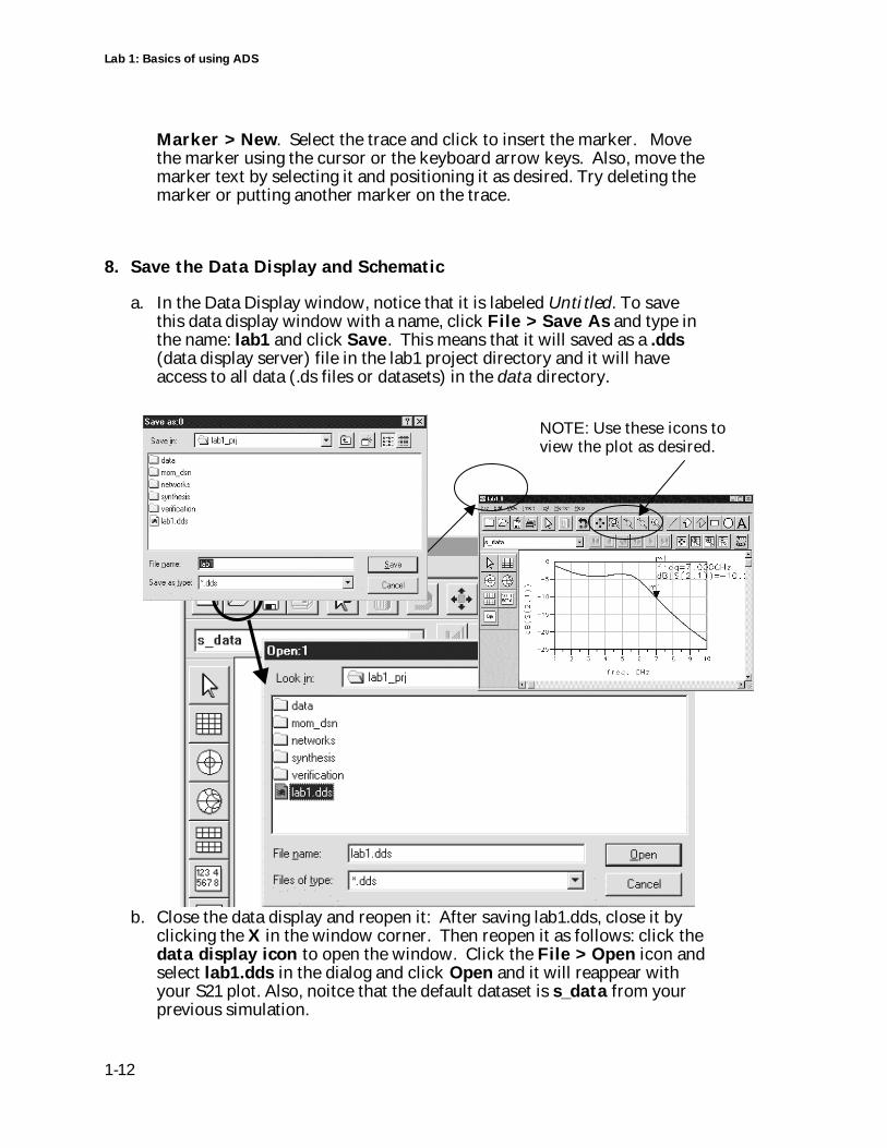
8. Save the Data Display and Schematic
a. In the Data Display window, notice that it is labeled Untitled. To savethis data display window with a name, click File > Save As and type inthe name: lab1 and click Save. This means that it will saved as a .dds(data display server) file in the lab1 project directory and it will haveaccess to all data (.ds files or datasets) in the data directory.
b. Close the data display and reopen it: After saving lab1.dds, close it byclicking the X in the window corner. Then reopen it as follows: click thedata display icon to open the window. Click the File > Open icon andselect lab1.dds in the dialog and click Open and it will reappear withyour S21 plot. Also, noitce that the default dataset is s_data from yourprevious simulation.
NOTE: Use these icons toview the plot as desired.

Lab 1: Basics of using ADS
1-13
9. Tune the filter circuit
This step introduces the ADS tuning feature that allows you to alter the parametervalue(s) of components and see the simulation results. In this step, you first select thecomponents and then select the tuning feature. If you select the tuning feature first,you must select the component parameters and not the components.
a. First, in the filter schematic, select (click) the capacitor and inductor tobe tuned as shown. Hold down the SHIFT or Ctrl key to select multiplecomponents: C1 and L1.
b. Position the data display and the schematic so that you can see themboth on the screen. If necessary, size the windows and use the View Allcommand or icon.
c. Click the command Simulate > Tuning or click the tuning icon.Immediately, the status (simulation) window will appear along with thetune control dialog box (shown here). Go ahead using the defaultsettings and tune the filter as you watch the data traces appear.
View All
TuningMove the slider or click on thebuttons to tune values. Noticehow the new traces appear onthe s_data plot after eachchange.
Each tuning creates anothertrace. The marker moves tothe most recent simulated(tuned) trace, which is red.This trace is the s_data datasetwhich is changed each timeyou tune (simulate).
Lab 1: Basics of using ADS
1-14
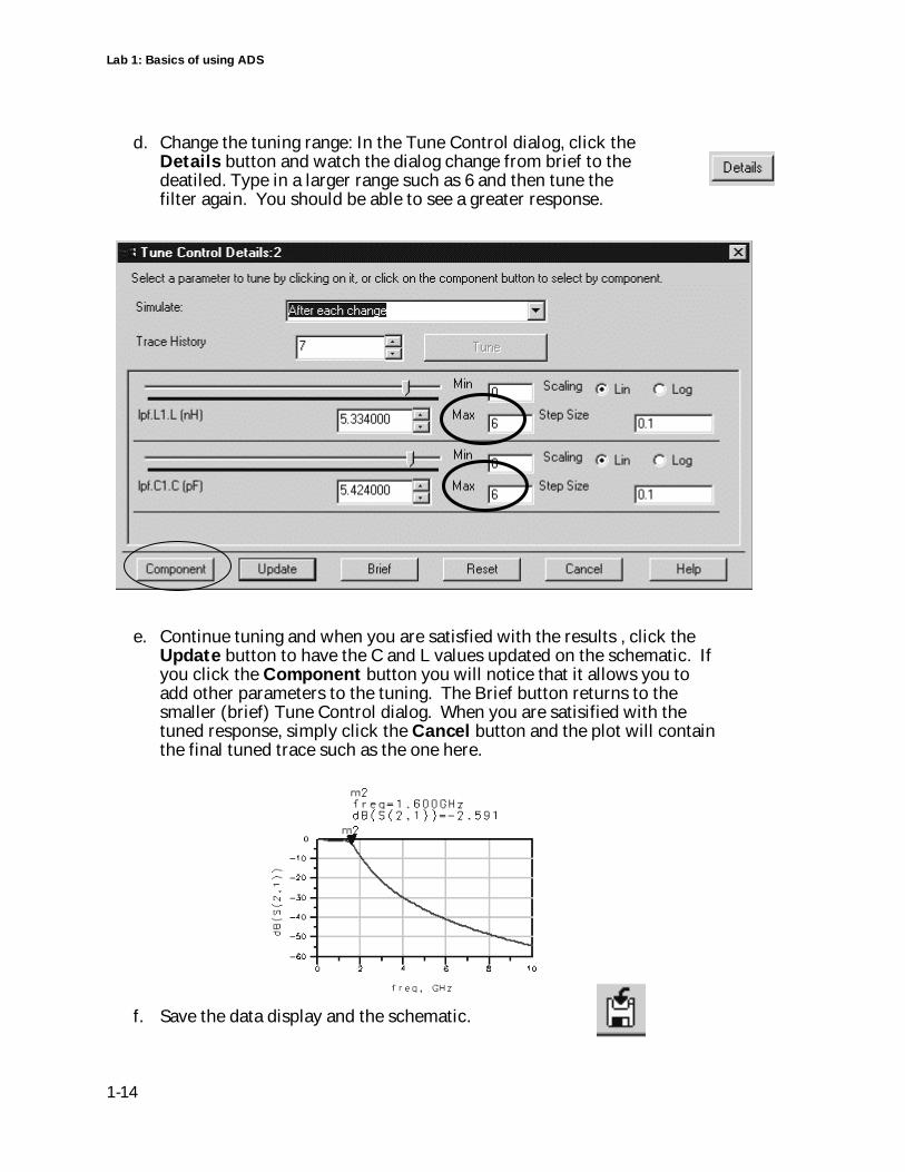
d. Change the tuning range: In the Tune Control dialog, click theDetails button and watch the dialog change from brief to thedeatiled. Type in a larger range such as 6 and then tune thefilter again. You should be able to see a greater response.
e. Continue tuning and when you are satisfied with the results , click theUpdate button to have the C and L values updated on the schematic. Ifyou click the Component button you will notice that it allows you toadd other parameters to the tuning. The Brief button returns to thesmaller (brief) Tune Control dialog. When you are satisified with thetuned response, simply click the Cancel button and the plot will containthe final tuned trace such as the one here.
f. Save the data display and the schematic.
Change theranges here.
Changesimulation
Lab 1: Basics of using ADS
1-15
10. Using Templates
Templates make it easy to include the required simulation controllers, ports,and other items used in the simulation. In addition, you can create your owntemplates or customize the existing ones.
a. From the Main window, click the Schematic icon and anotherschematic window will open.
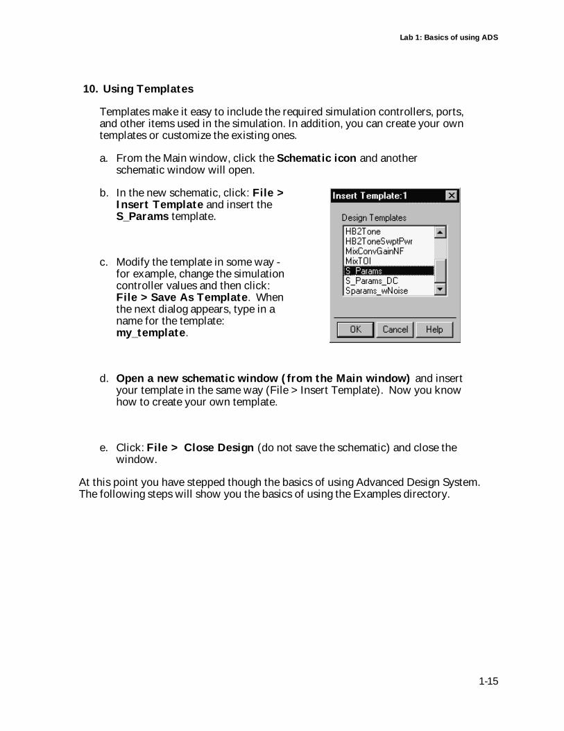
b. In the new schematic, click: File >Insert Template and insert theS_Params template.
c. Modify the template in some way -for example, change the simulationcontroller values and then click:File > Save As Template. Whenthe next dialog appears, type in aname for the template:my_template.
d. Open a new schematic window (from the Main window) and insertyour template in the same way (File > Insert Template). Now you knowhow to create your own template.
e. Click: File > Close Design (do not save the schematic) and close thewindow.
At this point you have stepped though the basics of using Advanced Design System.The following steps will show you the basics of using the Examples directory.
Lab 1: Basics of using ADS
1-16
About the Examples Directory
All of the examples can be examined, including the results of the simulations.However, because the example files should remain unchanged, copy them intoyour own directory to simulate or modify them.
11. Open the Example Directory: RFIC, amplifier_prj, HBtest.dsn
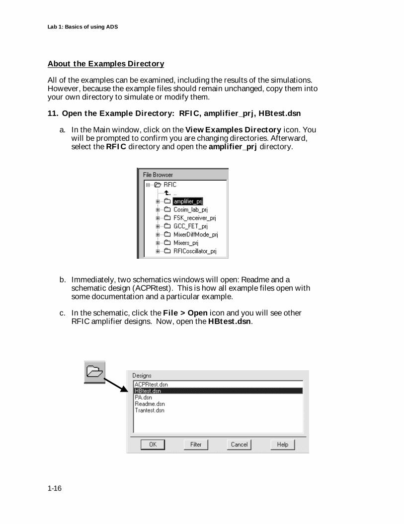
a. In the Main window, click on the View Examples Directory icon. Youwill be prompted to confirm you are changing directories. Afterward,select the RFIC directory and open the amplifier_prj directory.
b. Immediately, two schematics windows will open: Readme and aschematic design (ACPRtest). This is how all example files open withsome documentation and a particular example.
c. In the schematic, click the File > Open icon and you will see otherRFIC amplifier designs. Now, open the HBtest.dsn.
Lab 1: Basics of using ADS
1-17
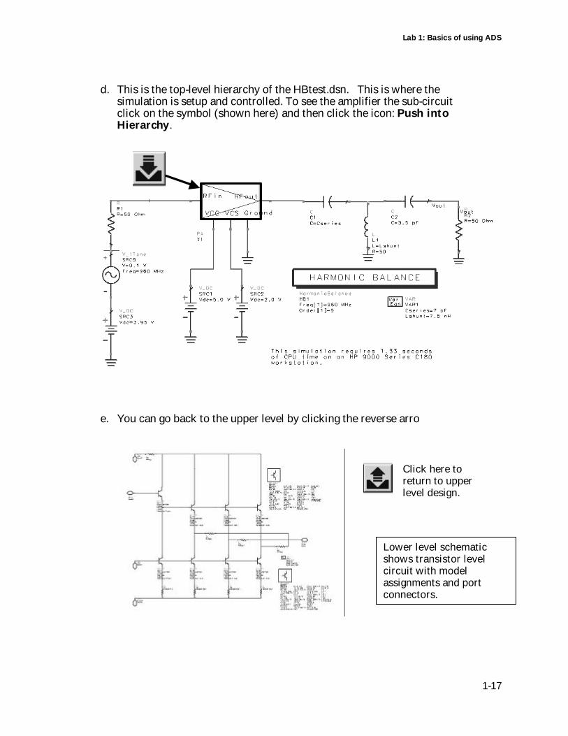
d. This is the top-level hierarchy of the HBtest.dsn. This is where thesimulation is setup and controlled. To see the amplifier the sub-circuitclick on the symbol (shown here) and then click the icon: Push intoHierarchy.
e. You can go back to the upper level by clicking the reverse arro
Lower level schematicshows transistor levelcircuit with modelassignments and portconnectors.
Click here toreturn to upperlevel design.
Lab 1: Basics of using ADS
1-18
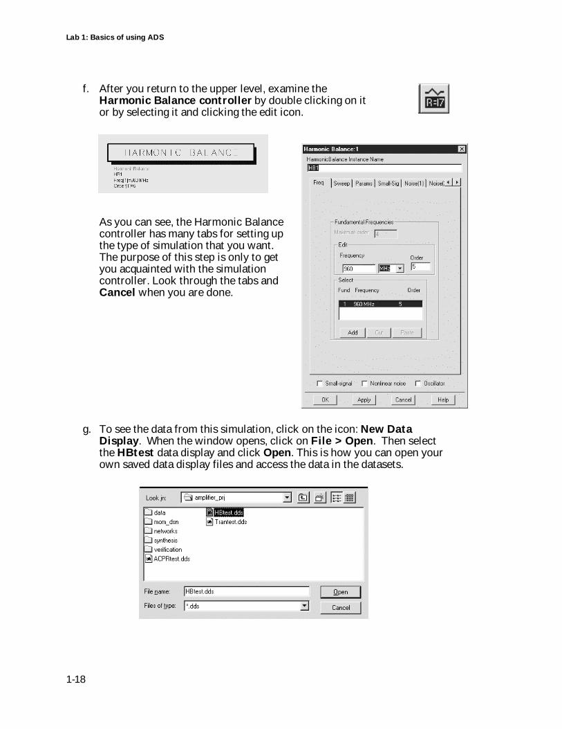
f. After you return to the upper level, examine theHarmonic Balance controller by double clicking on itor by selecting it and clicking the edit icon.
As you can see, the Harmonic Balancecontroller has many tabs for setting upthe type of simulation that you want.The purpose of this step is only to getyou acquainted with the simulationcontroller. Look through the tabs andCancel when you are done.
g. To see the data from this simulation, click on the icon: New DataDisplay. When the window opens, click on File > Open. Then selectthe HBtest data display and click Open. This is how you can open yourown saved data display files and access the data in the datasets.
Lab 1: Basics of using ADS
1-19
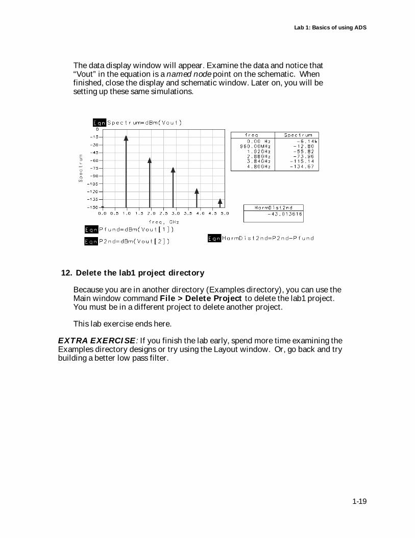
The data display window will appear. Examine the data and notice that“Vout” in the equation is a named node point on the schematic. Whenfinished, close the display and schematic window. Later on, you will besetting up these same simulations.
12. Delete the lab1 project directory
Because you are in another directory (Examples directory), you can use theMain window command File > Delete Project to delete the lab1 project.You must be in a different project to delete another project.
This lab exercise ends here.
EXTRA EXERCISE: If you finish the lab early, spend more time examining theExamples directory designs or try using the Layout window. Or, go back and trybuilding a better low pass filter.

2
.
This chapter introduces the mixer circuit and shows all the basicsof DC simulations, including a family of curves and device biasingcalculations.
Lab 2: DC Simulations
Lab 2: DC Simulations
2-2
OBJECTIVES
• Build a symbolized sub-circuit for use in the hierarchy
• Create a family of curves for the device used in the mixer
• Sweep variables, pass parameters, and the plot or list the data
• Use equations to calculate bias resistor values from simulation data
NOTE about this lab: This lab and the remaining labs will use the BJT mixer todemonstrate all types of simulations. Regardless of the type of circuit you design, thetechniques and simulations presented in these labs will be applicable to many othercircuit configurations.
PROCEDURE
The following steps are for creating the mixer BJT sub-circuit with package parasiticsand performing the dc simulations as part of the design process.
1. Create a New Project and name it: mixer
2. Open a New Schematic Window and save it as: bjt_pkg
3. Setup the BJT device and model:
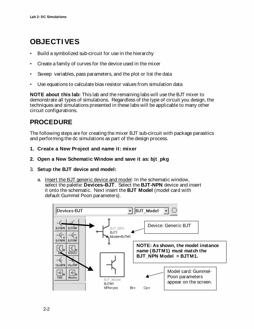
a. Insert the BJT generic device and model: In the schematic window,select the palette: Devices–BJT. Select the BJT-NPN device and insertit onto the schematic. Next insert the BJT Model (model card withdefault Gummel Poon parameters).
Device: Generic BJT
Model card: Gummel-Poon parametersappear on the screen.
NOTE: As shown, the model instancename (BJTM1) must match theBJT_NPN Model = BJTM1.
Lab 2: DC Simulations
2-3
b. Double click on the model. When the dialog appears, click ComponentOptions and in the next dialog, click Clear All and OK. This willremove the parameter list from the schematic.
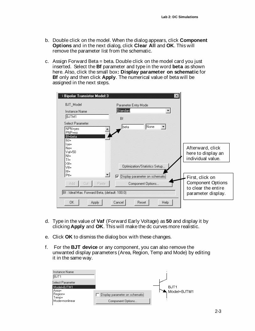
c. Assign Forward Beta = beta. Double click on the model card you justinserted. Select the Bf parameter and type in the word beta as shownhere. Also, click the small box: Display parameter on schematic forBf only and then click Apply. The numerical value of beta will beassigned in the next steps.
d. Type in the value of Vaf (Forward Early Voltage) as 50 and display it byclicking Apply and OK. This will make the dc curves more realistic.
e. Click OK to dismiss the dialog box with these changes.
f. For the BJT device or any component, you can also remove theunwanted display parameters (Area, Region, Temp and Mode) by editingit in the same way.
First, click onComponent Optionsto clear the entireparameter display.
Afterward, clickhere to display anindividual value.
Lab 2: DC Simulations
2-4
4. Build the rest of the subcircuit
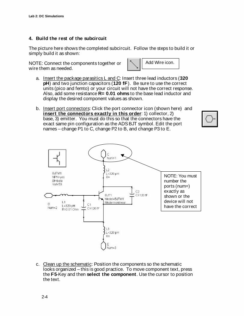
The picture here shows the completed subcircuit. Follow the steps to build it orsimply build it as shown:
NOTE: Connect the components together orwire them as needed.
a. Insert the package parasitics L and C: Insert three lead inductors (320pH) and two junction capacitors (120 fF). Be sure to use the correctunits (pico and femto) or your circuit will not have the correct response.Also, add some resistance R= 0.01 ohms to the base lead inductor anddisplay the desired component values as shown.
b. Insert port connectors: Click the port connector icon (shown here) andinsert the connectors exactly in this order: 1) collector, 2)base, 3) emitter. You must do this so that the connectors have theexact same pin configuration as the ADS BJT symbol. Edit the portnames – change P1 to C, change P2 to B, and change P3 to E.
c. Clean up the schematic: Position the components so the schematiclooks organized – this is good practice. To move component text, pressthe F5-Key and then select the component. Use the cursor to positionthe text.
Add Wire icon.
NOTE: You mustnumber theports (num=)exactly asshown or thedevice will nothave the correctorientation.
Lab 2: DC Simulations
2-5
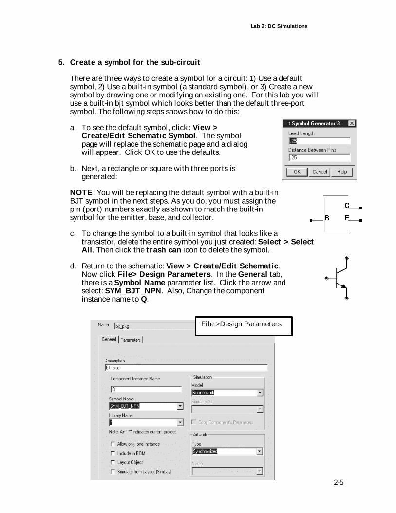
5. Create a symbol for the sub-circuit
There are three ways to create a symbol for a circuit: 1) Use a defaultsymbol, 2) Use a built-in symbol (a standard symbol), or 3) Create a newsymbol by drawing one or modifying an existing one. For this lab you willuse a built-in bjt symbol which looks better than the default three-portsymbol. The following steps shows how to do this:
a. To see the default symbol, click: View >Create/Edit Schematic Symbol. The symbolpage will replace the schematic page and a dialogwill appear. Click OK to use the defaults.
b. Next, a rectangle or square with three ports isgenerated:
NOTE: You will be replacing the default symbol with a built-inBJT symbol in the next steps. As you do, you must assign thepin (port) numbers exactly as shown to match the built-insymbol for the emitter, base, and collector.
c. To change the symbol to a built-in symbol that looks like atransistor, delete the entire symbol you just created: Select > SelectAll. Then click the trash can icon to delete the symbol.
d. Return to the schematic: View > Create/Edit Schematic.Now click File> Design Parameters. In the General tab,there is a Symbol Name parameter list. Click the arrow andselect: SYM_BJT_NPN. Also, Change the componentinstance name to Q.
File >Design Parameters
Lab 2: DC Simulations
2-6
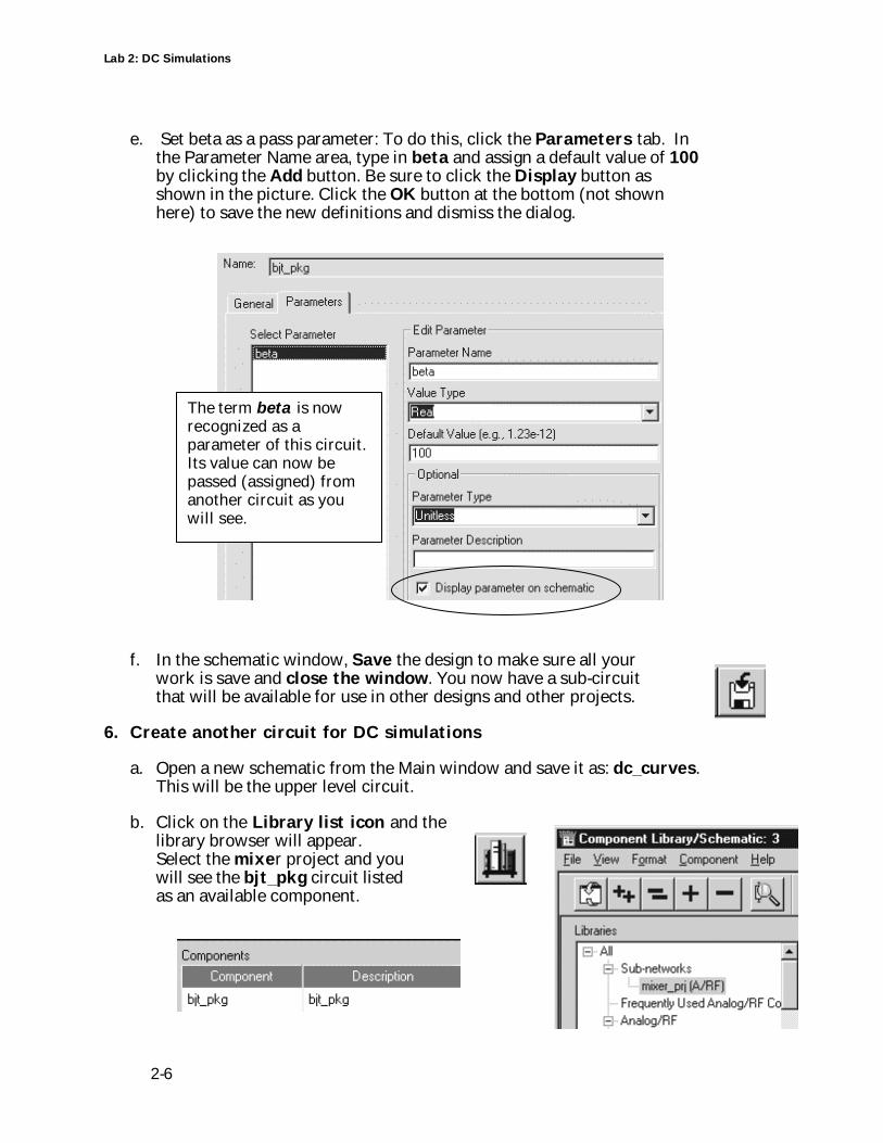
e. Set beta as a pass parameter: To do this, click the Parameters tab. Inthe Parameter Name area, type in beta and assign a default value of 100by clicking the Add button. Be sure to click the Display button asshown in the picture. Click the OK button at the bottom (not shownhere) to save the new definitions and dismiss the dialog.
f. In the schematic window, Save the design to make sure all yourwork is save and close the window. You now have a sub-circuitthat will be available for use in other designs and other projects.
6. Create another circuit for DC simulations
a. Open a new schematic from the Main window and save it as: dc_curves.This will be the upper level circuit.
b. Click on the Library list icon and thelibrary browser will appear.Select the mixer project and youwill see the bjt_pkg circuit listedas an available component.
The term beta is nowrecognized as aparameter of this circuit.Its value can now bepassed (assigned) fromanother circuit as youwill see.
Lab 2: DC Simulations
2-7
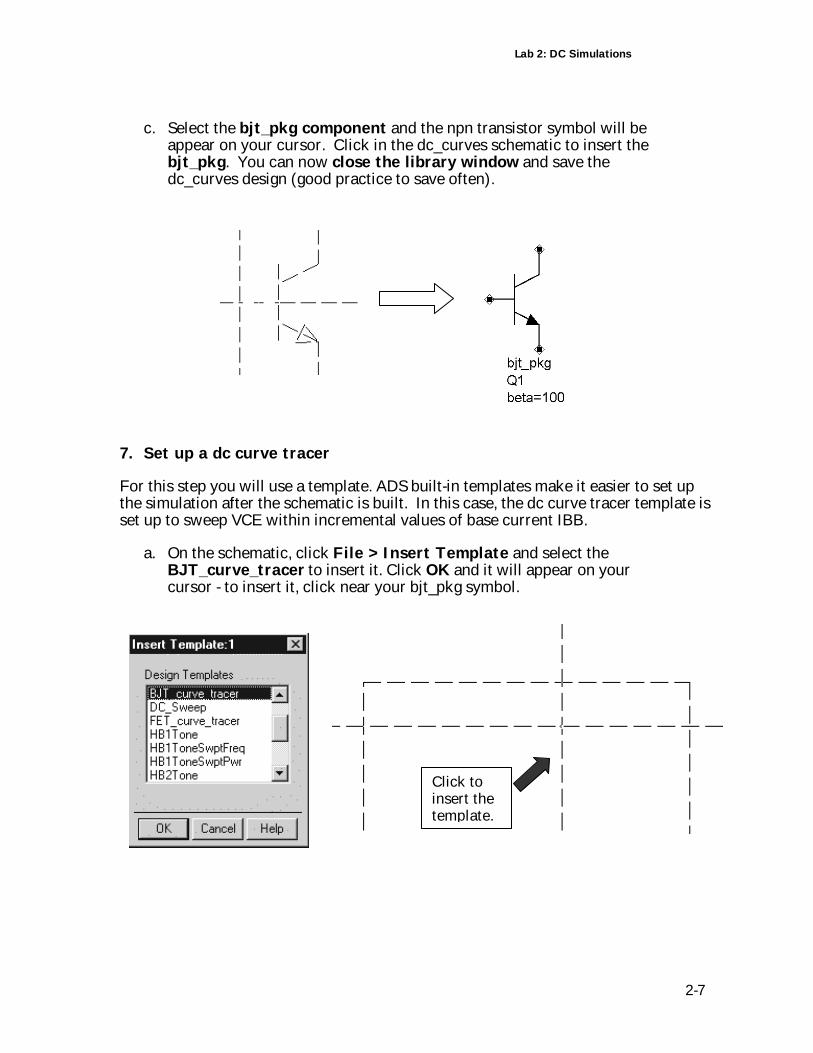
c. Select the bjt_pkg component and the npn transistor symbol will beappear on your cursor. Click in the dc_curves schematic to insert thebjt_pkg. You can now close the library window and save thedc_curves design (good practice to save often).
7. Set up a dc curve tracer
For this step you will use a template. ADS built-in templates make it easier to set upthe simulation after the schematic is built. In this case, the dc curve tracer template isset up to sweep VCE within incremental values of base current IBB.
a. On the schematic, click File > Insert Template and select theBJT_curve_tracer to insert it. Click OK and it will appear on yourcursor - to insert it, click near your bjt_pkg symbol.
Click toinsert thetemplate.
Lab 2: DC Simulations
2-8
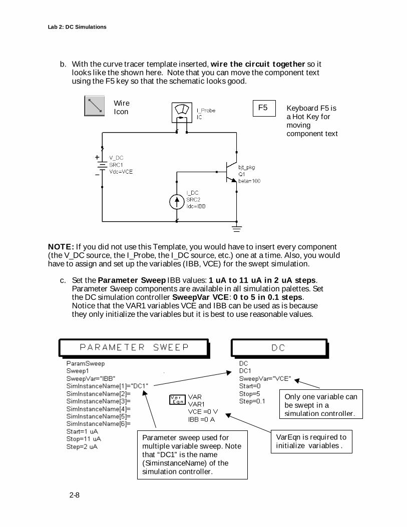
b. With the curve tracer template inserted, wire the circuit together so itlooks like the shown here. Note that you can move the component textusing the F5 key so that the schematic looks good.
NOTE: If you did not use this Template, you would have to insert every component(the V_DC source, the I_Probe, the I_DC source, etc.) one at a time. Also, you wouldhave to assign and set up the variables (IBB, VCE) for the swept simulation.
c. Set the Parameter Sweep IBB values: 1 uA to 11 uA in 2 uA steps.Parameter Sweep components are available in all simulation palettes. Setthe DC simulation controller SweepVar VCE: 0 to 5 in 0.1 steps.Notice that the VAR1 variables VCE and IBB can be used as is becausethey only initialize the variables but it is best to use reasonable values.
Parameter sweep used formultiple variable sweep. Notethat “DC1” is the name(SiminstanceName) of thesimulation controller.
VarEqn is required toinitialize variables .
Only one variable canbe swept in asimulation controller.
F5WireIcon Keyboard F5 is
a Hot Key formovingcomponent text
Lab 2: DC Simulations
2-9
8. Name the dataset and run the simulation
a. Click Simulate > SimulationSetup. When the dialog appears,type in a name for the datasetdc_curves as shown.
b. Click Apply and Simulate.
c. After the simulation is finished, clickthe Cancel button and the setupdialog will disappear. If you get anerror message, check the simulationset up and repeat if necessary.
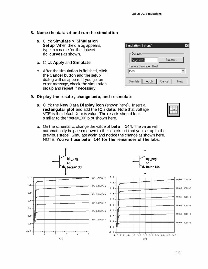
9. Display the results, change beta, and resimulate
a. Click the New Data Display icon (shown here). Insert arectangular plot and add the IC.i data. Note that voltageVCE is the default X-axis value. The results should looksimilar to the “beta=100” plot shown here.
b. On the schematic, change the value of beta = 144. The value willautomatically be passed down to the sub circuit that you set up in theprevious steps. Simulate again and notice the change as shown here.NOTE: You will use beta =144 for the remainder of the labs.
Lab 2: DC Simulations
2-10
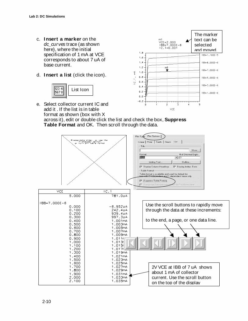
c. Insert a marker on thedc_curves trace (as shownhere), where the initialspecification of 1 mA at VCEcorresponds to about 7 uA ofbase current.
d. Insert a list (click the icon).
e. Select collector current IC andadd it . If the list is in tableformat as shown (box with Xacross it), edit or double click the list and check the box, SuppressTable Format and OK. Then scroll through the data.
The markertext can beselectedand moved.
2V VCE at IBB of 7 uA showsabout 1 mA of collectorcurrent. Use the scroll buttonon the top of the display
Use the scroll buttons to rapidly movethrough the data at these increments:
to the end, a page, or one data line.
List Icon
Lab 2: DC Simulations
2-11
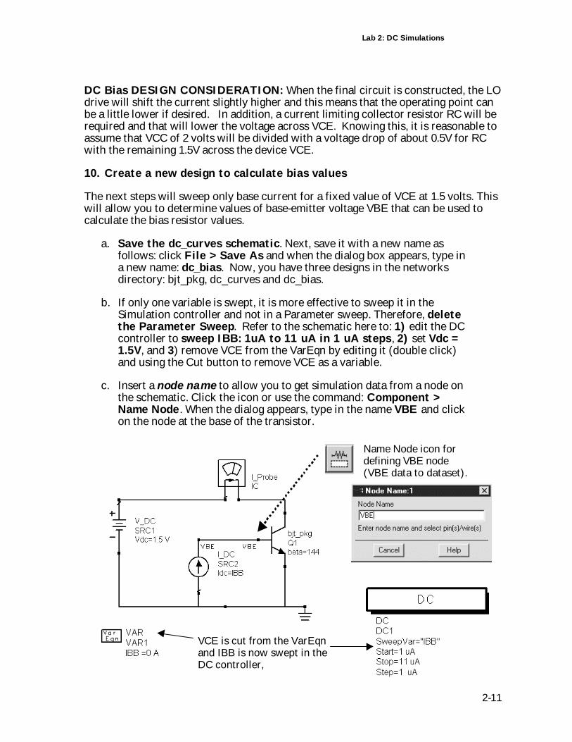
DC Bias DESIGN CONSIDERATION: When the final circuit is constructed, the LOdrive will shift the current slightly higher and this means that the operating point canbe a little lower if desired. In addition, a current limiting collector resistor RC will berequired and that will lower the voltage across VCE. Knowing this, it is reasonable toassume that VCC of 2 volts will be divided with a voltage drop of about 0.5V for RCwith the remaining 1.5V across the device VCE.
10. Create a new design to calculate bias values
The next steps will sweep only base current for a fixed value of VCE at 1.5 volts. Thiswill allow you to determine values of base-emitter voltage VBE that can be used tocalculate the bias resistor values.
a. Save the dc_curves schematic. Next, save it with a new name asfollows: click File > Save As and when the dialog box appears, type ina new name: dc_bias. Now, you have three designs in the networksdirectory: bjt_pkg, dc_curves and dc_bias.
b. If only one variable is swept, it is more effective to sweep it in theSimulation controller and not in a Parameter sweep. Therefore, deletethe Parameter Sweep. Refer to the schematic here to: 1) edit the DCcontroller to sweep IBB: 1uA to 11 uA in 1 uA steps, 2) set Vdc =1.5V, and 3) remove VCE from the VarEqn by editing it (double click)and using the Cut button to remove VCE as a variable.
c. Insert a node name to allow you to get simulation data from a node onthe schematic. Click the icon or use the command: Component >Name Node. When the dialog appears, type in the name VBE and clickon the node at the base of the transistor.
Name Node icon fordefining VBE node(VBE data to dataset).
VCE is cut from the VarEqnand IBB is now swept in theDC controller,
Lab 2: DC Simulations
2-12
d. Save and Simulate: Save the new design by clicking the save icon –this is always good practice. Next, check the dataset name: Simulation> Setup) as in the previous simulation. Be sure it appears as: dc_biasand then Simulate.
11. Display the data (dc_bias) in a list
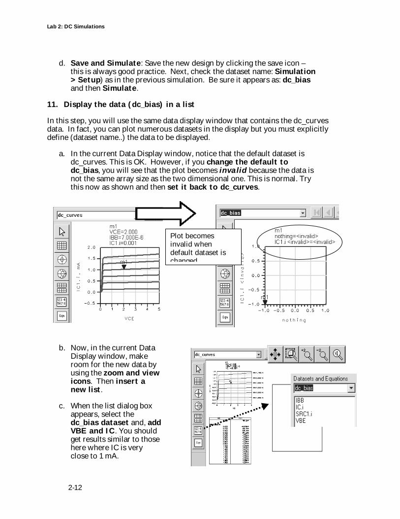
In this step, you will use the same data display window that contains the dc_curvesdata. In fact, you can plot numerous datasets in the display but you must explicitlydefine (dataset name..) the data to be displayed.
a. In the current Data Display window, notice that the default dataset isdc_curves. This is OK. However, if you change the default todc_bias, you will see that the plot becomes invalid because the data isnot the same array size as the two dimensional one. This is normal. Trythis now as shown and then set it back to dc_curves.
b. Now, in the current DataDisplay window, makeroom for the new data byusing the zoom and viewicons. Then insert anew list.
c. When the list dialog boxappears, select thedc_bias dataset and, addVBE and IC. You shouldget results similar to thosehere where IC is veryclose to 1 mA.
Plot becomesinvalid whendefault dataset ischanged.
Lab 2: DC Simulations
2-13
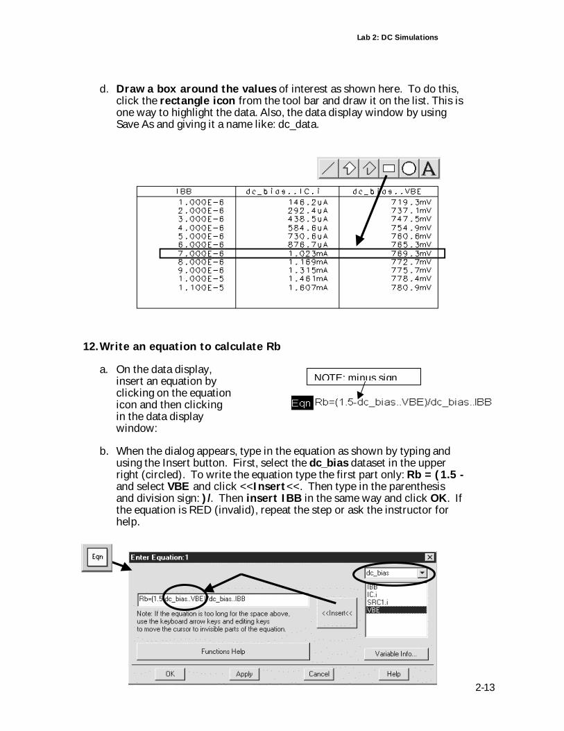
d. Draw a box around the values of interest as shown here. To do this,click the rectangle icon from the tool bar and draw it on the list. This isone way to highlight the data. Also, the data display window by usingSave As and giving it a name like: dc_data.
12. Write an equation to calculate Rb
a. On the data display,insert an equation byclicking on the equationicon and then clickingin the data displaywindow:
b. When the dialog appears, type in the equation as shown by typing andusing the Insert button. First, select the dc_bias dataset in the upperright (circled). To write the equation type the first part only: Rb = (1.5 -and select VBE and click <<Insert<<. Then type in the parenthesisand division sign: )/. Then insert IBB in the same way and click OK. Ifthe equation is RED (invalid), repeat the step or ask the instructor forhelp.
NOTE: minus sign
Lab 2: DC Simulations
2-14
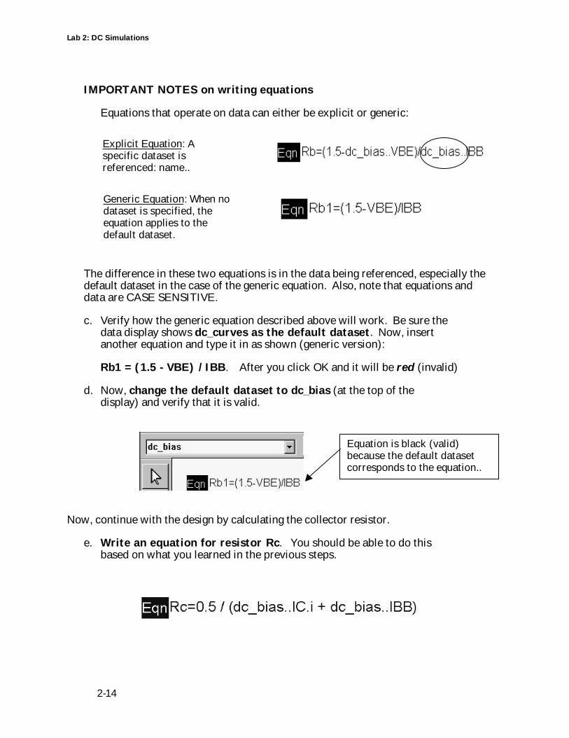
IMPORTANT NOTES on writing equations
Equations that operate on data can either be explicit or generic:
The difference in these two equations is in the data being referenced, especially thedefault dataset in the case of the generic equation. Also, note that equations anddata are CASE SENSITIVE.
c. Verify how the generic equation described above will work. Be sure thedata display shows dc_curves as the default dataset. Now, insertanother equation and type it in as shown (generic version):
Rb1 = (1.5 - VBE) / IBB. After you click OK and it will be red (invalid)
d. Now, change the default dataset to dc_bias (at the top of thedisplay) and verify that it is valid.
Now, continue with the design by calculating the collector resistor.
e. Write an equation for resistor Rc. You should be able to do thisbased on what you learned in the previous steps.
Generic Equation: When nodataset is specified, theequation applies to thedefault dataset.
Explicit Equation: Aspecific dataset isreferenced: name..
Equation is black (valid)because the default datasetcorresponds to the equation..
Lab 2: DC Simulations
2-15
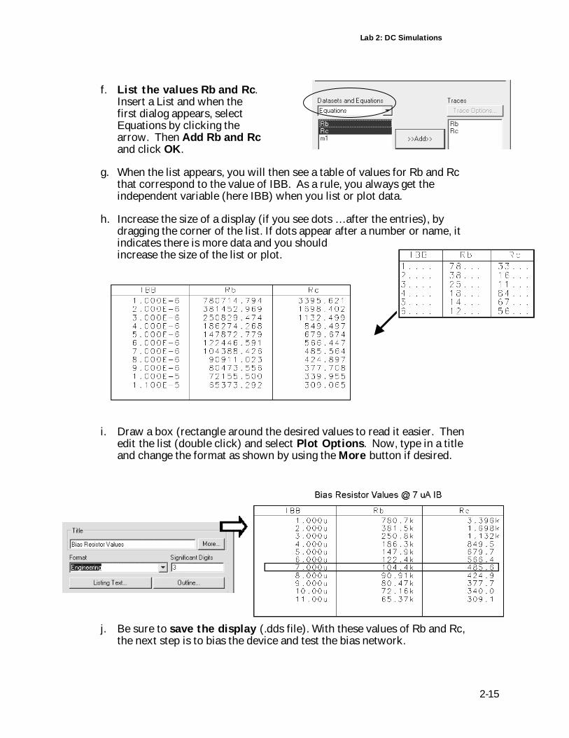
f. List the values Rb and Rc.Insert a List and when thefirst dialog appears, selectEquations by clicking thearrow. Then Add Rb and Rcand click OK.
g. When the list appears, you will then see a table of values for Rb and Rcthat correspond to the value of IBB. As a rule, you always get theindependent variable (here IBB) when you list or plot data.
h. Increase the size of a display (if you see dots …after the entries), bydragging the corner of the list. If dots appear after a number or name, itindicates there is more data and you shouldincrease the size of the list or plot.
i. Draw a box (rectangle around the desired values to read it easier. Thenedit the list (double click) and select Plot Options. Now, type in a titleand change the format as shown by using the More button if desired.
j. Be sure to save the display (.dds file). With these values of Rb and Rc,the next step is to bias the device and test the bias network.
Lab 2: DC Simulations
2-16
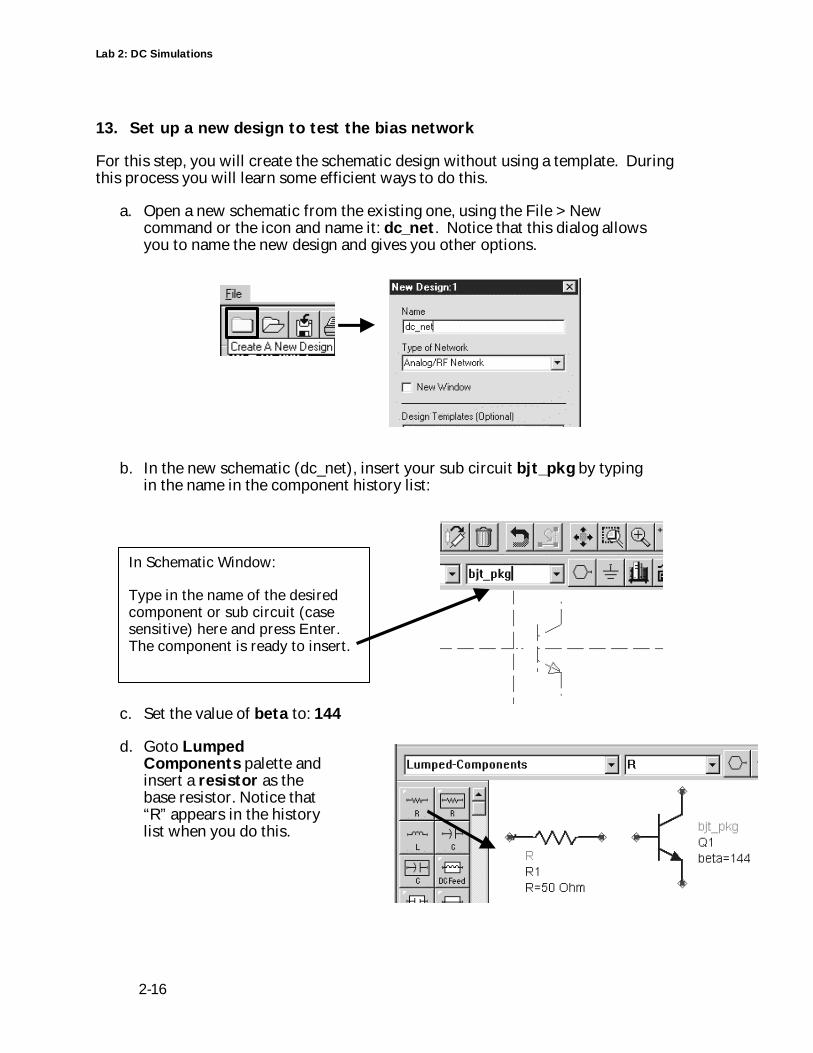
13. Set up a new design to test the bias network
For this step, you will create the schematic design without using a template. Duringthis process you will learn some efficient ways to do this.
a. Open a new schematic from the existing one, using the File > Newcommand or the icon and name it: dc_net. Notice that this dialog allowsyou to name the new design and gives you other options.
b. In the new schematic (dc_net), insert your sub circuit bjt_pkg by typingin the name in the component history list:
c. Set the value of beta to: 144
d. Goto LumpedComponents palette andinsert a resistor as thebase resistor. Notice that“R” appears in the historylist when you do this.
In Schematic Window:
Type in the name of the desiredcomponent or sub circuit (casesensitive) here and press Enter.The component is ready to insert.
Lab 2: DC Simulations
2-17
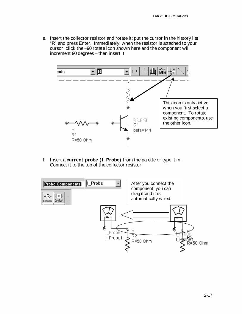
e. Insert the collector resistor and rotate it: put the cursor in the history list“R” and press Enter. Immediately, when the resistor is attached to yourcursor, click the –90 rotate icon shown here and the component willincrement 90 degrees – then insert it.
f. Insert a current probe (I_Probe) from the palette or type it in.Connect it to the top of the collector resistor.
After you connect thecomponent, you candrag it and it isautomatically wired.
This icon is only activewhen you first select acomponent. To rotateexisting components, usethe other icon.
Lab 2: DC Simulations
2-18
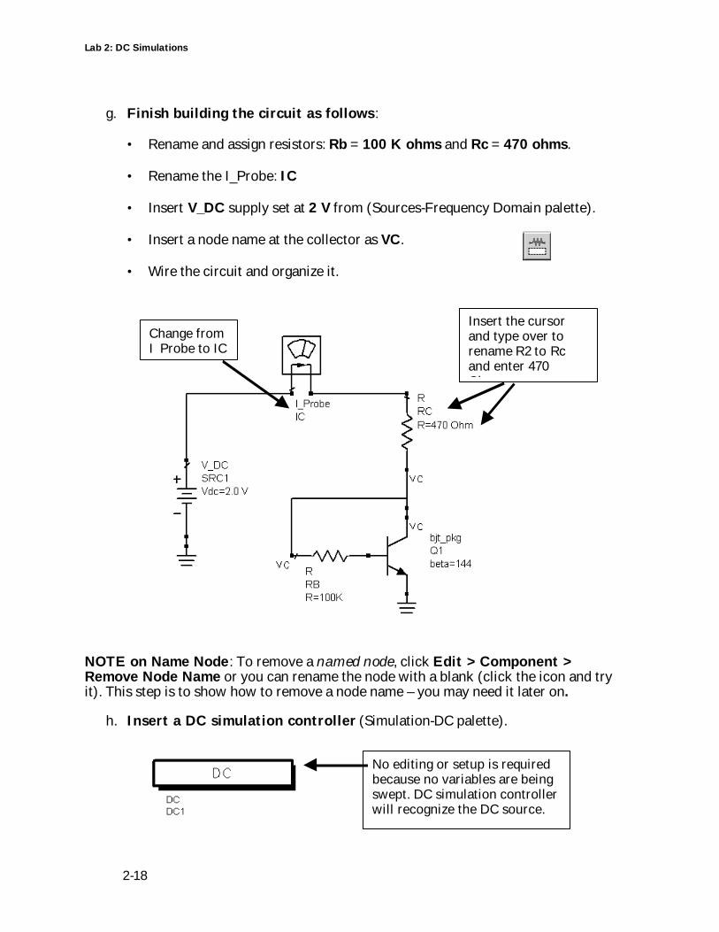
g. Finish building the circuit as follows:
• Rename and assign resistors: Rb = 100 K ohms and Rc = 470 ohms.
• Rename the I_Probe: IC
• Insert V_DC supply set at 2 V from (Sources-Frequency Domain palette).
• Insert a node name at the collector as VC.
• Wire the circuit and organize it.
NOTE on Name Node: To remove a named node, click Edit > Component >Remove Node Name or you can rename the node with a blank (click the icon and tryit). This step is to show how to remove a node name – you may need it later on.
h. Insert a DC simulation controller (Simulation-DC palette).
No editing or setup is requiredbecause no variables are beingswept. DC simulation controllerwill recognize the DC source.
Change fromI_Probe to IC
Insert the cursorand type over torename R2 to Rcand enter 470Ohms.
Lab 2: DC Simulations
2-19
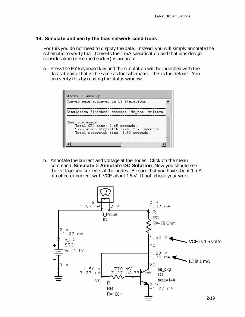
14. Simulate and verify the bias network conditions
For this you do not need to display the data. Instead, you will simply annotate theschematic to verify that IC meets the 1 mA specification and that bias designconsideration (described earlier) is accurate.
a. Press the F7 keyboard key and the simulation will be launched with thedataset name that is the same as the schematic – this is the default. Youcan verify this by reading the status window:
b. Annotate the current and voltage at the nodes. Click on the menucommand: Simulate > Annotate DC Solution. Now you should seethe voltage and currents at the nodes. Be sure that you have about 1 mAof collector current with VCE about 1.5 V. If not, check your work.
VCE is 1.5 volts
IC is 1 mA
Lab 2: DC Simulations
2-20
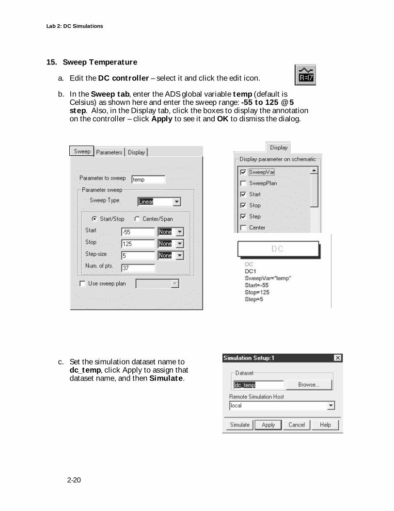
15. Sweep Temperature
a. Edit the DC controller – select it and click the edit icon.
b. In the Sweep tab, enter the ADS global variable temp (default isCelsius) as shown here and enter the sweep range: -55 to 125 @ 5step. Also, in the Display tab, click the boxes to display the annotationon the controller – click Apply to see it and OK to dismiss the dialog.
c. Set the simulation dataset name todc_temp, click Apply to assign thatdataset name, and then Simulate.
Lab 2: DC Simulations
2-21
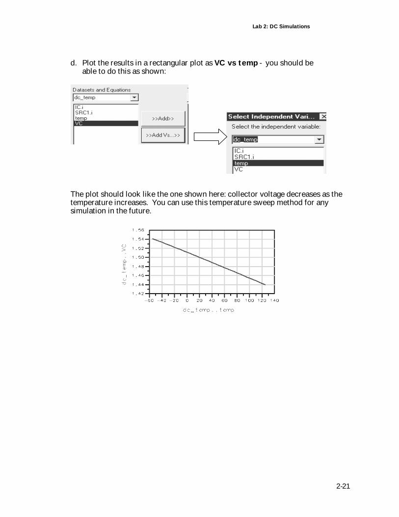
d. Plot the results in a rectangular plot as VC vs temp - you should beable to do this as shown:
The plot should look like the one shown here: collector voltage decreases as thetemperature increases. You can use this temperature sweep method for anysimulation in the future.
Lab 2: DC Simulations
2-22
EXTRA EXERCISES
1. Plot current (probe) vs. temperature.
2. Try these commands:
a. Select the bjt and click the command: Edit > Component > BreakConnections. Reinsert the bjt and see what happens.
b. Spend a few moments experimenting with the other Simulation menucommands: Highlight Node and Detailed Device Operating Point. Theseare only available after a dc simulation.
c. Go to the data display: Use the right mouse button and experimentwith the selections.
2. Replace the Gummel-Poon model card with another model (Mextram) andresimulate. Afterward, compare the results.
3
This chapter shows the basics of AC simulations, including smallsignal gain and noise. It also shows many detailed features of thesystem.
Lab 3: AC Simulations
Lab 3: AC Simulations
3-2
OBJECTIVES
• Perform AC small-signal and noise simulations
• Sweep variables, tune parameters, write equations
• Control plots, traces, datasets, and AC sources
About this lab: This lab continues the mixer project and uses the same sub-circuit asthe previous lab.
PROCEDURE
1. Use copy/paste to create a design
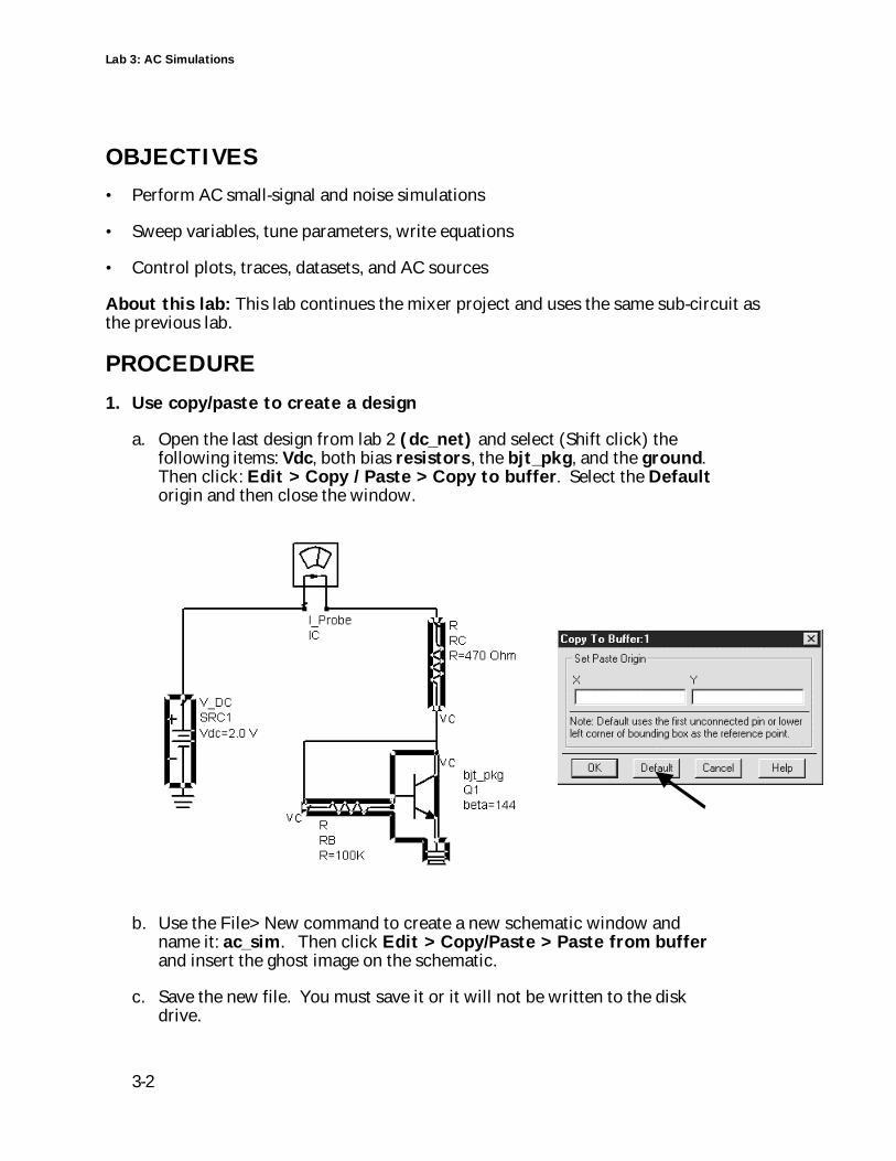
a. Open the last design from lab 2 (dc_net) and select (Shift click) thefollowing items: Vdc, both bias resistors, the bjt_pkg, and the ground.Then click: Edit > Copy / Paste > Copy to buffer. Select the Defaultorigin and then close the window.
b. Use the File> New command to create a new schematic window andname it: ac_sim. Then click Edit > Copy/Paste > Paste from bufferand insert the ghost image on the schematic.
c. Save the new file. You must save it or it will not be written to the diskdrive.
Lab 3: AC Simulations
3-3
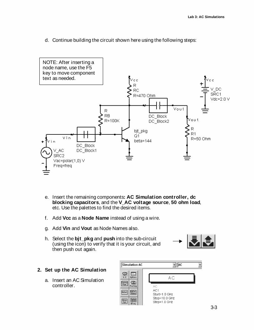
d. Continue building the circuit shown here using the following steps:
e. Insert the remaining components: AC Simulation controller, dcblocking capacitors, and the V_AC voltage source, 50 ohm load,etc. Use the palettes to find the desired items.
f. Add Vcc as a Node Name instead of using a wire.
g. Add Vin and Vout as Node Names also.
h. Select the bjt_pkg and push into the sub-circuit(using the icon) to verify that it is your circuit, andthen push out again.
2. Set up the AC Simulation
a. Insert an AC Simulationcontroller.
NOTE: After inserting anode name, use the F5key to move componenttext as needed.
Lab 3: AC Simulations
3-4
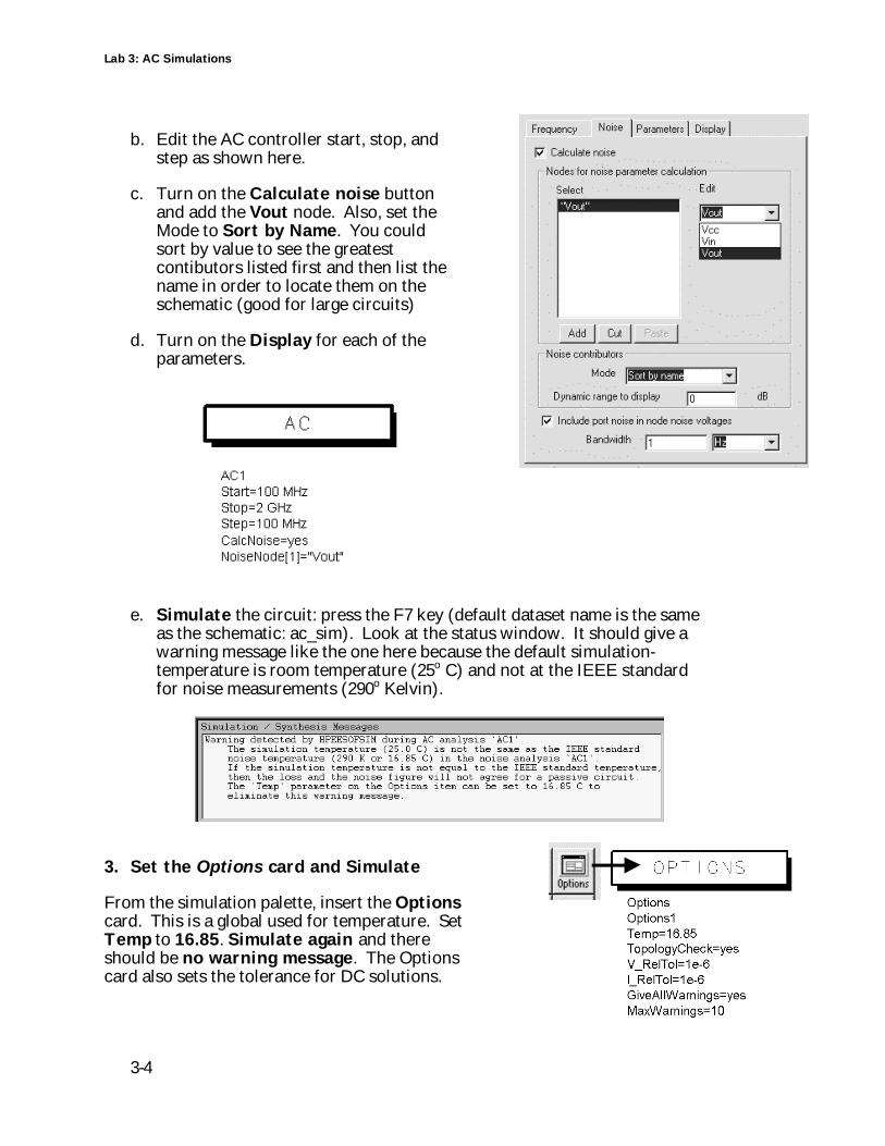
b. Edit the AC controller start, stop, andstep as shown here.
c. Turn on the Calculate noise buttonand add the Vout node. Also, set theMode to Sort by Name. You couldsort by value to see the greatestcontibutors listed first and then list thename in order to locate them on theschematic (good for large circuits)
d. Turn on the Display for each of theparameters.
e. Simulate the circuit: press the F7 key (default dataset name is the sameas the schematic: ac_sim). Look at the status window. It should give awarning message like the one here because the default simulation-temperature is room temperature (25o C) and not at the IEEE standardfor noise measurements (290o Kelvin).
3. Set the Options card and Simulate
From the simulation palette, insert the Optionscard. This is a global used for temperature. SetTemp to 16.85. Simulate again and thereshould be no warning message. The Optionscard also sets the tolerance for DC solutions.
Lab 3: AC Simulations
3-5
4. Display the noise data
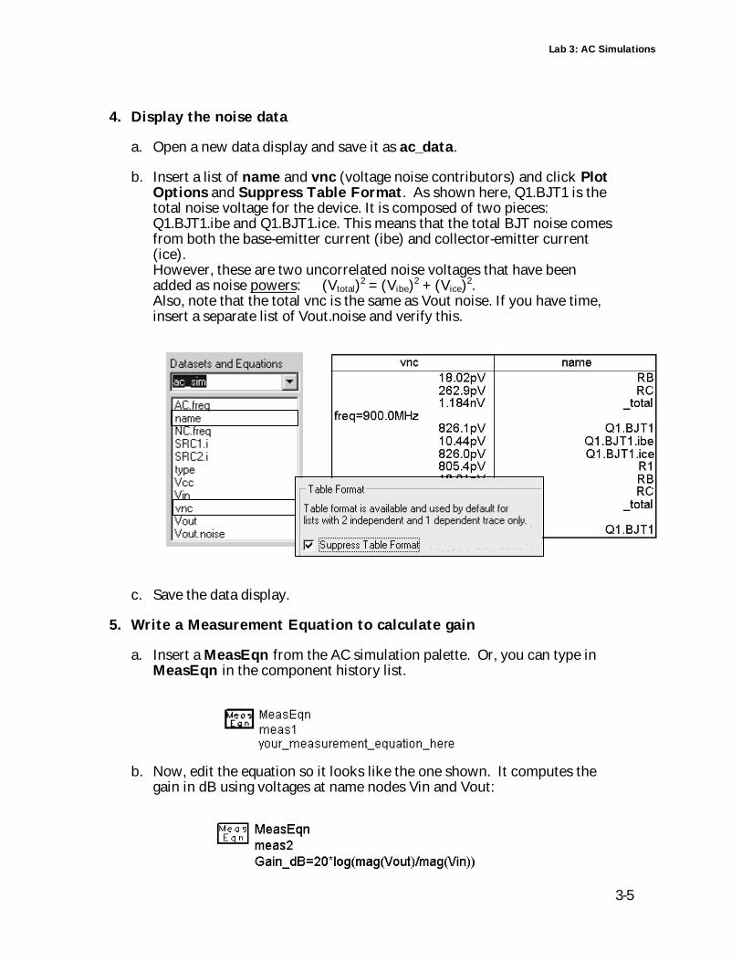
a. Open a new data display and save it as ac_data.
b. Insert a list of name and vnc (voltage noise contributors) and click PlotOptions and Suppress Table Format. As shown here, Q1.BJT1 is thetotal noise voltage for the device. It is composed of two pieces:Q1.BJT1.ibe and Q1.BJT1.ice. This means that the total BJT noise comesfrom both the base-emitter current (ibe) and collector-emitter current(ice).However, these are two uncorrelated noise voltages that have beenadded as noise powers: (Vtotal)2 = (Vibe)2 + (Vice)2.Also, note that the total vnc is the same as Vout noise. If you have time,insert a separate list of Vout.noise and verify this.
c. Save the data display.
5. Write a Measurement Equation to calculate gain
a. Insert a MeasEqn from the AC simulation palette. Or, you can type inMeasEqn in the component history list.
b. Now, edit the equation so it looks like the one shown. It computes thegain in dB using voltages at name nodes Vin and Vout:
Lab 3: AC Simulations
3-6
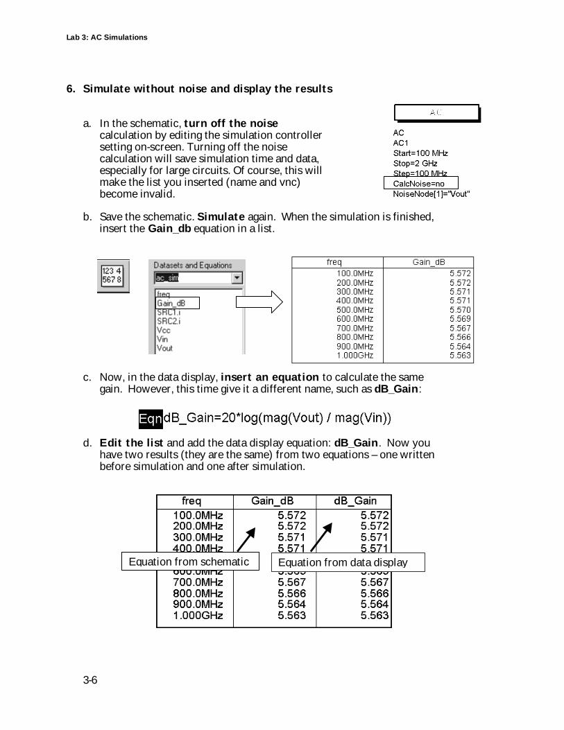
6. Simulate without noise and display the results
a. In the schematic, turn off the noisecalculation by editing the simulation controllersetting on-screen. Turning off the noisecalculation will save simulation time and data,especially for large circuits. Of course, this willmake the list you inserted (name and vnc)become invalid.
b. Save the schematic. Simulate again. When the simulation is finished,insert the Gain_db equation in a list.
c. Now, in the data display, insert an equation to calculate the samegain. However, this time give it a different name, such as dB_Gain:
d. Edit the list and add the data display equation: dB_Gain. Now youhave two results (they are the same) from two equations – one writtenbefore simulation and one after simulation.
Equation from schematic Equation from data displaydispdisplaydisplay
Lab 3: AC Simulations
3-7
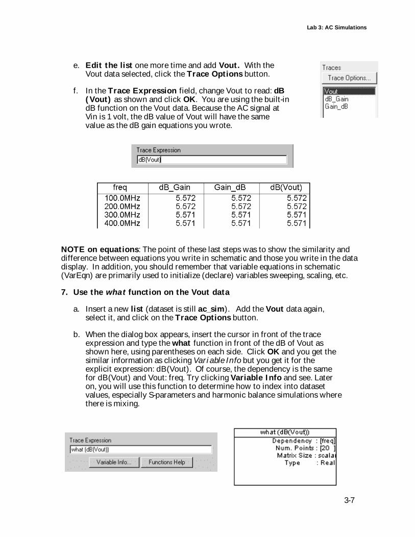
e. Edit the list one more time and add Vout. With theVout data selected, click the Trace Options button.
f. In the Trace Expression field, change Vout to read: dB(Vout) as shown and click OK. You are using the built-indB function on the Vout data. Because the AC signal atVin is 1 volt, the dB value of Vout will have the samevalue as the dB gain equations you wrote.
NOTE on equations: The point of these last steps was to show the similarity anddifference between equations you write in schematic and those you write in the datadisplay. In addition, you should remember that variable equations in schematic(VarEqn) are primarily used to initialize (declare) variables sweeping, scaling, etc.
7. Use the what function on the Vout data
a. Insert a new list (dataset is still ac_sim). Add the Vout data again,select it, and click on the Trace Options button.
b. When the dialog box appears, insert the cursor in front of the traceexpression and type the what function in front of the dB of Vout asshown here, using parentheses on each side. Click OK and you get thesimilar information as clicking Variable Info but you get it for theexplicit expression: dB(Vout). Of course, the dependency is the samefor dB(Vout) and Vout: freq. Try clicking Variable Info and see. Lateron, you will use this function to determine how to index into datasetvalues, especially S-parameters and harmonic balance simulations wherethere is mixing.
Lab 3: AC Simulations
3-8
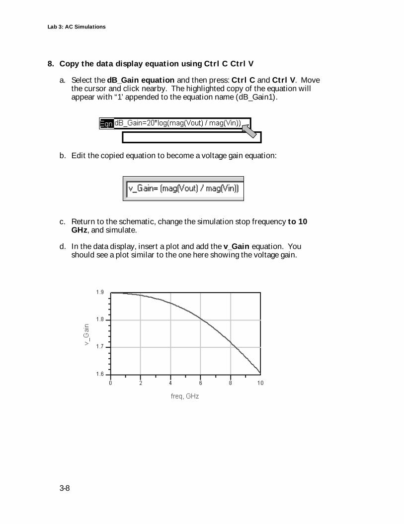
8. Copy the data display equation using Ctrl C Ctrl V
a. Select the dB_Gain equation and then press: Ctrl C and Ctrl V. Movethe cursor and click nearby. The highlighted copy of the equation willappear with “1’ appended to the equation name (dB_Gain1).
b. Edit the copied equation to become a voltage gain equation:
c. Return to the schematic, change the simulation stop frequency to 10GHz, and simulate.
d. In the data display, insert a plot and add the v_Gain equation. Youshould see a plot similar to the one here showing the voltage gain.
Lab 3: AC Simulations
3-9
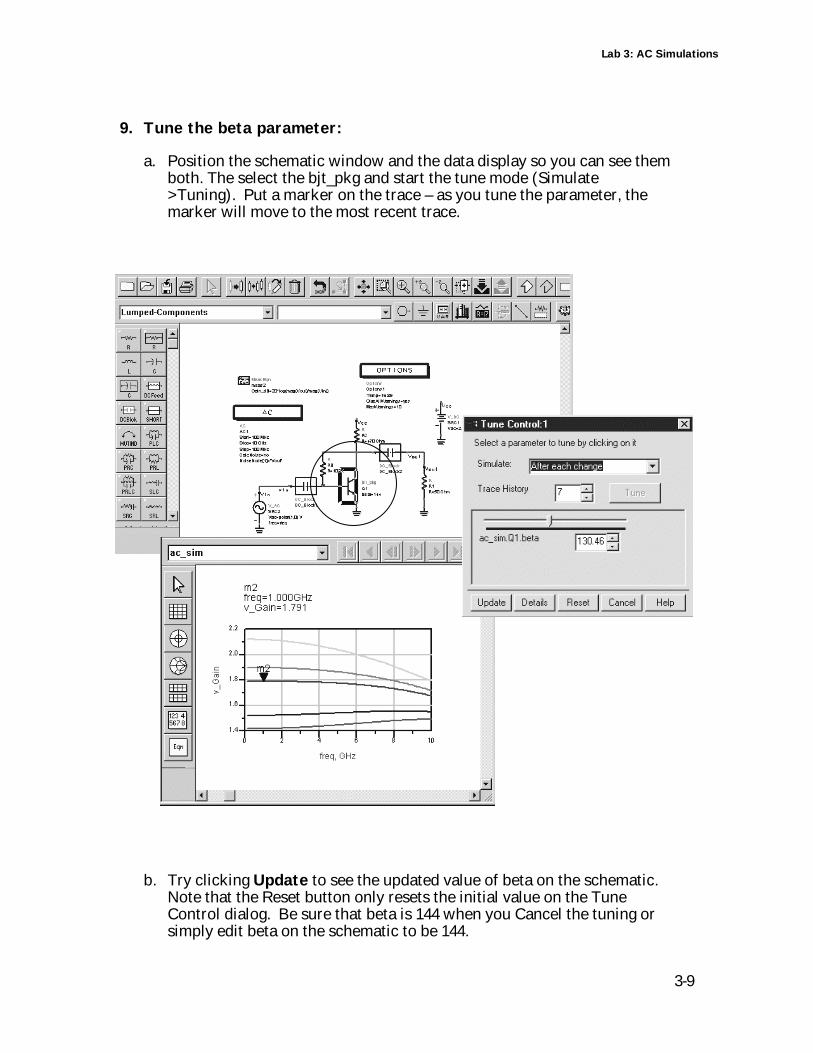
9. Tune the beta parameter:
a. Position the schematic window and the data display so you can see themboth. The select the bjt_pkg and start the tune mode (Simulate>Tuning). Put a marker on the trace – as you tune the parameter, themarker will move to the most recent trace.
b. Try clicking Update to see the updated value of beta on the schematic.Note that the Reset button only resets the initial value on the TuneControl dialog. Be sure that beta is 144 when you Cancel the tuning orsimply edit beta on the schematic to be 144.
Lab 3: AC Simulations
3-10
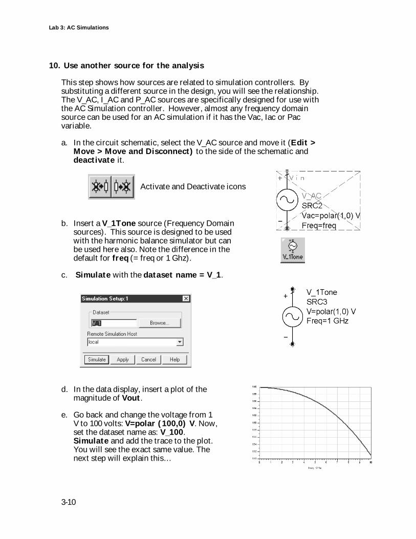
10. Use another source for the analysis
This step shows how sources are related to simulation controllers. Bysubstituting a different source in the design, you will see the relationship.The V_AC, I_AC and P_AC sources are specifically designed for use withthe AC Simulation controller. However, almost any frequency domainsource can be used for an AC simulation if it has the Vac, Iac or Pacvariable.
a. In the circuit schematic, select the V_AC source and move it (Edit >Move > Move and Disconnect) to the side of the schematic anddeactivate it.
b. Insert a V_1Tone source (Frequency Domainsources). This source is designed to be usedwith the harmonic balance simulator but canbe used here also. Note the difference in thedefault for freq (= freq or 1 Ghz).
c. Simulate with the dataset name = V_1.
d. In the data display, insert a plot of themagnitude of Vout.
e. Go back and change the voltage from 1V to 100 volts: V=polar (100,0) V. Now,set the dataset name as: V_100.Simulate and add the trace to the plot.You will see the exact same value. Thenext step will explain this…
Activate and Deactivate icons
Lab 3: AC Simulations
3-11
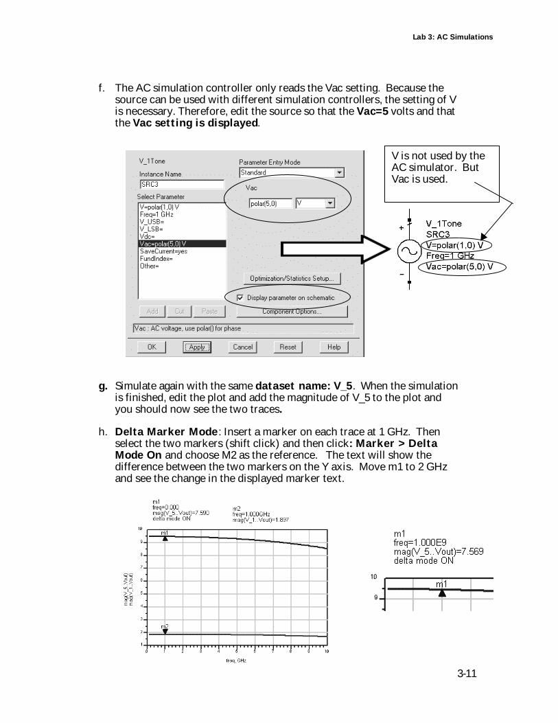
f. The AC simulation controller only reads the Vac setting. Because thesource can be used with different simulation controllers, the setting of Vis necessary. Therefore, edit the source so that the Vac=5 volts and thatthe Vac setting is displayed.
g. Simulate again with the same dataset name: V_5. When the simulationis finished, edit the plot and add the magnitude of V_5 to the plot andyou should now see the two traces.
h. Delta Marker Mode: Insert a marker on each trace at 1 GHz. Thenselect the two markers (shift click) and then click: Marker > DeltaMode On and choose M2 as the reference. The text will show thedifference between the two markers on the Y axis. Move m1 to 2 GHzand see the change in the displayed marker text.
V is not used by theAC simulator. ButVac is used.

Lab 3: AC Simulations
3-12
11. Sweep Vcc (as if the battery voltage dropped below 2 volts)
This step will require you to use the skills you already learned in this lab andin lab 2. You will set up a parameter sweep for Vdc from 1.8 to 2 volts in0.05 volt steps.
a. Replace the V_1Tone source with a V_AC source and deactivate theV_1Tone – use the command Edit > Move > Move and Disconnectand Edit > Component > Deactivate.
b. Insert a VAR (variable equation)initializing Vbias = 2 volts.
c. Redefine Vcc: Vdc = Vbias.
d. Insert a Parameter Sweep. Then set the SweepVar(sweep variable) to be Vbias, and be sure theSimulation Instance Name of the AC simulationcontroller is also set.
e. Simulate as ac_bat_swp (dataset name) and thendisplay the magnitude of the Vout data as shown.
12. Save all your work andclose the windows
Simulated battery drain overbroad frequency range. Also,Trace Options used to thickenthe trace lines.
Lab 3: AC Simulations
3-13
EXTRA EXERCISES:
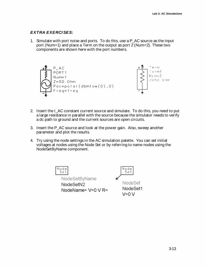
1. Simulate with port noise and ports. To do this, use a P_AC source as the inputport (Num=1) and place a Term on the output as port 2 (Num=2). These twocomponents are shown here with the port numbers.
2. Insert the I_AC constant current source and simulate. To do this, you need to puta large resistance in parallel with the source because the simulator needs to verifya dc path to ground and the current sources are open circuits.
3. Insert the P_AC source and look at the power gain. Also, sweep anotherparameter and plot the results.
4. Try using the node settings in the AC simulation palette. You can set initialvoltages at nodes using the Node Set or by referring to name nodes using theNodeSetByName component.

Lab 3: AC Simulations
3-14
THIS PAGE LEFT INTENTIONALLY BLANK
4
This chapter shows how to make S-parameter simulations andhow to determine matching network values.
Lab 4: S-parameter Simulations
Lab 4: S-parameter Simulations
4-2
OBJECTIVES• Measure gain and impedance with S-parameters
• Use a sweep plans, parameter sweeps, and equation based impedances
• Plot and manipulate data in new ways
About this lab: This lab continues the mixer testing by making various S-parameter
measurements to determine circuit performance: gain and impedance.
PROCEDURE
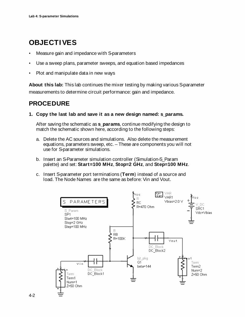
1. Copy the last lab and save it as a new design named: s_params.
After saving the schematic as s_params, continue modifying the design tomatch the schematic shown here, according to the following steps:
a. Delete the AC sources and simulations. Also delete the measurementequations, parameters sweep, etc. – These are components you will notuse for S-parameter simulations.
b. Insert an S-Parameter simulation controller (Simulation-S_Parampalette) and set: Start=100 MHz, Stop=2 GHz, and Step=100 MHz.
c. Insert S-parameter port terminations (Term) instead of a source andload. The Node Names are the same as before: Vin and Vout.
Lab 4: S-parameter Simulations
4-3
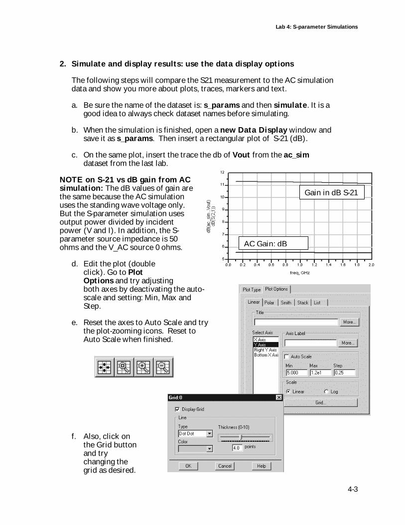
2. Simulate and display results: use the data display options
The following steps will compare the S21 measurement to the AC simulationdata and show you more about plots, traces, markers and text.
a. Be sure the name of the dataset is: s_params and then simulate. It is agood idea to always check dataset names before simulating.
b. When the simulation is finished, open a new Data Display window andsave it as s_params. Then insert a rectangular plot of S-21 (dB).
c. On the same plot, insert the trace the db of Vout from the ac_simdataset from the last lab.
NOTE on S-21 vs dB gain from ACsimulation: The dB values of gain arethe same because the AC simulationuses the standing wave voltage only.But the S-parameter simulation usesoutput power divided by incidentpower (V and I). In addition, the S-parameter source impedance is 50ohms and the V_AC source 0 ohms.
d. Edit the plot (doubleclick). Go to PlotOptions and try adjustingboth axes by deactivating the auto-scale and setting: Min, Max andStep.
e. Reset the axes to Auto Scale and trythe plot-zooming icons. Reset toAuto Scale when finished.
f. Also, click onthe Grid buttonand trychanging thegrid as desired.
Gain in dB S-21
AC Gain: dB

Lab 4: S-parameter Simulations
4-4
You may want to use these features later.
Lab 4: S-parameter Simulations
4-5
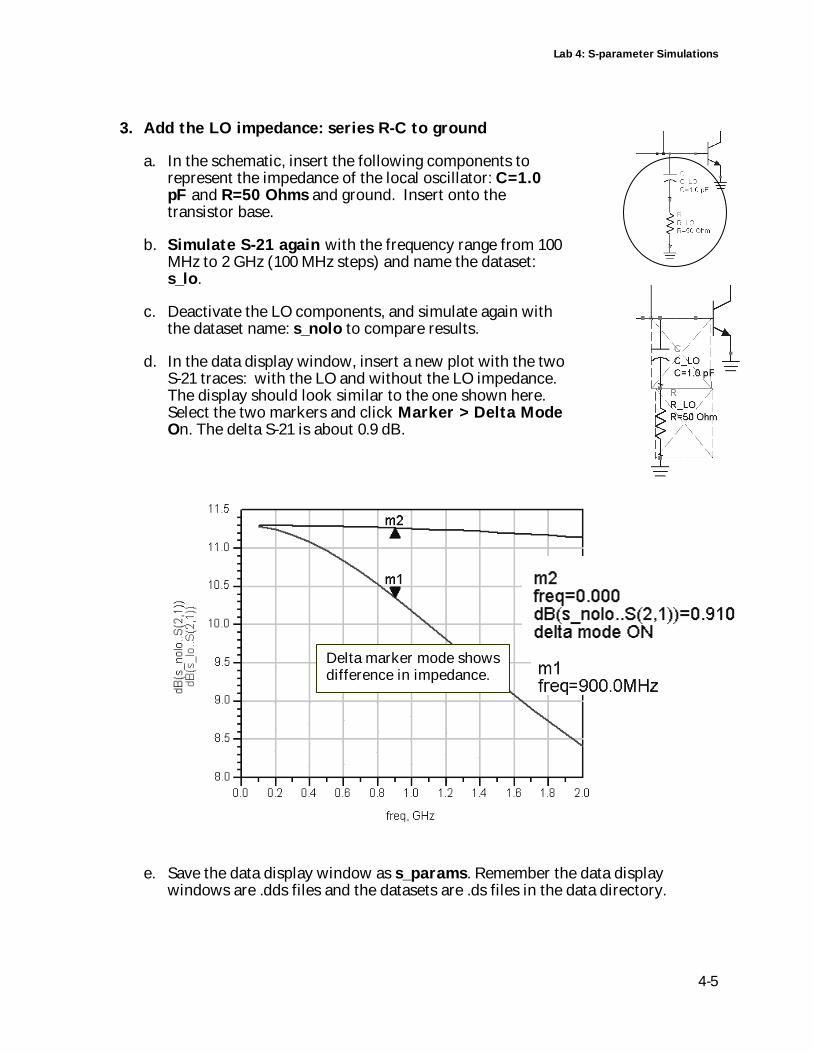
3. Add the LO impedance: series R-C to ground
a. In the schematic, insert the following components torepresent the impedance of the local oscillator: C=1.0pF and R=50 Ohms and ground. Insert onto thetransistor base.
b. Simulate S-21 again with the frequency range from 100MHz to 2 GHz (100 MHz steps) and name the dataset:s_lo.
c. Deactivate the LO components, and simulate again withthe dataset name: s_nolo to compare results.
d. In the data display window, insert a new plot with the twoS-21 traces: with the LO and without the LO impedance.The display should look similar to the one shown here.Select the two markers and click Marker > Delta ModeOn. The delta S-21 is about 0.9 dB.
e. Save the data display window as s_params. Remember the data displaywindows are .dds files and the datasets are .ds files in the data directory.
Delta marker mode showsdifference in impedance.
Lab 4: S-parameter Simulations
4-6
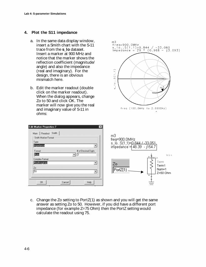
4. Plot the S11 impedance
a. In the same data display window,insert a Smith chart with the S-11trace from the s_lo dataset.Insert a marker at 900 MHz andnotice that the marker shows thereflection coefficient (magnitude/angle) and also the impedance(real and imaginary). For thedesign, there is an obviousmismatch here.
b. Edit the marker readout (doubleclick on the marker readout).When the dialog appears, changeZo to 50 and click OK. Themarker will now give you the realand imaginary value of S-11 inohms:
c. Change the Zo setting to PortZ(1) as shown and you will get the sameanswer as setting Zo to 50. However, if you did have a different portimpedance (for example Z=75 Ohm) then the PortZ setting wouldcalculate the readout using 75.
Lab 4: S-parameter Simulations
4-7
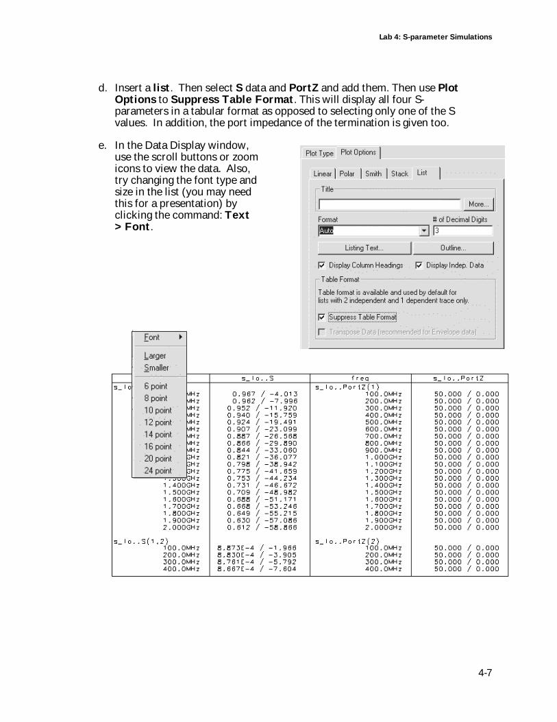
d. Insert a list. Then select S data and PortZ and add them. Then use PlotOptions to Suppress Table Format. This will display all four S-parameters in a tabular format as opposed to selecting only one of the Svalues. In addition, the port impedance of the termination is given too.
e. In the Data Display window,use the scroll buttons or zoomicons to view the data. Also,try changing the font type andsize in the list (you may needthis for a presentation) byclicking the command: Text> Font.
Lab 4: S-parameter Simulations
4-8
5. Add frequency sensitive terminations for the RF & IF
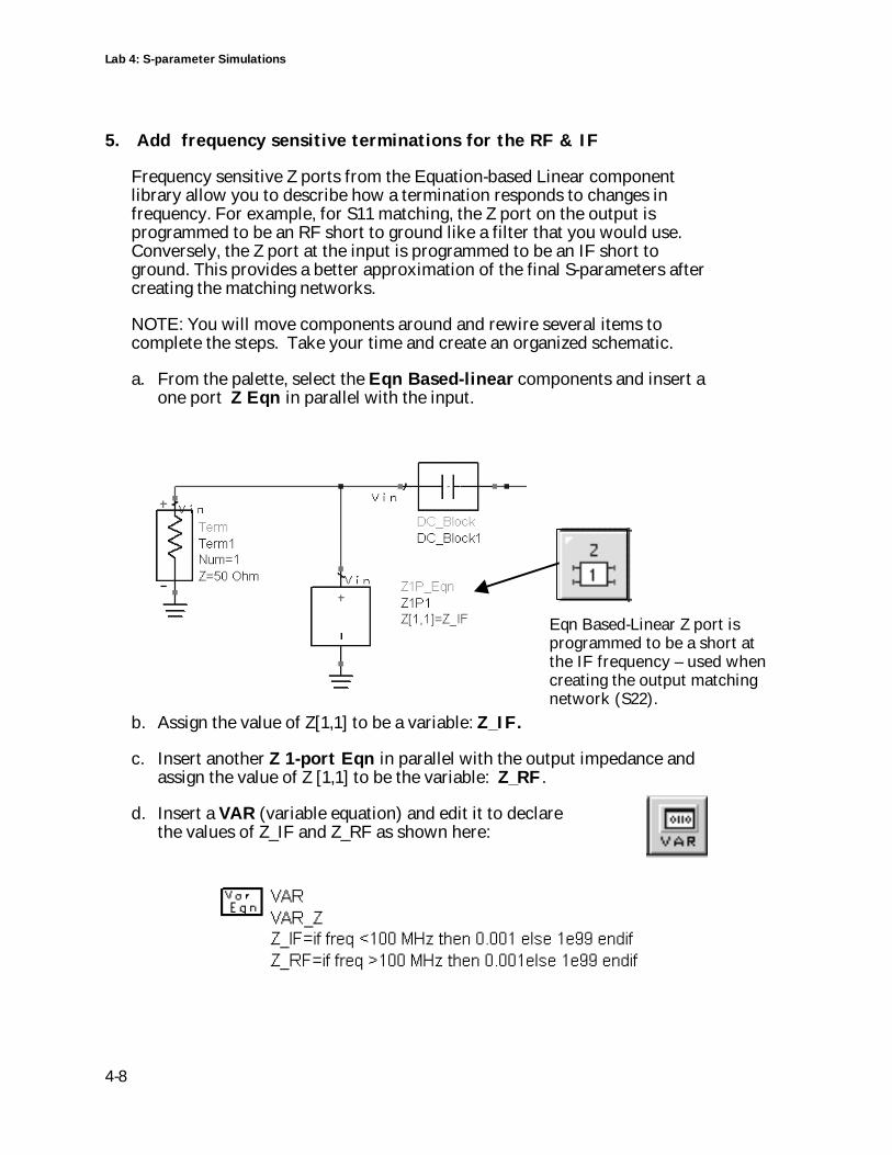
Frequency sensitive Z ports from the Equation-based Linear componentlibrary allow you to describe how a termination responds to changes infrequency. For example, for S11 matching, the Z port on the output isprogrammed to be an RF short to ground like a filter that you would use.Conversely, the Z port at the input is programmed to be an IF short toground. This provides a better approximation of the final S-parameters aftercreating the matching networks.
NOTE: You will move components around and rewire several items tocomplete the steps. Take your time and create an organized schematic.
a. From the palette, select the Eqn Based-linear components and insert aone port Z Eqn in parallel with the input.
b. Assign the value of Z[1,1] to be a variable: Z_IF.
c. Insert another Z 1-port Eqn in parallel with the output impedance andassign the value of Z [1,1] to be the variable: Z_RF.
d. Insert a VAR (variable equation) and edit it to declarethe values of Z_IF and Z_RF as shown here:
Eqn Based-Linear Z port isprogrammed to be a short atthe IF frequency – used whencreating the output matchingnetwork (S22).
Lab 4: S-parameter Simulations
4-9
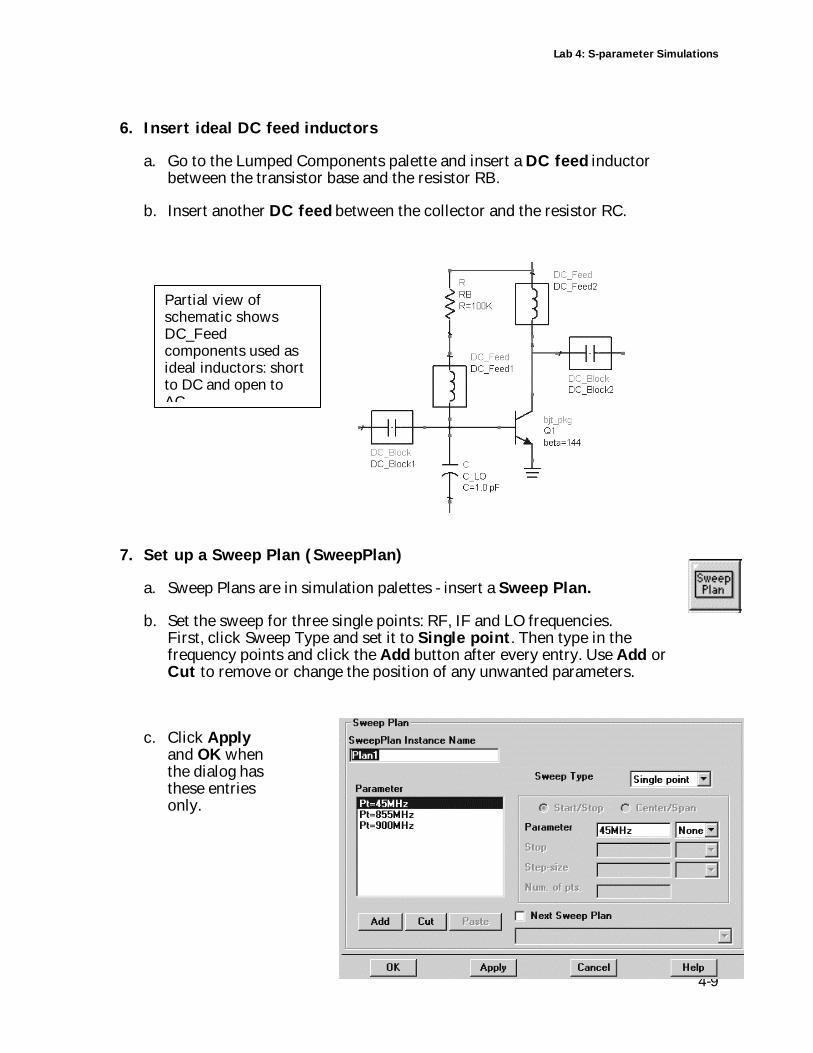
6. Insert ideal DC feed inductors
a. Go to the Lumped Components palette and insert a DC feed inductorbetween the transistor base and the resistor RB.
b. Insert another DC feed between the collector and the resistor RC.
7. Set up a Sweep Plan (SweepPlan)
a. Sweep Plans are in simulation palettes - insert a Sweep Plan.
b. Set the sweep for three single points: RF, IF and LO frequencies.First, click Sweep Type and set it to Single point. Then type in thefrequency points and click the Add button after every entry. Use Add orCut to remove or change the position of any unwanted parameters.
c. Click Applyand OK whenthe dialog hasthese entriesonly.
Partial view ofschematic showsDC_Feedcomponents used asideal inductors: shortto DC and open toAC.
Lab 4: S-parameter Simulations
4-10
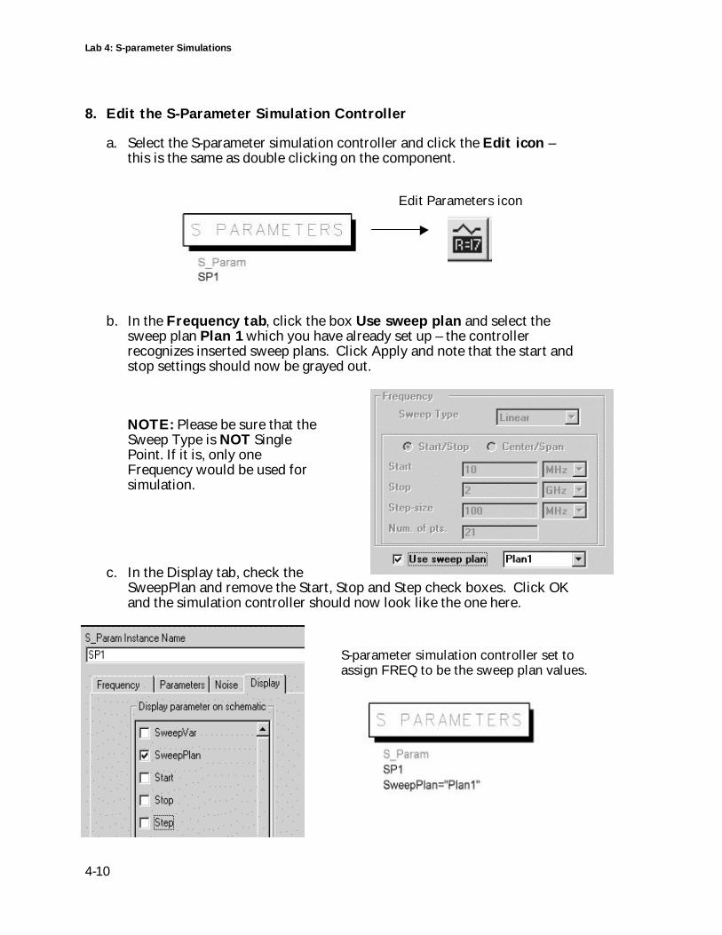
8. Edit the S-Parameter Simulation Controller
a. Select the S-parameter simulation controller and click the Edit icon –this is the same as double clicking on the component.
b. In the Frequency tab, click the box Use sweep plan and select thesweep plan Plan 1 which you have already set up – the controllerrecognizes inserted sweep plans. Click Apply and note that the start andstop settings should now be grayed out.
NOTE: Please be sure that theSweep Type is NOT SinglePoint. If it is, only oneFrequency would be used forsimulation.
c. In the Display tab, check theSweepPlan and remove the Start, Stop and Step check boxes. Click OKand the simulation controller should now look like the one here.
S-parameter simulation controller set toassign FREQ to be the sweep plan values.
Edit Parameters icon
Lab 4: S-parameter Simulations
4-11
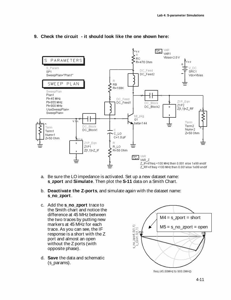
9. Check the circuit - it should look like the one shown here:
a. Be sure the LO impedance is activated. Set up a new dataset name:s_zport and Simulate. Then plot the S-11 data on a Smith Chart.
b. Deactivate the Z-ports, and simulate again with the dataset name:s_no_zport.
c. Add the s_no_zport trace tothe Smith chart and notice thedifference at 45 MHz betweenthe two traces by putting newmarkers at 45 MHz for eachtrace. As you can see, the IFresponse is a short with the Zport and almost an openwithout the Z ports (withopposite phase).
d. Save the data and schematic(s_params).
M4 = s_zport = short
M5 = s_no_zport = open
Lab 4: S-parameter Simulations
4-12
10. Modify the BJT_PKG sub-circuit (B-C capacitance)
The following steps will further demonstrate the use of Z ports, sub-circuits andsimulations in the hierarchy.
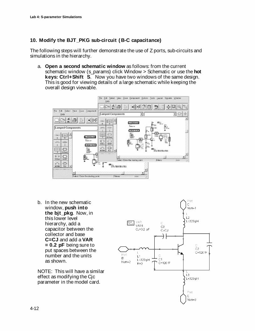
a. Open a second schematic window as follows: from the currentschematic window (s_params) click Window > Schematic or use the hotkeys: Ctrl+Shift S. Now you have two windows of the same design.This is good for viewing details of a large schematic while keeping theoverall design viewable.
b. In the new schematicwindow, push intothe bjt_pkg. Now, inthis lower levelhierarchy, add acapacitor between thecollector and baseC=CJ and add a VAR= 0.2 pF being sure toput spaces between thenumber and the unitsas shown.
NOTE: This will have a similareffect as modifying the Cjcparameter in the model card.
Lab 4: S-parameter Simulations
4-13
c. At this lower level, press the F7 simulate key. You should get an errormessage in the status window because there is no simulation controller.
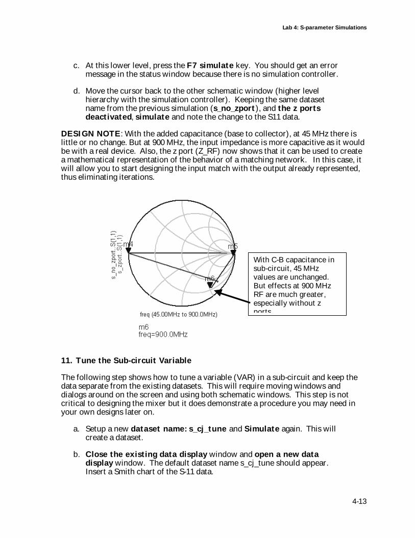
d. Move the cursor back to the other schematic window (higher levelhierarchy with the simulation controller). Keeping the same datasetname from the previous simulation (s_no_zport), and the z portsdeactivated, simulate and note the change to the S11 data.
DESIGN NOTE: With the added capacitance (base to collector), at 45 MHz there islittle or no change. But at 900 MHz, the input impedance is more capacitive as it wouldbe with a real device. Also, the z port (Z_RF) now shows that it can be used to createa mathematical representation of the behavior of a matching network. In this case, itwill allow you to start designing the input match with the output already represented,thus eliminating iterations.
11. Tune the Sub-circuit Variable
The following step shows how to tune a variable (VAR) in a sub-circuit and keep thedata separate from the existing datasets. This will require moving windows anddialogs around on the screen and using both schematic windows. This step is notcritical to designing the mixer but it does demonstrate a procedure you may need inyour own designs later on.
a. Setup a new dataset name: s_cj_tune and Simulate again. This willcreate a dataset.
b. Close the existing data display window and open a new datadisplay window. The default dataset name s_cj_tune should appear.Insert a Smith chart of the S-11 data.
With C-B capacitance insub-circuit, 45 MHzvalues are unchanged.But effects at 900 MHzRF are much greater,especially without zports.

Lab 4: S-parameter Simulations
4-14
c. In the upper level schematic,start the Tune mode(Simulate> Tuning). You willsee the status window and theTune control dialog appear.Next, move the cursor back tothe bjt_pkg sub-circuitwindow and select the CJparameter value.
d. Position the data displaywindow so you can see thenew trace values resultingfrom the tuning. Here is acase where small changesoccur and so you can zoominto the Smith chart.
e. To easily end tuning, press thekeyboard Esc key or use theright mouse button EndCommand.
f. Delete the Smith chart so the data display is empty.
g. In the subcircuit: remove the Capacitor and VarEqn.
NOTE: Save the s_params design. It will be used for the next lab to developthe final input and output matching networks for the mixer.
Lab 4: S-parameter Simulations
4-15
NOTE on the next 2 steps: Do these only if you have time. They are not requiredfor the mixer design. They demonstrate how to write or read data into ADS.
12. Reading and Writing S-parameter Data with an S2P file
You can read or write data in Touchstone, MDIF, or Citifile formats. ADScan convert supported data into the ADS dataset format. Typically, thesedata files are put in the project directory but they can also be sent to thedata directory. You can control where they reside.
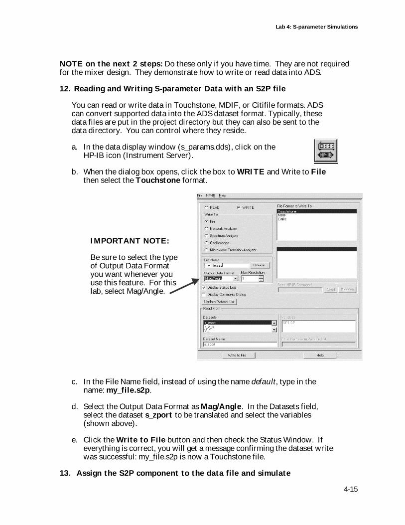
a. In the data display window (s_params.dds), click on theHP-IB icon (Instrument Server).
b. When the dialog box opens, click the box to WRITE and Write to Filethen select the Touchstone format.
c. In the File Name field, instead of using the name default, type in thename: my_file.s2p.
d. Select the Output Data Format as Mag/Angle. In the Datasets field,select the dataset s_zport to be translated and select the variables(shown above).
e. Click the Write to File button and then check the Status Window. Ifeverything is correct, you will get a message confirming the dataset writewas successful: my_file.s2p is now a Touchstone file.
13. Assign the S2P component to the data file and simulate
IMPORTANT NOTE:
Be sure to select the typeof Output Data Formatyou want whenever youuse this feature. For thislab, select Mag/Angle.
Lab 4: S-parameter Simulations
4-16
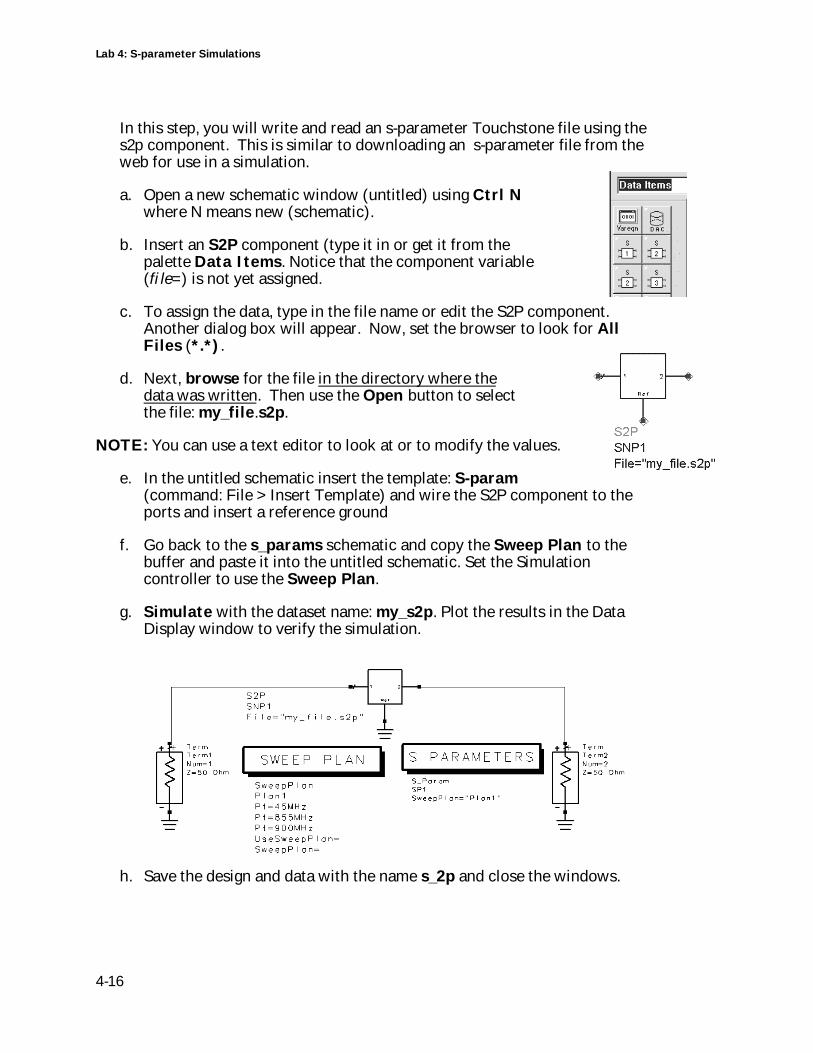
In this step, you will write and read an s-parameter Touchstone file using thes2p component. This is similar to downloading an s-parameter file from theweb for use in a simulation.
a. Open a new schematic window (untitled) using Ctrl Nwhere N means new (schematic).
b. Insert an S2P component (type it in or get it from thepalette Data Items. Notice that the component variable(file=) is not yet assigned.
c. To assign the data, type in the file name or edit the S2P component.Another dialog box will appear. Now, set the browser to look for AllFiles (*.*).
d. Next, browse for the file in the directory where thedata was written. Then use the Open button to selectthe file: my_file.s2p.
NOTE: You can use a text editor to look at or to modify the values.
e. In the untitled schematic insert the template: S-param(command: File > Insert Template) and wire the S2P component to theports and insert a reference ground
f. Go back to the s_params schematic and copy the Sweep Plan to thebuffer and paste it into the untitled schematic. Set the Simulationcontroller to use the Sweep Plan.
g. Simulate with the dataset name: my_s2p. Plot the results in the DataDisplay window to verify the simulation.
h. Save the design and data with the name s_2p and close the windows.
Lab 4: S-parameter Simulations
4-17
EXTRA EXERCISES:
1. Translate data from a Touchstone file into a dataset. Use the Instrument Serverwindow and READ the file back into the data directory as an ADS dataset. Thensimulate the S2P component with another name and save the file.
2. Use a real library device and simulate both with and without the Z ports to actuallysee the difference in S11. For example, use a device from one of the BJT libraries.
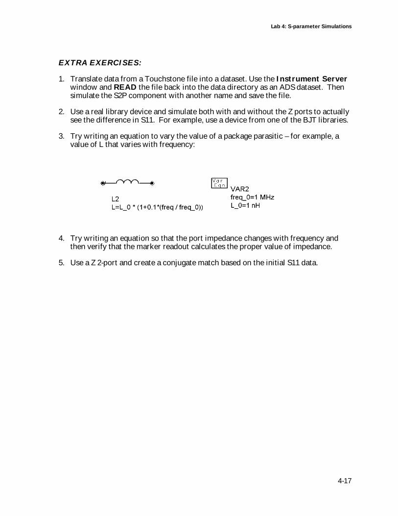
3. Try writing an equation to vary the value of a package parasitic – for example, avalue of L that varies with frequency:
4. Try writing an equation so that the port impedance changes with frequency andthen verify that the marker readout calculates the proper value of impedance.
5. Use a Z 2-port and create a conjugate match based on the initial S11 data.

5
This chapter shows various ways of creating matching networksby sweeping values and using optimization.
Lab 5: Matching & Optimization
Lab 5: Matching and Optimization
5-2
OBJECTIVES
• Create an input match to the RF and an output match to the IF
• Tune and Optimize to achieve matching goals
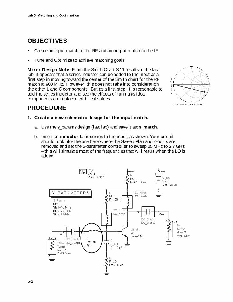
Mixer Design Note: From the Smith Chart S-11 results in the lastlab, it appears that a series inductor can be added to the input as afirst step in moving toward the center of the Smith chart for the RFmatch at 900 MHz. However, this does not take into considerationthe other L and C components. But as a first step, it is reasonable toadd the series inductor and see the effects of tuning as idealcomponents are replaced with real values.
PROCEDURE
1. Create a new schematic design for the input match.
a. Use the s_params design (last lab) and save it as: s_match.
b. Insert an inductor L in series to the input, as shown. Your circuitshould look like the one here where the Sweep Plan and Z-ports areremoved and set the S-parameter controller to sweep 15 MHz to 2.7 GHz– this will simulate most of the frequencies that will result when the LO isadded.
Lab 5: Matching and Optimization
5-3
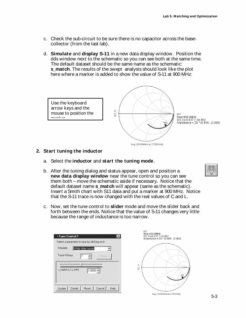
c. Check the sub-circuit to be sure there is no capacitor across the base-collector (from the last lab).
d. Simulate and display S-11 in a new data display window. Position thedds window next to the schematic so you can see both at the same time.The default dataset should be the same name as the schematic:s_match. The results of the swept analysis should look like the plothere where a marker is added to show the value of S-11 at 900 MHz:
2. Start tuning the inductor
a. Select the inductor and start the tuning mode.
b. After the tuning dialog and status appear, open and position anew data display window near the tune control so you can seethem both – move the schematic aside if necessary. Notice that thedefault dataset name s_match will appear (same as the schematic).Insert a Smith chart with S11 data and put a marker at 900 MHz. Noticethat the S-11 trace is now changed with the real values of C and L.
c. Now, set the tune control to slider mode and move the slider back andforth between the ends. Notice that the value of S-11 changes very littlebecause the range of inductance is too narrow.
Use the keyboardarrow keys and themouse to position themarker.
Lab 5: Matching and Optimization
5-4
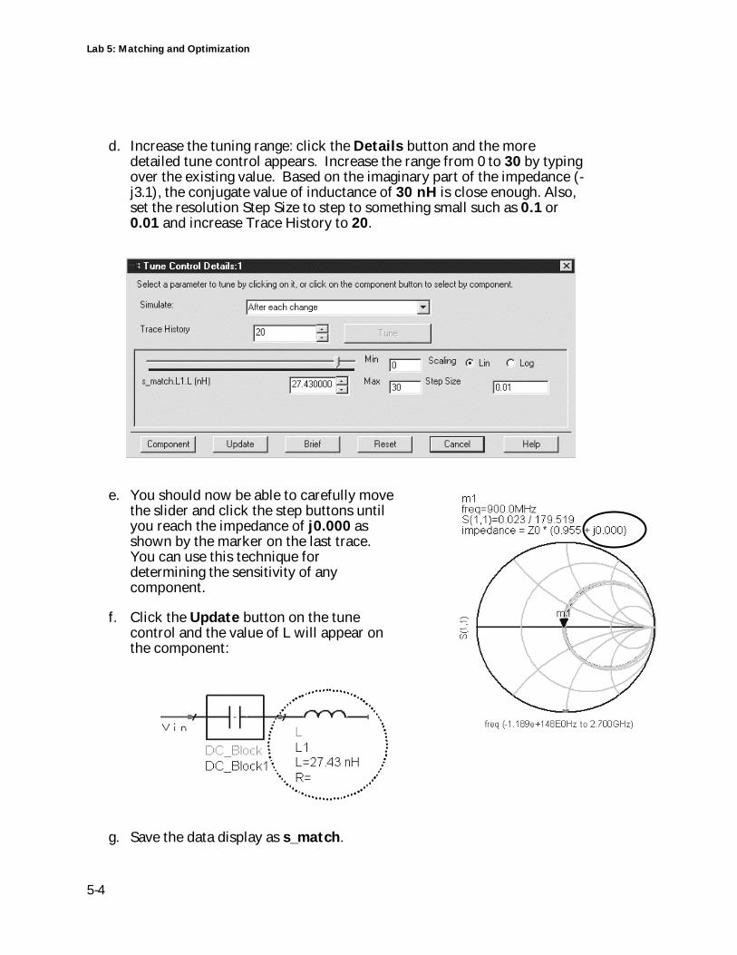
d. Increase the tuning range: click the Details button and the moredetailed tune control appears. Increase the range from 0 to 30 by typingover the existing value. Based on the imaginary part of the impedance (-j3.1), the conjugate value of inductance of 30 nH is close enough. Also,set the resolution Step Size to step to something small such as 0.1 or0.01 and increase Trace History to 20.
e. You should now be able to carefully movethe slider and click the step buttons untilyou reach the impedance of j0.000 asshown by the marker on the last trace.You can use this technique fordetermining the sensitivity of anycomponent.
f. Click the Update button on the tunecontrol and the value of L will appear onthe component:
g. Save the data display as s_match.
Lab 5: Matching and Optimization
5-5
3. Build a new input matching network (new configuration)
CIRCUIT DESIGN NOTE: At this point, the addition of the series inductor is only afirst approximation. The remaining ideal components ( DC feeds and blocks) must bereplaced by realistic values and this may require a completely different topology otherthan just adding a series inductance. Also, a shunt capacitor needs to be added to theinput to remove the IF signal that may appear there. Therefore, instead of continuingto add components in an attempt to create a match, you will use the followingconfiguration that will solve all the matching problems for the input. This will speedup the lab exercise.
a. On the input, remove the series inductor you just tuned. It will bereplaced by a network which will achieve the desired RF match and alsoprovide the filtering.
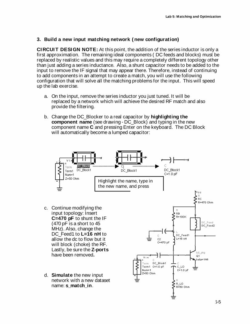
b. Change the DC_Blocker to a real capacitor by highlighting thecomponent name (see drawing - DC_Block) and typing in the newcomponent name C and pressing Enter on the keyboard. The DC Blockwill automatically become a lumped capacitor:
c. Continue modifying theinput topology: InsertC=470 pF to shunt the IF(470 pF is a short to 45MHz). Also, change theDC_Feed1 to L=16 nH toallow the dc to flow but itwill block (choke) the RF.Lastly, be sure the Z-portshave been removed.
d. Simulate the new inputnetwork with a new datasetname: s_match_in.
Highlight the name, type inthe new name, and pressEnter. omponent by typing
Lab 5: Matching and Optimization
5-6
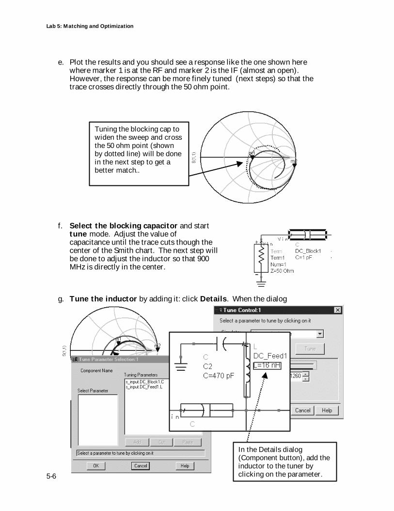
e. Plot the results and you should see a response like the one shown herewhere marker 1 is at the RF and marker 2 is the IF (almost an open).However, the response can be more finely tuned (next steps) so that thetrace crosses directly through the 50 ohm point.
f. Select the blocking capacitor and starttune mode. Adjust the value ofcapacitance until the trace cuts though thecenter of the Smith chart. The next step willbe done to adjust the inductor so that 900MHz is directly in the center.
g. Tune the inductor by adding it: click Details. When the dialog
Tuning the blocking cap towiden the sweep and crossthe 50 ohm point (shownby dotted line) will be donein the next step to get abetter match..
Tuning produces trace cuttingthrough desired impedance. Nextstep: tune L to decrease inputinductance and maker should be atdesired point.
In the Details dialog(Component button), add theinductor to the tuner byclicking on the parameter.
Lab 5: Matching and Optimization
5-7
appears, select the Component Button and add the inductor byclicking on the parameter value (not the component) L=16 nH.
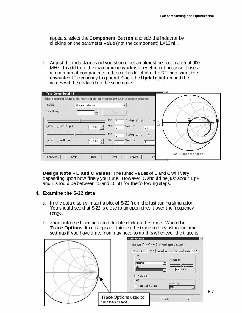
h. Adjust the inductance and you should get an almost perfect match at 900MHz. In addition, the matching network is very efficient because it usesa minimum of components to block the dc, choke the RF, and shunt theunwanted IF frequency to ground. Click the Update button and thevalues will be updated on the schematic.
Design Note – L and C values: The tuned values of L and C will varydepending upon how finely you tune. However, C should be just about 1 pFand L should be between 15 and 16 nH for the following steps.
4. Examine the S-22 data
a. In the data display, insert a plot of S-22 from the last tuning simulation.You should see that S-22 is close to an open circuit over the frequencyrange.
b. Zoom into the trace area and double click on the trace. When theTrace Options dialog appears, thicken the trace and try using the othersettings if you have time. You may need to do this whenever the trace is
Trace Options used tothicken trace.
Lab 5: Matching and Optimization
5-8
difficult to see or when it is in a very narrow range. Build the outputcircuit.
Output Match Design Note: For the next part of the lab exercise, you will use theoptimizer to achieve the output match with a given topology.
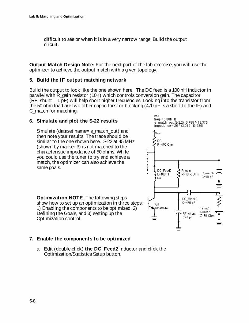
5. Build the IF output matching network
Build the output to look like the one shown here. The DC feed is a 100 nH inductor inparallel with R_gain resistor (10K) which controls conversion gain. The capacitor(RF_shunt = 1 pF) will help short higher frequencies. Looking into the transistor fromthe 50 ohm load are two other capacitors for blocking (470 pF is a short to the IF) andC_match for matching.
6. Simulate and plot the S-22 results
Simulate (dataset name= s_match_out) andthen note your results. The trace should besimilar to the one shown here. S-22 at 45 MHz(shown by marker 3) is not matched to thecharacteristic impedance of 50 ohms. Whileyou could use the tuner to try and achieve amatch, the optimizer can also achieve thesame goals.
Optimization NOTE: The following stepsshow how to set up an optimization in three steps:1) Enabling the components to be optimized, 2)Defining the Goals, and 3) setting up theOptimization control.
7. Enable the components to be optimized
a. Edit (double click) the DC_Feed2 inductor and click theOptimization/Statistics Setup button.
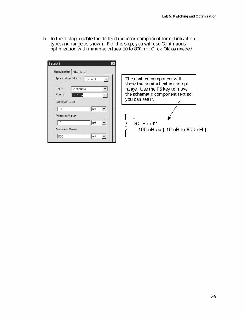
Lab 5: Matching and Optimization
5-9
b. In the dialog, enable the dc feed inductor component for optimization,type, and range as shown. For this step, you will use Continuousoptimization with min/max values: 10 to 800 nH. Click OK as needed.
The enabled component willshow the nominal value and optrange. Use the F5 key to movethe schematic component text soyou can see it.
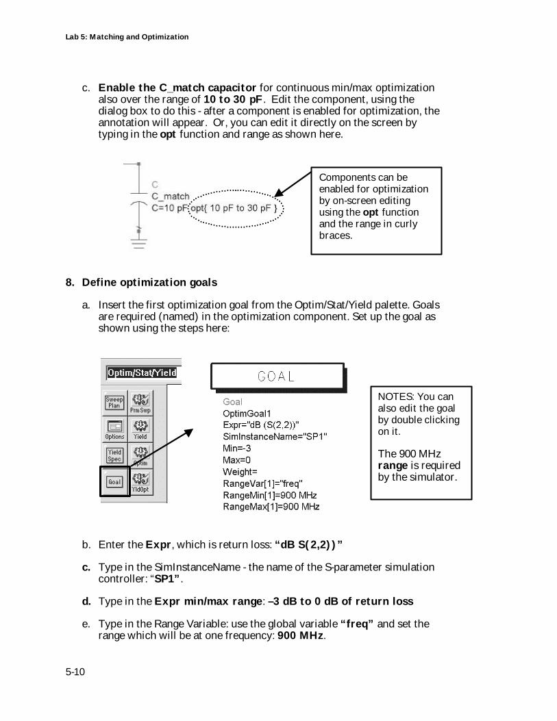
Lab 5: Matching and Optimization
5-10
c. Enable the C_match capacitor for continuous min/max optimizationalso over the range of 10 to 30 pF. Edit the component, using thedialog box to do this - after a component is enabled for optimization, theannotation will appear. Or, you can edit it directly on the screen bytyping in the opt function and range as shown here.
8. Define optimization goals
a. Insert the first optimization goal from the Optim/Stat/Yield palette. Goalsare required (named) in the optimization component. Set up the goal asshown using the steps here:
b. Enter the Expr, which is return loss: “dB S(2,2))”
c. Type in the SimInstanceName - the name of the S-parameter simulationcontroller: “SP1”.
d. Type in the Expr min/max range: –3 dB to 0 dB of return loss
e. Type in the Range Variable: use the global variable “freq” and set therange which will be at one frequency: 900 MHz.
Components can beenabled for optimizationby on-screen editingusing the opt functionand the range in curlybraces.
NOTES: You canalso edit the goalby double clickingon it.
The 900 MHzrange is requiredby the simulator.
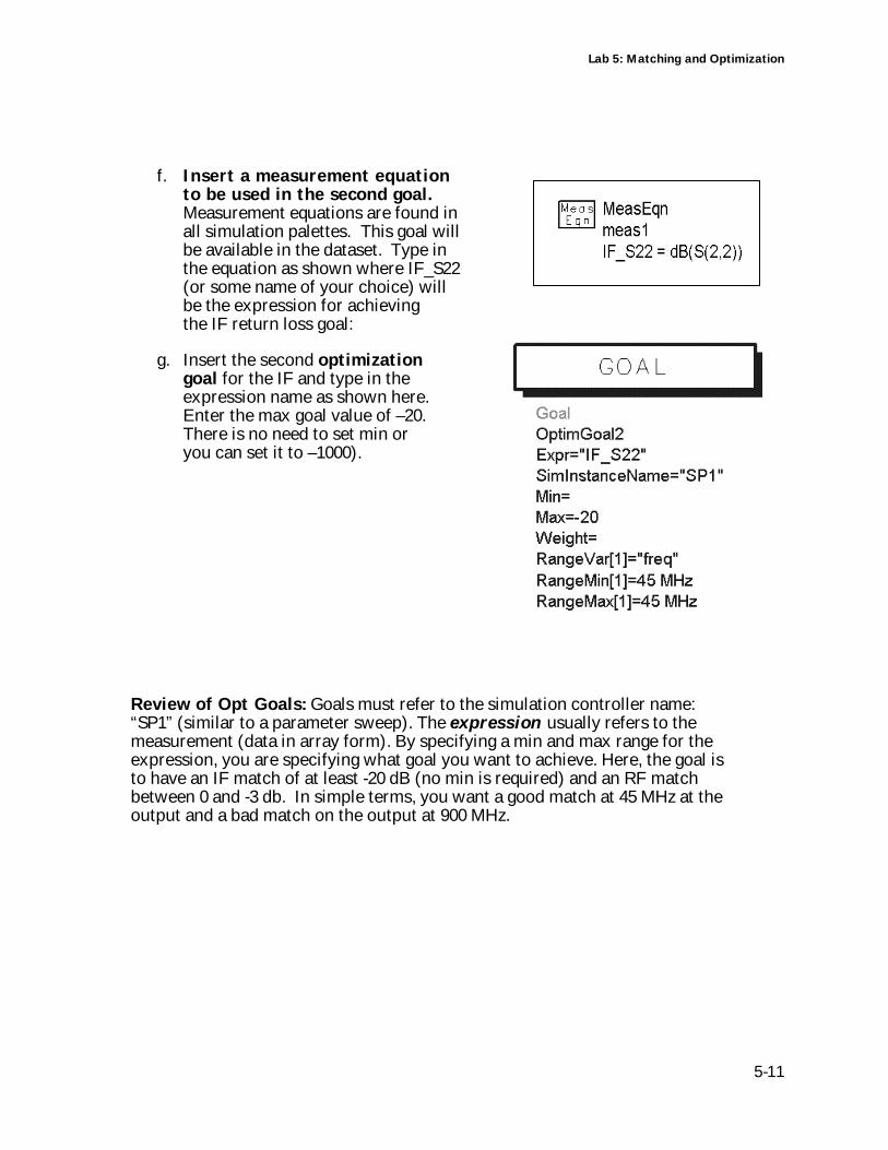
Lab 5: Matching and Optimization
5-11
f. Insert a measurement equationto be used in the second goal.Measurement equations are found inall simulation palettes. This goal willbe available in the dataset. Type inthe equation as shown where IF_S22(or some name of your choice) willbe the expression for achievingthe IF return loss goal:
g. Insert the second optimizationgoal for the IF and type in theexpression name as shown here.Enter the max goal value of –20.There is no need to set min oryou can set it to –1000).
Review of Opt Goals: Goals must refer to the simulation controller name:“SP1” (similar to a parameter sweep). The expression usually refers to themeasurement (data in array form). By specifying a min and max range for theexpression, you are specifying what goal you want to achieve. Here, the goal isto have an IF match of at least -20 dB (no min is required) and an RF matchbetween 0 and -3 db. In simple terms, you want a good match at 45 MHz at theoutput and a bad match on the output at 900 MHz.
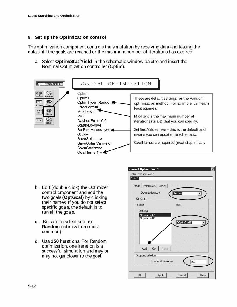
Lab 5: Matching and Optimization
5-12
9. Set up the Optimization control
The optimization component controls the simulation by receiving data and testing thedata until the goals are reached or the maximum number of iterations has expired.
a. Select Optim/Stat/Yield in the schematic window palette and insert theNominal Optimization controller (Optim).
b. Edit (double click) the Optimizercontrol cmponent and add thetwo goals (OptGoal) by clickingtheir names. If you do not selectspecific goals, the default is torun all the goals.
c. Be sure to select and useRandom optimization (mostcommon).
d. Use 150 iterations. For Randomoptimization, one iteration is asuccessful simulation and may ormay not get closer to the goal.
These are default settings for the Randomoptimization method. For example, L2 meansleast squares.
MaxIters is the maximum number ofiterations (trials) that you can specify.
SetBestValues=yes – this is the default andmeans you can update the schematic.
GoalNames are required (next step in lab).
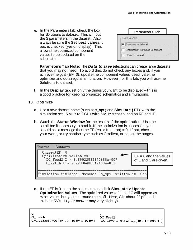
Lab 5: Matching and Optimization
5-13
e. In the Parameters tab, check the boxfor Solutions to dataset. This will putthe S parameters in the dataset. Also,always be sure the Set best values…box is checked (yes on display). Thisallows the optimized componentvalues to be updated on theschematic.
Parameters Tab Note: The Data to save selections can create large datasetsthat you may not need. To avoid this, do not check any boxes and, if youachieve the goal (EF=0), update the component values, deactivate theoptimizer and do a regular simulation. However, for this lab, you will use theSolutions to dataset.
f. In the Display tab, set only the things you want to be displayed – this isa good practice for keeping organized schematics and simulations.
10. Optimize
a. Use a new dataset name (such as s_opt) and Simulate (F7) with thesimulation set 15 MHz to 2 GHz with 5 MHz steps to land on RF and IF.
b. Watch the Status Window for the results of the optimization. Use thescroll bar if necessary to read it. If the optimization is successful, youshould see a message that the EF (error function) = 0. If not, checkyour work, or try another type such as Gradient, or adjust the ranges.
c. If the EF is 0, go to the schematic and click Simulate > UpdateOptimization Values. The optimized values of L and C will appear asexact values but you can round them off. Here, C is about 22 pF and Lis about 560 nH (your answer may vary slightly).
Parameters Tab
EF = 0 and the valuesof L and C are given.
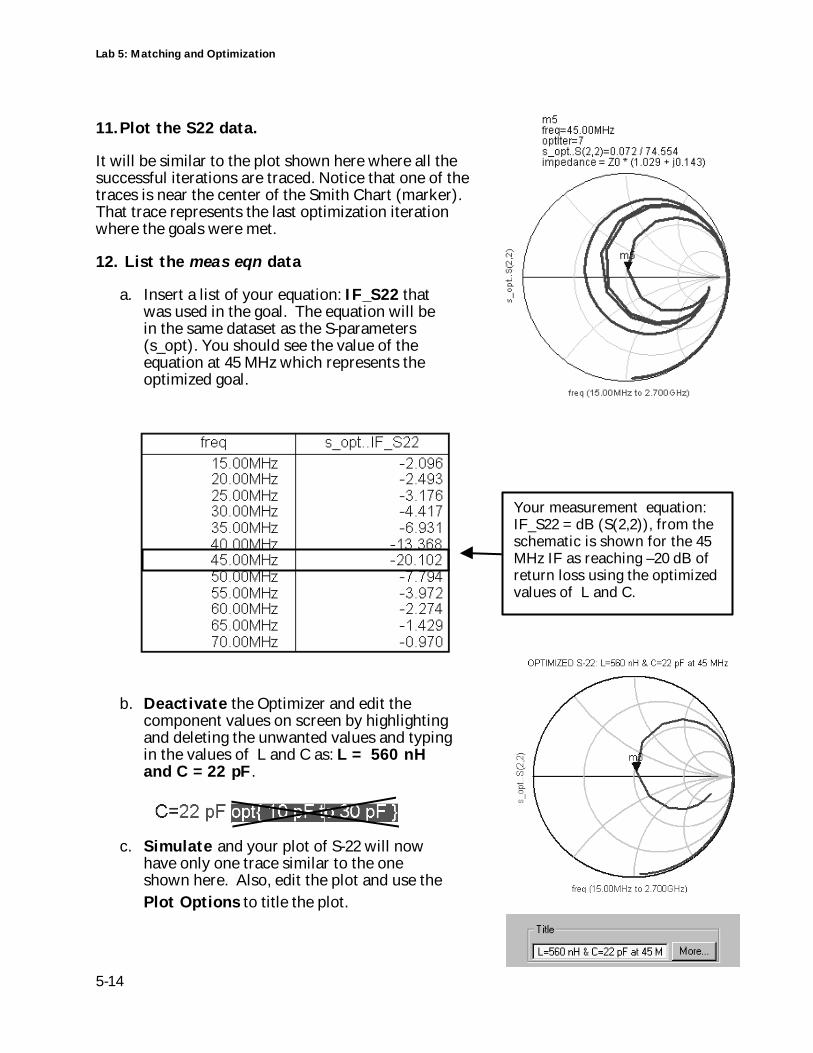
Lab 5: Matching and Optimization
5-14
11. Plot the S22 data.
It will be similar to the plot shown here where all thesuccessful iterations are traced. Notice that one of thetraces is near the center of the Smith Chart (marker).That trace represents the last optimization iterationwhere the goals were met.
12. List the meas eqn data
a. Insert a list of your equation: IF_S22 thatwas used in the goal. The equation will bein the same dataset as the S-parameters(s_opt). You should see the value of theequation at 45 MHz which represents theoptimized goal.
b. Deactivate the Optimizer and edit thecomponent values on screen by highlightingand deleting the unwanted values and typingin the values of L and C as: L = 560 nHand C = 22 pF.
c. Simulate and your plot of S-22 will nowhave only one trace similar to the oneshown here. Also, edit the plot and use thePlot Options to title the plot.
Your measurement equation:IF_S22 = dB (S(2,2)), from theschematic is shown for the 45MHz IF as reaching –20 dB ofreturn loss using the optimizedvalues of L and C.
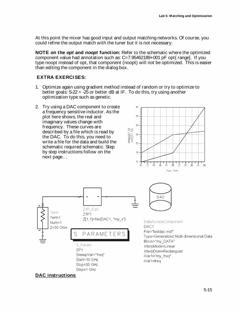
Lab 5: Matching and Optimization
5-15
At this point the mixer has good input and output matching networks. Of course, youcould refine the output match with the tuner but it is not necessary.
NOTE on the opt and noopt function: Refer to the schematic where the optimizedcomponent value had annotation such as: C=7.95462189+001 pF opt{ range]. If youtype noopt instead of opt, that component (noopt) will not be optimized. This is easierthan editing the component in the dialog box.
EXTRA EXERCISES:
1. Optimize again using gradient method instead of random or try to optimize tobetter goals: S-22 = -25 or better dB at IF. To do this, try using anotheroptimization type such as genetic.
2. Try using a DAC component to createa frequency sensitive inductor. As theplot here shows, the real andimaginary values change withfrequency. These curves aredescribed by a file which is read bythe DAC. To do this, you need towrite a file for the data and build theschematic required schematic. Stepby step instructions follow on thenext page…
DAC instructions:
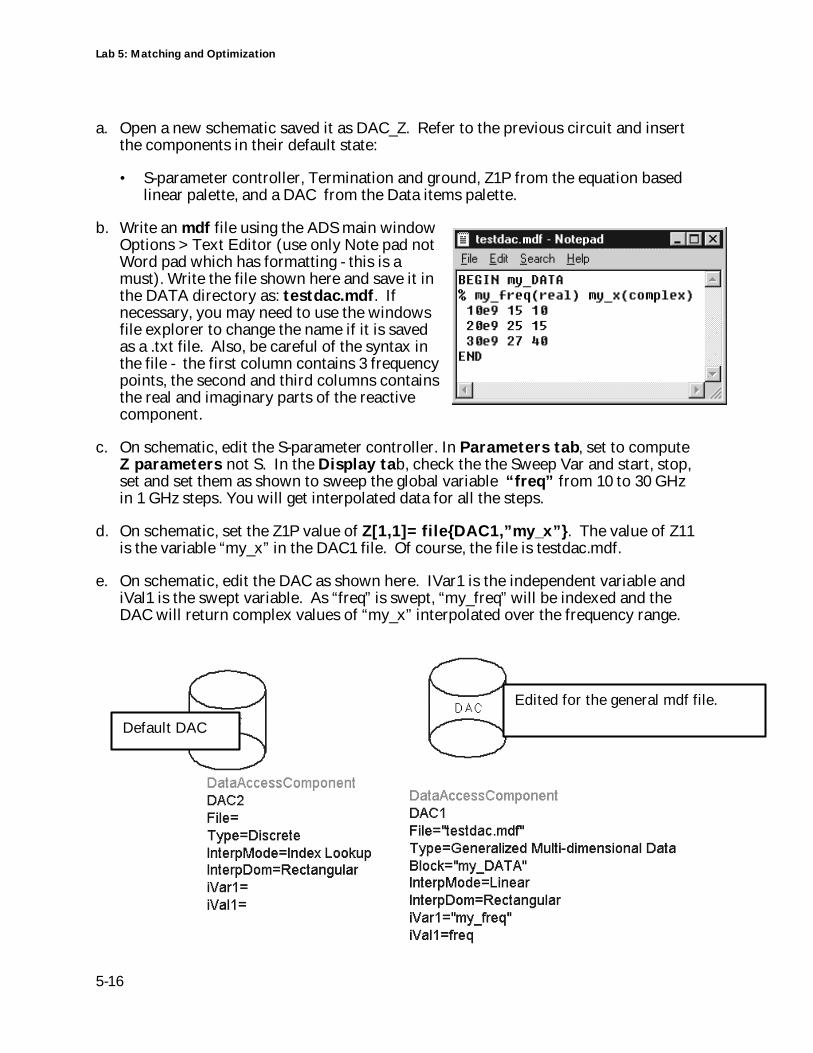
Lab 5: Matching and Optimization
5-16
a. Open a new schematic saved it as DAC_Z. Refer to the previous circuit and insertthe components in their default state:
• S-parameter controller, Termination and ground, Z1P from the equation basedlinear palette, and a DAC from the Data items palette.
b. Write an mdf file using the ADS main windowOptions > Text Editor (use only Note pad notWord pad which has formatting - this is amust). Write the file shown here and save it inthe DATA directory as: testdac.mdf. Ifnecessary, you may need to use the windowsfile explorer to change the name if it is savedas a .txt file. Also, be careful of the syntax inthe file - the first column contains 3 frequencypoints, the second and third columns containsthe real and imaginary parts of the reactivecomponent.
c. On schematic, edit the S-parameter controller. In Parameters tab, set to computeZ parameters not S. In the Display tab, check the the Sweep Var and start, stop,set and set them as shown to sweep the global variable “freq” from 10 to 30 GHzin 1 GHz steps. You will get interpolated data for all the steps.
d. On schematic, set the Z1P value of Z[1,1]= file{DAC1,”my_x”}. The value of Z11is the variable “my_x” in the DAC1 file. Of course, the file is testdac.mdf.
e. On schematic, edit the DAC as shown here. IVar1 is the independent variable andiVal1 is the swept variable. As “freq” is swept, “my_freq” will be indexed and theDAC will return complex values of “my_x” interpolated over the frequency range.
Default DAC
Edited for the general mdf file.
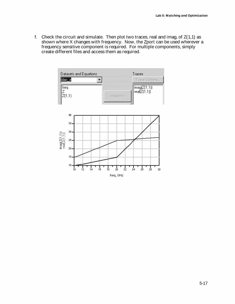
Lab 5: Matching and Optimization
5-17
f. Check the circuit and simulate. Then plot two traces, real and imag, of Z(1,1) asshown where X changes with frequency. Now, the Zport can be used wherever afrequency sensitive component is required. For multiple components, simplycreate different files and access them as required.

Lab 5: Matching and Optimization
5-18
THIS PAGE IS INTENTIONALLY BLANK

6
This chapter shows the fundamentals of using the HarmonicBalance simulator to look at the output spectrum, gaincompression, and other measurements. Also, the E-Syn tool isused to build a filter for the mixer.
Lab 6: Harmonic Balance Mixer
Simulations and E-Syn
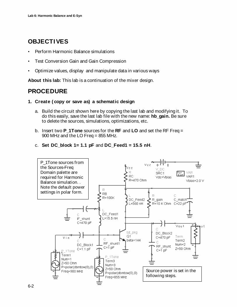
Lab 6: Harmonic Balance and E-Syn
6-2
OBJECTIVES
• Perform Harmonic Balance simulations
• Test Conversion Gain and Gain Compression
• Optimize values, display and manipulate data in various ways
About this lab: This lab is a continuation of the mixer design.
PROCEDURE
1. Create (copy or save as) a schematic design
a. Build the circuit shown here by copying the last lab and modifying it. Todo this easily, save the last lab file with the new name: hb_gain. Be sureto delete the sources, simulations, optimizations, etc.
b. Insert two P_1Tone sources for the RF and LO and set the RF Freq =900 MHz and the LO Freq = 855 MHz.
c. Set DC_block 1= 1.1 pF and DC_Feed1 = 15.5 nH.
P_1Tone sources fromthe Sources-FreqDomain palette arerequired for HarmonicBalance simulation. .Note the default powersettings in polar form.
Source power is set in thefollowing steps.
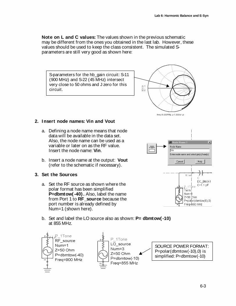
Lab 6: Harmonic Balance and E-Syn
6-3
Note on L and C values: The values shown in the previous schematicmay be different from the ones you obtained in the last lab. However, thesevalues should be used to keep the class consistent. The simulated S-parameters are still very good as shown here:
2. Insert node names: Vin and Vout
a. Defining a node name means that nodedata will be available in the data set.Also, the node name can be used as avariable or later on as the RF value.Insert the node name: Vin.
b. Insert a node name at the output: Vout(refer to the schematic if necessary).
3. Set the Sources
a. Set the RF source as shown where thepolar format has been simplifiedP=dbmtow(-40). Also, label the namefrom Port 1 to RF_source because theport number is already defined byNum=1 (shown here).
b. Set and label the LO source also as shown: P= dbmtow(-10)at 855 MHz.
S-parameters for the hb_gain circuit: S-11(900 MHz) and S-22 (45 MHz) intersectvery close to 50 ohms and J zero for thiscircuit.
SOURCE POWER FORMAT:P=polar(dbmtow(-10),0) issimplified: P=dbmtow(-10)
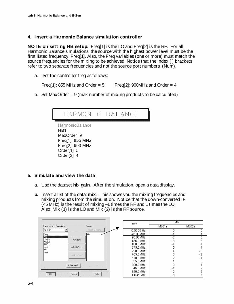
Lab 6: Harmonic Balance and E-Syn
6-4
4. Insert a Harmonic Balance simulation controller
NOTE on setting HB setup: Freq[1] is the LO and Freq[2] is the RF. For allHarmonic Balance simulations, the source with the highest power level must be thefirst listed frequency: Freq[1]. Also, the Freq variables (one or more) must match thesource frequencies for the mixing to be achieved. Notice that the index [ ] bracketsrefer to two separate frequencies and not the source port numbers (Num).
a. Set the controller freq as follows:
Freq[1]: 855 MHz and Order = 5 Freq[2]: 900MHz and Order = 4.
b. Set MaxOrder = 9 (max number of mixing products to be calculated)
5. Simulate and view the data
a. Use the dataset hb_gain. After the simulation, open a data display.
b. Insert a list of the data: mix. This shows you the mixing frequencies andmixing products from the simulation. Notice that the down-converted IF(45 MHz) is the result of mixing –1 times the RF and 1 times the LO.Also, Mix (1) is the LO and Mix (2) is the RF source.
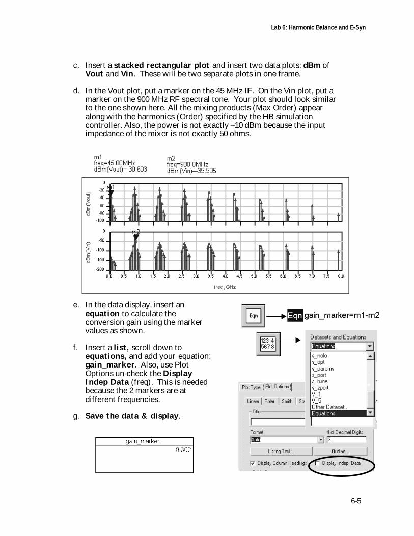
Lab 6: Harmonic Balance and E-Syn
6-5
c. Insert a stacked rectangular plot and insert two data plots: dBm ofVout and Vin. These will be two separate plots in one frame.
d. In the Vout plot, put a marker on the 45 MHz IF. On the Vin plot, put amarker on the 900 MHz RF spectral tone. Your plot should look similarto the one shown here. All the mixing products (Max Order) appearalong with the harmonics (Order) specified by the HB simulationcontroller. Also, the power is not exactly –10 dBm because the inputimpedance of the mixer is not exactly 50 ohms.
e. In the data display, insert anequation to calculate theconversion gain using the markervalues as shown.
f. Insert a list, scroll down toequations, and add your equation:gain_marker. Also, use PlotOptions un-check the DisplayIndep Data (freq). This is neededbecause the 2 markers are atdifferent frequencies.
g. Save the data & display.

Lab 6: Harmonic Balance and E-Syn
6-6
Design Note on gain: At this point, you have a good idea that the conversion gain isclose. However, this method of using markers is not completely accurate because thedBm values returned by the marker are only valid if the impedance of the system isexactly 50 ohms. This is because the dBm function assumes 50 ohms. In the nextsteps, you will refine the simulation setup, learn more about using the dBm functionand use a more accurate method of calculating gain.
6. Use variables instead of fixed values for Freq and Power
The next few steps show how to use variable instead of “hard coded” numbers in asimulation setup. This is important for more complex circuit refinement andcalculations in the remaining labs.
a. In the schematic, insert a variable equation from the Data Items paletteor, simply type VAR in the component history field and press Enter.
b. Edit the VAR and assign the variables as shown for LO, RF, and IFfrequency and power as shown. Assign the units (MHz) here and do notset the units anywhere else or they may multiply in the simulation.
c. Edit the sources and replace the values with the variables you justcreated for freq and power as shown:
d. Edit the Harmonic Balance controller as shown here. Notice that there isno MHz term required because it is already set in the VAR.
MaxOrder = number of mixingproducts calculated from Freqand Order:
Freq[1] is a variable or anumber. Order [1]=5 meansFreq[1] will be calculated with5 harmonics.
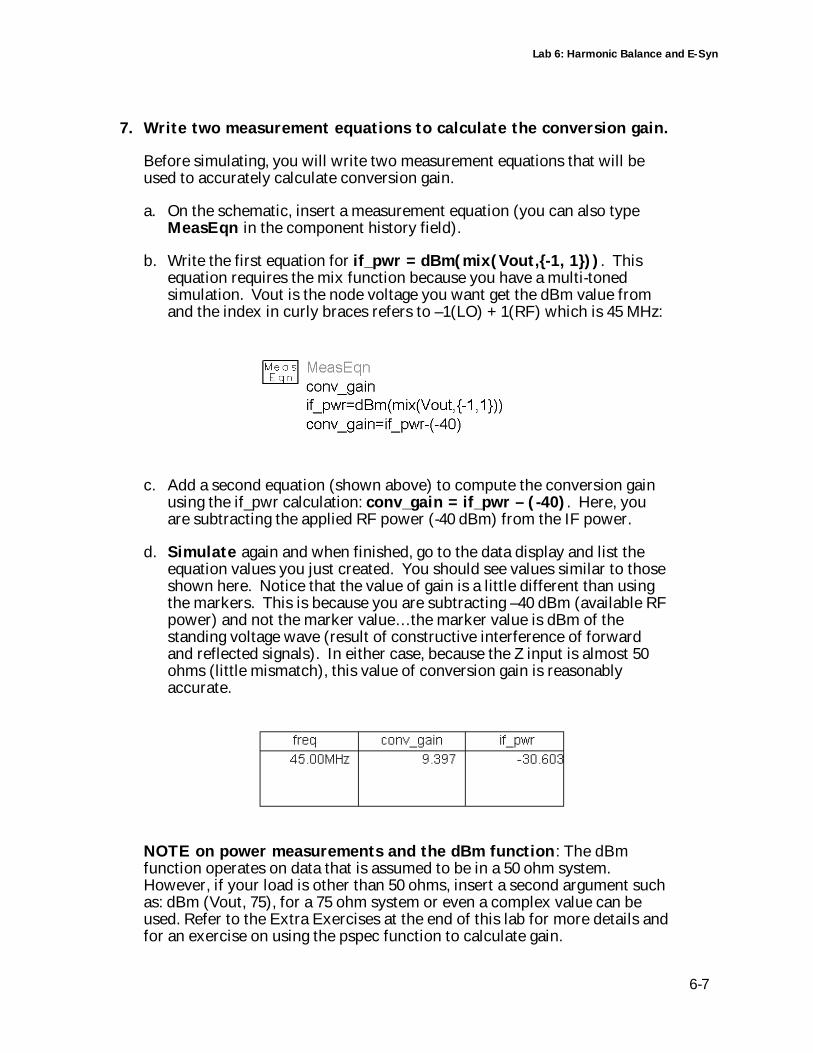
Lab 6: Harmonic Balance and E-Syn
6-7
7. Write two measurement equations to calculate the conversion gain.
Before simulating, you will write two measurement equations that will beused to accurately calculate conversion gain.
a. On the schematic, insert a measurement equation (you can also typeMeasEqn in the component history field).
b. Write the first equation for if_pwr = dBm(mix(Vout,{-1, 1})). Thisequation requires the mix function because you have a multi-tonedsimulation. Vout is the node voltage you want get the dBm value fromand the index in curly braces refers to –1(LO) + 1(RF) which is 45 MHz:
c. Add a second equation (shown above) to compute the conversion gainusing the if_pwr calculation: conv_gain = if_pwr – (-40). Here, youare subtracting the applied RF power (-40 dBm) from the IF power.
d. Simulate again and when finished, go to the data display and list theequation values you just created. You should see values similar to thoseshown here. Notice that the value of gain is a little different than usingthe markers. This is because you are subtracting –40 dBm (available RFpower) and not the marker value…the marker value is dBm of thestanding voltage wave (result of constructive interference of forwardand reflected signals). In either case, because the Z input is almost 50ohms (little mismatch), this value of conversion gain is reasonablyaccurate.
NOTE on power measurements and the dBm function: The dBmfunction operates on data that is assumed to be in a 50 ohm system.However, if your load is other than 50 ohms, insert a second argument suchas: dBm (Vout, 75), for a 75 ohm system or even a complex value can beused. Refer to the Extra Exercises at the end of this lab for more details andfor an exercise on using the pspec function to calculate gain.
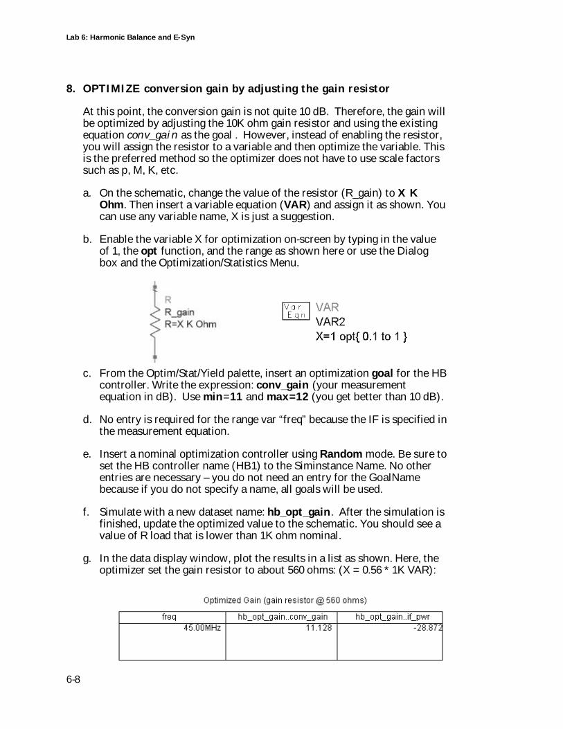
Lab 6: Harmonic Balance and E-Syn
6-8
8. OPTIMIZE conversion gain by adjusting the gain resistor
At this point, the conversion gain is not quite 10 dB. Therefore, the gain willbe optimized by adjusting the 10K ohm gain resistor and using the existingequation conv_gain as the goal . However, instead of enabling the resistor,you will assign the resistor to a variable and then optimize the variable. Thisis the preferred method so the optimizer does not have to use scale factorssuch as p, M, K, etc.
a. On the schematic, change the value of the resistor (R_gain) to X KOhm. Then insert a variable equation (VAR) and assign it as shown. Youcan use any variable name, X is just a suggestion.
b. Enable the variable X for optimization on-screen by typing in the valueof 1, the opt function, and the range as shown here or use the Dialogbox and the Optimization/Statistics Menu.
c. From the Optim/Stat/Yield palette, insert an optimization goal for the HBcontroller. Write the expression: conv_gain (your measurementequation in dB). Use min=11 and max=12 (you get better than 10 dB).
d. No entry is required for the range var “freq” because the IF is specified inthe measurement equation.
e. Insert a nominal optimization controller using Random mode. Be sure toset the HB controller name (HB1) to the Siminstance Name. No otherentries are necessary – you do not need an entry for the GoalNamebecause if you do not specify a name, all goals will be used.
f. Simulate with a new dataset name: hb_opt_gain. After the simulation isfinished, update the optimized value to the schematic. You should see avalue of R load that is lower than 1K ohm nominal.
g. In the data display window, plot the results in a list as shown. Here, theoptimizer set the gain resistor to about 560 ohms: (X = 0.56 * 1K VAR):
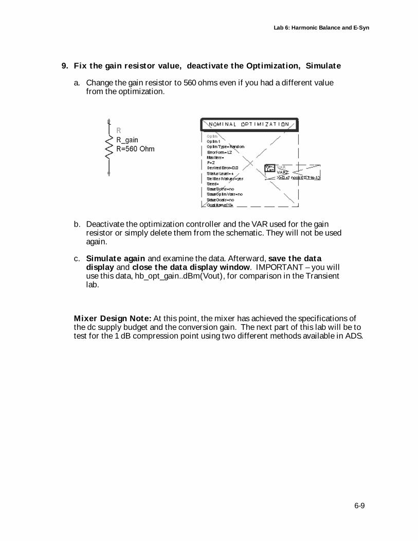
Lab 6: Harmonic Balance and E-Syn
6-9
9. Fix the gain resistor value, deactivate the Optimization, Simulate
a. Change the gain resistor to 560 ohms even if you had a different valuefrom the optimization.
b. Deactivate the optimization controller and the VAR used for the gainresistor or simply delete them from the schematic. They will not be usedagain.
c. Simulate again and examine the data. Afterward, save the datadisplay and close the data display window. IMPORTANT – you willuse this data, hb_opt_gain..dBm(Vout), for comparison in the Transientlab.
Mixer Design Note: At this point, the mixer has achieved the specifications ofthe dc supply budget and the conversion gain. The next part of this lab will be totest for the 1 dB compression point using two different methods available in ADS.
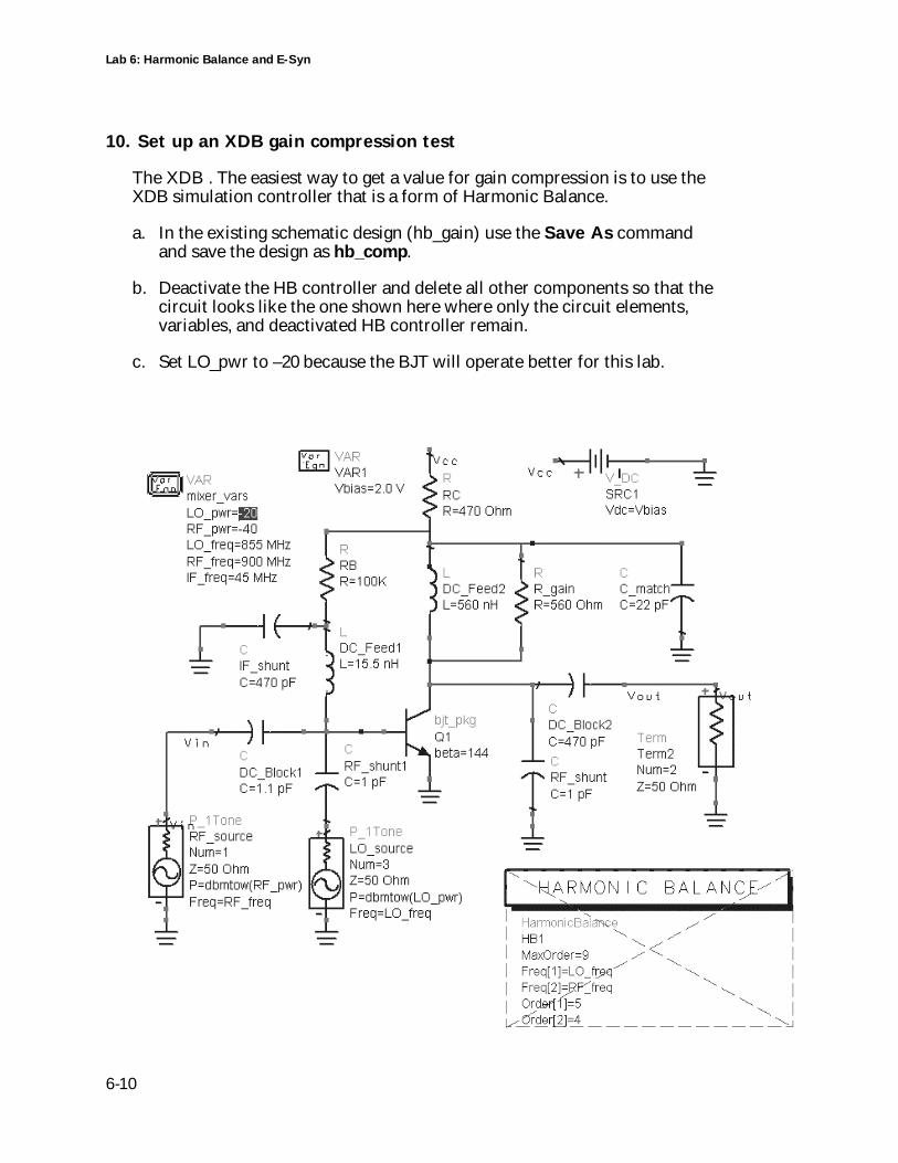
Lab 6: Harmonic Balance and E-Syn
6-10
10. Set up an XDB gain compression test
The XDB . The easiest way to get a value for gain compression is to use theXDB simulation controller that is a form of Harmonic Balance.
a. In the existing schematic design (hb_gain) use the Save As commandand save the design as hb_comp.
b. Deactivate the HB controller and delete all other components so that thecircuit looks like the one shown here where only the circuit elements,variables, and deactivated HB controller remain.
c. Set LO_pwr to –20 because the BJT will operate better for this lab.
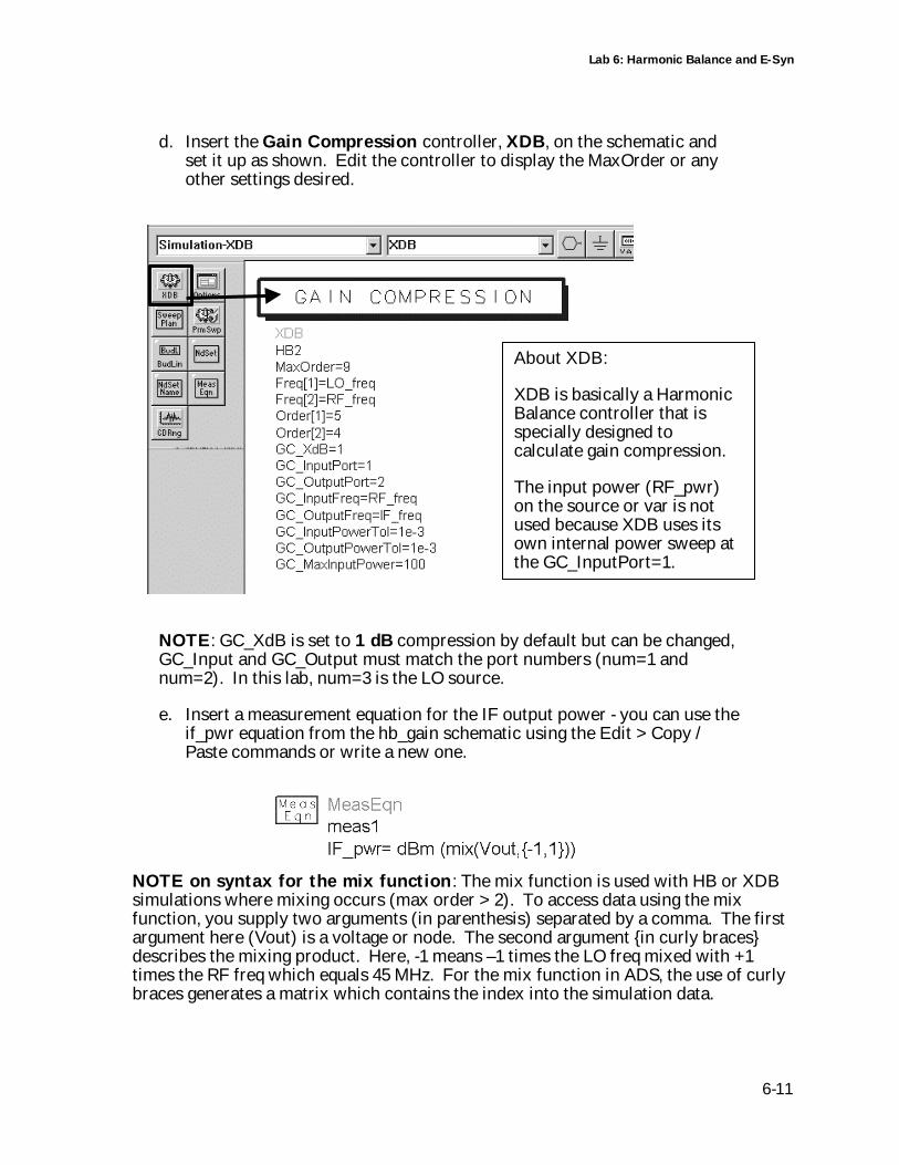
Lab 6: Harmonic Balance and E-Syn
6-11
d. Insert the Gain Compression controller, XDB, on the schematic andset it up as shown. Edit the controller to display the MaxOrder or anyother settings desired.
NOTE: GC_XdB is set to 1 dB compression by default but can be changed,GC_Input and GC_Output must match the port numbers (num=1 andnum=2). In this lab, num=3 is the LO source.
e. Insert a measurement equation for the IF output power - you can use theif_pwr equation from the hb_gain schematic using the Edit > Copy /Paste commands or write a new one.
NOTE on syntax for the mix function: The mix function is used with HB or XDBsimulations where mixing occurs (max order > 2). To access data using the mixfunction, you supply two arguments (in parenthesis) separated by a comma. The firstargument here (Vout) is a voltage or node. The second argument {in curly braces}describes the mixing product. Here, -1 means –1 times the LO freq mixed with +1times the RF freq which equals 45 MHz. For the mix function in ADS, the use of curlybraces generates a matrix which contains the index into the simulation data.
About XDB:
XDB is basically a HarmonicBalance controller that isspecially designed tocalculate gain compression.
The input power (RF_pwr)on the source or var is notused because XDB uses itsown internal power sweep atthe GC_InputPort=1.
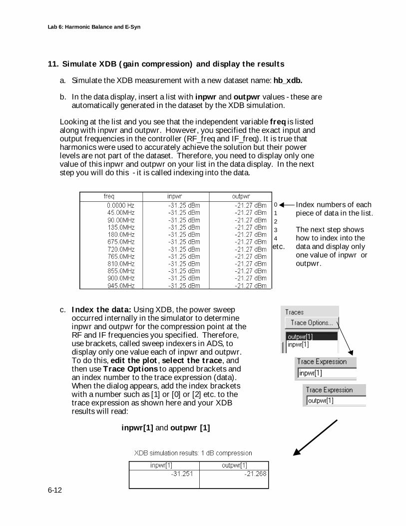
Lab 6: Harmonic Balance and E-Syn
6-12
11. Simulate XDB (gain compression) and display the results
a. Simulate the XDB measurement with a new dataset name: hb_xdb.
b. In the data display, insert a list with inpwr and outpwr values - these areautomatically generated in the dataset by the XDB simulation.
Looking at the list and you see that the independent variable freq is listedalong with inpwr and outpwr. However, you specified the exact input andoutput frequencies in the controller (RF_freq and IF_freq). It is true thatharmonics were used to accurately achieve the solution but their powerlevels are not part of the dataset. Therefore, you need to display only onevalue of this inpwr and outpwr on your list in the data display. In the nextstep you will do this - it is called indexing into the data.
c. Index the data: Using XDB, the power sweepoccurred internally in the simulator to determineinpwr and outpwr for the compression point at theRF and IF frequencies you specified. Therefore,use brackets, called sweep indexers in ADS, todisplay only one value each of inpwr and outpwr.To do this, edit the plot, select the trace, andthen use Trace Options to append brackets andan index number to the trace expression (data).When the dialog appears, add the index bracketswith a number such as [1] or [0] or [2] etc. to thetrace expression as shown here and your XDBresults will read:
inpwr[1] and outpwr [1]
Index numbers of eachpiece of data in the list.
The next step showshow to index into thedata and display onlyone value of inpwr oroutpwr.
0
1
2
3
4
5etc.
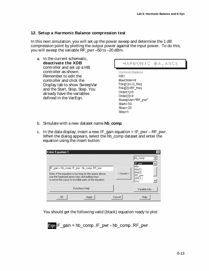
Lab 6: Harmonic Balance and E-Syn
6-13
12. Setup a Harmonic Balance compression test
In this next simulation, you will set up the power sweep and determine the 1 dBcompression point by plotting the output power against the input power. To do this,you will sweep the variable RF_pwr –50 to –20 dBm.
a. In the current schematic,deactivate the XDBcontroller and set up a HBcontroller as shown.Remember to edit thecontroller and click theDisplay tab to show SweepVarand the Start, Stop, Step. Youalready have the variablesdefined in the VarEqn.
b. Simulate with a new dataset name hb_comp.
c. In the data display, insert a new IF_gain equation = IF_pwr – RF_pwr.When the dialog appears, select the hb_comp dataset and enter theequation using the insert button:
You should get the following valid (black) equation ready to plot:
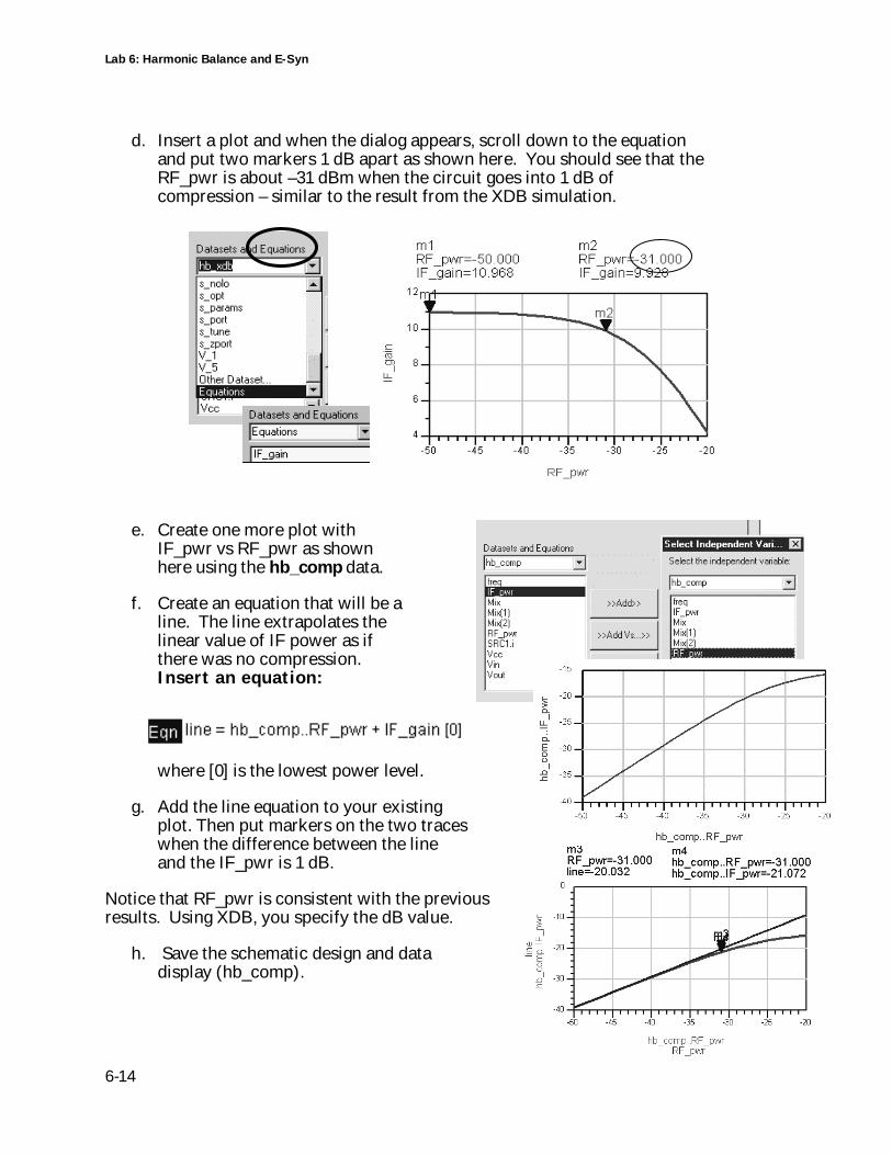
Lab 6: Harmonic Balance and E-Syn
6-14
d. Insert a plot and when the dialog appears, scroll down to the equationand put two markers 1 dB apart as shown here. You should see that theRF_pwr is about –31 dBm when the circuit goes into 1 dB ofcompression – similar to the result from the XDB simulation.
e. Create one more plot withIF_pwr vs RF_pwr as shownhere using the hb_comp data.
f. Create an equation that will be aline. The line extrapolates thelinear value of IF power as ifthere was no compression.Insert an equation:
where [0] is the lowest power level.
g. Add the line equation to your existingplot. Then put markers on the two traceswhen the difference between the lineand the IF_pwr is 1 dB.
Notice that RF_pwr is consistent with the previousresults. Using XDB, you specify the dB value.
h. Save the schematic design and datadisplay (hb_comp).
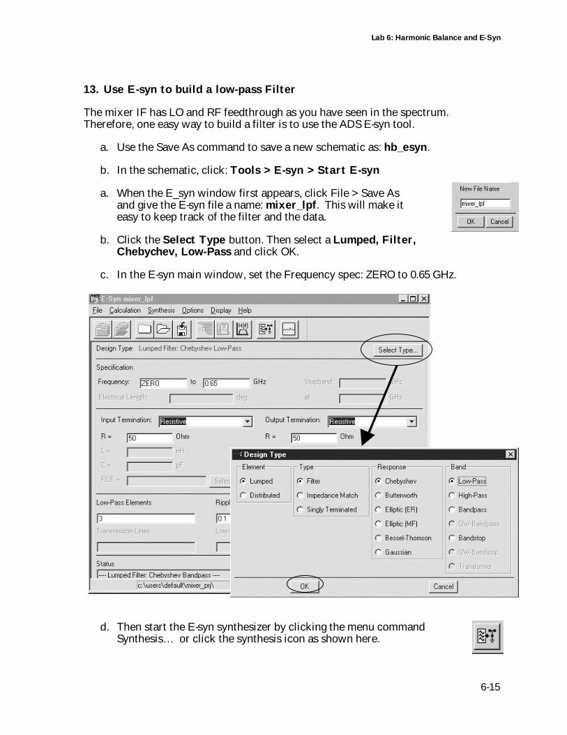
Lab 6: Harmonic Balance and E-Syn
6-15
13. Use E-syn to build a low-pass Filter
The mixer IF has LO and RF feedthrough as you have seen in the spectrum.Therefore, one easy way to build a filter is to use the ADS E-syn tool.
a. Use the Save As command to save a new schematic as: hb_esyn.
b. In the schematic, click: Tools > E-syn > Start E-syn
a. When the E_syn window first appears, click File > Save Asand give the E-syn file a name: mixer_lpf. This will make iteasy to keep track of the filter and the data.
b. Click the Select Type button. Then select a Lumped, Filter,Chebychev, Low-Pass and click OK.
c. In the E-syn main window, set the Frequency spec: ZERO to 0.65 GHz.
d. Then start the E-syn synthesizer by clicking the menu commandSynthesis… or click the synthesis icon as shown here.
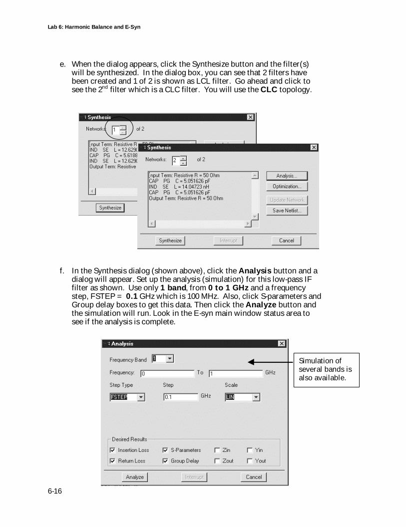
Lab 6: Harmonic Balance and E-Syn
6-16
e. When the dialog appears, click the Synthesize button and the filter(s)will be synthesized. In the dialog box, you can see that 2 filters havebeen created and 1 of 2 is shown as LCL filter. Go ahead and click tosee the 2nd filter which is a CLC filter. You will use the CLC topology.
f. In the Synthesis dialog (shown above), click the Analysis button and adialog will appear. Set up the analysis (simulation) for this low-pass IFfilter as shown. Use only 1 band, from 0 to 1 GHz and a frequencystep, FSTEP = 0.1 GHz which is 100 MHz. Also, click S-parameters andGroup delay boxes to get this data. Then click the Analyze button andthe simulation will run. Look in the E-syn main window status area tosee if the analysis is complete.
Simulation ofseveral bands isalso available.
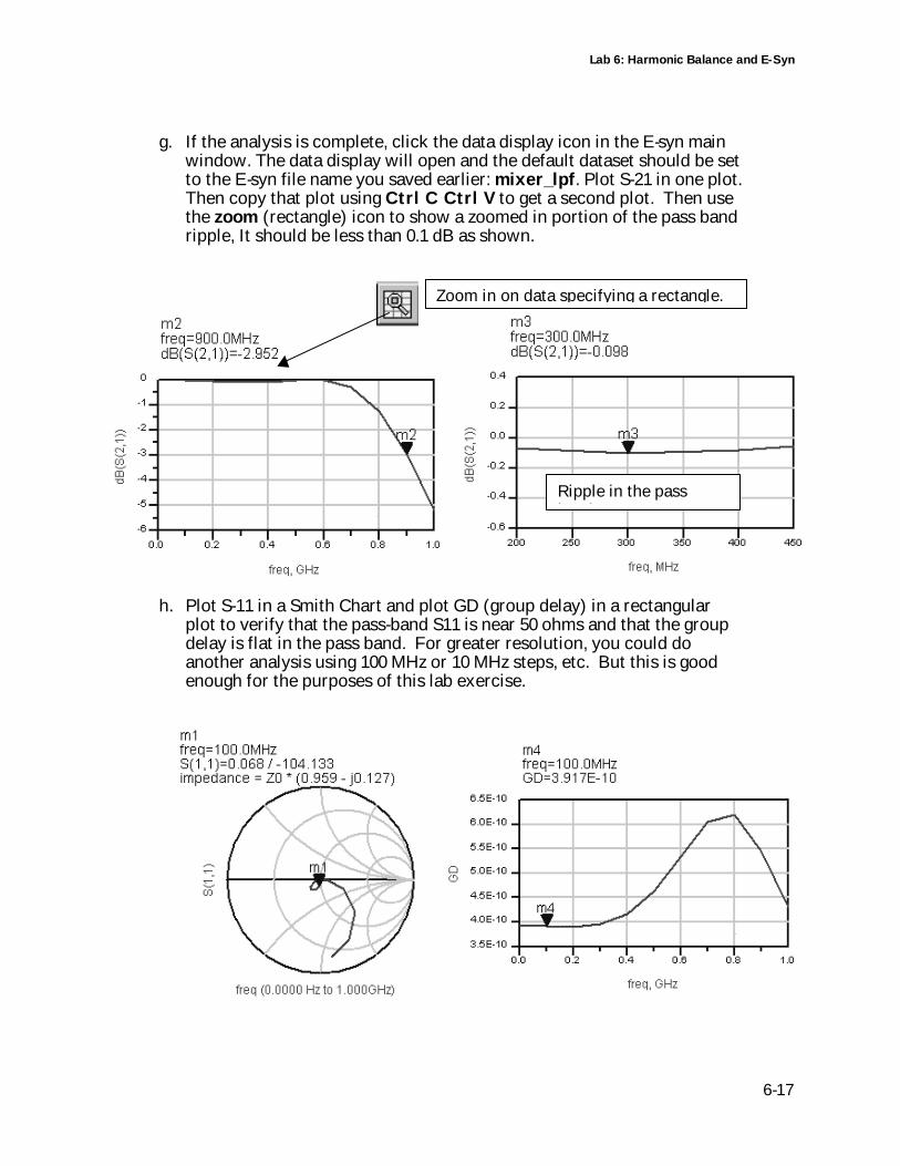
Lab 6: Harmonic Balance and E-Syn
6-17
g. If the analysis is complete, click the data display icon in the E-syn mainwindow. The data display will open and the default dataset should be setto the E-syn file name you saved earlier: mixer_lpf. Plot S-21 in one plot.Then copy that plot using Ctrl C Ctrl V to get a second plot. Then usethe zoom (rectangle) icon to show a zoomed in portion of the pass bandripple, It should be less than 0.1 dB as shown.
h. Plot S-11 in a Smith Chart and plot GD (group delay) in a rectangularplot to verify that the pass-band S11 is near 50 ohms and that the groupdelay is flat in the pass band. For greater resolution, you could doanother analysis using 100 MHz or 10 MHz steps, etc. But this is goodenough for the purposes of this lab exercise.
Zoom in on data specifying a rectangle.
Ripple in the passband.
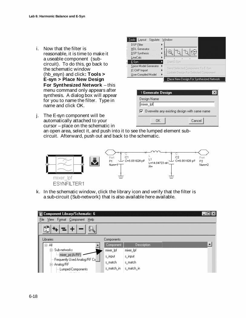
Lab 6: Harmonic Balance and E-Syn
6-18
i. Now that the filter isreasonable, it is time to make ita useable component (sub-circuit). To do this, go back tothe schematic window(hb_esyn) and click: Tools >E-syn > Place New DesignFor Synthesized Network – thismenu command only appears aftersynthesis. A dialog box will appearfor you to name the filter. Type inname and click OK.
j. The E-syn component will beautomatically attached to yourcursor – place on the schematic inan open area, select it, and push into it to see the lumped element sub-circuit. Afterward, push out and back to the schematic.
k. In the schematic window, click the library icon and verify that the filter isa sub-circuit (Sub-network) that is also available here available.
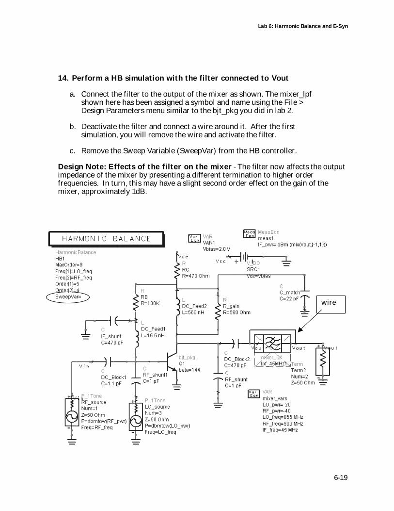
Lab 6: Harmonic Balance and E-Syn
6-19
14. Perform a HB simulation with the filter connected to Vout
a. Connect the filter to the output of the mixer as shown. The mixer_lpfshown here has been assigned a symbol and name using the File >Design Parameters menu similar to the bjt_pkg you did in lab 2.
b. Deactivate the filter and connect a wire around it. After the firstsimulation, you will remove the wire and activate the filter.
c. Remove the Sweep Variable (SweepVar) from the HB controller.
Design Note: Effects of the filter on the mixer - The filter now affects the outputimpedance of the mixer by presenting a different termination to higher orderfrequencies. In turn, this may have a slight second order effect on the gain of themixer, approximately 1dB.
wire
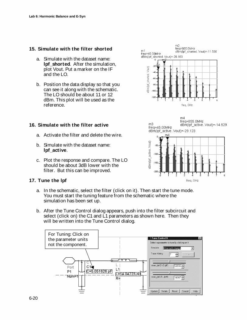
Lab 6: Harmonic Balance and E-Syn
6-20
15. Simulate with the filter shorted
a. Simulate with the dataset name:lpf_shorted. After the simulation,plot Vout. Put a marker on the IFand the LO.
b. Position the data display so that youcan see it along with the schematic.The LO should be about 11 or 12dBm. This plot will be used as thereference.
16. Simulate with the filter active
a. Activate the filter and delete the wire.
b. Simulate with the dataset name:lpf_active.
c. Plot the response and compare. The LOshould be about 3dB lower with thefilter. But this can be improved.
17. Tune the lpf
a. In the schematic, select the filter (click on it). Then start the tune mode.You must start the tuning feature from the schematic where thesimulation has been set up.
b. After the Tune Control dialog appears, push into the filter subcircuit andselect (click on) the C1 and L1 parameters as shown here. Then theywill be written into the Tune Control dialog.
For Tuning: Click onthe parameter unitsnot the component.
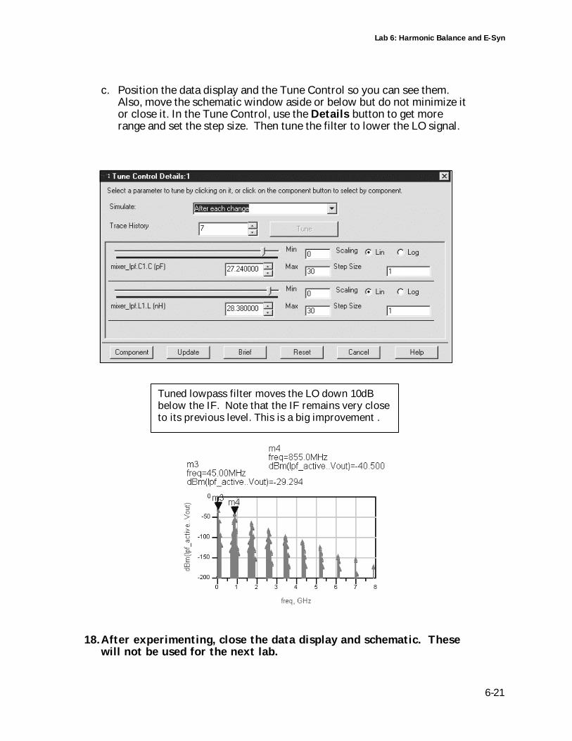
Lab 6: Harmonic Balance and E-Syn
6-21
c. Position the data display and the Tune Control so you can see them.Also, move the schematic window aside or below but do not minimize itor close it. In the Tune Control, use the Details button to get morerange and set the step size. Then tune the filter to lower the LO signal.
18. After experimenting, close the data display and schematic. Thesewill not be used for the next lab.
Tuned lowpass filter moves the LO down 10dBbelow the IF. Note that the IF remains very closeto its previous level. This is a big improvement .
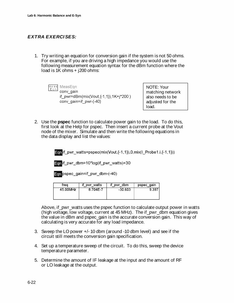
Lab 6: Harmonic Balance and E-Syn
6-22
EXTRA EXERCISES:
1. Try writing an equation for conversion gain if the system is not 50 ohms.For example, if you are driving a high impedance you would use thefollowing measurement equation syntax for the dBm function where theload is 1K ohms + j200 ohms:
2. Use the pspec function to calculate power gain to the load. To do this,first look at the Help for pspec. Then insert a current probe at the Voutnode of the mixer. Simulate and then write the following equations inthe data display and list the values:
Above, if_pwr_watts uses the pspec function to calculate output power in watts(high voltage, low voltage, current at 45 MHz). The if_pwr_dbm equation givesthe value in dBm and pspec_gain is the accurate conversion gain. This way ofcalculating is very accurate for any load impedance.
3. Sweep the LO power +/- 10 dbm (around -10 dbm level) and see if thecircuit still meets the conversion gain specification.
4. Set up a temperature sweep of the circuit. To do this, sweep the devicetemperature parameter.
5. Determine the amount of IF leakage at the input and the amount of RFor LO leakage at the output.
NOTE: Yourmatching networkalso needs to beadjusted for theload.
7
This chapter shows how to use Harmonic Balance for two-tonemeasurements such as TOI, NF, and others.
Lab 7: Advanced Harmonic Balance
Mixer Simulations
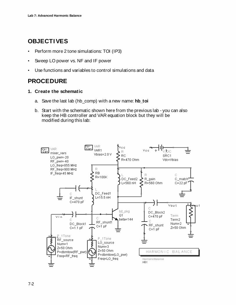
Lab 7: Advanced Harmonic Balance
7-2
OBJECTIVES
• Perform more 2 tone simulations: TOI (IP3)
• Sweep LO power vs. NF and IF power
• Use functions and variables to control simulations and data
PROCEDURE
1. Create the schematic
a. Save the last lab (hb_comp) with a new name: hb_toi
b. Start with the schematic shown here from the previous lab - you can alsokeep the HB controller and VAR equation block but they will bemodified during this lab:
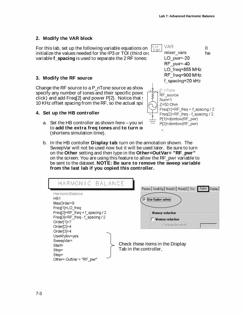
Lab 7: Advanced Harmonic Balance
7-3
2. Modify the VAR block
For this lab, set up the following variable equations on the schematic. This VAR willinitialize the values needed for the IP3 or TOI (third order intercept) simulation. Thevariable f_spacing is used to separate the 2 RF tones:
3. Modify the RF source
Change the RF source to a P_nTone source as shown. This source allows you tospecify any number of tones and their specific power levels. Edit the source (doubleclick) and add Freq[2] and power P[2}. Notice that you use the f_spacing / 2 to give10 KHz offset spacing from the RF, so the actual spacing is 20 KHz.
4. Set up the HB controller
a. Set the HB controller as shown here – you will have to edit the controllerto add the extra freq tones and to turn on the Krylov solver(shortens simulation time).
b. In the HB contoller Display tab: turn on the annotation shown. TheSweepVar will not be used now but it will be used later. Be sure to turnon the Other setting and then type in the Other=OutVar= ”RF_pwr”on the screen. You are using this feature to allow the RF_pwr variable tobe sent to the dataset. NOTE: Be sure to remove the sweep variablefrom the last lab if you copied this controller.
Check these items in the DisplayTab in the controller,
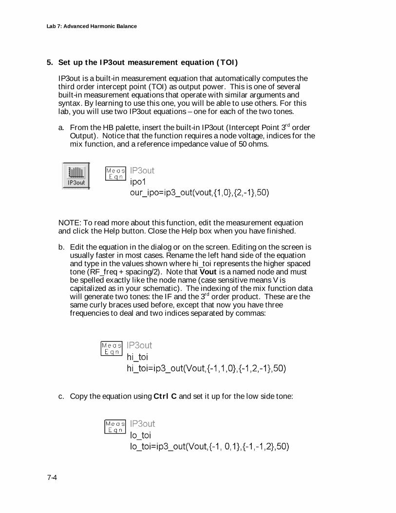
Lab 7: Advanced Harmonic Balance
7-4
5. Set up the IP3out measurement equation (TOI)
IP3out is a built-in measurement equation that automatically computes thethird order intercept point (TOI) as output power. This is one of severalbuilt-in measurement equations that operate with similar arguments andsyntax. By learning to use this one, you will be able to use others. For thislab, you will use two IP3out equations – one for each of the two tones.
a. From the HB palette, insert the built-in IP3out (Intercept Point 3rd orderOutput). Notice that the function requires a node voltage, indices for themix function, and a reference impedance value of 50 ohms.
NOTE: To read more about this function, edit the measurement equationand click the Help button. Close the Help box when you have finished.
b. Edit the equation in the dialog or on the screen. Editing on the screen isusually faster in most cases. Rename the left hand side of the equationand type in the values shown where hi_toi represents the higher spacedtone (RF_freq + spacing/2). Note that Vout is a named node and mustbe spelled exactly like the node name (case sensitive means V iscapitalized as in your schematic). The indexing of the mix function datawill generate two tones: the IF and the 3rd order product. These are thesame curly braces used before, except that now you have threefrequencies to deal and two indices separated by commas:
c. Copy the equation using Ctrl C and set it up for the low side tone:
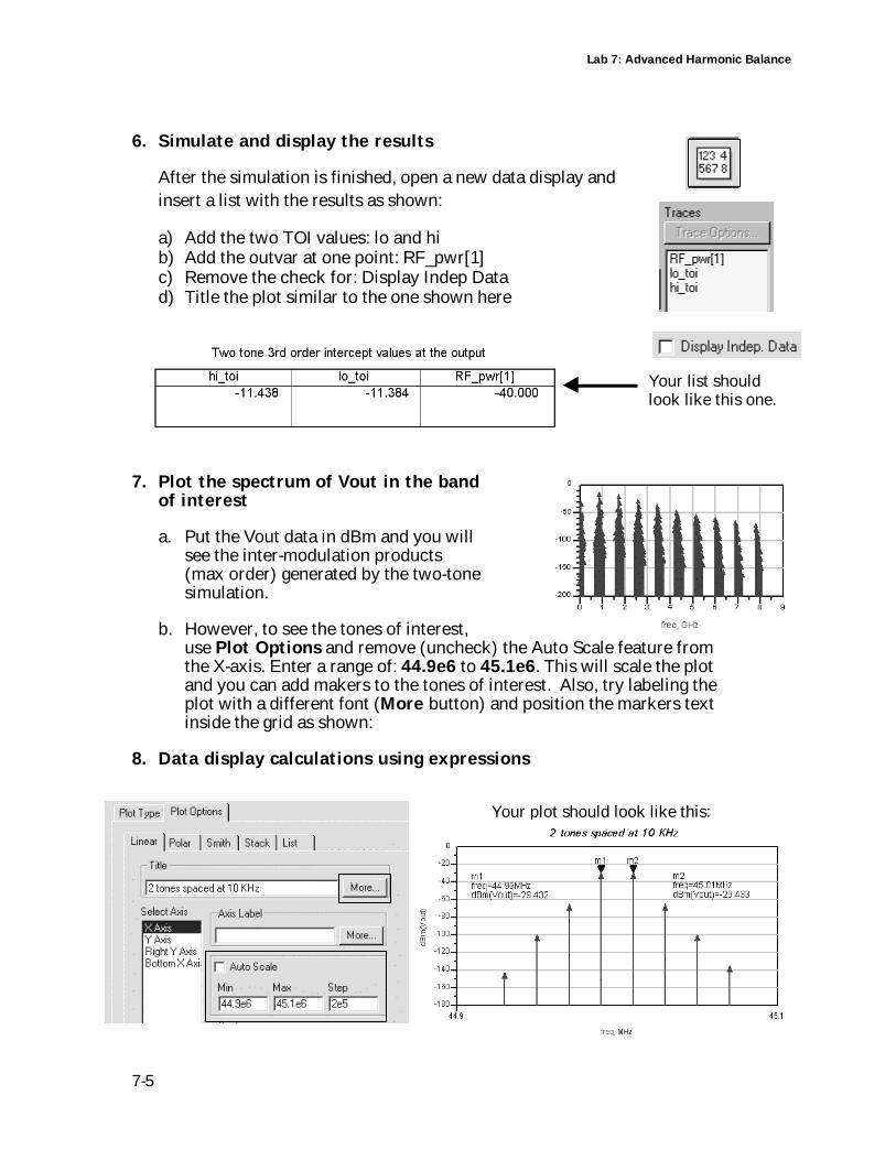
Lab 7: Advanced Harmonic Balance
7-5
6. Simulate and display the results
After the simulation is finished, open a new data display andinsert a list with the results as shown:
a) Add the two TOI values: lo and hib) Add the outvar at one point: RF_pwr[1]c) Remove the check for: Display Indep Datad) Title the plot similar to the one shown here
7. Plot the spectrum of Vout in the bandof interest
a. Put the Vout data in dBm and you willsee the inter-modulation products(max order) generated by the two-tonesimulation.
b. However, to see the tones of interest,use Plot Options and remove (uncheck) the Auto Scale feature fromthe X-axis. Enter a range of: 44.9e6 to 45.1e6. This will scale the plotand you can add makers to the tones of interest. Also, try labeling theplot with a different font (More button) and position the markers textinside the grid as shown:
8. Data display calculations using expressions
Your list shouldlook like this one.
Your plot should look like this:
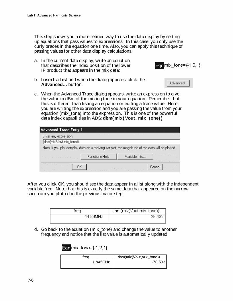
Lab 7: Advanced Harmonic Balance
7-6
This step shows you a more refined way to use the data display by settingup equations that pass values to expressions. In this case, you only use thecurly braces in the equation one time. Also, you can apply this technique ofpassing values for other data display calculations.
a. In the current data display, write an equationthat describes the index position of the lowerIF product that appears in the mix data:
b. Insert a list and when the dialog appears, click theAdvanced… button.
c. When the Advanced Trace dialog appears, write an expression to givethe value in dBm of the mixing tone in your equation. Remember thatthis is different than listing an equation or editing a trace value. Here,you are writing the expression and you are passing the value from yourequation (mix_tone) into the expression. This is one of the powerfuldata index capabilities in ADS: dbm(mix(Vout, mix_tone)).
After you click OK, you should see the data appear in a list along with the independentvariable freq. Note that this is exactly the same data that appeared on the narrowspectrum you plotted in the previous major step.
d. Go back to the equation (mix_tone) and change the value to anotherfrequency and notice that the list value is automatically updated.
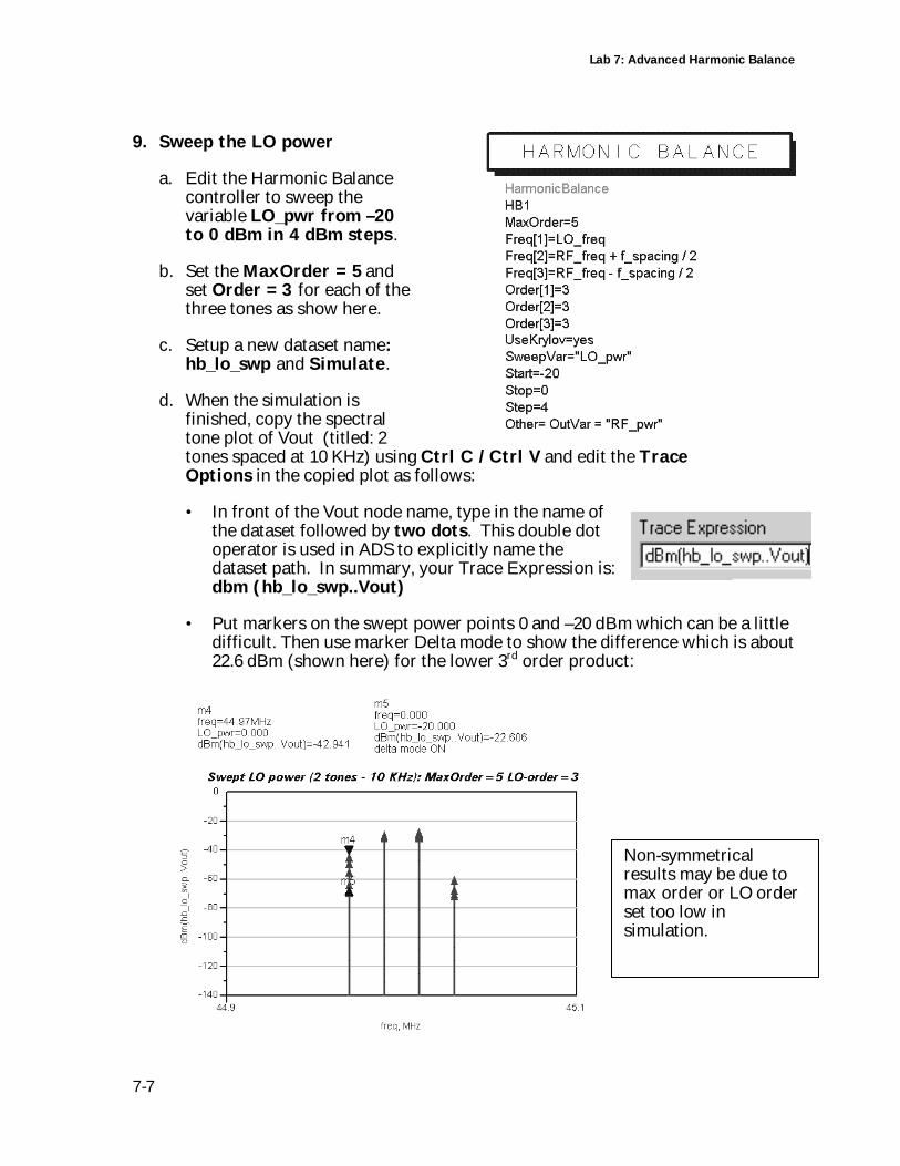
Lab 7: Advanced Harmonic Balance
7-7
9. Sweep the LO power
a. Edit the Harmonic Balancecontroller to sweep thevariable LO_pwr from –20to 0 dBm in 4 dBm steps.
b. Set the MaxOrder = 5 andset Order = 3 for each of thethree tones as show here.
c. Setup a new dataset name:hb_lo_swp and Simulate.
d. When the simulation isfinished, copy the spectraltone plot of Vout (titled: 2tones spaced at 10 KHz) using Ctrl C / Ctrl V and edit the TraceOptions in the copied plot as follows:
• In front of the Vout node name, type in the name ofthe dataset followed by two dots. This double dotoperator is used in ADS to explicitly name thedataset path. In summary, your Trace Expression is:dbm (hb_lo_swp..Vout)
• Put markers on the swept power points 0 and –20 dBm which can be a littledifficult. Then use marker Delta mode to show the difference which is about22.6 dBm (shown here) for the lower 3rd order product:
Non-symmetricalresults may be due tomax order or LO orderset too low insimulation.
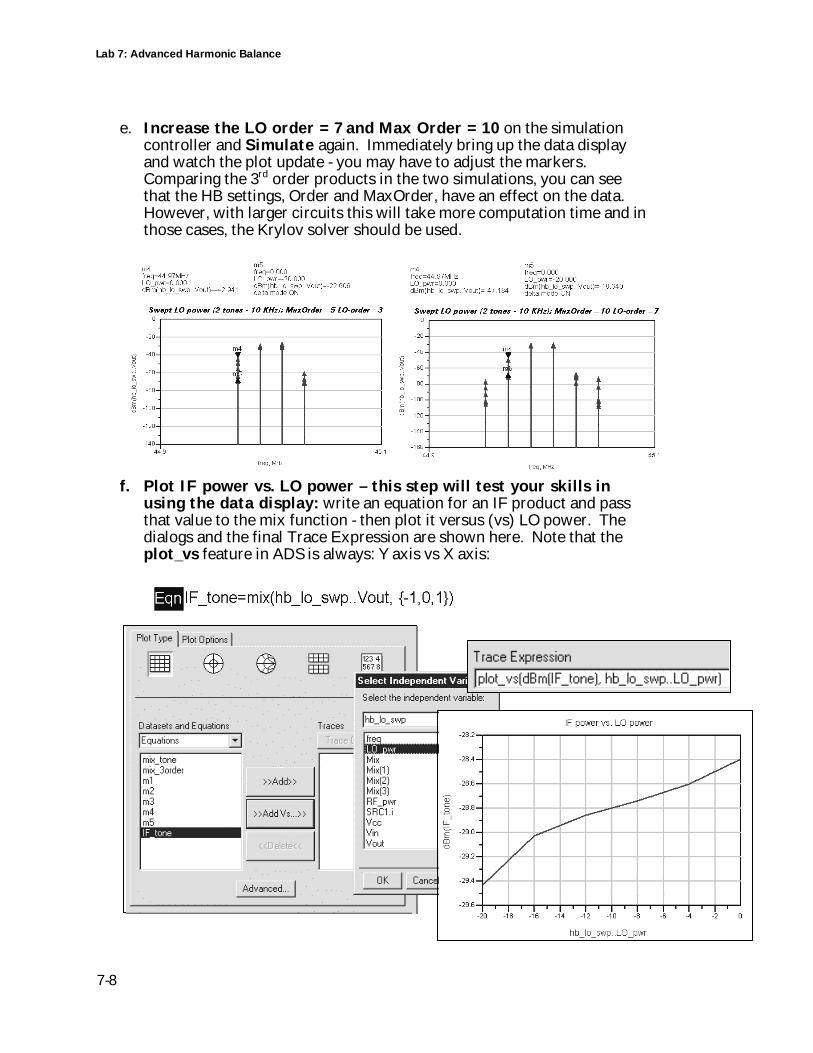
Lab 7: Advanced Harmonic Balance
7-8
e. Increase the LO order = 7 and Max Order = 10 on the simulationcontroller and Simulate again. Immediately bring up the data displayand watch the plot update - you may have to adjust the markers.Comparing the 3rd order products in the two simulations, you can seethat the HB settings, Order and MaxOrder, have an effect on the data.However, with larger circuits this will take more computation time and inthose cases, the Krylov solver should be used.
f. Plot IF power vs. LO power – this step will test your skills inusing the data display: write an equation for an IF product and passthat value to the mix function - then plot it versus (vs) LO power. Thedialogs and the final Trace Expression are shown here. Note that theplot_vs feature in ADS is always: Y axis vs X axis:
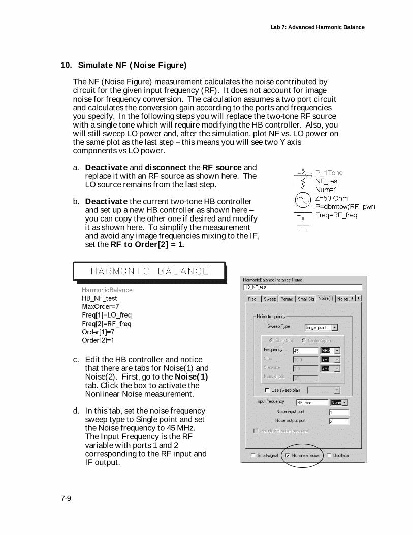
Lab 7: Advanced Harmonic Balance
7-9
10. Simulate NF (Noise Figure)
The NF (Noise Figure) measurement calculates the noise contributed bycircuit for the given input frequency (RF). It does not account for imagenoise for frequency conversion. The calculation assumes a two port circuitand calculates the conversion gain according to the ports and frequenciesyou specify. In the following steps you will replace the two-tone RF sourcewith a single tone which will require modifying the HB controller. Also, youwill still sweep LO power and, after the simulation, plot NF vs. LO power onthe same plot as the last step – this means you will see two Y axiscomponents vs LO power.
a. Deactivate and disconnect the RF source andreplace it with an RF source as shown here. TheLO source remains from the last step.
b. Deactivate the current two-tone HB controllerand set up a new HB controller as shown here –you can copy the other one if desired and modifyit as shown here. To simplify the measurementand avoid any image frequencies mixing to the IF,set the RF to Order[2] = 1.
c. Edit the HB controller and noticethat there are tabs for Noise(1) andNoise(2). First, go to the Noise(1)tab. Click the box to activate theNonlinear Noise measurement.
d. In this tab, set the noise frequencysweep type to Single point and setthe Noise frequency to 45 MHz.The Input Frequency is the RFvariable with ports 1 and 2corresponding to the RF input andIF output.
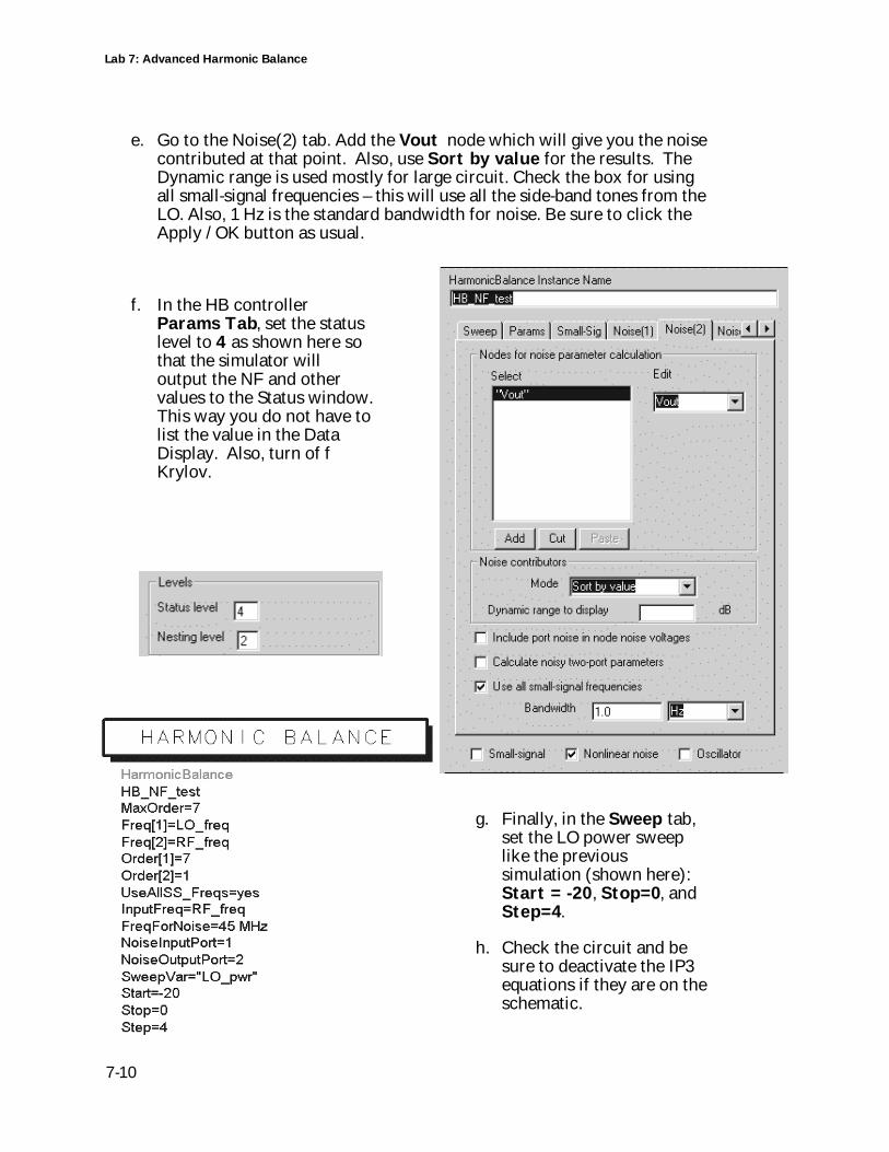
Lab 7: Advanced Harmonic Balance
7-10
e. Go to the Noise(2) tab. Add the Vout node which will give you the noisecontributed at that point. Also, use Sort by value for the results. TheDynamic range is used mostly for large circuit. Check the box for usingall small-signal frequencies – this will use all the side-band tones from theLO. Also, 1 Hz is the standard bandwidth for noise. Be sure to click theApply / OK button as usual.
f. In the HB controllerParams Tab, set the statuslevel to 4 as shown here sothat the simulator willoutput the NF and othervalues to the Status window.This way you do not have tolist the value in the DataDisplay. Also, turn of fKrylov.
g. Finally, in the Sweep tab,set the LO power sweeplike the previoussimulation (shown here):Start = -20, Stop=0, andStep=4.
h. Check the circuit and besure to deactivate the IP3equations if they are on theschematic.
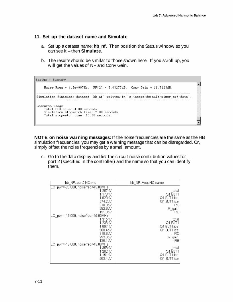
Lab 7: Advanced Harmonic Balance
7-11
11. Set up the dataset name and Simulate
a. Set up a dataset name: hb_nf. Then position the Status window so youcan see it – then Simulate.
b. The results should be similar to those shown here. If you scroll up, youwill get the values of NF and Conv Gain.
NOTE on noise warning messages: If the noise frequencies are the same as the HBsimulation frequencies, you may get a warning message that can be disregarded. Or,simply offset the noise frequencies by a small amount.
c. Go to the data display and list the circuit noise contribution values forport 2 (specified in the controller) and the name so that you can identifythem.
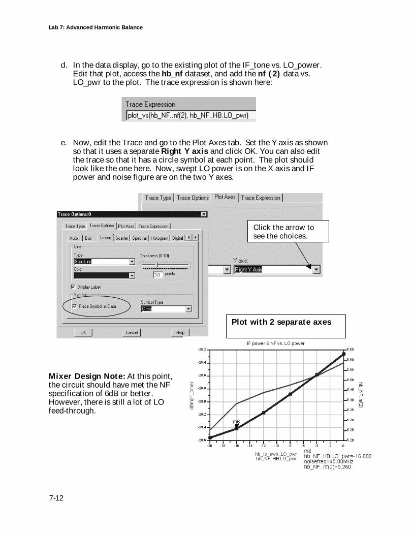
Lab 7: Advanced Harmonic Balance
7-12
d. In the data display, go to the existing plot of the IF_tone vs. LO_power.Edit that plot, access the hb_nf dataset, and add the nf (2) data vs.LO_pwr to the plot. The trace expression is shown here:
e. Now, edit the Trace and go to the Plot Axes tab. Set the Y axis as shownso that it uses a separate Right Y axis and click OK. You can also editthe trace so that it has a circle symbol at each point. The plot shouldlook like the one here. Now, swept LO power is on the X axis and IFpower and noise figure are on the two Y axes.
Mixer Design Note: At this point,the circuit should have met the NFspecification of 6dB or better.However, there is still a lot of LOfeed-through.
Click the arrow tosee the choices.
Plot with 2 separate axes
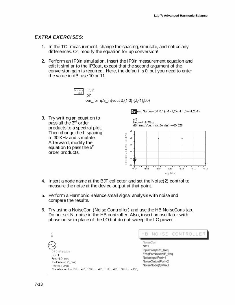
Lab 7: Advanced Harmonic Balance
7-13
EXTRA EXERCISES:
1. In the TOI measurement, change the spacing, simulate, and notice anydifferences. Or, modify the equation for up conversion!
2. Perform an IP3in simulation. Insert the IP3in measurement equation andedit it similar to the IP3out, except that the second argument of theconversion gain is required. Here, the default is 0, but you need to enterthe value in dB: use 10 or 11.
3. Try writing an equation topass all the 3rd orderproducts to a spectral plot.Then change the f_spacingto 30 KHz and simulate.Afterward, modify theequation to pass the 5th
order products.
4. Insert a node name at the BJT collector and set the Noise(2) control tomeasure the noise at the device output at that point.
5. Perform a Harmonic Balance small signal analysis with noise andcompare the results.
6. Try using a NoiseCon (Noise Controller) and use the HB NoiseCons tab.Do not set NLnoise in the HB controller. Also, insert an oscillator withphase noise in place of the LO but do not sweep the LO power.

Lab 7: Advanced Harmonic Balance
7-14
THIS PAGE IS INTENTIONALLY BLANK.
8
This chapter shows how to use the Transient simulator tomeasure the mixer in the time domain.
Lab 8: Transient Simulation
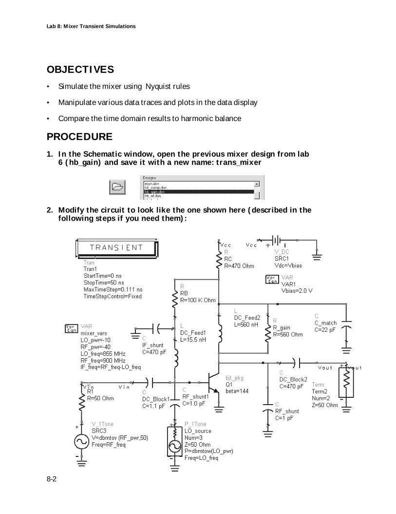
Lab 8: Mixer Transient Simulations
8-2
OBJECTIVES
• Simulate the mixer using Nyquist rules
• Manipulate various data traces and plots in the data display
• Compare the time domain results to harmonic balance
PROCEDURE
1. In the Schematic window, open the previous mixer design from lab6 (hb_gain) and save it with a new name: trans_mixer
2. Modify the circuit to look like the one shown here (described in thefollowing steps if you need them):
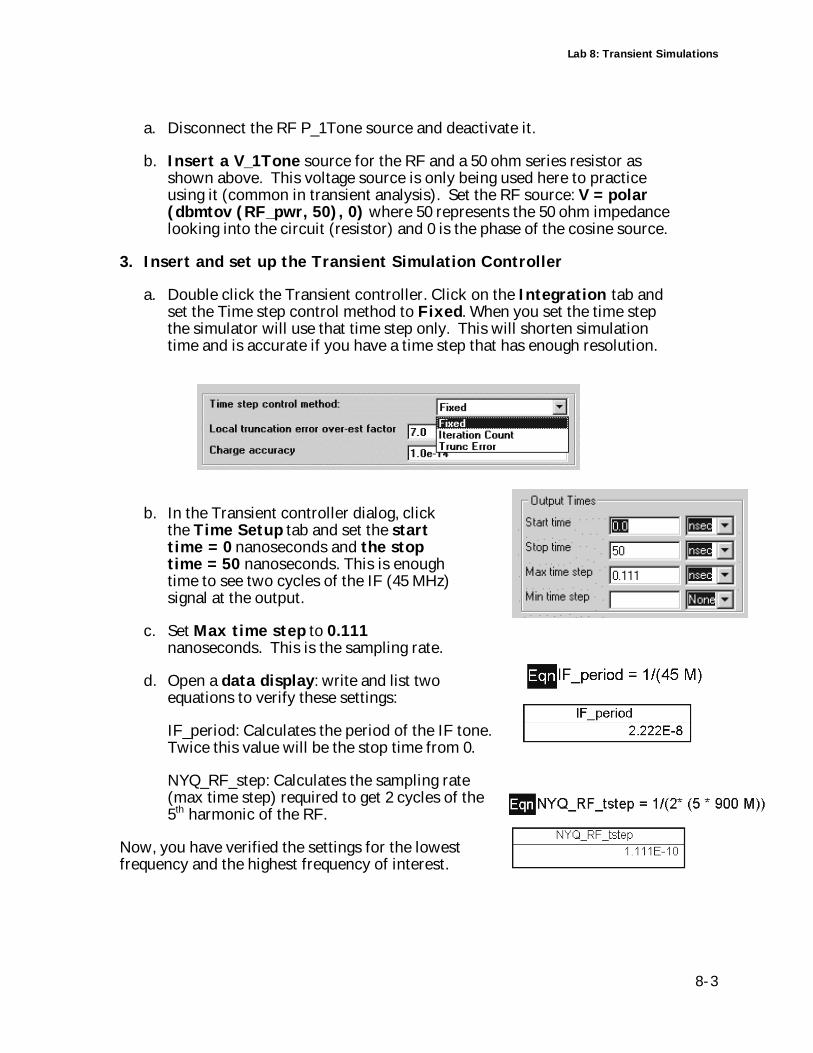
Lab 8: Transient Simulations
38-
a. Disconnect the RF P_1Tone source and deactivate it.
b. Insert a V_1Tone source for the RF and a 50 ohm series resistor asshown above. This voltage source is only being used here to practiceusing it (common in transient analysis). Set the RF source: V = polar(dbmtov (RF_pwr, 50), 0) where 50 represents the 50 ohm impedancelooking into the circuit (resistor) and 0 is the phase of the cosine source.
3. Insert and set up the Transient Simulation Controller
a. Double click the Transient controller. Click on the Integration tab andset the Time step control method to Fixed. When you set the time stepthe simulator will use that time step only. This will shorten simulationtime and is accurate if you have a time step that has enough resolution.
b. In the Transient controller dialog, clickthe Time Setup tab and set the starttime = 0 nanoseconds and the stoptime = 50 nanoseconds. This is enoughtime to see two cycles of the IF (45 MHz)signal at the output.
c. Set Max time step to 0.111nanoseconds. This is the sampling rate.
d. Open a data display: write and list twoequations to verify these settings:
IF_period: Calculates the period of the IF tone.Twice this value will be the stop time from 0.
NYQ_RF_step: Calculates the sampling rate(max time step) required to get 2 cycles of the5th harmonic of the RF.
Now, you have verified the settings for the lowestfrequency and the highest frequency of interest.
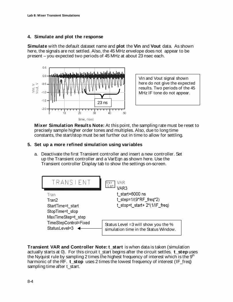
Lab 8: Mixer Transient Simulations
8-4
4. Simulate and plot the response
Simulate with the default dataset name and plot the Vin and Vout data. As shownhere, the signals are not settled. Also, the 45 MHz envelope does not appear to bepresent – you expected two periods of 45 MHz at about 23 nsec each.
Mixer Simulation Results Note: At this point, the sampling rate must be reset toprecisely sample higher order tones and multiples. Also, due to long timeconstants, the start/stop must be set further out in time to allow for settling.
5. Set up a more refined simulation using variables
a. Deactivate the first Transient controller and insert a new controller. Setup the Transient controller and a VarEqn as shown here. Use theTransient controller Display tab to show the settings on-screen.
Transient VAR and Controller Note: t_start is when data is taken (simulationactually starts at 0). For this circuit t_start begins after the circuit settles. t_step usesthe Nyquist rule by sampling 2 times the highest frequency of interest which is the 9th
harmonic of the RF. t_stop uses 2 times the lowest frequency of interest (IF_freq)sampling time after t_start.
Status Level =3 will show you the %simulation time in the Status Window.
Vin and Vout signal shownhere do not give the expectedresults. Two periods of the 45MHz IF tone do not appear.
23 ns
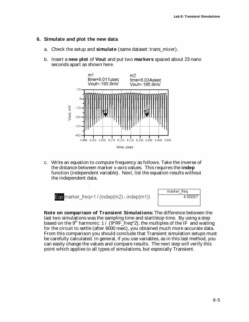
Lab 8: Transient Simulations
58-
6. Simulate and plot the new data
a. Check the setup and simulate (same dataset: trans_mixer).
b. Insert a new plot of Vout and put two markers spaced about 23 nanoseconds apart as shown here.
c. Write an equation to compute frequency as follows. Take the inverse ofthe distance between marker x-axis values. This requires the indepfunction (independent variable). Next, list the equation results withoutthe independent data.
Note on comparison of Transient Simulations: The difference between thelast two simulations was the sampling time and start/stop time. By using a stepbased on the 9th harmonic: 1 / (9*RF_freq*2), the multiples of the IF and waitingfor the circuit to settle (after 6000 nsec), you obtained much more accurate data.From this comparison you should conclude that Transient simulation setups mustbe carefully calculated. In general, if you use variables, as in this last method, youcan easily change the values and compare results. The next step will verify thispoint which applies to all types of simulations, but especially Transient.
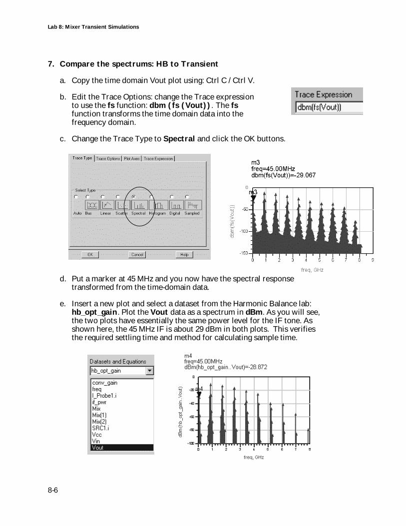
Lab 8: Mixer Transient Simulations
8-6
7. Compare the spectrums: HB to Transient
a. Copy the time domain Vout plot using: Ctrl C / Ctrl V.
b. Edit the Trace Options: change the Trace expressionto use the fs function: dbm (fs (Vout)). The fsfunction transforms the time domain data into thefrequency domain.
c. Change the Trace Type to Spectral and click the OK buttons.
d. Put a marker at 45 MHz and you now have the spectral responsetransformed from the time-domain data.
e. Insert a new plot and select a dataset from the Harmonic Balance lab:hb_opt_gain. Plot the Vout data as a spectrum in dBm. As you will see,the two plots have essentially the same power level for the IF tone. Asshown here, the 45 MHz IF is about 29 dBm in both plots. This verifiesthe required settling time and method for calculating sample time.
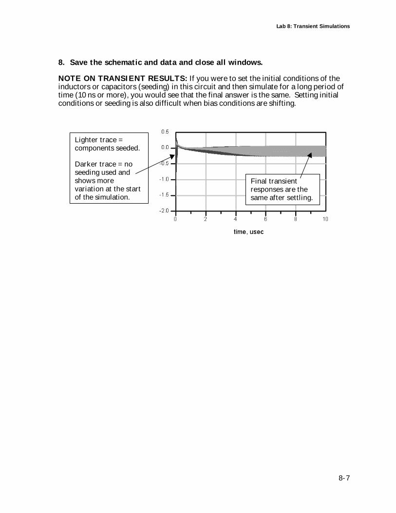
Lab 8: Transient Simulations
78-
8. Save the schematic and data and close all windows.
NOTE ON TRANSIENT RESULTS: If you were to set the initial conditions of theinductors or capacitors (seeding) in this circuit and then simulate for a long period oftime (10 ns or more), you would see that the final answer is the same. Setting initialconditions or seeding is also difficult when bias conditions are shifting.
Lighter trace =components seeded.
Darker trace = noseeding used andshows morevariation at the startof the simulation.
Final transientresponses are thesame after settling.
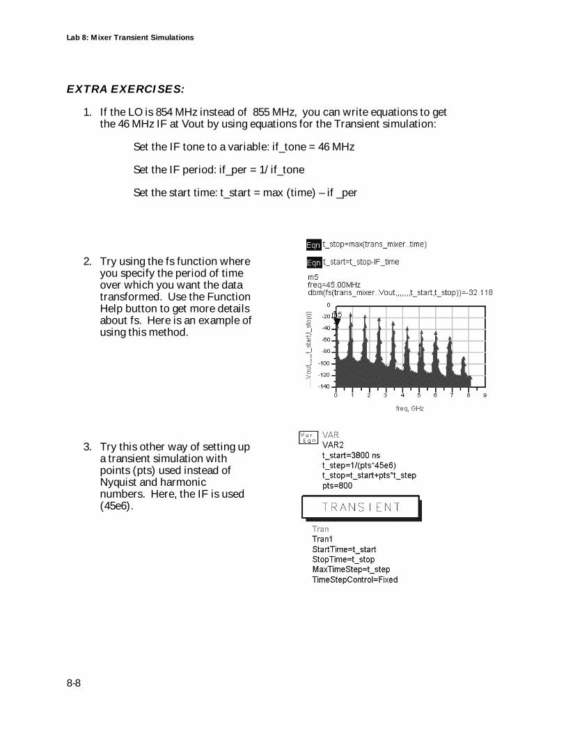
Lab 8: Mixer Transient Simulations
8-8
EXTRA EXERCISES:
1. If the LO is 854 MHz instead of 855 MHz, you can write equations to getthe 46 MHz IF at Vout by using equations for the Transient simulation:
Set the IF tone to a variable: if_tone = 46 MHz
Set the IF period: if_per = 1/ if_tone
Set the start time: t_start = max (time) – if _per
2. Try using the fs function whereyou specify the period of timeover which you want the datatransformed. Use the FunctionHelp button to get more detailsabout fs. Here is an example ofusing this method.
3. Try this other way of setting upa transient simulation withpoints (pts) used instead ofNyquist and harmonicnumbers. Here, the IF is used(45e6).
9
This chapter shows how to use Circuit Envelope to measure timeand frequency of an output signal when the input is a modulatedsource such as GSM, CDMA, etc.
Lab 9: Circuit Envelope Simulations
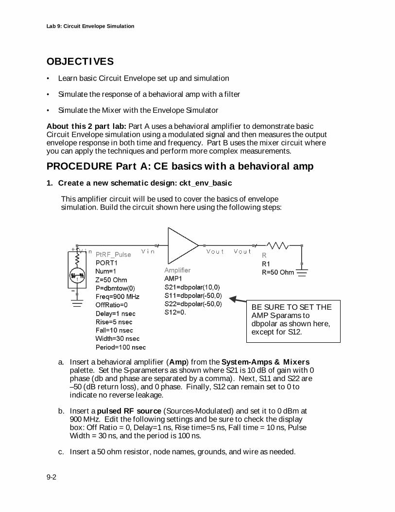
Lab 9: Circuit Envelope Simulation
9-2
OBJECTIVES
• Learn basic Circuit Envelope set up and simulation
• Simulate the response of a behavioral amp with a filter
• Simulate the Mixer with the Envelope Simulator
About this 2 part lab: Part A uses a behavioral amplifier to demonstrate basicCircuit Envelope simulation using a modulated signal and then measures the outputenvelope response in both time and frequency. Part B uses the mixer circuit whereyou can apply the techniques and perform more complex measurements.
PROCEDURE Part A: CE basics with a behavioral amp
1. Create a new schematic design: ckt_env_basic
This amplifier circuit will be used to cover the basics of envelopesimulation. Build the circuit shown here using the following steps:
a. Insert a behavioral amplifier (Amp) from the System-Amps & Mixerspalette. Set the S-parameters as shown where S21 is 10 dB of gain with 0phase (db and phase are separated by a comma). Next, S11 and S22 are–50 (dB return loss), and 0 phase. Finally, S12 can remain set to 0 toindicate no reverse leakage.
b. Insert a pulsed RF source (Sources-Modulated) and set it to 0 dBm at900 MHz. Edit the following settings and be sure to check the displaybox: Off Ratio = 0, Delay=1 ns, Rise time=5 ns, Fall time = 10 ns, PulseWidth = 30 ns, and the period is 100 ns.
c. Insert a 50 ohm resistor, node names, grounds, and wire as needed.
BE SURE TO SET THEAMP S-params todbpolar as shown here,except for S12.
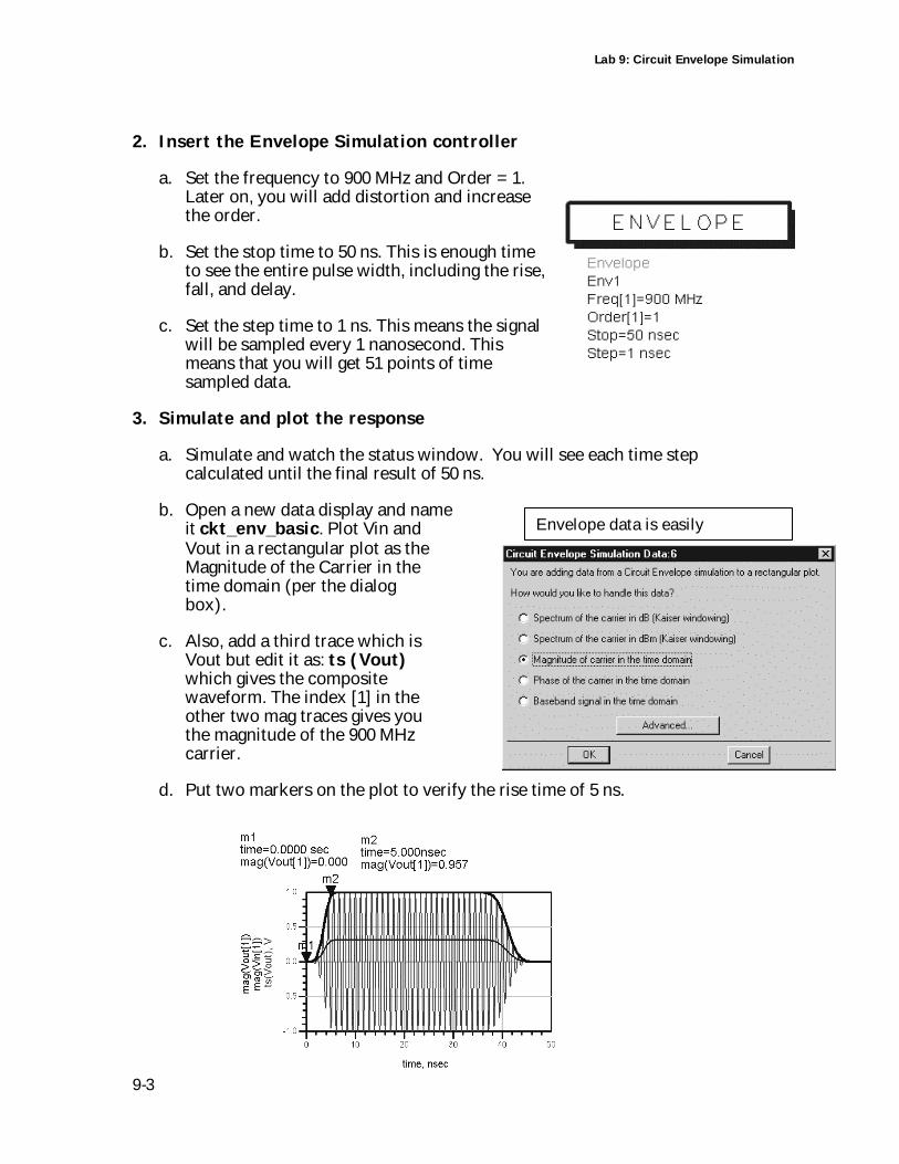
Lab 9: Circuit Envelope Simulation
9-3
2. Insert the Envelope Simulation controller
a. Set the frequency to 900 MHz and Order = 1.Later on, you will add distortion and increasethe order.
b. Set the stop time to 50 ns. This is enough timeto see the entire pulse width, including the rise,fall, and delay.
c. Set the step time to 1 ns. This means the signalwill be sampled every 1 nanosecond. Thismeans that you will get 51 points of timesampled data.
3. Simulate and plot the response
a. Simulate and watch the status window. You will see each time stepcalculated until the final result of 50 ns.
b. Open a new data display and nameit ckt_env_basic. Plot Vin andVout in a rectangular plot as theMagnitude of the Carrier in thetime domain (per the dialogbox).
c. Also, add a third trace which isVout but edit it as: ts (Vout)which gives the compositewaveform. The index [1] in theother two mag traces gives youthe magnitude of the 900 MHzcarrier.
d. Put two markers on the plot to verify the rise time of 5 ns.
Envelope data is easilydisplayed:
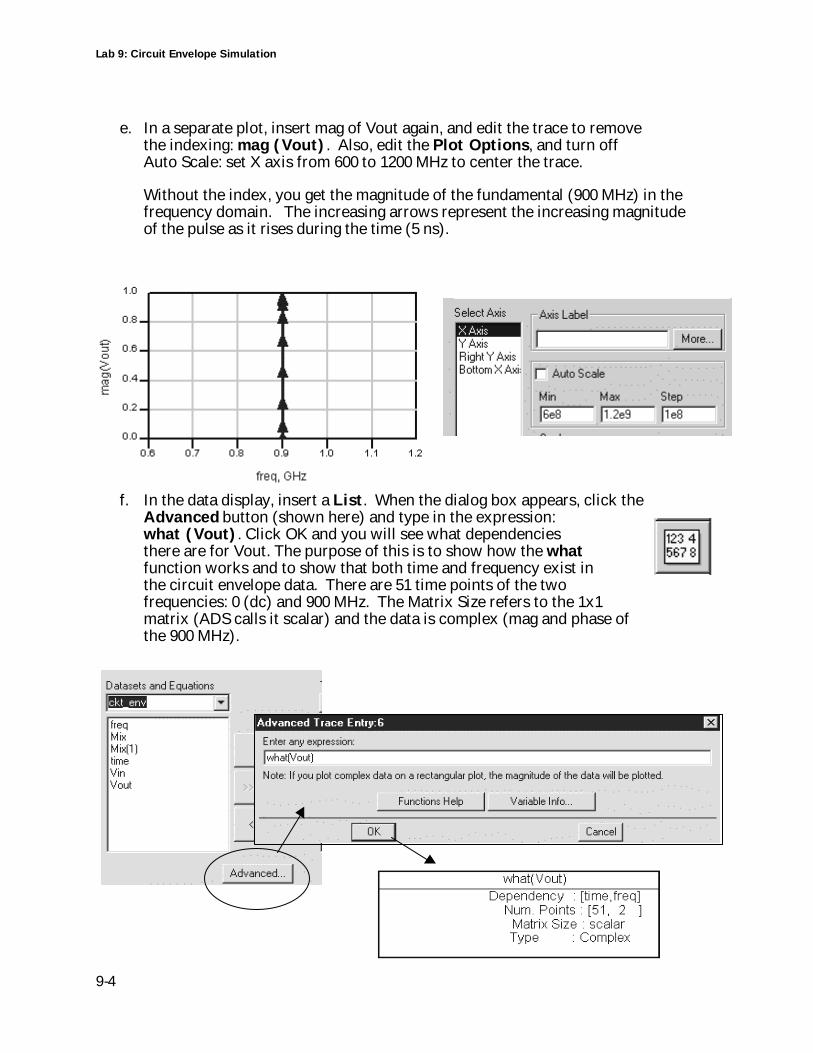
Lab 9: Circuit Envelope Simulation
9-4
e. In a separate plot, insert mag of Vout again, and edit the trace to removethe indexing: mag (Vout). Also, edit the Plot Options, and turn offAuto Scale: set X axis from 600 to 1200 MHz to center the trace.
Without the index, you get the magnitude of the fundamental (900 MHz) in thefrequency domain. The increasing arrows represent the increasing magnitudeof the pulse as it rises during the time (5 ns).
f. In the data display, insert a List. When the dialog box appears, click theAdvanced button (shown here) and type in the expression:what (Vout). Click OK and you will see what dependenciesthere are for Vout. The purpose of this is to show how the whatfunction works and to show that both time and frequency exist inthe circuit envelope data. There are 51 time points of the twofrequencies: 0 (dc) and 900 MHz. The Matrix Size refers to the 1x1matrix (ADS calls it scalar) and the data is complex (mag and phase ofthe 900 MHz).
Lab 9: Circuit Envelope Simulation
9-5
4. Set the envelope controller time step to 10 ns and simulate
Watch the results. The only thing you changed was the sampling rate butthe envelope now looks different because it was not sampled with enoughresolution. Simply because the time step is greater than the rise time. Onthe plot, you see the X axis has been increased and the markers are on thefirst two time points: 0 and10 nsec.
Note on Circuit Envelope sampling: In practice, the time step must bebased on the rise time or the modulation bandwidth. For rise time, the timestep can be: (rise time / 5) or less. Based on BW (modulation bandwidth)use 1 / (5x BW) to include distortion effects or side-bands. You could use10x but this would take more computation time. Sometimes, it may benecessary. Now, the next steps will test this theory.
5. Add distortion to the behavioral amplifier
a. Edit the Amplifier by setting: GainCompression Power = 5 (dbm is thedefault) and Gain Compression = 1dB. Ofcourse, these are not realistic values but itillustrates the point. Be sure to displaythese settings (good practice).
b. Set the controller order = 5 and keep thetime step at 10 ns. Also, set the source inputpower to 10 dbm: dbmtow (10).
Lab 9: Circuit Envelope Simulation
9-6
c. Simulate and view the data. Put the frequency domain plot X-axisback to Auto Scale and try to place the markers as shown. As you cansee, there are strong odd harmonics due to the amplifier distortion,which are summing out-of-phase. This results in the envelope amplitudebeing smaller than the magnitude of the Vin or Vout magnitude. Also,the envelope shape is not accurate because the sampling rate is toocoarse for the rise time of the Vin signal:
d. Set the time step to 1 ns andSimulate again. After thesimulation, the data willupdate and you will get anaccurate representation of theenvelope. Also, themagnitude of fundamental ofVin and Vout are still greaterthan the envelope magnitude,due to amplifier compression.
e. Insert a List of Vout. Scrolldown to the 5 nanosecond data.Now, you can see that the thirdhamonic is 180 degrees out-of-phase, making the envelopesmaller than the magnitude ofthe fundamental.
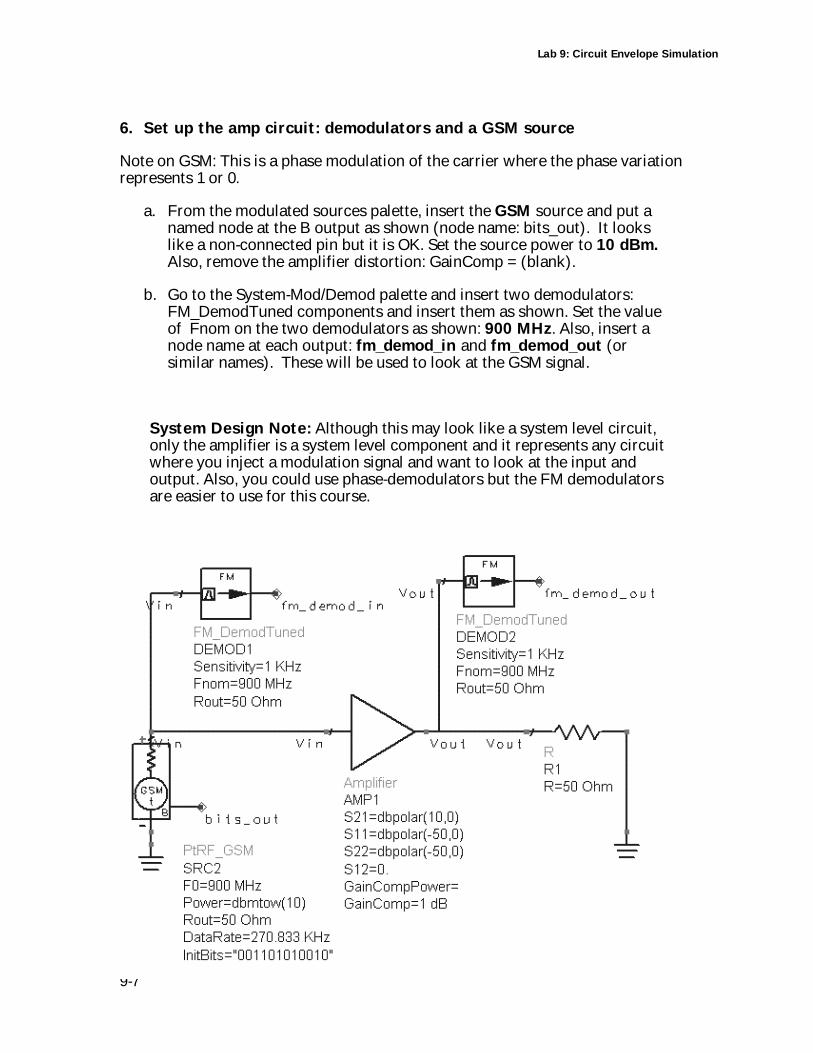
Lab 9: Circuit Envelope Simulation
9-7
6. Set up the amp circuit: demodulators and a GSM source
Note on GSM: This is a phase modulation of the carrier where the phase variationrepresents 1 or 0.
a. From the modulated sources palette, insert the GSM source and put anamed node at the B output as shown (node name: bits_out). It lookslike a non-connected pin but it is OK. Set the source power to 10 dBm.Also, remove the amplifier distortion: GainComp = (blank).
b. Go to the System-Mod/Demod palette and insert two demodulators:FM_DemodTuned components and insert them as shown. Set the valueof Fnom on the two demodulators as shown: 900 MHz. Also, insert anode name at each output: fm_demod_in and fm_demod_out (orsimilar names). These will be used to look at the GSM signal.
System Design Note: Although this may look like a system level circuit,only the amplifier is a system level component and it represents any circuitwhere you inject a modulation signal and want to look at the input andoutput. Also, you could use phase-demodulators but the FM demodulatorsare easier to use for this course.
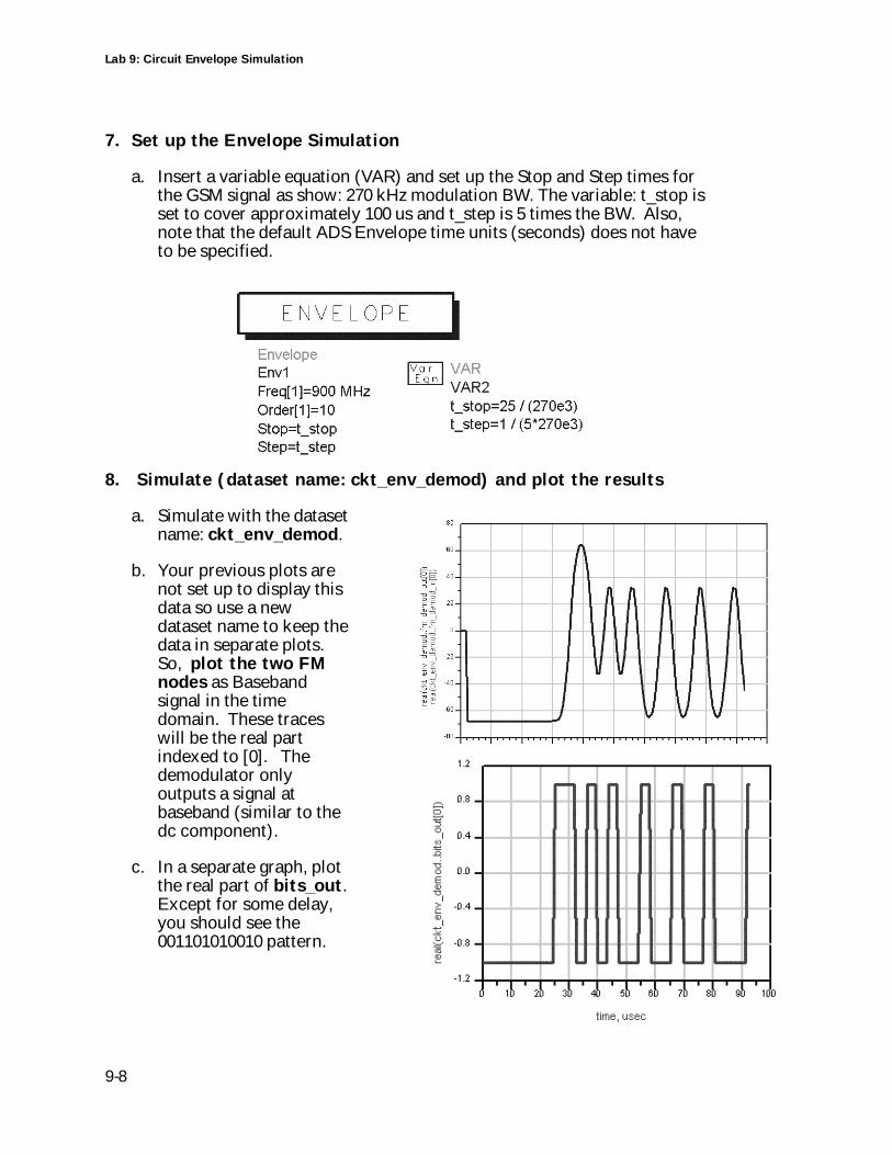
Lab 9: Circuit Envelope Simulation
9-8
7. Set up the Envelope Simulation
a. Insert a variable equation (VAR) and set up the Stop and Step times forthe GSM signal as show: 270 kHz modulation BW. The variable: t_stop isset to cover approximately 100 us and t_step is 5 times the BW. Also,note that the default ADS Envelope time units (seconds) does not haveto be specified.
8. Simulate (dataset name: ckt_env_demod) and plot the results
a. Simulate with the datasetname: ckt_env_demod.
b. Your previous plots arenot set up to display thisdata so use a newdataset name to keep thedata in separate plots.So, plot the two FMnodes as Basebandsignal in the timedomain. These traceswill be the real partindexed to [0]. Thedemodulator onlyoutputs a signal atbaseband (similar to thedc component).
c. In a separate graph, plotthe real part of bits_out.Except for some delay,you should see the001101010010 pattern.
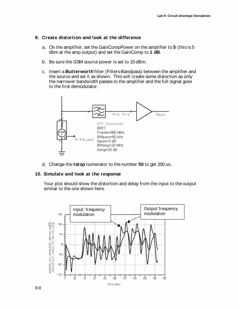
Lab 9: Circuit Envelope Simulation
9-9
9. Create distortion and look at the difference
a. On the amplifier, set the GainCompPower on the amplifier to 5 (this is 5dbm at the amp output) and set the GainComp to 1 dB.
b. Be sure the GSM source power is set to 10 dBm.
c. Insert a Butterworth filter (Filters-Bandpass) between the amplifier andthe source and set it as shown. This will create some distortion as onlythe narrower bandwidth passes to the amplifier and the full signal goesto the first demodulator.
d. Change the tstop numerator to the number 50 to get 200 us.
10. Simulate and look at the response
Your plot should show the distortion and delay from the input to the outputsimilar to the one shown here.
Output frequencymodulation
Input: frequencymodulation
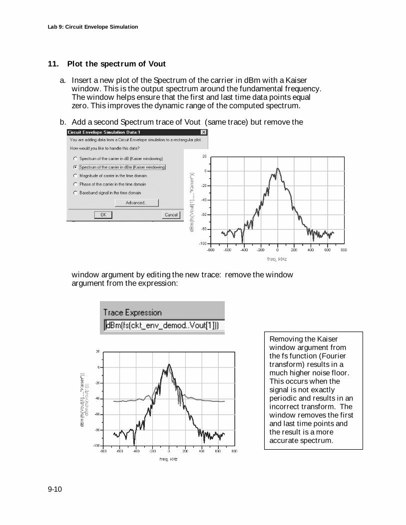
Lab 9: Circuit Envelope Simulation
9-10
11. Plot the spectrum of Vout
a. Insert a new plot of the Spectrum of the carrier in dBm with a Kaiserwindow. This is the output spectrum around the fundamental frequency.The window helps ensure that the first and last time data points equalzero. This improves the dynamic range of the computed spectrum.
b. Add a second Spectrum trace of Vout (same trace) but remove the
window argument by editing the new trace: remove the windowargument from the expression:
Removing the Kaiserwindow argument fromthe fs function (Fouriertransform) results in amuch higher noise floor.This occurs when thesignal is not exactlyperiodic and results in anincorrect transform. Thewindow removes the firstand last time points andthe result is a moreaccurate spectrum.
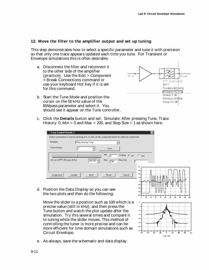
Lab 9: Circuit Envelope Simulation
9-11
12. Move the filter to the amplifier output and set up tuning
This step demonstrates how to select a specific parameter and tune it with precisionso that only one trace appears updated each time you tune. For Transient orEnvelope simulations this is often desirable.
a. Disconnect the filter and reconnect itto the other side of the amplifier(practice). Use the Edit > Component> Break Connections command oruse your keyboard Hot Key if it is setfor this command.
b. Start the Tune Mode and position thecursor on the 50 kHz value of theBWpass parameter and select it. Youshould see it appear on the Tune controller.
c. Click the Details button and set: Simulate: After pressing Tune, TraceHistory: 0, Min = 0 and Max = 200, and Step Size = 1 as shown here.
d. Position the Data Display so you can seethe two plots and then do the following:
Move the slider to a position such as 100 which is aprecise value (still in kHz), and then press theTune button and watch the plot update after thesimulation. Try this several times and compare itto tuning while the slider moves. This method ofcontrolling the tuner is more precise and can bemore efficient for time domain simulations such asCircuit Envelope.
e. As always, save the schematic and data display.
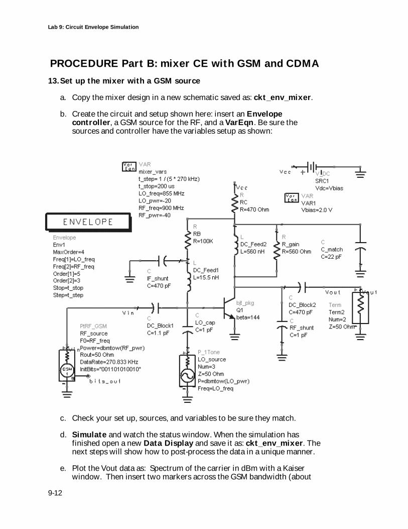
Lab 9: Circuit Envelope Simulation
9-12
PROCEDURE Part B: mixer CE with GSM and CDMA
13. Set up the mixer with a GSM source
a. Copy the mixer design in a new schematic saved as: ckt_env_mixer.
b. Create the circuit and setup shown here: insert an Envelopecontroller, a GSM source for the RF, and a VarEqn. Be sure thesources and controller have the variables setup as shown:
c. Check your set up, sources, and variables to be sure they match.
d. Simulate and watch the status window. When the simulation hasfinished open a new Data Display and save it as: ckt_env_mixer. Thenext steps will show how to post-process the data in a unique manner.
e. Plot the Vout data as: Spectrum of the carrier in dBm with a Kaiserwindow. Then insert two markers across the GSM bandwidth (about
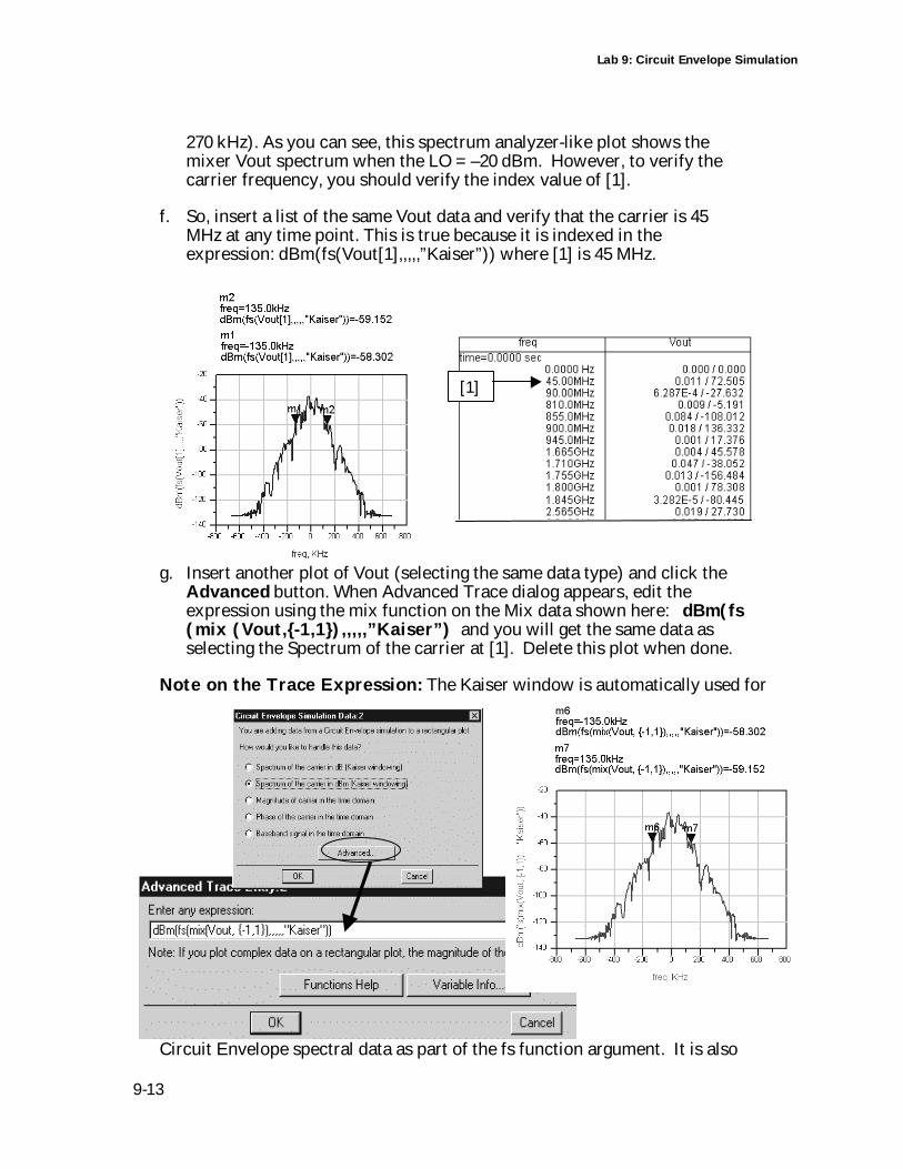
Lab 9: Circuit Envelope Simulation
9-13
270 kHz). As you can see, this spectrum analyzer-like plot shows themixer Vout spectrum when the LO = –20 dBm. However, to verify thecarrier frequency, you should verify the index value of [1].
f. So, insert a list of the same Vout data and verify that the carrier is 45MHz at any time point. This is true because it is indexed in theexpression: dBm(fs(Vout[1],,,,,”Kaiser”)) where [1] is 45 MHz.
g. Insert another plot of Vout (selecting the same data type) and click theAdvanced button. When Advanced Trace dialog appears, edit theexpression using the mix function on the Mix data shown here: dBm(fs(mix (Vout,{-1,1}),,,,,”Kaiser”) and you will get the same data asselecting the Spectrum of the carrier at [1]. Delete this plot when done.
Note on the Trace Expression: The Kaiser window is automatically used for
Circuit Envelope spectral data as part of the fs function argument. It is also
[1]
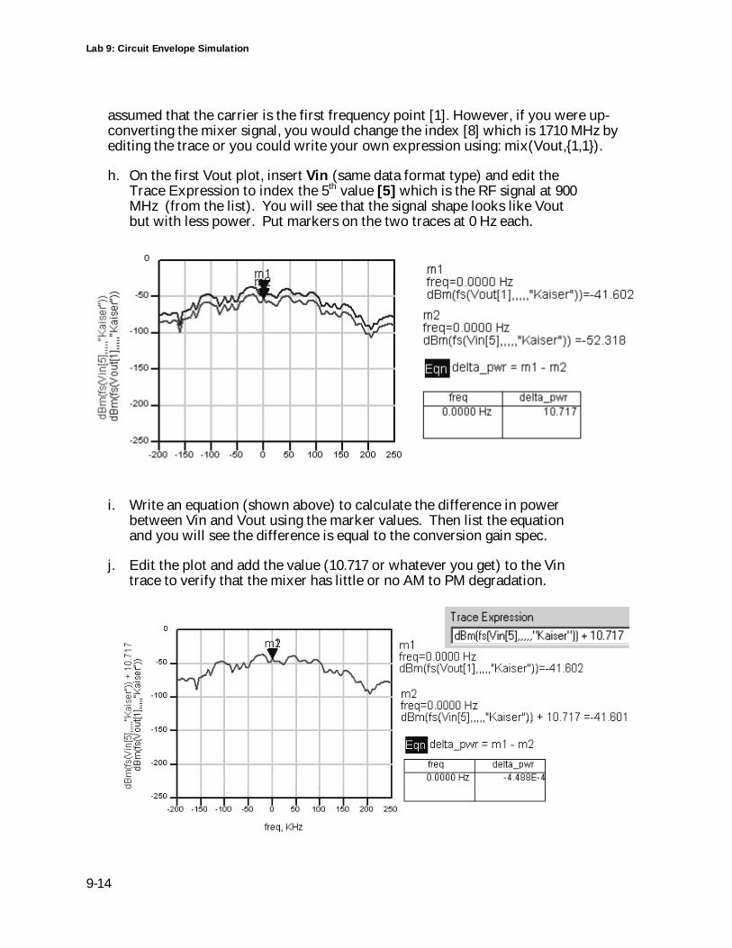
Lab 9: Circuit Envelope Simulation
9-14
assumed that the carrier is the first frequency point [1]. However, if you were up-converting the mixer signal, you would change the index [8] which is 1710 MHz byediting the trace or you could write your own expression using: mix(Vout,{1,1}).
h. On the first Vout plot, insert Vin (same data format type) and edit theTrace Expression to index the 5th value [5] which is the RF signal at 900MHz (from the list). You will see that the signal shape looks like Voutbut with less power. Put markers on the two traces at 0 Hz each.
i. Write an equation (shown above) to calculate the difference in powerbetween Vin and Vout using the marker values. Then list the equationand you will see the difference is equal to the conversion gain spec.
j. Edit the plot and add the value (10.717 or whatever you get) to the Vintrace to verify that the mixer has little or no AM to PM degradation.
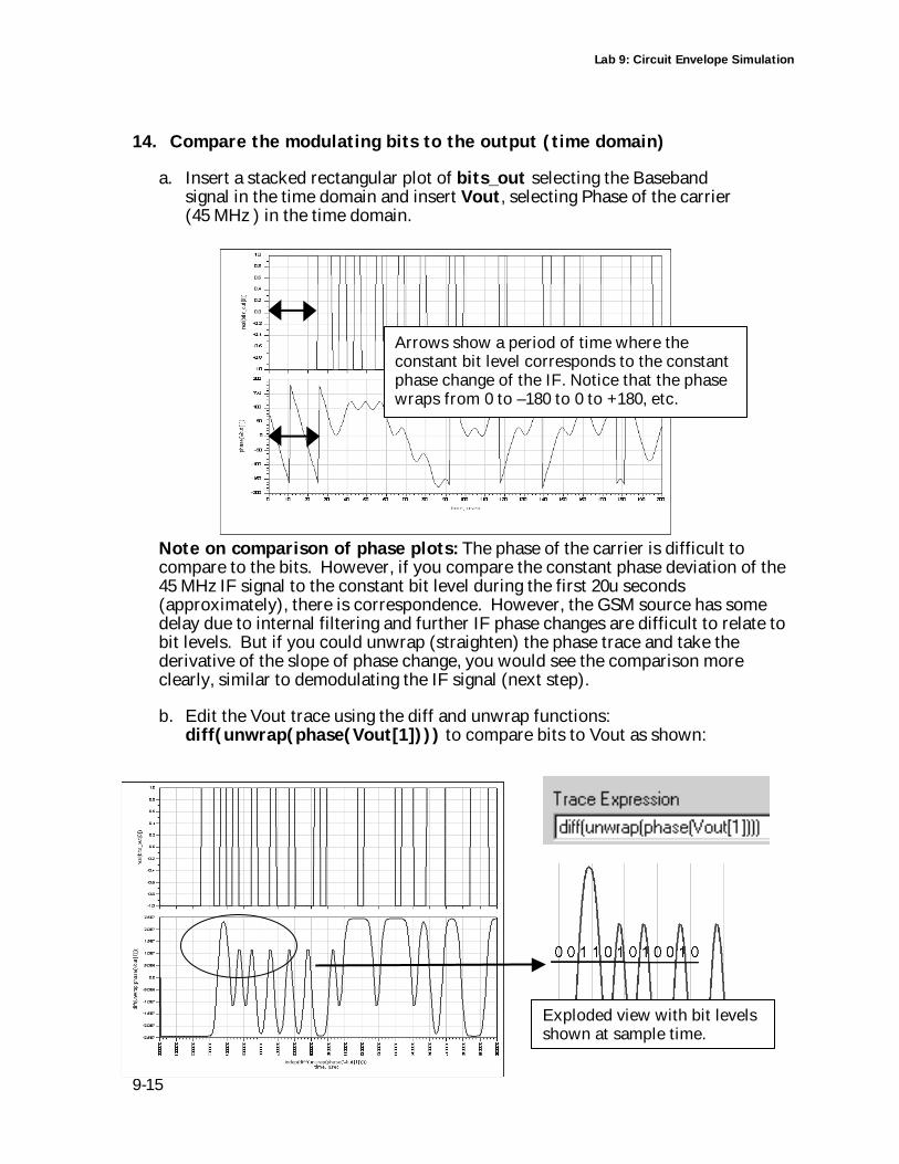
Lab 9: Circuit Envelope Simulation
9-15
14. Compare the modulating bits to the output (time domain)
a. Insert a stacked rectangular plot of bits_out selecting the Basebandsignal in the time domain and insert Vout, selecting Phase of the carrier(45 MHz ) in the time domain.
Note on comparison of phase plots: The phase of the carrier is difficult tocompare to the bits. However, if you compare the constant phase deviation of the45 MHz IF signal to the constant bit level during the first 20u seconds(approximately), there is correspondence. However, the GSM source has somedelay due to internal filtering and further IF phase changes are difficult to relate tobit levels. But if you could unwrap (straighten) the phase trace and take thederivative of the slope of phase change, you would see the comparison moreclearly, similar to demodulating the IF signal (next step).
b. Edit the Vout trace using the diff and unwrap functions:diff(unwrap(phase(Vout[1]))) to compare bits to Vout as shown:
Arrows show a period of time where theconstant bit level corresponds to the constantphase change of the IF. Notice that the phasewraps from 0 to –180 to 0 to +180, etc.
Exploded view with bit levelsshown at sample time.
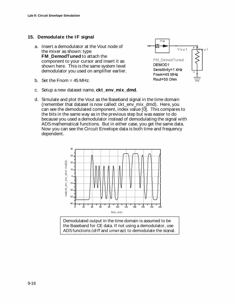
Lab 9: Circuit Envelope Simulation
9-16
15. Demodulate the IF signal
a. Insert a demodulator at the Vout node ofthe mixer as shown: typeFM_DemodTuned to attach thecomponent to your cursor and insert it asshown here. This is the same system leveldemodulator you used on amplifier earlier.
b. Set the Fnom = 45 MHz.
c. Setup a new dataset name, ckt_env_mix_dmd.
d. Simulate and plot the Vout as the Baseband signal in the time domain(remember that dataset is now called: ckt_env_mix_dmd). Here, youcan see the demodulated component, index value [0]. This compares tothe bits in the same way as in the previous step but was easier to dobecause you used a demodulator instead of demodulating the signal withADS mathematical functions. But in either case, you get the same data.Now you can see the Circuit Envelope data is both time and frequencydependent.
Demodulated output in the time domain is assumed to bethe Baseband for CE data. If not using a demodulator, useADS functions (diff and unwrap) to demodulate the signal.
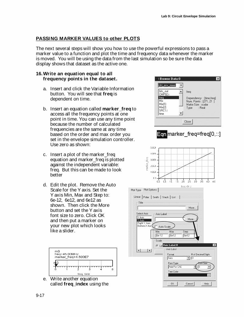
Lab 9: Circuit Envelope Simulation
9-17
PASSING MARKER VALUES to other PLOTS
The next several steps will show you how to use the powerful expressions to pass amarker value to a function and plot the time and frequency data whenever the markeris moved. You will be using the data from the last simulation so be sure the datadisplay shows that dataset as the active one.
16. Write an equation equal to allfrequency points in the dataset.
a. Insert and click the Variable Informationbutton. You will see that freq isdependent on time.
b. Insert an equation called marker_freq toaccess all the frequency points at onepoint in time. You can use any time pointbecause the number of calculatedfrequencies are the same at any timebased on the order and max order youset in the envelope simulation controller.Use zero as shown:
c. Insert a plot of the marker_freqequation and marker_freq is plottedagainst the independent variable:freq. But this can be made to lookbetter
d. Edit the plot. Remove the AutoScale for the Y axis. Set theY axis Min, Max and Step to:6e-12, 6e12, and 6e12 asshown. Then click the Morebutton and set the Y axisfont size to zero. Click OKand then put a marker onyour new plot which lookslike a slider.
e. Write another equationcalled freq_index using the
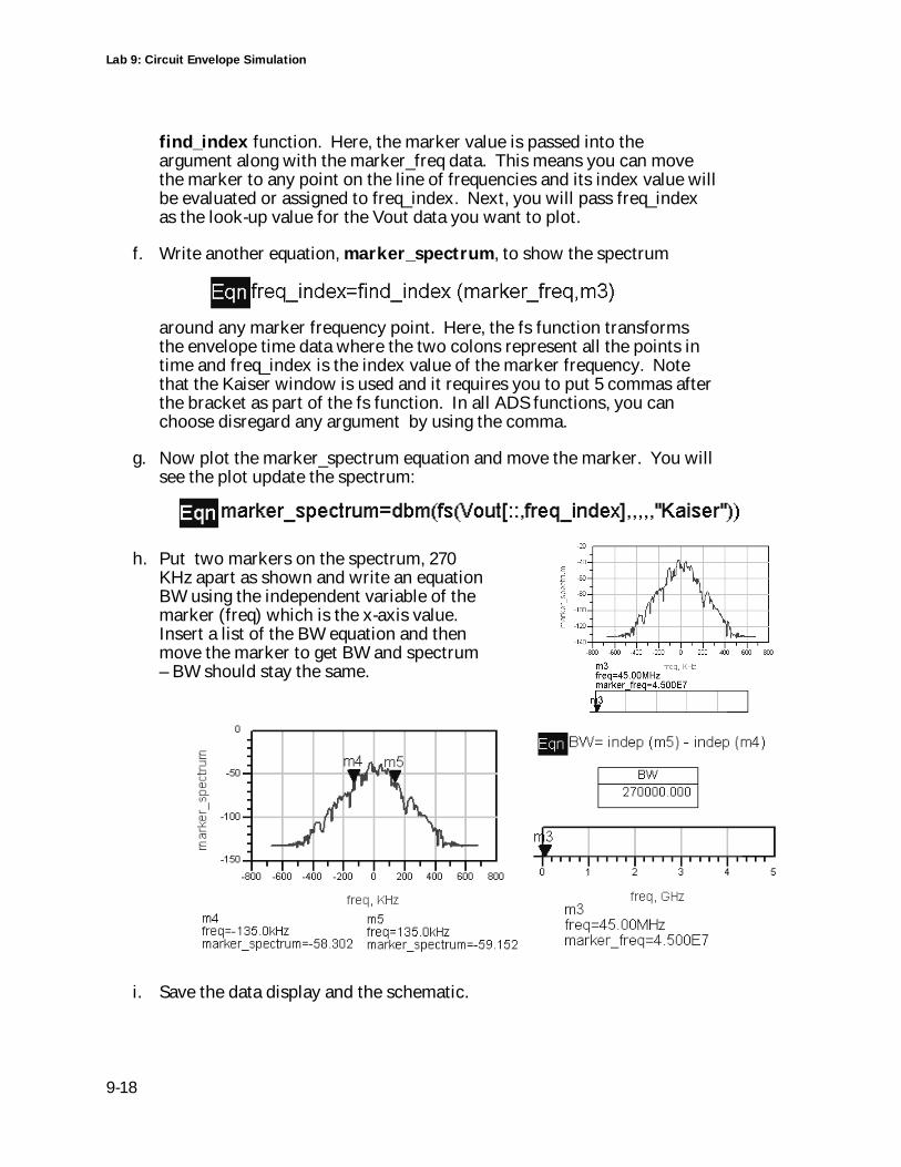
Lab 9: Circuit Envelope Simulation
9-18
find_index function. Here, the marker value is passed into theargument along with the marker_freq data. This means you can movethe marker to any point on the line of frequencies and its index value willbe evaluated or assigned to freq_index. Next, you will pass freq_indexas the look-up value for the Vout data you want to plot.
f. Write another equation, marker_spectrum, to show the spectrum
around any marker frequency point. Here, the fs function transformsthe envelope time data where the two colons represent all the points intime and freq_index is the index value of the marker frequency. Notethat the Kaiser window is used and it requires you to put 5 commas afterthe bracket as part of the fs function. In all ADS functions, you canchoose disregard any argument by using the comma.
g. Now plot the marker_spectrum equation and move the marker. You willsee the plot update the spectrum:
h. Put two markers on the spectrum, 270KHz apart as shown and write an equationBW using the independent variable of themarker (freq) which is the x-axis value.Insert a list of the BW equation and thenmove the marker to get BW and spectrum– BW should stay the same.
i. Save the data display and the schematic.
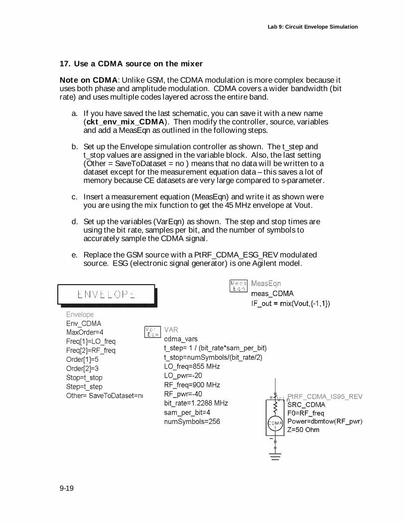
Lab 9: Circuit Envelope Simulation
9-19
17. Use a CDMA source on the mixer
Note on CDMA: Unlike GSM, the CDMA modulation is more complex because ituses both phase and amplitude modulation. CDMA covers a wider bandwidth (bitrate) and uses multiple codes layered across the entire band.
a. If you have saved the last schematic, you can save it with a new name(ckt_env_mix_CDMA). Then modify the controller, source, variablesand add a MeasEqn as outlined in the following steps.
b. Set up the Envelope simulation controller as shown. The t_step andt_stop values are assigned in the variable block. Also, the last setting(Other = SaveToDataset = no ) means that no data will be written to adataset except for the measurement equation data – this saves a lot ofmemory because CE datasets are very large compared to s-parameter.
c. Insert a measurement equation (MeasEqn) and write it as shown wereyou are using the mix function to get the 45 MHz envelope at Vout.
d. Set up the variables (VarEqn) as shown. The step and stop times areusing the bit rate, samples per bit, and the number of symbols toaccurately sample the CDMA signal.
e. Replace the GSM source with a PtRF_CDMA_ESG_REV modulatedsource. ESG (electronic signal generator) is one Agilent model.
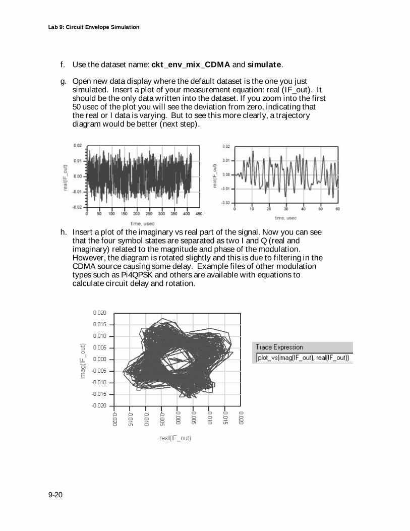
Lab 9: Circuit Envelope Simulation
9-20
f. Use the dataset name: ckt_env_mix_CDMA and simulate.
g. Open new data display where the default dataset is the one you justsimulated. Insert a plot of your measurement equation: real (IF_out). Itshould be the only data written into the dataset. If you zoom into the first50 usec of the plot you will see the deviation from zero, indicating thatthe real or I data is varying. But to see this more clearly, a trajectorydiagram would be better (next step).
h. Insert a plot of the imaginary vs real part of the signal. Now you can seethat the four symbol states are separated as two I and Q (real andimaginary) related to the magnitude and phase of the modulation.However, the diagram is rotated slightly and this is due to filtering in theCDMA source causing some delay. Example files of other modulationtypes such as Pi4QPSK and others are available with equations tocalculate circuit delay and rotation.
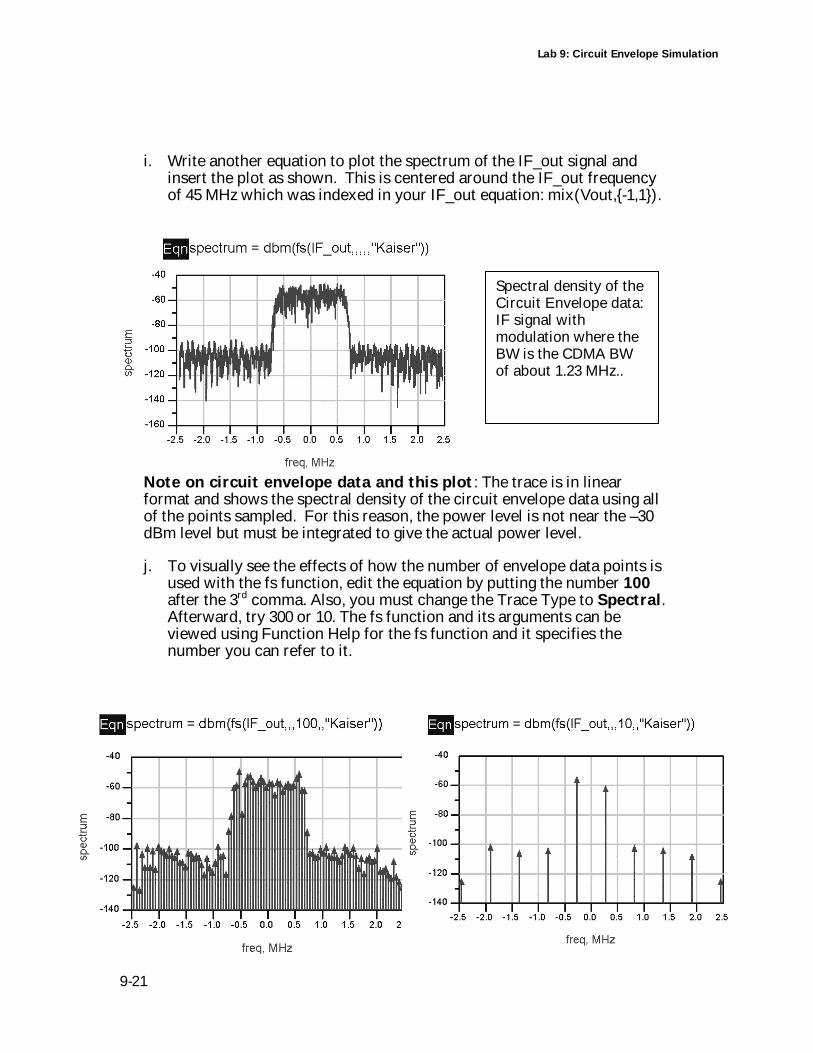
Lab 9: Circuit Envelope Simulation
9-21
i. Write another equation to plot the spectrum of the IF_out signal andinsert the plot as shown. This is centered around the IF_out frequencyof 45 MHz which was indexed in your IF_out equation: mix(Vout,{-1,1}).
Note on circuit envelope data and this plot: The trace is in linearformat and shows the spectral density of the circuit envelope data using allof the points sampled. For this reason, the power level is not near the –30dBm level but must be integrated to give the actual power level.
j. To visually see the effects of how the number of envelope data points isused with the fs function, edit the equation by putting the number 100after the 3rd comma. Also, you must change the Trace Type to Spectral.Afterward, try 300 or 10. The fs function and its arguments can beviewed using Function Help for the fs function and it specifies thenumber you can refer to it.
Spectral density of theCircuit Envelope data:IF signal withmodulation where theBW is the CDMA BWof about 1.23 MHz..
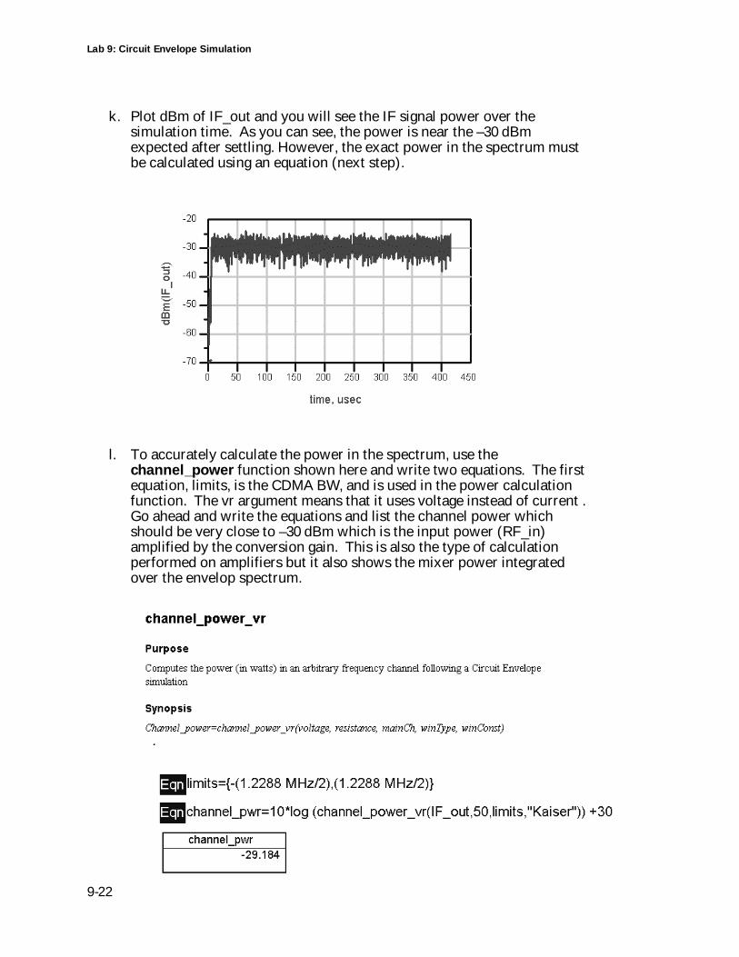
Lab 9: Circuit Envelope Simulation
9-22
k. Plot dBm of IF_out and you will see the IF signal power over thesimulation time. As you can see, the power is near the –30 dBmexpected after settling. However, the exact power in the spectrum mustbe calculated using an equation (next step).
l. To accurately calculate the power in the spectrum, use thechannel_power function shown here and write two equations. The firstequation, limits, is the CDMA BW, and is used in the power calculationfunction. The vr argument means that it uses voltage instead of current .Go ahead and write the equations and list the channel power whichshould be very close to –30 dBm which is the input power (RF_in)amplified by the conversion gain. This is also the type of calculationperformed on amplifiers but it also shows the mixer power integratedover the envelop spectrum.
Lab 9: Circuit Envelope Simulation
9-23
EXTRA EXERCISES:
1. Sweep LO power and watch the change in the output.
2. Use the demodulator on the output and re-run the simulations.
3. Go to the example file: examples\Tutorial\ModSources_prj\Pi4DQPSK and copythe source and data display into your directory and try that source on the mixer,using the data display as a reference to guide you.
4. Put the filter the output and re-run the simulations.

Lab 9: Circuit Envelope Simulation
9-24
THIS PAGE LEFT INTENTIONALLY BLANK
10
This chapter shows how to use LineCalc and the Transientsimulator to make basic delay and TDR measurements.
Lab 10: TDR and LineCalc
with the Transient Simulator
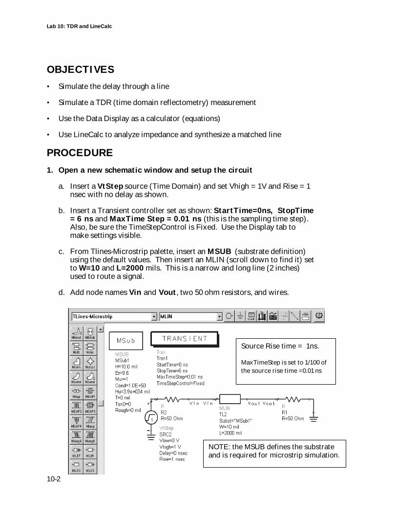
Lab 10: TDR and LineCalc
10-2
OBJECTIVES
• Simulate the delay through a line
• Simulate a TDR (time domain reflectometry) measurement
• Use the Data Display as a calculator (equations)
• Use LineCalc to analyze impedance and synthesize a matched line
PROCEDURE
1. Open a new schematic window and setup the circuit
a. Insert a VtStep source (Time Domain) and set Vhigh = 1V and Rise = 1nsec with no delay as shown.
b. Insert a Transient controller set as shown: StartTime=0ns, StopTime= 6 ns and MaxTime Step = 0.01 ns (this is the sampling time step).Also, be sure the TimeStepControl is Fixed. Use the Display tab tomake settings visible.
c. From Tlines-Microstrip palette, insert an MSUB (substrate definition)using the default values. Then insert an MLIN (scroll down to find it) setto W=10 and L=2000 mils. This is a narrow and long line (2 inches)used to route a signal.
d. Add node names Vin and Vout, two 50 ohm resistors, and wires.
NOTE: the MSUB defines the substrateand is required for microstrip simulation.
Source Rise time = 1ns.
MaxTimeStep is set to 1/100 ofthe source rise time =0.01 ns
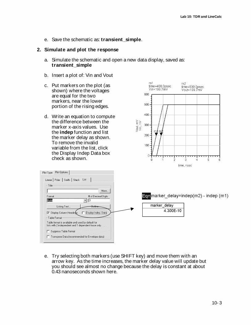
Lab 10: TDR and LineCalc
310-
e. Save the schematic as: transient_simple.
2. Simulate and plot the response
a. Simulate the schematic and open a new data display, saved as:transient_simple
b. Insert a plot of: Vin and Vout
c. Put markers on the plot (asshown) where the voltagesare equal for the twomarkers, near the lowerportion of the rising edges.
d. Write an equation to computethe difference between themarker x-axis values. Usethe indep function and listthe marker delay as shown.To remove the invalidvariable from the list, clickthe Display Indep Data boxcheck as shown.
e. Try selecting both markers (use SHIFT key) and move them with anarrow key. As the time increases, the marker delay value will update butyou should see almost no change because the delay is constant at about0.43 nanoseconds shown here.
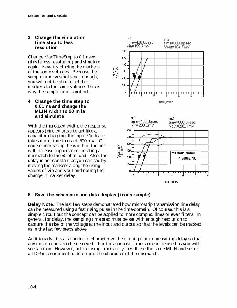
Lab 10: TDR and LineCalc
10-4
3. Change the simulationtime step to lessresolution
Change MaxTimeStep to 0.1 nsec(this is less resolution) and simulateagain. Now try placing the markersat the same voltages. Because thesample time was not small enough,you will not be able to set themarkers to the same voltage. This iswhy the sample time is critical.
4. Change the time step to0.01 ns and change theMLIN width to 20 milsand simulate
With the increased width, the responseappears (circled area) to act like acapacitor charging: the input Vin tracetakes more time to reach 500 mV. Ofcourse, increasing the width of the linewill increase capacitance, creating amismatch to the 50 ohm load. Also, thedelay is not constant as you can see bymoving the markers along the risingvalues of Vin and Vout and noting thechange in marker delay.
5. Save the schematic and data display (trans_simple)
Delay Note: The last few steps demonstrated how microstrip transmission line delaycan be measured using a fast rising pulse in the time-domain. Of course, this is asimple circuit but the concept can be applied to more complex lines or even filters. Ingeneral, for delay, the sampling time step must be set with enough resolution tocapture the rise of the voltage at the input and output so that the levels can be trackedas in the last few steps above.
Additionally, it is also better to characterize the circuit prior to measuring delay so thatany mismatches can be resolved. For this purpose, LineCalc can be used as you willsee later on. However, before using LineCalc, you will use the same MLIN and set upa TDR measurement to determine the character of the mismatch.
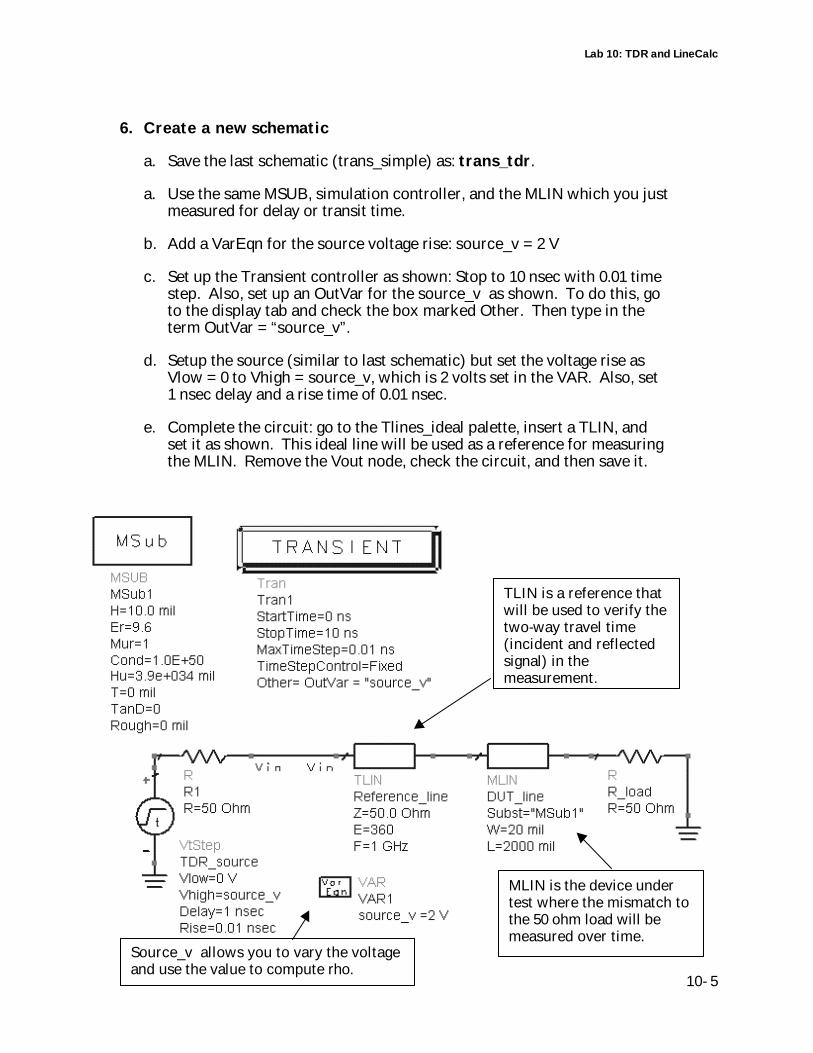
Lab 10: TDR and LineCalc
510-
6. Create a new schematic
a. Save the last schematic (trans_simple) as: trans_tdr.
a. Use the same MSUB, simulation controller, and the MLIN which you justmeasured for delay or transit time.
b. Add a VarEqn for the source voltage rise: source_v = 2 V
c. Set up the Transient controller as shown: Stop to 10 nsec with 0.01 timestep. Also, set up an OutVar for the source_v as shown. To do this, goto the display tab and check the box marked Other. Then type in theterm OutVar = “source_v”.
d. Setup the source (similar to last schematic) but set the voltage rise asVlow = 0 to Vhigh = source_v, which is 2 volts set in the VAR. Also, set1 nsec delay and a rise time of 0.01 nsec.
e. Complete the circuit: go to the Tlines_ideal palette, insert a TLIN, andset it as shown. This ideal line will be used as a reference for measuringthe MLIN. Remove the Vout node, check the circuit, and then save it.
TLIN is a reference thatwill be used to verify thetwo-way travel time(incident and reflectedsignal) in themeasurement.
MLIN is the device undertest where the mismatch tothe 50 ohm load will bemeasured over time.
Source_v allows you to vary the voltageand use the value to compute rho.
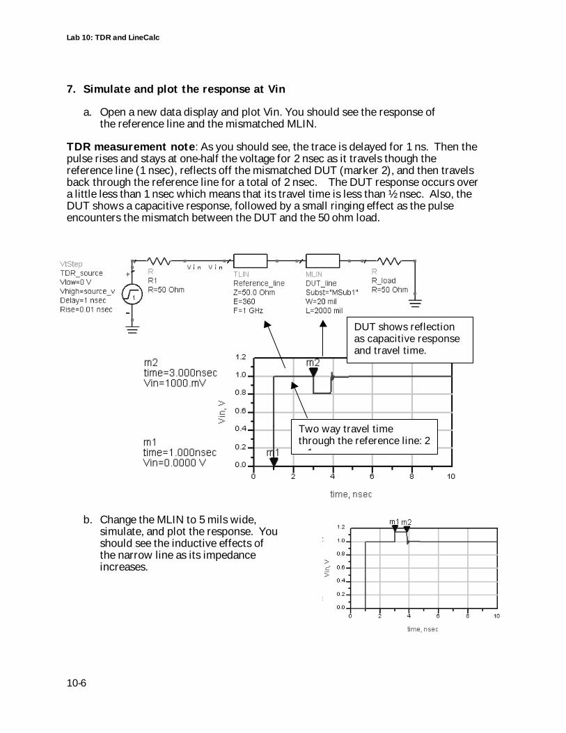
Lab 10: TDR and LineCalc
10-6
7. Simulate and plot the response at Vin
a. Open a new data display and plot Vin. You should see the response ofthe reference line and the mismatched MLIN.
TDR measurement note: As you should see, the trace is delayed for 1 ns. Then thepulse rises and stays at one-half the voltage for 2 nsec as it travels though thereference line (1 nsec), reflects off the mismatched DUT (marker 2), and then travelsback through the reference line for a total of 2 nsec. The DUT response occurs overa little less than 1 nsec which means that its travel time is less than ½ nsec. Also, theDUT shows a capacitive response, followed by a small ringing effect as the pulseencounters the mismatch between the DUT and the 50 ohm load.
b. Change the MLIN to 5 mils wide,simulate, and plot the response. Youshould see the inductive effects ofthe narrow line as its impedanceincreases.
Two way travel timethrough the reference line: 2x 1 nsec.
DUT shows reflectionas capacitive responseand travel time.
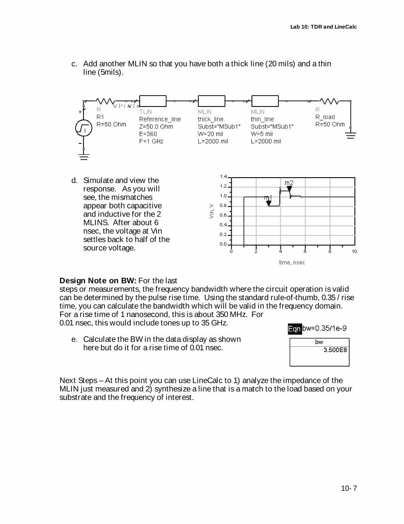
Lab 10: TDR and LineCalc
710-
c. Add another MLIN so that you have both a thick line (20 mils) and a thinline (5mils).
d. Simulate and view theresponse. As you willsee, the mismatchesappear both capacitiveand inductive for the 2MLINS. After about 6nsec, the voltage at Vinsettles back to half of thesource voltage.
Design Note on BW: For the laststeps or measurements, the frequency bandwidth where the circuit operation is validcan be determined by the pulse rise time. Using the standard rule-of-thumb, 0.35 / risetime, you can calculate the bandwidth which will be valid in the frequency domain.For a rise time of 1 nanosecond, this is about 350 MHz. For0.01 nsec, this would include tones up to 35 GHz.
e. Calculate the BW in the data display as shownhere but do it for a rise time of 0.01 nsec.
Next Steps – At this point you can use LineCalc to 1) analyze the impedance of theMLIN just measured and 2) synthesize a line that is a match to the load based on yoursubstrate and the frequency of interest.
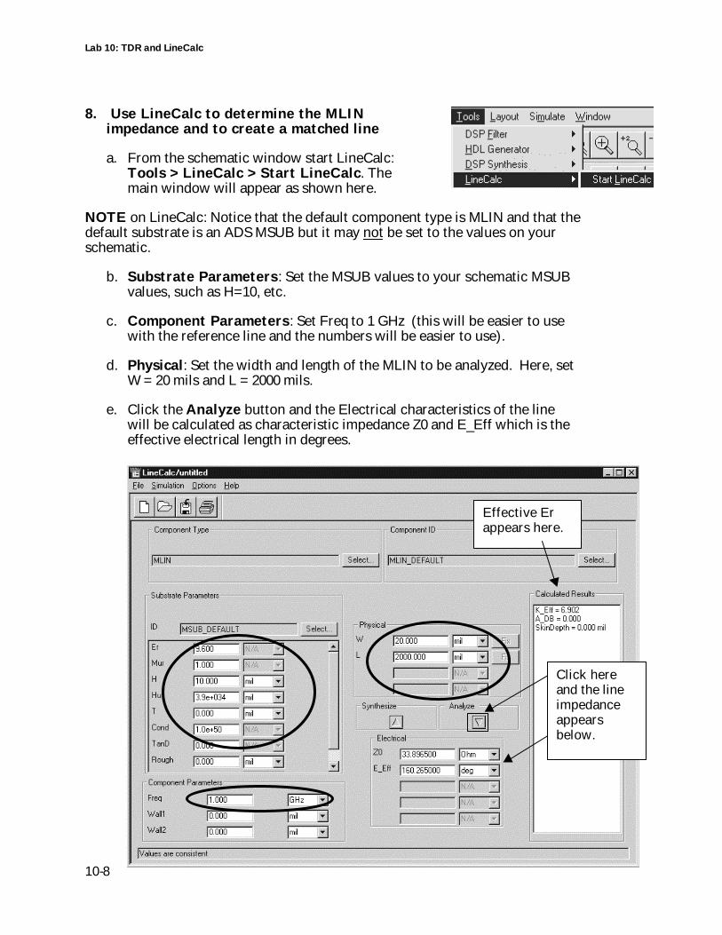
Lab 10: TDR and LineCalc
10-8
8. Use LineCalc to determine the MLINimpedance and to create a matched line
a. From the schematic window start LineCalc:Tools > LineCalc > Start LineCalc. Themain window will appear as shown here.
NOTE on LineCalc: Notice that the default component type is MLIN and that thedefault substrate is an ADS MSUB but it may not be set to the values on yourschematic.
b. Substrate Parameters: Set the MSUB values to your schematic MSUBvalues, such as H=10, etc.
c. Component Parameters: Set Freq to 1 GHz (this will be easier to usewith the reference line and the numbers will be easier to use).
d. Physical: Set the width and length of the MLIN to be analyzed. Here, setW = 20 mils and L = 2000 mils.
e. Click the Analyze button and the Electrical characteristics of the linewill be calculated as characteristic impedance Z0 and E_Eff which is theeffective electrical length in degrees.
Click hereand the lineimpedanceappearsbelow.
Effective Erappears here.
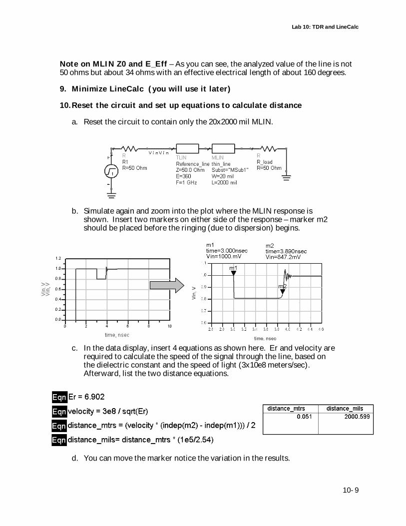
Lab 10: TDR and LineCalc
910-
Note on MLIN Z0 and E_Eff – As you can see, the analyzed value of the line is not50 ohms but about 34 ohms with an effective electrical length of about 160 degrees.
9. Minimize LineCalc (you will use it later)
10. Reset the circuit and set up equations to calculate distance
a. Reset the circuit to contain only the 20x2000 mil MLIN.
b. Simulate again and zoom into the plot where the MLIN response isshown. Insert two markers on either side of the response – marker m2should be placed before the ringing (due to dispersion) begins.
c. In the data display, insert 4 equations as shown here. Er and velocity arerequired to calculate the speed of the signal through the line, based onthe dielectric constant and the speed of light (3x10e8 meters/sec).Afterward, list the two distance equations.
d. You can move the marker notice the variation in the results.
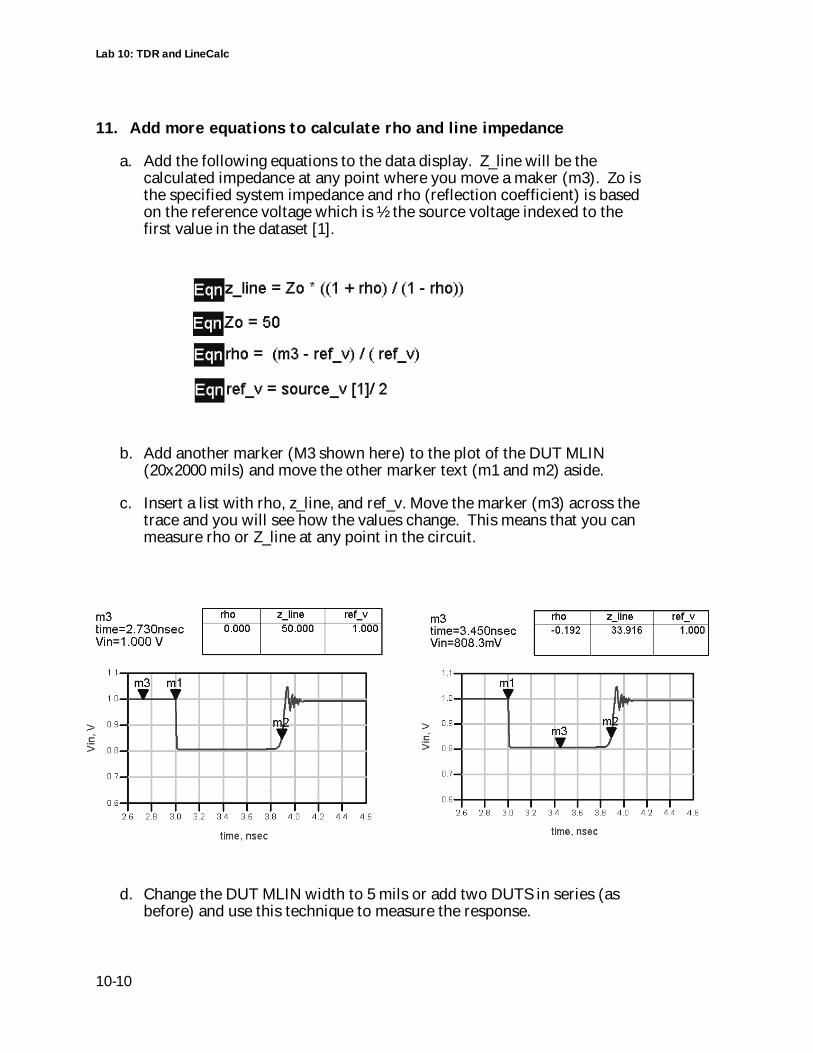
Lab 10: TDR and LineCalc
10-10
11. Add more equations to calculate rho and line impedance
a. Add the following equations to the data display. Z_line will be thecalculated impedance at any point where you move a maker (m3). Zo isthe specified system impedance and rho (reflection coefficient) is basedon the reference voltage which is ½ the source voltage indexed to thefirst value in the dataset [1].
b. Add another marker (M3 shown here) to the plot of the DUT MLIN(20x2000 mils) and move the other marker text (m1 and m2) aside.
c. Insert a list with rho, z_line, and ref_v. Move the marker (m3) across thetrace and you will see how the values change. This means that you canmeasure rho or Z_line at any point in the circuit.
d. Change the DUT MLIN width to 5 mils or add two DUTS in series (asbefore) and use this technique to measure the response.
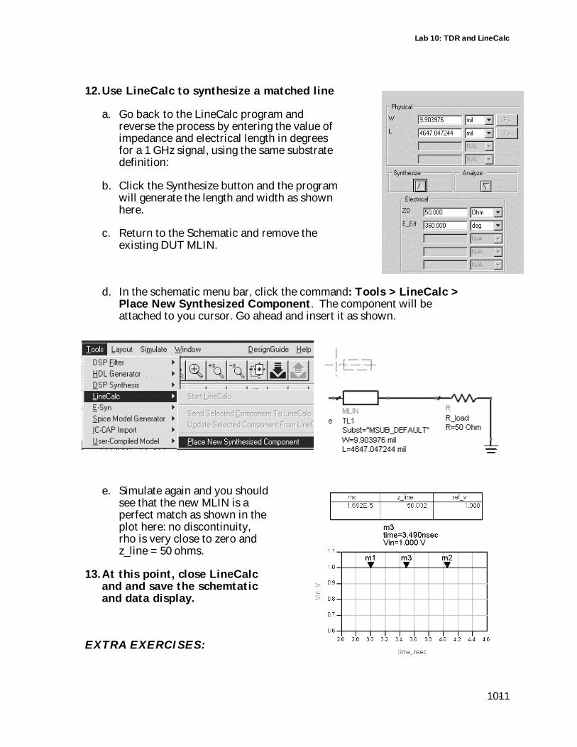
Lab 10: TDR and LineCalc
1110-
12. Use LineCalc to synthesize a matched line
a. Go back to the LineCalc program andreverse the process by entering the value ofimpedance and electrical length in degreesfor a 1 GHz signal, using the same substratedefinition:
b. Click the Synthesize button and the programwill generate the length and width as shownhere.
c. Return to the Schematic and remove theexisting DUT MLIN.
d. In the schematic menu bar, click the command: Tools > LineCalc >Place New Synthesized Component. The component will beattached to you cursor. Go ahead and insert it as shown.
e. Simulate again and you shouldsee that the new MLIN is aperfect match as shown in theplot here: no discontinuity,rho is very close to zero andz_line = 50 ohms.
13. At this point, close LineCalcand and save the schemtaticand data display.
EXTRA EXERCISES:
Lab 10: TDR and LineCalc
10-12
1. Insert several lengths of line into the existing schematic and measure the responseas in the lab steps: delay and TDR.
2. Create a filter using the microstrip components library and then measure the delayas in the first part of the lab.
3. Try writing an expression and listing VSWR: 1 + mag (rho) / 1 – mag (rho) for theMLIN of 20x2000 – it should be about 1.5.
4. Example file for TDR: Create a new project directory copy the example projectnamed RF_Board/TDRmeas_vs_model. Run the simulation and then change ortune the transmission line values (L and W) to see the response. Also, if you makeall W and L and H (lines and substrate) 1/10 of their values, you should get thesame results.
11
This chapter shows how to simulate various amplifiermeasurements for both low noise and power amplifiers.
Lab 11: Amplifier Simulations
OBJECTIVES
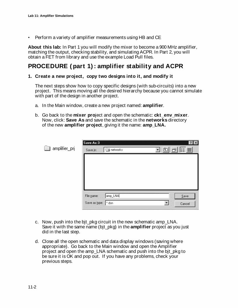
Lab 11: Amplifier Simulations
11-2
• Perform a variety of amplifier measurements using HB and CE
About this lab: In Part 1 you will modify the mixer to become a 900 MHz amplifier,matching the output, checking stability, and simulating ACPR. In Part 2, you willobtain a FET from library and use the example Load Pull files.
PROCEDURE (part 1): amplifier stability and ACPR
1. Create a new project, copy two designs into it, and modify it
The next steps show how to copy specific designs (with sub-circuits) into a newproject. This means moving all the desired hierarchy because you cannot simulatewith part of the design in another project.
a. In the Main window, create a new project named: amplifier.
b. Go back to the mixer project and open the schematic: ckt_env_mixer.Now, click: Save As and save the schematic in the networks directoryof the new amplifier project, giving it the name: amp_LNA.
c. Now, push into the bjt_pkg circuit in the new schematic amp_LNA.Save it with the same name (bjt_pkg) in the amplifier project as you justdid in the last step.
d. Close all the open schematic and data display windows (saving whereappropriate). Go back to the Main window and open the Amplifierproject and open the amp_LNA schematic and push into the bjt_pkg tobe sure it is OK and pop out. If you have any problems, check yourprevious steps.
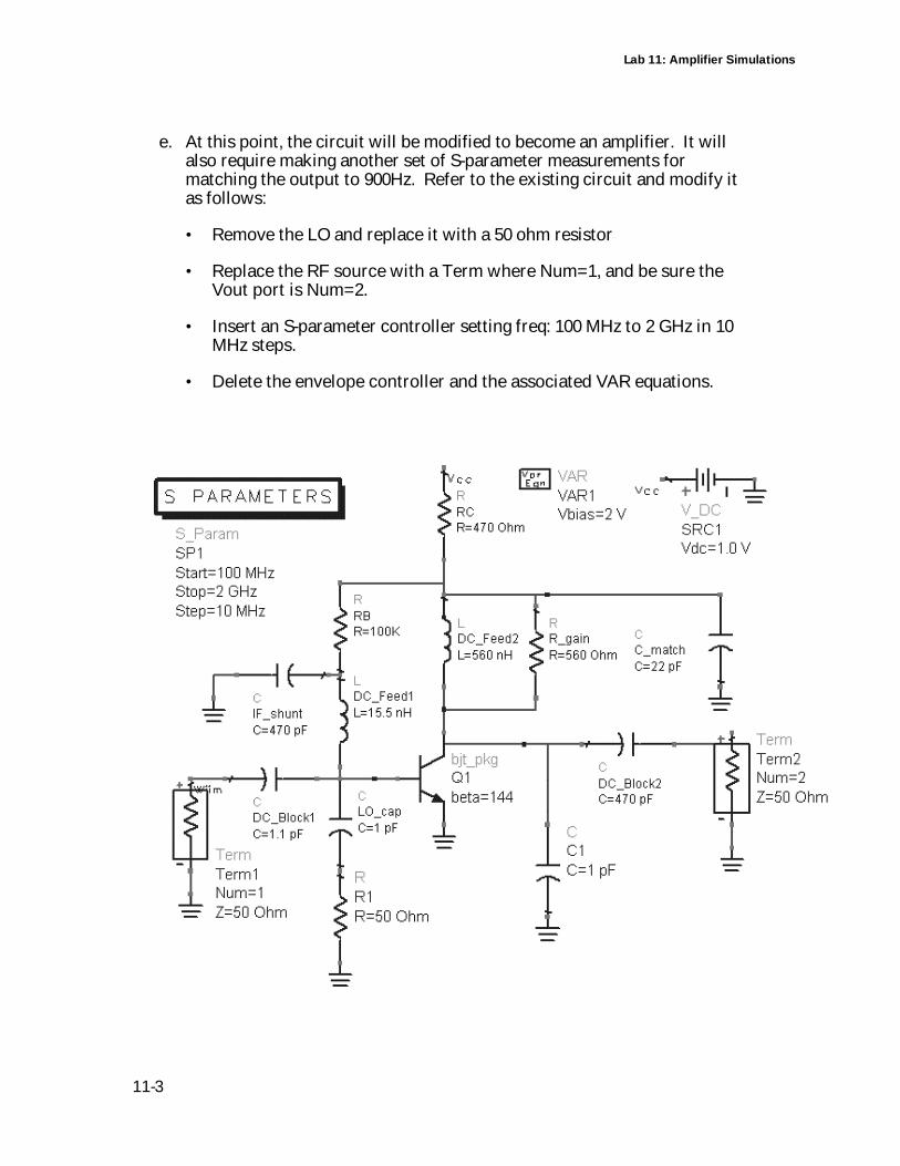
Lab 11: Amplifier Simulations
11-3
e. At this point, the circuit will be modified to become an amplifier. It willalso require making another set of S-parameter measurements formatching the output to 900Hz. Refer to the existing circuit and modify itas follows:
• Remove the LO and replace it with a 50 ohm resistor
• Replace the RF source with a Term where Num=1, and be sure theVout port is Num=2.
• Insert an S-parameter controller setting freq: 100 MHz to 2 GHz in 10MHz steps.
• Delete the envelope controller and the associated VAR equations.
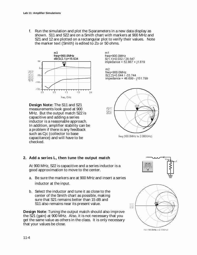
Lab 11: Amplifier Simulations
11-4
f. Run the simulation and plot the S-parameters in a new data display asshown. S11 and S22 are on a Smith chart with markers at 900 MHz andS21 and 12 are plotted on a rectangular plot to verify their values. Notethe marker text (Smith) is edited to Zo or 50 ohms.
Design Note: The S11 and S21measurements look good at 900MHz. But the output match S22 iscapacitive and adding a seriesinductor is a reasonable approach.In addition, amplifier stability can bea problem if there is any feedbacksuch as Cjc (collector to basecapacitance) and will have to bechecked.
2. Add a series L, then tune the output match
At 900 MHz, S22 is capacitive and a series inductor is agood approximation to move to the center.
a. Be sure the markers are at 900 MHz and insert a series
inductor at the input.
b. Select the inductor and tune it as close to thecenter of the Smith chart as possible, makingsure that S21 remains better than 15 dB andS11 also remains near its present value.
Design Note: Tuning the output match should also improvethe S21 (gain) at 900 MHz. Also, it is not necessary that youget the same value as others in the class. It is only necessarythat your values be close.
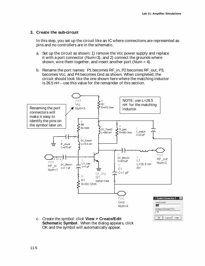
Lab 11: Amplifier Simulations
11-5
3. Create the sub-circuit
In this step, you set up the circuit like an IC where connections are represented aspins and no controllers are in the schematic.
a. Set up the circuit as shown: 1) remove the Vcc power supply and replaceit with a port connector (Num=3), and 2) connect the grounds whereshown, wire them together, and insert another port (Num = 4).
b. Rename the port names: P1 becomes RF_in, P2 becomes RF_out, P3,becomes Vcc, and P4 becomes Gnd as shown. When completed, thecircuit should look like the one shown here where the matching inductoris 26.5 nH – use this value for the remainder of this section.
c. Create the symbol: click View > Create/EditSchematic Symbol. When the dialog appears, clickOK and the symbol will automatically appear.
Renaming the portconnectors willmake it easy toidentify the pins onthe symbol later on.
NOTE: use L=26.5nH for the matchinginductor.
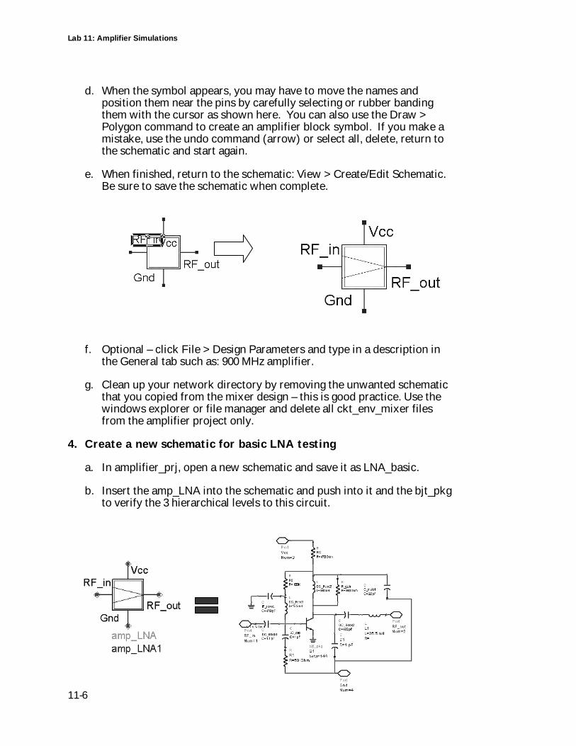
Lab 11: Amplifier Simulations
11-6
d. When the symbol appears, you may have to move the names andposition them near the pins by carefully selecting or rubber bandingthem with the cursor as shown here. You can also use the Draw >Polygon command to create an amplifier block symbol. If you make amistake, use the undo command (arrow) or select all, delete, return tothe schematic and start again.
e. When finished, return to the schematic: View > Create/Edit Schematic.Be sure to save the schematic when complete.
f. Optional – click File > Design Parameters and type in a description inthe General tab such as: 900 MHz amplifier.
g. Clean up your network directory by removing the unwanted schematicthat you copied from the mixer design – this is good practice. Use thewindows explorer or file manager and delete all ckt_env_mixer filesfrom the amplifier project only.
4. Create a new schematic for basic LNA testing
a. In amplifier_prj, open a new schematic and save it as LNA_basic.
b. Insert the amp_LNA into the schematic and push into it and the bjt_pkgto verify the 3 hierarchical levels to this circuit.
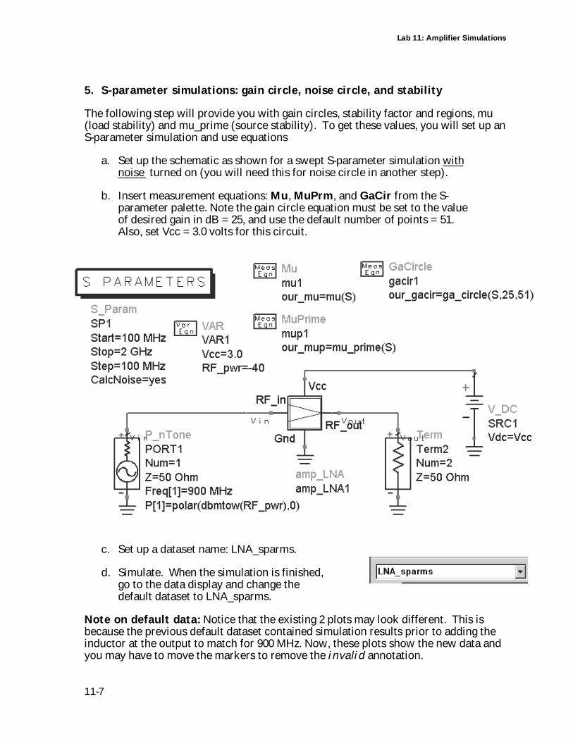
Lab 11: Amplifier Simulations
11-7
5. S-parameter simulations: gain circle, noise circle, and stability
The following step will provide you with gain circles, stability factor and regions, mu(load stability) and mu_prime (source stability). To get these values, you will set up anS-parameter simulation and use equations
a. Set up the schematic as shown for a swept S-parameter simulation withnoise turned on (you will need this for noise circle in another step).
b. Insert measurement equations: Mu, MuPrm, and GaCir from the S-parameter palette. Note the gain circle equation must be set to the valueof desired gain in dB = 25, and use the default number of points = 51.Also, set Vcc = 3.0 volts for this circuit.
c. Set up a dataset name: LNA_sparms.
d. Simulate. When the simulation is finished,go to the data display and change thedefault dataset to LNA_sparms.
Note on default data: Notice that the existing 2 plots may look different. This isbecause the previous default dataset contained simulation results prior to adding theinductor at the output to match for 900 MHz. Now, these plots show the new data andyou may have to move the markers to remove the invalid annotation.
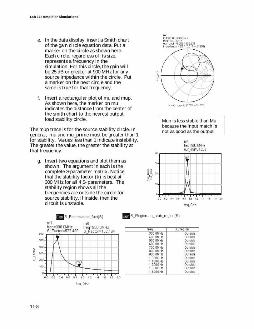
Lab 11: Amplifier Simulations
11-8
e. In the data display, insert a Smith chartof the gain circle equation data. Put amarker on the circle as shown here.Each circle, regardless of its size,represents a frequency in thesimulation. For this circle, the gain willbe 25 dB or greater at 900 MHz for anysource impedance within the circle. Puta marker on the next circle and thesame is true for that frequency.
f. Insert a rectangular plot of mu and mup.As shown here, the marker on muindicates the distance from the center ofthe smith chart to the nearest outputload stability circle.
The mup trace is for the source stability circle. Ingeneral, mu and mu_prime must be greater than 1for stability. Values less than 1 indicate instability.The greater the value, the greater the stability atthat frequency.
g. Insert two equations and plot them asshown. The argument in each is thecomplete S-parameter matrix. Noticethat the stability factor (k) is best at300 MHz for all 4 S- parameters. Thestability region shows all thefrequencies are outside the circle forsource stability. If inside, then thecircuit is unstable.
Mup is less stable than Mubecause the input match isnot as good as the output
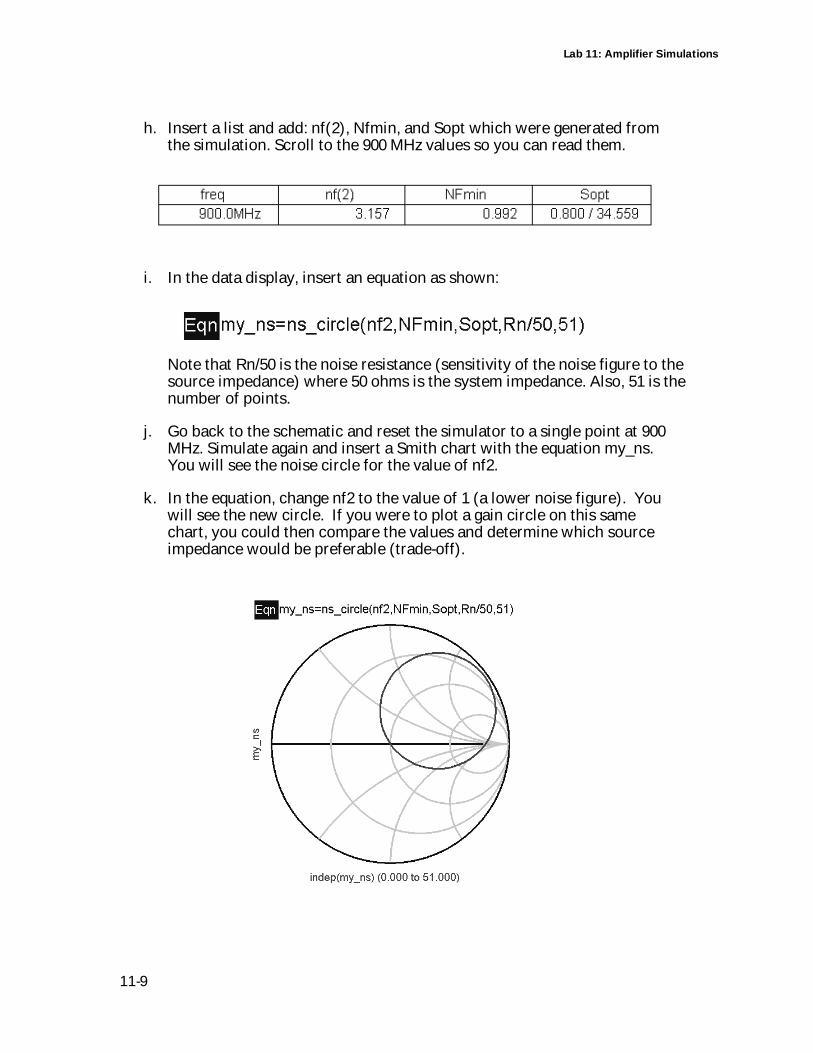
Lab 11: Amplifier Simulations
11-9
h. Insert a list and add: nf(2), Nfmin, and Sopt which were generated fromthe simulation. Scroll to the 900 MHz values so you can read them.
i. In the data display, insert an equation as shown:
Note that Rn/50 is the noise resistance (sensitivity of the noise figure to thesource impedance) where 50 ohms is the system impedance. Also, 51 is thenumber of points.
j. Go back to the schematic and reset the simulator to a single point at 900MHz. Simulate again and insert a Smith chart with the equation my_ns.You will see the noise circle for the value of nf2.
k. In the equation, change nf2 to the value of 1 (a lower noise figure). Youwill see the new circle. If you were to plot a gain circle on this samechart, you could then compare the values and determine which sourceimpedance would be preferable (trade-off).
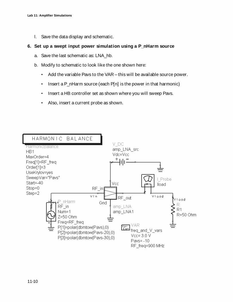
Lab 11: Amplifier Simulations
11-10
l. Save the data display and schematic.
6. Set up a swept input power simulation using a P_nHarm source
a. Save the last schematic as: LNA_hb.
b. Modify to schematic to look like the one shown here:
• Add the variable Pavs to the VAR – this will be available source power.
• Insert a P_nHarm source (each P[n] is the power in that harmonic)
• Insert a HB controller set as shown where you will sweep Pavs.
• Also, insert a current probe as shown.
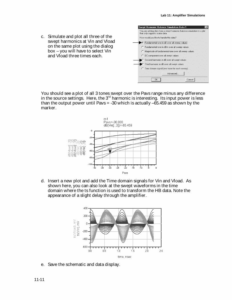
Lab 11: Amplifier Simulations
11-11
c. Simulate and plot all three of theswept harmonics at Vin and Vloadon the same plot using the dialogbox – you will have to select Vinand Vload three times each.
You should see a plot of all 3 tones swept over the Pavs range minus any differencein the source settings. Here, the 3rd harmonic is interesting. Its input power is lessthan the output power until Pavs = -30 which is actually –65.459 as shown by themarker.
d. Insert a new plot and add the Time domain signals for Vin and Vload. Asshown here, you can also look at the swept waveforms in the timedomain where the ts function is used to transform the HB data. Note theappearance of a slight delay through the amplifier.
e. Save the schematic and data display.
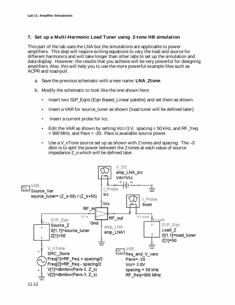
Lab 11: Amplifier Simulations
11-12
7. Set up a Multi-Harmonic Load Tuner using 2-tone HB simulation
This part of the lab uses the LNA but the simulations are applicable to poweramplifiers. This step will require writing equations to vary the load and source fordifferent harmonics and will take longer than other labs to set up the simulation anddata display. However, the results that you achieve will be very powerful for designingamplifiers. Also, this will help you to use the more powerful example files such asACPR and load-pull.
a. Save the previous schematic with a new name: LNA_2tone.
b. Modify the schematic to look like the one shown here:
• Insert two S1P_Eqns (Eqn Based_Linear palette) and set them as shown.
• Insert a VAR for source_tuner as shown (load tuner will be defined later).
• Insert a current probe for Icc.
• Edit the VAR as shown by setting Vcc=3 V, spacing = 50 kHz, and RF_freq= 900 MHz, and Pavs = -20. Pavs is available source power.
• Use a V_nTone source set up as shown with 2 tones and spacing. The –3dbm is to split the power between the 2 tones at each value of sourceimpedance Z_s which will be defined later.
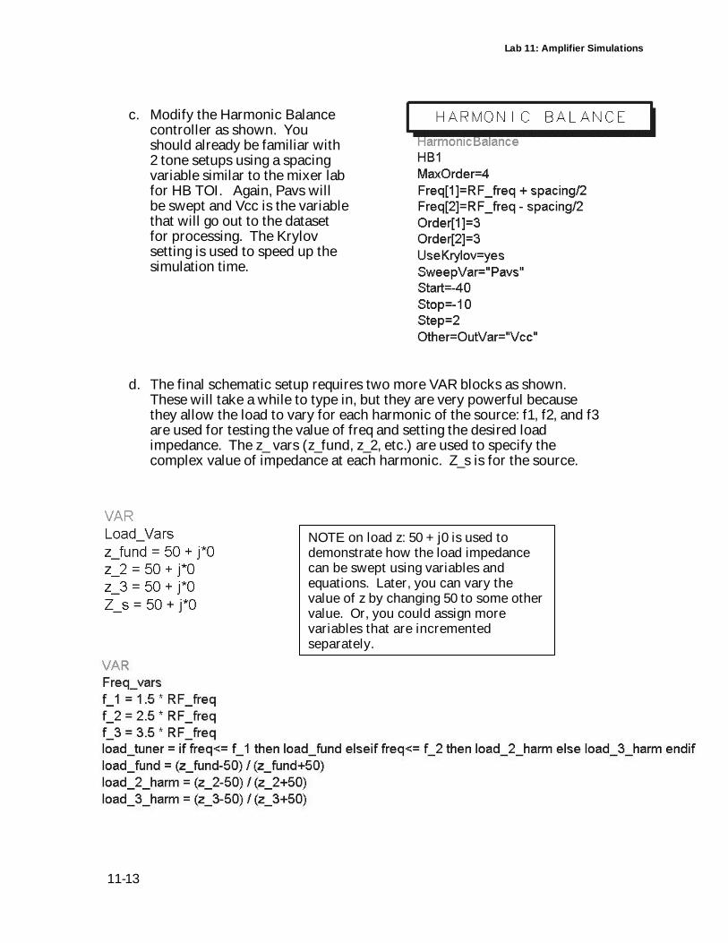
Lab 11: Amplifier Simulations
11-13
c. Modify the Harmonic Balancecontroller as shown. Youshould already be familiar with2 tone setups using a spacingvariable similar to the mixer labfor HB TOI. Again, Pavs willbe swept and Vcc is the variablethat will go out to the datasetfor processing. The Krylovsetting is used to speed up thesimulation time.
d. The final schematic setup requires two more VAR blocks as shown.These will take a while to type in, but they are very powerful becausethey allow the load to vary for each harmonic of the source: f1, f2, and f3are used for testing the value of freq and setting the desired loadimpedance. The z_ vars (z_fund, z_2, etc.) are used to specify thecomplex value of impedance at each harmonic. Z_s is for the source.
NOTE on load z: 50 + j0 is used todemonstrate how the load impedancecan be swept using variables andequations. Later, you can vary thevalue of z by changing 50 to some othervalue. Or, you could assign morevariables that are incrementedseparately.
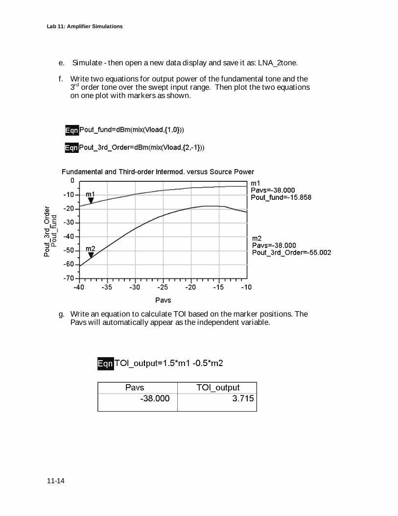
Lab 11: Amplifier Simulations
11-14
e. Simulate - then open a new data display and save it as: LNA_2tone.
f. Write two equations for output power of the fundamental tone and the3rd order tone over the swept input range. Then plot the two equationson one plot with markers as shown.
g. Write an equation to calculate TOI based on the marker positions. ThePavs will automatically appear as the independent variable.
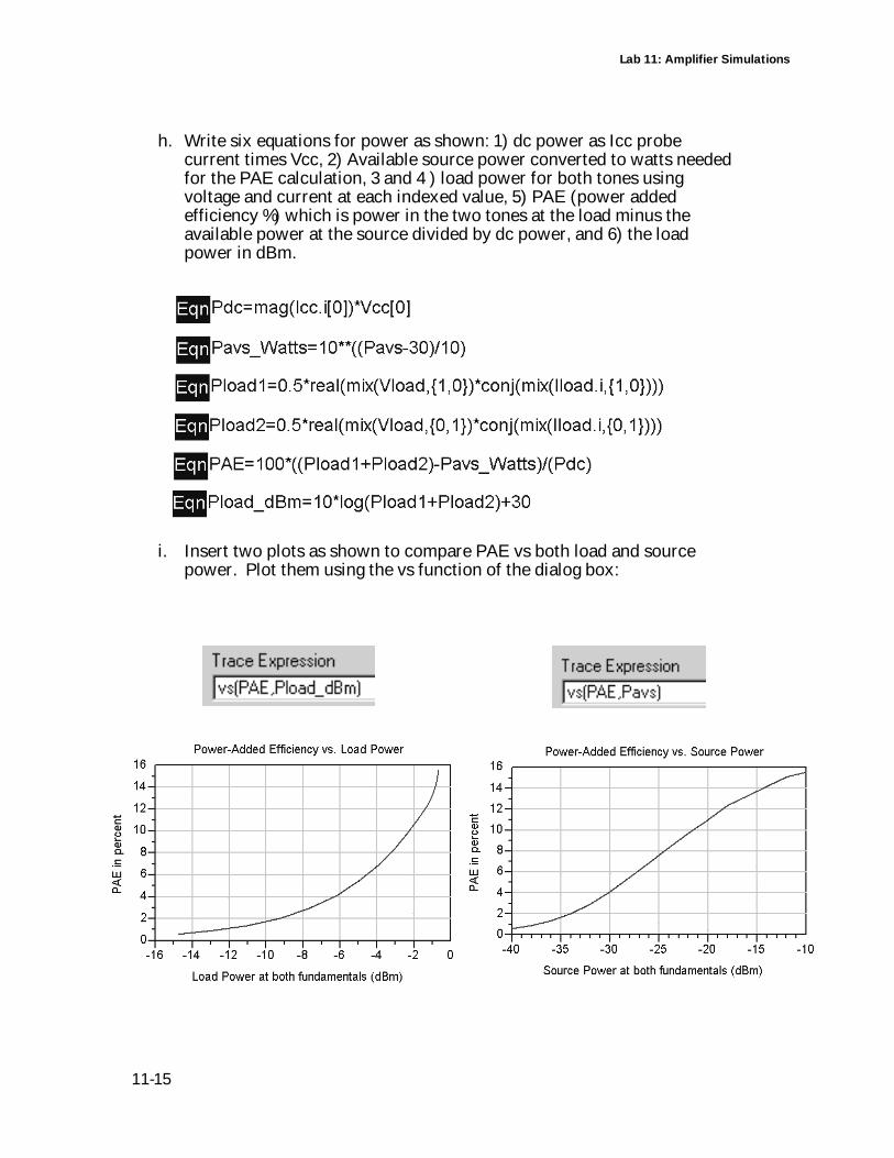
Lab 11: Amplifier Simulations
11-15
h. Write six equations for power as shown: 1) dc power as Icc probecurrent times Vcc, 2) Available source power converted to watts neededfor the PAE calculation, 3 and 4 ) load power for both tones usingvoltage and current at each indexed value, 5) PAE (power addedefficiency %) which is power in the two tones at the load minus theavailable power at the source divided by dc power, and 6) the loadpower in dBm.
i. Insert two plots as shown to compare PAE vs both load and sourcepower. Plot them using the vs function of the dialog box:
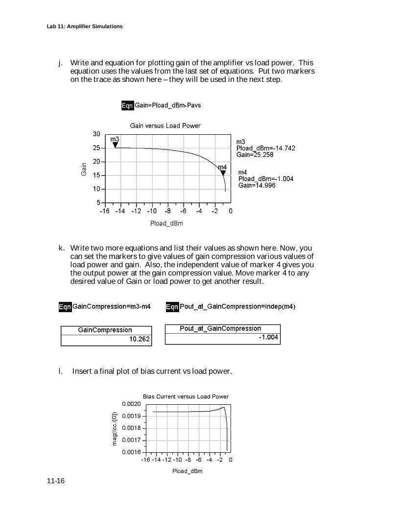
Lab 11: Amplifier Simulations
11-16
j. Write and equation for plotting gain of the amplifier vs load power. Thisequation uses the values from the last set of equations. Put two markerson the trace as shown here – they will be used in the next step.
k. Write two more equations and list their values as shown here. Now, youcan set the markers to give values of gain compression various values ofload power and gain. Also, the independent value of marker 4 gives youthe output power at the gain compression value. Move marker 4 to anydesired value of Gain or load power to get another result.
l. Insert a final plot of bias current vs load power.
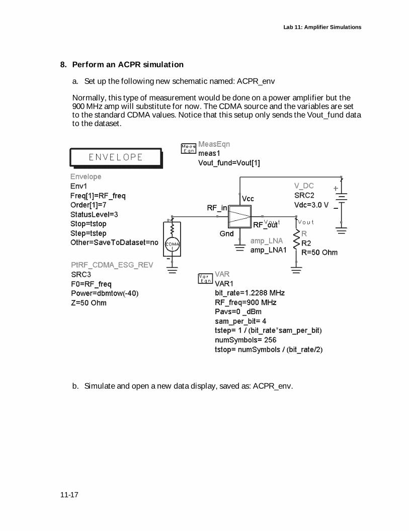
Lab 11: Amplifier Simulations
11-17
8. Perform an ACPR simulation
a. Set up the following new schematic named: ACPR_env
Normally, this type of measurement would be done on a power amplifier but the900 MHz amp will substitute for now. The CDMA source and the variables are setto the standard CDMA values. Notice that this setup only sends the Vout_fund datato the dataset.
b. Simulate and open a new data display, saved as: ACPR_env.
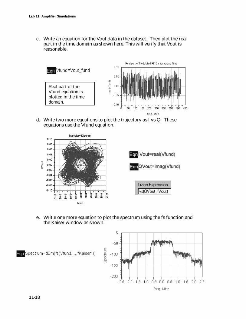
Lab 11: Amplifier Simulations
11-18
c. Write an equation for the Vout data in the dataset. Then plot the realpart in the time domain as shown here. This will verify that Vout isreasonable.
d. Write two more equations to plot the trajectory as I vs Q. Theseequations use the Vfund equation.
e. Writ e one more equation to plot the spectrum using the fs function andthe Kaiser window as shown.
Real part of theVfund equation isplotted in the timedomain.
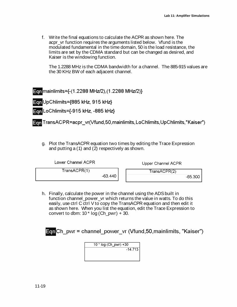
Lab 11: Amplifier Simulations
11-19
f. Write the final equations to calculate the ACPR as shown here. Theacpr_vr function requires the arguments listed below. Vfund is themodulated fundamental in the time domain, 50 is the load resistance, thelimits are set by the CDMA standard but can be changed as desired, andKaiser is the windowing function.
The 1.2288 MHz is the CDMA bandwidth for a channel. The 885-915 values arethe 30 KHz BW of each adjacent channel.
g. Plot the TransACPR equation two times by editing the Trace Expressionand putting a (1) and (2) respectively as shown.
h. Finally, calculate the power in the channel using the ADS built infunction channel_power_vr which returns the value in watts. To do thiseasily, use ctrl C ctrl V to copy the TransACPR equation and then edit itas shown here. When you list the equation, edit the Trace Expression toconvert to dbm: 10 * log (Ch_pwr) + 30.
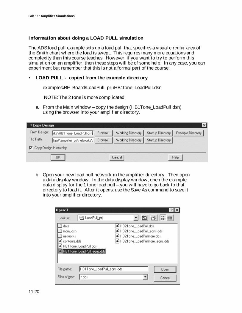
Lab 11: Amplifier Simulations
11-20
Information about doing a LOAD PULL simulation
The ADS load pull example sets up a load pull that specifies a visual circular area ofthe Smith chart where the load is swept. This requires many more equations andcomplexity than this course teaches. However, if you want to try to perform thissimulation on an amplifier, then these steps will be of some help. In any case, you canexperiment but remember that this is not a formal part of the course:
• LOAD PULL - copied from the example directory
examples\RF_Board\LoadPull_prj\HB1tone_LoadPull.dsn
NOTE: The 2 tone is more complicated.
a. From the Main window – copy the design (HB1Tone_LoadPull.dsn)using the browser into your amplifier directory.
b. Open your new load pull network in the amplifier directory. Then opena data display window. In the data display window, open the exampledata display for the 1 tone load pull – you will have to go back to thatdirectory to load it. After it opens, use the Save As command to save itinto your amplifier directory.
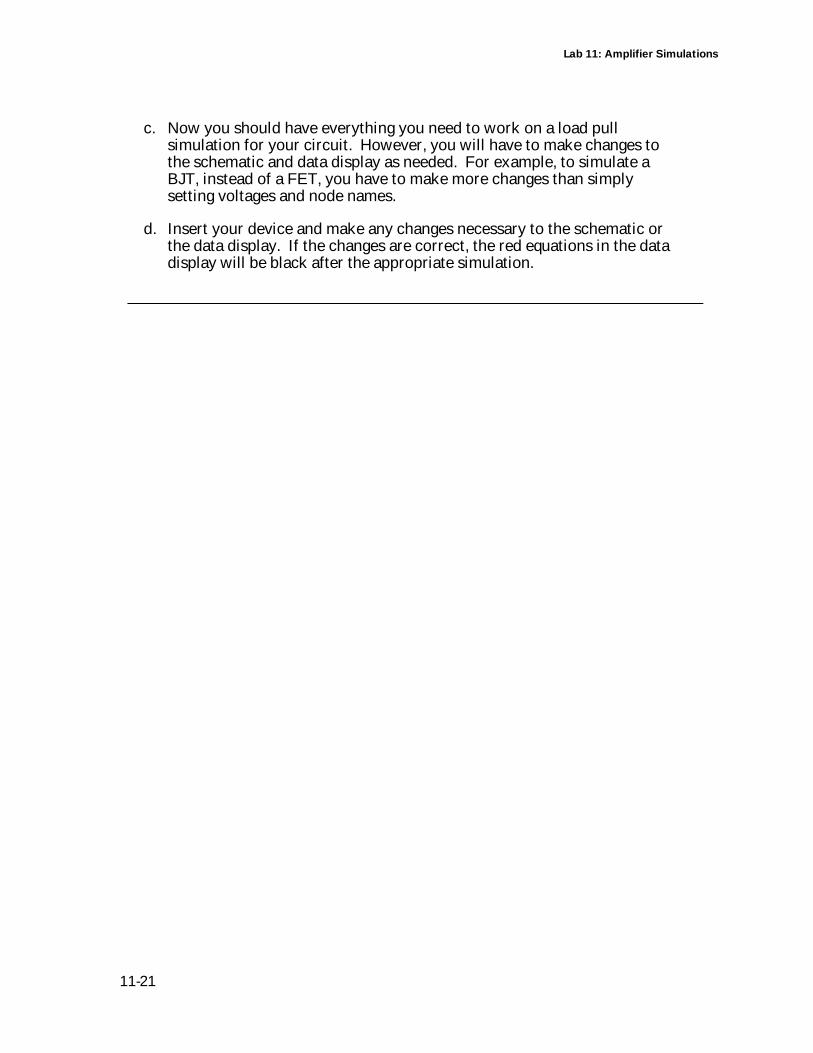
Lab 11: Amplifier Simulations
11-21
c. Now you should have everything you need to work on a load pullsimulation for your circuit. However, you will have to make changes tothe schematic and data display as needed. For example, to simulate aBJT, instead of a FET, you have to make more changes than simplysetting voltages and node names.
d. Insert your device and make any changes necessary to the schematic orthe data display. If the changes are correct, the red equations in the datadisplay will be black after the appropriate simulation.
________________________________________________________________________
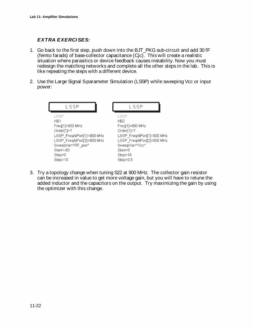
Lab 11: Amplifier Simulations
11-22
EXTRA EXERCISES:
1. Go back to the first step, push down into the BJT_PKG sub-circuit and add 30 fF(femto farads) of base-collector capacitance (Cjc). This will create a realisticsituation where parasitics or device feedback causes instability. Now you mustredesign the matching networks and complete all the other steps in the lab. This islike repeating the steps with a different device.
2. Use the Large Signal S-parameter Simulation (LSSP) while sweeping Vcc or inputpower:
3. Try a topology change when tuning S22 at 900 MHz. The collector gain resistorcan be increased in value to get more voltage gain, but you will have to retune theadded inductor and the capacitors on the output. Try maximizing the gain by usingthe optimizer with this change.
12
This chapter shows the basics of simulating oscillators todetermine several basic specifications.
Lab 12: Oscillator Simulations
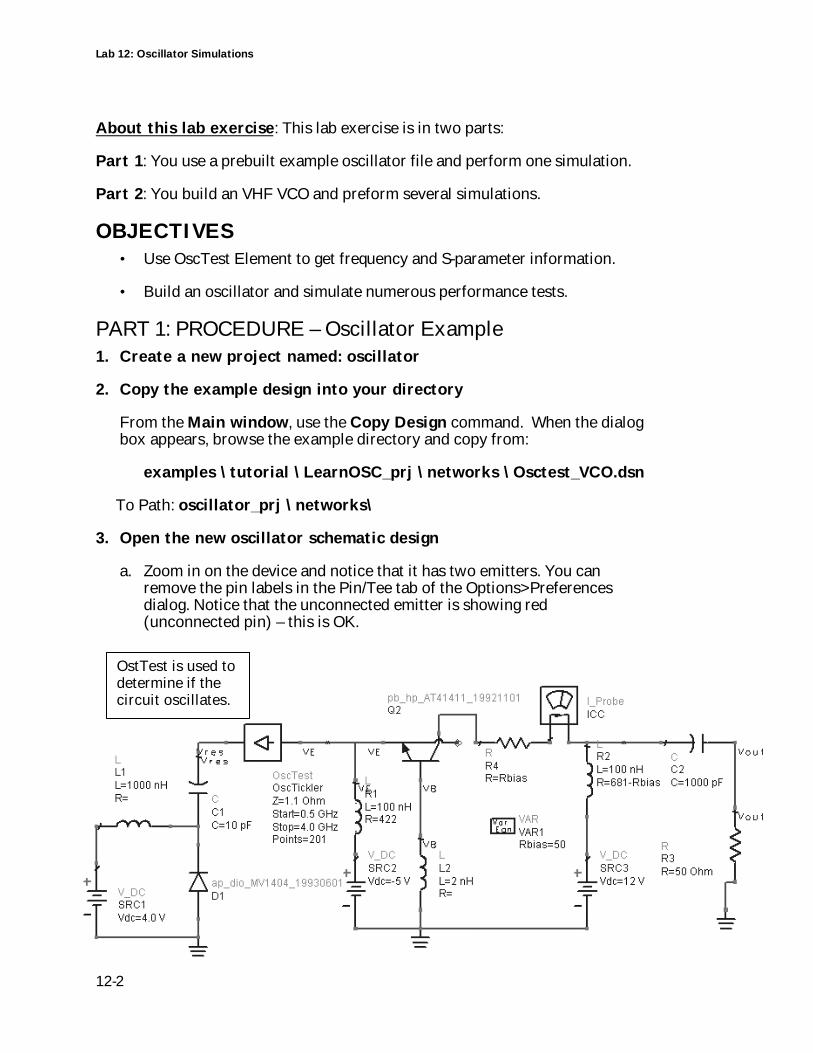
Lab 12: Oscillator Simulations
12-2
About this lab exercise: This lab exercise is in two parts:
Part 1: You use a prebuilt example oscillator file and perform one simulation.
Part 2: You build an VHF VCO and preform several simulations.
OBJECTIVES• Use OscTest Element to get frequency and S-parameter information.
• Build an oscillator and simulate numerous performance tests.
PART 1: PROCEDURE – Oscillator Example1. Create a new project named: oscillator
2. Copy the example design into your directory
From the Main window, use the Copy Design command. When the dialogbox appears, browse the example directory and copy from:
examples \ tutorial \ LearnOSC_prj \ networks \ Osctest_VCO.dsn
To Path: oscillator_prj \ networks\
3. Open the new oscillator schematic design
a. Zoom in on the device and notice that it has two emitters. You canremove the pin labels in the Pin/Tee tab of the Options>Preferencesdialog. Notice that the unconnected emitter is showing red(unconnected pin) – this is OK.
OstTest is used todetermine if thecircuit oscillates.
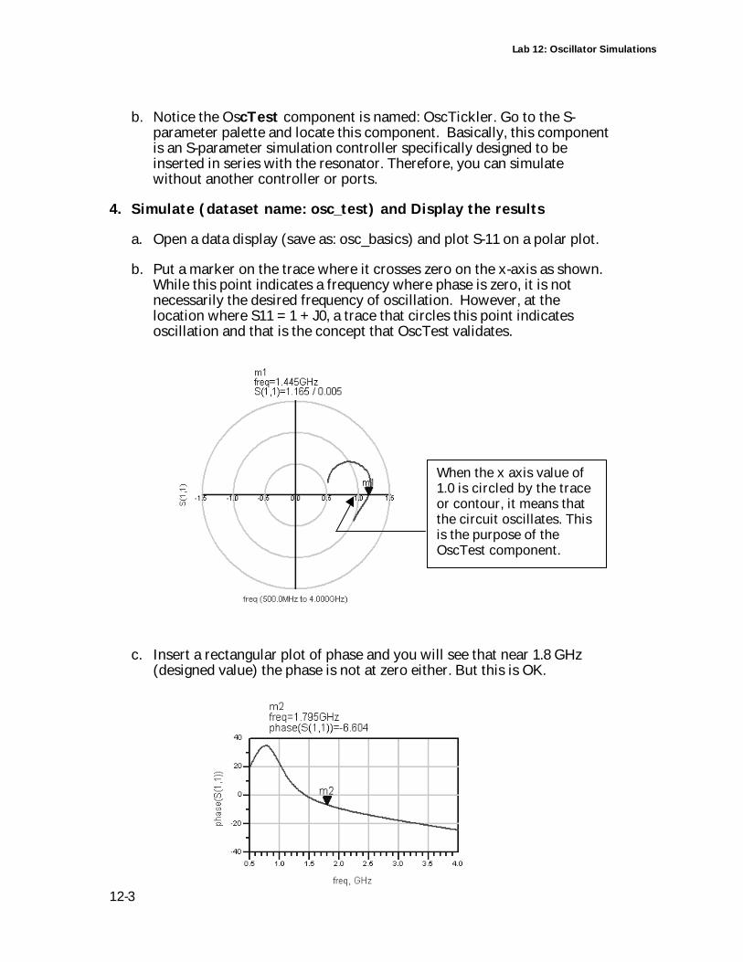
Lab 12: Oscillator Simulations
12-3
b. Notice the OscTest component is named: OscTickler. Go to the S-parameter palette and locate this component. Basically, this componentis an S-parameter simulation controller specifically designed to beinserted in series with the resonator. Therefore, you can simulatewithout another controller or ports.
4. Simulate (dataset name: osc_test) and Display the results
a. Open a data display (save as: osc_basics) and plot S-11 on a polar plot.
b. Put a marker on the trace where it crosses zero on the x-axis as shown.While this point indicates a frequency where phase is zero, it is notnecessarily the desired frequency of oscillation. However, at thelocation where S11 = 1 + J0, a trace that circles this point indicatesoscillation and that is the concept that OscTest validates.
c. Insert a rectangular plot of phase and you will see that near 1.8 GHz(designed value) the phase is not at zero either. But this is OK.
When the x axis value of1.0 is circled by the traceor contour, it means thatthe circuit oscillates. Thisis the purpose of theOscTest component.
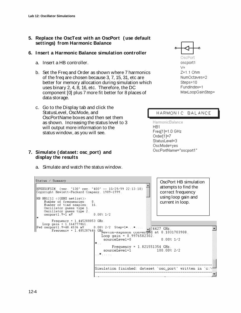
Lab 12: Oscillator Simulations
12-4
5. Replace the OscTest with an OscPort (use defaultsettings) from Harmonic Balance
6. Insert a Harmonic Balance simulation controller
a. Insert a HB controller.
b. Set the Freq and Order as shown where 7 harmonicsof the freq are chosen because 3, 7, 15, 31, etc arebetter for memory allocation during simulation whichuses binary 2, 4, 8, 16, etc. Therefore, the DCcomponent [0] plus 7 more fit better for 8 places ofdata storage.
c. Go to the Display tab and click theStatusLevel, OscMode, andOscPortName boxes and then set themas shown. Increasing the status level to 3will output more information to thestatus window, as you will see.
7. Simulate (dataset: osc_port) anddisplay the results
a. Simulate and watch the status window.
OscPort HB simulationattempts to find thecorrect frequencyusing loop gain andcurrent in loop.
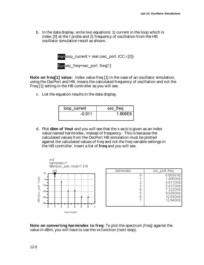
Lab 12: Oscillator Simulations
12-5
b. In the data display, write two equations: 1) current in the loop which isindex [0] at the I probe and 2) frequency of oscillation from the HBoscillator simulation result as shown.
Note on freq[1] value: Index value freq [1] in the case of an oscillator simulation,using the OscPort and HB, means the calculated frequency of oscillation and not theFreq [1] setting in the HB controller as you will see.
c. List the equation results in the data display.
d. Plot dbm of Vout and you will see that the x-axis is given as an indexvalue named harmindex, instead of frequency. This is because thecalculated values from the OscPort HB simulation must be plottedagainst the calculated values of freq and not the freq variable settings inthe HB controller. Insert a list of freq and you will see.
Note on converting harmindex to freq: To plot the spectrum (freq) against thevalue in dBm, you will have to use the vs function (next step).
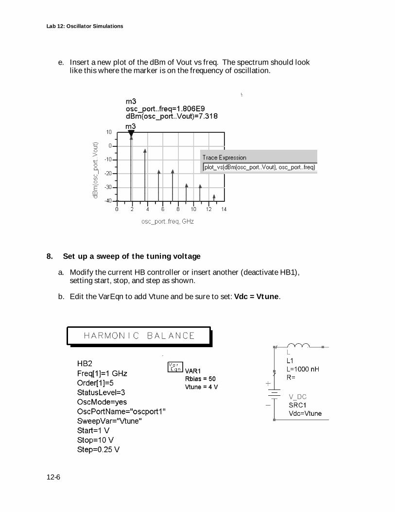
Lab 12: Oscillator Simulations
12-6
e. Insert a new plot of the dBm of Vout vs freq. The spectrum should looklike this where the marker is on the frequency of oscillation.
8. Set up a sweep of the tuning voltage
a. Modify the current HB controller or insert another (deactivate HB1),setting start, stop, and step as shown.
b. Edit the VarEqn to add Vtune and be sure to set: Vdc = Vtune.
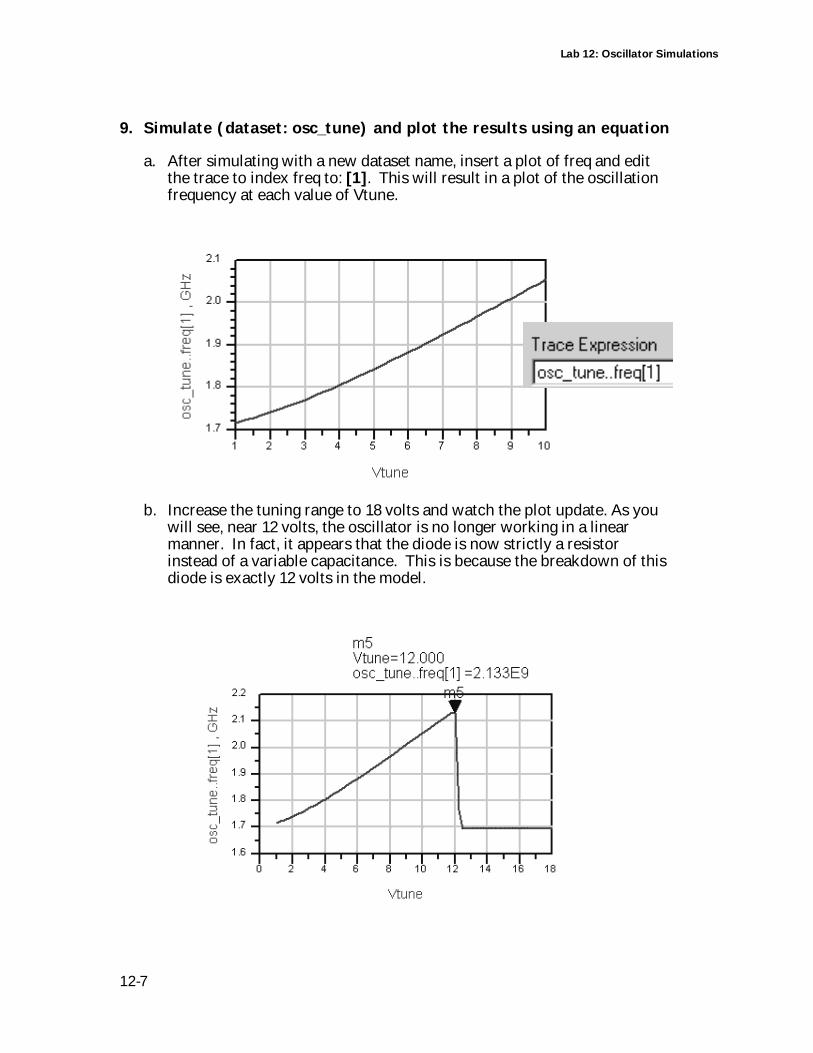
Lab 12: Oscillator Simulations
12-7
9. Simulate (dataset: osc_tune) and plot the results using an equation
a. After simulating with a new dataset name, insert a plot of freq and editthe trace to index freq to: [1]. This will result in a plot of the oscillationfrequency at each value of Vtune.
b. Increase the tuning range to 18 volts and watch the plot update. As youwill see, near 12 volts, the oscillator is no longer working in a linearmanner. In fact, it appears that the diode is now strictly a resistorinstead of a variable capacitance. This is because the breakdown of thisdiode is exactly 12 volts in the model.
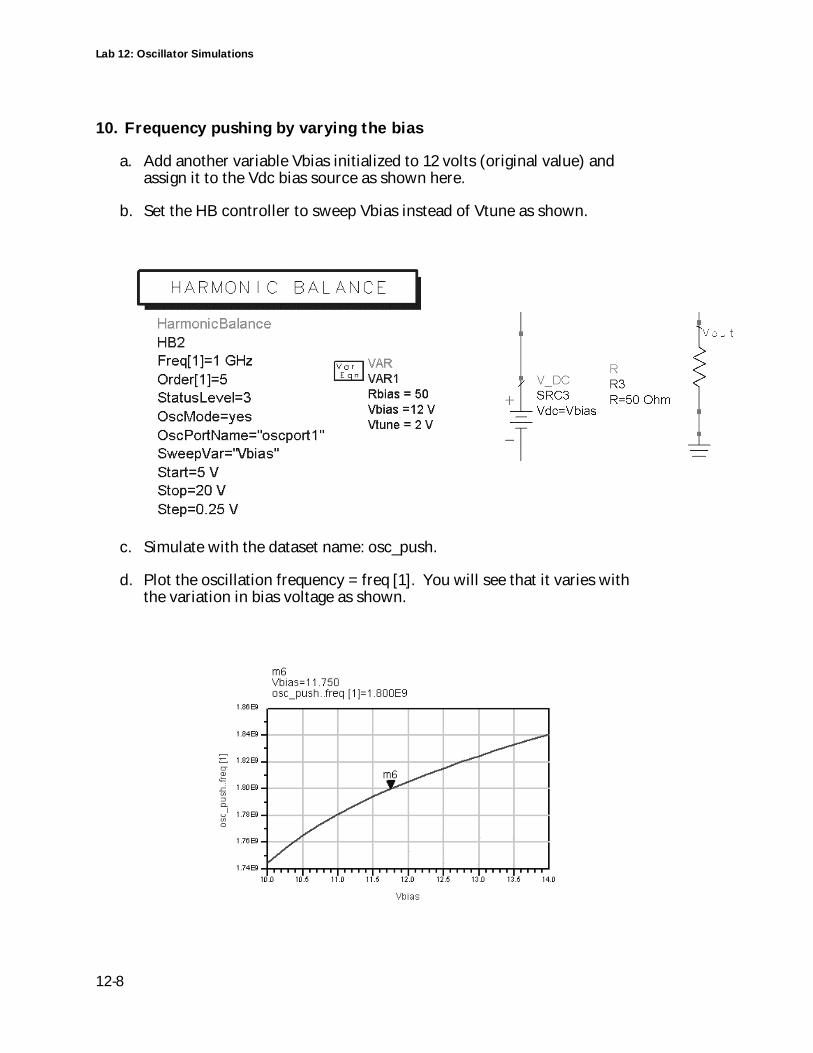
Lab 12: Oscillator Simulations
12-8
10. Frequency pushing by varying the bias
a. Add another variable Vbias initialized to 12 volts (original value) andassign it to the Vdc bias source as shown here.
b. Set the HB controller to sweep Vbias instead of Vtune as shown.
c. Simulate with the dataset name: osc_push.
d. Plot the oscillation frequency = freq [1]. You will see that it varies withthe variation in bias voltage as shown.
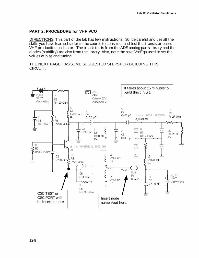
Lab 12: Oscillator Simulations
12-9
PART 2: PROCEDURE for VHF VCO
DIRECTIONS: This part of the lab has few instructions. So, be careful and use all theskills you have learned so far in the course to construct and test this transistor-basedVHF production oscillator. The transistor is from the ADS analog parts library and thediodes (stability) are also from the library. Also, note the save VarEqn used to set thevalues of bias and tuning.
THE NEXT PAGE HAS SOME SUGGESTED STEPS FOR BUILDING THISCIRCUIT.
Insert nodename Vout here.
OSC TEST orOSC PORT willbe inserted here.
It takes about 15 minutes tobuild this circuit.
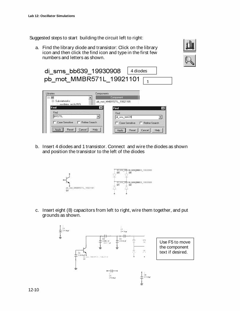
Lab 12: Oscillator Simulations
12-10
Suggested steps to start building the circuit left to right:
a. Find the library diode and transistor: Click on the libraryicon and then click the find icon and type in the first fewnumbers and letters as shown.
b. Insert 4 diodes and 1 transistor. Connect and wire the diodes as shownand position the transistor to the left of the diodes
c. Insert eight (8) capacitors from left to right, wire them together, and putgrounds as shown.
4 diodes
1
Use F5 to movethe componenttext if desired.
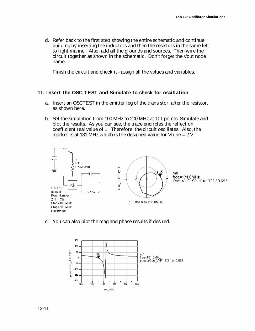
Lab 12: Oscillator Simulations
12-11
d. Refer back to the first step showing the entire schematic and continuebuilding by inserting the inductors and then the resistors in the same leftto right manner. Also, add all the grounds and sources. Then wire thecircuit together as shown in the schematic. Don’t forget the Vout nodename.
Finish the circuit and check it - assign all the values and variables.
11. Insert the OSC TEST and Simulate to check for oscillation
a. Insert an OSCTEST in the emitter leg of the transistor, after the resistor,as shown here.
b. Set the simulation from 100 MHz to 200 MHz at 101 points. Simulate andplot the results. As you can see, the trace encircles the reflectioncoefficient real value of 1. Therefore, the circuit oscillates. Also, themarker is at 131 MHz which is the designed value for Vtune = 2 V.
c. You can also plot the mag and phase results if desired.
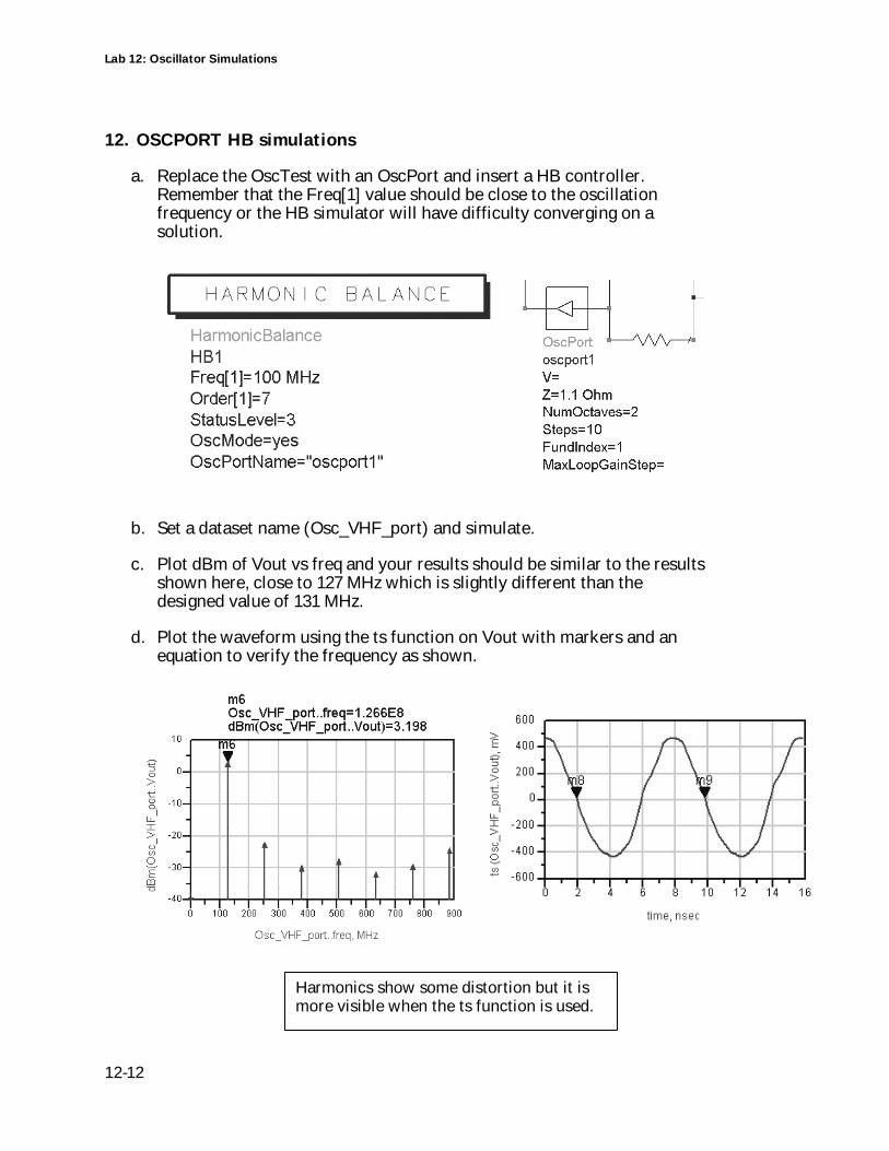
Lab 12: Oscillator Simulations
12-12
12. OSCPORT HB simulations
a. Replace the OscTest with an OscPort and insert a HB controller.Remember that the Freq[1] value should be close to the oscillationfrequency or the HB simulator will have difficulty converging on asolution.
b. Set a dataset name (Osc_VHF_port) and simulate.
c. Plot dBm of Vout vs freq and your results should be similar to the resultsshown here, close to 127 MHz which is slightly different than thedesigned value of 131 MHz.
d. Plot the waveform using the ts function on Vout with markers and anequation to verify the frequency as shown.
Harmonics show some distortion but it ismore visible when the ts function is used.
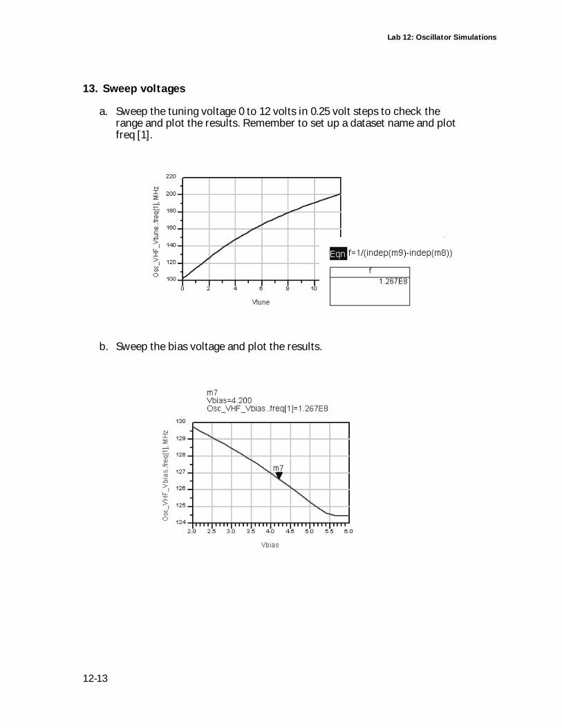
Lab 12: Oscillator Simulations
12-13
13. Sweep voltages
a. Sweep the tuning voltage 0 to 12 volts in 0.25 volt steps to check therange and plot the results. Remember to set up a dataset name and plotfreq [1].
b. Sweep the bias voltage and plot the results.
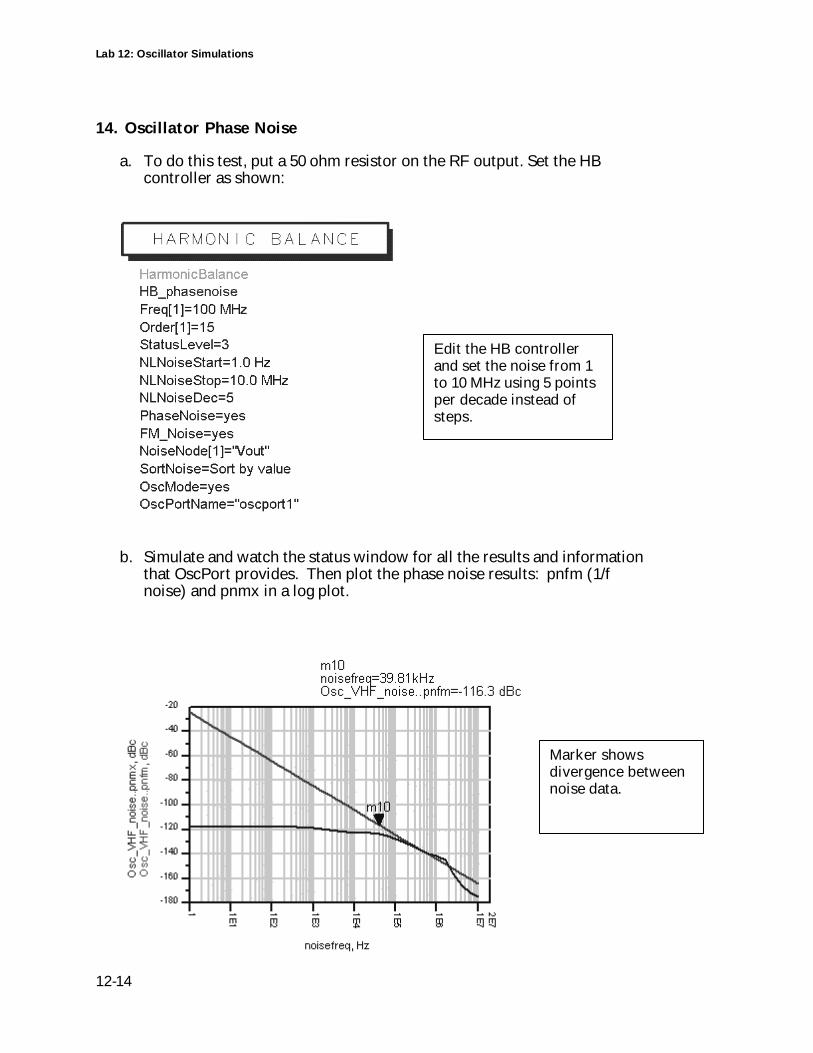
Lab 12: Oscillator Simulations
12-14
14. Oscillator Phase Noise
a. To do this test, put a 50 ohm resistor on the RF output. Set the HBcontroller as shown:
b. Simulate and watch the status window for all the results and informationthat OscPort provides. Then plot the phase noise results: pnfm (1/fnoise) and pnmx in a log plot.
Marker showsdivergence betweennoise data.
Edit the HB controllerand set the noise from 1to 10 MHz using 5 pointsper decade instead ofsteps.

Lab 12: Oscillator Simulations
12-15
EXTRA EXERCISES:
1. In Part 2, try putting a 50 ohm resistor on the Vout node and note any differenceswith this load. Then sweep the load and look at the results.
2. In Part 2, try setting the HB controller over sampling to 3 or 4 and also set thenumber of harmonics to 15 and see if the oscillator harmonics or waveformimprove with the simulation.
3. In Part 2, try redesigning the oscillator to have better harmonic roll off.
4. In Part 1, try measuring phase noise.

Lab 12: Oscillator Simulations
12-16
THIS PAGE IS INTENTIONALLY BLANK.
13
This chapter shows the basics of using Layout for creatingphysical designs, for generating layouts from schematics, andsimulating from layout or schematic. It also demonstratesBoolean operations, DRC, and the GCC.
Lab 13: Layout Basics
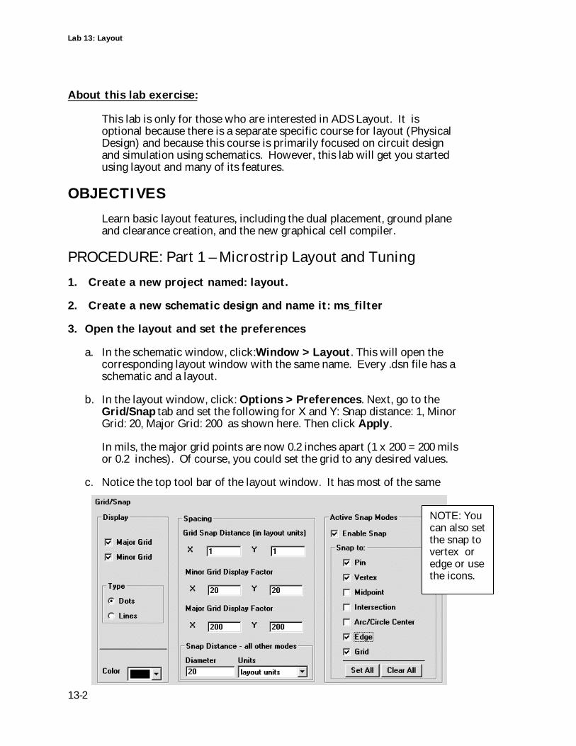
Lab 13: Layout
13-2
About this lab exercise:
This lab is only for those who are interested in ADS Layout. It isoptional because there is a separate specific course for layout (PhysicalDesign) and because this course is primarily focused on circuit designand simulation using schematics. However, this lab will get you startedusing layout and many of its features.
OBJECTIVES
Learn basic layout features, including the dual placement, ground planeand clearance creation, and the new graphical cell compiler.
PROCEDURE: Part 1 – Microstrip Layout and Tuning
1. Create a new project named: layout.
2. Create a new schematic design and name it: ms_filter
3. Open the layout and set the preferences
a. In the schematic window, click:Window > Layout. This will open thecorresponding layout window with the same name. Every .dsn file has aschematic and a layout.
b. In the layout window, click: Options > Preferences. Next, go to theGrid/Snap tab and set the following for X and Y: Snap distance: 1, MinorGrid: 20, Major Grid: 200 as shown here. Then click Apply.
In mils, the major grid points are now 0.2 inches apart (1 x 200 = 200 milsor 0.2 inches). Of course, you could set the grid to any desired values.
c. Notice the top tool bar of the layout window. It has most of the same
NOTE: Youcan also setthe snap tovertex oredge or usethe icons.
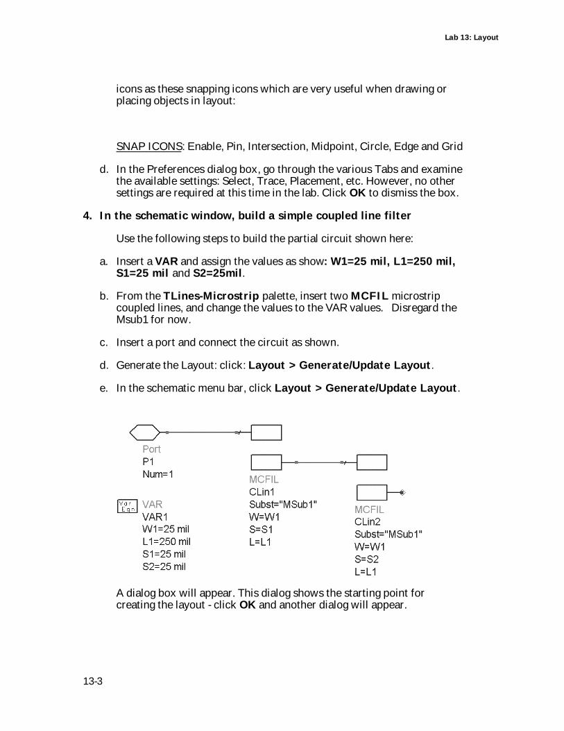
Lab 13: Layout
13-3
icons as these snapping icons which are very useful when drawing orplacing objects in layout:
SNAP ICONS: Enable, Pin, Intersection, Midpoint, Circle, Edge and Grid
d. In the Preferences dialog box, go through the various Tabs and examinethe available settings: Select, Trace, Placement, etc. However, no othersettings are required at this time in the lab. Click OK to dismiss the box.
4. In the schematic window, build a simple coupled line filter
Use the following steps to build the partial circuit shown here:
a. Insert a VAR and assign the values as show: W1=25 mil, L1=250 mil,S1=25 mil and S2=25mil.
b. From the TLines-Microstrip palette, insert two MCFIL microstripcoupled lines, and change the values to the VAR values. Disregard theMsub1 for now.
c. Insert a port and connect the circuit as shown.
d. Generate the Layout: click: Layout > Generate/Update Layout.
e. In the schematic menu bar, click Layout > Generate/Update Layout.
A dialog box will appear. This dialog shows the starting point forcreating the layout - click OK and another dialog will appear.
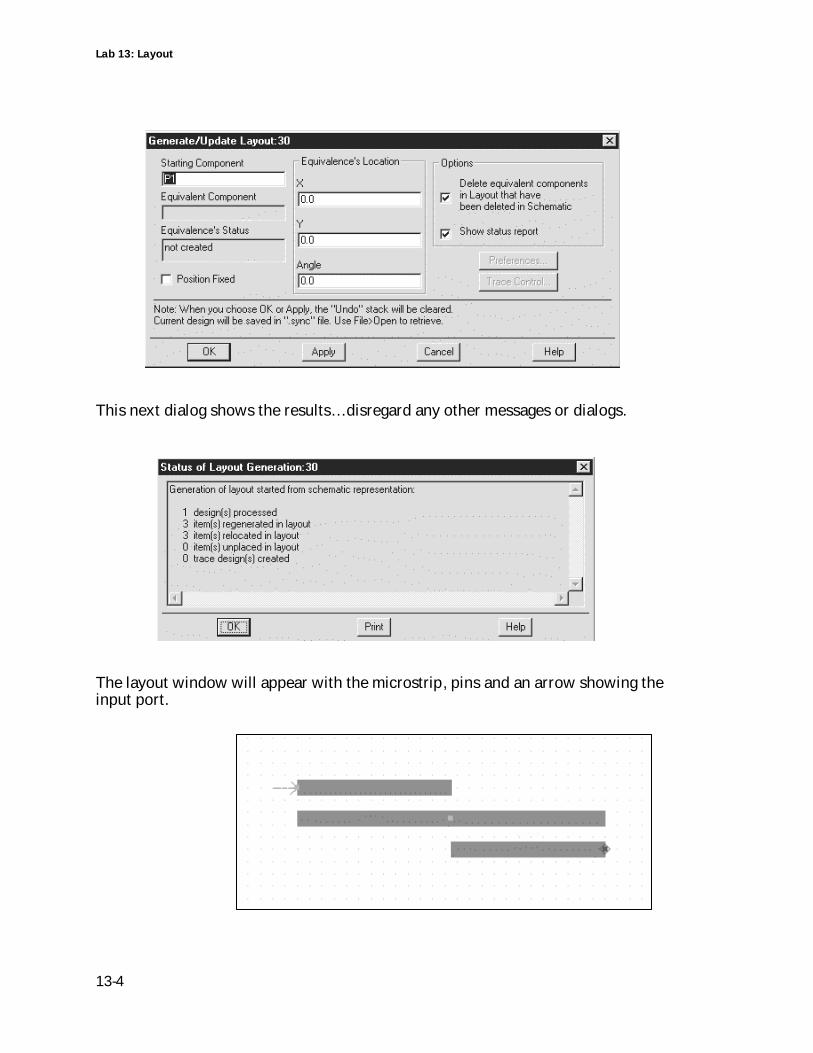
Lab 13: Layout
13-4
This next dialog shows the results…disregard any other messages or dialogs.
The layout window will appear with the microstrip, pins and an arrow showing theinput port.
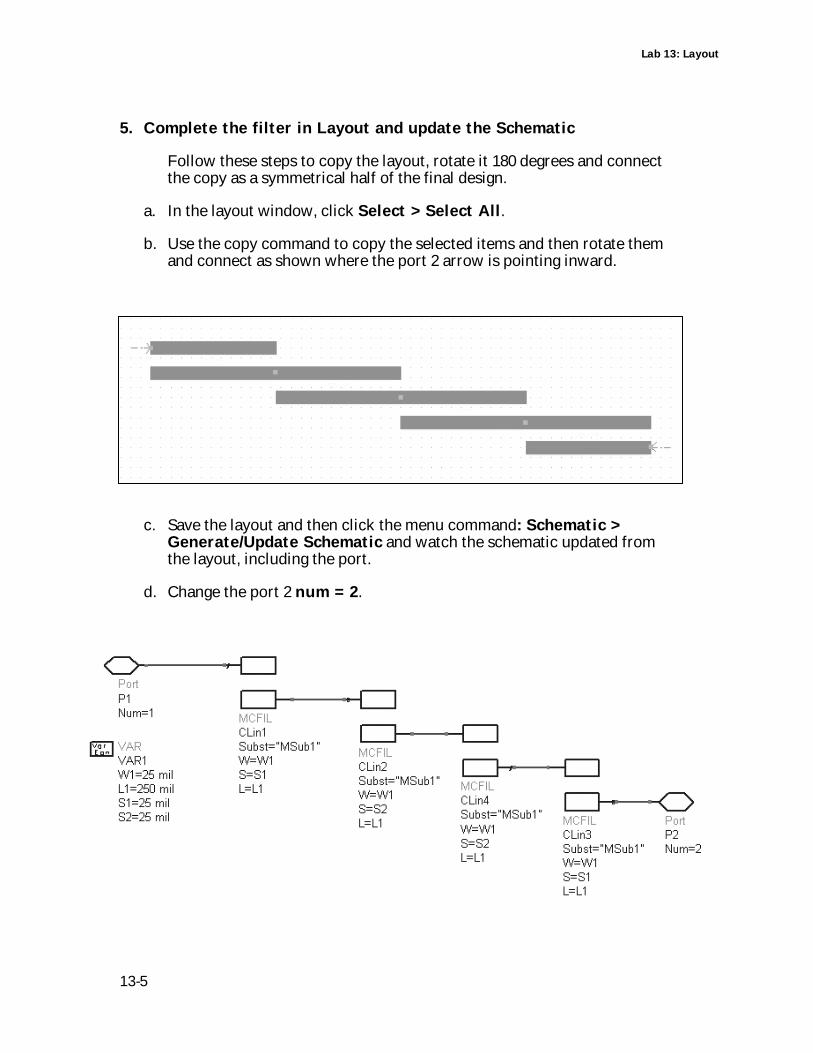
Lab 13: Layout
13-5
5. Complete the filter in Layout and update the Schematic
Follow these steps to copy the layout, rotate it 180 degrees and connectthe copy as a symmetrical half of the final design.
a. In the layout window, click Select > Select All.
b. Use the copy command to copy the selected items and then rotate themand connect as shown where the port 2 arrow is pointing inward.
c. Save the layout and then click the menu command: Schematic >Generate/Update Schematic and watch the schematic updated fromthe layout, including the port.
d. Change the port 2 num = 2.
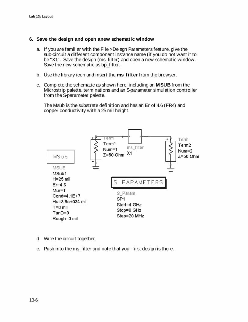
Lab 13: Layout
13-6
6. Save the design and open anew schematic window
a. If you are familiar with the File >Deisgn Parameters feature, give thesub-circuit a different component instance name (if you do not want it tobe “X1”. Save the design (ms_filter) and open a new schematic window.Save the new schematic as bp_filter.
b. Use the library icon and insert the ms_filter from the browser.
c. Complete the schematic as shown here, including an MSUB from theMicrostrip palette, terminations and an S-parameter simulation controllerfrom the S-parameter palette.
The Msub is the substrate definition and has an Er of 4.6 (FR4) andcopper conductivity with a 25 mil height.
d. Wire the circuit together.
e. Push into the ms_filter and note that your first design is there.
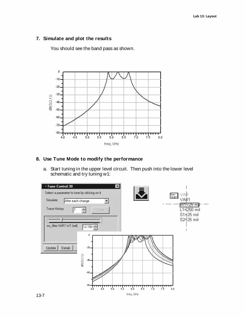
Lab 13: Layout
13-7
7. Simulate and plot the results
You should see the band pass as shown.
8. Use Tune Mode to modify the performance
a. Start tuning in the upper level circuit. Then push into the lower levelschematic and try tuning w1:
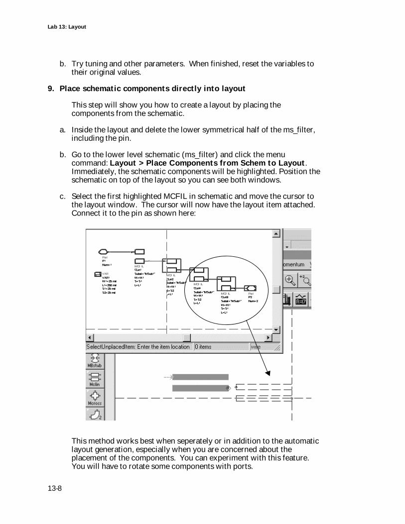
Lab 13: Layout
13-8
b. Try tuning and other parameters. When finished, reset the variables totheir original values.
9. Place schematic components directly into layout
This step will show you how to create a layout by placing thecomponents from the schematic.
a. Inside the layout and delete the lower symmetrical half of the ms_filter,including the pin.
b. Go to the lower level schematic (ms_filter) and click the menucommand: Layout > Place Components from Schem to Layout.Immediately, the schematic components will be highlighted. Position theschematic on top of the layout so you can see both windows.
c. Select the first highlighted MCFIL in schematic and move the cursor tothe layout window. The cursor will now have the layout item attached.Connect it to the pin as shown here:
This method works best when seperately or in addition to the automaticlayout generation, especially when you are concerned about theplacement of the components. You can experiment with this feature.You will have to rotate some components with ports.
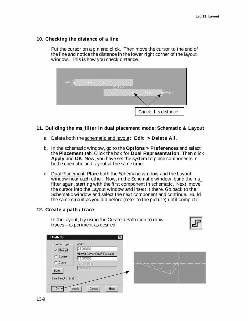
Lab 13: Layout
13-9
10. Checking the distance of a line
Put the cursor on a pin and click. Then move the cursor to the end ofthe line and notice the distance in the lower right corner of the layoutwindow. This is how you check distance.
11. Building the ms_filter in dual placement mode: Schematic & Layout
a. Delete both the schematic and layout: Edit > Delete All.
b. In the schematic window, go to the Options > Preferences and selectthe Placement tab. Click the box for Dual Representation. Then clickApply and OK. Now, you have set the system to place components inboth schematic and layout at the same time.
c. Dual Placement: Place both the Schematic window and the Layoutwindow near each other. Now, in the Schematic window, build the ms_filter again, starting with the first component in schematic. Next, movethe cursor into the Layout window and insert it there. Go back to theSchematic window and select the next component and continue. Buildthe same circuit as you did before (refer to the picture) until complete.
12. Create a path / trace
In the layout, try using the Create a Path icon to drawtraces – experiment as desired.
Check this distance
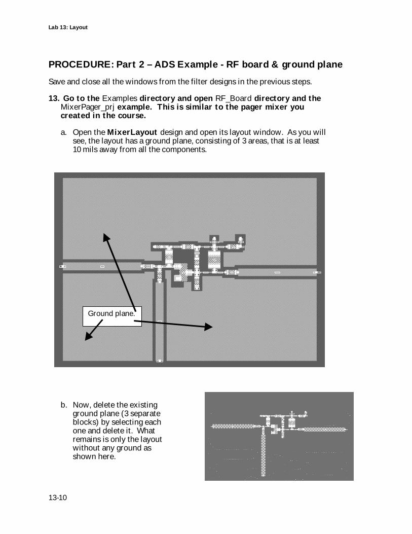
Lab 13: Layout
13-10
PROCEDURE: Part 2 – ADS Example - RF board & ground plane
Save and close all the windows from the filter designs in the previous steps.
13. Go to the Examples directory and open RF_Board directory and theMixerPager_prj example. This is similar to the pager mixer youcreated in the course.
a. Open the MixerLayout design and open its layout window. As you willsee, the layout has a ground plane, consisting of 3 areas, that is at least10 mils away from all the components.
b. Now, delete the existingground plane (3 separateblocks) by selecting eachone and delete it. Whatremains is only the layoutwithout any ground asshown here.
Ground plane.
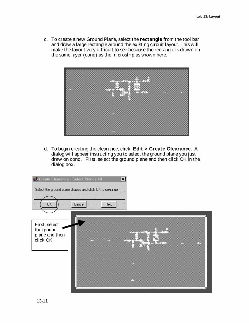
Lab 13: Layout
13-11
c. To create a new Ground Plane, select the rectangle from the tool barand draw a large rectangle around the existing circuit layout. This willmake the layout very difficult to see because the rectangle is drawn onthe same layer (cond) as the microstrip as shown here.
d. To begin creating the clearance, click: Edit > Create Clearance. Adialog will appear instructing you to select the ground plane you justdrew on cond. First, select the ground plane and then click OK in thedialog box.
First, selectthe groundplane and thenclick OK
Lab 13: Layout
13-12
e. When the next, enter the clearance value:10, but do NOT click OK or Apply yet.
f. Now, select the clearance area by rubberbanding (selecting) the circuit - which iseverything except the ground plane.
g. With the mixer pads and other items on all the layers selected, click theOK button and then cancel the dialogbox. Zoom in to see the result.
14. Cleaning up the Ground Plane
Use the cursor to selectthe clearance areawhich is the circuit –not the ground plane.
RESULT: circuit isselected and ready forthe clearance to becreated.
Lab 13: Layout
13-13
a. With the layout componentsselected, change the insertlayer to: pc1 in the top of thelayout window.
b. Turn on edge snap and vertex snap modes only. Turn all other snappingmodes off.
c. Zoom in on an area and draw rectangles on pc1 where you want toremove the cond material as shown:
d. Click Edit > Boolean Logical. When the dialog appears, set it asshown here:
e. Click the OK button and the pc1 area will be subtracted from the condlayer leaving the desired clearance. This is how the clean up is done.
Arearemoved.
Area toremove usingboolean logic.
Lab 13: Layout
13-14
15. OPTIONAL - Graphical Cell Compiler
For this final step, use the on-line manuals and the Step-by-Step procedure from theGCC Getting Started manual.
a. In the Main Window, click; HELP > Manuals.
b. Go to the Contents and select the GCC. Size the window so you canread the text and use the tutorial steps.
_____________________________________________________________
This concludes the layout lab exercise.