Embed Size (px)
Citation preview
IP6503S
V1.0 www.injoinic.com 1 / 11 Copyright © 2018, Injoinic Corp.
2.4A/3.1A OUTPUT STEP-DOWN CONVERTER
with DCP PROTOCOLS
1 Features
Synchronous step-down converter
Built-in Power MOSFETs
Wide Input Voltage Range, 8V to 32V
Output Voltage Range, 5V
Output Current, 2.4A/3.1A
Output Current Limit Protection
Conversion efficiency up to 94%
Soft-Start
Output Voltage Line Loss Compensation,
50mV@1A
Supports DCP(BC1.2, Apple, Samsung)
Multiple Safety Protections
Input Over-Current Protection, Output
Over-Current Protection, Input
Over/Under Voltage Protection, Short
Circuit Protection
Over Temperature Protection
Input Voltage Withstand up to 40V
ESD 4KV
2 Application
Car Charger
Charge Adapter
Intelligent Power Hub
3 Introduction
IP6503S is a synchronous step-down
converter with built-in power MOSFETs. IP6503S
supports DCP protocols (BC1.2, Apple and
Samsung), providing total solution to car charger,
charge adapter and intelligent power hub
applications.
IP6503S exhibits CV/CC characteristics. The
output in CV mode when the load current lower
than current limit, otherwise in CC mode, in which
the output voltage decreases as the load current
increases.
IP6503S supports output voltage
compensation due to the line loss. The output
voltage increases at 50mV@1A rate as the load
current increases.
IP6503S incorporates soft-start function to
prevent the inrush current during start-up.
IP6503S incorporates multiple safety
protections, such as input OV/UV, output
OV/UV/OC and SC protection.
The package of IP6503S is ESOP8.
IP6503S
V1.0 http://www.injoinic.com/ 2 / 11 Copyright © 2018, Injoinic Corp.
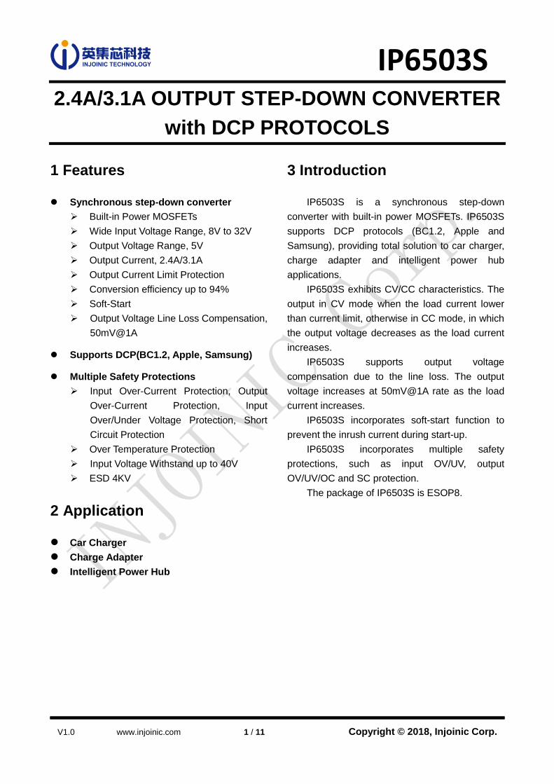
BSTVIN
SWNC
ESOP8
1
2
3
4 5
6
7
8
GND
DM
DP
VOUT
IP6503S
C3
VOUT
DM
DPC2
L1
VIN输入 8-32VL2
C1 C4
C5R1
Fig. 1 IP6503S Simplified Schematic
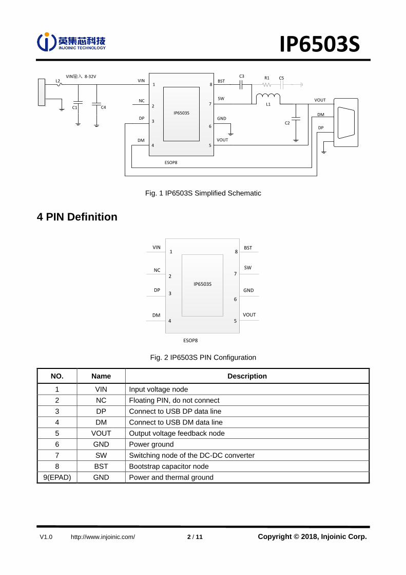
4 PIN Definition
BSTVIN
SWNC
ESOP8
1
2
3
4 5
6
7
8
GND
DM
DP
VOUT
IP6503S
Fig. 2 IP6503S PIN Configuration
NO. Name Description
1 VIN Input voltage node
2 NC Floating PIN, do not connect
3 DP Connect to USB DP data line
4 DM Connect to USB DM data line
5 VOUT Output voltage feedback node
6 GND Power ground
7 SW Switching node of the DC-DC converter
8 BST Bootstrap capacitor node
9(EPAD) GND Power and thermal ground
IP6503S
V1.0 http://www.injoinic.com/ 3 / 11 Copyright © 2018, Injoinic Corp.
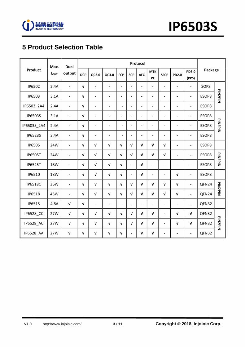
5 Product Selection Table
Product Max.
IOUT
Dual
output
Protocol
Package DCP QC2.0 QC3.0 FCP SCP AFC
MTK
PE SFCP PD2.0
PD3.0
(PPS)
IP6502 2.4A - √ - - - - - - - - - SOP8 PIN
2P
IN
IP6503 3.1A - √ - - - - - - - - - ESOP8
IP6503_2A4 2.4A - √ - - - - - - - - - ESOP8
IP6503S 3.1A - √ - - - - - - - - - ESOP8 PIN
2P
IN
IP6503S_2A4 2.4A - √ - - - - - - - - - ESOP8
IP6523S 3.4A - √ - - - - - - - - - ESOP8
IP6505 24W - √ √ √ √ √ √ √ √ - - ESOP8
IP6505T 24W - √ √ √ √ √ √ √ √ - - ESOP8
PIN
2P
IN IP6525T 18W - √ √ √ √ - √ - - - - ESOP8
IP6510 18W - √ √ √ √ - √ - - √ - ESOP8
IP6518C 36W - √ √ √ √ √ √ √ √ √ - QFN24
PIN
2P
IN IP6518 45W - √ √ √ √ √ √ √ √ √ - QFN24
IP6515 4.8A √ √ - - - - - - - - - QFN32
IP6528_CC 27W √ √ √ √ √ √ √ √ - √ √ QFN32 PIN
2P
IN
IP6528_AC 27W √ √ √ √ √ √ √ √ - √ √ QFN32
IP6528_AA 27W √ √ √ √ √ - √ √ - - - QFN32
IP6503S
V1.0 http://www.injoinic.com/ 4 / 11 Copyright © 2018, Injoinic Corp.
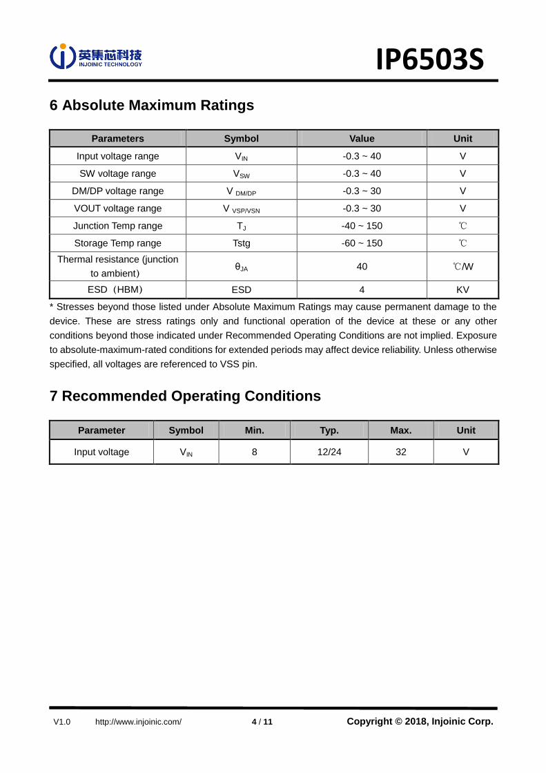
6 Absolute Maximum Ratings
Parameters Symbol Value Unit
Input voltage range VIN -0.3 ~ 40 V
SW voltage range VSW -0.3 ~ 40 V
DM/DP voltage range V DM/DP -0.3 ~ 30 V
VOUT voltage range V VSP/VSN -0.3 ~ 30 V
Junction Temp range TJ -40 ~ 150 ℃
Storage Temp range Tstg -60 ~ 150 ℃
Thermal resistance (junction
to ambient) θJA 40 ℃/W
ESD(HBM) ESD 4 KV
* Stresses beyond those listed under Absolute Maximum Ratings may cause permanent damage to the
device. These are stress ratings only and functional operation of the device at these or any other
conditions beyond those indicated under Recommended Operating Conditions are not implied. Exposure
to absolute-maximum-rated conditions for extended periods may affect device reliability. Unless otherwise
specified, all voltages are referenced to VSS pin.
7 Recommended Operating Conditions
Parameter Symbol Min. Typ. Max. Unit
Input voltage VIN 8 12/24 32 V
IP6503S
V1.0 http://www.injoinic.com/ 5 / 11 Copyright © 2018, Injoinic Corp.
8 Electrical Charateristics
TA=25℃,L=22uH,COUT=220uF E-cap(About 100mΩ ESR),VIN=12V,VOUT=5V, otherwise specified
Parameter Symbol Test Condition Min. Typ. Max. Unit
Input System
Input voltage VIN 8 12 32 V
Input under
voltage threshold VIN-UV
8.1 V
hysteresis 0.3 V
Input over
voltage threshold VIN-OV
32 V
hysteresis 0.2 V
Input quiescent
current IQ VIN=12V, VOUT=5V@0A 1 mA
Converter System
High side
MOSFET on
resistance
RDS(ON) 100 mΩ
Low side
MOSFET on
resistance
RDS(ON) 80 mΩ
Switching
frequency FSW 150 KHz
Output System
Output voltage VOUT 4.75 5 5.25 V
Output voltage
ripple ΔVOUT VIN=12V,VOUT=5V@3A 150 mV
Soft-start time TSS VIN=12V,VOUT=5V 10 ms
Line loss
compensation VCOMP VIN=12V,VOUT=5V,IOUT=3A 180 mV
Current limit in
CC mode IOUT VIN=12V,VOUT=5V 3.1 A
Output hiccup
restart voltage VOUT
When output enters CC mode,
output hiccup restart voltage 4 V
Thermal
shutdown Temp. TOTP 150 ℃
Thermal
shutdown Temp.
hysteresis
ΔTOTP 40 ℃
IP6503S
V1.0 http://www.injoinic.com/ 6 / 11 Copyright © 2018, Injoinic Corp.
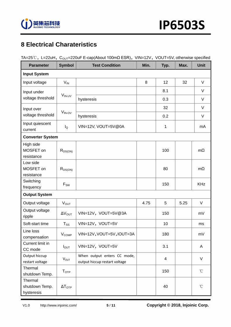
9 Detailed Description
Synchronous Step-Down Converter
The IP6503S is a synchronous step-down converter with built-in power MOSFETs. .IP6503S
supports wide input voltage range (8-32V) and 5V output at 3.1A Max. load current. The switching
frequency is 150KHz. The conversion efficiency is up to 94% at VIN=12V, VOUT=5V@2A.
The efficiency under different input voltage and load current is shown in Fig. 3. Fig. 4 shows the
output voltage characteristics under different load current.
Fig. 3 IP6503S Conversion Efficiency
Fig.4 IP6503S Output Voltage Characteristics
87
88
89
90
91
92
93
94
95
96
0 500 1000 1500 2000 2500 3000 3500
n(%
)
Iout(mA)
IP6503S Efficiency Curve
VIN=12V
VIN=24V
0
1
2
3
4
5
6
0 500 1000 1500 2000 2500 3000 3500 4000
Vout(
V)
Iout(mA)
IP6503S Output Voltage Curve
VIN=12V
VIN=24V
IP6503S
V1.0 http://www.injoinic.com/ 7 / 11 Copyright © 2018, Injoinic Corp.
Output Voltage Line Loss Compensation
IP6503S supports output line loss compensation. The output voltage increases at 50mV/1A rate.
CC/CV Characteristics
IP6503S exhibits CV/CC characteristics. The output in CV mode when the load current lower than
current limit, otherwise in CC mode, in which the output voltage decreases as the load current increases.
Protections
IP6503S monitors voltage on VIN. If the voltage is lower than 8.1V, IP6503S enters standby mode,
and shuts down the converter. If the voltage is higher than 32V, IP6503S detects over voltage, and then
shuts down the converter. When VIN decreases 0.2V lower than the over voltage threshold, IP6503S
resumes the output voltage.
IP6503S also monitors voltage on VOUT. If the voltage is lower than 4V, IP6503S detects output
under voltage, and then shuts down the converter. During output under voltage protection, IP6503S
enters hiccup mode, and restarts the converter every 2 seconds.
IP6503S incorporates short circuit protection. After 8ms from start-up, if VOUT is lower than 4V,
IP6503S detects output short circuit, then shutting down the converter, and enters hiccup mode.
IP6503S restarts the converter every 2 seconds.
IP6503S detects over temperature when the chip temperature is higher than 150℃. IP6503S shuts
down the converter and restarts the every 2 seconds. When the chip temperature decreases below 110℃,
IP6503S returns to normal state.
Charge Protocols
IP6503S supports DCP (BC1.2, Apple, Samsung).
IP6503S
V1.0 http://www.injoinic.com/ 8 / 11 Copyright © 2018, Injoinic Corp.
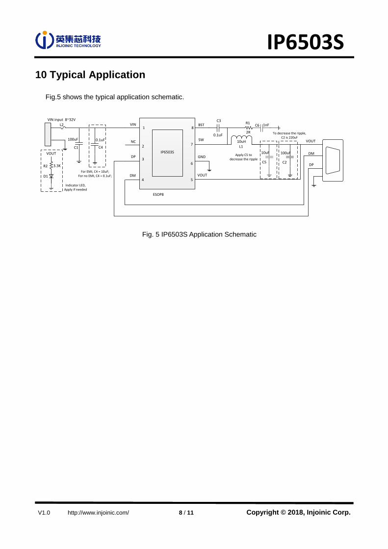
10 Typical Application
Fig.5 shows the typical application schematic.
2R
BSTVIN
SWNC
ESOP8
1
2
3
4 5
6
7
8
GND
DM
DP
VOUT
IP6503S
C3
VOUT
DM
DPC2
L1
L2
C1 C4
VOUT
3.3KR2
D1
1nFC6R1
10uH
10uF
C5
100uF
100uF 0.1uF0.1uF
For EMI, C4 = 10uF;For no EMI, C4 = 0.1uF;
Indicator LED,Apply if needed
VIN input 8~32V
Apply C5 to decrease the ripple
To decrease the ripple, C2 is 220uF
Fig. 5 IP6503S Application Schematic
IP6503S
V1.0 http://www.injoinic.com/ 9 / 11 Copyright © 2018, Injoinic Corp.
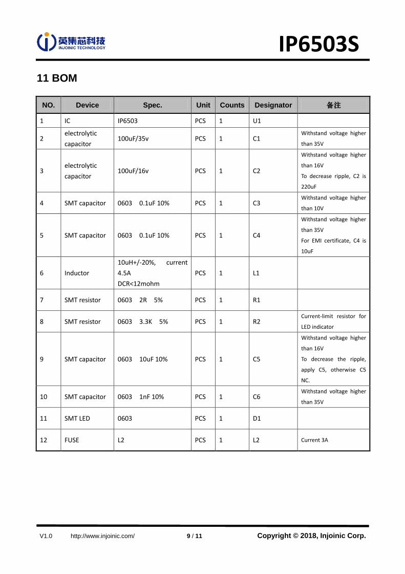
11 BOM
NO. Device Spec. Unit Counts Designator 备注
1 IC IP6503 PCS 1 U1
2 electrolytic
capacitor 100uF/35v PCS 1 C1
Withstand voltage higher
than 35V
3 electrolytic
capacitor 100uF/16v PCS 1 C2
Withstand voltage higher
than 16V
To decrease ripple, C2 is
220uF
4 SMT capacitor 0603 0.1uF 10% PCS 1 C3 Withstand voltage higher
than 10V
5 SMT capacitor 0603 0.1uF 10% PCS 1 C4
Withstand voltage higher
than 35V
For EMI certificate, C4 is
10uF
6 Inductor
10uH+/-20%, current
4.5A
DCR<12mohm
PCS 1 L1
7 SMT resistor 0603 2R 5% PCS 1 R1
8 SMT resistor 0603 3.3K 5% PCS 1 R2 Current-limit resistor for
LED indicator
9 SMT capacitor 0603 10uF 10% PCS 1 C5
Withstand voltage higher
than 16V
To decrease the ripple,
apply C5, otherwise C5
NC.
10 SMT capacitor 0603 1nF 10% PCS 1 C6 Withstand voltage higher
than 35V
11 SMT LED 0603 PCS 1 D1
12 FUSE L2 PCS 1 L2 Current 3A
IP6503S
V1.0 http://www.injoinic.com/ 10 / 11 Copyright © 2018, Injoinic Corp.
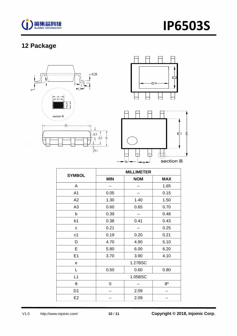
12 Package
SYMBOL MILLIMETER
MIN NOM MAX
A -- -- 1.65
A1 0.05 -- 0.15
A2 1.30 1.40 1.50
A3 0.60 0.65 0.70
b 0.39 -- 0.48
b1 0.38 0.41 0.43
c 0.21 -- 0.25
c1 0.19 0.20 0.21
D 4.70 4.90 5.10
E 5.80 6.00 6.20
E1 3.70 3.90 4.10
e 1.27BSC
L 0.50 0.60 0.80
L1 1.05BSC
θ 0 -- 8º
D1 -- 2.09 --
E2 -- 2.09 --
IP6503S
V1.0 http://www.injoinic.com/ 11 / 11 Copyright © 2018, Injoinic Corp.
IMPORTANT NOTICE
INJOINIC TECHNOLOGY and its subsidiaries reserve the right to make corrections, enhancements,
improvements and other changes to its semiconductor products and services. Buyers should obtain the latest
relevant information before placing orders and should verify that such information is current and complete. All
semiconductor products (also referred to herein as “components”) are sold subject to INJOINIC TECHNOLOGY's
terms and conditions of sale supplied at the time of order acknowledgment.
INJOINIC TECHNOLOGY assumes no liability for applications assistance or the design of Buyers' products.
Buyers are responsible for their products and applications using INJOINIC TECHNOLOGY's components. To
minimize the risks associated with Buyers' products and applications, Buyers should provide adequate design and
operating safeguards.
Buyer acknowledges and agrees that it is solely responsible for compliance with all legal, regulatory and
safety-related requirements concerning its products, and any use of INJOINIC TECHNOLOGY's components in its
applications, notwithstanding any applications-related information or support that may be provided by INJOINIC
TECHNOLOGY. Buyer represents and agrees that it has all the necessary expertise to create and implement
safeguards which anticipate dangerous consequences of failures, monitor failures and their consequences, lessen
the likelihood of failures that might cause harm and take appropriate remedial actions. Buyer will fully indemnify
INJOINIC TECHNOLOGY and its representatives against any damages arising out of the use of any INJOINIC
TECHNOLOGY's components in safety-critical applications.
Reproduction of significant portions of INJOINIC TECHNOLOGY's information in INJOINIC TECHNOLOGY's data
books or data sheets is permissible only if reproduction is without alteration and is accompanied by all associated
warranties, conditions, limitations, and notices. INJOINIC TECHNOLOGY is not responsible or liable for such altered
documentation. Information of third parties may be subject to additional restrictions.
INJOINIC TECHNOLOGY will update this document from time to time. The actual parameters of the product
may vary due to different models or other items. This document voids all express and any implied warranties.
Resale of INJOINIC TECHNOLOGY's components or services with statements different from or beyond the
parameters stated by INJOINIC TECHNOLOGY for that component or service voids all express and any implied
warranties for the associated INJOINIC TECHNOLOGY's component or service and is an unfair and deceptive
business practice. INJOINIC TECHNOLOGY is not responsible or liable for any such statements.


