Embed Size (px)
Citation preview
arX
iv:1
201.
2752
v1 [
cond
-mat
.mes
-hal
l] 1
3 Ja
n 20
12
Intermediate state switching dynamics in magnetic
double layer nanopillars grown by molecular beam
epitaxy
N. Musgensa,c, T. Maassena,c,1, E. Maynickea,c, S. Rizwan Alia,c, A. Heissb,c,R. Ghadimib,c, J. Mayerb,c, G. Guntherodta,c, B. Beschotena,c,∗
aII. Institute of Physics, RWTH Aachen University, 52056 Aachen, GermanybCentral Facility for Electron Microscopy, RWTH Aachen University, 52056 Aachen,
GermanycJARA-Fundamentals of Future Information Technology, Julich-Aachen
Abstract
We observe a stable intermediate resistance switching state in the currentperpendicular to plane geometry for all Co/Cu/Co double layer nanopillarjunctions grown by molecular beam epitaxy. This novel state has a resistancebetween the resistances of the parallel and antiparallel alignment of both Co-layer magnetizations. The state, which originates from an additional in-planemagnetic easy axis, can be reached by spin transfer torque switching or by anexternal magnetic field. In addition to spin torque-induced coherent small-angle spin wave modes we observe a broad microwave emission spectrum. Thelatter is attributed to incoherent magnetic excitations that lead to a switchingbetween the intermediate state and the parallel or antiparallel alignment ofboth ferromagnetic layers. We conclude that the additional magnetic easyaxis suppresses a stable trajectory of coherent large-angle precession, whichis not observed in our samples.
Keywords:
∗Corresponding authorEmail address: [email protected] (B. Beschoten)
1Current address: Physics of Nanodevices, Zernike Institute for Advanced Materials,University of Groningen, The Netherlands
Preprint submitted to Elsevier January 16, 2012
1. Introduction
A spin-polarized current passing through a ferromagnetic layer can ex-ert a spin transfer torque on its magnetization [1, 2, 3, 4, 5]. The torqueis of particular interest, since it opens the way to an efficient control of themagnetic moments of a nanomagnet in applications such as nonvolatile mag-netic memories and tunable microwave oscillators. Most previous work hasbeen focused on polycrystalline nanopillars consisting of ferromagnet/normalmetal/ferromagnet (FM/NM/FM) layered systems with unequal FM layerthicknesses. The thicker FM layer is used to spin-polarize the current whenflowing in the perpendicular-to-plane direction. The second NM/FM inter-face may exhibit a net spin torque on the thinner FM due to the absorptionof a transverse spin component. Depending on both the current and theexternal magnetic field the spin torque can either switch the thin FM layerhysteretically between the parallel (P) and antiparallel (AP) alignment ofboth magnetizations [6] or excite the thin layer in a variety of distinguishabledynamical modes [7, 8, 9]. In epitaxial bilayer samples, however, magneto-crystalline anisotropy can reveal an additional anisotropy axis resulting intwo-step magnetization switching effects [10, 11].
In this work, we study Co/Cu/Co-nanopillars grown by molecular beamepitaxy (MBE) using quasi-static and high-frequency resistance measure-ments at room temperature. The goal is to establish a field-current phasediagram of the differential resistance and the microwave emission of thesesjunctions. We observe a stable intermediate resistance state (IS) in betweenthe P and the AP alignment of both ferromagnetic layers. We discuss theorigin of the IS and its effect on the magnetization dynamics of the thin Colayer. We find that the novel IS suppresses coherent large-angle precessionalmagnetization dynamics favoring incoherent magnetization excitations.
2. Materials and methods
Samples have been fabricated using focused ion-beam assisted nanostencilmasks [12, 13]. The thin film stack of Co(3 nm)/Cu/Co(15 nm) is depositedby MBE in prefabricated undercut templates on top of a sputtered Pt bottomelectrode (BE) (Fig. 1(a), inset). The presented experimental data have beenobtained from a nanopillar with an elliptical cross section of 30×90 nm2 anda 15 nm thick Cu spacer. While we focus in this paper on the results obtainedon a single sample, the existence of the intermediate resistance state is inde-pendent of the Cu spacer thickness (10−25 nm) and the cross sectional area
2
950 Oe
500 Oe
25 Oe
-25 Oe
11 kOe
I (mA)84-8 -4 0
dV
/dI (Ω
)
6.2
7.8
6.6
7.0
7.4
8.2
dV
/dI (Ω
)
-2 0 1 2-1H (kOe)
6.2
6.3
6.4
0.1 mA
2
-2
-1
0
1
H (
kO
e)
-8 -4 0 4I (mA)
∆dV/dI (Ω)-0.5 0.50
8
P
AP
ISP/IS
D+
D-
P
ISP/IS
D+
dV
/dI (Ω
)
-6 0 3 6-3I (mA)
6.2
6.3
6.4-25 Oe25 Oe
500 Oe
AP
P
IS
(a) (b)
(c) (d)
Cu - TE
Si substrate
SiO2
Co
Pt - BE
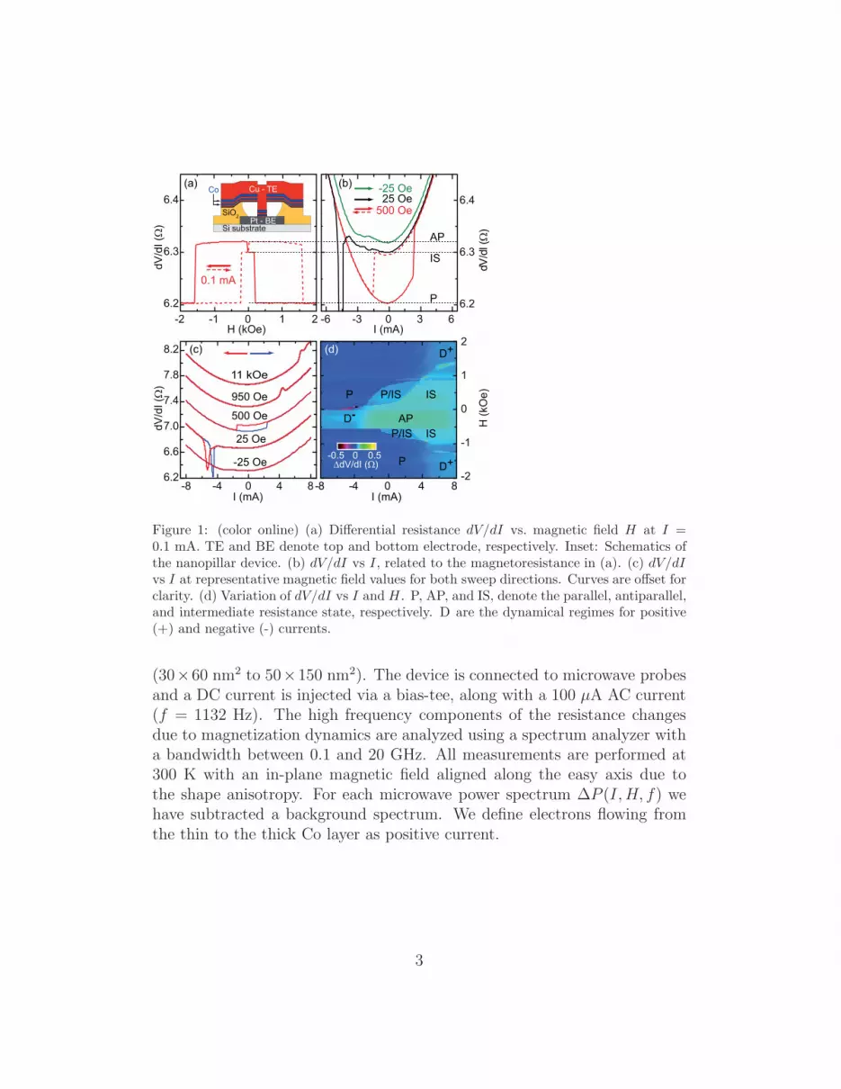
Figure 1: (color online) (a) Differential resistance dV/dI vs. magnetic field H at I =0.1 mA. TE and BE denote top and bottom electrode, respectively. Inset: Schematics ofthe nanopillar device. (b) dV/dI vs I, related to the magnetoresistance in (a). (c) dV/dIvs I at representative magnetic field values for both sweep directions. Curves are offset forclarity. (d) Variation of dV/dI vs I and H . P, AP, and IS, denote the parallel, antiparallel,and intermediate resistance state, respectively. D are the dynamical regimes for positive(+) and negative (-) currents.
(30×60 nm2 to 50×150 nm2). The device is connected to microwave probesand a DC current is injected via a bias-tee, along with a 100 µA AC current(f = 1132 Hz). The high frequency components of the resistance changesdue to magnetization dynamics are analyzed using a spectrum analyzer witha bandwidth between 0.1 and 20 GHz. All measurements are performed at300 K with an in-plane magnetic field aligned along the easy axis due tothe shape anisotropy. For each microwave power spectrum ∆P (I,H, f) wehave subtracted a background spectrum. We define electrons flowing fromthe thin to the thick Co layer as positive current.
3
3. Results
Fig. 1(a) shows a typical field-driven magnetoresistance (MR) measure-ment at small positive current. When H is reduced from H = 2 kOe (redsolid line) the dipolar coupling between both Co layers causes the thin layerto switch abruptly already at H1 = 200 Oe from the low resistance P state toa higher resistance state. In contrast to previous studies [12, 14] this higherresistance state does not correspond to the AP state but to a novel stableIS with a resistance value lower than the AP state. The latter state is onlyreached at H2 = −40 Oe, which is the coercive field of the thick layer. As thenegative H is increased further the thin layer switches at H3 = −1570 Oein one step to the reversed P configuration. From the switching fields H1
and H3 we can extract [15] the coupling strength between the two FM layersHcoupling = 885 Oe and the coercive field of the thin layer HC,thin = 685 Oe,consistent with previous studies of Co-based nanopillars [7, 14].
In Fig. 1(b) we depict the differential resistance dV/dI of the junction asa function of I for representative values of H . The system was first set intothe P state at I = −8 mA and H = 2 kOe. For H = 500 Oe we clearlyobserve current induced hysteretic switching. In comparison with the field-driven MR (Fig. 1(a)) it is obvious that the high resistance state is not theAP state but rather corresponds to the IS. Note that even for current valuesup to 15 mA the AP state is not accessible (not shown). Such a behaviorhas not been observed for sputtered samples [6, 12, 16]. We observe a similarbehavior in all our junctions.
For large positive currents and fields we observe the well known peaks inthe differential resistance (in Fig. 1(c)), which indicate the onset of spin wavegeneration in the thin layer [7]. At small magnetic fields (see H = 25 Oecurve in Fig. 1(b) and (c)) pronounced non-hysteretic dips are seen in thedV/dI curves. As our sample is in the IS and not in the AP state, it willbe interesting to explore the spin wave dynamics in this regime. As the fieldpolarity is inverted (see, e.g., H = −25 Oe in Fig. 1(b)) the system switchesinto the AP state. In this state only a small resistance decrease appears atnegative I.
The current induced transport is summarized in a transport phase dia-gram in Fig. 1(d). The three distinct resistance states (P, IS, AP) and theexpected dynamics regions (D) are marked. The major difference comparedto previous phase diagrams of sputtered Co/Cu/Co samples [14, 17] is thatour samples can be driven by current only into the IS and not into the AP
4
5 nm
Cu
Co
Co20 nm(a) (b)
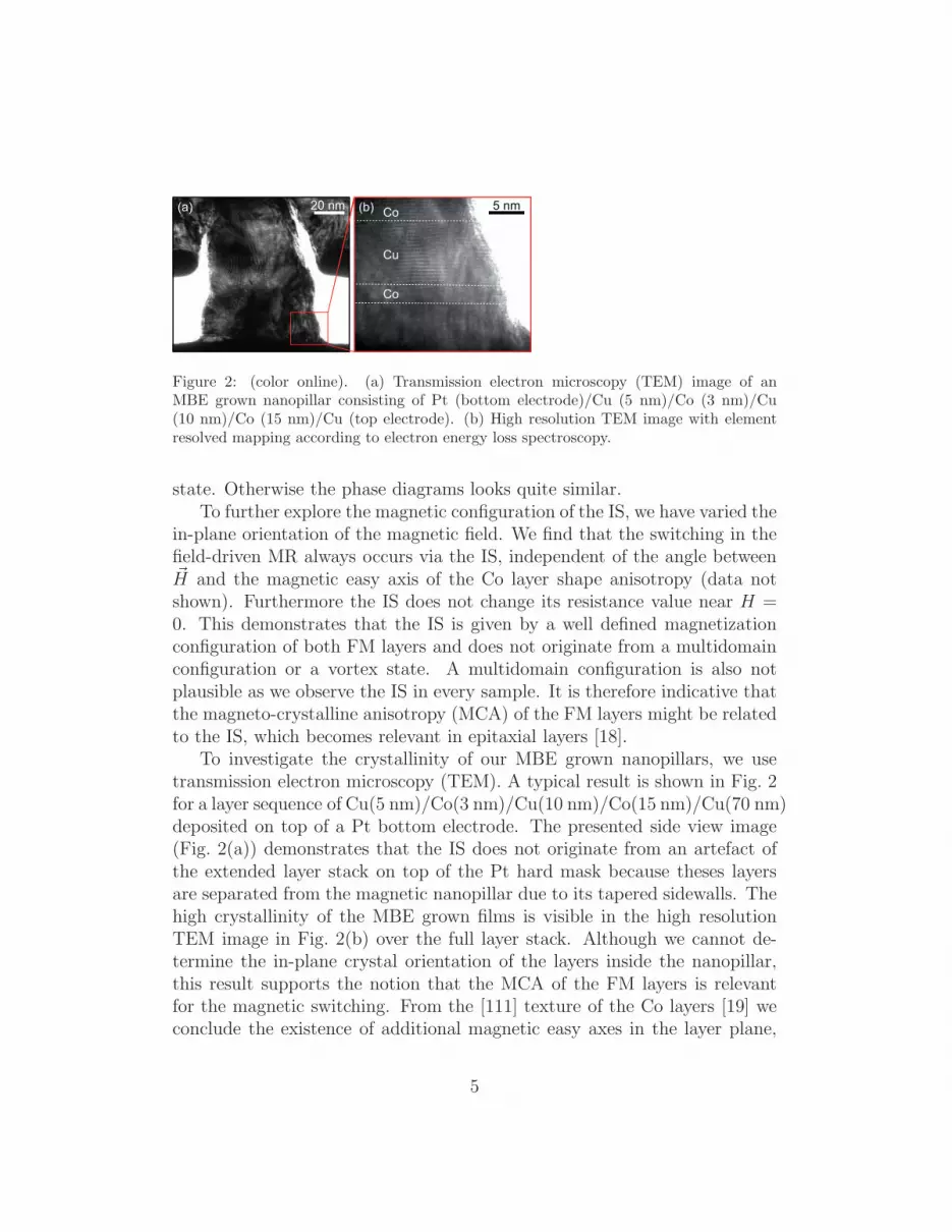
Figure 2: (color online). (a) Transmission electron microscopy (TEM) image of anMBE grown nanopillar consisting of Pt (bottom electrode)/Cu (5 nm)/Co (3 nm)/Cu(10 nm)/Co (15 nm)/Cu (top electrode). (b) High resolution TEM image with elementresolved mapping according to electron energy loss spectroscopy.
state. Otherwise the phase diagrams looks quite similar.To further explore the magnetic configuration of the IS, we have varied the
in-plane orientation of the magnetic field. We find that the switching in thefield-driven MR always occurs via the IS, independent of the angle between~H and the magnetic easy axis of the Co layer shape anisotropy (data notshown). Furthermore the IS does not change its resistance value near H =0. This demonstrates that the IS is given by a well defined magnetizationconfiguration of both FM layers and does not originate from a multidomainconfiguration or a vortex state. A multidomain configuration is also notplausible as we observe the IS in every sample. It is therefore indicative thatthe magneto-crystalline anisotropy (MCA) of the FM layers might be relatedto the IS, which becomes relevant in epitaxial layers [18].
To investigate the crystallinity of our MBE grown nanopillars, we usetransmission electron microscopy (TEM). A typical result is shown in Fig. 2for a layer sequence of Cu(5 nm)/Co(3 nm)/Cu(10 nm)/Co(15 nm)/Cu(70 nm)deposited on top of a Pt bottom electrode. The presented side view image(Fig. 2(a)) demonstrates that the IS does not originate from an artefact ofthe extended layer stack on top of the Pt hard mask because theses layersare separated from the magnetic nanopillar due to its tapered sidewalls. Thehigh crystallinity of the MBE grown films is visible in the high resolutionTEM image in Fig. 2(b) over the full layer stack. Although we cannot de-termine the in-plane crystal orientation of the layers inside the nanopillar,this result supports the notion that the MCA of the FM layers is relevantfor the magnetic switching. From the [111] texture of the Co layers [19] weconclude the existence of additional magnetic easy axes in the layer plane,
5
non-collinear with the easy axis of the shape anisotropy.Consequently, the magnetic switching of the thin Co layer from the P state
into the IS is consistent with switching between the easy axis direction dueto the shape anisotropy and an easy axis direction of the MCA. In order toestimate the resulting angle in between both Co-magnetization directions inthe IS configuration we use for simplicity the sin2(ϕ)-dependence of the giantmagnetoresistance effect for symmetrical systems consisting of 2 identicalferromagnetic layers [20]. For the resistance value of the IS in Fig. 1 (a) thisgives an angle of ϕ ≈ 130. It is important to emphasize that the relativeresistance rIS = RIS−RP
RAP−RP
of the IS does vary from junction to junction forotherwise identical layer stacks. This indicates a variation of the MCA axisrelative to the shape anisotropy direction for different junctions which isprobably related to a random growth orientation on the sputtered Pt bottomelectrode.
We next focus on the spin torque-induced spin wave dynamics. In Fig. 3we present frequency domain studies of microwave emission detected nearthe current induced magnetization instabilities as previously identified in thedV/dI vs. I curves in Fig. 1(b),(c). The correlation between the differentialresistance changes and the integrated microwave power is displayed in themicrowave emission phase diagram (Fig. 3(a)). It shows different regimes ofexcitations depending on both current and magnetic field polarity [28]. Onthe one hand, we observe microwave emission at negative currents in both thedip regime Ddip for small positive fields (Fig. 1(c)) and the D−-regime. Onthe other hand, we detect magnetic excitations at large positive currents andmagnetic fields |H| > 1.2 kOe (D+-regimes). These excitations are linked topeaks in dV/dI (Fig. 1(c)), i.e. to an increase in junction resistance.
In Fig. 3(c) we depict microwave spectra for various negative currentsat a small magnetic field of −0.1 kOe (D−-regime). For currents below theemission threshold of −2 mA, we detect microwave emission spectra extend-ing from 100 MHz up to 9 GHz. Their overall amplitude ∆P increases withincreasing negative current values (Fig. 3(c)), but surprisingly, there is nofrequency shift neither with current nor with magnetic field. Note that thesharp minima in ∆P observed at several frequencies are visible in all mea-sured spectra independent of current. They are not related to the samplebut are rather due to absorption in the high frequency electrical circuit.
Similarly broad emission spectra are also observed in the D+-regimes (seeH = ±1.4 kOe, I = 8 mA in Fig. 3(b)) as well as in the dip regime Ddip (seeH = 25 Oe emission data in Fig. 3(b) and in Fig. 3(e) with a continuum at low
6
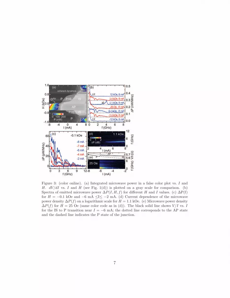
Figure 3: (color online). (a) Integrated microwave power in a false color plot vs. I andH . dV/dI vs. I and H (see Fig. 1(d)) is plotted on a gray scale for comparison. (b)Spectra of emitted microwave power ∆P (I,H, f) for different H and I values. (c) ∆P(f)for H = −0.1 kOe and −6 mA ≤I≤ −2 mA. (d) Current dependence of the microwavepower density ∆P (f) on a logarithmic scale forH = 1.1 kOe. (e) Microwave power density∆P (f) for H = 25 Oe (same color code as in (d)). The black solid line shows V/I vs. Ifor the IS to P transition near I = −6 mA; the dotted line corresponds to the AP stateand the dashed line indicates the P state of the junction.
7
frequencies). In the latter case the microwave emission abruptly disappearsnear I = −6 mA when the magnetization configuration switches from the ISinto the P state. This switching is reflected in the corresponding change inresistance V/I vs. I included in Fig. 3(e). We interpret these broad microwaveemission spectra (Fig. 3(b,c,e)) as a result of incoherent spin-wave excitationsdue to spin transfer torque that lead to a switching [22, 23] between theintermediate state IS and the P or AP state of both ferromagnetic layers.The incoherence is attributed to inhomogeneities in local fields giving rise todistributions of local precession frequencies [8]. Hence, we conclude that theadditional easy axis due to the MCA of the thin Co layer suppresses a stabletrajectory, i.e. a well defined mode frequency of the coherent large-angledynamics, which was previously found in polycrystalline samples [17, 7]. Notethat the observed incoherent magnetization dynamics has not been reportedin frequency domain studies on single-crystalline nanopillars [24].
In addition to the incoherent magnetization dynamics we also observe co-herent small angle precessional dynamics of the thin Co layer in a small rangeof positive magnetic fields for positive currents slightly above the hystereticswitching regime (see H = 1.1 kOe, 5 mA≤ I ≤ 8 mA in Fig. 3(a,b,d)). Thespectra have a typical linewidth of FWHM ≈ 300 MHz. Independent ofthe magnetic field we only observe spin wave frequencies which increase withincreasing current magnitude. Such behavior is characteristic of out-of-planeprecessional modes [25]. In contrast, we do not observe in-plane precessionswhich could be identified by a decrease of their excitation frequency withincreasing current [25]. These findings support the notion that in-plane pre-cession of the thin layer magnetization is inhibited by the intermediate state.
For high magnetic fields |H| > 4 kOe and large positive currents themicrowave emission continuously evolves into a spectrum resembling 1/f noisewithout any high-frequency peaks. The reason lies in the chaotic characterof the incoherent spin wave excitations [8] as seen in Fig. 3(b) for H =±12 kOe. This regime is correlated with an increase in junction resistance(Fig. 1(c)). The so-called static high resistance state has also been observedpreviously in systems without an intermediate resistance state [26] and hasits origin in an out-of-plane tilted magnetization of the thin Co layer, wherethe spin torque and the torque by the external magnetic field compensateeach other [27, 28, 29]. The out-of-plane tilted magnetization therefore yieldsa transition to a regime of dynamics not affected by the in-plane anisotropies.
8
4. Conclusions
In conclusion, MBE-grown Co/Cu/Co magnetic double layer nanopillarjunctions show a stable intermediate resistance state with a resistance valuebetween the resistances of the parallel and antiparallel alignments of bothCo layers. It results from magnetic switching of the thin Co layer into an ad-ditional in-plane easy axis, which is non-collinear with the shape anisotropyaxis. We have shown that the additional easy axis may originate from amagneto-crystalline anisotropy due to the texture or enhanced crystallinityof the layer stack. For magnetic fields smaller than the coercive field of thethin Co layer, we observe hysteretic switching between the parallel magne-tization configuration and the intermediate resistance state. However, nocurrent induced transitions into the AP state have been observed. Althoughthe current induced resistance changes agree qualitatively with dipolar cou-pled double magnetic layer nanopillars without an intermediate state, nocoherent large-angle precessional motion of the thin-layer magnetization hasbeen observed. Instead we detect broad microwave emission spectra, whichwe attribute to incoherent excitations that lead to switching between theintermediate state and the parallel or antiparallel magnetization configura-tions.
We acknowledge useful discussions with B. Ozyilmaz. This work wassupported by DFG through SPP 1133 and by HGF.
References
[1] J. C. Slonczewski, J. Magn. Magn. Mater 159 (1996) L1.
[2] L. Berger, Phys. Rev. B 54 (1996) 9353.
[3] M. Tsoi, A. G. M. Jansen, J. Bass, et al., Phys. Rev. Lett. 80 (1998)4281.
[4] E. B. Myers, D. C. Ralph, J. A. Katine, et al., Science 285 (1999) 867.
[5] M. D. Stiles, A. Zangwill, Phys. Rev. B 66 (2002) 014407.
[6] J. A. Katine, F. J. Albert, R. A. Buhrman, et al., Phys. Rev. Lett. 84(2000) 3149.
[7] S. I. Kiselev, J. C. Sankey, I. N. Krivorotov, et al., Nature 425 (2003)380.
9

[8] K.-J. Lee, A. Deac, O. Redon, et al., Nature Mat. 3 (2004) 877.
[9] S. I. Kiselev, J. C. Sankey, I. N. Krivorotov, et al., Phys. Rev. Lett. 93(2004) 036601.
[10] H. Dassow, R. Lehndorff, D. E. Burgler, et al., Appl. Phys. Lett. 89(2006) 222511.
[11] R. Lehndorff, M. Buchmeier, D. E. Burgler, et al. Phys. Rev. B 76 (2007)214420.
[12] B. Ozyilmaz, G. Richter, N. Musgens, et al., J. Appl. Phys. 101 (2007)063920.
[13] N. Musgens, E. Maynicke, M. Weidenbach, et al., J. Phys. D 41 (2008)164011.
[14] S. Urazhdin, H. Kurt, J. W. P. Pratt, et al., Appl. Phys. Lett. 83 (2003)114.
[15] Hcoupling =12(|H3|+ |H1|) ; HC,thin = 1
2(|H3| − |H1|).
[16] F. J. Albert, J. A. Katine, R. A. Buhrman, et al., Appl. Phys. Lett. 77(2000) 3809.
[17] J. C. Sankey, I. N. Krivorotov, S. I. Kiselev, et al., Phys. Rev. B 72(2005) 224427.
[18] R. Lehndorff, D. E. Burgler, S. Gliga, et al., Phys. Rev. B 80 (2009)054412.
[19] XRD measurements (not shown) of extended Pt/Cu/Co/Cu layers doreveal a faint [111] texture perpendicular to the layer plane. Similar tex-ture has been observed for Co1−xPtx alloys on Pt layers by D. Welleret al., Appl. Phys. Lett. 61, 2726 (1992). The texture gives rise to ahexagonal symmetry of the Co layer.
[20] J. C. Slonczewski, J. Magn. Magn. Mater. 247 (2002) 324.
[21] J. Xiao, A. Zangwill, M. D. Stiles, Phys. Rev. B 72 (2005) 014446.
[22] S. Urazhdin, N. O. Birge, W. P. Pratt, et al., Phys. Rev. Lett. 91 (2003)146803.
10
[23] A. Fabian, C. Terrier, S. S. Guisan, X. Hoffer, et al., Phys. Rev. Lett.91 (2003) 257209.
[24] R. Lehndorff, D. Burgler, A. Kakay, et al., IEEE Transact. on Magn. 44(2008) 1951.
[25] M. D. Stiles, J. Miltat, Topics in Applied Physics 101 (2006) 225.
[26] S. I. Kiselev, J. C. Sankey, I. N. Krivorotov,et al., Phys. Rev. B 72 (2005)064430.
[27] Z. Li, S. Zhang, Phys. Rev. B 68 (2003) 024404.
[28] J. Xiao, A. Zangwill, M. D. Stiles, Phys. Rev. B 70 (2004) 172405.
[29] A. N. Slavin, V. S. Tiberkevich, Phys. Rev. B 72 (2005) 094428.
11


![Photoluminescence microscopy imaging of tensile strained In[sub 1−x]Ga[sub x]As[sub y]P[sub 1−y]/InP quantum wells grown by low-pressure metalorganic vapor phase epitaxy](https://img.dokumen.tips/doc/110x75/63584bf507f8bf29db0d55fb/photoluminescence-microscopy-imaging-of-tensile-strained-insub-1xgasub-xassub.jpg)


