Embed Size (px)
Citation preview
*Other brands and names are the property of their respective owners.Information in this document is provided in connection with Intel products. Intel assumes no liability whatsoever, including infringement of any patent orcopyright, for sale and use of Intel products except as provided in Intel’s Terms and Conditions of Sale for such products. Intel retains the right to makechanges to these specifications at any time, without notice. Microcomputer Products may have minor variations to this specification known as errata.
December 1995COPYRIGHT © INTEL CORPORATION, 1996 Order Number: 290436-006
INTEL OverDriveÉ PROCESSORS
Y Powerful Processor Upgrades for mostIntel486TM Microprocessor-BasedSystemsÐ Significantly Accelerates All
Software Applications
Y Intel OverDriveÉ Processor FamilyIncludes:Ð PentiumÉ OverDrive ProcessorÐ IntelDX4TM OverDrive ProcessorÐ IntelDX2TM OverDrive Processor
Y Designed to Upgrade Systems Basedon:Ð Intel486TM SX ProcessorsÐ Intel486TM DX ProcessorsÐ IntelSX2TM ProcessorsÐ IntelDX2TM Processors
Y Large Installed Base of Thousands ofApplications
Y Incorporates SMM Power SavingFeatures
290436–61
The PentiumÉ OverDriveÉ processor upgrades most Intel486 processor-based systems to Pentium processortechnology. It is the recommended upgrade option for IntelSX2TM and IntelDX2TM CPU-based systems, andthe superior upgrade option for Intel486 SX and DX CPU-based systems. It features a true Pentium processorcore (superscalar architecture, branch prediction and faster floating point unit), silicon enhancements (sepa-rate code and data caches, 16 KB each and 32-bit bus interface), and package innovations (on-packagevoltage regulation and fan heat sink).
The IntelDX4TM OverDrive processor is an upgrade for most Intel486 SX and DX CPU-based systems. Itfeatures Intel’s speed-tripling technology, enhanced 16 KB on-chip cache memory and a math coprocessor.
The IntelDX2 OverDrive processor is an entry-level upgrade for most Intel486 SX and DX CPU-based systems.It features Intel’s speed-doubling technology, on-chip math coprocessor and 8 KB on-chip cache memory.
*Other brands and names are the property of their respective owners.
Intel OverDriveÉ ProcessorsCONTENTS PAGE
1.0 INTRODUCTION ÀÀÀÀÀÀÀÀÀÀÀÀÀÀÀÀÀÀÀÀÀÀÀÀÀÀÀÀÀÀÀÀÀÀÀÀÀÀÀÀÀÀÀÀÀÀÀÀÀÀÀÀÀÀÀÀÀÀÀÀÀÀÀÀÀÀÀÀÀÀÀÀÀÀ 6
1.1 Product Overview ÀÀÀÀÀÀÀÀÀÀÀÀÀÀÀÀÀÀÀÀÀÀÀÀÀÀÀÀÀÀÀÀÀÀÀÀÀÀÀÀÀÀÀÀÀÀÀÀÀÀÀÀÀÀÀÀÀÀÀÀÀÀÀÀÀÀÀÀÀÀÀ 6
1.1.1 IntelDX2TM OverDriveÉ PROCESSOR ÀÀÀÀÀÀÀÀÀÀÀÀÀÀÀÀÀÀÀÀÀÀÀÀÀÀÀÀÀÀÀÀÀÀÀÀÀÀÀÀÀÀÀÀÀ 7
1.1.2 IntelDX4TM OverDrive PROCESSOR ÀÀÀÀÀÀÀÀÀÀÀÀÀÀÀÀÀÀÀÀÀÀÀÀÀÀÀÀÀÀÀÀÀÀÀÀÀÀÀÀÀÀÀÀÀÀÀ 7
1.1.3 PentiumÉ OverDrive PROCESSOR ÀÀÀÀÀÀÀÀÀÀÀÀÀÀÀÀÀÀÀÀÀÀÀÀÀÀÀÀÀÀÀÀÀÀÀÀÀÀÀÀÀÀÀÀÀÀÀÀ 8
1.2 Pinouts ÀÀÀÀÀÀÀÀÀÀÀÀÀÀÀÀÀÀÀÀÀÀÀÀÀÀÀÀÀÀÀÀÀÀÀÀÀÀÀÀÀÀÀÀÀÀÀÀÀÀÀÀÀÀÀÀÀÀÀÀÀÀÀÀÀÀÀÀÀÀÀÀÀÀÀÀÀÀÀÀÀ 8
1.2.1 168/169 PIN SOCKET ÀÀÀÀÀÀÀÀÀÀÀÀÀÀÀÀÀÀÀÀÀÀÀÀÀÀÀÀÀÀÀÀÀÀÀÀÀÀÀÀÀÀÀÀÀÀÀÀÀÀÀÀÀÀÀÀÀÀÀÀÀ 8
1.2.2 Pentium OverDrive PROCESSOR SPECIFICATIONS ÀÀÀÀÀÀÀÀÀÀÀÀÀÀÀÀÀÀÀÀÀÀÀÀÀÀÀÀÀÀ 13
1.2.2.1 Pentium OverDrive Processor Pinout ÀÀÀÀÀÀÀÀÀÀÀÀÀÀÀÀÀÀÀÀÀÀÀÀÀÀÀÀÀÀÀÀÀÀÀÀÀÀÀÀÀ 14
1.2.2.2 Pin Cross Reference ÀÀÀÀÀÀÀÀÀÀÀÀÀÀÀÀÀÀÀÀÀÀÀÀÀÀÀÀÀÀÀÀÀÀÀÀÀÀÀÀÀÀÀÀÀÀÀÀÀÀÀÀÀÀÀÀÀ 16
2.0 IntelDX2 OverDrive PROCESSOR FOR Intel486TM SX AND DXMICROPROCESSOR-BASED SYSTEMS ÀÀÀÀÀÀÀÀÀÀÀÀÀÀÀÀÀÀÀÀÀÀÀÀÀÀÀÀÀÀÀÀÀÀÀÀÀÀÀÀÀÀÀÀÀÀÀÀÀÀ 17
2.1 Socket Configurations ÀÀÀÀÀÀÀÀÀÀÀÀÀÀÀÀÀÀÀÀÀÀÀÀÀÀÀÀÀÀÀÀÀÀÀÀÀÀÀÀÀÀÀÀÀÀÀÀÀÀÀÀÀÀÀÀÀÀÀÀÀÀÀÀÀ 19
2.2 169-Lead PGA Device (DX2ODP) ÀÀÀÀÀÀÀÀÀÀÀÀÀÀÀÀÀÀÀÀÀÀÀÀÀÀÀÀÀÀÀÀÀÀÀÀÀÀÀÀÀÀÀÀÀÀÀÀÀÀÀÀÀÀ 19
2.3 168-Lead PGA Device (DX2ODPR) ÀÀÀÀÀÀÀÀÀÀÀÀÀÀÀÀÀÀÀÀÀÀÀÀÀÀÀÀÀÀÀÀÀÀÀÀÀÀÀÀÀÀÀÀÀÀÀÀÀÀÀÀ 19
3.0 IntelDX4 OverDrive PROCESSOR FOR Intel486 SX AND DXMICROPROCESSOR-BASED SYSTEMS ÀÀÀÀÀÀÀÀÀÀÀÀÀÀÀÀÀÀÀÀÀÀÀÀÀÀÀÀÀÀÀÀÀÀÀÀÀÀÀÀÀÀÀÀÀÀÀÀÀÀ 21
3.1 Socket Configurations ÀÀÀÀÀÀÀÀÀÀÀÀÀÀÀÀÀÀÀÀÀÀÀÀÀÀÀÀÀÀÀÀÀÀÀÀÀÀÀÀÀÀÀÀÀÀÀÀÀÀÀÀÀÀÀÀÀÀÀÀÀÀÀÀÀ 23
3.2 169-Lead PGA Device (DX4ODP) ÀÀÀÀÀÀÀÀÀÀÀÀÀÀÀÀÀÀÀÀÀÀÀÀÀÀÀÀÀÀÀÀÀÀÀÀÀÀÀÀÀÀÀÀÀÀÀÀÀÀÀÀÀÀ 23
3.3 168-Lead PGA Device (DX4ODPR) ÀÀÀÀÀÀÀÀÀÀÀÀÀÀÀÀÀÀÀÀÀÀÀÀÀÀÀÀÀÀÀÀÀÀÀÀÀÀÀÀÀÀÀÀÀÀÀÀÀÀÀÀ 23
4.0 INTEL Pentium OverDrive PROCESSOR ÀÀÀÀÀÀÀÀÀÀÀÀÀÀÀÀÀÀÀÀÀÀÀÀÀÀÀÀÀÀÀÀÀÀÀÀÀÀÀÀÀÀÀÀÀÀÀÀ 25
4.1 Product Description ÀÀÀÀÀÀÀÀÀÀÀÀÀÀÀÀÀÀÀÀÀÀÀÀÀÀÀÀÀÀÀÀÀÀÀÀÀÀÀÀÀÀÀÀÀÀÀÀÀÀÀÀÀÀÀÀÀÀÀÀÀÀÀÀÀÀÀ 26
5.0 PIN DESCRIPTIONS ÀÀÀÀÀÀÀÀÀÀÀÀÀÀÀÀÀÀÀÀÀÀÀÀÀÀÀÀÀÀÀÀÀÀÀÀÀÀÀÀÀÀÀÀÀÀÀÀÀÀÀÀÀÀÀÀÀÀÀÀÀÀÀÀÀÀÀÀÀ 27
5.1 Pins Common to All OverDrive Processors ÀÀÀÀÀÀÀÀÀÀÀÀÀÀÀÀÀÀÀÀÀÀÀÀÀÀÀÀÀÀÀÀÀÀÀÀÀÀÀÀÀÀÀÀÀ 27
5.2 Pentium OverDrive Processor Pin Descriptions ÀÀÀÀÀÀÀÀÀÀÀÀÀÀÀÀÀÀÀÀÀÀÀÀÀÀÀÀÀÀÀÀÀÀÀÀÀÀÀÀÀ 33
5.2.1 SIGNAL DESCRIPTIONS ÀÀÀÀÀÀÀÀÀÀÀÀÀÀÀÀÀÀÀÀÀÀÀÀÀÀÀÀÀÀÀÀÀÀÀÀÀÀÀÀÀÀÀÀÀÀÀÀÀÀÀÀÀÀÀÀÀ 34
5.2.2 OUTPUT PINS ÀÀÀÀÀÀÀÀÀÀÀÀÀÀÀÀÀÀÀÀÀÀÀÀÀÀÀÀÀÀÀÀÀÀÀÀÀÀÀÀÀÀÀÀÀÀÀÀÀÀÀÀÀÀÀÀÀÀÀÀÀÀÀÀÀÀÀ 36
5.2.3 INPUT PINS ÀÀÀÀÀÀÀÀÀÀÀÀÀÀÀÀÀÀÀÀÀÀÀÀÀÀÀÀÀÀÀÀÀÀÀÀÀÀÀÀÀÀÀÀÀÀÀÀÀÀÀÀÀÀÀÀÀÀÀÀÀÀÀÀÀÀÀÀÀÀ 37
5.2.4 INPUT/OUTPUT PINS ÀÀÀÀÀÀÀÀÀÀÀÀÀÀÀÀÀÀÀÀÀÀÀÀÀÀÀÀÀÀÀÀÀÀÀÀÀÀÀÀÀÀÀÀÀÀÀÀÀÀÀÀÀÀÀÀÀÀÀÀ 38
5.3 Architecture Block Diagram ÀÀÀÀÀÀÀÀÀÀÀÀÀÀÀÀÀÀÀÀÀÀÀÀÀÀÀÀÀÀÀÀÀÀÀÀÀÀÀÀÀÀÀÀÀÀÀÀÀÀÀÀÀÀÀÀÀÀÀÀ 38
5.3.1 IntelDX2 AND IntelDX4 OverDrive PROCESSORS ÀÀÀÀÀÀÀÀÀÀÀÀÀÀÀÀÀÀÀÀÀÀÀÀÀÀÀÀÀÀÀÀ 38
5.3.2 INTEL Pentium OverDrive PROCESSOR ÀÀÀÀÀÀÀÀÀÀÀÀÀÀÀÀÀÀÀÀÀÀÀÀÀÀÀÀÀÀÀÀÀÀÀÀÀÀÀÀÀÀ 40
CONTENTS PAGE
6.0 DIFFERENCES IN FUNCTIONALITY BETWEEN THE IntelDX2 AND IntelDX4OverDrive PROCESSOR FAMILY AND THE Intel486 SX AND Intel486 DXPROCESSORS ÀÀÀÀÀÀÀÀÀÀÀÀÀÀÀÀÀÀÀÀÀÀÀÀÀÀÀÀÀÀÀÀÀÀÀÀÀÀÀÀÀÀÀÀÀÀÀÀÀÀÀÀÀÀÀÀÀÀÀÀÀÀÀÀÀÀÀÀÀÀÀÀÀÀÀÀ 41
6.1 Hardware Interface ÀÀÀÀÀÀÀÀÀÀÀÀÀÀÀÀÀÀÀÀÀÀÀÀÀÀÀÀÀÀÀÀÀÀÀÀÀÀÀÀÀÀÀÀÀÀÀÀÀÀÀÀÀÀÀÀÀÀÀÀÀÀÀÀÀÀÀÀ 41
6.2 Testability ÀÀÀÀÀÀÀÀÀÀÀÀÀÀÀÀÀÀÀÀÀÀÀÀÀÀÀÀÀÀÀÀÀÀÀÀÀÀÀÀÀÀÀÀÀÀÀÀÀÀÀÀÀÀÀÀÀÀÀÀÀÀÀÀÀÀÀÀÀÀÀÀÀÀÀÀÀ 42
6.3 Instruction Set Summary ÀÀÀÀÀÀÀÀÀÀÀÀÀÀÀÀÀÀÀÀÀÀÀÀÀÀÀÀÀÀÀÀÀÀÀÀÀÀÀÀÀÀÀÀÀÀÀÀÀÀÀÀÀÀÀÀÀÀÀÀÀÀÀ 42
7.0 DIFFERENCES BETWEEN THE Intel486 FAMILY AND THE Pentium OverDrivePROCESSOR ÀÀÀÀÀÀÀÀÀÀÀÀÀÀÀÀÀÀÀÀÀÀÀÀÀÀÀÀÀÀÀÀÀÀÀÀÀÀÀÀÀÀÀÀÀÀÀÀÀÀÀÀÀÀÀÀÀÀÀÀÀÀÀÀÀÀÀÀÀÀÀÀÀÀÀÀÀ 43
7.1 Software ÀÀÀÀÀÀÀÀÀÀÀÀÀÀÀÀÀÀÀÀÀÀÀÀÀÀÀÀÀÀÀÀÀÀÀÀÀÀÀÀÀÀÀÀÀÀÀÀÀÀÀÀÀÀÀÀÀÀÀÀÀÀÀÀÀÀÀÀÀÀÀÀÀÀÀÀÀÀ 43
7.2 Hardware ÀÀÀÀÀÀÀÀÀÀÀÀÀÀÀÀÀÀÀÀÀÀÀÀÀÀÀÀÀÀÀÀÀÀÀÀÀÀÀÀÀÀÀÀÀÀÀÀÀÀÀÀÀÀÀÀÀÀÀÀÀÀÀÀÀÀÀÀÀÀÀÀÀÀÀÀÀ 44
8.0 DIFFERENCES BETWEEN THE Pentium PROCESSOR AND THE Pentium OverDrivePROCESSOR ÀÀÀÀÀÀÀÀÀÀÀÀÀÀÀÀÀÀÀÀÀÀÀÀÀÀÀÀÀÀÀÀÀÀÀÀÀÀÀÀÀÀÀÀÀÀÀÀÀÀÀÀÀÀÀÀÀÀÀÀÀÀÀÀÀÀÀÀÀÀÀÀÀÀÀÀÀ 44
8.1 Software ÀÀÀÀÀÀÀÀÀÀÀÀÀÀÀÀÀÀÀÀÀÀÀÀÀÀÀÀÀÀÀÀÀÀÀÀÀÀÀÀÀÀÀÀÀÀÀÀÀÀÀÀÀÀÀÀÀÀÀÀÀÀÀÀÀÀÀÀÀÀÀÀÀÀÀÀÀÀ 44
8.2 Hardware ÀÀÀÀÀÀÀÀÀÀÀÀÀÀÀÀÀÀÀÀÀÀÀÀÀÀÀÀÀÀÀÀÀÀÀÀÀÀÀÀÀÀÀÀÀÀÀÀÀÀÀÀÀÀÀÀÀÀÀÀÀÀÀÀÀÀÀÀÀÀÀÀÀÀÀÀÀ 44
9.0 IntelDX2 AND IntelDX4 OverDrive PROCESSOR CIRCUIT DESIGN ÀÀÀÀÀÀÀÀÀÀÀÀÀÀÀÀÀÀÀÀ 45
9.1 Upgrade Circuit for Intel486 Processor-Based Systems with UPÝ ÀÀÀÀÀÀÀÀÀÀÀÀÀÀÀÀÀÀÀÀÀÀ 45
10.0 Pentium OverDrive PROCESSOR DESIGN CONSIDERATIONS ÀÀÀÀÀÀÀÀÀÀÀÀÀÀÀÀÀÀÀÀÀÀÀ 47
10.1 Hardware Design Considerations ÀÀÀÀÀÀÀÀÀÀÀÀÀÀÀÀÀÀÀÀÀÀÀÀÀÀÀÀÀÀÀÀÀÀÀÀÀÀÀÀÀÀÀÀÀÀÀÀÀÀÀÀÀ 47
10.1.1 INTRODUCTION ÀÀÀÀÀÀÀÀÀÀÀÀÀÀÀÀÀÀÀÀÀÀÀÀÀÀÀÀÀÀÀÀÀÀÀÀÀÀÀÀÀÀÀÀÀÀÀÀÀÀÀÀÀÀÀÀÀÀÀÀÀÀÀÀ 47
10.1.1.1 Cache Consistency Cycles ÀÀÀÀÀÀÀÀÀÀÀÀÀÀÀÀÀÀÀÀÀÀÀÀÀÀÀÀÀÀÀÀÀÀÀÀÀÀÀÀÀÀÀÀÀÀÀÀÀÀ 47
10.1.1.2 Write Back Cycles ÀÀÀÀÀÀÀÀÀÀÀÀÀÀÀÀÀÀÀÀÀÀÀÀÀÀÀÀÀÀÀÀÀÀÀÀÀÀÀÀÀÀÀÀÀÀÀÀÀÀÀÀÀÀÀÀÀÀ 49
10.1.2 WB/WTÝ AS AN INITIALIZATION INPUT ÀÀÀÀÀÀÀÀÀÀÀÀÀÀÀÀÀÀÀÀÀÀÀÀÀÀÀÀÀÀÀÀÀÀÀÀÀÀÀ 52
10.1.3 INIT FUNCTIONALITY ÀÀÀÀÀÀÀÀÀÀÀÀÀÀÀÀÀÀÀÀÀÀÀÀÀÀÀÀÀÀÀÀÀÀÀÀÀÀÀÀÀÀÀÀÀÀÀÀÀÀÀÀÀÀÀÀÀÀ 52
10.1.4 INSTRUCTION PREFETCH ÀÀÀÀÀÀÀÀÀÀÀÀÀÀÀÀÀÀÀÀÀÀÀÀÀÀÀÀÀÀÀÀÀÀÀÀÀÀÀÀÀÀÀÀÀÀÀÀÀÀÀÀÀ 54
10.2 Upgrade Circuit Design ÀÀÀÀÀÀÀÀÀÀÀÀÀÀÀÀÀÀÀÀÀÀÀÀÀÀÀÀÀÀÀÀÀÀÀÀÀÀÀÀÀÀÀÀÀÀÀÀÀÀÀÀÀÀÀÀÀÀÀÀÀÀÀ 54
10.2.1 DUAL PROCESSOR SITE DESIGN ÀÀÀÀÀÀÀÀÀÀÀÀÀÀÀÀÀÀÀÀÀÀÀÀÀÀÀÀÀÀÀÀÀÀÀÀÀÀÀÀÀÀÀÀÀÀ 54
10.2.2 SINGLE PROCESSOR SITE DESIGN ÀÀÀÀÀÀÀÀÀÀÀÀÀÀÀÀÀÀÀÀÀÀÀÀÀÀÀÀÀÀÀÀÀÀÀÀÀÀÀÀÀÀÀÀ 54
10.2.3 CIRCUIT CONSIDERATIONS FOR WRITE BACK CACHE SUPPORT ÀÀÀÀÀÀÀÀÀÀÀÀ 54
10.3 Software Considerations ÀÀÀÀÀÀÀÀÀÀÀÀÀÀÀÀÀÀÀÀÀÀÀÀÀÀÀÀÀÀÀÀÀÀÀÀÀÀÀÀÀÀÀÀÀÀÀÀÀÀÀÀÀÀÀÀÀÀÀÀÀ 55
10.3.1 EXTERNAL BUS CYCLE ORDERING ÀÀÀÀÀÀÀÀÀÀÀÀÀÀÀÀÀÀÀÀÀÀÀÀÀÀÀÀÀÀÀÀÀÀÀÀÀÀÀÀÀÀÀÀ 55
10.3.1.1 Write Buffers and Memory Ordering ÀÀÀÀÀÀÀÀÀÀÀÀÀÀÀÀÀÀÀÀÀÀÀÀÀÀÀÀÀÀÀÀÀÀÀÀÀÀÀÀÀ 55
10.3.1.2 External Event Synchronization ÀÀÀÀÀÀÀÀÀÀÀÀÀÀÀÀÀÀÀÀÀÀÀÀÀÀÀÀÀÀÀÀÀÀÀÀÀÀÀÀÀÀÀÀÀ 55
10.3.2 MODEL SPECIFIC REGISTERS ÀÀÀÀÀÀÀÀÀÀÀÀÀÀÀÀÀÀÀÀÀÀÀÀÀÀÀÀÀÀÀÀÀÀÀÀÀÀÀÀÀÀÀÀÀÀÀÀÀ 55
10.3.3 EXCEPTION PRIORITIES ÀÀÀÀÀÀÀÀÀÀÀÀÀÀÀÀÀÀÀÀÀÀÀÀÀÀÀÀÀÀÀÀÀÀÀÀÀÀÀÀÀÀÀÀÀÀÀÀÀÀÀÀÀÀÀ 55
10.3.3.1 External Interrupt Considerations ÀÀÀÀÀÀÀÀÀÀÀÀÀÀÀÀÀÀÀÀÀÀÀÀÀÀÀÀÀÀÀÀÀÀÀÀÀÀÀÀÀÀÀ 56
CONTENTS PAGE
11.0 BIOS AND SOFTWARE ÀÀÀÀÀÀÀÀÀÀÀÀÀÀÀÀÀÀÀÀÀÀÀÀÀÀÀÀÀÀÀÀÀÀÀÀÀÀÀÀÀÀÀÀÀÀÀÀÀÀÀÀÀÀÀÀÀÀÀÀÀÀÀÀ 56
11.1 Intel OverDrive Processor Detection ÀÀÀÀÀÀÀÀÀÀÀÀÀÀÀÀÀÀÀÀÀÀÀÀÀÀÀÀÀÀÀÀÀÀÀÀÀÀÀÀÀÀÀÀÀÀÀÀÀÀ 56
11.2 Timing Dependent Loops ÀÀÀÀÀÀÀÀÀÀÀÀÀÀÀÀÀÀÀÀÀÀÀÀÀÀÀÀÀÀÀÀÀÀÀÀÀÀÀÀÀÀÀÀÀÀÀÀÀÀÀÀÀÀÀÀÀÀÀÀÀ 56
11.3 Test Register Access on the Pentium OverDrive Processor ÀÀÀÀÀÀÀÀÀÀÀÀÀÀÀÀÀÀÀÀÀÀÀÀÀÀÀÀ 57
12.0 Pentium OverDrive PROCESSOR TESTABILITY ÀÀÀÀÀÀÀÀÀÀÀÀÀÀÀÀÀÀÀÀÀÀÀÀÀÀÀÀÀÀÀÀÀÀÀÀÀÀ 57
12.1 Introduction ÀÀÀÀÀÀÀÀÀÀÀÀÀÀÀÀÀÀÀÀÀÀÀÀÀÀÀÀÀÀÀÀÀÀÀÀÀÀÀÀÀÀÀÀÀÀÀÀÀÀÀÀÀÀÀÀÀÀÀÀÀÀÀÀÀÀÀÀÀÀÀÀÀÀ 57
12.2 Pentium OverDrive Processor Reset Pins/BIST Initiation ÀÀÀÀÀÀÀÀÀÀÀÀÀÀÀÀÀÀÀÀÀÀÀÀÀÀÀÀÀÀ 58
12.3 Built In Self Test (BIST) ÀÀÀÀÀÀÀÀÀÀÀÀÀÀÀÀÀÀÀÀÀÀÀÀÀÀÀÀÀÀÀÀÀÀÀÀÀÀÀÀÀÀÀÀÀÀÀÀÀÀÀÀÀÀÀÀÀÀÀÀÀÀÀ 60
12.4 Tri-State Test Mode ÀÀÀÀÀÀÀÀÀÀÀÀÀÀÀÀÀÀÀÀÀÀÀÀÀÀÀÀÀÀÀÀÀÀÀÀÀÀÀÀÀÀÀÀÀÀÀÀÀÀÀÀÀÀÀÀÀÀÀÀÀÀÀÀÀÀ 60
12.5 Cache, TLB and BTB Test Registers ÀÀÀÀÀÀÀÀÀÀÀÀÀÀÀÀÀÀÀÀÀÀÀÀÀÀÀÀÀÀÀÀÀÀÀÀÀÀÀÀÀÀÀÀÀÀÀÀÀÀ 60
12.6 Fan Protection Mechanism and THermal ERRor Bit ÀÀÀÀÀÀÀÀÀÀÀÀÀÀÀÀÀÀÀÀÀÀÀÀÀÀÀÀÀÀÀÀÀÀÀ 60
13.0 ELECTRICAL DATA ÀÀÀÀÀÀÀÀÀÀÀÀÀÀÀÀÀÀÀÀÀÀÀÀÀÀÀÀÀÀÀÀÀÀÀÀÀÀÀÀÀÀÀÀÀÀÀÀÀÀÀÀÀÀÀÀÀÀÀÀÀÀÀÀÀÀÀÀ 61
13.1 Power and Grounding ÀÀÀÀÀÀÀÀÀÀÀÀÀÀÀÀÀÀÀÀÀÀÀÀÀÀÀÀÀÀÀÀÀÀÀÀÀÀÀÀÀÀÀÀÀÀÀÀÀÀÀÀÀÀÀÀÀÀÀÀÀÀÀÀ 61
13.1.1 POWER CONNECTIONS ÀÀÀÀÀÀÀÀÀÀÀÀÀÀÀÀÀÀÀÀÀÀÀÀÀÀÀÀÀÀÀÀÀÀÀÀÀÀÀÀÀÀÀÀÀÀÀÀÀÀÀÀÀÀÀÀ 61
13.1.2 Intel OverDrive PROCESSOR DECOUPLING CAPACITORS ÀÀÀÀÀÀÀÀÀÀÀÀÀÀÀÀÀÀÀÀÀ 61
13.1.3 OTHER CONNECTION RECOMMENDATIONS ÀÀÀÀÀÀÀÀÀÀÀÀÀÀÀÀÀÀÀÀÀÀÀÀÀÀÀÀÀÀÀÀÀÀ 61
13.2 Maximum Ratings ÀÀÀÀÀÀÀÀÀÀÀÀÀÀÀÀÀÀÀÀÀÀÀÀÀÀÀÀÀÀÀÀÀÀÀÀÀÀÀÀÀÀÀÀÀÀÀÀÀÀÀÀÀÀÀÀÀÀÀÀÀÀÀÀÀÀÀÀ 61
13.3 DC Specifications ÀÀÀÀÀÀÀÀÀÀÀÀÀÀÀÀÀÀÀÀÀÀÀÀÀÀÀÀÀÀÀÀÀÀÀÀÀÀÀÀÀÀÀÀÀÀÀÀÀÀÀÀÀÀÀÀÀÀÀÀÀÀÀÀÀÀÀÀ 61
13.3.1 IntelDX2 OverDrive PROCESSOR DC SPECIFICATIONS ÀÀÀÀÀÀÀÀÀÀÀÀÀÀÀÀÀÀÀÀÀÀÀÀ 62
13.3.2 IntelDX4 OverDrive PROCESSOR DC SPECIFICATIONS ÀÀÀÀÀÀÀÀÀÀÀÀÀÀÀÀÀÀÀÀÀÀÀÀ 63
13.3.3 Pentium OverDrive PROCESSOR DC SPECIFICATIONS ÀÀÀÀÀÀÀÀÀÀÀÀÀÀÀÀÀÀÀÀÀÀÀÀÀ 64
13.4 AC Specifications ÀÀÀÀÀÀÀÀÀÀÀÀÀÀÀÀÀÀÀÀÀÀÀÀÀÀÀÀÀÀÀÀÀÀÀÀÀÀÀÀÀÀÀÀÀÀÀÀÀÀÀÀÀÀÀÀÀÀÀÀÀÀÀÀÀÀÀÀ 65
13.4.1 IntelDX2 OverDrive PROCESSOR AC SPECIFICATIONS ÀÀÀÀÀÀÀÀÀÀÀÀÀÀÀÀÀÀÀÀÀÀÀÀÀ 65
13.4.2 IntelDX4 OverDrive PROCESSOR AC SPECIFICATIONS ÀÀÀÀÀÀÀÀÀÀÀÀÀÀÀÀÀÀÀÀÀÀÀÀÀ 65
13.4.3 Pentium OverDrive PROCESSOR AC SPECIFICATIONS ÀÀÀÀÀÀÀÀÀÀÀÀÀÀÀÀÀÀÀÀÀÀÀÀÀ 72
13.4.3.1 VCC Transient Specification ÀÀÀÀÀÀÀÀÀÀÀÀÀÀÀÀÀÀÀÀÀÀÀÀÀÀÀÀÀÀÀÀÀÀÀÀÀÀÀÀÀÀÀÀÀÀÀÀÀ 72
13.4.3.2 Derating I/O Specifications ÀÀÀÀÀÀÀÀÀÀÀÀÀÀÀÀÀÀÀÀÀÀÀÀÀÀÀÀÀÀÀÀÀÀÀÀÀÀÀÀÀÀÀÀÀÀÀÀÀ 78
14.0 MECHANICAL DATA ÀÀÀÀÀÀÀÀÀÀÀÀÀÀÀÀÀÀÀÀÀÀÀÀÀÀÀÀÀÀÀÀÀÀÀÀÀÀÀÀÀÀÀÀÀÀÀÀÀÀÀÀÀÀÀÀÀÀÀÀÀÀÀÀÀÀÀ 79
14.1 Package Dimensions for the IntelDX2 and IntelDX4 OverDrive Processors ÀÀÀÀÀÀÀÀÀÀÀÀÀ 79
14.2 Heat Sink Dimensions ÀÀÀÀÀÀÀÀÀÀÀÀÀÀÀÀÀÀÀÀÀÀÀÀÀÀÀÀÀÀÀÀÀÀÀÀÀÀÀÀÀÀÀÀÀÀÀÀÀÀÀÀÀÀÀÀÀÀÀÀÀÀÀÀ 80
14.2.1 0.25× PASSIVE HEAT SINK ÀÀÀÀÀÀÀÀÀÀÀÀÀÀÀÀÀÀÀÀÀÀÀÀÀÀÀÀÀÀÀÀÀÀÀÀÀÀÀÀÀÀÀÀÀÀÀÀÀÀÀÀÀ 80
14.2.2 0.6× PASSIVE HEAT SINK ÀÀÀÀÀÀÀÀÀÀÀÀÀÀÀÀÀÀÀÀÀÀÀÀÀÀÀÀÀÀÀÀÀÀÀÀÀÀÀÀÀÀÀÀÀÀÀÀÀÀÀÀÀÀ 81
14.2.3 Pentium OverDrive PROCESSOR ACTIVE HEAT SINK ÀÀÀÀÀÀÀÀÀÀÀÀÀÀÀÀÀÀÀÀÀÀÀÀÀÀÀ 82
14.2.3.1 ACTIVE HEAT SINK DETAILS ÀÀÀÀÀÀÀÀÀÀÀÀÀÀÀÀÀÀÀÀÀÀÀÀÀÀÀÀÀÀÀÀÀÀÀÀÀÀÀÀÀÀÀÀÀÀ 83
CONTENTS PAGE
14.3 Pentium OverDrive Processor Socket ÀÀÀÀÀÀÀÀÀÀÀÀÀÀÀÀÀÀÀÀÀÀÀÀÀÀÀÀÀÀÀÀÀÀÀÀÀÀÀÀÀÀÀÀÀÀÀÀÀ 84
14.3.1 SOCKET BACKWARD COMPATIBILITY ÀÀÀÀÀÀÀÀÀÀÀÀÀÀÀÀÀÀÀÀÀÀÀÀÀÀÀÀÀÀÀÀÀÀÀÀÀÀÀÀÀ 84
14.3.2 SOCKET 3 PINOUT ÀÀÀÀÀÀÀÀÀÀÀÀÀÀÀÀÀÀÀÀÀÀÀÀÀÀÀÀÀÀÀÀÀÀÀÀÀÀÀÀÀÀÀÀÀÀÀÀÀÀÀÀÀÀÀÀÀÀÀÀÀ 84
15.0 THERMAL MANAGEMENT ÀÀÀÀÀÀÀÀÀÀÀÀÀÀÀÀÀÀÀÀÀÀÀÀÀÀÀÀÀÀÀÀÀÀÀÀÀÀÀÀÀÀÀÀÀÀÀÀÀÀÀÀÀÀÀÀÀÀÀÀÀ 86
15.1 THERMAL CALCULATIONS FOR A HYPOTHETICAL SYSTEM ÀÀÀÀÀÀÀÀÀÀÀÀÀÀÀÀÀÀÀÀÀÀÀ 86
15.2 Airflow ÀÀÀÀÀÀÀÀÀÀÀÀÀÀÀÀÀÀÀÀÀÀÀÀÀÀÀÀÀÀÀÀÀÀÀÀÀÀÀÀÀÀÀÀÀÀÀÀÀÀÀÀÀÀÀÀÀÀÀÀÀÀÀÀÀÀÀÀÀÀÀÀÀÀÀÀÀÀÀ 87
APPENDIX A
CACHE FUNCTIONALITY ÀÀÀÀÀÀÀÀÀÀÀÀÀÀÀÀÀÀÀÀÀÀÀÀÀÀÀÀÀÀÀÀÀÀÀÀÀÀÀÀÀÀÀÀÀÀÀÀÀÀÀÀÀÀÀÀÀÀÀÀÀÀÀÀ A-1
APPENDIX B
DESIGNING FOR Write-Back Enhanced IntelDX2/Pentium OverDrive PROCESSORCOMPATIBILITY ÀÀÀÀÀÀÀÀÀÀÀÀÀÀÀÀÀÀÀÀÀÀÀÀÀÀÀÀÀÀÀÀÀÀÀÀÀÀÀÀÀÀÀÀÀÀÀÀÀÀÀÀÀÀÀÀÀÀÀÀÀÀÀÀÀÀÀÀÀÀÀ B-1
INTEL OverDriveÉ PROCESSORS
1.0 INTRODUCTION
This data sheet describes the Intel OverDrive proc-essors, a family of CPU upgrades for Intel486 proc-essor-based systems. This family includes theIntelDX2 OverDrive processor, the IntelDX4OverDrive processor and the Pentium OverDriveprocessor. These processor upgrades significantlyaccelerate all software applications, thereby increas-ing overall PC performance.
It is important to note that this data sheet is intendedto be used in conjunction with the Intel486 Micro-processor Family DatasheetÐwhich describes theIntel Family Architecture and functionality (OrderÝ 242202-003). All enhancements or differencesbetween the OverDrive processor and the originalprocessor (i.e., IntelDX2 or IntelDX4 OverDrive vs.Intel486 DX processor, Pentium vs. Pentium Over-Drive processors) are described in this data sheet.
Intel486 SX, Intel486 DX, IntelSX2, or IntelDX2 proc-essor-based systems that are compatible to the IntelOverDrive processor(s) must be designed to boththe original processor specifications and the IntelOverDrive processor(s) specifications.
1.1 Product Overview
The following sections provide an overview of eachof the OverDrive processors. Refer to the specificproduct section(s) for more detailed information.
Figure 1-1 lists some of the key features of eachOverDrive processor. Figure 1-2 describes the up-grade choices available for an existing Intel486 SXor DX system.
290436–27
Figure 1-1. Key Features
6
INTEL OverDriveÉ PROCESSORS
290436–28
Figure 1-2. Upgrade Choices
1.1.1 IntelDX2TM OverDriveÉ PROCESSOR
The IntelDX2 OverDrive processor is the entry-levelprocessor upgrade designed for most Intel486 SXand Intel486 DX processor-based systems. Basedon the IntelDX2 processor, it features the Intelspeed doubling technology. This accelerates bothinteger and floating point software, to deliver per-formance equivalent to a similarly configured In-telDX2 processor-based system.
The IntelDX2 OverDrive processor integrates an in-teger unit, a floating point math coprocessor unit, amemory management unit and an 8 KByte cache ona single chip. The speed doubling technology allowsthe processor to operate internally at twice thespeed of the system bus; up to a maximum of66 MHz for a 33 MHz system.
The IntelDX2 OverDrive processor comes in twopackage offerings; 168-lead Pin Grid Array (PGA)and 169-lead PGA. It is designed to be installed intothe OverDrive processor socket of Intel486 SX andDX processor-based systems. It can also replacethe existing processor in single-socket systems.
1.1.2 IntelDX4TM OverDriveÉ PROCESSOR
The IntelDX4 OverDrive processor is an upgradedesigned for most Intel486 SX and Intel486 DXprocessor-based systems. Utilizing the Intel speedtripling technology, the IntelDX4 OverDrive proces-sor accelerates both integer and floating point soft-ware, achieving performance comparable to a simi-larly configured IntelDX4 processor-based system.
7
INTEL OverDriveÉ PROCESSORS
The IntelDX4 OverDrive processor integrates an in-teger unit, a floating point math coprocessor unit, amemory management unit and a 16-KByte cache ona single chip. The speed tripling technology allowsthe processor to operate internally at three times thespeed of the system bus; up to a maximum of100 MHz for a 33 MHz system.
The IntelDX4 OverDrive processor comes in twopackage offerings; 168-lead Pin Grid Array (PGA)and 169-lead PGA. It is designed to be installed intothe OverDrive processor socket of Intel486 SX andDX processor-based systems. It can also replacethe existing processor in most single-socket sys-tems.
1.1.3 PentiumÉ OverDriveÉ PROCESSOR
The Pentium OverDrive processor is the highest per-formance CPU upgrade available for systems basedon the Intel486 family of CPUs, bringing Pentiumprocessor technology (including Superscalar Archi-tecture, Branch Prediction, faster floating-point unit,and separate data and code caches) to mostIntel486 processor-based systems. It is the recom-mended upgrade option for most IntelSX2 and In-telDX2 processor-based systems, and the superiorupgrade option for most Intel486 SX and DX proces-sor-based systems.
Inclusion of the Pentium OverDrive processor socketin systems based on the Intel486 family of micro-processors provides the end user with an easy andcost-effective way to increase system performancefor most Intel486 processor-based systems. Themajority of upgrade installations which take advan-tage of the Pentium OverDrive processor socket will
be performed by end users and resellers. Therefore,it is important that the design be ‘‘end user easy’’,and that the amount of training and technical exper-tise required to install the OverDrive processors beminimized. Upgrade installation instructions shouldbe clearly described in the system user’s manual. Inaddition, by making installation simple and foolproof,PC manufacturers can reduce the risk of systemdamage, warranty claims and service calls. Feed-back from Intel’s upgrade customers highlight threemain characteristics of end user easy designs: ac-cessible socket location, clear indication of upgradecomponent orientation, and minimization of insertionforce. Recommendations regarding designing foreasy upgradability appear in Appendix C.
1.2 Pinouts
1.2.1 168/169 PIN SOCKET
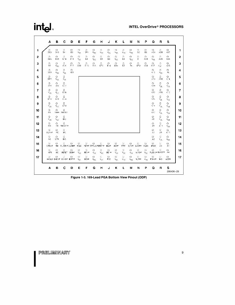
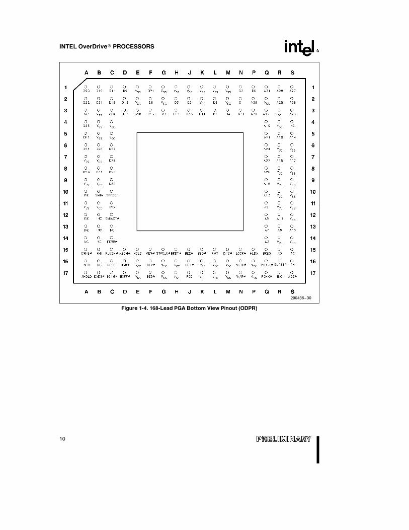
Refer to Figures 1-3 and 1-4 for an illustration ofeach of the two PGA packages. Figure 1-3 showsthe 169-lead PGA package, while Figure 1-4 illus-trates the 168-lead PGA package.
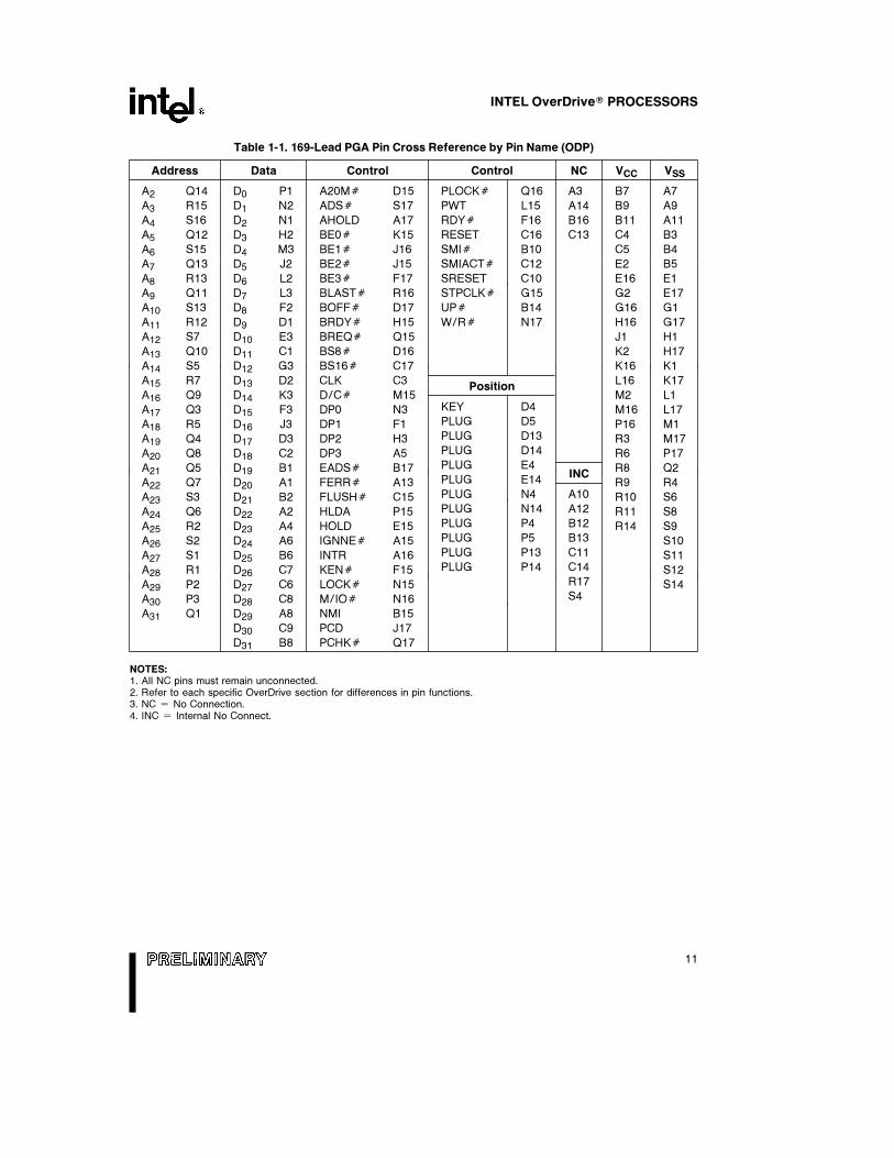
Table 1-1 cross-references the pin number to pinfunction for the 169-lead PGA package. Table 1-2 isa cross-reference for the 168-lead package.
Table 5-1 in Section 5 gives a brief description of thefunction of each pin.
Refer to each specific OverDrive processor sectionfor a description of any differences from the pinoutsdescribed in this section.
8
INTEL OverDriveÉ PROCESSORS
290436–29
Figure 1-3. 169-Lead PGA Bottom View Pinout (ODP)
9
INTEL OverDriveÉ PROCESSORS
290436–30
Figure 1-4. 168-Lead PGA Bottom View Pinout (ODPR)
10
INTEL OverDriveÉ PROCESSORS
Table 1-1. 169-Lead PGA Pin Cross Reference by Pin Name (ODP)
Address Data Control Control NC VCC VSS
A2 Q14 D0 P1 A20MÝ D15 PLOCKÝ Q16 A3 B7 A7
A3 R15 D1 N2 ADSÝ S17 PWT L15 A14 B9 A9
A4 S16 D2 N1 AHOLD A17 RDYÝ F16 B16 B11 A11
A5 Q12 D3 H2 BE0Ý K15 RESET C16 C13 C4 B3
A6 S15 D4 M3 BE1Ý J16 SMIÝ B10 C5 B4
A7 Q13 D5 J2 BE2Ý J15 SMIACTÝ C12 E2 B5
A8 R13 D6 L2 BE3Ý F17 SRESET C10 E16 E1
A9 Q11 D7 L3 BLASTÝ R16 STPCLKÝ G15 G2 E17
A10 S13 D8 F2 BOFFÝ D17 UPÝ B14 G16 G1
A11 R12 D9 D1 BRDYÝ H15 W/RÝ N17 H16 G17
A12 S7 D10 E3 BREQÝ Q15 J1 H1
A13 Q10 D11 C1 BS8Ý D16 K2 H17
A14 S5 D12 G3 BS16Ý C17 K16 K1
A15 R7 D13 D2 CLK C3 L16 K17Position
A16 Q9 D14 K3 D/CÝ M15 M2 L1KEY D4A17 Q3 D15 F3 DP0 N3 M16 L17PLUG D5A18 R5 D16 J3 DP1 F1 P16 M1PLUG D13A19 Q4 D17 D3 DP2 H3 R3 M17PLUG D14A20 Q8 D18 C2 DP3 A5 R6 P17PLUG E4A21 Q5 D19 B1 EADSÝ B17 R8 Q2
INCPLUG E14A22 Q7 D20 A1 FERRÝ A13 R9 R4PLUG N4 A10A23 S3 D21 B2 FLUSHÝ C15 R10 S6PLUG N14 A12A24 Q6 D22 A2 HLDA P15 R11 S8PLUG P4 B12A25 R2 D23 A4 HOLD E15 R14 S9PLUG P5 B13A26 S2 D24 A6 IGNNEÝ A15 S10PLUG P13 C11A27 S1 D25 B6 INTR A16 S11PLUG P14 C14A28 R1 D26 C7 KENÝ F15 S12
R17A29 P2 D27 C6 LOCKÝ N15 S14S4A30 P3 D28 C8 M/IOÝ N16
A31 Q1 D29 A8 NMI B15
D30 C9 PCD J17
D31 B8 PCHKÝ Q17
NOTES:1. All NC pins must remain unconnected.2. Refer to each specific OverDrive section for differences in pin functions.3. NC e No Connection.4. INC e Internal No Connect.
11
INTEL OverDriveÉ PROCESSORS
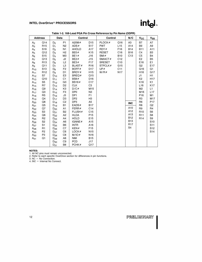
Table 1-2. 168-Lead PGA Pin Cross Reference by Pin Name (ODPR)
Address Data Control Control N/C VCC VSS
A2 Q14 D0 P1 A20MÝ D15 PLOCKÝ Q16 A3 B7 A7
A3 R15 D1 N2 ADSÝ S17 PWT L15 A14 B9 A9
A4 S16 D2 N1 AHOLD A17 RDYÝ F16 B14 B11 A11
A5 Q12 D3 H2 BE0Ý K15 RESET C16 B16 C4 B3
A6 S15 D4 M3 BE1Ý J16 SMIÝ B10 C13 C5 B4
A7 Q13 D5 J2 BE2Ý J15 SMIACTÝ C12 E2 B5
A8 R13 D6 L2 BE3Ý F17 SRESET C10 E16 E1
A9 Q11 D7 L3 BLASTÝ R16 STPCLKÝ G15 G2 E17
A10 S13 D8 F2 BOFFÝ D17 UPÝ C11 G16 G1
A11 R12 D9 D1 BRDYÝ H15 W/RÝ N17 H16 G17
A12 S7 D10 E3 BREQÝ Q15 J1 H1
A13 Q10 D11 C1 BS8Ý D16 K2 H17
A14 S5 D12 G3 BS16Ý C17 K16 K1
A15 R7 D13 D2 CLK C3 L16 K17
A16 Q9 D14 K3 D/CÝ M15 M2 L1
A17 Q3 D15 F3 DP0 N3 M16 L17
A18 R5 D16 J3 DP1 F1 P16 M1
A19 Q4 D17 D3 DP2 H3 R3 M17
A20 Q8 D18 C2 DP3 A5 R6 P17INC
A21 Q5 D19 B1 EADSÝ B17 R8 Q2A10A22 Q7 D20 A1 FERRÝ C14 R9 R4A12A23 S3 D21 B2 FLUSHÝ C15 R10 S6A13A24 Q6 D22 A2 HLDA P15 R11 S8B12A25 R2 D23 A4 HOLD E15 R14 S9B13A26 S2 D24 A6 IGNNEÝ A15 S10R17A27 S1 D25 B6 INTR A16 S11S4A28 R1 D26 C7 KENÝ F15 S12
A29 P2 D27 C6 LOCKÝ N15 S14
A30 P3 D28 C8 M/IOÝ N16
A31 Q1 D29 A8 NMI B15
D30 C9 PCD J17
D31 B8 PCHKÝ Q17
NOTES:1. All NC pins must remain unconnected.2. Refer to each specific OverDrive section for differences in pin functions.3. NC e No Connection.4. INC e Internal No Connect.
12
INTEL OverDriveÉ PROCESSORS
1.2.2 PentiumÉ OverDriveÉ PROCESSORSPECIFICATIONS
The Intel Pentium OverDrive processor socket spec-ifies 237 contacts. The 237 contacts correspond to astandard 240 pin socket with one inside ‘‘KEY’’ con-tact, one outer ‘‘KEY’’ contact and four ’orientation’contacts plugged on the outside corner. The inside‘‘KEY’’ contact provides backward compatibility forthe IntelDX2 and IntelDX4 OverDrive processors forIntel486 SX, Intel486 DX, IntelSX2, and IntelDX2processor-based systems. The Pentium OverDriveprocessor itself (not the socket) does not have any
‘‘KEY’’ pins. The five contacts plugged on the out-side corner ensure proper orientation for the Penti-um OverDrive processor. The Pentium OverDriveprocessor pinout is shown in Figures 1-5 and 1-6.
Please note that the boundary scan pins (TCK,TDO,TDI, and TMS), and all testability pins havebeen removed from the production version of thePentium OverDrive processor. An engineering sam-ple will be available that will allow the use of bounda-ry scan and testability functions. For more informa-tion on boundary scan and testability pins, pleasecontact Intel.
13
INTEL OverDriveÉ PROCESSORS
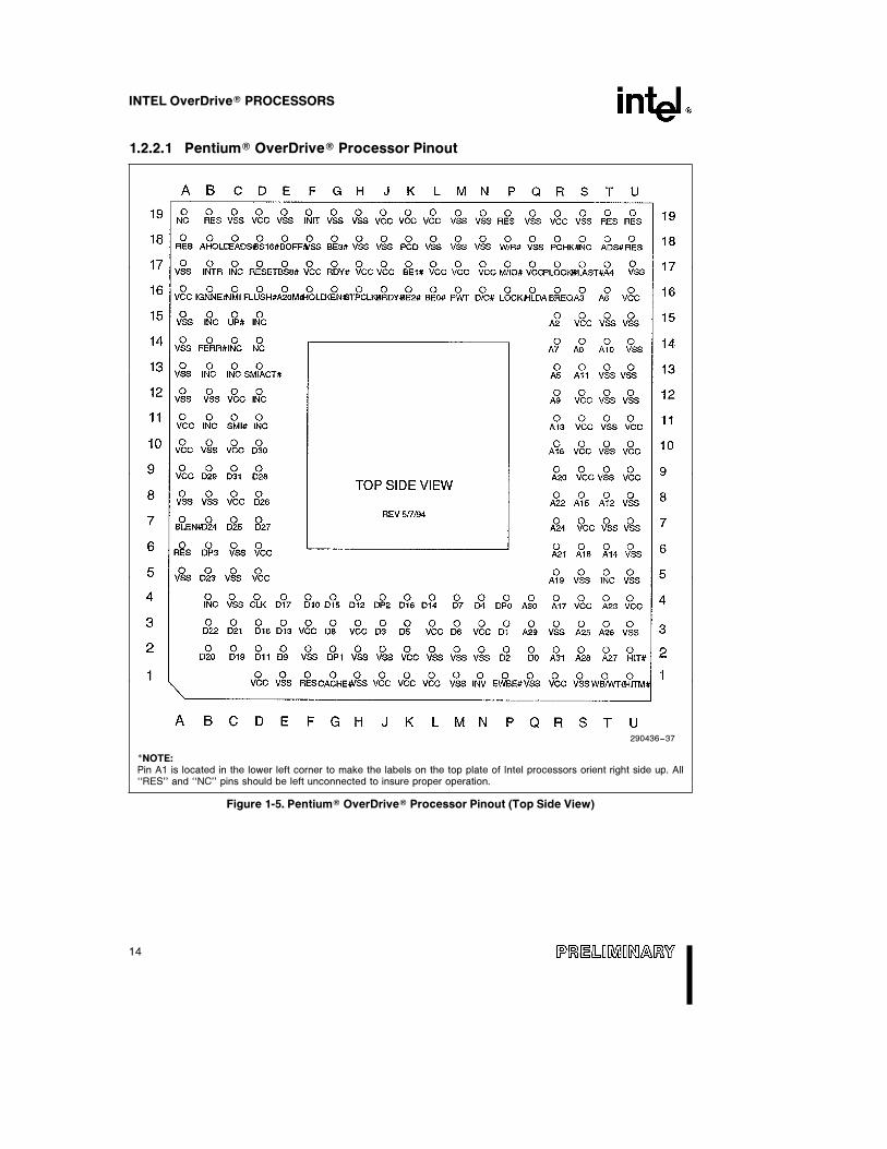
1.2.2.1 PentiumÉ OverDriveÉ Processor Pinout
290436–37
*NOTE:Pin A1 is located in the lower left corner to make the labels on the top plate of Intel processors orient right side up. All‘‘RES’’ and ‘‘NC’’ pins should be left unconnected to insure proper operation.
Figure 1-5. PentiumÉ OverDriveÉ Processor Pinout (Top Side View)
14
INTEL OverDriveÉ PROCESSORS
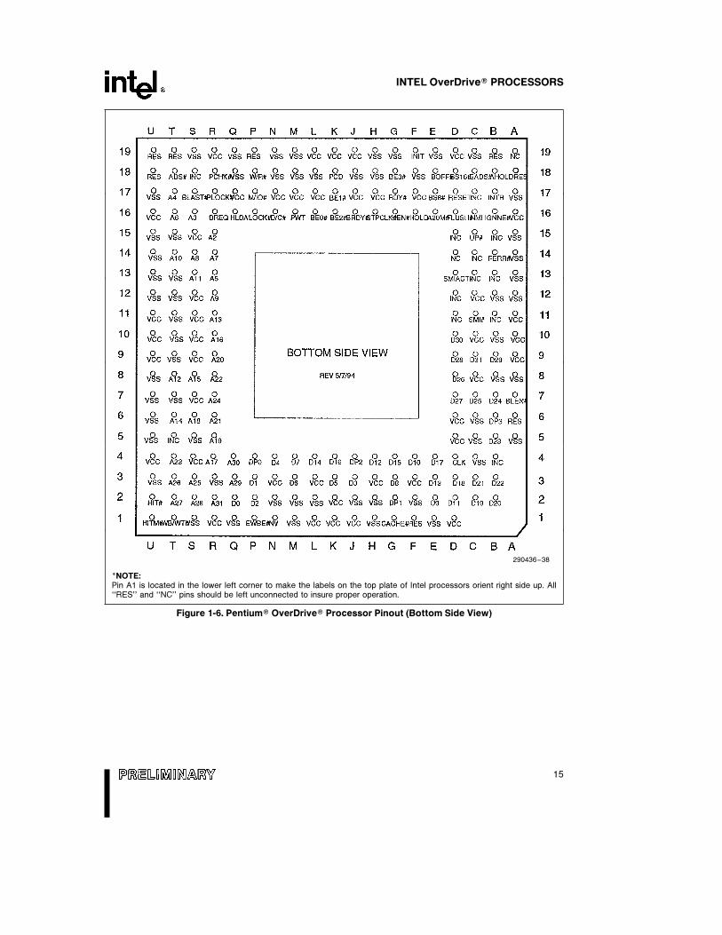
290436–38
*NOTE:Pin A1 is located in the lower left corner to make the labels on the top plate of Intel processors orient right side up. All‘‘RES’’ and ‘‘NC’’ pins should be left unconnected to insure proper operation.
Figure 1-6. PentiumÉ OverDriveÉ Processor Pinout (Bottom Side View)
15
INTEL OverDriveÉ PROCESSORS
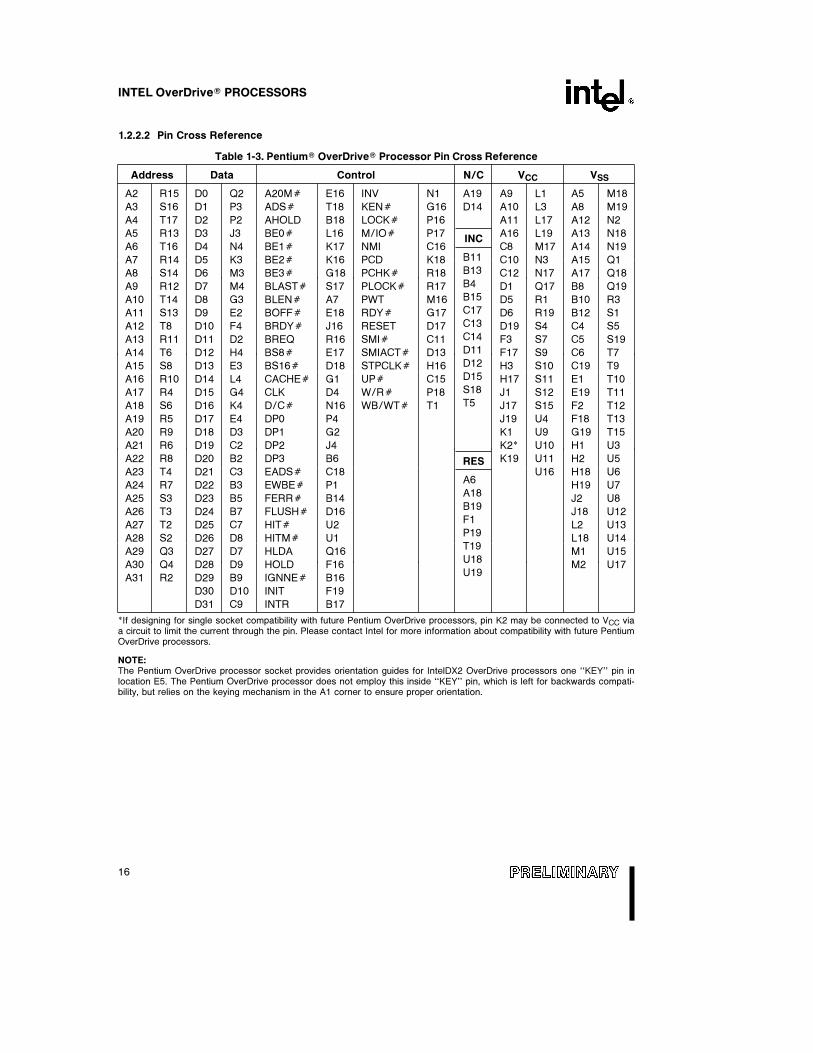
1.2.2.2 Pin Cross Reference
Table 1-3. PentiumÉ OverDriveÉ Processor Pin Cross Reference
Address Data Control N/C VCC VSS
A2 R15 D0 Q2 A20MÝ E16 INV N1 A19 A9 L1 A5 M18
A3 S16 D1 P3 ADSÝ T18 KENÝ G16 D14 A10 L3 A8 M19
A4 T17 D2 P2 AHOLD B18 LOCKÝ P16 A11 L17 A12 N2
A5 R13 D3 J3 BE0Ý L16 M/IOÝ P17 A16 L19 A13 N18INC
A6 T16 D4 N4 BE1Ý K17 NMI C16 C8 M17 A14 N19B11A7 R14 D5 K3 BE2Ý K16 PCD K18 C10 N3 A15 Q1B13A8 S14 D6 M3 BE3Ý G18 PCHKÝ R18 C12 N17 A17 Q18B4A9 R12 D7 M4 BLASTÝ S17 PLOCKÝ R17 D1 Q17 B8 Q19B15A10 T14 D8 G3 BLENÝ A7 PWT M16 D5 R1 B10 R3C17A11 S13 D9 E2 BOFFÝ E18 RDYÝ G17 D6 R19 B12 S1C13A12 T8 D10 F4 BRDYÝ J16 RESET D17 D19 S4 C4 S5C14A13 R11 D11 D2 BREQ R16 SMIÝ C11 F3 S7 C5 S19D11A14 T6 D12 H4 BS8Ý E17 SMIACTÝ D13 F17 S9 C6 T7D12A15 S8 D13 E3 BS16Ý D18 STPCLKÝ H16 H3 S10 C19 T9D15A16 R10 D14 L4 CACHEÝ G1 UPÝ C15 H17 S11 E1 T10S18A17 R4 D15 G4 CLK D4 W/RÝ P18 J1 S12 E19 T11T5A18 S6 D16 K4 D/CÝ N16 WB/WTÝ T1 J17 S15 F2 T12
A19 R5 D17 E4 DP0 P4 J19 U4 F18 T13
A20 R9 D18 D3 DP1 G2 K1 U9 G19 T15
A21 R6 D19 C2 DP2 J4 K2* U10 H1 U3
A22 R8 D20 B2 DP3 B6 K19 U11 H2 U5RESA23 T4 D21 C3 EADSÝ C18 U16 H18 U6
A6A24 R7 D22 B3 EWBEÝ P1 H19 U7
A18A25 S3 D23 B5 FERRÝ B14 J2 U8
B19A26 T3 D24 B7 FLUSHÝ D16 J18 U12
F1A27 T2 D25 C7 HITÝ U2 L2 U13
P19A28 S2 D26 D8 HITMÝ U1 L18 U14
T19A29 Q3 D27 D7 HLDA Q16 M1 U15
U18A30 Q4 D28 D9 HOLD F16 M2 U17
U19A31 R2 D29 B9 IGNNEÝ B16
D30 D10 INIT F19
D31 C9 INTR B17
*If designing for single socket compatibility with future Pentium OverDrive processors, pin K2 may be connected to VCC viaa circuit to limit the current through the pin. Please contact Intel for more information about compatibility with future PentiumOverDrive processors.
NOTE:The Pentium OverDrive processor socket provides orientation guides for IntelDX2 OverDrive processors one ‘‘KEY’’ pin inlocation E5. The Pentium OverDrive processor does not employ this inside ‘‘KEY’’ pin, which is left for backwards compati-bility, but relies on the keying mechanism in the A1 corner to ensure proper orientation.
16
INTEL OverDriveÉ PROCESSORS
2.0 IntelDX2TM OverDriveÉ PROCESSOR FOR Intel486TM SX AND DXMICROPROCESSOR-BASED SYSTEMS
Y Processor Upgrade for most Intel486TM
SX and DX Processor-Based SystemsÐ Single-Chip UpgradeÐ Increases Both Integer and Floating
Point Performance
Y Two Package Variations to SupportSystems with and without anOverDriveÉ Processor Socket
Y 169-Lead Pin Grid Array PackageÐ Pin Compatible with Intel487TM SX
Math CoProcessorÐ 169th Alignment Pin Ensures Proper
Chip Orientation
Y 168-Lead Pin Grid Array PackageÐ Pin Compatible with Intel486TM DX
Processor
Y Utilizes IntelDX2 Speed-DoublingTechnologyÐ Processor Core Runs at Twice the
Frequency of the System BusÐ Compatible with 33, 25, 20 and
16 MHz Systems
Y Floating Point Math Unit Included On-Chip
Y High Integration Enables On-ChipÐ 8 KByte Code and Data CacheÐ Paged, Virtual Memory Management
Y Binary Compatible with Large InstalledSoftware BaseÐ MS-DOS, OS/2TM, WindowsÐ UNIX System V/386Ð IRMX, IRMKTM Kernals
Y High Performance DesignÐ Core Clock Speed up to 66 MHzÐ 106 Mbyte/sec Burst BusÐ CHMOS V Process Technology
Y Complete 32-Bit ArchitectureÐ Address and Data BussesÐ RegistersÐ 8-, 16-, 32-Bit Data Types
Y Compatible with Intel SL EnhancedFeatures
The IntelDX2 OverDrive processor is the entry-level processor upgrade option offering excellent price/per-formance for cost-conscious users of most Intel486 SX and DX processor-based systems. Based on Intel’sIntelDX2 technology, the IntelDX2 OverDrive processor integrates an integer unit, a floating point unit, amemory management unit, SL Enhanced features and an 8 KByte cache on a single chip.
Using the IntelDX2 processor’s speed doubling technology, the IntelDX2 OverDrive processor operates inter-nally at twice the speed of the system bus. This allows users of Intel486 SX and DX microprocessor-basedsystems to double the frequency of their computer’s processor by adding a single chip, without upgrading anyother system components. For example, adding an IntelDX2 OverDrive processor to an Intel486 DX 33 MHzsystem will double the processor’s internal operating speed to 66 MHz.
17
INTEL OverDriveÉ PROCESSORS
The IntelDX2 OverDrive processor is based on theIntelDX2 microprocessor technology. This technolo-gy doubles the clock speed of the internal processorcore, while interfacing with the system at the sameexternal clock speed. When installed in a 33 MHzIntel486 SX or DX microprocessor-based system,the internal processor core, integer unit, floatingpoint unit and cache operate at 66 MHz, while thespeed of the external bus remains at 33 MHz. Thisprovides increased processor performance whilemaintaining compatibility with the existing systemdesign.
The IntelDX2 OverDrive processor is currently avail-able in four product versions, which consist of twospeed options (50 MHz and 66 MHz) and two pack-age options (168-lead Pin Grid Array (PGA) and 169-lead PGA).
The 50 MHz IntelDX2 OverDrive processor is de-signed to upgrade 25 MHz Intel486 DX microproces-
sor-based systems and 16 MHz, 20 MHz and25 MHz Intel486 SX microprocessor-based systems.The 66 MHz IntelDX2 OverDrive processor is de-signed to upgrade 33 MHz Intel486 SX and DXmicroprocessor-based systems. Table 2-1 illustratesthe speed and pinout configurations for each systemtype.
These products come with a (0.25× high) heat sinkattached to the standard 169-lead PGA or 168-leadPGA package to aid in heat dissipation. All IntelDX2OverDrive processors are binary compatible with alarge base of software based on DOS, OS/2, Win-dows and Unix operating systems.
For more detailed information about the operation ofthe IntelDX2 OverDrive processor, refer to the In-telDX2 microprocessor data book (Order Ý241731-001).
18
INTEL OverDriveÉ PROCESSORS
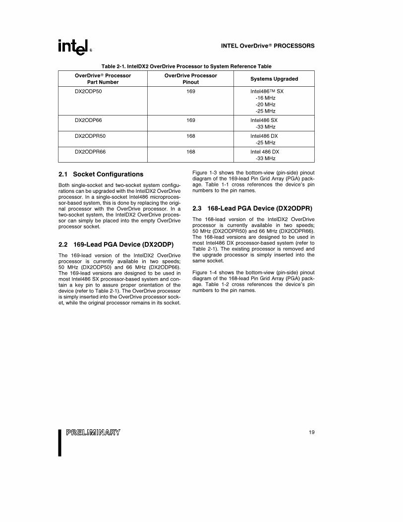
Table 2-1. IntelDX2 OverDrive Processor to System Reference Table
OverDriveÉ Processor OverDrive ProcessorSystems Upgraded
Part Number Pinout
DX2ODP50 169 Intel486TM SX
-16 MHz
-20 MHz
-25 MHz
DX2ODP66 169 Intel486 SX
-33 MHz
DX2ODPR50 168 Intel486 DX
-25 MHz
DX2ODPR66 168 Intel 486 DX
-33 MHz
2.1 Socket Configurations
Both single-socket and two-socket system configu-rations can be upgraded with the IntelDX2 OverDriveprocessor. In a single-socket Intel486 microproces-sor-based system, this is done by replacing the origi-nal processor with the OverDrive processor. In atwo-socket system, the IntelDX2 OverDrive proces-sor can simply be placed into the empty OverDriveprocessor socket.
2.2 169-Lead PGA Device (DX2ODP)
The 169-lead version of the IntelDX2 OverDriveprocessor is currently available in two speeds;50 MHz (DX2ODP50) and 66 MHz (DX2ODP66).The 169-lead versions are designed to be used inmost Intel486 SX processor-based system and con-tain a key pin to assure proper orientation of thedevice (refer to Table 2-1). The OverDrive processoris simply inserted into the OverDrive processor sock-et, while the original processor remains in its socket.
Figure 1-3 shows the bottom-view (pin-side) pinoutdiagram of the 169-lead Pin Grid Array (PGA) pack-age. Table 1-1 cross references the device’s pinnumbers to the pin names.
2.3 168-Lead PGA Device (DX2ODPR)
The 168-lead version of the IntelDX2 OverDriveprocessor is currently available in two speeds;50 MHz (DX2ODPR50) and 66 MHz (DX2ODPR66).The 168-lead versions are designed to be used inmost Intel486 DX processor-based system (refer toTable 2-1). The existing processor is removed andthe upgrade processor is simply inserted into thesame socket.
Figure 1-4 shows the bottom-view (pin-side) pinoutdiagram of the 168-lead Pin Grid Array (PGA) pack-age. Table 1-2 cross references the device’s pinnumbers to the pin names.
19


INTEL OverDriveÉ PROCESSORS
3.0 IntelDX4TM OverDriveÉ PROCESSOR FOR Intel486TM SX AND DXMICROPROCESSOR-BASED SYSTEMS
Y Processor Upgrade for most Intel486TM
SX and DX Processor-Based SystemsÐ Single-Chip UpgradeÐ Increases Both Integer and Floating
Point Performance
Y Two Package Variations to SupportSystems with and without anOverDriveÉ Processor Socket
Y 169-Lead Pin Grid Array PackageÐ Pin Compatible with Intel487TM SX
Math CoProcessorÐ 169th Alignment Pin Ensures Proper
Chip Orientation
Y 168-Lead Pin Grid Array PackageÐ Pin Compatible with Intel486TM DX
Processor
Y High Integration Enables On-ChipÐ 16 KByte Code and Data CacheÐ Paged, Virtual Memory Management
Y Floating Point Math Unit IncludedOn-Chip
Y Utilizes IntelDX4 Speed-TriplingTechnologyÐ Processor Core Runs at Three Times
the Frequency of the System BusÐ Compatible with 33, 25, 20 and
16 MHz Systems
Y Binary Compatible with Large InstalledSoftware and Operating System BaseÐ MS-DOS, OS/2TM, WindowsÐ UNIX System V/386Ð IRMX, IRMKTM Kernals
Y High Performance DesignÐ Core Clock Speed up to 100 MHzÐ CHMOS V Process Technology
Y Complete 32-Bit ArchitectureÐ Address and Data BussesÐ RegistersÐ 8-, 16-, 32-Bit Data Types
Y SL Enhanced Intel486TM
Microprocessor Features IncludedOn-Chip
The IntelDX4 OverDrive processor is an upgrade for most Intel486 SX and DX microprocessor-based systems.It operates at a maximum internal core frequency of 100 MHz and is available in two package versions. Wheninstalled in a system, the IntelDX4 OverDrive processor significantly increases both the integer and floatingpoint performance.
The IntelDX4 OverDrive processor offers several new features not found in the IntelDX2 OverDrive proces-sors. It has 16 KByte on-chip cache and the internal core operates at 3x (speed tripled) the external clockfrequency. The underlying technology behind the IntelDX4 OverDrive processor is the IntelDX4 microproces-sor core with on-package voltage regulation. This allows the OverDrive processor to plug directly into existing5V systems. Like the IntelDX2 OverDrive processor the IntelDX4 OverDrive processor supports System Man-agement Mode (SMM) and Stop Clock Mode. The SMM and Stop Clock Mode, identical to those implementedin SL Enhanced Intel486 SX and DX microprocessors, make the IntelDX4 OverDrive processor compatiblewith the advanced power management, system security and device emulation features of SL Enhanced sys-tems.
21
INTEL OverDriveÉ PROCESSORS
The IntelDX4 OverDrive processor is based on theIntelDX4 microprocessor technology. This technolo-gy triples the clock speed of the internal processorcore, while interfacing with the system at the sameexternal clock speed. When installed in a 33 MHzIntel486 SX or DX microprocessor-based system,the internal processor core, integer unit, floatingpoint unit and cache operate at 100 MHz, while thespeed of the external bus remains at 33 MHz. Thisprovides increased processor performance whilemaintaining compatibility with the existing systemdesign. In addition, the internal cache has been dou-bled to 16 KBytes.
The IntelDX4 OverDrive processor is currently avail-able in four product versions, which consist of twospeed options (75 MHz and 100 MHz) and two pack-age options (168-lead Pin Grid Array (PGA) and 169-lead PGA).
The 100 MHz OverDrive processors are designed toupgrade most 33 MHz Intel486 SX and DX micro-
processor-based systems. The 75 MHz OverDriveprocessors are designed to upgrade most 25 MHzIntel486 DX microprocessor-based systems and16 MHz, 20 MHz and 25 MHz Intel486 SX micro-processor-based systems. Table 3-1 illustrates this.The speed tripling technology will triple the internalspeed of the processor to three times the bus speedof the existing system.
These products come with a (0.6× high) heat sinkattached to the standard 169-lead PGA or 168-leadPGA package to aid in heat dissipation. Refer toSections 14.0 and 15.0 for clearance and thermalrequirements. All IntelDX4 OverDrive processors arebinary compatible with a large base of softwarebased on DOS, OS/2, Windows and Unix operatingsystems.
For more detailed information about the operation ofthe IntelDX4 OverDrive processor, refer to theIntelDX4 microprocessor data book (OrderÝ241944-001).
22
INTEL OverDriveÉ PROCESSORS
Table 3-1. IntelDX4 OverDrive Processor to System Reference Table
OverDriveÉ Processor OverDrive ProcessorSystems Upgraded
Part Number Pinout
DX4ODP75 169 Intel486TM SX
-16 MHz
-20 MHz
-25 MHz
DX4ODP100 169 Intel486 SX
-33 MHz
DX4ODPR75 168 Intel486 DX
-25 MHz
DX4ODPR100 168 Intel 486 DX
-33 MHz
3.1 Socket Configurations
Both single-socket and two-socket system configu-rations can be upgraded with the IntelDX4 OverDriveprocessor. In a single-socket Intel486 microproces-sor-based system, this is done by replacing the origi-nal processor with the OverDrive processor. In atwo-socket system, the IntelDX4 OverDrive proces-sor can simply be placed into the empty OverDriveprocessor socket.
3.2 169-Lead PGA Device (DX4ODP)
The 169-lead version of the IntelDX4 OverDriveprocessor is currently available in two speeds;75 MHz (DX4ODP75) and 100 MHz (DX4ODP100).The 169-lead versions are designed to be used inmost Intel486 SX processor-based system and con-tain a key pin to assure proper orientation of thedevice (refer to Table 3-1). The processor is simplyinserted into the OverDrive processor socket, whilethe original processor remains in its socket.
Figure 1-3 shows the bottom-view (pin-side) pinoutdiagram of the 169-lead Pin Grid Array (PGA) pack-age. Table 1-1 cross references the device’s pinnumbers to the pin names.
3.3 168-Lead PGA Device (DX4ODPR)
The 168-lead version of the IntelDX4 OverDriveprocessor is currently available in two speeds;75 MHz (DX4ODPR75) and 100 MHz(DX4ODPR100). The 168-lead versions are de-signed to be used in most Intel486 DX processor-based system (refer to Table 3-1). The existing proc-essor is removed and the upgrade processor is sim-ply inserted into the same socket.
Figure 1-4 shows the bottom-view (pin-side) pinoutdiagram of the 168-lead Pin Grid Array (PGA) pack-age. Table 1-2 cross references the device’s pinnumbers to the pin names.
23

INTEL OverDriveÉ PROCESSORS
4.0 INTEL PentiumÉ OverDriveÉ PROCESSOR
Y Powerful CPU Upgrade for mostIntel486TM CPU-Based SystemsÐ Makes Intel Procesor-Based Systems
Run FasterÐ Significantly Accelerates All
Software Applications
Y Designed for Systems Based on:Ð Intel486 SX ProcessorsÐ Intel486 DX ProcessorsÐ IntelSX2TM ProcessorsÐ IntelDX2TM Processors
Y Compatible with Installed Base ofThousands of Applications
Y Based on Intel PentiumÉ ProcessorTechnologyÐ Superscalar Architecture
Ð Branch PredictionÐ Faster Floating Point Unit
Y Enhancements to Core PentiumProcessor SiliconÐ Separate Code and Data CachesÐ 16 KB Code CacheÐ 16 KB Write-Back Data CacheÐ 32-Bit Bus Interface
Y Package InnovationsÐ On-Package Voltage RegulationÐ Integrated Fan Heat Sink
Y Incorporates SMM Power SavingFeatures
The Pentium OverDrive processor is Intel’s highest performance CPU upgrade for systems based on theIntel486 family of CPUs. It is the recommended upgrade option for most IntelSX2 and IntelDX2 CPU-basedsystems and the superior upgrade option for most Intel486 SX and DX CPU-based systems. The Pentiumprocessor’s superscalar architecture (which allows more than one instruction per clock cycle to be executed),the 32 KB enhanced on-chip cache memory and faster floating point unit provide a significant performanceboost across a wide range of applications. The specially-designed bus interface unit enables the PentiumOverDrive processor to operate internally at 64 bits while working seamlessly with the 32-bit Intel486 architec-ture.
The Pentium OverDrive processor may contain certain design defects or errors known as errata. Currentcharacterized errata are available on request.
25

INTEL OverDriveÉ PROCESSORS
4.1 Product Description
The Pentium OverDrive processor is designed to up-grade most systems based on Intel486 SX, Intel486DX, IntelSX2, and IntelDX2 processor-based sys-tems and is based on Intel’s Pentium processortechnology. It is 100% binary compatible with the8086/88, 80286, Intel386 DX, Intel386 SX, Intel486DX, Intel486 SX, IntelSX2, and the IntelDX2 proces-sor family.
The Pentium OverDrive processor provides signifi-cant improvements over the Intel486 CPU including:
# Superscalar Architecture
# Dynamic Branch Prediction
# Pipelined Floating-Point Unit
# Separate 16K Code and 16K Data Caches
# Improved Instruction Execution Times
# Write back MESI Protocol implemented in DataCache
# System Management Mode
The Pentium OverDrive processor significantly in-creases the integer performance, and can attain upto 2x floating-point performance relative to an equiv-alent frequency IntelDX2 processor. The bus fre-quencies for the Pentium OverDrive processor are25 MHz and 33 MHz.
The Pentium OverDrive processor has two pipelinesand a floating-point unit that are capable of indepen-dent operation. Each pipeline issues frequently usedinstructions in a single clock. Together, the dualpipes can issue two integer instructions in one clock,or one floating point instruction (under certain cir-cumstances, 2 floating point instructions) in oneclock.
The floating-point unit has been completely rede-signed over the IntelDX2 processor. Faster algo-rithms provide at least 3X internal speed-up for com-mon floating point operations including ADD, MUL,and LOAD. With instruction scheduling and over-lapped (pipelined) execution, these three perform-ance enhancements can allow many math intensiveapplications to achieve a 2X performance boost.
The Pentium OverDrive processor implements 32-bitaddress and data busses.
The Pentium OverDrive processor has separatecode and data caches, both are 16 KBytes each.The data cache has write-back capabilities.
The Pentium OverDrive also has an integrated fanheat sink. The heat sink contains logic circuitrywhich senses if the speed of the fan is insufficient tocool the processor and will reduce the internal fre-quency of the processor to that of the internal bus.This will allow the processor to run indefinitely with-out damage.
NOTE:1. Refer to the Pentium Processor DataBook for more information on instruction ex-ecution timing and pairing.
26
INTEL OverDriveÉ PROCESSORS
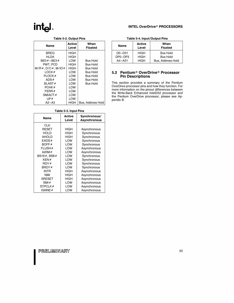
5.0 PIN DESCRIPTIONS
5.1 Pins Common to All OverDriveÉProcessors
Tables 5-1 through 5-4 list pin descriptions of thesignals present on the Intel DX2, IntelDX4 OverDriveprocessors, and are not unique on the PentiumOverDrive processor.
Table 5-1. Pin Descriptions
Symbol Type Name and Function
CLK I Clock provides the fundamental timing for the bus interface unit and is multiplied bytwo (2x) for the IntelDX2 OverDrive Processors or three (3x) for the IntelDX4OverDrive Processor to provide the internal frequency for the Intel OverDriveprocessor. All external timing parameters are specified with respect to the risingedge of CLK.
ADDRESS BUS
A31–A4 I/O A31–A2 are theaddress lines of the processor. A31–A2, together with the byteenables BE0Ý–BE3Ý, define the physical area of memory or input/output spaceA2–A3 Oaccessed. Address lines A31–A4 are used to drive addresses into the processor toperform cache line invalidations. Input signals must meet setup and hold times t22and t23. A31–A2 are not driven during bus or address hold.
BE0–3Ý O Thebyte enable signals indicate active bytes during read and write cycles. Duringthe first cycle of a cache fill, the external system should assume that all byteenables are active. BE3Ý applies to D24–D31, BE2Ý applies to D16–D23, BE1Ýapplies to D8–D15 and BE0Ý applies to D0–D7. BE0Ý–BE3Ý are active LOW andare not driven during bus hold.
DATA BUS
D31–D0 I/O These are thedata lines for the Intel OverDrive processor. Lines D0–D7 define theleast significant byte of the data bus while lines D24–D31 define the mostsignificant byte of the data bus. These signals must meet setup and hold times t22and t23 for proper operation on reads. These pins are driven during the second andsubsequent clocks of write cycles.
DATA PARITY
DP0–DP3 I/O There is onedata parity pin for each byte of the data bus. Data parity is generatedon all write data cycles with the same timing as the data driven by the IntelOverDrive processor. Even parity information must be driven back into themicroprocessor on the data parity pins with the same timing as read information toinsure that the correct parity check status is indicated by the Intel OverDriveprocessor. The signals read on these pins do not affect program execution.
Input signals must meet setup and hold times t22 and t23. DP0–DP3 should beconnected to VCC through a pullup resistor in systems which do not use parity.DP0–DP3 are active HIGH and are driven during the second and subsequent clocksof write cycles.
27
INTEL OverDriveÉ PROCESSORS
Table 5-1. Pin Descriptions (Continued)
Symbol Type Name and Function
DATA PARITY (Continued)
PCHKÝ O Parity Status is driven on the PCHKÝ pin the clock after ready for read operations.The parity status is for data sampled at the end of the previous clock. A parity error isindicated by PCHKÝ being LOW. Parity status is only checked for enabled bytes asindicated by the byte enable and bus size signals. PCHKÝ is valid only in the clockimmediately after read data is returned to the microprocessor. At all other timesPCHKÝ is inactive (HIGH). PCHKÝ is never floated.
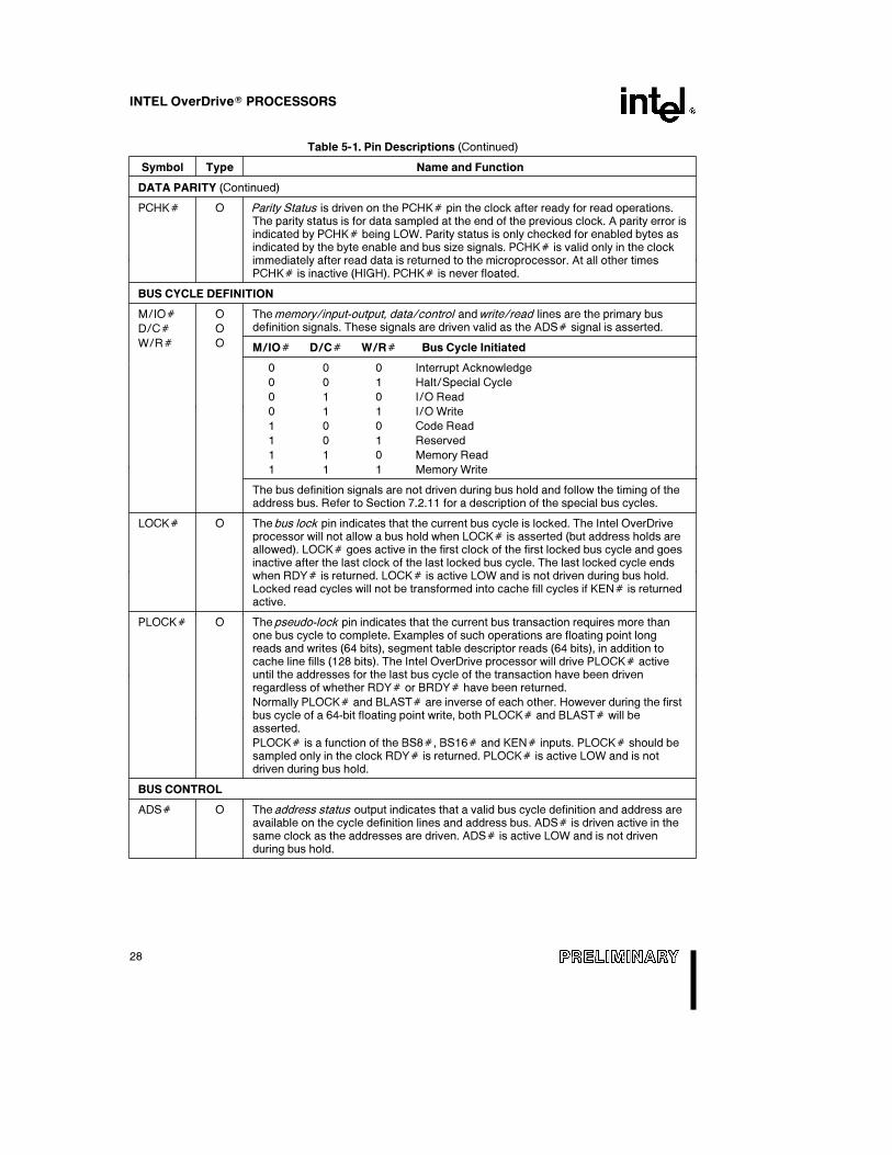
BUS CYCLE DEFINITION
M/IOÝ O Thememory/input-output, data/control andwrite/read lines are the primary busdefinition signals. These signals are driven valid as the ADSÝ signal is asserted.D/CÝ O
W/RÝ O M/IOÝ D/CÝ W/RÝ Bus Cycle Initiated
0 0 0 Interrupt Acknowledge
0 0 1 Halt/Special Cycle
0 1 0 I/O Read
0 1 1 I/O Write
1 0 0 Code Read
1 0 1 Reserved
1 1 0 Memory Read
1 1 1 Memory Write
The bus definition signals are not driven during bus hold and follow the timing of theaddress bus. Refer to Section 7.2.11 for a description of the special bus cycles.
LOCKÝ O Thebus lock pin indicates that the current bus cycle is locked. The Intel OverDriveprocessor will not allow a bus hold when LOCKÝ is asserted (but address holds areallowed). LOCKÝ goes active in the first clock of the first locked bus cycle and goesinactive after the last clock of the last locked bus cycle. The last locked cycle endswhen RDYÝ is returned. LOCKÝ is active LOW and is not driven during bus hold.Locked read cycles will not be transformed into cache fill cycles if KENÝ is returnedactive.
PLOCKÝ O Thepseudo-lock pin indicates that the current bus transaction requires more thanone bus cycle to complete. Examples of such operations are floating point longreads and writes (64 bits), segment table descriptor reads (64 bits), in addition tocache line fills (128 bits). The Intel OverDrive processor will drive PLOCKÝ activeuntil the addresses for the last bus cycle of the transaction have been drivenregardless of whether RDYÝ or BRDYÝ have been returned.
Normally PLOCKÝ and BLASTÝ are inverse of each other. However during the firstbus cycle of a 64-bit floating point write, both PLOCKÝ and BLASTÝ will beasserted.
PLOCKÝ is a function of the BS8Ý, BS16Ý and KENÝ inputs. PLOCKÝ should besampled only in the clock RDYÝ is returned. PLOCKÝ is active LOW and is notdriven during bus hold.
BUS CONTROL
ADSÝ O Theaddress status output indicates that a valid bus cycle definition and address areavailable on the cycle definition lines and address bus. ADSÝ is driven active in thesame clock as the addresses are driven. ADSÝ is active LOW and is not drivenduring bus hold.
28

INTEL OverDriveÉ PROCESSORS
Table 5-1. Pin Descriptions (Continued)
Symbol Type Name and Function
BUS CONTROL (Continued)
RDYÝ I Thenon-burst ready input indicates that the current bus cycle is complete. RDYÝindicates that the external system has presented valid data on the data pins in responseto a read or that the external system has accepted data from the Intel OverDriveprocessor in response to a write. RDYÝ is ignored when the bus is idle and at the end ofthe first clock of the bus cycle.
RDYÝ is active during address hold. Data can be returned to the processor whileAHOLD is active.
RDYÝ is active LOW, and is not provided with an internal pullup resistor. RDYÝ mustsatisfy setup and hold times t16 and t17 for proper chip operation.
BURST CONTROL
BRDYÝ I Theburst ready input performs the same function during a burst cycle that RDYÝperforms during a non-burst cycle. BRDYÝ indicates that the external system haspresented valid data in response to a read or that the external system has accepted datain response to a write. BRDYÝ is ignored when the bus is idle and at the end of the firstclock in a bus cycle.
BRDYÝ is sampled in the second and subsequent clocks of a burst cycle. The datapresented on the data bus will be strobed into the microprocessor when BRDYÝ issampled active. If RDYÝ is returned simultaneously with BRDYÝ, BRDYÝ is ignoredand the burst cycle is prematurely interrupted
BRDYÝ is active LOW and is provided with a small pullup resistor. BRDYÝ must satisfythe setup and hold times t16 and t17.
BLASTÝ O Theburst last signal indicates that the next time BRDYÝ is returned the burst bus cycleis complete. BLASTÝ is active for both burst and non-burst bus cycles. BLASTÝ isactive LOW and is not driven during bus hold.
INTERRUPTS
RESET I The RESET input forces the processor to begin execution at a known state. Reset isasynchronous, but must meet setup and hold times t20 and t21 for recognition in anyspecific clock. The processor cannot begin execution of instructions until at least 1 msafter VCC and CLK have reached their proper AC and DC specifications. However, forsoft resets, RESET should remain active for at least 15 CLK periods. The RESET pinshould remain active during this time to ensure proper processor operation. RESET isactive HIGH.
RESET sets the SMBASE descriptor to a default address of 30000H. If the system usesSMBASE relocation, then the SRESET pin should be used for soft resets.
SRESET I The SRESET pin duplicates all the functionality of the RESET pin with the following twoexceptions:
1. The SMBASE register will retain its previous value.
2. If UPÝ (I) is asserted, SRESET will not have an effect on the host microprocessor.
For soft resets, SRESET should remain active for at least 15 CLK periods. SRESET isactive HIGH. SRESET is asynchronous but must meet setup and hold times t20 and t21for recognition in any specific clock.
29
INTEL OverDriveÉ PROCESSORS
Table 5-1. Pin Descriptions (Continued)
Symbol Type Name and Function
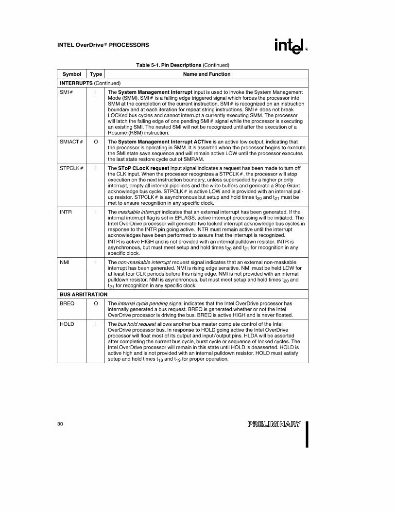
INTERRUPTS (Continued)
SMIÝ I The System Management Interrupt input is used to invoke the System ManagementMode (SMM). SMIÝ is a falling edge triggered signal which forces the processor intoSMM at the completion of the current instruction. SMIÝ is recognized on an instructionboundary and at each iteration for repeat string instructions. SMIÝ does not breakLOCKed bus cycles and cannot interrupt a currently executing SMM. The processorwill latch the falling edge of one pending SMIÝ signal while the processor is executingan existing SMI. The nested SMI will not be recognized until after the execution of aResume (RSM) instruction.
SMIACTÝ O The System Management Interrupt ACTive is an active low output, indicating thatthe processor is operating in SMM. It is asserted when the processor begins to executethe SMI state save sequence and will remain active LOW until the processor executesthe last state restore cycle out of SMRAM.
STPCLKÝ I The SToP CLocK request input signal indicates a request has been made to turn offthe CLK input. When the processor recognizes a STPCLKÝ, the processor will stopexecution on the next instruction boundary, unless superseded by a higher priorityinterrupt, empty all internal pipelines and the write buffers and generate a Stop Grantacknowledge bus cycle. STPCLKÝ is active LOW and is provided with an internal pull-up resistor. STPCLKÝ is asynchronous but setup and hold times t20 and t21 must bemet to ensure recognition in any specific clock.
INTR I Themaskable interrupt indicates that an external interrupt has been generated. If theinternal interrupt flag is set in EFLAGS, active interrupt processing will be initiated. TheIntel OverDrive processor will generate two locked interrupt acknowledge bus cycles inresponse to the INTR pin going active. INTR must remain active until the interruptacknowledges have been performed to assure that the interrupt is recognized.
INTR is active HIGH and is not provided with an internal pulldown resistor. INTR isasynchronous, but must meet setup and hold times t20 and t21 for recognition in anyspecific clock.
NMI I Thenon-maskable interrupt request signal indicates that an external non-maskableinterrupt has been generated. NMI is rising edge sensitive. NMI must be held LOW forat least four CLK periods before this rising edge. NMI is not provided with an internalpulldown resistor. NMI is asynchronous, but must meet setup and hold times t20 andt21 for recognition in any specific clock.
BUS ARBITRATION
BREQ O The internal cycle pending signal indicates that the Intel OverDrive processor hasinternally generated a bus request. BREQ is generated whether or not the IntelOverDrive processor is driving the bus. BREQ is active HIGH and is never floated.
HOLD I Thebus hold request allows another bus master complete control of the IntelOverDrive processor bus. In response to HOLD going active the Intel OverDriveprocessor will float most of its output and input/output pins. HLDA will be assertedafter completing the current bus cycle, burst cycle or sequence of locked cycles. TheIntel OverDrive processor will remain in this state until HOLD is deasserted. HOLD isactive high and is not provided with an internal pulldown resistor. HOLD must satisfysetup and hold times t18 and t19 for proper operation.
30
INTEL OverDriveÉ PROCESSORS
Table 5-1. Pin Descriptions (Continued)
Symbol Type Name and Function
BUS ARBITRATION (Continued)
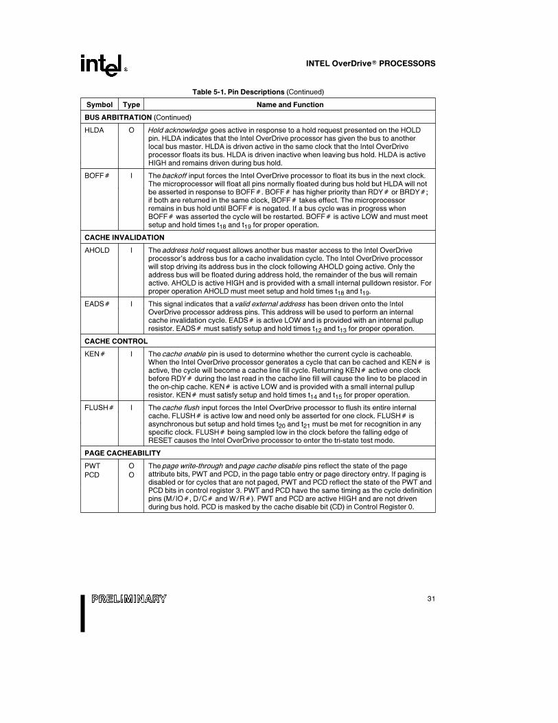
HLDA O Hold acknowledge goes active in response to a hold request presented on the HOLDpin. HLDA indicates that the Intel OverDrive processor has given the bus to anotherlocal bus master. HLDA is driven active in the same clock that the Intel OverDriveprocessor floats its bus. HLDA is driven inactive when leaving bus hold. HLDA is activeHIGH and remains driven during bus hold.
BOFFÝ I Thebackoff input forces the Intel OverDrive processor to float its bus in the next clock.The microprocessor will float all pins normally floated during bus hold but HLDA will notbe asserted in response to BOFFÝ. BOFFÝ has higher priority than RDYÝ or BRDYÝ;if both are returned in the same clock, BOFFÝ takes effect. The microprocessorremains in bus hold until BOFFÝ is negated. If a bus cycle was in progress whenBOFFÝ was asserted the cycle will be restarted. BOFFÝ is active LOW and must meetsetup and hold times t18 and t19 for proper operation.
CACHE INVALIDATION
AHOLD I Theaddress hold request allows another bus master access to the Intel OverDriveprocessor’s address bus for a cache invalidation cycle. The Intel OverDrive processorwill stop driving its address bus in the clock following AHOLD going active. Only theaddress bus will be floated during address hold, the remainder of the bus will remainactive. AHOLD is active HIGH and is provided with a small internal pulldown resistor. Forproper operation AHOLD must meet setup and hold times t18 and t19.
EADSÝ I This signal indicates that avalid external address has been driven onto the IntelOverDrive processor address pins. This address will be used to perform an internalcache invalidation cycle. EADSÝ is active LOW and is provided with an internal pullupresistor. EADSÝ must satisfy setup and hold times t12 and t13 for proper operation.
CACHE CONTROL
KENÝ I Thecache enable pin is used to determine whether the current cycle is cacheable.When the Intel OverDrive processor generates a cycle that can be cached and KENÝ isactive, the cycle will become a cache line fill cycle. Returning KENÝ active one clockbefore RDYÝ during the last read in the cache line fill will cause the line to be placed inthe on-chip cache. KENÝ is active LOW and is provided with a small internal pullupresistor. KENÝ must satisfy setup and hold times t14 and t15 for proper operation.
FLUSHÝ I Thecache flush input forces the Intel OverDrive processor to flush its entire internalcache. FLUSHÝ is active low and need only be asserted for one clock. FLUSHÝ isasynchronous but setup and hold times t20 and t21 must be met for recognition in anyspecific clock. FLUSHÝ being sampled low in the clock before the falling edge ofRESET causes the Intel OverDrive processor to enter the tri-state test mode.
PAGE CACHEABILITY
PWT O Thepage write-through andpage cache disable pins reflect the state of the pageattribute bits, PWT and PCD, in the page table entry or page directory entry. If paging isPCD Odisabled or for cycles that are not paged, PWT and PCD reflect the state of the PWT andPCD bits in control register 3. PWT and PCD have the same timing as the cycle definitionpins (M/IOÝ, D/CÝ and W/RÝ). PWT and PCD are active HIGH and are not drivenduring bus hold. PCD is masked by the cache disable bit (CD) in Control Register 0.
31
INTEL OverDriveÉ PROCESSORS
Table 5-1. Pin Descriptions (Continued)
Symbol Type Name and Function
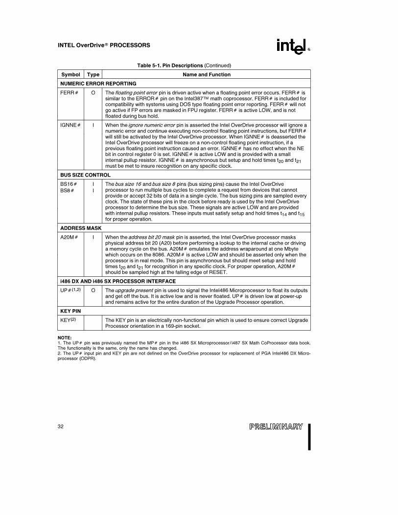
NUMERIC ERROR REPORTING
FERRÝ O The floating point error pin is driven active when a floating point error occurs. FERRÝ issimilar to the ERRORÝ pin on the Intel387TM math coprocessor. FERRÝ is included forcompatibility with systems using DOS type floating point error reporting. FERRÝ will notgo active if FP errors are masked in FPU register. FERRÝ is active LOW, and is notfloated during bus hold.
IGNNEÝ I When the ignore numeric error pin is asserted the Intel OverDrive processor will ignore anumeric error and continue executing non-control floating point instructions, but FERRÝwill still be activated by the Intel OverDrive processor. When IGNNEÝ is deasserted theIntel OverDrive processor will freeze on a non-control floating point instruction, if aprevious floating point instruction caused an error. IGNNEÝ has no effect when the NEbit in control register 0 is set. IGNNEÝ is active LOW and is provided with a smallinternal pullup resistor. IGNNEÝ is asynchronous but setup and hold times t20 and t21must be met to insure recognition on any specific clock.
BUS SIZE CONTROL
BS16Ý I Thebus size 16 andbus size 8 pins (bus sizing pins) cause the Intel OverDriveprocessor to run multiple bus cycles to complete a request from devices that cannotBS8Ý Iprovide or accept 32 bits of data in a single cycle. The bus sizing pins are sampled everyclock. The state of these pins in the clock before ready is used by the Intel OverDriveprocessor to determine the bus size. These signals are active LOW and are providedwith internal pullup resistors. These inputs must satisfy setup and hold times t14 and t15for proper operation.
ADDRESS MASK
A20MÝ I When theaddress bit 20 mask pin is asserted, the Intel OverDrive processor masksphysical address bit 20 (A20) before performing a lookup to the internal cache or drivinga memory cycle on the bus. A20MÝ emulates the address wraparound at one Mbytewhich occurs on the 8086. A20MÝ is active LOW and should be asserted only when theprocessor is in real mode. This pin is asynchronous but should meet setup and holdtimes t20 and t21 for recognition in any specific clock. For proper operation, A20MÝshould be sampled high at the falling edge of RESET.
i486 DX AND i486 SX PROCESSOR INTERFACE
UPÝ(1,2) O Theupgrade present pin is used to signal the Intel486 Microprocessor to float its outputsand get off the bus. It is active low and is never floated. UPÝ is driven low at power-upand remains active for the entire duration of the Upgrade Processor operation.
KEY PIN
KEY(2) The KEY pin is an electrically non-functional pin which is used to ensure correct UpgradeProcessor orientation in a 169-pin socket.
NOTE:1. The UPÝ pin was previously named the MPÝ pin in the i486 SX Microprocessor/i487 SX Math CoProcessor data book.The functionality is the same, only the name has changed.2. The UPÝ input pin and KEY pin are not defined on the OverDrive processor for replacement of PGA Intel486 DX Micro-processor (ODPR).
32
INTEL OverDriveÉ PROCESSORS
Table 5-2. Output Pins
NameActive When
Level Floated
BREQ HIGH
HLDA HIGH
BE0Ý–BE3Ý LOW Bus Hold
PWT, PCD HIGH Bus Hold
W/RÝ, D/CÝ, M/IOÝ HIGH Bus Hold
LOCKÝ LOW Bus Hold
PLOCKÝ LOW Bus Hold
ADSÝ LOW Bus Hold
BLASTÝ LOW Bus Hold
PCHKÝ LOW
FERRÝ LOW
SMIACTÝ LOW
UPÝ LOW
A2–A3 HIGH Bus, Address Hold
Table 5-3. Input Pins
NameActive Synchronous/
Level Asynchronous
CLK
RESET HIGH Asynchronous
HOLD HIGH Synchronous
AHOLD HIGH Synchronous
EADSÝ LOW Synchronous
BOFFÝ LOW Synchronous
FLUSHÝ LOW Asynchronous
A20MÝ LOW Asynchronous
BS16Ý, BS8Ý LOW Synchronous
KENÝ LOW Synchronous
RDYÝ LOW Synchronous
BRDYÝ LOW Synchronous
INTR HIGH Asynchronous
NMI HIGH Asynchronous
SRESET HIGH Asynchronous
SMIÝ LOW Asynchronous
STPCLKÝ LOW Asynchronous
IGNNEÝ LOW Asynchronous
Table 5-4. Input/Output Pins
NameActive When
Level Floated
D0–D31 HIGH Bus Hold
DP0–DP3 HIGH Bus Hold
A4–A31 HIGH Bus, Address Hold
5.2 PentiumÉ OverDriveÉ ProcessorPin Descriptions
This section provides a summary of the PentiumOverDrive processor pins and how they function. Formore information on the pinout differences betweenthe Write-Back Enhanced IntelDX2 processor andthe Pentium OverDrive processor, please see Ap-pendix B.
33
INTEL OverDriveÉ PROCESSORS
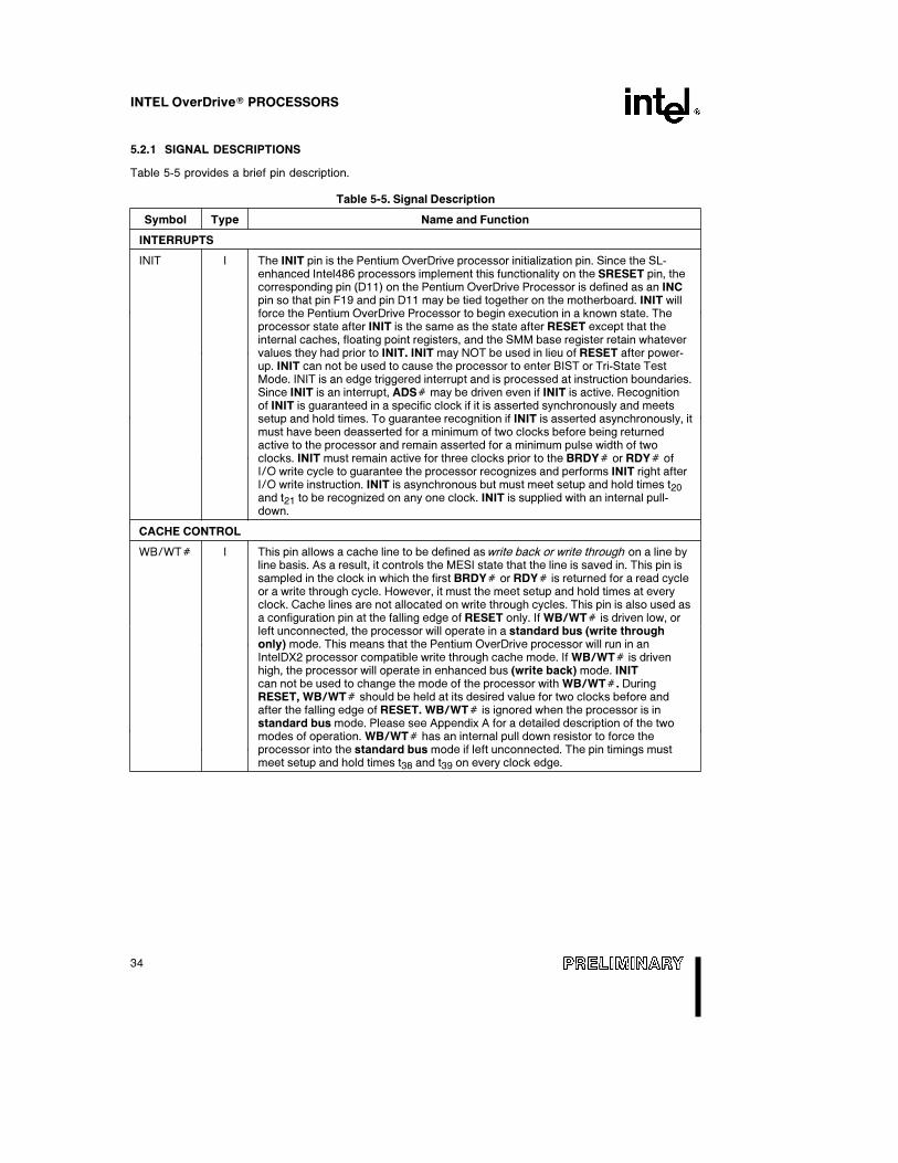
5.2.1 SIGNAL DESCRIPTIONS
Table 5-5 provides a brief pin description.
Table 5-5. Signal Description
Symbol Type Name and Function
INTERRUPTS
INIT I The INIT pin is the Pentium OverDrive processor initialization pin. Since the SL-enhanced Intel486 processors implement this functionality on the SRESET pin, thecorresponding pin (D11) on the Pentium OverDrive Processor is defined as an INCpin so that pin F19 and pin D11 may be tied together on the motherboard. INIT willforce the Pentium OverDrive Processor to begin execution in a known state. Theprocessor state after INIT is the same as the state after RESET except that theinternal caches, floating point registers, and the SMM base register retain whatevervalues they had prior to INIT. INIT may NOT be used in lieu of RESET after power-up. INIT can not be used to cause the processor to enter BIST or Tri-State TestMode. INIT is an edge triggered interrupt and is processed at instruction boundaries.Since INIT is an interrupt, ADSÝ may be driven even if INIT is active. Recognitionof INIT is guaranteed in a specific clock if it is asserted synchronously and meetssetup and hold times. To guarantee recognition if INIT is asserted asynchronously, itmust have been deasserted for a minimum of two clocks before being returnedactive to the processor and remain asserted for a minimum pulse width of twoclocks. INIT must remain active for three clocks prior to the BRDYÝ or RDYÝ ofI/O write cycle to guarantee the processor recognizes and performs INIT right afterI/O write instruction. INIT is asynchronous but must meet setup and hold times t20and t21 to be recognized on any one clock. INIT is supplied with an internal pull-down.
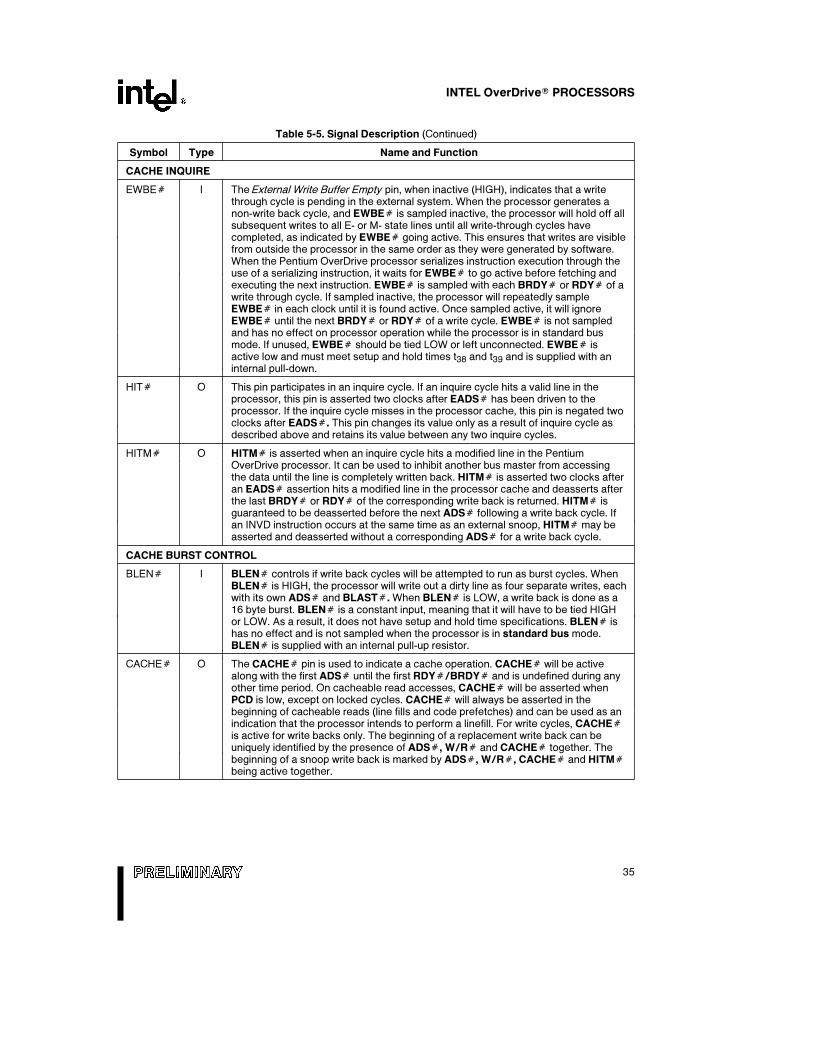
CACHE CONTROL
WB/WTÝ I This pin allows a cache line to be defined aswrite back or write through on a line byline basis. As a result, it controls the MESI state that the line is saved in. This pin issampled in the clock in which the first BRDYÝ or RDYÝ is returned for a read cycleor a write through cycle. However, it must the meet setup and hold times at everyclock. Cache lines are not allocated on write through cycles. This pin is also used asa configuration pin at the falling edge of RESET only. If WB/WTÝ is driven low, orleft unconnected, the processor will operate in a standard bus (write throughonly) mode. This means that the Pentium OverDrive processor will run in anIntelDX2 processor compatible write through cache mode. If WB/WTÝ is drivenhigh, the processor will operate in enhanced bus (write back) mode. INITcan not be used to change the mode of the processor with WB/WTÝ. DuringRESET, WB/WTÝ should be held at its desired value for two clocks before andafter the falling edge of RESET. WB/WTÝ is ignored when the processor is instandard bus mode. Please see Appendix A for a detailed description of the twomodes of operation. WB/WTÝ has an internal pull down resistor to force theprocessor into the standard bus mode if left unconnected. The pin timings mustmeet setup and hold times t38 and t39 on every clock edge.
34
INTEL OverDriveÉ PROCESSORS
Table 5-5. Signal Description (Continued)
Symbol Type Name and Function
CACHE INQUIRE
EWBEÝ I TheExternal Write Buffer Empty pin, when inactive (HIGH), indicates that a writethrough cycle is pending in the external system. When the processor generates anon-write back cycle, and EWBEÝ is sampled inactive, the processor will hold off allsubsequent writes to all E- or M- state lines until all write-through cycles havecompleted, as indicated by EWBEÝ going active. This ensures that writes are visiblefrom outside the processor in the same order as they were generated by software.When the Pentium OverDrive processor serializes instruction execution through theuse of a serializing instruction, it waits for EWBEÝ to go active before fetching andexecuting the next instruction. EWBEÝ is sampled with each BRDYÝ or RDYÝ of awrite through cycle. If sampled inactive, the processor will repeatedly sampleEWBEÝ in each clock until it is found active. Once sampled active, it will ignoreEWBEÝ until the next BRDYÝ or RDYÝ of a write cycle. EWBEÝ is not sampledand has no effect on processor operation while the processor is in standard busmode. If unused, EWBEÝ should be tied LOW or left unconnected. EWBEÝ isactive low and must meet setup and hold times t38 and t39 and is supplied with aninternal pull-down.
HITÝ O This pin participates in an inquire cycle. If an inquire cycle hits a valid line in theprocessor, this pin is asserted two clocks after EADSÝ has been driven to theprocessor. If the inquire cycle misses in the processor cache, this pin is negated twoclocks after EADSÝ. This pin changes its value only as a result of inquire cycle asdescribed above and retains its value between any two inquire cycles.
HITMÝ O HITMÝ is asserted when an inquire cycle hits a modified line in the PentiumOverDrive processor. It can be used to inhibit another bus master from accessingthe data until the line is completely written back. HITMÝ is asserted two clocks afteran EADSÝ assertion hits a modified line in the processor cache and deasserts afterthe last BRDYÝ or RDYÝ of the corresponding write back is returned. HITMÝ isguaranteed to be deasserted before the next ADSÝ following a write back cycle. Ifan INVD instruction occurs at the same time as an external snoop, HITMÝ may beasserted and deasserted without a corresponding ADSÝ for a write back cycle.
CACHE BURST CONTROL
BLENÝ I BLENÝ controls if write back cycles will be attempted to run as burst cycles. WhenBLENÝ is HIGH, the processor will write out a dirty line as four separate writes, eachwith its own ADSÝ and BLASTÝ. When BLENÝ is LOW, a write back is done as a16 byte burst. BLENÝ is a constant input, meaning that it will have to be tied HIGHor LOW. As a result, it does not have setup and hold time specifications. BLENÝ ishas no effect and is not sampled when the processor is in standard bus mode.BLENÝ is supplied with an internal pull-up resistor.
CACHEÝ O The CACHEÝ pin is used to indicate a cache operation. CACHEÝ will be activealong with the first ADSÝ until the first RDYÝ/BRDYÝ and is undefined during anyother time period. On cacheable read accesses, CACHEÝ will be asserted whenPCD is low, except on locked cycles. CACHEÝ will always be asserted in thebeginning of cacheable reads (line fills and code prefetches) and can be used as anindication that the processor intends to perform a linefill. For write cycles, CACHEÝis active for write backs only. The beginning of a replacement write back can beuniquely identified by the presence of ADSÝ, W/RÝ and CACHEÝ together. Thebeginning of a snoop write back is marked by ADSÝ, W/RÝ, CACHEÝ and HITMÝbeing active together.
35
INTEL OverDriveÉ PROCESSORS
Table 5-5. Signal Description (Continued)
Symbol Type Name and Function
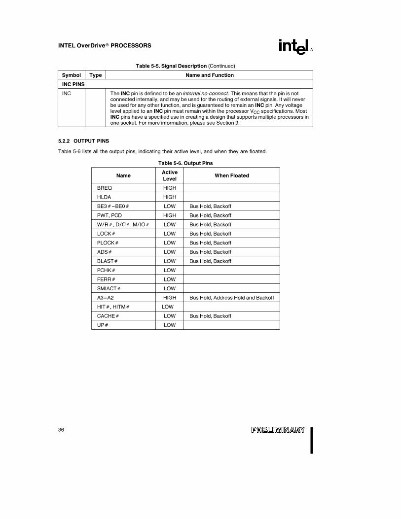
INC PINS
INC The INC pin is defined to be an internal no-connect . This means that the pin is notconnected internally, and may be used for the routing of external signals. It will neverbe used for any other function, and is guaranteed to remain an INC pin. Any voltagelevel applied to an INC pin must remain within the processor VCC specifications. MostINC pins have a specified use in creating a design that supports multiple processors inone socket. For more information, please see Section 9.
5.2.2 OUTPUT PINS
Table 5-6 lists all the output pins, indicating their active level, and when they are floated.
Table 5-6. Output Pins
NameActive
When FloatedLevel
BREQ HIGH
HLDA HIGH
BE3Ý–BE0Ý LOW Bus Hold, Backoff
PWT, PCD HIGH Bus Hold, Backoff
W/RÝ, D/CÝ, M/IOÝ LOW Bus Hold, Backoff
LOCKÝ LOW Bus Hold, Backoff
PLOCKÝ LOW Bus Hold, Backoff
ADSÝ LOW Bus Hold, Backoff
BLASTÝ LOW Bus Hold, Backoff
PCHKÝ LOW
FERRÝ LOW
SMIACTÝ LOW
A3–A2 HIGH Bus Hold, Address Hold and Backoff
HITÝ, HITMÝ LOW
CACHEÝ LOW Bus Hold, Backoff
UPÝ LOW
36
INTEL OverDriveÉ PROCESSORS
5.2.3 INPUT PINS
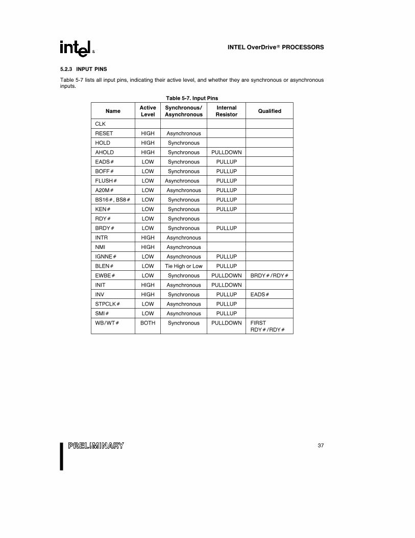
Table 5-7 lists all input pins, indicating their active level, and whether they are synchronous or asynchronousinputs.
Table 5-7. Input Pins
NameActive Synchronous/ Internal
QualifiedLevel Asynchronous Resistor
CLK
RESET HIGH Asynchronous
HOLD HIGH Synchronous
AHOLD HIGH Synchronous PULLDOWN
EADSÝ LOW Synchronous PULLUP
BOFFÝ LOW Synchronous PULLUP
FLUSHÝ LOW Asynchronous PULLUP
A20MÝ LOW Asynchronous PULLUP
BS16Ý, BS8Ý LOW Synchronous PULLUP
KENÝ LOW Synchronous PULLUP
RDYÝ LOW Synchronous
BRDYÝ LOW Synchronous PULLUP
INTR HIGH Asynchronous
NMI HIGH Asynchronous
IGNNEÝ LOW Asynchronous PULLUP
BLENÝ LOW Tie High or Low PULLUP
EWBEÝ LOW Synchronous PULLDOWN BRDYÝ/RDYÝ
INIT HIGH Asynchronous PULLDOWN
INV HIGH Synchronous PULLUP EADSÝ
STPCLKÝ LOW Asynchronous PULLUP
SMIÝ LOW Asynchronous PULLUP
WB/WTÝ BOTH Synchronous PULLDOWN FIRST
RDYÝ/RDYÝ
37
INTEL OverDriveÉ PROCESSORS
5.2.4 INPUT/OUTPUT PINS
Table 5-8 lists all the input/output pins, indicatingtheir active level, and when they are floated.
Table 5-8. Input/Output Pins
NameActive
When FloatedLevel
D31–D0 HIGH Bus Hold, Backoff
DP3–DP0 HIGH Bus Hold, Backoff
A31–A4 HIGH Bus, Address Hold,Backoff
5.3 Architecture Block Diagram
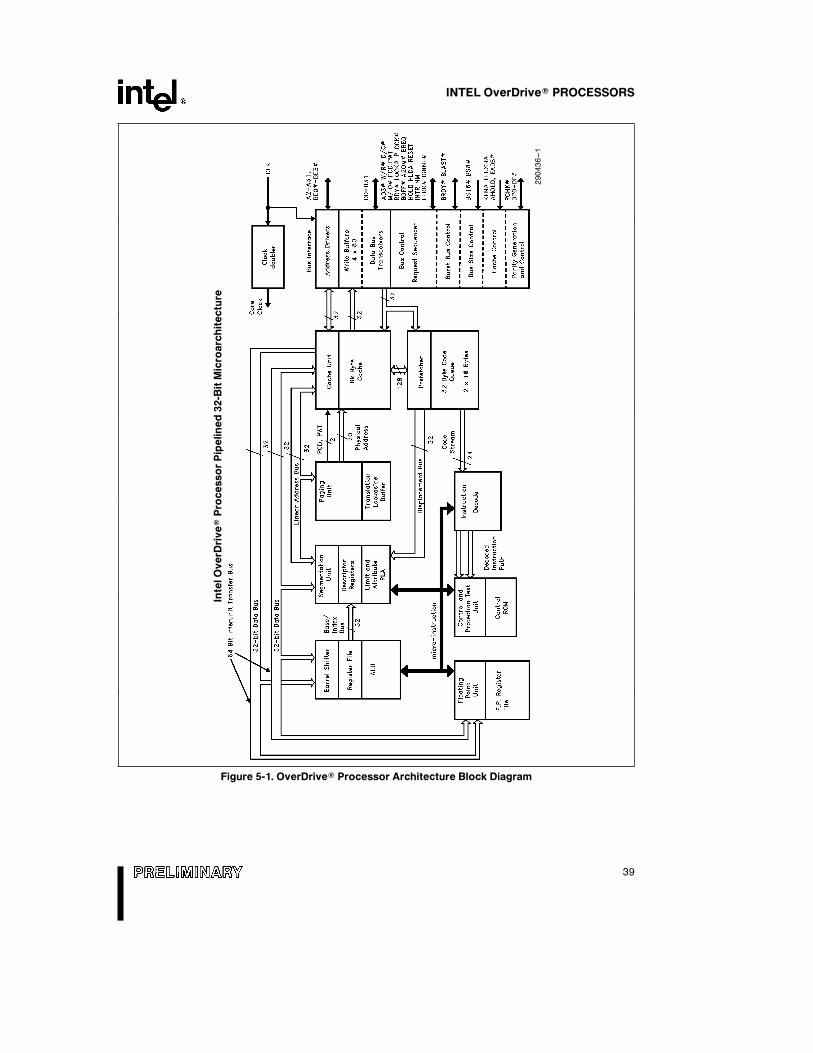
5.3.1 IntelDX2TM AND IntelDX4TM OverDriveÉPROCESSORS
Figure 5-1 shows a block diagram of the IntelDX2and IntelDX4 OverDrive Processor Architecture.There are a few minor architectural differences be-tween each of the OverDrive processors. These dif-ferences are summarized below, with respect to Fig-ure 5-1.
The IntelDX4 OverDrive processor contains a clocktripling circuit, as opposed to the clock doubling cir-cuit used in the IntelDX2 OverDrive processors. Thisis located in the upper left of the diagram.
The IntelDX4 OverDrive processor contains a16 KByte cache, as opposed to the 8 KByte cacheused in the IntelDX2 OverDrive processors. This islocated in the center of the diagram.
38
INTEL OverDriveÉ PROCESSORS
Figure 5-1. OverDriveÉ Processor Architecture Block Diagram
Inte
lO
verD
riveÉ
Pro
cessorPip
elined
32-B
itM
icro
arc
hitectu
re
290436–1
39
INTEL OverDriveÉ PROCESSORS
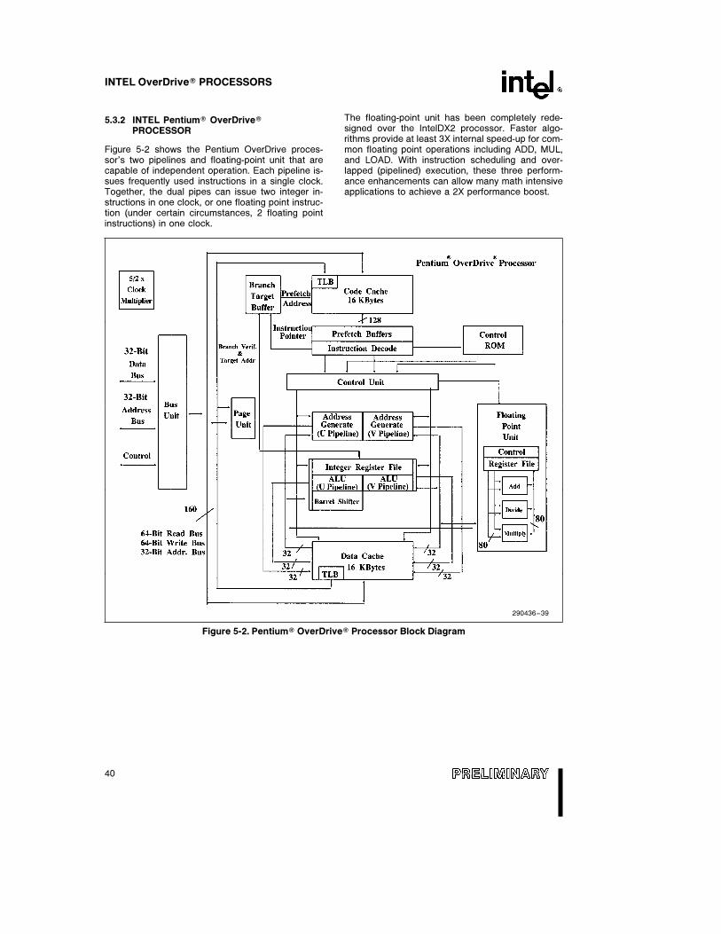
5.3.2 INTEL PentiumÉ OverDriveÉPROCESSOR
Figure 5-2 shows the Pentium OverDrive proces-sor’s two pipelines and floating-point unit that arecapable of independent operation. Each pipeline is-sues frequently used instructions in a single clock.Together, the dual pipes can issue two integer in-structions in one clock, or one floating point instruc-tion (under certain circumstances, 2 floating pointinstructions) in one clock.
The floating-point unit has been completely rede-signed over the IntelDX2 processor. Faster algo-rithms provide at least 3X internal speed-up for com-mon floating point operations including ADD, MUL,and LOAD. With instruction scheduling and over-lapped (pipelined) execution, these three perform-ance enhancements can allow many math intensiveapplications to achieve a 2X performance boost.
290436–39
Figure 5-2. PentiumÉ OverDriveÉ Processor Block Diagram
40
INTEL OverDriveÉ PROCESSORS
The Pentium OverDrive processor implements 32-bitaddress and data busses.
The block diagram shows that the PentiumOverDrive processor contains two instruction pipe-lines, the ‘‘u’’ pipe and the ‘‘v’’ pipe. Both the u- andthe v-pipes execute integer instructions, while onlythe u-pipe executes floating point instructions. Theone exception is the FXCH instruction which mayalso be executed in the v-pipe. Therefore, the Penti-um OverDrive processor is capable of executing twointeger instructions in each clock, or one floatingpoint instruction in each clock. Floating point instruc-tions can be paired in certain conditions(1). Eachpipeline has its own address generation logic, arith-metic logic unit and data cache interface.
NOTE:1. Refer to the Pentium Processor DataBook for more information on instruction ex-ecution timing and pairing.
Note that there are two separate caches, a codecache and a data cache. The data cache has threetag ports, one for each of the two pipes and onededicated to handle snoops from other processors.It has a dedicated Translation Lookaside Buffer(TLB) to translate linear addresses to the physicaladdresses used by the data cache.
The code cache, branch target buffer and prefetchbuffers are responsible for getting raw instructionsinto the execution units of the Pentium OverDriveprocessor. Instructions are fetched from the codecache or from the external bus. Branch addressesare remembered by the branch target buffer. Thecode cache TLB translates linear addresses to phys-ical addresses used by the code cache.
The decode unit decodes the prefetched instruc-tions so that the Pentium OverDrive processor canexecute the instruction. The control ROM containsthe microcode which controls the sequence of oper-ations that must be performed to implement thePentium OverDrive processor architecture. The con-trol ROM unit has direct control over both pipelines.
6.0 DIFFERENCES INFUNCTIONALITY BETWEEN THEIntelDX2TM AND IntelDX4TM
OverDriveÉ PROCESSORFAMILY AND THE Intel486TM SXAND Intel486TM DXPROCESSORS
The IntelDX2 and IntelDX4 OverDrive processorsare an enhanced family of Intel486 microprocessors.There are, however, four functional differences.First, the IntelDX2 and IntelDX4 OverDrive proces-sors have an internal clock doubling (IntelDX2) orclock tripling (IntelDX4) circuit which decreases thetime required to execute instructions. Second, theIntelDX2 and IntelDX4 OverDrive processor familydoes not support the JTAG boundary scan test fea-ture. Third, the IntelDX2 and IntelDX4 OverDriveprocessors have different processor revision identifi-cations than the Intel486 SX or Intel486 DX proces-sors. Finally, the IntelDX4 OverDrive processor con-tains a 16 KByte cache, as opposed to the 8 KBytecache on the IntelDX2 OverDrive processors. Thesefour differences are described in the following sec-tions, according to how they affect the processorfunctionality.
6.1 Hardware Interface
The bus of the Intel OverDrive processors has beendesigned to be identical to the Intel486 Microproces-sor bus. Although the external clock is internallydoubled or tripled, and data and instructions are ma-nipulated in the processor core at twice or threetimes the external frequency, the external bus isfunctionally identical to that of the Intel486 proces-sor.
The four boundary scan test signals (TCK, Testclock; TMS, Test Mode select; TDI, Test Data Input;TDO, Test Data Output), defined for some Intel486processors, are not specified for the Intel486 DX2OverDrive processor.
41
INTEL OverDriveÉ PROCESSORS
The UPÝ (Upgrade Present) signal, which is definedas an input for some Intel486 processors, is an out-put signal on the Intel OverDrive processor. TheUPÝ pin on the Intel OverDrive processor providesa logical low output signal which can be used to en-able logic to recognize and configure the system forthe Intel OverDrive processor. This signal is identicalto the MPÝ output defined for the Intel487 SX MathCoProcessor.
The DX register always contains the componentidentifier at the conclusion of RESET. The IntelOverDrive processor has a different revision identifi-er in the DL register than the Intel486 SX or Intel486DX microprocessors (refer to Section 11.1). Whenthe OverDrive processor is installed in a system thecomponent identifier is supplied by the OverDriveprocessor, rather than the original processor. Thestepping identification portion of the componentidentification will change with different revisions ofthe OverDrive processor. The designer should onlyassume that the component identification for theOverDrive processor will be 043x for the IntelDX2OverDrive processor and 148x or 048x for theIntelDX4 OverDrive processor, where ‘‘x’’ is thestepping identifier.
6.2 Testability
As detailed in Section 6.1, the Intel OverDrive proc-essor does not support the JTAG boundary scantestability feature.
6.3 Instruction Set Summary
The Intel OverDrive processor supports all Intel486extensions to the 8086/80186/80286 instructionset. In general, instructions will run faster on the IntelOverDrive processors than on the Intel486 micro-processor. Specifically, an instruction that only usesmemory from the on-chip cache executes at the fullcore clock rate while all bus accesses execute at thebus clock rate. To calculate the elapsed time of aninstruction, the number of clock counts for that in-struction must be multiplied by the clock period forthe system. The instruction set clock count summarytables from the Intel486 SX and Intel486 DX Micro-
processor Data Sheets can be used for the Over-Drive processor with the following modifications:
Ð Clock counts for a cache hit: This value repre-sents the number of internal processor coreclocks for an instruction that requires no externalbus accesses or the base core clocks for an in-struction requiring external bus accesses.
Ð Penalty clock counts for a cache miss: This valuerepresents the worst-case approximation of theadditional number of external clock counts thatare required for an instruction which must accessthe external bus for data (a cache miss). Thisnumber must be multiplied by 2 (for the IntelSX2and IntelDX2 OverDrive processors) or 3 (for theIntelDX4 OverDrive processor) to convert it to anequal number of internal processor core clockcounts and added to the base core clocks tocompute the number of core clocks for this in-struction.
The actual number of core clocks for an instructionwith a cache miss may be less than the base clockcounts (from the cache hit column) plus the penaltyclock counts (2 times the cache miss column num-ber for the IntelSX2 and IntelDX2, 3 times the cachemiss column number for the IntelDX4). The clockcounts in the cache miss penalty column can be acumulative value of external bus clocks (for datareads) and internal clocks for manipulating the datawhich has been loaded from the external bus. Thenumber of clocks which are related to external busaccesses are correctly represented in terms of inter-nal core clocks by multiplying by two. However, theclock counts related to internal data manipulationshould not be multiplied by two. Therefore the totalnumber of processor core clock counts for an in-struction with a cache miss represents a worst-caseapproximation.
To calculate the execution time for an OverDriveprocessor instruction, multiply the total processorcore clock counts by the core clock period. For ex-ample, in a 25 MHz system upgraded with a 50 MHzIntelDX2 OverDrive processor, the core clock periodis 20 ns (1/50 MHz).
Additionally, the assumptions specified belowshould be understood in order to estimate instruc-tion execution time.
42
INTEL OverDriveÉ PROCESSORS
A cache miss will force the OverDrive processor torun an external bus cycle. The Intel486 microproces-sor 32-bit burst bus is defined as rbbbw.
Where:
r e The number of bus clocks in the first cycle of aburst read or the number of clocks per datacycle is a non-burst read.
b e The number of bus clocks for the second andsubsequent cycles in a burst read.
w e The number of bus clocks for a write.
The fastest bus the OverDrive processor can sup-port is 2b1b2 assuming 0 waits states. The clockcounts in the cache miss penalty column assume a2b1b2 bus. For slower busses add rb2 clocks tothe cache miss penalty for the first dword accessed.Other factors also affect instruction clock counts.
Instruction Clock Count Assumptions
1. The external bus is available for reads or writesat all times. Else add bus clocks to reads untilthe bus is available
2. Accesses are aligned. Add three core clocks toeach misaligned access.
3. Cache fills complete before subsequent access-es to the same line. If a read misses the cacheduring a cache fill due to a previous read or pre-fetch, the read must wait for the cache fill tocomplete. If a read or write accesses a cacheline still being filled, it must wait for the fill tocomplete.
4. If an effective address is calculated, the baseregister is not the destination register of the pre-ceding instruction. If the base register is the des-tination register of the preceding instruction add1 to the core clock counts shown. Back-to-backPUSH and POP instructions are not affected bythis rule.
5. An effective address calculation uses one baseregister and does not use an index register.However, if the effective address calculationuses an index register. 1 core clock may be add-ed to the clock shown.
6. The target of a jump is in the cache. If not, add rclocks for accessing the destination instructionof a jump. If the destination instruction is notcompletely contained in the first dword read, adda maximum of 3b bus clocks. If the destinationinstruction is not completely contained in the first16 byte burst, add a maximum of another ra3bbus clocks.
7. If no write buffer delay, w bus clocks are addedonly in the case in which all write buffers are full.
8. Displacement and immediate not used together.If displacement and immediate used together, 1core clock may be added to the core clock countshown.
9. No invalidate cycles. Add a delay of 1 bus clockfor each invalidate cycle if the invalidate cyclecontends for the internal cache/external buswhen the OverDrive processor needs to use it.
10. Page translation hits in TLB. A TLB miss will add13, 21 or 28 bus clocks a 1 possible core clockto the instruction depending on whether the Ac-cessed and/or Dirty bit in neither, one or both ofthe page entries needs to be set in memory. Thisassumes that neither page entry is in the datacache and a page fault does not occur on theaddress translation.
11. No exceptions are detected during instructionexecution. Refer to interrupt core Clock CountsTable for extra clocks if an interrupt is detected.
12. Instructions that read multiple consecutive dataitems (i.e., task switch, POPA, etc.) and miss thecache are assumed to start the first access on a16-byte boundary. If not, an extra cache line fillmay be necessary which may add up to (ra3b)bus clocks to the cache miss penalty.
7.0 DIFFERENCES BETWEEN THEIntel486TM FAMILY AND THEPentiumÉ OverDriveÉPROCESSOR
This section covers the differences between theIntel486 family of microprocessors and the PentiumOverDrive processor.
7.1 Software
The Pentium OverDrive processor is compatible withthe entire installed base of applications forMS-DOS*, Windows*, OS/2*, and UNIX*. In addi-tion to being binary compatible with the Intel archi-tecture based processors which preceded the Penti-um processor, it can also run programs which havebeen compiled to utilize Pentium processor instruc-tions. This allows pairing of instructions to take ad-vantage of the Superscalar Architecture and addsfloating point instructions if replacing an Intel486 SXor IntelSX2 processor.
43
INTEL OverDriveÉ PROCESSORS
7.2 Hardware
The Pentium OverDrive processor is in a 235-PinGrid Array package while the Intel486 family uses a168-Pin Grid Array package. These extra pins areused for extra power and ground pins, including sep-arate power and ground for the fan heatsink, alsothe internal cache write-back signals are on thesepins.
8.0 DIFFERENCES BETWEEN THEPentiumÉ PROCESSOR ANDTHE PentiumÉ OverDriveÉPROCESSOR
There are several differences between the Pentiumprocessor and the Pentium OverDrive processors.These differences are covered in the next two sec-tions.
8.1 Software
The following paragraphs are provided as a refer-ence for software differences between the PentiumOverDrive processor and the Pentium processor.Unless otherwise stated, it can be assumed that thePentium OverDrive processor will have the samesoftware characteristics as the Pentium processor.For more information on the software characteristicsof the Pentium Processor, please see the PentiumProcessor Data Book or Programmers ReferenceManual .
The Pentium OverDrive processor does not supportmachine check exception. As a result, CR4.MCE isnot useful. It will be forced to a zero by the hard-ware. However, any attempt by the software to setthis bit to 1 will not create a general protection ex-ception.
The Pentium OverDrive processor allows two differ-ent page sizes: 4 KB and 4 MB. Please contact Intelfor more information on the use of 4 MB pages.
The behavior of INVD, WBINVD and INVPLG in-structions are similar to the Pentium processor. If theprocessor is in the enhanced bus mode, theWBINVD instruction will write back all dirty lines first,flush the cache and run two special cycles (the writeback special cycle followed by the flush special cy-cle) on the bus. INVD will flush the cache and runone special cycle (The flush special cycle) on the
bus. INVD will not write back the dirty lines, if any. Allthree instructions are privileged level 0 and shouldbe executed by BIOS or operating system code only.
On the IntelDX2 processor, when paging is disabled,and/or when instructions that are not affected bypaging are executed, the PCD and PWT pins aredriven with values from CR3.PCD and CR3.PWTbits, respectively. On the Pentium OverDrive proces-sor, when paging is disabled and/or when instruc-tions that are not affected by paging are executed,the PWT pin will be drive LOW and the PCD pin willreflect the value of the CR0.CD bit.
When the CPUID instruction is performed with EAXe 1, the Pentium OverDrive processor will returnthe following values to the EDX register. These bitsindicate what features the processor has.
The various bit positions have the following mean-ing:
Table 8-1. Feature Bit Assignment
Bit Value Meaning
0 1 FPU: Floating Point UnitOn-Chip
1 1 VME: Virtual-8086 ModeEnhancements
2 1 DE: Debugging Extensions
3 1 PSE: Page Size Extension
4 1 TSC: Time Stamp Counter
5 1 MSR: Pentium
Processor-Style MSR
6 R Reserved
7 R Reserved
8 1 CX8: CMPXCHG8BInstruction
9–31 R Reserved
A value of ‘‘R’’ means that the corresponding bit isreserved and the software should not depend on itsvalue.
8.2 Hardware
This section covers the hardware differences be-tween the Pentium processor and the Pentium Over-Drive processor.
44
INTEL OverDriveÉ PROCESSORS
The Pentium processor has a 64-bit data bus whilethe Pentium OverDrive processor has a 32-bit databus. This is required in order for the Pentium Over-Drive processor to work in an Intel486 architecturebased system.
The size of the data bus requires a similar decreasein the internal cache line size. A burst memory ac-cess is four bus widths of data this is the length ofeach line in the cache. For an Intel486 based archi-tecture system that is 16-Bytes, for a Pentium proc-essor based system this is 32-bytes. The internalcache in the Pentium processor is expecting32-bytes. This would require two burst reads. There-fore the cache line size was reduced to 16-byteswide.
The cache on the Pentium processor is split into two8 KByte caches. One is for data and the other is theinstruction or code cache. The Pentium OverDriveprocessor keeps the idea of two separate cachesbut increases the size to 16 KBytes each.
The Pentium OverDrive processor does not have theJTAG boundry scan capabilities that the Pentiumprocessor has.
The package is different. The Pentium processor ispackaged in a 273-Pin Grid Array while the PentiumOverDrive processor uses a 235-Pin Grid Arraypackage.
The Pentium OverDrive processor has the integrat-ed fan heatsink attached. This integrated fan in-forms the processor if the fan has slowed orstopped. This reduces the internal frequency to 1xmultiplier from the previous 2.5x. The part can runindefinitely at the lower frequency without incurringany damage. This allows the Pentium OverDriveprocessor to continue in the system until a replace-ment fan can be installed.
9.0 IntelDX2TM AND IntelDX4TM
OverDriveÉ PROCESSORCIRCUIT DESIGN
9.1 Upgrade Circuit for Intel486TM
Processor-Based Systems withUPÝ
Figure 9-1 shows the IntelDX2 and IntelDX4 Over-Drive processor socket circuit for Intel486 proces-sor-based systems using UPÝ. The Upgrade Pres-ent input, UPÝ pin, allows the Intel486 processor todirectly recognize when the Intel OverDrive proces-sor socket is populated. When the UPÝ pin is drivenactive to the Intel486 processor, the Intel486 proc-essor tri-states all of its output pins and enters pow-er-down mode.
45
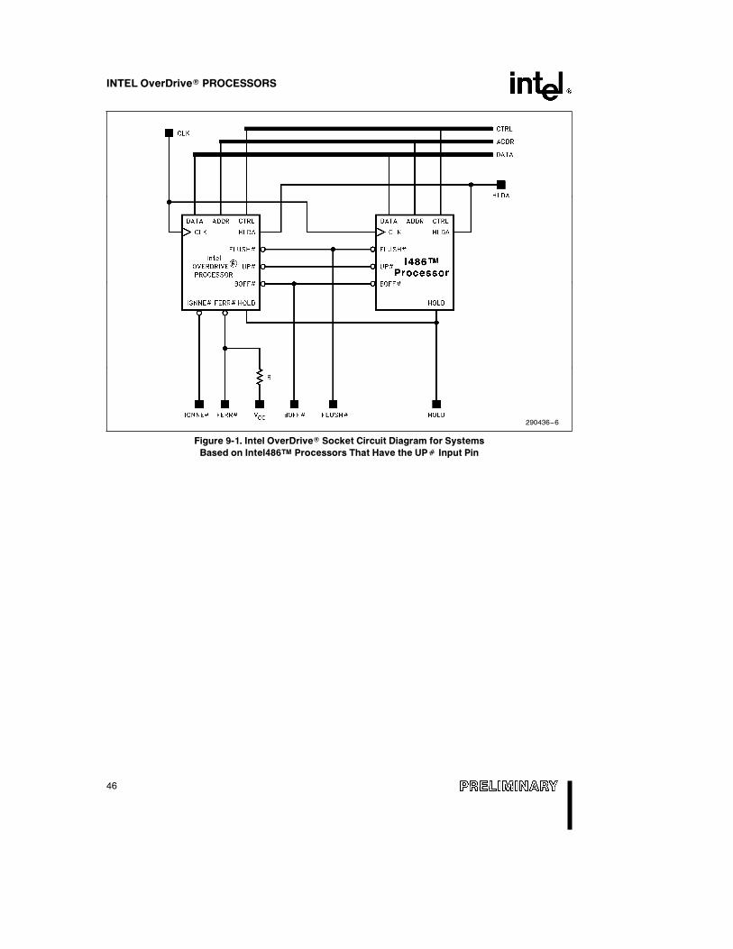
INTEL OverDriveÉ PROCESSORS
290436–6
Figure 9-1. Intel OverDriveÉ Socket Circuit Diagram for Systems
Based on Intel486TM Processors That Have the UPÝ Input Pin
46
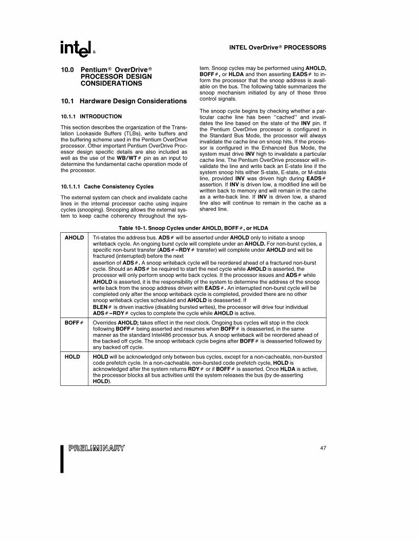
INTEL OverDriveÉ PROCESSORS
10.0 PentiumÉ OverDriveÉPROCESSOR DESIGNCONSIDERATIONS
10.1 Hardware Design Considerations
10.1.1 INTRODUCTION
This section describes the organization of the Trans-lation Lookaside Buffers (TLBs), write buffers andthe buffering scheme used in the Pentium OverDriveprocessor. Other important Pentium OverDrive Proc-essor design specific details are also included aswell as the use of the WB/WTÝ pin as an input todetermine the fundamental cache operation mode ofthe processor.
10.1.1.1 Cache Consistency Cycles
The external system can check and invalidate cachelines in the internal processor cache using inquirecycles (snooping). Snooping allows the external sys-tem to keep cache coherency throughout the sys-
tem. Snoop cycles may be performed using AHOLD,BOFFÝ, or HLDA and then asserting EADSÝ to in-form the processor that the snoop address is avail-able on the bus. The following table summarizes thesnoop mechanism initiated by any of these threecontrol signals.
The snoop cycle begins by checking whether a par-ticular cache line has been ‘‘cached’’ and invali-dates the line based on the state of the INV pin. Ifthe Pentium OverDrive processor is configured inthe Standard Bus Mode, the processor will alwaysinvalidate the cache line on snoop hits. If the proces-sor is configured in the Enhanced Bus Mode, thesystem must drive INV high to invalidate a particularcache line. The Pentium OverDrive processor will in-validate the line and write back an E-state line if thesystem snoop hits either S-state, E-state, or M-stateline, provided INV was driven high during EADSÝassertion. If INV is driven low, a modified line will bewritten back to memory and will remain in the cacheas a write-back line. If INV is driven low, a sharedline also will continue to remain in the cache as ashared line.
Table 10-1. Snoop Cycles under AHOLD, BOFFÝ, or HLDA
AHOLD Tri-states the address bus. ADSÝ will be asserted under AHOLD only to initiate a snoopwriteback cycle. An ongoing burst cycle will complete under an AHOLD. For non-burst cycles, aspecific non-burst transfer (ADSÝ–RDYÝ transfer) will complete under AHOLD and will befractured (interrupted) before the next
assertion of ADSÝ. A snoop writeback cycle will be reordered ahead of a fractured non-burstcycle. Should an ADSÝ be required to start the next cycle while AHOLD is asserted, theprocessor will only perform snoop write back cycles. If the processor issues and ADSÝ while
AHOLD is asserted, it is the responsibility of the system to determine the address of the snoopwrite back from the snoop address driven with EADSÝ. An interrupted non-burst cycle will becompleted only after the snoop writeback cycle is completed, provided there are no othersnoop writeback cycles scheduled and AHOLD is deasserted. If
BLENÝ is driven inactive (disabling bursted writes), the processor will drive four individualADSÝ–RDYÝ cycles to complete the cycle while AHOLD is active.
BOFFÝ Overrides AHOLD; takes effect in the next clock. Ongoing bus cycles will stop in the clockfollowing BOFFÝ being asserted and resumes when BOFFÝ is deasserted, in the samemanner as the standard Intel486 processor bus. A snoop writeback will be reordered ahead ofthe backed off cycle. The snoop writeback cycle begins after BOFFÝ is deasserted followed byany backed off cycle.
HOLD HOLD will be acknowledged only between bus cycles, except for a non-cacheable, non-burstedcode prefetch cycle. In a non-cacheable, non-bursted code prefetch cycle, HOLD isacknowledged after the system returns RDYÝ or if BOFFÝ is asserted. Once HLDA is active,the processor blocks all bus activities until the system releases the bus (by de-assertingHOLD).
47
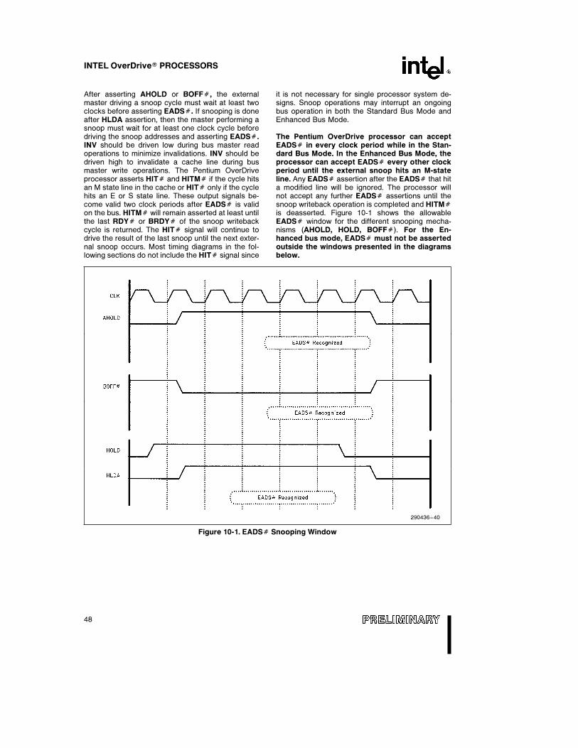
INTEL OverDriveÉ PROCESSORS
After asserting AHOLD or BOFFÝ, the externalmaster driving a snoop cycle must wait at least twoclocks before asserting EADSÝ. If snooping is doneafter HLDA assertion, then the master performing asnoop must wait for at least one clock cycle beforedriving the snoop addresses and asserting EADSÝ.INV should be driven low during bus master readoperations to minimize invalidations. INV should bedriven high to invalidate a cache line during busmaster write operations. The Pentium OverDriveprocessor asserts HITÝ and HITMÝ if the cycle hitsan M state line in the cache or HITÝ only if the cyclehits an E or S state line. These output signals be-come valid two clock periods after EADSÝ is validon the bus. HITMÝ will remain asserted at least untilthe last RDYÝ or BRDYÝ of the snoop writebackcycle is returned. The HITÝ signal will continue todrive the result of the last snoop until the next exter-nal snoop occurs. Most timing diagrams in the fol-lowing sections do not include the HITÝ signal since
it is not necessary for single processor system de-signs. Snoop operations may interrupt an ongoingbus operation in both the Standard Bus Mode andEnhanced Bus Mode.
The Pentium OverDrive processor can acceptEADSÝ in every clock period while in the Stan-dard Bus Mode. In the Enhanced Bus Mode, theprocessor can accept EADSÝ every other clockperiod until the external snoop hits an M-stateline. Any EADSÝ assertion after the EADSÝ that hita modified line will be ignored. The processor willnot accept any further EADSÝ assertions until thesnoop writeback operation is completed and HITMÝis deasserted. Figure 10-1 shows the allowableEADSÝ window for the different snooping mecha-nisms (AHOLD, HOLD, BOFFÝ). For the En-hanced bus mode, EADSÝ must not be assertedoutside the windows presented in the diagramsbelow.
290436–40
Figure 10-1. EADSÝ Snooping Window
48
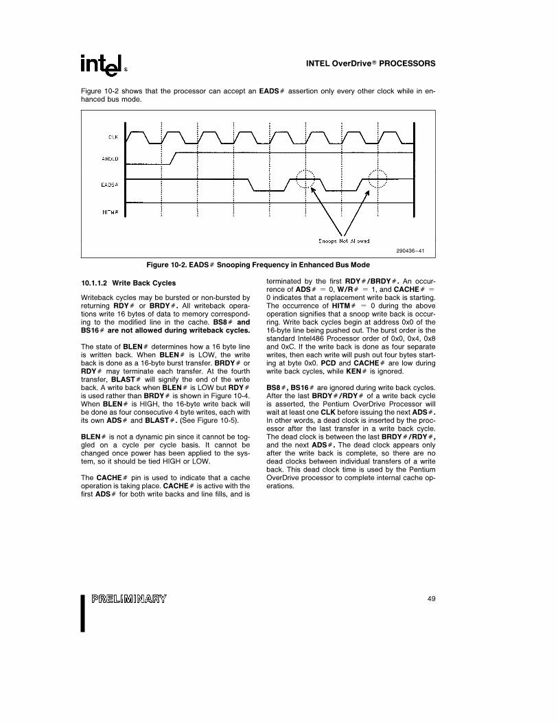
INTEL OverDriveÉ PROCESSORS
Figure 10-2 shows that the processor can accept an EADSÝ assertion only every other clock while in en-hanced bus mode.
290436–41
Figure 10-2. EADSÝ Snooping Frequency in Enhanced Bus Mode
10.1.1.2 Write Back Cycles
Writeback cycles may be bursted or non-bursted byreturning RDYÝ or BRDYÝ. All writeback opera-tions write 16 bytes of data to memory correspond-ing to the modified line in the cache. BS8Ý andBS16Ý are not allowed during writeback cycles.
The state of BLENÝ determines how a 16 byte lineis written back. When BLENÝ is LOW, the writeback is done as a 16-byte burst transfer. BRDYÝ orRDYÝ may terminate each transfer. At the fourthtransfer, BLASTÝ will signify the end of the writeback. A write back when BLENÝ is LOW but RDYÝis used rather than BRDYÝ is shown in Figure 10-4.When BLENÝ is HIGH, the 16-byte write back willbe done as four consecutive 4 byte writes, each withits own ADSÝ and BLASTÝ. (See Figure 10-5).
BLENÝ is not a dynamic pin since it cannot be tog-gled on a cycle per cycle basis. It cannot bechanged once power has been applied to the sys-tem, so it should be tied HIGH or LOW.
The CACHEÝ pin is used to indicate that a cacheoperation is taking place. CACHEÝ is active with thefirst ADSÝ for both write backs and line fills, and is
terminated by the first RDYÝ/BRDYÝ. An occur-rence of ADSÝ e 0, W/RÝ e 1, and CACHEÝ e
0 indicates that a replacement write back is starting.The occurrence of HITMÝ e 0 during the aboveoperation signifies that a snoop write back is occur-ring. Write back cycles begin at address 0x0 of the16-byte line being pushed out. The burst order is thestandard Intel486 Processor order of 0x0, 0x4, 0x8and 0xC. If the write back is done as four separatewrites, then each write will push out four bytes start-ing at byte 0x0. PCD and CACHEÝ are low duringwrite back cycles, while KENÝ is ignored.
BS8Ý, BS16Ý are ignored during write back cycles.After the last BRDYÝ/RDYÝ of a write back cycleis asserted, the Pentium OverDrive Processor willwait at least one CLK before issuing the next ADSÝ.In other words, a dead clock is inserted by the proc-essor after the last transfer in a write back cycle.The dead clock is between the last BRDYÝ/RDYÝ,and the next ADSÝ. The dead clock appears onlyafter the write back is complete, so there are nodead clocks between individual transfers of a writeback. This dead clock time is used by the PentiumOverDrive processor to complete internal cache op-erations.
49
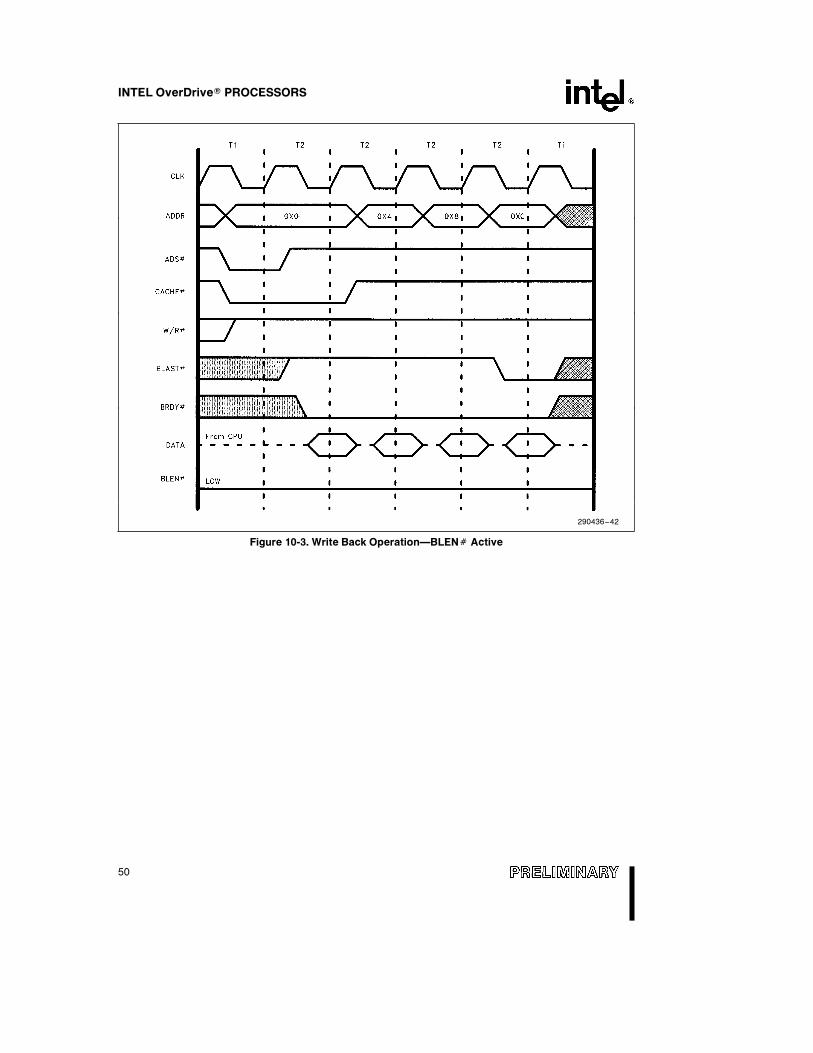
INTEL OverDriveÉ PROCESSORS
290436–42
Figure 10-3. Write Back OperationÐBLENÝ Active
50
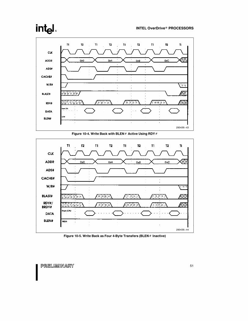
INTEL OverDriveÉ PROCESSORS
290436–43
Figure 10-4. Write Back with BLENÝ Active Using RDYÝ
290436–44
Figure 10-5. Write Back as Four 4-Byte Transfers (BLENÝ Inactive)
51
INTEL OverDriveÉ PROCESSORS
10.1.2 WB/WTÝ AS AN INITIALIZATION INPUT
To make the Pentium OverDrive processor morecompatible with the IntelDX2 processor, severalsmall enhancements have been added to the proc-essor to help distinguish different processor modesof operation. These two modes will be referred to as‘‘standard bus mode’’ (Write through processorcache only) and ‘‘enhanced bus mode’’ (Write backprocessor enabled and are discussed in the follow-ing paragraphs.
In order to allow the Pentium OverDrive processor tooperate in more of an IntelDX2 processor manner,the WB/WTÝ pin is used as an initialization input toconfigure the operating mode of the processor. Atthe falling edge of RESET, the processor can beconfigured to operate in a write through only (In-telDX2 CPU compatible) L1 cache mode (standardbus mode), or in a write back L1 cache mode (en-hanced bus mode). Once a mode is selected, theprocessor will continue to operate in the selectedmode and can only be changed to a different modeby starting the RESET process again. Assertion ofINIT will not change the operating mode of the proc-essor. WB/WTÝ has an internal pulldown that willforce any design that leaves WB/WTÝ unconnect-ed into the write through mode of operation. Table10-2 lists the two modes of operation and the differ-ences between them.
For more information on the effect of the mode op-eration on the various signals mentioned above,please see the Intel486 Microprocessor Family DataBook. Unless otherwise mentioned, all other func-tions of the Pentium OverDrive processor remainidentical in both operating modes.
10.1.3 INIT FUNCTIONALITY
INIT behaves like an edge triggered interrupt on thePentium OverDrive processor while in both en-hanced bus mode (WB/WTÝ e HIGH at RESET)and standard bus mode (WB/WTÝ e LOW atRESET). Therefore, when INIT is asserted, there isa high probability that one or more bus cycles will berun by the processor while INIT is HIGH. The follow-ing figures demonstrate two scenarios of how theprocessor can issue an ADSÝ while INIT is assert-ed. Although the figures assume that an initial I/Owrite causes the INIT to be asserted by the supportlogic, these cases apply whenever INIT is HIGH.The first figure describes cycles being run by theprocessor before INIT is recognized. The seconddetails cycles being run after INIT has been recog-nized.
Figure 10-6 shows the INIT signal being triggered byan I/O write. Even though INIT is asserted immedi-ately, there is a pending prefetch which executesbefore the INIT is recognized.
Table 10-2. Effects of WB/WTÝ Initialization
State of WB/WTÝAffect on Processor Operation
at Reset Falling
WB/WTÝ e LOW Processor is in Standard Bus Mode** IntelDX2 Processor Compatible **1: No Special FLUSHÝ Acknowledge Cycles are run on the bus after the assertion of
the FLUSHÝ pin.2: When FLUSHÝ is asserted, the caches will be invalidated in 15–20 system CLKs.3: All Write Back specific inputs are ignoredÐ(BLENÝ, EWBEÝ, WB/WTÝ, INV)4: EADSÝ is sampled at any time.
WB/WTÝ e HIGH Processor is in Enhanced Bus Mode** Intel486 Processor Write Back Bus Operation **1: The special FLUSHÝ Acknowledge Cycles will be run on the bus after the
assertion of the FLUSHÝ and all the cache write backs (if any) are complete.2: Write backs will be performed if a cache flush is requested (i.e.: FLUSHÝ,
WBINVD inst . . . ). The flush will take about 2000a clocks. The system mustwatch for the FLUSHÝ special cycles to determine the end of the flush.
3: WB/WTÝ is sampled on a line by line basis to determine the storage state of acache line on reads and writes.
4: The BLENÝ, EWBEÝ and INV are no longer ignored.5: EADSÝ is sampled only when the processor is an a HOLD, AHOLD, or BOFFÝ
state.6: PLOCKÝ is inactive and driven HIGH.
52
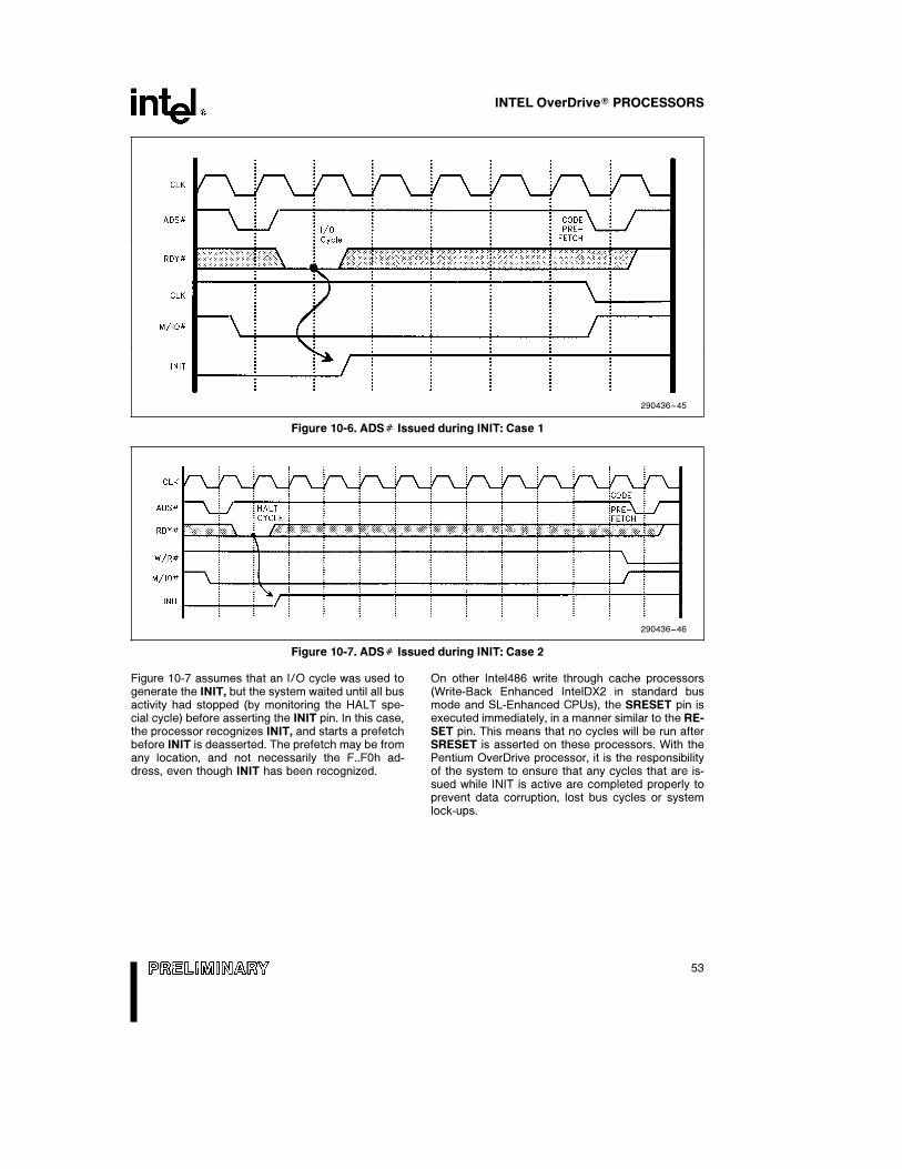
INTEL OverDriveÉ PROCESSORS
290436–45
Figure 10-6. ADSÝ Issued during INIT: Case 1
290436–46
Figure 10-7. ADSÝ Issued during INIT: Case 2
Figure 10-7 assumes that an I/O cycle was used togenerate the INIT, but the system waited until all busactivity had stopped (by monitoring the HALT spe-cial cycle) before asserting the INIT pin. In this case,the processor recognizes INIT, and starts a prefetchbefore INIT is deasserted. The prefetch may be fromany location, and not necessarily the F..F0h ad-dress, even though INIT has been recognized.
On other Intel486 write through cache processors(Write-Back Enhanced IntelDX2 in standard busmode and SL-Enhanced CPUs), the SRESET pin isexecuted immediately, in a manner similar to the RE-SET pin. This means that no cycles will be run afterSRESET is asserted on these processors. With thePentium OverDrive processor, it is the responsibilityof the system to ensure that any cycles that are is-sued while INIT is active are completed properly toprevent data corruption, lost bus cycles or systemlock-ups.
53
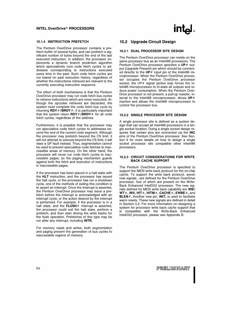
INTEL OverDriveÉ PROCESSORS
10.1.4 INSTRUCTION PREFETCH
The Pentium OverDrive processor contains a pre-fetch buffer of several bytes, and can prefetch a sig-nificant number of bytes beyond the end of the lastexecuted instruction. In addition, the processor im-plements a dynamic branch prediction algorithmwhich speculatively runs code fetch cycles to ad-dresses corresponding to instructions executedsome time in the past. Such code fetch cycles arerun based on past execution history, regardless ofwhether the instructions retrieved are relevant to thecurrently executing instruction sequence.
The effect of both mechanisms is that the PentiumOverDrive processor may run code fetch bus cyclesto retrieve instructions which are never executed. Al-though the opcodes retrieved are discarded, thesystem must complete the code fetch bus cycle byreturning RDYÝ/BRDYÝ. It is particularly importantthat the system return RDYÝ/BRDYÝ for all codefetch cycles, regardless of the address.
Furthermore, it is possible that the processor mayrun speculative code fetch cycles to addresses be-yond the end of the current code segment. Althoughthe processor may prefetch beyond the CS limit, itwill not attempt to execute beyond the CS limit, it willraise a GP fault instead. Thus, segmentation cannotbe used to prevent speculative code fetches to inac-cessible areas of memory. On the other hand, theprocessor will never run code fetch cycles to inac-cessible pages, so the paging mechanism guardsagainst both the fetch and execution of instructionsin inaccessible pages.
If the processor has been placed in a halt state withthe HLT instruction, and the processor has issuedthe halt cycle, or the processor has run a shutdowncycle, one of the methods of exiting this condition isto assert an interrupt. Once the interrupt is asserted,the Pentium OverDrive processor may issue a pre-fetch before the interrupt is acknowledged with aninterrupt cycle, or the action desired by the interruptis performed. For example, if the processor is in ahalt state, and the FLUSHÝ interrupt is asserted,the processor could exit the halt state, perform aprefetch, and then start driving the write backs forthe flush operation. Prefetches of this type may berun after any interrupt, including INTR.
For memory reads and writes, both segmentationand paging prevent the generation of bus cycles toinaccessible regions of memory.
10.2 Upgrade Circuit Design
10.2.1 DUAL PROCESSOR SITE DESIGN
The Pentium OverDrive processor can reside on thesame processor bus as an Intel486 processors. ThePentium OverDrive processor specifies a UPÝ out-put (Upgrade Present) pin which should be connect-ed directly to the UPÝ input pin of the Intel486 mi-croprocessor. When the Pentium OverDrive proces-sor occupies the Pentium OverDrive processorsocket, the UPÝ signal (active low) forces the In-tel486 microprocessor to tri-state all outputs and re-duce power consumption. When the Pentium Over-Drive processor is not present, a pull-up resistor, in-ternal to the Intel486 microprocessor, drives UPÝinactive and allows the Intel486 microprocessor tocontrol the processor bus.
10.2.2 SINGLE PROCESSOR SITE DESIGN
A single processor site is defined as a system de-sign that can accept all Intel486 processors in a sin-gle socket location. Doing a single socket design re-quires that certain pins are connected via the INCpins of the Pentium OverDrive processor. See Sec-tion 9 for more details on how to design a singlesocket processor site compatible other Intel486processors.
10.2.3 CIRCUIT CONSIDERATIONS FOR WRITEBACK CACHE SUPPORT
The Pentium OverDrive processor is specified tosupport the MESI write back protocol for the on-chipcache. To support the write back protocol, sevennew signals , are defined for the Pentium OverDriveprocessor, four of which are present on the Write-Back Enhanced IntelDX2 processor. The new sig-nals defined for MESI write back capability are WB/WTÝ, INV, HITÝ, HITMÝ, CACHEÝ, EWBEÝ, andBLENÝ. Another new pin, INIT, is used to facilitatewarm resets. These new signals are defined in detailin Section 5.2. For more information on designing asystem for processor write back cache support thatis compatible with the Write-Back EnhancedIntelDX2 processor, please see Appendix B.
54
INTEL OverDriveÉ PROCESSORS
10.3 Software Considerations
10.3.1 EXTERNAL BUS CYCLE ORDERING
10.3.1.1 Write Buffers and Memory Ordering
The Pentium OverDrive processor has write buffersto enhance the performance of consecutive writesto memory. Writes in these buffers are driven out onthe external bus in the order they were generated bythe processor core. No reads (as a result of cachemiss) are reordered around previously generatedwrites sitting in the write buffers (Unlike the IntelDX2processor). The implication of this is that the writebuffers will be emptied before a subsequent proces-sor generated bus cycle is run on the external bus.
It should be noted that only memory writes are buff-ered and I/O writes are not. There is no guaranteeof synchronization between completion of memorywrites on the bus and instruction execution after thewrite. The OUT instruction or a serializing instructionneeds to be executed to synchronize writes with thenext instruction. Please refer to the Pentium Proces-sor Programmers Reference Manual for informationon serializing instructions.
No re-ordering of read cycles occurs on the PentiumOverDrive processor. Specifically, the write buffersare emptied before the IN instruction is executed.
10.3.1.2 External Event Synchronization
When the value of NMI, INTR, FLUSHÝ, SMIÝ orINIT changes as the result of executing an OUT in-struction, these inputs must be at a valid state threeclocks before RDYÝ/BRDYÝ is returned to ensurethat the new value will be recognized before the nextinstruction is executed.
Note that if an OUT instruction is used to modifyA20MÝ, this will not affect previously prefetched in-structions. A serializing instruction must be executedto guarantee recognition of A20MÝ before a specif-ic instruction.
10.3.2 MODEL SPECIFIC REGISTERS
The Pentium OverDrive processor defines certainModel Specific Registers that are used in executiontracing, performance monitoring and testing. They
are unique to the Pentium OverDrive processor andmay or may not be implemented in the same way infuture processors.
Please contact Intel for more information on themodel specific registers.
10.3.3 EXCEPTION PRIORITIES
Exceptions are serviced and recognized on theboundary between instructions. The instructionpointer pushed onto the stack for the interrupt han-dler points to the next instruction. The priority amongsimultaneous exceptions is as follows (interrupt vec-tor numbers are shown in decimal in parentheses):
Trap on the previous instruction:
# Breakpoint (Ý3)
External Interrupts:
# FLUSHÝ
# SMIÝ
# INIT
# NMI
# INTR
Floating Point Errors:
# FERRÝ
External Interrupt:
# STPCLKÝ
Faults on Fetching Next Instruction:
# Code Seg Limit Violation (Ý13), Page Fault onprefetch (Ý14) (the relative priority unpredict-able)
Faults in Decoding the next Instruction:
# Invalid Opcode (Ý6), Device Not Available(Ý7)
# General Protection Fault for InstructionLength l 15B (Ý13)
Faults on Executing an Instruction (These may occurin a manner that varies from implementation to im-plementation as necessary to insure functional cor-rectness. They are not listed in any particular order):
# General Detect (Ý1)
# FP Error (from previous FP instruction) (Ý16)
# Interrupt on Overflow (Ý4)
# Bound (Ý5)
# Invalid TSS (Ý10)
55
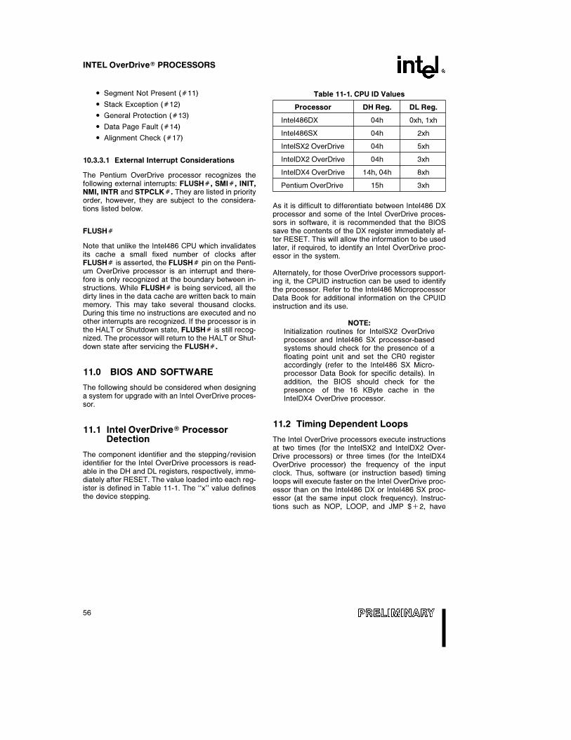
INTEL OverDriveÉ PROCESSORS
# Segment Not Present (Ý11)
# Stack Exception (Ý12)
# General Protection (Ý13)
# Data Page Fault (Ý14)
# Alignment Check (Ý17)
10.3.3.1 External Interrupt Considerations
The Pentium OverDrive processor recognizes thefollowing external interrupts: FLUSHÝ, SMIÝ, INIT,NMI, INTR and STPCLKÝ. They are listed in priorityorder, however, they are subject to the considera-tions listed below.
FLUSHÝ
Note that unlike the Intel486 CPU which invalidatesits cache a small fixed number of clocks afterFLUSHÝ is asserted, the FLUSHÝ pin on the Penti-um OverDrive processor is an interrupt and there-fore is only recognized at the boundary between in-structions. While FLUSHÝ is being serviced, all thedirty lines in the data cache are written back to mainmemory. This may take several thousand clocks.During this time no instructions are executed and noother interrupts are recognized. If the processor is inthe HALT or Shutdown state, FLUSHÝ is still recog-nized. The processor will return to the HALT or Shut-down state after servicing the FLUSHÝ.
11.0 BIOS AND SOFTWARE
The following should be considered when designinga system for upgrade with an Intel OverDrive proces-sor.
11.1 Intel OverDriveÉ ProcessorDetection
The component identifier and the stepping/revisionidentifier for the Intel OverDrive processors is read-able in the DH and DL registers, respectively, imme-diately after RESET. The value loaded into each reg-ister is defined in Table 11-1. The ‘‘x’’ value definesthe device stepping.
Table 11-1. CPU ID Values
Processor DH Reg. DL Reg.
Intel486DX 04h 0xh, 1xh
Intel486SX 04h 2xh
IntelSX2 OverDrive 04h 5xh
IntelDX2 OverDrive 04h 3xh
IntelDX4 OverDrive 14h, 04h 8xh
Pentium OverDrive 15h 3xh
As it is difficult to differentiate between Intel486 DXprocessor and some of the Intel OverDrive proces-sors in software, it is recommended that the BIOSsave the contents of the DX register immediately af-ter RESET. This will allow the information to be usedlater, if required, to identify an Intel OverDrive proc-essor in the system.
Alternately, for those OverDrive processors support-ing it, the CPUID instruction can be used to identifythe processor. Refer to the Intel486 MicroprocessorData Book for additional information on the CPUIDinstruction and its use.
NOTE:Initialization routines for IntelSX2 OverDriveprocessor and Intel486 SX processor-basedsystems should check for the presence of afloating point unit and set the CR0 registeraccordingly (refer to the Intel486 SX Micro-processor Data Book for specific details). Inaddition, the BIOS should check for thepresence of the 16 KByte cache in theIntelDX4 OverDrive processor.
11.2 Timing Dependent Loops
The Intel OverDrive processors execute instructionsat two times (for the IntelSX2 and IntelDX2 Over-Drive processors) or three times (for the IntelDX4OverDrive processor) the frequency of the inputclock. Thus, software (or instruction based) timingloops will execute faster on the Intel OverDrive proc-essor than on the Intel486 DX or Intel486 SX proc-essor (at the same input clock frequency). Instruc-tions such as NOP, LOOP, and JMP $a2, have
56

INTEL OverDriveÉ PROCESSORS
been used by BIOS to implement timing loops thatare required, for example, to enforce recovery timebetween consecutive accesses for I/O devices.These instruction based timing loop implementa-tions may require modification for systems intendedto be upgradable with the Intel OverDrive proces-sors.
In order to avoid any incompatibilities, it is recom-mended that timing requirements be implemented inhardware rather than in software. This providestransparency and also does not require any changein BIOS or I/O device drivers in the future whenmoving to higher processor clock speeds. As an ex-ample, a timing routine may be implemented as fol-lows: The software performs a dummy I/O instruc-tion to an unused I/O port. The hardware for the buscontroller logic recognizes this I/O instruction anddelays the termination of the I/O cycle to the proc-essor by keeping RDYÝ or BRDYÝ deasserted forthe appropriate amount of time.
11.3 Test Register Access on thePentiumÉ OverDriveÉ Processor
The IntelDX2 processor has test registers which al-low OEM’s to test the functionality of different areasof the component. These test registers are ac-cessed on the Intel486 processor family using the‘‘MOV reg, TRx and MOV TRx, reg’’ instructions.These instructions are not available on the PentiumOverDrive processor. Any attempt to execute themwill cause a invalid opcode exception. The PentiumOverDrive processor uses the Model Specific Regis-ters (MSR’s) to implement on chip testing. TheseMSR’s are accessed using the RDMSR andWRMSR instructions. BIOS must recognize this fun-damental difference between the Pentium OverDriveprocessor and the IntelDX2 processor and act ac-cordingly.
12.0 PentiumÉ OverDriveÉPROCESSOR TESTABILITY
12.1 Introduction
This section describes the features which are includ-ed in the Pentium OverDrive processor for the pur-pose of enhancing the testability of the part. Thecapabilities of the Intel486 processor test hooks areincluded in the processor, however they are imple-mented differently. In addition, new test featureswere added to assure timely testing and productionof a system product. All features described here arealso present in the Pentium processor.
Internal component testing through the Built In SelfTest (BIST) feature of the Pentium OverDrive proc-essor provides 100% single stuck at fault coverageof the microcode ROM and large PLAs. Some test-ing of the instruction cache, data cache, TranslationLookaside Buffers (TLBs), and Branch Target Buffer(BTB) is also performed. In addition, the constantROMs are checked.
The production version of the Pentium OverDriveprocessor will not include the boundary scan or test-ability pins.
Several test registers are also included in the Penti-um OverDrive processor to simplify access to all on-chip caches and TLBs. These test registers on theprocessor are not compatible with the definitions forthe test registers on the IntelDX2 processor, and willbe provided by Intel at a later date. For the latestinformation on these test registers, please contactIntel.
The following list summarizes the Pentium Over-Drive processor testability features:
# Built In Self Test
# Cache and TLB Test Registers
# Tristate Test Mode
Table 12-1. PentiumÉ OverDriveÉ Processor RESET Modes
RESET INITType of Effect on Effect on Effect on SMMReset I/D Caches FP Registers Base Register
0 0 None Not Applicable Not Applicable Not Applicable
0 1 Warm Reset None None None
1 X Cold Reset Invalidated Initialized Invalidated(w/ BIST)
1 X Cold Reset Invalidated Undefined Invalidated(w/o BIST)
57
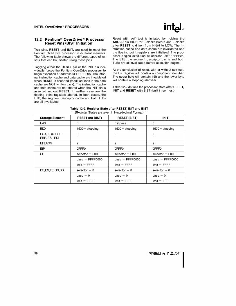
INTEL OverDriveÉ PROCESSORS
12.2 PentiumÉ OverDriveÉ ProcessorReset Pins/BIST Initiation
Two pins, RESET and INIT, are used to reset thePentium OverDrive processor in different manners.The following table shows the different types of re-sets that can be initiated using these pins.
Toggling either the RESET pin or the INIT pin indi-vidually forces the Pentium OverDrive processor tobegin execution at address 0FFFFFFF0h. The inter-nal instruction cache and data cache are invalidatedwhen RESET is asserted (modified lines in the datacache are NOT written back). The instruction cacheand data cache are not altered when the INIT pin isasserted without RESET. In neither case are thefloating point registers altered. In both cases, theBTB, the segment descriptor cache and both TLBsare all invalidated.
Reset with self test is initiated by holding theAHOLD pin HIGH for 2 clocks before and 2 clocksafter RESET is driven from HIGH to LOW. The in-struction cache and data cache are invalidated andthe floating point registers are initialized. The proc-essor begins execution at address 0xFFFFFFF0h.The BTB, the segment descriptor cache and bothTLBs are all invalidated before execution begins.
At the conclusion of reset, with or without self test,the DX register will contain a component identifier.The upper byte will contain 15h and the lower bytewill contain a stepping identifier.
Table 12-2 defines the processor state after RESET,INIT and RESET with BIST (built in self test).
Table 12-2. Register State after RESET, INIT and BIST
(Register States are given in Hexadecimal Format)
Storage Element RESET (no BIST) RESET (BIST) INIT
EAX 0 0 if pass 0
EDX 1530astepping 1530astepping 1530astepping
ECX, EBX, ESP 0 0 0
EBP, ESI, EDI
EFLAGS 2 2 2
EIP 0FFF0 0FFF0 0FFF0
CS selector e F000 selector e F000 selector e F000
base e FFFF0000 base e FFFF0000 base e FFFF0000
limit e FFFF limit e FFFF limit e FFFF
DS,ES,FE,GS,SS selector e 0 selector e 0 selector e 0
base e 0 base e 0 base e 0
limit e FFFF limit e FFFF limit e FFFF
58
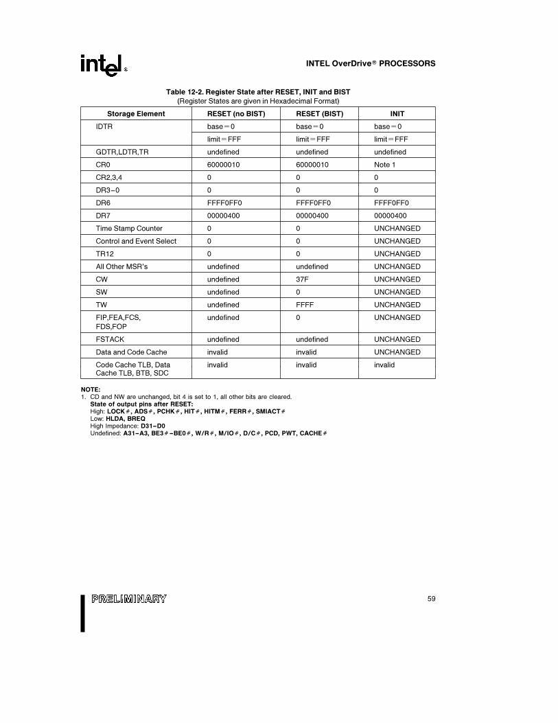
INTEL OverDriveÉ PROCESSORS
Table 12-2. Register State after RESET, INIT and BIST
(Register States are given in Hexadecimal Format)
Storage Element RESET (no BIST) RESET (BIST) INIT
IDTR basee0 basee0 basee0
limiteFFF limiteFFF limiteFFF
GDTR,LDTR,TR undefined undefined undefined
CR0 60000010 60000010 Note 1
CR2,3,4 0 0 0
DR3–0 0 0 0
DR6 FFFF0FF0 FFFF0FF0 FFFF0FF0
DR7 00000400 00000400 00000400
Time Stamp Counter 0 0 UNCHANGED
Control and Event Select 0 0 UNCHANGED
TR12 0 0 UNCHANGED
All Other MSR’s undefined undefined UNCHANGED
CW undefined 37F UNCHANGED
SW undefined 0 UNCHANGED
TW undefined FFFF UNCHANGED
FIP,FEA,FCS, undefined 0 UNCHANGED
FDS,FOP
FSTACK undefined undefined UNCHANGED
Data and Code Cache invalid invalid UNCHANGED
Code Cache TLB, Data invalid invalid invalidCache TLB, BTB, SDC
NOTE:1. CD and NW are unchanged, bit 4 is set to 1, all other bits are cleared.
State of output pins after RESET:High: LOCKÝ, ADSÝ, PCHKÝ, HITÝ, HITMÝ, FERRÝ, SMIACTÝLow: HLDA, BREQHigh Impedance: D31–D0Undefined: A31–A3, BE3Ý–BE0Ý, W/RÝ, M/IOÝ, D/CÝ, PCD, PWT, CACHEÝ
59
INTEL OverDriveÉ PROCESSORS
12.3 Built In Self Test (BIST)
Self test is initiated by holding the AHOLD pin HIGHfor the clock before RESET changes from HIGH toLOW. If asserted asynchronously, AHOLD must beasserted two clocks before and two clocks afterRESET to guarantee recognition.
No bus cycles are run by the Pentium OverDriveprocessor during self test. The duration of self test isapproximately 219 internal clocks. Approximately70% of the devices in the processor are tested byBIST.
The Pentium OverDrive processor BIST consists oftwo parts: hardware self test and microcode selftest.
During the hardware portion of BIST, the microcodeand all large PLAs are tested. All possible input com-binations of the microcode ROM and PLAs are test-ed.
The constant ROMs, BTB, TLBs, and all caches aretested by the microcode portion of BIST. The arraytests (caches, TLBs, and BTB) have two passes. Onthe first pass, data patterns are written to arrays,read back and checked for mismatches. The secondpass writes the complement of the initial data pat-tern, reads it back, and checks for mismatches. Theconstant ROMs are tested by using the microcodeto add various constants and check the resultagainst a stored value.
Upon completion of BIST, the cumulative result of alltests are stored in the EAX register. If EAX contains0x0h, then all checks passed; any non-zero resultindicates a faulty unit.
During BIST, EADSÝ should not be used to performsnoops, otherwise false HITMÝ indications, with nocorresponding write back cycles, can occur.
12.4 Tri-State Test Mode
The Pentium OverDrive processor provides the abili-ty to float all its outputs and bi-directional pins. Thisincludes pins that are floated during bus hold as well
as some pins that are not normally floated duringnormal operation. When the Pentium OverDriveprocessor is in tri-state test mode, external testingcan be used to test on board connections.
The tri-state test mode is invoked by drivingFLUSHÝ low for 2 clocks before and 2 clocks afterRESET going low. The outputs are guaranteed to tri-state no later than 10 clocks after RESET goes low.The processor will remain in tri-state test mode untilthe next RESET.
12.5 Cache, TLB and BTB TestRegisters
The Pentium OverDrive processor contains severaltest registers. The purpose of the test registers is toprovide direct access to the processor caches,TLBs, and BTB, so user programs can easily exer-cise these structures. Because the architecture ofthe caches, TLBs, and BTB is different, a differentset of test registers (along with a different test mech-anism) is required for each. Most test registers canbe shared between the code and data caches.
Since much of the testability hardware is used forother purposes during normal operation of the Penti-um OverDrive processor, some restrictions may ex-ist on what software may do while testability opera-tions are being run.
Please contact Intel for more information on thePentium OverDrive processor Cache, TLB, and BTBTest Registers.
12.6 Fan Protection Mechanism andTHermal ERRor Bit
The Pentium OverDrive processor employs an activefan/heatsink unit to assist in cooling the processor.Another integral part of this cooling solution is theability for software to poll the status of the fan todetermine if the fan has fallen to a speed that isunacceptable to cool the processor. Should the fanfall into a speed range that is too slow, a controlregister will record the event. (For more information,please contact Intel.)
60
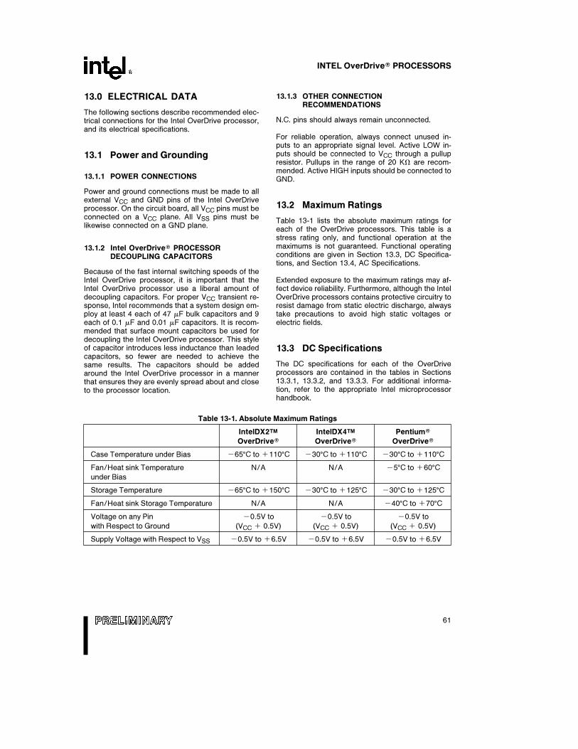
INTEL OverDriveÉ PROCESSORS
13.0 ELECTRICAL DATA
The following sections describe recommended elec-trical connections for the Intel OverDrive processor,and its electrical specifications.
13.1 Power and Grounding
13.1.1 POWER CONNECTIONS
Power and ground connections must be made to allexternal VCC and GND pins of the Intel OverDriveprocessor. On the circuit board, all VCC pins must beconnected on a VCC plane. All VSS pins must belikewise connected on a GND plane.
13.1.2 Intel OverDriveÉ PROCESSORDECOUPLING CAPACITORS
Because of the fast internal switching speeds of theIntel OverDrive processor, it is important that theIntel OverDrive processor use a liberal amount ofdecoupling capacitors. For proper VCC transient re-sponse, Intel recommends that a system design em-ploy at least 4 each of 47 mF bulk capacitors and 9each of 0.1 mF and 0.01 mF capacitors. It is recom-mended that surface mount capacitors be used fordecoupling the Intel OverDrive processor. This styleof capacitor introduces less inductance than leadedcapacitors, so fewer are needed to achieve thesame results. The capacitors should be addedaround the Intel OverDrive processor in a mannerthat ensures they are evenly spread about and closeto the processor location.
13.1.3 OTHER CONNECTIONRECOMMENDATIONS
N.C. pins should always remain unconnected.
For reliable operation, always connect unused in-puts to an appropriate signal level. Active LOW in-puts should be connected to VCC through a pullupresistor. Pullups in the range of 20 KX are recom-mended. Active HIGH inputs should be connected toGND.
13.2 Maximum Ratings
Table 13-1 lists the absolute maximum ratings foreach of the OverDrive processors. This table is astress rating only, and functional operation at themaximums is not guaranteed. Functional operatingconditions are given in Section 13.3, DC Specifica-tions, and Section 13.4, AC Specifications.
Extended exposure to the maximum ratings may af-fect device reliability. Furthermore, although the IntelOverDrive processors contains protective circuitry toresist damage from static electric discharge, alwaystake precautions to avoid high static voltages orelectric fields.
13.3 DC Specifications
The DC specifications for each of the OverDriveprocessors are contained in the tables in Sections13.3.1, 13.3.2, and 13.3.3. For additional informa-tion, refer to the appropriate Intel microprocessorhandbook.
Table 13-1. Absolute Maximum Ratings
IntelDX2TM IntelDX4TM PentiumÉOverDriveÉ OverDriveÉ OverDriveÉ
Case Temperature under Bias b65§C to a110§C b30§C to a110§C b30§C to a110§CFan/Heat sink Temperature N/A N/A b5§C to a60§Cunder Bias
Storage Temperature b65§C to a150§C b30§C to a125§C b30§C to a125§CFan/Heat sink Storage Temperature N/A N/A b40§C to a70§CVoltage on any Pin b0.5V to b0.5V to b0.5V to
with Respect to Ground (VCC a 0.5V) (VCC a 0.5V) (VCC a 0.5V)
Supply Voltage with Respect to VSS b0.5V to a6.5V b0.5V to a6.5V b0.5V to a6.5V
61
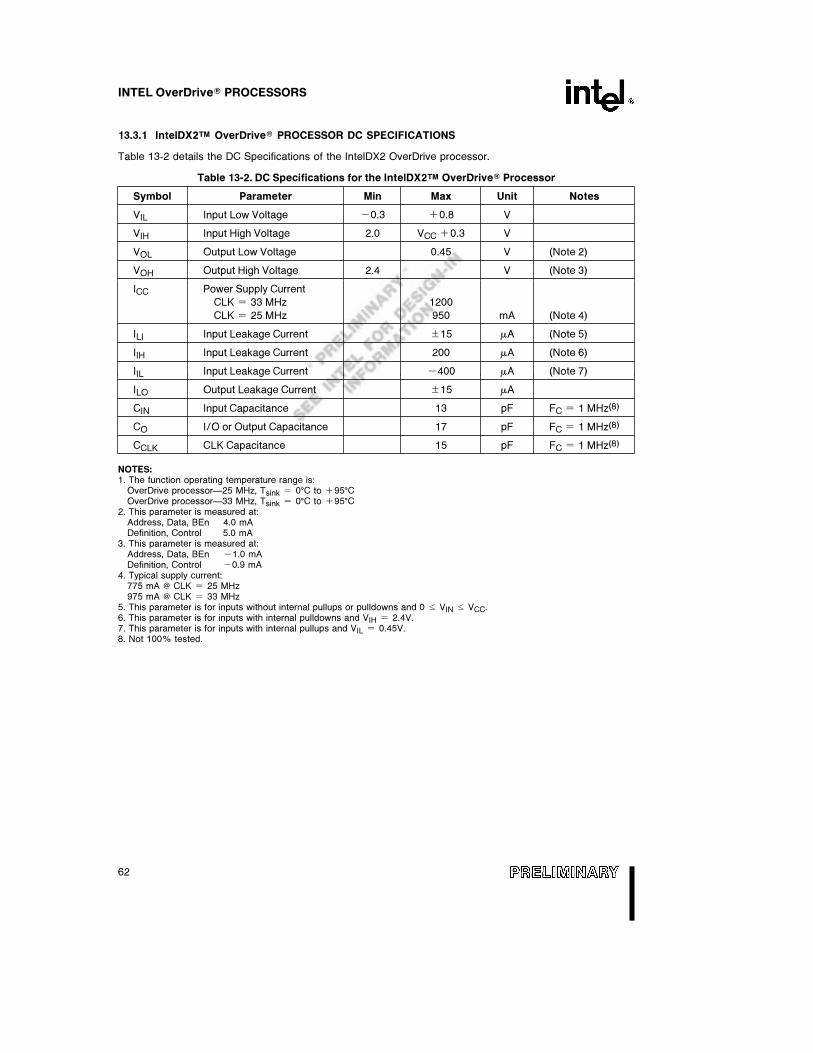
INTEL OverDriveÉ PROCESSORS
13.3.1 IntelDX2TM OverDriveÉ PROCESSOR DC SPECIFICATIONS
Table 13-2 details the DC Specifications of the IntelDX2 OverDrive processor.
Table 13-2. DC Specifications for the IntelDX2TM OverDriveÉ Processor
Symbol Parameter Min Max Unit Notes
VIL Input Low Voltage b0.3 a0.8 V
VIH Input High Voltage 2.0 VCC a0.3 V
VOL Output Low Voltage 0.45 V (Note 2)
VOH Output High Voltage 2.4 V (Note 3)
ICC Power Supply Current
CLK e 33 MHz 1200
CLK e 25 MHz 950 mA (Note 4)
ILI Input Leakage Current g15 mA (Note 5)
IIH Input Leakage Current 200 mA (Note 6)
IIL Input Leakage Current b400 mA (Note 7)
ILO Output Leakage Current g15 mA
CIN Input Capacitance 13 pF FC e 1 MHz(8)
CO I/O or Output Capacitance 17 pF FC e 1 MHz(8)
CCLK CLK Capacitance 15 pF FC e 1 MHz(8)
NOTES:1. The function operating temperature range is:
OverDrive processorÐ25 MHz, Tsink e 0§C to a95§COverDrive processorÐ33 MHz, Tsink e 0§C to a95§C
2. This parameter is measured at:Address, Data, BEn 4.0 mADefinition, Control 5.0 mA
3. This parameter is measured at:Address, Data, BEn b1.0 mADefinition, Control b0.9 mA
4. Typical supply current:775 mA @ CLK e 25 MHz975 mA @ CLK e 33 MHz
5. This parameter is for inputs without internal pullups or pulldowns and 0 s VIN s VCC.6. This parameter is for inputs with internal pulldowns and VIH e 2.4V.7. This parameter is for inputs with internal pullups and VIL e 0.45V.8. Not 100% tested.
62
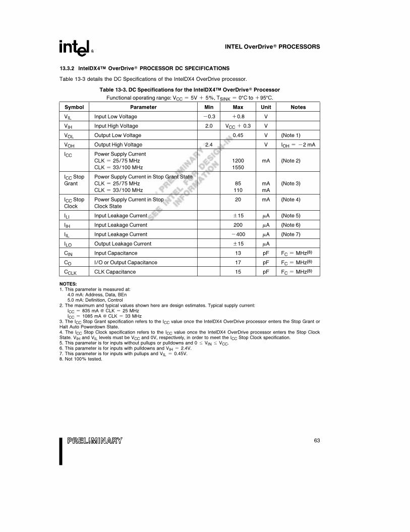
INTEL OverDriveÉ PROCESSORS
13.3.2 IntelDX4TM OverDriveÉ PROCESSOR DC SPECIFICATIONS
Table 13-3 details the DC Specifications of the IntelDX4 OverDrive processor.
Table 13-3. DC Specifications for the IntelDX4TM OverDriveÉ Processor
Functional operating range: VCC e 5V a 5%, TSINK e 0§C to a95§C.
Symbol Parameter Min Max Unit Notes
VIL Input Low Voltage b0.3 a0.8 V
VIH Input High Voltage 2.0 VCC a 0.3 V
VOL Output Low Voltage 0.45 V (Note 1)
VOH Output High Voltage 2.4 V IOH e b2 mA
ICC Power Supply Current
CLK e 25/75 MHz 1200 mA (Note 2)
CLK e 33/100 MHz 1550
ICC Stop Power Supply Current in Stop Grant State
Grant CLK e 25/75 MHz 85 mA (Note 3)
CLK e 33/100 MHz 110 mA
ICC Stop Power Supply Current in Stop 20 mA (Note 4)
Clock Clock State
ILI Input Leakage Current g15 mA (Note 5)
IIH Input Leakage Current 200 mA (Note 6)
IIL Input Leakage Current b400 mA (Note 7)
ILO Output Leakage Current g15 mA
CIN Input Capacitance 13 pF FC e MHz(8)
CO I/O or Output Capacitance 17 pF FC e MHz(8)
CCLK CLK Capacitance 15 pF FC e MHz(8)
NOTES:1. This parameter is measured at:
4.0 mA: Address, Data, BEn5.0 mA: Definition, Control
2. The maximum and typical values shown here are design estimates. Typical supply current:ICC e 835 mA @ CLK e 25 MHzICC e 1085 mA @ CLK e 33 MHz
3. The ICC Stop Grant specification refers to the ICC value once the IntelDX4 OverDrive processor enters the Stop Grant orHalt Auto Powerdown State.4. The ICC Stop Clock specification refers to the ICC value once the IntelDX4 OverDrive processor enters the Stop ClockState. VIH and VIL levels must be VCC and 0V, respectively, in order to meet the ICC Stop Clock specification.5. This parameter is for inputs without pullups or pulldowns and 0 s VIN s VCC.6. This parameter is for inputs with pulldowns and VIH e 2.4V.7. This parameter is for inputs with pullups and VIL e 0.45V.8. Not 100% tested.
63
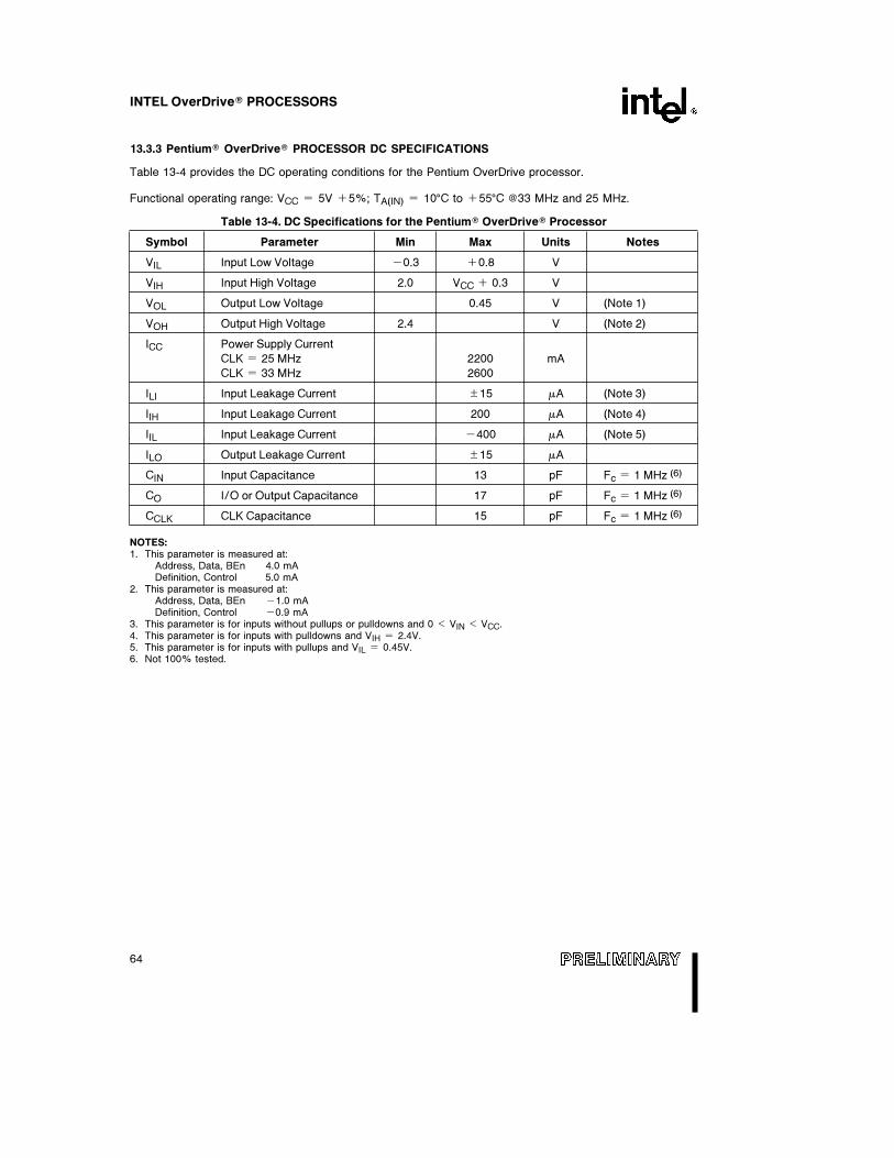
INTEL OverDriveÉ PROCESSORS
13.3.3 PentiumÉ OverDriveÉ PROCESSOR DC SPECIFICATIONS
Table 13-4 provides the DC operating conditions for the Pentium OverDrive processor.
Functional operating range: VCC e 5V a5%; TA(IN) e 10§C to a55§C @33 MHz and 25 MHz.
Table 13-4. DC Specifications for the PentiumÉ OverDriveÉ Processor
Symbol Parameter Min Max Units Notes
VIL Input Low Voltage b0.3 a0.8 V
VIH Input High Voltage 2.0 VCC a 0.3 V
VOL Output Low Voltage 0.45 V (Note 1)
VOH Output High Voltage 2.4 V (Note 2)
ICC Power Supply Current
CLK e 25 MHz 2200 mA
CLK e 33 MHz 2600
ILI Input Leakage Current g15 mA (Note 3)
IIH Input Leakage Current 200 mA (Note 4)
IIL Input Leakage Current b400 mA (Note 5)
ILO Output Leakage Current g15 mA
CIN Input Capacitance 13 pF Fc e 1 MHz (6)
CO I/O or Output Capacitance 17 pF Fc e 1 MHz (6)
CCLK CLK Capacitance 15 pF Fc e 1 MHz (6)
NOTES:1. This parameter is measured at:
Address, Data, BEn 4.0 mADefinition, Control 5.0 mA
2. This parameter is measured at:Address, Data, BEn b1.0 mADefinition, Control b0.9 mA
3. This parameter is for inputs without pullups or pulldowns and 0 k VIN k VCC.4. This parameter is for inputs with pulldowns and VIH e 2.4V.5. This parameter is for inputs with pullups and VIL e 0.45V.6. Not 100% tested.
64
INTEL OverDriveÉ PROCESSORS
13.4 AC Specifications
The AC specifications for each of the OverDriveprocessors are contained in the tables in Sections13.4.1, 13.4.2 and 13.4.3. These specifications con-sist of output delays, input setup requirements andinput hold requirements. All AC specifications arerelative to the rising edge of the CLK signal.
AC specification measurements are defined by Fig-ures 13-1 through 13-6. All timings are referenced to1.5V, unless otherwise specified. Inputs must bedriven to the voltage levels indicated by Figure 13-3when AC specifications are measured. Intel Over-Drive processor output delays are specified withminimum and maximum limits, measured as shown.The minimum Intel OverDrive processor delay timesare hold times provided to external circuitry. IntelOverDrive processor input setup and hold times arespecified as minimums, defining the smallest ac-ceptable sampling window. Within the sampling win-dow, a synchronous signal must be stable for cor-rect Intel OverDrive processor operation.
Table 13-5 defines the AC timing specifications for a33 MHz system. Table 13-7 defines the AC timingspecifications for a 25 MHz system. Table 13-8 de-fines the AC timing specifications for a 20 MHz sys-tem. Table 13-8 defines the AC timing specificationsfor a 16 MHz system.
Each Intel OverDrive processor meets the AC speci-fications for the processor it is upgrading. For exam-ple, a 100 MHz IntelDX4 OverDrive processor
meets the system AC timing specifications for the33 MHz processor it is upgrading.
Refer to Sections 13.4.1 through 13.4.3 for any tim-ing differences from those specified in the followingtables.
For additional information, refer to the appropriateIntel microprocessor handbook.
13.4.1 IntelDX2TM OverDriveÉ PROCESSOR ACSPECIFICATIONS
The IntelDX2 OverDrive processor can be placedinto an existing 16 MHz, 20 MHz, 25 MHz or 33 MHzIntel486 system, doubling the internal processorspeed to 32 MHz, 40 MHz, 50 MHz or 66 MHz, re-spectively.
Tables 13-5 through 13-8 contain the AC timingspecifications for the processors in those systems.
13.4.2 IntelDX4TM OverDriveÉ PROCESSOR ACSPECIFICATIONS
The IntelDX4 OverDrive processor can be placedinto an existing 16 MHz, 20 MHz, 25 MHz or 33 MHzIntel486 system, tripling the internal processorspeed to 48 MHz, 60 MHz, 75 MHz or 100 MHz,respectively.
Tables 13-5 through 13-8 contain the AC timingspecifications for the processors in those systems.
65

INTEL OverDriveÉ PROCESSORS
Table 13-5. 33 MHz Intel Processor Characteristics(1)
VCC e 5V g5%; Tsink e See Note 6; CI e 50 pF unless otherwise specified(3)
Symbol Parameter Min Max Unit Figure Notes
Frequency 8 33 MHz 1X Clock Driven toOverDrive processor
t1 CLK Period 30 125 ns 13-1
t1a CLK Period Stability 0.1% D Adjacent Clocks
t2 CLK High Time 11 ns 13-1 at 2V
t3 CLK Low Time 11 ns 13-1 at 0.8V
t4 CLK Fall Time 3 ns 13-1 2V to 0.8V
t5 CLK Rise Time 3 ns 13-1 0.8V to 2V
t6 A2–A31, PWT, PCD, BE0–3Ý, M/IOÝ, 3 14 ns 13-5 (Note 4)D/CÝ, W/RÝ, ADSÝ, LOCKÝ, SMIACTÝ,FERRÝ, BREQ, HLDA Valid Delay
t7 A2–A31, PWT, PCD, BE0–3Ý, M/IOÝ, 20 ns 13-6 (Note 2)D/CÝ, W/RÝ, ADSÝ, LOCKÝ Float Delay
t8 PCHKÝ Valid Delay 3 22 ns 13-4 (Note 4)
t8a BLASTÝ, PLOCKÝ Valid Delay 3 20 ns 13-5 (Note 4)
t9 BLASTÝ, PLOCKÝ Float Delay 20 ns 13-6 (Note 2)
t10 D0–D31, DP0–3 Write Data Valid Delay 3 18 ns 13-5 (Note 4)
t11 D0–D31, DP0–3 Write Data Float Delay 20 ns 13-6 (Note 2)
t12 EADSÝ Setup Time 5 ns 13-2
t13 EADSÝ Hold Time 3 ns 13-2
t14 KENÝ, BS16Ý, BS8Ý Setup Time 5 ns 13-2
t15 KENÝ, BS16Ý, BS8Ý Hold Time 3 ns 13-2
t16 RDYÝ, BRDYÝ Setup Time 5 ns 13-3
t17 RDYÝ, BRDYÝ Hold Time 3 ns 13-3
t18 HOLD, AHOLD Setup Time 6 ns 13-2
t18a BOFFÝ Setup Time 7 ns 13-2
t19 HOLD, AHOLD, BOFFÝ Hold Time 3 ns 13-2
t20 RESET, FLUSHÝ, A20MÝ, NMI, INTR, 5 ns 13-2SMIÝ, STPCLKÝ, SRESET, IGNNEÝSetup Time
t21 RESET, FLUSHÝ, A20MÝ, NMI, INTR, 3 ns 13-2SMIÝ, STPCLKÝ, SRESET, IGNNEÝHold Time
t22 D0–D31, DP0–3, A4–A31 Read Setup Time 5 ns 13-2, 13-3
t23 D0–D31, DP0–3, A4–A31 Read Hold Time 3 ns 13-2, 13-3
NOTES:1. To be used for 66 MHz IntelDX2 and 100 MHz IntelDX4 OverDrive processors.2. Not 100% tested. Guaranteed by design characterization.3. All timing specifications assume CL e 50 pF.4. The minimum Intel OverDrive processor output valid delays are hold times provided to external circuitry.5. A reset pulse width of 15 CLK cycles is required for warm resets. Power-up resets require RESET to be asserted for atleast 1 ms after VCC and CLK are stable.6. TSINK temperatures are:
IntelDX2 OverDrive processor: 0§C to a95§CIntelDX4 OverDrive processor: 0§C to a95§C
66
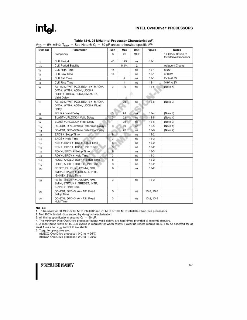
INTEL OverDriveÉ PROCESSORS
Table 13-6. 25 MHz Intel Processor Characteristics(1)
VCC e 5V g5%; Tsink e See Note 6; CI e 50 pF unless otherwise specified(3)
Symbol Parameter Min Max Unit Figure Notes
Frequency 8 25 MHz 1X Clock Driven toOverDrive Processor
t1 CLK Period 40 125 ns 13-1
t1a CLK Period Stability 0.1% D Adjacent Clocks
t2 CLK High Time 14 ns 13-1 at 2V
t3 CLK Low Time 14 ns 13-1 at 0.8V
t4 CLK Fall Time 4 ns 13-1 2V to 0.8V
t5 CLK Rise Time 4 ns 13-1 0.8V to 2V
t6 A2–A31, PWT, PCD, BE0–3Ý, M/IOÝ, 3 19 ns 13-5 (Note 4)
D/CÝ, W/RÝ, ADSÝ, LOCKÝ,
FERRÝ, BREQ, HLDA, SMIACTÝ,
Valid Delay
t7 A2–A31, PWT, PCD, BE0–3Ý, M/IOÝ, 28 ns 13-6 (Note 2)
D/CÝ, W/RÝ, ADSÝ, LOCKÝ Float
Delay
t8 PCHKÝ Valid Delay 3 24 ns 13-4 (Note 4)
t8a BLASTÝ, PLOCKÝ Valid Delay 3 24 ns 13-5 (Note 4)
t9 BLASTÝ, PLOCKÝ Float Delay 28 ns 13-6 (Note 2)
t10 D0–D31, DP0–3 Write Data Valid Delay 3 20 ns 13-5 (Note 4)
t11 D0–D31, DP0–3 Write Data Float Delay 28 ns 13-6 (Note 2)
t12 EADSÝ Setup Time 8 ns 13-2
t13 EADSÝ Hold Time 3 ns 13-2
t14 KENÝ, BS16Ý, BS8Ý Setup Time 8 ns 13-2
t15 KENÝ, BS16Ý, BS8Ý Hold Time 3 ns 13-2
t16 RDYÝ, BRDYÝ Setup Time 8 ns 13-3
t17 RDYÝ, BRDYÝ Hold Time 3 ns 13-3
t18 HOLD, AHOLD, BOFFÝ Setup Time 8 ns 13-2
t19 HOLD, AHOLD, BOFFÝ Hold Time 3 ns 13-2
t20 RESET, FLUSHÝ, A20MÝ, NMI, 8 ns 13-2
SMIÝ, STPCLKÝ, SRESET, INTR,
IGNNEÝ Setup Time
t21 RESET, FLUSHÝ, A20MÝ, NMI, 3 ns 13-2
SMIÝ, STPCLKÝ, SRESET, INTR,
IGNNEÝ Hold Time
t22 D0–D31, DP0–3, A4–A31 Read 5 ns 13-2, 13-3Setup Time
t23 D0–D31, DP0–3, A4–A31 Read 3 ns 13-2, 13-3Hold Time
NOTES:1. To be used for 50 MHz or 60 MHz IntelDX2 and 75 MHz or 100 MHz IntelDX4 OverDrive processors.2. Not 100% tested. Guaranteed by design characterization.3. All timing specifications assume CL e 50 pF.4. The minimum Intel OverDrive processor output valid delays are hold times provided to external circuitry.5. A reset pulse width of 15 CLK cycles is required for warm resets. Power-up resets require RESET to be asserted for atleast 1 ms after VCC and CLK are stable.6. TSINK temperatures are:
IntelDX2 OverDrive processor: 0§C to a95§CIntelDX4 OverDrive processor: 0§C to a95§C
67
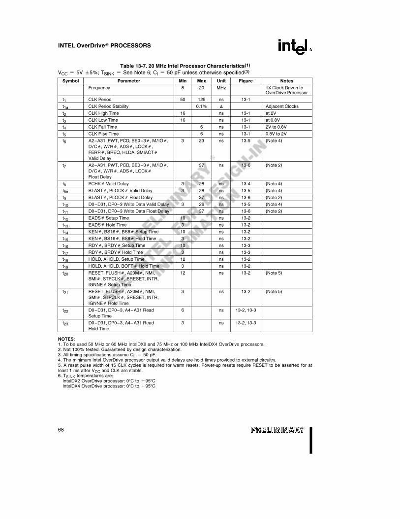
INTEL OverDriveÉ PROCESSORS
Table 13-7. 20 MHz Intel Processor Characteristics(1)
VCC e 5V g5%; TSINK e See Note 6; CI e 50 pF unless otherwise specified(3)
Symbol Parameter Min Max Unit Figure Notes
Frequency 8 20 MHz 1X Clock Driven toOverDrive Processor
t1 CLK Period 50 125 ns 13-1
t1a CLK Period Stability 0.1% D Adjacent Clocks
t2 CLK High Time 16 ns 13-1 at 2V
t3 CLK Low Time 16 ns 13-1 at 0.8V
t4 CLK Fall Time 6 ns 13-1 2V to 0.8V
t5 CLK Rise Time 6 ns 13-1 0.8V to 2V
t6 A2–A31, PWT, PCD, BE0–3Ý, M/IOÝ, 3 23 ns 13-5 (Note 4)
D/CÝ, W/RÝ, ADSÝ, LOCKÝ,
FERRÝ, BREQ, HLDA, SMIACTÝ
Valid Delay
t7 A2–A31, PWT, PCD, BE0–3Ý, M/IOÝ, 37 ns 13-6 (Note 2)
D/CÝ, W/RÝ, ADSÝ, LOCKÝ
Float Delay
t8 PCHKÝ Valid Delay 3 28 ns 13-4 (Note 4)
t8a BLASTÝ, PLOCKÝ Valid Delay 3 28 ns 13-5 (Note 4)
t9 BLASTÝ, PLOCKÝ Float Delay 37 ns 13-6 (Note 2)
t10 D0–D31, DP0–3 Write Data Valid Delay 3 26 ns 13-5 (Note 4)
t11 D0–D31, DP0–3 Write Data Float Delay 37 ns 13-6 (Note 2)
t12 EADSÝ Setup Time 10 ns 13-2
t13 EADSÝ Hold Time 3 ns 13-2
t14 KENÝ, BS16Ý, BS8Ý Setup Time 10 ns 13-2
t15 KENÝ, BS16Ý, BS8Ý Hold Time 3 ns 13-2
t16 RDYÝ, BRDYÝ Setup Time 10 ns 13-3
t17 RDYÝ, BRDYÝ Hold Time 3 ns 13-3
t18 HOLD, AHOLD, Setup Time 12 ns 13-2
t19 HOLD, AHOLD, BOFFÝ Hold Time 3 ns 13-2
t20 RESET, FLUSHÝ, A20MÝ, NMI, 12 ns 13-2 (Note 5)
SMIÝ, STPCLKÝ, SRESET, INTR,
IGNNEÝ Setup Time
t21 RESET, FLUSHÝ, A20MÝ, NMI, 3 ns 13-2 (Note 5)
SMIÝ, STPCLKÝ, SRESET, INTR,
IGNNEÝ Hold Time
t22 D0–D31, DP0–3, A4–A31 Read 6 ns 13-2, 13-3
Setup Time
t23 D0–D31, DP0–3, A4–A31 Read 3 ns 13-2, 13-3
Hold Time
NOTES:1. To be used 50 MHz or 60 MHz IntelDX2 and 75 MHz or 100 MHz IntelDX4 OverDrive processors.2. Not 100% tested. Guaranteed by design characterization.3. All timing specifications assume CL e 50 pF.4. The minimum Intel OverDrive processor output valid delays are hold times provided to external circuitry.5. A reset pulse width of 15 CLK cycles is required for warm resets. Power-up resets require RESET to be asserted for atleast 1 ms after VCC and CLK are stable.6. TSINK temperatures are:
IntelDX2 OverDrive processor: 0§C to a95§CIntelDX4 OverDrive processor: 0§C to a95§C
68

INTEL OverDriveÉ PROCESSORS
Table 13-8. 16 MHz Intel Processor Characteristics(1)
VCC e 5V g5%; TSINK e See Note 6; CI e 50 pF unless otherwise specified
Symbol Parameter Min Max Unit Figure Notes
Frequency 8 16 MHz 1X Clock Driven toOverDrive Processor
t1 CLK Period 62.5 125 ns 13-1
t1a CLK Period Stability 0.1% D Adjacent Clocks
t2 CLK High Time 20 ns 13-1 at 2V
t3 CLK Low Time 20 ns 13-1 at 0.8V
t4 CLK Fall Time 8 ns 13-1 2V to 0.8V
t5 CLK Rise Time 8 ns 13-1 0.8V to 2V
t6 A2–A31, PWT, PCD, BE0–3Ý, M/IOÝ, 3 26 ns 13-5 (Note 4)
D/CÝ, W/RÝ, ADSÝ, LOCKÝ,
FERRÝ, BREQ, HLDA, SMIACTÝ
Valid Delay
t7 A2–A31, PWT, PCD, BE0–3Ý, M/IOÝ, 42 ns 13-6 (Note 2)
D/CÝ, W/RÝ, ADSÝ, LOCKÝ
Float Delay
t8 PCHKÝ Valid Delay 3 35 ns 13-4 (Note 4)
t8a BLASTÝ, PLOCKÝ Valid Delay 3 35 ns 13-5 (Note 4)
t9 BLASTÝ, PLOCKÝ Float Delay 42 ns 13-6 (Note 2)
t10 D0–D31, DP0–3 Write Data Valid Delay 3 30 ns 13-5 (Note 4)
t11 D0–D31, DP0–3 Write Data Float Delay 42 ns 13-6 (Note 2)
t12 EADSÝ Setup Time 12 ns 13-2
t13 EADSÝ Hold Time 4 ns 13-2
t14 KENÝ, BS16Ý, BS8Ý Setup Time 12 ns 13-2
t15 KENÝ, BS16Ý, BS8Ý Hold Time 4 ns 13-2
t16 RDYÝ, BRDYÝ Setup Time 12 ns 13-3
t17 RDYÝ, BRDYÝ Hold Time 4 ns 13-3
t18 HOLD, AHOLD, BOFFÝ Setup Time 12 ns 13-2
t19 HOLD, AHOLD, BOFFÝ Hold Time 4 ns 13-2
t20 RESET, FLUSHÝ, A20MÝ, NMI, 14 ns 13-2 (Note 5)
SMIÝ, STPCLKÝ, SRESET, INTR,
IGNNEÝ Setup Time
t21 RESET, FLUSHÝ, A20MÝ, NMI, 4 ns 13-2 (Note 5)
SMIÝ, STPCLKÝ, SRESET, INTR,
IGNNEÝ Hold Time
t22 D0–D31, DP0–3, A4–A31 Read 10 ns 13-2, 13-3
Setup Time
t23 D0–D31, DP0–3, A4–A31 Read 4 ns 13-2, 13-3
Hold Time
NOTES:1. To be used for 50 MHz or 60 MHz IntelDX2 and 75 MHz or 100 MHz IntelDX4 OverDrive processors.2. Not 100% tested. Guaranteed by design characterization.3. All timing specifications assume CL e 50 pF.4. The minimum Intel OverDrive processor output valid delays are hold times provided to external circuitry.5. A reset pulse width of 15 CLK cycles is required for warm resets. Power-up resets require RESET to be asserted for atleast 1 ms after VCC and CLK are stable.6. TSINK temperatures are:
IntelDX2 OverDrive processor: 0§C to a95§CIntelDX4 OverDrive processor: 0§C to a95§C
69
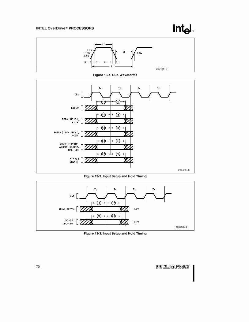
INTEL OverDriveÉ PROCESSORS
290436–7
Figure 13-1. CLK Waveforms
290436–8
Figure 13-2. Input Setup and Hold Timing
290436–9
Figure 13-3. Input Setup and Hold Timing
70
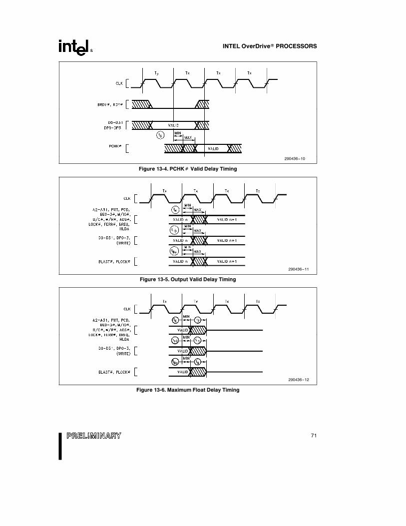
INTEL OverDriveÉ PROCESSORS
290436–10
Figure 13-4. PCHKÝ Valid Delay Timing
290436–11
Figure 13-5. Output Valid Delay Timing
290436–12
Figure 13-6. Maximum Float Delay Timing
71
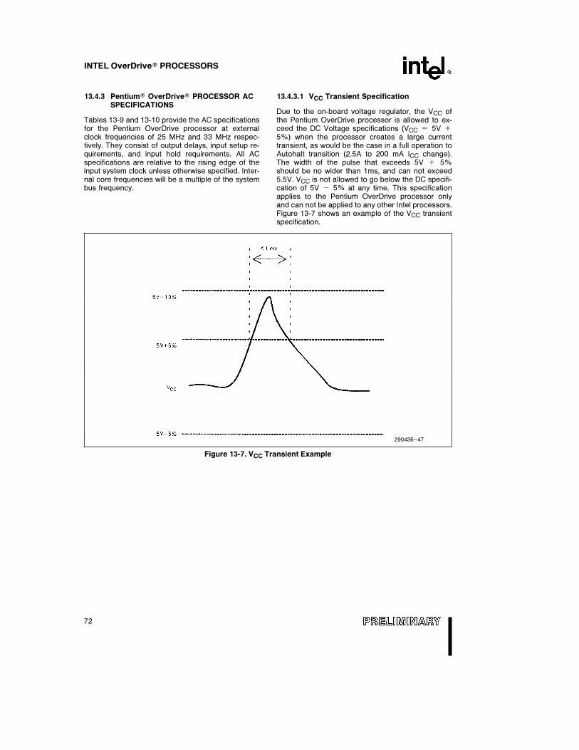
INTEL OverDriveÉ PROCESSORS
13.4.3 PentiumÉ OverDriveÉ PROCESSOR ACSPECIFICATIONS
Tables 13-9 and 13-10 provide the AC specificationsfor the Pentium OverDrive processor at externalclock frequencies of 25 MHz and 33 MHz respec-tively. They consist of output delays, input setup re-quirements, and input hold requirements. All ACspecifications are relative to the rising edge of theinput system clock unless otherwise specified. Inter-nal core frequencies will be a multiple of the systembus frequency.
13.4.3.1 VCC Transient Specification
Due to the on-board voltage regulator, the VCC ofthe Pentium OverDrive processor is allowed to ex-ceed the DC Voltage specifications (VCC e 5V a
5%) when the processor creates a large currenttransient, as would be the case in a full operation toAutohalt transition (2.5A to 200 mA ICC change).The width of the pulse that exceeds 5V a 5%should be no wider than 1ms, and can not exceed5.5V. VCC is not allowed to go below the DC specifi-cation of 5V b 5% at any time. This specificationapplies to the Pentium OverDrive processor onlyand can not be applied to any other Intel processors.Figure 13-7 shows an example of the VCC transientspecification.
290436–47
Figure 13-7. VCC Transient Example
72
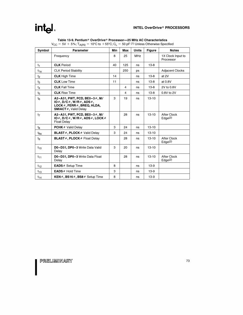
INTEL OverDriveÉ PROCESSORS
Table 13-9. PentiumÉ OverDriveÉ ProcessorÐ25 MHz AC Characteristics
VCC e 5V a 5%; TA(IN) e 10§C to a55§C; CL e 50 pF (1) Unless Otherwise Specified
Symbol Parameter Min Max Units Figure Notes
Frequency 8 25 MHz 1X Clock Input toProcessor
t1 CLK Period 40 125 ns 13-8
t1a CLK Period Stability 250 ps Adjacent Clocks
t2 CLK High Time 14 ns 13-8 at 2V
t3 CLK Low Time 11 ns 13-8 at 0.8V
t4 CLK Fall Time 4 ns 13-8 2V to 0.8V
t5 CLK Rise Time 4 ns 13-8 0.8V to 2V
t6 A2–A31, PWT, PCD, BE0–3Ý, M/ 3 19 ns 13-10IOÝ, D/CÝ, W/RÝ, ADSÝ,LOCKÝ, FERRÝ, BREQ, HLDA,SMIACTÝ, Valid Delay
t7 A2–A31, PWT, PCD, BE0–3Ý, M/ 28 ns 13-10 After ClockIOÝ, D/CÝ, W/RÝ, ADSÝ, LOCKÝ Edge(2)
Float Delay
t8 PCHKÝ Valid Delay 3 24 ns 13-10
t8a BLASTÝ, PLOCKÝ Valid Delay 3 24 ns 13-10
t9 BLASTÝ, PLOCKÝ Float Delay 28 ns 13-10 After ClockEdge(2)
t10 D0–D31, DP0–3 Write Data Valid 3 20 ns 13-10Delay
t11 D0–D31, DP0–3 Write Data Float 28 ns 13-10 After ClockDelay Edge(2)
t12 EADSÝ Setup Time 8 ns 13-9
t13 EADSÝ Hold Time 3 ns 13-9
t14 KENÝ, BS16Ý, BS8Ý Setup Time 8 ns 13-9
73
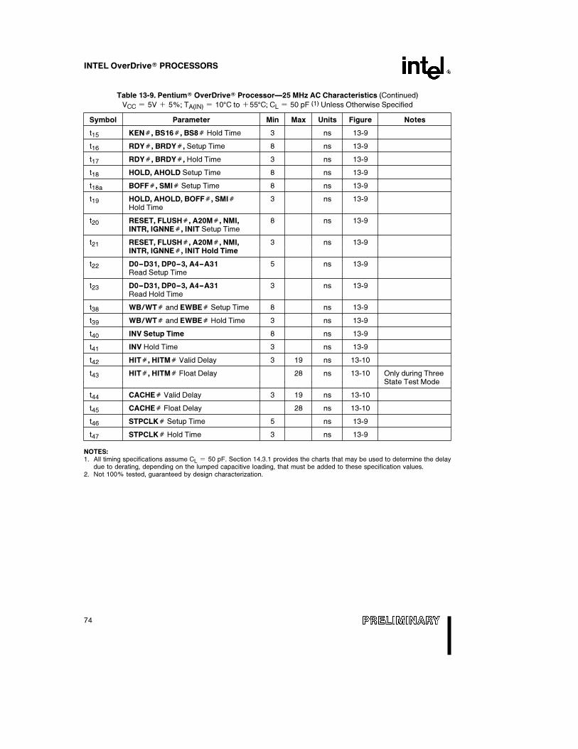
INTEL OverDriveÉ PROCESSORS
Table 13-9. PentiumÉ OverDriveÉ ProcessorÐ25 MHz AC Characteristics (Continued)
VCC e 5V a 5%; TA(IN) e 10§C to a55§C; CL e 50 pF (1) Unless Otherwise Specified
Symbol Parameter Min Max Units Figure Notes
t15 KENÝ, BS16Ý, BS8Ý Hold Time 3 ns 13-9
t16 RDYÝ, BRDYÝ, Setup Time 8 ns 13-9
t17 RDYÝ, BRDYÝ, Hold Time 3 ns 13-9
t18 HOLD, AHOLD Setup Time 8 ns 13-9
t18a BOFFÝ, SMIÝ Setup Time 8 ns 13-9
t19 HOLD, AHOLD, BOFFÝ, SMIÝ 3 ns 13-9Hold Time
t20 RESET, FLUSHÝ, A20MÝ, NMI, 8 ns 13-9INTR, IGNNEÝ, INIT Setup Time
t21 RESET, FLUSHÝ, A20MÝ, NMI, 3 ns 13-9INTR, IGNNEÝ, INIT Hold Time
t22 D0–D31, DP0–3, A4–A31 5 ns 13-9Read Setup Time
t23 D0–D31, DP0–3, A4–A31 3 ns 13-9Read Hold Time
t38 WB/WTÝ and EWBEÝ Setup Time 8 ns 13-9
t39 WB/WTÝ and EWBEÝ Hold Time 3 ns 13-9
t40 INV Setup Time 8 ns 13-9
t41 INV Hold Time 3 ns 13-9
t42 HITÝ, HITMÝ Valid Delay 3 19 ns 13-10
t43 HITÝ, HITMÝ Float Delay 28 ns 13-10 Only during ThreeState Test Mode
t44 CACHEÝ Valid Delay 3 19 ns 13-10
t45 CACHEÝ Float Delay 28 ns 13-10
t46 STPCLKÝ Setup Time 5 ns 13-9
t47 STPCLKÝ Hold Time 3 ns 13-9
NOTES:1. All timing specifications assume CL e 50 pF. Section 14.3.1 provides the charts that may be used to determine the delay
due to derating, depending on the lumped capacitive loading, that must be added to these specification values.2. Not 100% tested, guaranteed by design characterization.
74
INTEL OverDriveÉ PROCESSORS
Table 13-10. PentiumÉ OverDriveÉ ProcessorÐ33 MHz AC Characteristics
VCC e 5V a 5%; TA(IN) e 10§C to a55§C; CL e 50 pF (1) Unless Otherwise Specified
Symbol Parameter Min Max Units Figure Notes
Frequency 8 33 MHz 1X Clock Input toProcessor
t1 CLK Period 30 125 ns 13-8
t1a CLK Period Stability 250 ps Adjacent Clocks
t2 CLK High Time 11 ns 13-8 At 2V
t3 CLK Low Time 8 ns 13-8 At 0.8V
t4 CLK Fall Time 3 ns 13-8 2V to 0.8V
t5 CLK Rise Time 3 ns 13-8 0.8V to 2V
t6 A2–A31, PWT, PCD, BE0–3Ý, 3 14 ns 13-10M/IOÝ, D/CÝ, W/RÝ, ADSÝ,LOCKÝ, FERRÝ, BREQ, HLDA,SMIACTÝ, Valid Delay
t7 A2–A31, PWT, PCD, BE0–3Ý, 20 ns 13-10 After ClockM/IOÝ, D/CÝ, W/RÝ, ADSÝ, Edge(2)
LOCKÝ BP3, BP2, Float Delay
t8 PCHKÝ Valid Delay 3 14 ns 13-10
t8a BLASTÝ, PLOCKÝ Valid Delay 3 14 ns 13-10
t9 BLASTÝ, PLOCKÝ Float Delay 20 ns 13-10 After ClockEdge(2)
t10 D0–D31, DP0–3 Write Data Valid 3 14 ns 13-10Delay
t11 D0–D31, DP0–3 Write Data Float 20 ns 13-10 After ClockDelay Edge(2)
75
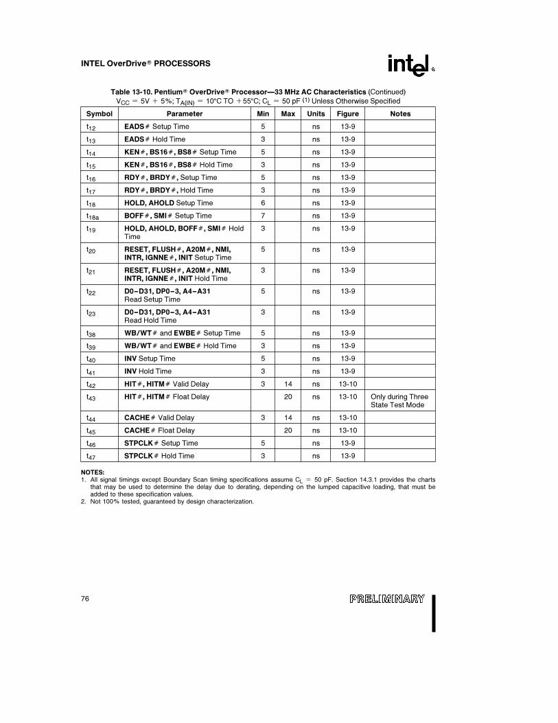
INTEL OverDriveÉ PROCESSORS
Table 13-10. PentiumÉ OverDriveÉ ProcessorÐ33 MHz AC Characteristics (Continued)
VCC e 5V a 5%; TA(IN) e 10§C TO a55§C; CL e 50 pF (1) Unless Otherwise Specified
Symbol Parameter Min Max Units Figure Notes
t12 EADSÝ Setup Time 5 ns 13-9
t13 EADSÝ Hold Time 3 ns 13-9
t14 KENÝ, BS16Ý, BS8Ý Setup Time 5 ns 13-9
t15 KENÝ, BS16Ý, BS8Ý Hold Time 3 ns 13-9
t16 RDYÝ, BRDYÝ, Setup Time 5 ns 13-9
t17 RDYÝ, BRDYÝ, Hold Time 3 ns 13-9
t18 HOLD, AHOLD Setup Time 6 ns 13-9
t18a BOFFÝ, SMIÝ Setup Time 7 ns 13-9
t19 HOLD, AHOLD, BOFFÝ, SMIÝ Hold 3 ns 13-9Time
t20 RESET, FLUSHÝ, A20MÝ, NMI, 5 ns 13-9INTR, IGNNEÝ, INIT Setup Time
t21 RESET, FLUSHÝ, A20MÝ, NMI, 3 ns 13-9INTR, IGNNEÝ, INIT Hold Time
t22 D0–D31, DP0–3, A4–A31 5 ns 13-9Read Setup Time
t23 D0–D31, DP0–3, A4–A31 3 ns 13-9Read Hold Time
t38 WB/WTÝ and EWBEÝ Setup Time 5 ns 13-9
t39 WB/WTÝ and EWBEÝ Hold Time 3 ns 13-9
t40 INV Setup Time 5 ns 13-9
t41 INV Hold Time 3 ns 13-9
t42 HITÝ, HITMÝ Valid Delay 3 14 ns 13-10
t43 HITÝ, HITMÝ Float Delay 20 ns 13-10 Only during ThreeState Test Mode
t44 CACHEÝ Valid Delay 3 14 ns 13-10
t45 CACHEÝ Float Delay 20 ns 13-10
t46 STPCLKÝ Setup Time 5 ns 13-9
t47 STPCLKÝ Hold Time 3 ns 13-9
NOTES:1. All signal timings except Boundary Scan timing specifications assume CL e 50 pF. Section 14.3.1 provides the charts
that may be used to determine the delay due to derating, depending on the lumped capacitive loading, that must beadded to these specification values.
2. Not 100% tested, guaranteed by design characterization.
76
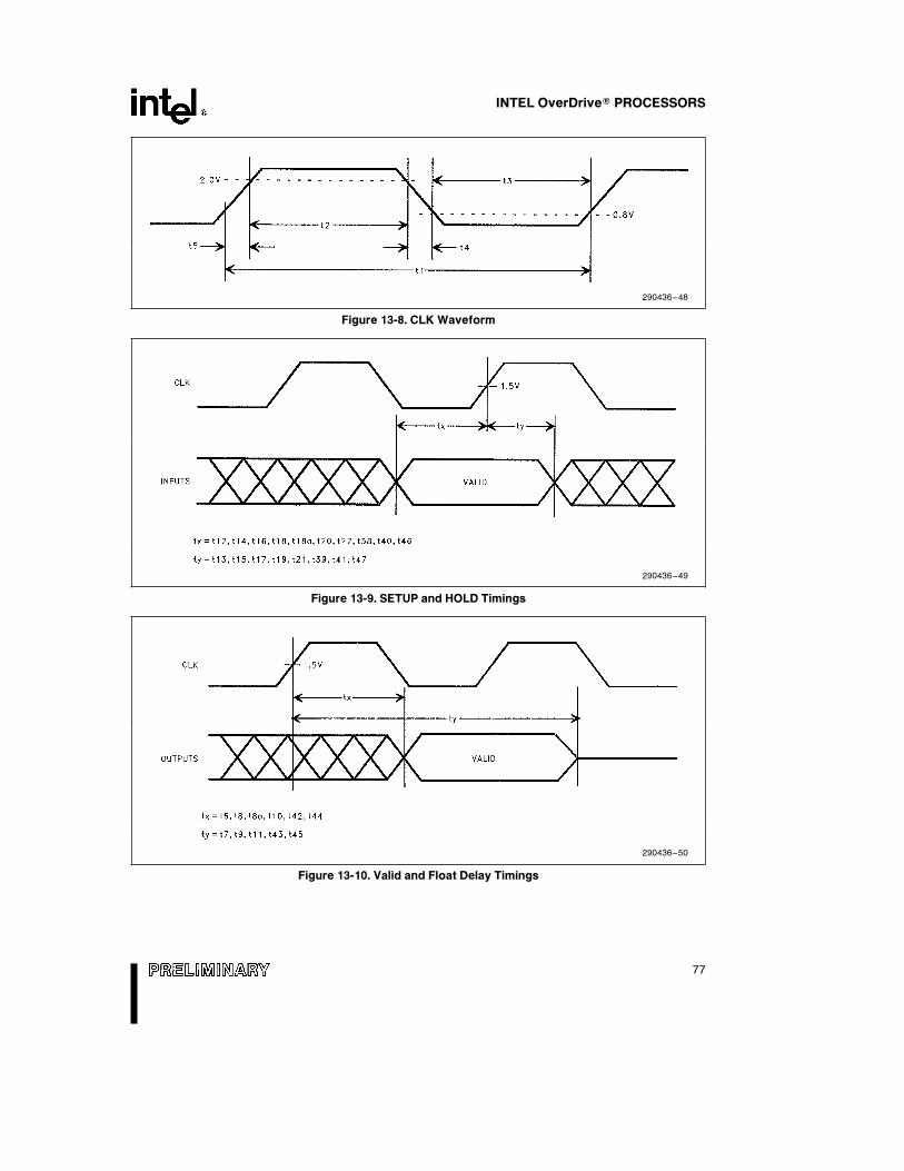
INTEL OverDriveÉ PROCESSORS
290436–48
Figure 13-8. CLK Waveform
290436–49
Figure 13-9. SETUP and HOLD Timings
290436–50
Figure 13-10. Valid and Float Delay Timings
77
INTEL OverDriveÉ PROCESSORS
13.4.3.2 Derating I/O Specifications
Figures 13-11 and 13-12 can be used to determinethe amount of derating necessary for a givenamount of lumped capacitive load. This delay due toderating must be added accordingly to the specifica-tion values listed in Tables 13-9 and 13-10 for thePentium OverDrive processor. These values are de-sign estimates.
Refer to the Pentium Processor Data Book for moreinformation on instruction execution timing and pair-ing.
A generic discussion on the operation of cachememories can be found in the Intel Cache Tutorialavailable from your Intel sales representative or fromIntel’s Literature department, order Ý296543-002.
290436–51
Figure 13-11. Loading Delay vs Load Capacitance (High to Low Transition)
290436–52
Figure 13-12. Loading Delay vs Load Capacitance (Low to High Transition)
78
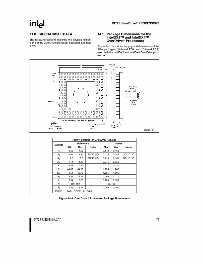
INTEL OverDriveÉ PROCESSORS
14.0 MECHANICAL DATA
The following sections describe the physical dimen-sions of the OverDrive processor packages and heatsinks.
14.1 Package Dimensions for theIntelDX2TM and IntelDX4TM
OverDriveÉ Processors
Figure 14-1 describes the physical dimensions of thePGA packages (168-lead PGA and 169-lead PGA)used with the IntelDX2 and IntelDX4 OverDrive proc-essors.
290436–17
Family: Ceramic Pin Grid Array Package
SymbolMillimeters Inches
Min Max Notes Min Max Notes
A 3.56 4.57 0.140 0.180
A1 0.64 1.14 SOLID LID 0.025 0.045 SOLID LID
A2 2.8 3.5 SOLID LID 0.110 0.140 SOLID LID
A3 1.14 1.40 0.045 0.055
B 0.43 0.51 0.017 0.020
D 44.07 44.83 1.735 1.765
D1 40.51 40.77 1.595 1.605
e1 2.29 2.79 0.090 0.110
L 2.54 3.30 0.100 0.130
N 168, 169 168, 169
S1 1.52 2.54 0.060 0.100
ISSUE IWS REV X 7/15/88
Figure 14-1. OverDriveÉ Processor Package Dimensions
79
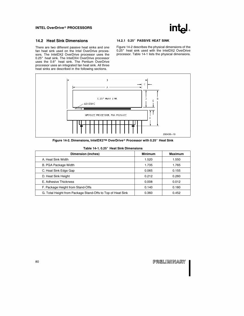
INTEL OverDriveÉ PROCESSORS
14.2 Heat Sink Dimensions
There are two different passive heat sinks and onefan heat sink used on the Intel OverDrive proces-sors. The IntelDX2 OverDrive processor uses the0.25× heat sink. The IntelDX4 OverDrive processoruses the 0.6× heat sink. The Pentium OverDriveprocessor uses an integrated fan heat sink. All threeheat sinks are described in the following sections.
14.2.1 0.25× PASSIVE HEAT SINK
Figure 14-2 describes the physical dimensions of the0.25× heat sink used with the IntelDX2 OverDriveprocessor. Table 14-1 lists the physical dimensions.
290436–19
Figure 14-2. Dimensions, IntelDX2TM OverDriveÉ Processor with 0.25× Heat Sink
Table 14-1. 0.25× Heat Sink Dimensions
Dimension (inches) Minimum Maximum
A. Heat Sink Width 1.520 1.550
B. PGA Package Width 1.735 1.765
C. Heat Sink Edge Gap 0.065 0.155
D. Heat Sink Height 0.212 0.260
E. Adhesive Thickness 0.008 0.012
F. Package Height from Stand-Offs 0.140 0.180
G. Total Height from Package Stand-Offs to Top of Heat Sink 0.360 0.452
80
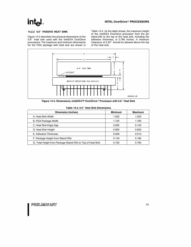
INTEL OverDriveÉ PROCESSORS
14.2.2 0.6× PASSIVE HEAT SINK
Figure 14-3 describes the physical dimensions of the0.6× heat sink used with the IntelDX4 OverDriveprocessors. The maximum and minimum dimensionsfor the PGA package with heat sink are shown in
Table 14-2. As the table shows, the maximum heightof the IntelDX4 OverDrive processor from the pinstand-offs to the top of the heat sink, including theadhesive thickness, is 0.780 inches. A minimumclearance of 0.25× should be allowed above the topof the heat sink.
290436–36
Figure 14-3. Dimensions, IntelDX4TM OverDriveÉ Processor with 0.6× Heat Sink
Table 14-2. 0.6× Heat Sink Dimensions
Dimension (inches) Minimum Maximum
A. Heat Sink Width 1.520 1.550
B. PGA Package Width 1.735 1.765
C. Heat Sink Edge Gap 0.065 0.155
D. Heat Sink Height 0.580 0.600
E. Adhesive Thickness 0.006 0.012
F. Package Height from Stand-Offs 0.140 0.180
G. Total Height from Package Stand-Offs to Top of Heat Sink 0.720 0.780
81
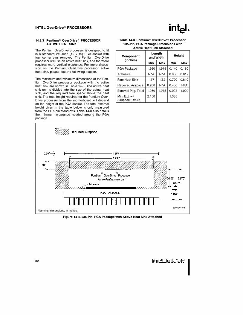
INTEL OverDriveÉ PROCESSORS
14.2.3 PentiumÉ OverDriveÉ PROCESSORACTIVE HEAT SINK
The Pentium OverDrive processor is designed to fitin a standard 240-lead (19 x 19) PGA socket withfour corner pins removed. The Pentium OverDriveprocessor will use an active heat sink, and thereforerequires more vertical clearance. For more discus-sion on the Pentium OverDrive processor activeheat sink, please see the following section.
The maximum and minimum dimensions of the Pen-tium OverDrive processor package with the activeheat sink are shown in Table 14-3. The active heatsink unit is divided into the size of the actual heatsink, and the required free space above the heatsink. The total height required for the Pentium Over-Drive processor from the motherboard will dependon the height of the PGA socket. The total externalheight given in the table below is only measuredfrom the PGA pin stand-offs. Table 14-3 also detailsthe minimum clearance needed around the PGApackage.
Table 14-3. PentiumÉ OverDriveÉ Processor,
235-Pin, PGA Package Dimensions with
Active Heat Sink Attached
Component
(inches)
LengthHeight
and Width
Min Max Min Max
PGA Package 1.950 1.975 0.140 0.180
Adhesive N/A N/A 0.008 0.012
Fan/Heat Sink 1.77 1.82 0.790 0.810
Required Airspace 0.200 N/A 0.400 N/A
External Pkg. Total 1.950 1.975 0.938 1.002
Min. Ext. w/ 2.150 1.338Airspace Fixture
290436–53
*Nominal dimensions, in inches.
Figure 14-4. 235-Pin, PGA Package with Active Heat Sink Attached
82
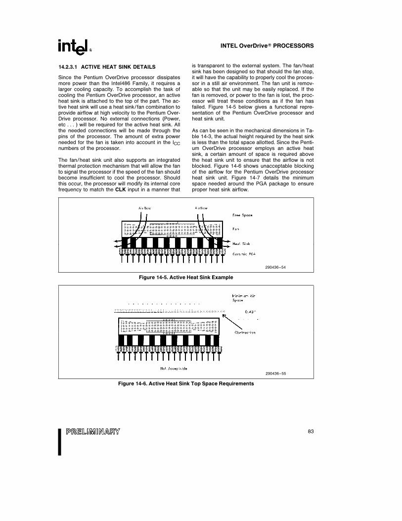
INTEL OverDriveÉ PROCESSORS
14.2.3.1 ACTIVE HEAT SINK DETAILS
Since the Pentium OverDrive processor dissipatesmore power than the Intel486 Family, it requires alarger cooling capacity. To accomplish the task ofcooling the Pentium OverDrive processor, an activeheat sink is attached to the top of the part. The ac-tive heat sink will use a heat sink/fan combination toprovide airflow at high velocity to the Pentium Over-Drive processor. No external connections (Power,etc . . . ) will be required for the active heat sink. Allthe needed connections will be made through thepins of the processor. The amount of extra powerneeded for the fan is taken into account in the ICCnumbers of the processor.
The fan/heat sink unit also supports an integratedthermal protection mechanism that will allow the fanto signal the processor if the speed of the fan shouldbecome insufficient to cool the processor. Shouldthis occur, the processor will modify its internal corefrequency to match the CLK input in a manner that
is transparent to the external system. The fan/heatsink has been designed so that should the fan stop,it will have the capability to properly cool the proces-sor in a still air environment. The fan unit is remov-able so that the unit may be easily replaced. If thefan is removed, or power to the fan is lost, the proc-essor will treat these conditions as if the fan hasfailed. Figure 14-5 below gives a functional repre-sentation of the Pentium OverDrive processor andheat sink unit.
As can be seen in the mechanical dimensions in Ta-ble 14-3, the actual height required by the heat sinkis less than the total space allotted. Since the Penti-um OverDrive processor employs an active heatsink, a certain amount of space is required abovethe heat sink unit to ensure that the airflow is notblocked. Figure 14-6 shows unacceptable blockingof the airflow for the Pentium OverDrive processorheat sink unit. Figure 14-7 details the minimumspace needed around the PGA package to ensureproper heat sink airflow.
290436–54
Figure 14-5. Active Heat Sink Example
290436–55
Figure 14-6. Active Heat Sink Top Space Requirements
83
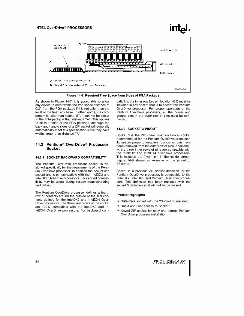
INTEL OverDriveÉ PROCESSORS
290436–56
Figure 14-7. Required Free Space from Sides of PGA Package
As shown in Figure 14-7, it is acceptable to allowany device to enter within the free space distance of0.2× from the PGA package if it is not taller than thelevel of the heat sink base. In other words, if a com-ponent is taller than height ‘‘B’’, it can not be closerto the PGA package than distance ‘‘A’’. This appliesto all four sides of the PGA package, although theback and handle sides of a ZIF socket will generallyautomatically meet this specification since they havewidths larger than distance ‘‘A’’.
14.3 PentiumÉ OverDriveÉ ProcessorSocket
14.3.1 SOCKET BACKWARD COMPATIBILITY
The Pentium OverDrive processor socket is de-signed specifically for the requirements of the Penti-um OverDrive processor. In addition the socket canaccept and is pin compatible with the IntelDX2 andIntelDX4 OverDrive processors. This added compat-ibility may be useful during system troubleshootingand debug.
The Pentium OverDrive processor defines a fourthrow of contacts around the outside of the 169 con-tacts defined for the IntelDX2 and IntelDX4 Over-Drive processors. The three inner rows of the socketare 100% compatible with the IntelDX2 and In-telDX4 OverDrive processors. For backward com-
patibility, the inner row key pin location (E5) must beincluded in any socket that is to accept the PentiumOverDrive processor. For proper operation of thePentium OverDrive processor, all the power andground pins in the outer row of pins must be con-nected.
14.3.2 SOCKET 3 PINOUT
Socket 3 is the ZIF (Zero Insertion Force) socketrecommended for the Pentium OverDrive processor.To ensure proper orientation, four corner pins havebeen removed from the outer row of pins. Additional-ly, the three inner rows of pins are compatible withthe IntelDX2 and IntelDX4 OverDrive processors.This includes the ‘‘key’’ pin in the inside corner.Figure 14-8 shows an example of the pinout ofSocket 3.
Socket 2, a previous ZIF socket definition for thePentium OverDrive processor, is compatible to theIndelDX2, IntelDX4, and Pentium OverDrive proces-sors. This definition has been replaced with thesocket 3 definition so it will not be discussed.
Product Highlights
# Distinctive socket with the ‘‘Socket 3’’ marking
# Rapid end user access to Socket 3
# Keyed ZIF socket for easy and correct PentiumOverDrive processor installation
84
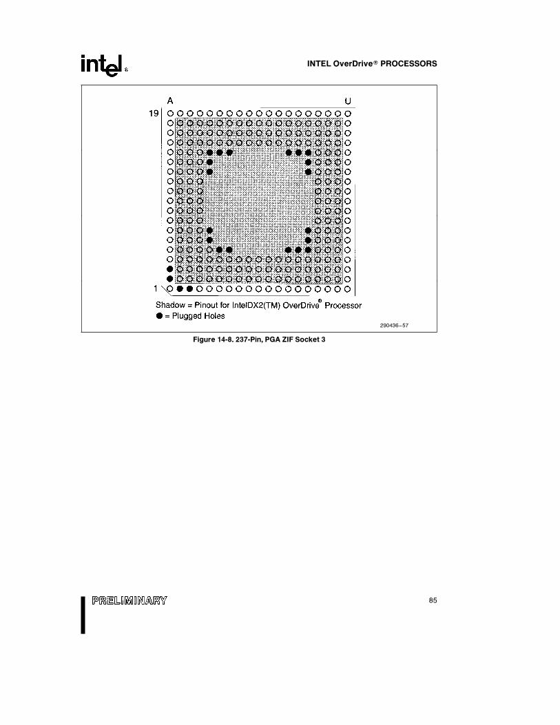
INTEL OverDriveÉ PROCESSORS
290436–57
Figure 14-8. 237-Pin, PGA ZIF Socket 3
85
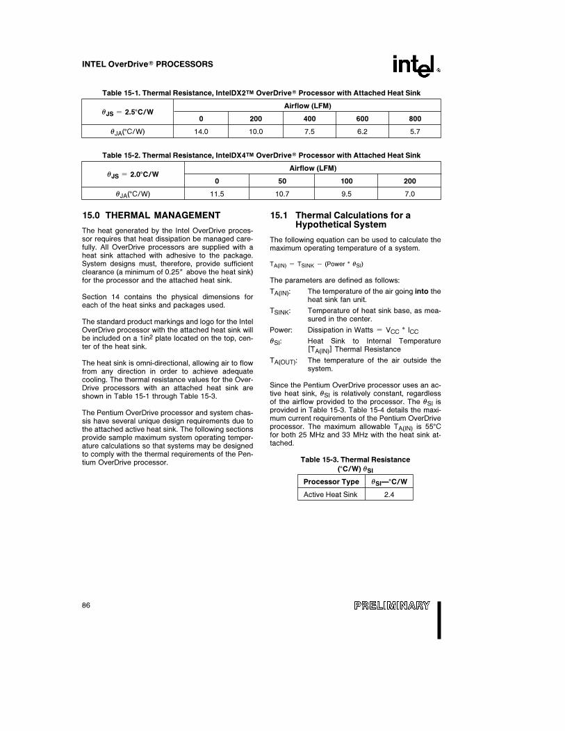
INTEL OverDriveÉ PROCESSORS
Table 15-1. Thermal Resistance, IntelDX2TM OverDriveÉ Processor with Attached Heat Sink
iJS e 2.5§C/WAirflow (LFM)
0 200 400 600 800
iJA(§C/W) 14.0 10.0 7.5 6.2 5.7
Table 15-2. Thermal Resistance, IntelDX4TM OverDriveÉ Processor with Attached Heat Sink
iJS e 2.0§C/WAirflow (LFM)
0 50 100 200
iJA(§C/W) 11.5 10.7 9.5 7.0
15.0 THERMAL MANAGEMENT
The heat generated by the Intel OverDrive proces-sor requires that heat dissipation be managed care-fully. All OverDrive processors are supplied with aheat sink attached with adhesive to the package.System designs must, therefore, provide sufficientclearance (a minimum of 0.25× above the heat sink)for the processor and the attached heat sink.
Section 14 contains the physical dimensions foreach of the heat sinks and packages used.
The standard product markings and logo for the IntelOverDrive processor with the attached heat sink willbe included on a 1in2 plate located on the top, cen-ter of the heat sink.
The heat sink is omni-directional, allowing air to flowfrom any direction in order to achieve adequatecooling. The thermal resistance values for the Over-Drive processors with an attached heat sink areshown in Table 15-1 through Table 15-3.
The Pentium OverDrive processor and system chas-sis have several unique design requirements due tothe attached active heat sink. The following sectionsprovide sample maximum system operating temper-ature calculations so that systems may be designedto comply with the thermal requirements of the Pen-tium OverDrive processor.
15.1 Thermal Calculations for aHypothetical System
The following equation can be used to calculate themaximum operating temperature of a system.
TA(IN) e TSINK b (Power * iSI)
The parameters are defined as follows:
TA(IN): The temperature of the air going into theheat sink fan unit.
TSINK: Temperature of heat sink base, as mea-sured in the center.
Power: Dissipation in Watts e VCC * ICC
iSI: Heat Sink to Internal Temperature[TA(IN)] Thermal Resistance
TA(OUT): The temperature of the air outside thesystem.
Since the Pentium OverDrive processor uses an ac-tive heat sink, iSI is relatively constant, regardlessof the airflow provided to the processor. The iSI isprovided in Table 15-3. Table 15-4 details the maxi-mum current requirements of the Pentium OverDriveprocessor. The maximum allowable TA(IN) is 55§Cfor both 25 MHz and 33 MHz with the heat sink at-tached.
Table 15-3. Thermal Resistance
(§C/W) iSI
Processor Type iSIЧC/W
Active Heat Sink 2.4
86
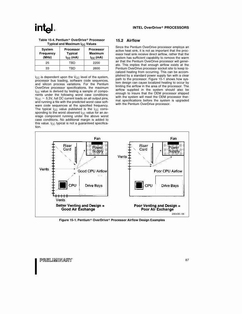
INTEL OverDriveÉ PROCESSORS
Table 15-4. PentiumÉ OverDriveÉ Processor
Typical and Maximum ICC Values
System Processor Processor
Frequency Typical Maximum
(MHz) ICC (mA) ICC (mA)
25 TBD 2200
33 TBD 2600
ICC is dependent upon the VCC level of the system,processor bus loading, software code sequences,and silicon process variations. For the PentiumOverDrive processor specifications, the maximumICC value is derived by testing a sample of compo-nents under the following worst case conditions:VCC e 5.3V, full DC current loads on all output pins,and running a file with the predicted worst case soft-ware code sequences at the specified frequency.The typical ICC value published is the ICC corre-sponding to the worst observed ICC value for an av-erage component running under the above worstcase conditions. No additional margin is added tothis value. ICC typical is not a guaranteed specifica-tion.
15.2 Airflow
Since the Pentium OverDrive processor employs anactive heat sink, it is not as important that the proc-essor heat sink receive direct airflow, rather that thesystem has sufficient capability to remove the warmair that the Pentium OverDrive processor will gener-ate. This implies that enough airflow exists at thePentium OverDrive processor socket site to keep lo-calized heating from occurring. This can be accom-plished by a standard power supply fan with a clearpath to the processor. Figure 15-1 shows how sys-tem design can cause localized heating to occur bylimiting the airflow in the area of the processor. Theairflow supplied in the system should also beenough to insure that the OEM processor shippedwith the system will meet the OEM processor ther-mal specifications before the system is upgradedwith the Pentium OverDrive processor.
290436–58
Figure 15-1. PentiumÉ OverDriveÉ Processor Airflow Design Examples
87

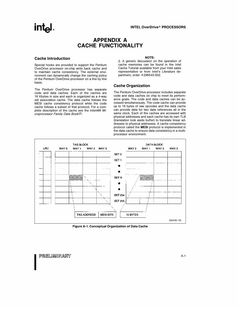
INTEL OverDriveÉ PROCESSORS
APPENDIX ACACHE FUNCTIONALITY
Cache Introduction
Special hooks are provided to support the PentiumOverDrive processor on-chip write back cache andto maintain cache consistency. The external envi-ronment can dynamically change the caching policyof the Pentium OverDrive processor on a line by linebasis.
The Pentium OverDrive processor has separatecode and data caches. Each of the caches are16 Kbytes in size and each is organized as a 4-wayset associative cache. The data cache follows theMESI cache consistency protocol while the codecache follows a subset of that protocol. For a com-plete description of the cache see the Intel486 Mi-croprocessor Family Data Book(2).
NOTE:2. A generic discussion on the operation ofcache memories can be found in the IntelCache Tutorial available from your Intel salesrepresentative or from Intel’s Literature de-partment, order Ý296543-002.
Cache Organization
The Pentium OverDrive processor includes separatecode and data caches on chip to meet its perform-ance goals. The code and data caches can be ac-cessed simultaneously. The code cache can provideup to 16 bytes of raw opcodes and the data cachecan provide data for two data references all in thesame clock. Each of the caches are accessed withphysical addresses and each cache has its own TLB(translation look aside buffer) to translate linear ad-dresses to physical addresses. A cache consistencyprotocol called the MESI protocol is implemented inthe data cache to ensure data consistency in a multi-processor environment.
290436–59
Figure A-1. Conceptual Organization of Data Cache
A-1
INTEL OverDriveÉ PROCESSORS
Each of the caches are 16 Kbytes in size and each isorganized as a 4-way set associative cache. Thereare 256 sets in each cache, each set containing 4lines. Each cache line is 16 bytes wide. Replace-ment in both the data and instruction caches is han-dled by a pseudo LRU mechanism which requiresthree bits per set in each of the caches. A conceptu-al diagram of the organization of the data cache isshown in Figure A-1.
The data cache can support two data referencessimultaneously in one clock, one from each of thetwo pipelines. It is a write back cache with full sup-port for data consistency in a multimaster environ-ment. This is implemented with two status bits asso-ciated with each cache line. The data cache can op-tionally be configured in write through mode on aline by line basis when in write back cache mode.The storage array in the data cache is single portedbut interleaved on 4 byte boundaries to be able toprovide data for two simultaneous accesses to thesame cache line. The tags in the data cache aretriple ported. One of the ports is dedicated to snoop-ing while the other two are used to lookup two inde-pendent addresses corresponding to data refer-ences from each of the pipelines. The code cachetags are also triple ported. Again, one port is dedi-cated to support snooping and other two ports facili-tate split line accesses (simultaneously accessingupper half of one line and lower half of the next line).
The data cache has a 4-way set associative, 64-en-try TLB for 4 KB pages and a separate 4-way setassociative, 8-entry TLB to support 4 MB pages. Thecode cache has one 4-way set associative, 32-entryTLB for 4 KB pages as well as 4 MB pages whichare cached in 4 KB increments. The TLBs associat-ed with the instruction cache are single portedwhereas the data cache TLBs are fully dual portedto be able to translate two independent linear ad-dresses for two data references simultaneously. Re-placement in the TLBs is handled by a pseudo LRUmechanism (similar to the Intel486TM CPU) that re-
quires 3 bits per set. The tag and data arrays of theTLBs are parity protected with a parity bit associatedwith each of the tag and data entries in the TLBs.
State Transition Tables
Lines cached in the Pentium OverDrive processorcan change state because of Pentium OverDriveprocessor generated activity or as a result of activityon the Pentium OverDrive processor bus generatedby other bus masters (snooping). As shown in thefollowing tables, state transitions occur because ofPentium OverDrive processor generated transac-tions (memory reads/writes) and snooping by theexternal system. This protocol has minor differencesfrom the MEI protocol of the Write-Back EnhancedIntelDX2 processor as detailed in Appendix B.
READ CYCLE
The state transitions for the data cache during readsare shown in Table A-1. For a cache line that is inthe M (Modified), E (Exclusive) or S (Shared) states,the data is transferred from the cache to the core,with no bus cycle generated.
Three different cases can occur when a cache readoccurs for an I-state (Invalid) line. An access to aninvalid line indicates a miss in the cache, so a readcycle will be generated. If the CACHEÝ and KENÝpins are sampled low, and WB/WTÝ is high, thenthe line will be stored in the E-state in the cache.WB/WTÝ is sampled with the first BRDYÝ orRDYÝ of the transfer, while KENÝ is sampled oneclock before the first RDYÝ or BRDYÝ. If theCACHEÝ and KENÝ are low, and WB/WTÝ is low,then the cache will be defined as write-through. IfPWT is HIGH, cache line fills will always be storedas shared lines, even if WB/WTÝ is high. This willcause the line to be stored in a S state. If eitherCACHEÝ or KENÝ is high, then the line is non-cacheable, so it will remain in the I state.
A-2
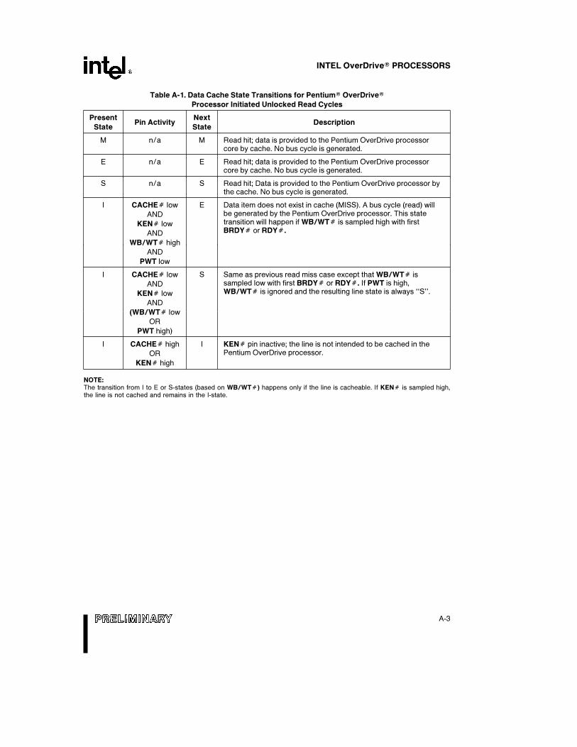
INTEL OverDriveÉ PROCESSORS
Table A-1. Data Cache State Transitions for PentiumÉ OverDriveÉProcessor Initiated Unlocked Read Cycles
PresentPin Activity
NextDescription
State State
M n/a M Read hit; data is provided to the Pentium OverDrive processorcore by cache. No bus cycle is generated.
E n/a E Read hit; data is provided to the Pentium OverDrive processorcore by cache. No bus cycle is generated.
S n/a S Read hit; Data is provided to the Pentium OverDrive processor bythe cache. No bus cycle is generated.
I CACHEÝ low E Data item does not exist in cache (MISS). A bus cycle (read) willbe generated by the Pentium OverDrive processor. This stateANDtransition will happen if WB/WTÝ is sampled high with firstKENÝ lowBRDYÝ or RDYÝ.AND
WB/WTÝ high
AND
PWT low
I CACHEÝ low S Same as previous read miss case except that WB/WTÝ issampled low with first BRDYÝ or RDYÝ. If PWT is high,ANDWB/WTÝ is ignored and the resulting line state is always ‘‘S’’.KENÝ low
AND
(WB/WTÝ low
OR
PWT high)
I CACHEÝ high I KENÝ pin inactive; the line is not intended to be cached in thePentium OverDrive processor.OR
KENÝ high
NOTE:The transition from I to E or S-states (based on WB/WTÝ) happens only if the line is cacheable. If KENÝ is sampled high,the line is not cached and remains in the I-state.
A-3
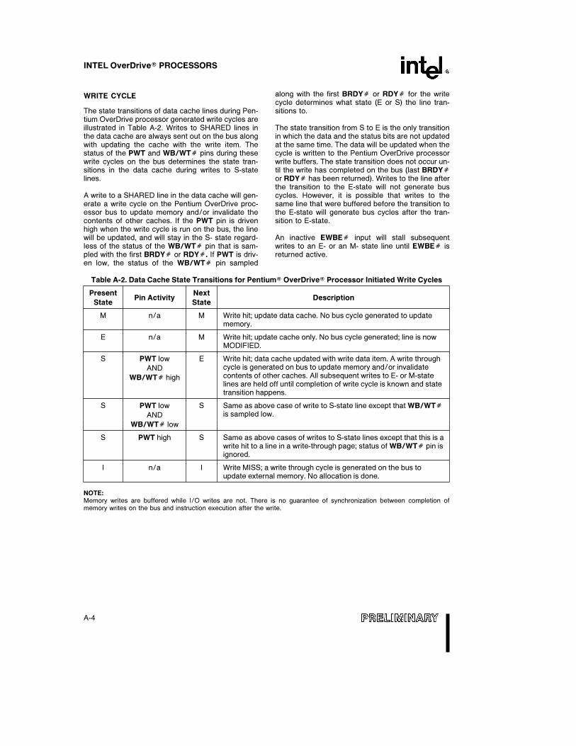
INTEL OverDriveÉ PROCESSORS
WRITE CYCLE
The state transitions of data cache lines during Pen-tium OverDrive processor generated write cycles areillustrated in Table A-2. Writes to SHARED lines inthe data cache are always sent out on the bus alongwith updating the cache with the write item. Thestatus of the PWT and WB/WTÝ pins during thesewrite cycles on the bus determines the state tran-sitions in the data cache during writes to S-statelines.
A write to a SHARED line in the data cache will gen-erate a write cycle on the Pentium OverDrive proc-essor bus to update memory and/or invalidate thecontents of other caches. If the PWT pin is drivenhigh when the write cycle is run on the bus, the linewill be updated, and will stay in the S- state regard-less of the status of the WB/WTÝ pin that is sam-pled with the first BRDYÝ or RDYÝ. If PWT is driv-en low, the status of the WB/WTÝ pin sampled
along with the first BRDYÝ or RDYÝ for the writecycle determines what state (E or S) the line tran-sitions to.
The state transition from S to E is the only transitionin which the data and the status bits are not updatedat the same time. The data will be updated when thecycle is written to the Pentium OverDrive processorwrite buffers. The state transition does not occur un-til the write has completed on the bus (last BRDYÝor RDYÝ has been returned). Writes to the line afterthe transition to the E-state will not generate buscycles. However, it is possible that writes to thesame line that were buffered before the transition tothe E-state will generate bus cycles after the tran-sition to E-state.
An inactive EWBEÝ input will stall subsequentwrites to an E- or an M- state line until EWBEÝ isreturned active.
Table A-2. Data Cache State Transitions for PentiumÉ OverDriveÉ Processor Initiated Write Cycles
PresentPin Activity
NextDescription
State State
M n/a M Write hit; update data cache. No bus cycle generated to updatememory.
E n/a M Write hit; update cache only. No bus cycle generated; line is nowMODIFIED.
S PWT low E Write hit; data cache updated with write data item. A write throughcycle is generated on bus to update memory and/or invalidateANDcontents of other caches. All subsequent writes to E- or M-stateWB/WTÝ highlines are held off until completion of write cycle is known and statetransition happens.
S PWT low S Same as above case of write to S-state line except that WB/WTÝis sampled low.AND
WB/WTÝ low
S PWT high S Same as above cases of writes to S-state lines except that this is awrite hit to a line in a write-through page; status of WB/WTÝ pin isignored.
I n/a I Write MISS; a write through cycle is generated on the bus toupdate external memory. No allocation is done.
NOTE:Memory writes are buffered while I/O writes are not. There is no guarantee of synchronization between completion ofmemory writes on the bus and instruction execution after the write.
A-4
INTEL OverDriveÉ PROCESSORS
INQUIRE CYCLES (SNOOPING)
The purpose of inquire cycles is to check whetherthe address being presented is contained within thecaches in the Pentium OverDrive processor. Inquirecycles may be initiated with or without an invalida-tion request (INV e 1 or 0). The processor samplesthe snoop address during the clock that EADSÝ isactive. An inquire cycle is run through the data andcode caches through a dedicated snoop port to de-termine if the address is contained in one of thePentium OverDrive processor caches. If the addressis in a Pentium OverDrive processor cache, theHITÝ pin is asserted. If the address hits a modifiedline in the processor , the HITMÝ pin is also assert-ed and the modified line is then written back to ex-ternal memory.
Table A-3 shows the state transitions for inquire cy-cles.
Processor Code Cache ConsistencyProtocol
The Pentium OverDrive processor code cache fol-lows a subset of the MESI protocol. Access to linesin the code cache are either a Hit (Shared) or a Miss
(Invalid). In the case of a read hit, the cycle is serv-iced internally to the Pentium OverDrive processorand no bus activity is generated. In the case of aread miss, the read is sent to the external bus andmay be converted to a line fill.
Lines are never overwritten in the code cache.Writes generated by the Pentium OverDrive proces-sor are snooped by the code cache. If there is a hit,the line is invalidated. If there is a miss, no action istaken by the code cache.
Warm Reset Cache Behavior
The INIT pin can be used to reset the Pentium Over-Drive processor without invalidating the on-chipcache. The Pentium OverDrive processor state afterINIT is the same as the state after RESET exceptthat the internal caches, floating point registers, andSMM Base Register retain whatever values they hadprior to recognition of INIT. The INIT signal can beused instead of RESET for warm resets when thecache contents need to be maintained. However,INIT cannot be used in lieu of RESET after powerup. For more information on the INIT and the Penti-um OverDrive processor, please see Section 10.3.
Table A-3. Cache State Transitions during Inquire Cycles
Present Next State Next StateDescription
State INVe1 INVe0
M I S Snoop hit to a MODIFIED line indicated by HITÝ and HITMÝpins low. Pentium OverDrive processor schedules the writingback of the modified line to memory.
E I S Snoop hit indicated by HITÝ pin low; no bus cycle generated.
S I S Snoop hit indicated by HITÝ pin low; no bus cycle generated.
I I I Address not in cache; HITÝ pin high.
A-5

INTEL OverDriveÉ PROCESSORS
APPENDIX BDESIGNING FOR Write-Back Enhanced IntelDX2TM/PentiumÉ OverDriveÉ PROCESSOR COMPATIBILITY
End Users have made upgradability an expectedfeature in any personal computer purchase. ThePentium OverDrive Processor is the intended up-grade for systems based on the Write-Back En-hanced IntelDX2 processor, an IntelDX2 processorwith an on-board write back cache. When installed ina system designed to support a write back proces-sor cache, the Pentium OverDrive processor canreach its full performance potential.
To make the task of designing an upgradable sys-tem easier, the Write-Back Enhanced IntelDX2 andthe Pentium OverDrive processor have been de-signed to be compatible with one another. However,since the Pentium OverDrive processor retains manyof its Pentium processor features, certain system de-sign considerations must be taken into account toensure that a Write-Back Enhanced IntelDX2 proc-essor system can be upgraded seamlessly.
Throughout this section, a ‘‘Single Socket Design’’will refer to a motherboard design that has only oneprocessor site. This means that the Write-Back En-hanced IntelDX2 processor must be removed fromthe socket before the Pentium OverDrive processorcan be installed. A ‘‘Dual Socket Design’’ refers to atwo socket motherboard, one in which the Write-Back Enhanced IntelDX2 resides in a fixed location,and the Pentium OverDrive processor is installedinto an empty upgrade socket. This section willmake reference to both types of designs, but con-centrates on the single socket design strategy.
The following section provides a list of considera-tions that must be examined to allow a PentiumOverDrive processor to operate properly in a systemdesigned to support the Write-Back Enhanced
IntelDX2 processor and a write back processorcache. The considerations listed here are only in-tended to be relevant to the Write-Back EnhancedIntelDX2 processor Enhanced Bus Mode althoughsome may still be valid for the Standard Bus Mode.These considerations are provided as guidelinesonly, and should be used in conjunction with the restof this document to ensure proper Pentium Over-Drive processor operation.
Pinout Differences
The Pentium OverDrive processor pinout is basedon a 19x19 PGA package as opposed to the Write-Back Enhanced IntelDX2 processor 17x17 PGApackage. Most of the signals that are common be-tween the Write-Back Enhanced IntelDX2 processorand the Pentium OverDrive processor exist on thesame pin on both parts (assuming that pin A1 on theWrite-Back Enhanced IntelDX2 processor e Pin B2on the Pentium OverDrive processor).
NOTE:All references to Pentium OverDrive proces-sor pins are with respect to a 19x19 grid,while references to Write-Back EnhancedIntelDX2 processor pins are on a 17x17 grid.
ADDITIONAL PINS ON THE PentiumÉOverDriveÉ PROCESSOR
The Pentium OverDrive processor defines signalpins that provide functionality that the Write-BackEnhanced IntelDX2 processor does not have. Thesepins are defined in Table B-1.
B-1
INTEL OverDriveÉ PROCESSORS
Table B-1. Additional PentiumÉ OverDriveÉ Processor Pins
PentiumÉ OverDriveÉProcessor Pin/
Signal Write-BackComment
Name Enhanced
IntelDX2
Processor Pin
BLENÝ A7/Not Present BLENÝ (Burst Length) controls write bursting on the Pentium(Input) OverDrive processor. It can not be toggled and should be tied high,
low, or left unconnected. It must be driven LOW if the system isable to accept burst write backs. If BLENÝ is driven HIGH to forcewrite backs to be written out as four separate write cycles, HOLDwill not be recognized until all four cycles have completed, eventhough each cycle will have its own ADSÝ and BLASTÝ.
EWBEÝ P1/Not Present EWBEÝ (External Write Buffer Empty) will allow writes to E or M(Input) state lines when asserted LOW. If it is sampled HIGH the
processor will hold off writes to E or M state lines until assertedLOW again.
HITÝ U2/Not Present HITÝ provides an indication that an external snoop has hit a M,E(Output) or S state line in the internal cache.
UPÝ C15/B14 UPÝ is driven LOW to indicate to the system that an upgrade(Output) processor is installed. In a single socket design, it shares a pin with
the Write-Back Enhanced IntelDX2 processor signal, TMS. In adual socket design, it should be connected to the Write-BackEnhanced IntelDX2 processor UPÝ (Input).
Due to its larger package and the ability to consumemore power, the Pentium OverDrive processor alsodefines a number of extra VCC and VSS pins that theWrite-Back Enhanced IntelDX2 processor does notsupport. The extra pins are listed in Table B-2.
Table B-2. Additional VCC and VSS Pins
VCC VSS VSS VCC VSS VSS
A5 U3 K19 G19
A9 A8 U5 L1 H1
A10 A12 U6 L19 H19
A11 A13 U7 R1 M1
A16 A14 U8 R19 M19
D1 A15 U12 U4 N19
D19 A17 U13 U9 Q1
J1 C19 U14 U10 Q19
J19 E1 U15 U11 S1
K1 E19 U17 U16 S19
PINS NOT SUPPORTED BY THE PentiumÉOverDriveÉ PROCESSOR
The Pentium OverDrive processor supports all of thepins on the Write-Back Enhanced IntelDX2 proces-sor except those required for JTAG boundary scanfunctionality and the UPÝ input pin. Single socketdesigns should ensure that if boundary scan fea-tures are implemented, they will not interfere withthe operation of the Pentium OverDrive processor.Dual socket designs should not route the PentiumOverDrive processor into the boundary scan chain.Table B-3 lists the location of the pins that exist onthe Write-Back Enhanced IntelDX2 processor, andthe corresponding different signals on the PentiumOverDrive processor.
B-2

INTEL OverDriveÉ PROCESSORS
Table B-3. Unsupported Write-Back Enhanced IntelDX2 Processor Pins
Write-BackPentiumÉ
EnhancedOverDriveÉ
IntelDX2Processor Comment
ProcessorSignal
SignalName/Pin
Name/Pin
TCK (Input) INC Pin B4 on the Pentium OverDrive processor is defined as an INC pin sothat TCK can be used by the Write-Back Enhanced IntelDX2 processorPin A3 Pin B4in a single socket design without requiring a jumper.
TDI (Input) INC Pin B15 on the Pentium OverDrive processor is defined as an INC pin sothat TDI can be used by the Write-Back Enhanced IntelDX2 processorPin A14 Pin B15in a single socket design without requiring a jumper.
TDO (Output) INC Pin C17 on the Pentium OverDrive processor is defined as an INC pinso that TDO can be used by the Write-Back Enhanced IntelDX2Pin B16 Pin C17processor in a single socket design without requiring a jumper.
TMS (Input) UPÝ (Output) If the Write-Back Enhanced IntelDX2 processor boundary scan featuresare used in a single socket design, the design should ensure that TMSPin B14 Pin C15will not conflict with the Pentium OverDrive processor UPÝ when theupgrade is installed.
UPÝ (Input) INC Pin D12 on the Pentium OverDrive Processor is defined as an INC pinso that there can be no conflict with UPÝ (Input).Pin C11 Pin D12
SHARED SIGNALS LOCATED ON DIFFERENTPINS
There are several signals that the Pentium Over-Drive Processor has in common with the Write-BackEnhanced IntelDX2 processor, but which are locatedon different pins. An example of this would be theHITMÝ signal. On the Pentium OverDrive proces-sor, it is located in the outer row of pins, while on theWrite-Back Enhanced IntelDX2 processor, it is locat-ed on one of the inner row processors. Single socketdesigns require that these signals be tied togetherso that the use of a jumper to reroute the signal isunnecessary. This is done through the use of theINC pin.
INC pins, by definition are ‘‘internally not connected’’and may be used for routing of signals. Certain Pen-tium OverDrive processor INC pins should be con-nected to the signals that correspond to the Write-Back Enhanced IntelDX2 processor write back sig-nals and the SRESET signal. Table B-4 details pinsthat should be routed together. Please note that thelast two columns in Table B-4 are the pins on thePentium OverDrive socket which must be routed to-gether.
Table B-4. Single Socket Compatibility Signals
Write-BackPentiumÉ PentiumÉ
EnhancedOverDriveÉ OverDriveÉ
Signal IntelDX2Processor Processor
ProcessorSignal Pin INC Pins
Signal Pin
INV A10 N1 B11
HITMÝ A12 U1 B13
CACHEÝ B12 G1 C13
WB/WTÝ B13 T1 C14
INIT C10 F19 D11
FERRÝ C14 B14 D15
Figure B-1 shows an example of how the INC pinsshown in Table B-4 should be connected together toallow single socket compatibility between the Write-Back Enhanced IntelDX2 processor and the Penti-um OverDrive processor. The figure is provided asan example only and is not intended to be guide forhow the signals should actually be routed on a moth-erboard.
B-3
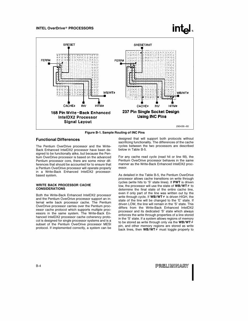
INTEL OverDriveÉ PROCESSORS
290436–60
Figure B-1. Sample Routing of INC Pins
Functional Differences
The Pentium OverDrive processor and the Write-Back Enhanced IntelDX2 processor have been de-signed to be functionally alike, but because the Pen-tium OverDrive processor is based on the advancedPentium processor core, there are some minor dif-ferences that should be accounted for to ensure thata Pentium OverDrive processor will operate properlyin a Write-Back Enhanced IntelDX2 processor-based system.
WRITE BACK PROCESSOR CACHECONSIDERATIONS
Both the Write-Back Enhanced IntelDX2 processorand the Pentium OverDrive processor support an in-ternal write back processor cache. The PentiumOverDrive processor carries over the Pentium proc-essor cache protocol which supports multiple proc-essors in the same system. The Write-Back En-hanced IntelDX2 processor cache coherency proto-col is designed for single processor systems and is asubset of the Pentium OverDrive processor MESIprotocol. If implemented correctly, a system can be
designed that will support both protocols withoutsacrificing functionality. The differences of the cachecycles between the two processors are describedbelow in Table B-5.
For any cache read cycle (read hit or line fill), thePentium OverDrive processor behaves in the samemanner as the Write-Back Enhanced IntelDX2 proc-essor.
As detailed in the Table B-5, the Pentium OverDriveprocessor allows cache transitions on write throughcycles (write hits to ‘S’ state lines). If PWT is drivenlow, the processor will use the state of WB/WTÝ todetermine the final state of the entire cache line,even if only part of the line was written out by thewrite through cycle. If WB/WTÝ is driven HIGH, thestate of the line will be changed to the ‘E’ state. Ifdriven LOW, the line will remain in the ‘S’ state. Thisdiffers from the Write-Back Enhanced IntelDX2processor and its dedicated ‘S’ state which alwaysenforces the write through properties of a line storedin the ‘S’ state. If a system allows regions of memoryto be stored as write through only via the WB/WTÝpin, and other memory regions are stored as writeback lines, then WB/WTÝ must toggle properly to
B-4
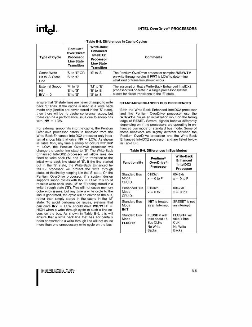
INTEL OverDriveÉ PROCESSORS
Table B-5. Differences in Cache Cycles
PentiumÉ Write-Back
OverDriveÉ Enhanced
Type of Cycle ProcessorIntelDX2
Comments
Line StateProcessor
TransitionLine State
Transition
Cache Write ‘S’ to ‘E’ OR ‘S’ to ‘S’ The Pentium OverDrive processor samples WB/WTÝon write through cycles if PWT is LOW to determineHit to ‘S’ State ‘S’ to ‘S’what kind of transition should occur.Line
External Snoop ‘M’ to ‘S’ ‘M’ to ‘E’ The assumption that a Write-Back Enhanced IntelDX2processor will operate in a single processor systemHit ‘E’ to ‘S’ ‘E’ to ‘E’allows for direct transitions to the ‘E’ state.INV e 0 ‘S’ to ‘S’ ‘S’ to ‘S’
ensure that ‘S’ state lines are never changed to writeback ‘E’ lines. If the cache is used in a write backmode only (linefills are never stored in the ‘S’ state),then there will be no cache coherency issues, butthere can be a performance issue due to snoop hitswith INV e LOW.
For external snoop hits into the cache, the PentiumOverDrive processor differs in behavior from theWrite-Back Enhanced IntelDX2 processor only in ex-ternal snoop hits that drive INV e LOW. As shownin Table 10-5, any time a snoop hit occurs with INVe LOW, the Pentium OverDrive processor willchange the cache line state to ‘S’. The Write-BackEnhanced IntelDX2 processor will allow lines de-fined as write back (‘M’ and ‘E’) to transition to theinitial write back line state of ‘E’. If the line startedout in the ‘S’ state, the Write-Back Enhanced In-telDX2 processor will protect the write throughstatus of the line by keeping it in the ‘S’ state. On thePentium OverDrive processor, if a system designsupports snoop cycles with INV e LOW, this couldresult in write back lines (‘M’ or ‘E’) being stored in awrite through state (‘S’). This will not cause memorycoherency issues, but any time a write cycle to theline is generated, the cycle will be driven to the bus,rather than simply stored in the cache in the ‘M’state. To avoid performance issues, systems thatcan drive INV e LOW should drive WB/WTÝ e
HIGH when a write through cycle to such a line oc-curs on the bus. As shown in Table B-5, this willensure that a write back line that has accidentallybeen converted to a write through line will not causemore than one unnecessary write cycle on the bus.
STANDARD/ENHANCED BUS DIFFERENCES
Both the Write-Back Enhanced IntelDX2 processorand the Pentium OverDrive processor use theWB/WTÝ pin as an initialization input on the fallingedge of RESET. Several signals behave differentlydepending on if the processors are operating in en-hanced bus mode or standard bus mode. Some ofthese behaviors are slightly different between thePentium OverDrive processor and the Write-BackEnhanced IntelDX2 processor, and are listed belowin Table B-6.
Table B-6. Differences in Bus Modes
PentiumÉ Write-Back
Functionality OverDriveÉ Enhanced
ProcessorIntelDX2
Processor
Standard Bus 0153xh 0043xhMode x e 0 to F x e 0 to FCPUID
Enhanced Bus 0153xh 0047xhMode x e 0 to F x e 0 to FCPUID
Standard Bus INIT is treated SRESET is notMode as an Interrupt an interrupt
INIT
Standard Bus FLUSHÝ will FLUSHÝ willMode take about 15 take 1 Bus
Bus CLKs CLKFLUSHÝNo Write No WriteBacks Backs
B-5
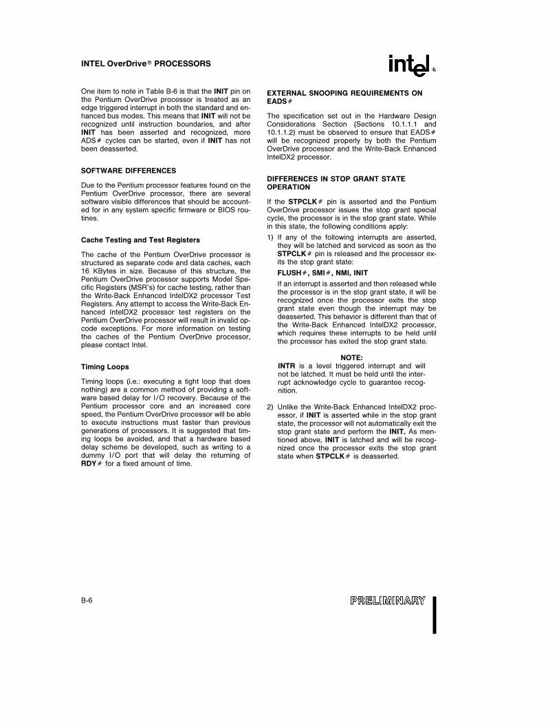
INTEL OverDriveÉ PROCESSORS
One item to note in Table B-6 is that the INIT pin onthe Pentium OverDrive processor is treated as anedge triggered interrupt in both the standard and en-hanced bus modes. This means that INIT will not berecognized until instruction boundaries, and afterINIT has been asserted and recognized, moreADSÝ cycles can be started, even if INIT has notbeen deasserted.
SOFTWARE DIFFERENCES
Due to the Pentium processor features found on thePentium OverDrive processor, there are severalsoftware visible differences that should be account-ed for in any system specific firmware or BIOS rou-tines.
Cache Testing and Test Registers
The cache of the Pentium OverDrive processor isstructured as separate code and data caches, each16 KBytes in size. Because of this structure, thePentium OverDrive processor supports Model Spe-cific Registers (MSR’s) for cache testing, rather thanthe Write-Back Enhanced IntelDX2 processor TestRegisters. Any attempt to access the Write-Back En-hanced IntelDX2 processor test registers on thePentium OverDrive processor will result in invalid op-code exceptions. For more information on testingthe caches of the Pentium OverDrive processor,please contact Intel.
Timing Loops
Timing loops (i.e.: executing a tight loop that doesnothing) are a common method of providing a soft-ware based delay for I/O recovery. Because of thePentium processor core and an increased corespeed, the Pentium OverDrive processor will be ableto execute instructions must faster than previousgenerations of processors. It is suggested that tim-ing loops be avoided, and that a hardware baseddelay scheme be developed, such as writing to adummy I/O port that will delay the returning ofRDYÝ for a fixed amount of time.
EXTERNAL SNOOPING REQUIREMENTS ONEADSÝ
The specification set out in the Hardware DesignConsiderations Section (Sections 10.1.1.1 and10.1.1.2) must be observed to ensure that EADSÝwill be recognized properly by both the PentiumOverDrive processor and the Write-Back EnhancedIntelDX2 processor.
DIFFERENCES IN STOP GRANT STATEOPERATION
If the STPCLKÝ pin is asserted and the PentiumOverDrive processor issues the stop grant specialcycle, the processor is in the stop grant state. Whilein this state, the following conditions apply:
1) If any of the following interrupts are asserted,they will be latched and serviced as soon as theSTPCLKÝ pin is released and the processor ex-its the stop grant state:
FLUSHÝ, SMIÝ, NMI, INIT
If an interrupt is asserted and then released whilethe processor is in the stop grant state, it will berecognized once the processor exits the stopgrant state even though the interrupt may bedeasserted. This behavior is different than that ofthe Write-Back Enhanced IntelDX2 processor,which requires these interrupts to be held untilthe processor has exited the stop grant state.
NOTE:INTR is a level triggered interrupt and willnot be latched. It must be held until the inter-rupt acknowledge cycle to guarantee recog-nition.
2) Unlike the Write-Back Enhanced IntelDX2 proc-essor, if INIT is asserted while in the stop grantstate, the processor will not automatically exit thestop grant state and perform the INIT. As men-tioned above, INIT is latched and will be recog-nized once the processor exits the stop grantstate when STPCLKÝ is deasserted.
B-6