Embed Size (px)
Citation preview
AAllmmaa MMaatteerr SSttuuddiioorruumm –– UUnniivveerrssiittàà ddii BBoollooggnnaa
DOTTORATO DI RICERCA IN
INGENGERIA ELETTRONICA, INFORMATICA E DELLE TELECOMUNICAZIONI
Ciclo XXVII
Settore Concorsuale di afferenza: 09/E3 Settore Scientifico disciplinare: ING-INF/01
MANY-CORE ARCHITECTURES: HARDWARE-SOFTWARE OPTIMIZATION AND MODELING TECHNIQUES
Presentata da: Christian Pinto
Coordinatore Dottorato Relatore
Prof. Alessandro Vanelli Coralli Prof. Luca Benini
Esame finale anno 2015
Many-Core Architectures:
Hardware-Software Optimization and
Modeling Techniques
Christian Pinto
Dept. of Electrical, Electronic and Information Engineering (DEI)
University of Bologna
A thesis submitted for the degree of
Doctor of Philosophy
2015

Abstract
During the last few decades an unprecedented technological growth has been
at the center of the embedded systems design paramount, with Moore’s Law being
the leading factor of this trend. Today in fact an ever increasing number of cores
can be integrated on the same die, marking the transition from state-of-the-art
multi-core chips to the new many-core design paradigm. Such many-core chips
aim is twofold: provide high computing performance, and increase the energy ef-
ficiency of the hardware in terms of OPS/Watt. Despite the extraordinarily high
computing power, the complexity of many-core chips opens the door to several
challenges. First of all, as a result of the increased silicon density of modern
Systems-on-a-Chip (SoC), the design space exploration needed to find the best
design has exploded. Hardware designers are in fact facing the problem of a huge
design space, with an extremely high number of possibilities to be explored to
make a comprehensive evaluation of each of their architectural choices. This is
also exacerbated by the extremely competitive silicon market, forcing each actor
to always shrink the time-to-market of products to be ahead of the competitors.
Virtual Platforms have always been used to enable hardware-software co-design,
but today they are facing with the huge complexity of both hardware and soft-
ware systems. In this thesis two different research works on Virtual Platforms
are presented: the first one is intended for the hardware developer, to easily al-
low complex cycle accurate simulations of many-core SoCs. The second work
exploits the parallel computing power of off-the-shelf General Purpose Graphics
Processing Units (GPGPUs), with the goal of an increased simulation speed.
The term Virtualization can be used in the context of many-core systems
not only to refer to the aforementioned hardware emulation tools (Virtual Plat-
forms), but also to identify parallel programming aid tools and the higher level
virtualization techniques used today to create software instances of computing
systems [21]. Virtualization can be used in fact for two other main purposes: 1)
to help the programmer to achieve the maximum possible performance of an ap-
plication, by hiding the complexity of the underlying hardware. 2) to efficiently
exploit the high parallel hardware of many-core chips in environments with mul-
tiple active Virtual Machines, in which the accelerator might be able to sustain
multiple execution requests from different virtual machines. In this last context
beside the sharing of the accelerator, isolation between different virtual machines
is required. This thesis is focused on virtualization techniques with the goal to
mitigate, and overtake when possible, some of the challenges introduced by the
many-core design paradigm.
Beside the design challenge, many-core chips themselves pose some challenges
to programmers in order to effectively exploit their theoretical computing power.
The most important and performance affecting is the Memory-Bandwidth Bottle-
neck : as a result of several design choices most many-core chips are composed by
multi-core computing clusters, which are replicated over the design. Such design
pattern is aimed at reducing the design effort, by just defining the architecture of
a single cluster and then deploying several clusters on the same chip. For the sake
of area/power efficiency, processing elements in a cluster are often not equipped
with data cache memories, but rather they share an on-chip data scratch-pad
memory. On-chip memories are usually fast but available in limited amount, and
the data-set of an application can not always fit into. For this reason data are
usually allocated in the much ample, but way slower, external memory. To mit-
igate the external-memory access latency, and due to the lack of a data cache,
programmers are forced to apply copy-in/copy-out schemes to move chunks of
data from the external memory to the on-chip memory (and vice versa). Such
programming patterns usually exploit a Direct Memory Access Engine (DMA en-
gine) to overlap the computation of a chunk of data with the copy of the next. In
this thesis a memory virtualization infrastructure is presented, aimed at automat-
ically dealing with external-memory-to-scratch-pad transfers. The virtualization
framework treats the on-chip scratch-pad of a computing cluster as if it was a
cache (Software Cache), and data is moved back and forth from external mem-
ory without the intervention of the programmer. The software cache is also able
to deal with multiple concurrent accesses from the processing element of each
cluster.
The last aspect investigated is virtualization at its higher level of abstraction,
used in the domain of servers/cloud computing to create sand-boxed instances
of operating systems (Virtual Machines) physically sharing the same hardware
(hardware consolidation). Such type of virtualization has recently been made
available also in the embedded systems domain, thanks to the advent of hardware
assisted virtualization in ARM based processors [15]. In a virtualized system each
hardware peripheral needs to have its virtual counterpart, to give each virtual
machine the idea of a dedicated computing device. Since many-core chips are
used as a co-processor (Accelerators) to general purpose multi-core processors
(Host), they also need to be virtualized and made available to all the virtual
machines running on the system. However modern many-core based systems
are still under constant refinement, and current virtualization techniques are not
able to overcome some of the architectural limitations. One of these limitations
is memory sharing between host and accelerator. General purpose processors
usually handle any memory region under virtual memory, giving a flexible and
contiguous view of the physical memory even if data is not contiguously allocated.
This goal is achieved by using a Memory Management Unit (MMU). On the other
hand many-core chips are only able to access contiguously physical memory, being
them not equipped with an MMU. This makes impossible for the co-processor
to directly access any data buffer created from the host system. The problem of
memory sharing is much more effective in a virtualized environment, where the
accelerator could be sharing data with different virtual machines. This challenge
is addressed in this thesis with the definition of a virtualization transparently
enabling host-accelerator memory sharing, and implementing a resources sharing
mechanism enabling the many-core accelerator to be used concurrently by several
virtual machines.
To my Family and Vanessa for their unconditional support, trust
and love during these years.
Contents
Contents i
List of Figures v
List of Tables ix
1 Introduction 1
1.1 Thesis Contribution and Organization . . . . . . . . . . . . . . . 5
1.2 Many-core architectures . . . . . . . . . . . . . . . . . . . . . . . 7
1.2.1 Cluster Architecture: Relevant Examples . . . . . . . . . . 9
1.2.1.1 ST Microelectronics P2012/STHORM . . . . . . 9
1.2.1.2 Plurality HAL - Hypercore Architecture Line . . 11
1.2.1.3 Kalray MPPA MANYCORE . . . . . . . . . . . 12
2 VirtualSoC: a Virtual Platform for Design Space Exploration 15
2.1 Overview . . . . . . . . . . . . . . . . . . . . . . . . . . . . . . . . 15
2.2 Related work . . . . . . . . . . . . . . . . . . . . . . . . . . . . . 18
2.3 Target Architecture . . . . . . . . . . . . . . . . . . . . . . . . . . 20
2.4 Many-core Accelerator . . . . . . . . . . . . . . . . . . . . . . . . 21
2.5 Host-Accelerator Interface . . . . . . . . . . . . . . . . . . . . . . 25
2.6 Simulation Software Support . . . . . . . . . . . . . . . . . . . . . 27
2.7 Evaluation . . . . . . . . . . . . . . . . . . . . . . . . . . . . . . . 28
2.7.1 Experimental Setup . . . . . . . . . . . . . . . . . . . . . . 28
2.7.2 VirtualSoC Use Cases . . . . . . . . . . . . . . . . . . . . 28
i
CONTENTS
2.8 Conclusions . . . . . . . . . . . . . . . . . . . . . . . . . . . . . . 31
3 GP-GPU based Acceleration of Virtual Platforms 33
3.1 Overview . . . . . . . . . . . . . . . . . . . . . . . . . . . . . . . . 33
3.2 Related Work . . . . . . . . . . . . . . . . . . . . . . . . . . . . . 35
3.3 Target architecture . . . . . . . . . . . . . . . . . . . . . . . . . . 38
3.4 The Fermi GPU Architecture and CUDA . . . . . . . . . . . . . . 39
3.4.1 Key Implementative Issues for Performance . . . . . . . . 40
3.5 Full Simulation Flow . . . . . . . . . . . . . . . . . . . . . . . . . 41
3.5.1 Instruction Set Simulator . . . . . . . . . . . . . . . . . . . 42
3.5.2 Cache Simulator . . . . . . . . . . . . . . . . . . . . . . . 44
3.5.2.1 Communication buffers . . . . . . . . . . . . . . . 46
3.5.3 Network-on-Chip Simulator . . . . . . . . . . . . . . . . . 47
3.6 Experimental Results . . . . . . . . . . . . . . . . . . . . . . . . . 50
3.6.1 Simulation time breakdown . . . . . . . . . . . . . . . . . 50
3.6.2 Simulator Performance Evaluation . . . . . . . . . . . . . 52
3.6.3 Comparison with OVPSim . . . . . . . . . . . . . . . . . . 55
3.7 Conclusions . . . . . . . . . . . . . . . . . . . . . . . . . . . . . . 58
4 Memory Virtualization: Software Caches 61
4.1 Overview . . . . . . . . . . . . . . . . . . . . . . . . . . . . . . . . 61
4.2 Related work . . . . . . . . . . . . . . . . . . . . . . . . . . . . . 65
4.3 Implementation . . . . . . . . . . . . . . . . . . . . . . . . . . . . 68
4.3.1 Software cache data structures . . . . . . . . . . . . . . . . 68
4.3.2 Logic implementation . . . . . . . . . . . . . . . . . . . . . 69
4.3.2.1 Lookup function . . . . . . . . . . . . . . . . . . 69
4.3.2.2 Miss Handling routine . . . . . . . . . . . . . . . 70
4.3.3 Concurrency management . . . . . . . . . . . . . . . . . . 71
4.3.4 Direct-mapped vs set-associative software cache . . . . . . 73
4.4 Object Oriented caching extensions . . . . . . . . . . . . . . . . . 74
4.4.1 Objects of arbitrary size . . . . . . . . . . . . . . . . . . . 77
4.4.2 Programmer Interface . . . . . . . . . . . . . . . . . . . . 78
ii
CONTENTS
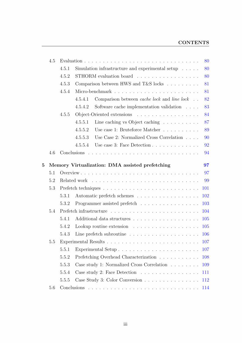
4.5 Evaluation . . . . . . . . . . . . . . . . . . . . . . . . . . . . . . . 80
4.5.1 Simulation infrastructure and experimental setup . . . . . 80
4.5.2 STHORM evaluation board . . . . . . . . . . . . . . . . . 80
4.5.3 Comparison between HWS and T&S locks . . . . . . . . . 81
4.5.4 Micro-benchmark . . . . . . . . . . . . . . . . . . . . . . . 81
4.5.4.1 Comparison between cache lock and line lock . . 82
4.5.4.2 Software cache implementation validation . . . . 83
4.5.5 Object-Oriented extensions . . . . . . . . . . . . . . . . . 84
4.5.5.1 Line caching vs Object caching . . . . . . . . . . 87
4.5.5.2 Use case 1: Bruteforce Matcher . . . . . . . . . . 89
4.5.5.3 Use Case 2: Normalized Cross Correlation . . . . 90
4.5.5.4 Use case 3: Face Detection . . . . . . . . . . . . . 92
4.6 Conclusions . . . . . . . . . . . . . . . . . . . . . . . . . . . . . . 94
5 Memory Virtualization: DMA assisted prefetching 97
5.1 Overview . . . . . . . . . . . . . . . . . . . . . . . . . . . . . . . . 97
5.2 Related work . . . . . . . . . . . . . . . . . . . . . . . . . . . . . 99
5.3 Prefetch techniques . . . . . . . . . . . . . . . . . . . . . . . . . . 101
5.3.1 Automatic prefetch schemes . . . . . . . . . . . . . . . . . 102
5.3.2 Programmer assisted prefetch . . . . . . . . . . . . . . . . 103
5.4 Prefetch infrastructure . . . . . . . . . . . . . . . . . . . . . . . . 104
5.4.1 Additional data structures . . . . . . . . . . . . . . . . . . 105
5.4.2 Lookup routine extension . . . . . . . . . . . . . . . . . . 105
5.4.3 Line prefetch subroutine . . . . . . . . . . . . . . . . . . . 106
5.5 Experimental Results . . . . . . . . . . . . . . . . . . . . . . . . . 107
5.5.1 Experimental Setup . . . . . . . . . . . . . . . . . . . . . . 107
5.5.2 Prefetching Overhead Characterization . . . . . . . . . . . 108
5.5.3 Case study 1: Normalized Cross Correlation . . . . . . . . 109
5.5.4 Case study 2: Face Detection . . . . . . . . . . . . . . . . 111
5.5.5 Case Study 3: Color Conversion . . . . . . . . . . . . . . . 112
5.6 Conclusions . . . . . . . . . . . . . . . . . . . . . . . . . . . . . . 114
iii
CONTENTS
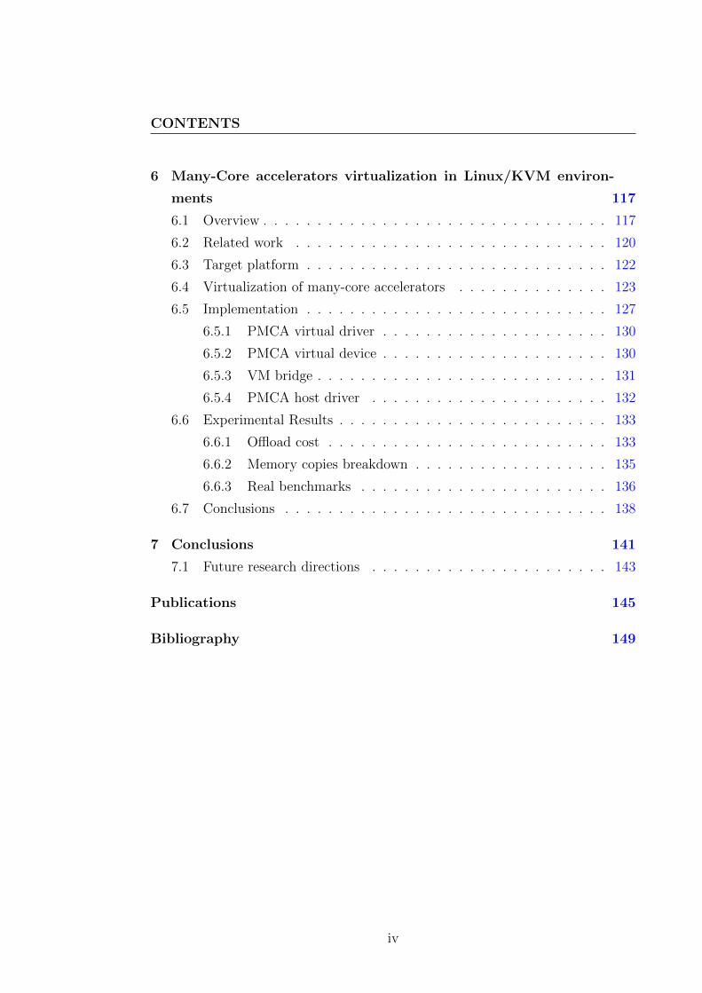
6 Many-Core accelerators virtualization in Linux/KVM environ-
ments 117
6.1 Overview . . . . . . . . . . . . . . . . . . . . . . . . . . . . . . . . 117
6.2 Related work . . . . . . . . . . . . . . . . . . . . . . . . . . . . . 120
6.3 Target platform . . . . . . . . . . . . . . . . . . . . . . . . . . . . 122
6.4 Virtualization of many-core accelerators . . . . . . . . . . . . . . 123
6.5 Implementation . . . . . . . . . . . . . . . . . . . . . . . . . . . . 127
6.5.1 PMCA virtual driver . . . . . . . . . . . . . . . . . . . . . 130
6.5.2 PMCA virtual device . . . . . . . . . . . . . . . . . . . . . 130
6.5.3 VM bridge . . . . . . . . . . . . . . . . . . . . . . . . . . . 131
6.5.4 PMCA host driver . . . . . . . . . . . . . . . . . . . . . . 132
6.6 Experimental Results . . . . . . . . . . . . . . . . . . . . . . . . . 133
6.6.1 Offload cost . . . . . . . . . . . . . . . . . . . . . . . . . . 133
6.6.2 Memory copies breakdown . . . . . . . . . . . . . . . . . . 135
6.6.3 Real benchmarks . . . . . . . . . . . . . . . . . . . . . . . 136
6.7 Conclusions . . . . . . . . . . . . . . . . . . . . . . . . . . . . . . 138
7 Conclusions 141
7.1 Future research directions . . . . . . . . . . . . . . . . . . . . . . 143
Publications 145
Bibliography 149
iv
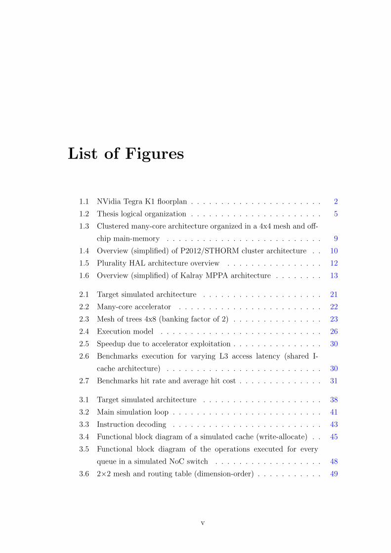
List of Figures
1.1 NVidia Tegra K1 floorplan . . . . . . . . . . . . . . . . . . . . . . 2
1.2 Thesis logical organization . . . . . . . . . . . . . . . . . . . . . . 5
1.3 Clustered many-core architecture organized in a 4x4 mesh and off-
chip main-memory . . . . . . . . . . . . . . . . . . . . . . . . . . 9
1.4 Overview (simplified) of P2012/STHORM cluster architecture . . 10
1.5 Plurality HAL architecture overview . . . . . . . . . . . . . . . . 12
1.6 Overview (simplified) of Kalray MPPA architecture . . . . . . . . 13
2.1 Target simulated architecture . . . . . . . . . . . . . . . . . . . . 21
2.2 Many-core accelerator . . . . . . . . . . . . . . . . . . . . . . . . 22
2.3 Mesh of trees 4x8 (banking factor of 2) . . . . . . . . . . . . . . . 23
2.4 Execution model . . . . . . . . . . . . . . . . . . . . . . . . . . . 26
2.5 Speedup due to accelerator exploitation . . . . . . . . . . . . . . . 30
2.6 Benchmarks execution for varying L3 access latency (shared I-
cache architecture) . . . . . . . . . . . . . . . . . . . . . . . . . . 30
2.7 Benchmarks hit rate and average hit cost . . . . . . . . . . . . . . 31
3.1 Target simulated architecture . . . . . . . . . . . . . . . . . . . . 38
3.2 Main simulation loop . . . . . . . . . . . . . . . . . . . . . . . . . 41
3.3 Instruction decoding . . . . . . . . . . . . . . . . . . . . . . . . . 43
3.4 Functional block diagram of a simulated cache (write-allocate) . . 45
3.5 Functional block diagram of the operations executed for every
queue in a simulated NoC switch . . . . . . . . . . . . . . . . . . 48
3.6 2×2 mesh and routing table (dimension-order) . . . . . . . . . . . 49
v
LIST OF FIGURES
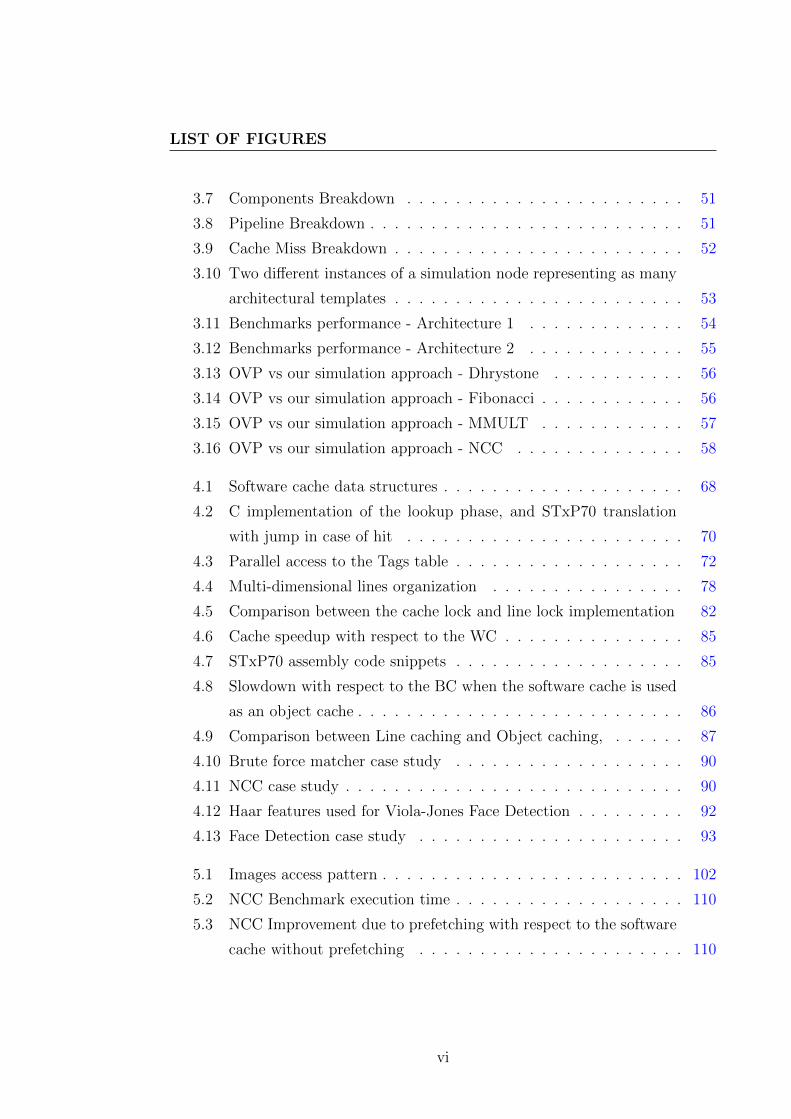
3.7 Components Breakdown . . . . . . . . . . . . . . . . . . . . . . . 51
3.8 Pipeline Breakdown . . . . . . . . . . . . . . . . . . . . . . . . . . 51
3.9 Cache Miss Breakdown . . . . . . . . . . . . . . . . . . . . . . . . 52
3.10 Two different instances of a simulation node representing as many
architectural templates . . . . . . . . . . . . . . . . . . . . . . . . 53
3.11 Benchmarks performance - Architecture 1 . . . . . . . . . . . . . 54
3.12 Benchmarks performance - Architecture 2 . . . . . . . . . . . . . 55
3.13 OVP vs our simulation approach - Dhrystone . . . . . . . . . . . 56
3.14 OVP vs our simulation approach - Fibonacci . . . . . . . . . . . . 56
3.15 OVP vs our simulation approach - MMULT . . . . . . . . . . . . 57
3.16 OVP vs our simulation approach - NCC . . . . . . . . . . . . . . 58
4.1 Software cache data structures . . . . . . . . . . . . . . . . . . . . 68
4.2 C implementation of the lookup phase, and STxP70 translation
with jump in case of hit . . . . . . . . . . . . . . . . . . . . . . . 70
4.3 Parallel access to the Tags table . . . . . . . . . . . . . . . . . . . 72
4.4 Multi-dimensional lines organization . . . . . . . . . . . . . . . . 78
4.5 Comparison between the cache lock and line lock implementation 82
4.6 Cache speedup with respect to the WC . . . . . . . . . . . . . . . 85
4.7 STxP70 assembly code snippets . . . . . . . . . . . . . . . . . . . 85
4.8 Slowdown with respect to the BC when the software cache is used
as an object cache . . . . . . . . . . . . . . . . . . . . . . . . . . . 86
4.9 Comparison between Line caching and Object caching, . . . . . . 87
4.10 Brute force matcher case study . . . . . . . . . . . . . . . . . . . 90
4.11 NCC case study . . . . . . . . . . . . . . . . . . . . . . . . . . . . 90
4.12 Haar features used for Viola-Jones Face Detection . . . . . . . . . 92
4.13 Face Detection case study . . . . . . . . . . . . . . . . . . . . . . 93
5.1 Images access pattern . . . . . . . . . . . . . . . . . . . . . . . . . 102
5.2 NCC Benchmark execution time . . . . . . . . . . . . . . . . . . . 110
5.3 NCC Improvement due to prefetching with respect to the software
cache without prefetching . . . . . . . . . . . . . . . . . . . . . . 110
vi
LIST OF FIGURES
5.4 Face Detection execution time normalized to a DMA hand-tuned
implementation . . . . . . . . . . . . . . . . . . . . . . . . . . . . 110
5.5 Face Detection miss reduction percentage . . . . . . . . . . . . . . 110
5.6 Color conversion execution time normalized to DMA hand-tuned
implementation . . . . . . . . . . . . . . . . . . . . . . . . . . . . 112
6.1 Target platform high level view . . . . . . . . . . . . . . . . . . . 122
6.2 Accelerator’s partitions assigned to different applications . . . . . 124
6.3 Example of application offloading a kernel to the accelerator . . . 125
6.4 Memory handling in presence of an IOMMU (left side), and in
absence of IOMMU (right side) . . . . . . . . . . . . . . . . . . . 125
6.5 Virtualization infrastructure overview . . . . . . . . . . . . . . . . 126
6.6 Task offload descriptor . . . . . . . . . . . . . . . . . . . . . . . . 128
6.7 Data copies performed . . . . . . . . . . . . . . . . . . . . . . . . 129
6.8 Flow of the offload descriptor through the virtualization infrastruc-
ture . . . . . . . . . . . . . . . . . . . . . . . . . . . . . . . . . . 129
6.9 Offload cost . . . . . . . . . . . . . . . . . . . . . . . . . . . . . . 133
6.10 a) Breakdown of the constant component of the offload time. b)
Breakdown of the copy time when 128 KB of data are copied . . . 134
6.11 Distribution of memory copies over the total execution time of
benchmarks . . . . . . . . . . . . . . . . . . . . . . . . . . . . . . 136
6.12 Execution time over multiple iterations, normalized to (offload
time + memory copies) . . . . . . . . . . . . . . . . . . . . . . . . 137
vii
LIST OF FIGURES
viii
List of Tables
2.1 Experimental Setup . . . . . . . . . . . . . . . . . . . . . . . . . . 29
3.1 Cache design parameters . . . . . . . . . . . . . . . . . . . . . . . 44
3.2 Benchmarks scaled-up datasets . . . . . . . . . . . . . . . . . . . 54
4.1 Comparison between T&S and HWS locks . . . . . . . . . . . . . 81
5.1 Prefetch overhead added to the lookup function, each cell contains:
#instructions / #clock cycles (line size 32 bytes) . . . . . . . 107
6.1 Benchmarks details . . . . . . . . . . . . . . . . . . . . . . . . . . 136
ix

x
Chapter 1
Introduction
The advent of many-core architectures has profoundly changed the panorama of
both hardware and software design. Embedded systems today are rapidly moving
from small homogeneous systems with few powerful computing units, towards the
much complex heterogeneous Multi-Processor Systems on Chip (MPSoC) embed-
ding on the same die several small computing units. The increasing number of
computing units allows embedded systems to be exploited for workloads usually
tailored for workstation or high performance computing, representative examples
are Machine Vision and Scientific Computation [3].
Energy efficiency in terms of OPS/Watt is the most influencing factor for an
embedded system design, with the future target to provide 100 GOPS within
the power envelope of 1W [129]. Heterogeneity is used as a key tool to increase
the energy efficiency of a MPSoC and sustain the disruptive computing power
delivered by such systems, by staying within an always shrinking market-driven
power budget. Various design schemes are available today: systems composed
by a combination of powerful and energy efficient cores [81], and also designs
exploiting various types of specialized or general purpose parallel accelerators [96,
134]. The combination of different types of computing units allows the system to
adapt to different workloads, providing computing power when running complex
tasks or running on the more energy efficient cores when the performance is not
required. And finally offloading computation to an accelerator, when high parallel
1
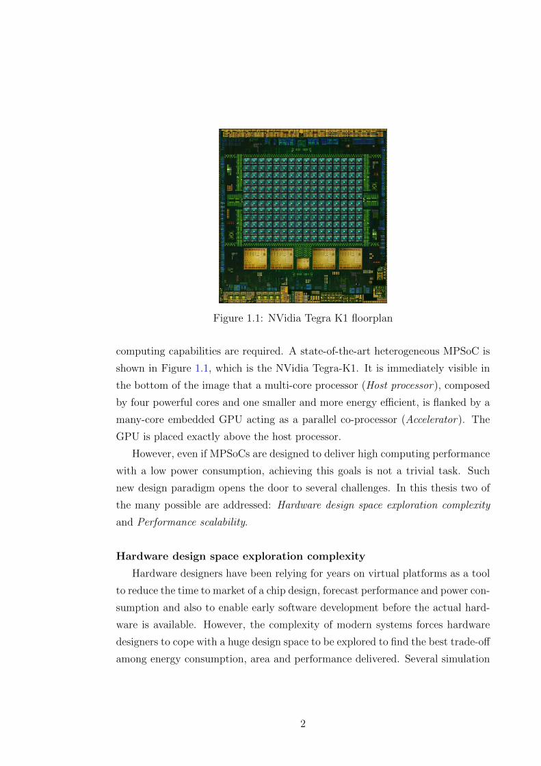
Figure 1.1: NVidia Tegra K1 floorplan
computing capabilities are required. A state-of-the-art heterogeneous MPSoC is
shown in Figure 1.1, which is the NVidia Tegra-K1. It is immediately visible in
the bottom of the image that a multi-core processor (Host processor), composed
by four powerful cores and one smaller and more energy efficient, is flanked by a
many-core embedded GPU acting as a parallel co-processor (Accelerator). The
GPU is placed exactly above the host processor.
However, even if MPSoCs are designed to deliver high computing performance
with a low power consumption, achieving this goals is not a trivial task. Such
new design paradigm opens the door to several challenges. In this thesis two of
the many possible are addressed: Hardware design space exploration complexity
and Performance scalability.
Hardware design space exploration complexity
Hardware designers have been relying for years on virtual platforms as a tool
to reduce the time to market of a chip design, forecast performance and power con-
sumption and also to enable early software development before the actual hard-
ware is available. However, the complexity of modern systems forces hardware
designers to cope with a huge design space to be explored to find the best trade-off
among energy consumption, area and performance delivered. Several simulation
2
frameworks are available today off-the-shelf [24, 29, 75, 77, 84, 87, 126, 136], but
almost all of them suffer of three main problems, which make them not suitable
to model a complex MPSoC:
1. Lack of models for deep micro-architectural components: hardware designs
with more than hundreds of computing units use various architectural com-
ponents, to allow efficient and scalable communication between cores (e.g.
Networks-On-Chip) and complex memory hierarchies. Such components
have to be modeled at the micro-architectural level to enable accurate power
estimations and performance measurements.
2. Lack of support for Full System simulation: modern MPSoCs are composed
by a Host processor and one or more accelerators. The host processor is
usually in charge of executing an operating system (e.g. Linux), while the
accelerators are used as a co-processors to speedup the execution of com-
putationally heavy tasks. In this scenario the interaction between host
processor and accelerators, being it a memory transfer or a synchroniza-
tion, may have a significant effect on applications performance. Virtual
platforms have to accurately model such interactions to enable precise ap-
plication profiling.
3. Sequential simulation: most of the available modeling tools are relying on
a sequential execution model, in which all components of the design are
simulated in sequence by a single application thread. In the near future
MPSoCs will feature thousand of computing units, and such a modeling
technique will make the simulation time of a reasonable application to be
to slow for practical use.
Performance scalability
Even if Pollack’s rule sates that the increase of performance is proportional
to the square root of the increase in complexity of a system, achieving such per-
formance is not a trivial task. Programmers seeking for applications performance
3
are thus obliged to know architectural specific details, and apply complex pro-
gramming patterns to adapt their applications to the specific target hardware.
One of the most performance affective problems is the memory wall [133],
which is due to a huge gap in the technological advance between CPU and memory
speed. An efficient utilization of the memory hierarchy is thus critical for perfor-
mance, especially in a system with thousand of cores where the required memory
bandwidth can be extremely high. However due to some design choices taken for
the sake of area and power consumption reduction, the hardware is not always
able to automatically fill the gap of memory latency. One example is the choice
to substitute data caches with scratchpad memories, because the latter with the
same size in bytes occupies 30% less area than a cache [20]. Programmers can not
rely anymore on data caches to hide the external memory access latency, and try
to overlap as much as possible computation with communication. One common
programming pattern is DMA double buffering, in which computation is divided
in chunks and while the actual is computed the next one is read from external
memory. Such type of design choice forces application programmers to know deep
hardware related features to boost the performance of their code, leading often
to complex and error-prone programming. A software runtime is presented in
this thesis which automatically handles external-memory-to-scratchpad memory
transfers, without any intervention of the programmer.
Another design related challenge is memory sharing between host processor
and many-core accelerator. A general purpose processor, when running an op-
erating system, uses a virtual memory abstraction to handle the whole physical
memory available on a platform. This is possible thanks to a Memory Man-
agement Unit (MMU), which is in charge to translate any virtual address to its
equivalent in physical memory. State-of-the-art many-core accelerators are often
not equipped with an MMU [101, 104], meaning that only physical memory ad-
dresses can be used from within the accelerator. In a typical application the Host
processor acting as a master is in charge of handling the main application flow,
and input/output data buffers shared with the accelerator are created under the
virtual memory abstraction. Since most many-core accelerators are only able to
4
Virtualiza on
Virtual
Pla"orms
System
tools
Sequen al
Micro-architectural
Level
(Chapter 2)
Parallel fast
Emula on
(Chapter 3)
Hardware details
abstrac on
(Chapters 4-5)
System
virtualiza on
(Chapter 6)
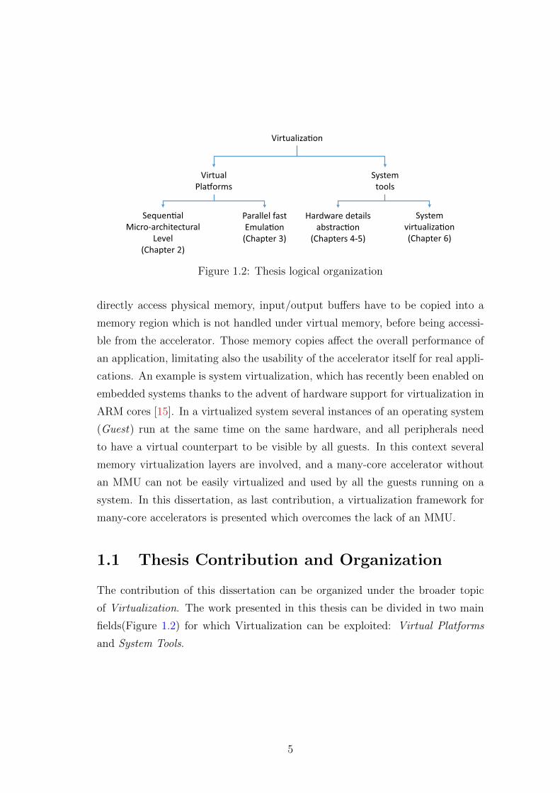
Figure 1.2: Thesis logical organization
directly access physical memory, input/output buffers have to be copied into a
memory region which is not handled under virtual memory, before being accessi-
ble from the accelerator. Those memory copies affect the overall performance of
an application, limitating also the usability of the accelerator itself for real appli-
cations. An example is system virtualization, which has recently been enabled on
embedded systems thanks to the advent of hardware support for virtualization in
ARM cores [15]. In a virtualized system several instances of an operating system
(Guest) run at the same time on the same hardware, and all peripherals need
to have a virtual counterpart to be visible by all guests. In this context several
memory virtualization layers are involved, and a many-core accelerator without
an MMU can not be easily virtualized and used by all the guests running on a
system. In this dissertation, as last contribution, a virtualization framework for
many-core accelerators is presented which overcomes the lack of an MMU.
1.1 Thesis Contribution and Organization
The contribution of this dissertation can be organized under the broader topic
of Virtualization. The work presented in this thesis can be divided in two main
fields(Figure 1.2) for which Virtualization can be exploited: Virtual Platforms
and System Tools.
5
Virtual Platforms: used for design space exploration and early software
development, are a virtual representation of an hardware system which can be
modeled at different levels of abstraction. In particular in this thesis in Chapter
2 is presented VirtualSoC, a SystemC [7] based virtual platform. VirtualSoC
can perform the full system simulation of MPSoCs, where the host processor is
modeled by QEMU [25] and a many-core accelerator is completely written in
SystemC. The focus of this virtual platform is on the many-core accelerator and
its interaction with the host processor. In particular it is possible to model at
the micro-architectural level various on-chip interconnection mediums, memories,
instruction and data caches and computing units. The models used are heavily
configurable to perform an exhaustive design space exploration, and allow also
to perform performance and power analyses based on user provided models. In
Chapter 3 the simulation of large systems is addressed, presenting the internals
of a tool for parallel simulation (SIMinG-1k) exploiting commodity hardware like
GP-GPUs. SIMinG-1k is able to model a many-core system with up to 4096 com-
puting units (ARM and X86 ISA) connected using an On Chip Network(NoC),
and sharing a common memory hierarchy organized under the PGAS 1 scheme.
SIMinG-1k can be used for the design of parallel programming models and high
level design space exploration.
System tools: Virtualization can be considered a system tool when used to
ease the work of programmers, by abstracting hardware details of the platform,
enclosing them in a higher level (virtual) representation. It can also be considered
a system tool when talking of system virtualization, where several instances of
an operating system run indistinctly on the same hardware and all have the view
of dedicated (virtual) hardware system. In this dissertation in Chapter 4 and
Chapter 5 is presented a memory virtualization framework targeting STHORM
[88], a cluster based many-core accelerators with on chip scratchpad data mem-
ories. The framework is able to automatically handle the on-chip scratchpad
memory in each cluster as a data cache (Software Cache), relieving the program-
1PGAS: Partitioned Global Address Space, which assumes a global memory address spacethat is logically partitioned among all the computing nodes in the system
6
mer from the task of hiding the external memory access latency. Since each
computing cluster is composed by 16 processors, the software cache runtime is
able to orchestrate parallel accesses to a shared cache structure exploiting the
hardware synchronization facilities provided by the STHORM chip. Moreover a
DMA-based prefetching extension is presented with the aim of further mitigating
the external memory access latency. Chapter 6 is focused on system virtualiza-
tion. We present a framework for the virtualization of IOMMU-less many-core
accelerator, which enables the virtualization of many-core chips in Linux/KVM
environments. Beside the actual sharing of the many-core accelerator among dif-
ferent virtual machines, the framework presented is also able to overcome the
problem of memory sharing with the Host processor, thanks to a fully-software
memory sharing subsystem. It is demonstrated in the chapter that even in ab-
sence of an MMU, a many-core accelerator can be still utilized to obtain concrete
benefits in terms of application speedup.
Finally, in Chapter 7 the dissertation is concluded summarizing the main
results obtained by this research work.
1.2 Many-core architectures
Several variants of many-core architectures have been designed and are in use for
years now. As a matter of fact, since the mid 2000s we observed the integration
of an increasing number of cores onto a single integrated circuit die, known as
a Chip Multi-Processor (CMP) or Multi-Processor System-on-Chip (MPSoC), or
onto multiple dies in a single chip package. Manufacturers still leverage Moore’s
Law [92] (doubling of the number of transistors on chip every 18 months), but
business as usual is not an option anymore: scaling performance by increasing
clock frequency and instruction throughput of single cores, the trend for electronic
systems in the last 30 years, has proved to be not viable anymore [11, 31, 52]. As a
consequence, computing systems moved to multi-core1 designs and subsequently,
1For clarity, the multi-core term is intended for platforms with 2 to few tens cores, whilewith many-core we refer to systems with tens to hundreds of cores. The distinction is not rigid
7
thanks to the integration density, to the many-core era where energy-efficient
performance scaling is achieved by exploiting large-scale parallelism, rather than
speeding up the single processing units [11, 31, 52, 76].
Such trend can be found in a wide spectrum of platforms, ranging from general
purpose computing, high-performance to the embedded world.
In the general purpose domain we observed the first multi-core processors al-
most a decade ago. Intel core duo [55] and Sony-Toshiba-IBM (STI) Cell Broad-
band Engine [71] are notable examples of this paradigm shift. The trend did
not stop and nowadays we have in this segment many-core examples such as the
TILE-Gx8072 processor, comprising seventy-two cores operating at frequencies
up to 1.2 GHz [40]. Instead, when performance is the primary requisite of the ap-
plication domain, we can cite several notable architectures such as Larrabee [115]
for visual computing, the research microprocessors Intel’s SCC [68] and Tera-
scale project [130] and, more recently, Intel’s Xeon Phi [63]. In the embedded
world, we are observing today a proliferation of many-core heterogeneous plat-
forms. The so-called asymmetric of heterogeneous design features many small,
energy-efficient cores integrated with a full-blown processor. Its is emerging as
the main trend in the embedded domain, since it represents the most flexible and
efficient design paradigm. Notable examples of such architectures are the AMD
Accelerated Processing Units [33], Nvidia TEGRA family [96], STMicroelectron-
ics P2012/STHORM [27] or Kalray’s many-core processors [72].
The work presented in this thesis is focused on the embedded domain where,
more than in other areas, modern high-end applications are asking for increasingly
stringent and irreconcilable requirements. An outstanding example consist of the
mobile market. As highlighted in [129], the digital workload of a smartphone
(all control, data and signal processing) amounts to nearly 100 Giga Operations
Per Second (GOPS) with a power-budget of 1 Watt. Moreover, workload re-
quirements increase at a steady rate, roughly by an order of magnitude every 5
years.
From the architectural point of view, with the evolution from tens of cores to
and throughout the dissertation, the terms multi-core and many-core may be used indistinctly.
8
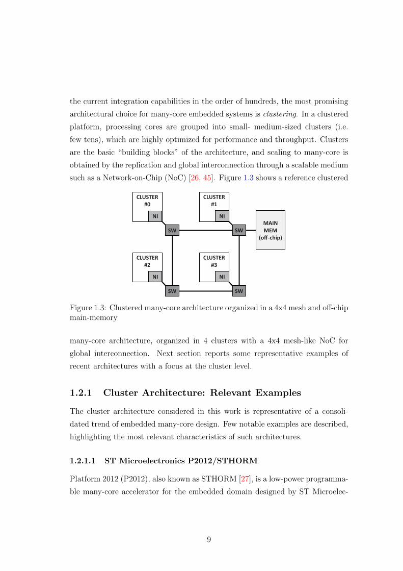
the current integration capabilities in the order of hundreds, the most promising
architectural choice for many-core embedded systems is clustering. In a clustered
platform, processing cores are grouped into small- medium-sized clusters (i.e.
few tens), which are highly optimized for performance and throughput. Clusters
are the basic “building blocks” of the architecture, and scaling to many-core is
obtained by the replication and global interconnection through a scalable medium
such as a Network-on-Chip (NoC) [26, 45]. Figure 1.3 shows a reference clustered
CLUSTER
#0
NI
SW
CLUSTER
#1
NI
SW
CLUSTER
#2
NI
SW
CLUSTER
#3
NI
SW
MAIN
MEM
(off-chip)
Figure 1.3: Clustered many-core architecture organized in a 4x4 mesh and off-chipmain-memory
many-core architecture, organized in 4 clusters with a 4x4 mesh-like NoC for
global interconnection. Next section reports some representative examples of
recent architectures with a focus at the cluster level.
1.2.1 Cluster Architecture: Relevant Examples
The cluster architecture considered in this work is representative of a consoli-
dated trend of embedded many-core design. Few notable examples are described,
highlighting the most relevant characteristics of such architectures.
1.2.1.1 ST Microelectronics P2012/STHORM
Platform 2012 (P2012), also known as STHORM [27], is a low-power programma-
ble many-core accelerator for the embedded domain designed by ST Microelec-
9
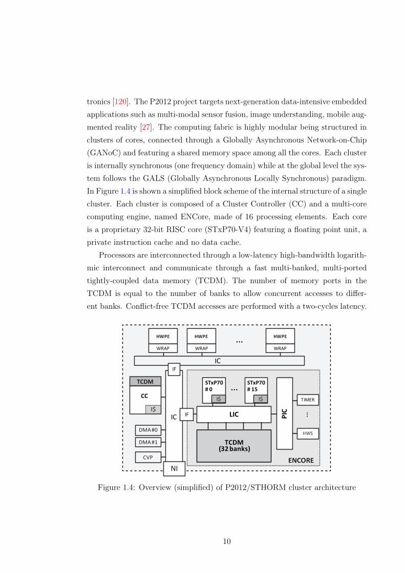
tronics [120]. The P2012 project targets next-generation data-intensive embedded
applications such as multi-modal sensor fusion, image understanding, mobile aug-
mented reality [27]. The computing fabric is highly modular being structured in
clusters of cores, connected through a Globally Asynchronous Network-on-Chip
(GANoC) and featuring a shared memory space among all the cores. Each cluster
is internally synchronous (one frequency domain) while at the global level the sys-
tem follows the GALS (Globally Asynchronous Locally Synchronous) paradigm.
In Figure 1.4 is shown a simplified block scheme of the internal structure of a single
cluster. Each cluster is composed of a Cluster Controller (CC) and a multi-core
computing engine, named ENCore, made of 16 processing elements. Each core
is a proprietary 32-bit RISC core (STxP70-V4) featuring a floating point unit, a
private instruction cache and no data cache.
Processors are interconnected through a low-latency high-bandwidth logarith-
mic interconnect and communicate through a fast multi-banked, multi-ported
tightly-coupled data memory (TCDM). The number of memory ports in the
TCDM is equal to the number of banks to allow concurrent accesses to differ-
ent banks. Conflict-free TCDM accesses are performed with a two-cycles latency.
ENCORE
TCDM(32 banks)
DMA #0
STxP70
# 15…TIMER
HWS
STxP70
# 0
I$CC
I$
TCDM
IC
DMA #1
HWPE
WRAP
HWPE
WRAP
HWPE
WRAP
IC
…
IF
NI
IF LIC PIC
CVP
I$
…
Figure 1.4: Overview (simplified) of P2012/STHORM cluster architecture
10
The logarithmic interconnect consists of fully combinatorial Mesh-of-Trees (MoT)
interconnection network. Data routing is based on address decoding: a first-stage
checks if the requested address falls within the TCDM address range or has to be
directed off-cluster. The interconnect provides fine-grained address interleaving
on the memory banks to reduce banking conflicts in case of multiple accesses to
logically contiguous data structures. If no bank conflicts arise, data routing is
done in parallel for each core. In case of conflicting requests, a round-robin based
scheduler coordinates accesses to memory banks in a fair manner. Banking con-
flicts result in higher latency, depending on the number of concurrent conflicting
accesses. Each cluster is equipped with a Hardware Synchronizer (HWS) which
provides low-level services such as semaphores, barriers, and event propagation
support, two DMA engines, and a Clock Variability and Power (CVP) module.
The cluster template can be enhanced with application specific hardware pro-
cessing elements (HWPEs), to accelerate key functionalities in hardware. They
are interconnected to the ENCore with an asynchronous local interconnect (LIC).
The first release of P2012 (STHORM) features 4 homogeneous clusters for a total
of 69 cores and a software stack based on two programming models, namely a
component-based Native Programming Model (NPM) and OpenCL-based [121]
(named CLAM - CL Above Many-Cores) while OpenMP [42] support is under
development.
1.2.1.2 Plurality HAL - Hypercore Architecture Line
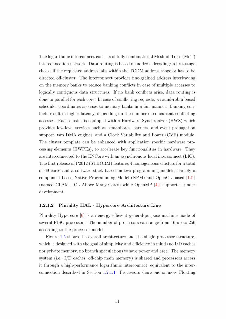
Plurality Hypercore [6] is an energy efficient general-purpose machine made of
several RISC processors. The number of processors can range from 16 up to 256
according to the processor model.
Figure 1.5 shows the overall architecture and the single processor structure,
which is designed with the goal of simplicity and efficiency in mind (no I/D caches
nor private memory, no branch speculation) to save power and area. The memory
system (i.e., I/D caches, off-chip main memory) is shared and processors access
it through a high-performance logarithmic interconnect, equivalent to the inter-
connection described in Section 1.2.1.1. Processors share one or more Floating
11
Scheduling NoC
Scheduler
CORE
CORE
CORE
…
FPU FPU
SharedAccelerators
Shared Memory
NoC
…
…
…
…
Scheduler IF
PC
ALU
Register
Register
Register
Memory IF
Figure 1.5: Plurality HAL architecture overview
Point Units, and one or more shared hardware accelerators can be embedded in
the design. This platform can be programmed with a task-oriented programming
model, where the so-called “agents” are specified with a proprietary language.
Tasks are efficiently dispatched by a scheduler/synchronizer called Central Syn-
chronizer Unit (CSU), which also ensures workload balancing.
1.2.1.3 Kalray MPPA MANYCORE
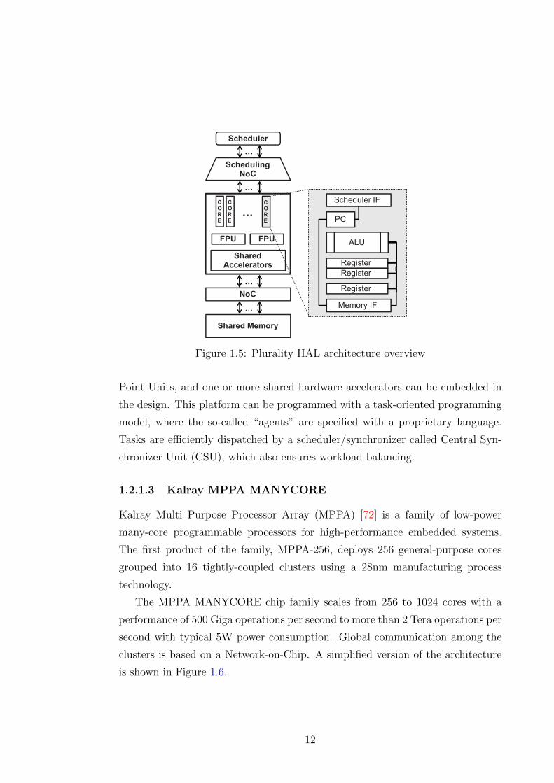
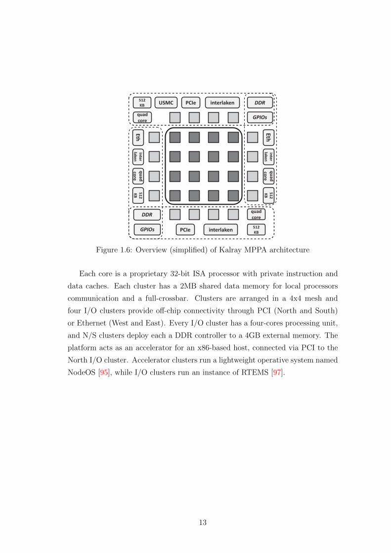
Kalray Multi Purpose Processor Array (MPPA) [72] is a family of low-power
many-core programmable processors for high-performance embedded systems.
The first product of the family, MPPA-256, deploys 256 general-purpose cores
grouped into 16 tightly-coupled clusters using a 28nm manufacturing process
technology.
The MPPA MANYCORE chip family scales from 256 to 1024 cores with a
performance of 500 Giga operations per second to more than 2 Tera operations per
second with typical 5W power consumption. Global communication among the
clusters is based on a Network-on-Chip. A simplified version of the architecture
is shown in Figure 1.6.
12
Eth
Inte
r
lake
n
qu
ad
core
51
2
KB
Eth
inte
r
lake
n
qu
ad
core
51
2
KB
PCIe interlaken
quad
core
512
KB
PCIe interlaken DDRUSMC
GPIOs
512
KB
quad
core
DDR
GPIOs
Figure 1.6: Overview (simplified) of Kalray MPPA architecture
Each core is a proprietary 32-bit ISA processor with private instruction and
data caches. Each cluster has a 2MB shared data memory for local processors
communication and a full-crossbar. Clusters are arranged in a 4x4 mesh and
four I/O clusters provide off-chip connectivity through PCI (North and South)
or Ethernet (West and East). Every I/O cluster has a four-cores processing unit,
and N/S clusters deploy each a DDR controller to a 4GB external memory. The
platform acts as an accelerator for an x86-based host, connected via PCI to the
North I/O cluster. Accelerator clusters run a lightweight operative system named
NodeOS [95], while I/O clusters run an instance of RTEMS [97].
13

14
Chapter 2
VirtualSoC: a Virtual Platform
for Design Space Exploration
2.1 Overview
Performance modeling plays a critical role in the design, evaluation, and develop-
ment of computing architecture of any segment, ranging from embedded to high
performance processors. Simulation has historically been the primary vehicle to
carry out performance modeling, since it allows for easily creating and testing new
designs several months before a physical prototype exists. Performance modeling
and analysis are now integral to the design flow of modern computing systems,
as it provides many significant advantages: i) accelerates time-to-market, by al-
lowing the development of software before the actual hardware exists; ii) reduces
development costs and risks, by allowing for testing new technology earlier in the
design process; iii) allows for exhaustive design space exploration, by evaluating
hundreds of simultaneous simulations in parallel.
High-end embedded processor vendors have definitely embraced the hetero-
geneous architecture template for their designs as it represents the most flexible
and efficient design paradigm in the embedded computing domain. Parallel ar-
chitecture and heterogeneity clearly provide a wider power/performance scaling,
combining high performance and power efficient general-purpose cores along with
15
massively parallel many-core-based accelerators. Examples and results of this
evolution are AMD Fusion [33], NVidia Tegra [96] and Qualcomm Snapdragon
[107]. Besides the complex hardware, generally these kinds of platforms host
also an advanced software eco-system, composed by an operating system, sev-
eral communication protocol stacks, and various computational demanding user
applications.
Unfortunately, as processor architectures get more heterogeneous and com-
plex, it becomes more and more difficult to develop simulators that are both
fast and accurate. Cycle-accurate simulation tools can reach an accuracy error
below 1-2%, but they typically run at a few millions of instructions per hour.
The necessity to efficiently cope with the huge HW/SW design space provided
by this target architecture makes clearly full-system simulator one of the most
important design tools. Clearly, the use of slow simulation techniques is challeng-
ing especially in the context of full-system simulation. In order to perform an
affordable processor design space exploration or software development for the tar-
get platform, trade-off accuracy for speed is thus necessary by implementing new
virtual platforms that allow for faster simulation speed at the expense of model-
ing fewer micro-architecture details of not-critical hardware components (like the
host processor domain), while keeping high-level of accuracy for the most critical
hardware components (like the manycore accelerator domain).
We present in this chapter VirtualSoC, a new virtual platform prototyping
framework targeting the full-system simulation of massively parallel heteroge-
neous system-on-chip composed by a general purpose processor (i.e. intended
as platform coordinator and in charge of running an operating system) and a
many-core hardware accelerator (i.e. used to speed-up the execution of com-
puting intensive applications or parts of them). VirtualSoC exploits the speed
and flexibility of QEMU, allowing the execution of a full-fledged Linux operating
system, and the accuracy of a SystemC model for many-core-based accelerators.
The specific features of VirtualSoC are:
� Since it exploits QEMU for the host processor emulation, unmodified op-
erating systems can be booted on VirtualSoC and the execution of unmod-
16
ified ARM binaries of applications and existing libraries can be simulated
on VirtualSoC.
� VirtualSoC enables accurate manycore-based accelerator simulation. We
designed a full software stack allowing the programmer to exploit the hard-
ware accelerator model implemented in SystemC, from within a user-space
application running on top of QEMU. This software stack comprise a Linux
device driver and a user-level programming API.
� The host processor (emulated by QEMU) and the SystemC accelerator
model can run in an asynchronous way, where a non-blocking communi-
cation interface has been implemented enabling parallel execution between
QEMU and SystemC environments.
� Beside the interface between QEMU and the SystemC model, we also im-
plemented a synchronization protocol able to provide a good approximation
of the global system time.
� VirtualSoC can be also used in stand-alone mode, where only the hardware
accelerator is simulated, thus enabling accurate design space explorations.
To the best of our knowledge, we are not aware of any existing public do-
main, open source simulator that rivals the characteristics of VirtualSoC. This
chapter focuses on the implementation details of VirtualSoC and evaluates the
performance of various benchmarks and presents some example case studies using
VirtualSoC.
The rest of the chapter is structured as follows: in Section 2.2 we provide
an overview of related work, in Section 2.3 we present the target architecture,
focusing on the many-core accelerator in Section 2.4. The implementation of
the proposed platform is discussed in Section 2.5. Software simulation support is
described in Section 2.6, finally experimental results and conclusions are presented
in Sections 2.7 and 2.8.
17
2.2 Related work
The importance of full-system emulation is confirmed by the considerable amount
of effort committed by both industry and research communities in developing such
designing tools as more efficient as possible. We can cite several examples, like
Bochs [77], Simics [84], Mambo [29], Parallel Embra [75], PTLsim [136], AMD
SimNow [24], OVPSim [126] and SocLib [87].
QEMU [25] is one of the most widely used open-source emulation platform.
QEMU supports cross-platform emulation and exploits binary translation for em-
ulating the target system. Taking advantage of the benefits of binary translation,
QEMU is very efficient and functionally correct, however it does not to pro-
vide any accurate information about hardware execution time. In [59] authors
have implemented program instrumentation capabilities to QEMU for user ap-
plication program analysis. This work has only been done for the user mode of
QEMU and it cannot be exploited for system performance measurements (e.g.
device driver). Moreover, profiling based on program instrumentation can heavily
change the execution flow of the program itself, leading to behaviors which will
never happen when executing the program in the native fashion. Authors in [89]
have instead presented pQEMU, which simulates the timing of instruction exe-
cutions and memory latencies. Instruction execution timings are simulated using
instruction classification and weight coefficients, while memory latency is simu-
lated using a set-associative cache and TLB simulator. This kind of approach can
lead to a significant overhead due to the different simulation stages (i.e. cache
simulation, TLB simulation), and even in this case the proposed framework can
only run user-level applications without the support of an operating system.
QEMU lacks also of any accurate co-processors simulation capabilities. Au-
thors in [109] interfaced QEMU with a many-core co-processor simulator running
on an nVidia GPGPU [103]. Despite the co-processor simulator described in [103]
is able to simulate thousands of computing units connected through a NoC, it
runs at a high level of abstraction and does not provide precise measurements
from the simulated architecture. Moreover authors do not address the problem
of timing synchronization between QEMU and the co-processor simulation.
18
Other works have been mainly concentrated on enabling either cycle accurate
instruction set simulators for the general purpose processor part or SystemC-
based simple peripherals, without considering complex many-core-based acceler-
ators [54].
When interfacing QEMU with the SystemC framework, several implementa-
tion aspects and decisions need to be accurately taken into account, since devel-
opment choices can limit and constraint the performance of the overall emulation
environment. The optimal implementation should not possibly affect efficiency,
flexibility and scalability.
Establishing the communication between QEMU and SystemC simulator
through inter-process communication socket is another approach. Authors in
[106] use such facility between a new component of QEMU, named QEMU-
SystemC Wrapper, and a modified version of the SystemC simulation kernel. The
exchanged messages have the purpose not only to transmit data and interrupt
signals but also to keep the simulation time synchronized between the simulation
kernels. However using heavy processes does not allow fast and efficient memory
sharing, which in this case can be achieved only using shared memory segments.
Moreover, Unix Domain Sockets are less efficient, in terms of performance and
flexibility, than direct communication between threads.
QEMU-SystemC [91] allows devices to be inserted into specific addresses of
QEMU and communicates by means of the PCI/AMBA bus interface. How-
ever, QEMU-SystemC does not provide the accurate synchronization information
that can be valuable to the hardware designers. [80] integrates QEMU with a
SystemC-based simulation development environment, to provide a system-level
development framework for high performance system accelerators. However, this
approach is based on socket communication, which strongly limits its perfor-
mance and flexibility. Authors in [135] suggested an approach based on threads
since context switches between threads are generally much faster than between
processes. However, communication among QEMU and SystemC uses a unidirec-
tional FIFO, limiting the interaction between QEMU and the SystemC model.
We present in this chapter a new emulation framework based on QEMU and
19
SystemC which overcomes these issues. We chose QEMU amongst all simulators
cited (e.g. OVPSim [126], Soclib [126]) because it is fast, open-source and also
very flexible enabling its extension with a moderate effort. Our approach is based
on thread parallelization and memory sharing to obtain a complete heterogeneous
SoC emulation platform. In our implementation the target processor and the Sys-
temC model can run in an asynchronous way, where non-blocking communication
is implemented through the use of shared memory between threads. Beside the
interface between QEMU and a SystemC model, we also present a lightweight
implementation of a synchronization protocol able to provide a good approxima-
tion of a global system time. Moreover, we designed a full SW stack allowing the
programmer to exploit the HW model implemented in SystemC, from within a
user-space application running on top of QEMU. This software stack comprise a
Linux device driver and a user-level programming API.
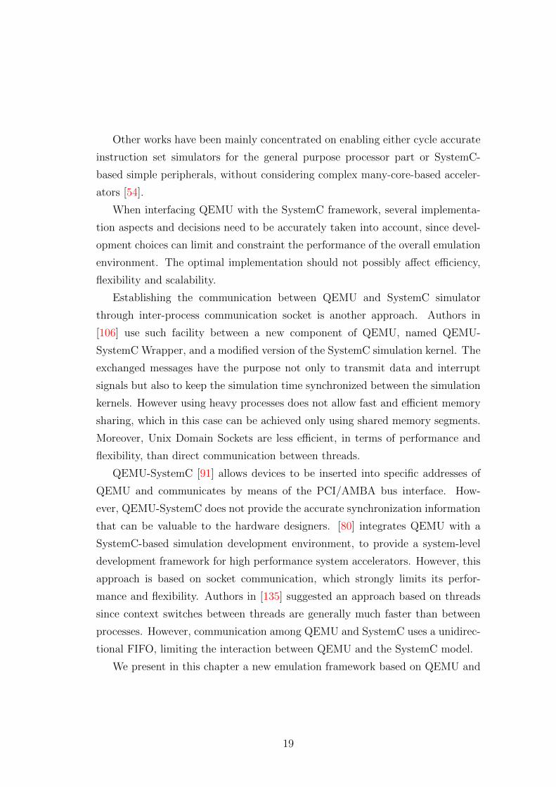
2.3 Target Architecture
Modern embedded SoCs are moving toward systems composed by a general pur-
pose multi-core processor accompanied by a more energy efficient and powerful
many-core accelerator (e.g. GPU). In these kinds of systems the general purpose
processor is intended as a coordinator and is in charge of running an operat-
ing system, while the many-core accelerator is used to speed up the execution of
computing intensive applications or parts of them. Despite their great computing
power, accelerators are not able to run an operating system due to the lack of
all needed surrounding devices and to the simplicity of their micro-architectural
design. The architecture targeted by this work (shown in Figure 6.1) is represen-
tative of the above mentioned platforms and composed by a many-core accelerator
and an ARM-based processor.
The ARM processor is emulated by QEMU which models an ARM926 proces-
sor, featuring an ARMv5 ISA, and interfaced with a group of peripherals needed
to run a full-fledged operating system (ARM Versatile Express baseboard). The
many-core accelerator is a SystemC cycle-accurate MPSoC simulator. The ARM
20
Co
re
I$
Co
re
I$
Co
re
I$
Co
re
I$
C
I$
C
I$
C
I$
C
I$
INTERCONNECTION
TCDMEXT
MEMMANY-CORE
ACCELERATOR
ARM
926
ARM processor !le
Daughter board
UARTs
RTC
MAIN MEMORY
HOST SUBSYSTEM
I/D $Display
Controller
Co
re
I$
Co
re
I$
Co
re
I$
Co
re
I$
C
I$
C
I$
C
I$
C
I$
Figure 2.1: Target simulated architecture
processor and the accelerator share the main memory, used as communication
medium between the two. The accelerator target architecture features a config-
urable number of simple RISC cores, with private or shared I-cache architecture,
all sharing a Tightly Coupled Data Memory (TCDM) accessible via a local inter-
connection. The state-of-the-art programming model for this kind of systems is
very similar to the one proposed by OpenCL [73]: a master application is running
on the host processor which, when encounters a data or task parallel section, of-
floads the computation to the accelerator. The master processor is in charge also
of transferring input and output data.
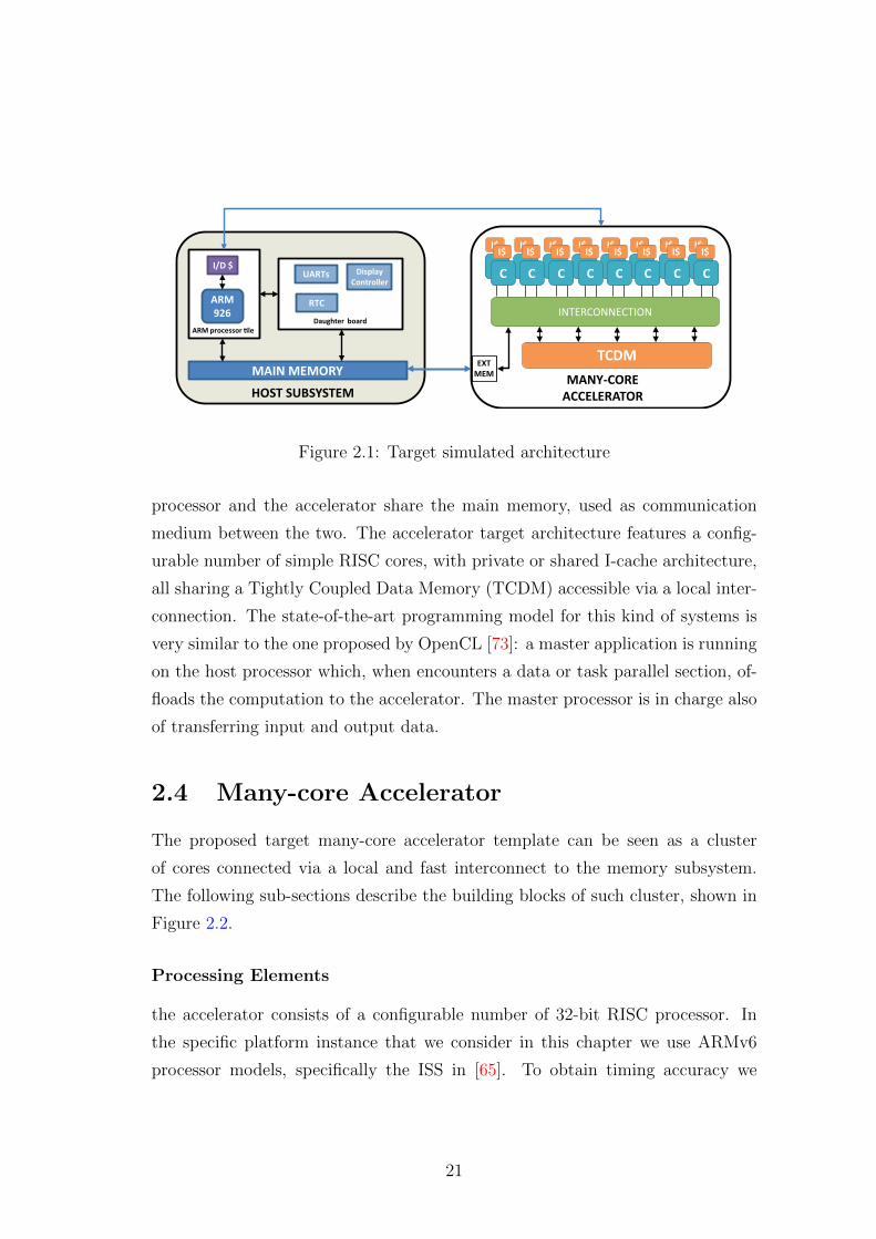
2.4 Many-core Accelerator
The proposed target many-core accelerator template can be seen as a cluster
of cores connected via a local and fast interconnect to the memory subsystem.
The following sub-sections describe the building blocks of such cluster, shown in
Figure 2.2.
Processing Elements
the accelerator consists of a configurable number of 32-bit RISC processor. In
the specific platform instance that we consider in this chapter we use ARMv6
processor models, specifically the ISS in [65]. To obtain timing accuracy we
21
CLUSTER INTERCONNECT (MoT)
L3INTERFACE
I$
PEN-1PE0 PE1 . . . . .
SHARED L1 TCDM
BANK M-1
SEM(TaS)
BANK 1
BANK 0
. . .
Figure 2.2: Many-core accelerator
modified its internal behavior to model a Harvard architecture and we wrapped
the ISS in a SystemC [7] module.
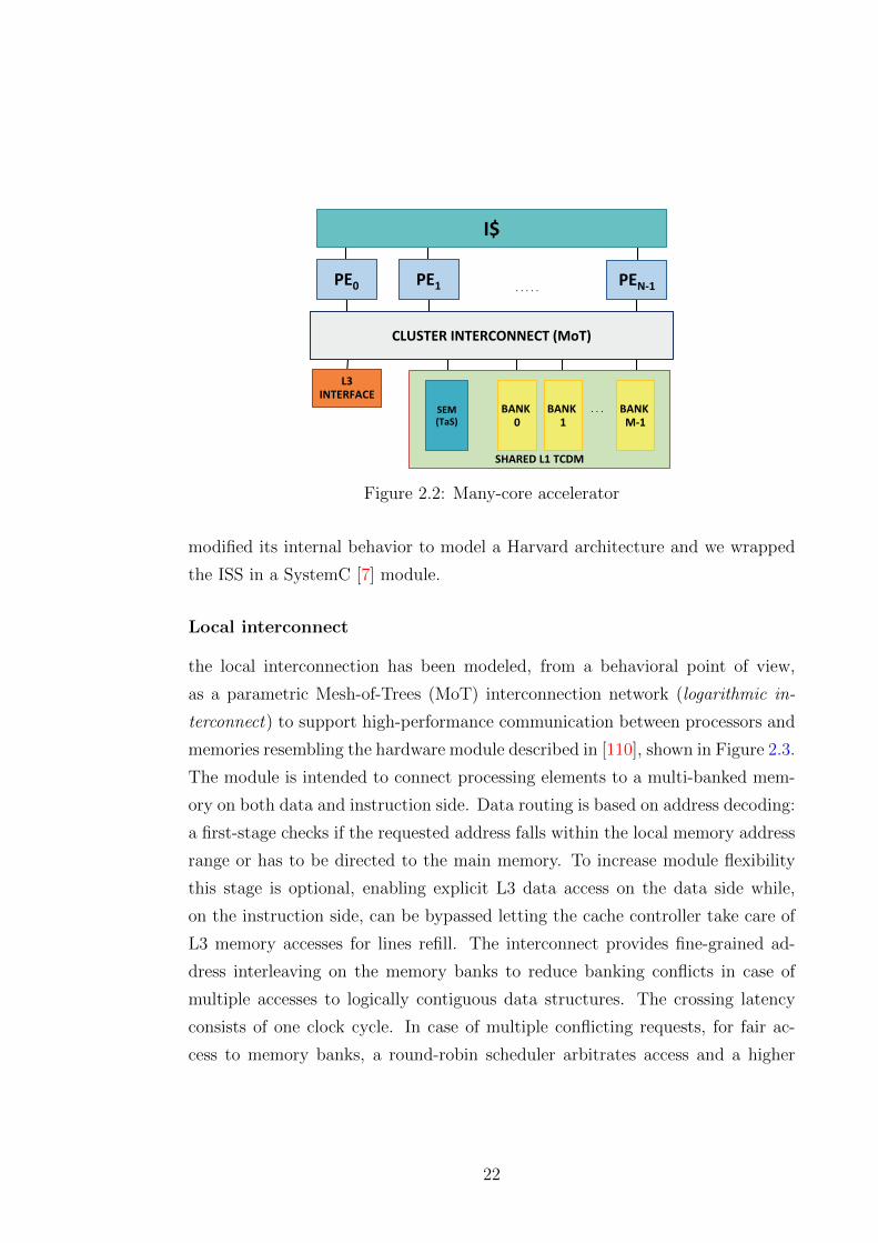
Local interconnect
the local interconnection has been modeled, from a behavioral point of view,
as a parametric Mesh-of-Trees (MoT) interconnection network (logarithmic in-
terconnect) to support high-performance communication between processors and
memories resembling the hardware module described in [110], shown in Figure 2.3.
The module is intended to connect processing elements to a multi-banked mem-
ory on both data and instruction side. Data routing is based on address decoding:
a first-stage checks if the requested address falls within the local memory address
range or has to be directed to the main memory. To increase module flexibility
this stage is optional, enabling explicit L3 data access on the data side while,
on the instruction side, can be bypassed letting the cache controller take care of
L3 memory accesses for lines refill. The interconnect provides fine-grained ad-
dress interleaving on the memory banks to reduce banking conflicts in case of
multiple accesses to logically contiguous data structures. The crossing latency
consists of one clock cycle. In case of multiple conflicting requests, for fair ac-
cess to memory banks, a round-robin scheduler arbitrates access and a higher
22
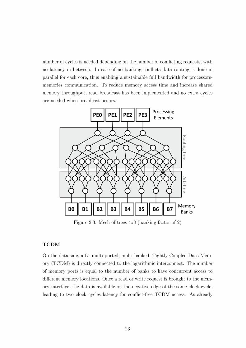
number of cycles is needed depending on the number of conflicting requests, with
no latency in between. In case of no banking conflicts data routing is done in
parallel for each core, thus enabling a sustainable full bandwidth for processors-
memories communication. To reduce memory access time and increase shared
memory throughput, read broadcast has been implemented and no extra cycles
are needed when broadcast occurs.
PE2PE1PE0
Rou�ngtre
eArb
tree
Processing
Elements
Memory
Banks
PE3
B7B6B5B4B3B2B1B0
Figure 2.3: Mesh of trees 4x8 (banking factor of 2)
TCDM
On the data side, a L1 multi-ported, multi-banked, Tightly Coupled Data Mem-
ory (TCDM) is directly connected to the logarithmic interconnect. The number
of memory ports is equal to the number of banks to have concurrent access to
different memory locations. Once a read or write request is brought to the mem-
ory interface, the data is available on the negative edge of the same clock cycle,
leading to two clock cycles latency for conflict-free TCDM access. As already
23
mentioned above, if conflicts occur there is no extra latency between pending
requests, once a given bank is active, it responds with no wait cycles.
Synchronization
To coordinate and synchronize cores execution the architecture exploits HW
semaphores mapped in a small subset of the TCDM address range. They consist
of a series of registers, accessible through the data logarithmic interconnect as a
generic slave, associating a single register to a shared data structure in TCDM.
By using a mechanism such as a hardware test&set, we are able to coordinate
access: if reading returns ’0’, the resource is free and the semaphore automati-
cally locks it, if it returns a different value, typically ’1’, access is not granted.
This module enables both single and two-phases synchronization barriers, easily
written at the software level.
Instruction Cache Architecture
the L1 Instruction Cache basic block has a core-side interface for instruction
fetches and an external memory interface for refill. The inner structure consists
of the actual memory and the cache controller logic managing the requests. The
module is configurable in its total size, associativity, line size and replacement
policy (FIFO, LRU, random). The basic block can be used to build different
Instruction Cache architectures:
� Private Instruction Cache: every processing element has its private I-cache,
each one with a separate cache line refill path to main memory leading to
high contention on external L3 memory.
� Shared Instruction Cache: there is no difference between the private ar-
chitecture in the data side except for the reduced contention L3 memory
(line refill path is unique in this architecture). Shared cache inner structure
is made of a configurable number of banks, a centralized logic to manage
requests and a slightly modified version of the logarithmic interconnect de-
scribed above: it connects processors to the shared memory banks operating
24
line interleaving (1 line consists of 4 words). A round robin scheduling guar-
antees fair access to the banks. In case of two or more processors requesting
the same instruction, they are served in broadcast not affecting hit latency.
In case of concurrent instruction miss from two or more banks, a simple bus
handles line refills in round robin towards the L3 bus.
2.5 Host-Accelerator Interface
In this section we describe the QEMU-based host side of VirtualSoC (VSoC-
Host), as well as the many-core accelerator side (VSoC-Acc).
Parallel Execution
In a real heterogeneous SoC host processor and accelerator can execute in an
asynchronous parallel fashion, and exchange data using non-blocking commu-
nication primitives. Usually the host processor, while running an application,
offloads asynchronously a parallel job to the accelerator and goes ahead with its
execution (Figure 2.4). Only when needed the host processor synchronizes with
the execution of the accelerator, to check the results of the computation.
In our virtual platform the host processor system and the accelerator can run
in parallel, with VSoC-Host and VSoC-Acc running on different threads: when
the thread of VSoC-Acc starts its execution triggers the SystemC simulation. It is
important to highlight that the VSoC-Acc SystemC simulation starts immediately
during VSoC-Host startup, and the accelerator starts executing the binary of a
firmware (until the shutdown) in which all cores are waiting for a job to execute.
Time Synchronization Mechanism
VSoC-Host and VSoC-Acc run independently in parallel with a different notion
of time. The lack of a common time measure leads to only functional simulation,
without the possibility of profiling applications performance even in a qualita-
tive way. Application developers often need to understand how much time, over
25
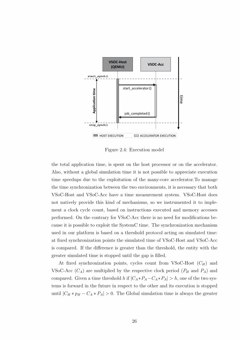
VSOC-Host
(QEMU)VSOC-Acc
time
start_accelerator ()
start_synch()
stop_synch()
job_completed ()Ap
pli
ca
on
m
e
HOST EXECUTION ACCELERATOR EXECUTION
Figure 2.4: Execution model
the total application time, is spent on the host processor or on the accelerator.
Also, without a global simulation time it is not possible to appreciate execution
time speedups due to the exploitation of the many-core accelerator.To manage
the time synchronization between the two environments, it is necessary that both
VSoC-Host and VSoC-Acc have a time measurement system. VSoC-Host does
not natively provide this kind of mechanisms, so we instrumented it to imple-
ment a clock cycle count, based on instructions executed and memory accesses
performed. On the contrary for VSoC-Acc there is no need for modifications be-
cause it is possible to exploit the SystemC time. The synchronization mechanism
used in our platform is based on a threshold protocol acting on simulated time:
at fixed synchronization points the simulated time of VSoC-Host and VSoC-Acc
is compared. If the difference is greater than the threshold, the entity with the
greater simulated time is stopped until the gap is filled.
At fixed synchronization points, cycles count from VSoC-Host (CH) and
VSoC-Acc (CA) are multiplied by the respective clock period (PH and PA) and
compared. Given a time threshold h if |CA∗PA−CA∗PA| > h, one of the two sys-
tems is forward in the future in respect to the other and its execution is stopped
until |CH ∗ pH − CA ∗ PA| > 0. The Global simulation time is always the greater
26
of the two. It is intuitive to note that the proposed mechanism slows down the
simulation speed, due to synchronization points and depending on the difference
of simulation speed between the two ecosystems. To avoid unnecessary slowdown,
we provide an interface to activate and de-activate the time synchronization when
it is not needed (e.g. functional simulation).
2.6 Simulation Software Support
In this section we provide a description of the software stack provided with the
simulator to allow the programmer to fully exploit the accelerator from within
the host Linux system, and to write parallel code to be accelerated.
Linux Driver
In order to build a full system simulation environment we mapped VSoC-Acc
as a device in the device file system of the guest Linux environment running on
top of VSoC-Host. A device node /dev/vsoc has been created, and as all Linux
devices it is interfaced to the operating system using a Linux driver. The driver
is in charge of mapping the shared memory region into the kernel I/O space.
This region is not managed under virtual memory because the accelerator can
deal only with physical addresses, as a consequence all buffers must be allocated
contiguously (done by the Linux driver). The driver provides all basic functions
to interact with the device.
Host Side User-Space Library
To simplify the job of the programmer we have designed a user level library,
which provides a set of APIs that rely on the Linux driver functions. Through
this library the programmer is able to fully control the accelerator from the host
Linux system. It is possible for example to offload a binary, or to check the status
of the current executing job (e.g. checking if it has finished).
27
Accelerator Side Software Support
The basic manner we provide to write applications for the accelerator is to di-
rectly call from the program a set of low-level functions implemented as a user
library, called appsupport. appsupport provides basic services for memory man-
agement, core ID resolution, synchronization. To further simplify programming
and raise the level of abstraction we also support a fully-compliant OpenMP v3.0
programming model, with associated compiler and runtime library.
2.7 Evaluation
In this section two use cases of the simulation platform are presented. We will
show how the proposed virtual platform can be exploited for both software veri-
fication or design space exploration.
2.7.1 Experimental Setup
Table 2.1 summarizes the experimental setup of the virtual platform used for all
benchmarks discussed. We chose as ARM core clock frequency of 1GHz, even
if the ARM modeled by QEMU works at up to 500MHz, to resemble a state of
the art ARM processor performance. The frequency would only affect results in
terms of global values, all considerations done in this section remain valid even if
the ARM core clock frequency is changed.
2.7.2 VirtualSoC Use Cases
Full System Simulation
As first use case of the simulator we propose the profiling of an application involv-
ing both the ARM host and the many-core accelerator. In this example we want
to measure the speedup achievable when accelerating a set of algorithms onto the
many-core accelerator. The algorithms chosen are: Matrix Multiplication, RG-
BtoHPG color conversion, and Image Rotation algorithm. All the benchmarks
28
follow a common scheme: the computation starts from the ARM host which in
turn will offload a parallel task, one of the algorithms, to the accelerator. Then
we compare simulated time obtained varying the number of cores present in the
accelerator, with the time taken to run each benchmark on the ARM processor
only (i.e. no acceleration).
Figure 2.5 shows the results of this experiment. Using the accelerator with 8
cores we can see a speedup of ≈ 3× times for the matrix multiplication, ≈ 3× for
the rotate benchmark and ≈ 5× for the RGBtoHPG benchmark. When running
with 16 cores we can appreciate an almost double execution speedup for all the
proposed benchmarks.
Standlone Accelerator Simulation
In this section we show an example of stand-alone accelerator analysis by us-
ing two real applications, namely a JPEG decoder and a Scale Invariant Feature
Transform (SIFT), a widely adopted algorithm in the domain of image recogni-
tion. Our analysis will as first evaluate the effects of L3 latency over the execution
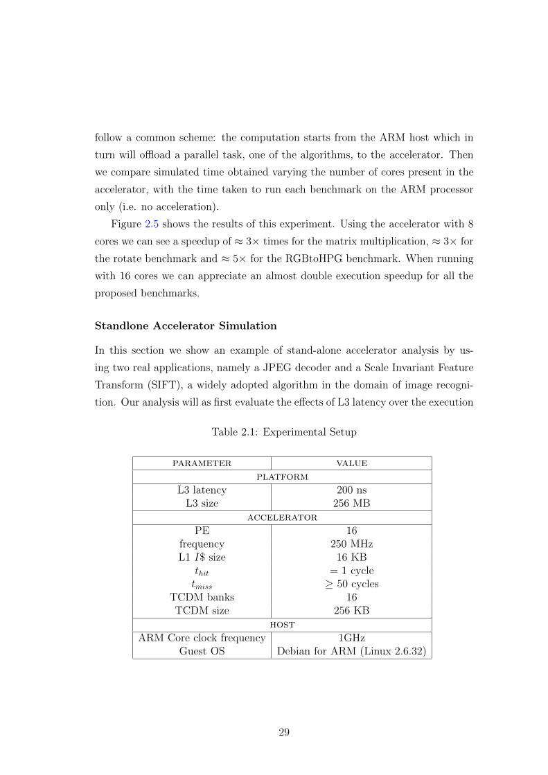
Table 2.1: Experimental Setup
parameter valueplatform
L3 latency 200 nsL3 size 256 MB
acceleratorPE 16
frequency 250 MHzL1 I$ size 16 KB
thit = 1 cycletmiss ≥ 50 cycles
TCDM banks 16TCDM size 256 KB
hostARM Core clock frequency 1GHz
Guest OS Debian for ARM (Linux 2.6.32)
29
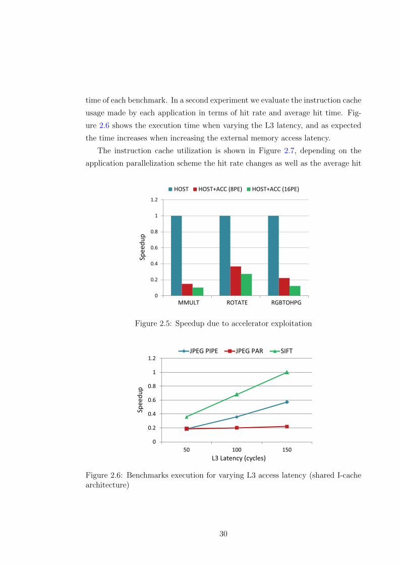
time of each benchmark. In a second experiment we evaluate the instruction cache
usage made by each application in terms of hit rate and average hit time. Fig-
ure 2.6 shows the execution time when varying the L3 latency, and as expected
the time increases when increasing the external memory access latency.
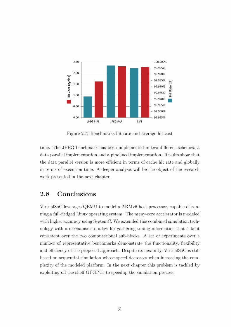
The instruction cache utilization is shown in Figure 2.7, depending on the
application parallelization scheme the hit rate changes as well as the average hit
0
0.2
0.4
0.6
0.8
1
1.2
MMULT ROTATE RGBTOHPG
Sp
ee
du
p
HOST HOST+ACC (8PE) HOST+ACC (16PE)
Figure 2.5: Speedup due to accelerator exploitation
0
0.2
0.4
0.6
0.8
1
1.2
50 100 150
Sp
ee
du
p
L3 Latency (cycles)
JPEG PIPE JPEG PAR SIFT
Figure 2.6: Benchmarks execution for varying L3 access latency (shared I-cachearchitecture)
30
99.955%
99.960%
99.965%
99.970%
99.975%
99.980%
99.985%
99.990%
99.995%
100.000%
0.00
0.50
1.00
1.50
2.00
2.50
JPEG PIPE JPEG PAR SIFT
Hit
Ra
te (
%)
Hit
Co
st (
cycl
es)
Figure 2.7: Benchmarks hit rate and average hit cost
time. The JPEG benchmark has been implemented in two different schemes: a
data parallel implementation and a pipelined implementation. Results show that
the data parallel version is more efficient in terms of cache hit rate and globally
in terms of execution time. A deeper analysis will be the object of the research
work presented in the next chapter.
2.8 Conclusions
VirtualSoC leverages QEMU to model a ARMv6 host processor, capable of run-
ning a full-fledged Linux operating system. The many-core accelerator is modeled
with higher accuracy using SystemC. We extended this combined simulation tech-
nology with a mechanism to allow for gathering timing information that is kept
consistent over the two computational sub-blocks. A set of experiments over a
number of representative benchmarks demonstrate the functionality, flexibility
and efficiency of the proposed approach. Despite its flexibilty, VirtualSoC is still
based on sequential simulation whose speed decreases when increasing the com-
plexity of the modeled platform. In the next chapter this problem is tackled by
exploiting off-the-shelf GPGPUs to speedup the simulation process.
31

32
Chapter 3
GP-GPU based Acceleration of
Virtual Platforms
3.1 Overview
Simulation is one of the primary techniques for application development in the
high performance computing (HPC) domain. Virtual platforms and simulators
are key tools both for the early exploration of new processor architectures and
for advanced software development for upcoming machines. They are indeed
extensively used for early software development (i.e. before the real hardware is
available), and to optimize the hardware resources utilization of the application
itself when the real hardware is already there. With simulators, the performance
debugging cycle can be shortened considerably. However, simulation times are
increasing further by the needs to simulate a still wider range of inputs, larger
datasets, but, even more importantly, processors with an increasing number of
cores.
During last decade the design of integrated architectures has indeed been char-
acterized by a paradigm shift: boosting clock frequencies of monolithic processor
cores has clearly reached its limits [67], and designers are turning to multicore
architectures to satisfy the growing computational needs of applications within
a reasonable power envelope [30]. This ever-increasing complexity of computing
33
systems is dramatically changing their system design, analysis and programming
[48].
New trends in chip design and the ever increasing amount of logic that can be
placed onto a single silicon die are affecting the way of developing the software
which will run on future parallel computing platforms. Hardware designers will
be soon capable to create integrated circuits with thousands of cores and a huge
amount of on-chip fast memory [99]. This evolution of the hardware architectural
concept will bring to a revolution of the idea of how thinking and structuring the
software for parallel computing systems [16]. The existing relation between com-
putation and communication will deeply change: past and current architectures
are equipped with few processors and small on-chip memory, which can interact
via off-chip buses. Future architectures will expose a massive battery of paral-
lel processors and large on-chip memories connected through a network-on-chip,
which speed is more than hundred times faster than the off-chip one [39]. It is
clear that current virtual platform technologies are not able to tackle the possible
issues coming by the complexity derived by simulating this future scenario, be-
cause they suffer problems of either performance or accuracy. Cycle- and signal-
accurate simulators are extensively used for architectural explorations, but they
are not adequate for simulating large systems as they are sequential and slow.
On the contrary, high level and hardware-abstracting simulation technologies can
provide good performance for software development, but can not enable reliable
design space explorations or system performance metrics because they are lack-
ing low level architectural details. For example, they are not capable of modeling
contention on memory hierarchy, system buses or network. Parallel simulators
have been also proposed to address the problems of simulation duration and
complexity [138][23], but they require multiple processing nodes to increase the
simulation rate and suffer poor scalability due to the synchronization overhead
when increasing the number of processing nodes.
None of the current simulators takes advantage of the computational power
provided by modern manycores, like General Purpose Graphic Processing Units
(GPGPU) [4]. The development of computer technology brought to an unprece-
34
dent performance increase with these new architectures. They provide both scal-
able computation power and flexibility, and they have already been adopted for
many computation-intensive applications [5]. However, in order to obtain the
highest performance on such a machine, the programmer has to write programs
that best exploit the hardware architecture.
The main novelty of this chapter is the development of fast and parallel simu-
lation technology targeting extremely parallel embedded systems (i.e. composed
of thousands of cores) by specifically taking advantage of the inherent parallel
processing power available in modern GPGPUs. The simulation of manycore
architectures indeed exhibits a high level of parallelism and is thus inherently
parallelizable. The large number of threads that can be executed in parallel on
a GPGPU can be employed to simulate as many target processors in parallel.
Research projects such as Eurocloud[2] are building platforms to support thou-
sands of ARM cores in a single server. To provide the simulation infrastructure
for such large many core system we are developing a new technology to deploy
parallel full system simulation on top of GPGPUs. The simulated architecture
is composed by several cores (i.e. ARM ISA based), with instruction and data
caches, connected through a Network-on-Chip (NoC). Our GPU-based simulator
is not intended to be cycle-accurate, but instruction accurate. Its simulation en-
gine and models provide accurate estimates of performance and various statistics.
Our experiments confirm the feasibility and goodness of our idea and approach,
as our simulator can model architectures composed of thousands of cores while
providing fast simulation time and good scalability.
3.2 Related Work
In this section we give an overview about the state of the art in the context of
architectural simulation of large computing systems. A considerable number of
simulators has been developed by both scientific and industrial communities. We
will try to present and extensively review the simulation environments that are
most representative and widely used in the scientific community. We also high-
35
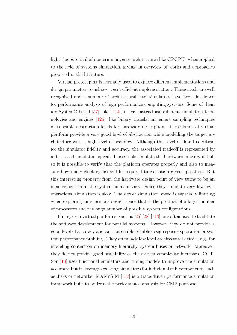
light the potential of modern manycore architectures like GPGPUs when applied
to the field of systems simulation, giving an overview of works and approaches
proposed in the literature.
Virtual prototyping is normally used to explore different implementations and
design parameters to achieve a cost efficient implementation. These needs are well
recognized and a number of architectural level simulators have been developed
for performance analysis of high performance computing systems. Some of them
are SystemC based [57], like [114], others instead use different simulation tech-
nologies and engines [126], like binary translation, smart sampling techniques
or tuneable abstraction levels for hardware description. These kinds of virtual
platform provide a very good level of abstraction while modelling the target ar-
chitecture with a high level of accuracy. Although this level of detail is critical
for the simulator fidelity and accuracy, the associated tradeoff is represented by
a decreased simulation speed. These tools simulate the hardware in every detail,
so it is possible to verify that the platform operates properly and also to mea-
sure how many clock cycles will be required to execute a given operation. But
this interesting property from the hardware design point of view turns to be an
inconvenient from the system point of view. Since they simulate very low level
operations, simulation is slow. The slower simulation speed is especially limiting
when exploring an enormous design space that is the product of a large number
of processors and the huge number of possible system configurations.
Full-system virtual platforms, such as [25] [28] [113], are often used to facilitate
the software development for parallel systems. However, they do not provide a
good level of accuracy and can not enable reliable design space exploration or sys-
tem performance profiling. They often lack low level architectural details, e.g. for
modeling contention on memory hierarchy, system buses or network. Moreover,
they do not provide good scalability as the system complexity increases. COT-
Son [13] uses functional emulators and timing models to improve the simulation
accuracy, but it leverages existing simulators for individual sub-components, such
as disks or networks. MANYSIM [137] is a trace-driven performance simulation
framework built to address the performance analysis for CMP platforms.
36
Also companies showed interest in such field: Simics [84] and AMD SimNow
[24] are just few representative examples. However, commercial virtual platforms
often suffer from the limitations of not being open source products, and they also
provide poor scalability when dealing with increasing complexity in the simulated
architecture.
Complex models generally require significant execution times and may be
beyond the capability of a sequential computer. Full-system simulators have
been also implemented on parallel computers with significant compute power and
memory capacity [112] [49]. In the parallel simulation, each simulated processor
works on its own by selecting the earliest event available to it and processing it
without knowing what happens on other simulated processors [105][138]. Thus,
methods for synchronizing the execution of events across simulated processors are
necessary for assuring the correctness of the simulation [46] [119] [118]. Parallel
simulators [138][23] require multiple processing nodes to increase the simulation
rate and suffer of poor scalability due to the synchronization overhead when
increasing the number of processing nodes.
From this brief overview in the literature of system simulation, it can be no-
ticed that achieving high performance with reasonable accuracy is a challenging
task, even if the simulation of large-scale systems exposes a high level of paral-
lelism. Moreover, none of the aforementioned simulation environments exploits
the powerful computational capabilities of modern GPGPUs. In the last decade,
GPU performance has been increasing very fast. Besides performance improve-
ment of the hardware, the programmability also has been significantly increased.
In the past, hardware special-purpose machines have been proposed for many-
core system emulation and to assist in the application development process for
multi-core processors [122][38]. Even if these solutions provide good performance,
a software GPGPU-based solution provides better flexibility and scalability, more-
over it is cheaper and more accessible to a wider community. Recently, a few
research solutions have been proposed to run gate-level simulations on GPUs
[35]. A first attempt by authors in [86] did not provide performance benefits
due to lack of general purpose programming primitives for their platform and
37
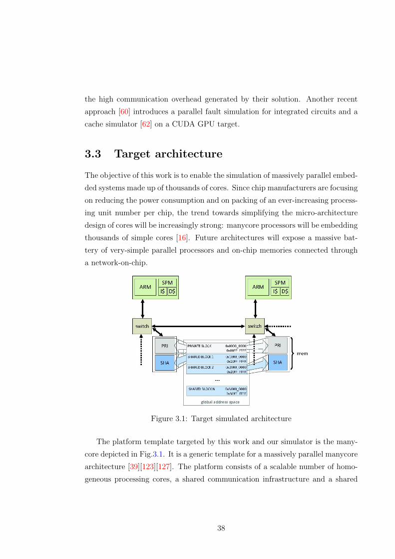
the high communication overhead generated by their solution. Another recent
approach [60] introduces a parallel fault simulation for integrated circuits and a
cache simulator [62] on a CUDA GPU target.
3.3 Target architecture
The objective of this work is to enable the simulation of massively parallel embed-
ded systems made up of thousands of cores. Since chip manufacturers are focusing
on reducing the power consumption and on packing of an ever-increasing process-
ing unit number per chip, the trend towards simplifying the micro-architecture
design of cores will be increasingly strong: manycore processors will be embedding
thousands of simple cores [16]. Future architectures will expose a massive bat-
tery of very-simple parallel processors and on-chip memories connected through
a network-on-chip.
Figure 3.1: Target simulated architecture
The platform template targeted by this work and our simulator is the many-
core depicted in Fig.3.1. It is a generic template for a massively parallel manycore
architecture [39][123][127]. The platform consists of a scalable number of homo-
geneous processing cores, a shared communication infrastructure and a shared
38
memory for inter-tile communication. The main architecture is made by several
computational tiles composed by a ARM-based CPU. Processing cores embed in-
struction and data caches and are directly connected to tightly coupled software
controlled scratch-pad memories.
Each computational tile also features a bank of private memory, only acces-
sible by the local processor, and a bank of shared memory. The collection of all
the shared segments is organized as a globally addressable NUMA portion of the
address space.
Interaction between CPUs and memories takes place through a Network-on-
Chip communication network (NoC).
3.4 The Fermi GPU Architecture and CUDA
The Fermi-based GPU used in this work is a Nvidia GeForce GTX 480, a two-
level shared memory parallel machine comprising 480 SPs organized in 16 SMs
(Streaming Multiprocessors). Streaming multiprocessors manage the execution
of programs using so called “warps”, groups of 32 threads. Each SM features
two warp schedulers and two instruction dispatch units, allowing two warps to
be issued and executed concurrently. All instructions are executed in a SIMD
fashion, where one instruction is applied to all threads in warp. This execution
method is called SIMT (Single Instruction Multiple Threads). All threads in a
warp execute the same instruction or remain idle (different threads can perform
branching and other forms of independent work). Warps are scheduled by special
units in SMs in such a way that, without any overhead, several warps execute
concurrently by interleaving their instructions. One of the key architectural in-
novations that greatly improved both the programmability and performance of
GPU applications is on-chip shared memory. In the Fermi architecture, each SM
has 64 KB of on-chip memory that can be configured as 48 KB of shared mem-
ory with 16 KB of L1 cache or as 16 KB of shared memory with 48 KB of L1
cache. Fermi features also a 768 KB unified L2 cache which provides efficient
data sharing across the GPU.
39
CUDA (Compute Unified Device Architecture) is the software architecture for
issuing and managing computations on the GPU. CUDA programming involves
running code on two different platforms: a host system that relies on one or more
CPUs to perform calculations, and a CUDA-enabled NVIDIA GPU (the device).
The device works as a coprocessor to the host, so a part of the application is
executed on the host and the rest, typically calculation intensive, on the device.
3.4.1 Key Implementative Issues for Performance
When writing applications it is important to take into account the organization
of the work, i.e. to use 32 threads simultaneously. The code that does not
break into 32 thread units can have lower performance. Hardware chooses which
warp to execute at each cycle, and it switches between them without penalties.
Compared with CPUs, it is similar to simultaneously executing 32 programs and
switching between them at each cycle without penalties. CPU cores can actually
execute only one program at a time, and switching to other programs has a cost
of hundreds of cycles.
Another key aspect to achieving performance in CUDA application is an effi-
cient management of accesses to the global memory. These are performed without
an intervening caching mechanism, and thus are subject to high latencies.
To maximally exploit the memory bandwidth is necessary to leverage some
GPU peculiarities:
� All active threads in a half-warp execute the same instruction;
� Global memory is seen as a set of 32, 64 or 128 byte segments. This implies
that a single memory transaction involves at least a 32 byte transfer.
By properly allocating data to memory, accesses from a halfwarp are trans-
lated into a single memory transaction (access coalescing). More specifically, if
all threads in a half-warp are accessing 32-bit data in global memory it is possible
to satisfy the entire team’s requests with a single 64-Byte (32 bit x 16 threads)
transfer.All the above mentioned aspects were taken into account to optimize the
performance of code running on GPGPUs.
40
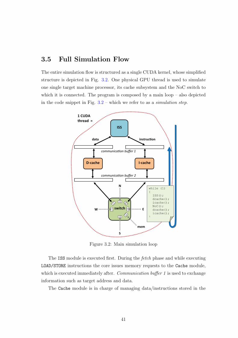
3.5 Full Simulation Flow
The entire simulation flow is structured as a single CUDA kernel, whose simplified
structure is depicted in Fig. 3.2. One physical GPU thread is used to simulate
one single target machine processor, its cache subsystem and the NoC switch to
which it is connected. The program is composed by a main loop – also depicted
in the code snippet in Fig. 3.2 – which we refer to as a simulation step.
ISS
D-cache I-cache
switch
data instruc!on
communica on buffer 1
communica on buffer 2
E
N
S
W
mem
1 CUDA
thread =
while (1)
{
ISS();
dcache();
icache();
NoC();
dcache();
icache();
}
Figure 3.2: Main simulation loop
The ISS module is executed first. During the fetch phase and while executing
LOAD/STORE instructions the core issues memory requests to the Cache module,
which is executed immediately after. Communication buffer 1 is used to exchange
information such as target address and data.
The Cache module is in charge of managing data/instructions stored in the
41
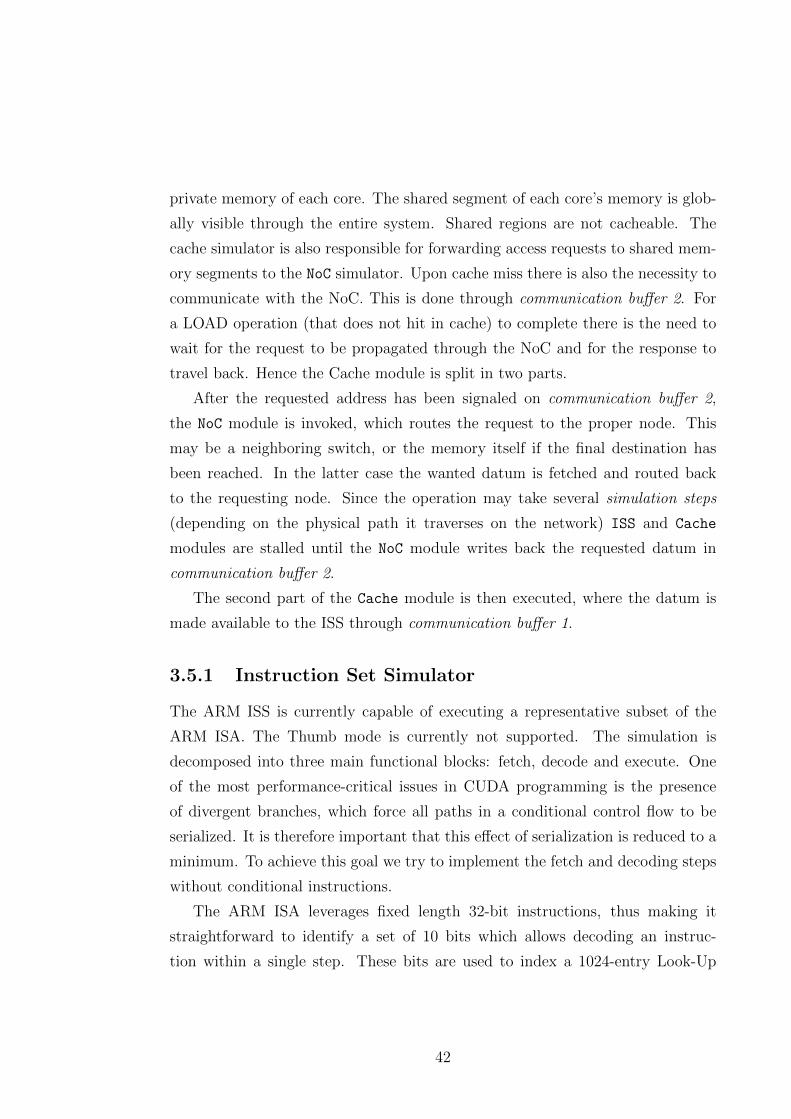
private memory of each core. The shared segment of each core’s memory is glob-
ally visible through the entire system. Shared regions are not cacheable. The
cache simulator is also responsible for forwarding access requests to shared mem-
ory segments to the NoC simulator. Upon cache miss there is also the necessity to
communicate with the NoC. This is done through communication buffer 2. For
a LOAD operation (that does not hit in cache) to complete there is the need to
wait for the request to be propagated through the NoC and for the response to
travel back. Hence the Cache module is split in two parts.
After the requested address has been signaled on communication buffer 2,
the NoC module is invoked, which routes the request to the proper node. This
may be a neighboring switch, or the memory itself if the final destination has
been reached. In the latter case the wanted datum is fetched and routed back
to the requesting node. Since the operation may take several simulation steps
(depending on the physical path it traverses on the network) ISS and Cache
modules are stalled until the NoC module writes back the requested datum in
communication buffer 2.
The second part of the Cache module is then executed, where the datum is
made available to the ISS through communication buffer 1.
3.5.1 Instruction Set Simulator
The ARM ISS is currently capable of executing a representative subset of the
ARM ISA. The Thumb mode is currently not supported. The simulation is
decomposed into three main functional blocks: fetch, decode and execute. One
of the most performance-critical issues in CUDA programming is the presence
of divergent branches, which force all paths in a conditional control flow to be
serialized. It is therefore important that this effect of serialization is reduced to a
minimum. To achieve this goal we try to implement the fetch and decoding steps
without conditional instructions.
The ARM ISA leverages fixed length 32-bit instructions, thus making it
straightforward to identify a set of 10 bits which allows decoding an instruc-
tion within a single step. These bits are used to index a 1024-entry Look-Up
42
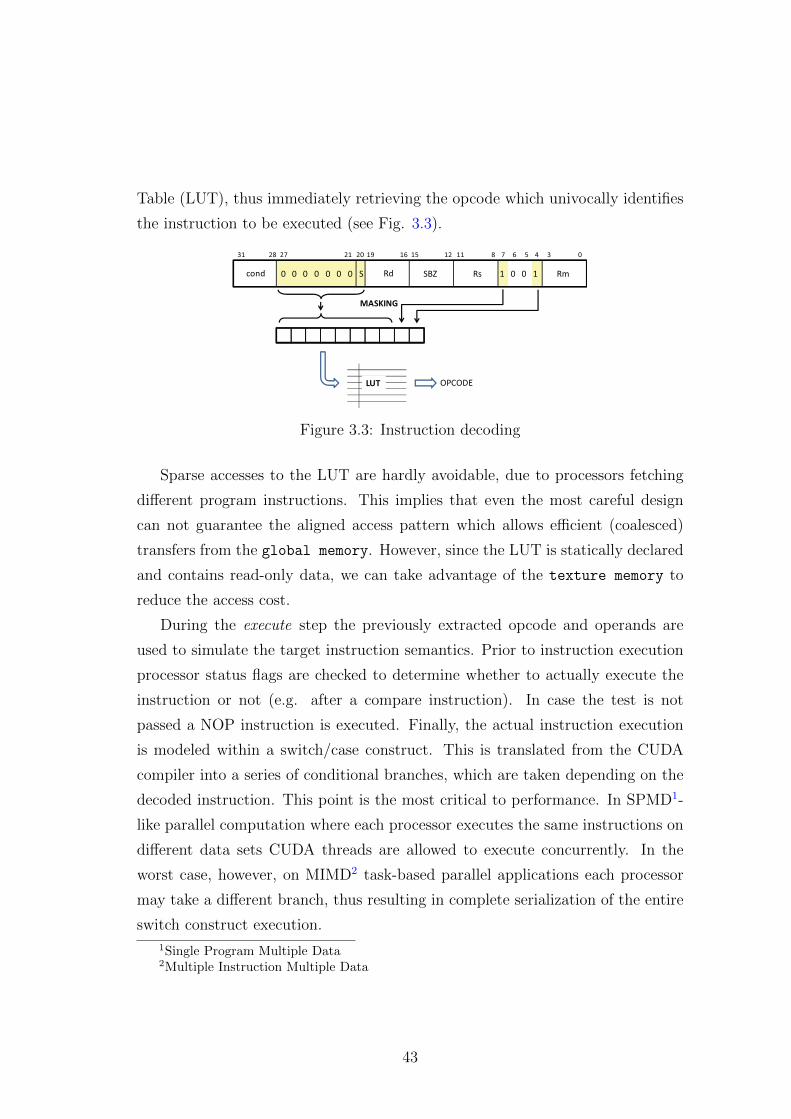
Table (LUT), thus immediately retrieving the opcode which univocally identifies
the instruction to be executed (see Fig. 3.3).
MASKING
OPCODE
cond 0 0 0 0 0 0 0 S Rd SBZ Rs Rm1 0 0 1
31 28 27 21 20 19 16 15 12 11 8 7 6 5 4 3 0
LUT
Figure 3.3: Instruction decoding
Sparse accesses to the LUT are hardly avoidable, due to processors fetching
different program instructions. This implies that even the most careful design
can not guarantee the aligned access pattern which allows efficient (coalesced)
transfers from the global memory. However, since the LUT is statically declared
and contains read-only data, we can take advantage of the texture memory to
reduce the access cost.
During the execute step the previously extracted opcode and operands are
used to simulate the target instruction semantics. Prior to instruction execution
processor status flags are checked to determine whether to actually execute the
instruction or not (e.g. after a compare instruction). In case the test is not
passed a NOP instruction is executed. Finally, the actual instruction execution
is modeled within a switch/case construct. This is translated from the CUDA
compiler into a series of conditional branches, which are taken depending on the
decoded instruction. This point is the most critical to performance. In SPMD1-
like parallel computation where each processor executes the same instructions on
different data sets CUDA threads are allowed to execute concurrently. In the
worst case, however, on MIMD2 task-based parallel applications each processor
may take a different branch, thus resulting in complete serialization of the entire
switch construct execution.
1Single Program Multiple Data2Multiple Instruction Multiple Data
43
The execution contexts of simulated cores are represented with 16 general-
purpose registers, a status register plus an auxiliary register used for exception
handling, or to signal the end of execution. Due to the frequent accesses per-
formed by every program to its execution context, the data structure was placed
in the low latency shared memory rather than accessing it from much slower
global memory.
3.5.2 Cache Simulator
The main architectural features of the simulated cache are summarized in Table
3.1. Our implementation is based on a set-associative design, which is fully re-
configurable in terms of number of ways thus also allowing the exploration of
fully-associative and direct-mapped devices. The size of the whole cache and of a
single line is also parameterized.
Type set-associative (default 8 ways)Write policy write backAllocation write allocate, write no allocateReplacement policy FIFOData format word, half word, byte
Table 3.1: Cache design parameters
Currently we only allow a common setup for cache parameters (i.e. we simu-
late identical devices). No coherence protocols or commands (i.e. explicit inval-
idation, flush) are available at the moment. We prevent data consistency issues
by designing the memory subsystem as follows:
1. Caches are private to each core, meaning that they only deal with data/in-
structions allocated in the private memory. This implies that cache lines
need not be invalidated upon memory updates performed by other proces-
sors.
2. Shared memory regions are directly accessible from every processor, and
the corresponding address range is disregarded by the caching policy.
44
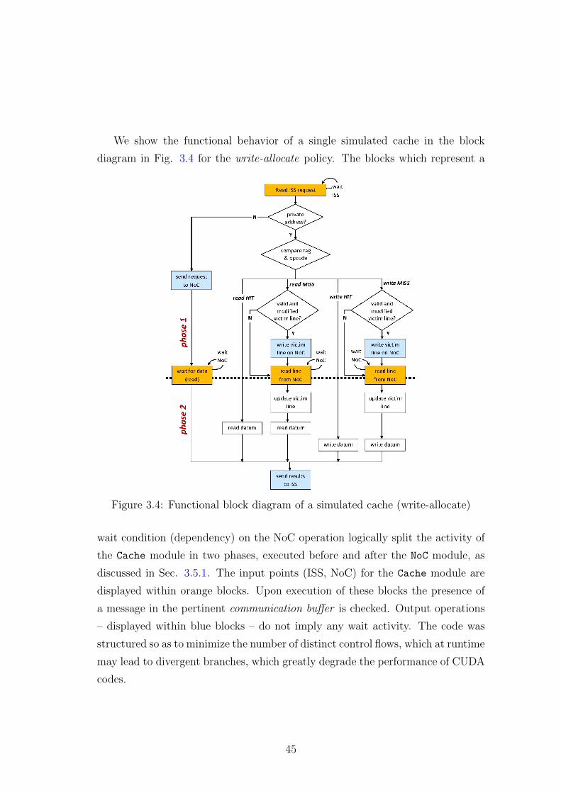
We show the functional behavior of a single simulated cache in the block
diagram in Fig. 3.4 for the write-allocate policy. The blocks which represent a
Figure 3.4: Functional block diagram of a simulated cache (write-allocate)
wait condition (dependency) on the NoC operation logically split the activity of
the Cache module in two phases, executed before and after the NoC module, as
discussed in Sec. 3.5.1. The input points (ISS, NoC) for the Cache module are
displayed within orange blocks. Upon execution of these blocks the presence of
a message in the pertinent communication buffer is checked. Output operations
– displayed within blue blocks – do not imply any wait activity. The code was
structured so as to minimize the number of distinct control flows, which at runtime
may lead to divergent branches, which greatly degrade the performance of CUDA
codes.
45
3.5.2.1 Communication buffers
Communication between the Cache module and the ISS and NoC modules takes
place through shared memory regions acting as shared buffers. Information ex-
change exploits the producer/consumer paradigm, but without the need for syn-
chronization since ISS, cache and NoC modules are executed sequentially.
Buffers amidst ISS and Cache modules (communication buffer 1 ) host mes-
sages structured as follows:
1. a single-bit flag (full) indicating that a valid message is present in the
buffer
2. an opcode which specifies the operation type (LOAD, STORE) and the size
of the datum (word, byte)
3. a 32-bit address field
4. a 32-bit data field
The full and opcode fields are duplicated to properly handle bi-directional mes-
sages (i.e. traveling from/to the ISS). The address field is only meaningful for
ISS-to-Cache communication, whereas the data field is exploited on both direc-
tions. In case of a STORE operation it carries the datum to be written in memory.
In case of a LOAD operation it is used only when the cache responds to the ISS.
Messages exchanged between Cache and NoC modules (stored in communica-
tion buffer 2 ) have a slightly different structure. First, the data field must ac-
commodate an entire cache line in case of a burst read/write to private addresses.
If the requested address belongs to the shared range a single-word read/write op-
eration is issued, and only 32 bits of the data field are used. Second, the opcode
field should still discriminate between LOAD/STORE operations and data sizes.
The latter have however a different meaning. For a cache miss (private reference)
the only allowed type is a cache line. For shared references it is still necessary
to distinguish between word, half-word and byte types. Third, in case of a cache
miss which also requires the eviction of a (valid and modified) line it is also nec-
46
essary to instruct the NoC about the replacement of the victim line. To handle
this particular situation we add the following fields to the communication buffer:
1. a single-bit evict field, which notifies the NoC about the necessity for line
replacement
2. an additional address field which holds the pointer to the destination of
the evicted cache line
The data field can be exploited to host both the evicted line and the substitute.
3.5.3 Network-on-Chip Simulator
The central element of the NoC simulation is a switch. Each switch in the network
for the considered target architecture (cfr. Sec. 3.3) is physically connected to (up
to) four neighbors, the local memory bank (private + shared) and the instruction
and data caches. We thus consider each switch as having seven ports, modeled
with as many packet queues. For each switch the simulation loop continuously
executes the following tasks:
1. check the input queues for available packets
2. in case the packet is addressed to the local node, insert packet in the memory
queue
3. otherwise, route the packet to the next hop of the path
Packet queues are stored in global memory. Hosting them on the local (shared)
memory would have allowed faster access time, but is subject to several practical
limitations. First, local memory is only shared among threads hosted on the
same multiprocessor, thus complicating communication between notes simulated
by threads residing on different devices (multiprocessors). Second, the shared
memory has a limited size, which in turn limits the maximum number of switches
that could be simulated (i.e. the size of the system).
47
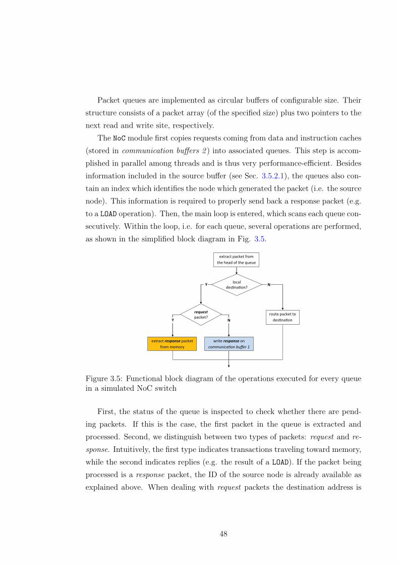
Packet queues are implemented as circular buffers of configurable size. Their
structure consists of a packet array (of the specified size) plus two pointers to the
next read and write site, respectively.
The NoC module first copies requests coming from data and instruction caches
(stored in communication buffers 2 ) into associated queues. This step is accom-
plished in parallel among threads and is thus very performance-efficient. Besides
information included in the source buffer (see Sec. 3.5.2.1), the queues also con-
tain an index which identifies the node which generated the packet (i.e. the source
node). This information is required to properly send back a response packet (e.g.
to a LOAD operation). Then, the main loop is entered, which scans each queue con-
secutively. Within the loop, i.e. for each queue, several operations are performed,
as shown in the simplified block diagram in Fig. 3.5.
local
des!na!on?
extract packet from
the head of the queue
request
packet? route packet to
des!na!on
write response on
communica�on buffer 1
extract response packet
from memory
N Y
N Y
Figure 3.5: Functional block diagram of the operations executed for every queuein a simulated NoC switch
First, the status of the queue is inspected to check whether there are pend-
ing packets. If this is the case, the first packet in the queue is extracted and
processed. Second, we distinguish between two types of packets: request and re-
sponse. Intuitively, the first type indicates transactions traveling toward memory,
while the second indicates replies (e.g. the result of a LOAD). If the packet being
processed is a response packet, the ID of the source node is already available as
explained above. When dealing with request packets the destination address is
48
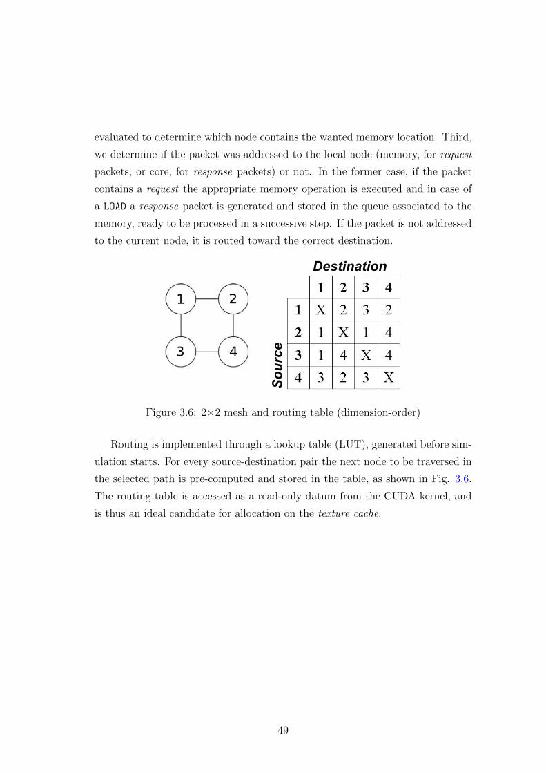
evaluated to determine which node contains the wanted memory location. Third,
we determine if the packet was addressed to the local node (memory, for request
packets, or core, for response packets) or not. In the former case, if the packet
contains a request the appropriate memory operation is executed and in case of
a LOAD a response packet is generated and stored in the queue associated to the
memory, ready to be processed in a successive step. If the packet is not addressed
to the current node, it is routed toward the correct destination.
DestinationSource
Figure 3.6: 2×2 mesh and routing table (dimension-order)
Routing is implemented through a lookup table (LUT), generated before sim-
ulation starts. For every source-destination pair the next node to be traversed in
the selected path is pre-computed and stored in the table, as shown in Fig. 3.6.
The routing table is accessed as a read-only datum from the CUDA kernel, and
is thus an ideal candidate for allocation on the texture cache.
49
3.6 Experimental Results
In this section we evaluate the performance of our simulator. The experiment re-
sults are obtained using a Nvidia GeForce GTX 480 CUDA-compliant video card
mounted on a workstation with an Intel i7 CPU at 2.67 GHz running Ubuntu
Linux OS. We carried out three different kind of experiments with our simulator.
The first set of experiments is aimed at measuring the simulation time breakdown
among system components, i.e. the percentage of the simulation time spent over
cores, caches, NoC for different instruction types in the ISA. As a second set of ex-
periments we evaluate the performance of our simulator – in terms of simulated
MIPS – using real-world benchmarks and considering different target architec-
tural design variants. Finally, we provide a comparison between the performance
of our simulator and OVPSim (Open Virtual platform Simulator)
3.6.1 Simulation time breakdown
Since we can model different system components in our simulator (i.e. cores, I-
cache, D-caches and on-chip network), it is important to understand the amount
of time spent in simulating each of them.
For these evaluations, we considered a single-tile architecture composed of
just one core equipped with both instructions and data caches, and a network
switch connected to the main memory. We measured the cost of simulating each
type of three main instructions classes, namely arithmetic/logic, control flow and
memory instructions.
We considered two different granularities for our breakdown analysis. The first
experiment has been conducted at the system level, and was meant to estimate
the cost of modeling each component of the simulator. This allows to better
understand where most of the simulation time is spent (i.e. which component
is heaviest to simulate). The second analysis takes a closer look inside the core
model to estimate the cost due to the simulation of each stage of the pipeline (i.e.
fetch, decode and execute). In all experiments we measured the amount of host
clock cycles spent to simulate each component or each stage of the pipeline.
50
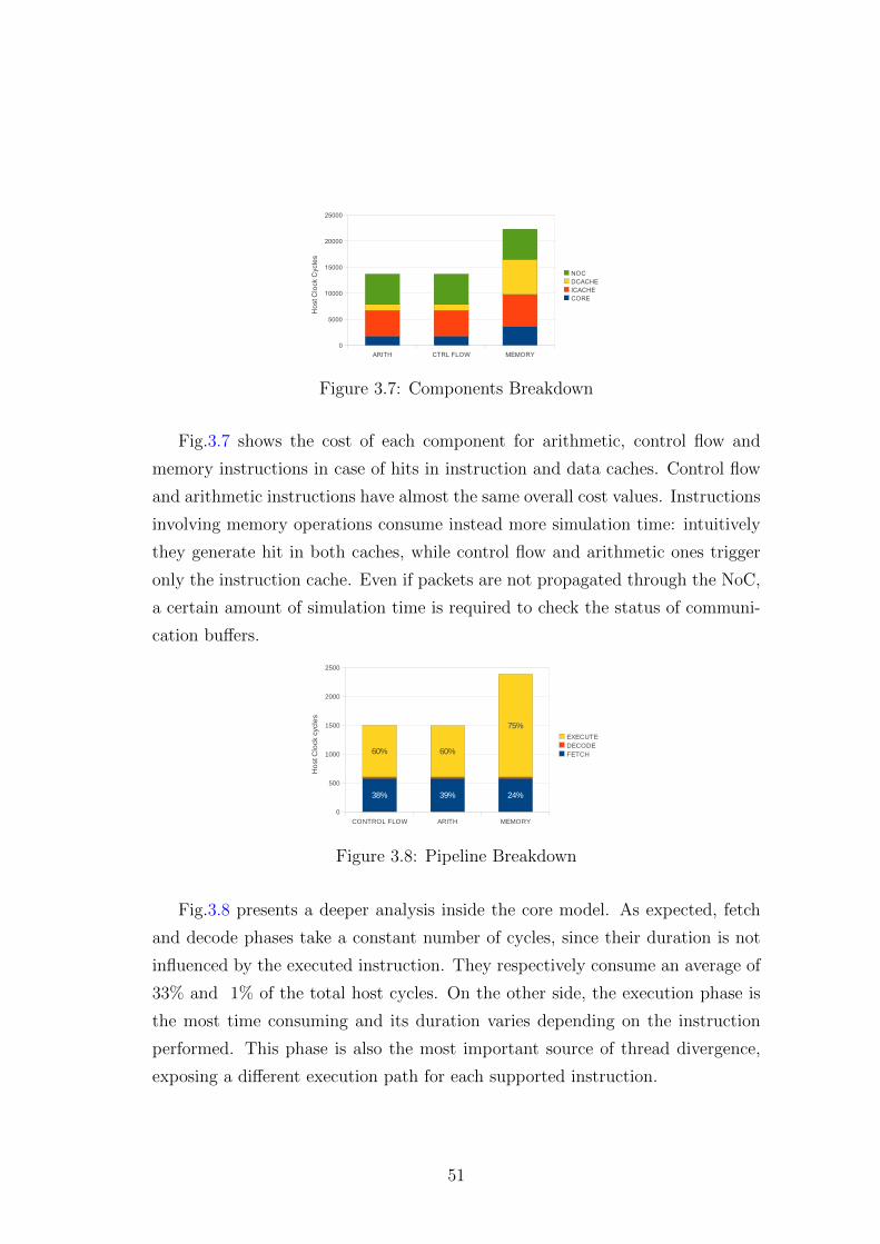
Figure 3.7: Components Breakdown
Fig.3.7 shows the cost of each component for arithmetic, control flow and
memory instructions in case of hits in instruction and data caches. Control flow
and arithmetic instructions have almost the same overall cost values. Instructions
involving memory operations consume instead more simulation time: intuitively
they generate hit in both caches, while control flow and arithmetic ones trigger
only the instruction cache. Even if packets are not propagated through the NoC,
a certain amount of simulation time is required to check the status of communi-
cation buffers.
Figure 3.8: Pipeline Breakdown
Fig.3.8 presents a deeper analysis inside the core model. As expected, fetch
and decode phases take a constant number of cycles, since their duration is not
influenced by the executed instruction. They respectively consume an average of
33% and 1% of the total host cycles. On the other side, the execution phase is
the most time consuming and its duration varies depending on the instruction
performed. This phase is also the most important source of thread divergence,
exposing a different execution path for each supported instruction.
51
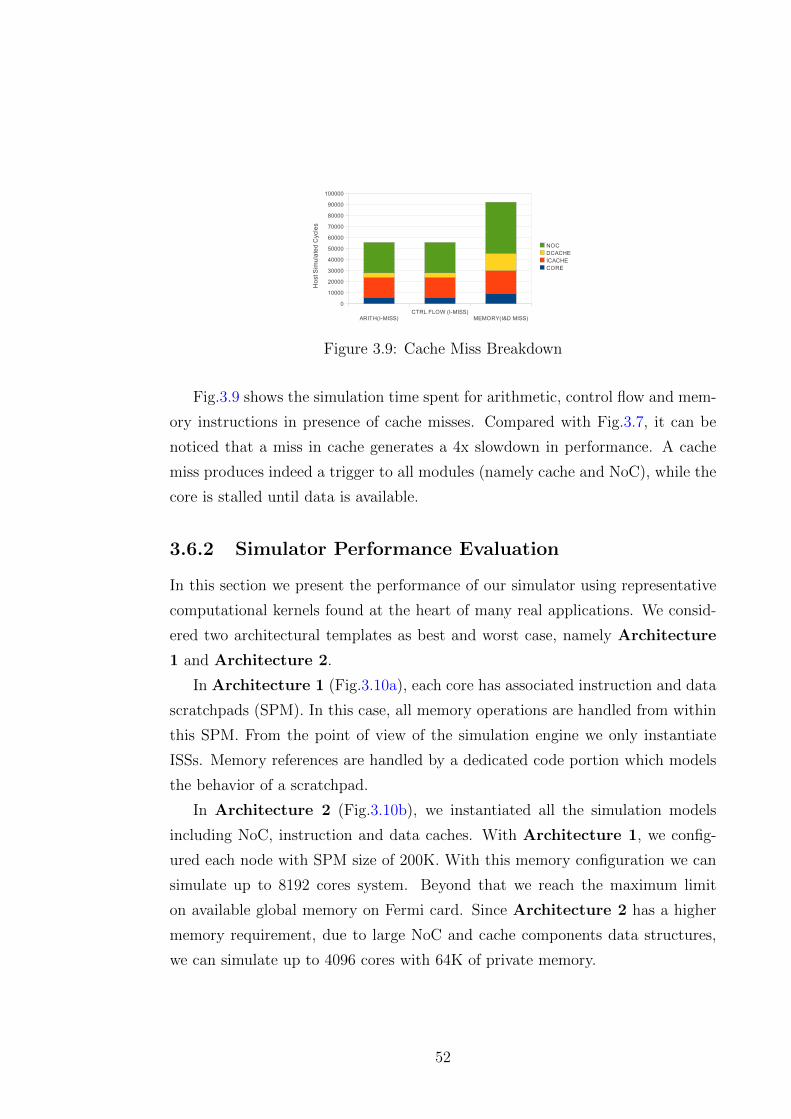
Figure 3.9: Cache Miss Breakdown
Fig.3.9 shows the simulation time spent for arithmetic, control flow and mem-
ory instructions in presence of cache misses. Compared with Fig.3.7, it can be
noticed that a miss in cache generates a 4x slowdown in performance. A cache
miss produces indeed a trigger to all modules (namely cache and NoC), while the
core is stalled until data is available.
3.6.2 Simulator Performance Evaluation
In this section we present the performance of our simulator using representative
computational kernels found at the heart of many real applications. We consid-
ered two architectural templates as best and worst case, namely Architecture
1 and Architecture 2.
In Architecture 1 (Fig.3.10a), each core has associated instruction and data
scratchpads (SPM). In this case, all memory operations are handled from within
this SPM. From the point of view of the simulation engine we only instantiate
ISSs. Memory references are handled by a dedicated code portion which models
the behavior of a scratchpad.
In Architecture 2 (Fig.3.10b), we instantiated all the simulation models
including NoC, instruction and data caches. With Architecture 1, we config-
ured each node with SPM size of 200K. With this memory configuration we can
simulate up to 8192 cores system. Beyond that we reach the maximum limit
on available global memory on Fermi card. Since Architecture 2 has a higher
memory requirement, due to large NoC and cache components data structures,
we can simulate up to 4096 cores with 64K of private memory.
52
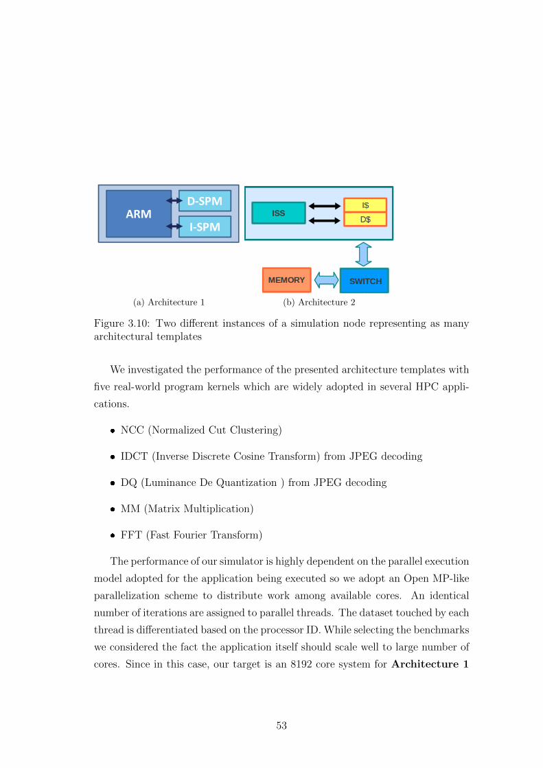
ARM
D-SPM
I-SPM
(a) Architecture 1 (b) Architecture 2
Figure 3.10: Two different instances of a simulation node representing as manyarchitectural templates
We investigated the performance of the presented architecture templates with
five real-world program kernels which are widely adopted in several HPC appli-
cations.
� NCC (Normalized Cut Clustering)
� IDCT (Inverse Discrete Cosine Transform) from JPEG decoding
� DQ (Luminance De Quantization ) from JPEG decoding
� MM (Matrix Multiplication)
� FFT (Fast Fourier Transform)
The performance of our simulator is highly dependent on the parallel execution
model adopted for the application being executed so we adopt an Open MP-like
parallelization scheme to distribute work among available cores. An identical
number of iterations are assigned to parallel threads. The dataset touched by each
thread is differentiated based on the processor ID. While selecting the benchmarks
we considered the fact the application itself should scale well to large number of
cores. Since in this case, our target is an 8192 core system for Architecture 1
53
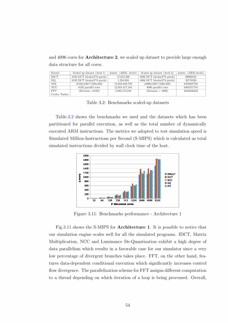
and 4096 cores for Architecture 2, we scaled up dataset to provide large enough
data structure for all cores.
Kernel Scaled up dataset (Arch 1) #instr. (ARM, Arch1) Scaled up dataset (Arch 2) #instr. (ARM,Arch1)
IDCT 8192 DCT blocks(8*8 pixels) 17,813,586 4096 DCT blocks(8*8 pixels) 89069184DQ 8192 DCT blocks(8*8 pixels) 1,294,903 4096 DCT blocks(8*8 pixels) 20719328MM (8192x100)*(100x100) 12,916,049,728 (4096x100)*(100x100) 6458025792NCC 8192 parallel rows 12,954,417,184 4096 parallel rows 6405371744FFT (Datasize =8192) 5,689,173,216 (Datasize = 4096) 2844638432Cooley-Turkey
Table 3.2: Benchmarks scaled-up datasets
Table.3.2 shows the benchmarks we used and the datasets which has been
partitioned for parallel execution, as well as the total number of dynamically
executed ARM instructions. The metrics we adopted to test simulation speed is
Simulated Million-Instructions per Second (S-MIPS) which is calculated as total
simulated instructions divided by wall clock time of the host.
Figure 3.11: Benchmarks performance - Architecture 1
Fig.3.11 shows the S-MIPS for Architecture 1. It is possible to notice that
our simulation engine scales well for all the simulated programs. IDCT, Matrix
Multiplication, NCC and Luminance De-Quantization exhibit a high degree of
data parallelism which results in a favorable case for our simulator since a very
low percentage of divergent branches takes place. FFT, on the other hand, fea-
tures data-dependent conditional execution which significantly increases control
flow divergence. The parallelization scheme for FFT assigns different computation
to a thread depending on which iteration of a loop is being processed. Overall,
54
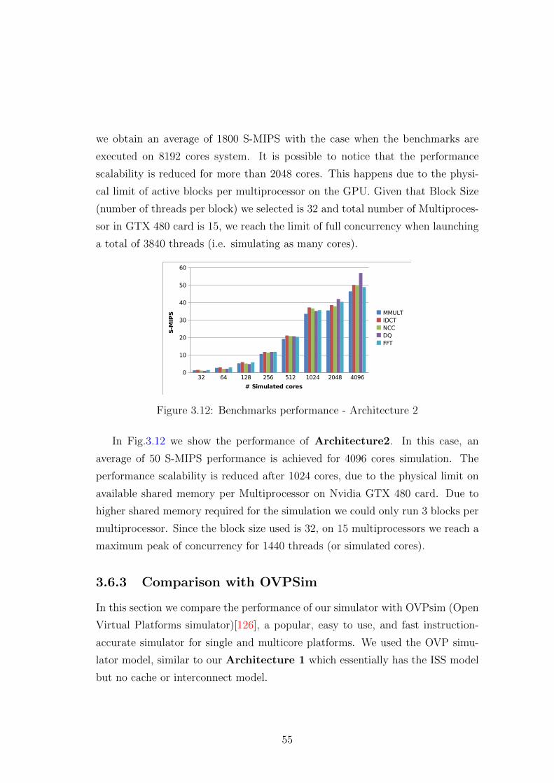
we obtain an average of 1800 S-MIPS with the case when the benchmarks are
executed on 8192 cores system. It is possible to notice that the performance
scalability is reduced for more than 2048 cores. This happens due to the physi-
cal limit of active blocks per multiprocessor on the GPU. Given that Block Size
(number of threads per block) we selected is 32 and total number of Multiproces-
sor in GTX 480 card is 15, we reach the limit of full concurrency when launching
a total of 3840 threads (i.e. simulating as many cores).
Figure 3.12: Benchmarks performance - Architecture 2
In Fig.3.12 we show the performance of Architecture2. In this case, an
average of 50 S-MIPS performance is achieved for 4096 cores simulation. The
performance scalability is reduced after 1024 cores, due to the physical limit on
available shared memory per Multiprocessor on Nvidia GTX 480 card. Due to
higher shared memory required for the simulation we could only run 3 blocks per
multiprocessor. Since the block size used is 32, on 15 multiprocessors we reach a
maximum peak of concurrency for 1440 threads (or simulated cores).
3.6.3 Comparison with OVPSim
In this section we compare the performance of our simulator with OVPsim (Open
Virtual Platforms simulator)[126], a popular, easy to use, and fast instruction-
accurate simulator for single and multicore platforms. We used the OVP simu-
lator model, similar to our Architecture 1 which essentially has the ISS model
but no cache or interconnect model.
55
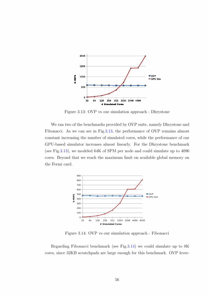
Figure 3.13: OVP vs our simulation approach - Dhrystone
We ran two of the benchmarks provided by OVP suite, namely Dhrystone and
Fibonacci. As we can see in Fig.3.13, the performance of OVP remains almost
constant increasing the number of simulated cores, while the performance of our
GPU-based simulator increases almost linearly. For the Dhrystone benchmark
(see Fig.3.13), we modeled 64K of SPM per node and could simulate up to 4096
cores. Beyond that we reach the maximum limit on available global memory on
the Fermi card.
Figure 3.14: OVP vs our simulation approach - Fibonacci
Regarding Fibonacci benchmark (see Fig.3.14) we could simulate up to 8K
cores, since 32KB scratchpads are large enough for this benchmark. OVP lever-
56
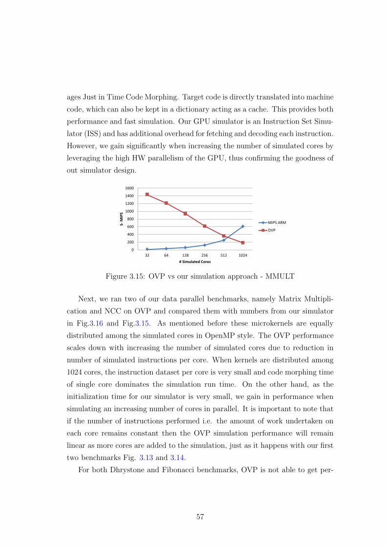
ages Just in Time Code Morphing. Target code is directly translated into machine
code, which can also be kept in a dictionary acting as a cache. This provides both
performance and fast simulation. Our GPU simulator is an Instruction Set Simu-
lator (ISS) and has additional overhead for fetching and decoding each instruction.
However, we gain significantly when increasing the number of simulated cores by
leveraging the high HW parallelism of the GPU, thus confirming the goodness of
out simulator design.
0
200
400
600
800
1000
1200
1400
1600
32 64 128 256 512 1024
S-
MIP
S
# Simulated Cores
MIPS ARM
OVP
Figure 3.15: OVP vs our simulation approach - MMULT
Next, we ran two of our data parallel benchmarks, namely Matrix Multipli-
cation and NCC on OVP and compared them with numbers from our simulator
in Fig.3.16 and Fig.3.15. As mentioned before these microkernels are equally
distributed among the simulated cores in OpenMP style. The OVP performance
scales down with increasing the number of simulated cores due to reduction in
number of simulated instructions per core. When kernels are distributed among
1024 cores, the instruction dataset per core is very small and code morphing time
of single core dominates the simulation run time. On the other hand, as the
initialization time for our simulator is very small, we gain in performance when
simulating an increasing number of cores in parallel. It is important to note that
if the number of instructions performed i.e. the amount of work undertaken on
each core remains constant then the OVP simulation performance will remain
linear as more cores are added to the simulation, just as it happens with our first
two benchmarks Fig. 3.13 and 3.14.
For both Dhrystone and Fibonacci benchmarks, OVP is not able to get per-
57
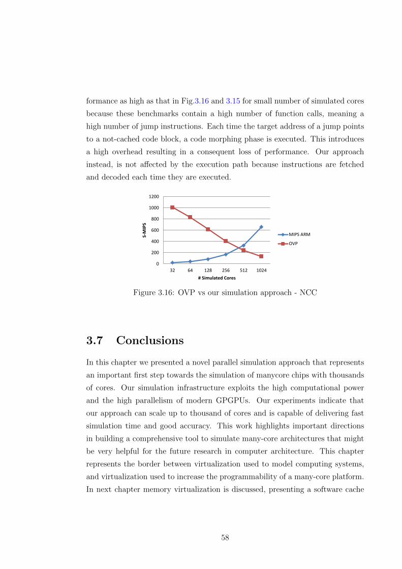
formance as high as that in Fig.3.16 and 3.15 for small number of simulated cores
because these benchmarks contain a high number of function calls, meaning a
high number of jump instructions. Each time the target address of a jump points
to a not-cached code block, a code morphing phase is executed. This introduces
a high overhead resulting in a consequent loss of performance. Our approach
instead, is not affected by the execution path because instructions are fetched
and decoded each time they are executed.
0
200
400
600
800
1000
1200
32 64 128 256 512 1024
S-M
IPS
# Simulated Cores
MIPS ARM
OVP
Figure 3.16: OVP vs our simulation approach - NCC
3.7 Conclusions
In this chapter we presented a novel parallel simulation approach that represents
an important first step towards the simulation of manycore chips with thousands
of cores. Our simulation infrastructure exploits the high computational power
and the high parallelism of modern GPGPUs. Our experiments indicate that
our approach can scale up to thousand of cores and is capable of delivering fast
simulation time and good accuracy. This work highlights important directions
in building a comprehensive tool to simulate many-core architectures that might
be very helpful for the future research in computer architecture. This chapter
represents the border between virtualization used to model computing systems,
and virtualization used to increase the programmability of a many-core platform.
In next chapter memory virtualization is discussed, presenting a software cache
58
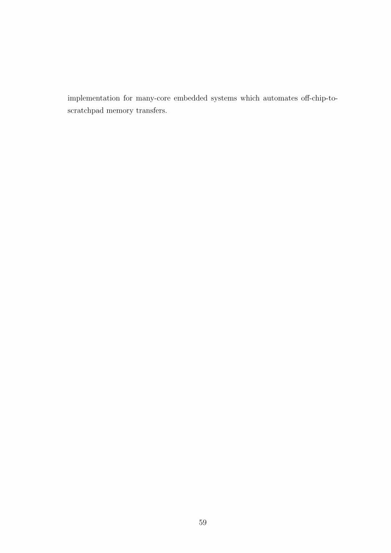
implementation for many-core embedded systems which automates off-chip-to-
scratchpad memory transfers.
59

60
Chapter 4
Memory Virtualization: Software
Caches
4.1 Overview
During the last decade we have seen an unprecedented technological growth in the
field of chip manufacturing and computing systems design. The main disruptive
change was the shift to multi-core systems [66], with the aim of increasing the
computational power provided by processors, while at the same time respecting
the always shrinking power budget imposed by the market [30]. Miniaturization
and multi-core processors allowed embedded systems with astonishing computa-
tional performance to be integrated in all-day life devices (e.g. smart-phones,
tablets), transforming several power demanding desktop applications (e.g. com-
puter vision applications, multimedia applications) into embedded applications.
The key feature of such embedded systems is power efficiency, in terms of high
computational power with a reduced power consumption, and has been addressed
with the introduction of Heterogeneous Multiprocessors Systems on a Chip (Het-
erogeneous MPSoC). Heterogeneous MPSoCs usually feature a complex multi-
core based processor alongside with power efficient, and architecturally simpler,
many-core general purpose accelerators (e.g. embedded GPUs) used to execute
parallel intensive kernels. Examples of such design are [33, 96, 107].
61
Off-the-shelf many-core accelerators are composed by hundreds of simple com-
putational units, and are expected to scale to up-to thousand of cores [30]. This
growth provides a very high efficiency in terms of GOPS/W but at the same time
increases the design effort. One common scheme to lower the design complexity
is the clustered architecture; computing units are packed in clusters. Multiple
clusters are placed in the same chip and communicate using on-chip interconnec-
tion mediums (e.g. Network-on-Chip), moving the design effort to the design of
a cluster. Even with this simplified design pattern power efficiency and area are
pressing constraints, and a common design choice is to avoid the use of per-core
data caches, replacing them with a fast per-cluster (or per-core) data scratch-pad.
Two examples of the above-mentioned design pattern are STHORM of STMi-
croelectronics [88] and the Cell Broadband Engine [100]. STHORM is an emerg-
ing many-core accelerator applying such a design pattern. It features clusters con-
nected through an asynchronous NoC, with each cluster equipped with up to 16
STxP70 cores and a shared multi-banked tightly coupled data memory (TCDM).
The Cell Broadband Engine features 8 Synergistic Processing Elements (SPE)
with private instruction cache, a private data scratch-pad and a DMA engine.
All the SPEs of the Cell processor communicate and access the external memory
using a ring bus.
Writing well-performing applications for both of the cited example architec-
tures, requires a non-negligible programming effort due to the lack of a data
cache. Even if the use of a data scratch-pad is more efficient than a cache (with
the same size in bytes a scratch-pad occupies ∼ 30% less area than a cache [20]),
it requires memory transfer from/to the off-chip external memory to be explic-
itly managed by applications. Off-chip DRAM memories have hundreds of clock
cycles access latency, and programmers usually need to hide that overhead with
complex Direct Memory Access (DMA) copy-in and copy-out transfer patterns.
DMA engines are used to overlap computation and communication applying pro-
gramming patterns like double-buffering. In applications using double buffering
the computation is divided in chunks, and while computing the actual chunk the
next one is being transferred by the DMA. Such a programming scheme is error
62
prone, and often forces programmers to rewrite almost the entire application to
be tailored to the DMA transfer strategy.
An alternative to exploit the speed of on-chip data scratch-pads are software
caches. A software cache is a runtime layer able to handle the entire scratch-pad
memory (or a subset of it) as if it were a hardware cache, hiding to the program-
mer all memory transfers between on-chip and off-chip memory. Differently from
a hardware cache, a software cache has a higher flexibility in terms of configu-
ration of parameters (e.g. line size, total size, associativity), and also in terms
of choosing the best replacement policy or organization of internal structures.
However its performance is generally lower than that of a hardware cache.
Software caches are not new to the research community, and different ap-
proaches have been proposed for scratch-pad based multi-core systems. Most of
the previous work has been done mainly for the Cell BE processor, in which each
synergistic processing element (SPE) [58] has a private (aliased) data scratch-
pad memory space. SPEs in the Cell processor do not interfere during an ac-
cess in software cache, and concurrency is resolved at the external memory level
when writing back a cache line or bringing it inside the software cache. Correct-
ness of memory accesses is ensured using DMA lists, forcing the correct ordering
between DMA operations, or through software libraries implementing coherent
shared memory abstractions [19, 116].
In this chapter we present a software cache implementation for a cluster of
the STMicroelectronics STHORM acceleration fabric, in which the scratch-pad
memory is shared between the 16 cores in the cluster. Contention in accessing
the software cache happens inside the same cluster, and parallel accesses need
to be regulated. We exploited the hardware features provided by the platform
like the multi-bank structure of the TCDM, and the hardware for fast inter-core
synchronization. Moreover, looking at modern applications, we have seen that
most multimedia and computer vision kernels work with multi-byte objects (e.g.
feature descriptors), instead of working on single memory elements. We exploited
this peculiarity to further optimize our software cache runtime, supporting the
lookup of entire objects within a single cache access. The overhead of the software
63
cache can be thus amortized by an entire application object, minimizing its global
impact on applications.
The main contributions of this chapter can be summarized as follows:
� Design of a thread-safe software cache: unlike in the Cell BE processor,
cores in a STHORM cluster share the same TCDM memory. Concurrent
accesses to the software cache must be controlled to ensure the correctness
of each memory access.
� Exploitation of hardware features of a STHORM cluster: use of
hardware for fast synchronization. Exploitation of the multi-bank TCDM
to allow parallel accesses to different lines of the cache.
� Minimization of look-up overhead: highly optimized C implementation
exploiting conditional instructions.
� Exploration of object oriented caching techniques: we implemented
an optimized version of the software cache able to deal with whole objects
instead of single memory words. We provide the use cases of the Face
Detection [131] and Normalized Cross Correlation (NCC) [83].
� Definition of a programming interface allowing the programmer to
define a cacheable object.
Our implementation has been validated with a set of micro-benchmarks, designed
to highlight specific aspects of our software cache, and with three case studies
coming from the computer vision world. In two of the three use cases presented
results are extracted from the first silicon implementation of the STHORM fabric.
The rest of the chapter is organized as follows: in section 4.2 we present
related work. In sections 4.3 and 4.4 we present respectively the implementation
of our software cache and the object oriented extensions. Experimental results
are presented in section 4.5. We conclude the chapter in section 4.6.
64
4.2 Related work
Software caches have always interested the research community as a tool to ease
the job of the programmer, allowing at the same time the efficient exploitation
of the entire memory hierarchy of a device without the need of heavy re-work
of existing applications. Early work on software caching appeared to reduce the
execution time in I/O intensive applications: in [128] the authors proposed a soft-
ware caching scheme to hide latencies due to I/O operations depending on disk
workload. Authors in [53] used software caching techniques for virtual memory
paging to hide the DRAM latency: in this context a software implementation can
take more complex decisions based on memory references of an application. Au-
thors in [90] propose a software-based instruction caching technique for embedded
processors without caching hardware, where the software manages a scratch-pad
memory as an instruction cache. Our implementation takes a different approach
by focusing on data caching. In [61] a second level software cache implementation
and a novel line replacement algorithm are presented, along with results showing
that a software cache implementation can be competitive with a hardware cache
implementation, especially with growing DRAM access latencies. The goal of
that work is similar to what we propose, hiding the DRAM latency, but we are
targeting a shared first level data cache in a multi-core system.
Another possible alternative for hiding the off-chip memory latency is data
prefetching [34]. Depending on the memory access pattern of an application,
data can be prefetched from the off-chip memory into the cache of the processor.
Prefetching techniques rely on compiler support, by analyzing the memory access
pattern and programming memory transfers towards closer (with respect to the
processor) memory buffers. Authors in [12] compare prefetching and software
caching for search applications, with the aim of reducing the miss rate in the
data cache of the processor. They discovered that prefetching leads to a higher
number of instructions executed, and increases the memory traffic. Moreover,
prefetched data can replace data already in the data cache of the processor,
thereby increasing the miss rate. Software caches provide more flexibility, allowing
the programmer to selectively cache the data structures which suffer the most
65
from the external memory latency. Another important observation made by the
authors is that: the combination of prefetching and software caching can further
improve the benefits obtained with only the software cache.
The interest in software caches increased with the advent of multi-core chips
where, to increase energy and power efficiency, cores are often equipped with a
private or shared data scratch-pad memory instead of a data cache. A first ex-
ample is [93], where authors provide an implementation of software cache for the
MIT Raw Machine, a parallel tiled processor. Each tile of the Raw Machine is
composed of a RISC computing unit and a small SRAM for both instructions
and data. In that work, authors present a software caching based virtual mem-
ory system, to cope the limited size of the on-chip SRAM memory, and hide the
external memory latency. The runtime also relies on the support of the compiler,
which is able to resolve some memory references at the compile time, and place
data structures directly in the SRAM memory. Also, with the aim of minimiz-
ing the number of cache look-ups, the compiler is able to reuse previous virtual
address translations. In contrast this work does not rely on the support of the
compiler, and we are target a system with a data scratch-pad shared amongst
the 16 processors in a STHORM cluster.
There has been a lot of related work targeting the Cell BE processor, which
was the first commercial device applying the design patterns discussed in the
introduction. Authors in [17] proposed an extension to the Cell SPE pipeline
adding a new instruction into the instruction set, to handle in hardware the
lookup procedure as it represents the most critical path of a cache. Only in case
of a cache miss does the access in cache involve a software routine. Instead,
in this work we maintain a software lookup procedure which has been heavily
optimized, exploiting STxP70 special instructions and compiler optimizations.
In [18] the authors describe the implementation of a software cache oriented to
multidimensional memory objects. Authors observed the access pattern of several
multimedia applications, and saw that most of them access multidimensional
data structures. The cache design proposed in [18] handles data mimicking their
logical organization. In [37] the authors describe a prefetching system, based on
66
application runtime access patterns for a software cache on the Cell BE processor,
which is complementary to our work. Prefetching, in fact, is a technique which
can be used to further optimize software cache implementations.
In a platform similar to STHORM many-core accelerator of STMicroelectron-
ics [27, 88], processors inside the same cluster share a single data scratch-pad
memory, and software cache accesses must be regulated in order to avoid data
races. Most previous work on software caches use the Cell BE processor as a
target architecture, where no concurrency happens when accessing the software
cache. The only possible concurrency happens in the external shared memory.
Most approaches rely on an already available coherent shared memory abstraction
or on DMA lists. Authors in [116] describe a software cache implementation with
a novel design called Extended Set-Index Cache (ESC) for the Cell BE processor,
in which the number of tag entries is bigger than the number of lines, with the
aim of reducing the miss rate. In [116] the shared memory abstraction is given by
COMIC [78], a software library able to provide a coherent shared memory view
to all SPEs in the Cell processor.
Authors in [19] present a software cache implementation where operations
of line refill or line write back are handled via DMA transfers. In that case the
concurrency on the external memory is resolved using DMA lists. The correctness
of transactions is ensured by never reordering the write back followed by a refill of
the same cache line. In [36] the authors present a software cache implementation
of the OpenMP model for multi-core and many-core systems, but no discussion
is included on possible concurrent accesses to the external memory. The authors
instead leverage on the weak consistency memory model of OpenMP, in which a
shared variable is not forced to be consistent with the copy in external memory,
until a memory barrier is reached.
Another interesting aspect of software managed caches is the possibility of
exploiting compiler support. Authors in [56] [50] presented a set of compile
time optimizations able to identify access patterns, unroll loops or reorder cache
references without the intervention of the programmer. This kind of compiler
support is complementary to our software cache design proposal, and has to be
67
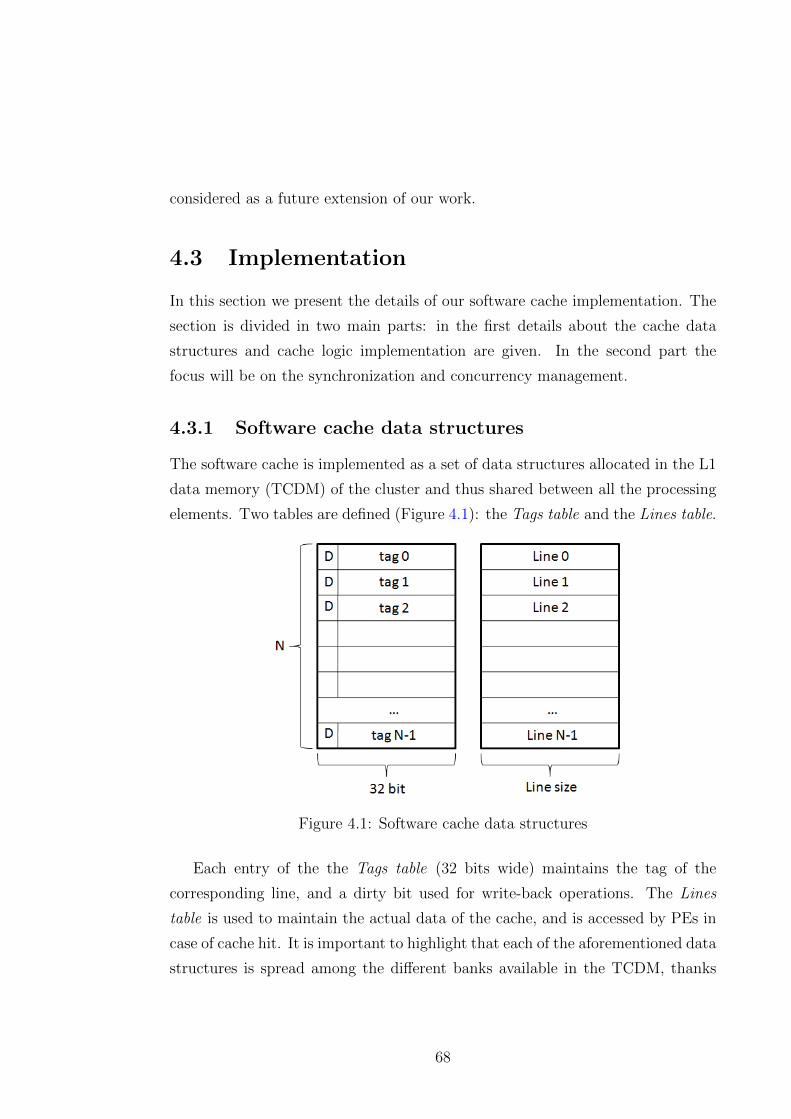
considered as a future extension of our work.
4.3 Implementation
In this section we present the details of our software cache implementation. The
section is divided in two main parts: in the first details about the cache data
structures and cache logic implementation are given. In the second part the
focus will be on the synchronization and concurrency management.
4.3.1 Software cache data structures
The software cache is implemented as a set of data structures allocated in the L1
data memory (TCDM) of the cluster and thus shared between all the processing
elements. Two tables are defined (Figure 4.1): the Tags table and the Lines table.
Figure 4.1: Software cache data structures
Each entry of the the Tags table (32 bits wide) maintains the tag of the
corresponding line, and a dirty bit used for write-back operations. The Lines
table is used to maintain the actual data of the cache, and is accessed by PEs in
case of cache hit. It is important to highlight that each of the aforementioned data
structures is spread among the different banks available in the TCDM, thanks
68
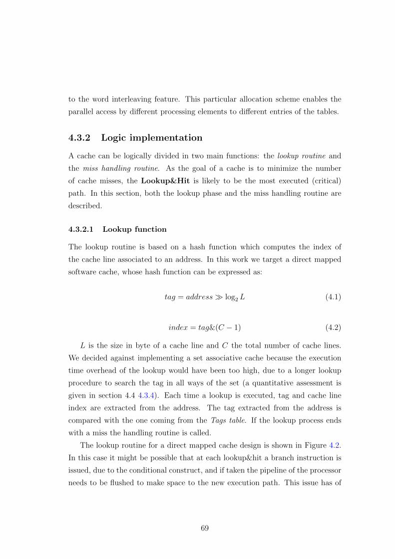
to the word interleaving feature. This particular allocation scheme enables the
parallel access by different processing elements to different entries of the tables.
4.3.2 Logic implementation
A cache can be logically divided in two main functions: the lookup routine and
the miss handling routine. As the goal of a cache is to minimize the number
of cache misses, the Lookup&Hit is likely to be the most executed (critical)
path. In this section, both the lookup phase and the miss handling routine are
described.
4.3.2.1 Lookup function
The lookup routine is based on a hash function which computes the index of
the cache line associated to an address. In this work we target a direct mapped
software cache, whose hash function can be expressed as:
tag = address� log2 L (4.1)
index = tag&(C − 1) (4.2)
L is the size in byte of a cache line and C the total number of cache lines.
We decided against implementing a set associative cache because the execution
time overhead of the lookup would have been too high, due to a longer lookup
procedure to search the tag in all ways of the set (a quantitative assessment is
given in section 4.4 4.3.4). Each time a lookup is executed, tag and cache line
index are extracted from the address. The tag extracted from the address is
compared with the one coming from the Tags table. If the lookup process ends
with a miss the handling routine is called.
The lookup routine for a direct mapped cache design is shown in Figure 4.2.
In this case it might be possible that at each lookup&hit a branch instruction is
issued, due to the conditional construct, and if taken the pipeline of the processor
needs to be flushed to make space to the new execution path. This issue has of
69
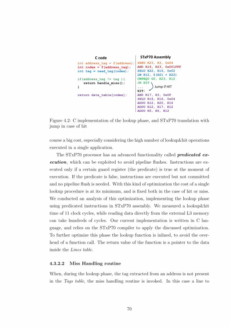
int address_tag = f(address);
int index = f(address_tag);
int tag = read_tag(index);
if(address_tag != tag ){
return handle_miss();
}
return data_table[index];
C code
SHRU R23, R3, 0x04
AND R16, R23, 0x001FFF
SHLU R22, R16, 0x02
LW R12, @(R21 + R22)
CMPEQU G0, R23, R12
JR HIT
...
HIT:
AND R17, R3, 0x0F
SHLU R16, R16, 0x04
ADDU R12, R20, R16
ADDU R12, R17, R12
ADDU R5, R5, R12
STxP70 Assembly
Jump if HIT
Figure 4.2: C implementation of the lookup phase, and STxP70 translation withjump in case of hit
course a big cost, especially considering the high number of lookup&hit operations
executed in a single application.
The STxP70 processor has an advanced functionality called predicated ex-
ecution , which can be exploited to avoid pipeline flushes. Instructions are ex-
ecuted only if a certain guard register (the predicate) is true at the moment of
execution. If the predicate is false, instructions are executed but not committed
and no pipeline flush is needed. With this kind of optimization the cost of a single
lookup procedure is at its minimum, and is fixed both in the case of hit or miss.
We conducted an analysis of this optimization, implementing the lookup phase
using predicated instructions in STxP70 assembly. We measured a lookup&hit
time of 11 clock cycles, while reading data directly from the external L3 memory
can take hundreds of cycles. Our current implementation is written in C lan-
guage, and relies on the STxP70 compiler to apply the discussed optimization.
To further optimize this phase the lookup function is inlined, to avoid the over-
head of a function call. The return value of the function is a pointer to the data
inside the Lines table.
4.3.2.2 Miss Handling routine
When, during the lookup phase, the tag extracted from an address is not present
in the Tags table, the miss handling routine is invoked. In this case a line to
70
be evicted is selected, according to the replacement policy. For a direct mapped
cache, the replacement policy is trivial, as each memory line can be stored in only
one cache line. Once the victim is selected, the dirty bit in the corresponding
entry of the Tags table is checked. If the dirty bit is asserted the line has been
modified, and has to be written back to external memory. The write-back address
of each line is computed from the tag as: tag � LG2 LINE SIZE. At the end
of this procedure the line requested can be copied inside the Lines Table, and the
address of the requested data returned to the application. Refill and writeback
are synchronous operations, which use the DMA engine of each STHORM cluster
to move lines back and forth from external memory. One DMA transfer is issued
for each refill or writeback. We decided to use the DMA even if the transfers
are synchronous, because DMA transfers are faster than explicit accesses to the
external memory. From the profiling done on the STHORM chip, we measured
that a single external-memory-to-TCDM transfer (4 bytes word) has a cost of
∼ 370 cycles. Thus, the refill of a cache line of 32 bytes takes a total time of
∼ 2960 cycles. On the other hand, using the DMA the transfer time for a block
of 32 bytes is ∼ 670 cycles.
4.3.3 Concurrency management
As introduced in Section 4.3.1, all the software cache data structures are allocated
into the shared TCDM memory, implying possible concurrent accesses by all
Processing Elements (PEs) in the cluster. To avoid any possible race condition
between PEs, which can lead to wrong management of the cache or to wrong data
accesses, all data structures of the cache have to be protected from concurrent
accesses.
Consider the case when a PE asking for an address lookup gets a hit, but before
receiving the data another PE gets a miss on the same line (conflict miss). Given
that the Lines and Tags tables are shared, the first PE can receive the wrong data
due to an overlap of the two accesses. The easiest way to overcome the problem is
to protect the entire cache structure with a critical region. Each time a PE issues
a lookup request the cache is locked and no other PE can use it until the end of
71
the lookup, making our implementation thread safe. Even if this solution solves
the concurrency problem, it also opens an important optimization possibility:
even if PEs need to lookup addresses whose entries in the Tags table reside in
different banks, they cannot access those lines parallel because the critical section
is protecting the entire software cache.
To fully optimize and exploit the multi-banked structure of the TCDM mem-
ory, we decided to implement a line lock mechanism allowing each processor to
lock only the line requested during the lookup phase. Other processors are then
free to access in parallel (when possible) any other line of the cache. Each time
a lookup is executed the PE first checks the lock location associated with the
target line (see Figure 4.3). If the lock has already been taken by any other PE,
the current PE is blocked, until the line becomes free again. The waiting phase
is implemented as a polling routine over the lock.
Figure 4.3: Parallel access to the Tags table
To implement a lock it is possible to exploit two different facilities of the
STHORM fabric: the Hardware Synchronizer (HWS) or the hardware Test and
Set (T&S) mechanism. In the former an atomic counter is associated with each
lock. Each time a PE wants to acquire a lock it has to use the atomic increment
function, which in addition to the increment reads also the current value of the
counter. If the value is bigger than zero the lock is already taken, otherwise the
lock is free and the increment will lock it. In the second implementation each
72
lock is represented by a T&S location, a choice which requires the allocation
of an additional data structure (the Locks table) in the TCDM with as many
entries as lines in the cache. Reading from a T&S address fills the memory
location associated to the lock of 1 bits, and reads the value atomically. If when
reading the value is bigger than zero the lock is already taken, otherwise the read
operation will lock it.
Both implementations offer the same functionality, but even if the T&S solu-
tion requires the allocation of an additional data structure it is preferable to the
HWS solution for two main reasons:
� reading a T&S location is faster than incrementing an atomic counter;
mainly related to the HWS API.
� for the line lock implementation there are not enough atomic counters to
protect each line of the cache.
In Section 4.5.3 a comparison between each implementation (Cache lock, Line
lock), with both HWS and T&S locks is discussed.
4.3.4 Direct-mapped vs set-associative software cache
As stated in paragraph 4.3.2.1 we decided to implement a direct-mapped cache,
and ruled out a set associative design. In fact, even if set associativity may
reduce the number of conflict misses, it also introduces a substantial execution
time overhead. We measured such overhead for a 4-way set associative cache
using an ISS of the STxP70 processor. The lookup&hit path uses 14 instruction
bundles for a direct-mapped design, compared to 26 for a 4-way set associative
one. The increased overhead is due to the extra lookup operations (2 bundles
per set), and to the additional lock needed to manage the replacement policy
(e.g. LRU). Lines in the same set in fact share the information needed for the
replacement policy (e.g. LRU bits), which is updated at each access to a line of
the set. The update phase implies an additional lock, and the actual update of the
information. Acquiring a lock introduces 4 extra instruction bundles (3 to acquire
the lock and one to release), and the actual update operation introduces 2 extra
73
bundles (2 memory accesses and one arithmetic operation). The combination
of these factors counteracts the benefits of the set associativity, due to a 85%
overhead.
4.4 Object Oriented caching extensions
Despite their ease of use, software caches may incur non-negligible overheads
due to their software nature. In fact, each memory access performed using the
software cache adds an inherent overhead, due to the lookup of the memory
reference.
A large number of applications work on multi-byte objects, instead of working
on single memory elements. This gives the opportunity for optimization, with the
goal of reducing the lookup overhead.
1 for ( x = x s ; x < x s + x e ; x++) {2 for ( y = y s ; y < y s + y e ; y++) {3 char p = img in [ x + y * img width ] ;
4 for ( i =0; i < N; i++)
5 f ( v ) ;
6 }7 }
Listing 4.1: Example of computer vision kernel
Code listing 4.1 shows the typical implementation of the innermost loop of
a vision kernel. In this example the image is scanned row by row, and at each
row a certain number (y e) of adjacent pixels is accessed, with some computation
done on each pixel (represented by the for loop of N iterations). Programmers
would cache the content of img in as it is residing in external memory, replacing
the memory access at line 3 with a software cache access.
1 for ( x = x s ; x < x s + x e ; x++) {2 for ( y = y s ; y < y s + y e ; y++) {3 char v = cache read char(&img in[x + y * img width]);
4 for ( i =0; i < N; i++)
5 f ( v ) ;
74
6 }7 }
Listing 4.2: Example of computer vision kernel modified to use the software
cache
Code listing 4.2 shows the loop modified to use the software cache in the
standard way: each memory access to the buffer in external memory (img in) is
substituted by a software cache access. The code in listing 4.2 is going to be faster
than the one in listing 4.1, because accessing adjacent pixels is possible to benefit
from several cache hits. Nonetheless, code in listing 4.2 have a high number of
cache accesses, introducing a big overhead due to contention in TCDM. Consider
for example an application working on objects of 32 bytes. If the application
makes a cache access per byte of the object, it will issue a total number of 32
software cache accesses per object. Each cache lookup implies to access various
data structures in the TCDM (line locks, tags table) which may lead to conflicts
in the TCDM itself, due to different processors trying to access the same data
structures.
We consider an object as an abstract data structure composed of a block of
contiguous bytes, which is treated by the cache as a single entity. Our idea is to
map one object to a cache line, and to trigger a single lookup for an entire object.
Subsequent bytes are accessed directly from the Lines Table of the software cache,
without further triggering the lookup logic. With this alternative usage, the single
lookup operation can be amortized from an entire object, and the whole software
cache overhead is significantly reduced. Using the object cache is in fact possible
to mitigate any overhead due to conflicts in TCDM for the cache-handling data
structures. A good case study is represented by computer vision applications, a
well known and widely used class of computational intensive kernels [32]. Vision
kernels are often applied to pairs of objects, and involve all the bytes composing
each object.
At each software cache lookup the programmer gets as a result a copy of the
requested data, and puts it into the stack of the processor (or a register). The
same pattern is applied to entire objects: at each lookup a copy of the object is
75
created in the stack of the processor. While copying the object from the cache to
the stack it may happen that another processor is overriding that particular cache
line (conflict miss), leading to a possible wrong access. To avoid this problem we
slightly modified the lookup function, in order to keep the lock associated to the
actual line busy until the copy of the object is finished. This locking mechanism is
completely thread safe because all the locks are hidden behind the software cache
structure, and it can not happen that two processors involved in a rendez-vous
are waiting for the same lock.
Code in listing 4.3 shows how the object caching example can be applied to
code in listing 4.2. At line 2 the reference to the current object is taken from
cache, then the computation is performed in lines 3-6. At line 7 the lock of the
object is released.
It is important to notice that object caching is not a panacea. In fact, if
the amount of computation performed on each element of the object is high
(the value of N in the example), the object will be kept busy for a long time.
Other processors needing the object are then stalled until it becomes free again,
counteracting the benefits of object caching. This blocking effect is less severe
with line caching, because lines are freed immediately after the cache access (i.e.
the line is kept busy for a short time). The object oriented extension is evaluated
in Section 4.5.5.
1 for ( x = x s ; x < x s + x e ; x++) {2 char * v = cache obj ref(&img in[x + y s * img width]);
3 for ( y = 0 ; y < y e ; y++) {4 for ( i =0; i < N; i++)
5 f ( v [ y ] ) ;
6 }7 cache release obj(&img in[x + y s * img width]);
8 }
Listing 4.3: Example of computer vision kernel modified to use the object
cache
76
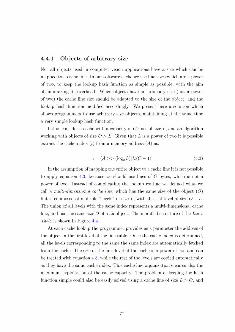
4.4.1 Objects of arbitrary size
Not all objects used in computer vision applications have a size which can be
mapped to a cache line. In our software cache we use line sizes which are a power
of two, to keep the lookup hash function as simple as possible, with the aim
of minimizing its overhead. When objects have an arbitrary size (not a power
of two) the cache line size should be adapted to the size of the object, and the
lookup hash function modified accordingly. We present here a solution which
allows programmers to use arbitrary size objects, maintaining at the same time
a very simple lookup hash function.
Let us consider a cache with a capacity of C lines of size L, and an algorithm
working with objects of size O > L. Given that L is a power of two it is possible
extract the cache index (i) from a memory address (A) as:
i = (A >> (log2 L))&(C − 1) (4.3)
In the assumption of mapping one entire object to a cache line it is not possible
to apply equation 4.3, because we should use lines of O bytes, which is not a
power of two. Instead of complicating the lookup routine we defined what we
call a multi-dimensional cache line, which has the same size of the object (O)
but is composed of multiple ”levels” of size L, with the last level of size O − L.
The union of all levels with the same index represents a multi-dimensional cache
line, and has the same size O of a an object. The modified structure of the Lines
Table is shown in Figure 4.4.
At each cache lookup the programmer provides as a parameter the address of
the object in the first level of the line table. Once the cache index is determined,
all the levels corresponding to the same the same index are automatically fetched
from the cache. The size of the first level of the cache is a power of two and can
be treated with equation 4.3, while the rest of the levels are copied automatically
as they have the same cache index. This cache line organization ensures also the
maximum exploitation of the cache capacity. The problem of keeping the hash
function simple could also be easily solved using a cache line of size L > O, and
77
…
N
L
(O – L)
Figure 4.4: Multi-dimensional lines organization
padding the extra space. Such a solution is trivial, and leads to a high waste of
cache space. On the other hand, the solution proposed in this chapter ensures
the full exploitation of the cache capacity, because the line has exactly the same
size of an object.
4.4.2 Programmer Interface
The cache organization discussed in the previous subsections solves the problem
of the lookup hash function, but forces the cache to be tailored to a specific object
and to its size. To hide the static nature of this solution we defined a program-
ming interface, allowing the programmer to easily define a cacheable object. This
interface is defined with the assumption that most objects are composed by a
contiguous array of bytes. A cacheable object can be defined as follows:
� A cacheable area, whose size is defined by the programmer as number of
lines × object size .
� A statically pre-allocated TCDM area, useful to contain small parts of the
data structure for which it is not worth to use the software cache.
78
1 obj cache * init obj cache (uint 32 ob j s i z e , uint 32 ca che s i z e ,uint 32 s t a t i c s i z e , void * s t a t i c d a t a p t r ) ;
2 void * access obj (void * addr , obj cache * cache ) ;3 void release obj (void * addr , obj cache * cache ) ;
Listing 4.4: Object caching programming API
We have also defined a programming API, to support the programmer in using
the object oriented extension, which is shown in code listing 4.4.
The first method (init obj cache) is used to initialize the object cache with
the size of the object, the total size of the cache and size and pointer of the
static TCDM space. Note that the size of the object can be arbitrary, and the
initialization function will choose the best line size to implement what discussed in
section 4.4.1. The second method (access obj) is used to access a specific object,
giving as return value the address of the object in cache. Note that this method
locks the object, which has to be later explicitly unlocked by the programmer.
The third method (release obj) is used to release the object, whose address is
specified as a parameter.
79
4.5 Evaluation
4.5.1 Simulation infrastructure and experimental setup
Most of the experiments have been executed on the gepop simulation virtual plat-
form delivered with the STHORM programming SDK. Gepop is a fast simulator
of the STHORM accelerator, able to model an heterogeneous SoC with an ARM
host, a STHORM fabric and a shared external memory. On the fabric side each
PE is modeled by an STxP70 Instruction Set Simulator (ISS). Measurements ex-
tracted using gepop suffer an error of at most 10%, when compared to a cycle
accurate simulation of the pipeline of an STxP70 processor. Through gepop it is
possible to extract various performance related measurements of the STHORM
fabric: the number of local and external memory accesses, DMA operations, idle
time of each core, etc. Furthermore, using a set of traces automatically generated
during the simulation, it is possible to measure the execution time of an OpenCL
application.
In our experiments the software cache is implemented in plain C language,
and is compiled as a static library. Benchmarks and case studies are implemented
in OpenCL, and linked with the software cache library. Note that the software
cache library does not contain any OpenCL specific constructs. Hence, there is
no direct connection between OpenCL and the software cache. In addition, this
implies that the software cache can be used in any other C-compatible software
environment (e.g. OpenMP etc.).
4.5.2 STHORM evaluation board
The STHORM evaluation board is equipped with the first silicon implementation
of a STMicroelectronics STHORM fabric, which acts as a co-processor for a Zynq
ZC-702 [134], powered by a dual-core ARM Cortex A9 processor. The Board
is also equipped with 1GB of system memory and a set of peripherals needed
to run an operating system (Android). STMicroelectronics also provides a full
implementation of the OpenCL framework. The use cases of Face Detection and
NCC have been tested on the STHORM evaluation board.
80
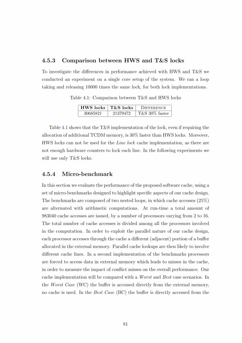
4.5.3 Comparison between HWS and T&S locks
To investigate the differences in performance achieved with HWS and T&S we
conducted an experiment on a single core setup of the system. We ran a loop
taking and releasing 10000 times the same lock, for both lock implementations.
Table 4.1: Comparison between T&S and HWS locks
HWS locks T&S locks Difference
30685821 21379472 T&S 30% faster
Table 4.1 shows that the T&S implementation of the lock, even if requiring the
allocation of additional TCDM memory, is 30% faster than HWS locks. Moreover,
HWS locks can not be used for the Line lock cache implementation, as there are
not enough hardware counters to lock each line. In the following experiments we
will use only T&S locks.
4.5.4 Micro-benchmark
In this section we evaluate the performance of the proposed software cache, using a
set of micro-benchmarks designed to highlight specific aspects of our cache design.
The benchmarks are composed of two nested loops, in which cache accesses (25%)
are alternated with arithmetic computations. At run-time a total amount of
983040 cache accesses are issued, by a number of processors varying from 2 to 16.
The total number of cache accesses is divided among all the processors involved
in the computation. In order to exploit the parallel nature of our cache design,
each processor accesses through the cache a different (adjacent) portion of a buffer
allocated in the external memory. Parallel cache lookups are then likely to involve
different cache lines. In a second implementation of the benchmarks processors
are forced to access data in external memory which leads to misses in the cache,
in order to measure the impact of conflict misses on the overall performance. Our
cache implementation will be compared with a Worst and Best case scenarios. In
the Worst Case (WC) the buffer is accessed directly from the external memory,
no cache is used. In the Best Case (BC) the buffer is directly accessed from the
81
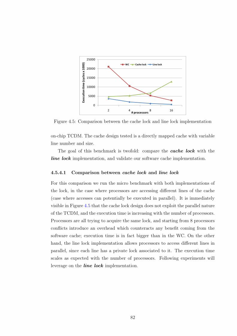
0
5000
10000
15000
20000
25000
2 4 8 16
Ex
ecu
o
n
me
(cy
cle
s x
10
00
)
# processors
WC Cache lock Line lock
Figure 4.5: Comparison between the cache lock and line lock implementation
on-chip TCDM. The cache design tested is a directly mapped cache with variable
line number and size.
The goal of this benchmark is twofold: compare the cache lock with the
line lock implementation, and validate our software cache implementation.
4.5.4.1 Comparison between cache lock and line lock
For this comparison we run the micro benchmark with both implementations of
the lock, in the case where processors are accessing different lines of the cache
(case where accesses can potentially be executed in parallel). It is immediately
visible in Figure 4.5 that the cache lock design does not exploit the parallel nature
of the TCDM, and the execution time is increasing with the number of processors.
Processors are all trying to acquire the same lock, and starting from 8 processors
conflicts introduce an overhead which counteracts any benefit coming from the
software cache; execution time is in fact bigger than in the WC. On the other
hand, the line lock implementation allows processors to access different lines in
parallel, since each line has a private lock associated to it. The execution time
scales as expected with the number of processors. Following experiments will
leverage on the line lock implementation.
82
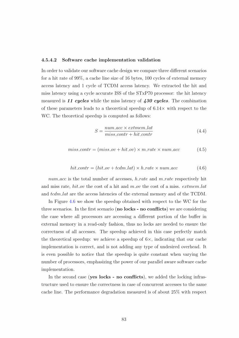
4.5.4.2 Software cache implementation validation
In order to validate our software cache design we compare three different scenarios
for a hit rate of 99%, a cache line size of 16 bytes, 100 cycles of external memory
access latency and 1 cycle of TCDM access latency. We extracted the hit and
miss latency using a cycle accurate ISS of the STxP70 processor: the hit latency
measured is 11 cycles while the miss latency of 430 cycles. The combination
of these parameters leads to a theoretical speedup of 6.14× with respect to the
WC. The theoretical speedup is computed as follows:
S =num acc× extmem lat
miss contr + hit contr(4.4)
miss contr = (miss ov + hit ov)×m rate× num acc (4.5)
hit contr = (hit ov + tcdm lat)× h rate× num acc (4.6)
num acc is the total number of accesses, h rate and m rate respectively hit
and miss rate, hit ov the cost of a hit and m ov the cost of a miss. extmem lat
and tcdm lat are the access latencies of the external memory and of the TCDM.
In Figure 4.6 we show the speedup obtained with respect to the WC for the
three scenarios. In the first scenario (no locks - no conflicts) we are considering
the case where all processors are accessing a different portion of the buffer in
external memory in a read-only fashion, thus no locks are needed to ensure the
correctness of all accesses. The speedup achieved in this case perfectly match
the theoretical speedup: we achieve a speedup of 6×, indicating that our cache
implementation is correct, and is not adding any type of undesired overhead. It
is even possible to notice that the speedup is quite constant when varying the
number of processors, emphasizing the power of our parallel aware software cache
implementation.
In the second case (yes locks - no conflicts), we added the locking infras-
tructure used to ensure the correctness in case of concurrent accesses to the same
cache line. The performance degradation measured is of about 25% with respect
83
to the previous case (no locks - no conflicts). The overhead measured is en-
tirely due to the extra code added in the lookup procedure, to handle the lock
of each line. To validate this assertion we have inspected the assembly code of
the innermost loop of the benchmark, and we found a 30% extra code executed
at each iteration. STxP70 processors are VLIW and issue instructions in bundle
of two. Our analysis has been conducted at the instruction bundle level. Given
the high hit rate considered (99%) we show in Figure 4.7 the assembly code of
the inner loop for a lookup&hit. In the case with locks, the compiler generates
14 instruction bundles with three memory read operations, making a total of 17
execution cycles (one cycle per bundle plus one extra cycle per memory access)
per iteration of the benchmark. For the case without locks the number of bun-
dles is 12 with only one memory read operation, for a total of 13 cycles. The
code in Figure 4.7, which is not highlighted, is not part of the cache code and is
introduced by the compiler. The compiler applies that kind of code reordering to
maximize the use of the double issue pipeline.
The last scenario presented in Figure 4.6 (Yes Locks - Yes Conflicts) is
aimed at measuring the overhead introduced by conflicts due to concurrent ac-
cesses to the same cache line by different processors. We consider a very negative
case with the 99% of conflict rate, meaning that almost all accesses to the software
cache lead to a conflict. Even in this case of high interference between processors
we can appreciate a remarkable speedup of 2.5×.
The second case discussed is likely to be the closest to a real application,
in which several processors are working on different subsets of the same data
structure. In that case the programmer will obtain a speedup of almost 5× with
respect to the worst case scenario. The same kind of analysis has been conducted
also for different values of the line size, showing similar results.
4.5.5 Object-Oriented extensions
To further explore the flexibility given by a software cache we designed a second
micro-benchmark in which the software cache is used as an object cache. A typical
scenario is a computer vision applications for object recognition, where descriptors
84
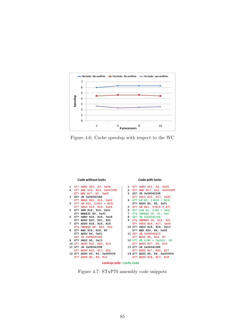
0
1
2
3
4
5
6
7
2 4 8 16
Sp
ee
du
p
# processors
No locks - No conflicts Yes locks - No conflicts Yes locks - yes conflicts
Figure 4.6: Cache speedup with respect to the WC
1 G7? SHRU R12, R4, 0x04
2 G7? AND R17, R12, 0x001FFF
3 G0? JR 0x5804C298
G7? SHLU R16, R17, 0x02
4 G7? LW R0, @(R16 + R23)
G7? ADDU R5, R5, 0x01
5 G7? LW R21, @(R16 + R7)
6 G7? LUB R1, @(R0 + 0x0)
7 G7& CMPEQU G0, R1, 0x0
8 G4? JR 0x5804C1D8
9 G7& CMPNEU G0, R12, R21
G7? SHLU R19, R17, 0x04
10 G7? SHLU R18, R18, 0x13
G7? AND R20, R4, 0x0F
11 G0? JR 0x5804C210
G7? ADDU R8, R16, R7
12 G7? SB @(R0 + 0x000), R9
G7? ADDU R17, R6, R19
13 G7? JR 0x5804C288
G7? ADDU R17, R20, R17
14 G7? ADDU R4, R4, 0x000004
G7? ADDU R18, R17, R18
1 G7? SHRU R23, R3, 0x04
2 G7? AND R16, R23, 0x001FFF
G7? AND R17, R3, 0x0F
3 G0? JR 0x5804C0A8
G7? SHLU R22, R16, 0x02
4 G7? LW R12, @(R21 + R22)
G7? SHLU R16, R16, 0x04
5 G7? SHR R18, R16, 0x01
G7? MAKE32 R0, 0x3C
6 G7? SHRU R18, R18, 0x1E
G7? ADDU R22, R21, R22
7 G7? ADDU R18, R16, R18
G7& CMPEQU G0, R23, R12
8 G7? AND R18, R18, R0
G7? ADDU R4, 0x01
G4? JR 0x5804C040
9 G7? SHLU R5, 0x13
10 G7? ADDU R12, R20, R16
11 G7? JR 0x5804C098
G7? ADDU R12, R17, R12
12 G7? ADDU R3, R3, 0x000004
G7? ADDU R5, R5, R12
Lookup code - Locks code
Code without locks Code with locks
Figure 4.7: STxP70 assembly code snippets
85
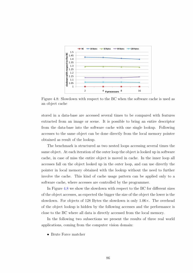
1
1.05
1.1
1.15
1.2
1.25
1.3
1.35
1.4
1.45
1.5
2 4 8 16
slo
do
wn
wit
h r
esp
ect
to
th
e B
C
# processors
BC 16 Bytes 32 Bytes 64 Bytes 128 Bytes
Figure 4.8: Slowdown with respect to the BC when the software cache is used asan object cache
stored in a data-base are accessed several times to be compared with features
extracted from an image or scene. It is possible to bring an entire descriptor
from the data-base into the software cache with one single lookup. Following
accesses to the same object can be done directly from the local memory pointer
obtained as result of the lookup.
The benchmark is structured as two nested loops accessing several times the
same object. At each iteration of the outer loop the object is looked up in software
cache, in case of miss the entire object is moved in cache. In the inner loop all
accesses fall on the object looked up in the outer loop, and can use directly the
pointer in local memory obtained with the lookup without the need to further
involve the cache. This kind of cache usage pattern can be applied only to a
software cache, where accesses are controlled by the programmer.
In Figure 4.8 we show the slowdown with respect to the BC for different sizes
of the object accesses, as expected the bigger the size of the object the lower is the
slowdown. For objects of 128 Bytes the slowdown is only 1.06×. The overhead
of the object lookup is hidden by the following accesses and the performance is
close to the BC where all data is directly accessed from the local memory.
In the following two subsections we present the results of three real world
applications, coming from the computer vision domain:
� Brute Force matcher
86
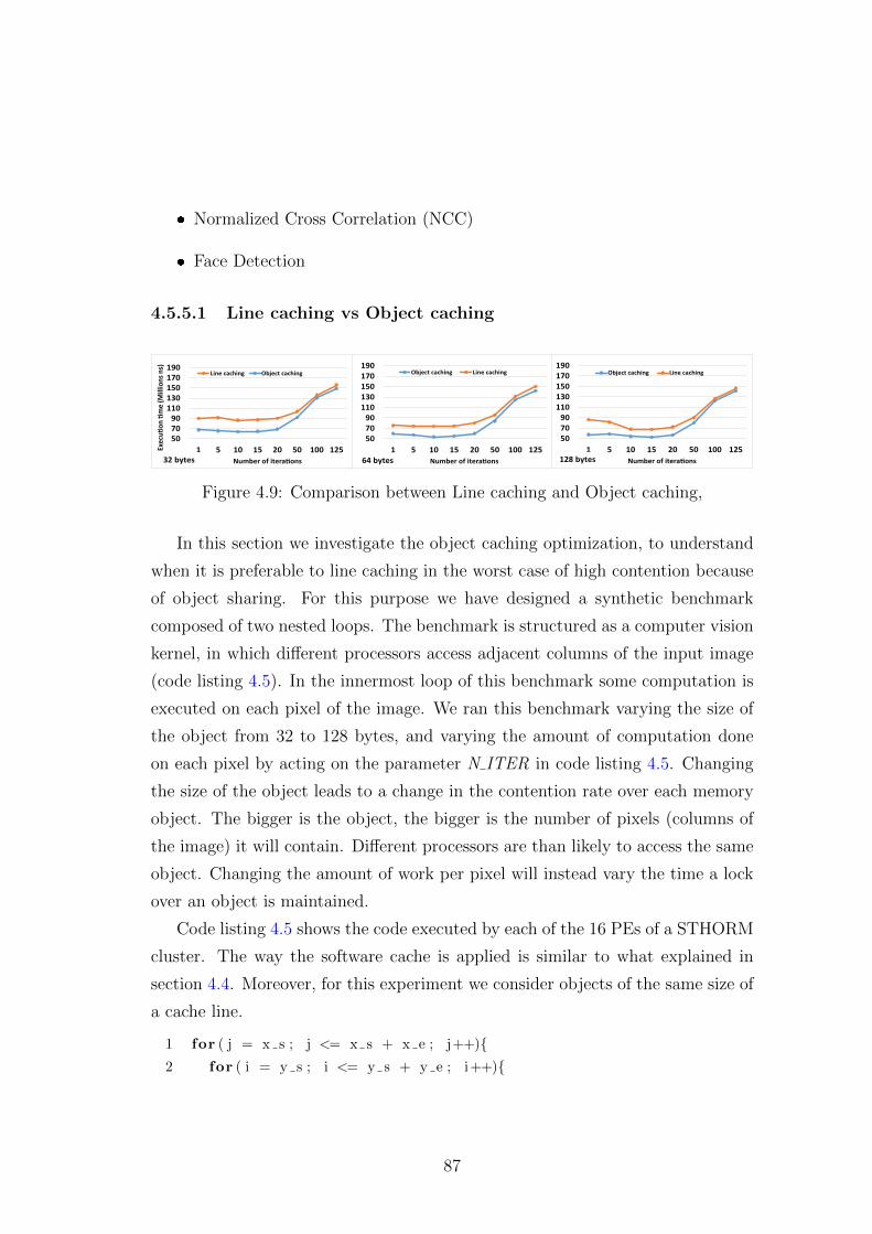
� Normalized Cross Correlation (NCC)
� Face Detection
4.5.5.1 Line caching vs Object caching
50
70
90
110
130
150
170
190
1 5 10 15 20 50 100 125
Number of itera!ons
Object caching Line caching
50
70
90
110
130
150
170
190
1 5 10 15 20 50 100 125
Number of itera!ons
Object caching Line caching
50
70
90
110
130
150
170
190
1 5 10 15 20 50 100 125Exe
cu!
on
!m
e (
Mil
lio
ns
ns)
Number of itera!ons
Line caching Object caching
32 bytes 64 bytes 128 bytes
Figure 4.9: Comparison between Line caching and Object caching,
In this section we investigate the object caching optimization, to understand
when it is preferable to line caching in the worst case of high contention because
of object sharing. For this purpose we have designed a synthetic benchmark
composed of two nested loops. The benchmark is structured as a computer vision
kernel, in which different processors access adjacent columns of the input image
(code listing 4.5). In the innermost loop of this benchmark some computation is
executed on each pixel of the image. We ran this benchmark varying the size of
the object from 32 to 128 bytes, and varying the amount of computation done
on each pixel by acting on the parameter N ITER in code listing 4.5. Changing
the size of the object leads to a change in the contention rate over each memory
object. The bigger is the object, the bigger is the number of pixels (columns of
the image) it will contain. Different processors are than likely to access the same
object. Changing the amount of work per pixel will instead vary the time a lock
over an object is maintained.
Code listing 4.5 shows the code executed by each of the 16 PEs of a STHORM
cluster. The way the software cache is applied is similar to what explained in
section 4.4. Moreover, for this experiment we consider objects of the same size of
a cache line.
1 for ( j = x s ; j <= x s + x e ; j++){2 for ( i = y s ; i <= y s + y e ; i++){
87
3 unsigned char p = in img [ f ( i , j ) ] ;
4
5 for ( int k = 0 ; k < N ITER ; k++){6 c += p * K;
7 c *= p * K;
8 c |= p * K;
9 }10 }11 }
Listing 4.5: Line caching vs Object caching synthetic benchmark
Figure 4.9 shows that when the computation done per pixel (or per object
element) is lower than 20 iterations, object caching has the best performance.
The performance improvement with respect to line caching is ∼ 40%. In this ex-
ample 6 arithmetic operations are executed at each iteration, thus object caching
performs the best below ∼ 120 − 150 arithmetic operations executed per object
element (byte in this case).
As expected, when increasing the number of iterations object caching suf-
fers the long critical section. What happens is that most of the processors are
blocked until the object becomes free again. Beyond the ∼ 120− 150 arithmetic
operations, the gain obtained with respect to line caching is in fact reduced to
∼ 4%. This effect is much more visible increasing the size of the object. With
objects of 128 bytes we see the maximum excursion, with the gain ranging from
a peak of ∼ 45% with 1 iteration, to 4% going beyond 20 iterations. This is an
expected behavior, as the contention over each object is further increased due to
an increase size of the object itself.
The case for objects of 128 bytes has an interesting behavior: increasing
the number of iterations improves the performance of line caching instead of
decreasing it. This is happening because the time needed to refill each line is
amortized by the work done for each lookup, in combination with a higher number
of cache hits. This is true until 20 iterations are reached, when the big amount
of code executed on each pixel dominates the whole execution time.
In general we can conclude that object caching is always preferable to line
88
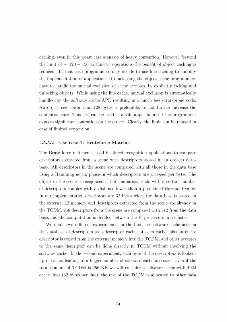
caching, even in this worst case scenario of heavy contention. However, beyond
the limit of ∼ 120 − 150 arithmetic operations the benefit of object caching is
reduced. In that case programmers may decide to use line caching to simplify
the implementation of applications. In fact using the object cache programmers
have to handle the mutual exclusion of cache accesses, by explicitly locking and
unlocking objects. While using the line cache, mutual exclusion is automatically
handled by the software cache API, resulting in a much less error-prone code.
An object size lower than 128 bytes is preferable, to not further increase the
contention rate. This size can be used as a safe upper bound if the programmer
expects significant contention on the object. Clearly, the limit can be relaxed in
case of limited contention.
4.5.5.2 Use case 1: Bruteforce Matcher
The Brute force matcher is used in object recognition applications to compare
descriptors extracted from a scene with descriptors stored in an objects data-
base. All descriptors in the scene are compared with all those in the data base
using a Hamming norm, phase in which descriptors are accessed per byte. The
object in the scene is recognized if the comparison ends with a certain number
of descriptors couples with a distance lower than a predefined threshold value.
In our implementation descriptors are 32 bytes wide, the data base is stored in
the external L3 memory and descriptors extracted from the scene are already in
the TCDM. 256 descriptors from the scene are compared with 512 from the data
base, and the computation is divided between the 16 processors in a cluster.
We made two different experiments: in the first the software cache acts on
the database of descriptors as a descriptor cache, at each cache miss an entire
descriptor is copied from the external memory into the TCDM, and other accesses
to the same descriptor can be done directly in TCDM without involving the
software cache. In the second experiment, each byte of the descriptors is looked-
up in cache, leading to a bigger number of software cache accesses. Even if the
total amount of TCDM is 256 KB we will consider a software cache with 1024
cache lines (32 bytes per line), the rest of the TCDM is allocated to other data
89
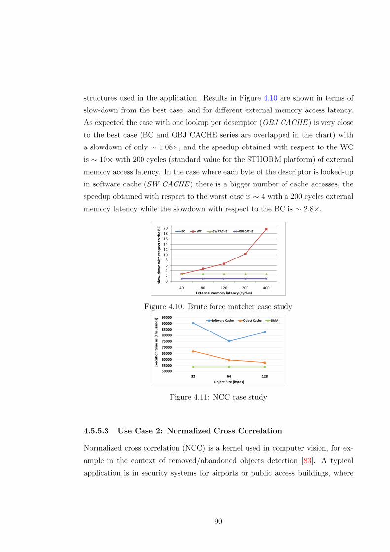
structures used in the application. Results in Figure 4.10 are shown in terms of
slow-down from the best case, and for different external memory access latency.
As expected the case with one lookup per descriptor (OBJ CACHE ) is very close
to the best case (BC and OBJ CACHE series are overlapped in the chart) with
a slowdown of only ∼ 1.08×, and the speedup obtained with respect to the WC
is ∼ 10× with 200 cycles (standard value for the STHORM platform) of external
memory access latency. In the case where each byte of the descriptor is looked-up
in software cache (SW CACHE ) there is a bigger number of cache accesses, the
speedup obtained with respect to the worst case is ∼ 4 with a 200 cycles external
memory latency while the slowdown with respect to the BC is ∼ 2.8×.
0
2
4
6
8
10
12
14
16
18
20
40 80 120 200 400
slo
w-d
ow
n w
ith
re
spe
ct t
o t
he
BC
External memory latency (cycles)
BC WC SW CACHE OBJ CACHE
Figure 4.10: Brute force matcher case study
50000
55000
60000
65000
70000
75000
80000
85000
90000
95000
32 64 128
Exe
cu
on
m
e n
s (T
ho
usa
nd
s)
Object Size (bytes)
So"ware Cache Object Cache DMA
Figure 4.11: NCC case study
4.5.5.3 Use Case 2: Normalized Cross Correlation
Normalized cross correlation (NCC) is a kernel used in computer vision, for ex-
ample in the context of removed/abandoned objects detection [83]. A typical
application is in security systems for airports or public access buildings, where
90
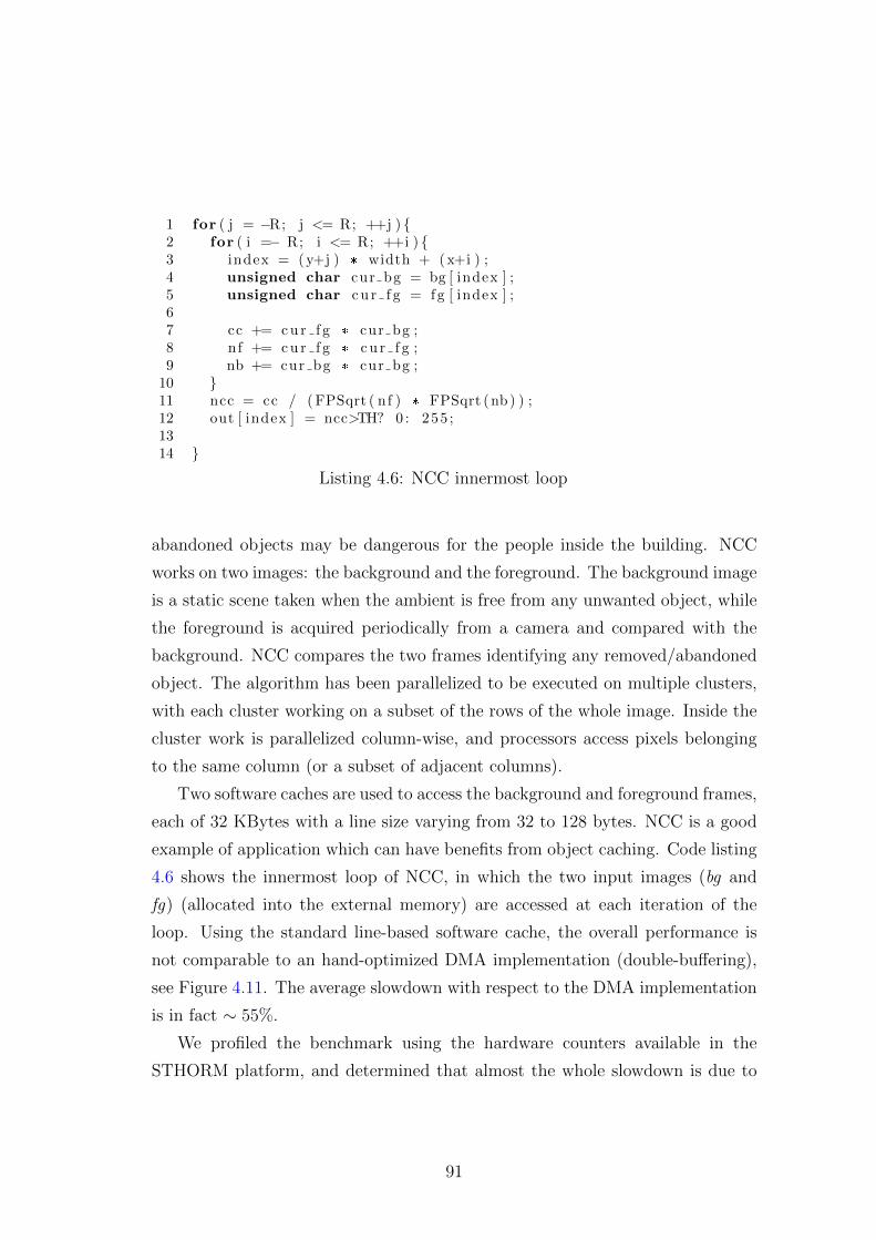
1 for ( j = −R; j <= R; ++j ) {2 for ( i =− R; i <= R; ++i ) {3 index = (y+j ) * width + (x+i ) ;4 unsigned char cur bg = bg [ index ] ;5 unsigned char cu r f g = fg [ index ] ;67 cc += cu r f g * cur bg ;8 nf += cu r f g * cu r f g ;9 nb += cur bg * cur bg ;
10 }11 ncc = cc / (FPSqrt ( nf ) * FPSqrt (nb) ) ;12 out [ index ] = ncc>TH? 0 : 255 ;1314 }
Listing 4.6: NCC innermost loop
abandoned objects may be dangerous for the people inside the building. NCC
works on two images: the background and the foreground. The background image
is a static scene taken when the ambient is free from any unwanted object, while
the foreground is acquired periodically from a camera and compared with the
background. NCC compares the two frames identifying any removed/abandoned
object. The algorithm has been parallelized to be executed on multiple clusters,
with each cluster working on a subset of the rows of the whole image. Inside the
cluster work is parallelized column-wise, and processors access pixels belonging
to the same column (or a subset of adjacent columns).
Two software caches are used to access the background and foreground frames,
each of 32 KBytes with a line size varying from 32 to 128 bytes. NCC is a good
example of application which can have benefits from object caching. Code listing
4.6 shows the innermost loop of NCC, in which the two input images (bg and
fg) (allocated into the external memory) are accessed at each iteration of the
loop. Using the standard line-based software cache, the overall performance is
not comparable to an hand-optimized DMA implementation (double-buffering),
see Figure 4.11. The average slowdown with respect to the DMA implementation
is in fact ∼ 55%.
We profiled the benchmark using the hardware counters available in the
STHORM platform, and determined that almost the whole slowdown is due to
91
Figure 4.12: Haar features used for Viola-Jones Face Detection
conflicts in the TCDM memory of each cluster. Conflicts are in turn due to the
high number of cache accesses (3727920 cache accesses). Profiling showed that
∼ 45% of the whole application execution time was spent in waiting for TCDM
conflicts. When object caching is used the total number of cache accesses is heav-
ily reduced (612612 cache accesses, ∼ 84% reduction), the percentage of TCDM
conflicts drops to ∼ 10%. The overall performance becomes only 10% lower than
the hand-optimized, explicit DMA-copy based implementation.
4.5.5.4 Use case 3: Face Detection
The Face Detection implementation taken into account for our experiments uses
the Viola-Jones algorithm [131]. The Viola-Jones face detection algorithm uses
on a cascade classifier that working on the integral image of the original picture,
is able to recognize if a subregion of an image contains a face or not. The cascade
classifier uses a set of features (Haar Features) which are shown in Figure 4.12,
which are applied to the image at each stage of the cascade. In our implementa-
tion of Face Detection processors in the same cluster work on different subregions
of the image applying the cascade classifier until a positive or negative result is
obtained.
We identified as a good candidate for software caching the cascade classifier.
The cascade is composed of an array of stages (21 in our example) with each
stage composed in turn by a number of features, and a stage threshold used to
decide whether the search should go to the next stage or if there is no face in the
current sub-region. Each stage of the cascade is an AdaBoost [51] classifier. Each
92
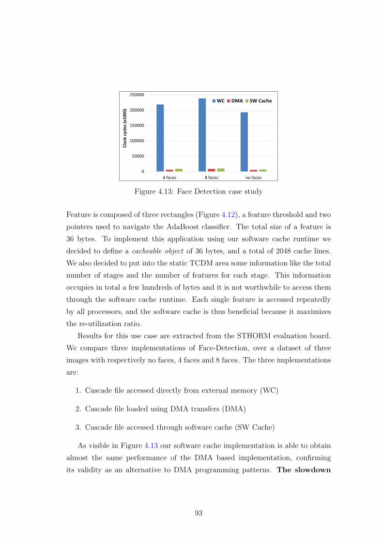
0
50000
100000
150000
200000
250000
4 faces 8 faces no faces
Clo
ck c
ycl
es
(x1
00
0)
WC DMA SW Cache
Figure 4.13: Face Detection case study
Feature is composed of three rectangles (Figure 4.12), a feature threshold and two
pointers used to navigate the AdaBoost classifier. The total size of a feature is
36 bytes. To implement this application using our software cache runtime we
decided to define a cacheable object of 36 bytes, and a total of 2048 cache lines.
We also decided to put into the static TCDM area some information like the total
number of stages and the number of features for each stage. This information
occupies in total a few hundreds of bytes and it is not worthwhile to access them
through the software cache runtime. Each single feature is accessed repeatedly
by all processors, and the software cache is thus beneficial because it maximizes
the re-utilization ratio.
Results for this use case are extracted from the STHORM evaluation board.
We compare three implementations of Face-Detection, over a dataset of three
images with respectively no faces, 4 faces and 8 faces. The three implementations
are:
1. Cascade file accessed directly from external memory (WC)
2. Cascade file loaded using DMA transfers (DMA)
3. Cascade file accessed through software cache (SW Cache)
As visible in Figure 4.13 our software cache implementation is able to obtain
almost the same performance of the DMA based implementation, confirming
its validity as an alternative to DMA programming patterns. The slowdown
93
between implementation 2 and 3 is in average 1.2×. Moreover this com-
parison confirms the validity of the arbitrary size object cache optimization. The
overall benefit of our software cache is visible when comparing implementation
1 with implementation 3, the average speedup obtained when using the
software cache is ∼ 25×. This speedup is due to a reduction of ∼ 60× in
the number of external memory access between the Worst Case and the software
cache version of the benchmark.
4.6 Conclusions
In this chapter we present a thread-safe implementation of software cache for
Scratchpad-Based multi-core Clusters. The proposed runtime implementation
has been developed for the STMicroelectronics STHORM fabric, by exploiting
several platform specific features. The main novelty of this work is the manage-
ment of concurrent access from different processors in a cluster. We have also
introduced an extension for Object Oriented software caching, to further speedup
applications working with multi-byte objects and minimize the global overhead
of the software cache. The Object Oriented extensions presented in this work can
also handle objects of arbitrary size, and have been designed to maintain a low
lookup overhead. Moreover we also provide a programming interface to help the
programmer in defining cacheable objects.
The object oriented optimization demonstrates to always perform better than
the line based implementation, with a best case of ∼ 40% improvement. How-
ever in case of high contention over objects, the benefit of object caching is small
(∼ 4%). In that case programmers may decide to use line caching to simplify the
implementation of applications. Using the object cache programmers have to ex-
plicitly handle the mutual exclusion, by explicitly locking and unlocking objects.
While using the line cache, mutual exclusion of cache accesses is automatically
handled by the software cache API, resulting in a much less error-prone code.
We have tested the software cache with three computer vision applications
namely: Bruteforce matcher, Face Detection and Normalized Cross Correlation.
94
Results obtained demonstrate that our software cache implementation introduces
a minimum overhead and can be used as an alternative to DMA programming,
with our software cache having a slowdown with respect to a DMA-based imple-
mentation of only 1.2× for Face Detection, and 1.1× for NCC. We measured
an overall speedup of ∼ 25×, and a heavy reduction in the number of external
memory accesses (60×). In this chapter we also demonstrate that the software
cache is a valid alternative to DMA programming. The slowdown with respect
to the DMA implementation of our benchmarks is acceptable, and is counterbal-
anced by a much more simple implementation of the applications when based on
the software cache.
In the future we plan to explore DMA based prefetching techniques, to min-
imize as much as possible the effects of cold misses. We also want to explore a
multi-cluster implementation of our runtime and cooperative caching schemes, to
fully exploit the TCDMs of all clusters in a STHORM fabric. Another evolution
is the automation of the software cache, exploiting the support of the compiler.
A possibility is to define a cacheable object data type qualifier, which the pro-
grammer can use to mark cacheable objects. The compiler will be then in charge
of inserting all the software cache calls needed to initialize, and actually access
objects from the cache.
Even if results of this chapter demonstrate that a Software Cache is an ef-
fective tool to decrease the programming effort, and ensure an almost optimal
exploitation of the hardware capabilities, it suffers from a major problem: it is
re-active. During the cache lookup, and especially in case of a cache miss, pro-
cessors are not allowed to perform any other task wasting precious clock-cycles.
In the next chapter, thanks to a DMA based pre-fetching mechanism, the needs
of processors are forecasted with the goal of reducing the average wait time for
each cache access (especially for cache misses).
95

96
Chapter 5
Memory Virtualization: DMA
assisted prefetching
5.1 Overview
Heterogeneous Multi-Processor Systems on a Chip (MPSoC) are a recent evolu-
tion in integrated computing platforms, where standard multi-core CPUs work
alongside with highly parallel and at the same time energy efficient programma-
ble acceleration fabrics [96] [107] [33]. Heterogeneous computing is motivated by
the desire to lower the complexity of manufacturing the chip, and to follow the
power consumption constraints imposed by the market. One example platform is
STHORM of STMicroelectronics [88]. STHORM is composed by several comput-
ing units, packed in groups of 16 (Cluster). Processors in the same cluster have
private I-Caches and share a multi-bank data scratchpad. The choice of having
a shared data scratchpad inside each cluster makes it possible to achieve higher
computational density (GOPS/mm2), as scratchpads are more area-efficient than
caches [20]. Data scratchpads, however, force the programmer to deal explicitly
with external-memory-to-scratchpad transfers. This is usually automatic, and
transparent to the programmer, when a hardware data cache is available. More-
over, the gap between processors architectures and memories is growing, with the
memory access latency being a plague for the performance of applications. Hiding
97
this latency is thus a key factor when programming applications, especially for
those with a high intensity of memory accesses.
A growing focus area for parallel memory-intensive applications is multimedia
and computer vision, where computation is split into chunks and data subsets are
repeatedly moved in and out from the external memory to the scratchpad. This
type of computation is often subject to real-time constraints. It is immediate
to understand how disruptive those external memory transfers can be, especially
if synchronous (wait for the transfer to complete), on the global performance of
an application. One well-known solution available today is overlapping memory
transfers with computation. Application are structured to work on a block of
data, while in the meantime the next block to be processed is being transferred
into local memory using a Direct Memory Access (DMA) engine. This technique
is called double-buffering.
DMA based programming with double-buffering has three main drawbacks: 1)
applications need to be heavily modified to use double-buffering. 2) the available
amount of local scratchpad can limit the effectiveness of the technique (two times
the size of a block is needed). 3) the programmer has to deal with the trade-off
between the size of the block to be transferred and the amount of computation
performed on it. If the amount of work performed on each data block is not well
chosen, it might not hide the transfer of the next data block.
An alternative to DMA programming which has always triggered interest are
software caches. However, even if software caches can lower the programming
complexity compared with DMA, they still have a major drawback: they are re-
active. A software cache reacts according to the result of the lookup, and in case
of miss a line refill is programmed. The completion of the transfer is waited before
the application can continue. Processors waiting for the refill of a particular line
can not perform any other task, wasting clock cycles. DMA-assisted prefetch-
ing can be used to anticipate the needs of processors by programming cache line
transfers ahead of time, with the aim of minimizing the possibility of waiting
for a certain datum. Software prefetching however is strongly dependent on the
memory access pattern of applications: those with a regular access pattern can
98
benefit from automatic prefetching techniques, prefetching cache lines according
to a fixed rule. On the other hand, for applications with a more irregular access
pattern, it is useful to exploit the hints of the programmer to know which line to
prefetch next.
In this work is evaluated the effectiveness of DMA-assisted prefetching, ap-
plied to a parallel software cache implementation [102] for the STHORM accel-
eration fabric. The basic idea is to use DMA-prefetching to further minimize
the number of blocking cache misses, and thus avoiding wait periods where pro-
cessors waste clock cycles. The goal of this work is thus to transform the
software cache in [102] into a pro-active entity. Both automatic and pro-
grammer assisted prefetching techniques have been evaluated when applied to
three computer vision case studies: Viola-Jones Face Detection [131], Normalized
Cross-Correlation (NCC) [83] and a color conversion algorithm. The overhead
due to software prefetching is also discussed in the experimental results section.
The rest of the chapter is organized as follows: in Section 5.2 we give an
overview of related work on data prefetching and software caches. Section 5.3
describes the prefetching techniques used in this work. Section 5.4 gives the
implementation details of our prefetching infrastructure. Finally in Sections 5.5
we show experimental results, and in Section 5.6 closing remarks and future work
are presented.
5.2 Related work
Data prefetching is not new to the research community, first works appeared in
the late 70s [117], and since then many works have been published. The need
for prefetching started with the beginning of processors performance boost which
at the end led to the multi-core era. Processors became faster and faster, while
memory hierarchies were not able to follow this trend. By using software prefetch-
ing it was possible to mitigate the effects of memory latency, and both hardware
[41, 43, 70, 79] and software [34, 94] solutions have been studied. Hardware
prefetching has the benefit of no extra code overhead, but the prefetch scheme
99
is locked to what the underlying hardware permits. On the contrary, software
based prefetching mechanisms allow to implement whatever prefetch one might
be interested in, at the price of extra code execution due to address calculation
and actual prefetch triggering. Both mechanisms of course are meant to solve
the same problem: reduce the number of cache misses and mitigate the memory
latency.
Also DMA engines have already been used for software prefetching; Authors
in [47] present a DMA-based prefetch system which prefetches arrays with a high
reuse rate, according to an analysis of the code aimed at minimizing energy and
maximizing performance. DMA priorities and queues are used to resolve possible
data dependencies between different iterations of the same kernel ensuring the
correctness of each memory access. Authors in [108] exploit the DMA engines
available in the Cell BE processor, to prefetch data in I/O intensive workloads.
Files are first read from the central core and then distributed to each SPE using
DMA transfers.
We concentrate our attention on Software Prefetching applied to Software
Caches for scratch-pad-based Clustered Multicore accelerators. Several works on
software caches can be found in literature, with those related to scratch-pad based
multicore mostly targeting the Cell BE processor. Examples are: [116], where
authors propose an alternative design aimed at reducing the miss rate. Authors in
[36] present a software cache based OpenMP runtime for the Cell BE processor,
leveraging the weak consistency model to ensure memory accesses correctness.
Finally authors in [102] present a parallel software cache implementation for the
STMicroelectronics STHORM acceleration fabric in which, differently from the
previously described related work, the software cache is shared among all proces-
sors in a cluster.
In this work we want to mix Software Caching and DMA-based prefetching
to further decrease the miss rate of the software cache runtime presented in [102],
with the aim of minimizing the stall of processors waiting for a line to be refilled.
Prefetching applied to software caches is not a new topic; Authors in [37] imple-
ment a prefetching mechanism for irregular memory references, to reduce the miss
100
rate of the software cache runtime provided with the Cell BE SSC Research Com-
piler. The approach is relying both on compiler support and run-time decisions.
Authors in [37] apply prefetching only to irregular memory references, while reg-
ular ones are resolved using direct-buffering. In our work we apply prefetching
to all memory accesses, tackling with the irregular one by using the programmer
assisted prefetching interface. In our approach regular references are still relying
on software cache and prefetching, because techniques like direct-buffering reduce
the amount of available local memory due to statically pre-allocated buffers.
5.3 Prefetch techniques
Even if a software cache can be used to heavily reduce the programming phase of
an application, when compared to hand optimized DMA-based programming, it
still suffers from one main limitation: a software cache is a reactive entity. When
a processor, during the lookup phase, gets a miss it has to program the refill of the
cache: victim selection, write back and finally the actual line refill. In this case
the software cache is reacting to the miss event. During the refill phase, however,
the requesting processor is stalled waiting for the new line to be copied in cache,
and finally access it. When waiting for the line refill to complete, regardless of
its implementation (DMA, explicit copies), processors are not allowed to perform
any other work, wasting clock cycles. As already stated, the best way to get the
full performance from a platform like STHORM is to hide as much as possible
the latency of external-memory-to-scratchpad transfers, with the DMA playing a
central role.
DMA-Assisted software prefetching is a good candidate to be used to
further reduce the wait time of processors. Using line prefetching it is possible
to anticipate the need of a processor, loading into the cache a line which will be
accessed in the near future. However, the effectiveness of prefetching is strongly
dependent from applications memory access pattern. Applications accessing the
memory with a regular (predictable) pattern are likely to benefit from automatic
prefetch mechanisms, prefetching cache lines with a fixed rule. While for applica-
101
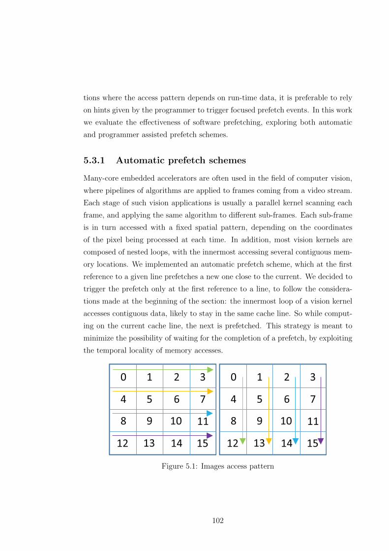
tions where the access pattern depends on run-time data, it is preferable to rely
on hints given by the programmer to trigger focused prefetch events. In this work
we evaluate the effectiveness of software prefetching, exploring both automatic
and programmer assisted prefetch schemes.
5.3.1 Automatic prefetch schemes
Many-core embedded accelerators are often used in the field of computer vision,
where pipelines of algorithms are applied to frames coming from a video stream.
Each stage of such vision applications is usually a parallel kernel scanning each
frame, and applying the same algorithm to different sub-frames. Each sub-frame
is in turn accessed with a fixed spatial pattern, depending on the coordinates
of the pixel being processed at each time. In addition, most vision kernels are
composed of nested loops, with the innermost accessing several contiguous mem-
ory locations. We implemented an automatic prefetch scheme, which at the first
reference to a given line prefetches a new one close to the current. We decided to
trigger the prefetch only at the first reference to a line, to follow the considera-
tions made at the beginning of the section: the innermost loop of a vision kernel
accesses contiguous data, likely to stay in the same cache line. So while comput-
ing on the current cache line, the next is prefetched. This strategy is meant to
minimize the possibility of waiting for the completion of a prefetch, by exploiting
the temporal locality of memory accesses.
0 1 2 3
4 5 6 7
8 9 10 11
12 13 14 15
0 1 2 3
4 5 6 7
8 9 10 11
12 13 14 15
Figure 5.1: Images access pattern
102
Computer vision kernels are likely to access software cache lines with a certain
spatial locality. Starting from the actual pixel coordinates, vision kernels usually
access adjacent pixels in the same image row or in adjacent rows. Figure 5.1 shows
in different colors different threads, and their possible image access pattern (im-
ages are divided into cache lines). Two different prefetching policies are defined,
called spatial prefetching policies. In the first policy the next adjacent line is
prefetched at the first reference to each line (horizontal-prefetching), while in
the second policy the cache line below (int the next row) the actual is prefetched
(vertical-prefetching). To enable automatic prefetching the lookup routine of
the software cache in [102] has been modified, and added few data structures
needed to manage lines prefetching.
5.3.2 Programmer assisted prefetch
As already stated, automatic prefetching may be less effective when the access
pattern of the application is not predictable, or does not follow the automatic
prefetch policy. We have then implemented two programmer-assisted prefetch
techniques, based on the following assumptions. Several vision applications access
memory buffers computing the address using runtime data. Automatic prefetch
may suffer of a non-predictable memory access pattern, we have then defined
an API which allows the programmer to manually trigger the prefetch of the
next line used by the application. The first programmer assisted prefetch API is
composed by the following function:
1 void p r e f e t c h l i n e ( void * ext mem address ,
cache parameters * cache ) ;
This function programs the prefetch of the cache line where the address
ext mem address is contained. The second parameter (cache) holds the pointer
to the data structure maintaining the whole software cache status. The comple-
tion of the DMA transfer triggered for each prefetch is checked only at the first
reference to the line.
103
The second manual prefetch interface can be used to avoid cold misses. Some
applications access data buffers starting from the first elements through its end,
examples are arrays or trees. Almost all applications have an initialization phase,
in which indexes and addresses needed to share the computation among multiple
processors are computed (prolog). It is possible to exploit the prolog of an ap-
plication to prefetch the content of the whole cache, or part of it, with the aim
of avoiding cold misses (initial cache prefetching). The programming API is
composed by two functions:
1 dma req t * p r e f e t c h c a c h e ( void * ext mem address ,
uint32 t from ) ;
2
3 void w a i t c a c h e p r e f e t c h (dma req t * dma events ) ;
The first function (prefetch cache) takes two input parameters:
ext mem address represents the address in global memory of the buffer to
prefetch, while from represents the starting offset in byte from which the prefetch
will start. We decided to put the from parameter, to give programmers the free-
dom to start the prefetch from the point in the data buffer they consider to
be the best (i.e. the computation starts accessing from there). The value re-
turned holds the pointer to the DMA event associated with the cache prefetch.
The second function (wait cache prefetch) is used to wait for the comple-
tion of the prefetch. The only input parameter is dma events, used to pro-
vide the DMA event pointer to wait for (returned by wait cache prefetch).
wait cache prefetch is usually placed just before the beginning of the portion
of the application using the software cache.
5.4 Prefetch infrastructure
In this section are described the modifications made to the software cache in [102],
to support both automatic and programmer assisted prefetch. The part mainly
involved by modifications is the lookup routine, but also some additional data
structures have been defined.
104
5.4.1 Additional data structures
Each prefetch event is associated to a DMA event generated by the DMA API
itself. A prefetch is usually triggered by a core while its completion is likely to
be verified by another one. To support the sharing of DMA events we defined a
common buffer of 16 events (events buf), making the assumption of a maximum
of one prefetch per core active at the same time.
The status of each cache line has been extended with two extra flags: the
PREFETCHING flag and the FIRST ACCESS flag. The former is used to check if a
line is prefetching, while the latter is used to check for the first access to a cache
line. The usage of the two flags is better explained later in this section. Due to the
need of the two new flags, also the dirty bit has been moved from the tag of the
line to a new line status field (1 byte). Each cache line has also a private memory
location, containing the index of the DMA event associated to its prefetch (1
byte). The index of the event is obtained when initializing the prefetch and is
computed using events buf as a circular buffer. The circular buffer uses a mutex
(T&S based), to avoid different processors accessing the DMA events buffer at
the same time.
To summarize, with respect to the original implementation we add: 2 bytes
per cache line, a buffer common to the entire cache composed by 16 DMA events
(32 bytes each), and an extra lock used to manage the DMA events buffer.
5.4.2 Lookup routine extension
The lookup routine has been modified in order to support line prefetch. Since the
prefetch system presented in this work is based only on software, it adds some
overhead to the original software cache implementation. Such overhead, only due
to the extra code, will be discussed in Section 6.6.
At each cache lookup it is first verified if the current line is already being
prefetched, by checking the PREFETCHING flag in the line status register. Proces-
sors trying to access a line which is already prefetching are forced to wait, until
the DMA transfer is completed. The DMA event to wait for can be easily found
105
using the private location associated to the line. Once the prefetch is finished,
the normal lookup phase is executed: check if the current access is a hit or a miss.
The final phase of the lookup checks if the line is being referenced for the
first time, and if this is the case the prefetch of a new line is programmed. We
decided to trigger the prefetch at the first reference to a cache line, to maximize
the possible overlap between the computation on the actual line and the prefetch
of the next one. The line to be prefetched is chosen according to the prefetch
policy being used.
5.4.3 Line prefetch subroutine
The line prefetch subroutine is in charge of applying the prefetch policy, according
to the line which is currently accessed or to the hint of the programmer. The first
important step performed in this phase is to identify the prefetch candidate, and
acquire the lock of the line in which it will be placed (prefetch victim, identified
according to the associativity policy of the software cache). This is necessary to
avoid overwriting a line which is being accessed by some other processor. Before
actually programming the DMA transfer a set of sanity checks is performed, to
understand whether the prefetch should be triggered or not:
1. The prefetch victim is in turn prefetching: If the victim selected to be sub-
stituted by the new line is in turn prefetching, the processor must wait for
the completion of the prefetch.
2. Presence in cache of the line to prefetch: If the line to be prefetched is al-
ready in cache, there is no need to prefetch it.
The two conditions may be overlapping (i.e. the line a processor wants to
prefetch is already prefetching), in that particular case the prefetch routine will
not modify at all the status of the software cache. This is likely to be true when
two or more processors try to prefetch the same line.
Once the lock is acquired and all sanity checks are passed, the actual prefetch
is triggered. The prefetch is essentially composed by three phases: 1) DMA
event index acquisition, 2) source and destination addresses calculation, 3) DMA
106
transfer programming. After the DMA transfer is programmed the index of the
DMA event is saved into the specific location associated with the line, making it
available to other processors. The first of the three phases accesses the circular
buffer event buf, to get the first free event slot. That phase requires the processor
to acquire a lock, before changing the status of the buffer.
Hit Miss Hit&prefetch Miss&prefetchNo prefetch 11/18 118/893 - -
Prefetch 21/46 - 127/197 215/1073
Table 5.1: Prefetch overhead added to the lookup function, each cell contains:#instructions / #clock cycles (line size 32 bytes)
5.5 Experimental Results
5.5.1 Experimental Setup
All our experiments have been performed on a real implementation of the
STHORM acceleration fabric in 28 nm CMOS. The evaluation board consists
of a Xilinx ZYNQ ZC-702 chip (Host) featuring a dual Core ARM Cortex A9,
mainly used to run the Android operating system and to submit tasks to the
STHORM fabric (using OpenCL). The STHORM chip is composed by four com-
puting clusters, each with 16 STxP70 processors, working at a clock frequency of
430 MHz, and a shared data scratchpad of 256 KBytes. The memory bandwith
towards the external memory is ∼ 300 MB/sec. The bandwidth is limited by a
slow link between STHORM and the host system, implemented on the FPGA
inside the ZYNQ chip.
All the benchmarks are implemented in OpenCL. The OpenCL runtime used
is part of the STHORM SDK provided together with the evaluation board. The
software cache and all prefetching extensions are implemented in standard C code,
which is compiled and linked as an external library to the application. Results
are presented in terms of execution time (nano seconds) or clock cycles, the latter
are extracted using the hardware counters available in the STHORM chip.
107
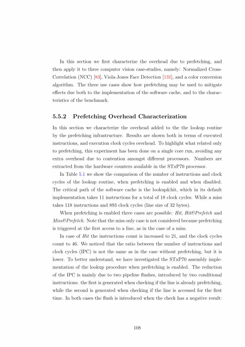
In this section we first characterize the overhead due to prefetching, and
then apply it to three computer vision case-studies, namely: Normalized Cross-
Correlation (NCC) [83], Viola-Jones Face Detection [131], and a color conversion
algorithm. The three use cases show how prefetching may be used to mitigate
effects due both to the implementation of the software cache, and to the charac-
teristics of the benchmark.
5.5.2 Prefetching Overhead Characterization
In this section we characterize the overhead added to the the lookup routine
by the prefetching infrastructure. Results are shown both in terms of executed
instructions, and execution clock cycles overhead. To highlight what related only
to prefetching, this experiment has been done on a single core run, avoiding any
extra overhead due to contention amongst different processors. Numbers are
extracted from the hardware counters available in the STxP70 processor.
In Table 5.1 we show the comparison of the number of instructions and clock
cycles of the lookup routine, when prefetching is enabled and when disabled.
The critical path of the software cache is the lookup&hit, which in its default
implementation takes 11 instructions for a total of 18 clock cycles. While a miss
takes 118 instructions and 893 clock cycles (line size of 32 bytes).
When prefetching is enabled three cases are possible: Hit, Hit&Prefetch and
Miss&Prefetch. Note that the miss only case is not considered because prefetching
is triggered at the first access to a line, as in the case of a miss.
In case of Hit the instructions count is increased to 21, and the clock cycles
count to 46. We noticed that the ratio between the number of instructions and
clock cycles (IPC) is not the same as in the case without prefetching, but it is
lower. To better understand, we have investigated the STxP70 assembly imple-
mentation of the lookup procedure when prefetching is enabled. The reduction
of the IPC is mainly due to two pipeline flushes, introduced by two conditional
instructions: the first is generated when checking if the line is already prefetching,
while the second is generated when checking if the line is accessed for the first
time. In both cases the flush is introduced when the check has a negative result:
108
line not prefetching or not first access. In case of Hit both conditions evaluate
false, and the two pipeline flushes take place. The two conditional constructs are
part of the prefetch infrastructure, and are generated by the STxP70 C compiler.
The Hit&Prefetch case is verified in case of hit and first access to the line.
In this case the instruction count is 127, and the clock cycles spent are 197. Here
it is possible to understand the effectiveness of prefetching: when prefetching, in
fact, the instruction count of a hit (127 instructions) is close to the one in case of
cache miss without prefetching (118 instructions). The main difference is in the
number of clock cycles: in the former case the clock cycles count is much lower,
197 clock cycles, against the 893 of the blocking cache miss case. The prefetch
of a cache line triggers an asynchronous DMA transfer, which overlaps with the
execution of the processor. The first access to the prefetched line will be a
hit, with the requesting processor saving ∼ 700 clock cycles. The saved
cycles would be otherwise spent in waiting for the line refill.
The last case is the Miss&prefetch, in which the instruction count is increased
to 215 with 1073 clock cycles spent in total. This case is the one which is less
suffering the code increase overhead, because the miss handling routine is already
composed by several instructions.
5.5.3 Case study 1: Normalized Cross Correlation
Normalized cross correlation (NCC) is a kernel used in computer vision, in the
context of video surveillance [83] [82]. A typical application is in security systems
for airports or public access buildings, where abandoned objects may be dangerous
for the people inside the building. NCC works on two images: the background and
the foreground. The background image is a static scene, taken when the ambient
is free from any unwanted object. The foreground is acquired periodically from
a camera, and compared with the background. NCC compares the two frames
identifying any removed/abandoned object. The algorithm has been parallelized
to be executed on multiple clusters, with each cluster working on a subset of the
rows of the whole image. Inside each cluster the work is parallelized again in a
column wise way, where processors access pixels belonging to the same column (or
109
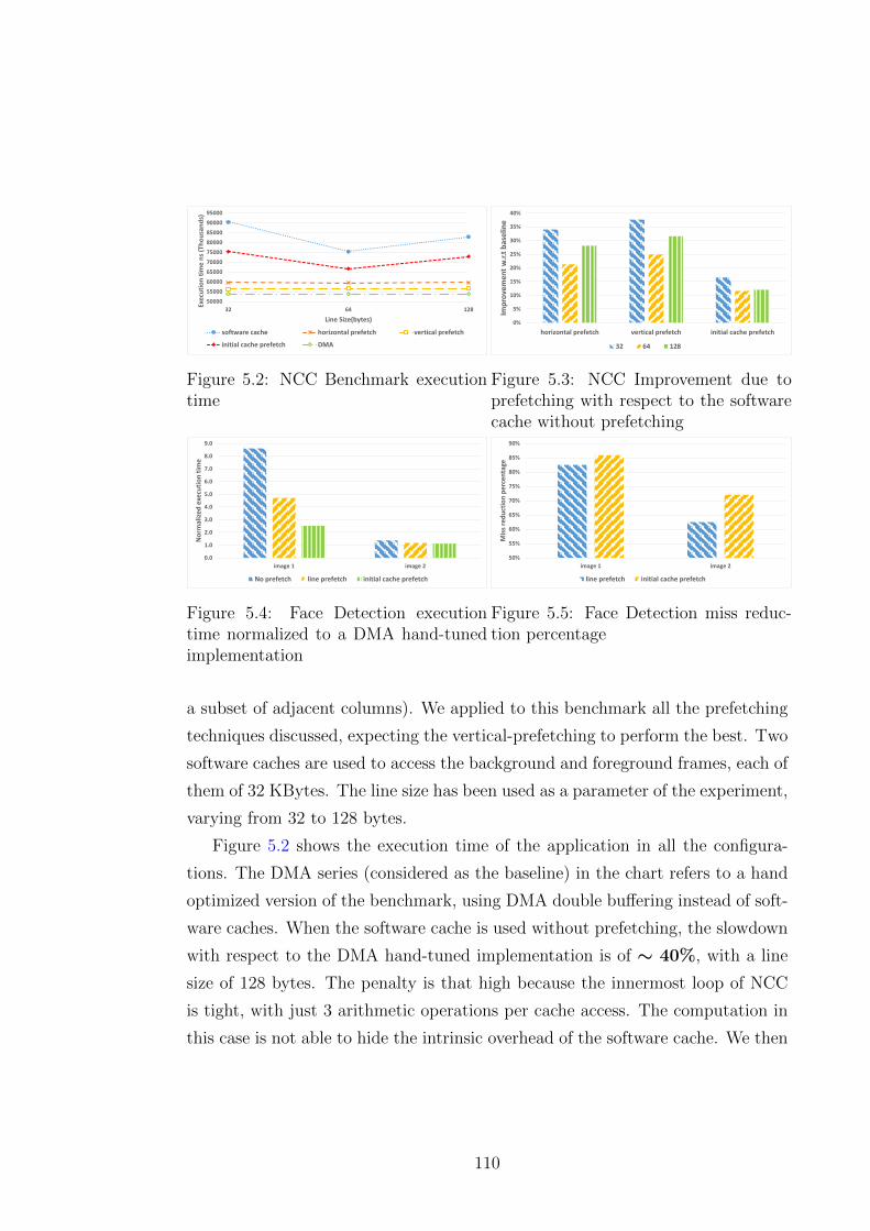
50000
55000
60000
65000
70000
75000
80000
85000
90000
95000
32 64 128
Exe
cuti
on
tim
e n
s (T
ho
usa
nd
s)
Line Size(bytes)
software cache horizontal prefetch vertical prefetch
initial cache prefetch DMA
Figure 5.2: NCC Benchmark executiontime
0%
5%
10%
15%
20%
25%
30%
35%
40%
horizontal prefetch vertical prefetch initial cache prefetch
Imp
rove
men
t w
.r.t
bas
elin
e
32 64 128
Figure 5.3: NCC Improvement due toprefetching with respect to the softwarecache without prefetching
0.0
1.0
2.0
3.0
4.0
5.0
6.0
7.0
8.0
9.0
image 1 image 2
No
rmal
ize
d e
xecu
tio
n t
ime
No prefetch line prefetch initial cache prefetch
Figure 5.4: Face Detection executiontime normalized to a DMA hand-tunedimplementation
50%
55%
60%
65%
70%
75%
80%
85%
90%
image 1 image 2
Mis
s re
du
ctio
n p
erc
en
tage
line prefetch initial cache prefetch
Figure 5.5: Face Detection miss reduc-tion percentage
a subset of adjacent columns). We applied to this benchmark all the prefetching
techniques discussed, expecting the vertical-prefetching to perform the best. Two
software caches are used to access the background and foreground frames, each of
them of 32 KBytes. The line size has been used as a parameter of the experiment,
varying from 32 to 128 bytes.
Figure 5.2 shows the execution time of the application in all the configura-
tions. The DMA series (considered as the baseline) in the chart refers to a hand
optimized version of the benchmark, using DMA double buffering instead of soft-
ware caches. When the software cache is used without prefetching, the slowdown
with respect to the DMA hand-tuned implementation is of ∼ 40%, with a line
size of 128 bytes. The penalty is that high because the innermost loop of NCC
is tight, with just 3 arithmetic operations per cache access. The computation in
this case is not able to hide the intrinsic overhead of the software cache. We then
110
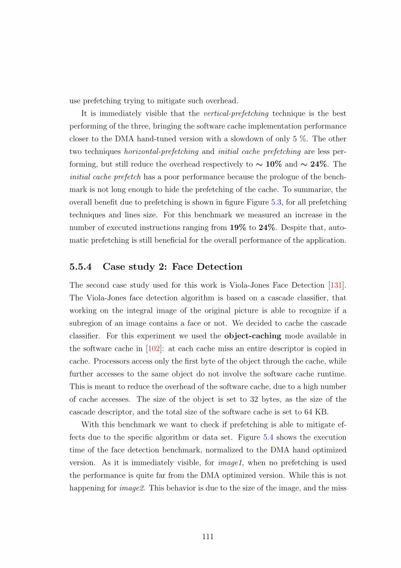
use prefetching trying to mitigate such overhead.
It is immediately visible that the vertical-prefetching technique is the best
performing of the three, bringing the software cache implementation performance
closer to the DMA hand-tuned version with a slowdown of only 5 %. The other
two techniques horizontal-prefetching and initial cache prefetching are less per-
forming, but still reduce the overhead respectively to ∼ 10% and ∼ 24%. The
initial cache prefetch has a poor performance because the prologue of the bench-
mark is not long enough to hide the prefetching of the cache. To summarize, the
overall benefit due to prefetching is shown in figure Figure 5.3, for all prefetching
techniques and lines size. For this benchmark we measured an increase in the
number of executed instructions ranging from 19% to 24%. Despite that, auto-
matic prefetching is still beneficial for the overall performance of the application.
5.5.4 Case study 2: Face Detection
The second case study used for this work is Viola-Jones Face Detection [131].
The Viola-Jones face detection algorithm is based on a cascade classifier, that
working on the integral image of the original picture is able to recognize if a
subregion of an image contains a face or not. We decided to cache the cascade
classifier. For this experiment we used the object-caching mode available in
the software cache in [102]: at each cache miss an entire descriptor is copied in
cache. Processors access only the first byte of the object through the cache, while
further accesses to the same object do not involve the software cache runtime.
This is meant to reduce the overhead of the software cache, due to a high number
of cache accesses. The size of the object is set to 32 bytes, as the size of the
cascade descriptor, and the total size of the software cache is set to 64 KB.
With this benchmark we want to check if prefetching is able to mitigate ef-
fects due to the specific algorithm or data set. Figure 5.4 shows the execution
time of the face detection benchmark, normalized to the DMA hand optimized
version. As it is immediately visible, for image1, when no prefetching is used
the performance is quite far from the DMA optimized version. While this is not
happening for image2. This behavior is due to the size of the image, and the miss
111
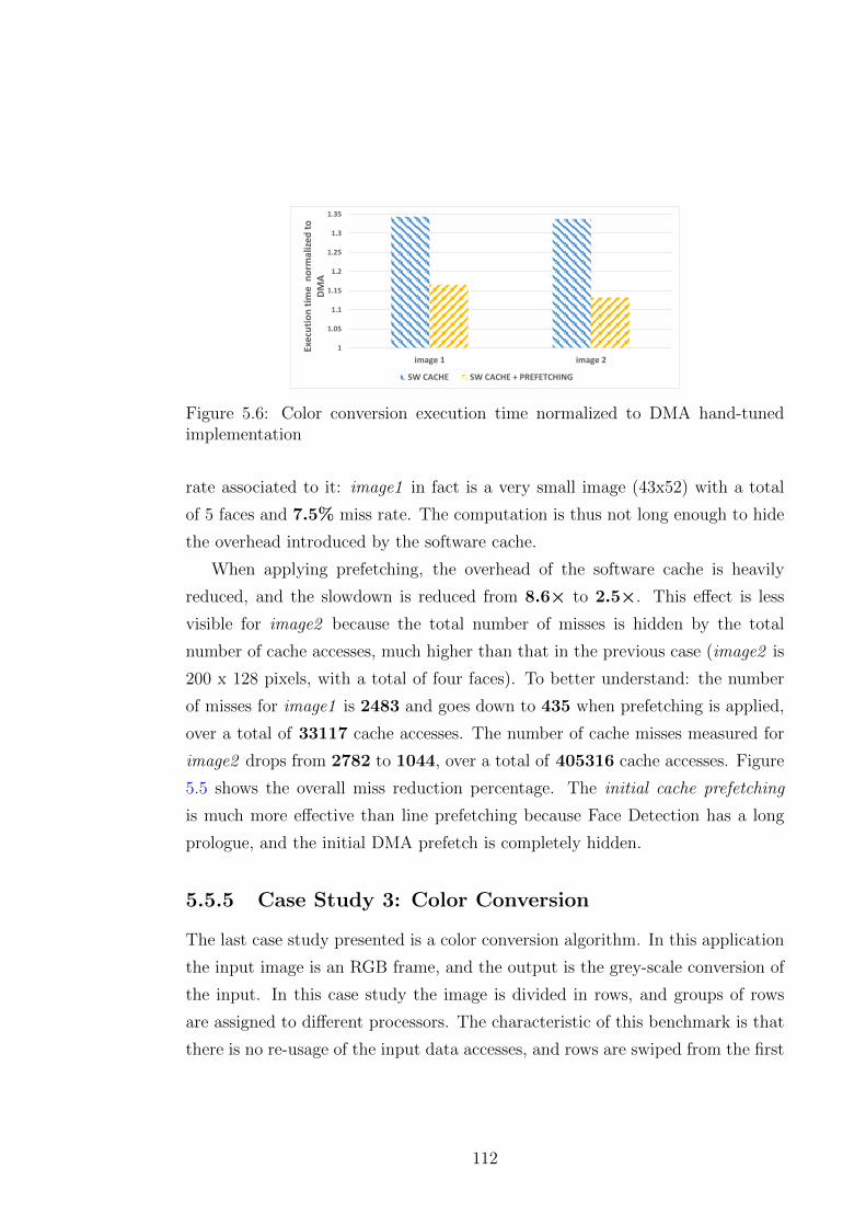
1
1.05
1.1
1.15
1.2
1.25
1.3
1.35
image 1 image 2
Exe
cuti
on
tim
e n
orm
aliz
ed
to
D
MA
SW CACHE SW CACHE + PREFETCHING
Figure 5.6: Color conversion execution time normalized to DMA hand-tunedimplementation
rate associated to it: image1 in fact is a very small image (43x52) with a total
of 5 faces and 7.5% miss rate. The computation is thus not long enough to hide
the overhead introduced by the software cache.
When applying prefetching, the overhead of the software cache is heavily
reduced, and the slowdown is reduced from 8.6× to 2.5×. This effect is less
visible for image2 because the total number of misses is hidden by the total
number of cache accesses, much higher than that in the previous case (image2 is
200 x 128 pixels, with a total of four faces). To better understand: the number
of misses for image1 is 2483 and goes down to 435 when prefetching is applied,
over a total of 33117 cache accesses. The number of cache misses measured for
image2 drops from 2782 to 1044, over a total of 405316 cache accesses. Figure
5.5 shows the overall miss reduction percentage. The initial cache prefetching
is much more effective than line prefetching because Face Detection has a long
prologue, and the initial DMA prefetch is completely hidden.
5.5.5 Case Study 3: Color Conversion
The last case study presented is a color conversion algorithm. In this application
the input image is an RGB frame, and the output is the grey-scale conversion of
the input. In this case study the image is divided in rows, and groups of rows
are assigned to different processors. The characteristic of this benchmark is that
there is no re-usage of the input data accesses, and rows are swiped from the first
112
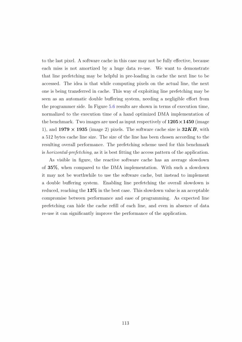
to the last pixel. A software cache in this case may not be fully effective, because
each miss is not amortized by a huge data re-use. We want to demonstrate
that line prefetching may be helpful in pre-loading in cache the next line to be
accessed. The idea is that while computing pixels on the actual line, the next
one is being transferred in cache. This way of exploiting line prefetching may be
seen as an automatic double buffering system, needing a negligible effort from
the programmer side. In Figure 5.6 results are shown in terms of execution time,
normalized to the execution time of a hand optimized DMA implementation of
the benchmark. Two images are used as input respectively of 1205×1450 (image
1), and 1979 × 1935 (image 2) pixels. The software cache size is 32KB, with
a 512 bytes cache line size. The size of the line has been chosen according to the
resulting overall performance. The prefetching scheme used for this benchmark
is horizontal-prefetching, as it is best fitting the access pattern of the application.
As visible in figure, the reactive software cache has an average slowdown
of 35%, when compared to the DMA implementation. With such a slowdown
it may not be worthwhile to use the software cache, but instead to implement
a double buffering system. Enabling line prefetching the overall slowdown is
reduced, reaching the 13% in the best case. This slowdown value is an acceptable
compromise between performance and ease of programming. As expected line
prefetching can hide the cache refill of each line, and even in absence of data
re-use it can significantly improve the performance of the application.
113
5.6 Conclusions
In this work we made a preliminary evaluation of DMA-assisted prefetching,
applied to a software-cache for scratch-pad based multi-core acceleration fabrics
[102]. The aim of the work is to evaluate whether prefetching can be beneficial
in further improving the software cache runtime. Not all applications will benefit
from automatic prefetching, we have thus presented a set of programmer-assisted
prefetching techniques. The schemes presented have been designed taking into
account the typical memory access pattern of computer vision applications, in
which spatial locality of accesses is often present and should be exploited. With
our experimental results we tried to understand if prefetching is able to mitigate
effects due to both the software cache runtime itself, or the application/dataset.
Results show that prefetching is a promising optimization, which allowed us to
finely optimize our benchmarks to reach a performance very close to the DMA
hand optimized version. This is the case of NCC, where the overall slowdown with
respect to the hand-tuned version is only 4%. The second benchmark instead
allowed us to see that even in case of non conventional datasets (image1, small
image and high miss rate), prefetching can heavily reduce the overhead of the
software cache speeding-up the execution of ∼ 3, 5×. With a global reduction
in the number of cache misses up-to 86%. In the last case study presented
(color conversion), we prove that prefetching may be useful even in cases where
software caching is less powerful (e.g. for applications with a low data re-usage
rate). The overall slowdown is reduced to the 13% in the best case. Prefetching
demonstrates to be a powerful optimization even in the context of software caches,
and should be studied more in detail. Possible future optimizations focus on
compiler assistance, to automate the usage of prefetch even in case of irregular
memory access patterns.
114
In the next chapter the focus will be moved to virtualization at its higher level
of abstraction, presenting a virtualization framework for many-core embedded
accelerators in Linux/KVM environments. The framework allows the usage of the
accelerator from different virtual machines, enhanced by an automatic memory
sharing mechanism.
115

116
Chapter 6
Many-Core accelerators
virtualization in Linux/KVM
environments
6.1 Overview
Modern embedded systems are increasingly taking on characteristics of general-
purpose systems. The ever-increasing demand for computational power has led to
the advent of sophisticated on-chip systems (SoC) composed of multi-core proces-
sors with complex multi-level coherent cache hierarchies, and capable of running
full-fledged operating systems supporting powerful abstractions such as virtual
memory. To further increase peak performance/watt, such powerful multicore
processors are being increasingly coupled to manycore accelerators composed of
several tens of simple processors, where critical computation kernels of an appli-
cation can be offloaded [8, 88, 124, 134].
On one hand, the new challenges posed by such sophisticated SoCs increas-
ingly make the case for embedded system virtualization [64]. Indeed, along with
the functionality of these system, the amount and complexity of their software
is also growing. Increasingly, embedded systems run both applications origi-
nally developed for the PC world and new applications written by program-
117
mers without embedded-systems expertise. This creates a demand for high-level
application-oriented operating systems (OS) with commodity APIs and easy-to-
use programming abstractions for the exploitation of manycore accelerators. At
the same time even modern high-end embedded systems still exhibit some sort of
real-time requirements, for which a different type of OS services is required (real-
time operating systems). The co-existence of different OSes must be supported
in full isolated domains for the obvious security issues. Furthermore, a strong
trend towards openness is typical of such systems, where device owners want to
download their own applications at any time. This again requires open APIs and
introduces all the security challenges known from the PC world.
On the other hand, the recent advent of manycores as co-processors to the
“host” system has generated the necessity for solutions to simplify application
development and to extend virtualization support to these accelerators. In the
near future it will be common to have multiple applications – possibly running on
distinct virtual machines on the host – concurrently offloading some computation
to the manycore accelerator. The importance of manycore virtualization and
programmability is witnessed by initiatives such as the Heterogeneous System
Architecture foundation [69], a non-profit consortium of major industrial and
academic players aimed at defining standard practices for heterogeneous SoC
platforms and associated programming models.
The main difficulty in traditional accelerator programming stems from a
widely adopted partitioned memory model. The host application creates data
buffers in main DRAM, and manages it transparently through coherent caches
and virtual memory. The accelerator features local, private memory, physically
addressed. An offload sequence to the accelerator requires explicit data manage-
ment, which includes i) programming system DMAs (capable of handling virtual
memory pointers) to copy data to the accelerator and ii) manually maintaining
consistency of data copies (host and accelerator side) with explicit coherency op-
erations (e.g., cache flushes). According to HSA, key to simplifying application
development for future heterogeneous SoCs is (coherent) shared-memory commu-
nication between the host and the manycore.
118
The HSA memory architecture moves management of host and accelerator
memory coherency from the developer’s hands down to the hardware. This al-
lows both the processors to access system memory directly, eliminating the need
to copy data to the accelerator (typically required in GPU programming), an
operation that adds significant latency and can wipe out any gains in perfor-
mance from accelerator parallel processing. This requires the accelerator to be
able to handle addresses in paged virtual memory, and is – in the HSA proposal –
achieved through dedicated HW support. The key hardware block to support co-
herent virtual memory sharing is the I/O Memory Management Unit (IOMMU),
responsible for translating virtual addresses into physical ones on the accelera-
tor side, and from protecting memory from illegal accesses issued therein. The
IOMMU is placed at the boundaries of the accelerator, and manages all transac-
tions towards the main memory, exchanging specific signals with the host MMU
to maintain a coherent view of the page tables.
The HSA roadmap is clearly defined, but as of yet there is no clear view about
practical implementation aspects and performance implications, particularly for
embedded SoCs. Currently, the first and only product compliant to the HSA
specification is the AMD Kaveri [9, 10], released early in 2014. The manycore
accelerator here is a powerful high-end GPU, with a number of processing clusters
each containing several data-parallel cores. The latter can be seen in fact as a
collection of SIMD ALUs sharing fetch/decode unit (and thus meant to operate
in lock-step mode), high-bandwidth interconnection towards local memory and
address translation logic. Focusing on embedded heterogeneous SoCs, a num-
ber of manycores has been recently proposed which, unlike GPUs, is based on
independent RISC cores [8, 124]. Clearly the area and energy budget for em-
bedded manycores is very different from that of high-end GPUs, which makes it
unaffordable to consider identical HW support for virtual memory coherency. In
particular, independent RISC cores would require independent MMU blocks for
proper address translation. Evidently, replicating a MMU block for every core in
an embedded manycore design is prohibitively costly.
While the road towards HSA-compliant embedded manycores is still unclear,
119
it is obvious the importance of simplifying accelerator programming and host-to-
accelerator communication in this domain. In absence of HW support, it is very
relevant to explore SW-only manycore virtualization support under the abstrac-
tion of a shared memory. In this chapter we present a software framework, based
on Linux-KVM, to allow shared-memory communication between host and many-
core and to provide manycore virtualization among several virtual machines. We
build upon the capability of the manycore to access the main DRAM memory
using physical, contiguous addressing to provide a software layer in charge of
transparently copying data into a memory area which is not subject to virtual
memory paging. This software layer implements a full-virtualization solution,
where unmodified guest operating systems run on virtual machines with the il-
lusion of being the only owners of the manycore accelerator. We implement a
prototype of the proposed solution for the STMicroelectronics STHORM board
[88], and we present a thorough characterization of its cost.
The rest of the chapter is organized as follows: in section 6.3 the many-
core accelerator target architecture is presented, and in section 6.4 the topic of
many-core accelerators virtualization is discussed. In section 6.5 we present the
virtualization framework, including our software-based solution to the memory
sharing problem. Finally in section 6.6 we assess the cost of the virtualization
, using a set of micro-benchmarks aimed at measuring the overhead of memory
copies. The virtualization infrastructure is also validated with a set of real world
case studies. In section 6.7 final remarks and future work are discussed.
6.2 Related work
Virtualization has been used for several years in the server and desktop computers
domain. Over the past few years the increase in complexity of embedded systems
has lured hardware manufacturers to designing virtualization ready devices [74,
132]. The main example is the introduction of hardware support for virtualization
in ARM processors, started with the ARMv7-A ISA [14]. This allowed existing
virtualization techniques, like the Linux Kernel Virtual Machine monitor (KVM)
120
[74] to be ported to ARM devices. More recently, the attention has shifted beyond
the processor onto other system I/O devices. ARM was among the first to propose
a set of extensions for system interconnections and to bring memory management
units and virtualization at the system level [15], enabling the sharing of I/O
resources between virtual machines.
General-Purpose GPU computing has started a trend, now embraced in both
desktop and embedded systems, to adopt manycore accelerators for the execution
of highly parallel, computation-intensive workloads. This kind of architectural
heterogeneity provides huge performance/watt improvements, but comes at the
cost of increased programming complexity and poses new challenges to existing
virtualization solutions. Those challenges have been explored to some extent in
the desktop/server domain. Becchi et al. [22] developed a software runtime for
GPU sharing among different processes on distributed machines, allowing the
GPU to access the virtual memory of the system. Ravi et al. [111] studied a
technique to share GPGPUs among different virtual machines in cloud environ-
ments.
Virtualization of embedded manycores is still in its infancy. The HSA Foun-
dation [69] aims at defining an architectural template and programming model
for heterogeneous embedded systems, where all the devices share the very same
memory map. However, the HSA specifications describe the system semantics,
while the physical implementation is up to the chip maker. Currently, no clear
solution to the coherent virtual memory sharing problem exists in the embed-
ded domain. AMD has recently released the first HSA-compliant APU, Kaveri
[10]. No details about the device implementation, nor performance figures are
currently available. ARM has a more modular approach to building a coherent
shared memory heterogeneous embedded system. Its CoreLink [1] technology
provides chip designers with the blocks to enable virtual memory at the system
level. These blocks include a virtualization ready interconnect (CCI-440) and a
virtualization ready System Memory Management Unit (MMU-400). However,
a SMMU (IOMMU) alone is not sufficient for virtualization of manycores like
those targeted in this chapter. Such manycores feature internal memory hierar-
121
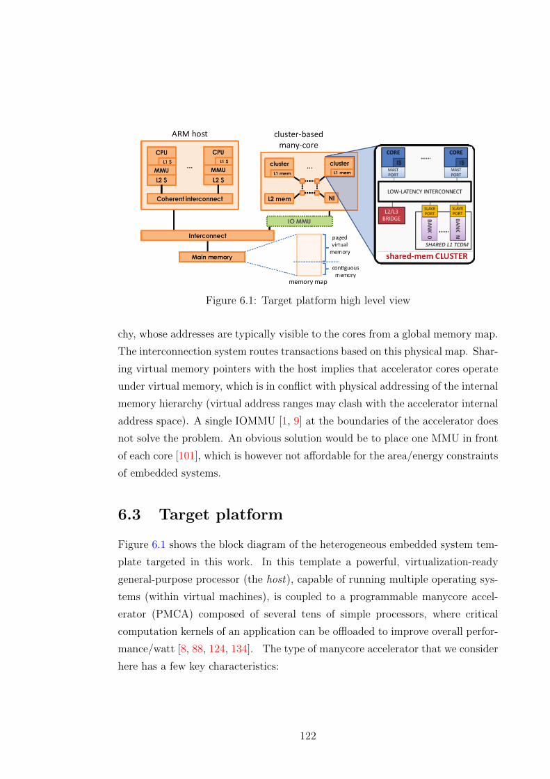
Figure 6.1: Target platform high level view
chy, whose addresses are typically visible to the cores from a global memory map.
The interconnection system routes transactions based on this physical map. Shar-
ing virtual memory pointers with the host implies that accelerator cores operate
under virtual memory, which is in conflict with physical addressing of the internal
memory hierarchy (virtual address ranges may clash with the accelerator internal
address space). A single IOMMU [1, 9] at the boundaries of the accelerator does
not solve the problem. An obvious solution would be to place one MMU in front
of each core [101], which is however not affordable for the area/energy constraints
of embedded systems.
6.3 Target platform
Figure 6.1 shows the block diagram of the heterogeneous embedded system tem-
plate targeted in this work. In this template a powerful, virtualization-ready
general-purpose processor (the host), capable of running multiple operating sys-
tems (within virtual machines), is coupled to a programmable manycore accel-
erator (PMCA) composed of several tens of simple processors, where critical
computation kernels of an application can be offloaded to improve overall perfor-
mance/watt [8, 88, 124, 134]. The type of manycore accelerator that we consider
here has a few key characteristics:
122
1. It leverages a multi-cluster design to overcome scalability limitations [6,
72, 88, 125]. Processors within a cluster share a L1 tightly-coupled data
memory (TCDM), which is a scratchpad memory (SPM). All the TCDMs
and a shared L2 SPM are mapped in a global, physical address space. Off-
cluster communication travels through a NoC;
2. The processors within a cluster are not GPU-like data-parallel cores, with
common fetch/decode phases which imply performance loss when parallel
cores execute out of lock-step mode. The accelerator processors considered
here are simple independent RISC cores, perfectly suited to execute both
SIMD and MIMD types of parallelism.
3. The host processor and the many-core accelerator physically share the main
DRAM memory [69], meaning that they both have a physical communica-
tion channel to DRAM, as opposed to a more traditional accelerator model
where communication with the host takes place via DMA transfers into a
private memory.
To improve the performance of data sharing between the host and the PMCA,
and to simplify application development, an IOMMU block may be placed in
front of the accelerator [69] [15]. The presence of an IOMMU allows the host and
the PMCA to exchange virtual shared data pointers. In absence of this block,
the PMCA is only capable of addressing contiguous (non-paged) main memory
regions. Sharing data between the host and the PMCA in this scenario requires a
data copy from the paged to the contiguous memory regions. Virtual to physical
address translation is done on the host side, then the pointer to the physical
address can be passed to the PMCA.
6.4 Virtualization of many-core accelerators
Virtualization of a cluster-based PMCA allows each virtual machine (VM) run-
ning on the host system to exploit the accelerator for the execution of certain
code kernels. PMCA virtualization support should give these VMs the illusion
123
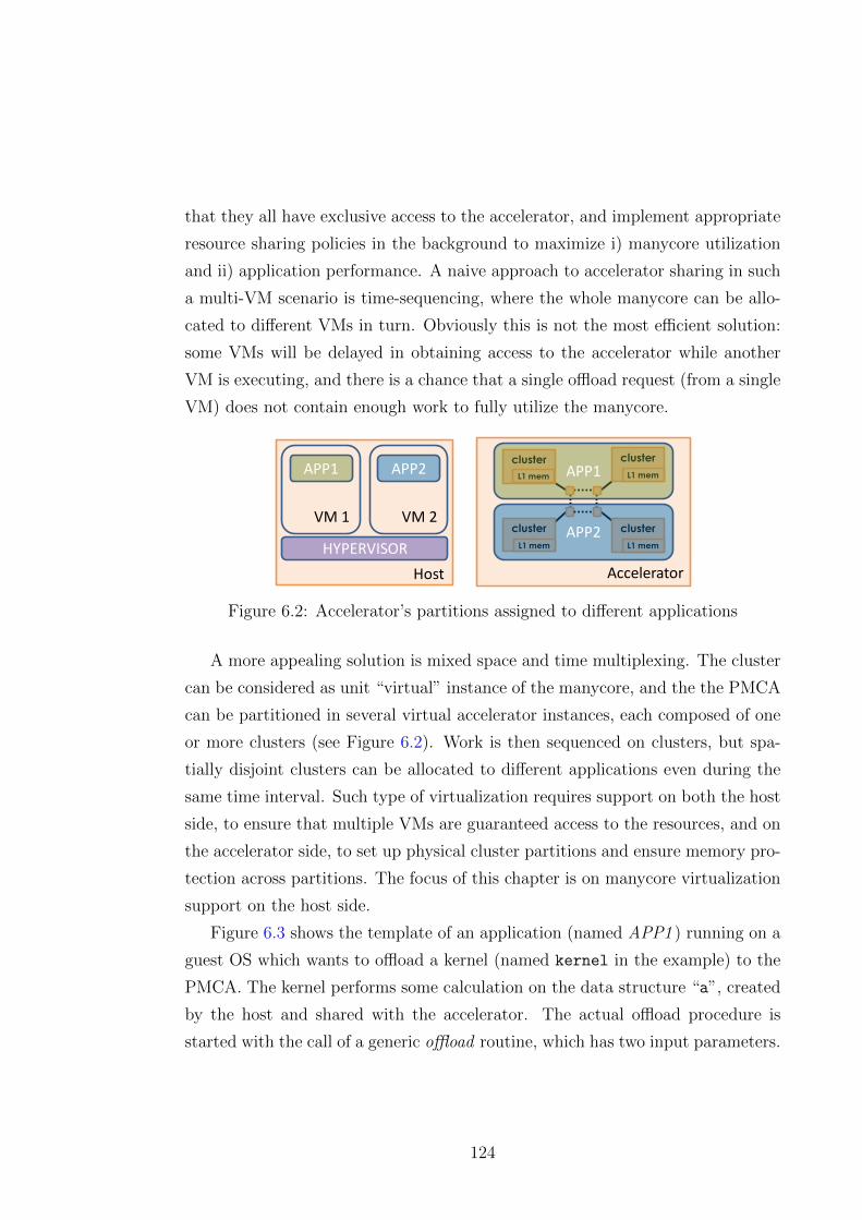
that they all have exclusive access to the accelerator, and implement appropriate
resource sharing policies in the background to maximize i) manycore utilization
and ii) application performance. A naive approach to accelerator sharing in such
a multi-VM scenario is time-sequencing, where the whole manycore can be allo-
cated to different VMs in turn. Obviously this is not the most efficient solution:
some VMs will be delayed in obtaining access to the accelerator while another
VM is executing, and there is a chance that a single offload request (from a single
VM) does not contain enough work to fully utilize the manycore.
cluster
L1 mem
cluster
L1 mem
cluster
L1 mem
cluster
L1 mem
VM 1 VM 2
HYPERVISOR
APP1 APP2 APP1
APP2
Host Accelerator
Figure 6.2: Accelerator’s partitions assigned to different applications
A more appealing solution is mixed space and time multiplexing. The cluster
can be considered as unit “virtual” instance of the manycore, and the the PMCA
can be partitioned in several virtual accelerator instances, each composed of one
or more clusters (see Figure 6.2). Work is then sequenced on clusters, but spa-
tially disjoint clusters can be allocated to different applications even during the
same time interval. Such type of virtualization requires support on both the host
side, to ensure that multiple VMs are guaranteed access to the resources, and on
the accelerator side, to set up physical cluster partitions and ensure memory pro-
tection across partitions. The focus of this chapter is on manycore virtualization
support on the host side.
Figure 6.3 shows the template of an application (named APP1 ) running on a
guest OS which wants to offload a kernel (named kernel in the example) to the
PMCA. The kernel performs some calculation on the data structure “a”, created
by the host and shared with the accelerator. The actual offload procedure is
started with the call of a generic offload routine, which has two input parameters.
124
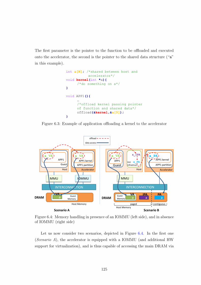
The first parameter is the pointer to the function to be offloaded and executed
onto the accelerator, the second is the pointer to the shared data structure (“a”
in this example).
int a[N]; /*shared between host and
accelerator*/
void kernel(int *a){
/*do something on a*/
}
void APP1(){
…
/*offload kernel passing pointer
of function and shared data*/
offload(&kernel,&a[0]);
}
Figure 6.3: Example of application offloading a kernel to the accelerator
APP1
Host
Guest
a_VA
Accelerator
APP1 partition
a_VA
IOMMUMMU
INTERCONNECTION
offload
APP1
Host
Guest
a_VA
APP1 kernel
Accelerator
APP1 partition
a_PA
MMU
INTERCONNECTION
data access
GuestMemory
a_IPA
a_PA
aGuestMemory a
Host Memory
a a
APP1 kernelVirtInfrastruct.
Scenario A Scenario B
DRAM DRAM
Host Memory paged contiguous
VA IPA PAVA
Figure 6.4: Memory handling in presence of an IOMMU (left side), and in absenceof IOMMU (right side)
Let us now consider two scenarios, depicted in Figure 6.4. In the first one
(Scenario A), the accelerator is equipped with a IOMMU (and additional HW
support for virtualization), and is thus capable of accessing the main DRAM via
125
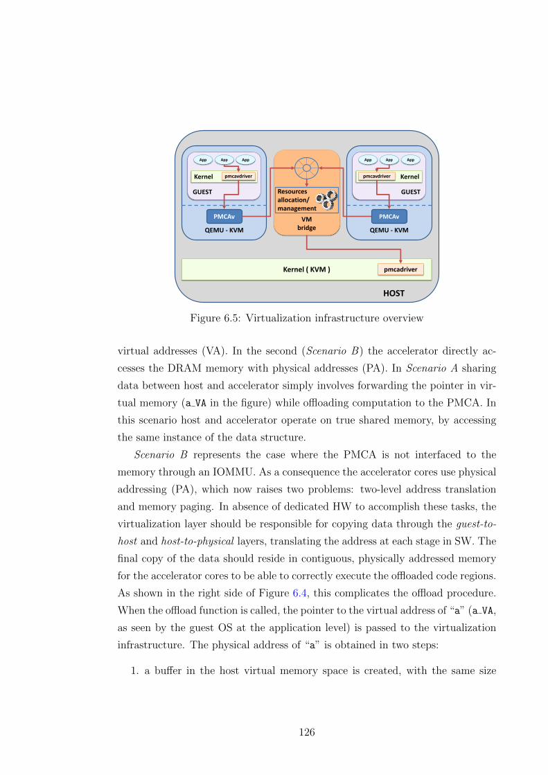
QEMU - KVM
VMbridge
GUEST
Kernel
App App App
pmcavdriver
PMCAv
QEMU - KVM
GUEST
Kernel
App App App
pmcavdriver
PMCAv
Resourcesallocation/management
Kernel ( KVM ) pmcadriver
HOST
Figure 6.5: Virtualization infrastructure overview
virtual addresses (VA). In the second (Scenario B) the accelerator directly ac-
cesses the DRAM memory with physical addresses (PA). In Scenario A sharing
data between host and accelerator simply involves forwarding the pointer in vir-
tual memory (a VA in the figure) while offloading computation to the PMCA. In
this scenario host and accelerator operate on true shared memory, by accessing
the same instance of the data structure.
Scenario B represents the case where the PMCA is not interfaced to the
memory through an IOMMU. As a consequence the accelerator cores use physical
addressing (PA), which now raises two problems: two-level address translation
and memory paging. In absence of dedicated HW to accomplish these tasks, the
virtualization layer should be responsible for copying data through the guest-to-
host and host-to-physical layers, translating the address at each stage in SW. The
final copy of the data should reside in contiguous, physically addressed memory
for the accelerator cores to be able to correctly execute the offloaded code regions.
As shown in the right side of Figure 6.4, this complicates the offload procedure.
When the offload function is called, the pointer to the virtual address of “a” (a VA,
as seen by the guest OS at the application level) is passed to the virtualization
infrastructure. The physical address of “a” is obtained in two steps:
1. a buffer in the host virtual memory space is created, with the same size
126
of “a”, and the original data structure is copied therein. The intermediate
physical address a IPA of this buffer is propagated to the second stage;
2. a buffer is allocated into the contiguous address range of the main memory,
and the target data structure is copied therein.
Once a copy of “a” is available in contiguous memory, a pointer to its physical
address a PA can be forwarded to the PMCA. Note that this solution does not
enable true memory sharing “a” with the host, but rather relies on copies to
replicate the data in linear memory, accessible by the IOMMU-less accelerator.
An identical procedure is applied to every shared data item, and to the pro-
gram binary for the offloaded kernel.
6.5 Implementation
Figure 6.5 depicts the SW infrastructure that we have developed to demonstrate
many-core accelerator virtualization in absence of dedicated HW. We target Linux
ARM hypervisor virtualization, KVM/ARM [44], capable of running unmodified
guest operating systems on ARM (multicore) hardware. Any guest OS, or VM,
at some point during its execution can offload computation to the accelerator.
This intention is expressed in the code using a generic offload API, assuming a
programming model such as OpenMP v4.0 [98] or OpenCL [121].
Whenever an offload is programmed, the compiler and associated runtime
system initialize an offload task descriptor (see Figure 6.6). Such descriptor is
filled with all information needed to handle the offload procedure, including: the
number of clusters needed by the application (num clusters), the pointer to the
code of the kernel and its size (bin ptr, bin size), and a pointer to all shared
data structures (shared data). Shared data structures are annotated at the
application level, using appropriate programming model features (data qualifiers,
clauses, etc.). The compiler creates a marshaling routine, which whenever an
offload occurs fills the shared data field of the descriptor. shared data contains
as many entries as shared data in the program, whose number is annotated in the
127
field num sh data. Each entry is of type mdata, holding the pointer (ptr) and
the size of the shared data structure (size).
struct mdata{
unsigned int size;
void * ptr;
}
struct offload_desc{
unsigned char num_clusters;
unsigned int bin_size;
unsigned char num_sh_data;
void * bin_ptr;
struct mdata * shared_data;
}
Figure 6.6: Task offload descriptor
During the marshaling routine the compiler initializes the shared data ar-
ray with pointers to program variables, which contain the virtual address (a VA
in Figure 6.4). Offload requests are propagated to the physical PMCA device
through four software layers:
1. PMCA virtual driver
2. PMCA virtual device
3. VM BRIDGE
4. PMCA host driver
Each of these SW components is described in the following sections. Through
these layers, binary code of the kernel and data are copied to a region of memory
which is not managed under virtual memory, in order to be accessible by the
PMCA. By default the Linux kernel manages the whole memory available in
the system under virtual memory. At boot time we assign to the Linux Kernel
only a subset of the total system memory, reserving the rest for special use. As
depicted in Figure 6.7 the copies performed are two. The first is used to move
the data from the guest OS virtual memory to the host OS virtual memory, and
128
is performed by the PMCA virtual device. The second copy resolves the last
memory virtualization level, by moving the data in the reserved area of the main
memory, which is not subject to virtual memory paging.
At each step the offload descriptor is updated accordingly to point to these
data copies.
Guest Memory
Host Memory
ContiguousPhysical Memory
Binary Data buf Data buf
Binary Data buf Data buf
Binary Data buf Data buf
1. Copy to host virtual memory space, done by virtual accelerator device
2 . Copy to Contiguous Physical Memory, done by Virtual Machines bridge
Figure 6.7: Data copies performed
PMCA virtual device
GuestVM
PMCAbridge
PMCA Host driver
#pragma omp offload
PMCAvdriver
PMCAdevice
(1) ioctl(offload,task_desc *)
(2) iowrite(tsk_desc *)
Task desc
(3)send_msg(offload,tsk_desc *)
(4)ioctl(offload,tsk_desc *)
Binary and datacopied from Guestvirtual memory toHost virtualmemory
Binary and datacopied from Hostvirtual memory tophysicalcontiguousmemory
num_clusters
bin_size
num_sh_data
bin_ptr
shared_data
Task desc
num_clusters
bin_size
num_sh_data
bin_ptr
shared_data
Task desc
num_clusters
bin_size
num_sh_data
bin_ptr
shared_data
Task desc
num_clusters
bin_size
num_sh_data
bin_ptr
shared_data
Task desc
num_clusters
bin_size
num_sh_data
bin_ptr
shared_data
Figure 6.8: Flow of the offload descriptor through the virtualization infrastructure
129
6.5.1 PMCA virtual driver
The PMCA virtual driver is a standard Linux device driver used to control code
offload to the PMCA. Applications communicate with the driver using the Linux
ioctl system call. Since we adopt a full-virtualization approach, the PMCA vir-
tual and physical driver are identical. However, the virtual driver communicates
to a virtual device, whereas the physical driver communicates to the physical
PMCA. Figure 6.8 depicts the logical flow of a task offload request. The virtual
driver receives via ioctl a pointer to the offload descriptor, which is then copied
into the guest OS kernel space via copy from user and forwarded to the PMCA
virtual device via iowrite (arrows 1 and 2 in Figure 6.8).
6.5.2 PMCA virtual device
Virtual devices are the way KVM emulates I/O devices, and are necessary in a
fully virtualized environment. Virtual machines in KVM are based on QEMU
[25]. The PMCA virtual device is a software module which is developed as an
extension of QEMU. QEMU offers a simple way to enhance its virtual machine
model with custom devices. Once designed each virtual device is attached to the
bus of the platform modeled by QEMU and mapped at a user-defined address
range. Since each guest is executed by an instance of QEMU-KVM, each guest
has a dedicated accelerator’s virtual device. The virtual device is the component
which actually forwards any offload request coming from a VM to the VM bridge.
Any ioread/iowrite issued by applications running on a VM which falls within
the address ranges where the custom devices are mapped, is caught by QEMU and
redirected towards the PMCA virtual device. This virtual device is the crossing
point between the guest OS and the host OS.
Whenever an offload request from a VM arrives to the PMCA virtual device,
it is immediately forwarded to the VM Bridge (arrow 3 in Figure 6.8). At this
stage the first virtualization layer is resolved. A copy of program binary and
shared data is triggered, from the guest OS virtual memory to the host OS virtual
memory space (Figure 6.7). The PMCA virtual device creates a Linux shared
130

memory segment for each data structure to be copied (i.e. one for the binary and
one for each data element). Shared memory is the simplest and most efficient
communication means among different Linux processes (here, QEMU and the
VM bridge). Note that the PMCA virtual device is a process running on the host
OS (it is part of QEMU-KVM), thus the copy process requires to traverse the page
table of the guest OS to access the data. In our framework this is implemented
using a helper function provided by QEMU called cpu memory rw debug. Once
the copy is done, the identifiers of the shared memory segments are annotated
in the offload descriptor and passed to the VM bridge (highlighted in orange in
Figure 6.8).
6.5.3 VM bridge
The VM bridge is a collector of all the offload requests coming from different
VMs in the system. Here it is possible to implement policies to allocate subsets
of PMCA clusters to different VMs (to allow multiple applications or VM to use
the PMCA at the same time). This module is a server process, in charge of
forwarding requests to the PMCA device and providing responses to the various
VM requests. In this component, the second level of memory virtualization is
resolved (Figure 6.7), before the offload descriptor can be forwarded to the next
SW layer.
At startup, this component uses the mmap system call to request the PMCA
host driver to map the reserved contiguous main memory space into the address
map of the VM bridge process. This allows the VM bridge to directly write
into the contiguous memory area. At this point binary and shared data buffers
are copied from the shared memory segments into the contiguous memory via
memcpy.
Once copies are performed, the pointer fields in the offload descriptor are
finally updated with the addresses in physical contiguous memory (highlighted in
light blue in Figure 6.8). The offload descriptor is then forwarded to the PMCA
host driver (arrow 4 in Figure 6.8), using the ioctl system call.
131
6.5.4 PMCA host driver
The same process described for the PMCA virtual driver is used to copy the
offload descriptor into host OS kernel space. The offload descriptor is finally
forwarded to the PMCA device using a sequence of iowrite system calls (arrow
5 in Figure 6.8).
Besides the pure offload of the task, the host driver performs another impor-
tant task. At installation time, the physical memory not used by the linux kernel
during the boot is mapped into the host kernel memory space, using a call to
ioremap nocache. This will allow the bridge process to mmap it. We use the
non-cached version of ioremap to be sure that the data is flushed into memory
immediately when written, avoiding the accelerator to read incorrect data when
the computation is started.
132
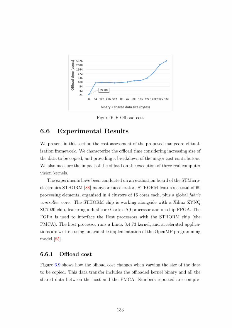
22.80
21
42
84
168
336
672
1344
2688
5376
0 64 128 256 512 1k 4k 8k 16k 32k 128k512k 1M
Off
load
tim
e (u
secs
)
binary + shared data size (bytes)
Figure 6.9: Offload cost
6.6 Experimental Results
We present in this section the cost assessment of the proposed manycore virtual-
ization framework. We characterize the offload time considering increasing size of
the data to be copied, and providing a breakdown of the major cost contributors.
We also measure the impact of the offload on the execution of three real computer
vision kernels.
The experiments have been conducted on an evaluation board of the STMicro-
electronics STHORM [88] manycore accelerator. STHORM features a total of 69
processing elements, organized in 4 clusters of 16 cores each, plus a global fabric
controller core. The STHORM chip is working alongside with a Xilinx ZYNQ
ZC7020 chip, featuring a dual core Cortex-A9 processor and on-chip FPGA. The
FGPA is used to interface the Host processors with the STHORM chip (the
PMCA). The host processor runs a Linux 3.4.73 kernel, and accelerated applica-
tions are written using an available implementation of the OpenMP programming
model [85].
6.6.1 Offload cost
Figure 6.9 shows how the offload cost changes when varying the size of the data
to be copied. This data transfer includes the offloaded kernel binary and all the
shared data between the host and the PMCA. Numbers reported are compre-
133
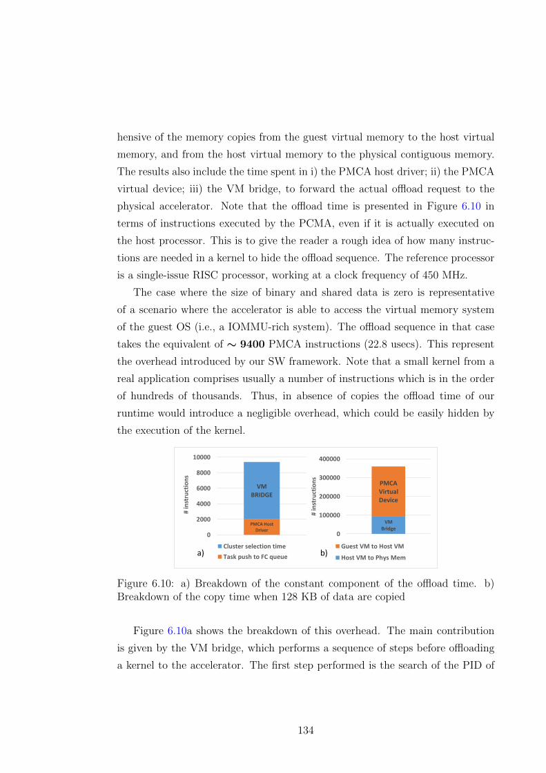
hensive of the memory copies from the guest virtual memory to the host virtual
memory, and from the host virtual memory to the physical contiguous memory.
The results also include the time spent in i) the PMCA host driver; ii) the PMCA
virtual device; iii) the VM bridge, to forward the actual offload request to the
physical accelerator. Note that the offload time is presented in Figure 6.10 in
terms of instructions executed by the PCMA, even if it is actually executed on
the host processor. This is to give the reader a rough idea of how many instruc-
tions are needed in a kernel to hide the offload sequence. The reference processor
is a single-issue RISC processor, working at a clock frequency of 450 MHz.
The case where the size of binary and shared data is zero is representative
of a scenario where the accelerator is able to access the virtual memory system
of the guest OS (i.e., a IOMMU-rich system). The offload sequence in that case
takes the equivalent of ∼ 9400 PMCA instructions (22.8 usecs). This represent
the overhead introduced by our SW framework. Note that a small kernel from a
real application comprises usually a number of instructions which is in the order
of hundreds of thousands. Thus, in absence of copies the offload time of our
runtime would introduce a negligible overhead, which could be easily hidden by
the execution of the kernel.
VM Bridge
PMCA Virtual Device
0
100000
200000
300000
400000
# in
stru
ctio
ns
Guest VM to Host VM
Host VM to Phys Mem
PMCA Host Driver
VM BRIDGE
0
2000
4000
6000
8000
10000
# in
stru
ctio
ns
Cluster selection time
Task push to FC queue b)a)
Figure 6.10: a) Breakdown of the constant component of the offload time. b)Breakdown of the copy time when 128 KB of data are copied
Figure 6.10a shows the breakdown of this overhead. The main contribution
is given by the VM bridge, which performs a sequence of steps before offloading
a kernel to the accelerator. The first step performed is the search of the PID of
134
the Virtual Machine process in the VMs list, to check whether it is authorized
to offload a task. The second step is the creation of a clusters bitmask, which
encodes information about the number and ID of the clusters assigned to the
requesting VM, later forwarded to the fabric controller.
The second component shown in Figure 6.10a is the PMCA host driver, per-
forming ioread/iowrite operations to push the offload data structure into the
fabric controller offload manager. It is possible to notice that no components
related to the PMCA virtual driver and to the PMCA virtual device have been
taken into account. The former is negligible with respect to the other components.
The latter is absent when the size of the copied data is null.
6.6.2 Memory copies breakdown
In the previous sections, only the cost for the offload procedure is considered. In
this paragraph we discuss how memory copies are distributed along the virtual-
ization chain.
Figure 6.10b shows the breakdown of the memory copy time (128 KBytes),
which highlights the two main contributors. The first is introduced by the virtual
machine bridge, where binary and shared buffers are copied from the guest virtual
memory to the host virtual memory. Here binary and shared buffers are copied
into a shared memory segment of the Linux OS, to be shared with other processes
(the VM bridge). The second component is the VM bridge. Here both binary
and buffers are copied into the contiguous area of the main memory, which has
already been mmap-ped to the VM bridge virtual memory map.
It is immediate to see that the first component represents most of the copy
overhead. This happens because the copy from guest OS to host OS virtual
memory is implemented using an helper function in QEMU, which is traversing
the guest OS page table to access the data to be copied, plus memcpy.
135
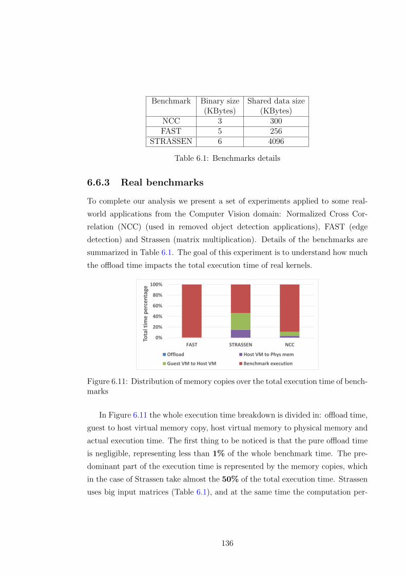
Benchmark Binary size Shared data size(KBytes) (KBytes)
NCC 3 300FAST 5 256
STRASSEN 6 4096
Table 6.1: Benchmarks details
6.6.3 Real benchmarks
To complete our analysis we present a set of experiments applied to some real-
world applications from the Computer Vision domain: Normalized Cross Cor-
relation (NCC) (used in removed object detection applications), FAST (edge
detection) and Strassen (matrix multiplication). Details of the benchmarks are
summarized in Table 6.1. The goal of this experiment is to understand how much
the offload time impacts the total execution time of real kernels.
0%
20%
40%
60%
80%
100%
FAST STRASSEN NCC
Tota
l tim
e p
erc
en
tage
Offload Host VM to Phys mem
Guest VM to Host VM Benchmark execution
Figure 6.11: Distribution of memory copies over the total execution time of bench-marks
In Figure 6.11 the whole execution time breakdown is divided in: offload time,
guest to host virtual memory copy, host virtual memory to physical memory and
actual execution time. The first thing to be noticed is that the pure offload time
is negligible, representing less than 1% of the whole benchmark time. The pre-
dominant part of the execution time is represented by the memory copies, which
in the case of Strassen take almost the 50% of the total execution time. Strassen
uses big input matrices (Table 6.1), and at the same time the computation per-
136
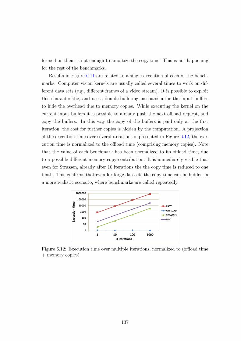
formed on them is not enough to amortize the copy time. This is not happening
for the rest of the benchmarks.
Results in Figure 6.11 are related to a single execution of each of the bench-
marks. Computer vision kernels are usually called several times to work on dif-
ferent data sets (e.g., different frames of a video stream). It is possible to exploit
this characteristic, and use a double-buffering mechanism for the input buffers
to hide the overhead due to memory copies. While executing the kernel on the
current input buffers it is possible to already push the next offload request, and
copy the buffers. In this way the copy of the buffers is paid only at the first
iteration, the cost for further copies is hidden by the computation. A projection
of the execution time over several iterations is presented in Figure 6.12, the exe-
cution time is normalized to the offload time (comprising memory copies). Note
that the value of each benchmark has been normalized to its offload time, due
to a possible different memory copy contribution. It is immediately visible that
even for Strassen, already after 10 iterations the the copy time is reduced to one
tenth. This confirms that even for large datasets the copy time can be hidden in
a more realistic scenario, where benchmarks are called repeatedly.
1
10
100
1000
10000
100000
1000000
1 10 100 1000
Exec
uti
on
tim
e
# iterations
FAST
OFFLOAD
STRASSEN
NCC
Figure 6.12: Execution time over multiple iterations, normalized to (offload time+ memory copies)
137
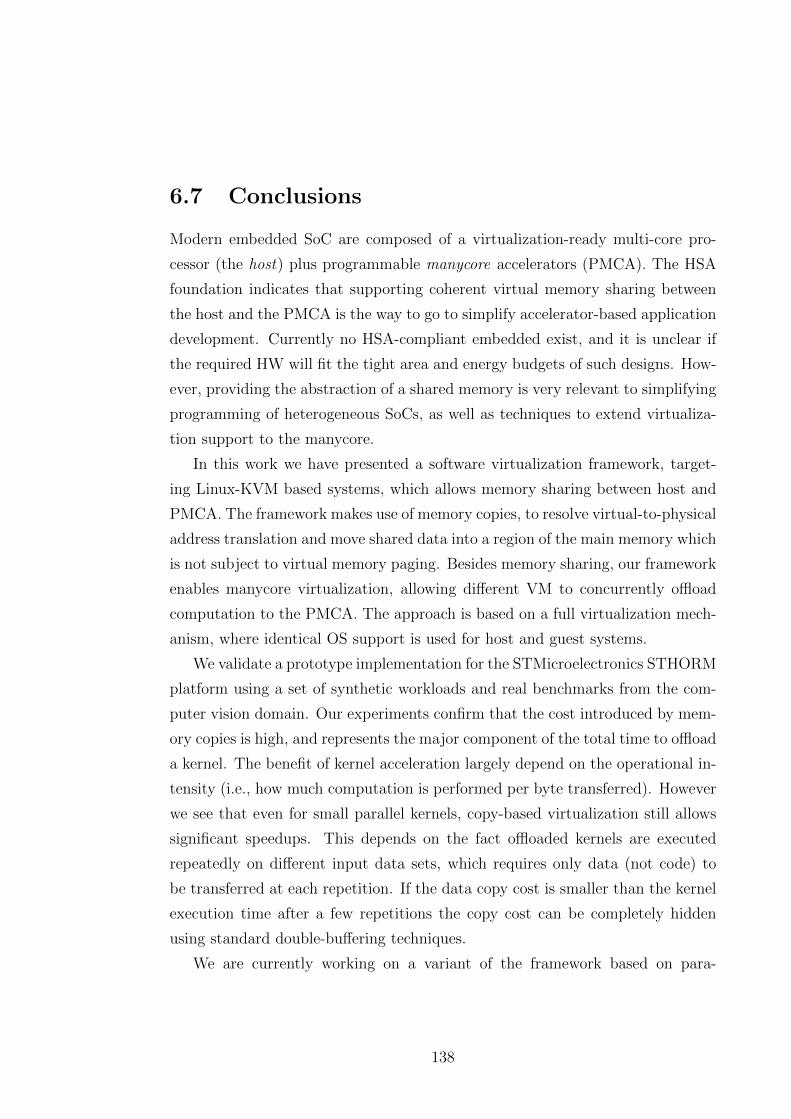
6.7 Conclusions
Modern embedded SoC are composed of a virtualization-ready multi-core pro-
cessor (the host) plus programmable manycore accelerators (PMCA). The HSA
foundation indicates that supporting coherent virtual memory sharing between
the host and the PMCA is the way to go to simplify accelerator-based application
development. Currently no HSA-compliant embedded exist, and it is unclear if
the required HW will fit the tight area and energy budgets of such designs. How-
ever, providing the abstraction of a shared memory is very relevant to simplifying
programming of heterogeneous SoCs, as well as techniques to extend virtualiza-
tion support to the manycore.
In this work we have presented a software virtualization framework, target-
ing Linux-KVM based systems, which allows memory sharing between host and
PMCA. The framework makes use of memory copies, to resolve virtual-to-physical
address translation and move shared data into a region of the main memory which
is not subject to virtual memory paging. Besides memory sharing, our framework
enables manycore virtualization, allowing different VM to concurrently offload
computation to the PMCA. The approach is based on a full virtualization mech-
anism, where identical OS support is used for host and guest systems.
We validate a prototype implementation for the STMicroelectronics STHORM
platform using a set of synthetic workloads and real benchmarks from the com-
puter vision domain. Our experiments confirm that the cost introduced by mem-
ory copies is high, and represents the major component of the total time to offload
a kernel. The benefit of kernel acceleration largely depend on the operational in-
tensity (i.e., how much computation is performed per byte transferred). However
we see that even for small parallel kernels, copy-based virtualization still allows
significant speedups. This depends on the fact offloaded kernels are executed
repeatedly on different input data sets, which requires only data (not code) to
be transferred at each repetition. If the data copy cost is smaller than the kernel
execution time after a few repetitions the copy cost can be completely hidden
using standard double-buffering techniques.
We are currently working on a variant of the framework based on para-
138
virtualization. While this requires modifications to the guest OS, it allows to
reduce the number of copies required to enable shared memory host-to-PMCA
communication.
139

140
Chapter 7
Conclusions
The astonishing computing power of many-core architectures does not come for
free. Designers and programmers of such platforms have today to tackle several
challenge obtain the maximum possible performance. The memory wall, and the
complexity of the chip design itself are the two most known challenges, but other
still need to be tackled. In this thesis various virtualization techniques are pre-
sented with the aim of overcoming, or mitigating, some of the aforementioned
challenges. First of all the design exploration complexity problem is tackled with
a SystemC based virtual platform VirtualSoC, enabling the designer to easily
have a forecast of power/performance implication of his design choices. Virtu-
alSoC can be also used by programmers and programming models designers to
develop software runtimes before the hardware is actually available. Virtual Plat-
forms allow also to study future hardware platforms, targeting systems composed
by thousands of computational units. However increasing the size of the system
being modeled increases also the the run time and the complexity of a simula-
tion, forcing users to often trade accuracy for speed. In this thesis a technique
is presented, which allows to speed-up the simulation at the instruction level ac-
curacy of a thousand-core chip by exploiting the massively parallel hardware of
off-the-shelf GP-GPU cards. Results showed that the proposed technique can
outperform classic sequential simulation tools, when the size of the target system
increases.
141
However, the hardware design is not the only side of the coin being challenged
by modern systems. Many-core chips provide high computational power which is
not straightforward for programmers to be achieved. One example is the memory
bandwidth wall, caused by the always increasing clock frequency of processing
units not followed by actual DRAM technology. Programmers are thus forced
to minimize the number of external memory accesses, using as much as possible
the faster on-chip memory modules. Nonetheless the data set for a real-world
application is not likely to fit inside on-chip memories, and programmers usually
have to implement swap-in swap-out mechanisms to overlap the computation
with the memory access. In this dissertation a memory virtualization framework
is presented to the the programmer in automatically transfer the data needed
from to the external memory. The results showed that the performance obtained
is comparable with that of a hand tuned DMA bouble-buffering pattern, but with
∼ 20% reduction in the size of the code.
Finally virtualization has been applied at its higher level of abstraction, tar-
geting the virtualization of a many-core accelerator in a Linux-KVM environment.
The goal is to exploit the parallel (clustered) nature of a typical many-core chip
the be shared by several virtual machines, running on the same host system. The
work presented is composed by a modified release of the OpenMP programming
paradigm adapted to offload code to a general purpose accelerator, and by a
virtualization framework in charge of collecting requests from the various virtual
machines and actually offload each of them to the accelerator. This work had also
the goal of solving a very important issue of Host-Accelerator systems: memory
sharing between host and accelerator. experimental results show that the offload
procedure passing through the virtualization framework introduces a negligible
overhead with respect to the whole execution of a parallel kernel, and that the
inability to efficiently share memory is a serious performance limiting factor.
142
7.1 Future research directions
The present dissertation could be considered as a starting point for various re-
search directions, the most important are summarize din the following list.
� Virtual Platforms : Thanks to design of VirtualSoC, HW/SW developers
are provided with a tool which enables the full-system simulation of mod-
ern many-core embedded systems capturing host-accelerator interaction.
And as far as our knowledge, it is the first platform capturing such inter-
actions. VirtualSoC can be used both from the HW designer, to perform
a fast design space exploration to drive his design process towards the best
hardware implementation. On the Other side VirtualSoC can be used by
software programmers to test their software, and to develop parallel pro-
gramming models. Thanks to the high detailed simulation of the accel-
erator, the programming model researcher can experiment the benefits of
specific hardware support to software execution. As an example it is pos-
sible to model various inter-processor communication facilities, and study
their effects on the on applications performance.
� Memory Virtualization - Software cache: The work presented in this
thesis focuses on memory virtualization for a single cluster of a many-core
multi-cluster embedded accelerator. Experimental results showed that the
proposed design is highly optimized, and permits to almost fully exploit the
on-chip memory on each cluster. Next research direction can be focused
on the extension of the software cache to a multi-cluster cooperative
framework, in which the software caches on each cluster communicate with
the aim of further reducing the need to access the off-chip memory. This in
turn makes room for research of cache coherency protocols in a multi-cluster
many-core embedded system. In addition most multi-cluster accelerators
embed also a second level data scratchpad which is shared among all
the clusters. Such memory layer can be exploited to function as a sec-
ond level software cache, with the goal of reducing the average miss latency.
143
� Virtualization of many-core accelerators : The virtualization of a many-core
accelerators is today a hot research topic since the use of virtual machines
has become a requirement for server/cloud computing platforms, and ap-
plications rely more and more on accelerators to achieve an always higher
computing performance. The research presented in this dissertation is to be
considered as the initial brick in the definition of a well established virtu-
alization technique, by highlighting the weaknesses (e.g. lack of IOMMU)
of current hardware platforms and defining a first proposal virtualization
infrastructure based on Linux/KVM.
144
Publications
2010
� Shivani Raghav, Martino Ruggiero, David Atienza, Christian Pinto, An-
drea Marongiu and Luca Benini. Scalable instruction set simulator for
thousand-core architectures running on GPGPUs. In: High Performance
Computing and Simulation (HPCS), 2010 International Conference on,
pages 459 -466, 2010.
2011
� Christian Pinto, Shivani Raghav, Andrea Marongiu, Martino Ruggiero,
David Atienza and Luca Benini. GPGPU-Accelerated Parallel and Fast
Simulation of Thousand-core Platforms. In: International Symposium on
Cluster, Cloud and Grid Computing (CCGRID), pages 53-62, 2011.
� Daniele Bortolotti, Francesco Paterna, Christian Pinto, Andrea
Marongiu, Martino Ruggiero, and Luca Benini. Exploring instruction
caching strategies for tightly-coupled shared-memory clusters. In: System
on Chip (SoC), 2011 International Symposium on, pages 34–41. IEEE,
2011.
2012
� Shivani Raghav, Andrea Marongiu, Christian Pinto, David Atienza, Mar-
tino Ruggiero and Luca Benini. Full System Simulation of Many-Core Het-
erogeneous SoCs using GPU and QEMU Semihosting. In: GPGPU-5, pages
101-109, ACM, 2012
145
� Shivani Raghav, Andrea Marongiu, Christian Pinto, Martino Ruggiero,
David Atienza and Luca Benini. SIMinG-1k: A Thousand-Core Simulator
running on GPGPUs. In: Concurrency and Computation: Practice and
Experience, pages 1–18, 2012.
2013
� Christian Pinto and Luca Benini. A Highly Efficient, Thread-Safe Soft-
ware Cache Implementation for Tightly-Coupled Multicore Clusters. In:
The 24th IEEE International Conference on Application-specific Systems,
Architectures and Processors (ASAP13), pages 281-288, IEEE, 2013
� Daniele Bortolotti, Christian Pinto, Andrea Marongiu, Martino Ruggiero,
and Luca Benini. Virtualsoc: A full-system simulation environment for
massively parallel heterogeneous system-on-chip. In: Proceedings of the
2013 IEEE 27th International Symposium on Parallel and Distributed Pro-
cessing Workshops and PhD Forum, pages 2182–2187. IEEE Computer
Society, 2013.
2014
� Christian Pinto and Luca Benini. A Novel Object-Oriented Software
Cache for Scratchpad-Based Multi-Core Clusters. In: Journal of Signal
Processing Systems, Volume 77, Issue 1-2 , pages 77–93 , Springer, 2014.
� Christian Pinto, Andrea Marongiu and Luca Benini. A Virtualization
Framework for IOMMU-less Many-Core Accelerators. In: MES 2014 (colo-
cated with ISCA 2014), ACM, 2014.
� Christian Pinto and Luca Benini. Exploring DMA-assisted Prefetch-
ing Strategies for Software Caches on Multicore Clusters. In: The 24th
IEEE International Conference on Application-specific Systems, Architec-
tures and Processors (ASAP14), pages 224–231, IEEE, 2014.
146
� Shivani Raghav, Martino Ruggiero, Andrea Marongiu, Christian Pinto,
David Atienza and Luca Benini. GPU Acceleration for simulating mas-
sively parallel many-core platforms. In: IEEE Transactions on Parallel and
Distributed Systems, IEEE, 2014.
147

148
Bibliography
[1] Introduction to AMBA®4 ACE�and big.LITTLE�Processing Technology.
121, 122
[2] Eurocloud european project website. URL http://www.eurocloudserver.
com/. 35
[3] Montblanc project. URL http://www.montblanc-project.eu/. 1
[4] NVIDIA CUDA Programming Guide, 2007. URL http://developer.
download.nvidia.com/compute/cuda/1_0/NVIDIA_CUDA_Programming_
Guide_1.0.pdf. 34
[5] CUDA: Scalable parallel programming for high-performance scientific com-
puting, June 2008. doi: 10.1109/ISBI.2008.4541126. URL http://dx.doi.
org/10.1109/ISBI.2008.4541126. 35
[6] Plurality ltd. - the hypercore processor, 2012. URL http://www.
plurality.com/hypercore.html. 11, 123
[7] SystemC 2.3.0 Users Guide. 2012. 6, 22
[8] Adapteva Inc. Parallela Reference Manual. URL www.parallella.org/
wp-content/uploads/2013/01/parallella_gen1_reference.pdf. 117,
119, 122
[9] Advanced Micro Devices, Inc. AMD I/O Virtualization Tech-
nology (IOMMU) Specification. URL support.amd.com/TechDocs/
34434-IOMMU-Rev_1.26_2-11-09.pdf. 119, 122
149
[10] Advanced Micro Devices, Inc. AMD A-Series APU Proces-
sors. URL www.amd.com/us/products/desktop/processors/a-series/
Pages/a-series-apu.aspx. 119, 121
[11] Vikas Agarwal, MS Hrishikesh, Stephen W Keckler, and Doug Burger.
Clock rate versus ipc: The end of the road for conventional microarchi-
tectures. volume 28, pages 248–259. ACM, 2000. 7, 8
[12] Aneesh Aggarwal. Software caching vs. prefetching. SIGPLAN Not., 38(2
supplement):157–162, June 2002. ISSN 0362-1340. doi: 10.1145/773039.
512450. URL http://doi.acm.org/10.1145/773039.512450. 65
[13] Eduardo Argollo, Ayose Falcon, Paolo Faraboschi, Matteo Monchiero, and
Daniel Ortega. Cotson: infrastructure for full system simulation. Operating
Systems Review, 43(1):52–61, 2009. 36
[14] ARM Ltd. ARM Architecture Reference Manual ARMv7-A and ARMv7-R
Edition. URL infocenter.arm.com/help/index.jsp?topic=/com.arm.
doc.ddi0406b/index.html. 120
[15] ARM Ltd. Virtualization is Coming to a Platform Near You, 2012.
URL http://mobile.arm.com/files/pdf/System-MMU-Whitepaper-v8.
0.pdf. iv, 5, 121, 123
[16] Krste Asanovic, Rastislav Bodik, James Demmel, Tony Keaveny, Kurt
Keutzer, John Kubiatowicz, Nelson Morgan, David Patterson, Koushik
Sen, John Wawrzynek, David Wessel, and Katherine Yelick. A view of the
parallel computing landscape. Commun. ACM, 52(10):56–67, 2009. ISSN
0001-0782. doi: http://doi.acm.org/10.1145/1562764.1562783. 34, 38
[17] Arnaldo Azevedo and Ben Juurlink. An instruction to accelerate soft-
ware caches. In Mladen Berekovic, William Fornaciari, Uwe Brinkschulte,
and Cristina Silvano, editors, Architecture of Computing Systems - ARCS
2011, volume 6566 of Lecture Notes in Computer Science, pages 158–
150
170. Springer Berlin Heidelberg, 2011. ISBN 978-3-642-19136-7. doi:
10.1007/978-3-642-19137-4\ 14. 66
[18] Arnaldo Azevedo and Ben H. H. Juurlink. A multidimensional software
cache for scratchpad-based systems. IJERTCS, 1(4):1–20, 2010. doi: http:
//dx.doi.org/10.4018/jertcs.2010100101. 66
[19] Jairo Balart, Marc Gonzalez, Xavier Martorell, Eduard Ayguade, Zehra
Sura, Tong Chen, Tao Zhang, Kevin OBrien, and Kathryn OBrien. A novel
asynchronous software cache implementation for the cell-be processor. In
Vikram Adve, MaraJess Garzarn, and Paul Petersen, editors, Languages
and Compilers for Parallel Computing, volume 5234 of Lecture Notes in
Computer Science, pages 125–140. Springer Berlin Heidelberg, 2008. ISBN
978-3-540-85260-5. doi: 10.1007/978-3-540-85261-2\ 9. 63, 67
[20] Rajeshwari Banakar, Stefan Steinke, Bo-Sik Lee, M. Balakrishnan, and
Peter Marwedel. Scratchpad memory: design alternative for cache on-chip
memory in embedded systems. In Proceedings of the tenth international
symposium on Hardware/software codesign, CODES ’02, pages 73–78, New
York, NY, USA, 2002. ACM. ISBN 1-58113-542-4. doi: 10.1145/774789.
774805. URL http://doi.acm.org/10.1145/774789.774805. 4, 62, 97
[21] Paul Barham, Boris Dragovic, Keir Fraser, Steven Hand, Tim Harris, Alex
Ho, Rolf Neugebauer, Ian Pratt, and Andrew Warfield. Xen and the art
of virtualization. SIGOPS Oper. Syst. Rev., 37(5):164–177, October 2003.
ISSN 0163-5980. doi: 10.1145/1165389.945462. URL http://doi.acm.
org/10.1145/1165389.945462. iii
[22] Michela Becchi, Kittisak Sajjapongse, Ian Graves, Adam Procter, Vi-
gnesh Ravi, and Srimat Chakradhar. A virtual memory based run-
time to support multi-tenancy in clusters with gpus. In Proceedings of
the 21st International Symposium on High-Performance Parallel and Dis-
tributed Computing, HPDC ’12, pages 97–108, New York, NY, USA, 2012.
151
ACM. ISBN 978-1-4503-0805-2. doi: 10.1145/2287076.2287090. URL
http://doi.acm.org/10.1145/2287076.2287090. 121
[23] Nathan Beckmann, Jonathan Eastep, Charles Gruenwald, George Kurian,
Harshad Kasture, Jason E. Miller, Christopher Celio, and Anant Agarwal.
Graphite: A Distributed Parallel Simulator for Multicores. Technical re-
port, MIT, November 2009. URL http://dspace.mit.edu/handle/1721.
1/49809. 34, 37
[24] Robert Bedichek. Simnow: Fast platform simulation purely in software. In
Hot Chips, volume 16, 2004. 3, 18, 37
[25] Fabrice Bellard. Qemu, a fast and portable dynamic translator. In USENIX
2005 Annual Technical Conference, FREENIX Track, pages 41–46, 2005.
6, 18, 36, 130
[26] Luca Benini and Giovanni De Micheli. Networks on chips: A new soc
paradigm. Computer, 35(1):70–78, 2002. 9
[27] Luca Benini, Eric Flamand, Didier Fuin, and Diego Melpignano. P2012:
Building an ecosystem for a scalable, modular and high-efficiency embed-
ded computing accelerator. In Proceedings of the Conference on Design,
Automation and Test in Europe, pages 983–987. EDA Consortium, 2012. 8,
9, 10, 67
[28] Nathan L. Binkert, Ronald G. Dreslinski, Lisa R. Hsu, Kevin T. Lim, Ali G.
Saidi, and Steven K. Reinhardt. The m5 simulator: Modeling networked
systems. IEEE Micro, 26(4):52–60, 2006. ISSN 0272-1732. doi: http:
//dx.doi.org/10.1109/MM.2006.82. 36
[29] Patrick Bohrer, James Peterson, Mootaz Elnozahy, Ram Rajamony, Ahmed
Gheith, Ron Rockhold, Charles Lefurgy, Hazim Shafi, Tarun Nakra, Rick
Simpson, Evan Speight, Kartik Sudeep, Eric Van Hensbergen, and Lixin
Zhang. Mambo: a full system simulator for the powerpc architecture. SIG-
METRICS Perform. Eval. Rev., 31(4):8–12, 2004. 3, 18
152
[30] Shekhar Borkar. Thousand core chips: a technology perspective. In Pro-
ceedings of the 44th annual Design Automation Conference, DAC ’07, pages
746–749, New York, NY, USA, 2007. ACM. ISBN 978-1-59593-627-1. doi:
10.1145/1278480.1278667. URL http://doi.acm.org/10.1145/1278480.
1278667. 33, 61, 62
[31] Shekhar Borkar and Andrew A Chien. The future of microprocessors. In
Communications of the ACM, volume 54, pages 67–77. ACM, 2011. 7, 8
[32] G. Bradski. The OpenCV Library. Dr. Dobb’s Journal of Software Tools,
2000. 75
[33] Nathan Brookwood. Amd fusion family of apus: enabling a superior, im-
mersive pc experience. Insight, 64(1):1–8, 2010. 8, 16, 61, 97
[34] David Callahan, Ken Kennedy, and Allan Porterfield. Software prefetching.
SIGPLAN Not., 26(4):40–52, April 1991. ISSN 0362-1340. doi: 10.1145/
106973.106979. URL http://doi.acm.org/10.1145/106973.106979. 65,
99
[35] D. Chatterjee, A. DeOrio, and V. Bertacco. Event-driven gate-level sim-
ulation with gp-gpus. In Design Automation Conference, 2009. DAC ’09.
46th ACM/IEEE, pages 557 –562, july 2009. 37
[36] Chen Chen, JosephB Manzano, Ge Gan, GuangR. Gao, and Vivek Sarkar.
A study of a software cache implementation of the openmp memory model
for multicore and manycore architectures. In Pasqua DAmbra, Mario
Guarracino, and Domenico Talia, editors, Euro-Par 2010 - Parallel Pro-
cessing, volume 6272 of Lecture Notes in Computer Science, pages 341–
352. Springer Berlin Heidelberg, 2010. ISBN 978-3-642-15290-0. doi:
10.1007/978-3-642-15291-7\ 31. 67, 100
[37] Tong Chen, Tao Zhang, Zehra Sura, and Mar Gonzales Tallada. Prefetch-
ing irregular references for software cache on cell. In Proceedings of
the 6th annual IEEE/ACM international symposium on Code generation
153
and optimization, CGO ’08, pages 155–164, New York, NY, USA, 2008.
ACM. ISBN 978-1-59593-978-4. doi: 10.1145/1356058.1356079. URL
http://doi.acm.org/10.1145/1356058.1356079. 66, 100, 101
[38] Derek Chiou, Dam Sunwoo, Joonsoo Kim, Nikhil A. Patil, William Rein-
hart, Darrel Eric Johnson, Jebediah Keefe, and Hari Angepat. Fpga-
accelerated simulation technologies (fast): Fast, full-system, cycle-accurate
simulators. In Proceedings of the 40th Annual IEEE/ACM International
Symposium on Microarchitecture, MICRO 40, pages 249–261, Washing-
ton, DC, USA, 2007. IEEE Computer Society. ISBN 0-7695-3047-8. doi:
http://dx.doi.org/10.1109/MICRO.2007.16. URL http://dx.doi.org/
10.1109/MICRO.2007.16. 37
[39] Intel Corp. Single-chip cloud computer.
http://techresearch.intel.com/articles/Tera-Scale/1826.htm. 34, 38
[40] Tilera Corporation. Tilera processors, 2013. URL http://www.tilera.
com/products/processors. 8
[41] Rita Cucchiara, Andrea Prati, and Massimo Piccardi. Improving data
prefetching efficacy in multimedia applications. Multimedia Tools and Ap-
plications, 20(2):159–178, 2003. 99
[42] Leonardo Dagum and Ramesh Menon. Openmp: an industry standard api
for shared-memory programming. Computational Science & Engineering,
IEEE, 5(1):46–55, 1998. 11
[43] F. Dahlgren, Michel Dubois, and P. Stenstrom. Sequential hardware
prefetching in shared-memory multiprocessors. Parallel and Distributed
Systems, IEEE Transactions on, 6(7):733–746, 1995. ISSN 1045-9219. doi:
10.1109/71.395402. 99
[44] Christoffer Dall and Jason Nieh. Kvm/arm: The design and implementa-
tion of the linux arm hypervisor. In Proceedings of the 19th International
154
Conference on Architectural Support for Programming Languages and Op-
erating Systems, ASPLOS ’14, pages 333–348, New York, NY, USA, 2014.
ACM. ISBN 978-1-4503-2305-5. doi: 10.1145/2541940.2541946. URL
http://doi.acm.org/10.1145/2541940.2541946. 127
[45] William J Dally and Brian Towles. Route packets, not wires: On-chip inter-
connection networks. In Design Automation Conference, 2001. Proceedings,
pages 684–689. IEEE, 2001. 9
[46] Samir Das, Richard Fujimoto, Kiran Panesar, Don Allison, and Maria Hy-
binette. Gtw: A time warp system for shared memory multiprocessors. In
in Proceedings of the 1994 Winter Simulation Conference, pages 1332–1339,
1994. 37
[47] M. Dasygenis, E. Brockmeyer, B. Durinck, F. Catthoor, D. Soudris, and
A. Thanailakis. A combined dma and application-specific prefetching ap-
proach for tackling the memory latency bottleneck. Very Large Scale Inte-
gration (VLSI) Systems, IEEE Transactions on, 14(3):279–291, 2006. ISSN
1063-8210. doi: 10.1109/TVLSI.2006.871759. 100
[48] W. Rhett Davis, John Wilson, Stephen Mick, Jian Xu, Hao Hua, Christo-
pher Mineo, Ambarish M. Sule, Michael Steer, and Paul D. Franzon.
Demystifying 3d ics: The pros and cons of going vertical. IEEE De-
sign and Test of Computers, 22:498–510, 2005. ISSN 0740-7475. doi:
http://doi.ieeecomputersociety.org/10.1109/MDT.2005.136. 34
[49] Phillip M. Dickens, Philip Heidelberger, and David M. Nicol. A distributed
memory lapse: Parallel simulation of message-passing programs. In In
Workshop on Parallel and Distributed Simulation, pages 32–38, 1993. 37
[50] A. E. Eichenberger, J. K. O’Brien, K. M. O’Brien, P. Wu, T. Chen, P. H.
Oden, D. A. Prener, J. C. Shepherd, B. So, Z. Sura, A. Wang, T. Zhang,
P. Zhao, M. K. Gschwind, R. Archambault, Y. Gao, and R. Koo. Using
advanced compiler technology to exploit the performance of the Cell Broad-
155
band Engine� architecture. IBM Systems Journal, 45(1):59 –84, 2006. ISSN
0018-8670. doi: 10.1147/sj.451.0059. 67
[51] Yoav Freund and RobertE. Schapire. A desicion-theoretic generalization
of on-line learning and an application to boosting. In Paul Vitnyi, editor,
Computational Learning Theory, volume 904 of Lecture Notes in Computer
Science, pages 23–37. Springer Berlin Heidelberg, 1995. ISBN 978-3-540-
59119-1. doi: 10.1007/3-540-59119-2\ 166. URL http://dx.doi.org/10.
1007/3-540-59119-2_166. 92
[52] David Geer. Chip makers turn to multicore processors. volume 38, pages
11–13. IEEE, 2005. 7, 8
[53] Gideon Glass and Pei Cao. Adaptive page replacement based on mem-
ory reference behavior. In Proceedings of the 1997 ACM SIGMETRICS
international conference on Measurement and modeling of computer sys-
tems, SIGMETRICS ’97, pages 115–126, New York, NY, USA, 1997.
ACM. ISBN 0-89791-909-2. doi: 10.1145/258612.258681. URL http:
//doi.acm.org/10.1145/258612.258681. 65
[54] Marius Gligor and Frederic Petrot. Combined use of dynamic binary trans-
lation and systemc for fast and accurate mpsoc simulation. In 1st Interna-
tional QEMU Users’ Forum, volume 1, pages 19–22, March 2011. 19
[55] Simcha Gochman, Avi Mendelson, Alon Naveh, and Efraim Rotem. Intro-
duction to intel core duo processor architecture. Intel Technology Journal,
10(2), 2006. 8
[56] Marc Gonzalez, Nikola Vujic, Xavier Martorell, Eduard Ayguade, Alexan-
dre E. Eichenberger, Tong Chen, Zehra Sura, Tao Zhang, Kevin O’Brien,
and Kathryn O’Brien. Hybrid access-specific software cache techniques for
the cell be architecture. In Proceedings of the 17th international confer-
ence on Parallel architectures and compilation techniques, PACT ’08, pages
292–302, New York, NY, USA, 2008. ACM. ISBN 978-1-60558-282-5. doi:
156
10.1145/1454115.1454156. URL http://doi.acm.org/10.1145/1454115.
1454156. 67
[57] Thorsten Grotker. System Design with SystemC. Kluwer Academic Pub-
lishers, Norwell, MA, USA, 2002. ISBN 1402070721. 36
[58] M. Gschwind, H.P. Hofstee, B. Flachs, M. Hopkin, Y. Watanabe, and
T. Yamazaki. Synergistic processing in cell’s multicore architecture. Micro,
IEEE, 26(2):10 –24, march-april 2006. ISSN 0272-1732. doi: 10.1109/MM.
2006.41. 63
[59] Christophe Guillon. Program instrumentation with qemu. In 1st Interna-
tional QEMU Users’ Forum, volume 1, pages 15–18, March 2011. 18
[60] K. Gulati and S.P. Khatri. Towards acceleration of fault simulation using
graphics processing units. In Design Automation Conference, 2008. DAC
2008. 45th ACM/IEEE, pages 822 –827, june 2008. 38
[61] Erik G. Hallnor and Steven K. Reinhardt. A fully associative software-
managed cache design. In Proceedings of the 27th annual international
symposium on Computer architecture, ISCA ’00, pages 107–116, New York,
NY, USA, 2000. ACM. ISBN 1-58113-232-8. doi: 10.1145/339647.339660.
URL http://doi.acm.org/10.1145/339647.339660. 65
[62] Wan Han, Gao Xiaopeng, Wang Zhiqiang, and Li Yi. Using gpu to accel-
erate cache simulation. In Parallel and Distributed Processing with Appli-
cations, 2009 IEEE International Symposium on, pages 565 –570, august
2009. doi: 10.1109/ISPA.2009.51. 38
[63] Alexander Heinecke, Karthikeyan Vaidyanathan, Mikhail Smelyanskiy,
Alexander Kobotov, Roman Dubtsov, Greg Henry, Aniruddha G Shet,
George Chrysos, and Pradeep Dubey. Design and implementation of the
linpack benchmark for single and multi-node systems based on intel® xeon
phi coprocessor. In Parallel & Distributed Processing (IPDPS), 2013 IEEE
27th International Symposium on, pages 126–137. IEEE, 2013. 8
157
[64] Gernot Heiser. The role of virtualization in embedded systems. In Pro-
ceedings of the 1st Workshop on Isolation and Integration in Embedded
Systems, IIES ’08, pages 11–16, New York, NY, USA, 2008. ACM. ISBN
978-1-60558-126-2. doi: 10.1145/1435458.1435461. URL http://doi.acm.
org/10.1145/1435458.1435461. 117
[65] C. Helmstetter and V. Joloboff. Simsoc: A systemc tlm integrated iss for
full system simulation. In Circuits and Systems, 2008. APCCAS 2008.
IEEE Asia Pacific Conference on, pages 1759 –1762, 2008. 21
[66] M. Horowitz, E. Alon, D. Patil, S. Naffziger, Rajesh Kumar, and K. Bern-
stein. Scaling, power, and the future of cmos. In Electron Devices Meeting,
2005. IEDM Technical Digest. IEEE International, pages 7 pp.–15, 2005.
doi: 10.1109/IEDM.2005.1609253. 61
[67] Mark Horowitz. Scaling, power and the future of cmos. VLSI Design,
International Conference on, 0:23, 2007. ISSN 1063-9667. doi: http://doi.
ieeecomputersociety.org/10.1109/VLSID.2007.140. 33
[68] Jason Howard, Saurabh Dighe, Yatin Hoskote, Sriram Vangal, David Fi-
nan, Gregory Ruhl, David Jenkins, Howard Wilson, Nitin Borkar, Ger-
hard Schrom, et al. A 48-core ia-32 message-passing processor with dvfs in
45nm cmos. In Solid-State Circuits Conference Digest of Technical Papers
(ISSCC), 2010 IEEE International, pages 108–109. IEEE, 2010. 8
[69] HSA Foundation. HSA Foundation. 118, 121, 123
[70] N.P. Jouppi. Improving direct-mapped cache performance by the addition
of a small fully-associative cache and prefetch buffers. In Computer Ar-
chitecture, 1990. Proceedings., 17th Annual International Symposium on,
pages 364–373, 1990. doi: 10.1109/ISCA.1990.134547. 99
[71] James A Kahle, Michael N Day, H Peter Hofstee, Charles R Johns,
Theodore R Maeurer, and David Shippy. Introduction to the cell mul-
158
tiprocessor. IBM journal of Research and Development, 49(4.5):589–604,
2005. 8
[72] Kalray, Inc. Kalray MPPA MANYCORE, 2013. URL http://www.kalray.
eu/products/mppa-manycore. 8, 12, 123
[73] Khronos OpenCL Working Group and others. The opencl specification. A.
Munshi, Ed, 2008. 21
[74] Avi Kivity. kvm: the Linux virtual machine monitor. In OLS ’07: The
2007 Ottawa Linux Symposium, pages 225–230, July 2007. 120, 121
[75] R Lantz. Fast functional simulation with parallel embra. In Proceedings
of the 4th Annual Workshop on Modeling, Benchmarking and Simulation.
Citeseer, 2008. 3, 18
[76] James Larus. Spending moore’s dividend. Communications of the ACM,
52(5):62–69, 2009. 8
[77] Kevin Lawton. Bochs: The open source ia-32 emulation project. URL
http://bochs. sourceforge. net, 2003. 3, 18
[78] Jaejin Lee, Sangmin Seo, Chihun Kim, Junghyun Kim, Posung Chun, Zehra
Sura, Jungwon Kim, and SangYong Han. Comic: a coherent shared memory
interface for cell be. In Proceedings of the 17th international conference on
Parallel architectures and compilation techniques, PACT ’08, pages 303–
314, New York, NY, USA, 2008. ACM. ISBN 978-1-60558-282-5. doi:
10.1145/1454115.1454157. URL http://doi.acm.org/10.1145/1454115.
1454157. 67
[79] R.L. Lee, Pen-Chung Yew, and D.H. Lawrie. Data prefetching in shared
memory multiprocessors. In International conference on parallel processing,
St. Charles, IL, USA, 17 Aug 1987, Jan 1987. URL http://www.osti.gov/
scitech/servlets/purl/5703538. 99
159
[80] Jing-Wun Lin, Chen-Chieh Wang, Chin-Yao Chang, Chung-Ho Chen,
Kuen-Jong Lee, Yuan-Hua Chu, Jen-Chieh Yeh, and Ying-Chuan Hsiao.
Full system simulation and verification framework. In Information As-
surance and Security, 2009. IAS ’09. Fifth International Conference on,
volume 1, pages 165 –168, aug. 2009. 19
[81] ARM Ltd. big.LITTLE Processing with ARM Cortex-A15 & Cortex-
A7. URL http://www.arm.com/files/downloads/big_LITTLE_Final_
Final.pdf. 1
[82] M. Magno, F. Tombari, D. Brunelli, L. Di Stefano, and L. Benini. Multi-
modal video analysis on self-powered resource-limited wireless smart cam-
era. Emerging and Selected Topics in Circuits and Systems, IEEE Journal
on, 3(2):223–235, June 2013. ISSN 2156-3357. doi: 10.1109/JETCAS.2013.
2256833. 109
[83] Michele Magno, Federico Tombari, Davide Brunelli, Luigi Di Stefano, and
Luca Benini. Multi-modal Video Surveillance Aided by Pyroelectric In-
frared Sensors. In Workshop on Multi-camera and Multi-modal Sensor
Fusion Algorithms and Applications - M2SFA2 2008, Marseille, France,
2008. Andrea Cavallaro and Hamid Aghajan. URL http://hal.inria.
fr/inria-00326749. 64, 90, 99, 108, 109
[84] P.S. Magnusson, M. Christensson, J. Eskilson, D. Forsgren, G. Hallberg,
J. Hogberg, F. Larsson, A. Moestedt, and B. Werner. Simics: A full system
simulation platform. Computer, 35(2):50 –58, feb 2002. ISSN 0018-9162. 3,
18, 37
[85] Andrea Marongiu, Alessandro Capotondi, Giuseppe Tagliavini, and Luca
Benini. Improving the programmability of sthorm-based heterogeneous sys-
tems with offload-enabled openmp. In MES, pages 1–8, 2013. 133
[86] Milo M. K. Martin, Daniel J. Sorin, Bradford M. Beckmann, Michael R.
Marty, Min Xu, Alaa R. Alameldeen, Kevin E. Moore, Mark D. Hill, and
160
David A. Wood. Multifacet’s general execution-driven multiprocessor sim-
ulator (gems) toolset. SIGARCH Computer Architecture News, 2005. 37
[87] Aline Mello, Isaac Maia, Alain Greiner, and Francois Pecheux. Parallel
simulation of systemc tlm 2.0 compliant mpsoc on smp workstations. In
Design, Automation & Test in Europe Conference & Exhibition (DATE),
2010, pages 606–609. IEEE, 2010. 3, 18
[88] Diego Melpignano, Luca Benini, Eric Flamand, Bruno Jego, Thierry Lep-
ley, Germain Haugou, Fabien Clermidy, and Denis Dutoit. Platform 2012,
a many-core computing accelerator for embedded socs: Performance eval-
uation of visual analytics applications. In Proceedings of the 49th Annual
Design Automation Conference, DAC ’12, pages 1137–1142, New York, NY,
USA, 2012. ACM. ISBN 978-1-4503-1199-1. doi: 10.1145/2228360.2228568.
URL http://doi.acm.org/10.1145/2228360.2228568. 6, 62, 67, 97, 117,
120, 122, 123, 133
[89] A.P. Miettinen, V. Hirvisalo, and J. Knuttila. Using qemu in timing estima-
tion for mobile software development. In 1st International QEMU Users’
Forum, volume 1, pages 19–22, March 2011. 18
[90] Jason E. Miller and Anant Agarwal. Software-based instruction caching
for embedded processors. SIGARCH Comput. Archit. News, 34(5):293–
302, October 2006. ISSN 0163-5964. doi: 10.1145/1168919.1168894. URL
http://doi.acm.org/10.1145/1168919.1168894. 65
[91] Marius Monton, Antoni Portero, Marc Moreno, Borja Martinez, and Jordi
Carrabina. Mixed sw/systemc soc emulation framework. In Industrial Elec-
tronics, 2007. ISIE 2007. IEEE International Symposium on, pages 2338
–2341, june 2007. 19
[92] Gordon E Moore. Cramming more components onto integrated circuits,
reprinted from electronics, volume 38, number 8, april 19, 1965, pp. 114 ff.
Solid-State Circuits Society Newsletter, IEEE, 11(5):33–35, 2006. 7
161
[93] Csaba Andras Moritz, Matthew Frank, Moritz Matthew Frank, Walter Lee,
and Saman Amarasinghe. Hot pages: Software caching for raw micropro-
cessors, 1999. 66
[94] Todd C Mowry. Tolerating latency through software-controlled data
prefetching. PhD thesis, Citeseer, 1994. 99
[95] Node Operating System. NodeOS, 2013. URL http://www.node-os.com.
13
[96] NVidia Corp. NVIDIA Tegra 4 Family GPU Architecture Whitepaper,
2013. URL http://www.nvidia.com/docs/IO//116757/Tegra_4_GPU_
Whitepaper_FINALv2.pdf. 1, 8, 16, 61, 97
[97] OAR Corporation. Real-Time Executive for Multiprocessor Systems, 2013.
URL http://www.rtems.org. 13
[98] OpenMP Architecture Review Board. OpenMP 4.0 specifications, 2013.
URL openmp.org/wp/openmp-specifications/. 127
[99] R.S. Patti. Three-dimensional integrated circuits and the future of system-
on-chip designs. Proceedings of the IEEE, 94(6):1214 –1224, june 2006.
ISSN 0018-9219. doi: 10.1109/JPROC.2006.873612. 34
[100] D. Pham, S. Asano, M. Bolliger, M.N. Day, H.P. Hofstee, C. Johns,
J. Kahle, A. Kameyama, J. Keaty, Y. Masubuchi, M. Riley, D. Shippy,
D. Stasiak, M. Suzuoki, M. Wang, J. Warnock, S. Weitzel, D. Wendel,
T. Yamazaki, and K. Yazawa. The design and implementation of a first-
generation cell processor. In Solid-State Circuits Conference, 2005. Digest
of Technical Papers. ISSCC. 2005 IEEE International, pages 184 –592 Vol.
1, feb. 2005. doi: 10.1109/ISSCC.2005.1493930. 62
[101] Bharath Pichai, Lisa Hsu, and Abhishek Bhattacharjee. Architectural Sup-
port for Address Translation on GPUs. 2013. 4, 122
162
[102] C. Pinto and L. Benini. A highly efficient, thread-safe software cache im-
plementation for tightly-coupled multicore clusters. In Application-Specific
Systems, Architectures and Processors (ASAP), 2013 IEEE 24th Inter-
national Conference on, pages 281–288, 2013. doi: 10.1109/ASAP.2013.
6567591. 99, 100, 103, 104, 111, 114
[103] Christian Pinto, Shivani Raghav, Andrea Marongiu, Martino Ruggiero,
David Atienza, and Luca Benini. Gpgpu-accelerated parallel and fast
simulation of thousand-core platforms. In Proceedings of the 2011 11th
IEEE/ACM International Symposium on Cluster, Cloud and Grid Com-
puting, CCGRID ’11, pages 53–62. IEEE Computer Society, 2011. ISBN
978-0-7695-4395-6. 18
[104] Jason Power, M Hill, and D Wood. Supporting x86-64 address translation
for 100s of gpu lanes. HPCA, 2014. 4
[105] Sundeep Prakash and Rajive L. Bagrodia. Mpi-sim: using parallel sim-
ulation to evaluate mpi programs. In WSC ’98: Proceedings of the 30th
conference on Winter simulation, pages 467–474, Los Alamitos, CA, USA,
1998. IEEE Computer Society Press. ISBN 0-7803-5134-7. 37
[106] Davide Quaglia, Franco Fummi, Maurizio Macrina, and Saul Saggin. Tim-
ing aspects in qemu/systemc synchronization. In 1st International QEMU
Users’ Forum, volume 1, pages 11–14, March 2011. 19
[107] Qualcomm Inc. Snapdragon s4 processors: System on chip solutions for a
new mobile age, 2011. 16, 61, 97
[108] M. Mustafa Rafique, Ali R. Butt, and Dimitrios S. Nikolopoulos. Dma-
based prefetching for i/o-intensive workloads on the cell architecture. In
Proceedings of the 5th Conference on Computing Frontiers, CF ’08, pages
23–32, New York, NY, USA, 2008. ACM. ISBN 978-1-60558-077-7. doi:
10.1145/1366230.1366236. URL http://doi.acm.org/10.1145/1366230.
1366236. 100
163
[109] Shivani Raghav, Andrea Marongiu, Christian Pinto, David Atienza, Mar-
tino Ruggiero, and Luca Benini. Full system simulation of many-core het-
erogeneous socs using gpu and qemu semihosting. In Proceedings of the 5th
Annual Workshop on General Purpose Processing with Graphics Processing
Units, GPGPU-5, pages 101–109, New York, NY, USA, 2012. ACM. 18
[110] A. Rahimi, I. Loi, M.R. Kakoee, and L. Benini. A fully-synthesizable single-
cycle interconnection network for shared-l1 processor clusters. In Design,
Automation Test in Europe Conference Exhibition (DATE), 2011, pages
1–6, march 2011. 22
[111] Vignesh T. Ravi, Michela Becchi, Gagan Agrawal, and Srimat Chakrad-
har. Supporting gpu sharing in cloud environments with a transparent
runtime consolidation framework. In Proceedings of the 20th International
Symposium on High Performance Distributed Computing, HPDC ’11, pages
217–228, New York, NY, USA, 2011. ACM. ISBN 978-1-4503-0552-5. doi:
10.1145/1996130.1996160. URL http://doi.acm.org/10.1145/1996130.
1996160. 121
[112] Steven K. Reinhardt, Mark D. Hill, James R. Larus, Alvin R. Lebeck,
James C. Lewis, and David A. Wood. The wisconsin wind tunnel: Virtual
prototyping of parallel computers. In In Proceedings of the 1993 ACM Sig-
metrics Conference on Measurement and Modeling of Computer Systems,
pages 48–60, 1993. 37
[113] Jose Renau, Basilio Fraguela, James Tuck, Wei Liu, Milos Prvulovic, Luis
Ceze, Smruti Sarangi, Paul Sack, Karin Strauss, and Pablo Montesinos.
SESC simulator, January 2005. http://sesc.sourceforge.net. 36
[114] Martino Ruggiero, Federico Angiolini, Francesco Poletti, Davide Bertozzi,
Luca Benini, and Roberto Zafalon. Scalability analysis of evolving SoC
interconnect protocols. In In Int. Symp. on Systems-on-Chip, pages 169–
172, 2004. 36
164
[115] Larry Seiler, Doug Carmean, Eric Sprangle, Tom Forsyth, Michael Abrash,
Pradeep Dubey, Stephen Junkins, Adam Lake, Jeremy Sugerman, Robert
Cavin, et al. Larrabee: a many-core x86 architecture for visual computing.
In ACM Transactions on Graphics (TOG), volume 27, page 18. ACM, 2008.
8
[116] Sangmin Seo, Jaejin Lee, and Z. Sura. Design and implementation of
software-managed caches for multicores with local memory. In High Perfor-
mance Computer Architecture, 2009. HPCA 2009. IEEE 15th International
Symposium on, pages 55 –66, feb. 2009. doi: 10.1109/HPCA.2009.4798237.
63, 67, 100
[117] A.J. Smith. Sequential program prefetching in memory hierarchies. Com-
puter, 11(12):7–21, 1978. ISSN 0018-9162. doi: 10.1109/C-M.1978.218016.
99
[118] Jeff Steinman. Breathing time warp. In PADS ’93: Proceedings of the
seventh workshop on Parallel and distributed simulation, pages 109–118,
New York, NY, USA, 1993. ACM. ISBN 1-56555-055-2. 37
[119] Jeff S. Steinman. Interactive speedes. In ANSS ’91: Proceedings of the 24th
annual symposium on Simulation, pages 149–158, Los Alamitos, CA, USA,
1991. IEEE Computer Society Press. ISBN 0-8186-2169-9. 37
[120] STMicroelectronics, 2013. URL http://www.st.com/. 10
[121] John E. Stone, David Gohara, and Guochun Shi. OpenCL: A Parallel
Programming Standard for Heterogeneous Computing Systems. IEEE Des.
Test, 12(3):66–73, May 2010. ISSN 0740-7475. doi: 10.1109/MCSE.2010.69.
URL http://dx.doi.org/10.1109/MCSE.2010.69. 11, 127
[122] Zhangxi Tan, Andrew Waterman, Rimas Avizienis, Yunsup Lee, Henry
Cook, David Patterson, and Krste Asanovi. Ramp gold: An fpga-based
architecture simulator for multiprocessors. 37
165
[123] Michael Bedford Taylor, Walter Lee, Jason Miller, David Wentzlaff, Ian
Bratt, Ben Greenwald, Henry Hoffmann, Paul Johnson, Jason Kim, James
Psota, Arvind Saraf, Nathan Shnidman, Volker Strumpen, Matt Frank,
Saman Amarasinghe, and Anant Agarwal. Evaluation of the raw micropro-
cessor: An exposed-wire-delay architecture for ilp and streams. SIGARCH
Comput. Archit. News, 32:2–, March 2004. ISSN 0163-5964. doi: http:
//doi.acm.org/http://doi.acm.org/10.1145/1028176.1006733. URL http:
//doi.acm.org/http://doi.acm.org/10.1145/1028176.1006733. 38
[124] Texas Instruments. A better way to cloud, white paper, 2012. URL http:
//www.ti.com/lit/wp/spry219/spry219.pdf. 117, 119, 122
[125] Texas Instruments. Multicore DSPs for High-Performance Video Coding,
2013. URL www.ti.com/lit/ml/sprt661/sprt661.pdf. 123
[126] The Open Virtual Platforms. OVPSim, 2013. URL http://www.ovpworld.
org/. 3, 18, 20, 36, 55
[127] Tilera. Tilera-gx processor family. URL http://www.tilera.com/
products/processors/TILE-Gx_Family. 38
[128] Andrew Tomkins, R. Hugo Patterson, and Garth Gibson. Informed multi-
process prefetching and caching. In Proceedings of the 1997 ACM SIG-
METRICS international conference on Measurement and modeling of com-
puter systems, SIGMETRICS ’97, pages 100–114, New York, NY, USA,
1997. ACM. ISBN 0-89791-909-2. doi: 10.1145/258612.258680. URL
http://doi.acm.org/10.1145/258612.258680. 65
[129] CH Van Berkel. Multi-core for mobile phones. In Proceedings of the Con-
ference on Design, Automation and Test in Europe, pages 1260–1265. Eu-
ropean Design and Automation Association, 2009. 1, 8
[130] Sriram R Vangal, Jason Howard, Gregory Ruhl, Saurabh Dighe, Howard
Wilson, James Tschanz, David Finan, Arvind Singh, Tiju Jacob, Shailendra
166
Jain, et al. An 80-tile sub-100-w teraflops processor in 65-nm cmos. Solid-
State Circuits, IEEE Journal of, 43(1):29–41, 2008. 8
[131] Paul Viola and MichaelJ. Jones. Robust real-time face detection. Interna-
tional Journal of Computer Vision, 57(2):137–154, 2004. ISSN 0920-5691.
doi: 10.1023/B:VISI.0000013087.49260.fb. 64, 92, 99, 108, 111
[132] Wind River. Wind River Hypervisor. URL http://www.windriver.com/
products/hypervisor/. 120
[133] Wm A Wulf and Sally A McKee. Hitting the memory wall: implications
of the obvious. ACM SIGARCH computer architecture news, 23(1):20–24,
1995. 4
[134] Xilinx Inc. Zynq-7000 all programmable SoC overview, August 2012.
URL http://www.xilinx.com/support/documentation/\data_sheets/
ds190-Zynq-7000-Overview.pdf. 1, 80, 117, 122
[135] Tse-Chen Yeh and Ming-Chao Chiang. On the interfacing between qemu
and systemc for virtual platform construction: Using dma as a case. J.
Syst. Archit., 58(3-4):99–111, mar. 2012. ISSN 1383-7621. 19
[136] M.T. Yourst. Ptlsim: A cycle accurate full system x86-64 microarchitectural
simulator. In Performance Analysis of Systems Software, 2007. ISPASS
2007. IEEE International Symposium on, pages 23–34, april 2007. 3, 18
[137] Li Zhao, Ravi Iyer, Jaideep Moses, Ramesh Illikkal, Srihari Maki-
neni, and Don Newell. Exploring large-scale cmp architectures using
manysim. IEEE Micro, 27:21–33, 2007. ISSN 0272-1732. doi: http:
//doi.ieeecomputersociety.org/10.1109/MM.2007.66. 36
[138] G. Zheng, Gunavardhan Kakulapati, and L.V. Kale. Bigsim: a parallel
simulator for performance prediction of extremely large parallel machines.
In Parallel and Distributed Processing Symposium, 2004. Proceedings. 18th
International, page 78, april 2004. doi: 10.1109/IPDPS.2004.1303013. 34,
37
167


