Embed Size (px)
Citation preview
1
An improved DAC driving scheme for OFDMapplications
Benoit Catteau, Pieter Rombouts and Ludo Weyten
This document is an author’s draft version submitted for publication in Electronics LettersThe actual version was published as:
B. Catteau, P. Rombouts, and L. Weyten, “Improved DAC driving scheme for OFDM applications,” Electronics Letters, vol.46, no. 16, pp. 11031104, Aug 5, 2010.

An improved DAC driving scheme for OFDM applications
B. Catteau, P. Rombouts and L. Weyten
Abstract We present a �Redundant Signed Digit� (RSD) driving scheme for binary weighted
D/A conversion. This scheme retains the simplicity of conventional binary weighted D/A
conversion, but has greatly improved robustness with regard to parasitic e�ects, especially
when processing signals with a high crest factor. Such signals occur in communication systems
that use e.g. orthogonal frequency-division multiplexing (OFDM). In this case we measured an
improvement of 9dB in Missing Tone Power Ratio performance on a prototype 250 MSample/s
circuit implemented in 0.18µm CMOS.
Introduction Orthogonal frequency-division multiplexing (OFDM) is frequently used in con-
temporary communication systems such as xDSL and next generation systems such as LTE [1].
The associated signals have a large crest factor and thus, small signal values occur much more
often than large signal values. This way, the D/A converter (DAC) must maintain an ac-
ceptable signal integrity for both small and large input signals. In many cases this leads to
a requirement of 12 e�ective bits for the DAC, which translates to sophisticated and area-
consuming circuits [1]. A widely adopted approach to obtain this performance is the use
of thermometer encoding for the most signi�cant bits in the DAC [1]. However, for design
simplicity (which reduces design time and silicon area) a more preferable structure would only
use binary weighted elements. Unfortunately, in such a binary weighted structure the largest
(i.e. MSB) element toggles quite often, also for small amplitude signals. Each time this
MSB element is toggled, its associated dynamic and static error is injected into the output
signal, hereby severely a�ecting the signal integrity. As a result a very poor signal integrity
is obtained for small signals. In this work, we use the Redundant Signed Digit (RSD) coding
scheme for binary weighted D/A conversion. This technique originates from the Analog to
1
Digital domain [2] and is applied here to D/A conversion. It will be demonstrated that this
approach greatly improves the DAC performance for OFDM-like signals.
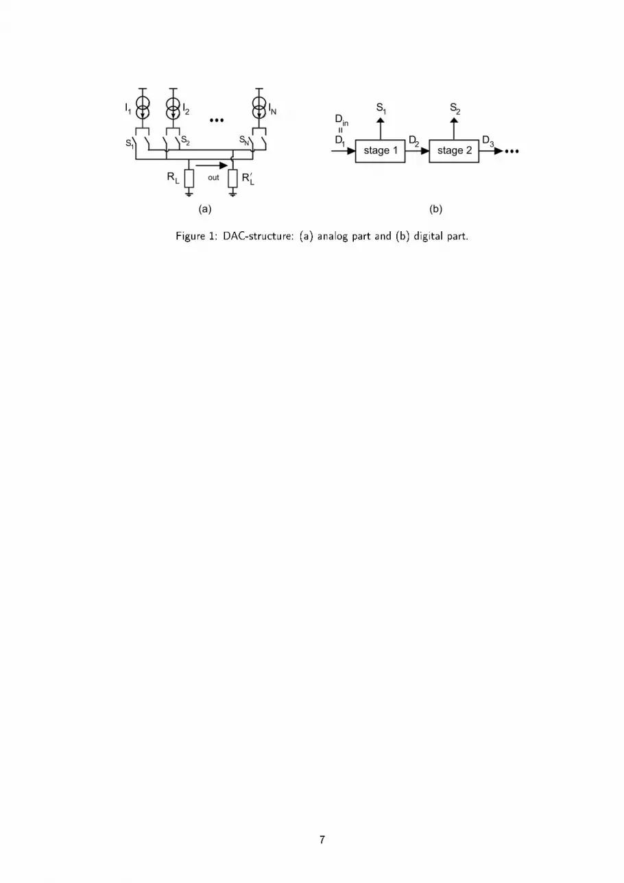
RSD Coded DAC The architecture of an RSD-DAC will be explained here starting from a
classic binary weighted DAC. A digital input word Din, which consists of N bits, needs to be
converted into an analog signal. Without loss of generality we normalize Din such that all
valid values of Din are within the interval (-1 , +1). Now, a straightforward way to perform
this operation is to use a binary weighted current-steering DAC. For this conversion N binary
weighted current sources are used. It follows that the selection signals, Sj , needed to control
the switches in the DAC, can directly be derived from the bits of the input word Din, where
−1 < Din < 1 and Sj can be 1 or −1. Depending on the value of Sj , the current Ij of
source j will �ow into one of the matched output resistors RL or R′L (Fig. 1(a)). This way,
the di�erential voltage signal, Vout produced at the output of the DAC will be proportional
to Din and equal to
Vout = RL
N∑j=1
Sj Ij
For a binary weighted DAC this can be simpli�ed to
Vout = RLI1
N∑j=1
Sj 2j−1
where I1 is the current of the smallest current cell.
[Figure 1 about here.]
Instead of using the bits of the digital word directly, the Sj can also be derived from a cascade
of selection logic stages (Fig. 1(b)). While this approach seems an unnecessary complication
for binary weighted DAC's, its generalization for RSD-DACs will prove useful in this discussion.
This way, every selection signal Sj is made in a separate stage j of the pipeline, based on the
2

input Dj ,
Sj =
1 when 0 ≤ Dj ≤ 1
−1 when − 1 ≤ Dj ≤ 0,
Here Dj denotes the input signal of stage j. The output (or input of the next stage) Dj+1
becomes
Dj+1 = 2Dj − Sj (1)
The input-output characteristic of one stage of this binary selection logic is shown in Fig. 2(a).
In order to implement an RSD-DAC now the selection signal is also allowed to be equal to 0,
and the decision rule changes into
Sj =
1 when α ≤ Dj ≤ 1
0 when − α < Dj < α
−1 when − 1 ≤ Dj ≤ −α,
where α denotes the decision level. While in most situations where RSD coding is used α
is equal to 0.25 [2], in reality the coding works for any value 0 ≤ α ≤ 0.5. This way, three
states are possible for every stage, while the output of one stage is still de�ned by (1). The
input-output characteristic is shown in Fig. 2(b).
[Figure 2 about here.]
The use of RSD coding in the selection logic implies a slight modi�cation of the normal
current-steering DAC, to handle the three-state selection signal Sj . A simple solution for this
is to implement two half-weight current sources for each RSD coded bit. The area for the
current sources is not increased by this rearrangement and it is clear that such a circuit can
deliver a di�erential current equal to 0,+Ij or −Ij to the load and thus the three RSD-states
can be created. Let us now illustrate how this coding scheme improves the performance for
signals with a high crest factor. This means that those signals contain a lot of small values
3

and very few large values. By introducing a state Sj = 0 for every stage of the RSD-DAC
and knowing that inputs generally have a mean value equal to zero, the number of switching
current sources is adjusted to the input signal level. Indeed, when an input with a small
value, e.g. α/3, is applied to the RSD-DAC, the �rst stage will output a selection signal S1
equal to 0 and a residue signal equal to 2D1. The second stage will show a selection signal
S2 which equals to 0 and an output signal equal to 4 D1, see Fig. 3. This means that the
�rst two stages that contain the largest current sources, will not be used when this signal is
converted into an analog current. This way their associated static and dynamic errors will not
be injected in the signal, only the errors of the remaining stages will be injected, but these
are a lot smaller than those of the �rst stages.
[Figure 3 about here.]
Experimental Results The concept was veri�ed through various computer simulations on
OFDM signals. In this application the performance is quanti�ed by the Missing Tone Power
Ratio (MTPR). In the simulation an improvement in MTPR of about 12 dB was obtained by
using RSD coding. Also actual experimental measurements were performed. For this purpose
the analog portion of a current steering DAC was integrated in a 0.18 µm CMOS chip with
an active area of 0.1 mm2. The intrinsic matching of the current sources was as low as
8-bit. For ease of experimentation, the digital RSD-coder was not co-integrated in the ASIC,
but instead implemented in an external FPGA. Also a digital OFDM-generator with 12-bit
resolution was implemented in the FPGA. Due to this set-up, the maximum clock frequency
was limited to 250 MHz, which is used in these measurements. The upstream band goes from
5 MHz to 15 MHz, and the downstream band from 20 MHz to 50 MHz. In the test signal,
96 carriers are used and the crest factor was 1/6. The full scale output current was set to
20 mA. The resulting output signal was connected to a spectrum analyzer for evaluation.
4
[Figure 4 about here.]
In order to evaluate the e�ectiveness of the RSD scheme the converter was tested for both
the case of RSD coding and conventional binary weighted coding, which was implemented as
well. For the RSD coding the transition levels ±α where set at −0.5 and 0.5. Fig. 4 shows
the corresponding output spectra. In the case of binary weighted coding, the MTPR equals
41 dB while the MTPR for RSD coding is 50 dB, which is an improvement of 9dB.
Conclusions In this paper, we have presented a DAC circuit which employs a �Redundant
Signed Digit� (RSD) coding scheme to drive an array of binary weighted sources. This scheme
greatly improves the performance for small signals. This way this structure is especially useful
for signals with a large crest factor such as OFDM signals. Here we measured an improvement
in MTPR of 9dB on an experimental 250 MS/s prototype which was integrated on a very
small silicon area of only 0.1mm2 of silicon area in 0.18µm CMOS.
Authors' a�liations: B. Catteau, P. Rombouts and L. Weyten, Electronics and Information
Systems Department, Ghent University, St. Pietersnieuwstraat 41, B-9000 Gent, Belgium
References
[1] W. De Wilde, N. Scantamburlo, M. Combe, J. Van Leeuwe, K. Doorakkers, Y. Mazoyer,
C. Renous, R. Petigny, A. Bonin, B. Bayracki, B. Belhi, E. Moons, and J. Sevenhans,
�Analog front end for dmt-based vdsl,� in Digest of Tech. Papers of the IEEE Int. Solid-
State Circuits Conf. 2002, vol. 1, pp. 328 �471.
[2] B. Ginetti, P. Jespers, and A. Vandemeulebroecke, �A CMOS 13-b Cyclic RSD A/D
Converter,� IEEE J. Solid-State Circuits, vol. 27, no. 7, pp. 957�965, 1992.
5

List of Figures
1 DAC-structure: (a) analog part and (b) digital part. . . . . . . . . . . . . . . 72 The input-output characteristics of a binary stage (a) and an RSD-stage (b). . 83 The RSD stages for an input with amplitude equal to α/3 . . . . . . . . . . . 94 Output spectrum for an OFDM input signal with (a) conventional binary
weighted coding and (b) RSD coding (α = 0.5). . . . . . . . . . . . . . . . . 10
6
stage 1
S1
D1
Din=
stage 2
S2
D2 D3S1S2 SN
(a)
out
I1 I2 IN
RLRL
(b)
Figure 1: DAC-structure: (a) analog part and (b) digital part.
7

S = 1jS = 1
Dj
(a) (b)
Dj+1
Dj
Dj+1
S = -1jS = 0jS = 1jS = 1 S = -1j
-1 1
-1
1
-1 1
-1
1
Figure 2: The input-output characteristics of a binary stage (a) and an RSD-stage (b).
8
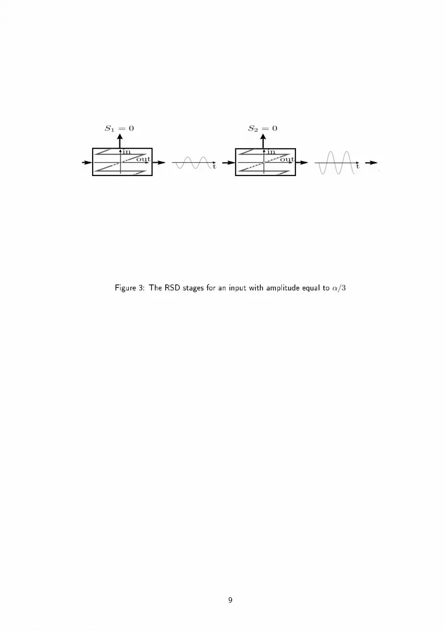
Figure 3: The RSD stages for an input with amplitude equal to α/3
9

41 d
B10 20 30 40 50 60
-80
-60
-40
-20
0
Frequency (MHz)
Out
put s
pect
rum
(dB
m)
-70
-50
-30
-10
(a)
10 20 30 40 50 60-80
-60
-40
-20
0
Frequency (MHz)
Out
put s
pect
rum
(dB
m)
50 d
B
-70
-50
-30
-10
(b)
Figure 4: Output spectrum for an OFDM input signal with (a) conventional binary weightedcoding and (b) RSD coding (α = 0.5).
10


