Embed Size (px)
Citation preview
RSC Advances
PAPER
Ope
n A
cces
s A
rtic
le. P
ublis
hed
on 2
8 M
ay 2
019.
Dow
nloa
ded
on 7
/16/
2022
8:0
1:53
PM
. T
his
artic
le is
lice
nsed
und
er a
Cre
ativ
e C
omm
ons
Attr
ibut
ion-
Non
Com
mer
cial
3.0
Unp
orte
d L
icen
ce.
View Article OnlineView Journal | View Issue
Impact of Cu do
aDepartment of Physics, PSG College of Art
Nadu, India. E-mail: nbalasundarm@gmai
0422 430 3320bDepartment of Physics, National Chung HsicNanotechnology Research Lab, Department
College, G-N Mills, Coimbatore 641 029, TadDepartment of Energy Studies, Periyar UniveInnovation and Development Center of Su
Chung Hsing University, Taichung City-4022
† Electronic supplementary information (and S2). See DOI: 10.1039/c8ra07717g
Cite this: RSC Adv., 2019, 9, 16541
Received 17th September 2018Accepted 18th April 2019
DOI: 10.1039/c8ra07717g
rsc.li/rsc-advances
This journal is © The Royal Society of C
ping on the structural,morphological and optical activity of V2O5
nanorods for photodiode fabrication and theircharacteristics†
R. Thangarasu,a B. Babu,be N. Senthil Kumar,c Mon-Shu Ho,be
O. N. Balasundaram *a and T. Elangovan d
In this paper, we report a wet chemical precipitation method used to synthesize pure and Cu-doped V2O5
nanorods with different doping concentrations (CuxV2O5 where x ¼ 3, 5 or 7 at%), followed by annealing at
600 �C and characterizations using several techniques. Indeed, a growth mechanism explaining the
morphological evolution under the experimental conditions is also proposed. The XRD patterns revealed that all
of the studied samples consist of a single V2O5 phase and are well crystallized with a preferential orientation
towards the (200) direction. The presence of intrinsic defects and internal stresses in the lattice structure of the
CuxV2O5 samples has been substantiated by detailed analysis of the XRD. Apart from the doping level, there was
an assessment of identical tiny peaks attributed to the formation of a secondary phase of CuO. SEM images
confirmed the presence of agglomerated particles on the surface; the coverage increased with Cu doping level.
XPS spectral analysis showed that Cu in the V5+ matrix exists mainly in the Cu2+ state on the surface. The
appearance of satellite peaks in the Cu 2p spectra, however, provided definitive evidence for the presence of
Cu2+ ions in these studied samples as well. Doping-induced PL quenching was observed due to the absorption
of energy from defect emission in the V5+ lattice by Cu2+ ions. We have proposed a cost-effective, less
complicated but effective way of synthesizing pure and doped samples in colloidal form, deposited by the
nebulizer spray technique on p-Si to establish junction diodes with enhanced optoelectronic properties.
1 Introduction
Semiconductor-based photodiodes have attracted considerableresearch attention for the past few decades and their optoelec-tronic devices that harvest photon-energy through distinctelectronic processes, with ultra-fast response and high respon-sivity, are of tremendous use to society in numerous applica-tions as well as optical communications, sensing, motiondetection, missile warning and biomedical imaging. All of theseapplications entail very sensitive devices with high rapidity; fastresponse time and good signal-to-noise ratio are commonlyneeded characteristics. Currently, light detection in the UV
s & Science, Coimbatore 641 014, Tamil
l.com; Fax: +91 04224303300; Tel: + 91
ng University, Taichung City 402, Taiwan
of Physics, Kongunadu Arts and Science
mil Nadu, India
ersity, Salem 636 011, Tamil Nadu, India
stainable Agriculture (IDCSA), National
7, Taiwan
ESI) available: TG/DTA studies (Fig. S1
hemistry 2019
spectral range still uses Si-based optical photodiodes due totheir sensitivity to visible and infrared radiation, intrinsically inthe UV region. On this basis, narrow bandgap semiconductors,especially Si (1.1 eV), have been commercialized for lightdetection for a long time. To avoid these disadvantages, wide-bandgap materials (such as diamond, SiC, III-nitrides andwide-bandgap II–VI materials) are under intensive study toimprove the responsivity and stability of UV photodiodes,because of their intrinsic visible-blindness. Among these,vanadium pentoxide (V2O5) is a wide direct bandgap materialdue to its sensitive UV photoresponse in the UV region. Inrecent years, much effort has been devoted to V2O5, owing to itsremarkable and unique optoelectronic properties, non-toxicity,high thermal and chemical stability, ability for use in cruelenvironments, radiation hardness, eco-friendliness, low cost,availability, etc. It is considered to be one of the most importantmetal oxide materials due to its exclusive features and becauseit is an n-type semiconductor. Metal oxides with a d0 electronconguration, such as V2O5, which contain active sites with theability to adsorb gaseous molecules and catalyze reactions ontheir surface have gained attention in past years due to theirchemical, electronic and catalytic properties and they havefound application in many technological elds. Hence, they
RSC Adv., 2019, 9, 16541–16553 | 16541
RSC Advances Paper
Ope
n A
cces
s A
rtic
le. P
ublis
hed
on 2
8 M
ay 2
019.
Dow
nloa
ded
on 7
/16/
2022
8:0
1:53
PM
. T
his
artic
le is
lice
nsed
und
er a
Cre
ativ
e C
omm
ons
Attr
ibut
ion-
Non
Com
mer
cial
3.0
Unp
orte
d L
icen
ce.
View Article Online
have emerged as the most likely to be studied, with potentialindustrial applications.1–4 A number of methods have beenimplemented for the synthesis of V2O5 nanoparticles, such ashydrothermal methods,5 solvothermal methods,6 thermaldecomposition7 and precipitation.8 Among these methods, wetchemical synthesis is promising for its control of chemicalcomponents, low cost, low processing temperature, uniformand chemically homogeneous lms, high yield and scalableprocess. Still, the properties of V2O5 can be doped with metalatoms according to the research needs via doping with variousmetal atoms to suit the specic needs and applications. Metalsubstitution can induce extreme modications in the optical,electrical and magnetic properties of V2O5 by varying its elec-tronic structure or enhancing its activity to produce somethingof real relevance. Among the major essential difficulties to beconquered is how to increase the electrical conductivity andoptical properties of metal oxides. Along with these approaches,metal oxides can be alloyed with proper elements to improvetheir optical, electrical, and magnetic performance. Hence, anextrinsic dopant (Al, Zn, Cu, W, Co and so on) is considered tobe one of the most representative dopants and it can serve asa donor in a V2O5 lattice and increase the wide bandgap engi-neering (i.e. induce defects), which will improve the electricaland optical properties of V2O5.9–13 In order to improve thematerial properties, Cu is one of the most important commondopants and it shows a good surface morphology even at highdoping levels, a moderately minor amount of deep level trapsand low memory effects. In the present work, a systematicattempt has been made to synthesize pure and CuxV2O5 nano-rods with different dopant concentrations (x ¼ 3, 5 or 7 at%) bythe wet chemical method and capping with PVP. The inuenceof Cu doping on the structural, morphological and electricalproperties of the synthesized samples was also investigated. Asan easy example and proposition, we present the colloidal formsof pure and n-CuxV2O5 deposited on p-Si substrate to form a p–njunction through the nebulizer spray technique. We plannedand fabricated a device whose recognized diode characteristicsand performance parameters were investigated throughvoltage–current measurements. The results indicate the capa-bility of the photoresponse effect to effectively enhance/optimize the performances of silicon-based optoelectronicdevices.
2 Experimental details2.1 Synthesis of pure and Cu doped V2O5 nanorods
Pure and Cu doped V2O5 nanorods were synthesized using a wetchemical route with various dopant concentrations and addi-tives. All of the chemical reagents were of analytical grade (AR)purity and were used directly without any further purication.Ammonium metavanadate [NH4VO3] was used as the vanadiumsource and copper nitrate [Cu(NO3)2] as a dopant sourcematerial. The details of the synthetic procedures for pure V2O5
nanorods are as follows: 4 mmol of ammonium metavanadatewas dissolved in 40 mL of deionized water with vigorous stirringat room temperature. Later, 10 mL of concentrated H2O2 (30%)were added into the above precursor solution with continuous
16542 | RSC Adv., 2019, 9, 16541–16553
stirring for 30 minutes to obtain a homogeneous solution andthen the solution developed a dark brown color. Aerward,0.10 g of polyvinylpyrrolidone k-30 (PVP) was added to the abovesolution and the mixture was stirred at 40 �C for 1 h. Then,HNO3 was added drop by drop to the above solution to maintainthe pH value throughout the synthesis process.14 The reactantswere introduced in this order and stirred for a fewminutes untilthe solution turned an orange-yellow color. Later, the obtainedyellow precipitates were collected, washed with deionized waterand anhydrous ethanol several times and then dried at 60 �C inair for 10 h. Finally, the above products were heated in a mufflefurnace at a 5 �C min�1 heating rate under an air atmosphere at600 �C for 1 h and cooled to room temperature. Similarly, the Cudoped V2O5 nanorods with different dopant concentrationswere also synthesized using the same procedure using thedoping source materials.
2.2 Characterization techniques
The structural characterization of the studied samples wasperformed using X-ray diffraction through a Bruker AXS D8Advance Discover X-ray diffractometer with CuKa radiation (l¼1.5406 A). The morphologies and particles sizes of the productswere investigated by scanning electronmicroscopy (JEOL-modelJSM-6390 LV), and high-resolution transmission electronmicroscopy (TECHNAI T20). The chemical composition wasanalyzed using an energy dispersive X-ray (EDS) spectroscopeattached to the SEM instrument. XPS measurements werecarried out using an SSX-100 spectrometer equipped witha focused (spot size 600 A) mono-chromatized Al Ka (anode hn¼1486.6 eV). The photoluminescence spectrum was examined byan instrument fromHoriba Jobin Yvon Fluorolog in the range of185–900 nm. The current–voltage characteristics of the devel-oped diode were examined using a source meter (Keithley 6517B) in the dark and under illumination by a calibrated solarsimulator with an irradiation intensity of 100 mW cm�2.
2.3 Possible growth mechanism of the V2O5 nanostructures
The various morphologies of the V2O5 nanostructure formationmechanism were sketched and their schematic representationsare shown in Fig. 1. As shown in the gure, the pure V2O5
nanorods assemble into a bundle-like nanorod structure.Previously, Petkov et al.15 presented a new mechanism toexplain the processes of V2O5$H2O nanobers. Recently, Weijieand his co-workers16 have explained the difficulties in thegrowth of V2O5 nanowires. They also conceived that thismechanism was appropriate for V2O5 nanorods. Therefore, themorphology of V2O5 nanorods can only be due to the effect ofthe capping agent PVP. In this case, throughout the particleformation, the monomers are adsorbed onto preferred planesand amend the tumor kinetics. Also, in the nucleation stage,growth along all preferred directions might have been retardedto produce a nanorod shaped morphology. Throughout thesynthetic process the unbroken [NH4VO3] was precipitated inthe natural solution with the concurrent formation of[H2V10O28]
4�.17,18 The basic appropriate reactions can beexpressed as follows in eqn (1)–(4),19
This journal is © The Royal Society of Chemistry 2019
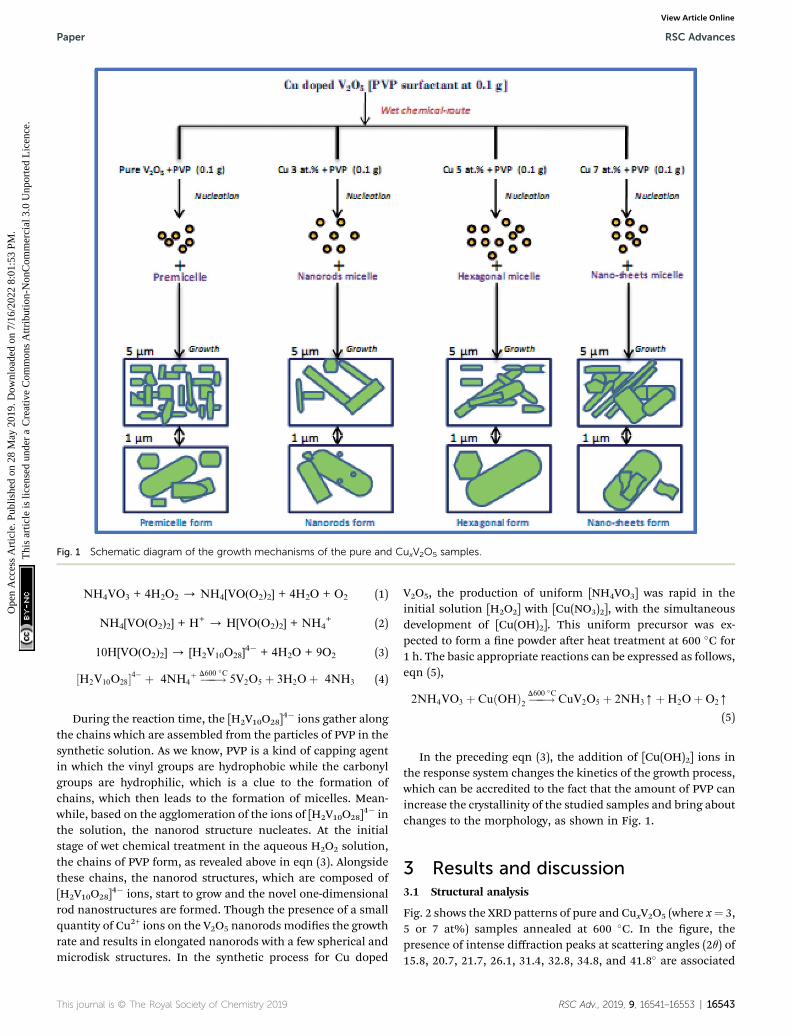
Fig. 1 Schematic diagram of the growth mechanisms of the pure and CuxV2O5 samples.
Paper RSC Advances
Ope
n A
cces
s A
rtic
le. P
ublis
hed
on 2
8 M
ay 2
019.
Dow
nloa
ded
on 7
/16/
2022
8:0
1:53
PM
. T
his
artic
le is
lice
nsed
und
er a
Cre
ativ
e C
omm
ons
Attr
ibut
ion-
Non
Com
mer
cial
3.0
Unp
orte
d L
icen
ce.
View Article Online
NH4VO3 + 4H2O2 / NH4[VO(O2)2] + 4H2O + O2 (1)
NH4[VO(O2)2] + H+ / H[VO(O2)2] + NH4+ (2)
10H[VO(O2)2] / [H2V10O28]4� + 4H2O + 9O2 (3)
½H2V10O28�4� þ 4NH4þ ���!D600 �C
5V2O5 þ 3H2Oþ 4NH3 (4)
During the reaction time, the [H2V10O28]4� ions gather along
the chains which are assembled from the particles of PVP in thesynthetic solution. As we know, PVP is a kind of capping agentin which the vinyl groups are hydrophobic while the carbonylgroups are hydrophilic, which is a clue to the formation ofchains, which then leads to the formation of micelles. Mean-while, based on the agglomeration of the ions of [H2V10O28]
4� inthe solution, the nanorod structure nucleates. At the initialstage of wet chemical treatment in the aqueous H2O2 solution,the chains of PVP form, as revealed above in eqn (3). Alongsidethese chains, the nanorod structures, which are composed of[H2V10O28]
4� ions, start to grow and the novel one-dimensionalrod nanostructures are formed. Though the presence of a smallquantity of Cu2+ ions on the V2O5 nanorods modies the growthrate and results in elongated nanorods with a few spherical andmicrodisk structures. In the synthetic process for Cu doped
This journal is © The Royal Society of Chemistry 2019
V2O5, the production of uniform [NH4VO3] was rapid in theinitial solution [H2O2] with [Cu(NO3)2], with the simultaneousdevelopment of [Cu(OH)2]. This uniform precursor was ex-pected to form a ne powder aer heat treatment at 600 �C for1 h. The basic appropriate reactions can be expressed as follows,eqn (5),
2NH4VO3 þ CuðOHÞ2 ���!D600 �CCuV2O5 þ 2NH3[þH2OþO2[
(5)
In the preceding eqn (3), the addition of [Cu(OH)2] ions inthe response system changes the kinetics of the growth process,which can be accredited to the fact that the amount of PVP canincrease the crystallinity of the studied samples and bring aboutchanges to the morphology, as shown in Fig. 1.
3 Results and discussion3.1 Structural analysis
Fig. 2 shows the XRD patterns of pure and CuxV2O5 (where x¼ 3,5 or 7 at%) samples annealed at 600 �C. In the gure, thepresence of intense diffraction peaks at scattering angles (2q) of15.8, 20.7, 21.7, 26.1, 31.4, 32.8, 34.8, and 41.8� are associated
RSC Adv., 2019, 9, 16541–16553 | 16543
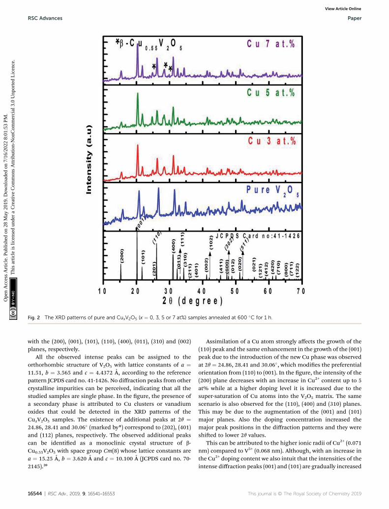
Fig. 2 The XRD patterns of pure and CuxV2O5 (x ¼ 0, 3, 5 or 7 at%) samples annealed at 600 �C for 1 h.
RSC Advances Paper
Ope
n A
cces
s A
rtic
le. P
ublis
hed
on 2
8 M
ay 2
019.
Dow
nloa
ded
on 7
/16/
2022
8:0
1:53
PM
. T
his
artic
le is
lice
nsed
und
er a
Cre
ativ
e C
omm
ons
Attr
ibut
ion-
Non
Com
mer
cial
3.0
Unp
orte
d L
icen
ce.
View Article Online
with the (200), (001), (101), (110), (400), (011), (310) and (002)planes, respectively.
All the observed intense peaks can be assigned to theorthorhombic structure of V2O5 with lattice constants of a ¼11.51, b ¼ 3.565 and c ¼ 4.4372 A, according to the referencepattern JCPDS card no. 41-1426. No diffraction peaks from othercrystalline impurities can be perceived, indicating that all thestudied samples are single phase. In the gure, the presence ofa secondary phase is attributed to Cu clusters or vanadiumoxides that could be detected in the XRD patterns of theCuxV2O5 samples. The existence of additional peaks at 2q ¼24.86, 28.41 and 30.06� (marked by*) correspond to (202), (401)and (112) planes, respectively. The observed additional peakscan be identied as a monoclinic crystal structure of b-Cu0.55V2O5 with space group Cm(8) whose lattice constants area ¼ 15.25 A, b ¼ 3.620 A and c ¼ 10.100 A (JCPDS card no. 70-2145).20
16544 | RSC Adv., 2019, 9, 16541–16553
Assimilation of a Cu atom strongly affects the growth of the(110) peak and the same enhancement in the growth of the (001)peak due to the introduction of the new Cu phase was observedat 2q ¼ 24.86, 28.41 and 30.06�, which modies the preferentialorientation from (110) to (001). In the gure, the intensity of the(200) plane decreases with an increase in Cu2+ content up to 5at% while at a higher doping level it is increased due to thesuper-saturation of Cu atoms into the V2O5 matrix. The samescenario is also observed for the (110), (400) and (310) planes.This may be due to the augmentation of the (001) and (101)major planes. Also the doping concentration increased themajor peak positions in the diffraction patterns and they wereshied to lower 2q values.
This can be attributed to the higher ionic radii of Cu2+ (0.071nm) compared to V5+ (0.068 nm). Although, with an increase inthe Cu2+ doping content we also intuit that the intensities of theintense diffraction peaks (001) and (101) are gradually increased
This journal is © The Royal Society of Chemistry 2019
Paper RSC Advances
Ope
n A
cces
s A
rtic
le. P
ublis
hed
on 2
8 M
ay 2
019.
Dow
nloa
ded
on 7
/16/
2022
8:0
1:53
PM
. T
his
artic
le is
lice
nsed
und
er a
Cre
ativ
e C
omm
ons
Attr
ibut
ion-
Non
Com
mer
cial
3.0
Unp
orte
d L
icen
ce.
View Article Online
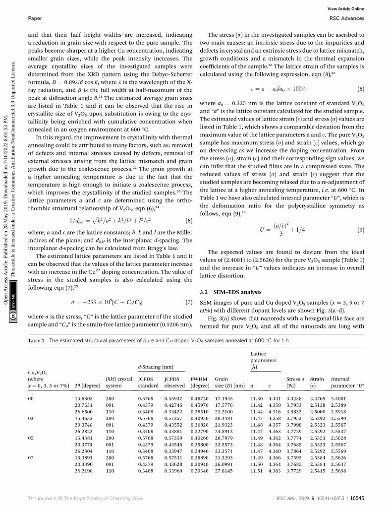
and that their half height widths are increased, indicatinga reduction in grain size with respect to the pure sample. Thepeaks become sharper at a higher Cu concentration, indicatingsmaller grain sizes, while the peak intensity increases. Theaverage crystallite sizes of the investigated samples weredetermined from the XRD pattern using the Debye–Scherrerformula, D ¼ 0.89l/b cos q, where l is the wavelength of the X-ray radiation, and b is the full width at half-maximum of thepeak at diffraction angle q.21 The estimated average grain sizesare listed in Table 1 and it can be observed that the rise incrystallite size of V2O5 upon substitution is owing to the crys-tallinity being enriched with cumulative concentration whenannealed in an oxygen environment at 600 �C.
In this regard, the improvement in crystallinity with thermalannealing could be attributed to many factors, such as: removalof defects and internal stresses caused by defects, removal ofexternal stresses arising from the lattice mismatch and graingrowth due to the coalescence process.22 The grain growth ata higher annealing temperature is due to the fact that thetemperature is high enough to initiate a coalescence process,which improves the crystallinity of the studied samples.23 Thelattice parameters a and c are determined using the ortho-rhombic structural relationship of V2O5, eqn (6),24
1=dhkl ¼ffiffiffiffiffiffiffiffiffiffiffiffiffiffiffiffiffiffiffiffiffiffiffiffiffiffiffiffiffiffiffiffiffiffiffiffiffiffiffiffiffiffiffiffih2=a2 þ k2=b2 þ l2=c2
p(6)
where, a and c are the lattice constants; h, k and l are the Millerindices of the plane; and dhkl is the interplanar d-spacing. Theinterplanar d-spacing can be calculated from Bragg's law.
The estimated lattice parameters are listed in Table 1 and itcan be observed that the values of the lattice parameter increasewith an increase in the Cu2+ doping concentration. The value ofstress in the studied samples is also calculated using thefollowing eqn (7),25
s ¼ �233 � 109[C � C0/C0] (7)
where s is the stress, “C” is the lattice parameter of the studiedsample and “C0” is the strain-free lattice parameter (0.5206 nm).
Table 1 The estimated structural parameters of pure and Cu doped V2O
CuxV2O5
(wherex ¼ 0, 3, 5 or 7%) 2q (degree)
(hkl) crystalsystem
d-Spacing (nm)
FW(de
JCPDSstandard
JCPDSobserved
00 15.8303 200 0.5768 0.55937 0.4820.7631 001 0.4379 0.42746 0.4526.6500 110 0.3408 0.33422 0.38
03 15.4633 200 0.5768 0.57257 0.4020.3748 001 0.4379 0.43552 0.3626.2822 110 0.3408 0.33881 0.32
05 15.4381 200 0.5768 0.57350 0.4020.3774 001 0.4379 0.43546 0.3526.2304 110 0.3408 0.33947 0.34
07 15.3891 200 0.5768 0.57531 0.3820.3390 001 0.4379 0.43628 0.3026.2198 110 0.3408 0.33960 0.29
This journal is © The Royal Society of Chemistry 2019
The stress (s) in the investigated samples can be ascribed totwo main causes: an intrinsic stress due to the impurities anddefects in crystal and an extrinsic stress due to lattice mismatch,growth conditions and a mismatch in the thermal expansioncoefficients of the sample.26 The lattice strain of the samples iscalculated using the following expression, eqn (8),27
3 ¼ a � a0/a0 � 100% (8)
where a0 ¼ 0.325 nm is the lattice constant of standard V2O5
and “a” is the lattice constant calculated for the studied sample.The estimated values of lattice strain (3) and stress (s) values arelisted in Table 1, which shows a comparable deviation from themaximum value of the lattice parameters a and c. The pure V2O5
sample has maximum stress (s) and strain (3) values, which goon decreasing as we increase the doping concentration. Fromthe stress (s), strain (3) and their corresponding sign values, wecan infer that the studied lms are in a compressed state. Thereduced values of stress (s) and strain (3) suggest that thestudied samples are becoming relaxed due to a re-adjustment ofthe lattice at a higher annealing temperature, i.e. at 600 �C. InTable 1 we have also calculated internal parameter “U”, which isthe deformation ratio for the polycrystalline symmetry asfollows, eqn (9),28
U ¼ ða=cÞ23
þ 1=4 (9)
The expected values are found to deviate from the idealvalues of (2.4081) to (2.5626) for the pure V2O5 sample (Table 1)and the increase in “U” values indicates an increase in overalllattice distortion.
3.2 SEM–EDS analysis
SEM images of pure and Cu doped V2O5 samples (x ¼ 3, 5 or 7at%) with different dopant levels are shown Fig. 3(a–d).
Fig. 3(a) shows that nanorods with a hexagonal-like face areformed for pure V2O5 and all of the nanorods are long with
5 samples annealed at 600 �C for 1 h
HMgree)
Grainsize (D) (nm)
Latticeparameters(A)
Stress s(Pa)
Strain(3)
Internalparameter “U”a c
720 17.1945 11.30 4.441 3.4238 2.4769 2.4081970 17.5776 11.42 4.358 3.7953 2.5138 2.5389510 21.2100 11.44 4.316 3.9832 2.5000 2.5918950 20.4481 11.47 4.358 3.7953 2.5292 2.5590820 21.9323 11.48 4.357 3.7998 2.5323 2.5567790 24.8912 11.47 4.363 3.7729 2.5292 2.5537260 20.7979 11.49 4.362 3.7774 2.5353 2.5628800 22.5573 11.48 4.364 3.7685 2.5323 2.5567940 23.3571 11.47 4.360 3.7864 2.5292 2.5569890 21.5293 11.49 4.366 3.7595 2.5384 2.5626940 26.0991 11.50 4.364 3.7685 2.5384 2.5647340 27.8145 11.51 4.363 3.7729 2.5415 2.5698
RSC Adv., 2019, 9, 16541–16553 | 16545
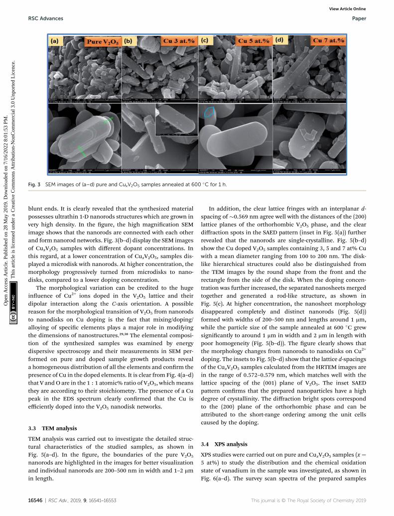
Fig. 3 SEM images of (a–d) pure and CuxV2O5 samples annealed at 600 �C for 1 h.
RSC Advances Paper
Ope
n A
cces
s A
rtic
le. P
ublis
hed
on 2
8 M
ay 2
019.
Dow
nloa
ded
on 7
/16/
2022
8:0
1:53
PM
. T
his
artic
le is
lice
nsed
und
er a
Cre
ativ
e C
omm
ons
Attr
ibut
ion-
Non
Com
mer
cial
3.0
Unp
orte
d L
icen
ce.
View Article Online
blunt ends. It is clearly revealed that the synthesized materialpossesses ultrathin 1-D nanorods structures which are grown invery high density. In the gure, the high magnication SEMimage shows that the nanorods are connected with each otherand form nanorod networks. Fig. 3(b–d) display the SEM imagesof CuxV2O5 samples with different dopant concentrations. Inthis regard, at a lower concentration of CuxV2O5, samples dis-played a microdisk with nanorods. At higher concentration, themorphology progressively turned from microdisks to nano-disks, compared to a lower doping concentration.
The morphological variation can be credited to the hugeinuence of Cu2+ ions doped in the V2O5 lattice and theirdipolar interaction along the C-axis orientation. A possiblereason for the morphological transition of V2O5 from nanorodsto nanodisks on Cu doping is the fact that mixing/doping/alloying of specic elements plays a major role in modifyingthe dimensions of nanostructures.29,30 The elemental composi-tion of the synthesized samples was examined by energydispersive spectroscopy and their measurements in SEM per-formed on pure and doped sample growth products reveala homogeneous distribution of all the elements and conrm thepresence of Cu in the doped elements. It is clear from Fig. 4(a–d)that V and O are in the 1 : 1 atomic% ratio of V2O5, whichmeansthey are according to their stoichiometry. The presence of a Cupeak in the EDS spectrum clearly conrmed that the Cu isefficiently doped into the V2O5 nanodisk networks.
3.3 TEM analysis
TEM analysis was carried out to investigate the detailed struc-tural characteristics of the studied samples, as shown inFig. 5(a–d). In the gure, the boundaries of the pure V2O5
nanorods are highlighted in the images for better visualizationand individual nanorods are 200–500 nm in width and 1–2 mmin length.
16546 | RSC Adv., 2019, 9, 16541–16553
In addition, the clear lattice fringes with an interplanar d-spacing of �0.569 nm agree well with the distances of the (200)lattice planes of the orthorhombic V2O5 phase, and the cleardiffraction spots in the SAED pattern (inset in Fig. 5(a)) furtherrevealed that the nanorods are single-crystalline. Fig. 5(b–d)show the Cu doped V2O5 samples containing 3, 5 and 7 at% Cuwith a mean diameter ranging from 100 to 200 nm. The disk-like hierarchical structures could also be distinguished fromthe TEM images by the round shape from the front and therectangle from the side of the disk. When the doping concen-tration was further increased, the separated nanosheets mergedtogether and generated a rod-like structure, as shown inFig. 5(c). At higher concentration, the nanosheet morphologydisappeared completely and distinct nanorods (Fig. 5(d))formed with widths of 200–500 nm and lengths around 1 mm,while the particle size of the sample annealed at 600 �C grewsignicantly to around 1 mm in width and 2 mm in length withpoor homogeneity (Fig. 5(b–d)). The gure clearly shows thatthe morphology changes from nanorods to nanodisks on Cu2+
doping. The insets to Fig. 5(b–d) show that the lattice d-spacingsof the CuxV2O5 samples calculated from the HRTEM images arein the range of 0.572–0.579 nm, which matches well with thelattice spacing of the (001) plane of V2O5. The inset SAEDpattern conrms that the prepared nanoparticles have a highdegree of crystallinity. The diffraction bright spots correspondto the (200) plane of the orthorhombic phase and can beattributed to the short-range ordering among the unit cellscaused by the doping.
3.4 XPS analysis
XPS studies were carried out on pure and CuxV2O5 samples (x ¼5 at%) to study the distribution and the chemical oxidationstate of vanadium in the sample was investigated, as shown inFig. 6(a–d). The survey scan spectra of the prepared samples
This journal is © The Royal Society of Chemistry 2019
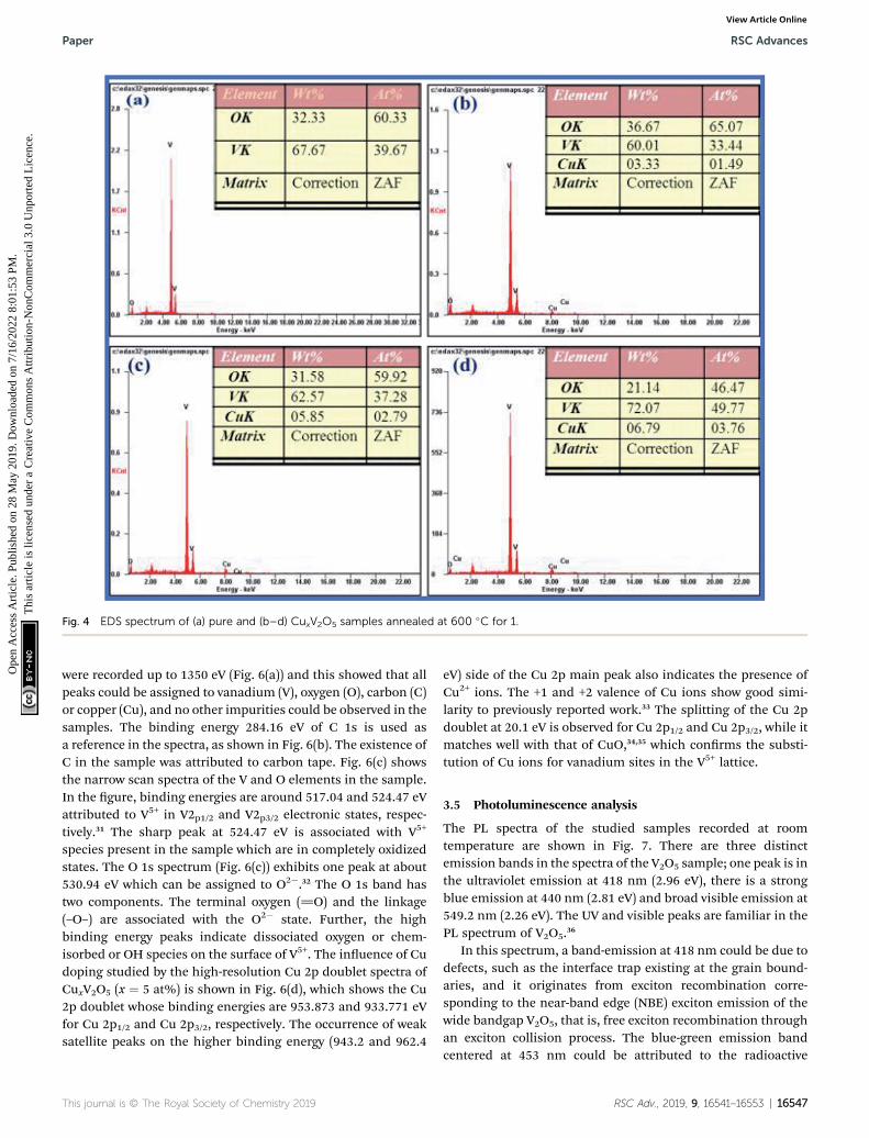
Fig. 4 EDS spectrum of (a) pure and (b–d) CuxV2O5 samples annealed at 600 �C for 1.
Paper RSC Advances
Ope
n A
cces
s A
rtic
le. P
ublis
hed
on 2
8 M
ay 2
019.
Dow
nloa
ded
on 7
/16/
2022
8:0
1:53
PM
. T
his
artic
le is
lice
nsed
und
er a
Cre
ativ
e C
omm
ons
Attr
ibut
ion-
Non
Com
mer
cial
3.0
Unp
orte
d L
icen
ce.
View Article Online
were recorded up to 1350 eV (Fig. 6(a)) and this showed that allpeaks could be assigned to vanadium (V), oxygen (O), carbon (C)or copper (Cu), and no other impurities could be observed in thesamples. The binding energy 284.16 eV of C 1s is used asa reference in the spectra, as shown in Fig. 6(b). The existence ofC in the sample was attributed to carbon tape. Fig. 6(c) showsthe narrow scan spectra of the V and O elements in the sample.In the gure, binding energies are around 517.04 and 524.47 eVattributed to V5+ in V2p1/2 and V2p3/2 electronic states, respec-tively.31 The sharp peak at 524.47 eV is associated with V5+
species present in the sample which are in completely oxidizedstates. The O 1s spectrum (Fig. 6(c)) exhibits one peak at about530.94 eV which can be assigned to O2�.32 The O 1s band hastwo components. The terminal oxygen (]O) and the linkage(–O–) are associated with the O2� state. Further, the highbinding energy peaks indicate dissociated oxygen or chem-isorbed or OH species on the surface of V5+. The inuence of Cudoping studied by the high-resolution Cu 2p doublet spectra ofCuxV2O5 (x ¼ 5 at%) is shown in Fig. 6(d), which shows the Cu2p doublet whose binding energies are 953.873 and 933.771 eVfor Cu 2p1/2 and Cu 2p3/2, respectively. The occurrence of weaksatellite peaks on the higher binding energy (943.2 and 962.4
This journal is © The Royal Society of Chemistry 2019
eV) side of the Cu 2p main peak also indicates the presence ofCu2+ ions. The +1 and +2 valence of Cu ions show good simi-larity to previously reported work.33 The splitting of the Cu 2pdoublet at 20.1 eV is observed for Cu 2p1/2 and Cu 2p3/2, while itmatches well with that of CuO,34,35 which conrms the substi-tution of Cu ions for vanadium sites in the V5+ lattice.
3.5 Photoluminescence analysis
The PL spectra of the studied samples recorded at roomtemperature are shown in Fig. 7. There are three distinctemission bands in the spectra of the V2O5 sample; one peak is inthe ultraviolet emission at 418 nm (2.96 eV), there is a strongblue emission at 440 nm (2.81 eV) and broad visible emission at549.2 nm (2.26 eV). The UV and visible peaks are familiar in thePL spectrum of V2O5.36
In this spectrum, a band-emission at 418 nm could be due todefects, such as the interface trap existing at the grain bound-aries, and it originates from exciton recombination corre-sponding to the near-band edge (NBE) exciton emission of thewide bandgap V2O5, that is, free exciton recombination throughan exciton collision process. The blue-green emission bandcentered at 453 nm could be attributed to the radioactive
RSC Adv., 2019, 9, 16541–16553 | 16547
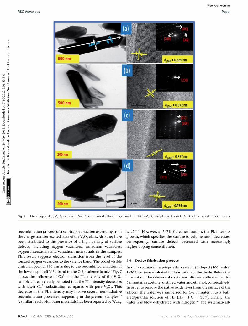
Fig. 5 TEM images of (a) V2O5 with inset SAED pattern and lattice fringes and (b–d) CuxV2O5 samples with inset SAED patterns and lattice fringes.
RSC Advances Paper
Ope
n A
cces
s A
rtic
le. P
ublis
hed
on 2
8 M
ay 2
019.
Dow
nloa
ded
on 7
/16/
2022
8:0
1:53
PM
. T
his
artic
le is
lice
nsed
und
er a
Cre
ativ
e C
omm
ons
Attr
ibut
ion-
Non
Com
mer
cial
3.0
Unp
orte
d L
icen
ce.
View Article Online
recombination process of a self-trapped exciton ascending fromthe charge transfer excited state of the V2O5 class. Also they havebeen attributed to the presence of a high density of surfacedefects, including oxygen vacancies, vanadium vacancies,oxygen interstitials and vanadium interstitials in the samples.This result suggests electron transition from the level of theionized oxygen vacancies to the valence band. The broad visibleemission peak at 550 nm is due to the recombined emission ofthe lowest split-off V 3d band to the O 2p valence band.37 Fig. 7shows the inuence of Cu2+ on the PL intensity of the V2O5
samples. It can clearly be noted that the PL intensity decreaseswith lower Cu2+ substitution compared with pure V2O5. Thisdecrease in the PL intensity may involve several non-radiativerecombination processes happening in the present samples.38
A similar result with other materials has been reported by Wang
16548 | RSC Adv., 2019, 9, 16541–16553
et al.39–41 However, at 5–7% Cu concentration, the PL intensitygrowth, which species the surface to volume ratio, decreases;consequently, surface defects decreased with increasinglyhigher doping concentration.
3.6 Device fabrication process
In our experiment, a p-type silicon wafer (B-doped (100) wafer,1–30U cm) was exploited for fabrication of the diode. Before thefabrication, the silicon substrate was ultrasonically cleaned for5 minutes in acetone, distilled water and ethanol, consecutively.In order to remove the native oxide layer from the surface of thesilicon, the wafer was immersed for 1–2 minutes into a buff-ered/piranha solution of HF (HF : H2O ¼ 1 : 7). Finally, thewafer was blow dehydrated with nitrogen.42 The systematically
This journal is © The Royal Society of Chemistry 2019
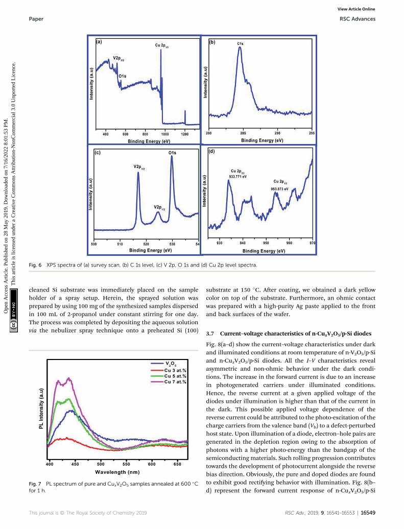
Fig. 6 XPS spectra of (a) survey scan, (b) C 1s level, (c) V 2p, O 1s and (d) Cu 2p level spectra.
Paper RSC Advances
Ope
n A
cces
s A
rtic
le. P
ublis
hed
on 2
8 M
ay 2
019.
Dow
nloa
ded
on 7
/16/
2022
8:0
1:53
PM
. T
his
artic
le is
lice
nsed
und
er a
Cre
ativ
e C
omm
ons
Attr
ibut
ion-
Non
Com
mer
cial
3.0
Unp
orte
d L
icen
ce.
View Article Online
cleaned Si substrate was immediately placed on the sampleholder of a spray setup. Herein, the sprayed solution wasprepared by using 100 mg of the synthesized samples dispersedin 100 mL of 2-propanol under constant stirring for one day.The process was completed by depositing the aqueous solutionvia the nebulizer spray technique onto a preheated Si (100)
Fig. 7 PL spectrum of pure and CuxV2O5 samples annealed at 600 �Cfor 1 h.
This journal is © The Royal Society of Chemistry 2019
substrate at 150 �C. Aer coating, we obtained a dark yellowcolor on top of the substrate. Furthermore, an ohmic contactwas prepared with a high-purity Ag paste applied to the frontand back surfaces of the wafer.
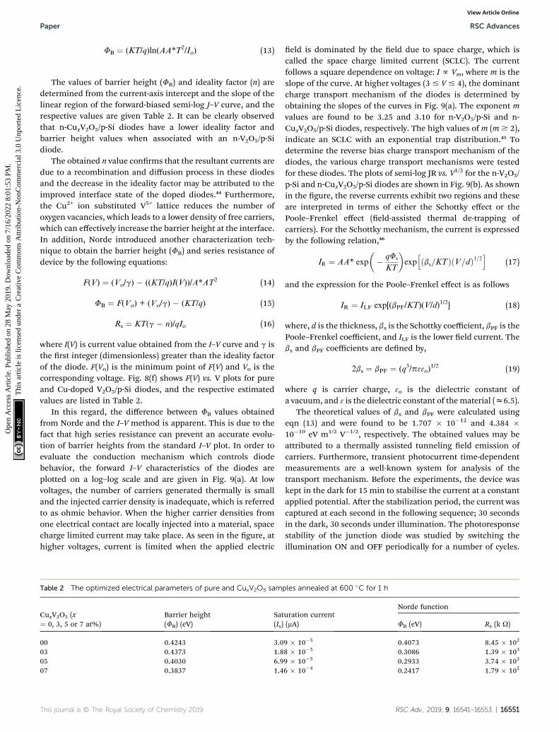
3.7 Current–voltage characteristics of n-CuxV2O5/p-Si diodes
Fig. 8(a–d) show the current–voltage characteristics under darkand illuminated conditions at room temperature of n-V2O5/p-Siand n-CuxV2O5/p-Si diodes. All the I–V characteristics revealasymmetric and non-ohmic behavior under the dark condi-tions. The increase in the forward current is due to an increasein photogenerated carriers under illuminated conditions.Hence, the reverse current at a given applied voltage of thediodes under illumination is higher than that of the current inthe dark. This possible applied voltage dependence of thereverse current could be attributed to the photo-excitation of thecharge carriers from the valence band (Vb) to a defect-perturbedhost state. Upon illumination of a diode, electron–hole pairs aregenerated in the depletion region owing to the absorption ofphotons with a higher photo-energy than the bandgap of thesemiconductingmaterials. Such rolling progression contributestowards the development of photocurrent alongside the reversebias direction. Obviously, the pure and doped diodes are foundto exhibit good rectifying behavior with illumination. Fig. 8(b–d) represent the forward current response of n-CuxV2O5/p-Si
RSC Adv., 2019, 9, 16541–16553 | 16549
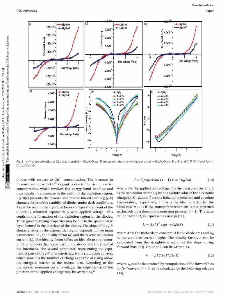
Fig. 8 I–V characteristics of (a) pure, (c and d) n-CuxV2O5/p-Si, (e) current density–voltage plots of n-CuxV2O5/p-Si p-Si and (f) F(V)–V plot for n-CuxV2O5/p-Si.
RSC Advances Paper
Ope
n A
cces
s A
rtic
le. P
ublis
hed
on 2
8 M
ay 2
019.
Dow
nloa
ded
on 7
/16/
2022
8:0
1:53
PM
. T
his
artic
le is
lice
nsed
und
er a
Cre
ativ
e C
omm
ons
Attr
ibut
ion-
Non
Com
mer
cial
3.0
Unp
orte
d L
icen
ce.
View Article Online
diodes with respect to Cu2+ concentration. The increase inforward current with Cu2+ dopant is due to the rise in carrierconcentration, which involves the energy band bending andthus results in a decrease in the width of the depletion region.Fig. 8(e) presents the forward and reverse biased semi-log (J–V)characteristics of the established diodes under dark conditions.As can be seen in the gure, at lower voltages the current of thediodes is reformed exponentially with applied voltage. Thisconrms the formation of the depletion region in the diodes.These good rectifying properties may be due to the space chargelayer formed in the interface of the diodes. The slope of the J–Vcharacteristics in the exponential region depends on two mainparameters: i.e., an ideality factor (n) and the reverse saturationcurrent (Is). The ideality factor offers an idea about the recom-bination process that takes place in the device and the shape ofthe interfaces. The second parameter, representing the expo-nential part of the J–V characteristics, is the saturation current,which provides the number of charges capable of rising abovethe energetic barrier in the reverse bias. According to thethermionic emission current–voltage, the dependence of thejunction of the applied voltage may be written as,43
16550 | RSC Adv., 2019, 9, 16541–16553
I ¼ Is[exp(qV/nKT) � 1](V $ 3KBT/q) (10)
where V is the applied bias voltage, I is the measured current, Isis the saturation current, q is the absolute value of the electroniccharge (in C), KB and T are the Boltzmann constant and absolutetemperature, respectively, and n is the ideality factor (in theideal case n ¼ 1; if the transport mechanism is not governedexclusively by a thermionic emission process, n > 1). The satu-ration current Is is expressed as in eqn (11),
Is ¼ AA*T2 exp(�qFB/KT) (11)
where A* is the Richardson constant, A is the diode area and FB
is the zero-bias barrier height. The ideality factor, n can becalculated from the straight-line region of the slope duringforward bias ln(I)–V plot and can be written as,
n ¼ (q/KT)(dV/d(ln I)) (12)
where, Io can be determined by extrapolation of the forward biasln(I)–V curve to V ¼ 0. FB is calculated by the following relation(13),
This journal is © The Royal Society of Chemistry 2019
Paper RSC Advances
Ope
n A
cces
s A
rtic
le. P
ublis
hed
on 2
8 M
ay 2
019.
Dow
nloa
ded
on 7
/16/
2022
8:0
1:53
PM
. T
his
artic
le is
lice
nsed
und
er a
Cre
ativ
e C
omm
ons
Attr
ibut
ion-
Non
Com
mer
cial
3.0
Unp
orte
d L
icen
ce.
View Article Online
FB ¼ (KT/q)ln(AA*T2/Io) (13)
The values of barrier height (FB) and ideality factor (n) aredetermined from the current-axis intercept and the slope of thelinear region of the forward-biased semi-log J–V curve, and therespective values are given Table 2. It can be clearly observedthat n-CuxV2O5/p-Si diodes have a lower ideality factor andbarrier height values when associated with an n-V2O5/p-Sidiode.
The obtained n value conrms that the resultant currents aredue to a recombination and diffusion process in these diodesand the decrease in the ideality factor may be attributed to theimproved interface state of the doped diodes.44 Furthermore,the Cu2+ ion substituted V5+ lattice reduces the number ofoxygen vacancies, which leads to a lower density of free carriers,which can effectively increase the barrier height at the interface.In addition, Norde introduced another characterization tech-nique to obtain the barrier height (FB) and series resistance ofdevice by the following equations:
F(V) ¼ (Vo/g) � ((KT/q)I(V))/A*AT2 (14)
FB ¼ F(Vo) + (Vo/g) � (KT/q) (15)
Rs ¼ KT(g � n)/qIo (16)
where I(V) is current value obtained from the I–V curve and g isthe rst integer (dimensionless) greater than the ideality factorof the diode. F(Vo) is the minimum point of F(V) and Vo is thecorresponding voltage. Fig. 8(f) shows F(V) vs. V plots for pureand Cu-doped V2O5/p-Si diodes, and the respective estimatedvalues are listed in Table 2.
In this regard, the difference between FB values obtainedfrom Norde and the I–V method is apparent. This is due to thefact that high series resistance can prevent an accurate evolu-tion of barrier heights from the standard I–V plot. In order toevaluate the conduction mechanism which controls diodebehavior, the forward I–V characteristics of the diodes areplotted on a log–log scale and are given in Fig. 9(a). At lowvoltages, the number of carriers generated thermally is smalland the injected carrier density is inadequate, which is referredto as ohmic behavior. When the higher carrier densities fromone electrical contact are locally injected into a material, spacecharge limited current may take place. As seen in the gure, athigher voltages, current is limited when the applied electric
Table 2 The optimized electrical parameters of pure and CuxV2O5 sam
CuxV2O5 (x¼ 0, 3, 5 or 7 at%)
Barrier height(FB) (eV)
Sat(Is)
00 0.4243 3.003 0.4373 1.805 0.4030 6.907 0.3837 1.4
This journal is © The Royal Society of Chemistry 2019
eld is dominated by the eld due to space charge, which iscalled the space charge limited current (SCLC). The currentfollows a square dependence on voltage: I f Vm, where m is theslope of the curve. At higher voltages (3 # V # 4), the dominantcharge transport mechanism of the diodes is determined byobtaining the slopes of the curves in Fig. 9(a). The exponent mvalues are found to be 3.25 and 3.10 for n-V2O5/p-Si and n-CuxV2O5/p-Si diodes, respectively. The high values of m (m$ 2),indicate an SCLC with an exponential trap distribution.45 Todetermine the reverse bias charge transport mechanism of thediodes, the various charge transport mechanisms were testedfor these diodes. The plots of semi-log JR vs. V1/2 for the n-V2O5/p-Si and n-CuxV2O5/p-Si diodes are shown in Fig. 9(b). As shownin the gure, the reverse currents exhibit two regions and theseare interpreted in terms of either the Schottky effect or thePoole–Frenkel effect (eld-assisted thermal de-trapping ofcarriers). For the Schottky mechanism, the current is expressedby the following relation,46
IR ¼ AA* exp
�� qFs
KT
�exp
hðbs=KTÞðV=dÞ1=2
i(17)
and the expression for the Poole–Frenkel effect is as follows
IR ¼ ILF exp[(bPF/KT)(V/d)1/2] (18)
where, d is the thickness, bs is the Schottky coefficient, bPF is thePoole–Frenkel coefficient, and ILF is the lower eld current. Thebs and bPF coefficients are dened by,
2bs ¼ bPF ¼ (q3/p33o)1/2 (19)
where q is carrier charge, 3o is the dielectric constant ofa vacuum, and 3 is the dielectric constant of thematerial (z6.5).
The theoretical values of bs and bPF were calculated usingeqn (13) and were found to be 1.707 � 10�12 and 4.384 �10�10 eV m1/2 V�1/2, respectively. The obtained values may beattributed to a thermally assisted tunneling eld emission ofcarriers. Furthermore, transient photocurrent time-dependentmeasurements are a well-known system for analysis of thetransport mechanism. Before the experiments, the device waskept in the dark for 15 min to stabilise the current at a constantapplied potential. Aer the stabilization period, the current wascaptured at each second in the following sequence; 30 secondsin the dark, 30 seconds under illumination. The photoresponsestability of the junction diode was studied by switching theillumination ON and OFF periodically for a number of cycles.
ples annealed at 600 �C for 1 h
uration current(mA)
Norde function
FB (eV) Rs (k U)
9 � 10�5 0.4073 8.45 � 102
8 � 10�5 0.3086 1.39 � 103
9 � 10�5 0.2933 3.74 � 102
6 � 10�4 0.2417 1.79 � 102
RSC Adv., 2019, 9, 16541–16553 | 16551
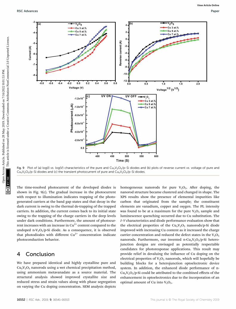
Fig. 9 Plot of (a) log(I) vs. log(V) characteristics of the pure and CuxV2O5/p-Si diodes and (b) plots of reverse current vs. voltage of pure andCuxV2O5/p-Si diodes and (c) the transient photocurrent of pure and CuxV2O5/p-Si diodes.
RSC Advances Paper
Ope
n A
cces
s A
rtic
le. P
ublis
hed
on 2
8 M
ay 2
019.
Dow
nloa
ded
on 7
/16/
2022
8:0
1:53
PM
. T
his
artic
le is
lice
nsed
und
er a
Cre
ativ
e C
omm
ons
Attr
ibut
ion-
Non
Com
mer
cial
3.0
Unp
orte
d L
icen
ce.
View Article Online
The time-resolved photocurrent of the developed diodes isshown in Fig. 9(c). The gradual increase in the photocurrentwith respect to illumination indicates trapping of the photo-generated carriers at the band gap states and that decay in thedark current is owing to the thermal de-trapping of the trappedcarriers. In addition, the current comes back to its initial stateowing to the trapping of the charge carriers in the deep levelsunder dark conditions. Furthermore, the amount of photocur-rent increases with an increase in Cu2+ content compared to theundoped n-V2O5/p-Si diode. As a consequence, it is observedthat photodiodes with different Cu2+ concentration indicatephotoconduction behavior.
4 Conclusion
We have prepared identical and highly crystalline pure andCuxV2O5 nanorods using a wet chemical precipitation method,using ammonium metavanadate as a source material. Thestructural analysis showed improved crystallite size andreduced stress and strain values along with phase segregationon varying the Cu doping concentration. SEM analysis depicts
16552 | RSC Adv., 2019, 9, 16541–16553
homogeneous nanorods for pure V2O5. Aer doping, thenanorod structure became clustered and changed in shape. TheXPS results show the presence of elemental impurities likecarbon that originated from the sample; the constituentelements are vanadium, copper and oxygen. The PL intensitywas found to be at a maximum for the pure V2O5 sample andluminescence quenching occurred due to Cu substitution. TheI–V characteristics and diode performance evaluation show thatthe electrical properties of the CuxV2O5 nanorods/p-Si diodeimproved with increasing Cu content as it increased the chargecarrier concentration and reduced the defect states in the V2O5
nanorods. Furthermore, our invented n-CuxV2O5/p-Si hetero-junction designs are envisaged as potentially respectablecandidates for photoresponse applications. This result mayprovide relief in devaluing the inuence of Cu doping on theelectrical properties of V2O5 nanorods, which will hopefully bebuilding blocks for a heterojunction optoelectronic devicesystem. In addition, the enhanced diode performance of n-CuxV2O5/p-Si could be attributed to the combined effects of theenhancement in optoelectronics due to the incorporation of anoptimal amount of Cu into V2O5.
This journal is © The Royal Society of Chemistry 2019
Paper RSC Advances
Ope
n A
cces
s A
rtic
le. P
ublis
hed
on 2
8 M
ay 2
019.
Dow
nloa
ded
on 7
/16/
2022
8:0
1:53
PM
. T
his
artic
le is
lice
nsed
und
er a
Cre
ativ
e C
omm
ons
Attr
ibut
ion-
Non
Com
mer
cial
3.0
Unp
orte
d L
icen
ce.
View Article Online
Conflicts of interest
There are no conicts to declare.
References
1 Y. Zhang, J. Zheng, Q. Wang, T. Hu and C. Meng, RSC Adv.,2016, 6, 93741.
2 R. Wang, S. Yang, R. Deng, W. Chen, Y. Liu, H. Zhang andG. S. Zakharova, RSC Adv., 2015, 5, 41050.
3 S. Raque, S. M. Abdullah, W. E. Mahmoud, A. A. Al-Ghamdiand K. Sulaiman, RSC Adv., 2016, 6, 50043.
4 X. Liu, J. Zeng, H. Yang, K. Zhou and P. Deng, RSC Adv., 2018,8, 4014.
5 J. Wu, Y. Zhang, Y. He, C. Liu, W. Guolt and S. Ruan, J.Nanosci. Nanotechnol., 2014, 14, 4214.
6 N. Wang, Y. Zhang, T. Hu, Y. Zhao and C. Meng, Curr. Appl.Phys., 2015, 15, 493.
7 X. Zhang, M. Wu, S. Gao, Y. Xu, X. Cheng, H. Zhao andL. Huo, Mater. Res. Bull., 2014, 60, 659.
8 J. Huang, X. Qiao, Z. Xu, L. Cao, H. Ouyang, J. Li andR. Wang, Electrochim. Acta, 2016, 191, 158.
9 S. Zhan, Y. Wei, X. Bie, C. Wang, F. Du, G. Chen and F. Hu, J.Alloy. Comp., 2010, 502, 92.
10 R. Abaira, T. Dammak, A. Matoussi and A. Younes,Superlattice. Microst., 2016, 91, 365.
11 D. Zhu, H. Liu, L. Lv, Y. D. Yao andW. Z. Yang, Scripta Mater.,2008, 59, 642.
12 Q. Song, H. Pang, W. Gong, G. Ning, Y. Zhang, X. Cheng andL. Yuan, Mater. Lett., 2015, 161, 244.
13 R. Suresh, K. Giribabu, R. Manigandan, S. Munusamy,S. Praveen Kumar, S. Muthamizh, A. Stephen andV. Narayanan, J. Alloy. Comp., 2014, 598, 151.
14 M. Zeng, H. Yin and K. Yu, Chem. Eng. J., 2012, 188, 64.15 V. Petkov, P. N. Trikalitis, E. S. Bozin, S. J. L. Billinge, T. Vogt
and M. G. Kanatzidis, J. Am. Chem. Soc., 2002, 124, 10157.16 Y. Weijie, W. Jinxing, G. Zhong ping, Z. Wen, G. Weiwei and
L. Liyang, Ceram. Int., 2013, 39, 2639.17 B. Alonso and J. Livage, J. Solid State Chem., 1999, 148, 16.18 C. J. Fontenot, J. W. Wiench, M. Pruski and G. L. Schrader, J.
Phys. Chem. B, 2000, 104, 11622.19 T. C. Gujjarahalli, C. Pallellappa, A. Siddaramanan and
L. Jacques, Inorg. Chem., 2011, 50, 7421.20 J. Galy, D. Lavaud, A. Casalot and P. Hagenmuller, J. Solid
State Chem., 1970, 2, 531.21 Y. Zhang, J. Zheng, Y. Zhao, T. Hu, Z. Gao and C. Meng, Appl.
Surf. Sci., 2016, 377, 385.22 X. L. Zhang, Cryst. Growth Des., 2008, 8, 2609.
This journal is © The Royal Society of Chemistry 2019
23 V. Kumar, R. G. Singh, F. Singh and L. P. Purohit, J. Alloy.Comp., 2012, 544, 120.
24 N. Senthil kumar, M. Sethu Raman, J. Chandrasekaran,R. Priya, M. Chavali and R. Suresh, Mater. Sci. Semicond.Process., 2016, 41, 497.
25 K. Joshi, M. Rawat, S. K. Gautam, R. G. Singh, R. C. Ramolaand F. Singh, J. Alloys Compd., 2016, 680, 252.
26 M. Chen, Z. L. Pei, C. Sun, L. S. Wen and X. Wang, J. Cryst.Growth, 2000, 220, 254.
27 R. Ghosh, D. Basak and S. Fujihara, J. Appl. Phys., 2004, 96,2689.
28 H. Schulz and K. H. Thiemann, Solid State Commun., 1979,32, 783.
29 M. Hafeez, U. Manzoor, A. S. Bhatti, B. Karnayar andS. I. Shah, J. Appl. Phys., 2012, 111, 024313.
30 H. J. Fan, B. Fuhrmann, R. Scholz, C. Himcinschi, A. Berger,H. Leipner, A. Dadgar, A. Krost, S. H. Christiansen, U. Goseleand M. Zacharias, Nanotechnology, 2006, 17, 231.
31 C. W. Zou, Y. F. Rao, A. Alyamani, W. Chu, M. J. Chen,D. A. Patterson, E. A. C. Emanuelsson and W. Gao,Langmuir, 2010, 26, 11615.
32 Y. S. Hu, X. Liu, J. O. Muller, R. Schlogl, J. Maier and D. S. Su,Angew. Chem., Int. Ed., 2009, 48, 210.
33 D. Chakraborti, G. R. Trhchy, J. T. Prater and J. Narayan, J.Phys. D: Appl. Phys., 2007, 40, 7606.
34 G. Schon, Surf. Sci., 1973, 35, 96.35 I. Nakai, Y. Sugitani, K. Nagashima and Y. Niwa, J. Inorg.
Nucl. Chem., 1978, 40, 789.36 K. Karthika and K. Ravichandran, J. Mater. Sci. Technol.,
2015, 31, 1111.37 B. X. Lin, Z. X. Fu and Y. B. Jia, Appl. Phys. Lett., 2001, 79, 943.38 K. Dutta and R. J. Nelson, J. Appl. Phys., 1982, 53, 74.39 X. B. Wang, C. Song, K. W. Geng, F. Zeng and F. Pan, Appl.
Surf. Sci., 2007, 253, 6905.40 M. Anpo, S. G. Zhang, S. Higashimoto, M. Matsuoka and
H. Yamashita, J. Phys. Chem. B, 1999, 103, 9295.41 N. V. Hullavarad, S. S. Hullavarad and P. C. Karulkar, J.
Electrochem. Soc., 2008, 155, K84.42 E. H. Rhoderick and R. H. Williams, Metal-Semiconductor
Contacts, Clarendon, Oxford, 2nd edn, 1988, p. 252.43 P. Klason, M. M. Rahman, Q.-H. Hu, O. Nur, R. Turan and
M. Willander, Microelectron. J., 2009, 40, 706.44 H. M. Zhang and W. C. H. Choy, IEEE Trans. Electron Devices,
2008, 55, 2517.45 S. Aydogan, K. Çınar, H. Asıl, C. Coskun and A. Turut, J.
Alloys Compd., 2009, 476, 913.46 J. H. Evans-Freeman, M. M. El-Nahass, A. A. M. Farag and
A. Elhaji, Microelectron. Eng., 2011, 88, 3353.
RSC Adv., 2019, 9, 16541–16553 | 16553


![Computational studies of Cu(II)[peptide] binding motifs: Cu[HGGG] and Cu[HG] as models for Cu(II) binding to the prion protein octarepeat region](https://img.dokumen.tips/doc/110x75/635d3a56a3fa66b45c0e4b12/computational-studies-of-cuiipeptide-binding-motifs-cuhggg-and-cuhg-as.jpg)


