Embed Size (px)
Citation preview
[email protected], [email protected], [email protected],
Abstract— Enhancement of conversion efficiency is the principle
object in the photovoltaic technology of solar cells. III-V
semiconductors, InGaN alloy are very promising candidates for
solar cells. InGaN alloy facilitates the ability to tune the
band gap for solar energy conversion. In this work, we have
theoretically studied and evaluated InGaN based QW and QD
solar cells and InGaN based p-n, p-i-n solar cells
respectively and compared the performance with various
parameters for achieving high efficiency. Short circuit
current density, open circuit voltage and efficiency are
calculated with the dependencies of band gap energy. The
efficiency is found to be 46.38% for InGaN based QW solar
cell whereas for InGaN based p-n and p-i-n solar cell
efficiency is found to be 24.76% and 27.88% . The
calculations show that the inclusion of the QDs in the
intrinsic region does indeed enhance short circuit current
without signi cant losses in the open circuit voltage andfi
result signi cantly improved cell efficiency. In comparison offi
High Efficiency InGaN Based QuantumWell & Quantum Dot Solar Cell
Md. Abu Shahab Mollah, Md. Liton Hossain, Md. Imtiaz Islam, AbuFarzan Mitul
InGaN based p-n, p-i-n solar cell and InGaN based MQW, QD
solar cell implies that InGaN based QD solar cell offers
the highest efficiency.
Index Terms — conversion efficiency, fill factor, InGaN, photovoltaic, QWSC,Quantum Well, Quantum Dot.
I. INTRODUCTIONConversion efficiency enhancement is the main job in the photovoltaic
technology of solar cells. Recently several design schemes have been
proposed to enhance the power conversion efficiency of photovoltaic
devices. Using two or more p – n solar cell junctions, tandem cells
made of different semiconductors, a multi heterojunctions design
yields a better match to the solar spectrum than a single-junction
cell and may provide the efficiency of conversion greater than 50%
[1]. One of the methodologies is to make the solar cell absorb as much
as possible of the solar spectrum. The InGaN alloy is direct band gap
material and its band gap covers most of the solar spectrum, from 0.65
to 3.4 eV. Moreover, its high absorption coefficient at the band edge
makes it absorb most of the incident light at a few hundred
nanometres, which is beneficial to reduce the thickness of the device
[2]. It also exhibits high mobility, saturation velocity and strong
tolerance of radiation [3]. However, many enthusiastic researchers
have analyzed with different material to increase the conversion
efficiency of quantum well solar cell. Here, for convenience some
analyses are mentioned one by one. V. Aroutiounian, S. Petrosyan [1]
reported that the projected short-circuit current density for "3-step"
InGaAs/GaAs PM-MQW solar cell is Jsc = 24.66 mA/cm2, and AM1.5
conversion efficiency amounts to q = 18.27%. In reference [4], optimal
barrier thickness of 28 nm was calculated. All these strain-balanced
multi quantum well stacks were incorporated into a state-of-the-art
GaAs single-junction solar cell with an AM0 efficiency of 22.4 %.
Francis K. Rault, Ahmad Zahedi [5] showed QWSC design efficiencies
ranging 23–29% with a discrepancy of ±1:5% between presented and
existing models. Rubin Liu1, Chaogang Lou, Wei Gao, Shuai Wang, Qiang
Sun [6], showed that the triple junction solar cells with the multi-
quantum wells can reach the conversion efficiency of 30.89% (AM0),
higher than that of control cells. G. J. Lin, K. Y. Lai [7] found that
the 1.1-μm-long NRAs result in the enhanced conversion efficiency by
up to ∼ 36% due to the improved optical transmission. Md. Sherajul
Islam, Md. Shahid Iqbal [8], found the highest efficiency for InGaN
based QW cell and that was 40.2%.
In addition, many researchers have analyzed with different material to
increase the conversion efficiency of quantum dot solar cell. Here,
some analyses are also mentioned one by one. G.Kumar, S.M.Mahajan [9]
reported that simulations performed with multi-sized quantum dots
doped inside Silicon, Gallium Arsenide, and Titanium dioxide
substrates showed a potential improvement in the power conversion
efficiencies of up to 22.35 %, 12.41%, and 13.5% as compared to 15 %,
6 %, and 1.7 % respectively (with single size quantum dot doping).
In this study, we design and quantum well and quantum dot
heterojunctions solar cells with even band gap energy and number of
wells and compare their efficiency with InGaN based p-n and p-i-n
heterojunctions solar cells as well as quantum well and quantum dot
solar cell proposed by others. The large short circuit current, Open
circuit voltage, fill factor and wide spectral response range of the
proposed semiconductor devices suggests the high potential of InGaN
based heterojunctions solar cells.
II. MODEL FORMULATION
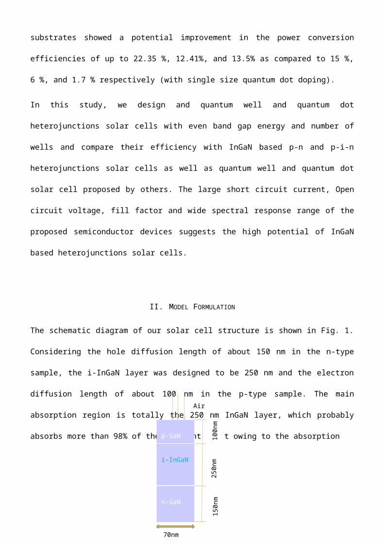
The schematic diagram of our solar cell structure is shown in Fig. 1.
Considering the hole diffusion length of about 150 nm in the n-type
sample, the i-InGaN layer was designed to be 250 nm and the electron
diffusion length of about 100 nm in the p-type sample. The main
absorption region is totally the 250 nm InGaN layer, which probably
absorbs more than 98% of the incident light owing to the absorption
70nm
100nm
250nm
150nm
p-GaN
i-InGaN
n-GaN
Air
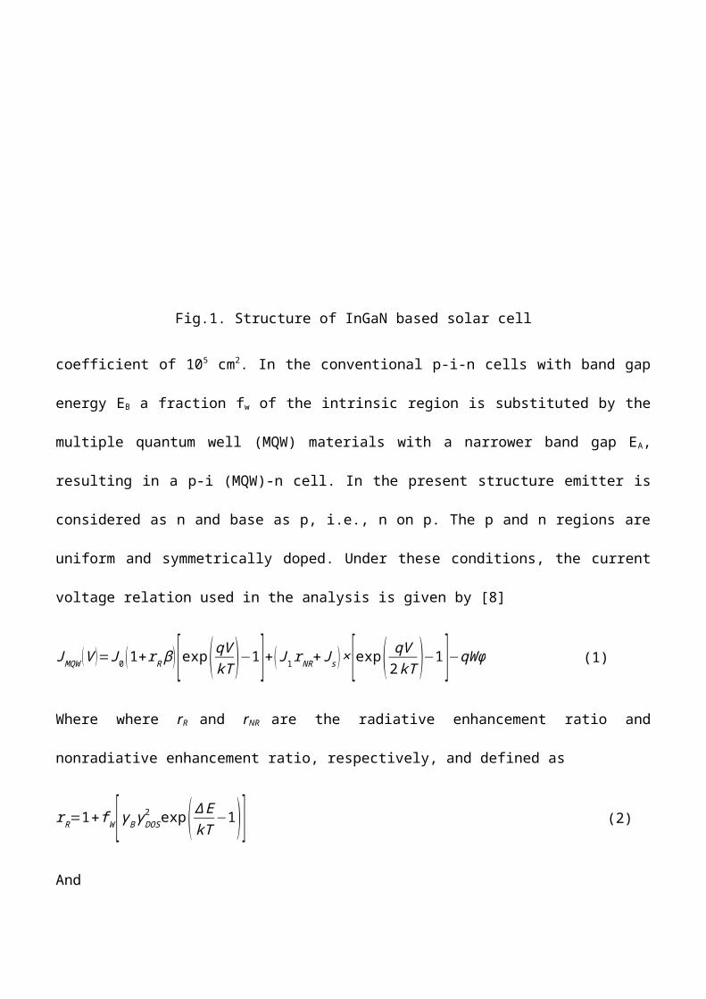
Fig.1. Structure of InGaN based solar cell
coefficient of 105 cm2. In the conventional p-i-n cells with band gap
energy EB a fraction fw of the intrinsic region is substituted by the
multiple quantum well (MQW) materials with a narrower band gap EA,
resulting in a p-i (MQW)-n cell. In the present structure emitter is
considered as n and base as p, i.e., n on p. The p and n regions are
uniform and symmetrically doped. Under these conditions, the current
voltage relation used in the analysis is given by [8]
JMQW (V )=J0 (1+rRβ)[exp(qVkT )−1]+(J1rNR+Js )× [exp( qV2kT )−1 ]−qWϕ (1)
Where where rR and rNR are the radiative enhancement ratio and
nonradiative enhancement ratio, respectively, and defined as
rR=1+fW[γBγDOS2 exp(∆EkT −1)] (2)
And
rNR=1+fW[γAγDOSexp( ∆E2kT−1)] (3)
The recombination current
Js=2NqniBνsγDOSexp( ∆EkT )(4)
N is the number of intrinsic region. The term is the flux of
incident photons absorbed by the multi quantum well solar cell, which
we have written as
ϕ=ϕB+NϕW (5)
Where ФB is the net flux of incident photons absorbed by the barrier
material Фw, the net flux of incident photons absorbed by the quantum
well and N, the number of well in the intrinsic region. The open
circuit voltage for the quantum well solar cell is given as
VOCQW=kTq ln(qrGϕB+J0 (1+rRβ )
J0 (1+rRβ ) )(6)
Defining the “generation enhancement ratio” as
rG=ϕA
ϕB
(7)
The efficiency of the solar cell is calculated as
η=JphVocFF
ϕo=JscVocFF
ϕo
(8)
Where, FF is the fill factor whose value is considered as FF = 0.85
and Ф0 is the incident irradiance per unit area in mW/cm2.
The quantum dot solar cell concept is proposed as a scheme for
increased solar cell efficiency. A theoretical model is presented for
simulation analysis of a InGaN based p – i – n quantum dot solar cell.
Authors [1] have analyzed the p-i-n quantum dot solar cell that is
given bellow. For the incident light of wavelength λ and ux F (λ) thefl
electron–hole generation rate at a depth z, is equal to
Gp (λ,z )=α (λ ) [1−R (λ ) ]F (λ )exp [−α (λ )z ]
(9)
Where R (λ) is the surface re ection coefficient and a (λ) is thefl
light absorption coefficient of GaN. For further calculations, we
Where R (λ) is the surface re ection coefficient and a (λ) is thefl
light absorption coefficient of GaN. For further further calculations,
we use the model of solar spectrum described by a black body curve,
corresponding to a temperature of 5760K. Hence, the spectral
distribution of the solar ux incident on the cell surface under thefl
condition 1 Sun, 1.5AM can be written as
F (λ )=3.53×10²¹¿ (10)
Where h is the Pluck’s constant, c is the velocity of light, k is The
Boltzmann’s constant, and T= 55760K. For the photo generated electron
current density at z=zp
jn (λ )=eF (λ ) [1−R (λ ) ] an (λ )
an (λ )2−1βn[bn+an (λ )−exp(zpan(λ)
Ln )[bn+an(λ) ]cosh(zp
Ln )+[1+bnan(λ)]sinh(zp
Ln )]¿(11)
Where e is the absolute value of the electronic charge
¿ (12)
The total photocurrent collected by p type is equal to
jnp=∫
0
λ1
jn (λ )dλ (13)
Therefore, the net photocurrent generated by light of given λ and
collected from i region is equal to
ji=e[∫0
λ1
jb (λ )dλ+∫λ1
λ2
jd (λ )dλ]
(14)
We can write the short-circuit current density of the cell as
jsc=fi(jnp+jpn+ji)
(15)
Where the transport factor fi (=0.12) represents the mean probability
of an electron or hole crossing the i region without capturing and
recombination. Using the standard super position model of solar cell,
the current density can be presented as
j=jsc−j0[exp(eVkT )−1 ]
(16)
Where J0 is the reverse saturation current of the junction. The
reverse saturation current is formed by the minority carriers that are
generated at the depletion layer edges Js1 and in the interior of the
i region Js2 due to thermal excitation. Such a current is controlled by
the band gap of GaN, EgB and average band gap of the i region.
Eeff=[1−vdnd ]EgB+vdndEgD (17)
Where, EgD is the band gap of QDs, which has to be taken as
Eg (InAs )+confinementenergy
Detailed balance between the incident and emitted radiation in thermal
equilibrium give the following expression for the Thermal generation
current in the i region
js2=Aeffexp (−EeffvkT
)
(18)
Here v is the ideality factor.
Aeff=e4πn2 kTc2h3
Eeff2
(19)
n is the average refractive index of the i region. The other dark
Current component js1 has the usual form
js1=Aexp(−EgB
vkT )
(20)
Here Nc and NV are the effective density of state in GaN, ND and NA are
the donor and acceptor concentration in the n-type and p-type regions,
correspondingly. The open circuit voltage for the quantum well solar
cell is given as
Voc=(k∗Tq )∗2.303∗log (jsc
jo+1) (21)
We can now calculate the cell power conversion efficiency at the
maximum power point. Finally, we have
ɳ=VoptJopt
P0=kTe
topt [jsc−j0 (etopt−1 ) ]P0
(22)
Where P0= 116 mW/cm2 is the incident solar ux (for 1 sun, AM1.5fl
condition) and topt has to be de ned from the equationfi
etopt (1+topt)−1=jscj0
(23)
The calculations show that the inclusion of the QDs in the intrinsic
region does indeed enhance short circuit current without signi cantfi
losses in the open circuit voltage and result signi cantly improvedfi
cell efficiency.
For design purpose, we considered the doping on the n and p sides to
be 1018cm-3, assumed an intrinsic region thickness to be 250 nm and the
fraction of the intrinsic region volume occupied by the quantum well
material in the MQW cells to be fw= 0.5 [8]. The energy gaps of the
InGaN alloys that should be used for the cells are optimized assuming
a perfect quantum retort of the materials. The surface and the rear
recombination velocities were taken to be 103 cm/s. The carrier
diffusion lengths and coefficients of the identified InGaN alloys are
assumed to be 125×10-6 cm and 25 cm2/s for electrons and 79×10-6 cm and
9 cm2 /s for holes. The lattice mismatch between the well and base
line gap is around 2%.
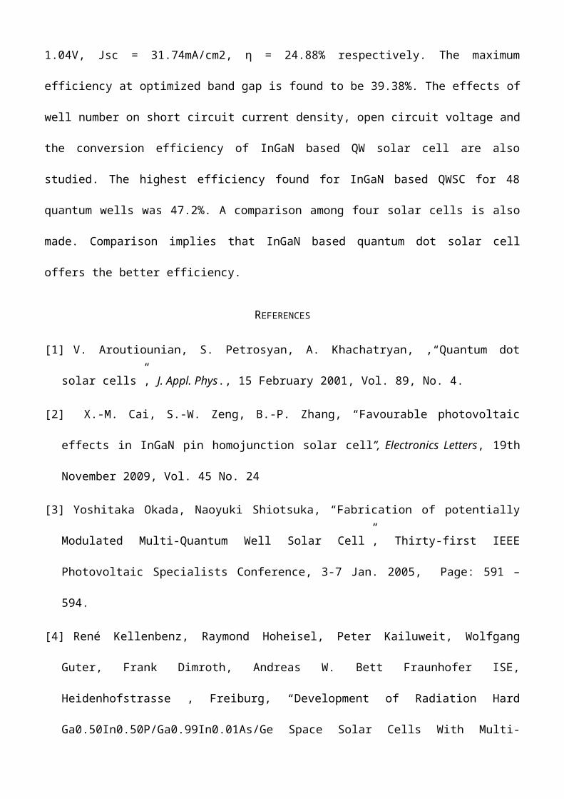
III.RESULT & DISCUSSION
The performance of the solar cell is deliberated in terms of short
circuit current density (Jsc), open circuit voltage (Voc) and
efficiency (η). In our experiment, we have analyzed open circuit
voltage, short circuit current and efficiency for p-n and p-i-n,
quantum well and quantum dot InGaN based solar cell by varying band
gap energy. Band gap optimization has been done to reach the maximum
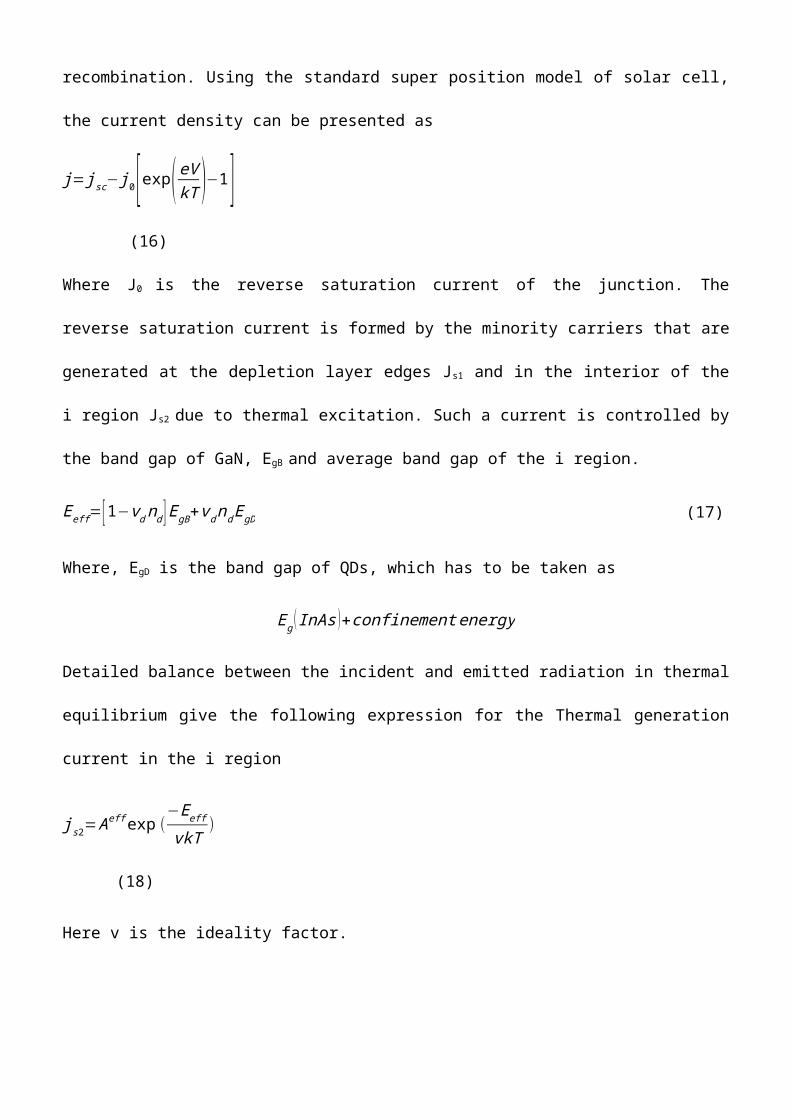
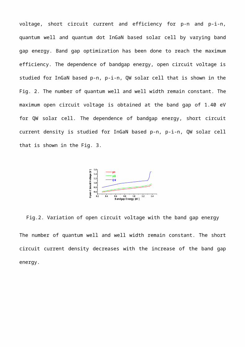
efficiency. The dependence of bandgap energy, open circuit voltage is
studied for InGaN based p-n, p-i-n, QW solar cell that is shown in the
Fig. 2. The number of quantum well and well width remain constant. The
maximum open circuit voltage is obtained at the band gap of 1.40 eV
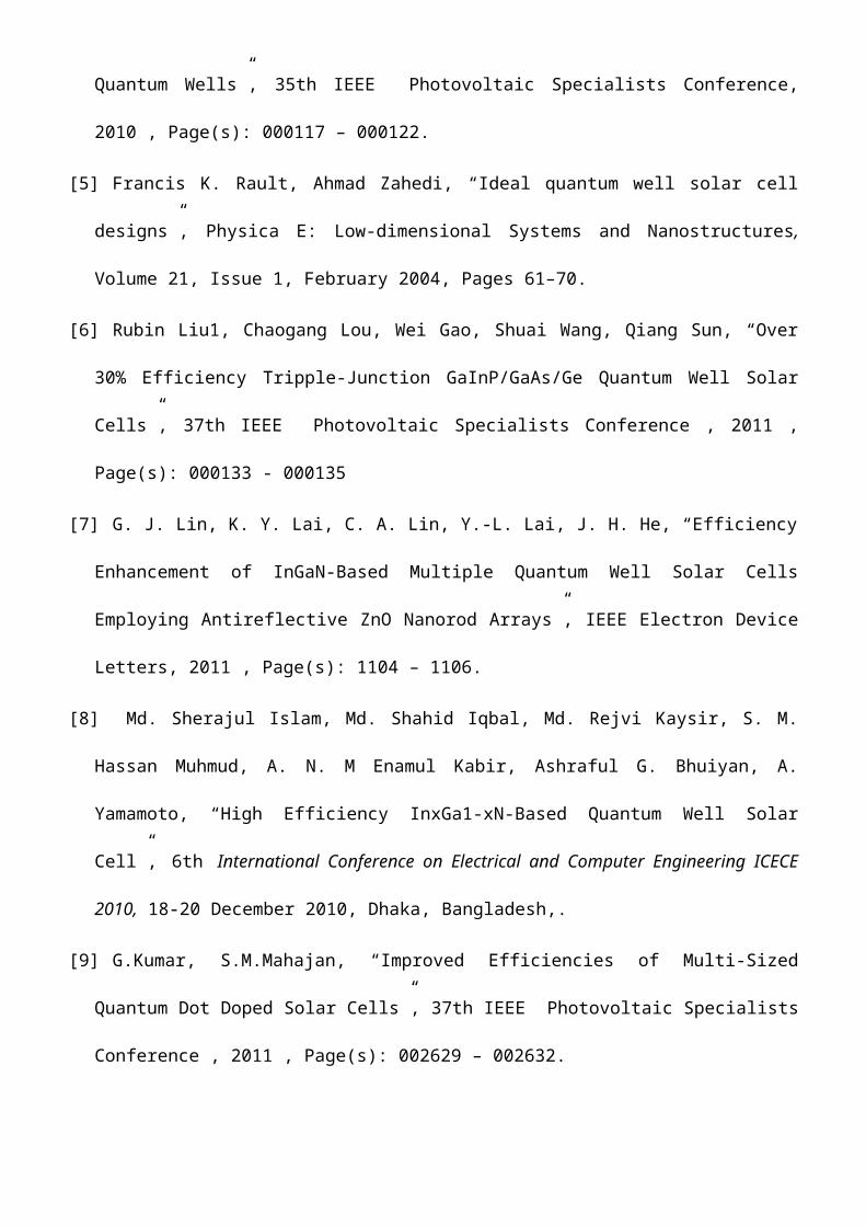
for QW solar cell. The dependence of bandgap energy, short circuit
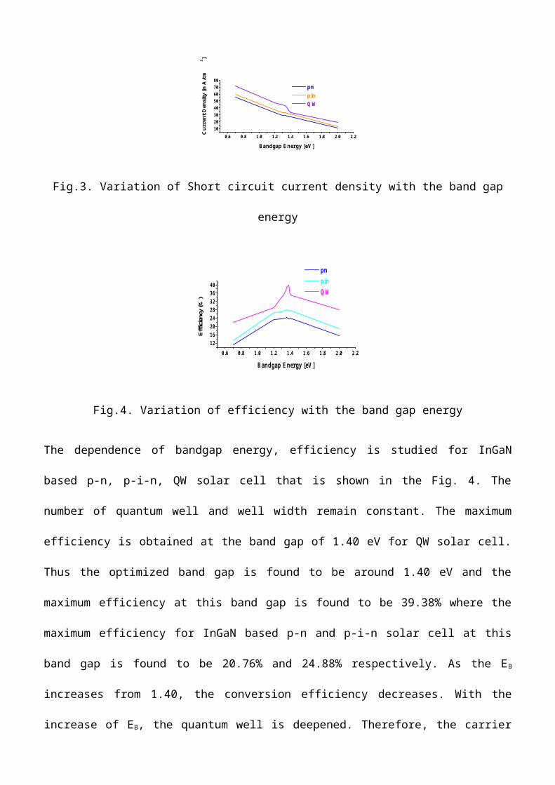
current density is studied for InGaN based p-n, p-i-n, QW solar cell
that is shown in the Fig. 3.
0.2 0.4 0.6 0.8 1.0 1.2 1.40.6
0.8
1.0
1.2
1.4
1.6
Open Circuit Voltage [V
]
B andgap E nergy [eV ]
pn pin Q W
Fig.2. Variation of open circuit voltage with the band gap energy
The number of quantum well and well width remain constant. The short
circuit current density decreases with the increase of the band gap
energy.
0.6 0.8 1.0 1.2 1.4 1.6 1.8 2.0 2.21020304050607080
Current Density [m
A/cm
2 ]
B andgap E nergy [eV ]
pn pin Q W
Fig.3. Variation of Short circuit current density with the band gap
energy
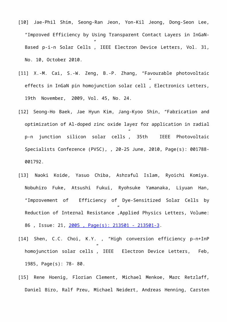
0.6 0.8 1.0 1.2 1.4 1.6 1.8 2.0 2.21216202428323640
Efficiency (%)
B andgap E nergy [eV ]
pn pin Q W
Fig.4. Variation of efficiency with the band gap energy
The dependence of bandgap energy, efficiency is studied for InGaN
based p-n, p-i-n, QW solar cell that is shown in the Fig. 4. The
number of quantum well and well width remain constant. The maximum
efficiency is obtained at the band gap of 1.40 eV for QW solar cell.
Thus the optimized band gap is found to be around 1.40 eV and the
maximum efficiency at this band gap is found to be 39.38% where the
maximum efficiency for InGaN based p-n and p-i-n solar cell at this
band gap is found to be 20.76% and 24.88% respectively. As the EB
increases from 1.40, the conversion efficiency decreases. With the
increase of EB, the quantum well is deepened. Therefore, the carrier
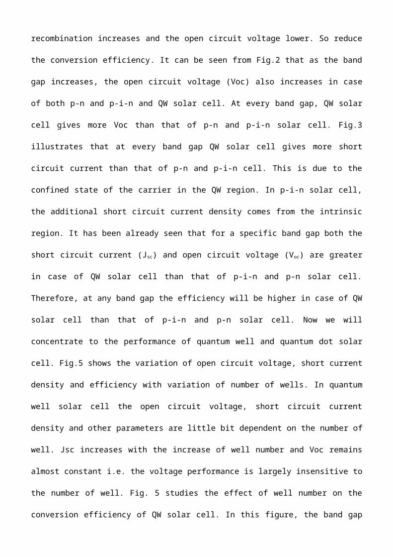
recombination increases and the open circuit voltage lower. So reduce
the conversion efficiency. It can be seen from Fig.2 that as the band
gap increases, the open circuit voltage (Voc) also increases in case
of both p-n and p-i-n and QW solar cell. At every band gap, QW solar
cell gives more Voc than that of p-n and p-i-n solar cell. Fig.3
illustrates that at every band gap QW solar cell gives more short
circuit current than that of p-n and p-i-n cell. This is due to the
confined state of the carrier in the QW region. In p-i-n solar cell,
the additional short circuit current density comes from the intrinsic
region. It has been already seen that for a specific band gap both the
short circuit current (Jsc) and open circuit voltage (Voc) are greater
in case of QW solar cell than that of p-i-n and p-n solar cell.
Therefore, at any band gap the efficiency will be higher in case of QW
solar cell than that of p-i-n and p-n solar cell. Now we will
concentrate to the performance of quantum well and quantum dot solar
cell. Fig.5 shows the variation of open circuit voltage, short current
density and efficiency with variation of number of wells. In quantum
well solar cell the open circuit voltage, short circuit current
density and other parameters are little bit dependent on the number of
well. Jsc increases with the increase of well number and Voc remains
almost constant i.e. the voltage performance is largely insensitive to
the number of well. Fig. 5 studies the effect of well number on the
conversion efficiency of QW solar cell. In this figure, the band gap
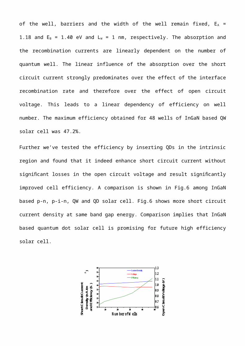
of the well, barriers and the width of the well remain fixed, EA =
1.18 and EB = 1.40 eV and LW = 1 nm, respectively. The absorption and
the recombination currents are linearly dependent on the number of
quantum well. The linear influence of the absorption over the short
circuit current strongly predominates over the effect of the interface
recombination rate and therefore over the effect of open circuit
voltage. This leads to a linear dependency of efficiency on well
number. The maximum efficiency obtained for 48 wells of InGaN based QW
solar cell was 47.2%.
Further we’ve tested the efficiency by inserting QDs in the intrinsic
region and found that it indeed enhance short circuit current without
signi cant losses in the open circuit voltage and result signi cantlyfi fi
improved cell efficiency. A comparison is shown in Fig.6 among InGaN
based p-n, p-i-n, QW and QD solar cell. Fig.6 shows more short circuit
current density at same band gap energy. Comparison implies that InGaN
based quantum dot solar cell is promising for future high efficiency
solar cell.
10 20 30 40 5015
20
25
30
35
40
45
50
55
60
10 20 30 40 500.60.70.80.91.01.11.21.3
10 20 30 40 5015
20
25
30
35
40
45
50
55
60
Open Circuit Voltage (V)
Short Circuit Current
Density (mA/cm
2)
and Efficiency (%)
N um ber of W ells
E fficiency
V oltage C urrent D ensity
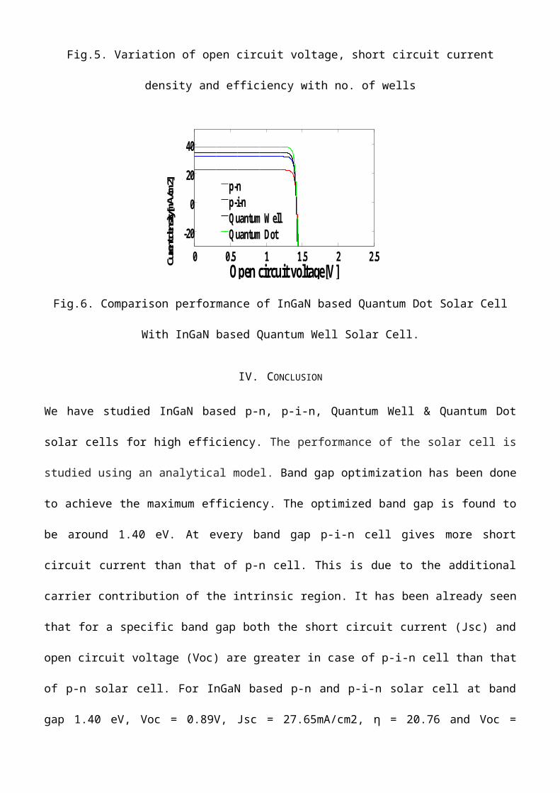
Fig.5. Variation of open circuit voltage, short circuit current
density and efficiency with no. of wells
0 0.5 1 1.5 2 2.5-20
0
20
40
O pen circuit voltage[V]Curent density[mA/cm2]
p-np-i-nQ uantum W ellQ uantum Dot
Fig.6. Comparison performance of InGaN based Quantum Dot Solar Cell
With InGaN based Quantum Well Solar Cell.
IV. CONCLUSION
We have studied InGaN based p-n, p-i-n, Quantum Well & Quantum Dot
solar cells for high efficiency. The performance of the solar cell is
studied using an analytical model. Band gap optimization has been done
to achieve the maximum efficiency. The optimized band gap is found to
be around 1.40 eV. At every band gap p-i-n cell gives more short
circuit current than that of p-n cell. This is due to the additional
carrier contribution of the intrinsic region. It has been already seen
that for a specific band gap both the short circuit current (Jsc) and
open circuit voltage (Voc) are greater in case of p-i-n cell than that
of p-n solar cell. For InGaN based p-n and p-i-n solar cell at band
gap 1.40 eV, Voc = 0.89V, Jsc = 27.65mA/cm2, η = 20.76 and Voc =
1.04V, Jsc = 31.74mA/cm2, η = 24.88% respectively. The maximum
efficiency at optimized band gap is found to be 39.38%. The effects of
well number on short circuit current density, open circuit voltage and
the conversion efficiency of InGaN based QW solar cell are also
studied. The highest efficiency found for InGaN based QWSC for 48
quantum wells was 47.2%. A comparison among four solar cells is also
made. Comparison implies that InGaN based quantum dot solar cell
offers the better efficiency.
REFERENCES
[1] V. Aroutiounian, S. Petrosyan, A. Khachatryan, ,“Quantum dot
solar cells”, J. Appl. Phys., 15 February 2001, Vol. 89, No. 4.
[2] X.-M. Cai, S.-W. Zeng, B.-P. Zhang, “Favourable photovoltaic
effects in InGaN pin homojunction solar cell”, Electronics Letters, 19th
November 2009, Vol. 45 No. 24
[3] Yoshitaka Okada, Naoyuki Shiotsuka, “Fabrication of potentially
Modulated Multi-Quantum Well Solar Cell”, Thirty-first IEEE
Photovoltaic Specialists Conference, 3-7 Jan. 2005, Page: 591 –
594.
[4] René Kellenbenz, Raymond Hoheisel, Peter Kailuweit, Wolfgang
Guter, Frank Dimroth, Andreas W. Bett Fraunhofer ISE,
Heidenhofstrasse , Freiburg, “Development of Radiation Hard
Ga0.50In0.50P/Ga0.99In0.01As/Ge Space Solar Cells With Multi-
Quantum Wells”, 35th IEEE Photovoltaic Specialists Conference,
2010 , Page(s): 000117 – 000122.
[5] Francis K. Rault, Ahmad Zahedi, “Ideal quantum well solar cell
designs”, Physica E: Low-dimensional Systems and Nanostructures,
Volume 21, Issue 1, February 2004, Pages 61–70.
[6] Rubin Liu1, Chaogang Lou, Wei Gao, Shuai Wang, Qiang Sun, “Over
30% Efficiency Tripple-Junction GaInP/GaAs/Ge Quantum Well Solar
Cells”, 37th IEEE Photovoltaic Specialists Conference , 2011 ,
Page(s): 000133 - 000135
[7] G. J. Lin, K. Y. Lai, C. A. Lin, Y.-L. Lai, J. H. He, “Efficiency
Enhancement of InGaN-Based Multiple Quantum Well Solar Cells
Employing Antireflective ZnO Nanorod Arrays”, IEEE Electron Device
Letters, 2011 , Page(s): 1104 – 1106.
[8] Md. Sherajul Islam, Md. Shahid Iqbal, Md. Rejvi Kaysir, S. M.
Hassan Muhmud, A. N. M Enamul Kabir, Ashraful G. Bhuiyan, A.
Yamamoto, “High Efficiency InxGa1-xN-Based Quantum Well Solar
Cell”, 6th International Conference on Electrical and Computer Engineering ICECE
2010, 18-20 December 2010, Dhaka, Bangladesh,.
[9] G.Kumar, S.M.Mahajan, “Improved Efficiencies of Multi-Sized
Quantum Dot Doped Solar Cells”, 37th IEEE Photovoltaic Specialists
Conference , 2011 , Page(s): 002629 – 002632.
[10] Jae-Phil Shim, Seong-Ran Jeon, Yon-Kil Jeong, Dong-Seon Lee,
“Improved Efficiency by Using Transparent Contact Layers in InGaN-
Based p-i-n Solar Cells”, IEEE Electron Device Letters, Vol. 31,
No. 10, October 2010.
[11] X.-M. Cai, S.-W. Zeng, B.-P. Zhang, “Favourable photovoltaic
effects in InGaN pin homojunction solar cell”, Electronics Letters,
19th November, 2009, Vol. 45, No. 24.
[12] Seong-Ho Baek, Jae Hyun Kim, Jang-Kyoo Shin, “Fabrication and
optimization of Al-doped zinc oxide layer for application in radial
p-n junction silicon solar cells”, 35th IEEE Photovoltaic
Specialists Conference (PVSC), , 20-25 June, 2010, Page(s): 001788-
001792.
[13] Naoki Koide, Yasuo Chiba, Ashraful Islam, Ryoichi Komiya.
Nobuhiro Fuke, Atsushi Fukui, Ryohsuke Yamanaka, Liyuan Han,
“Improvement of Efficiency of Dye-Sensitized Solar Cells by
Reduction of Internal Resistance”,Applied Physics Letters, Volume:
86 , Issue: 21, 2005 , Page(s): 213501 - 213501-3.
[14] Shen, C.C. Choi, K.Y. , “High conversion efficiency p-n+InP
homojunction solar cells”, IEEE Electron Device Letters, Feb,
1985, Page(s): 78- 80.
[15] Rene Hoenig, Florian Clement, Michael Menkoe, Marc Retzlaff,
Daniel Biro, Ralf Preu, Michael Neidert, Andreas Henning, Carsten
Mohr, Weiming Zhang, “Paste Development for Screen Printed MC-SI
MWT Solar Cell Exceeding 17% Efficiency”, 35th IEEE Photovoltaic
Specialists Conference, 2010 , Page(s): 003167 - 003172.
[16] Ki Hwan Kim, Min Sik Kim, Byung Tae Ahn, Jae Ho Yun, Kyung
HoonYoon, “Improvement of CIGS microstructure and its effect on the
conversion efficiency of CIGS solar cells”, IEEE 4th World
Conference on Photovoltaic Energy Conversion , 2006 , Page(s): 575
- 578.
[17] Arai, Y. Ishii, M. ; Shinohara, H. ; Yamazaki, S. , “A single
p-i-n junction amorphous-silicon solar cell with conversion
efficiency of 12.65%”, Electron Device Letters, IEEE, Aug. 1991,
Volume: 12, Issue: 8 ,Page(s): 460 – 461.
[18] Bailat, J., Domine, D. ; Schluchter, R. ; Steinhauser,
J. ; Fay, S. ; Freitas, F. ; Bucher, C. ; Feitknecht,
L. ; Niquille, X. ; Tscharner, T. ; Shah, A. ; Ballif, C., “
High-Efficiency P-I-N Microcrystalline and Micromorph Thin Film
Silicon Solar Cells Deposited on LPCVD Zno Coated Glass
Substrates”, IEEE 4th World Conference on Photovoltaic Energy
Conversion, May 2006, Volume: 2 Page(s): 1533 – 1536.
[19] Feng, Shih-Wei , Lai, Chih-Ming ; Chen, Chien-Hsun ; Sun, Wen-
Ching ; Tu, Li-Wei , “Theoretical simulations of the effects of
the indium content, thickness, and defect density of the i-layer on
the performance ofp-i-n InGaN single homojunction solar cells”,
Journal of Applied Physics, Nov 2010, Volume: 108 , Issue:
9 ,Page(s): 093118 - 093118-7.
[20] A.Luqueand A.Martí,“ On the Partial Filling of the Intermediate
Band In IB Solar Cells,” IEEE transaction on electron devices,
Vol.57, No.6, June, 2010.
[21] A.Luqueand01 A.Martí,“On the Partial Filling of the Intermediate
Band In IB Solar Cells,” IEEE transaction on electron devices,
Vol.57, No.6, June, 2010.


