Embed Size (px)
Citation preview

This content has been downloaded from IOPscience. Please scroll down to see the full text.
Download details:
IP Address: 134.157.146.58
This content was downloaded on 01/04/2015 at 20:24
Please note that terms and conditions apply.
Excitation transfer in stacked quantum dot chains
View the table of contents for this issue, or go to the journal homepage for more
2015 Semicond. Sci. Technol. 30 055005
(http://iopscience.iop.org/0268-1242/30/5/055005)
Home Search Collections Journals About Contact us My IOPscience
Excitation transfer in stacked quantum dotchains
Songphol Kanjanachuchai1, Ming Xu2, Alexandre Jaffré2,Apichart Jittrong1, Thitipong Chokamnuai1, Somsak Panyakeow1 andMohamed Boutchich2
1 Semiconductor Device Research Laboratory, Department of Electrical Engineering, Faculty ofEngineering, Chulalongkorn University, Bangkok 10330, Thailand2GeePs, CNRS UMR8507, CentraleSupelec, Univ Paris-Sud, Sorbonne Universités—UPMC, Univ Paris06, 11 rue Joliot-Curie, Plateau de Moulon, 91192 Gif-sur-Yvette Cedex, France
E-mail: [email protected]
Received 10 December 2014, revised 3 February 2015Accepted for publication 27 February 2015Published 31 March 2015
AbstractStacked InAs quantum dot chains (QDCs) on InGaAs/GaAs cross-hatch pattern (CHP) templatesyield a rich emission spectrum with an unusual carrier transfer characteristic compared toconventional quantum dot (QD) stacks. The photoluminescent spectra of the controlled, singleQDC layer comprise multiple peaks from the orthogonal QDCs, the free-standing QDs, the CHP,the wetting layers and the GaAs substrate. When the QDC layers are stacked, employing a 10 nmGaAs spacer between adjacent QDC layers, the PL spectra are dominated by the top-most stack,indicating that the QDC layers are nominally uncoupled. Under high excitation power densitieswhen the high-energy peaks of the top stack are saturated, however, low-energy PL peaks fromthe bottom stacks emerge as a result of carrier transfers across the GaAs spacers. These uniquePL signatures contrast with the state-filling effects in conventional, coupled QD stacks and serveas a means to quickly assess the presence of electronic coupling in stacks of dissimilar-sizednanostructures.
S Online supplementary data available from stacks.iop.org/SST/30/055005/mmedia
Keywords: quantum dot chains, photoluminescent mapping, electronic coupling, cross-hatchpatterns, InAs, vertical stacking, excitation transfer
(Some figures may appear in colour only in the online journal)
1. Introduction
Semiconductor quantum dots (QDs) grown by molecularbeam epitaxy (MBE) are often stacked in order to increase theactive optical volume and to tune the emission or detectionwavelength and polarization of the QD ensembles [1, 2].Stacking QDs is achieved through thin spacer layers whichphysically separate but often electronically couple adjacentQD layers [3]. Understanding the coupling nature of verticallystacked QD structures is of fundamental importance to theoperation and optimization of QD-based devices such asmemory [4], lasers [5] and solar cells [6, 7]. Though useful,coupling is not always necessary or desired, particularly forbroadband applications which benefit from the superposition
of different wavelengths from individual QD layers [8]. Ifpresent, electronic coupling results in the lowering of theexcitonic ground-state (GS) energy, and consequently a red-shift of photoluminescent peak [3, 9]. The degree of couplingis thus usually inferred from the magnitude of the energeticred-shift relative to those emitted from a single QD layerstructure [3]. This approach can be misleading in stacked QDsas the strain profile at the growth front is affected by theunderlying nanostructures: subsequent QD layers usuallynucleate at a lower deposition amount [9, 10]. If grown at thesame two-dimensional (2D) equivalent thickness throughout,upper QD layers would be bigger than those of the lower QDlayers, with a concomitant red-shift due to size—not cou-pling. One way to unambiguously identify the presence and
Semiconductor Science and Technology
Semicond. Sci. Technol. 30 (2015) 055005 (7pp) doi:10.1088/0268-1242/30/5/055005
0268-1242/15/055005+07$33.00 © 2015 IOP Publishing Ltd Printed in the UK1
evaluate the strength of coupling is to vary the spacer thick-ness and observe the changes in PL signals as a result ofexcitation transfer of carriers. This approach has been adoptedto study coupling between, for example, stacked QDs [11]and stacked quantum dots and wells [12]. Alternatively, onecan fix the spacer thickness, vary the size of each stack,perform PL measurements and simply count the number ofGS peaks: a single (multiple) GS peak indicates the presence(absence) of coupling [11]. This article adopts the latterapproach to study an unusual coupling property of stackedquantum dot chains (QDCs) on cross-hatch pattern (CHP)templates.
QDCs or laterally-coupled QDs have garnered significantinterest in the past decade [13] and have recently gainedrenewed interest due to their unique geometry suitable forfundamental transport studies [14] and polarization-sensitiveoptoelectronic devices [15]. However, QDCs are rarely stu-died in stacked forms due to their complex optical char-acteristics [16], particularly when coupling cansimultaneously occur laterally and vertically as is the casehere. In this paper, stacked InAs QDCs on InGaAs/GaAsCHP templates grown by molecular beam epitaxy (MBE) arecharacterized by photoluminescence (PL) and a complete PLfingerprint of QDCs/CHP structures is reported. Under highexcitation power densities, stacked QDCs do not exhibit state-filling effects as would be observed in stacked QDs. Theotherwise excited-state carriers are instead transferred towardthe lower QDC layer, an effect attributed to the combinationof extended wavefunctions, resonant tunnelling andthermalization.
2. Experimental
The structures investigated comprise multiple stacks of InAsQDCs grown on partially-relaxed InGaAs film on GaAs bysolid-source MBE Using Riber’s 32P MBE system, and afterin situ thermal cleaning of GaAs (001) surface, growth startsfrom 300 nm GaAs buffer layer, followed by 25 nmIn0.2Ga0.8As, 10 nm GaAs spacer, and 1, 3, or 5 stacks ofInAs QDC/10 nm GaAs spacer pairs. The cross-hatch patternsurface of the InGaAs layer serves as a template on whichchains of QDs form along the orthogonal [110] and [11̄0]directions. The smoothness of the growth fronts and the for-mation of QDs are monitored in situ via streaky and spottyreflection high-energy electron diffraction (RHEED) patterns,respectively. Each QD layer is grown until the RHEED pat-tern changes from streaks to spots, i.e., at the onset of QDformation. The 2D equivalent thicknesses of the bottom-moststack are 1.7 monolayer (ML) and the remaining stacks are1.3ML. Finally, all samples are capped with 100 nm GaAsfor PL measurements. Two PL set-ups are employed. Forfree-space, macro-PL setup, the samples are fixed in a cryo-stat, excited by a broad beam (2.39 mm spot size), 514.5 nmAr+ laser, and emission detected by a liquid nitrogen-cooledInGaAs point detector (Hamamatsu’s G7754) using standardlock-in techniques. For confocal, micro-PL setup, the sampleis mounted on a piezoelectric-driven platform (Witec’s
alpha300), excited by a narrow beam (∼1 μm spot size) fre-quency-doubled 532 nm Nd:YAG laser operating in con-tinuous mode, and emission detected by a thermoelectrically-cooled InGaAs array detector (Andor’s DU491A). Spatial-and energy-resolved PL maps are acquired from the micro-PLsetup by raster scanning and simultaneously collecting pointspectra. All maps shown represent PL intensities integratedover a 10 meV bandwidth around energies of interest.
3. Results and discussion
Conventional InAs Stranski–Krastanow (SK) QDs grown onflat GaAs (001) are randomly distributed and typically emit asingle PL peak at around 1 μm with a full width at halfmaximum (FWHM) of a few 10 s meV [17]. Certain growthconditions can extend the wavelength to the 1.3–1.55 μmtelecom window [18] or lead to bimodal or multimodal sizedistributions with multiple PL peaks [19–21], while randomdistribution remains. In contrast, InAs QDs grown on CHPsare guided, forming chains along the orthogonal [110] and[11̄0] directions, each direction with its own size, size dis-tribution, and wetting layer (WL) due to the asymmetry of theunderlying dislocations [22]. The formation of QDs along theorthogonal dislocation chains has been established by plan-view transmission electron microscopy (TEM) [23], whereasvertical correlation of QDs with 10 nm GaAs spacer has beenconfirmed by cross-sectional TEM [24]. The 60° dislocationsat the lower InGaAs/GaAs interface, typical in zincblendeheteroepitaxy, cause surface strain fields that affect adatomsmotion during growth [25], but do not affect the intrinsicemission efficiency of the overlying QDs [26]. The PLspectrum of a QDC layer would thus contain many more PLpeaks than those of conventional SK QDs due to the co-existence of many optically active structures.
This section is divided into three parts. The first partdescribes the PL maps and spectra of the 1-stack QDC layer,showing all the possible luminescent peaks. The second partshows that luminescence is dominated by the uppermost QDClayer which is nominally uncoupled to the underlying QDClayers. The third part shows that the luminescence from thebottom QDC layers emerges at high excitation level, andprovides a qualitative explanation of the underlyingmechanism.
3.1. Single QDC layer: basic emission peaks
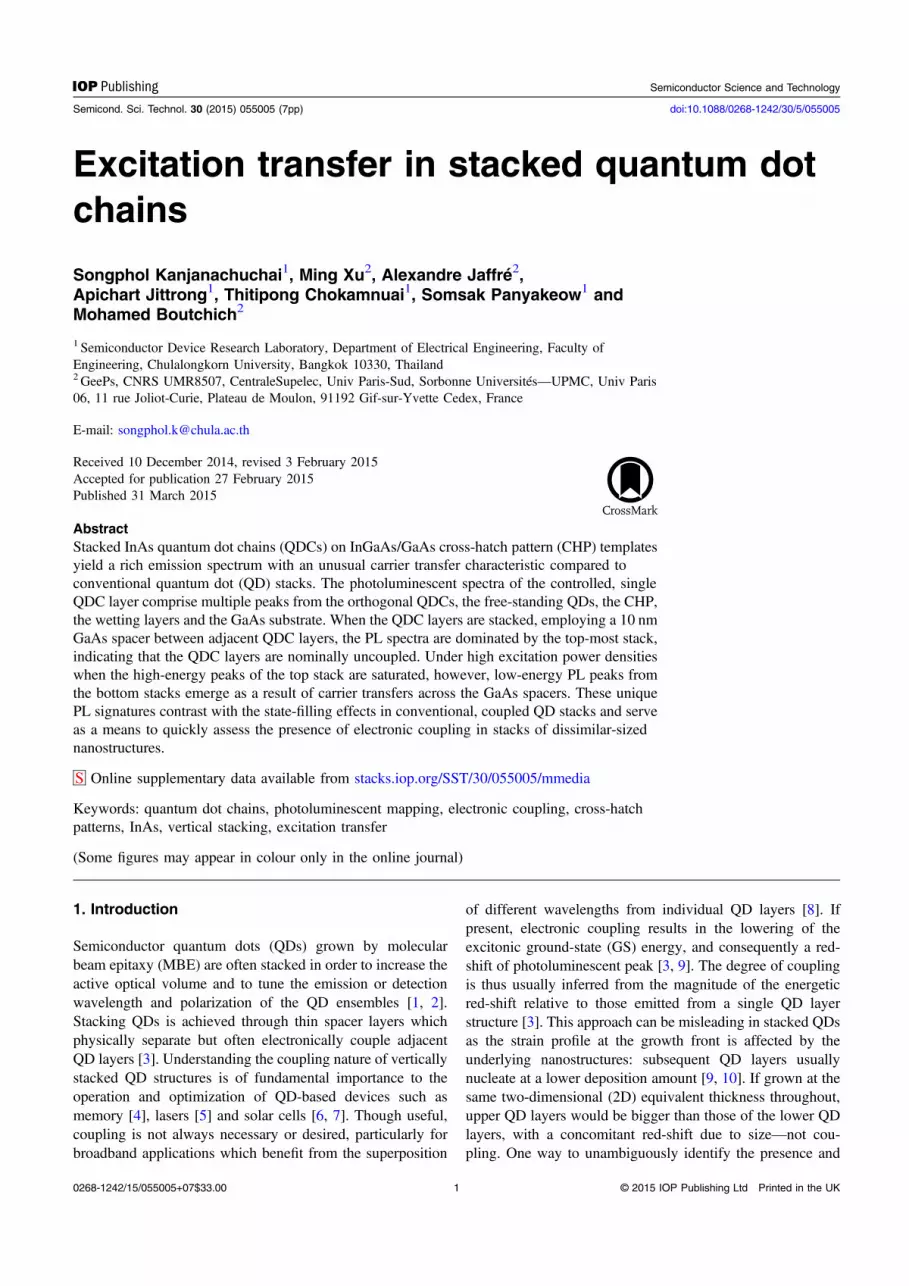
The 1-stack QDC sample emits in the 1–1.4 eV range similarto conventional SK QDs, but with a much richer opticalfeature. Figures 1(a)–(f) show spatial- and energy-resolvedspectral maps of the same 20 × 20 μm2 area of the sample at80 K. The PL maps, integrated over increasing energies from1.005 eV in figure 1(a) to 1.275 eV in figure 1(f), show spa-tially non-uniform emissions with a cross-hatch patternresembling the surface undulation of the underlying InGaAs/GaAs template. Figure 1(a) shows that at 1 eV, the lowerenergetic end of the spectra, emissions emerge from brightpatches which look like stripes along the [11̄0] direction. The
2
Semicond. Sci. Technol. 30 (2015) 055005 S Kanjanachuchai et al

stripes become clearer and better resolved as the energyincreases to 1.045 eV in figure 1(b). The dottiness of the linesmaking up the stripes is simply a reflection of the variation inlocal QD density, in good agreement with the morphology ofuncapped samples (see the supplementary data, available atstacks.iop.org/SST/30/055005/mmedia). When the energyincreases to 1.105 eV in figure 1(c), emissions from theexisting [11̄0] direction begin to fade while those from theorthogonal, [110] direction emerge. The emissions from the[110] and [11̄0] stripes overlap and yield the characteristicCHP luminescence observed in figure 1(c). As the energycontinues to increase to 1.195 eV in figure 1(d), the [11̄0]emission peters out, whereas the [110] emission intensifies.And as the energy keeps on increasing to 1.245 eV infigure 1(e) and 1.275 eV in figure 1(f), the [110] and [11̄0]emissions are extinguished, replaced by bright patchesemerging in the previously dark areas—i.e., the bright/dark
regions in figures 1(a) and (f) are reversed. (The reversal iseasily recognized in the first video in the supplementary data).
The QDs can be categorized, in evolution sequence [27]and with corresponding labels shown in figure 1(d), into fourdistinct groups: 1. at the intersection of the orthogonal [110]and [11̄0] dislocations, 2. on the [11̄0] dislocation lines, 3. onthe [110] dislocation lines, and 4. on the remaining areas. Thefour QD ensembles emit slightly differently. Figure 1(g)shows point spectra at pixels 1–4 in figure 1(d), corre-sponding to the four QD ensembles above. Emissions frompixels 1–3 comprise two principal peaks: a broad peak cen-tered at around 1.15 eV and a narrow peak at 1.27 eV. Incontrast, emission from pixel 4 comprises only one narrowpeak, also centered at 1.27 eV.
The broad peaks result from QD chains along the [11̄0]and [110] directions as unequivocally proven by microscopyand spectroscopy. The micro-PL maps in figures 1(a)–(f)
Figure 1. PL of a single InAs QD chain layer on an InGaAs/GaAs cross-hatch pattern. Same-area, 20 × 20 μm2 micro-PL maps at increasingintegrated intensity from (a) 1.005 to (b) 1.045, (c) 1.105, (d) 1.195, (e) 1.245 and (f) 1.275 eV. Spectra at pixels 1–4 in (d) are shown in (g):pixel 1 is taken at an intersection between [11̄0] and [110] dislocation lines, 2 on a [11̄0] dislocation line, 3 on a [110] dislocation line, and 4on a dislocations-free area. (h) Macro-PL spectra measured at increasing excitation power density from, bottom to top, I= 0.11 W cm−2 to 2,4, 10, 20, 30, 40 and 50 times I. The scale bars in (a)–(f) are 4 μm. Spectra in (g) are offset for clarity.
3
Semicond. Sci. Technol. 30 (2015) 055005 S Kanjanachuchai et al
provide the microscopic proof, whereas the macro-PL spectrain figure 1(h) provide the spectroscopic confirmation. It haslong been known that the underlying InGaAs/GaAs CHPs areasymmetric: the [11̄0] stripes nucleate earlier, have greaterdensity, and result in surface steps which are taller than the[110] stripes [28]. The asymmetry is transferred to the over-grown layers, resulting in QDs along the [11̄0] directionforming slightly earlier and are thus taller and emit at a lowerenergy than those along the orthogonal [110] direction[22, 27, 29]. The microscopic images in figures 1(c)–(d)provide a clear visual evidence of QD luminescence dec-orating the [11̄0] and [110] stripes, at slightly different ener-gies. This small energy difference however cannot beresolved in the corresponding point spectra: figure 1(g) showsthat pixel 2, taken along the [11̄0] direction, emits at a slightlylower peak energy than pixel 3, taken along the orthogonal[110] direction. Though these two peaks are spatially resolvedin microscopy, they are spectrally unresolved as a result ofmicro-PL setup’s fast integration time. The macro-PL setup,in contrast, has a much longer integration time and can pro-vide complementary spectra with greater signal-to-noiseratios. Figure 1(h) shows excitation power-dependent macro-PL spectra of the same sample (but on a different area) at20 K. The lowest two energetic peaks—1.04 eV for the[11̄0]aligned QDs and 1.10 eV for the [110]-aligned QDs hi-lighted by the black arrows—can now be clearly resolved athigh excitation powers.
The narrow 1.27 eV peak is asymmetric: the left and rightsides of the 1.27 eV peak in figure 1(g) tail off slightly dif-ferently—a characteristic of two unresolved Gaussian peakswith different FWHM. The closely-spaced emissions arisefrom the superposition or spectral overlap of the small free-standing QDs and the underlying InGaAs CHP template. ThePL map in figure 1(f) shows that the areas that give off thisluminescence are those between the cross hatches whichhappen to be the nucleation sites for free-standing QDs, too.
The four small peaks between 1.3 and 1.47 eV (observedonly in the macro-PL setup as indicated by the grey arrows infigure 1(h)) are most likely associated with multiple wettinglayers, some of which were previously identified [22]. Forconventional InAs/GaAs SK QDs, a single WL exists andemits at around 1.44 eV. This is true even if bimodal sizedistributions are present [21], as long as the growth front isflat. For InAs QDs on InGaAs CHPs, the growth front is notflat. In fact, the surface steps in the [11̄0] and [110] directionsare different [28]. The WL underneath the QD chains alongthe [11̄0] and [110] directions can thus be expected to bedifferent—for example, they could form one-dimensionalwetting wires [30]—but similar structures investigated so farreported just a single WL energy [22].
The multiple WL peaks above are only observed close tothe carbon-impurity, 1.49 eV peak and the bulk GaAs,1.52 eV peak. Measurements taken at different areas wherethe 1.49 and 1.52 eV peaks are absent do not reveal themultiple WL peaks. This indicates the possibility that bulk Ccenters render ineffectual the carrier capture by QDs from theGaAs matrix and the WLs, and explain the elusiveness of themultiple WL luminescence. It is a normal practice for those
carrying out PL measurements to shine the exciting laser on aspot that yields the best signal and in so doing move awayfrom areas with large local concentrations of C, and hencemiss the WL peaks.
It is worth pointing out that the multimodal size dis-tribution of the 1-stack layer which gives rise to multipleemission peaks has not been optimized for broadband appli-cations. If desired, one can increase the inhomogeneity of thespectrum by, for instance, growing the QDs at a higher rate orsubjecting them to rapid thermal annealing [31]. In addition,one can also increase the luminous efficacy of real devices bysoft-annealing under hydrogen so that most defects are neu-tralized and do not adversely affect long-term reliability [22].
3.2. Multi-stack QDCs: dominant emission from top-mostlayers
In reflection-based PL set-ups, the 1-stack QDC layer enjoysan unobstructed output window but the 3- and 5-stack QDClayers may not. This depends on electronic coupling. If thestacked layers are coupled, they behave as a single ensembleand should enjoy an unobstructed output window as is thecase for the 1-stack sample. But if the stacked layers areuncoupled, luminescence from all the layers should bedetectable, unless some are obstructed—reabsorbed, scat-tered, or reflected—in which case the emissions are domi-nated by the overlying structures due to geometricaladvantage. Such behaviour in stacks of randomly distributedQDs cannot be proven through spectroscopy alone. But if therandom distribution is reduced, as is the case for QDCs, andwith PL mapping capability, it is possible to draw such aconclusion as shown below.
Figures 2(a)–(d) show the PL maps of the 3-stack QDCsample at increasing integrated energy from 1.075 eV infigure 2(a) to 1.235 eV in figure 2(d). Similarly, figures 2(e)–(h) show the PL maps of the 5-stack QDC sample from1.075 eV in figure 2(e) to 1.235 eV in figure 2(h) (see ani-mated videos in the supplementary data for the completeranges). The maps show luminescence which is CHP-like forthe 3-stack sample, but stripes-like for the 5-stack sample.Since adjacent stacks are separated by a 10 nm GaAs spacerwhich is sufficiently thin to allow coupling in conventionalSK QD stacks [11], a question emerges as to why CHP-likeluminescence similar to the 1-stack sample described above isnot observed in the 5-stack case, or is not more clearlyobserved in the 3-stack case because the bottom-most QDClayer for the three samples is identically grown, has the big-gest dot size and the lowest GS energies, and should thusprovide the same optical features (CHP-like) as observed inthe previous section. The maps shown in figure 2 insteadmore closely match the AFM morphologies of the top-mostQDC layer where the number density of QDs along the [110]direction is significantly reduced (see the supplementarydata), implying that the emission is dominated by the top-most layer. The bottom-most QDC layer buried along the[110] direction is almost undetectable; it can be barely dis-tinguished by the collinearity of bright or dark spots, asindicated by broken lines in figure 2.
4
Semicond. Sci. Technol. 30 (2015) 055005 S Kanjanachuchai et al
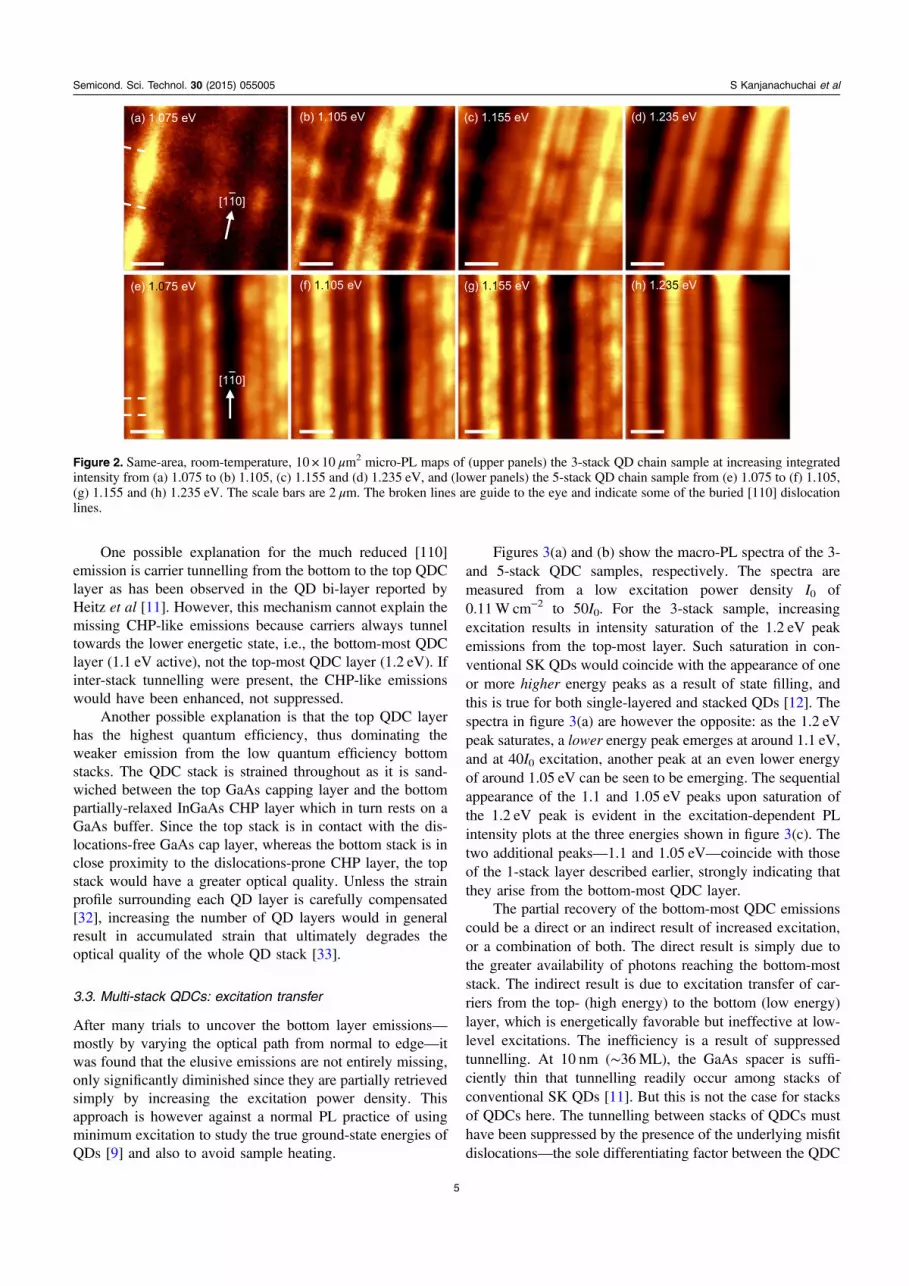
One possible explanation for the much reduced [110]emission is carrier tunnelling from the bottom to the top QDClayer as has been observed in the QD bi-layer reported byHeitz et al [11]. However, this mechanism cannot explain themissing CHP-like emissions because carriers always tunneltowards the lower energetic state, i.e., the bottom-most QDClayer (1.1 eV active), not the top-most QDC layer (1.2 eV). Ifinter-stack tunnelling were present, the CHP-like emissionswould have been enhanced, not suppressed.
Another possible explanation is that the top QDC layerhas the highest quantum efficiency, thus dominating theweaker emission from the low quantum efficiency bottomstacks. The QDC stack is strained throughout as it is sand-wiched between the top GaAs capping layer and the bottompartially-relaxed InGaAs CHP layer which in turn rests on aGaAs buffer. Since the top stack is in contact with the dis-locations-free GaAs cap layer, whereas the bottom stack is inclose proximity to the dislocations-prone CHP layer, the topstack would have a greater optical quality. Unless the strainprofile surrounding each QD layer is carefully compensated[32], increasing the number of QD layers would in generalresult in accumulated strain that ultimately degrades theoptical quality of the whole QD stack [33].
3.3. Multi-stack QDCs: excitation transfer
After many trials to uncover the bottom layer emissions—mostly by varying the optical path from normal to edge—itwas found that the elusive emissions are not entirely missing,only significantly diminished since they are partially retrievedsimply by increasing the excitation power density. Thisapproach is however against a normal PL practice of usingminimum excitation to study the true ground-state energies ofQDs [9] and also to avoid sample heating.
Figures 3(a) and (b) show the macro-PL spectra of the 3-and 5-stack QDC samples, respectively. The spectra aremeasured from a low excitation power density I0 of0.11W cm−2 to 50I0. For the 3-stack sample, increasingexcitation results in intensity saturation of the 1.2 eV peakemissions from the top-most layer. Such saturation in con-ventional SK QDs would coincide with the appearance of oneor more higher energy peaks as a result of state filling, andthis is true for both single-layered and stacked QDs [12]. Thespectra in figure 3(a) are however the opposite: as the 1.2 eVpeak saturates, a lower energy peak emerges at around 1.1 eV,and at 40I0 excitation, another peak at an even lower energyof around 1.05 eV can be seen to be emerging. The sequentialappearance of the 1.1 and 1.05 eV peaks upon saturation ofthe 1.2 eV peak is evident in the excitation-dependent PLintensity plots at the three energies shown in figure 3(c). Thetwo additional peaks—1.1 and 1.05 eV—coincide with thoseof the 1-stack layer described earlier, strongly indicating thatthey arise from the bottom-most QDC layer.
The partial recovery of the bottom-most QDC emissionscould be a direct or an indirect result of increased excitation,or a combination of both. The direct result is simply due tothe greater availability of photons reaching the bottom-moststack. The indirect result is due to excitation transfer of car-riers from the top- (high energy) to the bottom (low energy)layer, which is energetically favorable but ineffective at low-level excitations. The inefficiency is a result of suppressedtunnelling. At 10 nm (∼36ML), the GaAs spacer is suffi-ciently thin that tunnelling readily occur among stacks ofconventional SK QDs [11]. But this is not the case for stacksof QDCs here. The tunnelling between stacks of QDCs musthave been suppressed by the presence of the underlying misfitdislocations—the sole differentiating factor between the QDC
Figure 2. Same-area, room-temperature, 10 × 10 μm2 micro-PL maps of (upper panels) the 3-stack QD chain sample at increasing integratedintensity from (a) 1.075 to (b) 1.105, (c) 1.155 and (d) 1.235 eV, and (lower panels) the 5-stack QD chain sample from (e) 1.075 to (f) 1.105,(g) 1.155 and (h) 1.235 eV. The scale bars are 2 μm. The broken lines are guide to the eye and indicate some of the buried [110] dislocationlines.
5
Semicond. Sci. Technol. 30 (2015) 055005 S Kanjanachuchai et al
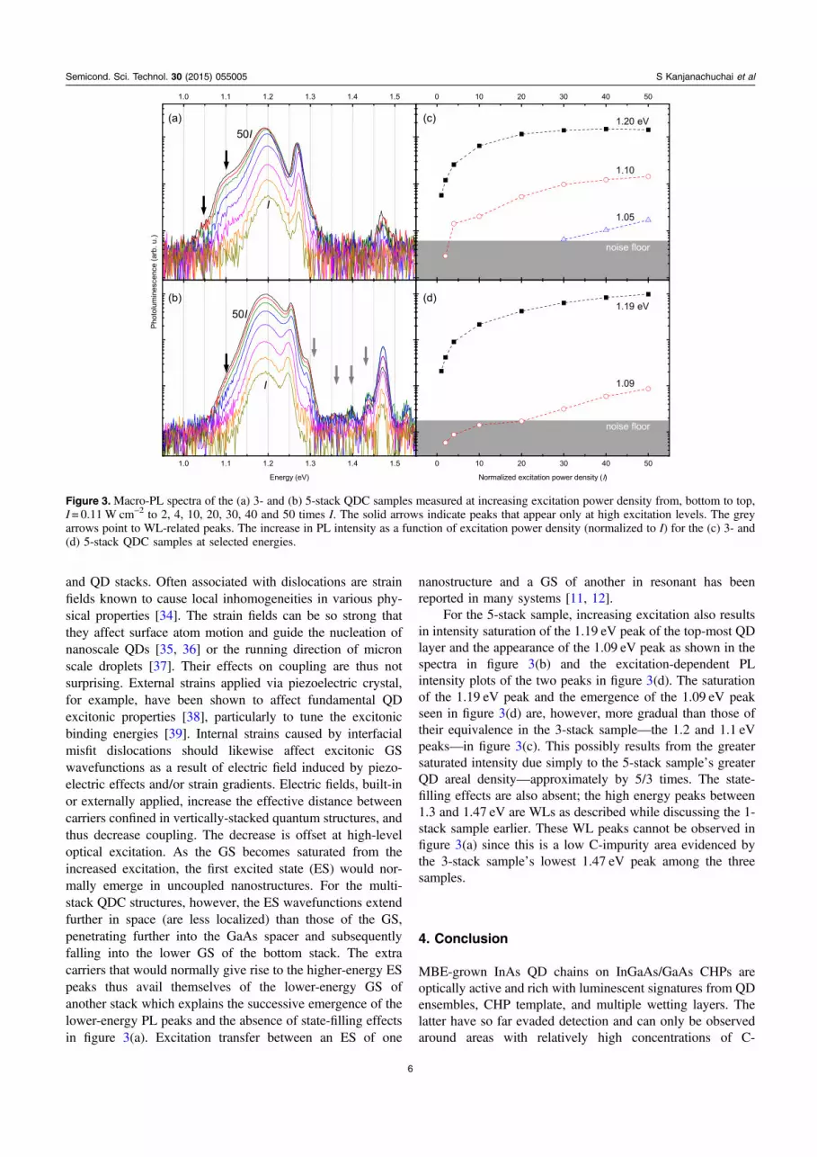
and QD stacks. Often associated with dislocations are strainfields known to cause local inhomogeneities in various phy-sical properties [34]. The strain fields can be so strong thatthey affect surface atom motion and guide the nucleation ofnanoscale QDs [35, 36] or the running direction of micronscale droplets [37]. Their effects on coupling are thus notsurprising. External strains applied via piezoelectric crystal,for example, have been shown to affect fundamental QDexcitonic properties [38], particularly to tune the excitonicbinding energies [39]. Internal strains caused by interfacialmisfit dislocations should likewise affect excitonic GSwavefunctions as a result of electric field induced by piezo-electric effects and/or strain gradients. Electric fields, built-inor externally applied, increase the effective distance betweencarriers confined in vertically-stacked quantum structures, andthus decrease coupling. The decrease is offset at high-leveloptical excitation. As the GS becomes saturated from theincreased excitation, the first excited state (ES) would nor-mally emerge in uncoupled nanostructures. For the multi-stack QDC structures, however, the ES wavefunctions extendfurther in space (are less localized) than those of the GS,penetrating further into the GaAs spacer and subsequentlyfalling into the lower GS of the bottom stack. The extracarriers that would normally give rise to the higher-energy ESpeaks thus avail themselves of the lower-energy GS ofanother stack which explains the successive emergence of thelower-energy PL peaks and the absence of state-filling effectsin figure 3(a). Excitation transfer between an ES of one
nanostructure and a GS of another in resonant has beenreported in many systems [11, 12].
For the 5-stack sample, increasing excitation also resultsin intensity saturation of the 1.19 eV peak of the top-most QDlayer and the appearance of the 1.09 eV peak as shown in thespectra in figure 3(b) and the excitation-dependent PLintensity plots of the two peaks in figure 3(d). The saturationof the 1.19 eV peak and the emergence of the 1.09 eV peakseen in figure 3(d) are, however, more gradual than those oftheir equivalence in the 3-stack sample—the 1.2 and 1.1 eVpeaks—in figure 3(c). This possibly results from the greatersaturated intensity due simply to the 5-stack sample’s greaterQD areal density—approximately by 5/3 times. The state-filling effects are also absent; the high energy peaks between1.3 and 1.47 eV are WLs as described while discussing the 1-stack sample earlier. These WL peaks cannot be observed infigure 3(a) since this is a low C-impurity area evidenced bythe 3-stack sample’s lowest 1.47 eV peak among the threesamples.
4. Conclusion
MBE-grown InAs QD chains on InGaAs/GaAs CHPs areoptically active and rich with luminescent signatures from QDensembles, CHP template, and multiple wetting layers. Thelatter have so far evaded detection and can only be observedaround areas with relatively high concentrations of C-
Figure 3. Macro-PL spectra of the (a) 3- and (b) 5-stack QDC samples measured at increasing excitation power density from, bottom to top,I= 0.11 W cm−2 to 2, 4, 10, 20, 30, 40 and 50 times I. The solid arrows indicate peaks that appear only at high excitation levels. The greyarrows point to WL-related peaks. The increase in PL intensity as a function of excitation power density (normalized to I) for the (c) 3- and(d) 5-stack QDC samples at selected energies.
6
Semicond. Sci. Technol. 30 (2015) 055005 S Kanjanachuchai et al
impurity evidenced from their co-occurrence with the 1.49 eVpeak. Based on this observation, we recommend that PLsignals should be optimized around a known impurity peak inorder to obtain a fuller picture of physics—albeit at theexpense of signal strength. When these InAs QD chains arestacked and separated by GaAs spacers, the top-most QDClayer dominates the emissions. The bottom-stack emissionsare however missing—an unexpected result from energeticconsideration since the bottom-stack QDs are the biggest andthus have the lowest energetic states. The missing emissionsare likely due to degraded bottom layer with increasingnumber of QDC layers and the non-coupling nature of theQDC stacks. Only by increasing excitation power densityuntil the top-most QDC layer is saturated do PL signaturesfrom the bottom layers appear—without state-filling effects inthe top-most QDC layer. The extended wavefunctions of theES are responsible for enhanced carrier tunnelling from thehigh-energy top layer to the low-energy bottom layer. Thisunique evolution of spectral changes with increased excitationpower can be used to identify carrier transfer among stacks ofdissimilar-sized nanostructures.
Acknowledgments
This work is supported by Thailand Research Fund(RSA5580015), Chulalongkorn University, the French Min-istère des affaires étrangères et européennes (MAEE) and theCentre National de la Recherche Scientifique (CNRS) throughthe STIC ASIA 2D nanotech project. SK would like to thankSuwat Sopitpan for technical assistance.
References
[1] Wasilewski Z R, Fafard S and McCaffrey J P 1999 J. Cryst.Growth 201-202 1131
[2] Inoue T, Asada M, Yasuoka N, Kojima O, Kita T and Wada O2010 Appl. Phys. Lett. 96 211906
[3] Solomon G S, Trezza J A, Marshall A F and Harris J J S 1996Phys. Rev. Lett. 76 952
[4] Cortez S, Krebs O, Laurent S, Senes M, Marie X, Voisin P,Ferreira R, Bastard G, Gérard J M and Amand T 2002 Phys.Rev. Lett. 89 207401
[5] Arakawa Y and Sakaki H 1982 Appl. Phys. Lett. 40 939[6] Luque A and Marti A 1997 Phys. Rev. Lett. 78 5014[7] Nozik A J, Beard M C, Luther J M, Law M, Ellingson R J and
Johnson J C 2010 Chem. Rev. 110 6873[8] Patanasemakul N, Panyakeow S and Kanjanachuchai S 2012
Nanoscale Res. Lett. 7 207[9] Le Ru E C, Howe P, Jones T S and Murray R 2003 Phys. Rev.
B 67 165303[10] Joyce P B, Le Ru E C, Krzyzewski T J, Bell G R,
Murray R and Jones T S 2002 Phys. Rev. B 66 075316[11] Heitz R, Mukhametzhanov I, Chen P and Madhukar A 1998
Phys. Rev. B 58 R10151
[12] Mazur Y I, Dorogan V G, Marega E, Zhuchenko Z Y,Ware M E, Benamara M, Tarasov G G, Vasa P,Lienau C and Salamo G J 2010 J. Appl. Phys. 108074316
[13] Schmidt O G 2007 Lateral Alignment of Epitaxial QuantumDots (Berlin: Springer)
[14] Kunets V P, Dias M R S, Rembert T, Ware M E, Mazur Y I,Lopez-Richard V, Mantooth H A, Marques G E andSalamo G J 2013 J. Appl. Phys. 113 183709
[15] Mazur Y I, Dorogan V G, Ware M E, Marega E, Lytvyn P M,Zhuchenko Z Y, Tarasov G G and Salamo G J 2012 J. Appl.Phys. 112 084314
[16] Chokamnuai T, Rattanadon P, Thainoi S, Panyakeow S andKanjanachuchai S 2013 J. Cryst. Growth 378 524
[17] Marzin J-Y, Gérard J-M, Izraël A, Barrier D and Bastard G1994 Phys. Rev. Lett. 73 716
[18] Seravalli L, Trevisi G and Frigeri P 2012 Cryst. Eng. Comm.14 6833
[19] Thongkamkoon N, Patanasemakul N, Siripitakchai N,Thainoi S, Panyakeow S and Kanjanachuchai S 2011J. Cryst. Growth 323 206
[20] Lee S J, Noh S K, Choe J W and Kim E K 2004 J. Cryst.Growth 267 405
[21] Lee H, Lowe-Webb R, Johnson T J, Yang W and Sercel P C1998 Appl. Phys. Lett. 73 3556
[22] Himwas C, Panyakeow S and Kanjanachuchai S 2011Nanoscale Res. Lett. 6 496
[23] Zhang C L, Wang Z G, Zhao F A, Xu B and Jin P 2004J. Cryst. Growth 265 60
[24] Xie Q, Madhukar A, Chen P and Kobayashi N P 1995 Phys.Rev. Lett. 75 2542
[25] Andrews A M, LeSar R, Kerner M A, Speck J S,Romanov A E, Kolesnikova A L, Bobeth M and Pompe W2004 J. Appl. Phys. 95 6032
[26] Pan D, Xu J, Towe E, Xu Q and Hsu J W 1998 Appl. Phys.Lett. 73 2164
[27] Kanjanachuchai S and Limwongse T 2011 J. Nanosci.Nanotechnol. 11 10787
[28] Limwongse T, Panyakeow S and Kanjanachuchai S 2009 Phys.Status Solidi C 6 806
[29] Welsch H, Kipp T, Köppen T, Heyn C and Hansen W 2008Semicond. Sci. Technol. 23 045016
[30] Wang X, Wang Z M, Liang B, Salamo G J and Shih C-K 2006Nano. Lett. 6 1847
[31] Yang T, Tatebayashi J, Aoki K, Nishioka M and Arakawa Y2007 Appl. Phys. Lett. 90 111912
[32] Akahane K and Yamamoto N 2011 J. Cryst. Growth 323154
[33] Laouthaiwattana K, Tangmattajittakul O, Suraprapapich S,Thainoi S, Changmuang P, Kanjanachuchai S,Ratanathamaphan S and Panyakeow S 2009 Sol. EnergyMater. Sol. Cells 93 746
[34] Freund L B and Suresh S 2006 Thin Film Materials: Stress,Defect Formation and Surface Evolution (Cambridge:Cambridge University Press)
[35] Shiryaev S Y, Jensen F, Hansen J L, Petersen J W andLarsen A N 1997 Phys. Rev. Lett. 78 503
[36] Xie Y H, Samavedam S B, Bulsara M, Langdo T A andFitzgerald E A 1997 Appl. Phys. Lett. 71 3567
[37] Kanjanachuchai S and Photongkam P 2015 Cryst. Growth Des.15 14
[38] Huo Y H et al 2014 Nat. Phys. 10 46[39] Ding F et al 2010 Phys. Rev. Lett. 104 067405
7
Semicond. Sci. Technol. 30 (2015) 055005 S Kanjanachuchai et al


