Embed Size (px)
Citation preview
ARTICLE IN PRESS
Physica B 404 (2009) 3684–3693
Contents lists available at ScienceDirect
Physica B
0921-45
doi:10.1
� Corr
E-m
(F. Ahm
journal homepage: www.elsevier.com/locate/physb
Half-metallicity characteristic at zincblende CrSb(0 0 1) surfaces and itsinterfaces with GaSb(0 0 1) and InAs(0 0 1)
F. Ahmadian a,�, M.R. Abolhassani a,b, M. Ghoranneviss a, M. Elahi a
a Plasma Physics Research Center, Science and Research Branch, Islamic Azad University, Tehran, Iranb Department of Physics, Tarbiat Modares University, Tehran, Iran
a r t i c l e i n f o
Article history:
Received 13 March 2009
Received in revised form
24 May 2009
Accepted 9 June 2009
PACS:
72.25.Mk
68.35.Md
75.70.�i
73.20.�r
31.15.E�
Keywords:
Spintronic
Half-metallicity
Surface
Interface
Density-functional theory
26/$ - see front matter & 2009 Elsevier B.V. A
016/j.physb.2009.06.059
esponding author. Tel.: +98 2144869627; fax
ail addresses: [email protected], m
adian).
a b s t r a c t
Electronic and magnetic properties of the zincblende CrSb(0 0 1) surfaces and its interfaces with
GaSb(0 0 1) and InAs(0 0 1) semiconductors are studied within the framework of the density-functional
theory using the FPLAPW+lo approach. We found that the Cr-terminated surfaces retain the half-
metallic character, while the half-metallicity is destroyed for the Sb-terminated surfaces due to surface
states, which originate from p electrons. The phase diagram obtained through the ab-initio atomistic
thermodynamics shows that at mCr � mbulkCr ffi 1:57 eV phase transition has occurred. Also the half-
metallicity character is preserved at both CrSb/GaSb and CrSb/InAs interfaces. The conduction band
minimum (CBM) of CrSb in the minority spin case lies about 0.63 eV above that of InAs, suggesting that
the majority spin can be injected into InAs without being flipped to the conduction bands of the
minority spin. On the other hand the CrSb/GaSb interface has a greater valence band offset (VBO)
compared with the CrSb/InAs interface and the minority electrons have lower contribution in
the injected currents and hence more efficient spin injection into the GaSb semiconductor. Thus the
CrSb/GaSb and CrSb/InAs heterojunctions can be useful in the field of spintronics.
& 2009 Elsevier B.V. All rights reserved.
1. Introduction
Half-metallic (HM) ferromagnets are the most desirable andappealing materials for spintronic devices. These materials haveone spin channel that is metallic, while the other spin channel hasa gap band at the Fermi level, which is known as the half-metallicband gap. Hence, 100% spin polarization of the conductingelectrons is expected from these materials. Since de Groot et al.[1] first predicted the HM property in half-Heusler alloys ofNiMnSb and PtMnSb, several HM ferromagnets such as rutilestructure CrO2 [2], double perovskite Sr2FeMoO6 [3], spinel Fe3O4
[4], pyrite-type CoS2 [5,6], Heusler alloy of Co2MnSi [7], and so onhave been theoretically predicted and experimentally synthesized.
Recently, many theoretical and experimental attempts havebeen done on the zinc blende (ZB) compounds such as MAs andMSb (M is a transition-metal element) [8–13], which arecompatible with III–V and II–VI semiconductors. It has already
ll rights reserved.
: +98 2144869640.
been established theoretically that the ZB MnAs phase is a ‘‘near-HM’’ ferromagnet because its HM gap is zero [14,15] and the ZBCrAs [10,16], the ZB MnSb, and ZB MnBi phases [17] are true HMferromagnets with finite HM gaps. So far only three ZB phaseshave been fabricated successfully. They are ZB MnAs in nanodots[9], ZB CrAs in thin films and multilayer [10,11], and ZB CrSb inthin films [12].
Later Liu [18] theoretically predicted that the ZB CrSb phase isa robust half-metallic ferromagnet with a magnetic moment of3.00mB per unit formula and its HM gap reaches 0.774 eV andpersists to be nonzero even when it is compressed by 21%.According to the results of B.-G. Lui, the ferromagnetic ZB phase ofCrSb is about 1 eV higher in total energy than the antiferromag-netic NiAs phase and therefore ZB CrSb should not exist as bulkcrystal, but can be grown as thin films epitaxially on III–Vsemiconductors [12]. So a practical approach for stabilizing theCrSb compound in the metastable ZB structure is the pseudo-morphic growth of CrSb thin films on ZB semiconductors. Thelattice parameter of ZB CrSb has been calculated to be equal to6.14 A [18], which has a negligible difference with the experi-mental lattice parameters of GaSb (6.1 A) and InAs (6.06 A)semiconductors. Therefore ZB CrSb might be grown on ZB

ARTICLE IN PRESS
Table 1Structural parameters of Cr-terminated and Sb-terminated slabs for both GaSb and
InAs lattice constants.
Surface h12 h23 h34 h45 h56 Bulk Surface energy
aGaSb
Cr termination 1.47 1.52 1.49 1.50 – 1.50 0.13
Sb termination 1.39 1.49 1.52 1.51 1.50 1.50 0.025
aInAs
Cr termination 1.49 1.53 1.52 1.52 – 1.52 0.13
Sb termination 1.4 1.49 1.55 1.54 1.54 1.52 0.024
The hij parameter is the interlayer distance of i and j layers in atomic unit (i and j
F. Ahmadian et al. / Physica B 404 (2009) 3684–3693 3685
semiconductors such as GaSb and InAs. But it is important forpractical applications whether or not the HM materials preservethe half-metallicity at surfaces and interfaces. In this paper, wehave theoretically investigated the HM behaviors on the (0 0 1)surfaces of CrSb and also CrSb/GaSb(0 0 1) and CrSb/InAs(0 0 1)interfaces.
The paper is organized as follows. After discussing thecomputational details in Section 2, the structural, electronic, andmagnetic properties of ZB CrSb(0 0 1) surfaces are presented inSection 3. Then we investigate the electronic and magneticproperties of the CrSb/GaSb and CrSb/InAs interfaces. The lastsection is devoted to the summary and conclusions.
are indexes of layers). The bulk values are given for comparison. Surface energy is
in Ry unit.
2. Computational method
We used the FPLAPW+lo method implemented in the WIEN2Kpackage [19] within the spin-polarized density-functional theory(DFT), for which the exchange-correlation energy of electrons isdescribed in the generalized gradient approximation (GGA) [20].Relativistic effects are taken into account within the scalarapproximation, neglecting the spin–orbit coupling. Basis func-tions, charge density, and potential are expanded inside mufin-tinspheres in combination with spherical harmonic functions with acut-off lmax ¼ 10, and in Fourier series in the interstitial region.Moreover, we used a parameter RMTKmax ¼ 8, which determinesthe matrix size (convergence), where Kmax is the plane wave cut-off and RMT the smallest of all atomic sphere radii. For all atoms,RMT was chosen as equal to 2.2 a.u. In all calculations we used an8�8�1 mesh for k-points in the Brillouin zone integration. Theself-consistent calculations are considered to be converged onlywhen the integrated charge difference per formula unit,Rjrn�rn�1jdr, between input charge density [rn�1(r)] and output
charge density [rn(r)] is less than 0.00001.
3. Results and discussions
3.1. Surface results
3.1.1. Structural properties
The ZB structure of CrSb in the [0 0 1] direction consists of twodifferent surfaces, Cr and Sb surfaces, with the alternatingsequence of ‘‘y/Cr/Sb/Cr/Sb/y’’. Furthermore, there are twopossible (0 0 1) terminations for CrSb, one is the Cr terminationand the other, the Sb termination surface. In our calculations thesesurface terminations consist of 9 atomic layers at the Crtermination, 11 atomic layers at the Sb termination, and 20 bohrvacuum thickness. The total energy of all supercells wasminimized by accurate relaxation of all atomic positions downto the force value of below 1 mRy/a.u.
In the first step we calculated the surface energies of differentsurfaces in the 2D lattice parameters of InAs (6.19 A) andGaSb (6.22 A). These values are listed in Table 1. Table 1values show that for both lattice constants the surface energy atthe Sb termination is lower than at the Cr termination andtherefore Sb termination surface is more stable than Crtermination surface.
In Table 1 we have also listed the interlayer distances for bothterminations. The comparison of interlayer distances in thesupercells and bulk is a good tool for studying interactionsbetween surface atoms. The values in Table 1 show that thedistance between surface and sub-surface layers (h12) at eachtermination has diminished with respect to bulk values. In bothterminations, Cr and Sb atoms on the surface lose two atoms oftheir four nearest neighbors and approximate to sub-surface
atoms to establish stronger bonds with sub-surface atoms.According to Table 1, by moving toward the center of slabs theinterlayer distances tend toward the corresponding value in thebulk case. This shows that at the center of the supercells thestructural properties of bulk at each termination are recovered.This result is good evidence for sufficient thickness of the Cr andSb termination slabs.
3.1.2. Electronic properties
In this section we will present the results of lattice parameterof only InAs, because the results of both lattice constants (aGaSb
and aInAs) are similar.The spin-resolved density of states (DOS) projected on the
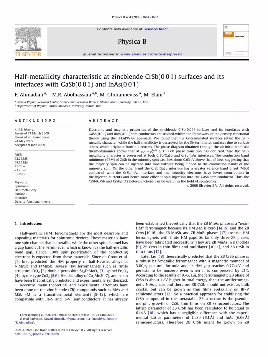
atomic orbitals at Cr-terminated surfaces are shown in Fig. 1. TheDOS’s of the surface and sub-surface atoms are compared to thebulk-like (the central atoms of supercell) cases. The Cr-terminatedsurfaces retain the HM nature of bulk CrSb but, however, there areimportant differences in the DOS of the Cr atom at the surface ascompared to the bulk-like case. The peaks at around �2.5 and�1 eV are reduced for the majority and minority spin cases,respectively. The Cr atom at the surface has lost two Sb neighborsand by losing two Sb p orbitals, the local peaks of the bondingstates of the Cr atom in these regions have been reduced. Butinstead the majority peak under the Fermi level has enhanced andcompensated the reduced bonding states in both spin directions.These results are completely similar to results obtained for theV surface atom at the (0 0 1) surfaces of VAs [21]. On the otherhand, by comparison between the DOS’s of surface and sub-surface atoms with bulk-like cases, we observe a relativebroadening in the �3.5 to �1.5 eV region for Cr d and Sb pstates in the case of surface and sub-surface atoms, respectively.This effect confirms the stronger bonds between sub-surface andsurface atoms that was previously mentioned.
It is also seen that in the 0 to �2 eV regions the electronicstates of the Cr surface atom at the spin majority case slightly shifttoward the Fermi level. These effects are mainly due to the surfacepotential that has been shown in Fig. 2. According to Fig. 2 thepotential at the surfaces of both terminations abruptly increasesand tends toward a fixed value. The abrupt increasing of thepotential at surface causes electronic states of the Cr atom to shifttoward the Fermi level. It is clear that the electronic states in thespin minority case have not been shifted by the surface potentialand so the half-metallicity character of the surface Cr atom hasbeen preserved.
For the Sb-terminated (0 0 1) surfaces the situation is com-pletely different from the Cr-terminated surfaces as can be seen inFig. 3. The DOS of the surface Sb atoms shows large deviationsfrom that of bulk-like Sb atoms. Such deviations were alsoobserved for As(0 0 1) and P(0 0 1) surfaces in CrAs and CrP,respectively [22,23]. As shown in Fig. 3, for the Sb-terminatedsurface, the HM character is destroyed due to the surface states
ARTICLE IN PRESS
DO
S (e
V/st
ates
)
0
5
10
15
20
Cr tot surface
Cr tot bulk-like
DO
S (e
V/st
ates
)
-0.2
-0.1
0.0
0.1
0.2Cr s surface
Cr s bulk-like
Energy (eV)-4
DO
S (e
V/st
ates
)
-4
-2
0
2
4
6
8
10
12
Cr d surface
Cr d bulk-like
-3
-2
-1
0
1
2
Sb tot sub surface
Sb tot bulk-like
-0.04
-0.02
0.00
0.02
0.04 Sb s sub surface
Sb s bulk-like
Energy (eV)-4
-1
0
1
Sb p sub surface
Sb p bulk-like
-3 -2 -1 0 1 2 -3 -2 -1 0 1 2
Fig. 1. Spin-resolved total and partial DOS’s of surface Cr and sub-surface Sb atoms at Cr-terminated (0 0 1) surface for InAs lattice constant. The surface DOS’s are compared
to those of the bulk-like atoms (dotted lines). Negative and positive numbers on the DOS axis represent the minority and majority spin states, respectively, and the Fermi
levels are set to zero.
F. Ahmadian et al. / Physica B 404 (2009) 3684–36933686
originating from the Sb surface atom, and are mainly due to Sbp states. The Sb atoms at Sb termination surface lose two of theirneighbors; therefore dangling bonds are created. It can be seenfrom Fig. 3 that these dangling bonds mainly have the character ofp orbitals and since the bands derived from p orbitals have alarger bandwidth than the d-bands, the electronic states of theSb atom at the surface can be extended to the HM band gap. Onthe other hand, by comparing the total electrostatic potential inboth terminations in Fig. 2, it can be clearly seen that the surfacepotential of the Sb termination is slightly higher than that ofCr termination and so it causes the electronic states of the Sb atomto be extended considerably to the HM band gap.
Comparing the DOS’s of Cr sub-surface and bulk-like atoms atthe Sb termination shows that the spin imbalance between themajority and minority states has decreased. A similar phenom-enon has been observed for Cr sub-surface atoms at the Astermination in the CrAs [22].
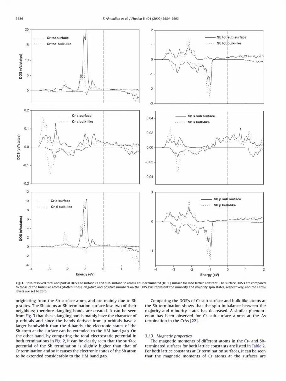
3.1.3. Magnetic properties
The magnetic moments of different atoms in the Cr- and Sb-terminated surfaces for both lattice constants are listed in Table 2.For both lattice constants at Cr termination surfaces, it can be seenthat the magnetic moments of Cr atoms at the surfaces are

ARTICLE IN PRESS
r (a.u.)0
V (R
y)
-0.9
-0.6
-0.3
0.0
0.3Cr terminationSb termination
10 20 30 40
Fig. 2. Total electrostatic potential profiles of the Cr termination and Sb
termination (0 0 1) surfaces. The horizontal axis is the length of supercell in
atomic unit.
F. Ahmadian et al. / Physica B 404 (2009) 3684–3693 3687
enhanced compared with those of the corresponding bulk-likevalues. Due to the reduced coordination number, Cr surface atomslose electron charge and their magnetic moment increases byapproximately 0.7mB. The magnetic moments of Sb sub-surfaceatoms have decreased by about 0.02mB. In the Sb termination, theenhancement of the magnetic moment in the Sb surface atoms isabout 0.03mB, while the magnetic moments of Cr sub-surfaceatoms have decreased by about 0.4mB. The noticeable reduction ofthe magnetic moment in the Cr sub-surface atom at the Sbtermination shows that the bonds between surface and sub-surface atoms are stronger than their similar bonds at Crtermination. These results are completely consistent with thevalues in Table 1, where the distances between surface and sub-surface layers (h12) at Sb termination are smaller than the Crtermination slab.
3.1.4. Phase diagram
Our calculations in this section present the relative stability ofthe different surfaces for the case of the InAs lattice constantwithin the framework of ab-initio atomistic thermodynamics[24,25]. In this scheme, the surface free energy used to assess thestability of different terminations is defined as follow:
gðT; PiÞ ¼ ½GðT ; PiÞ �X
i
NimiðT; PiÞ�
,2A (1)
Here G is the Gibbs free energy of the surface, Ni and mi are thenumber and the chemical potential of the ith element, respec-tively, 2A is the total surface area of the symmetrical supercell,and g the surface free energy per area. By calculating andcomparing the surface free energies of different terminationsversus reasonable values of the chemical potentials, we can findthe most stable surface having the lowest surface free energy forany given values of chemical potentials. All results of thiscomparison could be offered as a phase diagram. Clearly twochemical potentials (mCr and mSb) are involved in the CrSb surfacefree energies (Eq. (1)). The appropriate thickness of the supercellsshows that the surfaces are in thermodynamic equilibrium withthe central bulk layers and imposes the following equilibriumcondition to the chemical potentials:
mCr þ mSb ¼ gCrSbbulk (2)
where gCrSbbulk is the Gibbs free energy of the bulk CrSb. This
equation reduces the number of independent chemical potentialsof Eq. (1) to one.
The Gibbs free energy has two important parts: the static totalenergy that comes out of the DFT calculations and the vibrationalenergy. It is obtained that at sufficiently low temperatures thevibrational contributions can be neglected [25] and the DFT totalenergies are enough for surface free energy calculations. Further-more, the surface free energies of both terminations can bewritten as follows:
2AgCr-termination ¼ �0:05 Ry� mCr (3)
2AgSb-termination ¼ 0:36 Ryþ mCr (4)
In Fig. 4 the surface free energies for both terminations areplotted versus the chemical potential of the Cr atom. As expected,in the small values of mCr the Sb termination surface is stable; byincreasing mCr, the energy difference of the two terminations isreduced and finally with the occurrence of phase transition atmCr � mbulk
Cr ffi 1:57 eV, Cr termination is stabled.In practice, the phase diagram obtained from the surface free
energies is valid only within a limited range of the chemicalpotentials because over-increasing or -decreasing these parametersmay lead to the decomposition of the alloy. For example if mCr
becomes too low then the Cr atoms prefer to leave the sample andbulk Sb (at rhombohedral structure) will form. Hence the lowerlimit of mCr is determined by the Gibbs free energy of bulk Sb:
mminCr þ gSb
bulk ¼ gCrSbbulk (5)
where gSbbulk and gCrSb
bulkare the Gibs free energies of bulk Sb and CrSb,respectively.
The maximum value of mCr can be obtained from the Gibs freeenergy of Cr bulk (in the bcc structure):
gCrbulk ¼ mmax
Cr (6)
The formation energy of ZB CrSb was found to be positive (about0.1 Ry); therefore ZB CrSb is an unstable structure, which is notformed in equilibrium conditions. This result is in agreement witha recent report [18]. This implies that the lower limit of mCr islarger than the higher limit of mCr, leaving no thermodynamicallyaccessible region in our phase diagram. These observationsindicate that both Cr and Sb terminations are not stable inequilibrium conditions and non-equilibrium growth techniquesare required for realizing these surface terminations.
3.2. Interface results
As previously implied, InAs and GaSb semiconductors with ZBstable structure are promising candidates for CrSb growth becauseof their close lattice matching to ZB CrSb. However, there are smallmismatches between ZB CrSb and both GaSb and InAs semi-conductors and a small strain is imposed at the interface whenCrSb is deposited to InAs(0 0 1) and GaSb(0 0 1) substrates. To findout the optimized structure of CrSb on each GaSb and InAssubstrates we fixed the 2D (in plane) lattice constant of CrSb equalto the calculated lattice constants of GaSb and InAs semiconduc-tors and by establishing the tetragonal unit cell we relaxed thelattice parameter in the growth direction to minimize the totalenergy. The obtained lattice parameters (in the growth direction)of CrSb are 6 and 6.08 A for GaSb and InAs substrates, respectively.In order to construct the interface between CrSb and both GaSband InAs semiconductors, we used the supercell approach; inparticular, tests performed as a function of the cell dimensionshave shown that bulk conditions at both sides of the interfacewere well recovered using two slabs with 7 and 9 layers, one7-layer slab for CrSb(0 0 1) and a 9-layer slab for each of theGaSb(0 0 1) and InAs(0 0 1) substrates. We have also optimized theinterfacial distance parameter (the spacing between substrate and

ARTICLE IN PRESS
DO
S (s
tate
s/eV
)
-2
-1
0
1
2
Sb tot surfaceSb tot bulk-like
DO
S (s
tate
s/eV
)
-0.02
0.00
0.02
0.04 Sb s surfaceSb s bulk-like
Energy (eV)-4
DO
S (s
tate
s/eV
)
-2
-1
0
1Sb p surfaceSb p bulk-like
-2
0
2
4
6
8
Cr tot sub surfaceCr tot bulk-like
-0.2
-0.1
0.0
0.1
0.2
0.3
Cr s sub surfaceCr s bulk-like
Energy (eV)
-2
0
2
4
6
8
Cr d sub surfaceCr d bulk-like
-3 -2 -1 0 1 2 -4 -3 -2 -1 0 1 2
Fig. 3. Spin-resolved total and partial DOS’s of surface Sb and sub-surface Cr atoms at Sb-terminated (0 0 1) surfaces for InAs lattice constant. The surface DOS’s are
compared to those of the bulk-like atoms (dotted lines). Negative and positive numbers on the DOS axis represent the minority and majority spin states, respectively, and
the Fermi levels are set to zero.
F. Ahmadian et al. / Physica B 404 (2009) 3684–36933688
film) by testing different values of this parameter and letting theatoms move along the [0 0 1] direction to minimize simulta-neously the forces on the atoms and the total energy. Forconstructing the type of junction we were encountered withdifferent selections, but here we have presented only the moststable junctions. The investigated junctions for CrSb/GaSb andCrSb/InAs heterojunctions are ‘‘y/Ga/Sb/Cr/y’’ and ‘‘y/In/As/Cr/y’’, respectively.
In order to study and compare the stability of both interfaces,we initially calculated the formation energies by comparing the
fully minimized total energies of the interface supercells withbulk GaSb, InAs, and CrSb energies. For the remaining non-stoichiometric atoms in the supercells, the bulk energies of As, Sb,and Cr crystals were used (corresponding to mAs ¼ mbulk
As ,mSb ¼ mbulk
Sb , and mCr ¼ mbulkCr ). The obtained formation energies
are 0.1 and 0.42 Ry for CrSb/GaSb and CrSb/InAs supercells,respectively. So, the CrSb/GaSb interface is more stable thanthe CrSb/InAs interface. In the following, electronic andmagnetic properties of both interfaces have been separatelyinvestigated.
ARTICLE IN PRESS
Table 2Spin magnetic moments in mB for the surface and sub-surface layers in the case of
Cr- and Sb-terminated (0 0 1) surfaces for both GaSb and InAs lattice constants.
Cr terminated
Cr (surface) Sb (sub-surface) Cr (bulk-like) Sb (bulk-like)
aGaSb 3.8 �0.2 3.1 �0.22
aInAs 3.8 �0.2 3.1 �0.22
Sb terminated
Sb (surface) Cr (sub-surface) Cr (bulk-like) Sb (bulk-like)
aGaSb �0.25 2.7 3.08 �0.22
aInAs �0.25 2.7 3.08 �0.22
The bulk-like (the central atoms of supercell) values are given for comparison.
μμCr (Ry)-0.40
γ (R
y)
-0.2
0.0
0.2
0.4
Cr terminationSb termination
phase transition
-0.35 -0.30 -0.25 -0.20 -0.15
Fig. 4. Phase diagram of the two ideal terminations of CrSb(0 0 1).
DO
S (s
tate
s/eV
)
-2
0
2
4
6 Cr d ( top interface)
Cr d (film center)
DO
S (s
tate
s/eV
)
-1.0
-0.5
0.0
0.5
1.0
Sb p (interface)
Sb p (film center)
Sb p (substrate center)
Energy (eV)-4
DO
S (s
tate
s/eV
)
-0.2
-0.1
0.0
0.1
0.2
Ga p (sub interface)
Ga p (substrate center)
-3 -2 -1 0 1 2
Fig. 5. Spin-resolved partial DOS’s of Cr (at top interface), Sb (at interface), and Ga (at
sub-interface) atoms in the CrSb/GaSb heterojunction. The majority and minority
states are plotted upward and downward, respectively. Dotted lines correspond to
bulk-like (film center or substrate center) partial DOS. The Fermi energy is set to zero.
F. Ahmadian et al. / Physica B 404 (2009) 3684–3693 3689
3.2.1. Electronic and magnetic properties
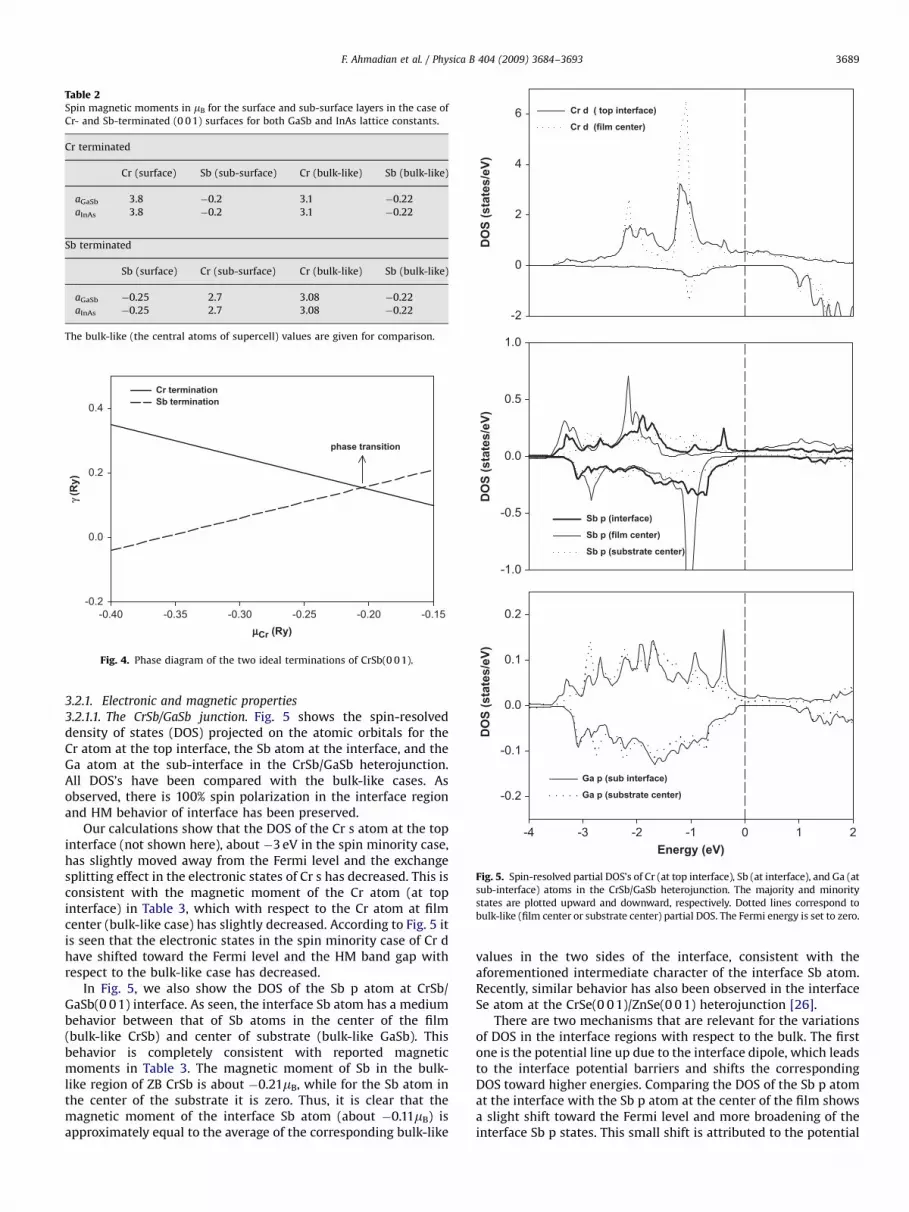
3.2.1.1. The CrSb/GaSb junction. Fig. 5 shows the spin-resolveddensity of states (DOS) projected on the atomic orbitals for theCr atom at the top interface, the Sb atom at the interface, and theGa atom at the sub-interface in the CrSb/GaSb heterojunction.All DOS’s have been compared with the bulk-like cases. Asobserved, there is 100% spin polarization in the interface regionand HM behavior of interface has been preserved.
Our calculations show that the DOS of the Cr s atom at the topinterface (not shown here), about �3 eV in the spin minority case,has slightly moved away from the Fermi level and the exchangesplitting effect in the electronic states of Cr s has decreased. This isconsistent with the magnetic moment of the Cr atom (at topinterface) in Table 3, which with respect to the Cr atom at filmcenter (bulk-like case) has slightly decreased. According to Fig. 5 itis seen that the electronic states in the spin minority case of Cr dhave shifted toward the Fermi level and the HM band gap withrespect to the bulk-like case has decreased.
In Fig. 5, we also show the DOS of the Sb p atom at CrSb/GaSb(0 0 1) interface. As seen, the interface Sb atom has a mediumbehavior between that of Sb atoms in the center of the film(bulk-like CrSb) and center of substrate (bulk-like GaSb). Thisbehavior is completely consistent with reported magneticmoments in Table 3. The magnetic moment of Sb in the bulk-like region of ZB CrSb is about �0.21mB, while for the Sb atom inthe center of the substrate it is zero. Thus, it is clear that themagnetic moment of the interface Sb atom (about �0.11mB) isapproximately equal to the average of the corresponding bulk-like
values in the two sides of the interface, consistent with theaforementioned intermediate character of the interface Sb atom.Recently, similar behavior has also been observed in the interfaceSe atom at the CrSe(0 0 1)/ZnSe(0 0 1) heterojunction [26].
There are two mechanisms that are relevant for the variationsof DOS in the interface regions with respect to the bulk. The firstone is the potential line up due to the interface dipole, which leadsto the interface potential barriers and shifts the correspondingDOS toward higher energies. Comparing the DOS of the Sb p atomat the interface with the Sb p atom at the center of the film showsa slight shift toward the Fermi level and more broadening of theinterface Sb p states. This small shift is attributed to the potential

ARTICLE IN PRESS
Table 3Spin magnetic moments in mB for top interface, interface, and sub-interface atoms at CrSb/GaSb (0 0 1) and CrSb/InAs (0 0 1) heterojunctions.
CrSb/GaSb CrSb/InAs
Atom Position Magnetic moment Atom Position Magnetic moment
Cr Top interface 3.05 In Sub-interface 0.01
Cr Film center 3.11 In Substrate center 0
Sb Interface �0.11 As Interface �0.13
Sb Substrate center 0 As Substrate center 0
Sb Film center �0.21 Cr Top interface 3
Ga Sub-interface 0 Cr Film center 3.16
Ga Substrate center 0 – – –
The bulk-like (film center or substrate center) values are given for comparison.
r (a.u.)0 5 10 15 20 25
V (R
y)
-1.6
-1.4
-1.2
CrSb/GaSb
r (a.u.)5 10 15 20 25
-1.6
-1.4
-1.2
CrSb/InAs
CrSb
GaSb InAs CrSb
Fig. 6. Total electrostatic potential profiles of the CrSb/GaSb(0 0 1) and CrSb/InAs(0 0 1) heterojunctions. The horizontal axis is the length of supercell in atomic unit.
F. Ahmadian et al. / Physica B 404 (2009) 3684–36933690
raise-up at the interface, which is shown in Fig. 6. It is clear fromFig. 6 that the total electrostatic potential around the interface hasabruptly increased. The second one is the exchange splittingeffect, which is relative to the splitting between the minority andmajority DOS’s. As seen from Fig. 5 the exchange splitting in theDOS of the Sb p atom at interface with respect to central atoms ofthe film and the substrate has decreased and increased,respectively. These changes in the exchange splitting of theinterface Sb atom are expectable, because the p states of theinterface Sb atom hybridize with neighboring Cr d states on oneside (accompanied by observed exchange splitting in the bulkCrSb [18]) and with neighboring Ga s and p states on the otherside (without exchange splitting similar to bulk GaSb).
Finally, by generally looking at the DOS of the Ga p atom atsub-interface, it is clearly observed that the potential raise-up hasaffected the electronic states of Ga p and slightly moved themtoward the Fermi level. Also, the presence of significant electronicstates in the spin majority case at the Fermi level shows that theHM character of interface Sb atom has been transferred to the Gaatom at the sub-interface.
3.2.1.2. The CrSb/InAs junction. Our results on the local DOS ofthree atoms around CrSb/InAs junction have been presented inFig. 7. According to Fig. 7 no interface states are formed within theHM gap at the CrSb/InAs interface and the half-metallicitycharacter is conserved throughout.
Comparing the DOS of the In p atom at sub-interface with theIn p atom at the center of the substrate (bulk-like case) shows that
the spin majority states at the Fermi level have increased anddestroyed the balance between the spin majority and minoritystates of the In atom in the bulk-like case. This result confirms thereported magnetic moment value in Table 3 of the In atom in thesub-interface to be about 0.01mB.
The DOS of the As p atom in the interface of CrSb/InAs showsthat the exchange splitting effect is more dominant with respectto the interface potential raise-up effect (the total electrostaticpotential is shown in Fig. 6). In the CrSb/InAs heterojunction eachinterface As atom has two In neighbors on one side, and twoCr neighbors on the other side. The p–d hybridization betweenCr and As on one side (similar to CrAs bulk [22]), preserves thespin minority gap at the Fermi level, and the exchange splitting isstill present. The magnetic moment of about �0.13mB attributed tothe As atom in Table 3 is smaller than that of the bulk case (about�0.38mB). The considerable reduction of magnetic moment of theinterface As atom with respect to the bulk case is due to its havingan intermediate role between film and substrate. This behavior issimilar to the interface Sb atom in the CrSb/GaSb supercell.
The DOS of the Cr d atom at top interface shows that theexchange splitting effect has slightly decreased with respect to theCr d atom in the center of the film and this result confirms thepresented magnetic moment of the Cr atom in Table 3, which isabout 0.16 smaller than that of the Cr atom at the film center.
3.2.1.3. Band alignment. Finally we extracted the spin-resolvedband alignments as a technologically relevant quantity for theelectronic and spintronic properties of layered devices. In general

ARTICLE IN PRESS
DO
S (s
tate
s/eV
)
-0.1
0.0
0.1In p (sub interface)In p (substrate center)
DO
S (s
tate
s/eV
)
-0.6
-0.3
0.0
0.3
As p (interface)As p (substrate center)
Energy (eV)-6
DO
S (s
tate
s/eV
)
0
3
6
Cr d (top interface)Cr d (film center)
-4 -2 0 2
Fig. 7. Spin-resolved partial DOS’s of Cr (at top interface), As (at interface), and In
(at sub-interface) atoms in the CrSb/InAs heterojunction. The majority and
minority states are plotted upward and downward, respectively. Dotted lines
correspond to bulk-like (film center or substrate center) partial DOS. The Fermi
energy is set to zero.
F. Ahmadian et al. / Physica B 404 (2009) 3684–3693 3691
the half-metal/semiconductor heterojunction for the majorityspin resembles a metal–semiconductor contact with a p- orn-type Schottky barrier (Fp, Fn) while in the minority channel theinterface acts as a semiconductor/semiconductor heterojunctionand the band discontinuities are defined as valence and conduc-tion band offsets (VBO, CBO).
As indicated in Fig. 8 Fp (Fn) is defined as the differencebetween semiconductor valence band maximum—VBM(conduction band minimum—CBM) and metal Fermi level whileVBO (CBO) is the difference between minority half-metal VBM(CBM) and semiconductor VBM (CBM). In order to calculate theband alignment parameters we follow the well-established ‘‘bulkplus line up’’ procedure in which the bulk band structures are
combined with a potential line-up parameter obtained frominterface slab calculations. The potential line-up at CrSb/GaSb andCrSb/InAs heterojunctions is determined by comparing theelectronic structure of the core electrons in the bulk andinterface central layers. According to this procedure, thepotential line-up parameter is defined as DEbulk
s �DEslabs , where
DEbulks and DEslab
s are the energy differences of Cr 1s and Ga 1s (orCr 1s and In 1s) core electrons in the bulk compounds and slabcentral layers, respectively. A similar approach has been employedfor the calculation of valence band offset (VBO) in GaAs/AlAs [27].The obtained potential line-ups for CrSb/GaSb and CrSb/InAssupercells are 0.08 and 0.07 eV, respectively. By applying thesepotential line-ups, we aligned and separately matched thecalculated bulk band structures of CrSb with GaSb and that ofCrSb with InAs, to determine the band diagram of the CrSb/GaSband CrSb/InAs heterojunctions. The band alignment profiles areschematically shown in Fig. 8. Since GGA approximationunderestimates the band gaps of semiconductors, we shifted upthe conduction bands (CBs) of GaSb and InAs to match theexperimental band gaps (0.726 and 0.354 eV, respectively) inthe band alignments. The obtained band alignment parameters inthe CrSb/GaSb(0 0 1) and CrSb/InAs(0 0 1) heterojunctions arelisted in Table 4. The calculated value of Fn for CrSb/GaSb(0 0 1)is in good agreement with the reported value in recent work(0.89 eV) [28]. As observed of Fig. 8, in both interfaces the Fermilevel of CrSb lies below the CBM of GaSb and InAs semiconductors.This suggests that a Schottky barrier can be formed for n-GaSb orn-InAs and a reverse bias should be applied to allow majority spinto tunnel into GaSb or InAs semiconductors. In the CrSb/InAsinterface the CBM of minority spin in the CrSb lies at about0.63 eV above the CBM of InAs and so the majority spin electronscan be directly injected to n-InAs with less probability of beingflipped to the CBs of the minority spin under the applied reversebias. This suggests the possibility of highly efficient spin injection.
On the other hand the CrSb/GaSb heterojunction has a greaterVBO compared with the CrSb/InAs heterojunction. This may beevidence for the lower contribution of minority electrons in theinjected currents and hence more efficient spin injection into theGaSb semiconductor. Therefore both GaSb and InAs semiconduc-tors are promising and suitable substrates for the injection ofefficient spin polarization current of ZB CrSb.
4. Conclusion
We employed density-functional calculations to investigatethe structural, electronic, and magnetic properties of ZB CrSb(0 0 1) surfaces and ZB CrSb(0 0 1) interfaces with GaAs(0 0 1) andInAs(0 0 1) semiconductors. The results show that the Sb termina-tion surface of CrSb(0 0 1) is more stable than the Cr terminationsurface while the CrSb/GaSb interface was found to be more stablethan the CrSb/InAs interface. It was found that Cr-terminatedsurfaces are HM, whereas the HM nature is destroyed for the Sb-terminated surface due to surface states in the minority band. Themagnetic moments of the surface Cr (Sb) atoms were found to beenhanced by 0.7mB (0.03mB) at the Cr termination (Sb termina-tion), whereas the magnetic moments of the sub-surface Cr (Sb)atoms were reduced by 0.3mB (0.02mB) at the Sb termination(Cr termination). The obtained phase diagram shows that the Crand Sb termination surfaces are not theoretically stable andprobably such surfaces can be grown using non-equilibriumgrowth methods. Results of our calculations confirm that CrSbretains HM behavior at the CrSb/GaSb and CrSb/InAs interfaces.The DOS of Sb and As interface atoms in the CrSb/GaSb andCrSb/InAs heterojunctions, respectively, show an intermediatebehavior in comparison with central atoms of film and substrate.

ARTICLE IN PRESS
Ener
gy (e
V)
-1
0
1
GaSb CrSbgrowth direction
Fermi level of CrSb
GaSb-CBM
GaSb-VBM
CrSb-CBM
CrSb-VBM
Ener
gy (e
V)
-1
0
1
InAs CrSbgrowth direction
Fermi level of CrSbInAs-CBM
InAs-VBM
CrSb-CBM
CrSb-VBM
CBO
VBO
CBO
VBO
Φn
Φp
Φn
Φp
Fig. 8. Schematic band diagram in the CrSb/GaSb(0 0 1) and CrSb/InAs(0 0 1) heterojunctions. The Fermi energy of CrSb is set to zero.
Table 4Calculated band offsets and Schottky barrier heights in [0 0 1] direction of CrSb/
GaSb(0 0 1) and CrSb/InAs(0 0 1) heterojunctions.
Heterojunction Fn Fp VBO CBO
CrSb/GaSb 0.76 0.04 0.96 0.002
CrSb/InAs 0.14 0.35 0.54 0.63
All parameters are in eV unit.
F. Ahmadian et al. / Physica B 404 (2009) 3684–36933692
The calculated band alignment at CrSb/InAs heterojunction showsthe possibility of directly injecting majority spins into thesemiconductor with less possibility of being flipped to the CBsof the minority spin of CrSb. Also CrSb/GaSb heterojunction has agreater VBO compared with CrSb/InAs heterojunction and theprobability of injecting the minority spins of CrSb into GaSb is lessthan the probability of their being injected into InAs. These resultssuggest that the CrSb/GaSb and CrSb/InAs heterojunctions aresuitable candidates in the field of spintronics.
Acknowledgments
The authors would like to thank the Computational Nanotech-nology Supercomputing Center, Institute for Research in Funda-mental Sciences (IPM), P.O. Box 19395-5531, Tehran, Iran, for theirsupport and supercomputing facilities. F. Ahmadian gratefullyappreciates Dr. S.J. Hashemifar for helpful discussions.
References
[1] R.A. de Groot, F.M. Mueller, P.G. van Engen, K.H.J. Buschow, Phys. Rev. Lett. 50(1983) 2024.
[2] K. Schwarz, J. Phys. F 16 (1986) L211.[3] K.-I. Kobayashi, T. Kimura, H. Sawada, K. Terakura, Y. Tokura, Nature (London)
392 (1998) 677.[4] W.C. Kim, K. Kawaguchi, N. Koshizaki, M. Sohma, T. Matsumoto, J. Appl. Phys.
93 (2003) 8032.[5] R. Yamamoto, A. Machida, Y. Moritomo, A. Nakamura, Phys. Rev. B 59 (1999)
R7793.[6] T. Shishidou, A.J. Freeman, R. Asahi, Phys. Rev. B 64 (2001) R180401.[7] S. Ishida, T. Masaki, S. Fujii, S. Asano, Physica B 245 (1998) 1.
ARTICLE IN PRESS
F. Ahmadian et al. / Physica B 404 (2009) 3684–3693 3693
[8] T. Plake, M. Ramsteiner, V.M. Kaganer, B. Jenichen, M. Kastner, L. Daweritz,K.H. Ploog, Appl. Phys. Lett. 80 (2002) 2523;S. Sugahara, M. Tanaka, Appl. Phys. Lett. 80 (2002) 1969.
[9] K. Ono, J. Okabayashi, M. Mizuguchi, M. Oshima, A. Fujimori, H. Akinaga,J. Appl. Phys. 91 (2002) 8088.
[10] H. Akinaga, T. Manago, M. Shirai, Jpn. J. Appl. Phys. 39 (2000) L1118.[11] M. Mizuguchi, H. Akinaga, T. Manago, K. Ono, M. Oshima, M. Shirai, M. Yuri,
H.J. Lin, H.H. Hsieh, C.T. Chen, J. Appl. Phys. 91 (2002) 7917.[12] J.H. Zhao, F. Matsukura, K. Takamura, E. Abe, D. Chiba, H. Ohno, Appl. Phys.
Lett. 79 (2001) 2776.[13] P. Radhakrishna, J.W. Cable, Phys. Rev. B 54 (1996) 11940.[14] S. Sanvito, N.A. Hill, Phys. Rev. B 62 (2000) 15 553.[15] A. Continenza, S. Picozzi, W.T. Geng, A.J. Freeman, Phys. Rev. B 64 (2001)
085204;Y.J. Zhao, W.T. Geng, A.J. Freeman, B. Delley, Phys. Rev. B 65 (2002) 113202.
[16] M. Shirai, Physica E (Amsterdam) 10 (2000) 147;I. Galanakis, Phys. Rev. B 66 (2002) 012406.
[17] Y.-Q. Xu, B.-G. Liu, D.G. Pettifor, Phys. Rev. B 66 (2002) 184435.[18] B.-G. Liu, Phys. Rev. B 67 (2003) 172411.[19] P. Blaha, K. Schwarz, J. Luitz, WIEN2k, 2001, Wien2k, Vienna University of
Technology, 2002, improved and updated Unix version of the originalcopyrighted Wien-code, which was published by P. Blaha, K. Schwarz,P. Sorantin, S.B. Trickey, Comput.Phys.Commun.59 (1990) 399, ISBN 3-9501031-1-2.
[20] J. Perdew, K. Burke, M. Ernzerhof, Phys. Rev. Lett. 77 (1996) 3865.[21] I. Galanakis, P. Mavropoulos, Phys. Rev. B 67 (2003) 104417.[22] I. Galanakis, Phys. Rev. B 66 (2002) 012406.[23] G. Rahman, S. Cho, S.C. Hong, J. Magn, Magn. Mater 310 (2007) 2192.[24] G.X. Qian, R.M. Martin, D.J. Chadi, Phys. Rev. B 38 (1988) 7649.[25] K. Reuter, M. Scheffler, Phys. Rev. B 65 (2001) 035406.[26] E. Hazrati, S.J. Hashemifar, H. Akbarzadeh, J. Appl. Phys. 104 (2008)
113719.[27] S. Massidda, B.I. Min, A.J. Freeman, Phys. Rev. B 35 (1987) 9871.[28] R.Q. Wu, L. Liu, G.W. Peng, Y.P. Feng, J. Appl. Phys. 99 (2006) 093703.
![Optical constants of Ga[sub 1−x]In[sub x]As[sub y]Sb[sub 1−y] lattice matched to GaSb (001): Experiment and modeling](https://img.dokumen.tips/doc/110x75/635219899ff726561f09513c/optical-constants-of-gasub-1xinsub-xassub-ysbsub-1y-lattice-matched.jpg)


