Embed Size (px)
Citation preview
F
MPa
b
c
a
ARRAA
KAHA
1
maaofiedct[sooowoa
0d
Electrochimica Acta 54 (2009) 1070–1075
Contents lists available at ScienceDirect
Electrochimica Acta
journa l homepage: www.e lsev ier .com/ locate /e lec tac ta
ormation of anodic films on sputtering-deposited Al–Hf alloys
. Fogazzaa, M. Santamariaa, F. Di Quartoa, S.J. Garcia-Vergarab, I. Molchanb,. Skeldonb,∗, G.E. Thompsonb, H. Habazakic
Dipartimento di Ingegneria Chimica dei Processi et dei Materiali, Università di Palermo, Viale delle Scienze, Palermo 90128, ItalyCorrosion and Protection Centre, School of Materials, The University of Manchester, P.O. Box 88, Manchester M60 1QD, UKGraduate School of Engineering, Hokkaido University, Sapporo 060-8628, Japan
r t i c l e i n f o
rticle history:eceived 4 July 2008eceived in revised form 7 August 2008ccepted 28 August 2008vailable online 4 September 2008
eywords:luminiumafniumnodic oxidation
a b s t r a c t
The growth of barrier-type anodic films at high efficiency on a range of sputtering-deposited Al–Hf alloys,containing from 1 to 95 at.% Hf, has been investigated in ammonium pentaborate electrolyte. The alloysencompassed nanocrystalline and amorphous structures, the latter being produced for alloys containingfrom 26 to 61 at.% Hf. Except at the highest hafnium content, the films were amorphous and contained unitsof HfO2 and Al2O3 distributed relatively uniformly through the film thickness. Boron species were confinedto outer regions of the films. The boron distributions suggest that the cation transport number decreasesprogressively with increasing hafnium concentration in the films, from ∼0.4 in anodic alumina to ∼0.2 fora film on an Al–61 at.% Hf alloy. The distributions of Al3+ and Hf4+ ions in the films indicate their similarmigration rates, which correlates with the similarity of the energies of Al3+–O2− and Hf4+–O2− bonds.
For an alloy containing ∼95 at.% Hf, the film was largely nanocrystalline, with a thin layer of amorphousoxide, of non-uniform thickness, at the film surface. The formation ratios for the films on the alloys changedapproximately in proportion to the hafnium content of the films between the values for anodic aluminad 1.8
iomssiwm[be
ptos
and anodic hafnia, ∼1.2 an
. Introduction
Studies of barrier-type anodic films formed on binary alu-inium alloys are useful for understanding the influences of
lloying elements during anodizing of commercial aluminiumlloys. The resulting oxides, which incorporate units of aluminiumxide and alloying element oxide [1,2], usually in an amorphouslm structure, are also of interest for investigation of band gapnergies in “mixed” oxides [3]. They may also be of practical valueue to their controllable dielectric constants. The oxides generallyomprise single- or bi-layers depending upon the relative migra-ion rates of the aluminium and alloying element ions in the oxide4–6]. Similar migration rates of the two cation species lead toingle-layered oxides, while differing migration rates result in anuter layer of the oxide of the faster migrating cation species. Thexides may also contain regions incorporating low concentrations
f species derived from the anions in the electrolyte [7,8]. The out-ard migration of the cations is accompanied by inward migrationf oxygen species [9]. Thus, the films form both at the metal/filmnd film/electrolyte interfaces and at the boundary between the∗ Corresponding author. Tel.: +44 161 306 4872; fax: +44 161 306 4826.E-mail address: [email protected] (P. Skeldon).
da
2
mT
013-4686/$ – see front matter © 2008 Elsevier Ltd. All rights reserved.oi:10.1016/j.electacta.2008.08.052
nm V−1 respectively.© 2008 Elsevier Ltd. All rights reserved.
nner and outer layers of layered films. The relative migration ratesf the cation species usually show a dependence on the singleetal–oxygen bond energies of the constituent oxide units, with
pecies of high bond energy relative to Al3+–O2− migrating morelowly than Al3+ ions and vice versa [10,11]. Enrichment of the alloy-ng element immediately beneath the oxide film may also occur
hen the Gibbs free energy of formation per equivalent for for-ation of the alloying element oxide is higher than that of alumina
6]. For alloys containing a sufficient level of alloying element in theulk alloy, enrichment is not required for oxidation of the alloyinglement to proceed.
The present study investigates film formation on Al–Hf alloysrepared by magnetron sputtering. The primary interest here lies inhe compositions of the anodic films and the migration behavioursf Al3+ and Hf4+ ions. The films may also be of interest as dielectrics,ince hafnium oxide has attracted attention as a ‘high-K’ gateielectric in metal oxide semiconductor transistors [12] and hafniadditions to alumina increase the dielectric constant [13–15].
. Experimental
Al–Hf alloys were deposited by magnetron sputtering onto alu-inium substrates, of dimensions 2.0 cm × 1.5 cm, using an Atom
ech System, with targets of 99.999% aluminium (Cu 0.3 ppm, Fe
imica Acta 54 (2009) 1070–1075 1071
0CN2btrtawssD∼scv0rca
amat
Foi
V
FA
M. Fogazza et al. / Electroch
.3 ppm, Mg 1.2 ppm, Si 0.8 ppm) and 97.0% hafnium (Al 30 ppm,r < 50 ppm, Cu < 50 ppm, Fe 100 ppm, Mg < 10 ppm, Mo < 10 ppm,b < 50 ppm, Ta < 100 ppm, Ti 25 ppm, U 0.5 ppm, W < 50 ppm, Zr.8%, C 30 ppm, N 10 ppm). The aluminium substrates, which hadeen first electropolished and then anodized to form a 180 nm-hick barrier oxide films, were attached to a copper table thatotated beneath the targets. Deposition conditions were selectedo provide alloys containing 1, 12, 26, 40, 54, 61, 95 at.% Hf. Thelloy thicknesses were ∼350 nm. Layers of aluminium and hafniumere also prepared, using the previous individual targets. The
puttering chamber was typically evacuated to ∼2 × 10⁻⁵ Pa, withputtering subsequently carried out in 99.999% argon at ∼0.5 Pa.uring deposition, the temperature of the copper table reached303 K. Specimens were also prepared from 99.99% aluminium
heet that was electropolished for 180 s in 20%/80% (by vol.) per-hloric acid/ethanol at less than 278 K. Following masking, thearious specimens were then anodized to 150 V at 5 mA cm−2 in.1 M ammonium pentaborate electrolyte at 293 K. Voltage–timeesponses were recorded during anodizing. Six specimens of eachomposition of material were individually anodized, with the aver-ge slope determined for the voltage–time response.
Ultramicrotomed sections of the deposited layers, prior tond following anodizing, were examined by transmission electronicroscopy (TEM), in a JEOL FX 2000 II instrument. Compositions of
lloys and anodic films were determined by Rutherford backscat-ering spectroscopy (RBS), using 2.0 MeV He+ ions produced by the
dwbta
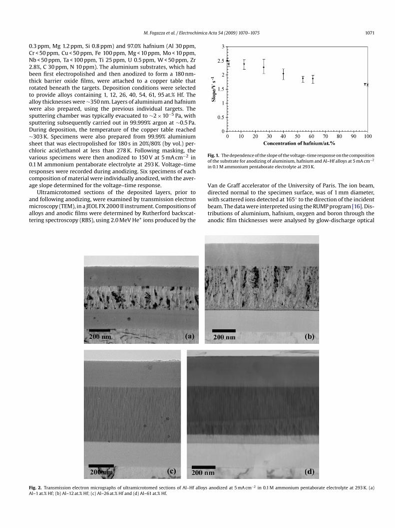
ig. 2. Transmission electron micrographs of ultramicrotomed sections of Al–Hf alloysl–1 at.% Hf; (b) Al–12 at.% Hf; (c) Al–26 at.% Hf and (d) Al–61 at.% Hf.
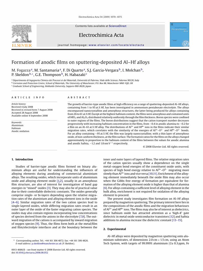
ig. 1. The dependence of the slope of the voltage–time response on the compositionf the substrate for anodizing of aluminium, hafnium and Al–Hf alloys at 5 mA cm−2
n 0.1 M ammonium pentaborate electrolyte at 293 K.
an de Graff accelerator of the University of Paris. The ion beam,irected normal to the specimen surface, was of 1 mm diameter,
ith scattered ions detected at 165◦ to the direction of the incidenteam. The data were interpreted using the RUMP program [16]. Dis-ributions of aluminium, hafnium, oxygen and boron through thenodic film thicknesses were analysed by glow-discharge optical
anodized at 5 mA cm−2 in 0.1 M ammonium pentaborate electrolyte at 293 K. (a)
1072 M. Fogazza et al. / Electrochimica Acta 54 (2009) 1070–1075
F 5 at.%e
eYgcrdt2
3
aomtnaftlacfamtipnctFtfii[
strftewlaF∼
compositions comprising units of Al2O3 and HfO2 in proportion tothe atomic ratio of Al/Hf in the substrate; typical spectra are shownin Fig. 5. Efficiencies of close to 100% were indicated by the chargeof the cations in the film compared with the charge passed duringanodizing (Table 1). The relatively uniform presence of aluminium
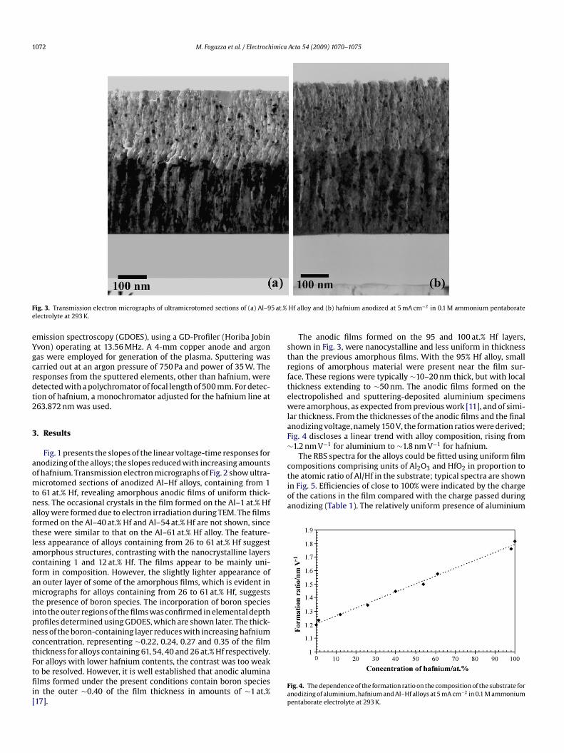
ig. 3. Transmission electron micrographs of ultramicrotomed sections of (a) Al–9lectrolyte at 293 K.
mission spectroscopy (GDOES), using a GD-Profiler (Horiba Jobinvon) operating at 13.56 MHz. A 4-mm copper anode and argonas were employed for generation of the plasma. Sputtering wasarried out at an argon pressure of 750 Pa and power of 35 W. Theesponses from the sputtered elements, other than hafnium, wereetected with a polychromator of focal length of 500 mm. For detec-ion of hafnium, a monochromator adjusted for the hafnium line at63.872 nm was used.
. Results
Fig. 1 presents the slopes of the linear voltage-time responses fornodizing of the alloys; the slopes reduced with increasing amountsf hafnium. Transmission electron micrographs of Fig. 2 show ultra-icrotomed sections of anodized Al–Hf alloys, containing from 1
o 61 at.% Hf, revealing amorphous anodic films of uniform thick-ess. The occasional crystals in the film formed on the Al–1 at.% Hflloy were formed due to electron irradiation during TEM. The filmsormed on the Al–40 at.% Hf and Al–54 at.% Hf are not shown, sincehese were similar to that on the Al–61 at.% Hf alloy. The feature-ess appearance of alloys containing from 26 to 61 at.% Hf suggestmorphous structures, contrasting with the nanocrystalline layersontaining 1 and 12 at.% Hf. The films appear to be mainly uni-orm in composition. However, the slightly lighter appearance ofn outer layer of some of the amorphous films, which is evident inicrographs for alloys containing from 26 to 61 at.% Hf, suggests
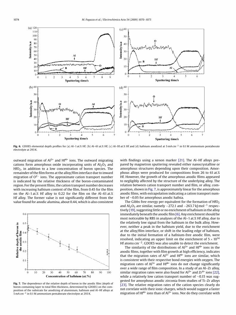
he presence of boron species. The incorporation of boron speciesnto the outer regions of the films was confirmed in elemental depthrofiles determined using GDOES, which are shown later. The thick-ess of the boron-containing layer reduces with increasing hafniumoncentration, representing ∼0.22, 0.24, 0.27 and 0.35 of the filmhickness for alloys containing 61, 54, 40 and 26 at.% Hf respectively.
or alloys with lower hafnium contents, the contrast was too weako be resolved. However, it is well established that anodic aluminalms formed under the present conditions contain boron speciesn the outer ∼0.40 of the film thickness in amounts of ∼1 at.%17].
Fap
Hf alloy and (b) hafnium anodized at 5 mA cm−2 in 0.1 M ammonium pentaborate
The anodic films formed on the 95 and 100 at.% Hf layers,hown in Fig. 3, were nanocystalline and less uniform in thicknesshan the previous amorphous films. With the 95% Hf alloy, smallegions of amorphous material were present near the film sur-ace. These regions were typically ∼10–20 nm thick, but with localhickness extending to ∼50 nm. The anodic films formed on thelectropolished and sputtering-deposited aluminium specimensere amorphous, as expected from previous work [11], and of simi-
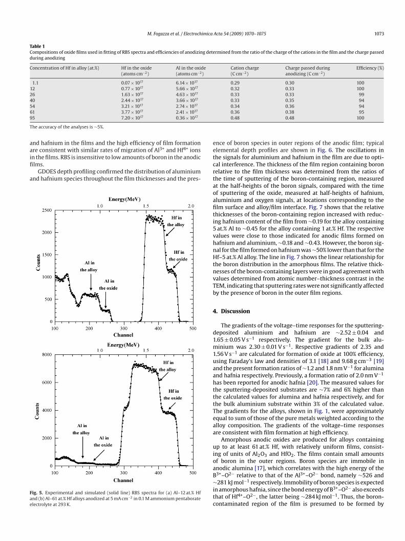
ar thickness. From the thicknesses of the anodic films and the finalnodizing voltage, namely 150 V, the formation ratios were derived;ig. 4 discloses a linear trend with alloy composition, rising from1.2 nm V−1 for aluminium to ∼1.8 nm V−1 for hafnium.
The RBS spectra for the alloys could be fitted using uniform film
ig. 4. The dependence of the formation ratio on the composition of the substrate fornodizing of aluminium, hafnium and Al–Hf alloys at 5 mA cm−2 in 0.1 M ammoniumentaborate electrolyte at 293 K.
M. Fogazza et al. / Electrochimica Acta 54 (2009) 1070–1075 1073
Table 1Compositions of oxide films used in fitting of RBS spectra and efficiencies of anodizing determined from the ratio of the charge of the cations in the film and the charge passedduring anodizing
Concentration of Hf in alloy (at.%) Hf in the oxide(atoms cm−2)
Al in the oxide(atoms cm−2)
Cation charge(C cm−2)
Charge passed duringanodizing (C cm−2)
Efficiency (%)
1.1 0.07 × 10¹⁷ 6.14 × 10¹⁷ 0.29 0.30 10012 0.77 × 10¹⁷ 5.66 × 10¹⁷ 0.32 0.33 10026 1.63 × 10¹⁷ 4.63 × 10¹⁷ 0.33 0.33 9940 2.44 × 10¹⁷ 3.66 × 10¹⁷ 0.33 0.35 9454 3.21 × 10¹⁷ 2.74 × 10¹⁷ 0.34 0.36 9469
T
aaifi
a
Fae
ee
1 3.77 × 10¹⁷ 2.41 × 10¹⁷
5 7.20 × 10¹⁷ 0.36 × 10¹⁷
he accuracy of the analyses is ∼5%.
nd hafnium in the films and the high efficiency of film formationre consistent with similar rates of migration of Al3+ and Hf4+ ions
n the films. RBS is insensitive to low amounts of boron in the anodiclms.GDOES depth profiling confirmed the distribution of aluminiumnd hafnium species throughout the film thicknesses and the pres-
ig. 5. Experimental and simulated (solid line) RBS spectra for (a) Al–12 at.% Hfnd (b) Al–61 at.% Hf alloys anodized at 5 mA cm−2 in 0.1 M ammonium pentaboratelectrolyte at 293 K.
tcrtaoafiti5vhnHtnvTb
4
d1m1uaahtttTeaa
uioaB∼itc
0.36 0.38 950.48 0.48 100
nce of boron species in outer regions of the anodic film; typicallemental depth profiles are shown in Fig. 6. The oscillations inhe signals for aluminium and hafnium in the film are due to opti-al interference. The thickness of the film region containing boronelative to the film thickness was determined from the ratios ofhe time of sputtering of the boron-containing region, measuredt the half-heights of the boron signals, compared with the timef sputtering of the oxide, measured at half-heights of hafnium,luminium and oxygen signals, at locations corresponding to thelm surface and alloy/film interface. Fig. 7 shows that the relativehicknesses of the boron-containing region increased with reduc-ng hafnium content of the film from ∼0.19 for the alloy containingat.% Al to ∼0.45 for the alloy containing 1 at.% Hf. The respectivealues were close to those indicated for anodic films formed onafnium and aluminium, ∼0.18 and ∼0.43. However, the boron sig-al for the film formed on hafnium was ∼50% lower than that for thef–5 at.% Al alloy. The line in Fig. 7 shows the linear relationship for
he boron distribution in the amorphous films. The relative thick-esses of the boron-containing layers were in good agreement withalues determined from atomic number–thickness contrast in theEM, indicating that sputtering rates were not significantly affectedy the presence of boron in the outer film regions.
. Discussion
The gradients of the voltage–time responses for the sputtering-eposited aluminium and hafnium are ∼2.52 ± 0.04 and.65 ± 0.05 V s−1 respectively. The gradient for the bulk alu-inium was 2.30 ± 0.01 V s−1. Respective gradients of 2.35 and
.56 V s−1 are calculated for formation of oxide at 100% efficiency,sing Faraday’s law and densities of 3.1 [18] and 9.68 g cm−3 [19]nd the present formation ratios of ∼1.2 and 1.8 nm V−1 for aluminand hafnia respectively. Previously, a formation ratio of 2.0 nm V−1
as been reported for anodic hafnia [20]. The measured values forhe sputtering-deposited substrates are ∼7% and 6% higher thanhe calculated values for alumina and hafnia respectively, and forhe bulk aluminium substrate within 3% of the calculated value.he gradients for the alloys, shown in Fig. 1, were approximatelyqual to sum of those of the pure metals weighted according to thelloy composition. The gradients of the voltage–time responsesre consistent with film formation at high efficiency.
Amorphous anodic oxides are produced for alloys containingp to at least 61 at.% Hf, with relatively uniform films, consist-
ng of units of Al2O3 and HfO2. The films contain small amountsf boron in the outer regions. Boron species are immobile innodic alumina [17], which correlates with the high energy of the
3+–O2− relative to that of the Al3+–O2− bond, namely ∼526 and281 kJ mol−1 respectively. Immobility of boron species is expectedn amorphous hafnia, since the bond energy of B3+–O2− also exceedshat of Hf4+–O2−, the latter being ∼284 kJ mol−1. Thus, the boron-ontaminated region of the film is presumed to be formed by
1074 M. Fogazza et al. / Electrochimica Acta 54 (2009) 1070–1075
F Al–95e
ocHrmirwoHv
Fbp5
wpapHtr
ig. 6. GDOES elemental depth profiles for (a) Al–1 at.% Hf; (b) Al–61 at.% Hf; (c)lectrolyte at 293 K.
utward migration of Al3+ and Hf4+ ions. The outward migratingations form amorphous oxide incorporating units of Al2O3 andfO2, in addition to a low concentration of boron species. The
emainder of the film forms at the alloy/film interface due to inwardigration of O2− ions. The approximate cation transport number
s indicated by the relative thickness of the boron-contaminatedegion. For the present films, the cation transport number decreases
ith increasing hafnium content of the film, from 0.45 for the filmn the Al–1 at.% Hf alloy to 0.22 for the film on the Al–61 at.%f alloy. The former value is not significantly different from thealue found for anodic alumina, about 0.44, which is also consistent
ig. 7. The dependence of the relative depth of boron in the anodic film (depth oforon-containing layer to total film thickness, determined by GDOES) on the com-osition of the substrate for anodizing of aluminium, hafnium and Al–Hf alloys atmA cm−2 in 0.1 M ammonium pentaborate electrolyte at 293 K.
pab
atimteadrH
atimoswg[nm
at.% Hf and (d) hafnium anodized at 5 mA cm−2 in 0.1 M ammonium pentaborate
ith findings using a xenon marker [21]. The Al–Hf alloys pre-ared by magnetron sputtering revealed either nanocrystalline ormorphous structures depending upon their composition. Amor-hous alloys were produced for compositions from 26 to 61 at.%f. However, the growth of the amorphous anodic films appeared
o negligibly affected by the structure of the underlying alloy. Theelation between cation transport number and film, or alloy, com-osition, shown in Fig. 7, is approximately linear for the amorphousnodic films, with extrapolation indicating a cation transport num-er of ∼0.05 for amorphous anodic hafnia.
The Gibbs free energy per equivalent for the formation of HfO2nd Al2O3 are similar, namely −272.1 and −263.7 kJ mol−1 respec-ively [19], suggesting little or no enrichment of hafnium in the alloymmediately beneath the anodic film [6]. Any enrichment should be
ost noticeable by RBS in analyses of the Al–1 at.% Hf alloy, due tohe relatively low signal from the hafnium in the bulk alloy. How-ver, neither a peak in the hafnium yield, due to the enrichmentt the alloy/film interface, or shift in the leading edge of hafnium,ue to the initial formation of a hafnium-free anodic film, wereesolved, indicating an upper limit on the enrichment of 5 × 10¹⁴
f atoms cm−2. GDOES was also unable to detect the enrichment.The similarity of the distributions of Al3+ and Hf4+ ions in the
nodic films, together with film growth at high efficiency, indicateshat the migration rates of Al3+ and Hf4+ ions are similar, whichs consistent with their respective bond energies with oxygen. The
igration rates of Al3+ and Hf4+ ions do not change significantlyver a wide range of film composition. In a study of an Al–Zr alloy,imilar migration rates were also found for Al3+ and Zr4+ ions [22],
hile a relatively low cation transport number of ∼0.15 was sug-ested for amorphous anodic zirconia from studies of Ti–Zr alloys23]. The relative migration rates of the cation species clearly doot correlate with their ionic charges, which would suggest a fasterigration of Hf4+ ions than of Al3+ ions. Nor do they correlate with
imica
i0fpi[so
watm[bHotaudromtoaifintioAg
5
5ctlafil
oacia
ctiash
A
Rti
R
[
[
[
[
[[
[[[
[
[[[
[
M. Fogazza et al. / Electroch
onic radii of Al3+ and Hf4+ ions, with respective values of 0.39 and.58 nm for four-fold co-ordination and 0.535 and 0.71 nm for six-old co-ordination. Various models of ionic migration have beenroposed ranging from early suggestions of vacancy diffusion and
nterstitial exchange capture [24] to a liquid-droplet mechanism25] that allows for counter-migration of anions and cations withimilar transport number. A more recent model links the migrationf cations to structural relaxation around oxygen vacancies [26].
The anodic films formed on hafnium and the Al–95 at.% Hf alloy,ere nanocrystalline. However, the film on the latter contained
morphous regions at the film surface. In common with nanocrys-alline zirconia, nanocrystalline hafnia forms primarily by inward
igration of O2− ions, with a cation transport number of <0.0527]. Thus, anodic hafnia forms largely at the metal/film interfacey transport of oxygen along short-circuit paths through the oxide.owever, for the Al–95 at.% Hf alloy, initial formation of amorphousxide is suggested, followed by transition to growth of nanocrys-alline material. The initially formed amorphous oxide remainst the film surface. The amorphous region extends to depths ofp to ∼0.18 of the film thickness, which is similar to the depthistribution of boron determined by GDOES. Boron species mayeside primarily in the amorphous regions, since the film formedn hafnium in which amorphous oxide was not resolved containeduch less boron. For the mainly nanocrystalline films, the distribu-
ion of boron may therefore not be an indicator of the proportionf film growth due to cation transport. Ionic transport within themorphous layer is presumed to supply oxygen ions to the underly-ng hafnium-rich oxide. In studies of Ti–Zr alloys, amorphous anodiclms underwent a structural transition for sufficiently high zirco-ium contents, with ∼63 at.% Zr promoting generation of nanocrys-als of zirconia [23]. The nanocrystals were distributed within thenner, mainly amorphous, layer formed due to inward migrationf O2− ions. A similar type of mixed film structure may arise forl–Hf alloys for compositions between 61 and 95 at.% Hf, prior toeneration of the nanocrystalline oxide of high hafnium content.
. Conclusions
Anodic films formed on sputtering-deposited Al–Hf alloys atmA cm−2 in 0.1 M ammonium pentaborate electrolyte at 293 Komprise units of Al2O3 and HfO2 distributed throughout the filmhickness. The films are amorphous on alloys containing up to ateast 61 at.% Hf, with transition to mainly nanocrystalline materialt high hafnium contents. The growth of the amorphous anodiclms appeared to negligibly affected by the structure of the under-
ying alloy.The relative uniformity of the composition of the amorphous
2−
xides is consistent with growth by inward migration of O ionsnd outward migration of Al3+ and Hf4+ ions at similar rates. Theation transport number in the amorphous oxides reduces withncrease of hafnium content. For high hafnium contents, the filmsre nanocrystalline.[[[[
Acta 54 (2009) 1070–1075 1075
The formation ratios increased linearly with increasing hafniumontent of the anodic films, from 1.2 nm V−1 for anodic aluminao 1.8 nm V−1 for anodic hafnia. The transport number of cationsn the amorphous films also shows a linear trend from ∼0.4 forlumina to ∼0.2 for the film on an Al–61 at.% Hf alloy. Extrapolationuggests a cation transport number of ∼0.05 in amorphous anodicafnia.
cknowledgements
The authors are grateful to the Engineering and Physical Sciencesesearch Council (U.K.) for support of this work. They also wish tohank Dr I. Vickridge, Universités Paris 7 et 6, for assistance withon beam analyses.
eferences
[1] K. Sasaki, T. Umezawa, Thin Solid Films 74 (1980) 83.[2] V. Labunov, V. Sokol, A. Vorobiova, V. Bondarenko, Electrochim. Acta 30 (1985)
1079.[3] N.T.C. Oliveira, S.R. Biaggio, S. Piazza, C. Sunseri, F. Di Quarto, Electrochim. Acta
49 (2004) 4563.[4] H. Habazaki, K. Shimizu, P. Skeldon, G.E. Thompson, G.C. Wood, J. Mater. Res. 12
(1997) 1885.[5] H. Habazaki, K. Shimizu, P. Skeldon, G.E. Thompson, G.C. Wood, J. Electrochem.
Soc. 143 (1996) 2465.[6] H. Habazaki, K. Shimizu, P. Skeldon, G.E. Thompson, G.C. Wood, X. Zhou, Trans.
Inst. Met. Finish. 75 (1997) 18.[7] H. Takahashi, K. Fujimoto, M. Nagayama, J. Electrochem. Soc. 135 (1988)
1349.[8] H. Konno, S. Kobayashi, H. Takahashi, M. Nagayama, Electrochim. Acta 25 (1980)
1667.[9] L. Iglesias-Rubianes, P. Skeldon, G.E. Thompson, H. Habazaki, K. Shimizu, Corros.
Sci. 45 (2003) 2905.10] G. Alcala, S. Mato, P. Skeldon, G.E. Thompson, K. Shimizu, H. Habazaki, Corros.
Sci. 45 (2003) 1803.11] H. Habazaki, K. Shimizu, P. Skeldon, G.E. Thompson, G.C. Wood, Corros. Sci. 43
(2001) 1393.12] Y.H. Kim, J.C.-Y. Lee, J.C. Lee, S. Banerjee, Hf-based High-k Dielectrics: Process
Development, Morgan & Claypool, 2005.13] H.Y. Yu, M.F. Li, B.J. Cho, C.C. Yeo, M.S. Joo, D.-L. Kwong, J.S. Pan, C.H. Ang, J.Z.
Zheng, S. Ramanathan, Appl. Phys. Lett. 81 (2002) 376.14] J. Petry, W. Vandervorst, T. Conard, Mater. Sci. Eng. B 109 (2004) 56.15] O. Buiu, Y. Lu, S. Hall, I.Z. Mitrovic, R.J. Potter, P.R. Chalker, Thin Solid Films 515
(2007) 3772.16] L.R. Doolittle, Nucl. Instrum. Methods B9 (1985) 344.17] K. Shimizu, G.E. Thompson, G.C. Wood, Thin Solid Films 85 (1981) 53.18] P. Skeldon, K. Shimizu, G.E. Thompson, G.C. Wood, Surf. Interface Anal. 5 (1983)
247.19] D.R. Lide, Handbook of Physics and Chemistry, 78th ed., CRC Press, Boca Raton,
NY, 1997–1998.20] M.T. Thomas, J. Electrochem. Soc. 117 (1970) 396.21] F. Brown, W.D. Mackintosh, J. Electrochem. Soc. 120 (1973) 1096.22] H. Habazaki, P. Skeldon, K. Shimizu, G.E. Thompson, G.C. Wood, J. Phys. D 28
(1995) 2612.23] H. Habazaki, M. Uozumi, H. Konno, K. Shimizu, S. Nagata, K. Asami, K. Mat-
sumoto, K. Takayama, Y. Oda, P. Skeldon, G.E. Thompson, Electrochim. Acta 28
(2003) 3257.24] G. Amsel, D. Samuel, J. Phys. Chem. Solids 23 (1962) 1707.25] N.F. Mott, Philos. Mag. B 55 (1987) 117.26] M.-H. Wang, K.R. Hebert, J. Electrochem. Soc. 146 (1999) 3741.27] J.A. Davies, B. Domeij, J.P.S. Pringle, S. Brown, J. Electrochem. Soc. 112 (1965)
675.


