Embed Size (px)
Citation preview
INSTITUTE OF PHYSICS PUBLISHING JOURNAL OF MICROMECHANICS AND MICROENGINEERING
J. Micromech. Microeng. 17 (2007) 26–35 doi:10.1088/0960-1317/17/1/004
Fabrication of vertical mirrors usingplasma etch and KOH:IPA polishingR Agarwal1, S Samson2 and S Bhansali1
1 Department of Electrical Engineering, University of South Florida, Tampa, FL 33620, USA2 College of Marine Science, University of South Florida, St Petersburg, FL 33773, USA
E-mail: [email protected], [email protected] and [email protected]
Received 20 July 2006, in final form 10 October 2006Published 30 November 2006Online at stacks.iop.org/JMM/17/26
AbstractA new approach to etch structures with vertical sidewalls in Si is presentedin this paper. This process reduces the loading effect in deep reactive ionetching (DRIE) and maintains a uniform etch profile and etch ratethroughout the wafer. Shallow areas were patterned under the regions to beremoved. The wafer was then bonded to a pyrex wafer which acts as ahandle wafer and as a package lid for packaging MEMS devices. Uniformwidth narrow channels encompassing these shallow patterns were thensubjected to long through wafer DRIE. These narrow channels maintainuniform etch rates while patterning structures with various fill factors on thesame wafer. Various structures were etched with vertical side walls acrossthe 550 µm thick Si wafer. Average side wall angles of 89.8◦ were obtainedwith just 0.3◦ variation across the 4′′ Si wafer. The process showedresistance to slight variations in DRIE parameters with a negligible effect onthe sidewall profile. Additionally, the verticality of the structures wasimproved to 90.08◦ by performing KOH:IPA wet etching on the plasmaetched surfaces. Once characterized, the same processes can be used forvarious shape/size structures. These etched vertical mirrors were used toassemble a corner cube retroreflector.
(Some figures in this article are in colour only in the electronic version)
1. Introduction
Three-dimensional (3D) structures can be etched into orcreated on a Si substrate by bulk micromachining or by surfacemicromachining, respectively. The inherent nature of bulkmicromachining leads to three-dimensional structures in thebulk of Si [1], whereas surface micromachined parts can berotated [2] or popped up [3] to assemble three-dimensionalstructures. Vertical mirrors are the necessary components foroptical corner cube retroreflector communicators (CCRs) anda variety of other optical devices, such as external cavity lasers,filters, and resonators, capacitive accelerometers and opticalcross connects, etc. Various processes such as anisotropicwet etching, LIGA process or DRIE can be used to achievevertical structures. Vertical structures with atomically smoothsurfaces [4–6] can be etched in Si by wet anisotropic etchingof Si on a (1 1 0) wafer with the mask aligned to the (1 1 1)crystal plane. Various devices such as accelerometers [7], beam
splitters [4] and comb structures [8] have been realized usingvertical structures etched in the (1 1 0) Si wafer, but the shape ofstructures which can be realized using wet anisotropic etchingis highly restricted by the crystallography of the silicon wafer.For example, while it is possible to wet etch vertical mirrorsusing (1 1 0) Si, structures in the shape of cross-hairs are notpossible to fabricate as the (1 1 1) planes intersect at an angleof 70.53◦ to the (1 1 0) plane. The LIGA process [9] can beused to fabricate vertical metallic or polymer microstructuresor molds, but requires expensive x-ray exposure which is notcommon in most facilities. DRIE techniques can allow etchingof extremely complex geometries, but have loading-dependentetch characteristics and rougher sidewalls. Extensive researchhas been done to characterize geometric effects on etch rates;large open areas and small trenches etch at different rates andproduce different amounts of lateral etching [10].
Maintaining a vertical etch profile for through waferetches has been an important area of research in MEMS. It
0960-1317/07/010026+10$30.00 © 2007 IOP Publishing Ltd Printed in the UK 26
Fabrication of vertical mirrors using plasma etch and KOH:IPA polishing
is difficult to maintain a vertical etch profile during long DRIEruns as the etch profile depends highly on etching patternsand plasma conditions [11]. Efforts to realize extremelyvertical sidewalls using various methods to overcome themicro loading in DRIE continue to be an active area ofinvestigation [12–16]. A model to etch vertical structures wasdemonstrated by Jansen et al [12]. They used the black silicon(continuous monitoring of the etched surface was done untilit turns black) method to determine optimum etch parameters.As continuous monitoring is required to determine the rightprocess parameters, this method was not feasible for batchfabrication. Bertz et al [13] used a fusion bonded maskedSi wafer to etch vertical structures in a Si substrate. Thismasking wafer was first etched using wet anisotropic etchingto define the masks for the device wafer. This anisotropic wetetching of the masking wafer limited the structures that couldbe realized using DRIE in this method. In the method usedby Ikehara et al [14], vertical structures were first defined byetching deep trenches around the structures. To maintain theverticality, uniform width trenches were used. The remainingareas were then removed by successive DRIE. Since spraycoating photoresist was used to pattern the high topographystructures, the vertical structures defined by first DRIE etchwere found to be damaged around the sharp corners becauseof the non-uniform coating of the masking photoresist. Twolong DRIE etches along with lithography on high topographystructures were used to maintain the vertical profile duringthe long DRIE etches. Hsieh et al [15] described the use ofguarding walls where many uniform width stripes were definedin the peripheral of the main structures. DRIE was performedin three different steps and lithography was performed on hightopographies. Finally the guarding walls were released usingwet etching. Contour lithography [16] was demonstratedto fabricate vertical structures in nano and micro domainsin the same wafer. Mita et al introduced the concept ofcontour lithography using two different lithography steps andsubsequent DRIE to negotiate the loading effect in DRIE whileetching high aspect ratio features.
These previous methods use multiple long DRIE stepsand/or multiple lithography steps on high topographystructures were performed. To overcome these limitationsa new 2-step DRIE process is described here, where the deepRIE was performed only once to etch thought the 550 µmthick Si wafer, along with one short DRIE. While simplelithography steps were employed, the unwanted Si blockswere released automatically without the use of any etchantand vertical structures were fabricated with an incorporatedpackage lid.
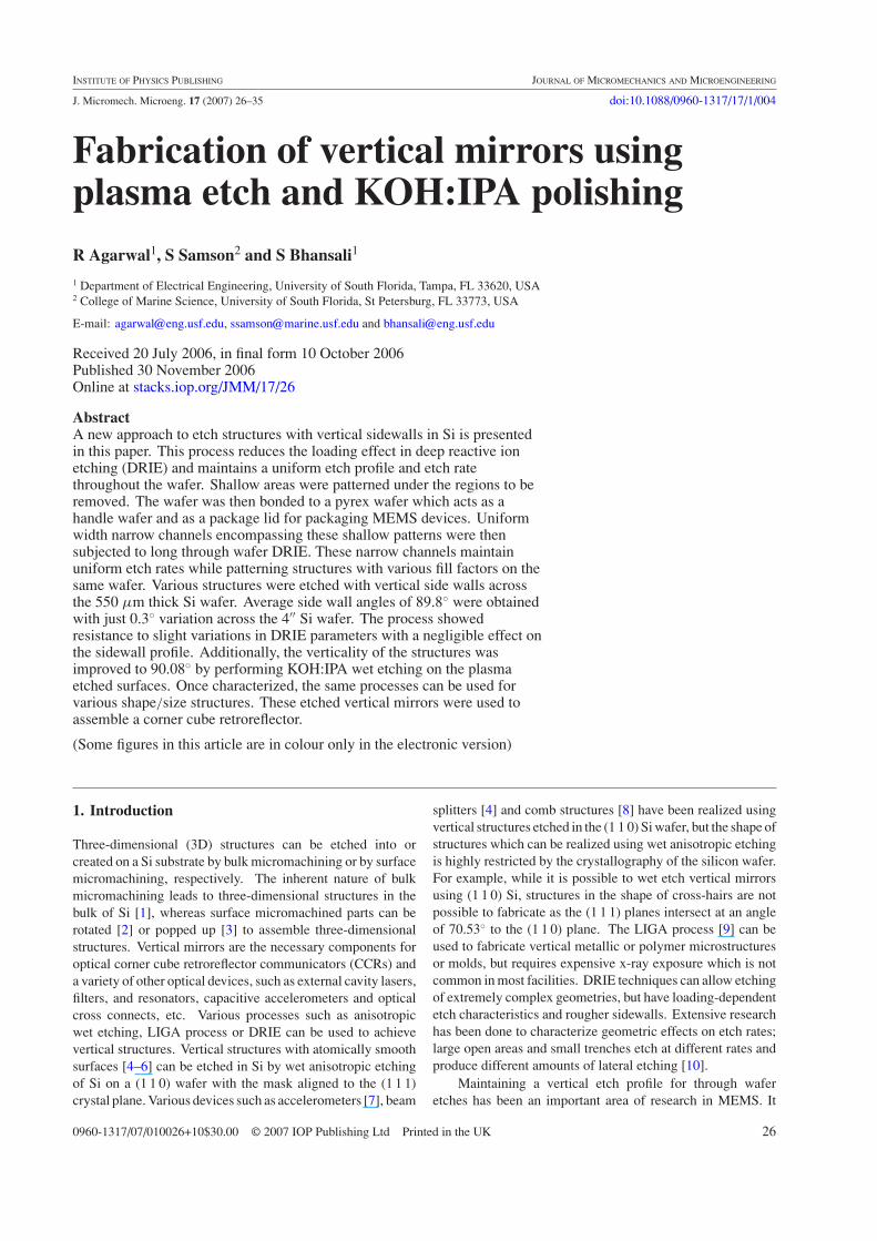
The various factors affecting the DRIE process in SF6 +C4F8 includes pressure, gas flow rates, RF power, distributionsof fluorine radicals, ions, waste products etc. In SF6 plasmaactive fluorine atoms are released from the plasma and reactwith the Si surface to form a volatile fluoride species. Thefluorine atoms reach the surface from all directions. But asthe etch depth increases, it limits the transport of fluorideatoms reaching the Si surface which results in reduction in etchrates and increased roughness. The geometry of the patternto be etched also has a major influence on the etch depth,profile and other process characteristics. These effects includeaspect-ratio dependent etching and the microloading effect
(a) (b)
Figure 1. DRIE etch profiles: (a) ideal; (b) typical.
where large open areas have a high reactant consumption rate.This leads to reactant deficits, since the transport of etchingspecies across the wafer is limited by the diffusion process asdescribed earlier. With the increase in density of open areas,the microloading effects increase resulting in decreased etchrates along with changes in etch profiles. Figure 1 shows twoDRIE etch profiles. Figure 1(a) shows the ideal DRIE profilewith vertical and smooth sidewalls, whereas figure 1(b) showsan exaggeration of the typical etch profile obtained in DRIEwith tapered sidewalls and a bowl shaped bottom [17]. Thesidewalls are rough because of the scalloping effect, and thebottom of the etch pit is bowl shaped due to the cyclic natureof the dry etch process. The angle θ is usually less than 90◦
and is approximately equal to tan−1 [2h/(Wp − Wm)], whereWp is the pattern width, Wm is the mask width and h is the etchdepth.
One way to reduce the microloading effect is to reducethe density of the open areas in DRIE. This was done by usinguniform narrow width channels all across the wafer. Uniformwidth was used to ensure that there was no DRIE lag betweendifferent structures.
The DRIE process leaves scallops on the morphologyof the etched structures because of the process sequenceof etch and passivation cycles, as shown in figure 1(b).To use these etched surfaces as mirrors the roughness hasto be reduced. There are various methods [5, 18–23] topolish the rough DRIE surface including oxidation and etchback, EPW (ethylenediamine, pyrocatechol and water), HNA(hydrofluoric acid, nitric acid and acetic acid) electropolishing,KOH:IPA etching, etc. Some of them are very hazardoussolutions and others have the potential to damage theco-bonded pyrex surface which is used in this work as thehandle wafer and the package lid. Helin et al [20] usedKOH etching on deep RIE structures to get the mirror surfacessmooth, and they used the crystallographic properties to getthe self alignment to fabricate rhombus shaped channels forthe fiber supports in the 〈1 1 0〉 direction.
Standard KOH solution in H2O has etch rates for differentcrystal planes in the order of (1 1 0) > (1 0 0) > (1 1 1).However, with the addition of IPA in the solution the etchrates in the (1 1 0) plane is decreased by about 90% while onlyreducing it by 20% in the (1 0 0) plane; hence the etch rateof different crystal planes in KOH:IPA solution is (1 0 0) >
(1 1 0) > (1 1 1) [5, 21–23].We used DRIE and wet anisotropic etching techniques
to first etch 550 µm deep structures in Si while maintaininga uniform etch profile, and then wet anisotropic etching toimprove the verticality of the etched structures and reducethe roughness, along with an in situ developed package
27
R Agarwal et al
(a)
(b)
(c)
(d)
(g)
( f )
(e) (h)
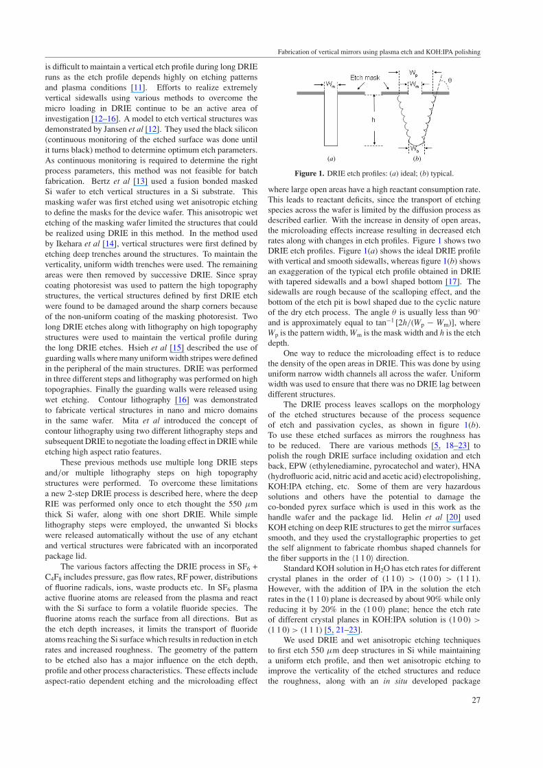
Figure 2. Cross-sectional view of the DRIE etch process to fabricate vertical mirrors: (a) LPCVD Si3N4 coated Si; (b) RIE of Si3N4
followed by 10 µm deep DRIE of Si; (c) photoresist was stripped off and anodic bonding was performed on the front side; (d) Si3N4 waspatterned to define the wet polishing mask; (e) sputtering of Al on the back side of Si; (f ) lithography was performed to define DRIEchannels with Al as DRIE masking layer, which overlaps the underlying Si3N4; (g) after completion of DRIE the unbonded structures arefreed from the bonded structures (h) highly vertical mirrors and package frame were left after removing the bulk Si.
window. Extremely vertical and deep structures with variousfill factors and a uniform etch rate and etch profile wereetched across the Si wafer. The front side of a Si waferwas shallow etched using DRIE to define eventual opticalwindows. This surface was then anodically bonded to a pyrexwafer. The exposed back side of the Si was then patternedto define narrow uniform width channels around each opticalwindow. These channels (50 µm) were vertically etched usingthough wafer DRIE, after which the unattached portions of thewindow region were removed. In the described work, longvertical mirrors were created using a single step DRIE method.These mirrors were then anisotropically polished in KOH:IPAsolution to reduce the surface roughness and were Au coatedto increase the reflectivity. A scheme for creating metal-coated vertical surfaces in silicon, along with an integratedtransparent package lid for assembling, packaging and testingMEMS devices has been presented before [24]. These bondedSi vertical mirrors and the glass window form the package liddevices which were then subsequently bonded to active torsionmirrors to fabricate a 3D MOEMS device called corner cuberetroreflector (CCR) as presented elsewhere [25].
2. Fabrication
To avoid the aforementioned loading effects in the DRIEprocess, which limits etch uniformity and can result in non-vertical structures, a 2-step DRIE process with uniform narrowwidth etch channels was devised, as illustrated in figure 2.The process consists of an initial deposition of a thin layer of100 nm LPCVD silicon nitride on a 4′′ double side polished(DSP) (1 0 0) Si wafer (840 ◦C, 200 mTorr.) in a Tystar LPCVDfurnace (mini Tytan 4600), as shown in figure 2(a). Thiswas followed by an indentation patterning on the front sideof the wafer to define eventual open areas of the packagewindow, with the mask rectangles aligned to the wafer flat〈1 1 0〉 direction. The nitride film was etched using reactive
ion etching (RIE) using a CHF3 and O2 plasma, followed bya very short silicon DRIE, using photoresist as the mask asshown in figure 2(b). This creates a few microns indentationinto the surface of the wafer. Next the resist was stripped offthe wafer and then this indented side (front side of Si wafer)was anodically bonded in a vacuum to a DSP pyrex 7740 glasswafer (EVG 501 bonder, 1 kV, 400 ◦C, 10 min), creating a bondeverywhere except where the indentation exists, as shown infigure 2(c). The nitride layer was sandwiched between thepyrex and Si. It prevents the formation of etch pit holes inSi, which was noticed during the wet etching tests (which willbe described later). The bonding strength was tested usingshear tester and it passed the load of 2 kg. The Si3N4 on thebackside of the Si wafer was then patterned with the KOH:IPAmask (the masks designs are shown in figure 3) as shown infigure 2(d). The stack of the wafer was coated with a 1000 Athick Al layer through sputtering as shown in figure 2(e). TheAl acts as a high etch selectivity etch mask for DRIE, while theunderlying Si3N4 was used as the wet etching mask in furtherprocessing. The Al was then patterned with a DRIE maskwhich overlaps the KOH:IPA mask by 10 µm. This definesthe narrow uniform width (50 µm wide) channels around allfixed features. The Al layer was etched in an Al etchant (TypeA, Transene Inc.) at 50 ◦C for 22 sec and is as shown infigure 2(f ). Thus, two different masking layers were createdfor DRIE and subsequent KOH:IPA polishing. These narrowuniform width channels were etched through the Si waferusing DRIE. Once the uniform width channel etch reaches theindentation areas, the large indented area of the Si detachesfrom the bonded Si and falls onto the pyrex surface, as shownin figure 2(g). After etching these pieces were removed just byinverting the wafer stack. The remaining parts still bonded tothe glass wafer are the vertical mirrors and the package frame,as in figure 2(h). Al was stripped off using Al etchant and wetanisotropic polishing was performed to improve the surfacequality, as discussed in section 4.
28
Fabrication of vertical mirrors using plasma etch and KOH:IPA polishing
(a) (b)
(d)
(c)
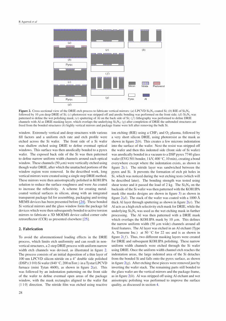
Figure 3. Mask layout used to fabricate vertical mirrors in the shape of a cross-hair. (a) The indentation mask where only the masked areawas shallow etched in DRIE. (b) The KOH:IPA etch mask. This mask was used to pattern Si3N4 before using the DRIE mask to makedifferent masking layers for KOH:IPA polishing and DRIE. (c) DRIE mask with only narrow uniform width channels of 50 µm. It definesthe narrow channels where through wafer DRIE was performed. This mask overlaps the KOH:IPA polish mask by10 µm. (d) Shows all the three masks overlaying each other.
3. Experimentation
The average sidewall angle of the etched structures, measuredfrom the SEM images, using the above described method was89.8◦. Since DRIE was performed using uniform width etchchannels, very uniform etch features of different shapes andsizes were obtained across the wafer. Figure 3 shows the masklayout used to fabricate vertical structures for the CCR in across shape. The indentation mask (figure 3(a)) was patternedusing a negative photoresist so that the area which is shown inthe mask gets etched in the first DRIE step for 10–15 µm. TheKOH:IPA mask, shown in figure 3(b), was then used to patternthe Si3N4 layer on the back side of the wafer. Al was thensputtered on the back side and the DRIE mask (figure 3(c))was used to pattern this Al which will act as a DRIE maskinglayer. The indentation mask lies between the 50 µm wideDRIE mask features so that the misalignment which mightoccur in front and back side alignment does not affect theDRIE process which will release the unwanted areas from thewafer. The DRIE mask overlaps the KOH:IPA mask by 10 µm,which is more than the alignment tolerance of the mask aligner,and to account for the tool non-uniformity during long etches.The Si3N4 layer will be used later to improve the smoothnessand verticality of DRIE etched surfaces. Over etching forapproximately 50 cycles was done to make sure that all theunwanted blocks fell off on the pyrex. No effect of thisover etch was noticed on the roughness or verticality of thestructures. Figure 3(d) shows how the different masks overlapeach other. Various kinds of features were etched on thesame wafer with different fill factors. In all of them the
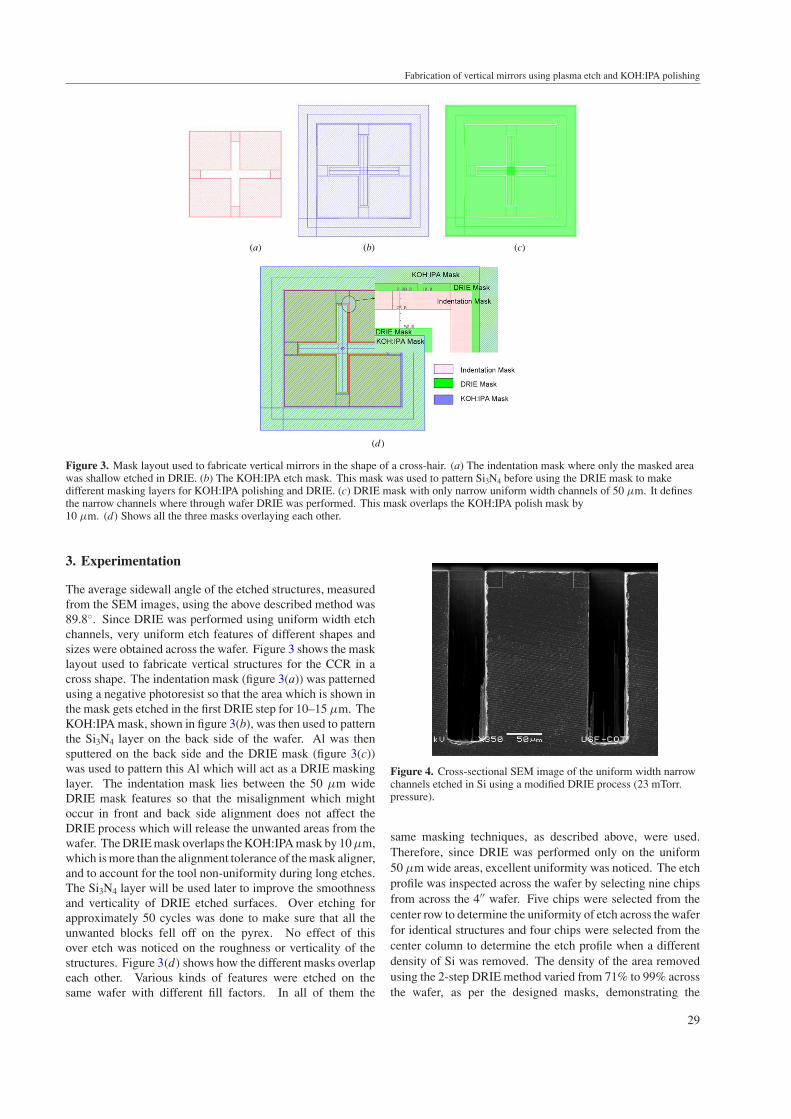
Figure 4. Cross-sectional SEM image of the uniform width narrowchannels etched in Si using a modified DRIE process (23 mTorr.pressure).
same masking techniques, as described above, were used.Therefore, since DRIE was performed only on the uniform50 µm wide areas, excellent uniformity was noticed. The etchprofile was inspected across the wafer by selecting nine chipsfrom across the 4′′ wafer. Five chips were selected from thecenter row to determine the uniformity of etch across the waferfor identical structures and four chips were selected from thecenter column to determine the etch profile when a differentdensity of Si was removed. The density of the area removedusing the 2-step DRIE method varied from 71% to 99% acrossthe wafer, as per the designed masks, demonstrating the
29
R Agarwal et al
Table 1. Showing the various parameters used in the standardBosch cycles.
Passivation cycle Etch A Etch B
Pressure (mTorr) 22 23 23Cycle time (sec) 5 2 6C4F8 (cc) 70 0.5 0.5SF6 (cc) 0.5 50 100Ar (cc) 40 40 40RIE power (RF1) (W) 1 9 9ICP power (RF2) (W) 825 825 825
Table 2. Comparison of sidewall angles across the wafer withdifferent DRIE recipes.
Sidewall angle Sidewall angle Sidewall angle(6 sec (5 sec (5 secpassivation, passivation, passivation,22 mtorr) 22 mtorr) 23 mtorr)
Sample in DRIE in DRIE in DRIE
Left 89.62◦ 90.04◦ 89.72◦
Left center 90.03◦ 90.17◦ 89.80◦
Center 90.01◦ 90.10◦ 89.91◦
Right center 89.84◦ 90.15◦ 89.91◦
Right 89.67◦ 90.08◦ 89.80◦
Top 89.45◦ 90.15◦ 90.05◦
Top center 89.85◦ 90.20◦ 89.82◦
Center 90.01◦ 90.10◦ 89.91◦
Bottom center 90.10◦ 90.09◦ 89.85◦
Bottom 89.90◦ 90.65◦ 89.80◦
Average 89.85◦ 90.17◦ 89.86◦
removal of large areas, with minimal change in the sidewallprofile.
The DRIE was performed in a Unaxis SLR-7701-10R-BBosch DRIE system, and the passivation cycle and the etchcycles parameters are shown in table 1.
Figure 5. Scattering loss versus rms roughness at various incident angles for the He–Ne laser.
Pyrex Wafer
89.80
Al
Si3N4
Near (110) scalloped plane
Pyrex Wafer
90.080
Al
Si3N4
Polished (110)plane
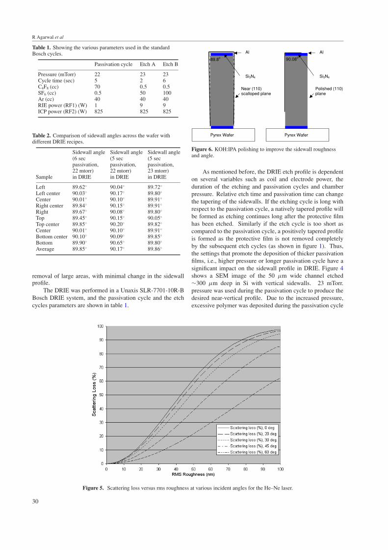
Figure 6. KOH:IPA polishing to improve the sidewall roughnessand angle.
As mentioned before, the DRIE etch profile is dependenton several variables such as coil and electrode power, theduration of the etching and passivation cycles and chamberpressure. Relative etch time and passivation time can changethe tapering of the sidewalls. If the etching cycle is long withrespect to the passivation cycle, a natively tapered profile willbe formed as etching continues long after the protective filmhas been etched. Similarly if the etch cycle is too short ascompared to the passivation cycle, a positively tapered profileis formed as the protective film is not removed completelyby the subsequent etch cycles (as shown in figure 1). Thus,the settings that promote the deposition of thicker passivationfilms, i.e., higher pressure or longer passivation cycle have asignificant impact on the sidewall profile in DRIE. Figure 4shows a SEM image of the 50 µm wide channel etched∼300 µm deep in Si with vertical sidewalls. 23 mTorr.pressure was used during the passivation cycle to produce thedesired near-vertical profile. Due to the increased pressure,excessive polymer was deposited during the passivation cycle
30
Fabrication of vertical mirrors using plasma etch and KOH:IPA polishing
(b)
(c)
(a)
Figure 7. Optical profilometer scan of the vertical mirrors: (a) scan after DRIE, Ra = 149.85 nm; (b) after O2 plasma in DRIE,Ra = 90.09 nm; (c) after O2 plasma and anisotropic etching in KOH:IPA solution for 1 h Ra = 38.97 nm.
which was not being removed during the successive etchcycle. This results in the formation of micro-grass, as canbe seen in figure 4. This micro-grass was easily removed byKOH:IPA polishing.
In our experiments the pressure and time were changedin the passivation cycle to monitor their effect on the sidewallprofile using the above-described 2-step DRIE method. Thepassivation cycle duration was increased by 1 sec in the DRIEprocess or the C4F8 gas pressure was changed from 22 mTorr.to 23 mTorr. and the changes in sidewall angles were noted.The sidewall angles obtained from all of these samples were±0.2◦ of 90◦ indicating that the described process maintains itsvertical profile even with slight variations in the DRIE process
parameters. The sidewall angle variations on these samplesare summarized in table 2. The averaged variation acrossthe wafers was 0.3◦, with a ±1.5% measurement uncertainty.(1 0 0) Si wafers and (1 1 0) Si wafers were etched using theabove-described 2-step DRIE process without any significantvariation in sidewall angles.
Due to the etch rate variation across the wafer in DRIE,an over etch of ∼50 cycles in the second DRIE step wasperformed to make sure that all the chips across the wafer wereetched through and the unwanted blocks fell off, as shown infigure 2(g). The side wall profile was measured using theSEM images and the data are shown in table 2. Samples werepicked from across the wafer and the side wall angle variation
31
R Agarwal et al
(a) (b)
Figure 8. SEM image of the vertical structures (a) etched in a cross shape, polished and metallized; (b) smaller crosshair without anymetallization.
89.91
90.290.08
90.2190.07 90.02
89
89.2
89.489.6
89.8
90
90.2
90.490.6
90.8
91
1 2 3 4 5 6Sample number
Sid
e-W
all
An
gle
Figure 9. Sidewall angles after 2-step DRIE and 1 h KOH:IPApolishing.
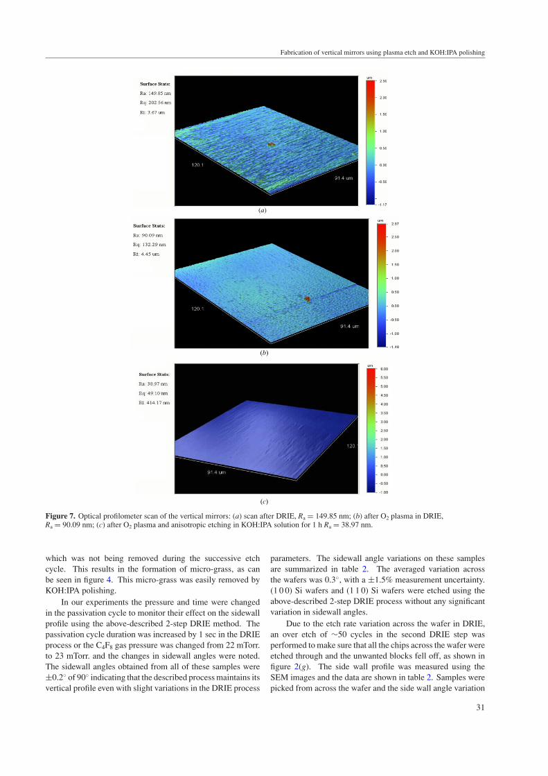
was 0.3◦ across the wafer with an average angle of 89.8◦.This variation can be attributed to the over etching or toolnon-uniformity. The average sidewall roughness after DRIEwas measured to be ∼150 nm using an optical profilometer.The average roughness after the polishing was measured tobe ∼40 nm and the average side wall angle was improvedto 90.08◦.
4. Wet anisotropic etching on vertical structures
Test chips were diced, so that the etched sidewall wasvisible when the chip was placed on its edge, to allow themeasurement of the roughness of the etched surfaces. Theaverage sidewall roughness obtained on the vertical structureetched using DRIE was measured to be 150 nm using an opticalprofilometer.
It has been shown that as long as the rms roughness ofthe mirror stays below 5% of the wavelength of the incidentlight, the reflected light flux is proportional to the incidentpower spectral density [21]. For a gently sloped surface, theamount of scattered light may be calculated from the rmssurface roughness σ using the relationship
PScat
Ptot= 1 − e−( 4πσ cos θ
λ)2
where Pscat is the scattered light flux and Ptot is the totalreflected light flux, λ is the wavelength of the incident light
beam and θ is the angle of incidence. Figure 5 shows thechange in scattering loss versus rms roughness at variousincident angles for a He–Ne laser (λ = 632.8 nm).
The average roughness on the DRIE sidewalls wasmeasured to be ∼150 nm. For visible optical applicationsthe 150 nm rms roughness is unacceptable, as 98% of theincident light (at an angle of 45◦) would be lost in scattering.Also, a teflon-like polymer (polymerized CF2) layer of∼50 nm gets deposited on all the exposed surfaces includingthe etched mirrors which prohibits post DRIE chemical etchingon this surface. This polymer was plasma cleaned in a Teplaplasma etcher, at RF power of 400 W and 400 sccm of O2 flowfor 1 h. This decreased the roughness of the etched surfacefrom 150 nm to 90 nm. The roughness of the vertical mirrorswas further reduced using anisotropic etching in KOH:IPAsolution with nitride as the masking layer.
The Si3N4 layer was protected while doing anodicbonding, as shown in figure 2(d). This was done to preventdamage and etch pit formation at the Si–pyrex interface,which was noticed during KOH:IPA polishing tests. Thusthis LPCVD Si3N4 on the front side of Si acts as the maskinglayer for the bonded interface.
To allow for some DRIE undercutting and slightmisalignment during photolithography two step masks wereused before DRIE was performed on the structures. Figure 6shows a schematic of the cross section of the structures afterDRIE and before and after the polishing step. The LPCVDnitride on the back side was patterned first so that the width ofthe nitride mask is narrower than the following Al mask. Thepolishing was performed at 50 ◦C for 1 h in 3M:2M::KOH:IPAsolution.
As mentioned before, the lithography was performed sothat the masks were aligned to the 〈1 1 0〉 direction of thecrystal planes. Therefore, after DRIE the vertical structuresare very near the (1 1 0) plane. When the vertical structureswith sidewalls near (1 1 0) planes were etched in a KOH:IPAsolution, slow etching (1 1 0) planes gets exposed and acts asthe etch stop plane which reduces the sidewall roughness to39 nm. Figure 7 shows the optical scans of the etched surfacesat the different stages of fabrication.
32
Fabrication of vertical mirrors using plasma etch and KOH:IPA polishing
(a) (b)
Figure 10. (a) Surface micromachined MEMS chip with a bond frame for vertical mirrors and active torsion mirrors; (b) assembled cornercube retroreflector.
(a) (b)
(c) (d )
Figure 11. SEM images of various vertical structures etched on the same wafer along with the crosshairs shown in figure 9.
5. Results and discussion
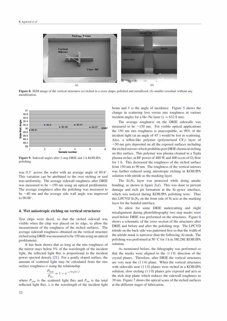
Figure 8 shows SEM images of cross-hair structures, whichwere etched in Si using the described 2-step DRIE process.Figure 8(a) shows the zoomed out image of a smallercross-hair, which shows the vertical structures along withthe package frame and package window (glass lid), beforepolishing. Figure 8(b) shows the magnified image of a similarcross-hair, showing the verticality and surface quality of thestructures after DRIE and KOH:IPA polishing.
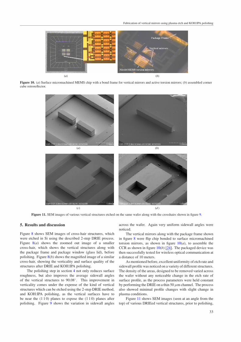
The polishing step in section 4 not only reduces surfaceroughness, but also improves the average sidewall anglesof the vertical structures to 90.08◦. This improvement inverticality comes under the expense of the kind of verticalstructures which can be etched using the 2-step DRIE method,and KOH:IPA polishing, as the vertical surfaces have tobe near the (1 1 0) planes to expose the (1 1 0) planes afterpolishing. Figure 9 shows the variation in sidewall angles
across the wafer. Again very uniform sidewall angles werenoticed.
The vertical mirrors along with the package frame shownin figure 8 were flip chip bonded to surface micromachinedtorsion mirrors, as shown in figure 10(a), to assemble theCCR as shown in figure 10(b) [24]. The packaged device wasthen successfully tested for wireless optical communication ata distance of 10 meters.
As mentioned before, excellent uniformity of etch rate andsidewall profile was noticed on a variety of different structures.The density of the areas, designed to be removed varied acrossthe wafer without any noticeable change in the etch rate ofsurface profile, as the process parameters were held constantby performing the DRIE on a thin 50 µm channel. The processalso showed minimal profile changes with slight change inplasma conditions.
Figure 11 shows SEM images (seen at an angle from thetop) of various DRIEed vertical structures, prior to polishing,
33
R Agarwal et al
with different fill factors, which were etched on the samewafer using the 2-step DRIE process. The added advantage ofthis process is the in-situ fabrication of the package lid framewhich can be used in various applications. Figures 11(a) and(b) show the vertical structures etched on a (1 1 0) Si waferwith the structures aligned to the (1 1 1) planes. Such devicescan be KOH-polished and bonded sequentially to the thirdwafer, for example the torsion mirrors chip, which is shown infigure 10(a), to assemble a CCR. A packaged accelerometercan be fabricated easily using the described process wherethe proof mass is etched in Si, as shown in figure 11(c) orfigure 11(d).
Etch rates of approximately 2.6 µm min−1 were recordedusing this 2-step DRIE method. There is a trade off betweenetch rates and verticality, depending on the width of the pattern.Increase in the width will result in fast etches but the verticalitymight be compromised. Decrease in the width might resultin better verticality but the etch rates will decrease. 50 µmwidth was chosen by the authors, but optimization may needto be done to find a sweet spot between these two parameters.However, the optimization would not be needed for differentstructures but only for a desired channel width.
A drawback of this method is that two lithography maskswere used instead of a single mask as in the conventional DRIEprocess. This increases the design and lithography cost but,nevertheless, the cost reduction in process gas consumption,and etch uniformity is more lucrative than the lithographycost. Newer ICP etch equipments claim to achieve a 90◦
sidewall profile [26] with an etch rate of 10 µm min−1.However, optimization of the etch recipe is required fordifferent structures. Moreover, the sidewall roughnessobtained by these tools is not suitable for optical applications.These tools might not be of interest for the researchers whoalready have a DRIE tool. The described process demonstratesa process which should work on most of the DRIE toolswith any kind of etch pattern and density. No optimizationis required for different shaped structures.
6. Conclusions
Methods to produce deep vertical mirrors, on a 550 µm thickSi wafer, which was anodically bonded to a pyrex wafer ispresented. The pyrex wafer acts as the handle wafer duringDRIE and also forms the package window while encapsulatingthe final device. The roughness of the DRIE surfaces wasreduced using KOH:IPA polishing and the verticality wasimproved from 89.8◦ to 90.08◦. Highly uniform etch rateswere obtained across the wafer. 0.3◦ sidewall angle variationwas recorded across the wafer, while various kinds of verticalstructures, with different fill factors were etched using thesame processes on the same wafer. With this method nore-characterization of the tool is needed for different structureswith various shapes and fill factors. The loading effect wasminimized by using a uniform width narrow channel openingacross the wafer for DRIE. A packaged device corner cuberetroreflector (CCR) is shown using the DRIE etched andKOH:IPA polished vertical mirrors which were bonded to theMEMS torsion mirrors.
Acknowledgments
The authors would like to acknowledge the US Army,Space and Missile Defense Command for support of thiswork through contract #DASG60-00-C-0089. Distribution A.approved for publish release: distribution unlimited.
References
[1] Peterson K E 1982 Silicon as a mechanical material Proc.IEEE 70 420–57
[2] Pister K S J, Judy M W, Burgett S R and Fearing R S 1992Microfabricated hinges Sensors Actuators A 33 249–56
[3] King C R, Lin L Y and Wu M C 1996 Monolithicallyintegrated refractive microlens standing perpendicular to thesubstrate Proc. SPIE Photonics West’96 vol 2687 pp 123–30
[4] Uenishi Y, Tsugai M and Mehregany M 1995Micro-opto-mechanical devices fabricated by anisotropicetching of (1 1 0) silicon J. Micromech. Microeng. 5 305–12
[5] Zubel I and Kramkowska M 2001 The effect of isopropylalcohol on etching rate and roughness of (1 0 0) Si surfaceetched in KOH and TMAH solutions Sensors ActuatorsA 93 138–47
[6] Krause P and Obermeier E 1995 Etch rate and surfaceroughness of deep narrow U-grooves in (1 1 0)-orientedsilicon J. Micromech. Microeng. 5 112–4
[7] Ciarlo D R 1992 A latching accelerometer fabricated by theanisotropic etching of (1 1 0) oriented silicon wafersJ. Micromech. Microeng. 2 10–3
[8] Kim S H, Lee S H, Lim H T and Kim Y K 1997 (1 1 0) siliconetching for high aspect ratio comb structures IEEE Proc.Emerging Technologies and Factory Automation pp 248–52
[9] Guckel H 1998 High-aspect-ratio micromachining via deepx-ray lithography Proc. IEEE 86 1586–93
[10] Jensen S and Hansen O 2004 Characterization of themicroloading effect in deep reactive ion etching of siliconProc. SPIE Micromach. Microfab. 5342 111–8
[11] Jansen H, Gardeniers B M, Elwenspoek M and Fluitman J1996 A survey on the reactive ion etching of silicon inmicrotechnology J. Micromech. Microeng. 6 14–28
[12] Jansen H, Boer M, Legtenberg R and Elwenspoek M 1995 Theblack silicon method: a universal method for determiningthe parameter setting of a fluorine-based reactive ion etcherin deep silicon trench etching with profile controlJ. Micromech. Microeng. 5 115–20
[13] Bertz A and Warner T 1994 The formation of very flat siliconsidewalls by dry etching J. Micromech. Microeng. 4 23–7
[14] Ikehara T and Maeda R 2005 Fabrication of an accuratelyvertical sidewall for optical switch applications using deepRIE and photoresist spray coating J. Microsyst. Technol.12 98–103
[15] Hsieh J and Fang W 2002 A boron etch-stop assisted lateralsilicon etching process for improved high-aspect-ratiosilicon micromachining and its applications J. Micromech.Microeng. 12 574–81
[16] Mita Y, Kubota M, Harada T, Marty F, Saadany B,Bourouina T and Shibata T 2006 Contour lithographymethods for DRIE fabrication of nanometer–millimetre-scale coexisting Microsystems J. Micromech. Microeng.16 S135–41
[17] Ayon A A, Zhang X and Khanna R 2001 Anisotropic silicontrenches 300–500 mm deep employing time multiplexeddeep etching (TMDE) Sensors Actuators A 91 381–85
[18] Sasaki M, Fujii T, Li Y and Hane K 2001 Anisotropic Sietching technique for optically smooth surfacesTransducers’01 pp 604–7
[19] Mihalcea C, Khumpuang S and Kuwahara M 2001 Ultra-fastanisotropic silicon etching with resulting mirror surfaces inammonia solutions Transducers’01 pp 608–11
34

Fabrication of vertical mirrors using plasma etch and KOH:IPA polishing
[20] Helin P, Mita M, Bourouina T, Reyne G and Fujita H 2000Self-aligned micromachining process for large-scale,free-space optical cross-connects J. Lightwave Technol.18 1785–91
[21] Marxer C, Gretillat M-A, De Rooij N F, Battig R,Anthamatten O, Valk B and Vogel P 1997 Vertical mirrorsfabricated by reactive ion etching for fiber optical switchingapplications Proc. IEEE 10th Annual Int. Workshoppp 49–54
[22] Lv Y, Ma J, Zou J and Wang X 2002 Research ofanisotropic etching in KOH water solution withisopropyl alcohol International Conference onCommunication, Circuits and Systems vol 2pp 1779–83
[23] Nilsson D, Jensen S and Menon A 2003 Fabrication of siliconmolds for polymer optics J. Micromech. Microeng.13 S57–S61
[24] Agarwal R, Samson S, Kedia S and Bhansali S 2006Fabrication of integrated vertical mirror surfaces andtransparent window for packaging MEMS devicesJMEMS at press
[25] Samson S, Agarwal R, Kedia S, Wang W, Onishi S andBumgarner J 2005 Fabrication processes for packagedoptical MEMS devices Proc. ICMENS (Canada) pp 113–8
[26] Pandhumsoporn T, Wang L, Feldbaum M and Gadgil P 1998High-etch-rate deep anisotropic plasma etching of siliconfor MEMS fabrication Proc. SPIE on Smart Structures andMaterials vol 3328 pp 93–101
35


![Coronal Polishing Revised.doc - [CSI] College of Southern Idaho](https://img.dokumen.tips/doc/110x75/631c5d9676d2a4450503822b/coronal-polishing-reviseddoc-csi-college-of-southern-idaho.jpg)


