Embed Size (px)
Citation preview

Fabrication of gold nanostructures through pulsed laser interference patterningDajun Yuan, Ranadip Acharya, and Suman Das
Citation: Applied Physics Letters 103, 223101 (2013); doi: 10.1063/1.4833548 View online: http://dx.doi.org/10.1063/1.4833548 View Table of Contents: http://scitation.aip.org/content/aip/journal/apl/103/22?ver=pdfcov Published by the AIP Publishing Articles you may be interested in Laser nanostructuring of polymers: Ripples and applications AIP Conf. Proc. 1464, 372 (2012); 10.1063/1.4739891 GaAs nanostructuring by self-organized stencil mask ion lithography J. Appl. Phys. 110, 114321 (2011); 10.1063/1.3665693 Technology platform for the fabrication of titanium nanostructures J. Vac. Sci. Technol. B 29, 06FG06 (2011); 10.1116/1.3657517 Angular effects of nanostructure-covered femtosecond laser induced periodic surface structures on metals J. Appl. Phys. 108, 073523 (2010); 10.1063/1.3487934 Patterning of nanostructured thin films by structured light illumination Appl. Phys. Lett. 87, 143103 (2005); 10.1063/1.2061857
This article is copyrighted as indicated in the article. Reuse of AIP content is subject to the terms at: http://scitation.aip.org/termsconditions. Downloaded to IP:
130.207.50.37 On: Mon, 25 Aug 2014 16:30:02
Fabrication of gold nanostructures through pulsed laser interferencepatterning
Dajun Yuan,1,a),b) Ranadip Acharya,1,b),c) and Suman Das1,2,d)
1Woodruff School of Mechanical Engineering, Georgia Institute of Technology, Atlanta, Georgia 30332, USA2School of Materials Science & Engineering, Georgia Institute of Technology, Atlanta, Georgia 30332, USA
(Received 5 July 2013; accepted 10 November 2013; published online 25 November 2013)
In this Letter, we report on the experimental development and computational modeling of a simple,
one-step method for the fabrication of diverse 2D and 3D periodic nanostructures derived from
gold films on silicon substrates and over areas spanning 1 cm2. These nanostructures can be
patterned on films of thickness ranging from 50 nm to 500 nm with pulsed interfering laser beams.
A finite volume-based inhomogeneous multiphase model of the process shows reasonable
agreement with the experimentally obtained topographies and provides insights on the flow physics
including normal and radial expansion that results in peeling of film from the substrate. VC 2013AIP Publishing LLC. [http://dx.doi.org/10.1063/1.4833548]
Gold nanostructures have been extensively studied.1
Several important discoveries have been revealed recently,
such as large enhancement of nonlinear optical phenomena,2
surface-enhanced Raman scattering,3 and cell probe.4 A
number of approaches such as E-beam lithography,5 laser
direct-writing,6 nanosphere lithography,7 and nanoimprint
lithography8 have demonstrated successful fabrication of
gold nanostructures. However, they are constrained either by
high cost, low throughput, or limited ability to produce high
aspect ratio nanostructures over large areas relative to nano-
structure dimensions (>1 cm2). Laser interference patterning
(LIP) makes use of the interference of two or more
high-power pulsed laser beams, and involves just a
single-step process. This technique allows the production of
periodic structures with a well-defined long-range order in
length scales ranging from a quarter of the wavelength to
tens of micrometers, simply through the adjustment of the
angles between interfering beams. The structuring process is
based on photo-thermal, photo-physical, or photo-chemical
mechanisms, depending on the type of the material.
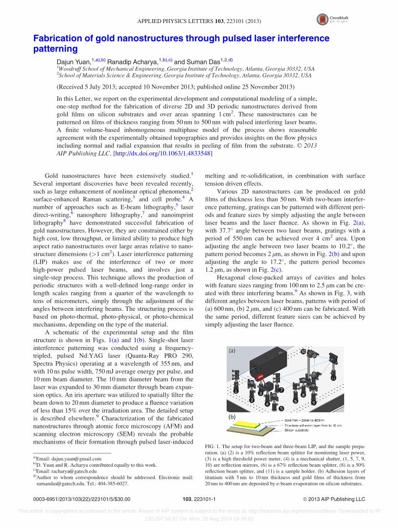
A schematic of the experimental setup and the film
structure is shown in Figs. 1(a) and 1(b). Single-shot laser
interference patterning was conducted using a frequency-
tripled, pulsed Nd:YAG laser (Quanta-Ray PRO 290,
Spectra Physics) operating at a wavelength of 355 nm, and
with 10 ns pulse width, 750 mJ average energy per pulse, and
10 mm beam diameter. The 10 mm diameter beam from the
laser was expanded to 30 mm diameter through beam expan-
sion optics. An iris aperture was utilized to spatially filter the
beam down to 20 mm diameter to produce a fluence variation
of less than 15% over the irradiation area. The detailed setup
is described elsewhere.9 Characterization of the fabricated
nanostructures through atomic force microscopy (AFM) and
scanning electron microscopy (SEM) reveals the probable
mechanisms of their formation through pulsed laser-induced
melting and re-solidification, in combination with surface
tension driven effects.
Various 2D nanostructures can be produced on gold
films of thickness less than 50 nm. With two-beam interfer-
ence patterning, gratings can be patterned with different peri-
ods and feature sizes by simply adjusting the angle between
laser beams and the laser fluence. As shown in Fig. 2(a),
with 37.7� angle between two laser beams, gratings with a
period of 550 nm can be achieved over 4 cm2 area. Upon
adjusting the angle between two laser beams to 10.2�, the
pattern period becomes 2 lm, as shown in Fig. 2(b) and upon
adjusting the angle to 17.2�, the pattern period becomes
1.2 lm, as shown in Fig. 2(c).
Hexagonal close-packed arrays of cavities and holes
with feature sizes ranging from 100 nm to 2.5 lm can be cre-
ated with three interfering beams.9 As shown in Fig. 3, with
different angles between laser beams, patterns with period of
(a) 600 nm, (b) 2 lm, and (c) 400 nm can be fabricated. With
the same period, different feature sizes can be achieved by
simply adjusting the laser fluence.
FIG. 1. The setup for two-beam and three-beam LIP, and the sample prepa-
ration. (a) (2) is a 10% reflection beam splitter for monitoring laser power,
(3) is a high threshold power meter, (4) is a mechanical shutter, (1, 5, 7, 9,
10) are reflection mirrors, (6) is a 67% reflection beam splitter, (8) is a 50%
reflection beam splitter, and (11) is a sample holder. (b) Adhesion layers of
titanium with 5 nm to 10 nm thickness and gold films of thickness from
20 nm to 400 nm are deposited by e-beam evaporation on silicon substrates.
a)Email: [email protected])D. Yuan and R. Acharya contributed equally to this work.c)Email: [email protected])Author to whom correspondence should be addressed. Electronic mail:
[email protected]. Tel.: 404-385-6027.
0003-6951/2013/103(22)/223101/5/$30.00 VC 2013 AIP Publishing LLC103, 223101-1
APPLIED PHYSICS LETTERS 103, 223101 (2013)
This article is copyrighted as indicated in the article. Reuse of AIP content is subject to the terms at: http://scitation.aip.org/termsconditions. Downloaded to IP:
130.207.50.37 On: Mon, 25 Aug 2014 16:30:02

As the thickness of gold film increases to more than
200 nm, different kinds of 3D structures can be fabricated
over large area. The laser fluence is calculated as follows:
laser fluence (J/cm2)¼ average laser power (w) x exposure
time (s)/the exposure area (cm2). With relatively low laser
fluence, 300 mJ/cm2, micro-dome shape structures can be
formed, as shown in Fig. 4(a). When the laser fluence is
increased to 500 mJ/cm2, micro-mushroom shape structures
can be formed, as shown in Fig. 4(b). The total height of the
structure is around 1.6 lm, the diameter of the ball on the top
is around 500 nm, and the diameter of the neck connecting
the ball to the base is around 200 nm. Millions of
micro-mushroom structures can be formed over 1 cm2 area
with 2.5 lm periodic spacing. When the laser fluence is
increased to 700 mJ/cm2, the stem is pinched off in the
molten state and the sub-micrometer size balls detach from
the base, resulting in sharp needle-shaped structures, as
shown in Fig. 4(c). The diameter of the bottoms of the tips is
around 100 nm, at the tops of the tips is around 10 nm, and
the needle height is around 400 nm. An intermediate stage is
formed with laser fluence of 605 mJ/cm2. Due to slight local
variations in the fluence, some of the sub-micrometer balls
are detached due to stem pinch-off while some of them are
still connected to the stem and base, as shown in Fig. 4(d).
The flow physics of such structure formation processes
has evoked a lot of interest lately. Since noble metals exist
much longer in the molten state, Marangoni convection plays
an important role10 in the associated flow due to laser melt-
ing. The surface tension coefficient decreases with increasing
temperature. The higher surface tension present in colder
regions exerts a pull on the liquid in hotter regions.
Therefore, liquid convection will take place from regions of
higher temperature to regions of lower temperature. The
pressure of evaporation of the solute film is thought to play a
dominant role in the peeling of the film and the formation of
the shell-like structure.11 A model of elasto-plastic flow
combined with the two-temperature model (TTM) in a two-
dimensional approximation has been developed to describe
microbump and nanojet formation.12 Recently, a molecular
dynamics (MD) simulation coupled with TTM model has
been applied to Ni films.13 The MD-TTM simulation result
indicates that nano-bump formation is a four-stage process
comprising of compressive stress generation, peeling of film,
normal and radial expansion. However, the effect of plastic
deformation and pressure of the vaporized film was not
observed in the MD simulation. Nevertheless, the TTM-MD
simulation still required 128 processors and about 1000 h of
calculation for a 250 ps long simulation.13
FIG. 2. 2D gold nanostructures with periods of (a) 550 nm (b) 2 lm, and
(c) 1.2 lm fabricated with two-beam LIP.
FIG. 3. 2D gold nanostructures with periods of (a) 600 nm (b) 2 lm, and
(c) 400 nm fabricated with three-beam LIP.
FIG. 4. 3D gold nanostructures with periods of 2.5 lm fabricated with
three-beam LIP (a) for laser power¼ 300 mJ/cm2, (b) for laser
power¼ 500 mJ/cm2, (c) for laser power¼ 700 mJ/cm2, and (d) for laser
power¼ 605 mJ/cm2.
223101-2 Yuan, Acharya, and Das Appl. Phys. Lett. 103, 223101 (2013)
This article is copyrighted as indicated in the article. Reuse of AIP content is subject to the terms at: http://scitation.aip.org/termsconditions. Downloaded to IP:
130.207.50.37 On: Mon, 25 Aug 2014 16:30:02

Nanostructure formation driven by the hydrodynamic
effect in laser irradiation processes has been simulated using
finite difference approaches in earlier works.14,15 However,
these approaches were limited to the consideration of hydro-
dynamic and surface tension forces only. In our work, a com-
plete inhomogeneous multiphase model is solved and the
effect of interfacial drag between air and the liquefied metal
is modeled. Furthermore, the effect of the substrate is incor-
porated using a conjugate heat transfer model. The Navier-
Stokes equation is employed with the surface tension force
modeled as volume force term concentrated at the interface16
to investigate the formation of nano-bumps on gold films
due to interaction with laser beam. The key physics that have
been modeled include: (a) phase change phenomenon
(melting and solidification), (b) interfacial drag force
between liquid gold and air, (c) surface tension between liq-
uid gold and air, (d) buoyancy (due to density differences
between the different phases), and (e) conjugate heat transfer
between the gold film and the Si Substrate. In the model, the
following assumptions were made: (1) superheating of the
liquid gold film is not implemented and is treated as if it is in
isothermal condition.14 (2) The liquid gold film is modeled
as dispersed phase with diameter of 10 nm. The air and solid
gold are modeled as continuous phases. (3) The flow is lami-
nar. (4) Thermal radiation is not included. (5) The thermal
interaction between the atmosphere and the gold film is not
included. (6) Property values are constant.15 The surface ten-
sion value is averaged over the temperature range.17
The computational fluid dynamics (CFD) model is
solved in ANSYS CFX to predict the topography of the
nanostructure formed. For the 0.2 lm film, a domain size of
11 lm is chosen in the z-direction to ensure little/no bound-
ary interaction. This domain extent size is sufficient to
accommodate the nano-structure formed. A 1 lm thick Si
substrate is modeled in the z-direction. Due to symmetry,
2.5 lm of the film region in the x and y directions is mod-
eled, which corresponds to one wavelength of the laser inten-
sity profile. The entire simulation is solved in an Intel Xeon
workstation and took 85 h of calculation to solve for 20 ns
long simulation while running on 2 processors.
The continuity equation18 for each phase is solved. The
momentum equation is solved for each phase a. The interfa-
cial drag between air and liquid gold is modeled using parti-
cle model and the drag coefficient is obtained using the
Schiller-Naumann19 model. The drag force between air and
solid gold is modeled using mixture model and a drag coeffi-
cient of 0.01 is assumed. However, one solidification sink in
the momentum model is used to keep the solid gold velocity
at a zero value.
For each phase present, the thermal energy equation
is solved.18 The two-resistance model is used at the solid
gold-liquid gold interface to model the interphase mass
transfer. For the liquid side, infinite fluid specific heat trans-
fer coefficient or zero resistance is used while for the solid
side, the Ranz-Marshall20 correlation is used. Fig. 5 shows
the mesh of the multi-domain model with boundary condi-
tions imposed on them. Here, the gravity vector is oriented
in the negative z-direction.
The entire set of equations along with the necessary
boundary conditions is solved in ANSYS CFX, a finite element-
based finite volume CFD software. The solidification sink
and the transient source term are implemented through CFX
Expression Language (CEL). The flow in each case is simu-
lated for 20 ns with a time step of 10�11 s, while the source
is operational for 10 ns.
The CFD result matches reasonably well with the MD
simulation results. In Fig. 6, red color indicates higher value
of gold mass fraction and blue color indicates lower gold and
higher air mass fraction. The velocity vector at the top is ori-
ented primarily in the y-direction in Figs. 6(a) and 6(b) that
explains the normal expansion of the film. In Figs. 6(c) and
6(d), the mass fraction plot with the velocity vector is pre-
sented at t¼ 8 and t¼ 16 ns. The velocity vector clearly
shows trend of radial expansion.
The quantification of the velocity vector is done on the
clipped gold mass fraction profile as shown in Fig. 7(a). The ve-
locity ranges observed show a reasonable match with prior
FIG. 5. Model mesh showing different boundary and interfaces.
FIG. 6. Velocity vector overlapped on the mass fraction contour of gold for
(a) t¼ 0.2 ns, (b) t¼ 0.8 ns, (c) t¼ 8 ns, and (d) t¼ 16 ns.
FIG. 7. (a) Velocity contour on clipped gold mass fraction profile, Volume
fraction plot showing (b) peeling of the film at t¼ 4 ns, and (c) shell like
structure formation at t¼ 16 ns.
223101-3 Yuan, Acharya, and Das Appl. Phys. Lett. 103, 223101 (2013)
This article is copyrighted as indicated in the article. Reuse of AIP content is subject to the terms at: http://scitation.aip.org/termsconditions. Downloaded to IP:
130.207.50.37 On: Mon, 25 Aug 2014 16:30:02
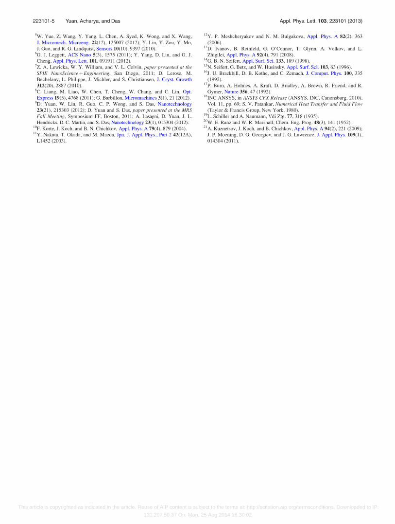
literature.13 Since density of gold is much higher than surround-
ing air, the mass fraction contour alone cannot provide informa-
tion about the hollow nano-structure and the peeling of the
film. Hence the volume fraction contour is drawn for t¼ 4 ns
and t¼ 16 ns in Figs. 7(b) and 7(c). In Fig. 7(c), the presence of
air in the film region explains the peeling of the film from the
substrate and the formation of a hollow nano-structure.
The lowest laser fluence (300 mJ/cm2) resulted in the for-
mation of micro-domes on the film with diameter ranging from
500 nm to 3 lm and height ranging from 50 to 200 nm. An in-
termediate laser fluence (500 mJ/cm2) resulted in the formation
of mushroom structures with diameter ranging from 200 nm to
700 nm and height ranging from 1 to 2 lm. The highest laser
fluence (700 mJ/cm2) allowed a portion of the liquid metal to
separate during recoil and pinch-off, and consequently, sharp
conical peaks were formed with base diameters in the range
100–300 nm, tip heights in the range 1–2.5 lm, and tip diame-
ters around 10 nm. The simulated topography is presented in
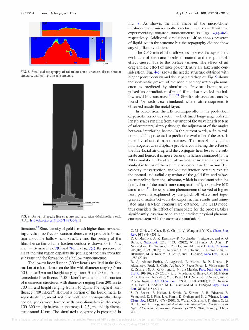
Fig. 8. As shown, the final shape of the micro-dome,
mushroom, and micro-needle structure matches well with the
experimentally obtained nano-structure in Figs. 4(a)–4(c),
respectively. Additional simulation till 40 ns shows presence
of liquid Au in the structure but the topography did not show
any significant variation.
The CFD model also allows us to view the systematic
evolution of the nano-needle formation and the pinch-off
effect caused due to the surface tension. The effect of air
drag and the effect of laser power density are taken into con-
sideration. Fig. 4(c) shows the needle structure obtained with
higher power density and the separated droplet. Fig. 9 shows
the systematic growth of the needle and separation phenom-
enon as predicted by simulation. Previous literature on
pulsed laser irradiation of metal films also revealed the hol-
low shell-like structure.11,13,21 Similar observations can be
found for each case simulated where air entrapment is
observed inside the metal layer.
In conclusion, the LIP technique allows the production
of periodic structures with a well-defined long-range order in
length scales ranging from a quarter of the wavelength to tens
of micrometers, simply through the adjustment of the angles
between interfering beams. In the current work, a finite vol-
ume model is presented to predict the evolution of the experi-
mentally obtained nanostructures. The model solves the
inhomogeneous multiphase problem considering the effect of
the interfacial air drag and the conjugate heat loss to the sub-
strate and hence, it is more general in nature compared to the
MD simulation. The effect of surface tension and air drag is
studied in terms of the resultant nanostructure formation. The
velocity, mass fraction, and volume fraction contours explain
the normal and radial expansion of the gold film and subse-
quent peeling from the substrate, which is consistent with the
predictions of the much more computationally expensive MD
simulation.13 The separation phenomenon observed at higher
laser power is explained by the pinch-off effect and topo-
graphical match between the experimental results and simu-
lated mass fraction contours are obtained. The CFD model
thus considers the effect of atmosphere for the process, takes
significantly less time to solve and predicts physical phenom-
ena consistent with the atomistic simulation.
1C. M. Cobley, J. Chen, E. C. Cho, L. V. Wang, and Y. Xia, Chem. Soc.
Rev. 40(1), 44 (2011).2D. C. Marinica, A. K. Kazansky, P. Nordlander, J. Aizpurua, and A. G.
Borisov, Nano Lett. 12(3), 1333 (2012); W. Husinsky, A. Ajami, P.
Nekvindova, B. Svecova, J. Pesicka, and M. Janecek, Opt. Commun.
285(10), 2729 (2012); P. Genevet, J. P. Tetienne, E. Gatzogiannis, R.
Blanchard, M. A. Kats, M. O. Scully, and F. Capasso, Nano Lett. 10(12),
4880 (2010).3R. A. Alvarez-Puebla, A. Agarwal, P. Manna, B. P. Khanal, P.
Aldeanueva-Potel, E. Carb�o-Argibay, N. Pazos-P�erez, L. Vigderman, E.
R. Zubarev, N. A. Kotov, and L. M. Liz-Marz�an, Proc. Natl. Acad. Sci.
U.S.A. 108(20), 8157 (2011); K. L. Wustholz, A. Henry, J. M. McMahon,
R. G. Freeman, N. Valley, M. E. Piotti, M. J. Natan, G. C. Schatz, and R.
P. Van Duyne, J. Am. Chem. Soc. 132(31), 10903 (2010); E. C. Dreaden,
R. D. Near, T. Abdallah, M. H. Talaat, and M. A. El-Sayed, Appl. Phys.
Lett. 98, 183115 (2011).4S. D. Brown, P. Nativo, J. Smith, D. Stirling, P. R. Edwards, B.
Venugopal, D. J. Flint, J. A. Plumb, D. Graham, and N. J. Wheate, J. Am.
Chem. Soc. 132(13), 4678 (2010); G. Wang, X. Zheng, P. P. Shum, C. Li,
H. Ho, and L. Tong, presented at the 9th International Conference onOptical Communications and Networks (ICOCN 2010), Nanjing, China,
2010.
FIG. 8. Simulated topography of (a) micro-dome structure, (b) mushroom
structure, and (c) micro-needle structure.
FIG. 9. Growth of needle-like structure and separation (Multimedia view).
[URL: http://dx.doi.org/10.1063/1.4833548.1]
223101-4 Yuan, Acharya, and Das Appl. Phys. Lett. 103, 223101 (2013)
This article is copyrighted as indicated in the article. Reuse of AIP content is subject to the terms at: http://scitation.aip.org/termsconditions. Downloaded to IP:
130.207.50.37 On: Mon, 25 Aug 2014 16:30:02
5W. Yue, Z. Wang, Y. Yang, L. Chen, A. Syed, K. Wong, and X. Wang,
J. Micromech. Microeng. 22(12), 125007 (2012); Y. Lin, Y. Zou, Y. Mo,
J. Guo, and R. G. Lindquist, Sensors 10(10), 9397 (2010).6G. J. Leggett, ACS Nano 5(3), 1575 (2011); Y. Yang, D. Lin, and G. J.
Cheng, Appl. Phys. Lett. 101, 091911 (2012).7Z. A. Lewicka, W. Y. William, and V. L. Colvin, paper presented at theSPIE NanoScienceþEngineering, San Diego, 2011; D. Lerose, M.
Bechelany, L. Philippe, J. Michler, and S. Christiansen, J. Cryst. Growth
312(20), 2887 (2010).8C. Liang, M. Liao, W. Chen, T. Cheng, W. Chang, and C. Lin, Opt.
Express 19(5), 4768 (2011); G. Barbillon, Micromachines 3(1), 21 (2012).9D. Yuan, W. Lin, R. Guo, C. P. Wong, and S. Das, Nanotechnology
23(21), 215303 (2012); D. Yuan and S. Das, paper presented at the MRSFall Meeting, Symposium FF, Boston, 2011; A. Lasagni, D. Yuan, J. L.
Hendricks, D. C. Martin, and S. Das, Nanotechnology 23(1), 015304 (2012).10F. Korte, J. Koch, and B. N. Chichkov, Appl. Phys. A 79(4), 879 (2004).11Y. Nakata, T. Okada, and M. Maeda, Jpn. J. Appl. Phys., Part 2 42(12A),
L1452 (2003).
12Y. P. Meshcheryakov and N. M. Bulgakova, Appl. Phys. A 82(2), 363
(2006).13D. Ivanov, B. Rethfeld, G. O’Connor, T. Glynn, A. Volkov, and L.
Zhigilei, Appl. Phys. A 92(4), 791 (2008).14G. B. N. Seifert, Appl. Surf. Sci. 133, 189 (1998).15N. Seifert, G. Betz, and W. Husinsky, Appl. Surf. Sci. 103, 63 (1996).16J. U. Brackbill, D. B. Kothe, and C. Zemach, J. Comput. Phys. 100, 335
(1992).17P. Burn, A. Holmes, A. Kraft, D. Bradley, A. Brown, R. Friend, and R.
Gymer, Nature 356, 47 (1992).18INC ANSYS, in ANSYS CFX Release (ANSYS, INC, Canonsburg, 2010),
Vol. 11, pp. 69; S. V. Patankar, Numerical Heat Transfer and Fluid Flow(Taylor & Francis Group, New York, 1980).
19L. Schiller and A. Naumann, Vdi Ztg. 77, 318 (1935).20W. E. Ranz and W. R. Marshall, Chem. Eng. Prog. 48(3), 141 (1952).21A. Kuznetsov, J. Koch, and B. Chichkov, Appl. Phys. A 94(2), 221 (2009);
J. P. Moening, D. G. Georgiev, and J. G. Lawrence, J. Appl. Phys. 109(1),
014304 (2011).
223101-5 Yuan, Acharya, and Das Appl. Phys. Lett. 103, 223101 (2013)
This article is copyrighted as indicated in the article. Reuse of AIP content is subject to the terms at: http://scitation.aip.org/termsconditions. Downloaded to IP:
130.207.50.37 On: Mon, 25 Aug 2014 16:30:02


