Embed Size (px)
Citation preview
FUL
www.MaterialsViews.comwww.afm-journal.de
Conductive Nanostructures of MMX Chains
LPAPER
By Alejandro Guijarro, Oscar Castillo, Lorena Welte, Arrigo Calzolari,
Pablo J. Sanz Miguel, Carlos J. Gomez-Garcıa, David Olea, Rosa di Felice,
Julio Gomez-Herrero, and Felix Zamora*
Crystals of [Pt2(n-pentylCS2)4I] show a transition from semiconductor to
metallic with the increase of the temperature (conductivity is 0.3–1.4 S � cm�1
at room temperature) and a second metallic–metallic transition at 330 K,
inferred by electrical conductivity measurements. X-ray diffraction studies
carried out at different temperatures (100, 298, and 350 K) confirm the
presence of three different phases. The valence-ordering of these phases is
analyzed using structural, magnetic, and electrical data. Density functional
theory calculations allow a further analysis of the band structure derived for
each phase. Nanostructures adsorbed on an insulating surface show
electrical conductivity. These results suggest that MMX-polymer-based
nanowires could be suitable for device applications.
1. Introduction
Among other building blocks, nanoelectronics require molecularwires capable of transporting electrical charges over reasonablylong distances. In addition, these molecules will need otherfeatures to be useful in nanoelectronics, such as enough stabilityand easy synthesis andmanipulation. Evenmore importantly, theyshould be able to generate nanostructures by means of self-assembly. Several candidates have been tested so far, with carbonnanotubes currently being the most promising choice fornanoelectronic implementation.[1] However, it is well known that
[*] Dr. F. Zamora, A. Guijarro, L. Welte, Dr. P. J. Sanz MiguelDepartamento de Quımica InorganicaUniversidad Autonoma de Madrid28049 Madrid (Spain)E-mail: [email protected]
Dr. O. CastilloDepartamento de Quımica InorganicaFacultad de Ciencia y TecnologıaUniversidad del Paıs Vasco, Apartado 644E–48080 Bilbao (Spain)
Dr. A. Calzolari, Dr. R. di FeliceCentro S3, CNR Istituto di NanoscienzeI-41100 Modena (Italy)
Prof. C. J. Gomez-GarcıaICMol. Parque Cientıfico de la Universidad de Valencia46980 Paterna, Valencia (Spain)
Dr. D. Olea, Prof. J. Gomez-HerreroDepartamento de Fısica de la Materia CondensadaUniversidad Autonoma de Madrid 28049Madrid (Spain)
DOI: 10.1002/adfm.200901901
Adv. Funct. Mater. 2010, 20, 1451–1457 � 2010 WILEY-VCH Verlag GmbH & Co. KGaA
carbon nanotubes still present severalproblems related to their synthesis, chemi-cal functionalization, and organization,which hinder their widespread applicationin nanotechnology.[2] The other side of thecoin is DNA, which has fantastic organiza-tion capabilities but controversial electricaltransport properties.[3,4]
We investigated coordination polymersas an attractive alternative to nanowires,since they may have both conductivity andself-organization. Some mixed-valencemetal–organic systems show unusual elec-tronic properties.[5,6] A paradigmatic case isthat of quasi-1D halogen-bridged mixed-valence binuclear metal complexes, so-
called MMX chains, that can be described as 1D chains ofdimetallic subunits, with the metal ions in mixed-valence states,bridged by halides. The chains within the crystal are packed byweak van derWaals forces, conferring 1Dproperties to the system.[Pt2(RCS2)4I] (R¼ alkyl group) polymers, a particularMMXfamily,have attracted considerable attention because they presentexcellent electrical conductivity in the solid phase (crystals).[7–11]
Recently, we have been able to adsorb nanometer-scale singlemolecules and thick bundles of coordination polymers onsurfaces, showing their potential as molecular wires.[12–15]
Direct sublimation from crystals of coordination polymers andMMX has demonstrated to be a suitable procedure to formnanostructures on surfaces.[16,17] Inparticularwehavebeen able toisolate nanoribbons of [Pt2(dta)4I] (dta¼ dithioacetate) on micaand to prove their excellent electrical conductive properties.[16] Inthis work, we present a complete electrical characterization of[Pt2(n-pentylCS2)4I] complemented with a full structural X-rayanalysis at different temperatures and detailed density functionaltheory (DFT) calculations, allowing confirmation of the differentvalence-ordering states. Theelectrical properties of this compoundhave prompted us to study their electrical transport properties onisolated nanostructures obtained on an insulating surface. Themethod used to form these nanostructures is a simple andstraightforward procedure towards potential technological appli-cations that is based on the self-assembly of the building blocksgenerated in solution.
2. Results and Discussion
Direct current (DC) electrical conductivity measurements per-formed on eight different single crystals of [Pt2(n-pentylCS2)4I] (1)
, Weinheim 1451
FULLPAPER
www.afm-journal.dewww.MaterialsViews.com
1452
show, in all cases, room temperature conductivities in the range0.3–1.4 S � cm�1, similar to that previously reported for the samecompound (s¼ 0.84 S � cm�1)[18] and slightly lower than thosereported in the related [Pt2(RCS2)4I] compounds (17–83, 5–30, and13 S � cm�1 for R¼ n-But, Et, and Me, respectively).[9–11] Twodifferent sequenceswereused for the conductivitymeasurements.
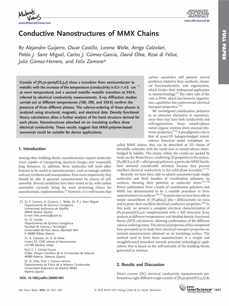
In the first sequence, the crystals were cooled from 300 to 100Kand then warmed to 300K. The cooling run shows a metallicbehavior with a roundedminimumat around 255–270K, followedby an abrupt increase at ca. 200 K (Figs. 1 and S3). This sharpmetal–insulator (M–I) transition is observed at a temperatureslightly lower than that reported for the same compound fromheatcapacitymeasurements (207.4� 0.2 K).[18] The thermally activatedregime follows the 1D variable range hopping model (1D–VRH;s¼ s0
�exp[�(T0/T)1/2]; inset in Fig. S3) used to explain con-
ductivity in many conducting polymers.[19–21] This suggeststhat the conductivity in compound 1 is mainly 1D, as expectedfrom its chain structure. This model, however, cannotreproduce the conductivity in the intermediate temperature range225<T< 255K, which suggests the presence of an intermediateregime between the metallic and the semiconducting regimes, asconfirmed by the smooth change in the DC resistivity. In thisintermediate regime, the coexistence ofmetallic and semiconduct-ing regimesmay be attributed to a progressive distortion of thePt-Idistance along the chain, as already observed in the related[Pt2(EtCS2)4I] compound.[10] After cooling the samples below200K, they were warmed up but the samples did not recover theoriginal resistivity values, suggesting that the M–I transition isaccompanied by important structural changes leading to possiblemicrocracks of the crystals or other plastic deformations that areresponsible for the permanent insulating character after thewholethermal process.
In the secondsequence, fourdifferent crystalswereheated from300 to 400K and then cooled to 100K, followed by a final heatingscan from 100 to 400K. The first heating scan shows a metallicbehavior from 300 to 400Kwith a transition (RT–HT, where RT isroom temperature andHT is a high temperature) that appears as adrop in the resistivity with a negative peak in the derivative at 330 K(inset in Fig. 1). Above this RT–HT transition, the sample recovers
Figure 1. Thermal variation of the electrical resistivity of 1. The dashed line
shows the behavior of a non-heated sample. The inset shows the derivative
of the resistivity as a function of the temperature around the RT–HT
transition.
� 2010 WILEY-VCH Verlag GmbH & C
its metallic character and reaches a resistivity of ca. 7V � cm at400K. The transition at 330K has also been observed in heatcapacity measurements, although at a temperature of 324K, andhas been attributed to a moderate disorder of the alkyl chains.[18]
When the temperature is decreased from 400 to 100K, theresistivity smoothly increases to reach a maximum at ca. 390 K(Fig. 1) followedbymetallic behavior from390Kdown to ca. 290K,where it shows a roundedminimum, similar to that shown by thenon-heated crystals, although at a higher temperature. Thisbehavior confirms the irreversibility of the RT–HT transition,which is also observed in the heat capacity measurements. Belowca. 290 K, the conductivity is again activated and behaves similarlyto the non-heated samples in the 200–240K range. The heatedcrystals also show an abrupt M–I transition at ca. 200K and afterthis transition, the crystals again suffered important microcracksand show a resistivity 103–104 times higher than that observedbefore the transition.
Different types of extreme valence-ordering states have beenconfirmed, depending on the charge states of the metal atoms inthe polymers:[22] i) an averaged-valence state (AV): � � �Mþ2.5 –Mþ2.5 — X — Mþ2.5 – Mþ2.5 — X � � � , ii) a charge polarizationstate (CP): � � �Mþ2 – Mþ3 – X — Mþ2 – Mþ3 – X � � � , iii) a chargedensity wave state (CDW): � � �Mþ2 – Mþ2 — X – Mþ3 – Mþ3 –X � � � , and iv) an alternate charge polarization state (ACP): � � �Mþ2 –Mþ3 – X – Mþ3 – Mþ2 — X � � � .
TheAVandCPstates, inwhich theperiodicity of the chain isM–M–X–, are consistent with a metallic and a Mott–Hubbardsemiconducting state, respectively. The CDW and ACP states,described as Peierls and spin-Peierls states, are sensitive tostructural parameters, and have a doubled M–M–X–M–M–Xperiodicity unit. Recent studies carried out with differentalkyldithiocarboxylate ligands have demonstrated that the lengthof the alkyl chain determines the phase stabilization. As a result,based onphysicalmeasurements, threephases have been reportedfor the [Pt2(n-RCS2)4I]n (R¼ butyl and pentyl): AV (above 324K),ACP (below 210–207K), and an unusual AV state with threefoldPt–Pt–I unit-repetition (between 210 and 324K).[11,23] However,despite its obvious interest, no structural data have been reportedto date for the [Pt2(n-pentylCS2)4I] derivative.
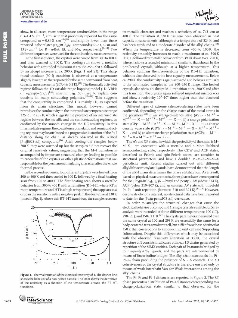
In order to analyze the structural changes that cause theelectrical behavior of compound 1, single crystals suitable forX-rayanalysis were recorded at three different temperatures: 100 (LT),298 (RT), and350 (HT)K.[24] Thecrystal parametersmeasuredoverthe same crystal at 100 and 298K are essentially the same for abody-centered tetragonalunit cell, but differ fromthoseobtainedat350K that corresponds to a monoclinic unit cell (see SupportingInformation). Despite this difference, which may be associatedwith the observed resistivity alteration at 330K, the crystalstructure of 1 consists in all cases of linear 1D chains generated byrepetition of theMMX entities. Each pair of Pt atoms is bridged byfour n-pentyl-CS2 ligands, and the pairs are interconnected bymeans of linear iodine bridges. The alkyl chain surrounds the Pt–Pt–I– chain precluding the presence of S � � � S contacts. The 3Dcohesiveness of the crystal structure is therefore ensured only bymeans of weak interchain Van der Waals interactions among thealkyl chains.
The Pt–Pt and Pt–I distances are reported in Figure 2. The RTphase presents a distribution of Pt–I distances corresponding to acharge-polarization state, similar to that observed for the
o. KGaA, Weinheim Adv. Funct. Mater. 2010, 20, 1451–1457
FULLPAPER
www.MaterialsViews.comwww.afm-journal.de
Figure 2. View of the polymeric [Pt2(n-pentylCS2)4I] chain (top) and bond
distances distribution along the chain at different temperatures (bottom).
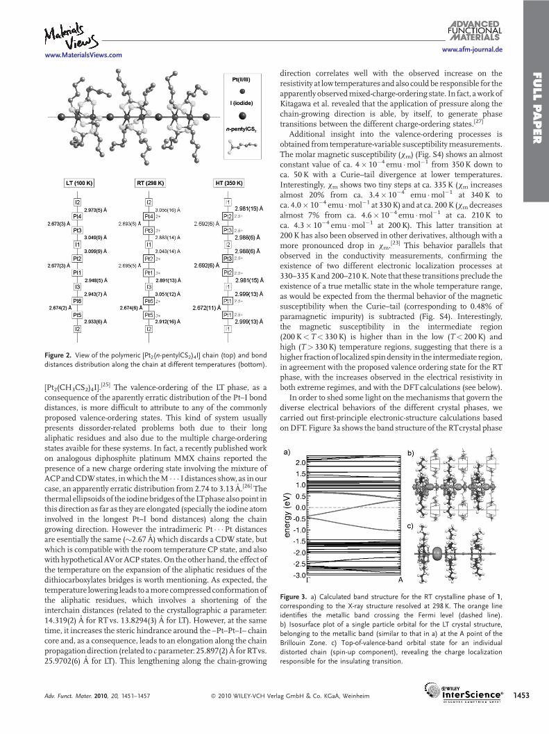
Figure 3. a) Calculated band structure for the RT crystalline phase of 1,
corresponding to the X-ray structure resolved at 298 K. The orange line
identifies the metallic band crossing the Fermi level (dashed line).
b) Isosurface plot of a single particle orbital for the LT crystal structure,
belonging to the metallic band (similar to that in a) at the A point of the
Brillouin Zone. c) Top-of-valence-band orbital state for an individual
distorted chain (spin-up component), revealing the charge localization
responsible for the insulating transition.
[Pt2(CH3CS2)4I].[25] The valence-ordering of the LT phase, as a
consequence of the aparently erratic distribution of the Pt–I bonddistances, is more difficult to attribute to any of the commonlyproposed valence-ordering states. This kind of system usuallypresents dissorder-related problems both due to their longaliphatic residues and also due to the multiple charge-orderingstates avaible for these systems. In fact, a recently published workon analogous diphosphite platinum MMX chains reported thepresence of a new charge ordering state involving the mixture ofACPandCDWstates, inwhich theM � � � I distances show, as in ourcase, an apparently erratic distribution from 2.74 to 3.13 A.[26] Thethermal ellipsoids of the iodinebridges of theLTphase alsopoint inthis direction as far as they are elongated (specially the iodine atominvolved in the longest Pt–I bond distances) along the chaingrowing direction. However the intradimeric Pt � � �Pt distancesare esentially the same (�2.67 A) which discards a CDWstate, butwhich is compatible with the room temperature CP state, and alsowith hypotheticalAVorACPstates.On the other hand, the effect ofthe temperature on the expansion of the aliphatic residues of thedithiocarboxylates bridges is worth mentioning. As expected, thetemperature lowering leads to amorecompressedconformationofthe aliphatic residues, which involves a shortening of theinterchain distances (related to the crystallographic a parameter:14.319(2) A for RT vs. 13.8294(3) A for LT). However, at the sametime, it increases the steric hindrance around the –Pt–Pt–I– chaincore and, as a consequence, leads to an elongation along the chainpropagationdirection (related to cparameter: 25.897(2) A forRTvs.25.9702(6) A for LT). This lengthening along the chain-growing
Adv. Funct. Mater. 2010, 20, 1451–1457 � 2010 WILEY-VCH Verl
direction correlates well with the observed increase on theresistivity at low temperatures andalso could be responsible for theapparently observedmixed-charge-ordering state. In fact, awork ofKitagawa et al. revealed that the application of pressure along thechain-growing direction is able, by itself, to generate phasetransitions between the different charge-ordering states.[27]
Additional insight into the valence-ordering processes isobtained from temperature-variable susceptibilitymeasurements.The molar magnetic susceptibility (xm) (Fig. S4) shows an almostconstant value of ca. 4� 10�4 emu �mol�1 from 350K down toca. 50K with a Curie–tail divergence at lower temperatures.Interestingly, xm shows two tiny steps at ca. 335K (xm increasesalmost 20% from ca. 3.4� 10�4 emu �mol�1 at 340 K toca. 4.0� 10�4 emu �mol�1 at 330 K) and at ca. 200 K (xmdecreasesalmost 7% from ca. 4.6� 10�4 emu �mol�1 at ca. 210K toca. 4.3� 10�4 emu �mol�1 at 200 K). This latter transition at200K has also been observed in other derivatives, although with amore pronounced drop in xm.
[23] This behavior parallels thatobserved in the conductivity measurements, confirming theexistence of two different electronic localization processes at330–335K and 200–210K.Note that these transitions preclude theexistence of a true metallic state in the whole temperature range,as would be expected from the thermal behavior of the magneticsusceptibility when the Curie–tail (corresponding to 0.48% ofparamagnetic impurity) is subtracted (Fig. S4). Interestingly,the magnetic susceptibility in the intermediate region(200K<T< 330K) is higher than in the low (T< 200K) andhigh (T> 330K) temperature regions, suggesting that there is ahigher fractionof localized spindensity in the intermediate region,in agreement with the proposed valence ordering state for the RTphase, with the increases observed in the electrical resistivity inboth extreme regimes, and with the DFTcalculations (see below).
In order to shed some light on the mechanisms that govern thediverse electrical behaviors of the different crystal phases, wecarried out first-principle electronic-structure calculations basedonDFT. Figure 3a shows the band structure of the RTcrystal phase
ag GmbH & Co. KGaA, Weinheim 1453
FULLPAPER
www.afm-journal.dewww.MaterialsViews.com
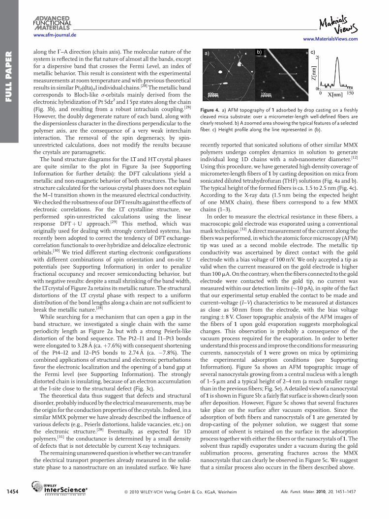
Figure 4. a) AFM topography of 1 adsorbed by drop casting on a freshly
cleaved mica substrate: over a micrometer-length well-defined fibers are
clearly resolved. b) A zoomed area showing the typical features of a selected
fiber. c) Height profile along the line represented in (b).
1454
along the G–A direction (chain axis). The molecular nature of thesystem is reflected in the flat nature of almost all the bands, exceptfor a dispersive band that crosses the Fermi Level, an index ofmetallic behavior. This result is consistent with the experimentalmeasurements at room temperature andwith previous theoreticalresults in similar Pt2(dta)4I individual chains.
[28] Themetallic bandcorresponds to Bloch-like s-orbitals mainly derived from theelectronic hybridization of Pt 5dz2 and I 5pz states along the chain(Fig. 3b), and resulting from a robust intrachain coupling.[28]
However, the doubly degenerate nature of each band, along withthe dispersionless character in the directions perpendicular to thepolymer axis, are the consequence of a very weak interchaininteraction. The removal of the spin degeneracy, by spin-unrestricted calculations, does not modify the results becausethe crystals are paramagnetic.
The band structure diagrams for the LT and HT crystal phasesare quite similar to the plot in Figure 3a (see SupportingInformation for further details): the DFT calculations yield ametallic and non-magnetic behavior of both structures. The bandstructure calculated for the various crystal phases does not explainthe M–I transition shown in the measured electrical conductivity.We checked the robustness of ourDFTresults against the effects ofelectronic correlations. For the LT crystalline structure, weperformed spin-unrestricted calculations using the linearresponse DFTþU approach.[29] This method, which wasoriginally used for dealing with strongly correlated systems, hasrecently been adopted to correct the tendency of DFT exchange-correlation functionals to over-hybridize and delocalize electronicorbitals.[30] We tried different starting electronic configurationswith different combinations of spin orientation and on-site Upotentials (see Supporting Information) in order to penalizefractional occupancy and recover semiconducting behavior, butwith negative results: despite a small shrinking of the band width,the LTcrystal of Figure 2a retains itsmetallic nature. The structuraldistortions of the LT crystal phase with respect to a uniformdistribution of the bond lengths along a chain are not sufficient tobreak the metallic nature.[28]
While searching for a mechanism that can open a gap in theband structure, we investigated a single chain with the sameperiodicity length as Figure 2a but with a strong Peierls-likedistortion of the bond sequence. The Pt2–I1 and I1–Pt3 bondswere elongated to 3.28 A (ca.þ7.6%) with consequent shorteningof the Pt4–I2 and I2–Pt5 bonds to 2.74 A (ca. �7.8%). Thecombined applications of structural and electronic perturbationsfavor the electronic localization and the opening of a band gap atthe Fermi level (see Supporting Information). The stronglydistorted chain is insulating, because of an electron accumulationat the I-site close to the structural defect (Fig. 3c).
The theoretical data thus suggest that defects and structuraldisorder, probably inducedby theelectricalmeasurements,maybethe origin for the conduction properties of the crystals. Indeed, in asimilar MMX polymer we have already described the influence ofvarious defects (e.g., Peierls distortions, halide vacancies, etc.) onthe electronic structure.[28] Eventually, as expected for 1Dpolymers,[31] the conductance is determined by a small densityof defects that is not detectable by current X-ray techniques.
The remainingunansweredquestion iswhetherwe can transferthe electrical transport properties already measured in the solid-state phase to a nanostructure on an insulated surface. We have
� 2010 WILEY-VCH Verlag GmbH & C
recently reported that sonicated solutions of other similar MMXpolymers undergo complex dynamics in solution to generateindividual long 1D chains with a sub-nanometer diameter.[12]
Using this procedure, we have generated high-density coverage ofmicrometer-length fibers of 1 by casting deposition on mica fromsonicated diluted tetrahydrofuran (THF) solutions (Fig. 4a and b).The typical height of the formed fibers is ca. 1.5 to 2.5 nm (Fig. 4c).According to the X-ray data (1.5 nm being the expected heightof one MMX chain), these fibers correspond to a few MMXchains (1–3).
In order to measure the electrical resistance in these fibers, amacroscopic gold electrode was evaporated using a conventionalmask technique.[32] A directmeasurement of the current along thefiberswasperformed, inwhich theatomic forcemicroscopy (AFM)tip was used as a second mobile electrode. The metallic tipconductivity was ascertained by direct contact with the goldelectrode with a bias voltage of 100mV. We only accepted a tip asvalid when the current measured on the gold electrode is higherthan100mA.Onthecontrary,when thefibers connected to thegoldelectrode were contacted with the gold tip, no current wasmeasured within our detection limits (�10 pA), in spite of the factthat our experimental setup enabled the contact to be made andcurrent–voltage (I–V) characteristics to be measured at distancesas close as 50 nm from the electrode, with the bias voltageranging� 8V. Closer topographic analysis of the AFM images ofthe fibers of 1 upon gold evaporation suggests morphologicalchanges. This observation is probably a consequence of thevacuum process required for the evaporation. In order to betterunderstand thisprocess and improve theconditions formeasuringcurrents, nanocrystals of 1 were grown on mica by optimizingthe experimental adsorption conditions (see SupportingInformation). Figure 5a shows an AFM topographic image ofseveral nanocrystals growing from a central nucleus with a lengthof 1–5mm and a typical height of 2–4 nm (a much smaller rangethan in thepreviousfibers; Fig. 5e). Adetailed viewof ananocrystalof 1 is shown inFigure 5b: a fairly flat surface is shown clearly soonafter deposition. However, Figure 5c shows that several fracturestake place on the surface after vacuum exposition. Since theadsorption of both fibers and nanocrystals of 1 are generated bydrop-casting of the polymer solution, we suggest that someamount of solvent is retained on the surface in the adsorptionprocess together with either the fibers or the nanocrystals of 1. Thesolvent thus rapidly evaporates under a vacuum during the goldsublimation process, generating fractures across the MMXnanocrystals that can clearly be observed in Figure 5c. We suggestthat a similar process also occurs in the fibers described above.
o. KGaA, Weinheim Adv. Funct. Mater. 2010, 20, 1451–1457
FULLPAPER
www.MaterialsViews.comwww.afm-journal.de
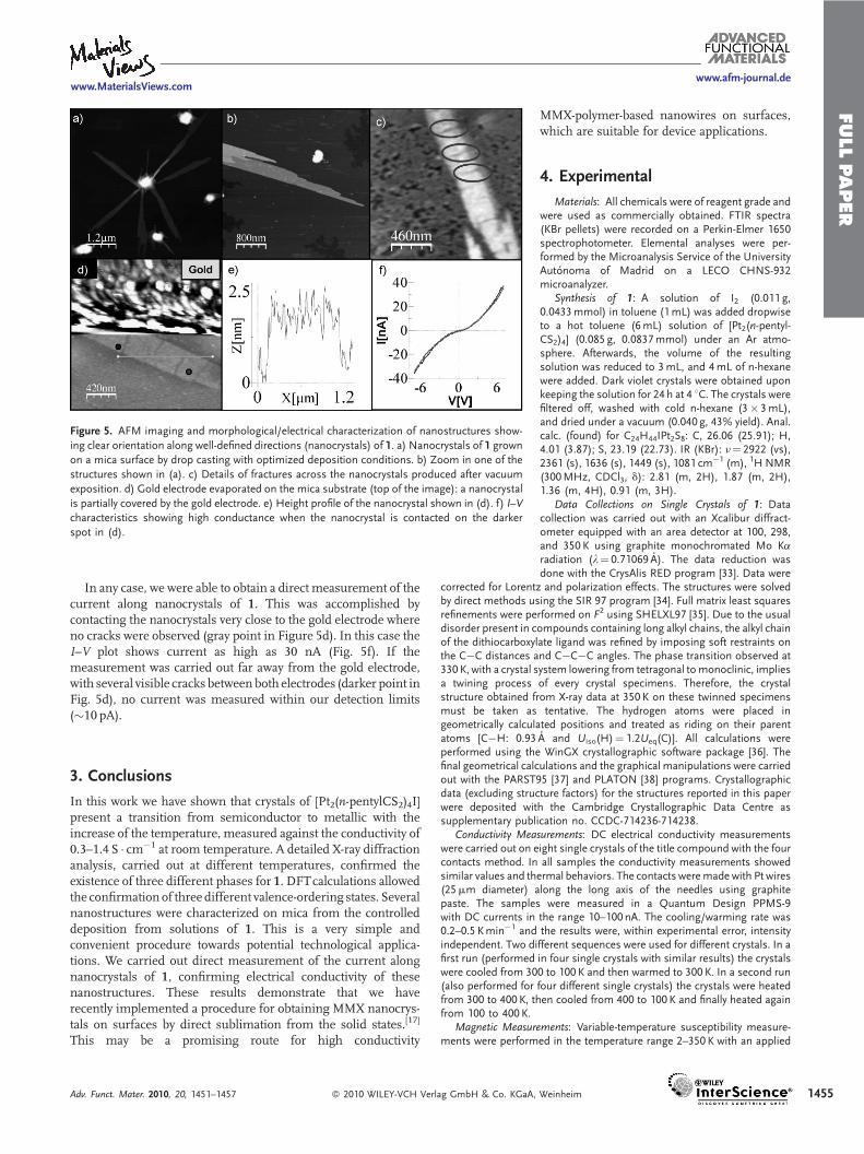
Figure 5. AFM imaging and morphological/electrical characterization of nanostructures show-
ing clear orientation along well-defined directions (nanocrystals) of 1. a) Nanocrystals of 1 grownon a mica surface by drop casting with optimized deposition conditions. b) Zoom in one of the
structures shown in (a). c) Details of fractures across the nanocrystals produced after vacuum
exposition. d) Gold electrode evaporated on the mica substrate (top of the image): a nanocrystal
is partially covered by the gold electrode. e) Height profile of the nanocrystal shown in (d). f) I–V
characteristics showing high conductance when the nanocrystal is contacted on the darker
spot in (d).
In any case, we were able to obtain a direct measurement of thecurrent along nanocrystals of 1. This was accomplished bycontacting the nanocrystals very close to the gold electrode whereno cracks were observed (gray point in Figure 5d). In this case theI–V plot shows current as high as 30 nA (Fig. 5f). If themeasurement was carried out far away from the gold electrode,with several visible cracks between both electrodes (darker point inFig. 5d), no current was measured within our detection limits(�10 pA).
3. Conclusions
In this work we have shown that crystals of [Pt2(n-pentylCS2)4I]present a transition from semiconductor to metallic with theincrease of the temperature, measured against the conductivity of0.3–1.4 S � cm�1 at room temperature. A detailed X-ray diffractionanalysis, carried out at different temperatures, confirmed theexistence of three different phases for 1. DFTcalculations allowedthe confirmation of three different valence-ordering states. Severalnanostructures were characterized on mica from the controlleddeposition from solutions of 1. This is a very simple andconvenient procedure towards potential technological applica-tions. We carried out direct measurement of the current alongnanocrystals of 1, confirming electrical conductivity of thesenanostructures. These results demonstrate that we haverecently implemented a procedure for obtaining MMX nanocrys-tals on surfaces by direct sublimation from the solid states.[17]
This may be a promising route for high conductivity
Adv. Funct. Mater. 2010, 20, 1451–1457 � 2010 WILEY-VCH Verlag GmbH & Co. KGaA,
MMX-polymer-based nanowires on surfaces,which are suitable for device applications.
4. Experimental
Materials: All chemicals were of reagent grade andwere used as commercially obtained. FTIR spectra(KBr pellets) were recorded on a Perkin-Elmer 1650spectrophotometer. Elemental analyses were per-formed by the Microanalysis Service of the UniversityAutonoma of Madrid on a LECO CHNS-932microanalyzer.
Synthesis of 1: A solution of I2 (0.011 g,0.0433mmol) in toluene (1mL) was added dropwiseto a hot toluene (6mL) solution of [Pt2(n-pentyl-CS2)4] (0.085 g, 0.0837mmol) under an Ar atmo-sphere. Afterwards, the volume of the resultingsolution was reduced to 3mL, and 4mL of n-hexanewere added. Dark violet crystals were obtained uponkeeping the solution for 24 h at 4 8C. The crystals werefiltered off, washed with cold n-hexane (3� 3mL),and dried under a vacuum (0.040 g, 43% yield). Anal.calc. (found) for C24H44IPt2S8: C, 26.06 (25.91); H,4.01 (3.87); S, 23.19 (22.73). IR (KBr): n¼ 2922 (vs),2361 (s), 1636 (s), 1449 (s), 1081 cm�1 (m), 1H NMR(300MHz, CDCl3, d): 2.81 (m, 2H), 1.87 (m, 2H),1.36 (m, 4H), 0.91 (m, 3H).
Data Collections on Single Crystals of 1: Datacollection was carried out with an Xcalibur diffract-ometer equipped with an area detector at 100, 298,and 350 K using graphite monochromated Mo Karadiation (l¼ 0.71069 A). The data reduction wasdone with the CrysAlis RED program [33]. Data were
corrected for Lorentz and polarization effects. The structures were solvedby direct methods using the SIR 97 program [34]. Full matrix least squaresrefinements were performed on F2 using SHELXL97 [35]. Due to the usualdisorder present in compounds containing long alkyl chains, the alkyl chainof the dithiocarboxylate ligand was refined by imposing soft restraints onthe C�C distances and C�C�C angles. The phase transition observed at330 K, with a crystal system lowering from tetragonal tomonoclinic, impliesa twining process of every crystal specimens. Therefore, the crystalstructure obtained from X-ray data at 350 K on these twinned specimensmust be taken as tentative. The hydrogen atoms were placed ingeometrically calculated positions and treated as riding on their parentatoms [C�H: 0.93 A and Uiso(H)¼ 1.2Ueq(C)]. All calculations wereperformed using the WinGX crystallographic software package [36]. Thefinal geometrical calculations and the graphical manipulations were carriedout with the PARST95 [37] and PLATON [38] programs. Crystallographicdata (excluding structure factors) for the structures reported in this paperwere deposited with the Cambridge Crystallographic Data Centre assupplementary publication no. CCDC-714236-714238.
Conductivity Measurements: DC electrical conductivity measurementswere carried out on eight single crystals of the title compound with the fourcontacts method. In all samples the conductivity measurements showedsimilar values and thermal behaviors. The contacts weremade with Pt wires(25mm diameter) along the long axis of the needles using graphitepaste. The samples were measured in a Quantum Design PPMS-9with DC currents in the range 10–100nA. The cooling/warming rate was0.2–0.5 Kmin�1 and the results were, within experimental error, intensityindependent. Two different sequences were used for different crystals. In afirst run (performed in four single crystals with similar results) the crystalswere cooled from 300 to 100 K and then warmed to 300 K. In a second run(also performed for four different single crystals) the crystals were heatedfrom 300 to 400 K, then cooled from 400 to 100K and finally heated againfrom 100 to 400K.
Magnetic Measurements: Variable-temperature susceptibility measure-ments were performed in the temperature range 2–350K with an applied
Weinheim 1455
FULLPAPER
www.afm-journal.dewww.MaterialsViews.com
1456
magnetic field of 1 T on a polycrystalline sample of 1 (with a mass of6.235mg) with a Quantum Design MPMS-XL-5 SQUID magnetometer.Only the transition at 200 K was measured in both cooling and warmingscans. Because the signal was very weak and in order to improve thestatistic, up to ten measurements were averaged for each point. Thesusceptibility data were corrected for the sample holder previouslymeasured using the same conditions and for the diamagnetic contribu-tions of the salt as deduced by using Pascal’s constant tables(xdia¼�516� 10�6 emu �mol�1).
AFM: Images were acquired in dynamic mode using a NanotecElectronica system [39]. Olympus cantilevers (RC800PSA (ORC8)) wereused with a nominal force constant of 0.75Nm�1 with a pyramid shapeand <20-nm nominal radius tip. The images were processed using WSxM(freely downloadable SPM software [39]) operating at room temperature inambient air conditions.
Preparation of the Substrates: In order to obtain reproducible results,Muscovite Mica (commercially available) was cleaved with adhesive tapejust before deposition of solutions.
Adsorption of MMX Fibers on Mica: [Pt2(n-pentylCS2)4I]n (1mg) in THF(1mL) was sonicated (544W, 32 kHz) for 1 h at 30 8C. From this mothersolution, diluted solutions of 1� 10�13 g L�1 were prepared. The elutedsolution (10mL) was deposited on a freshly exfoliated Muscovite micasubstrate. The sample was left in air allowing the complete solventevaporation.
Formation of MMX Nanocrystals on Mica: [Pt2(n-pentylCS2)4I]n (1mg)in a 1:1 hexane/toluene solvent mixture (1mL) was sonicated (272W,16 kHz) for 15min at 30 8C. From this mother solution, diluted solutions of0.1 g L�1 were prepared. The eluted solution (10mL) was deposited on afreshly exfoliated Muscovite mica substrate at different times (t¼ 0 andt¼ 24 h). The sample was left in air allowing the complete solventevaporation (Fig. S5).
Electrical Characterization on the Surface: In order to make the electricalcharacterization of the [Pt2(n-pentylCS2)4I]n fibers and nanocrystalsdeposited on mica, a macroscopic gold electrode was evaporated, usinga mask, on the samples at 10�7mbar (high vacuum conditions). The goldelectrode was evaporated applying a current of 6 A during 15min, leaving asharp electrode edge over the sample. Conductive Au/Pd tips wereprepared by sputtering at high vacuum conditions to make theconductance AFM experiments. Topographic AFM images alongthe electrode show polymer chains and nanocrystals partially covered bythe gold electrode (Fig. S6).
DFT Calculations: The ground-state electronic structure of MMXcrystals was obtained via single-point ab initio calculations, based onthe plane-wave ultrasoft-pseudopotential implementation of DFT as in thequantum-espresso software package [40]. The PBE generalized gradientapproximation to the exchange correlation functional was applied. Theenergy cutoffs for wave functions (25 Ry) and charge (250 Ry), as well as thepseudopotential accuracy for single chemical species, were tested andvalidated beforehand [28]. The crystalline structures were simulated bymeans of large periodically repeated supercells, with atomic coordinates(for LT, RT, and HT configurations) and cell sizes taken from theexperimental X-ray data. No further atomic relaxation was imposed [41].For each structure in Figure 2, the unit supercell contained six MMXmonomers assembled in two parallel polymeric chains (474 atoms and1290 electrons). Eight special k-points were used for the charge densitysums in the irreducible wedge of the 3D Brillouin Zone. Explicit treatmentof the spin degree of freedom is considered within the local spin densityapproximation (LSDA). The effects of the electron–electron correlation,beyond standard DFT, were taken into account with the inclusion of localHubbard potentials U, within the LSDAþU scheme. The correlation ofatomic orbitals involves Pt 5d, I 5p, and S 3p partially occupied shells.
Acknowledgements
The authors gratefully acknowledge the financial support of the SpanishMinisterio de Educacion y Ciencia (Projects MAT2007-66476-C01/02,
� 2010 WILEY-VCH Verlag GmbH & C
NAN2004-09183-C10-05/06, and CSD 2007-00010 Consolider-Ingenio),CAM (S-0505/MAT/0303), and the European Union (FP6-029192 DNA-NANODEVICES, ERA in Chemistry Program CTQ2006-027185-E andMAGMANet network of excellence). Calculations were run at super-computers at CINECA, Bologna, Italy. Supporting Information is availableonline from Wiley InterScience or from the author.
Received: October 8, 2009
Published online: March 31, 2010
[1] R. Saito, G. Dresslhauss, M. Dresselhauss, Physical Properties of Carbon
Nanotubes, Imperial College, Bristol 1998.
[2] Physical properties of carbon nanotubes (Eds: M. S Dresselhaus,
G Dresselhaus, P. Avouris), Springer, Berlin 2001.
[3] D. Porath, A. Bezryadin, S. de Vries, C. Dekker, Nature 2000, 403, 635.
[4] P. J. de Pablo, F. Moreno-Herrero, J. Colchero, J. G. Herrero, P. Herrero,
A.M. Baro, P. Ordejon, J. M. Soler, E. Artacho, Phys. Rev. Lett. 2000, 85, 4992.
[5] F. A. Cotton, C. A. Murillo, R. A. Walton, Multiple Bonds Between Metal
Atoms, 3rd ed, Springer, New York 2005.
[6] J. K. Bera, K. R. Dunbar, Angew. Chem. Int. Ed. 2002, 41, 4453.
[7] C. Bellitto, A. Flamini, L. Gastaldi, L. Scaramuzza, Inorg. Chem. 1983, 22,
444.
[8] H. Kitagawa, N. Onodera, J. S. Ahn, T. Mitani, K. Toriumi, M. Yamashita,
Synth. Met. 1997, 86, 1931.
[9] H. Kitagawa, N. Onodera, T. Sonoyama, M. Yamamoto, T. Fukawa,
T. Mitani, M. Seto, Y. Maeda, J. Am. Chem. Soc. 1999, 121, 10068.
[10] M. Mitsumi, T. Murase, H. Kishida, T. Yoshinari, Y. Ozawa, K. Toriumi,
T. Sonoyama, H. Kitagawa, T. Mitani, J. Am. Chem. Soc. 2001, 123, 11179.
[11] M. Mitsumi, K. Kitamura, A. Morinaga, Y. Ozawa, M. Kobayashi,
K. Toriumi, Y. Iso, H. Kitagawa, T. Mitani, Angew. Chem. Int. Ed. 2002,
41, 2767.
[12] L. Welte, R. Gonzalez-Prieto, D. Olea, M. Rosario Torres, J. L. Priego,
R. Jimenez-Aparicio, J. Gomez-Herrero, F. Zamora, ACS Nano 2008, 2,
2051.
[13] E. Mateo-Marti, L. Welte, P. Amo-Ochoa, P. J. S. Miguel, J. Gomez-Herrero,
J. A. Martin-Gago, F. Zamora, Chem. Commun. 2008, 945.
[14] P. Amo-Ochoa, M. I. Rodriguez-Tapiador, O. Castillo, D. Olea, A. Guijarro,
S. S. Alexandre, J. Gomez-Herrero, F. Zamora, Inorg. Chem. 2006, 45, 7642.
[15] D. Olea, S. S. Alexandre, P. Amo-Ochoa, A. Guijarro, F. de Jesus, J. M. Soler,
P. J. de Pablo, F. Zamora, J. Gomez-Herrero, Adv. Mater. 2005, 17, 1761.
[16] L. Welte, A. Calzolari, R. Di Felice, F. Zamora, J. Gomez-Herrero, Nat.
Nanotechnol. 2010, 5, 110.
[17] L. Welte, U. Garcıa-Couceiro, O. Castillo, D. Olea, C. Polop, A. Guijarro,
A. Luque, J. M. Gomez-Rodrıguez, J. Gomez-Herrero, F. Zamora, Adv.
Mater. 2009, 21, 2025.
[18] K. Saito, S. Ikeuchi, Y. Nakazawa, A. Sato, M. Mitsumi, T. Yamashita,
K. Toriumi, M. Sorai, J. Phys. Chem. B 2005, 109, 2956.
[19] V. K. S. Shante, C. M. Varma, A. N. Bloch, Phys. Rev. B 1973, 8, 4885.
[20] Z. H. Wang, C. Li, E. M. Scherr, A. G. Macdiarmid, A. J. Epstein, Phys. Rev.
Lett. 1991, 66, 1745.
[21] Z. H. Wang, E. M. Scherr, A. G. Macdiarmid, A. J. Epstein, Phys. Rev. B 1992,
45, 4190.
[22] Y. Wakabayashi, A. Kobayashi, H. Sawa, H. Ohsumi, N. Ikeda, H. Kitagawa,
J. Am. Chem. Soc. 2006, 128, 6676.
[23] H. Tanaka, S. Kuroda, T. Yamashita, M. Mitsumi, K. Toriumi, J. Phys. Soc.
Jpn. 2003, 72, 2169.
[24] Crystallographic data and refinement parameters for 1 at 100K: cryst syst,
tetragonal; space group, I4; a¼ b¼ 13.8294(3) A; c¼ 25.9702(6) A;
V¼ 4966.86(19) A3; Z¼ 6; Dcalcd¼ 2.219 g cm�3; m¼ 9.894mm�1;
F(000)¼ 3150; cryst size¼ 0.18T 0.02T 0.02mm3; u range for data
collection, 2.78- to 27.10-; reflens collected, 13279; independent reflns,
4921 (Rint¼ 0.0334); parameters, 142; R1(Fo)¼ 0.0401 [I > 2s(I)], wR2
(F2o)¼ 0.0982 [I > 2s(I)]; GOF on F2, 0.915. For 1 at 298K: cryst syst,
tetragonal; space group, I4; a¼ b¼ 14.319(2) A; c¼ 25.897(2) A;
V¼ 5309.8(11) A3; Z¼ 6; Dcalcd¼ 2.076 g cm�3; m¼ 9.253mm�1;
o. KGaA, Weinheim Adv. Funct. Mater. 2010, 20, 1451–1457
FULLPAPER
www.MaterialsViews.comwww.afm-journal.de
F(000)¼ 3150; cryst size¼ 0.18T 0.02T 0.02mm3; u range for data col-
lection, 2.55- to 25.03-; reflens collected, 8257; independent reflns, 3482
(Rint¼ 0.0809); parameters, 142; R1(Fo)¼ 0.0555 [I > 2s(I)], wR2
(F2o)¼ 0.1282 [I > 2s(I)]; GOF on F2, 0.720. For 1 at 350 K: cryst syst,
monoclinic; space group, C2/m; a¼ 18.920(5) A; b¼ 25.992(3) A;
c¼ 14.306(3) A; V¼ 5419.1(19) A3; Z¼ 6; Dcalcd¼ 2.033 g cm�3; m¼9.064mm�1; F(000)¼ 3150; cryst size¼ 0.23T 0.18T 0.07mm3;
u range for data collection, 3.21- to 29.23-; reflens collected, 20956;
independent reflns, 7506 (Rint¼ 0.0809); parameters, 144;
R1(Fo)¼ 0.0759 [I > 2s(I)], wR2 (F2o)¼ 0.1944 [I > 2s(I)]; GOF on F2,
0.651. Common data: empirical formula, C24H44I1Pt2S8; fw¼ 1106.15;
l¼ 0.71073.
[25] M. Yamashita, S. Miya, T. Kawashima, T. Manabe, T. Sonoyama,
H. Kitagawa, T. Mitani, Synth. Met. 1999, 103, 2164.
[26] H. Iguchi, S. Takaishi, T. Kajiwara, H. Miyasaka, M. Yamashita,
H. Matsuzaki, H. Okamoto, J. Am. Chem. Soc. 2008, 130, 17668.
[27] A. Kobayashi, A. Tokunaga, R. Ikeda, H. Sagayama, Y. Wakabayashi,
H. Sawa, M. Hedo, Y. Uwatoko, H. Kitagawa, Eur. J. Inorg. Chem. 2006,
3567.
[28] A. Calzolari, S. S. Alexandre, F. Zamora, R. di Felice, J. Am. Chem. Soc.
2008, 130, 5552.
[29] M. Cococcioni, S. de Gironcoli, Phys. Rev. B 2005, 71, 035105.
[30] D. A. Scherlis, M. Cococcioni, P. Sit, N. Marzari, J. Phys. Chem. B 2007, 111,
7384.
Adv. Funct. Mater. 2010, 20, 1451–1457 � 2010 WILEY-VCH Verl
[31] Metallic chains/Chains of Atoms (Eds: M. Springborg, Y. Dong) Elsevier,
Amsterdam 2007.
[32] P. J. de Pablo, M. T. Martinez, J. Colchero, J. Gomez-Herrero, W. K. Maser,
A. M. Benito, E. Munoz, A. M. Baro, Adv. Mater. 2000, 12, 573.
[33] CrysAlis RED, version 1.170; Oxford Diffraction, Wroclaw, Poland 2003.
[34] A. Altomare, M. C. Burla, M. Camalli, G. L. Cascarano, C. Giacovazzo,
A. Guagliardi, A. G. G. Moliterni, G. Polidori, R. Spagna, J. Appl. Crystallogr.
1999, 32, 115.
[35] G. M. Sheldrick, SHELXL97, University of Gottingen, Germany 1997.
[36] L. J. Farrugia, WINGX. A Windows Program for Crystal Structure Analysis,
University of Glasgow, UK 1998.
[37] M. Nardelli, J. Appl. Crystallogr. 1995, 28, 659.
[38] A. L. Spek, PLATON. A Multipurpose Crystallographic Tool, Utrecht Univer-
sity, Utrecht, Holland 1998.
[39] Nanotec Electronica, www.nanotec.es (accessed February 2010).
[40] P. Giannozzi, S. Baroni, N. Bonini, M. Calandra, R. Car, C. Cavazzoni,
D. Ceresoli, G. L. Chiarotti, M. Cococcioni, I. Dabo, A. Dal Corso, S. de
Gironcoli, S. Fabris, G. Fratesi, R. Gebauer, U. Gerstmann, C. Gougoussis,
A. Kokalj, M. Lazzeri, L. Martin-Samos, N.Marzari, F. Mauri, R. Mazzarello,
S. Paolini, A. Pasquarello, L. Paulatto, C. Sbraccia, S. Scandolo, G. Sclauzero,
A. P. Seitsonen, A. Smogunov, P. Umari, R. M. Wentzcovitch, J. Phys.:
Condens. Matter 2009, 21, 395502.
[41] A. Guijarro, O. Castillo, A. Calzolari, P. J. S. Miguel, C. J. Gomez-Garcia,
R. di Felice, F. Zamora, Inorg. Chem. 2008, 47, 9736.
ag GmbH & Co. KGaA, Weinheim 1457


