Embed Size (px)
Citation preview
Enhancing visibility of graphene on arbitrary substrates by microdroplet condensation
Hugo Gonçalves1, Michael Belsley1, Cacilda Moura1, Tobias Stauber2 and Peter Schellenberg1*1Centro de Física, University of Minho, Campus de Gualtar, Pt - 4710-057 Braga, Portugal2Department of Condensed Matter Physics, University Autónoma of MadridCampus of Cantoblanco, E-28049 Madrid, Spain
Abstract
In order to take advantage of the enormous potential of graphene for
future electronic micro-circuits and other applications it is necessary
to develop reliable, rapid and widely applicable methods to visualize
graphene based structures. We report here on a micro-droplet
condensation technique, which allows for quick visual identification of
graphene on a variety of substrates, including some which were
previously considered unsuitable for the visualization of carbon
layers. The technique should also be applicable to visualize artificially
patterned graphene structures which are expected to be key
technologically enabling components in electronic micro-circuits and
other applications.
* to whom correspondence should be addressed, [email protected]
Monolayer 1-3, bilayer 4 and few layer graphene 5 have attracted
intense research interest in recent years 6,7 due to their unique electronic
transport 8 and elastic 9 properties which allow one to probe a variety of
fundamental questions in physics 10 as well as to enable the potential
development of distinctive nanoelectronic devices 11. While a multitude of
mostly optics based methods have been proposed to identify single and few
atomic layer samples12, the process is a time consuming and tedious task.
For example, interference enhanced reflection contrast due to refractive
index differences between a dielectric layer on a silicon wafer and the
graphene flakes is often used 13-16. Other imaging methods are based on
Raman and Rayleigh scattering 17,18, on fluorescence quenching of dyes by
graphene layers 19, or on ellipsometry 20. All of these methods require
complex equipment or an optimized substrate coating. Here, we report on a
generally applicable and easy to use technique for the identification of
potential graphene flakes by microdroplet condensation. The method is
already well-known in micropatterning for the visualization of surface
features of different hydrophobicities. In particular, this technique is suitable
for making graphene visible in a standard reflection microscope on virtually
any surface including plastics or uncoated metals, for which no method was
previously available 12. Graphene can also be identified on transparent
surfaces in transmission, which is difficult to achieve otherwise, as the
absorption of a graphene monolayer is just 2.3 % of white light 21.
The technique may also be utilized to analyze artificially produced
graphene based micropatterns, such as microelectronic or microoptical
devices as envisioned in recent developments of graphene applications.
Assessing the quality and uniformity of large-area graphene films 22,23 for
use in transparent conductor applications such as flat screens or solar
panels may also become possible.
Upon exhaling onto a simple glass surface, the resulting breath
condensation shows the presence of fatty deposits, due to the difference in
hydrophobicity. This observation was already described by Rayleigh 24, and
was later exploited to investigate microscopic heterogeneities on surfaces,
which resulted in optical condensation images 25-28. The method is capable
of visualizing heterogeneities in self-assembled monolayers 27,29 or natural 30
or artificial 25,31,32 micropatterning of a surface. Regions of different
hydrophobicity result in the appearance of condensation features and the
spatial resolution of this patterning depends on the size of the condensed
microdroplets. In this letter, we show that microdroplet condensation can be
easily applied to readily show single and few-layer graphene flakes on
almost any kind of surface, which would otherwise be difficult to spot.
Apparently, graphene has an especially high hydrophobicity, making it easy
to identify graphene flakes, even when the optical contrast in relation to the
substrate is low or vanishing. The method is particularly suited for
identifying flakes with spatial dimensions of 1 μm or larger, the resolution
depending on the substrate and the vapor used. We have tested a variety of
substrates, including microscope glass slides, adhesion slides (Menzel –
‘Polysine’ and -‘Plus’) as well as silicon and glass wafers spin-coated with a
layer of polymethylmethacrylate (PMMA) 14 or polystyrene (PS). Metal
surfaces such as polished stainless steel and uncoated silicon were also
used. These materials cover a wide range of hydrophobicities and other
surface properties, demonstrating the generality of the technique.
In the experiments, the flakes were deposited by mechanical cleavage
of 2 - 5 mm large natural graphite pieces (NGS Naturgraphit 'graphenium ').
The resulting monolayers were typically 25 – 500 μm2 in size. Sub-
sequently, the polymer coated substrates were cleaned with ethanol and the
uncoated surfaces were cleaned with chloroform to remove glue stains and
other contaminations. The droplet condensation figures are produced by
blowing water 28, Ethyleneglycol (EG) or Diethyleneglycol (DEG) 32 vapor
over the substrate with the graphene flakes immobilized on its surface.
In principle, water droplet condensation figures could be produced by
simply exhaling over the slide surface. To allow for longer viewing times it is
helpful to cool the surface using a peltier element attached below the
sample 31. In order to better control the droplet size and also to permit the
use of different vapors, an apparatus adapted from Schäfle et al 32 was em-
ployed to generate the vapor. In short, nitrogen gas was bubbled through a
gas wash bottle filled with the respective liquid. The gas flowed through the
outlet of a glass tube topped with a fritted glass piece for bubble dispersion,
and the vapor exited via a nozzle. Water vapor was generated at room tem-
perature and blown directly over the slide placed on the microscope stage.
EG and DEG were heated in the same setting to around 70° and 120° C re-
spectively. The slides were fixed at a distance of 40 mm in front of a 5 mm
wide nozzle covered with a sheet of lens tissue to prevent large droplets
from exiting and exposed to the vapor for 10 s, after which the slides were
transferred to the microscope where the droplets remained stable for sever-
al minutes. The observation time could be extended by using a peltier ele-
ment to induce moderate cooling. While DEG was used in the original pub-
lication 32, the usage of EG turned out to be the superior choice in our ex-
periments, as the droplet sizes were more homogeneous and the high DEG
vapor temperature of ~120° C occasionally damaged the graphene flakes.
The droplets typically evaporated, leaving no residue, but the surface could
also be cleaned with an appropriate solvent. The investigations were per-
formed using a Nikon Optiphot metallurgical reflection microscope.
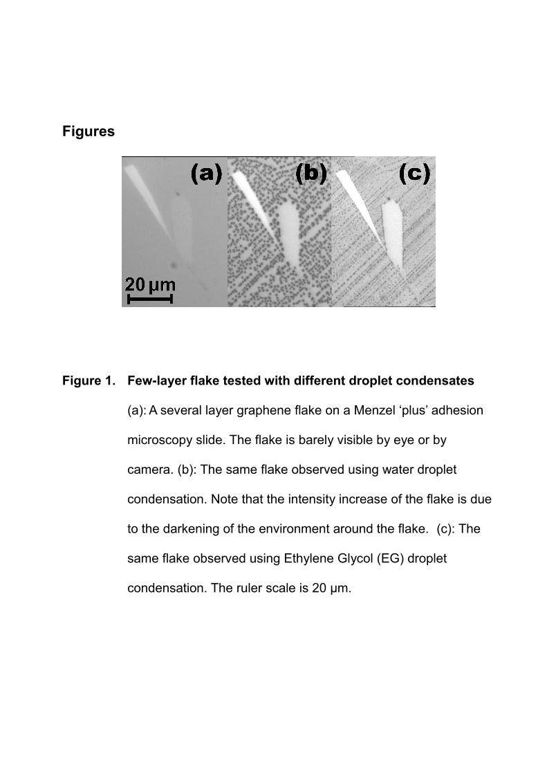
For an illustration of the technique, Fig. 1a shows a graphene flake,
which consists of a few layers of carbon to make it at least faintly visible in
the photograph prior to droplet condensation, and the contrast enhance-
ment due to water (Fig. 1b) or EG (Fig. 1c) droplet condensation. Note that
the presence of the droplets not only delimits the area of the flake, but also
helps to increase the visual contrast by reducing the amount of light collec-
ted from the areas covered by the droplets. Fig. 2 and 3 illustrate the identi-
fication of graphene flakes on glass and metal substrates respectively, that
were virtually invisible prior to droplet condensation and which were sub-
sequently confirmed by Raman microscopy to be monolayers.
Generally, the droplet size is the limiting factor for the spatial resolu-
tion. This in turn depends on the chemical used for vapor generation, on
the details of the vapor preparation and on the substrate surface. Resolu-
tions of roughly 2.5 μm can be obtained for water on glass and PMMA and 1
μm for water on polysine surfaces. The best resolution (0.7 μm) was
achieved by depositing EG on Menzel slide polysine and ‘plus’ surfaces. Al-
though it is not possible to distinguish graphene monolayers from few-layer
sheets by this method, it does allow a quick and easy identification of can-
didate flakes on the slide, which are imperceptible or barely visible by eye.
For an unambiguous determination of the number of layers, we sub-
sequently employed Raman microscopy to investigate each candidate flake
separately.
To conclude, we were able to show that micro-droplet condensation
can be employed to quickly and easily visualize graphene and few-layer
graphite on a wide variety of substrates without the need for any specific
surface modification or preparation. There is no other currently available
method that is capable of readily visualizing graphene flakes on plastic
surfaces 12 and metals. The technique will not only facilitate the identification
of graphene flakes but may also have a great potential for the quick and
non-invasive visualization of artificially patterned structures in graphene-
based devices such as electronic micro-circuits, micro-optical settings and
others.
We thank J. A. Santos for instrumental support and W. Fritzsche, K. S.
Novoselov and N. M. R. Peres for useful discussions. This work has been
supported by FCT under grant PTDC/FIS/101434/2008 and by MIC under
grant FIS2010-21883-C02-02. H.G. received support from FCT, grant no.
BII/UNI/0607/FIS/2009.
Figures
Figure 1. Few-layer flake tested with different droplet condensates
(a): A several layer graphene flake on a Menzel ‘plus’ adhesion
microscopy slide. The flake is barely visible by eye or by
camera. (b): The same flake observed using water droplet
condensation. Note that the intensity increase of the flake is due
to the darkening of the environment around the flake. (c): The
same flake observed using Ethylene Glycol (EG) droplet
condensation. The ruler scale is 20 μm.
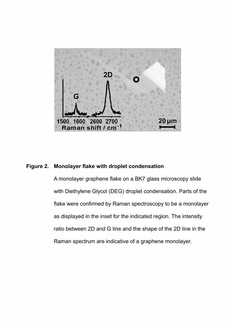
Figure 2. Monolayer flake with droplet condensation
A monolayer graphene flake on a BK7 glass microscopy slide
with Diethylene Glycol (DEG) droplet condensation. Parts of the
flake were confirmed by Raman spectroscopy to be a monolayer
as displayed in the inset for the indicated region. The intensity
ratio between 2D and G line and the shape of the 2D line in the
Raman spectrum are indicative of a graphene monolayer.
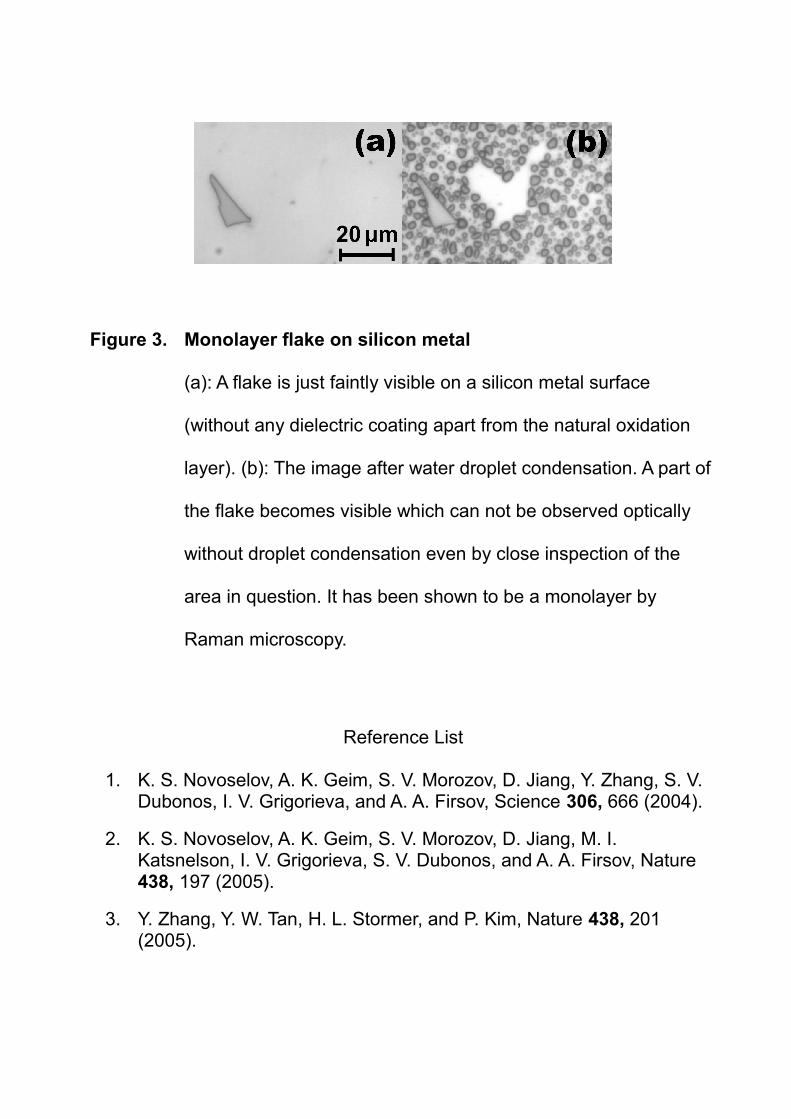
Figure 3. Monolayer flake on silicon metal
(a): A flake is just faintly visible on a silicon metal surface
(without any dielectric coating apart from the natural oxidation
layer). (b): The image after water droplet condensation. A part of
the flake becomes visible which can not be observed optically
without droplet condensation even by close inspection of the
area in question. It has been shown to be a monolayer by
Raman microscopy.
Reference List
1. K. S. Novoselov, A. K. Geim, S. V. Morozov, D. Jiang, Y. Zhang, S. V. Dubonos, I. V. Grigorieva, and A. A. Firsov, Science 306, 666 (2004).
2. K. S. Novoselov, A. K. Geim, S. V. Morozov, D. Jiang, M. I. Katsnelson, I. V. Grigorieva, S. V. Dubonos, and A. A. Firsov, Nature 438, 197 (2005).
3. Y. Zhang, Y. W. Tan, H. L. Stormer, and P. Kim, Nature 438, 201 (2005).
4. E. McCann and V. I. Fal'ko, Phys. Rev. Lett. 96, 086805 (2006).
5. A. Reina, X. T. Jia, J. Ho, D. Nezich, H. B. Son, V. Bulovic, M. S. Dresselhaus, and J. Kong, Nano Letters 9, 30 (2009).
6. A. H. Castro Neto, F. Guinea, N. M. R. Peres, K. S. Novoselov, and A. K. Geim, Rev. Mod. Phys. 81, 109 (2009).
7. A. K. Geim, Science 324, 1530 (2009).
8. J. Tworzydlo, B. Trauzettel, M. Titov, A. Rycerz, and C. W. J. Beenakker, Phys. Rev. Lett. 96, 246802 (2006).
9. C. Lee, X. D. Wei, J. W. Kysar, and J. Hone, Science 321, 385 (2008).
10. N. Stander, B. Huard, and D. Goldhaber-Gordon, Phys. Rev. Lett. 102, 026807 (2009).
11. P. Avouris, Z. H. Chen, and V. Perebeinos, Nature Nanotechnology 2, 605 (2007).
12. J. Kim, F. Kim, and J. X. Huang, Materials Today 13, 28 (2010).
13. D. S. L. Abergel, A. Russell, and V. I. Fal'ko, Appl. Phys. Lett. 91, 063125 (2007).
14. P. Blake, E. W. Hill, A. H. C. Neto, K. S. Novoselov, D. Jiang, R. Yang, T. J. Booth, and A. K. Geim, Appl. Phys. Lett. 91, 063124 (2007).
15. L. B. Gao, W. C. Ren, F. Li, and H. M. Cheng, Acs Nano 2, 1625 (2008).
16. K. S. Novoselov, D. Jiang, F. Schedin, T. J. Booth, V. V. Khotkevich, S. V. Morozov, and A. K. Geim, Proc. Natl. Acad. Sci. U. S. A. 102, 10451 (2005).
17. C. Casiraghi, A. Hartschuh, E. Lidorikis, H. Qian, H. Harutyunyan, T. Gokus, K. S. Novoselov, and A. C. Ferrari, Nano Letters 7, 2711 (2007).
18. D. Graf, F. Molitor, K. Ensslin, C. Stampfer, A. Jungen, C. Hierold, and L. Wirtz, Nano Letters 7, 238 (2007).
19. J. Kim, L. J. Cote, F. Kim, and J. X. Huang, J. Am. Chem. Soc. 132,
260 (2010).
20. I. Jung, M. Vaupel, M. Pelton, R. Piner, D. A. Dikin, S. Stankovich, J. An, and R. S. Ruoff, Journal of Physical Chemistry C 112, 8499 (2008).
21. R. R. Nair, P. Blake, A. N. Grigorenko, K. S. Novoselov, T. J. Booth, T. Stauber, N. M. R. Peres, and A. K. Geim, Science 320, 1308 (2008).
22. Y. Lee, S. Bae, H. Jang, S. Jang, S. E. Zhu, S. H. Sim, Y. I. Song, B. H. Hong, and J. H. Ahn, Nano Letters 10, 490 (2010).
23. X. S. Li, W. W. Cai, J. H. An, S. Kim, J. Nah, D. X. Yang, R. Piner, A. Velamakanni, I. Jung, E. Tutuc, S. K. Banerjee, L. Colombo, and R. S. Ruoff, Science 324, 1312 (2009).
24. Lord Rayleigh, Nature 90, 436 (1913).
25. G. T. Carroll, D. N. Wang, N. J. Turro, and J. T. Koberstein, Langmuir 22, 2899 (2006).
26. C. D. Frisbie, L. F. Rozsnyai, A. Noy, M. S. Wrighton, and C. M. Lieber, Science 265, 2071 (1994).
27. R. Hofer, M. Textor, and N. D. Spencer, Langmuir 17, 4123 (2001).
28. G. P. Lopez, H. A. Biebuyck, C. D. Frisbie, and G. M. Whitesides, Science 260, 647 (1993).
29. J. Aizenberg, A. J. Black, and G. M. Whitesides, Nature 394, 868 (1998).
30. Y. M. Zheng, D. Han, J. Zhai, and L. Jiang, Appl. Phys. Lett. 92, 084106 (2008).
31. E. Bonaccurso, H. J. Butt, and K. Graf, Eur. Polym. J. 40, 975 (2004).
32. C. Schafle, P. Leiderer, and C. Bechinger, Europhys. Lett. 63, 394 (2003).