Embed Size (px)
Citation preview

eScholarship provides open access, scholarly publishingservices to the University of California and delivers a dynamicresearch platform to scholars worldwide.
University of California
Peer Reviewed
Title:Emerging memory devices - Nontraditional possibilities based on nanomaterials andnanostructures
Author:Galatsis, KWang, KBotros, YYang, YXie, Y HStoddart, J FKaner, Richard B, University of California, Los AngelesOzkan, CLiu, J LOzkan, MZhou, C WKim, K W
Publication Date:05-01-2006
Publication Info:Postprints, UC Los Angeles
Permalink:http://escholarship.org/uc/item/1343s647
Additional Info:©2006 IEEE. Personal use of this material is permitted. However, permission to reprint/republishthis material for advertising or promotional purposes or for creating new collective works for resaleor redistribution to servers or lists, or to reuse any copyrighted component of this work in otherworks must be obtained from the IEEE.
With MP3 player capacity at more than 60 GB,digital camera memory surpassing 1 GB, andstandard personal computers boasting over 1GB random access memory (RAM), the old
Commodore 64s (64 KB RAM) and 3 1/2-in floppy drives (1.44MB) make us wonder how did we ever survive? New memorytechnologies such as FLASH have had a huge impact on con-sumers, as have traditional static RAMs (SRAM) and dynamicRAMs (DRAM). But the main culprit of the continual techno-logical revolution is by far scaling.
SRAM stores data in flip-flops that are made up of four tosix transistors. SRAM is fast and does not require frequentrefreshing, but it does take up valuable Si real estate. It is con-sidered the fastest RAM available and is usually employed asan on-chip cache. DRAM, on the other hand, is made up ofone transistor and one capacitor but requires refreshing tomaintain capacitor charge. Fewer elements mean more mem-ory per unit chip area. Today’s popular breed of DRAM, knownas synchronous DRAM (SDRAM), is found in most computersystems as primary memory storage. SDRAM can run at muchhigher clock speeds than conventional memory as it synchro-
nizes itself with the CPU’s bus. The DRAM market in 2004 wasworth over US$26.8 billion, coming close to the lucrativemicroprocessor market at US$30.5 billion. Catching up fast,at a market value of US$15.6 billion in 2004, is the popularFLASH (NAND)-based memory, aggressively dominating thememory market in growth. Toshiba Corp. developed the firstNAND FLASH as a solid-state replacement for magnetic mem-ory. FLASH is made up of one transistor with a specially engi-neered floating gate that maintains charge states. The FLASHrevolution has enabled consumers to enjoy the pleasures ofportable MP3 players and digital cameras with abundant stor-age. Growth in each memory sector is expected to increasewell into 2008. The International Technology Roadmap forSemiconductors (ITRS) and the Semiconductor Research Cor-poration (SRC) Memory Task Force reports such growth ratescannot be sustained due to scaling issues.
Exotic solutions such as three-dimensional integration,stacking [1], distributed memory, processor in memory (PIM),memory in processor (MIP) [2], [3], and other new architec-tures being reported in the literature may somewhat sustainMoore’s law for memory beyond 2008 based on existing
Kosmas Galatsis, Kang Wang,Youssry Botros,
Yang Yang, Ya-Hong Xie,J.F. Stoddart, R.B. Kaner,
Cengiz Ozkan, Jianlin Liu,Mihri Ozkan, Chongwu Zhou,
and Ki Wook Kim
■ 12 IEEE CIRCUITS & DEVICES MAGAZINE ■ MAY/JUNE 20068755-3996/06/$20.00 ©2006 IEEE
Nontraditional Possibilities Based on Nanomaterials and Nanostructures
memory devices. To make trueleaps in sustaining memorygrowth, industry and academiaare searching for new and novelmemory devices. Numerousemerging memory devicesbased on nanomaterials andnanostructures have been wellidentified by the ITRS [4], the SRC Memory Task Force [5],and the European Roadmap for Nanoelectronics [6]. In aneffort to collate possible memory device alternatives, the ITRSRoadmap identifies six emerging research memory areasbeyond traditional RAM and FLASH devices. These includephase change memory, floating body DRAM, nano floatinggate memory, single electron memory, insulator resistancechange memory, and molecular memory, which are also posi-tively reviewed in [7]. In addition, there have been variousreview papers [8]–[15] comparing and investigating alternativememory devices that include ferroelectric RAM, magneticRAM, organic RAM, CNT electromechanical nonvolatile mem-ory, programmable metallization cell (PMC) memory, magnet-ic tunneling junctions (MTJ) RAM, and thyristor RAM.
Each memory type provides its unique advantages andchallenges. However, for the “next” memory device to be con-sidered as a silver bullet solution it would need to possess thefollowing attributes: 1) fast access time, 2) nonvolatility, 3)infinite read/write cycles, 4) low power, and 5) a wide operat-ing temperature range. From a manufacturing perspective,additional attributes are also required such as 6) scalability, 7)low cost, 8) manufacturability, 9) variability (of nanodevicefeature size), and 10) integration ability with the Si platform.At this time, the silver bullet solution to this wish list is stillunknown. As we delve further into the nanoregime, we arepresented with ever-increasing material options, processes,
and fascinating mechanismsnever before made possible.
In an attempt to merge theunprecedented opportunity ofnanotechnology with theindustry’s imminent scalingand power dissipation chal-lenges, the Center on Func-
tional Engineered Nano Architectonics (FENA), sponsored bythe Semiconductor Industry Association (SIA), Semiconduc-tor Equipment and Materials International (SEMI), and theDepartment of Defense (managed by DARPA), aims to engi-neer nontraditional memory alternatives based on nanomate-rials and structures that may go beyond existing CMOSmemory devices. Nanomaterial engineering provides opportu-nities that have never before been possible such as the abilityto self-assemble, develop controlled composite nanomaterials,and manipulate alternative state variables. Such attributesshould also translate into simplified production with dramati-cally reduced costs. This article will provide a taste of theexotic and nontraditional memory possibilities that haveemerged from the FENA Center.
EMERGING MEMORY DEVICESThe list of emerging memory devices and concepts based onnovel nanomaterials and nanostructures developed by FENAis presented in Table 1. The table includes memory conceptsthat are the outcomes of FENA’s devices, nanomaterials,nanostructures, and computational research. We present thenew memory devices together with data on current devicessuch as DRAM, which represents the largest volatile memorymarket, and FLASH, which represents the largest solid-statenonvolatile memory market. The table presents both demon-strated values (in bold and brackets) and projected parameter
13 ■IEEE CIRCUITS & DEVICES MAGAZINE ■ MAY/JUNE 2006
SRAM is fast and does not requirefrequent refreshing, but it does take
up valuable Si real estate.
PH
OT
O C
RE
DIT
©D
AR
RE
N K
EO
GH

■ 14 IEEE CIRCUITS & DEVICES MAGAZINE ■ MAY/JUNE 2006
Mol
ecul
er –B
ased
Mem
orie
s
Rota
xane
Mem
ory
Polym
er M
emor
ySt
orag
ePr
esen
t-D
ay B
asel
ine
Tech
nolo
gies
(F. S
todd
art
and
Viru
s M
emor
yN
anow
ire M
emor
y(R
. Kan
eran
d Y.
Yan
g)Si
ngle
Ele
ctro
nPh
ase-
Char
geSp
in M
emor
yM
echa
nism
(Tak
en fr
om IT
RS 2
005
Editi
on)
W. G
odda
rd( Y
. Yan
g an
d C.
Ozk
an)
(C. Z
hou)
Mem
ory
(J. L
iu)
RAM
(Y.H
. Xie
)(K
.W. K
im)
Dev
ice
Type
, St
anda
lone
N
OR
Flas
h-(2
005)
Rota
xane
s or
Pr
otei
n Vi
rus
Nan
owire
s;
Polya
nilin
eFl
oatin
g Ga
te
GeSb
TeSp
in S
tate
M
ater
ial U
sed
DR
AM (2
005)
130-
nm n
ode
Cate
nane
s N
anow
ires w
ith
In20 3
, Si w
ith
Nan
owire
s U
sing
CoS
i 2/S
i Te
mpl
ated
Sel
f-Va
riabl
e Usi
ng80
- nm
nod
e Pl
atin
um
Redo
x Ac
tive
with
Au
Het
ero-
Asse
mbl
ed P
S-H
igh
Tem
p N
anop
artic
les
Mol
ecul
esN
anop
artic
les
Nan
ocry
stal
s PI
Blo
ck C
opol
y.D
MS
Read
Tim
e (<<<
15 n
s)(1
4 ns
) ∼ n
s —
<
80 n
s ∼ 2
5 ns
<
80 n
s <
50 n
s <
80 n
s
Writ
e Ti
me
(<<<15
ns)
(1
µµµS)
∼µ
S ∼ 1
µs
(~25
ns)
∼ 2
5 ns
(∼∼∼
0.4
µµµS)
<50
ns
∼ 1 n
s
Rete
ntio
n Ti
me
(64
ms)
>
10 y
ears
(m
inut
es)
(day
s)
(600
hou
rs)
(wee
ks)
10–2
0 ye
ars
>1 0
yea
rs
>ye
ars
Writ
e Cy
cles
In
finite
(>>>
100,
000)
∼ 1
00 (<
35)
∼ 1,0
00
(∼∼∼1,
000)
(>
10,0
00)
>1O
O,0
00
>1
billio
n >
100,
000
On/
Off
<10
,000
∼ 1
0,00
0 >
100
Unk
now
nRa
tio(<<<
10,0
00)
(<<<10
,000
) (∼
2 −
11)
(∼10
00)
(∼∼∼10
,000
)(∼∼∼
1000
)[a
]Sc
alab
ility
32 n
m N
ode
45 n
m N
ode
(0.0
07 µµµ
m2
)(0
.01
µµµm
2)
<0.
0001
µm
2(0
.04
µµµm
2)
(1 µµµ
m2
)∼ 0
.04
µm
2<
O.Q
001
µm
2
ceil
size
in µ
m2
6F2
�0.
0061
IO
F2�
O.0
21<
0.00
01 µ
m2
<0.
0001
µm
2<
0.00
01 µ
m2
<0.
0011
µm
2
Lim
iting
Sca
ling
Hig
h-k
Mat
eria
lO
xide
Thi
ckne
ss
Mol
ecul
e Va
riabi
lity
of
Mol
ecul
e
Varia
bilit
y of
D
ot D
ensi
ty
Den
sity
Lim
ited
Curie
Tem
pFa
ctor
Stab
ility
and
Self-
M
etal
Par
ticle
St
abilit
y an
d Se
lf-M
etal
Par
ticle
Fluc
tuat
ion
by T
herm
al
of D
MS
Asse
mbl
y Si
ze a
nd D
ensi
ty
Asse
mbl
y Si
ze a
nd D
ensi
ty
Prox
imity
Va
riabi
lity
Varia
bilit
yEf
fect
Gene
ral
Hig
h D
ensi
ty,
Non
vola
tile
Ultr
a H
igh
Den
sity
Low
Cos
t, H
igh
Low
Cos
t, F
lexi
ble,
Low
Cos
t, H
igh
Hig
h D
ensi
ty,
Non
vola
tile,
Hig
h D
ensi
ty,
Adva
ntag
es
Econ
omic
al
Den
sity
, Bio
H
igh
Den
sity
D
ensi
ty, F
ast
CMO
S St
able
, Lo
w P
ower
,Co
mpa
tible
Co
mpa
tible
Scal
able
Sc
alab
le
Chal
leng
es
Scal
ing,
Gat
e Sc
alin
g, O
xide
Sp
eed,
Sta
bilit
y,M
ater
ial S
tabi
lity
Inte
grat
ion
and
Mat
eria
l Sta
bilit
y,D
ot D
ensi
ty
Larg
e W
rite
Curr
ent,
M
ater
ial,
Hig
h Le
akag
e,
Thic
knes
s, P
ower
O
n/O
ff Ra
tio,
Inte
grat
ion,
M
ater
ial S
tabi
lity
Inte
grat
ion,
Fl
uctu
atio
n,
New
Mat
eria
ls
Curie
Tem
pCa
paci
tor
Dis
sipa
tion
Tem
p In
fluen
ce
Scal
ing
Tem
p In
fluen
ce
Scal
ing
and
Proc
ess
Form
atio
n
Fabr
icat
ion
Lith
ogra
phy
Lith
ogra
phy
Lith
o an
d Se
lf-Se
lf-As
sem
bly,
Lith
o an
d Se
lf–As
sem
bly,
Li
tho
and
Polym
er T
empl
ate
Lith
o Te
chni
que
Asse
mbl
y W
et S
ynth
esis
Self-
Asse
mbl
y W
et S
ynth
esis
Se
lf-As
sem
bly
and
Lith
o
[a] C
ell S
ize =
αF
2, w
here
αis
the
cel
l size
fact
or a
nd F
is t
he h
alf p
itch
node
. DRA
M c
ell s
ize is
8 F
2an
d 10
F2
for
NO
R Fl
ash.
The
nod
es a
nd y
ears
(DRA
M –
yea
r 20
13, N
OR
Flas
h –
2010
) wer
e se
lect
ed a
s th
e fir
st “r
edbr
icks
” app
ear
indi
catin
g m
anuf
actu
ring
solu
tions
are
pre
sent
ly N
OT
know
n (IT
RS
2005
Edi
tion,
Pro
cess
Inte
grat
ion
Dev
ices
and
Str
uctu
res
Sect
ion,
pp.
31
and
34).
Tabl
e 1.
Pro
ject
ed/e
xper
imen
tal p
aram
eter
s of
FEN
A em
ergi
ng r
esea
rch
mem
ory
devi
ces.
values (normal). Advantagesand key challenges are alsohighlighted together with thecorresponding fabricationmethods. Each type of memorywill be described.
MOLECULAR MEMORYThe ITRS [4] has identifiedmolecular-based memory as an emerging technology, utiliz-ing molecular-level components, which promises the ulti-mate dimensional limit for memory. Integration of thecomponents into memory devices typically involves molecu-lar assembly, rather than patterning two-dimensional semi-conductor surfaces with doped regions. Hence, molecularelectronics rely on assembly from the bottom up.
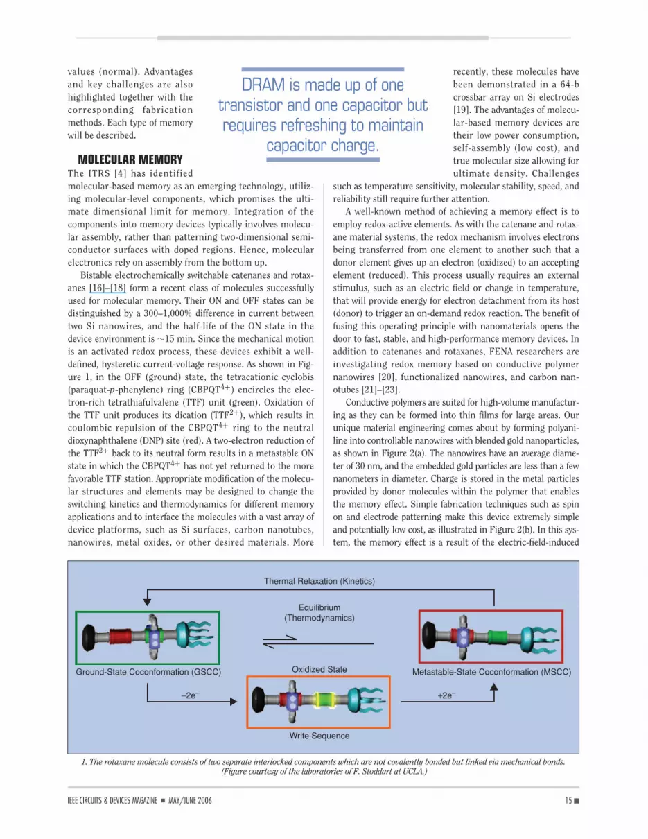
Bistable electrochemically switchable catenanes and rotax-anes [16]–[18] form a recent class of molecules successfullyused for molecular memory. Their ON and OFF states can bedistinguished by a 300–1,000% difference in current betweentwo Si nanowires, and the half-life of the ON state in thedevice environment is ∼15 min. Since the mechanical motionis an activated redox process, these devices exhibit a well-defined, hysteretic current-voltage response. As shown in Fig-ure 1, in the OFF (ground) state, the tetracationic cyclobis(paraquat-p-phenylene) ring (CBPQT4+) encircles the elec-tron-rich tetrathiafulvalene (TTF) unit (green). Oxidation ofthe TTF unit produces its dication (TTF2+), which results incoulombic repulsion of the CBPQT4+ ring to the neutraldioxynaphthalene (DNP) site (red). A two-electron reduction ofthe TTF2+ back to its neutral form results in a metastable ONstate in which the CBPQT4+ has not yet returned to the morefavorable TTF station. Appropriate modification of the molecu-lar structures and elements may be designed to change theswitching kinetics and thermodynamics for different memoryapplications and to interface the molecules with a vast array ofdevice platforms, such as Si surfaces, carbon nanotubes,nanowires, metal oxides, or other desired materials. More
recently, these molecules havebeen demonstrated in a 64-bcrossbar array on Si electrodes[19]. The advantages of molecu-lar-based memory devices aretheir low power consumption,self-assembly (low cost), andtrue molecular size allowing forultimate density. Challenges
such as temperature sensitivity, molecular stability, speed, andreliability still require further attention.
A well-known method of achieving a memory effect is toemploy redox-active elements. As with the catenane and rotax-ane material systems, the redox mechanism involves electronsbeing transferred from one element to another such that adonor element gives up an electron (oxidized) to an acceptingelement (reduced). This process usually requires an externalstimulus, such as an electric field or change in temperature,that will provide energy for electron detachment from its host(donor) to trigger an on-demand redox reaction. The benefit offusing this operating principle with nanomaterials opens thedoor to fast, stable, and high-performance memory devices. Inaddition to catenanes and rotaxanes, FENA researchers areinvestigating redox memory based on conductive polymernanowires [20], functionalized nanowires, and carbon nan-otubes [21]–[23].
Conductive polymers are suited for high-volume manufactur-ing as they can be formed into thin films for large areas. Ourunique material engineering comes about by forming polyani-line into controllable nanowires with blended gold nanoparticles,as shown in Figure 2(a). The nanowires have an average diame-ter of 30 nm, and the embedded gold particles are less than a fewnanometers in diameter. Charge is stored in the metal particlesprovided by donor molecules within the polymer that enablesthe memory effect. Simple fabrication techniques such as spinon and electrode patterning make this device extremely simpleand potentially low cost, as illustrated in Figure 2(b). In this sys-tem, the memory effect is a result of the electric-field-induced
15 ■IEEE CIRCUITS & DEVICES MAGAZINE ■ MAY/JUNE 2006
1. The rotaxane molecule consists of two separate interlocked components which are not covalently bonded but linked via mechanical bonds.(Figure courtesy of the laboratories of F. Stoddart at UCLA.)
Write Sequence
Oxidized State
Equilibrium(Thermodynamics)
Ground-State Coconformation (GSCC) Metastable-State Coconformation (MSCC)
Thermal Relaxation (Kinetics)
−2e− +2e−
DRAM is made up of onetransistor and one capacitor butrequires refreshing to maintain
capacitor charge.
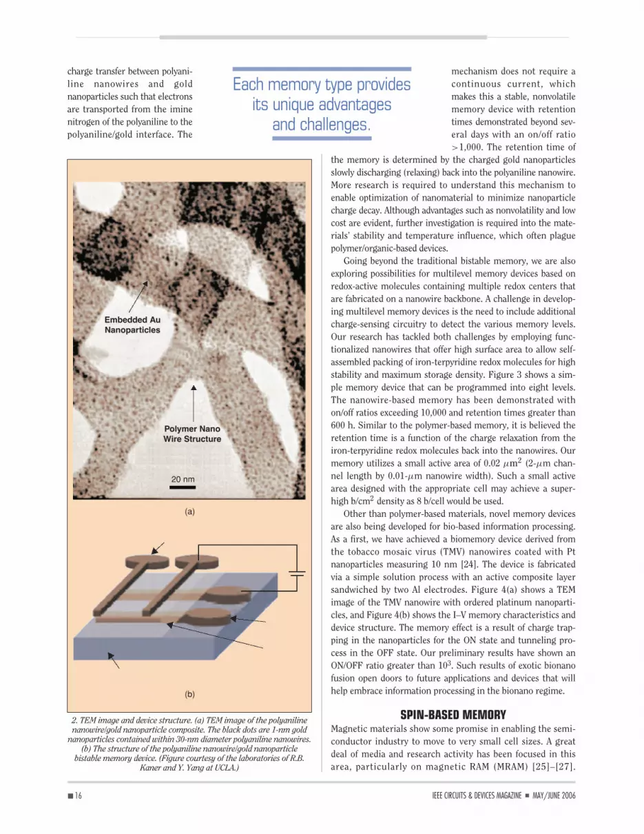
charge transfer between polyani-line nanowires and goldnanoparticles such that electronsare transported from the iminenitrogen of the polyaniline to thepolyaniline/gold interface. The
mechanism does not require acontinuous current, whichmakes this a stable, nonvolatilememory device with retentiontimes demonstrated beyond sev-eral days with an on/off ratio>1,000. The retention time of
the memory is determined by the charged gold nanoparticlesslowly discharging (relaxing) back into the polyaniline nanowire.More research is required to understand this mechanism toenable optimization of nanomaterial to minimize nanoparticlecharge decay. Although advantages such as nonvolatility and lowcost are evident, further investigation is required into the mate-rials’ stability and temperature influence, which often plaguepolymer/organic-based devices.
Going beyond the traditional bistable memory, we are alsoexploring possibilities for multilevel memory devices based onredox-active molecules containing multiple redox centers thatare fabricated on a nanowire backbone. A challenge in develop-ing multilevel memory devices is the need to include additionalcharge-sensing circuitry to detect the various memory levels.Our research has tackled both challenges by employing func-tionalized nanowires that offer high surface area to allow self-assembled packing of iron-terpyridine redox molecules for highstability and maximum storage density. Figure 3 shows a sim-ple memory device that can be programmed into eight levels.The nanowire-based memory has been demonstrated withon/off ratios exceeding 10,000 and retention times greater than600 h. Similar to the polymer-based memory, it is believed theretention time is a function of the charge relaxation from theiron-terpyridine redox molecules back into the nanowires. Ourmemory utilizes a small active area of 0.02 µm2 (2-µm chan-nel length by 0.01-µm nanowire width). Such a small activearea designed with the appropriate cell may achieve a super-high b/cm2 density as 8 b/cell would be used.
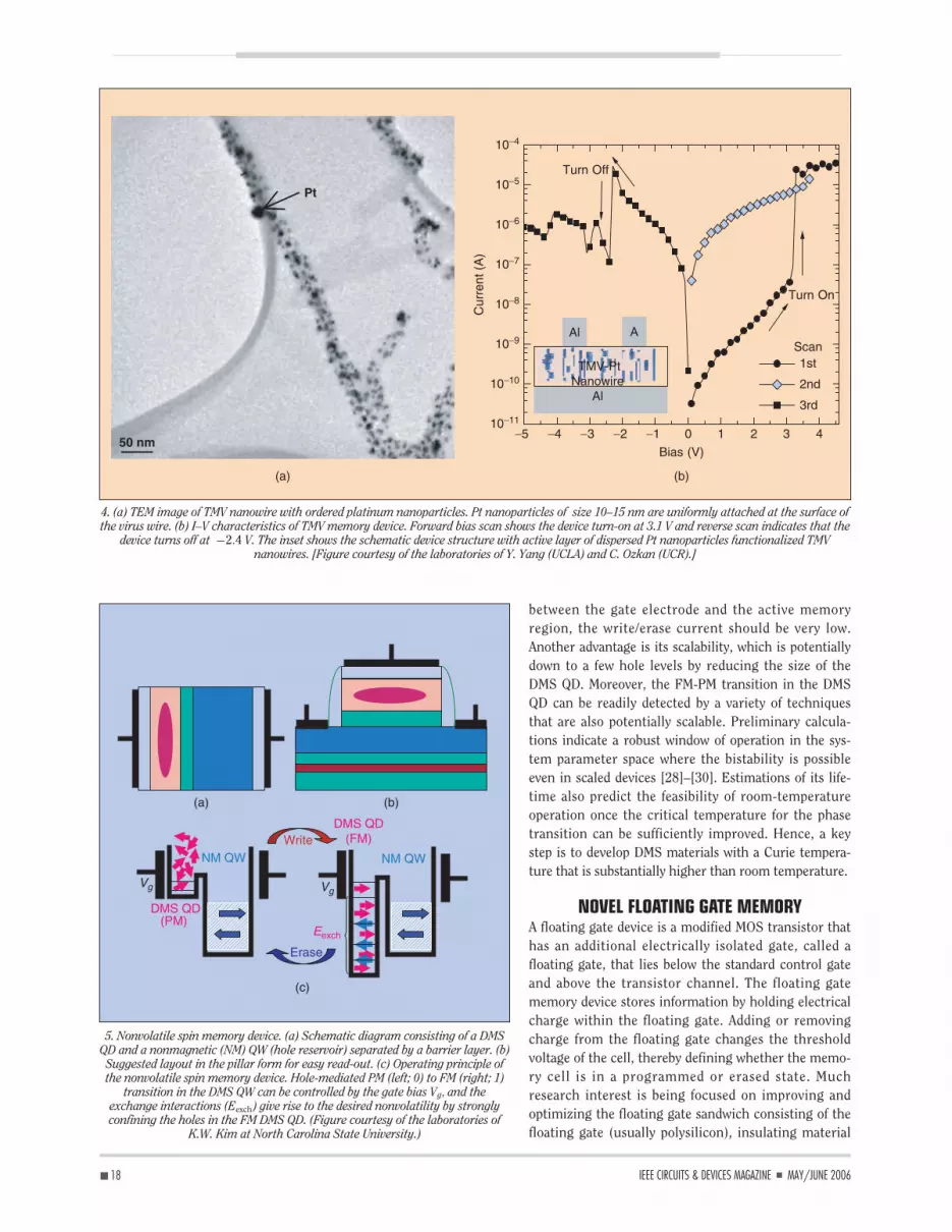
Other than polymer-based materials, novel memory devicesare also being developed for bio-based information processing.As a first, we have achieved a biomemory device derived fromthe tobacco mosaic virus (TMV) nanowires coated with Ptnanoparticles measuring 10 nm [24]. The device is fabricatedvia a simple solution process with an active composite layersandwiched by two Al electrodes. Figure 4(a) shows a TEMimage of the TMV nanowire with ordered platinum nanoparti-cles, and Figure 4(b) shows the I–V memory characteristics anddevice structure. The memory effect is a result of charge trap-ping in the nanoparticles for the ON state and tunneling pro-cess in the OFF state. Our preliminary results have shown anON/OFF ratio greater than 103. Such results of exotic bionanofusion open doors to future applications and devices that willhelp embrace information processing in the bionano regime.
SPIN-BASED MEMORYMagnetic materials show some promise in enabling the semi-conductor industry to move to very small cell sizes. A greatdeal of media and research activity has been focused in thisarea, particularly on magnetic RAM (MRAM) [25]–[27].
■ 16 IEEE CIRCUITS & DEVICES MAGAZINE ■ MAY/JUNE 2006
2. TEM image and device structure. (a) TEM image of the polyanilinenanowire/gold nanoparticle composite. The black dots are 1-nm gold
nanoparticles contained within 30-nm diameter polyaniline nanowires.(b) The structure of the polyaniline nanowire/gold nanoparticle
bistable memory device. (Figure courtesy of the laboratories of R.B.Kaner and Y. Yang at UCLA.)
Polymer NanoWire Structure
Embedded AuNanoparticles
20 nm
(a)
(b)
Each memory type providesits unique advantages
and challenges.

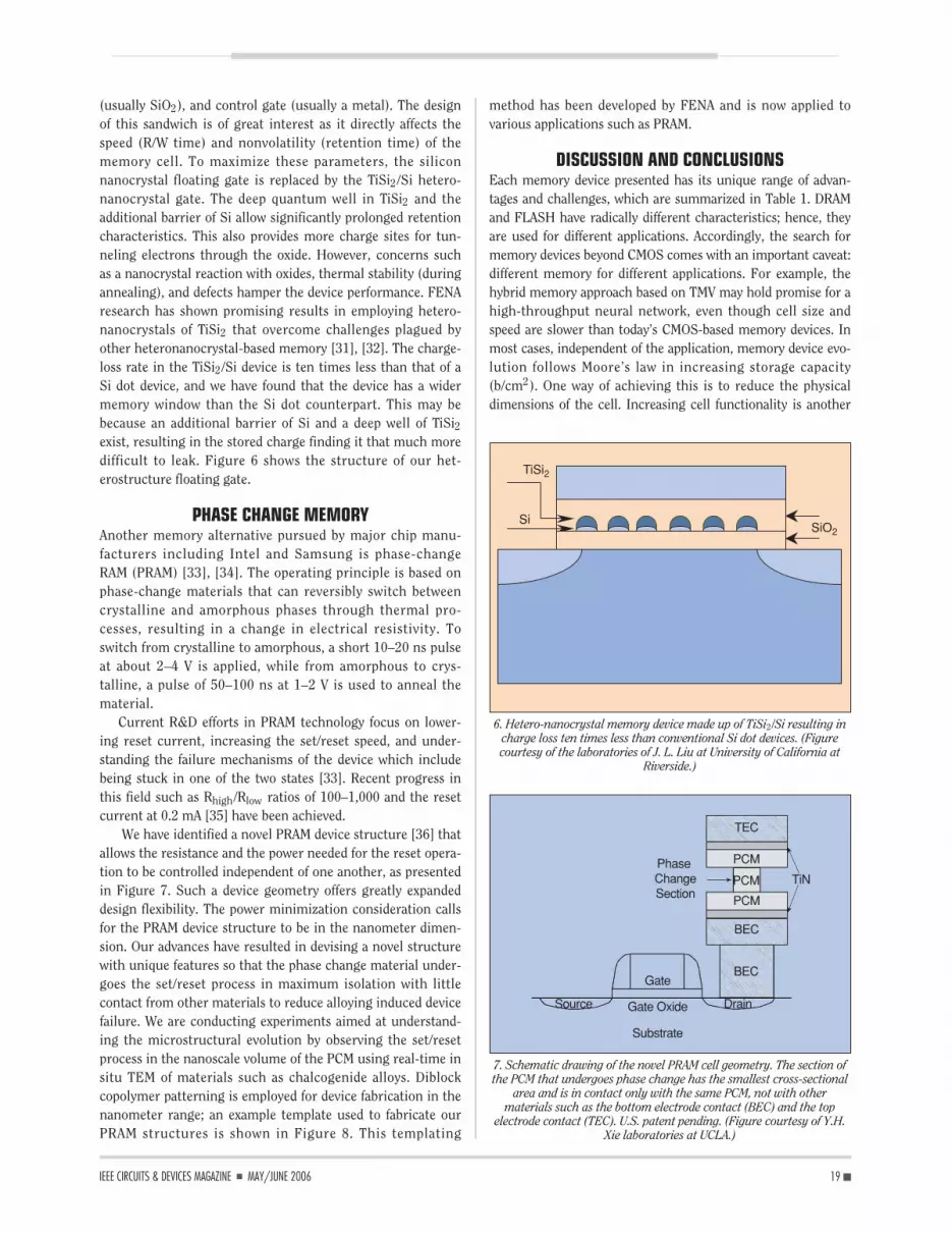
Spintronics enable informationrepresentation to be based onangular spin momentumrather than electron charge. Itis hoped that by employingspin as a state variable, powerdissipation could be dramati-cally reduced. The challengerests in developing a spin-based memory cell that can beintegrated on a Si substrate. Dilute magnetic semiconduc-tors (DMSs) provide a path to such an ambitious task. Oneinteresting spin memory device proposed [28]–[30] is thebistable double-quantum well structure mediated by a mag-netic phase transition as presented in Figure 5. A gate elec-trode is also needed to control the hole transfer between thequantum device (QD) and the reservoir.
The basic operating princi-ple is as follows: The DMS QDcan be prepared initially in aparamagnetic (PM) state bydepopulating holes throughproper bandgap engineeringwith the neighboring reservoirand barriers. When a proper
bias is applied to the gate electrode, holes from the reservoircan be transferred to the DMS QD via tunneling or overbarrierinjection. As the hole density in the DMS QD surpasses a cer-tain threshold, the layer undergoes a PM to ferromagnetic (FM)transition, thus writing the spin memory. When a reverse biaspulse is applied, the holes are drained out of the FM DMS QDinto the reservoir and the DMS will return to the PM state,thus erasing the spin memory. Owing to the insulating barrier
17 ■IEEE CIRCUITS & DEVICES MAGAZINE ■ MAY/JUNE 2006
3. Schematic diagram compares design and operation for a conventional silicon FLASH memory and the proposed molecular memory formultilevel nonvolatile data storage. (a) Schematic of a silicon FLASH memory, (b) schematic of the proposed molecular memory, and (c) I-Vg
hysteresis loops obtained by sweeping gate voltage from −n ∗ 2.5 V to 10 + n ∗ 2.5 V and then back to the starting value. n is the index of levelsfrom 2 (the innermost curve) to 8 (the outermost curve). (d) Current recorded over time after the device was written into states 0 (the bottomcurve) to 8 (the top curve). Little degradation in the stored signal was observed over 1,500 s with a source-drain bias of V = −0.1 V. (Figure
courtesy of the laboratories of C. Zhou at USC.)
−1,600
−1,200
−800
−400
0
I (nA
)
3020100−10−20Vg (V)
−1,400
−1,200
−1,000
−800
−600
−400
−200
0
I (nA
)
1,6001,200800400Time (s)
(c) (d)
“8“7
“6
“5
“4
“0
“3
“2“1
V = −0.1
Control Gate
Oxide
Floating Gate
P-Type Substrate
Lightly n-Doped
Heavily n-Doped
Silicon Memory
Control Gate
Oxide
Metal
Nanowire
Redox Molecule Molecular Memory
(a)
(b)
The ITRS has identified molecular-based memory
as an emerging technology.
between the gate electrode and the active memoryregion, the write/erase current should be very low.Another advantage is its scalability, which is potentiallydown to a few hole levels by reducing the size of theDMS QD. Moreover, the FM-PM transition in the DMSQD can be readily detected by a variety of techniquesthat are also potentially scalable. Preliminary calcula-tions indicate a robust window of operation in the sys-tem parameter space where the bistability is possibleeven in scaled devices [28]–[30]. Estimations of its life-time also predict the feasibility of room-temperatureoperation once the critical temperature for the phasetransition can be sufficiently improved. Hence, a keystep is to develop DMS materials with a Curie tempera-ture that is substantially higher than room temperature.
NOVEL FLOATING GATE MEMORYA floating gate device is a modified MOS transistor thathas an additional electrically isolated gate, called afloating gate, that lies below the standard control gateand above the transistor channel. The floating gatememory device stores information by holding electricalcharge within the floating gate. Adding or removingcharge from the floating gate changes the thresholdvoltage of the cell, thereby defining whether the memo-ry cell is in a programmed or erased state. Muchresearch interest is being focused on improving andoptimizing the floating gate sandwich consisting of thefloating gate (usually polysilicon), insulating material
■ 18 IEEE CIRCUITS & DEVICES MAGAZINE ■ MAY/JUNE 2006
5. Nonvolatile spin memory device. (a) Schematic diagram consisting of a DMSQD and a nonmagnetic (NM) QW (hole reservoir) separated by a barrier layer. (b)Suggested layout in the pillar form for easy read-out. (c) Operating principle ofthe nonvolatile spin memory device. Hole-mediated PM (left; 0) to FM (right; 1)
transition in the DMS QW can be controlled by the gate bias Vg, and theexchange interactions (Eexch) give rise to the desired nonvolatility by stronglyconfining the holes in the FM DMS QD. (Figure courtesy of the laboratories of
K.W. Kim at North Carolina State University.)
(c)
Write
Erase
Vg
DMS QD(PM)
NM QW NM QW
DMS QD(FM)
Eexch
(a) (b)
Vg
4. (a) TEM image of TMV nanowire with ordered platinum nanoparticles. Pt nanoparticles of size 10–15 nm are uniformly attached at the surface ofthe virus wire. (b) I–V characteristics of TMV memory device. Forward bias scan shows the device turn-on at 3.1 V and reverse scan indicates that the
device turns off at −2.4 V. The inset shows the schematic device structure with active layer of dispersed Pt nanoparticles functionalized TMVnanowires. [Figure courtesy of the laboratories of Y. Yang (UCLA) and C. Ozkan (UCR).]
Al A
−5 −4 −3 −2 −1 0 1 2 3 410−11
10−10
10−9
10−8
10−7
10−6
10−5
10−4
Scan
1st
2nd
3rd
Cur
rent
(A
)
Bias (V)
Turn On
Turn Off
TMV-PtNanowire
Al
Pt
50 nm
(a) (b)
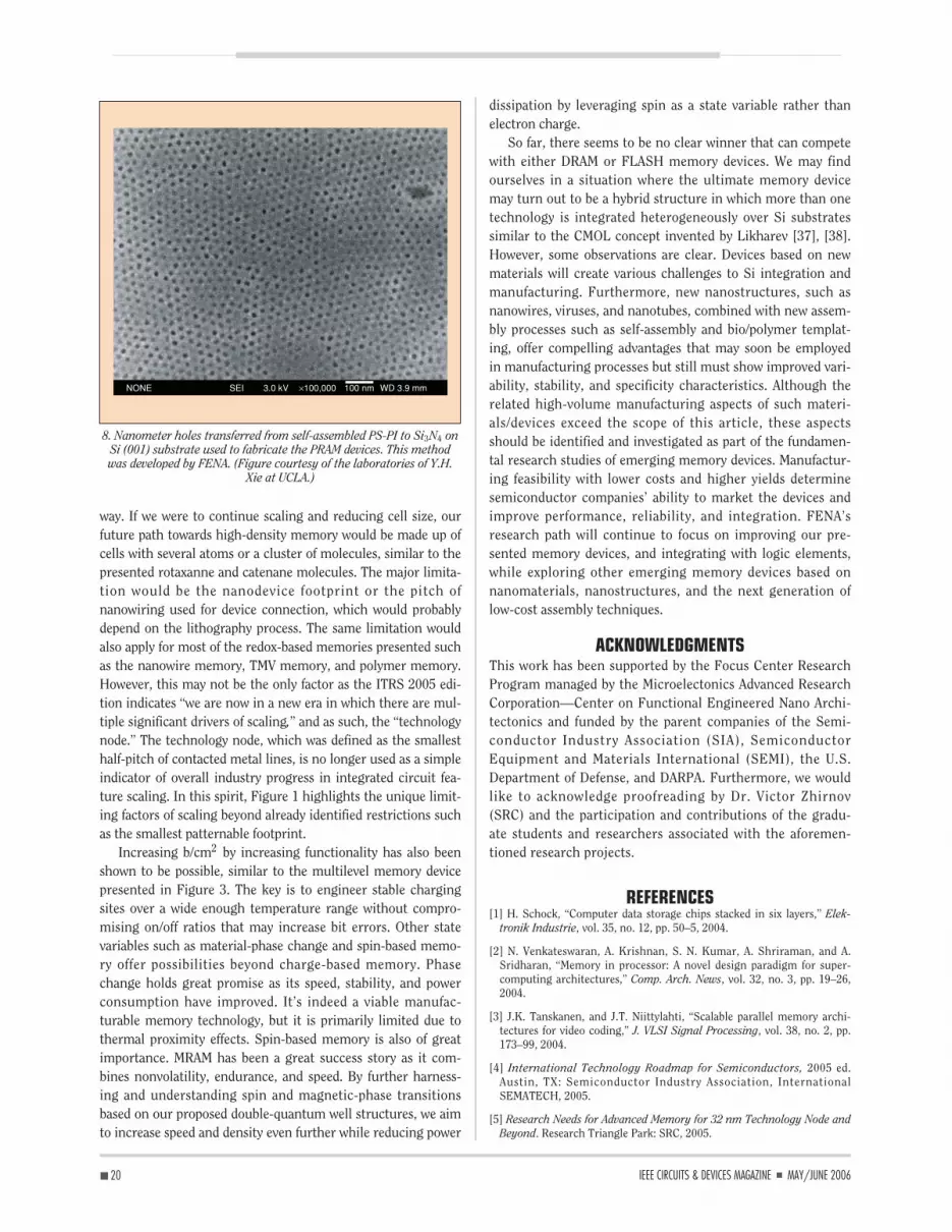
(usually SiO2), and control gate (usually a metal). The designof this sandwich is of great interest as it directly affects thespeed (R/W time) and nonvolatility (retention time) of thememory cell. To maximize these parameters, the siliconnanocrystal floating gate is replaced by the TiSi2/Si hetero-nanocrystal gate. The deep quantum well in TiSi2 and theadditional barrier of Si allow significantly prolonged retentioncharacteristics. This also provides more charge sites for tun-neling electrons through the oxide. However, concerns suchas a nanocrystal reaction with oxides, thermal stability (duringannealing), and defects hamper the device performance. FENAresearch has shown promising results in employing hetero-nanocrystals of TiSi2 that overcome challenges plagued byother heteronanocrystal-based memory [31], [32]. The charge-loss rate in the TiSi2/Si device is ten times less than that of aSi dot device, and we have found that the device has a widermemory window than the Si dot counterpart. This may bebecause an additional barrier of Si and a deep well of TiSi2exist, resulting in the stored charge finding it that much moredifficult to leak. Figure 6 shows the structure of our het-erostructure floating gate.
PHASE CHANGE MEMORYAnother memory alternative pursued by major chip manu-facturers including Intel and Samsung is phase-changeRAM (PRAM) [33], [34]. The operating principle is based onphase-change materials that can reversibly switch betweencrystalline and amorphous phases through thermal pro-cesses, resulting in a change in electrical resistivity. Toswitch from crystalline to amorphous, a short 10–20 ns pulseat about 2–4 V is applied, while from amorphous to crys-talline, a pulse of 50–100 ns at 1–2 V is used to anneal thematerial.
Current R&D efforts in PRAM technology focus on lower-ing reset current, increasing the set/reset speed, and under-standing the failure mechanisms of the device which includebeing stuck in one of the two states [33]. Recent progress inthis field such as Rhigh/Rlow ratios of 100–1,000 and the resetcurrent at 0.2 mA [35] have been achieved.
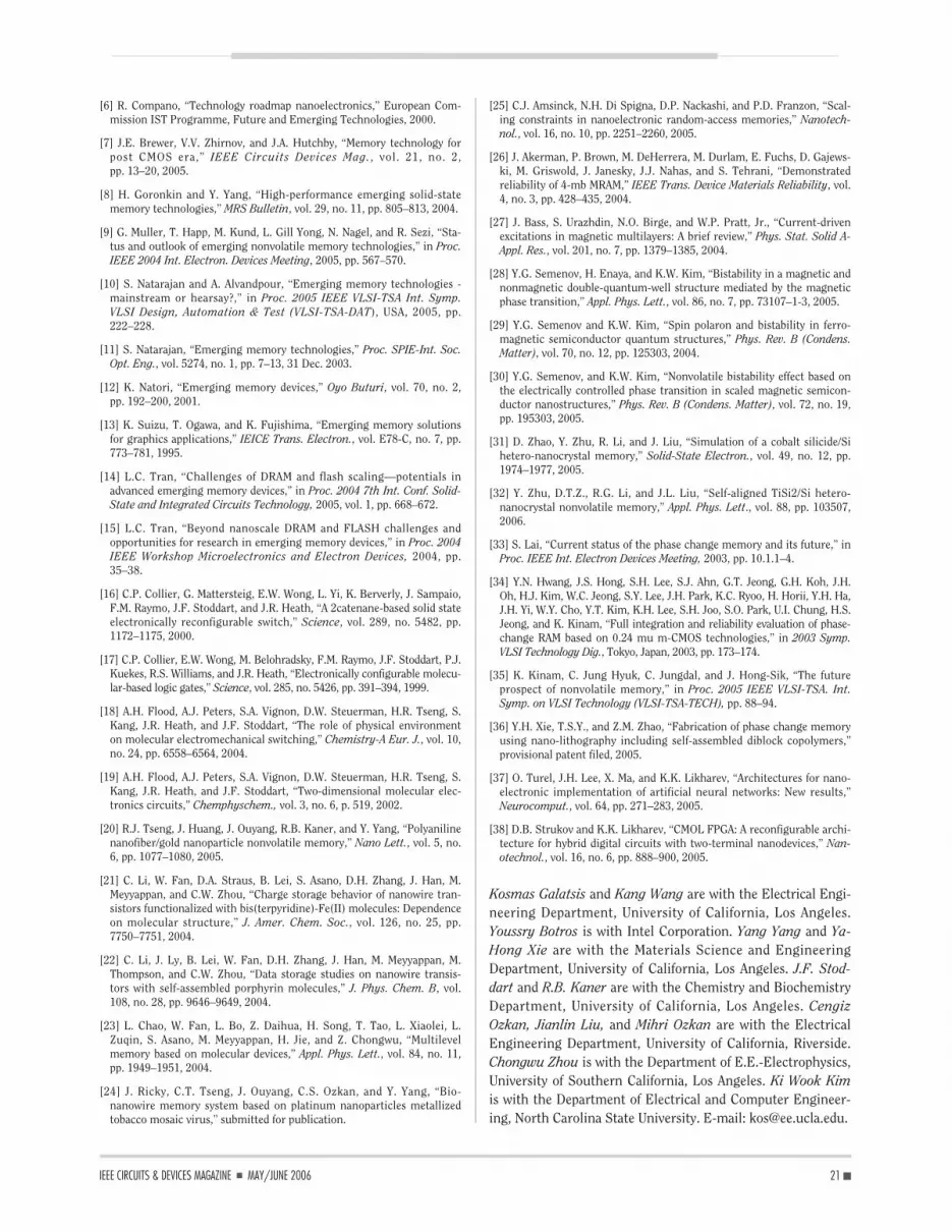
We have identified a novel PRAM device structure [36] thatallows the resistance and the power needed for the reset opera-tion to be controlled independent of one another, as presentedin Figure 7. Such a device geometry offers greatly expandeddesign flexibility. The power minimization consideration callsfor the PRAM device structure to be in the nanometer dimen-sion. Our advances have resulted in devising a novel structurewith unique features so that the phase change material under-goes the set/reset process in maximum isolation with littlecontact from other materials to reduce alloying induced devicefailure. We are conducting experiments aimed at understand-ing the microstructural evolution by observing the set/resetprocess in the nanoscale volume of the PCM using real-time insitu TEM of materials such as chalcogenide alloys. Diblockcopolymer patterning is employed for device fabrication in thenanometer range; an example template used to fabricate ourPRAM structures is shown in Figure 8. This templating
method has been developed by FENA and is now applied tovarious applications such as PRAM.
DISCUSSION AND CONCLUSIONSEach memory device presented has its unique range of advan-tages and challenges, which are summarized in Table 1. DRAMand FLASH have radically different characteristics; hence, theyare used for different applications. Accordingly, the search formemory devices beyond CMOS comes with an important caveat:different memory for different applications. For example, thehybrid memory approach based on TMV may hold promise for ahigh-throughput neural network, even though cell size andspeed are slower than today’s CMOS-based memory devices. Inmost cases, independent of the application, memory device evo-lution follows Moore’s law in increasing storage capacity(b/cm2). One way of achieving this is to reduce the physicaldimensions of the cell. Increasing cell functionality is another
19 ■IEEE CIRCUITS & DEVICES MAGAZINE ■ MAY/JUNE 2006
6. Hetero-nanocrystal memory device made up of TiSi2/Si resulting incharge loss ten times less than conventional Si dot devices. (Figurecourtesy of the laboratories of J. L. Liu at University of California at
Riverside.)
Si
TiSi2
SiO2
7. Schematic drawing of the novel PRAM cell geometry. The section ofthe PCM that undergoes phase change has the smallest cross-sectional
area and is in contact only with the same PCM, not with othermaterials such as the bottom electrode contact (BEC) and the top
electrode contact (TEC). U.S. patent pending. (Figure courtesy of Y.H.Xie laboratories at UCLA.)
Gate
Gate Oxide
Substrate
Source Drain
BEC
BEC
TiN
PCM
PCM
PCM
TEC
Phase ChangeSection
way. If we were to continue scaling and reducing cell size, ourfuture path towards high-density memory would be made up ofcells with several atoms or a cluster of molecules, similar to thepresented rotaxanne and catenane molecules. The major limita-tion would be the nanodevice footprint or the pitch ofnanowiring used for device connection, which would probablydepend on the lithography process. The same limitation wouldalso apply for most of the redox-based memories presented suchas the nanowire memory, TMV memory, and polymer memory.However, this may not be the only factor as the ITRS 2005 edi-tion indicates “we are now in a new era in which there are mul-tiple significant drivers of scaling,” and as such, the “technologynode.” The technology node, which was defined as the smallesthalf-pitch of contacted metal lines, is no longer used as a simpleindicator of overall industry progress in integrated circuit fea-ture scaling. In this spirit, Figure 1 highlights the unique limit-ing factors of scaling beyond already identified restrictions suchas the smallest patternable footprint.
Increasing b/cm2 by increasing functionality has also beenshown to be possible, similar to the multilevel memory devicepresented in Figure 3. The key is to engineer stable chargingsites over a wide enough temperature range without compro-mising on/off ratios that may increase bit errors. Other statevariables such as material-phase change and spin-based memo-ry offer possibilities beyond charge-based memory. Phasechange holds great promise as its speed, stability, and powerconsumption have improved. It’s indeed a viable manufac-turable memory technology, but it is primarily limited due tothermal proximity effects. Spin-based memory is also of greatimportance. MRAM has been a great success story as it com-bines nonvolatility, endurance, and speed. By further harness-ing and understanding spin and magnetic-phase transitionsbased on our proposed double-quantum well structures, we aimto increase speed and density even further while reducing power
dissipation by leveraging spin as a state variable rather thanelectron charge.
So far, there seems to be no clear winner that can competewith either DRAM or FLASH memory devices. We may findourselves in a situation where the ultimate memory devicemay turn out to be a hybrid structure in which more than onetechnology is integrated heterogeneously over Si substratessimilar to the CMOL concept invented by Likharev [37], [38].However, some observations are clear. Devices based on newmaterials will create various challenges to Si integration andmanufacturing. Furthermore, new nanostructures, such asnanowires, viruses, and nanotubes, combined with new assem-bly processes such as self-assembly and bio/polymer templat-ing, offer compelling advantages that may soon be employedin manufacturing processes but still must show improved vari-ability, stability, and specificity characteristics. Although therelated high-volume manufacturing aspects of such materi-als/devices exceed the scope of this article, these aspectsshould be identified and investigated as part of the fundamen-tal research studies of emerging memory devices. Manufactur-ing feasibility with lower costs and higher yields determinesemiconductor companies’ ability to market the devices andimprove performance, reliability, and integration. FENA’sresearch path will continue to focus on improving our pre-sented memory devices, and integrating with logic elements,while exploring other emerging memory devices based onnanomaterials, nanostructures, and the next generation oflow-cost assembly techniques.
ACKNOWLEDGMENTSThis work has been supported by the Focus Center ResearchProgram managed by the Microelectonics Advanced ResearchCorporation—Center on Functional Engineered Nano Archi-tectonics and funded by the parent companies of the Semi-conductor Industry Association (SIA), SemiconductorEquipment and Materials International (SEMI), the U.S.Department of Defense, and DARPA. Furthermore, we wouldlike to acknowledge proofreading by Dr. Victor Zhirnov(SRC) and the participation and contributions of the gradu-ate students and researchers associated with the aforemen-tioned research projects.
REFERENCES[1] H. Schock, “Computer data storage chips stacked in six layers,” Elek-
tronik Industrie, vol. 35, no. 12, pp. 50–5, 2004.
[2] N. Venkateswaran, A. Krishnan, S. N. Kumar, A. Shriraman, and A.Sridharan, “Memory in processor: A novel design paradigm for super-computing architectures,” Comp. Arch. News, vol. 32, no. 3, pp. 19–26,2004.
[3] J.K. Tanskanen, and J.T. Niittylahti, “Scalable parallel memory archi-tectures for video coding,” J. VLSI Signal Processing, vol. 38, no. 2, pp.173–99, 2004.
[4] International Technology Roadmap for Semiconductors, 2005 ed.Austin, TX: Semiconductor Industry Association, InternationalSEMATECH, 2005.
[5] Research Needs for Advanced Memory for 32 nm Technology Node andBeyond. Research Triangle Park: SRC, 2005.
■ 20 IEEE CIRCUITS & DEVICES MAGAZINE ■ MAY/JUNE 2006
8. Nanometer holes transferred from self-assembled PS-PI to Si3N4 onSi (001) substrate used to fabricate the PRAM devices. This methodwas developed by FENA. (Figure courtesy of the laboratories of Y.H.
Xie at UCLA.)
NONE SEI 100 nm WD 3.9 mm3.0 kV ×100,000
[6] R. Compano, “Technology roadmap nanoelectronics,” European Com-mission IST Programme, Future and Emerging Technologies, 2000.
[7] J.E. Brewer, V.V. Zhirnov, and J.A. Hutchby, “Memory technology forpost CMOS era,” IEEE Circuits Devices Mag., vol. 21, no. 2, pp. 13–20, 2005.
[8] H. Goronkin and Y. Yang, “High-performance emerging solid-statememory technologies,” MRS Bulletin, vol. 29, no. 11, pp. 805–813, 2004.
[9] G. Muller, T. Happ, M. Kund, L. Gill Yong, N. Nagel, and R. Sezi, “Sta-tus and outlook of emerging nonvolatile memory technologies,” in Proc.IEEE 2004 Int. Electron. Devices Meeting, 2005, pp. 567–570.
[10] S. Natarajan and A. Alvandpour, “Emerging memory technologies -mainstream or hearsay?,” in Proc. 2005 IEEE VLSI-TSA Int. Symp.VLSI Design, Automation & Test (VLSI-TSA-DAT), USA, 2005, pp.222–228.
[11] S. Natarajan, “Emerging memory technologies,” Proc. SPIE-Int. Soc.Opt. Eng., vol. 5274, no. 1, pp. 7–13, 31 Dec. 2003.
[12] K. Natori, “Emerging memory devices,” Oyo Buturi, vol. 70, no. 2, pp. 192–200, 2001.
[13] K. Suizu, T. Ogawa, and K. Fujishima, “Emerging memory solutionsfor graphics applications,” IEICE Trans. Electron., vol. E78-C, no. 7, pp.773–781, 1995.
[14] L.C. Tran, “Challenges of DRAM and flash scaling—potentials inadvanced emerging memory devices,” in Proc. 2004 7th Int. Conf. Solid-State and Integrated Circuits Technology, 2005, vol. 1, pp. 668–672.
[15] L.C. Tran, “Beyond nanoscale DRAM and FLASH challenges andopportunities for research in emerging memory devices,” in Proc. 2004IEEE Workshop Microelectronics and Electron Devices, 2004, pp.35–38.
[16] C.P. Collier, G. Mattersteig, E.W. Wong, L. Yi, K. Berverly, J. Sampaio,F.M. Raymo, J.F. Stoddart, and J.R. Heath, “A 2catenane-based solid stateelectronically reconfigurable switch,” Science, vol. 289, no. 5482, pp.1172–1175, 2000.
[17] C.P. Collier, E.W. Wong, M. Belohradsky, F.M. Raymo, J.F. Stoddart, P.J.Kuekes, R.S. Williams, and J.R. Heath, “Electronically configurable molecu-lar-based logic gates,” Science, vol. 285, no. 5426, pp. 391–394, 1999.
[18] A.H. Flood, A.J. Peters, S.A. Vignon, D.W. Steuerman, H.R. Tseng, S.Kang, J.R. Heath, and J.F. Stoddart, “The role of physical environmenton molecular electromechanical switching,” Chemistry-A Eur. J., vol. 10,no. 24, pp. 6558–6564, 2004.
[19] A.H. Flood, A.J. Peters, S.A. Vignon, D.W. Steuerman, H.R. Tseng, S.Kang, J.R. Heath, and J.F. Stoddart, “Two-dimensional molecular elec-tronics circuits,” Chemphyschem., vol. 3, no. 6, p. 519, 2002.
[20] R.J. Tseng, J. Huang, J. Ouyang, R.B. Kaner, and Y. Yang, “Polyanilinenanofiber/gold nanoparticle nonvolatile memory,” Nano Lett., vol. 5, no.6, pp. 1077–1080, 2005.
[21] C. Li, W. Fan, D.A. Straus, B. Lei, S. Asano, D.H. Zhang, J. Han, M.Meyyappan, and C.W. Zhou, “Charge storage behavior of nanowire tran-sistors functionalized with bis(terpyridine)-Fe(II) molecules: Dependenceon molecular structure,” J. Amer. Chem. Soc., vol. 126, no. 25, pp.7750–7751, 2004.
[22] C. Li, J. Ly, B. Lei, W. Fan, D.H. Zhang, J. Han, M. Meyyappan, M.Thompson, and C.W. Zhou, “Data storage studies on nanowire transis-tors with self-assembled porphyrin molecules,” J. Phys. Chem. B, vol.108, no. 28, pp. 9646–9649, 2004.
[23] L. Chao, W. Fan, L. Bo, Z. Daihua, H. Song, T. Tao, L. Xiaolei, L.Zuqin, S. Asano, M. Meyyappan, H. Jie, and Z. Chongwu, “Multilevelmemory based on molecular devices,” Appl. Phys. Lett., vol. 84, no. 11,pp. 1949–1951, 2004.
[24] J. Ricky, C.T. Tseng, J. Ouyang, C.S. Ozkan, and Y. Yang, “Bio-nanowire memory system based on platinum nanoparticles metallizedtobacco mosaic virus,” submitted for publication.
[25] C.J. Amsinck, N.H. Di Spigna, D.P. Nackashi, and P.D. Franzon, “Scal-ing constraints in nanoelectronic random-access memories,” Nanotech-nol., vol. 16, no. 10, pp. 2251–2260, 2005.
[26] J. Akerman, P. Brown, M. DeHerrera, M. Durlam, E. Fuchs, D. Gajews-ki, M. Griswold, J. Janesky, J.J. Nahas, and S. Tehrani, “Demonstratedreliability of 4-mb MRAM,” IEEE Trans. Device Materials Reliability, vol.4, no. 3, pp. 428–435, 2004.
[27] J. Bass, S. Urazhdin, N.O. Birge, and W.P. Pratt, Jr., “Current-drivenexcitations in magnetic multilayers: A brief review,” Phys. Stat. Solid A-Appl. Res., vol. 201, no. 7, pp. 1379–1385, 2004.
[28] Y.G. Semenov, H. Enaya, and K.W. Kim, “Bistability in a magnetic andnonmagnetic double-quantum-well structure mediated by the magneticphase transition,” Appl. Phys. Lett., vol. 86, no. 7, pp. 73107–1-3, 2005.
[29] Y.G. Semenov and K.W. Kim, “Spin polaron and bistability in ferro-magnetic semiconductor quantum structures,” Phys. Rev. B (Condens.Matter), vol. 70, no. 12, pp. 125303, 2004.
[30] Y.G. Semenov, and K.W. Kim, “Nonvolatile bistability effect based onthe electrically controlled phase transition in scaled magnetic semicon-ductor nanostructures,” Phys. Rev. B (Condens. Matter), vol. 72, no. 19,pp. 195303, 2005.
[31] D. Zhao, Y. Zhu, R. Li, and J. Liu, “Simulation of a cobalt silicide/Sihetero-nanocrystal memory,” Solid-State Electron., vol. 49, no. 12, pp.1974–1977, 2005.
[32] Y. Zhu, D.T.Z., R.G. Li, and J.L. Liu, “Self-aligned TiSi2/Si hetero-nanocrystal nonvolatile memory,” Appl. Phys. Lett., vol. 88, pp. 103507,2006.
[33] S. Lai, “Current status of the phase change memory and its future,” inProc. IEEE Int. Electron Devices Meeting, 2003, pp. 10.1.1–4.
[34] Y.N. Hwang, J.S. Hong, S.H. Lee, S.J. Ahn, G.T. Jeong, G.H. Koh, J.H.Oh, H.J. Kim, W.C. Jeong, S.Y. Lee, J.H. Park, K.C. Ryoo, H. Horii, Y.H. Ha,J.H. Yi, W.Y. Cho, Y.T. Kim, K.H. Lee, S.H. Joo, S.O. Park, U.I. Chung, H.S.Jeong, and K. Kinam, “Full integration and reliability evaluation of phase-change RAM based on 0.24 mu m-CMOS technologies,” in 2003 Symp.VLSI Technology Dig., Tokyo, Japan, 2003, pp. 173–174.
[35] K. Kinam, C. Jung Hyuk, C. Jungdal, and J. Hong-Sik, “The futureprospect of nonvolatile memory,” in Proc. 2005 IEEE VLSI-TSA. Int.Symp. on VLSI Technology (VLSI-TSA-TECH), pp. 88–94.
[36] Y.H. Xie, T.S.Y., and Z.M. Zhao, “Fabrication of phase change memoryusing nano-lithography including self-assembled diblock copolymers,”provisional patent filed, 2005.
[37] O. Turel, J.H. Lee, X. Ma, and K.K. Likharev, “Architectures for nano-electronic implementation of artificial neural networks: New results,”Neurocomput., vol. 64, pp. 271–283, 2005.
[38] D.B. Strukov and K.K. Likharev, “CMOL FPGA: A reconfigurable archi-tecture for hybrid digital circuits with two-terminal nanodevices,” Nan-otechnol., vol. 16, no. 6, pp. 888–900, 2005.
Kosmas Galatsis and Kang Wang are with the Electrical Engi-neering Department, University of California, Los Angeles.Youssry Botros is with Intel Corporation. Yang Yang and Ya-Hong Xie are with the Materials Science and EngineeringDepartment, University of California, Los Angeles. J.F. Stod-dart and R.B. Kaner are with the Chemistry and BiochemistryDepartment, University of California, Los Angeles. CengizOzkan, Jianlin Liu, and Mihri Ozkan are with the ElectricalEngineering Department, University of California, Riverside.Chongwu Zhou is with the Department of E.E.-Electrophysics,University of Southern California, Los Angeles. Ki Wook Kimis with the Department of Electrical and Computer Engineer-ing, North Carolina State University. E-mail: [email protected].
21 ■IEEE CIRCUITS & DEVICES MAGAZINE ■ MAY/JUNE 2006


