Embed Size (px)
Citation preview
SPINTRONIC DEVICES FROM CONVENTIONAL AND EMERGING 2D
MATERIALS FOR PROBABILISTIC COMPUTING
by
Vaibhav Ostwal
A Dissertation
Submitted to the Faculty of Purdue University
In Partial Fulfillment of the Requirements for the degree of
Doctor of Philosophy
School of Electrical and Computer Engineering
West Lafayette, Indiana
December 2020
2
THE PURDUE UNIVERSITY GRADUATE SCHOOL
STATEMENT OF COMMITTEE APPROVAL
Dr. Joerg Appenzeller, Chair
School of Electrical and Computer Engineering
Dr. Zhihong Chen
School of Electrical and Computer Engineering
Dr. Supriyo Datta
School of Electrical and Computer Engineering
Dr. Dmitri Nikonov
Intel Corporation
Approved by:
Dr. Dimitrios Peroulis

3
Dedicated to my beloved parents
Raman Ostwal and Ujwala Ostwal

4
ACKNOWLEDGEMENT
I have been fortunate enough to have mentors at every stages of academic life who always
went an extra mile to guide and motivate me. I would like to thank Prof Appenzeller for being my
mentor during my Ph.D. study. This work would not be possible without his wonderful guidance
and support. As a research advisor, Prof Appenzeller always gave me freedom to choose my own
path for research projects while continuously providing feedback which helped stir my research
towards success.. He helped me develop skills needed to be an independent researcher by teaching
importance of ethics, curiosity, objectivity and patience while approaching research problems. I
thank him for his advice and efforts for helping me secure internship opportunity at Western
Digital, Dissertation fellowship and future career path.
I would like to thank Prof Zhihong Chen for her valuable scientific guidance during our
weekly spin meetings and encouraging research on novel materials and device ideas. I was
fortunate enough to work with Prof Supriyo Datta, whose proposals on spin-devices were
instrumental for my experimental works and I express my gratitude for the many fruitful
discussions we had with him and his group-members. I would also like to thank Dr. Dmitri
Nikonov for serving on my doctoral committee.
I would like to thank all my collaborators, especially Prof. Andy Kent, Prof. Weigang
Wang for providing us magnetic materials used in my research work for fabricating spin-devices.
I am very grateful to Prof Ron Demara and Prof Ramtin Zand for collaborative project on deep
belief networks based on spin-devices. I would also like to express my gratitude to all the staff
members at the Birck Nanotechnology Center, especially, Bill Rowe and Dave Lubelski for their
technical support.
I would like to thank the National Semiconductor Foundation (NSF) and Semiconductor
Research Corporation (SRC) for funding my research and education throughout my studies at the
Purdue University.
I have greatly benefitted from an excellent group of colleagues in Prof Appenzeller’s and
Prof Zhihong Chen’s groups. I would like to thank Dr. Ashish Penumatcha and Dr. Punyashloka
Debashis, who taught me how to fabricate magnetic devices and helped me understand how to
design and conduct experiments. In the last year, I have often worked with John Daniel on
fabrication and experiments and I wish him all the best in all his future endeavors. I also owe

5
thanks to Dr. Neil Dilley, Dr. Terry Hung, Dr. Feng Zhang, Dr. Yuqi Zhu, Dr. Chun-Li Lo,
Tingting, Ruiping, Chin-Sheng Pang, Peng, Suki, Xiankai for their support, useful feedback during
group meetings and help with the experiments. I would like to thank Prof Kerem Camsari, Dr.
Rafarul Faria, Orchi, Jan from Prof Supriyo Datta’s group for their help with analysis and
simulation of my spin-devices.
I would like to thank all my friends at Purdue for making my stay at Purdue memorable.
Harsha, Vasu, Prabhu, Rahul, Rohil, Viplove, Shubham, Deepti, Jobin, Mukul and many more
friends have made me feel at home in this foreign land.
I also thank my wonderful sisters, Leena and Varsha, fun nephew, Sanskar, delightful niece,
Krishvi and my partner, Karishma for their love and support.
Lastly, I would like to express deep gratitude to my parents for all their sacrifices to support
me through this long journey!! I wouldn’t have come this far without your love, encouragement,
patience. I dedicate this thesis solely to them.
6
TABLE OF CONTENTS
ACKNOWLEDGEMENT .............................................................................................................. 4
TABLE OF CONTENTS ................................................................................................................ 6
LIST OF TABLES .......................................................................................................................... 8
LIST OF FIGURES ........................................................................................................................ 9
ABSTRACT .................................................................................................................................. 14
INTRODUCTION ................................................................................................................. 16
1.1 Probabilistic Spin Logic .................................................................................................... 18
1.2 Realization of device components (neurons and synapses) of PSL using stochastic MRAM
type devices ................................................................................................................................ 20
1.3 2D materials for future spin-based devices ....................................................................... 22
PROBABILISTIC BIT USING HARD AXIS INITIALIZATION AND CORRELATED
PROBABILITIES VIA WEIGHTED INTERCONNECTS ......................................................... 25
2.1 Experimental Section ........................................................................................................ 26
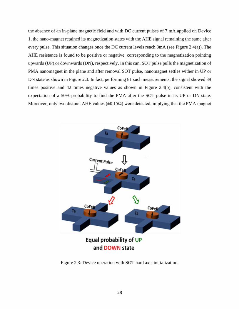
2.2 Deterministic and probabilistic SOT switching of PMA nano-magnets .......................... 27
2.3 Tuning probability of SOT switching via input terminal.................................................. 31
2.4 Directed network for neuromorphic computing ............................................................... 34
SPIN-ORBIT TORQUE CONTROLLED LOW BARRIER MTJ AS A P-BIT .................. 40
3.1 Experimental section ......................................................................................................... 40
3.2 SOT switching of a thermally stable MTJ (device 1) ....................................................... 42
3.3 SOT control of MTJ with low thermal stability (device 2) .............................................. 44
TOWARDS P-BITS WITH EMBEDDED MTJ ................................................................... 50
4.1 Introduction ....................................................................................................................... 51
4.2 Fabrication of PMA-MTJ ................................................................................................. 52
4.3 MoS2 transistor for in-chip p-bit ....................................................................................... 56
4.4 Annealing to tune magnetic anisotropy of PMA .............................................................. 58
COMPOUND SYNAPSE USING PROBABILISTIC SOT SWITCHING .......................... 62
5.1 Experimental Section ........................................................................................................ 63
5.2 Emulating synaptic behavior using probabilistic switching single nanomagnet .............. 64
5.3 Mathematical modeling of compound synapse................................................................. 67

7
5.4 Demonstration of 4-bit compound synapse ...................................................................... 68
5.5 Neural Network with p-bits and compound synapse ........................................................ 71
EFFICIENT SOT SWITCHING OF SEMICONDUCTING 2D FERROMAGNET ........... 75
6.1 Electrical characterization of CGT ................................................................................... 76
6.2 Anomalous Hall Effect in CGT/Ta heterostructure .......................................................... 78
6.3 SOT switching of CGT ..................................................................................................... 80
SUMMARY ........................................................................................................................... 88
REFERENCES ............................................................................................................................. 90
VITA ............................................................................................................................................. 98
PUBLICATIONS .......................................................................................................................... 99

8
LIST OF TABLES
Table 3.1: NIST STS randomness test and results (p-values) obtained from measuring the MTJ
with low thermal stability at 14 Oe (sample size~650 samples). If a p-value greater than 0.01 is
obtained, the test has been successfully passed. ........................................................................... 47
Table 5.1: Energy consumption comparison for weighted-sum operation in a 784×200×10 DBN.
....................................................................................................................................................... 73
9
LIST OF FIGURES
Figure 1.1: (a) von Neumann bottleneck: computer architecture with physically separated logic
and memory units is inefficient for data-centric computing (b) Challenges faced by CMOS scaling
i.e. logic units in recent years (Sources: Intel; press reports; Bob Colwell; Linley Group; IB
consulting; The Economist). (c) Ever increasing data and need for efficient data-centric computing
(Source: IDC #US44413318). ....................................................................................................... 17
Figure 1.2: (a) Pictorial representation of p-bit consisting Ii controlled WRITE unit and READ unit
with the output mi. (b) For Ii=0, p-bit fluctuate between 0 and 1 spending equal time in both states,
while (c) The time averaged value of mi as a function of the Ii shows a sigmoidal curve (Adapted
from [17]) ...................................................................................................................................... 18
Figure 1.3: Interconnected p-bits (Adopted from [18], © [2020] IEEE): for implementation of
Deep Belief Network to solve pattern recognition problems, Bayesian Networks for inference,
Ising computer for solving optimization problems and Invertible logic....................................... 19
Figure 1.4: Two p-bits/BSN designs using low energy barrier MTJ with fluctuating resistance: (a)
using SOT-MRAM type device (b) using STT-MRAM type device (Adopted from [24], © [2019]
IEEE)............................................................................................................................................. 20
Figure 1.5: Synaptic devices using high barrier MTJs (Adopted from [28], © [2015] IEEE). .... 21
Figure 1.6: (a)&(b) Deep Belief Network using MRAM-type devices with equivalent circuit for
the first layer using (c) p-bits as neurons and (d) compound synapses implemented with MRAM
cells (Adopted from [28]). ............................................................................................................ 22
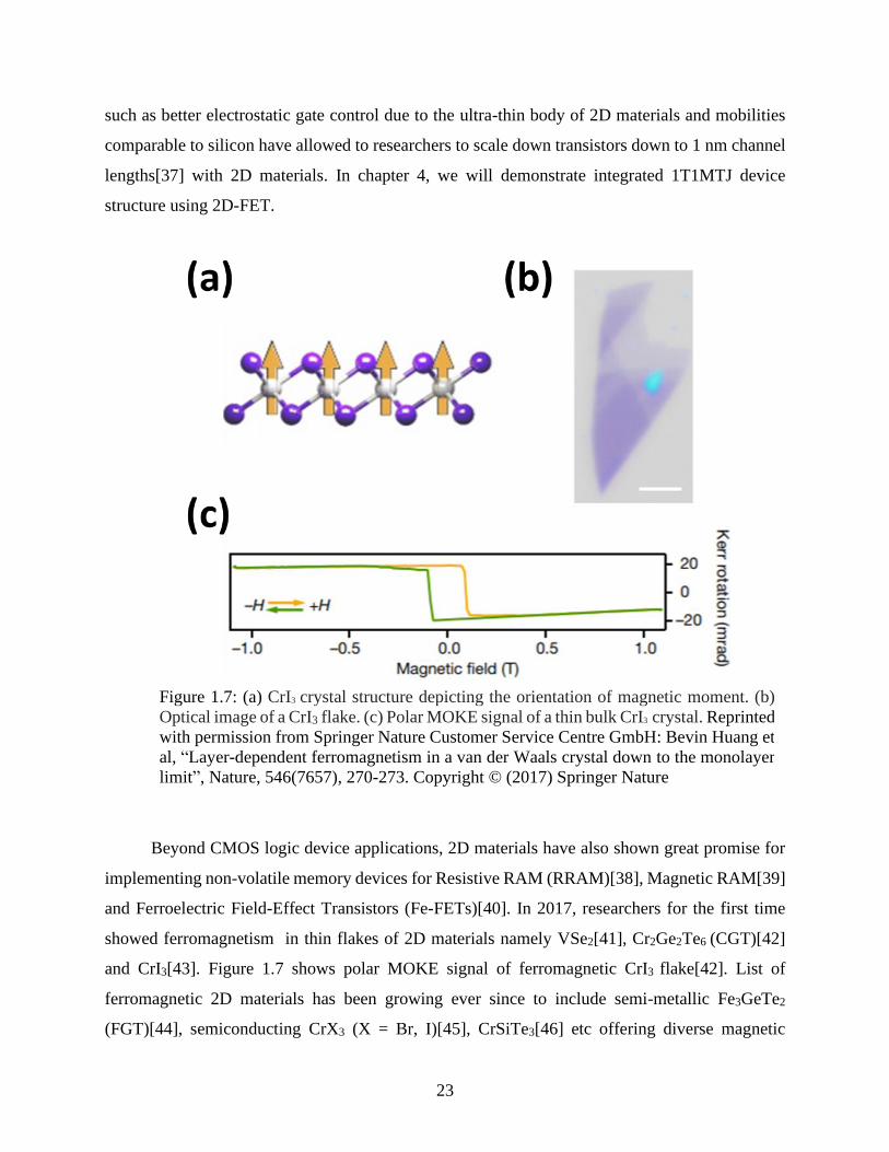
Figure 1.7: (a) CrI3 crystal structure depicting the orientation of magnetic moment. (b) Optical
image of a CrI3 flake. (c) Polar MOKE signal of a thin bulk CrI3 crystal (Reprinted with permission
from Springer Nature Customer Service Centre GmbH: Bevin Huang et al, “Layer-dependent
ferromagnetism in a van der Waals crystal down to the monolayer limit”, Nature, 546(7657), 270-
273.). Copyright © (2017) Springer Nature .................................................................................. 23
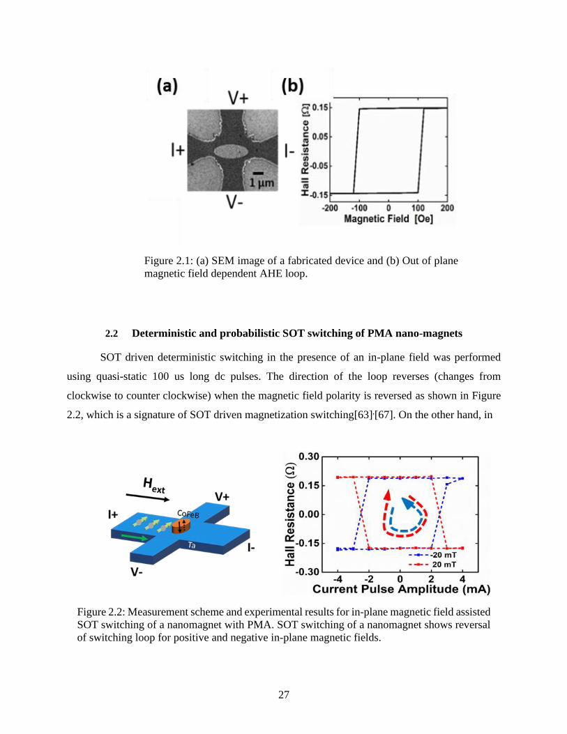
Figure 2.1: (a) SEM image of a fabricated device and (b) out of plane magnetic field dependent
AHE loop. ..................................................................................................................................... 27
Figure 2.2: Measurement scheme and experimental results for in-plane magnetic field assisted
SOT switching of a nanomagnet with PMA. SOT switching of a nanomagnet shows reversal of
switching loop for positive and negative in-plane magnetic fields............................................... 27
Figure 2.3: Device operation with SOT hard axis initialization. .................................................. 28
Figure 2.4: (a) Experimental measurement scheme consisting of a quasi-static current pulse
through the Hall bar for hard axis initialization, followed by an AC current to measure the
magnetization state. (b) Magnetization states of device 1, after each SOT pulse showing its
stochastic nature. ........................................................................................................................... 29
Figure 2.5: Magnetization states of device 2, after each SOT pulse for different current amplitudes
in absence of in-plane magnetic fields .......................................................................................... 30
10
Figure 2.6: (a) Cartoon of an all-electrical device with Oersted field generating metal ring to
control the final magnetization state after SOT pulse. (b) Average magnetization state of the device
(Dev 1) for different currents (Iin) through the Oersted ring. (c) Magnetization states after each
SOT pulse for Iin = -3.3 mA & +3.3 mA. ..................................................................................... 31
Figure 2.7: (a) Experimental set-up to measure average magnetization under external magnetic
field (Hext). (b) Average magnetization state of the device under Hext -impact for two different
magnet sizes. (c) sLLG simulations showing the magnetization dynamics. (d) sLLG simulation
results for magnets of sizes as shown in (b). ................................................................................ 33
Figure 2.8: (a) Two stochastic spin devices as described in the text used as binary stochastic
neurons. (b) Electrical inputs to the stochastic device, i.e. clock, Iin and READ. ........................ 34
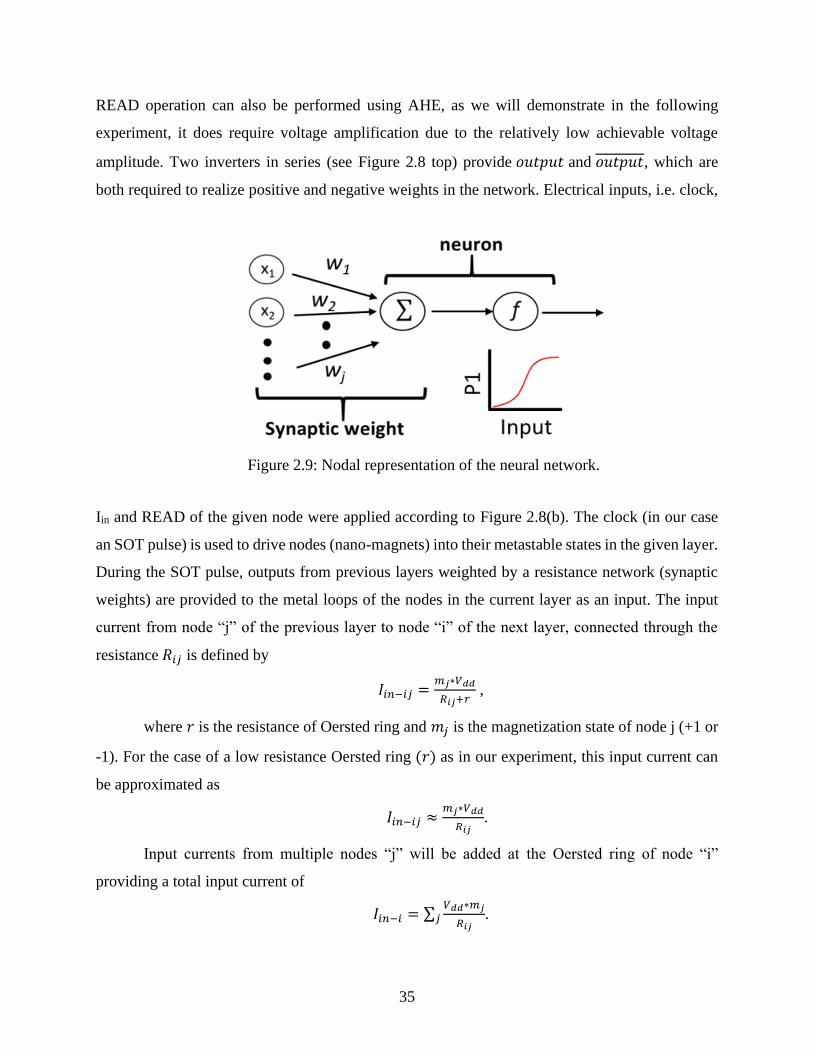
Figure 2.9: Nodal representation of the neural network. .............................................................. 35
Figure 2.10: Neural network implementation with spin devices as stochastic binary neurons and
resistive weight network. .............................................................................................................. 36
Figure 2.11: Experimental set up for two interacting devices. ..................................................... 37
Figure 2.12: Nodal representation and experimental measurements for (a) “+” ve weight, (b) “-”
ve weight and (c) 0 weight. ........................................................................................................... 38
Figure 3.1: (a) Material stack for our SOT-MTJ. (b) Schematic of SOT controlled MTJ. (c)
Scanning Electron Microscope (SEM) image of the MTJ and (d) major loop for TMR vs. magnetic
field (sweep rate = 480 Oe/min) of device 1. Copyright © [2019] IEEE. .................................... 41
Figure 3.2: (a) MTJ measurement set‐up for SOT switching. (b) Minor loop and (c) SOT switching
of stable MTJ (device 1) with quasi‐static current pulses (50 us wide) showing AP to P switching
for positive and P to AP switching for negative current pulses. Copyright © [2019] IEEE. ....... 42
Figure 3.3: (a) Minor B-field loop (sweep rate= 0.4 Oe/min) for a MTJ with low thermal stability
(device 2) with the SEM image. When the B-field is swept slowly during the minor loop
measurement, the MTJ with low thermal stability shows random fluctuations between the AP and
P states. The minor loop offset is around 14 Oe for this device size. (b) Zoom-in minor loop at Hext
of 14 Oe (to compensate for the minor loop offset at zero magnetic field) showing telegraphic
switching between the AP and the P state (red curve) and digitized data (black curve) to infer the
magnetization state of the free layer. Copyright © [2019] IEEE.................................................. 44
Figure 3.4: (a) Magnetization states obtained during near 1hr measurements at Hext=14 Oe. (b)
Obtained number of counts vs lifetime for AP (Red) and P (Green) states in semilog plot using
measurement in (a). At Hext = 14 Oe, sMTJ has equal characteristic lifetime for AP and P states.
Copyright © [2019] IEEE. ............................................................................................................ 45
Figure 3.5: (a) Magnetization states obtained at Hext =14 Oe for temperature of (a) 290 K (b) 300
K and (c) 320 K............................................................................................................................. 46
Figure 3.6: (a) MTJ with low thermal stability resistance data showing telegraphic switching
between the AP and P state for Hext = 14 Oe and different Idc flowing through the GSHE Ta layer.
(b) The probability for the MTJ with low thermal stability to be found in its AP state versus current
density flowing through Ta (black circles) based on data from (a) and expected probability
obtained using the analytical expression eq. 3 (red curve). Copyright © [2019] IEEE................ 48
11
Figure 4.1: (a) P-bit with embedded MTJ. (b) Output voltage at the transistor-drain as a function
of gate voltage (Vin) (c) Output voltage at the output node (Vout) as a function of gate voltage (Vin).
(Adapted from [23]) Copyright © [2019] IEEE. .......................................................................... 50
Figure 4.2: Process flow for fabrication of MTJs. ........................................................................ 52
Figure 4.3: (a) & (b) Optical and cross-sectional TEM of PMA-MTJ. (c) Major loop of TMR with
respect to out-of-plane magnetic field showing TMR of ~57%. .................................................. 53
Figure 4.4: (a) Optical image of PMA-MTJ (b) Magnetoresistance of MTJ in presence of in-plane
magnetic fields. ............................................................................................................................. 54
Figure 4.5: Process flow for fabrication of 2D-transistor on same chip as MTJs. ....................... 55
Figure 4.6: (a) Optical image of MoS2 transistor and (b) transfer characteristic of MoS2 ........... 56
Figure 4.7: (a)&(b) Schematic & optical image of integrated 1T/1MTJ structure. (c)&(d) MR of
the 1T/1MTJ structures in presence of in-plane magnetic fields for input gate voltages (Vgs) of 0
V and 30 V respectively. ............................................................................................................... 57
Figure 4.8: (a) Expected changes in the magnetic anisotropy of MTJ consisting of ferromagnets of
thicknesses of 0.85 nm and 1.65 nm separated by MgO tunnel barrier with annealing. (b) Expected
magnetic anisotropy of MTJ for different annealing times. ......................................................... 58
Figure 4.9: Magnetoresistance (MR) of MTJs annealed with respect to out-of-plane magnetic field
before annealing. Red arrows show “saturation point” for MR, used for determining magnetic
anisotropy of the free layer. .......................................................................................................... 59
Figure 4.10: Magnetoresistance (MR) of MTJs with respect to out-of-plane magnetic field
annealed for 5 mins ....................................................................................................................... 60
Figure 4.11: Annealing time dependent Hk of the free layer. ....................................................... 61
Figure 5.1: (a) Measurement set-up for SOT switching (b) SOT switching of a single nanomagnet
(binary memory unit). ................................................................................................................... 63
Figure 5.2: (a) Modified pulsed scheme to characterize probabilistic nature of SOT switching (b)
(b) Switching probability (Psw) curve for two different current pulse widths. ............................. 64
Figure 5.3: (a) Measurement scheme to emulate compound synapse using SOT device with single
nanomagnet. (b) Compound synapse consisting multiple stochastic binary unit. (c) Experimental
data on magnetization state with pulse number for measurement scheme shown in (a). ............. 65
Figure 5.4: Experimental potentiation and depression curves derived using results shown in 5.3(c).
....................................................................................................................................................... 66
Figure 5.5: (a) Pulse scheme I: identical pulses. (b) Expected P and D curve for 100 cycles showing
non-linearity (c) Pulse scheme II: incremental pulses. (d) Expected P and D curve for 100 cycles
with incremental pulse scheme showing better symmetry and linearity. ..................................... 68
Figure 5.6: Scanning electron microscope (SEM) image of our SOT based synapse with 16
nanomagnets. (b) Anomalous Hall effect vs. out-of-plane magnetic field for the device showing
110 mOhm steps, corresponding to individual nanomagnet switching. ....................................... 69
12
Figure 5.7: Potentiation and depression curve of the device using identical pulse scheme (pulse
scheme I) ....................................................................................................................................... 69
Figure 5.8: Potentiation and depression curve of the device using incremental pulse scheme (pulse
scheme II)...................................................................................................................................... 70
Figure 5.9: (a) Graph representation of the 784×200×10 DBN. (b) Equivalent circuit for the first
layer with p-bits as neurons and (d) compound synapse implemented with MRAM cells. ......... 71
Figure 5.10: (a) Error rate versus resistance-area-product. (b) Error rate versus tunneling magneto
resistance (TMR) for a 784×200×10 DBN with 4-bit compound synapses. ................................ 72
Figure 6.1: (a) 3D schematic of our back-gated FET with semiconducting CGT channel and Ru
contacts. (b) Optical image of the actual device under investigation. © 2020 WILEY‐VCH Verlag
GmbH & Co. KGaA, Weinheim ................................................................................................... 75
Figure 6.2: (c) Transfer characteristics of the device for temperatures of 10 K, 80 K, 150 K and
300K for Vds=100 mV. (d) Non-linear Ids-Vds characteristics at 10 K for Vgs=0 V. (Inset:
Temperature dependence of 2-terminal resistance of the device at Vgs=0 V. © 2020 WILEY‐VCH
Verlag GmbH & Co. KGaA, Weinheim ....................................................................................... 76
Figure 6.3: Temperature dependence of CGT 4-probe resistance measured using a Keithely 6221
as AC current source and an SR830 lock-in set-up: Since the input impedance of the SR830 is 10
MOhm, 4-probe measurements were not performed at lower temperature. © 2020 WILEY‐VCH
Verlag GmbH & Co. KGaA, Weinheim ....................................................................................... 77
Figure 6.4: (a) 3D schematic and optical image of a fabricated Hall bar device from a CGT/Ta
heterostructure and measurement set-up. (b) Raman spectrum of the CGT/Ta heterostructure
device. (Inset: Raman spectrum of a CGT flake that was exposed to air). (c) Atomic force
microscopy image of the device surface showing sub-nanometer roughness. © 2020 WILEY‐VCH
Verlag GmbH & Co. KGaA, Weinheim ....................................................................................... 78
Figure 6.5: (a) Temperature dependent Hall resistance of the Hall bar device consisting 50 nm
thick CGT with out-of-plane magnetic field. Anomalous Hall effect start to emerge around 70 K,
near Curie temperature of CGT. (b) Normalized RAHE of for three different thicknesses of CGT. ©
2020 WILEY‐VCH Verlag GmbH & Co. KGaA, Weinheim. ..................................................... 79
Figure 6.6: (a) AFM image of device #3 (b) Hall resistance versus Hz measured at Iac= 4 uA using
a lock-in set-up for Idc=+/-50 uA. (c) Hall resistance versus Hx measured at Iac = 4 uA using a lock-
in set-up for Idc=+/-100 uA. (d) Hall resistance versus Hx measured ath Iac= 4 uA using a lock-in
set-up for Idc= +/-100 uA. All measurements were performed at 10K. © 2020 WILEY‐VCH Verlag
GmbH & Co. KGaA, Weinheim. .................................................................................................. 82
Figure 6.7: In-plane magnetic field dependence of second harmonic of Hall voltage. ................ 83
Figure 6.8: (a) Field assisted SOT switching of out-of-plane magnetization with Idc= +/- 100 uA at
4K. (b) Idc dependent field assisted SOT switching at 4K. (c) Temperature dependent field assisted
SOT switching at T=4 K, 40 K and 80 K. © 2020 WILEY‐VCH Verlag GmbH & Co. KGaA,
Weinheim. ..................................................................................................................................... 84

13
Figure 6.9: (a) Phase diagram of mz for applied Idc and Hx. (b) Required current densities and in-
plane fields for SOT switching of previously reported magnetic heterostructure. © 2020 WILEY‐
VCH Verlag GmbH & Co. KGaA, Weinheim. ............................................................................ 86
14
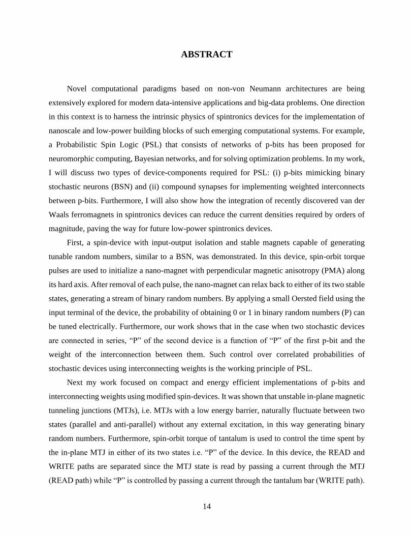
ABSTRACT
Novel computational paradigms based on non-von Neumann architectures are being
extensively explored for modern data-intensive applications and big-data problems. One direction
in this context is to harness the intrinsic physics of spintronics devices for the implementation of
nanoscale and low-power building blocks of such emerging computational systems. For example,
a Probabilistic Spin Logic (PSL) that consists of networks of p-bits has been proposed for
neuromorphic computing, Bayesian networks, and for solving optimization problems. In my work,
I will discuss two types of device-components required for PSL: (i) p-bits mimicking binary
stochastic neurons (BSN) and (ii) compound synapses for implementing weighted interconnects
between p-bits. Furthermore, I will also show how the integration of recently discovered van der
Waals ferromagnets in spintronics devices can reduce the current densities required by orders of
magnitude, paving the way for future low-power spintronics devices.
First, a spin-device with input-output isolation and stable magnets capable of generating
tunable random numbers, similar to a BSN, was demonstrated. In this device, spin-orbit torque
pulses are used to initialize a nano-magnet with perpendicular magnetic anisotropy (PMA) along
its hard axis. After removal of each pulse, the nano-magnet can relax back to either of its two stable
states, generating a stream of binary random numbers. By applying a small Oersted field using the
input terminal of the device, the probability of obtaining 0 or 1 in binary random numbers (P) can
be tuned electrically. Furthermore, our work shows that in the case when two stochastic devices
are connected in series, “P” of the second device is a function of “P” of the first p-bit and the
weight of the interconnection between them. Such control over correlated probabilities of
stochastic devices using interconnecting weights is the working principle of PSL.
Next my work focused on compact and energy efficient implementations of p-bits and
interconnecting weights using modified spin-devices. It was shown that unstable in-plane magnetic
tunneling junctions (MTJs), i.e. MTJs with a low energy barrier, naturally fluctuate between two
states (parallel and anti-parallel) without any external excitation, in this way generating binary
random numbers. Furthermore, spin-orbit torque of tantalum is used to control the time spent by
the in-plane MTJ in either of its two states i.e. “P” of the device. In this device, the READ and
WRITE paths are separated since the MTJ state is read by passing a current through the MTJ
(READ path) while “P” is controlled by passing a current through the tantalum bar (WRITE path).
15
Hence, a BSN/p-bit is implemented without energy-consuming hard axis initialization of the
magnet and Oersted fields. Next, probabilistic switching of stable magnets was utilized to
implement a novel compound synapse, which can be used for weighted interconnects between p-
bits. In this experiment, an ensemble of nano-magnets was subjected to spin-orbit torque pulses
such that each nano-magnet has a finite probability of switching. Hence, when a series of pulses
are applied, the total magnetization of the ensemble gradually increases with the number of pulses
applied similar to the potentiation and depression curves of synapses. Furthermore, it was shown
that a modified pulse scheme can improve the linearity of the synaptic behavior, which is desired
for neuromorphic computing. By implementing both neuronal and synaptic devices using simple
nano-magnets, we have shown that PSL can be realized using a modified Magnetic Random
Access Memory (MRAM) technology. Note that MRAM technology exists in many current
foundries.
To further reduce the current densities required for spin-torque devices, we have fabricated
heterostructures consisting of a 2-dimensional semiconducting ferromagnet (Cr2Ge2Te6) and a
metal with spin-orbit coupling metal (tantalum). Because of properties such as clean interfaces,
perfect crystalline nano-magnet structure and sustained magnetic moments down to the mono-
layer limit and low current shunting, 2D ferromagnets require orders of magnitude lower current
densities for spin-orbit torque switching than conventional metallic ferromagnets such as CoFeB.
16
INTRODUCTION
Since 1971, scaling of CMOS transistors have enabled exponential increase in number of
transistors per integrated chip[1] consistent with Moore’s law and led to better performance in
terms of speed and power consumption. Even though advanced CMOS technology node is
expected to scale down from current 7 nm to 5 nm or even 3 nm in coming year[2], such scaling
is slowing down due to fundamental device physics, increased power densities and economic
issues such as difficulties in cost-effective way for production etc[3]. At the same time, amount of
data being generated by businesses, media, IOTs etc. is expected to double every two years[4].
Extracting relevant information from gathered data hold promise for achieving new levels
efficiencies and products among various sectors such as finance, healthcare, manufacturing
processes etc [5]. To this end, artificial intelligence, a branch of computer science has facilitated
difficult pattern recognition, learning using large amount of data[6]. However, such data-centric
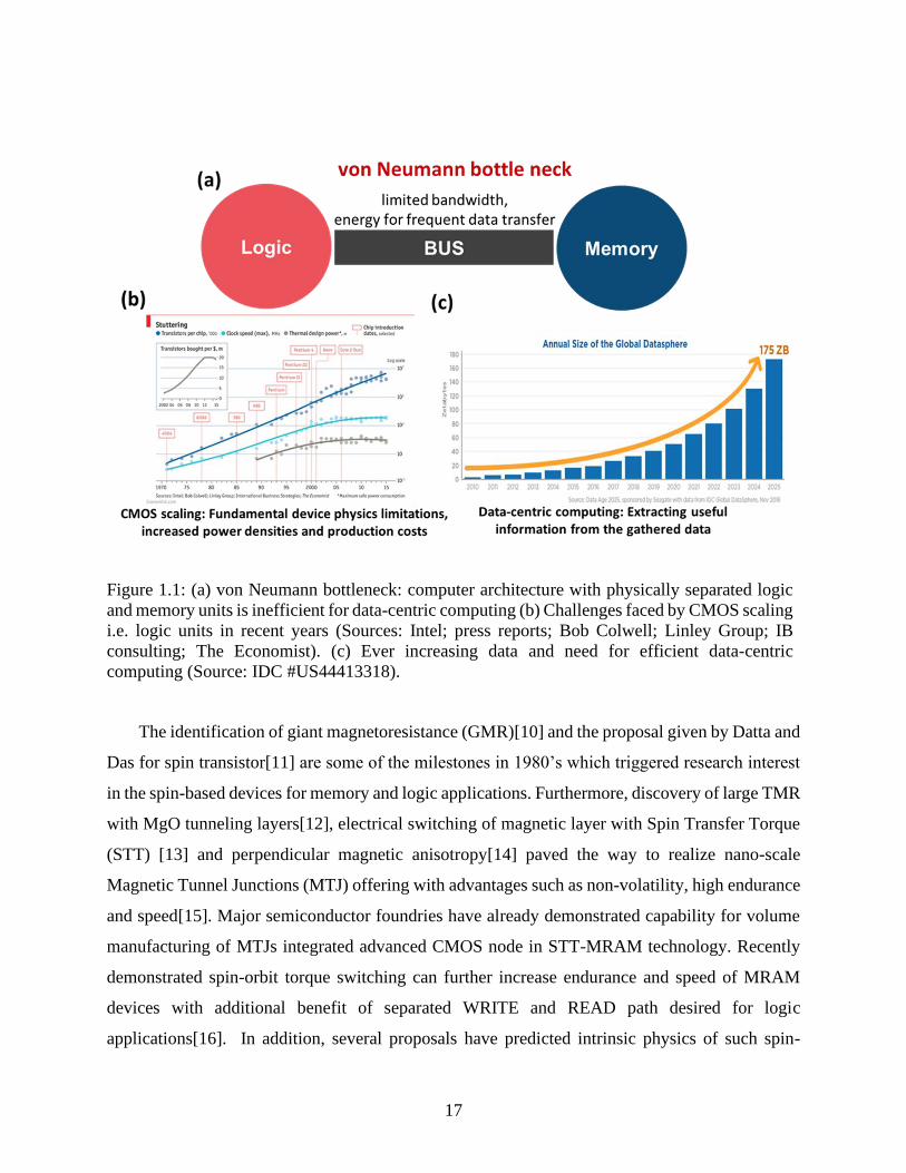
computing is being implemented using von Neumann based computer architecture as shown in
Figure 1.1, which separates memory and processing unit[7]. Limited bandwidth and huge energy
required for frequent data transfer between the CPU and memory units are some of the limiting
factors for efficient data-centric computation[8]. Faced with dual challenges of slow-down of
CMOS scaling and emergence of data-centric computing, alternative non-von Neumann
computing architectures with physically close processing and memory units such as neuromorphic
computing[8], in-memory computing[9] etc have been extensively explored by researchers in
recent years. Such unconventional computing systems offer significant benefits in-terms of
performance (speed and power) for data-centric computing and has triggered extensive search for
novel (i) logic devices such as spiking neurons, oscillators capable of performing more-than-
Boolean operations and (ii) memory devices such as analog non-volatile memory which will
become building-blocks for unconventional computing systems. Towards that goal, spintronic
devices have emerged as potential candidates for both logic and memory units.
17
The identification of giant magnetoresistance (GMR)[10] and the proposal given by Datta and
Das for spin transistor[11] are some of the milestones in 1980’s which triggered research interest
in the spin-based devices for memory and logic applications. Furthermore, discovery of large TMR
with MgO tunneling layers[12], electrical switching of magnetic layer with Spin Transfer Torque
(STT) [13] and perpendicular magnetic anisotropy[14] paved the way to realize nano-scale
Magnetic Tunnel Junctions (MTJ) offering with advantages such as non-volatility, high endurance
and speed[15]. Major semiconductor foundries have already demonstrated capability for volume
manufacturing of MTJs integrated advanced CMOS node in STT-MRAM technology. Recently
demonstrated spin-orbit torque switching can further increase endurance and speed of MRAM
devices with additional benefit of separated WRITE and READ path desired for logic
applications[16]. In addition, several proposals have predicted intrinsic physics of such spin-
Figure 1.1: (a) von Neumann bottleneck: computer architecture with physically separated logic
and memory units is inefficient for data-centric computing (b) Challenges faced by CMOS scaling
i.e. logic units in recent years (Sources: Intel; press reports; Bob Colwell; Linley Group; IB
consulting; The Economist). (c) Ever increasing data and need for efficient data-centric
computing (Source: IDC #US44413318).
18
devices can mimic neural, oscillatory, or synaptic functionalities[17]. This work mainly focuses
on experimental demonstration of spin-devices mimicking such functionalities with potential of
being building blocks for unconventional computing. In the following section, we will introduce
probabilistic spin logic (PSL) proposed by Prof Datta’s group[17] and will discuss implementation
of device components required for PSL using MRAM type devices. Finally, newly discovered
ferromagnetic 2-dimentional materials for future low-power spin-devices will be discussed.
1.1 Probabilistic Spin Logic
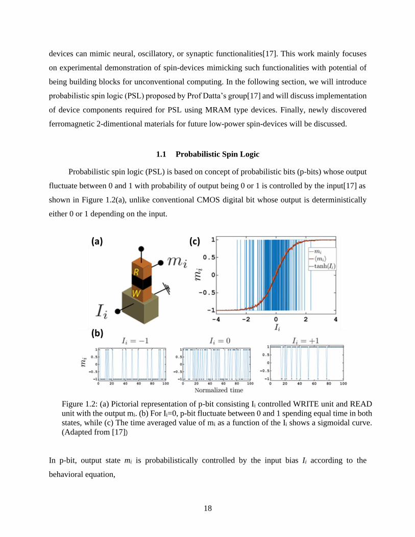
Probabilistic spin logic (PSL) is based on concept of probabilistic bits (p-bits) whose output
fluctuate between 0 and 1 with probability of output being 0 or 1 is controlled by the input[17] as
shown in Figure 1.2(a), unlike conventional CMOS digital bit whose output is deterministically
either 0 or 1 depending on the input.
In p-bit, output state mi is probabilistically controlled by the input bias Ii according to the
behavioral equation,
Figure 1.2: (a) Pictorial representation of p-bit consisting Ii controlled WRITE unit and READ
unit with the output mi. (b) For Ii=0, p-bit fluctuate between 0 and 1 spending equal time in both
states, while (c) The time averaged value of mi as a function of the Ii shows a sigmoidal curve.
(Adapted from [17])
19
𝑚𝑖 = 𝑠𝑔𝑛 {tanh (𝐼𝑖) + 𝑟)}
where r is a random number uniformly distributed between −1 and 1. Here, we are using
bipolar variables mi = ±1 to represent the 0 and 1 states. From eqn. 1.1, for zero input bias i.e. Ii =
0, mi randomly fluctuates between +1 and -1 with equal probability and hence time-average of mi
(represented by ⟨𝑚𝑖⟩ ) is 0. However, for positive input bias (Ii > 0), mi is more likely to be +1 than
-1 resulting in ⟨𝑚𝑖⟩ > 0 (Figure 1.2(b)), while negative input bias (Ii < 0) results in ⟨𝑚𝑖⟩ < 0
(Figure 1.2(b)). Overall, as shown in Figure 1.2(c), ⟨𝑚𝑖⟩ is sigmoidal function of input Ii meaning
𝑚𝑖 can be pinned to either +1 or -1 using strong enough positive or negative bias respectively.
Effectively p-bit is a three terminal tunable random generator with important property of input-
output isolation analogous to Binary Stochastic Neuron (BSN)[5]. This allows construction of
interconnected networks of p-bits according to the equation,
𝐼𝑖 = ∑𝑊𝑖𝑗𝑚𝑗 + ℎ𝑖
where 𝑊𝑖𝑗 is the weight of the interconnect connecting output of jth p-bit to input of ith p-bit and
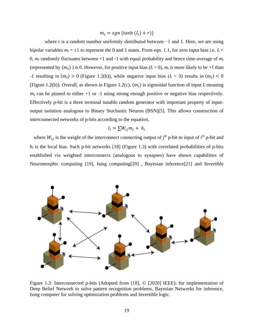
hi is the local bias. Such p-bit networks [18] (Figure 1.3) with correlated probabilities of p-bits
established via weighted interconnects (analogous to synapses) have shown capabilities of
Neuromorphic computing [19], Ising computing[20] , Bayesian inference[21] and Invertible
Figure 1.3: Interconnected p-bits (Adopted from [18], © [2020] IEEE): for implementation of
Deep Belief Network to solve pattern recognition problems, Bayesian Networks for inference,
Ising computer for solving optimization problems and Invertible logic.
20
logic[22]. In chapter 2, we demonstrate proof-of-concept three terminal spin-device capable of
generating tunable binary random numbers with input-output isolation similar to a p-bit.
Furthermore, we show correlated probability between two such devices controlled via
resistive/weighted interconnect as required for implementation PSL.
1.2 Realization of device components (neurons and synapses) of PSL using stochastic
MRAM type devices
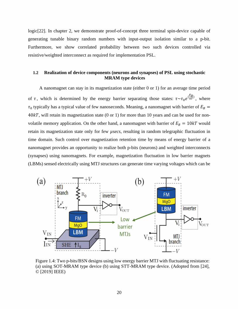
A nanomagnet can stay in its magnetization state (either 0 or 1) for an average time period
of 𝜏 , which is determined by the energy barrier separating those states: 𝜏~𝜏0𝑒(𝐸𝐵𝑘𝑇
), where
𝜏0 typically has a typical value of few nanoseconds. Meaning, a nanomagnet with barrier of 𝐸𝐵 =
40𝑘𝑇, will retain its magnetization state (0 or 1) for more than 10 years and can be used for non-
volatile memory application. On the other hand, a nanomagnet with barrier of 𝐸𝐵 = 10𝑘𝑇 would
retain its magnetization state only for few µsecs, resulting in random telegraphic fluctuation in
time domain. Such control over magnetization retention time by means of energy barrier of a
nanomagnet provides an opportunity to realize both p-bits (neurons) and weighted interconnects
(synapses) using nanomagnets. For example, magnetization fluctuation in low barrier magnets
(LBMs) sensed electrically using MTJ structures can generate time varying voltages which can be
Figure 1.4: Two p-bits/BSN designs using low energy barrier MTJ with fluctuating resistance:
(a) using SOT-MRAM type device (b) using STT-MRAM type device. (Adopted from [24],
© [2019] IEEE)
21
used for random number generation. Several proposals have explored implementation of p-bits
using such low-barrier nano-magnets in STT-MRAM or SOT-MRAM type devices [22][23][24].
Figure 1.4 shows two of such p-bit designs. By engineering low enough energy barrier, fluctuation
rates in low-barrier MTJs can be in sub-nanoseconds timescale[25]. Since STT-MRAM is close to
foundry scale production [15] and wafer-scale manufacturability has been shown even for SOT-
MRAM[26], realization of neural device (p-bits) using MTJs is highly desirable.
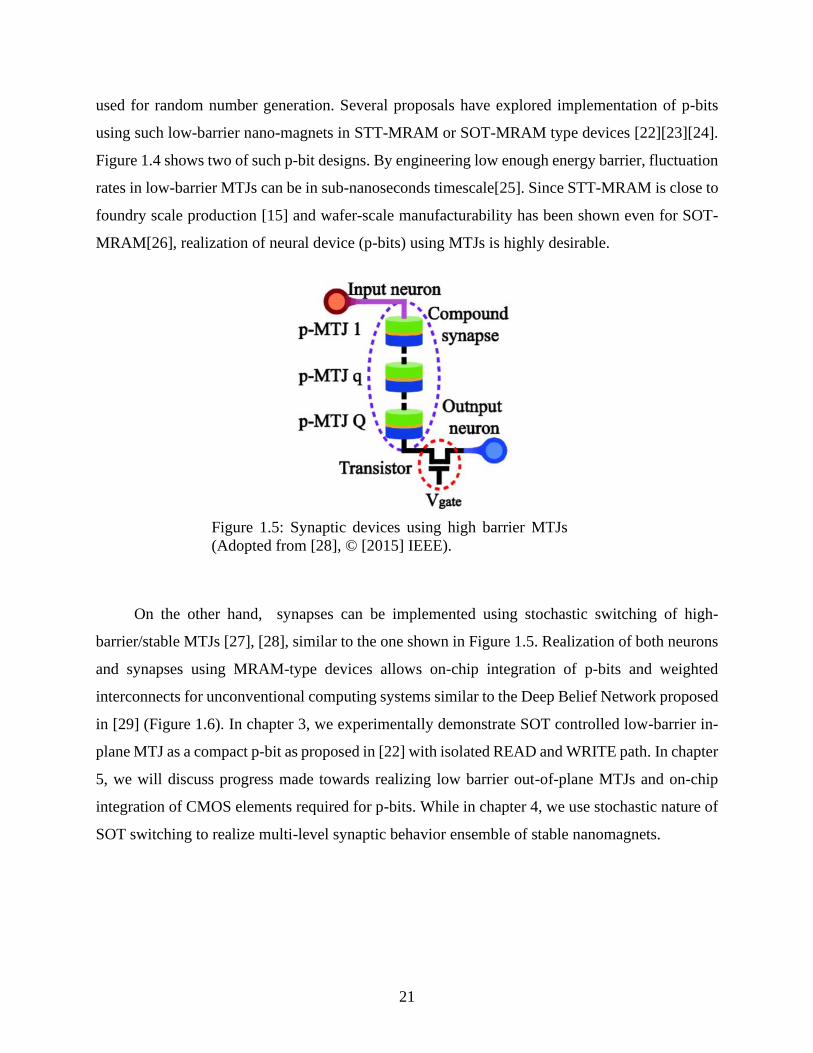
On the other hand, synapses can be implemented using stochastic switching of high-
barrier/stable MTJs [27], [28], similar to the one shown in Figure 1.5. Realization of both neurons
and synapses using MRAM-type devices allows on-chip integration of p-bits and weighted
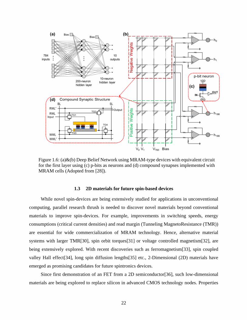
interconnects for unconventional computing systems similar to the Deep Belief Network proposed
in [29] (Figure 1.6). In chapter 3, we experimentally demonstrate SOT controlled low-barrier in-
plane MTJ as a compact p-bit as proposed in [22] with isolated READ and WRITE path. In chapter
5, we will discuss progress made towards realizing low barrier out-of-plane MTJs and on-chip
integration of CMOS elements required for p-bits. While in chapter 4, we use stochastic nature of
SOT switching to realize multi-level synaptic behavior ensemble of stable nanomagnets.
Figure 1.5: Synaptic devices using high barrier MTJs
(Adopted from [28], © [2015] IEEE).
22
1.3 2D materials for future spin-based devices
While novel spin-devices are being extensively studied for applications in unconventional
computing, parallel research thrush is needed to discover novel materials beyond conventional
materials to improve spin-devices. For example, improvements in switching speeds, energy
consumptions (critical current densities) and read margin (Tunneling MagnetoResistance (TMR))
are essential for wide commercialization of MRAM technology. Hence, alternative material
systems with larger TMR[30], spin orbit torques[31] or voltage controlled magnetism[32], are
being extensively explored. With recent discoveries such as ferromagnetism[33], spin coupled
valley Hall effect[34], long spin diffusion lengths[35] etc., 2-Dimensional (2D) materials have
emerged as promising candidates for future spintronics devices.
Since first demonstration of an FET from a 2D semiconductor[36], such low-dimensional
materials are being explored to replace silicon in advanced CMOS technology nodes. Properties
Figure 1.6: (a)&(b) Deep Belief Network using MRAM-type devices with equivalent circuit
for the first layer using (c) p-bits as neurons and (d) compound synapses implemented with
MRAM cells (Adopted from [28]).
23
such as better electrostatic gate control due to the ultra-thin body of 2D materials and mobilities
comparable to silicon have allowed to researchers to scale down transistors down to 1 nm channel
lengths[37] with 2D materials. In chapter 4, we will demonstrate integrated 1T1MTJ device
structure using 2D-FET.
Beyond CMOS logic device applications, 2D materials have also shown great promise for
implementing non-volatile memory devices for Resistive RAM (RRAM)[38], Magnetic RAM[39]
and Ferroelectric Field-Effect Transistors (Fe-FETs)[40]. In 2017, researchers for the first time
showed ferromagnetism in thin flakes of 2D materials namely VSe2[41], Cr2Ge2Te6 (CGT)[42]
and CrI3[43]. Figure 1.7 shows polar MOKE signal of ferromagnetic CrI3 flake[42]. List of
ferromagnetic 2D materials has been growing ever since to include semi-metallic Fe3GeTe2
(FGT)[44], semiconducting CrX3 (X = Br, I)[45], CrSiTe3[46] etc offering diverse magnetic
Figure 1.7: (a) CrI3 crystal structure depicting the orientation of magnetic moment. (b)
Optical image of a CrI3 flake. (c) Polar MOKE signal of a thin bulk CrI3 crystal. Reprinted
with permission from Springer Nature Customer Service Centre GmbH: Bevin Huang et
al, “Layer-dependent ferromagnetism in a van der Waals crystal down to the monolayer
limit”, Nature, 546(7657), 270-273. Copyright © (2017) Springer Nature
24
properties as well. For example, VSe2 has in-plane anisotropy while Cr2Ge2Te6[42] and CrI3[43]
possess perpendicular magnetic anisotropy. Furthermore, magnetic properties of semiconducting
2D ferromagnets such as Curie temperature or anisotropy can be manipulated using electrostatic
fields[47]. With their ability to form 2D heterostructures, 2D materials provide unique
opportunities to realize not just conventional spintronics devices such as MTJs but also novel logic
and memory device concepts. For example, MTJs were experimentally demonstrated using a vdW
heterostructure consisting of a FGT/hBN/FGT stack (Figure 4(a)) with FGT as FM and hBN as
tunnel barrier[48] while S. Jiang et al. have successfully demonstrated a non-volatile spin-
transistor i.e. gate-controlled tunnel conductance[49]. Furthermore, vdW heterostructures such as
FGT/hBN/FGT with the perfect crystalline nature and potentially clean interfaces are expected to
exhibit much larger TMR ratios (up to ~ 6250%)[50] compared to conventional CoFeB-MgO
based MTJs.
Being able to electrically manipulate the magnetic properties in recently discovered 2D
ferromagnets is essential for their integration in future spintronics devices. In chapter 5, the
magnetization of a semiconducting 2D ferromagnet, namely CGT, is studied using the anomalous
Hall effect in CGT/Tantalum heterostructures and we will also show SOT switching of such
semiconducting 2D ferromagnet CGT with required switching current densities order of magnitude
lower than conventional metal, underscoring potential of 2D materials for future spintronics
devices.
25
PROBABILISTIC BIT USING HARD AXIS INITIALIZATION AND
CORRELATED PROBABILITIES VIA WEIGHTED
INTERCONNECTS
Most of the material in this chapter has been reprinted from [51]: Ostwal Vaibhav et al., "Spin-
torque devices with hard axis initialization as Stochastic Binary Neurons." Scientific reports (2018)
8:16689. This article is distributed under a Creative Commons Attribution CC BY license.
Emerging spintronic devices have recently attracted attention for efficient implementation
of more-than-Boolean computational systems such as neural networks[52], Bayesian
networks[53][54][55], Ising networks[56][55][57], and invertible logic[58]. Key to the
implementation of such systems is the stochastic nature of the network building blocks[59][60][61]
- nano-magnets in this demonstration – in response to an external stimulation. The desired output
characteristics display a sigmoidal probability to find the nano-magnet in one or the other
magnetization state – here as a function of an input current. One approach is to drive the nano-
magnet into its metastable state through hard axis initialization and let it relax in the presence of
an input current, which determines the probability of the nano-magnet settling to one of the states,
(+mi) or (-mi)[55][62]. Here, we will present proof-of-concept spin-devices that employ SOT for
hard-axis initialization and a current induced Oersted field to control their output states. Spin
devices using this approach emulate the functionality of a stochastic binary neuron with the
average output modelled by equation 𝑦 = 𝑓(∑ 𝑤𝑖𝑗𝑥𝑗 + 𝑏𝑖𝑗 ), where f is the sigmoidal function, wij
is the synaptic weight corresponding to the input node xi, and bi is the default bias. Along this idea,
directed networks consisting of spin devices with weighted interconnection can be demonstrated.
In heavy metal (HM)/ferromagnet (FM) systems, spin orbit torque (SOT) switching
through the spin Hall effect (SHE) in the HM is an efficient method to control the magnetization
of the FM[63],[64]. However, since the generated spin is always polarized along the surface plane,
magnets with perpendicular magnetic anisotropy (PMA) cannot be deterministically switched. A
symmetry breaking in-plane magnetic field is therefore required for SOT switching in HM/ PMA-
FM stacks[63]. However, if deterministic switching is not required, currents at levels beyond those
typically required for field-assisted switching can drive PMA magnets into their metastable in-
plane magnetization states through SOT [65],[66]. Once the SOT current is removed, the PMA
magnet can relax back to one of the two stable states, (+mi) and (-mi), with a 50%/50% probability
26
in a purely random fashion that is entirely determined by thermal noise. In this way, a true “random
number generator” is created. On the other hand, if the SOT current is removed while a small
external perpendicular magnetic field is present, a magnetization in the same direction as the
applied field will be preferred with a probability distribution determined by the field strength. To
generate a local, perpendicular Oersted field, a small metal loop that is isolated through a SiO2
layer from the nano-magnet is used in our device layout as the input terminal. In this way, input-
output isolation is ensured, which is one of the requirements to interconnect building blocks into
networks for the applications proposed in[52][55]. In order to show that a spin device is a natural
analogue to a stochastic binary neuron, two of these devices are interconnected in this article to
form a directed network, and their basic operations are demonstrated.
2.1 Experimental Section
A material stack of Ta(7)/CoFeB(1)/MgO(2)/Ta(2) (numbers in brackets denote the
respective film thicknesses in nm) was defined on a Si/SiO2 substrate using a physical vapor
deposition sputter system at a base pressure of 3*10-8 Torr. The CoFeB thickness of 1 nm was
chosen to induce PMA and confirmed by measuring the magnetic moment (M) versus magnetic
field (H) loop of an un-patterned film using a SQUID measurement set-up. The film stack was
patterned into Hall bars by e-beam lithography using a bilayer resist stack of polymethyl
methacrylate (PMMA) and hydrogen silsesquioxane (HSQ), followed by Argon (Ar) ion beam
etching down to the SiO2 surface. Next, elliptical PMA magnets of various sizes ranging from 0.5
um*1.2 um to 1 um*3 um were patterned using the same lithography and etching process as before
until the bottom Ta (7 nm) layer was reached. Last, electrical contacts were defined using e-beam
lithography and a lift-off process after depositing Ti (20 nm)/Au (100 nm) metal stacks. Figure
2.1(a) shows a scanning electron microscopy (SEM) image of a fabricated device as well as a
schematic illustration of the device during the measurement procedure described in the previous
paragraph. An elliptical shape was chosen so that the nano-magnet covered the width of the voltage
arm entirely and at the same time was located far enough from the edges of the current arm of the
Hall bar to minimize the out-of-plane Oersted field due to currents through the Hall bar. To detect
the magnetization state of the PMA nano-magnet, the anomalous Hall effect (AHE) is used (Figure
2.1(b)).
27
2.2 Deterministic and probabilistic SOT switching of PMA nano-magnets
SOT driven deterministic switching in the presence of an in-plane field was performed
using quasi-static 100 us long dc pulses. The direction of the loop reverses (changes from
clockwise to counter clockwise) when the magnetic field polarity is reversed as shown in Figure
2.2, which is a signature of SOT driven magnetization switching[63],[67]. On the other hand, in
Figure 2.2: Measurement scheme and experimental results for in-plane magnetic field assisted
SOT switching of a nanomagnet with PMA. SOT switching of a nanomagnet shows reversal
of switching loop for positive and negative in-plane magnetic fields.
Figure 2.1: (a) SEM image of a fabricated device and (b) Out of plane
magnetic field dependent AHE loop.
28
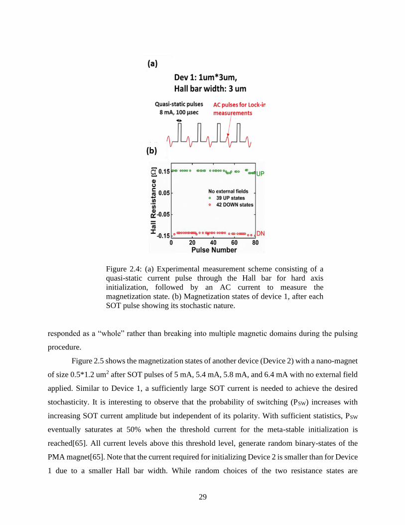
the absence of an in-plane magnetic field and with DC current pulses of 7 mA applied on Device
1, the nano-magnet retained its magnetization states with the AHE signal remaining the same after
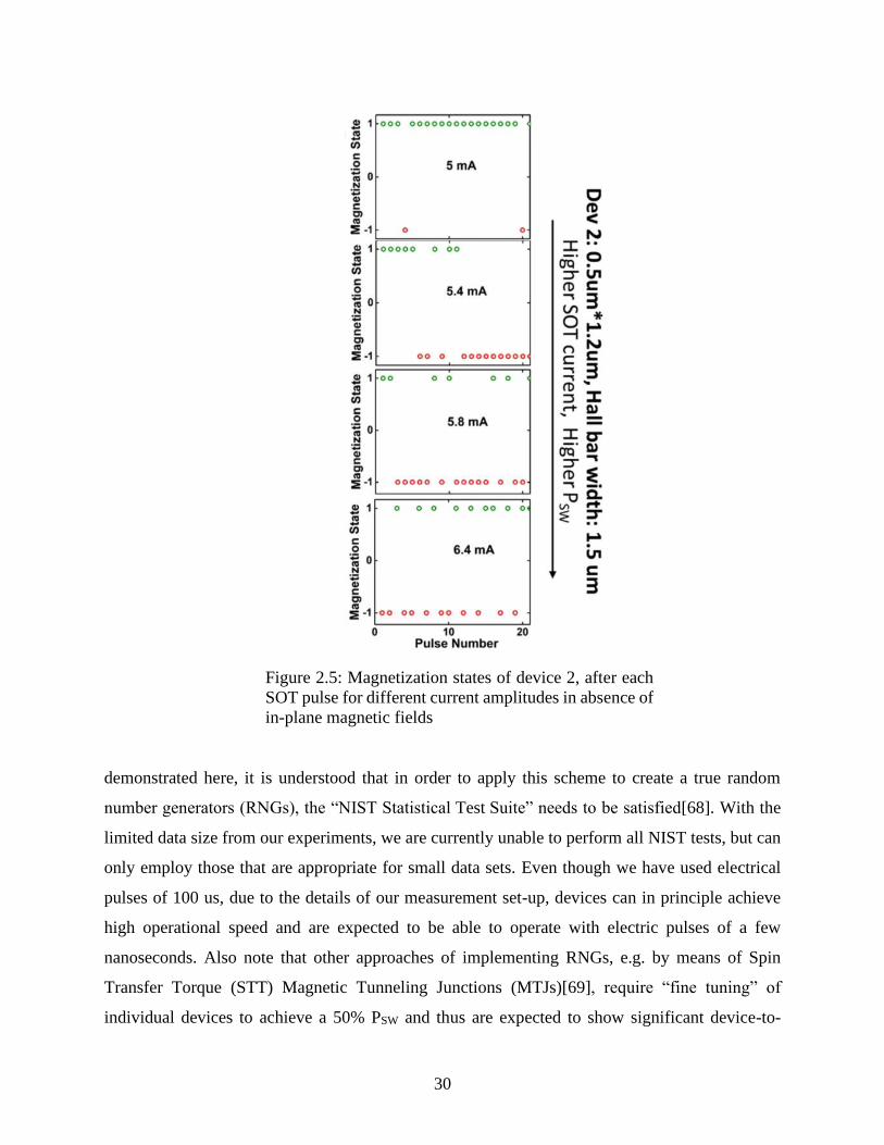
every pulse. This situation changes once the DC current levels reach 8mA (see Figure 2.4(a)). The
AHE resistance is found to be positive or negative, corresponding to the magnetization pointing
upwards (UP) or downwards (DN), respectively. In this can, SOT pulse pulls the magnetization of
PMA nanomagnet in the plane and after removal SOT pulse, nanomagnet settles wither in UP or
DN state as shown in Figure 2.3. In fact, performing 81 such measurements, the signal showed 39
times positive and 42 times negative values as shown in Figure 2.4(b), consistent with the
expectation of a 50% probability to find the PMA after the SOT pulse in its UP or DN state.
Moreover, only two distinct AHE values (±0.15Ω) were detected, implying that the PMA magnet
Figure 2.3: Device operation with SOT hard axis initialization.
29
responded as a “whole” rather than breaking into multiple magnetic domains during the pulsing
procedure.
Figure 2.5 shows the magnetization states of another device (Device 2) with a nano-magnet
of size 0.5*1.2 um2 after SOT pulses of 5 mA, 5.4 mA, 5.8 mA, and 6.4 mA with no external field
applied. Similar to Device 1, a sufficiently large SOT current is needed to achieve the desired
stochasticity. It is interesting to observe that the probability of switching (PSW) increases with
increasing SOT current amplitude but independent of its polarity. With sufficient statistics, PSW
eventually saturates at 50% when the threshold current for the meta-stable initialization is
reached[65]. All current levels above this threshold level, generate random binary-states of the
PMA magnet[65]. Note that the current required for initializing Device 2 is smaller than for Device
1 due to a smaller Hall bar width. While random choices of the two resistance states are
Figure 2.4: (a) Experimental measurement scheme consisting of a
quasi-static current pulse through the Hall bar for hard axis
initialization, followed by an AC current to measure the
magnetization state. (b) Magnetization states of device 1, after each
SOT pulse showing its stochastic nature.
30
demonstrated here, it is understood that in order to apply this scheme to create a true random
number generators (RNGs), the “NIST Statistical Test Suite” needs to be satisfied[68]. With the
limited data size from our experiments, we are currently unable to perform all NIST tests, but can
only employ those that are appropriate for small data sets. Even though we have used electrical
pulses of 100 us, due to the details of our measurement set-up, devices can in principle achieve
high operational speed and are expected to be able to operate with electric pulses of a few
nanoseconds. Also note that other approaches of implementing RNGs, e.g. by means of Spin
Transfer Torque (STT) Magnetic Tunneling Junctions (MTJs)[69], require “fine tuning” of
individual devices to achieve a 50% PSW and thus are expected to show significant device-to-
Figure 2.5: Magnetization states of device 2, after each
SOT pulse for different current amplitudes in absence of
in-plane magnetic fields
31
device variations. Moreover, MTJ-based devices typically require a “RESET” current pulse for re-
initialization. On the other hand, our approach is robust in the sense that even though the threshold
current for hard-axis initialization may vary from device-to-device, one can always choose a
sufficiently large current to initialize all devices[65]
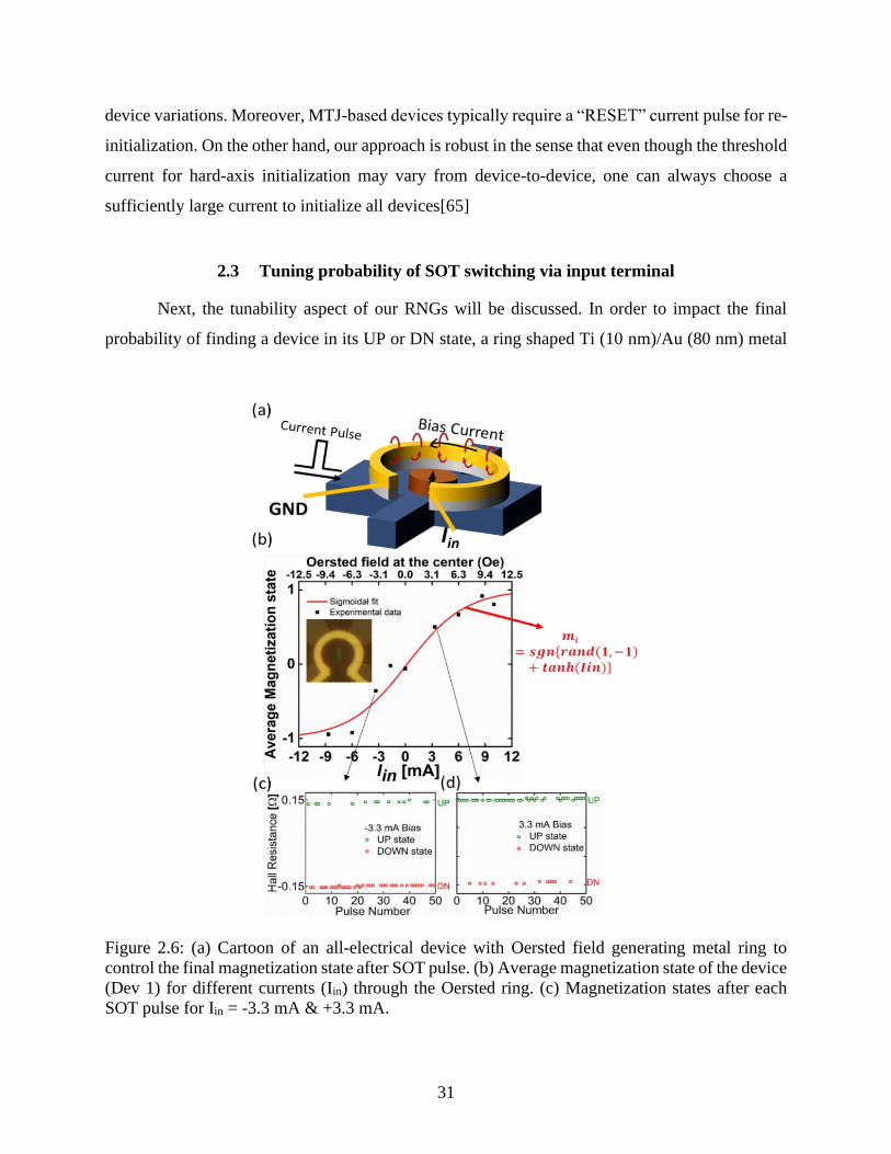
2.3 Tuning probability of SOT switching via input terminal
Next, the tunability aspect of our RNGs will be discussed. In order to impact the final
probability of finding a device in its UP or DN state, a ring shaped Ti (10 nm)/Au (80 nm) metal
Figure 2.6: (a) Cartoon of an all-electrical device with Oersted field generating metal ring to
control the final magnetization state after SOT pulse. (b) Average magnetization state of the device
(Dev 1) for different currents (Iin) through the Oersted ring. (c) Magnetization states after each
SOT pulse for Iin = -3.3 mA & +3.3 mA.
32
loop was designed around the nano-magnet as shown in Figure 2.6(a). This metal loop was isolated
from the underlying Hall bar by a 120nm thick SiO2 layer. Passing current through the loop was
employed to generate a symmetry breaking Oersted field, which allows tuning the probability of
the final magnetization state after releasing the SOT current. The out-of-plane Oersted field
generated at the location of the nano-magnet is approximately given by 𝜇0𝐼
2𝑟⁄ (𝑒𝑞. 1) and was
kept “on” during the SOT pulses. ~12 Oe field could be generated by passing 10 mA current
through the loop, which was sufficient to entirely pin the magnetization in the UP or DN state with
a ~100% probability. Figure 2.6(b) shows the average magnetization (averaging over either 72 or
51 pulses) as a function of the current applied to the loop (Iin), displaying the expected sigmoidal
shaped curve taking into account more than 600 measured data. Figure 2.6(c) and (d) show
exemplary AHE states measured at Iin of -3.3 mA and +3.3 mA, which resulted in the respective
data points in the main plot. To our knowledge, this is the first demonstration of a current
controlled spin device with tunable stochasticity and input-output isolation! To complement the
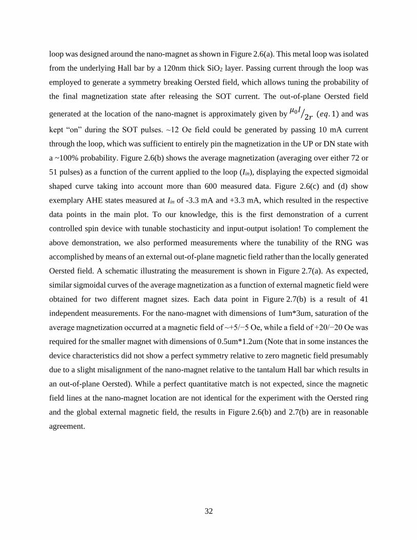
above demonstration, we also performed measurements where the tunability of the RNG was
accomplished by means of an external out-of-plane magnetic field rather than the locally generated
Oersted field. A schematic illustrating the measurement is shown in Figure 2.7(a). As expected,
similar sigmoidal curves of the average magnetization as a function of external magnetic field were
obtained for two different magnet sizes. Each data point in Figure 2.7(b) is a result of 41
independent measurements. For the nano-magnet with dimensions of 1um*3um, saturation of the
average magnetization occurred at a magnetic field of ~+5/−5 Oe, while a field of +20/−20 Oe was
required for the smaller magnet with dimensions of 0.5um*1.2um (Note that in some instances the
device characteristics did not show a perfect symmetry relative to zero magnetic field presumably
due to a slight misalignment of the nano-magnet relative to the tantalum Hall bar which results in
an out-of-plane Oersted). While a perfect quantitative match is not expected, since the magnetic
field lines at the nano-magnet location are not identical for the experiment with the Oersted ring
and the global external magnetic field, the results in Figure 2.6(b) and 2.7(b) are in reasonable
agreement.
33
To evaluate these findings, time-resolved simulations of mono-domain nano-magnets
using stochastic Landau-Lifshitz-Gilbert (sLLG) equation have been performed. Even though for
the magnet sizes used in the experiments, the sLLG assumptions, e.g. mono-domain behavior and
abrupt “input current turn-of ” do not strictly apply, the simulations provide valuable insights into
how the sigmoid curve gets effected by magnetic properties such as volume (V), magnetization
moment (Ms), and perpendicular magnetic anisotropic field (Hk). As in the experiment, a spin-
current pulse is applied for a certain time (dashed red line in Figure 2.7(c)) to drive the magnet
into its in-plane hard axis, while a small symmetry. breaking out-of-plane magnetic field is
simultaneously applied (green dashed line in Figure 2.7(c)). Figure 2.7(c) shows the dynamic
response of the nano-magnet’s z-component of the magnetization, mz, before and after the spin-
Figure 2.7: (a) Experimental set-up to measure average magnetization under
external magnetic field (Hext). (b) Average magnetization state of the device under
Hext -impact for two different magnet sizes. (c) sLLG simulations showing the
magnetization dynamics. (d) sLLG simulation results for magnets of sizes as
shown in (b).
34
current pulse has been removed. As apparent from the black solid and dashed line, different
simulation runs do indeed show that for the same conditions – in terms of symmetry breaking
magnetic field – the magnet can settle in the UP or DN state after initially having its magnetization
in-plane. However, as shown in Figure 2.7(d) the probability depends critically on the exact Hext-
value. Parameters used in the simulation are Ms=1000 emu/cc, Hk=200 mT, nano-magnet thickness
(t)=1nm and lateral sizes as shown in the figure legend. Each data point in Figure 2.7(d) represents
an average of 200 sLLG simulation runs. Consistent with the experimental findings, smaller nano-
magnets require a higher magnetic field to reach the condition that the magnet pins with a 100%
probability to one of its two states (UP or DN).
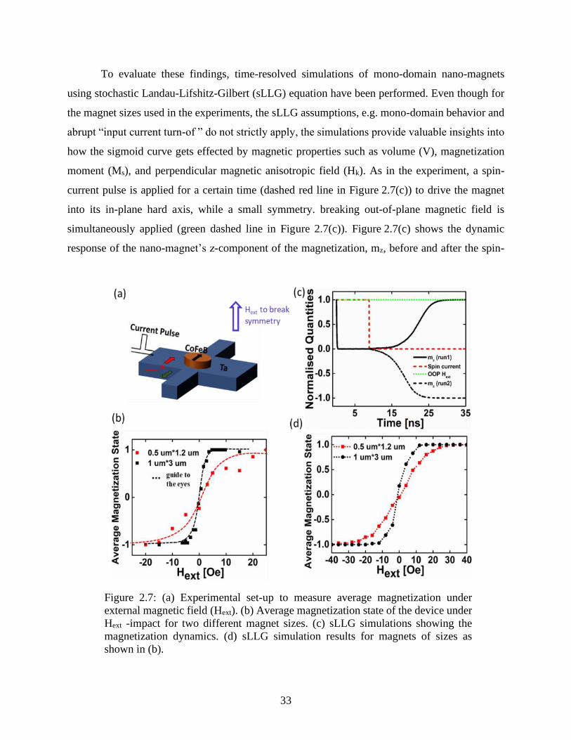
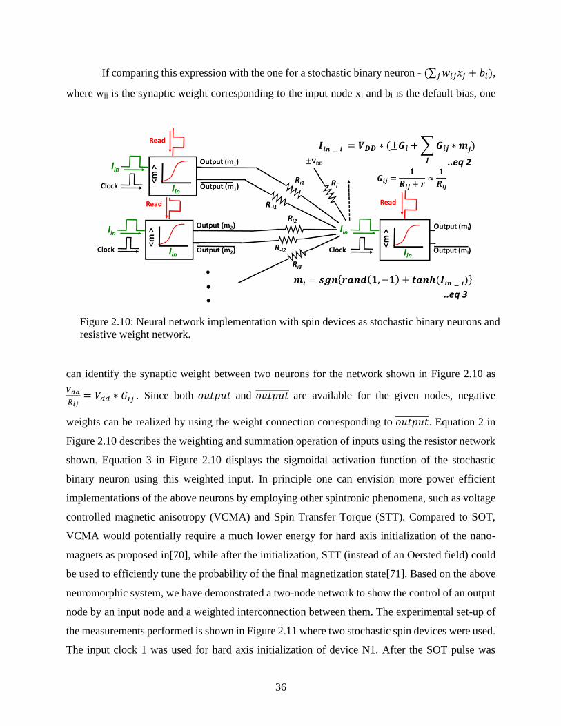
2.4 Directed network for neuromorphic computing
Stochastic spin devices demonstrated above can be employed as stochastic binary neurons
to be interconnected to form a neural network – similar to the ones proposed in ref. [70],[71],[72],
with its nodal representation shown in in Figure 2.9. In such a network, each node (one spin device)
will exhibit a sigmoidal activation function with inputs (in our case provided through the Oersted
ring) from the nodes of previous layers as shown in Figure 2.10. Layers will be updated
sequentially. Preferably, the magnetization state of the given node will be read using a magnetic
tunnel junction (MTJ) in series with two inverters as shown in the top of Figure 2.8. While the
Figure 2.8: (a) Two stochastic spin devices as described in the text used as binary stochastic
neurons. (b) Electrical inputs to the stochastic device, i.e. clock, Iin and READ.
35
READ operation can also be performed using AHE, as we will demonstrate in the following
experiment, it does require voltage amplification due to the relatively low achievable voltage
amplitude. Two inverters in series (see Figure 2.8 top) provide 𝑜𝑢𝑡𝑝𝑢𝑡 and 𝑜𝑢𝑡𝑝𝑢𝑡, which are
both required to realize positive and negative weights in the network. Electrical inputs, i.e. clock,
Iin and READ of the given node were applied according to Figure 2.8(b). The clock (in our case
an SOT pulse) is used to drive nodes (nano-magnets) into their metastable states in the given layer.
During the SOT pulse, outputs from previous layers weighted by a resistance network (synaptic
weights) are provided to the metal loops of the nodes in the current layer as an input. The input
current from node “j” of the previous layer to node “i” of the next layer, connected through the
resistance 𝑅𝑖𝑗 is defined by
𝐼𝑖𝑛−𝑖𝑗 =𝑚𝑗∗𝑉𝑑𝑑
𝑅𝑖𝑗+𝑟 ,
where 𝑟 is the resistance of Oersted ring and 𝑚𝑗 is the magnetization state of node j (+1 or
-1). For the case of a low resistance Oersted ring (𝑟) as in our experiment, this input current can
be approximated as
𝐼𝑖𝑛−𝑖𝑗 ≈𝑚𝑗∗𝑉𝑑𝑑
𝑅𝑖𝑗.
Input currents from multiple nodes “j” will be added at the Oersted ring of node “i”
providing a total input current of
𝐼𝑖𝑛−𝑖 = ∑𝑉𝑑𝑑∗𝑚𝑗
𝑅𝑖𝑗𝑗 .
Figure 2.9: Nodal representation of the neural network.
36
If comparing this expression with the one for a stochastic binary neuron - (∑ 𝑤𝑖𝑗𝑥𝑗 + 𝑏𝑖)𝑗 ,
where wjj is the synaptic weight corresponding to the input node xj and bi is the default bias, one
can identify the synaptic weight between two neurons for the network shown in Figure 2.10 as
𝑉𝑑𝑑
𝑅𝑖𝑗= 𝑉𝑑𝑑 ∗ 𝐺𝑖𝑗 . Since both 𝑜𝑢𝑡𝑝𝑢𝑡 and 𝑜𝑢𝑡𝑝𝑢𝑡 are available for the given nodes, negative
weights can be realized by using the weight connection corresponding to 𝑜𝑢𝑡𝑝𝑢𝑡. Equation 2 in
Figure 2.10 describes the weighting and summation operation of inputs using the resistor network
shown. Equation 3 in Figure 2.10 displays the sigmoidal activation function of the stochastic
binary neuron using this weighted input. In principle one can envision more power efficient
implementations of the above neurons by employing other spintronic phenomena, such as voltage
controlled magnetic anisotropy (VCMA) and Spin Transfer Torque (STT). Compared to SOT,
VCMA would potentially require a much lower energy for hard axis initialization of the nano-
magnets as proposed in[70], while after the initialization, STT (instead of an Oersted field) could
be used to efficiently tune the probability of the final magnetization state[71]. Based on the above
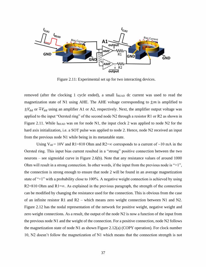
neuromorphic system, we have demonstrated a two-node network to show the control of an output
node by an input node and a weighted interconnection between them. The experimental set-up of
the measurements performed is shown in Figure 2.11 where two stochastic spin devices were used.
The input clock 1 was used for hard axis initialization of device N1. After the SOT pulse was
Figure 2.10: Neural network implementation with spin devices as stochastic binary neurons and
resistive weight network.
37
removed (after the clocking 1 cycle ended), a small IREAD dc current was used to read the
magnetization state of N1 using AHE. The AHE voltage corresponding to ±𝑚 is amplified to
±𝑉𝑑𝑑 or ∓𝑉𝑑𝑑 using an amplifier A1 or A2, respectively. Next, the amplifier output voltage was
applied to the input “Oersted ring” of the second node N2 through a resistor R1 or R2 as shown in
Figure 2.11. While IREAD was on for node N1, the input clock 2 was applied to node N2 for the
hard axis initialization, i.e. a SOT pulse was applied to node 2. Hence, node N2 received an input
from the previous node N1 while being in its metastable state.
Using Vdd = 10V and R1=810 Ohm and R2=∞ corresponds to a current of ~10 mA in the
Oersted ring. This input bias current resulted in a “strong” positive connection between the two
neurons – see sigmoidal curve in Figure 2.6(b). Note that any resistance values of around 1000
Ohm will result in a strong connection. In other words, if the input from the previous node is “+1”,
the connection is strong enough to ensure that node 2 will be found in an average magnetization
state of “+1” with a probability close to 100%. A negative weight connection is achieved by using
R2=810 Ohm and R1=∞. As explained in the previous paragraph, the strength of the connection
can be modified by changing the resistance used for the connection. This is obvious from the case
of an infinite resistor R1 and R2 – which means zero weight connection between N1 and N2.
Figure 2.12 has the nodal representation of the network for positive weight, negative weight and
zero weight connections. As a result, the output of the node N2 is now a function of the input from
the previous node N1 and the weight of the connection. For a positive connection, node N2 follows
the magnetization state of node N1 as shown Figure 2.12(a) (COPY operation). For clock number
10, N2 doesn’t follow the magnetization of N1 which means that the connection strength is not
Figure 2.11: Experimental set up for two interacting devices.
38
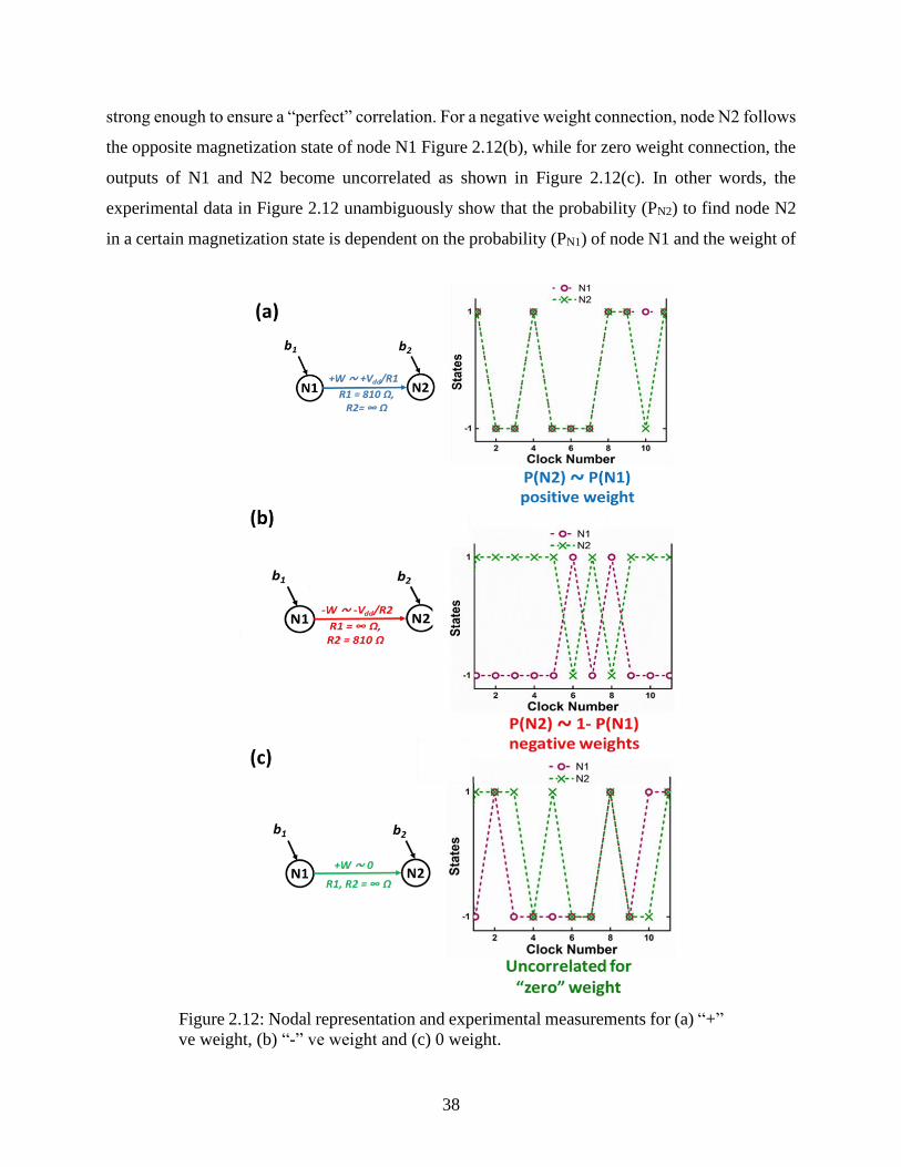
strong enough to ensure a “perfect” correlation. For a negative weight connection, node N2 follows
the opposite magnetization state of node N1 Figure 2.12(b), while for zero weight connection, the
outputs of N1 and N2 become uncorrelated as shown in Figure 2.12(c). In other words, the
experimental data in Figure 2.12 unambiguously show that the probability (PN2) to find node N2
in a certain magnetization state is dependent on the probability (PN1) of node N1 and the weight of
Figure 2.12: Nodal representation and experimental measurements for (a) “+”
ve weight, (b) “-” ve weight and (c) 0 weight.
39
the connection. PN2 is approximately either PN1 or 1 - PN1, depending on whether a strong positive
or negative weighted connection is used.
Here we have experimentally demonstrated a new type of stochastic spin devices, which
may become the building block for probabilistic computing. The unique properties of our devices,
such as a current controlled probabilistic binary output state and input-output isolation can be
exploited to perform a weighted summation of multiple input nodes like in stochastic binary
neurons. Using these stochastic devices, we have demonstrated a two-node directed network in
which the probability of the output node is a function of the input node and the weighted
connection between them. This experimental demonstration shows the potential of stochastic spin
devices as building blocks for directed networks with probabilistic outcomes such as Neural
networks and Bayesian networks.
40
SPIN-ORBIT TORQUE CONTROLLED LOW BARRIER MTJ AS A P-
BIT
© [2019] IEEE. Reprinted, with permission, from[73]: Ostwal Vaibhav, Appenzeller Joerg, "
Spin–Orbit Torque controlled magnetic tunnel junction with low thermal stability for tunable
random number generation." IEEE MAGNETICS LETTERS, Volume 10 (2019) 4503305.
In the previous chapter, we demonstrated probabilistic bit using hard axis initialization of
stable/high barrier nanomagnet. However, to generate each bit of random numbers, current pulses
to generate spin-torque and oersted field are required both of which are energy consuming
processes. In this chapter, we have experimentally demonstrated that spin-torque control of low-
barrier MTJ with device-structure similar to the one used in SOT-MRAM, is an energy efficient
and compact way to implement p-bit. In this device, low barrier in-plane MTJ shows random
telegraphic “hopping” between <+m> and <-m> magnetization states in time domain. Furthermore,
spin orbit torque generated using charge current flowing through Tantalum controls the probability
of MTJ being in <+m> and <-m> state. This device naturally provides input-output isolation
required for implementation of p-bits due decoupled WRITE and READ path.
3.1 Experimental section
An MTJ stack of Ta/CoFeB/MgO/CoFeB/Ru/CoFe/ PtMn/Ru (Figure 3.1(a)) was sputtered
onto a Si/SiO2 substrate using the Singulus Tool at SUNY ALBANY, where the CoFeB/Ru/CoFe
stack acts as a synthetic anti ferromagnetic (SAF) fixed layer, while PtMn is an antiferromagnetic
layer coupled to the SAF by means of exchange interaction. This stack is similar to the magnetic
stack used in STT-MTJs with exchange coupled SAF as fixed layer[20][21], with the difference,
however, that for our SOT-MTJs, the free layer CoFeB is located at the bottom of the stack, with
a 5 nm Ta layer underneath[22]. MTJs were pattered using a two-step e-beam lithography approach
and Ar ion-milling. In the 1st lithography step, the bottom electrode was patterned by etching down
to the substrate, while in the second lithography step, the MTJ metal pillar was defined by etching
until the bottom Ta layer was reached. The width and length of the Ta-channel are around 3 um
41
and 12 um respectively. Elliptical MTJs were patterned such that their easy axis is aligned
perpendicular to the current flow direction in the Ta underlayer to ensure that no symmetry
breaking magnetic field was required for SOT switching [23][24]. 90 nm of SiOx is used to
electrically isolate the top and the bottom contact of the MTJs. Finally, contacts were formed using
a lift-off process. MTJs were annealed at 300o C for an hour in a low-pressure Helium environment
in the presence of an in-plane magnetic field of 1 T collinear with easy axis of the MTJs. DC
current pulses or constant DC currents are used for SOT control of the MTJs with a measurement
set-up as shown in Figure 3.2(b). Tunneling Magneto Resistance (TMR) was measured directly
across the MTJ using an AC current of 2 µA at a frequency of 497 Hz employing lock-in technique
with time constants of 10 ms as shown in Figure 3.2(b).
Figure 3.1: (a) Material stack for our SOT-MTJ. (b) Schematic of SOT controlled
MTJ. (c) Scanning Electron Microscope (SEM) image of the MTJ and (d) major
loop for TMR vs. magnetic field (sweep rate = 480 Oe/min) of device 1. Copyright
© [2019] IEEE.
42
3.2 SOT switching of a thermally stable MTJ (device 1)
TMR vs. B-field major and minor loops of a thermally stable MTJ (device 1) (size~260*400
nm2 shown in Figure 3.1(c)) are shown in Figure 3.1(d) and 3.2 (b). Information about the field
sweep rate is provided in the figure caption. The minor loop for this device size exhibits an offset
of ~4 Oe. As apparent from the major loop, the MTJ gradually settles to the P state at magnetic
fields of around 1000 Oe due to the exchange coupled SAF switching, which is similar to STT-
MTJs with exchange coupled SAF layer[74]. Note that our MTJs exhibit relatively low TMR and
resistance-area products due to unintentional side wall metal re-deposition during the etching of our
MTJ pillars[75]. This side-wall metal re-deposition around the MTJ structures shunts the current
from flowing through the tunneling barrier and thus reduces the TMR signal.
Figure 3.2: (a) MTJ measurement set‐up for SOT switching. (b) Minor loop and (c) SOT
switching of stable MTJ (device 1) with quasi‐static current pulses (50 us wide) showing AP to P
switching for positive and P to AP switching for negative current pulses. Copyright © [2019]
IEEE.
43
Next, we used the GSHE in Ta to switch the magnetization of the free CoFeB magnetic layer
of the MTJ by passing quasi-static current pulses of 50 us in width through the Ta bottom layer.
Figure 3.2(c) shows GSHE current switching in the presence of an in-plane field of 4 Oe to
compensate for the small offset observed in the minor B-field loop. The current density is calculated
assuming that all current is passing through the 5 nm thick Ta with a channel width of 3 um. In the
measurement set-up, positive currents will generate spins in the -x direction and hence a low-
resistance parallel (P) state will be preferred by the system. Note that positive current pulses will
create positive Oersted fields, and these Oersted fields will try to switch the MTJ to its high-
resistance anti-parallel (AP) state. Hence, Oersted fields due to the applied current pulses can be
excluded as the reason for the observed MTJ switching. In other words, the polarity of the switching
in our experiment is consistent with the expected GSHE effect stemming from the current through
Ta. For AP to P switching, the current density required is around 3.5*107 A/cm2, while P to AP
switching requires a current density of around 4.5*107 A/cm2. To evaluate these numbers, we are
calculating the intrinsic critical current density required for GSHE switching according to [76]:
𝐽𝑐0 = (2𝑞
ℏ)𝜇0𝑀𝑠𝑡𝛼(𝐻𝑘
𝑖𝑛−𝑝𝑙𝑎𝑛𝑒 +𝑀𝑠
2)
1
Θ𝑆𝐻𝐸 …equation (1)
where 𝑀𝑠 is the saturation magnetization moment (≈1100 emu/cc) [63], 𝑡 is the thickness of
the magnet (1.5 nm), 𝛼 is the damping constant (0.01)[77], 𝐻𝑘𝑖𝑛−𝑝𝑙𝑎𝑛𝑒
is the in-plane anisotropy
field and Θ𝑆𝐻𝐸 is the spin Hall angle of Ta (≈0.1)[78]. For the in-plane magnet, the 𝐻𝑘𝑖𝑛−𝑝𝑙𝑎𝑛𝑒 term
can be neglected compared to 𝑀𝑠
2 (especially for MTJs with low aspect ratio as used in our
experiments). From these numbers we obtain 𝐽𝑐0 = 3.46 ∗ 107 𝐴
𝑐𝑚2 from eq. (1). Considering the
quasi-static (pulsed) switching we employed in our experiments, the critical current 𝐽𝑐 can be
calculated using the standard model for thermally activated switching [75] [76]:
𝐽𝑐 = 𝐽𝑐0 [1 −𝑘𝐵𝑇
𝐸𝑏ln
𝜏
𝜏0] ….equation (2)
where 𝜏0 is the attempt time (≈1ns) and 𝜏 is the pulse width of the GSHE current used (50
us). For stable MTJs assuming 𝐸𝑏
𝑘𝐵𝑇= 40, 𝐽𝑐 is approximately 0.75*𝐽𝑐0 = 2.58 ∗ 107 𝐴
𝑐𝑚2. This
value is in good agreement with our experimental findings, considering that any Oersted fields will
oppose the SOT switching. We also note that these switching current densities are similar to those
previously reported for in-plane MTJs[63][79].
44
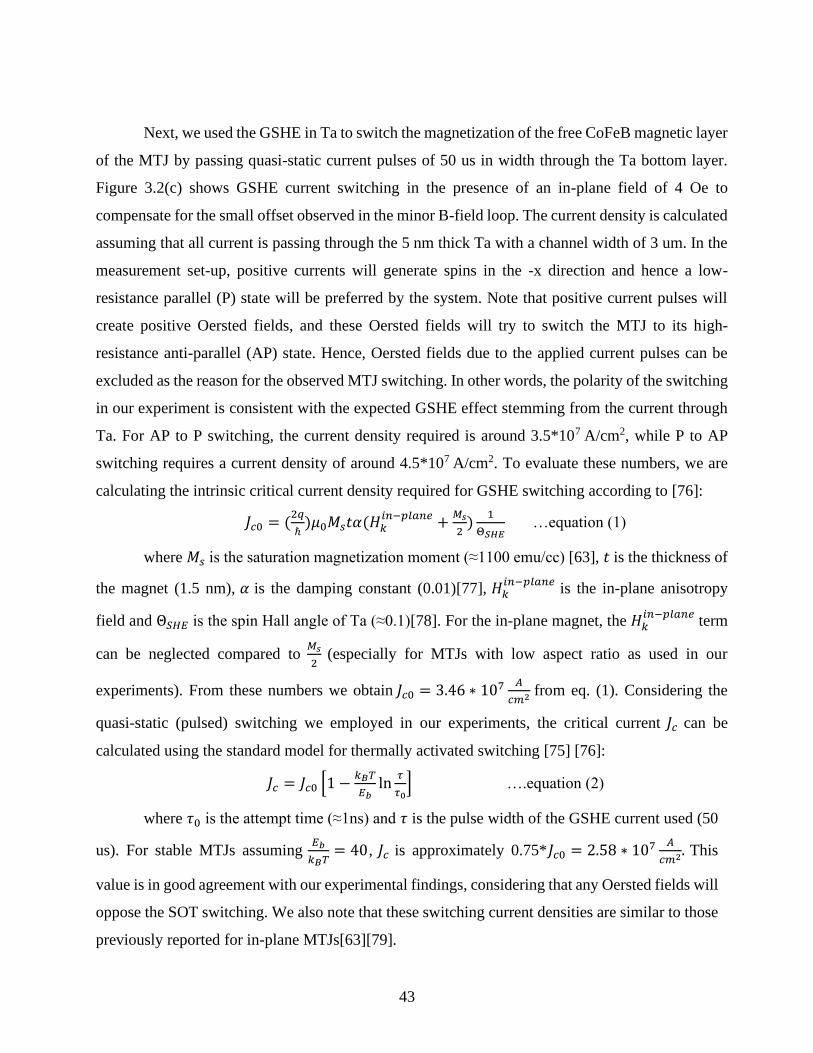
3.3 SOT control of MTJ with low thermal stability (device 2)
Having demonstrated GSHE switching in thermally stable MTJs, we will next discuss
similar measurements performed on a second type of MTJ, which has low thermal stability. The
size of this MTJ is around 160*260 nm2 as apparent from the SEM shown in the Figure 3.3(a), and
its smaller size is responsible for the different behavior if compared to device 1. During a slow
magnetic field sweep near the minor loop this MTJ toggles between two states (AP and P),
exhibiting telegraphic behavior as shown in Figure 3.3(a). The offset in the minor loop for this
Figure 3.3: (a) Minor B-field loop (sweep rate= 0.4 Oe/min) for a MTJ with low thermal stability
(device 2) with the SEM image. When the B-field is swept slowly during the minor loop
measurement, the MTJ with low thermal stability shows random fluctuations between the AP and
P states. The minor loop offset is around 14 Oe for this device size. (b) Zoom-in minor loop at Hext
of 14 Oe (to compensate for the minor loop offset at zero magnetic field) showing telegraphic
switching between the AP and the P state (red curve) and digitized data (black curve) to infer the
magnetization state of the free layer. Copyright © [2019] IEEE.
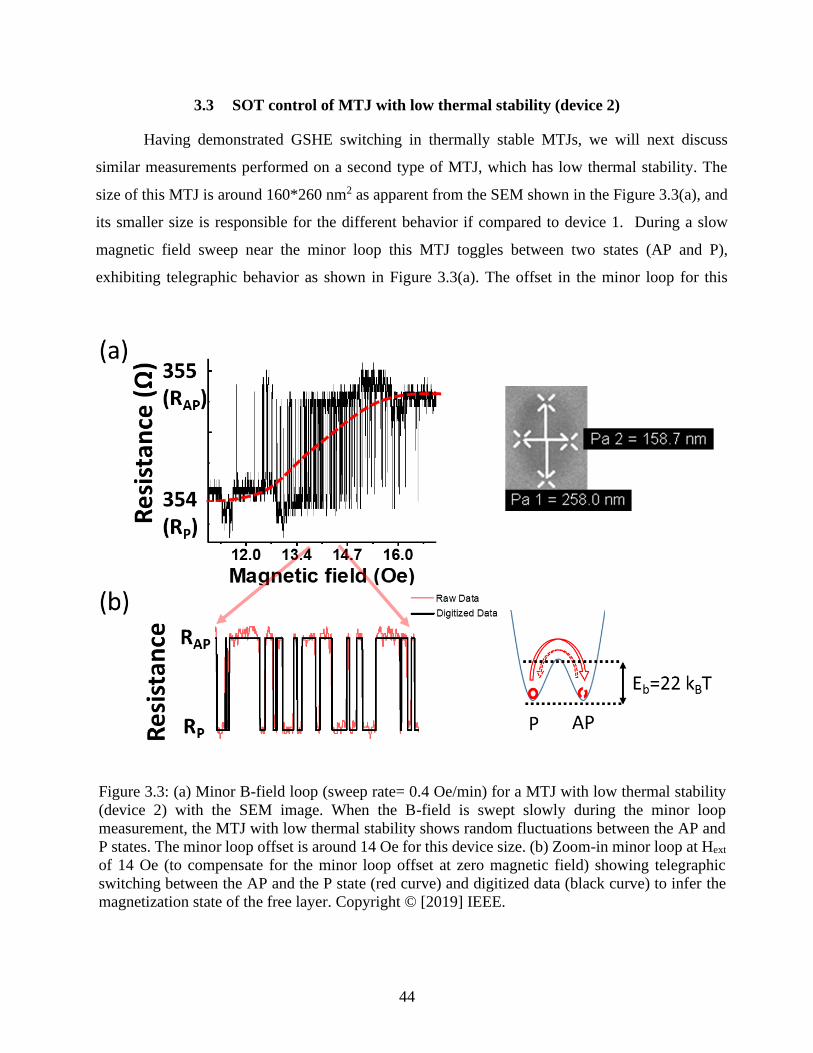
45
device size is around 14 Oe, which is a result of stray fields from the SAF or Neel dipolar orange-
peel effect [77]. Figure 3.3(b) shows a zoom-in image of the minor loop at around 14 Oe with two
distinct resistance states AP and P respectively. Note that the black line is a digitized version of the
raw data. The sweep rate used for the minor loop measurement was 0.4 Oe/min. The MTJ under
investigation is in its P state for magnetic fields < 10 Oe and in its AP state for fields > 17 Oe.
Random telegraphic switching between the AP and P state is expected to follow a Poisson
distribution with respect to the dwell time, i.e. the time the MTJ stays in either of the two states and
should exponentially decrease. To perform such a dwell time analysis, the MTJ resistance was
characterized for over an hour at an external field of 14 Oe. Next, the magnetoresistance data are
Figure 3.4: (a) Magnetization states obtained during near 1hr measurements at
Hext=14 Oe. (b) Obtained number of counts vs lifetime for AP (Red) and P
(Green) states in semilog plot using measurement in (a). At Hext = 14 Oe, sMTJ
has equal characteristic lifetime for AP and P states. Copyright © [2019] IEEE.
46
digitized to +1 and 0 (Figure 3.4(a)) by applying a proper threshold operation to the TMR data as
displayed in Figure 3.3(b). At an external field of 14 Oe, the probability for the MTJ to be in its AP
versus P state is found to be ~50 %. Figure 3.4(b) displays the number of counts for a dwell time in
a semi-logarithmic plot. From the linear fit to this plot a characteristic lifetime to find the MTJ in
its P (𝜏𝑃) and AP (𝜏𝐴𝑃) state of around 3 sec is found for both 𝜏𝑃 and 𝜏𝐴𝑃. Using this experimental
finding, an energy barrier (Δ𝑖𝑛−𝑝𝑙𝑎𝑛𝑒) of ~22 kBT can be determined from 𝜏 = 𝜏0𝑒𝑥𝑝 [Δ𝑖𝑛−𝑝𝑙𝑎𝑛𝑒
𝑘𝐵𝑇].
We also observed a clear temperature dependence of switching rates in our device as shown in
Figure 3.5(a), (b) and (c) below. The average switching times of the device at 290 K, 300 K and 320
K are approximately 4 sec, 3 sec and 1.2 sec respectively.
Next, tests from the National Institute of Standards and Technology (NIST) Statistical Test
Suit (STS) [68] are performed based on the above experimental magnetization data that was used
for the dwell time analysis in Figure 3.4(b) . Since, 𝜏𝑃 = 𝜏𝐴𝑃 = 3 sec, magnetization states are read
after each 6 sec (2𝜏) for the NIST tests. Note that some of the tests in the suit are not applicable due
to the limited sample size (~650 samples) in our case. Table 3.1 shows the test name and the
respective p-values obtained for the test on the raw data and after performing an XOR operation
used to increase the Shannon entropy [80] and hence the randomness. If the obtained p-value is
greater than 0.01, the sample is considered to have passed the test. As shown in table 2, already the
raw data obtained from the magnetization states of our stochastic, i.e. MTJ with low thermal stability
passes all the test performed (shown in green) except one (shown in red), while data after XOR
Figure 3.5: (a) Magnetization states obtained at Hext =14 Oe for temperature of (a) 290 K (b) 300
K and (c) 320 K.
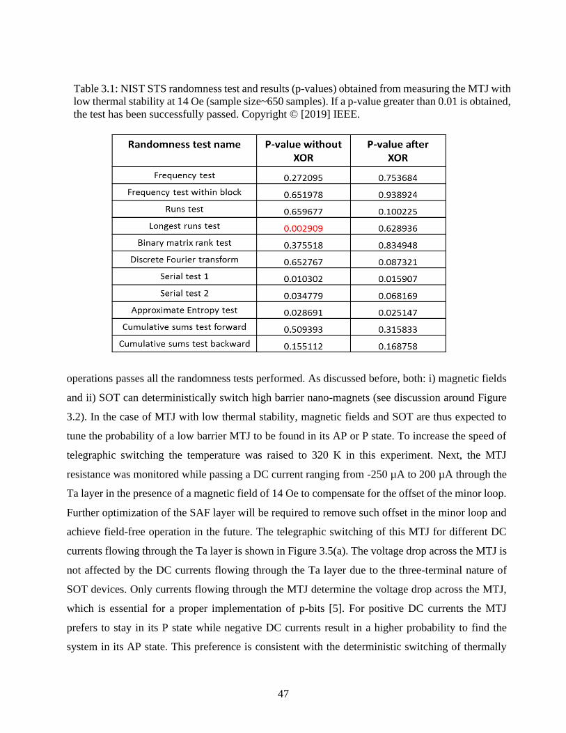
47
operations passes all the randomness tests performed. As discussed before, both: i) magnetic fields
and ii) SOT can deterministically switch high barrier nano-magnets (see discussion around Figure
3.2). In the case of MTJ with low thermal stability, magnetic fields and SOT are thus expected to
tune the probability of a low barrier MTJ to be found in its AP or P state. To increase the speed of
telegraphic switching the temperature was raised to 320 K in this experiment. Next, the MTJ
resistance was monitored while passing a DC current ranging from -250 µA to 200 µA through the
Ta layer in the presence of a magnetic field of 14 Oe to compensate for the offset of the minor loop.
Further optimization of the SAF layer will be required to remove such offset in the minor loop and
achieve field-free operation in the future. The telegraphic switching of this MTJ for different DC
currents flowing through the Ta layer is shown in Figure 3.5(a). The voltage drop across the MTJ is
not affected by the DC currents flowing through the Ta layer due to the three-terminal nature of
SOT devices. Only currents flowing through the MTJ determine the voltage drop across the MTJ,
which is essential for a proper implementation of p-bits [5]. For positive DC currents the MTJ
prefers to stay in its P state while negative DC currents result in a higher probability to find the
system in its AP state. This preference is consistent with the deterministic switching of thermally
Table 3.1: NIST STS randomness test and results (p-values) obtained from measuring the MTJ with
low thermal stability at 14 Oe (sample size~650 samples). If a p-value greater than 0.01 is obtained,
the test has been successfully passed. Copyright © [2019] IEEE.
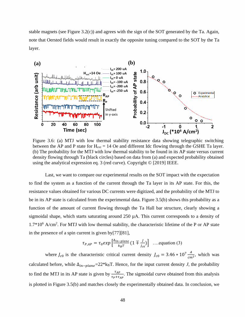
48
stable magnets (see Figure 3.2(c)) and agrees with the sign of the SOT generated by the Ta. Again,
note that Oersted fields would result in exactly the opposite tuning compared to the SOT by the Ta
layer.
Last, we want to compare our experimental results on the SOT impact with the expectation
to find the system as a function of the current through the Ta layer in its AP state. For this, the
resistance values obtained for various DC currents were digitized, and the probability of the MTJ to
be in its AP state is calculated from the experimental data. Figure 3.5(b) shows this probability as a
function of the amount of current flowing through the Ta Hall bar structure, clearly showing a
sigmoidal shape, which starts saturating around 250 µA. This current corresponds to a density of
1.7*106 A/cm2. For MTJ with low thermal stability, the characteristic lifetime of the P or AP state
in the presence of a spin current is given by[77][81],
𝜏𝑃,𝐴𝑃 = 𝜏0𝑒𝑥𝑝 [Δ𝑖𝑛−𝑝𝑙𝑎𝑛𝑒
𝑘𝐵𝑇(1 ∓
𝐽
𝐽𝑐0)] ….equation (3)
where 𝐽𝑐0 is the characteristic critical current density 𝐽𝑐0 = 3.46 ∗ 107 𝐴
𝑐𝑚2 , which was
calculated before, while Δ𝑖𝑛−𝑝𝑙𝑎𝑛𝑒=22*kBT. Hence, for the input current density J, the probability
to find the MTJ in its AP state is given by 𝜏𝐴𝑃
𝜏𝑃+𝜏𝐴𝑃. The sigmoidal curve obtained from this analysis
is plotted in Figure 3.5(b) and matches closely the experimentally obtained data. In conclusion, we
(a) (b)
Figure 3.6: (a) MTJ with low thermal stability resistance data showing telegraphic switching
between the AP and P state for Hext = 14 Oe and different Idc flowing through the GSHE Ta layer.
(b) The probability for the MTJ with low thermal stability to be found in its AP state versus current
density flowing through Ta (black circles) based on data from (a) and expected probability obtained
using the analytical expression eq. 3 (red curve). Copyright © [2019] IEEE.

49
have successfully demonstrated that MTJs with low thermal stability are natural candidates as RNG,
while spin currents can be used in an efficient way to tune such low barrier MTJs and hence provide
a compact device that is capable to operate as a tunable RNG.
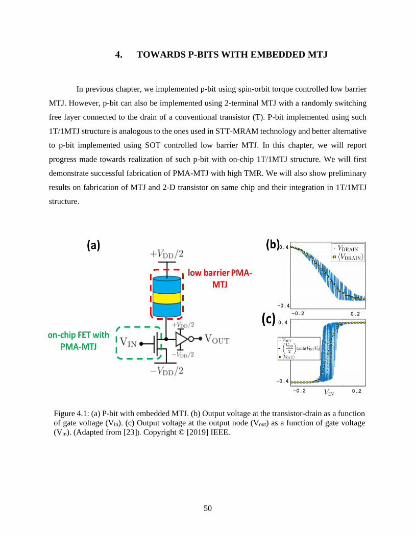
50
TOWARDS P-BITS WITH EMBEDDED MTJ
In previous chapter, we implemented p-bit using spin-orbit torque controlled low barrier
MTJ. However, p-bit can also be implemented using 2-terminal MTJ with a randomly switching
free layer connected to the drain of a conventional transistor (T). P-bit implemented using such
1T/1MTJ structure is analogous to the ones used in STT-MRAM technology and better alternative
to p-bit implemented using SOT controlled low barrier MTJ. In this chapter, we will report
progress made towards realization of such p-bit with on-chip 1T/1MTJ structure. We will first
demonstrate successful fabrication of PMA-MTJ with high TMR. We will also show preliminary
results on fabrication of MTJ and 2-D transistor on same chip and their integration in 1T/1MTJ
structure.
Figure 4.1: (a) P-bit with embedded MTJ. (b) Output voltage at the transistor-drain as a function
of gate voltage (Vin). (c) Output voltage at the output node (Vout) as a function of gate voltage
(Vin). (Adapted from [23]). Copyright © [2019] IEEE.
51
4.1 Introduction
One of the proposals for implementing p-bits consists of low barrier MTJ connected in
series with transistor as shown in Figure 4.1 (a) which is similar to the structures used in STT-
MRAM technology. In such structure, if conductance of transistor (NMOS) for Vin = 0 is similar
to the conductance of MTJ, fluctuations in magnetization of low barrier MTJ will be converted to
voltage fluctuations at the output (Vout). However, with Vin < 0, the transistor is OFF and Vout is
pinned to -Vdd/2 independent of the magnetization fluctuation of the MTJ. On the other hand, with
Vin > 0, the transistor is ON and Vout is pinned to +Vdd/2 independent of the magnetization
fluctuation of the MTJ. Overall, average of fluctuating Vout (<Vout>) is sigmoidal function of Vin
as shown in Figure 4.1 similar to a p-bit. To implement such p-bit, one requires low barrier MTJ
with good TMR so that voltage fluctuation at the Vdrain are large enough to be amplified by the
inverter. To achieve such MTJ, we will first show successful fabrication of nanoscale stable PMA-
MTJ with TMR > 60% and then study annealing recipe for PMA-MTJs as a tool to control it’s
magnetic anisotropy i.e. energy barrier. We also need on-chip transistor with conductance in ON
state (GON) to be much larger than average conductance of MTJ and conductance in OFF state
(GOFF) to be much smaller than average conductance of MTJ. In section 4.4, we will demonstrate
a 2-Dimentional transistor satisfying these conditions on same chip as PMA-MTJ. Essentially, in
this chapter we have successfully implemented all the building blocks required for p-bits with
embedded MTJs.
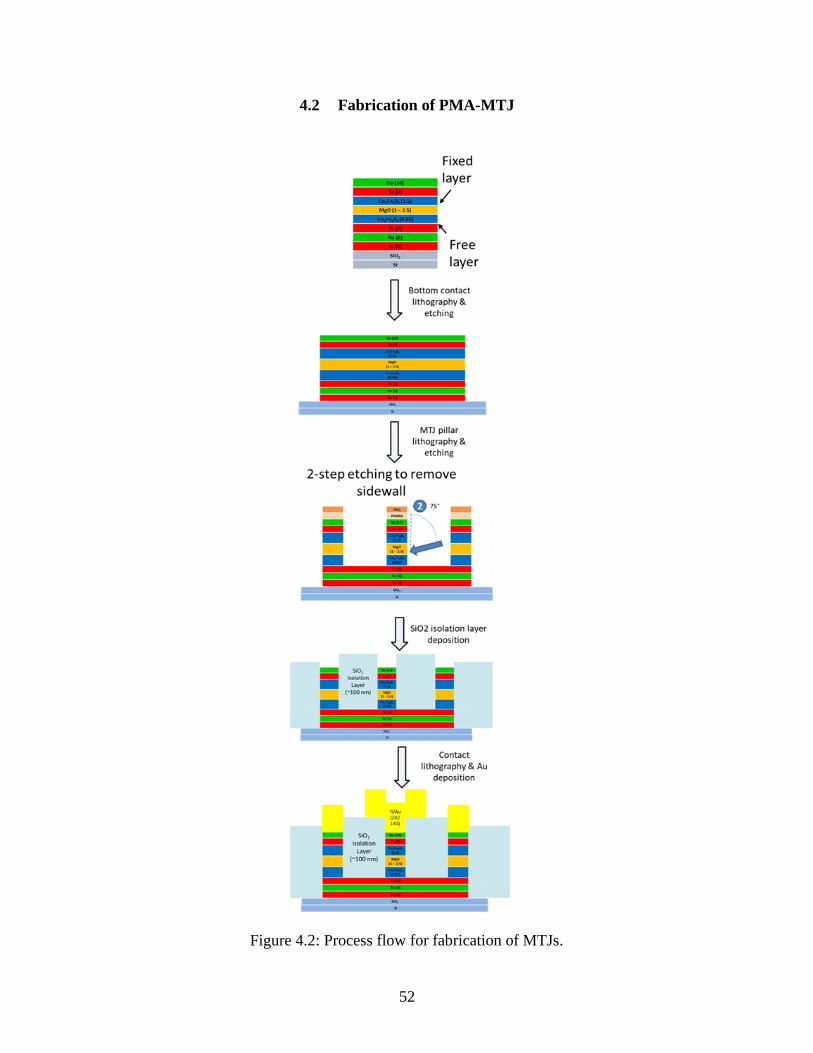
52
4.2 Fabrication of PMA-MTJ
Figure 4.2: Process flow for fabrication of MTJs.
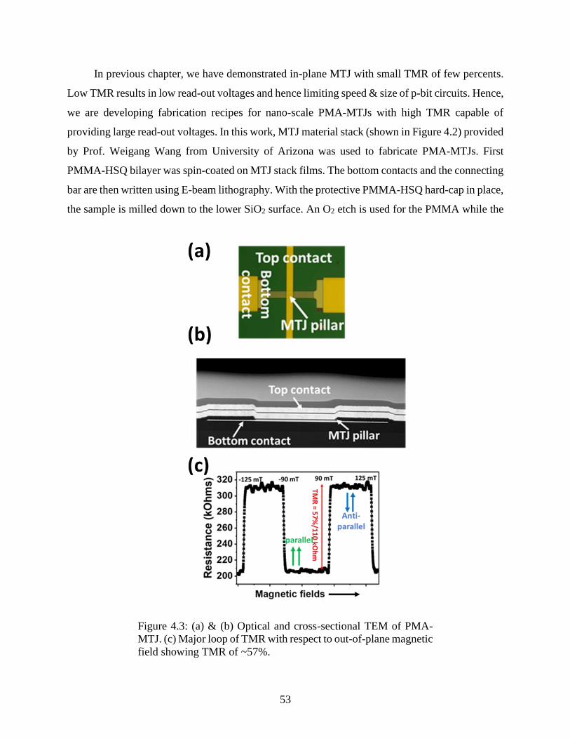
53
In previous chapter, we have demonstrated in-plane MTJ with small TMR of few percents.
Low TMR results in low read-out voltages and hence limiting speed & size of p-bit circuits. Hence,
we are developing fabrication recipes for nano-scale PMA-MTJs with high TMR capable of
providing large read-out voltages. In this work, MTJ material stack (shown in Figure 4.2) provided
by Prof. Weigang Wang from University of Arizona was used to fabricate PMA-MTJs. First
PMMA-HSQ bilayer was spin-coated on MTJ stack films. The bottom contacts and the connecting
bar are then written using E-beam lithography. With the protective PMMA-HSQ hard-cap in place,
the sample is milled down to the lower SiO2 surface. An O2 etch is used for the PMMA while the
Figure 4.3: (a) & (b) Optical and cross-sectional TEM of PMA-
MTJ. (c) Major loop of TMR with respect to out-of-plane magnetic
field showing TMR of ~57%.
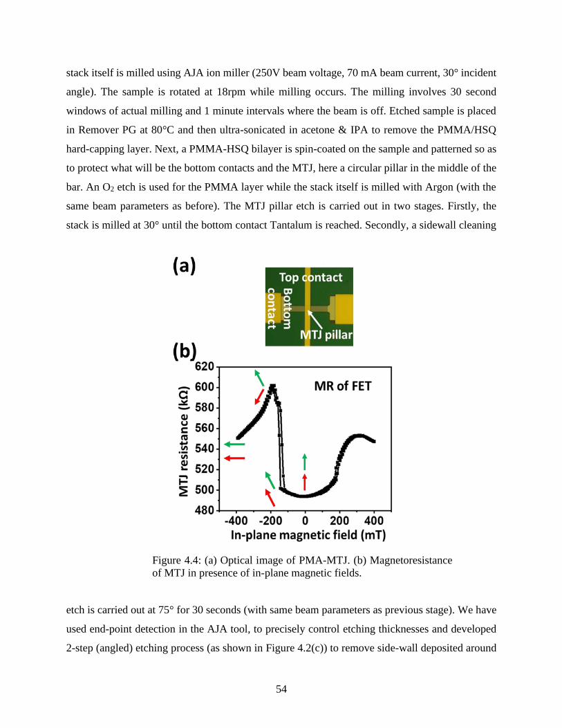
54
stack itself is milled using AJA ion miller (250V beam voltage, 70 mA beam current, 30° incident
angle). The sample is rotated at 18rpm while milling occurs. The milling involves 30 second
windows of actual milling and 1 minute intervals where the beam is off. Etched sample is placed
in Remover PG at 80°C and then ultra-sonicated in acetone & IPA to remove the PMMA/HSQ
hard-capping layer. Next, a PMMA-HSQ bilayer is spin-coated on the sample and patterned so as
to protect what will be the bottom contacts and the MTJ, here a circular pillar in the middle of the
bar. An O2 etch is used for the PMMA layer while the stack itself is milled with Argon (with the
same beam parameters as before). The MTJ pillar etch is carried out in two stages. Firstly, the
stack is milled at 30° until the bottom contact Tantalum is reached. Secondly, a sidewall cleaning
etch is carried out at 75° for 30 seconds (with same beam parameters as previous stage). We have
used end-point detection in the AJA tool, to precisely control etching thicknesses and developed
2-step (angled) etching process (as shown in Figure 4.2(c)) to remove side-wall deposited around
Figure 4.4: (a) Optical image of PMA-MTJ. (b) Magnetoresistance
of MTJ in presence of in-plane magnetic fields.
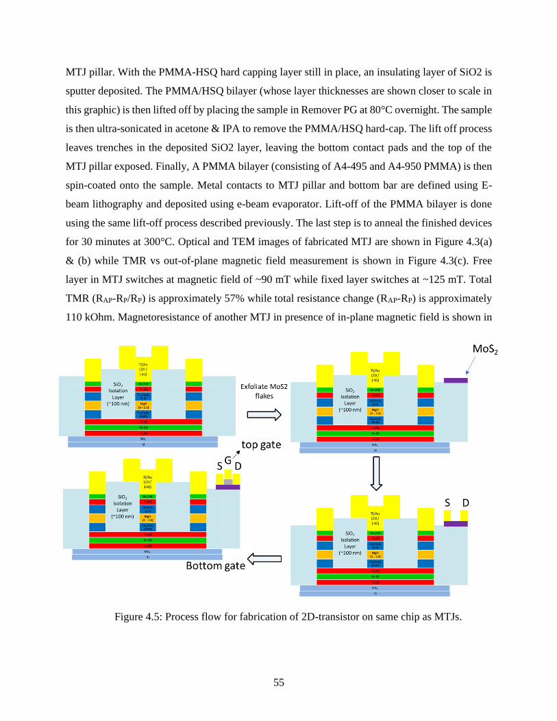
55
MTJ pillar. With the PMMA-HSQ hard capping layer still in place, an insulating layer of SiO2 is
sputter deposited. The PMMA/HSQ bilayer (whose layer thicknesses are shown closer to scale in
this graphic) is then lifted off by placing the sample in Remover PG at 80°C overnight. The sample
is then ultra-sonicated in acetone & IPA to remove the PMMA/HSQ hard-cap. The lift off process
leaves trenches in the deposited SiO2 layer, leaving the bottom contact pads and the top of the
MTJ pillar exposed. Finally, A PMMA bilayer (consisting of A4-495 and A4-950 PMMA) is then
spin-coated onto the sample. Metal contacts to MTJ pillar and bottom bar are defined using E-
beam lithography and deposited using e-beam evaporator. Lift-off of the PMMA bilayer is done
using the same lift-off process described previously. The last step is to anneal the finished devices
for 30 minutes at 300°C. Optical and TEM images of fabricated MTJ are shown in Figure 4.3(a)
& (b) while TMR vs out-of-plane magnetic field measurement is shown in Figure 4.3(c). Free
layer in MTJ switches at magnetic field of ~90 mT while fixed layer switches at ~125 mT. Total
TMR (RAP-RP/RP) is approximately 57% while total resistance change (RAP-RP) is approximately
110 kOhm. Magnetoresistance of another MTJ in presence of in-plane magnetic field is shown in
Figure 4.5: Process flow for fabrication of 2D-transistor on same chip as MTJs.
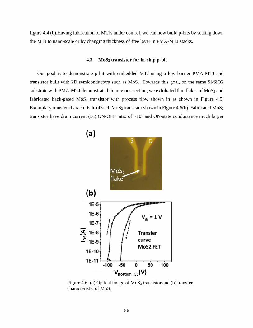
56
figure 4.4 (b).Having fabrication of MTJs under control, we can now build p-bits by scaling down
the MTJ to nano-scale or by changing thickness of free layer in PMA-MTJ stacks.
4.3 MoS2 transistor for in-chip p-bit
Our goal is to demonstrate p-bit with embedded MTJ using a low barrier PMA-MTJ and
transistor built with 2D semiconductors such as MoS2. Towards this goal, on the same Si/SiO2
substrate with PMA-MTJ demonstrated in previous section, we exfoliated thin flakes of MoS2 and
fabricated back-gated MoS2 transistor with process flow shown in as shown in Figure 4.5.
Exemplary transfer characteristic of such MoS2 transistor shown in Figure 4.6(b). Fabricated MoS2
transistor have drain current (Ids) ON-OFF ratio of ~106 and ON-state conductance much larger
Figure 4.6: (a) Optical image of MoS2 transistor and (b) transfer
characteristic of MoS2
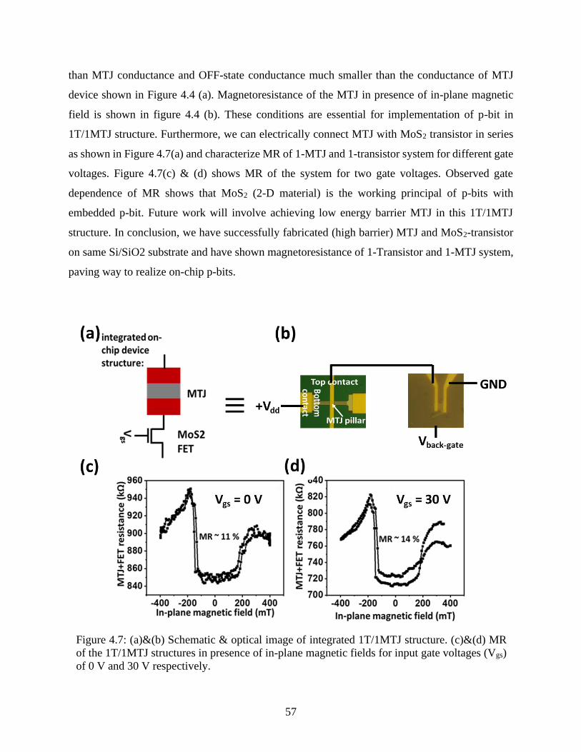
57
than MTJ conductance and OFF-state conductance much smaller than the conductance of MTJ
device shown in Figure 4.4 (a). Magnetoresistance of the MTJ in presence of in-plane magnetic
field is shown in figure 4.4 (b). These conditions are essential for implementation of p-bit in
1T/1MTJ structure. Furthermore, we can electrically connect MTJ with MoS2 transistor in series
as shown in Figure 4.7(a) and characterize MR of 1-MTJ and 1-transistor system for different gate
voltages. Figure 4.7(c) & (d) shows MR of the system for two gate voltages. Observed gate
dependence of MR shows that MoS2 (2-D material) is the working principal of p-bits with
embedded p-bit. Future work will involve achieving low energy barrier MTJ in this 1T/1MTJ
structure. In conclusion, we have successfully fabricated (high barrier) MTJ and MoS2-transistor
on same Si/SiO2 substrate and have shown magnetoresistance of 1-Transistor and 1-MTJ system,
paving way to realize on-chip p-bits.
Figure 4.7: (a)&(b) Schematic & optical image of integrated 1T/1MTJ structure. (c)&(d) MR
of the 1T/1MTJ structures in presence of in-plane magnetic fields for input gate voltages (Vgs)
of 0 V and 30 V respectively.
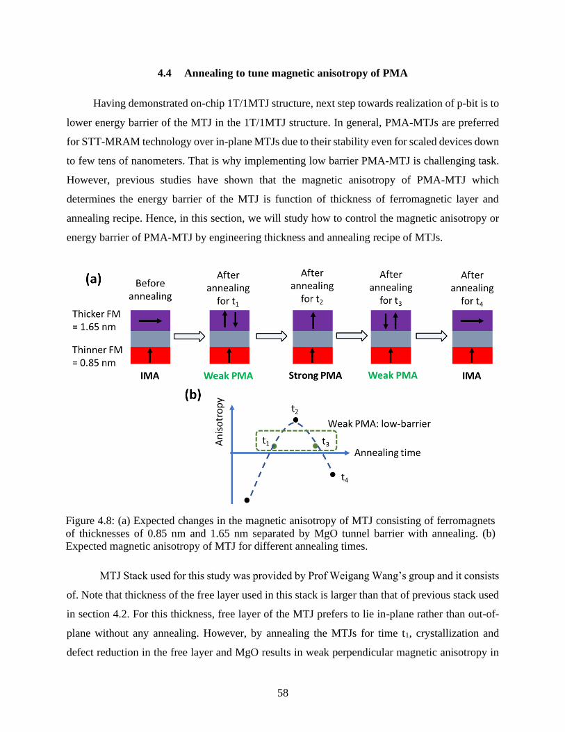
58
4.4 Annealing to tune magnetic anisotropy of PMA
Having demonstrated on-chip 1T/1MTJ structure, next step towards realization of p-bit is to
lower energy barrier of the MTJ in the 1T/1MTJ structure. In general, PMA-MTJs are preferred
for STT-MRAM technology over in-plane MTJs due to their stability even for scaled devices down
to few tens of nanometers. That is why implementing low barrier PMA-MTJ is challenging task.
However, previous studies have shown that the magnetic anisotropy of PMA-MTJ which
determines the energy barrier of the MTJ is function of thickness of ferromagnetic layer and
annealing recipe. Hence, in this section, we will study how to control the magnetic anisotropy or
energy barrier of PMA-MTJ by engineering thickness and annealing recipe of MTJs.
MTJ Stack used for this study was provided by Prof Weigang Wang’s group and it consists
of. Note that thickness of the free layer used in this stack is larger than that of previous stack used
in section 4.2. For this thickness, free layer of the MTJ prefers to lie in-plane rather than out-of-
plane without any annealing. However, by annealing the MTJs for time t1, crystallization and
defect reduction in the free layer and MgO results in weak perpendicular magnetic anisotropy in
Figure 4.8: (a) Expected changes in the magnetic anisotropy of MTJ consisting of ferromagnets
of thicknesses of 0.85 nm and 1.65 nm separated by MgO tunnel barrier with annealing. (b)
Expected magnetic anisotropy of MTJ for different annealing times.
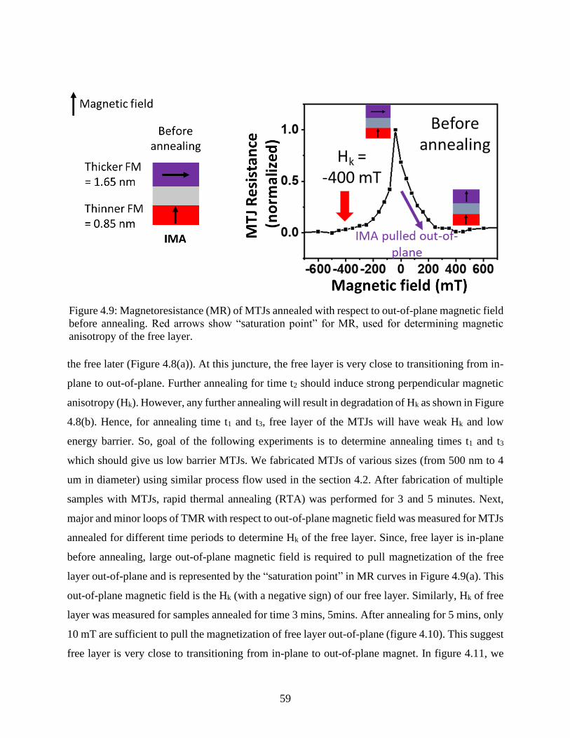
59
the free later (Figure 4.8(a)). At this juncture, the free layer is very close to transitioning from in-
plane to out-of-plane. Further annealing for time t2 should induce strong perpendicular magnetic
anisotropy (Hk). However, any further annealing will result in degradation of Hk as shown in Figure
4.8(b). Hence, for annealing time t1 and t3, free layer of the MTJs will have weak Hk and low
energy barrier. So, goal of the following experiments is to determine annealing times t1 and t3
which should give us low barrier MTJs. We fabricated MTJs of various sizes (from 500 nm to 4
um in diameter) using similar process flow used in the section 4.2. After fabrication of multiple
samples with MTJs, rapid thermal annealing (RTA) was performed for 3 and 5 minutes. Next,
major and minor loops of TMR with respect to out-of-plane magnetic field was measured for MTJs
annealed for different time periods to determine Hk of the free layer. Since, free layer is in-plane
before annealing, large out-of-plane magnetic field is required to pull magnetization of the free
layer out-of-plane and is represented by the “saturation point” in MR curves in Figure 4.9(a). This
out-of-plane magnetic field is the Hk (with a negative sign) of our free layer. Similarly, Hk of free
layer was measured for samples annealed for time 3 mins, 5mins. After annealing for 5 mins, only
10 mT are sufficient to pull the magnetization of free layer out-of-plane (figure 4.10). This suggest
free layer is very close to transitioning from in-plane to out-of-plane magnet. In figure 4.11, we
Figure 4.9: Magnetoresistance (MR) of MTJs annealed with respect to out-of-plane magnetic field
before annealing. Red arrows show “saturation point” for MR, used for determining magnetic
anisotropy of the free layer.
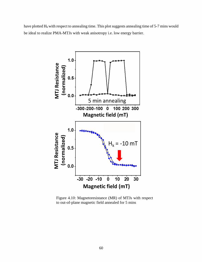
60
have plotted Hk with respect to annealing time. This plot suggests annealing time of 5-7 mins would
be ideal to realize PMA-MTJs with weak anisotropy i.e. low energy barrier.
Figure 4.10: Magnetoresistance (MR) of MTJs with respect
to out-of-plane magnetic field annealed for 5 mins
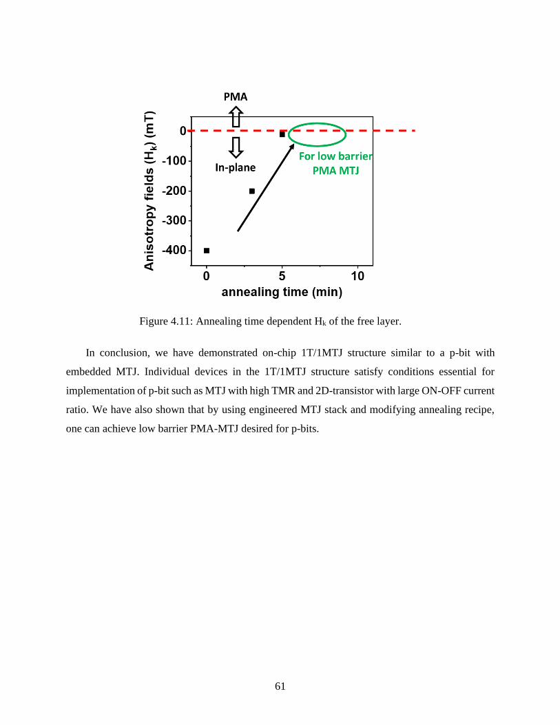
61
In conclusion, we have demonstrated on-chip 1T/1MTJ structure similar to a p-bit with
embedded MTJ. Individual devices in the 1T/1MTJ structure satisfy conditions essential for
implementation of p-bit such as MTJ with high TMR and 2D-transistor with large ON-OFF current
ratio. We have also shown that by using engineered MTJ stack and modifying annealing recipe,
one can achieve low barrier PMA-MTJ desired for p-bits.
Figure 4.11: Annealing time dependent Hk of the free layer.
62
COMPOUND SYNAPSE USING PROBABILISTIC SOT SWITCHING
Most of the material in this chapter has been reprinted from [29]: Ostwal, V., Zand, R., DeMara,
R., & Appenzeller, J. (2019). A Novel Compound Synapse Using Probabilistic Spin–Orbit-Torque
Switching for MTJ-Based Deep Neural Networks. IEEE Journal on Exploratory Solid-State
Computational Devices and Circuits, 5(2), 182-187. This article is distributed under a Creative
Commons Attribution CC BY license.
Applications of PSL requires networks of p-bits connected via weighted interconnects.
Hence, programmable non-volatile interconnects, similar to analog resistive cross-bar
architectures (synaptic networks) commonly used for neuromorphic computing are required for
realization of PSL. In this chapter, we will show analog-type synaptic behavior using stochastic
SOT switching of stable/high-barrier nanomagnets paving a way to realize p-bit networks solely
with MTJs integrated with CMOS devices. We utilize concept of compound synapses that consist
of an ensemble of binary memory elements. Employing the probabilistic switching of individual
memory elements, multilevel operation can be realized in a reproducible fashion. In fact,
simulations of spiking neural networks (SNN)[82] using compound synapses from binary memory
devices can elucidate the desired performance specifications. Moreover, experimental
implementations based on an arrangement of parallel binary RRAM devices and simulations of
convolutional neural networks (CNNs) [83] demonstrated multi-level operation of such compound
synapse structures. Here, we utilize the intrinsic property of spin devices to exhibit thermally
activated switching of their magnetization that is probabilistic in nature. We have built and
characterized an array of nanomagnets with perpendicular shape anisotropy (PMA) located on a
tantalum layer that acts as a spin Hall effect (SHE) channel. Probabilistic switching of the
individual nanomagnets is used to realize our SOT synapse. Since an individual nanomagnet has
a finite probability of switching for a properly chosen current pulse through the tantalum layer, the
ensemble of nanomagnets shows a gradual increase (potentiation) or decrease (depression) in the
total magnetization state similar to an analog memory element. While the observed potentiation
and depression is non-linear in general due to the stochastic nature of our compound synapse, a
modified pulse scheme, as discussed below, can be used to alleviate this issue.
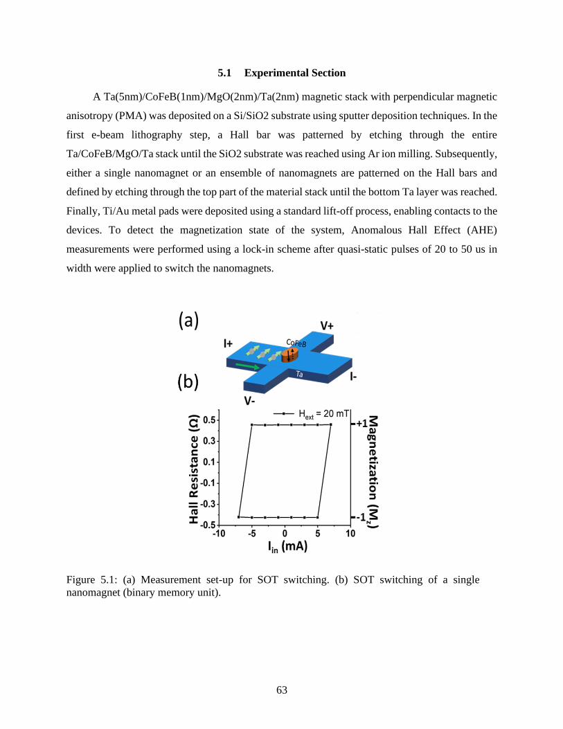
63
5.1 Experimental Section
A Ta(5nm)/CoFeB(1nm)/MgO(2nm)/Ta(2nm) magnetic stack with perpendicular magnetic
anisotropy (PMA) was deposited on a Si/SiO2 substrate using sputter deposition techniques. In the
first e-beam lithography step, a Hall bar was patterned by etching through the entire
Ta/CoFeB/MgO/Ta stack until the SiO2 substrate was reached using Ar ion milling. Subsequently,
either a single nanomagnet or an ensemble of nanomagnets are patterned on the Hall bars and
defined by etching through the top part of the material stack until the bottom Ta layer was reached.
Finally, Ti/Au metal pads were deposited using a standard lift-off process, enabling contacts to the
devices. To detect the magnetization state of the system, Anomalous Hall Effect (AHE)
measurements were performed using a lock-in scheme after quasi-static pulses of 20 to 50 us in
width were applied to switch the nanomagnets.
Figure 5.1: (a) Measurement set-up for SOT switching. (b) SOT switching of a single
nanomagnet (binary memory unit).
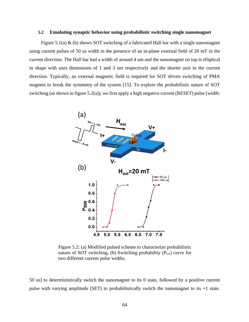
64
5.2 Emulating synaptic behavior using probabilistic switching single nanomagnet
Figure 5.1(a) & (b) shows SOT switching of a fabricated Hall bar with a single nanomagnet
using current pulses of 50 us width in the presence of an in-plane external field of 20 mT in the
current direction. The Hall bar had a width of around 4 um and the nanomagnet on top is elliptical
in shape with axes dimensions of 1 and 3 um respectively and the shorter axis in the current
direction. Typically, an external magnetic field is required for SOT driven switching of PMA
magnets to break the symmetry of the system [15]. To explore the probabilistic nature of SOT
switching (as shown in figure 5.2(a)), we first apply a high negative current (RESET) pulse [width:
50 us] to deterministically switch the nanomagnet to its 0 state, followed by a positive current
pulse with varying amplitude (SET) to probabilistically switch the nanomagnet to its +1 state.
Figure 5.2: (a) Modified pulsed scheme to characterize probabilistic
nature of SOT switching. (b) Switching probability (Psw) curve for
two different current pulse widths.
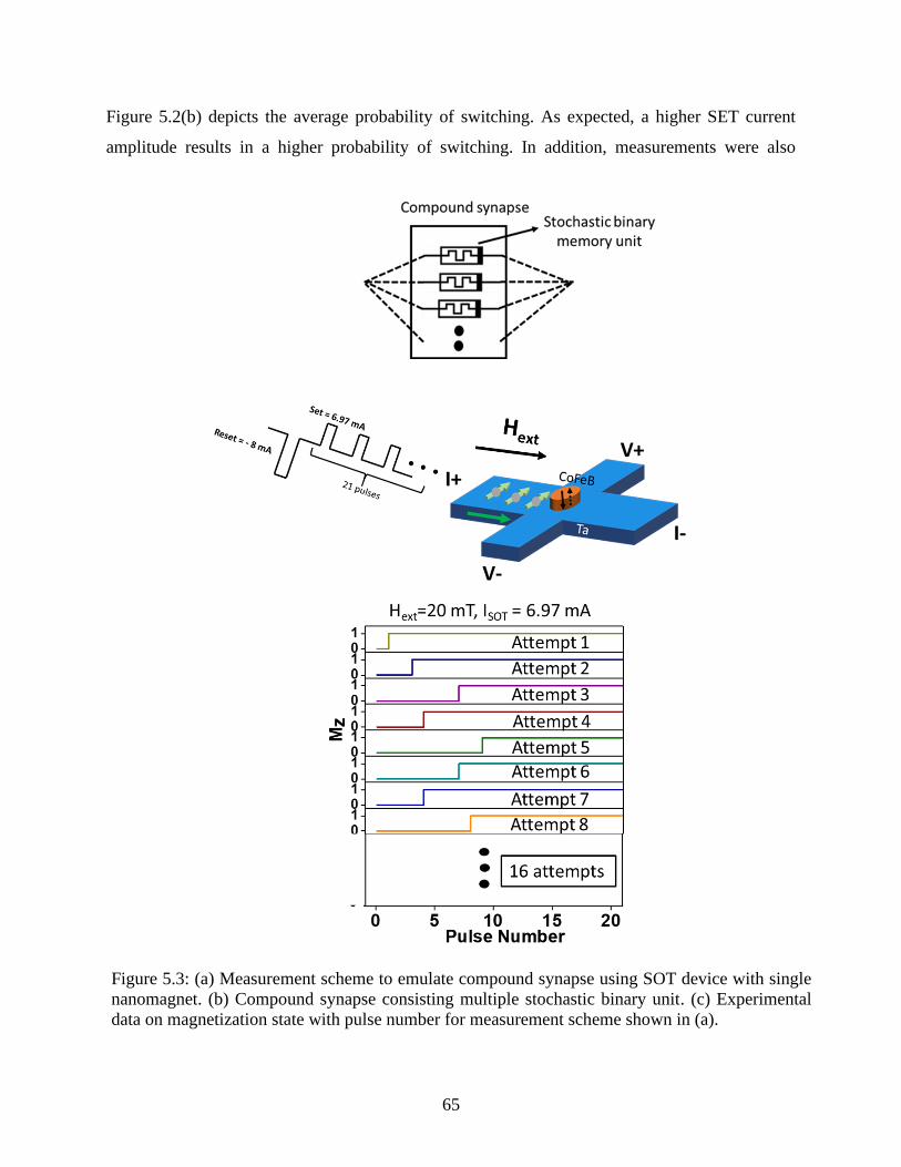
65
Figure 5.2(b) depicts the average probability of switching. As expected, a higher SET current
amplitude results in a higher probability of switching. In addition, measurements were also
Figure 5.3: (a) Measurement scheme to emulate compound synapse using SOT device with single
nanomagnet. (b) Compound synapse consisting multiple stochastic binary unit. (c) Experimental
data on magnetization state with pulse number for measurement scheme shown in (a).
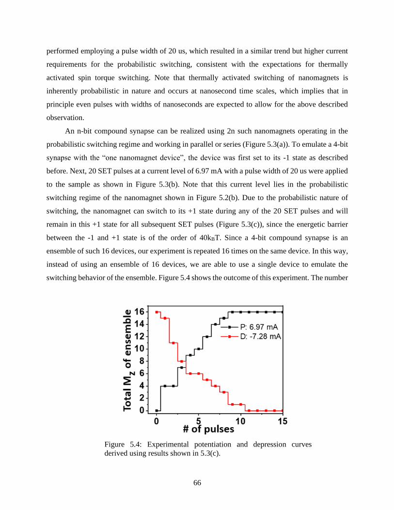
66
performed employing a pulse width of 20 us, which resulted in a similar trend but higher current
requirements for the probabilistic switching, consistent with the expectations for thermally
activated spin torque switching. Note that thermally activated switching of nanomagnets is
inherently probabilistic in nature and occurs at nanosecond time scales, which implies that in
principle even pulses with widths of nanoseconds are expected to allow for the above described
observation.
An n-bit compound synapse can be realized using 2n such nanomagnets operating in the
probabilistic switching regime and working in parallel or series (Figure 5.3(a)). To emulate a 4-bit
synapse with the “one nanomagnet device”, the device was first set to its -1 state as described
before. Next, 20 SET pulses at a current level of 6.97 mA with a pulse width of 20 us were applied
to the sample as shown in Figure 5.3(b). Note that this current level lies in the probabilistic
switching regime of the nanomagnet shown in Figure 5.2(b). Due to the probabilistic nature of
switching, the nanomagnet can switch to its +1 state during any of the 20 SET pulses and will
remain in this +1 state for all subsequent SET pulses (Figure 5.3(c)), since the energetic barrier
between the -1 and +1 state is of the order of 40kBT. Since a 4-bit compound synapse is an
ensemble of such 16 devices, our experiment is repeated 16 times on the same device. In this way,
instead of using an ensemble of 16 devices, we are able to use a single device to emulate the
switching behavior of the ensemble. Figure 5.4 shows the outcome of this experiment. The number
Figure 5.4: Experimental potentiation and depression curves
derived using results shown in 5.3(c).
67
of nanomagnets switched is plotted versus the SET pulse number. The black line clearly illustrates
the increasing probability of finding the one nanomagnet switched in all 16 repeated experiments
in its +1 state. Such behavior is analogous to the potentiation (P) curve of an analog synapse where
the conductance increases gradually with the number of input pulses. Similarly, depression (D)
operation can be emulated with our “one nanomagnet device” when input current pulses of -7.28
mA are used – see red curve in Figure 5.4. Note that by using an MTJ structure instead of our
nanomagnet, the plot in Figure 5.4 would result in an incremental change in conductance through
the MTJ with the number of pulses instead of a change in anomalous Hall resistance, making the
approach much more technology relevant and feasible.
5.3 Mathematical modeling of compound synapse
The P and D behavior of compound synapse can be captured using a simple mathematical
model consisting of 16 independent binary variables, each having a finite probability of switching
for a single pulse (p). During one cycle of potentiation and depression, each one of the 16 variables
can probabilistically switch for each of the input pulse and the number of variables switched are
plotted with respect to the number of input pulses. Grey lines in Figure 5.5(b) corresponds to
individual P and D cycles while the red line in Figure 5.5(b) is average of 100 such cycles. P and
D curves of compound synapse is nonlinear with respect to the pulse number but shows saturating
behavior. Such non-linear behavior is observed even for analog type RRAM memristors due to
characteristics of filaments formation. For neural networks, non-linear behavior has a detrimental
effect on the accuracy of network and to improve the linearity, modified pulse-schemes are being
explored. In such approach, instead of using identical pulses, pulses with either incremental pulse-
width or pulse-amplitude (as shown in Figure 5.5(c)) are used. This approach has extra circuit-
area, time and power cost associated with it compared to identical pulse scheme. We are exploring
such a scheme for the compound synapse approach assuming probability of switching has
sigmoidal dependency on the pulse-amplitude. Figure 5.5(d) shows mathematically expected
potentiation and depression for incremental amplitude pulse scheme, which shows improved
linearity.
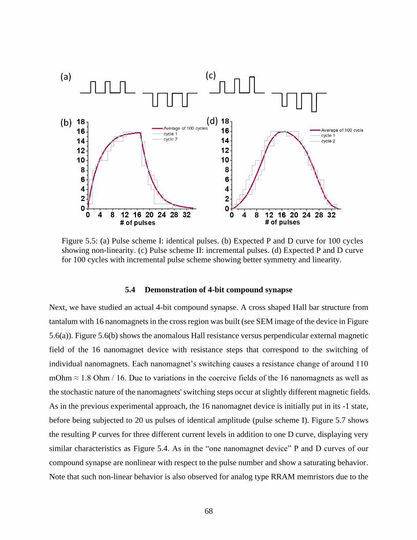
68
5.4 Demonstration of 4-bit compound synapse
Next, we have studied an actual 4-bit compound synapse. A cross shaped Hall bar structure from
tantalum with 16 nanomagnets in the cross region was built (see SEM image of the device in Figure
5.6(a)). Figure 5.6(b) shows the anomalous Hall resistance versus perpendicular external magnetic
field of the 16 nanomagnet device with resistance steps that correspond to the switching of
individual nanomagnets. Each nanomagnet’s switching causes a resistance change of around 110
mOhm ≈ 1.8 Ohm / 16. Due to variations in the coercive fields of the 16 nanomagnets as well as
the stochastic nature of the nanomagnets' switching steps occur at slightly different magnetic fields.
As in the previous experimental approach, the 16 nanomagnet device is initially put in its -1 state,
before being subjected to 20 us pulses of identical amplitude (pulse scheme I). Figure 5.7 shows
the resulting P curves for three different current levels in addition to one D curve, displaying very
similar characteristics as Figure 5.4. As in the “one nanomagnet device” P and D curves of our
compound synapse are nonlinear with respect to the pulse number and show a saturating behavior.
Note that such non-linear behavior is also observed for analog type RRAM memristors due to the
Figure 5.5: (a) Pulse scheme I: identical pulses. (b) Expected P and D curve for 100 cycles
showing non-linearity. (c) Pulse scheme II: incremental pulses. (d) Expected P and D curve
for 100 cycles with incremental pulse scheme showing better symmetry and linearity.
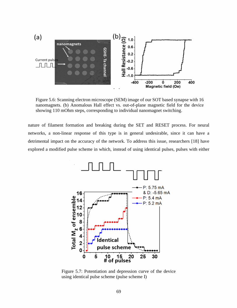
69
nature of filament formation and breaking during the SET and RESET process. For neural
networks, a non-linear response of this type is in general undesirable, since it can have a
detrimental impact on the accuracy of the network. To address this issue, researchers [18] have
explored a modified pulse scheme in which, instead of using identical pulses, pulses with either
Figure 5.6: Scanning electron microscope (SEM) image of our SOT based synapse with 16
nanomagnets. (b) Anomalous Hall effect vs. out-of-plane magnetic field for the device
showing 110 mOhm steps, corresponding to individual nanomagnet switching.
Figure 5.7: Potentiation and depression curve of the device
using identical pulse scheme (pulse scheme I)
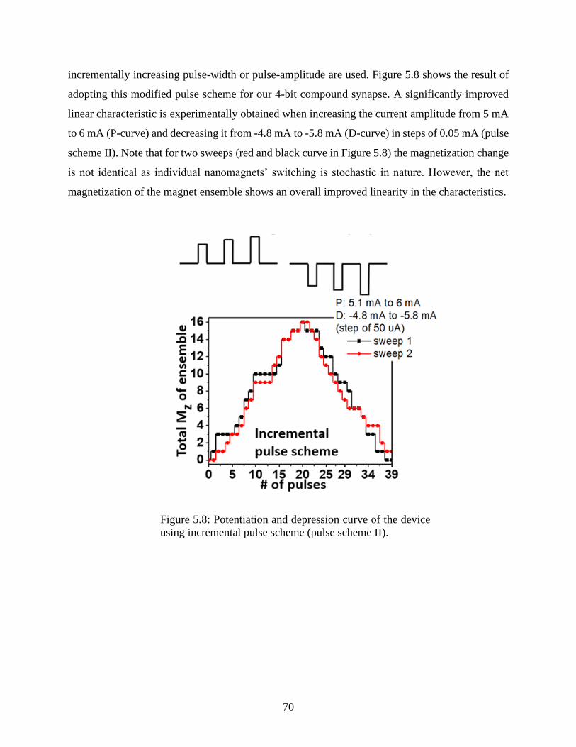
70
incrementally increasing pulse-width or pulse-amplitude are used. Figure 5.8 shows the result of
adopting this modified pulse scheme for our 4-bit compound synapse. A significantly improved
linear characteristic is experimentally obtained when increasing the current amplitude from 5 mA
to 6 mA (P-curve) and decreasing it from -4.8 mA to -5.8 mA (D-curve) in steps of 0.05 mA (pulse
scheme II). Note that for two sweeps (red and black curve in Figure 5.8) the magnetization change
is not identical as individual nanomagnets’ switching is stochastic in nature. However, the net
magnetization of the magnet ensemble shows an overall improved linearity in the characteristics.
Figure 5.8: Potentiation and depression curve of the device
using incremental pulse scheme (pulse scheme II).
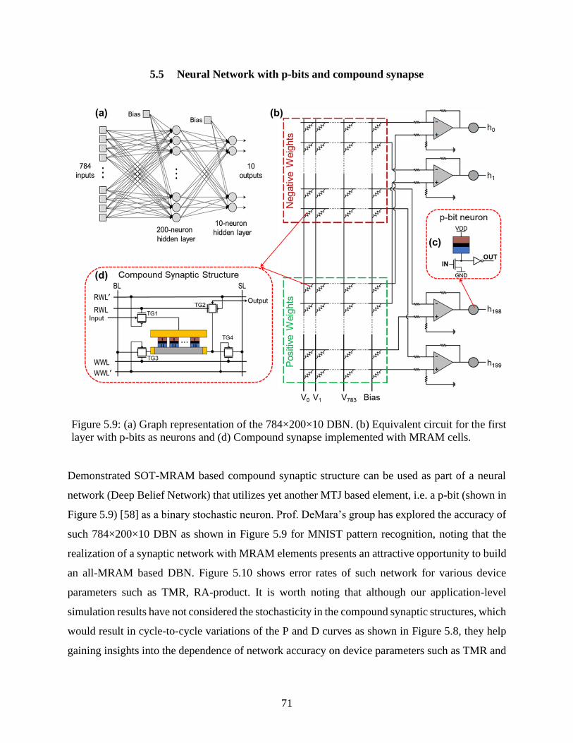
71
5.5 Neural Network with p-bits and compound synapse
Demonstrated SOT-MRAM based compound synaptic structure can be used as part of a neural
network (Deep Belief Network) that utilizes yet another MTJ based element, i.e. a p-bit (shown in
Figure 5.9) [58] as a binary stochastic neuron. Prof. DeMara’s group has explored the accuracy of
such 784×200×10 DBN as shown in Figure 5.9 for MNIST pattern recognition, noting that the
realization of a synaptic network with MRAM elements presents an attractive opportunity to build
an all-MRAM based DBN. Figure 5.10 shows error rates of such network for various device
parameters such as TMR, RA-product. It is worth noting that although our application-level
simulation results have not considered the stochasticity in the compound synaptic structures, which
would result in cycle-to-cycle variations of the P and D curves as shown in Figure 5.8, they help
gaining insights into the dependence of network accuracy on device parameters such as TMR and
Figure 5.9: (a) Graph representation of the 784×200×10 DBN. (b) Equivalent circuit for the first
layer with p-bits as neurons and (d) Compound synapse implemented with MRAM cells.
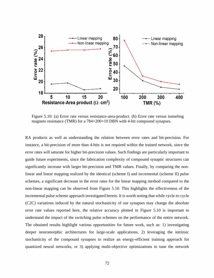
72
RA products as well as understanding the relation between error rates and bit-precision. For
instance, a bit-precision of more than 4-bits is not required within the trained network, since the
error rates will saturate for higher bit-precision values. Such findings are particularly important to
guide future experiments, since the fabrication complexity of compound synaptic structures can
significantly increase with larger bit-precision and TMR values. Finally, by comparing the non-
linear and linear mapping realized by the identical (scheme I) and incremental (scheme II) pulse
schemes, a significant decrease in the error rates for the linear mapping method compared to the
non-linear mapping can be observed from Figure 5.10. This highlights the effectiveness of the
incremental pulse scheme approach investigated herein. It is worth noting that while cycle-to cycle
(C2C) variations induced by the natural stochasticity of our synapses may change the absolute
error rate values reported here, the relative accuracy plotted in Figure 5.10 is important to
understand the impact of the switching pulse schemes on the performance of the entire network.
The obtained results highlight various opportunities for future work, such as: 1) investigating
deeper neuromorphic architectures for large-scale applications, 2) leveraging the intrinsic
stochasticity of the compound synapses to realize an energy-efficient training approach for
quantized neural networks, or 3) applying multi-objective optimizations to tune the network
Figure 5.10: (a) Error rate versus resistance-area-product. (b) Error rate versus tunneling
magneto resistance (TMR) for a 784×200×10 DBN with 4-bit compound synapses.

73
parameters by including device models in the simulation loop. It is also worthwhile noticing that
the compound synaptic structure proposed here can readily be combined with other neuromorphic
computing architectures as discussed in [84][85][86][28].
To verify the energy improvements of our compound synaptic structure over a CMOS-
based weighted connection, we have utilized the energy consumption values reported in [23] and
[24] to estimate the energy consumption for weighted sum operations in a 784×200×10 DBN using
integer and floating-point (FP) multiplication and add (MAC) operations. As listed in Table I, the
4-bit compound synapse based DBN circuit can realize approximately two orders-of-magnitude
energy improvements over their CMOS-based counterparts. It shall be considered that increasing
the bit-precision in a compound synapse from 4-bit to 16-bit or 32-bit can result in higher energy
consumptions. However, the increased energy values will be negligible compared to the significant
energy reductions that are achieved compared to the integer and FP DBNs. On the other hand, it
is shown in [24] that memory accesses normally consume more energy than arithmetic operations,
while our proposed compound synapses also operate as memory cells, thus enabling in-memory
computations which decreases the memory access energy consumptions to near-zero values, as
listed in Table 5.1.
Finally, it shall be noted that here we have only focused on the energy consumption which
can be realized by our compound synapses, while authors have shown in [19] that the p-bit based
neuron can also contribute to several orders of magnitudes energy reduction with respect to
previous energy-efficient CMOS-based activation functions for DBN structures.
Table 5.1: Energy consumption comparison for weighted-sum operation in a
784×200×10 DBN.

74
In conclusion, we have experimentally demonstrated proof-of-concept 4-bit compound
synapses using probabilistic spin-orbit torque switching. A modified incremental pulse scheme is
shown to result in improved linearity of the synaptic behavior. Furthermore, circuit-level
simulations of DBNs consisting of stochastic spin-torque devices, namely p-bits and compound
synapses show that the linearity in the synaptic behavior and high TMR-values are crucial device
parameters to achieve low error rates.
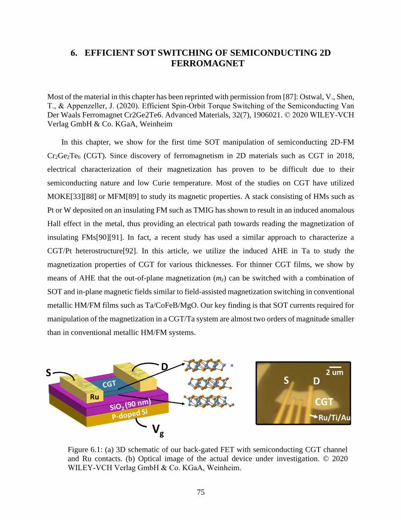
75
EFFICIENT SOT SWITCHING OF SEMICONDUCTING 2D
FERROMAGNET
Most of the material in this chapter has been reprinted with permission from [87]: Ostwal, V., Shen,
T., & Appenzeller, J. (2020). Efficient Spin‐Orbit Torque Switching of the Semiconducting Van
Der Waals Ferromagnet Cr2Ge2Te6. Advanced Materials, 32(7), 1906021. © 2020 WILEY‐VCH
Verlag GmbH & Co. KGaA, Weinheim
In this chapter, we show for the first time SOT manipulation of semiconducting 2D-FM
Cr2Ge2Te6 (CGT). Since discovery of ferromagnetism in 2D materials such as CGT in 2018,
electrical characterization of their magnetization has proven to be difficult due to their
semiconducting nature and low Curie temperature. Most of the studies on CGT have utilized
MOKE[33][88] or MFM[89] to study its magnetic properties. A stack consisting of HMs such as
Pt or W deposited on an insulating FM such as TMIG has shown to result in an induced anomalous
Hall effect in the metal, thus providing an electrical path towards reading the magnetization of
insulating FMs[90][91]. In fact, a recent study has used a similar approach to characterize a
CGT/Pt heterostructure[92]. In this article, we utilize the induced AHE in Ta to study the
magnetization properties of CGT for various thicknesses. For thinner CGT films, we show by
means of AHE that the out-of-plane magnetization (mz) can be switched with a combination of
SOT and in-plane magnetic fields similar to field-assisted magnetization switching in conventional
metallic HM/FM films such as Ta/CoFeB/MgO. Our key finding is that SOT currents required for
manipulation of the magnetization in a CGT/Ta system are almost two orders of magnitude smaller
than in conventional metallic HM/FM systems.
Figure 6.1: (a) 3D schematic of our back-gated FET with semiconducting CGT channel
and Ru contacts. (b) Optical image of the actual device under investigation. © 2020
WILEY‐VCH Verlag GmbH & Co. KGaA, Weinheim.
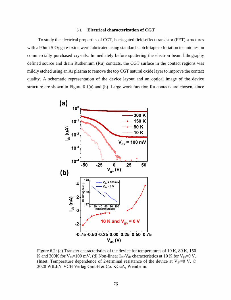
76
6.1 Electrical characterization of CGT
To study the electrical properties of CGT, back-gated field-effect transistor (FET) structures
with a 90nm SiO2 gate-oxide were fabricated using standard scotch-tape exfoliation techniques on
commercially purchased crystals. Immediately before sputtering the electron beam lithography
defined source and drain Ruthenium (Ru) contacts, the CGT surface in the contact regions was
mildly etched using an Ar plasma to remove the top CGT natural oxide layer to improve the contact
quality. A schematic representation of the device layout and an optical image of the device
structure are shown in Figure 6.1(a) and (b). Large work function Ru contacts are chosen, since
Figure 6.2: (c) Transfer characteristics of the device for temperatures of 10 K, 80 K, 150
K and 300K for Vds=100 mV. (d) Non-linear Ids-Vds characteristics at 10 K for Vgs=0 V.
(Inset: Temperature dependence of 2-terminal resistance of the device at Vgs=0 V. ©
2020 WILEY‐VCH Verlag GmbH & Co. KGaA, Weinheim.
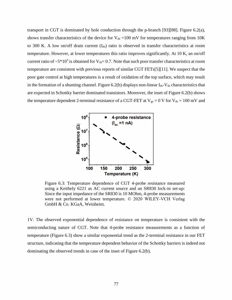
77
transport in CGT is dominated by hole conduction through the p-branch [93][88]. Figure 6.2(a),
shows transfer characteristics of the device for Vds =100 mV for temperatures ranging from 10K
to 300 K. A low on/off drain current (Ids) ratio is observed in transfer characteristics at room
temperature. However, at lower temperatures this ratio improves significantly. At 10 K, an on/off
current ratio of ~5*103 is obtained for Vds= 0.7. Note that such poor transfer characteristics at room
temperature are consistent with previous reports of similar CGT FETs[5][11]. We suspect that the
poor gate control at high temperatures is a result of oxidation of the top surface, which may result
in the formation of a shunting channel. Figure 6.2(b) displays non-linear Ids-Vds characteristics that
are expected in Schottky barrier dominated transistors. Moreover, the inset of Figure 6.2(b) shows
the temperature dependent 2-terminal resistance of a CGT-FET at Vgs = 0 V for Vds = 100 mV and
1V. The observed exponential dependence of resistance on temperature is consistent with the
semiconducting nature of CGT. Note that 4-probe resistance measurements as a function of
temperature (Figure 6.3) show a similar exponential trend as the 2-terminal resistance in our FET
structure, indicating that the temperature dependent behavior of the Schottky barriers is indeed not
dominating the observed trends in case of the inset of Figure 6.2(b).
Figure 6.3: Temperature dependence of CGT 4-probe resistance measured
using a Keithely 6221 as AC current source and an SR830 lock-in set-up:
Since the input impedance of the SR830 is 10 MOhm, 4-probe measurements
were not performed at lower temperature. © 2020 WILEY‐VCH Verlag
GmbH & Co. KGaA, Weinheim.
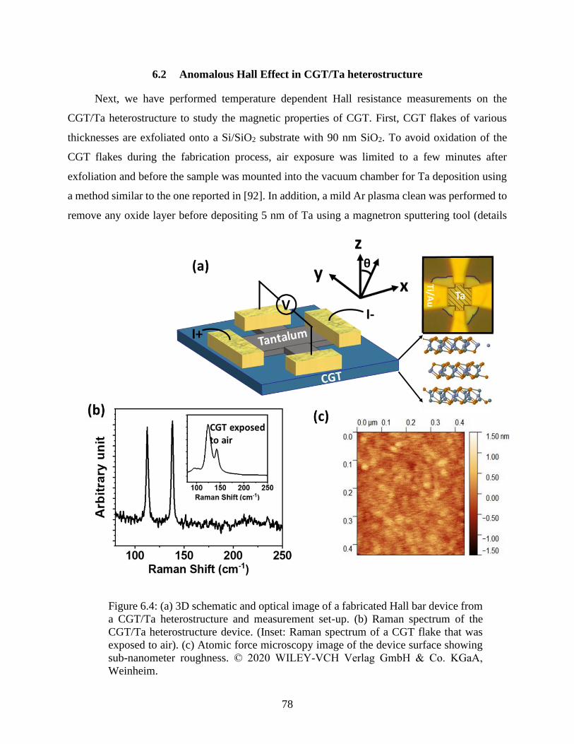
78
6.2 Anomalous Hall Effect in CGT/Ta heterostructure
Next, we have performed temperature dependent Hall resistance measurements on the
CGT/Ta heterostructure to study the magnetic properties of CGT. First, CGT flakes of various
thicknesses are exfoliated onto a Si/SiO2 substrate with 90 nm SiO2. To avoid oxidation of the
CGT flakes during the fabrication process, air exposure was limited to a few minutes after
exfoliation and before the sample was mounted into the vacuum chamber for Ta deposition using
a method similar to the one reported in [92]. In addition, a mild Ar plasma clean was performed to
remove any oxide layer before depositing 5 nm of Ta using a magnetron sputtering tool (details
Figure 6.4: (a) 3D schematic and optical image of a fabricated Hall bar device from
a CGT/Ta heterostructure and measurement set-up. (b) Raman spectrum of the
CGT/Ta heterostructure device. (Inset: Raman spectrum of a CGT flake that was
exposed to air). (c) Atomic force microscopy image of the device surface showing
sub-nanometer roughness. © 2020 WILEY‐VCH Verlag GmbH & Co. KGaA,
Weinheim.
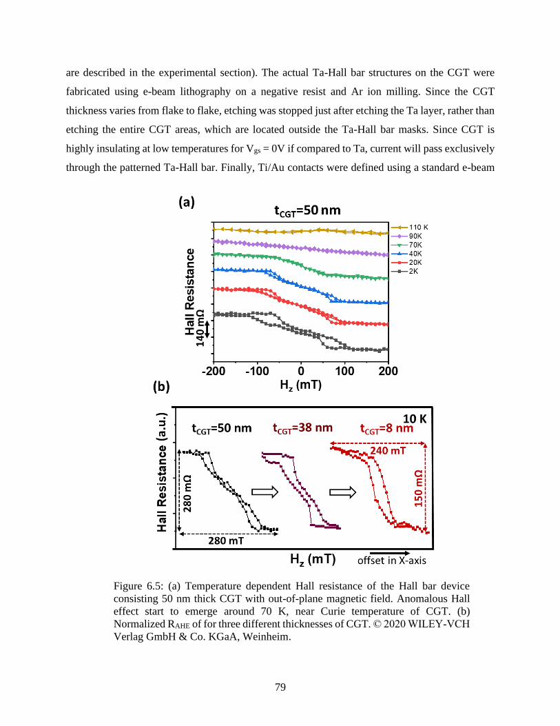
79
are described in the experimental section). The actual Ta-Hall bar structures on the CGT were
fabricated using e-beam lithography on a negative resist and Ar ion milling. Since the CGT
thickness varies from flake to flake, etching was stopped just after etching the Ta layer, rather than
etching the entire CGT areas, which are located outside the Ta-Hall bar masks. Since CGT is
highly insulating at low temperatures for Vgs = 0V if compared to Ta, current will pass exclusively
through the patterned Ta-Hall bar. Finally, Ti/Au contacts were defined using a standard e-beam
Figure 6.5: (a) Temperature dependent Hall resistance of the Hall bar device
consisting 50 nm thick CGT with out-of-plane magnetic field. Anomalous Hall
effect start to emerge around 70 K, near Curie temperature of CGT. (b)
Normalized RAHE of for three different thicknesses of CGT. © 2020 WILEY‐VCH
Verlag GmbH & Co. KGaA, Weinheim.
80
lithography and lift-off process. Figure 6.4(a) shows the measurement set-up and a representative
optical image of a device. Temperature dependent Hall resistance measurements under out-of-
plane (oop) magnetic fields (Hz) were performed using an excitation AC current (Iac) of 10 uA and
a lock-in set-up. Raman spectroscopy data were gathered to confirm the quality of the CGT films.
Unlike the Raman spectra reported previously for CGT FETs, which were exposed to air [93], the
Raman spectra of our CGT/Ta Hall bar devices (with 50 nm CGT) show sharp peaks at
approximately 112 cm-1 and 138 cm-1 (see Figure 6.4(b)), consistent with previously reported
Raman spectra on single crystal CGT [94][95]. The surface roughness of the fabricated devices is
in the sub-nanometer range (Figure 6.4(c)) even after the Ta deposition, further highlighting the
process control achieved. Figure 6.5(a) shows the Hall resistance versus Hz for a Hall bar device
from a 50 nm thick CGT flake. As apparent from fig. 6.5(a), the anomalous Hall resistance (RAHE),
i.e. the out-of-plane magnetization (mz) starts to emerge at around 70 K, near the expected Curie
temperature of CGT[88][96]. Lower temperatures result in a larger hysteresis. However, even at
2K the magnetization remanence remains almost zero. Similar measurements were performed on
devices from thinner CGT films (tCGT). Normalized RAHE curves at 10 K for tCGT = 50 nm, 38 nm
and 8 nm are displayed in Figure 6.5(d). If compared with the CGT (50 nm)/Ta heterostructure
(device #1), the RAHE of a CGT (38 nm)/Ta heterostructure (device #2) and a CGT (8 nm)/Ta
heterostructure (device #3) show progressively larger remanences with a much squarer shaped
hysteresis as expected for a magnet with perpendicular magnetic anisotropy (PMA). Such
thickness dependent magnetization curves have been observed previously using MOKE [88] and
are here obtained using electrical measurements similar to [92].
6.3 SOT switching of CGT
Having demonstrated the PMA behavior of thin CGT flakes at low temperatures, we are in a
position to explore the feasibility of SOT switching by means of currents through the Ta-layer in
contact with the semiconducting magnet. When current is passed through a heavy metal that
exhibits GSHE such as Ta using a configuration as displayed in Figure 6.6(a), spins generated at
the interface are oriented in the y-direction and hence on their own cannot deterministically switch
mz due to symmetry reasons. However, an in-plane magnetic field applied along the current
direction (Hx) can break the symmetry of the system and spin orbit torque can be utilized to
deterministically switch mz in this case. Hence, when the magnetic field is swept in the current
81
direction (Hx) in the presence of a negative or positive DC current a clockwise or counterclockwise
hysteresis loop of mz results respectively [31][97] analogous to a charge current sweep under
positive or negative magnetic fields Hx [16]. On the other hand, the same charge currents are not
expected to result in any hysteresis loop if a magnetic field Hy is applied perpendicular to the
current direction for our PMA magnet with its magnetization in the z-direction. Last, a current
polarity independent hysteresis loop is expected if a magnetic field Hz is swept, a field that is in
the same direction as the magnetization of the PMA magnet.
Exactly these three sets of experiments are displayed in Figure 6.6(b), (c) and (d). The Hall
resistance of device #3 (AFM image is shown in Figure 6.6(a)) was measured at 10K with an Iac=4
uA, using a lock-in set-up in the presence of DC currents (Idc) of different magnitude and
polarization. Magnetic fields are swept in the x-, y-, and z-direction respectively as discussed
above. The observed behavior is largely consistent with the expressed expectations under different
magnetic field and charge current conditions. As shown in Figure 6.6(c), while sweeping Hx, RAHE
(i.e. mz) switching loops are observed even in the absence of Hz and the polarity of the switching
loops is reversed between Idc=+100 uA and –100 uA. Note that the counterclockwise and
clockwise switching under positive and negative charge currents, respectively, is opposite
compared to Ta/CoFeB [16] and W/CoFeB [98] systems due to an inversion of the stacking
sequence of HM and FM layers. Our observations are also consistent with the observed SOT
switching in a Tm3Fe5O12/Tungsten (TMIG/W) heterostructure as reported before [9], since W in
their experiments and Ta in our experiments exhibit a spin Hall angle with the same polarity. On
the other hand, no such RAHE loops are observed while sweeping Hy (Figure 6.6(d)).
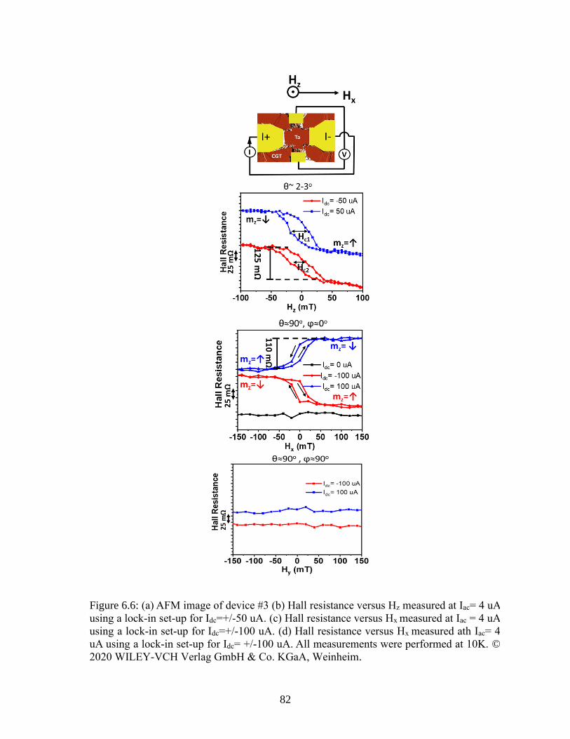
82
Figure 6.6: (a) AFM image of device #3 (b) Hall resistance versus Hz measured at Iac= 4 uA
using a lock-in set-up for Idc=+/-50 uA. (c) Hall resistance versus Hx measured at Iac = 4 uA
using a lock-in set-up for Idc=+/-100 uA. (d) Hall resistance versus Hx measured ath Iac= 4
uA using a lock-in set-up for Idc= +/-100 uA. All measurements were performed at 10K. ©
2020 WILEY‐VCH Verlag GmbH & Co. KGaA, Weinheim.
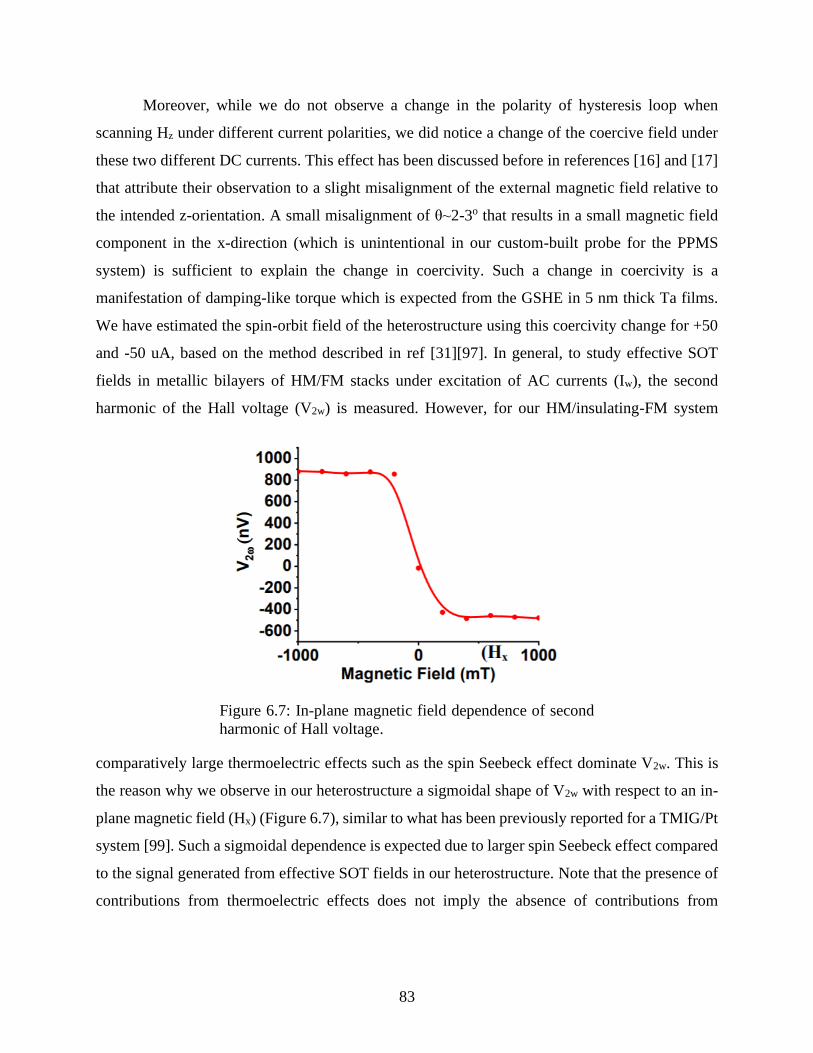
83
Moreover, while we do not observe a change in the polarity of hysteresis loop when
scanning Hz under different current polarities, we did notice a change of the coercive field under
these two different DC currents. This effect has been discussed before in references [16] and [17]
that attribute their observation to a slight misalignment of the external magnetic field relative to
the intended z-orientation. A small misalignment of θ~2-3o that results in a small magnetic field
component in the x-direction (which is unintentional in our custom-built probe for the PPMS
system) is sufficient to explain the change in coercivity. Such a change in coercivity is a
manifestation of damping-like torque which is expected from the GSHE in 5 nm thick Ta films.
We have estimated the spin-orbit field of the heterostructure using this coercivity change for +50
and -50 uA, based on the method described in ref [31][97]. In general, to study effective SOT
fields in metallic bilayers of HM/FM stacks under excitation of AC currents (Iw), the second
harmonic of the Hall voltage (V2w) is measured. However, for our HM/insulating-FM system
comparatively large thermoelectric effects such as the spin Seebeck effect dominate V2w. This is
the reason why we observe in our heterostructure a sigmoidal shape of V2w with respect to an in-
plane magnetic field (Hx) (Figure 6.7), similar to what has been previously reported for a TMIG/Pt
system [99]. Such a sigmoidal dependence is expected due to larger spin Seebeck effect compared
to the signal generated from effective SOT fields in our heterostructure. Note that the presence of
contributions from thermoelectric effects does not imply the absence of contributions from
Figure 6.7: In-plane magnetic field dependence of second
harmonic of Hall voltage.
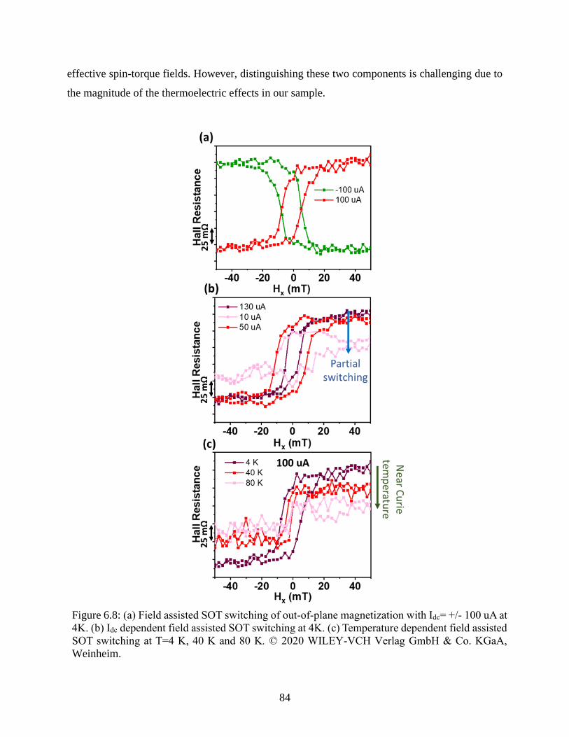
84
effective spin-torque fields. However, distinguishing these two components is challenging due to
the magnitude of the thermoelectric effects in our sample.
Figure 6.8: (a) Field assisted SOT switching of out-of-plane magnetization with Idc= +/- 100 uA at
4K. (b) Idc dependent field assisted SOT switching at 4K. (c) Temperature dependent field assisted
SOT switching at T=4 K, 40 K and 80 K. © 2020 WILEY‐VCH Verlag GmbH & Co. KGaA,
Weinheim.
85
Hence, we have focused our experiments on the direct observation of SOT switching rather
than analyzing effective SOT fields. The sum of these experimental findings unambiguously
proves the successful SOT switching in a Ta/CGT heterostructure that is reported here for the first
time. Next, we are interested in exploring how efficient the charge-to-spin conversion in our
Ta/CGT stacks is in comparison to the reported SOT switching in other heterostructures. Figure
6.8 shows device characteristics of yet another Ta/CGT device. As in the case discussed in the
context of Figure 6.5(c), clear SOT switching with the expected reversal of the hysteresis loop is
observed in Figure 6.8(a) when sweeping Hx under positive and negative charge current polarities
at 4K. Moreover, as expected from previous studies [91], higher charge currents require smaller
Hx and vice versa to change the magnetization of our CGT magnet with PMA (see Figure 6.7(b)).
Note that too small Idc-values result in incomplete (partial) reversal of the magnetization direction
since in a large FM with a size of a few µm2, such as in our experiment, SOT switching is driven
by domain nucleation [64][65][102]. To further evaluate the SOT switching, we have also
characterized device#4 for temperatures of 40K and 80 K. Since the magnetization switching of
our micro-scale device is a thermally assisted process (along with a lowered magnetic anisotropy
at higher temperatures), we expect easier magnetization switching, i.e. lower in-plane fields
required for switching at higher temperatures. This behavior is observed in Figure 6.8(c) for a
constant current of 100 uA. At 80 K, a negligible RAHE loop is observed due to the loss of
ferromagnetism near the Curie temperature of CGT.
Plotting the actual Idc and critical Hx-fields for complete switching allows creating a switching
phase diagram – Figure 6.9(a) that shows the typical diamond shape [98]. Current and magnetic
field value pairs outside the diamond guarantee SOT switching. In the presence of an in-plane field
of approximately 20 mT an Idc-value of 50 uA, which corresponds to a current density of around
5*105 A/cm2 is sufficient to switch mz. Fig. 6.9(b) puts our experimental findings on SOT
switching into the context of previously reported data on other hetero stacks. It is apparent that
metallic heavy metal/ ferromagnet (HM/FM) heterostructures such as Ta/CoFeB [16] or Pt/FGT
[103][104] require in general high critical current densities of around 107 A/cm2 for field-assisted
SOT switching as a result of current shunting through the magnet and large Ms-values of the
magnets used. On the other hand, integration of insulating FMs such as TMIG [90] or usage of TI
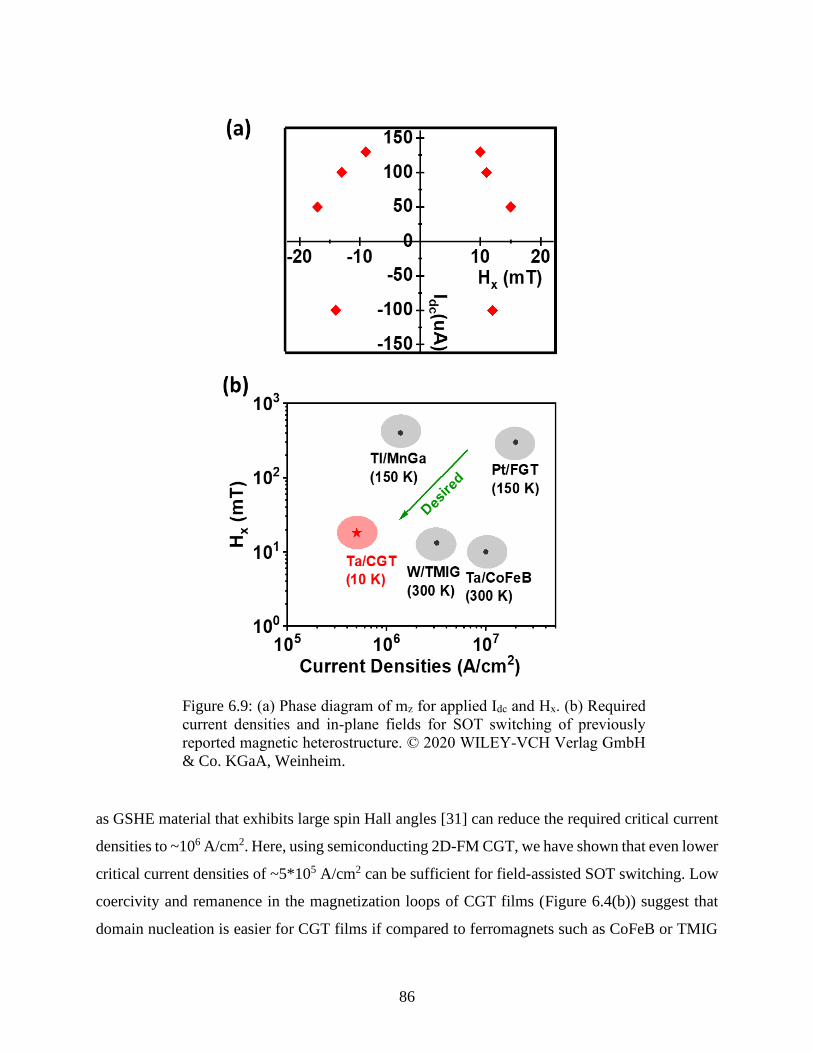
86
as GSHE material that exhibits large spin Hall angles [31] can reduce the required critical current
densities to ~106 A/cm2. Here, using semiconducting 2D-FM CGT, we have shown that even lower
critical current densities of ~5*105 A/cm2 can be sufficient for field-assisted SOT switching. Low
coercivity and remanence in the magnetization loops of CGT films (Figure 6.4(b)) suggest that
domain nucleation is easier for CGT films if compared to ferromagnets such as CoFeB or TMIG
Figure 6.9: (a) Phase diagram of mz for applied Idc and Hx. (b) Required
current densities and in-plane fields for SOT switching of previously
reported magnetic heterostructure. © 2020 WILEY‐VCH Verlag GmbH
& Co. KGaA, Weinheim.

87
which show sharp switching at coercivity. We believe that this could be one of the possible reasons
for the low current densities required for SOT switching in our experiments. However, out-of-
plane fields required for magnetization saturation are not small (around 50 mT as shown in fig.
6.5(b)) which suggest even though nucleation is easier, SOT switching of total magnetization
would require substantial effective fields and further investigation is required to understand SOT
switching mechanism in these micron-scale devices.
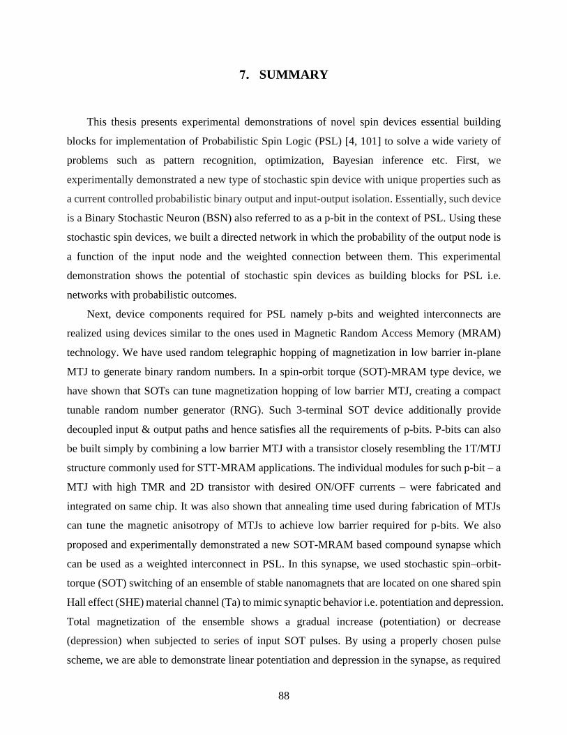
88
SUMMARY
This thesis presents experimental demonstrations of novel spin devices essential building
blocks for implementation of Probabilistic Spin Logic (PSL) [4, 101] to solve a wide variety of
problems such as pattern recognition, optimization, Bayesian inference etc. First, we
experimentally demonstrated a new type of stochastic spin device with unique properties such as
a current controlled probabilistic binary output and input-output isolation. Essentially, such device
is a Binary Stochastic Neuron (BSN) also referred to as a p-bit in the context of PSL. Using these
stochastic spin devices, we built a directed network in which the probability of the output node is
a function of the input node and the weighted connection between them. This experimental
demonstration shows the potential of stochastic spin devices as building blocks for PSL i.e.
networks with probabilistic outcomes.
Next, device components required for PSL namely p-bits and weighted interconnects are
realized using devices similar to the ones used in Magnetic Random Access Memory (MRAM)
technology. We have used random telegraphic hopping of magnetization in low barrier in-plane
MTJ to generate binary random numbers. In a spin-orbit torque (SOT)-MRAM type device, we
have shown that SOTs can tune magnetization hopping of low barrier MTJ, creating a compact
tunable random number generator (RNG). Such 3-terminal SOT device additionally provide
decoupled input & output paths and hence satisfies all the requirements of p-bits. P-bits can also
be built simply by combining a low barrier MTJ with a transistor closely resembling the 1T/MTJ
structure commonly used for STT-MRAM applications. The individual modules for such p-bit – a
MTJ with high TMR and 2D transistor with desired ON/OFF currents – were fabricated and
integrated on same chip. It was also shown that annealing time used during fabrication of MTJs
can tune the magnetic anisotropy of MTJs to achieve low barrier required for p-bits. We also
proposed and experimentally demonstrated a new SOT-MRAM based compound synapse which
can be used as a weighted interconnect in PSL. In this synapse, we used stochastic spin–orbit-
torque (SOT) switching of an ensemble of stable nanomagnets that are located on one shared spin
Hall effect (SHE) material channel (Ta) to mimic synaptic behavior i.e. potentiation and depression.
Total magnetization of the ensemble shows a gradual increase (potentiation) or decrease
(depression) when subjected to series of input SOT pulses. By using a properly chosen pulse
scheme, we are able to demonstrate linear potentiation and depression in the synapse, as required
89
for many neuromorphic architectures. Circuit simulations of deep belief network (DBN) consisting
of p-bits based neurons and compound synapses show capabilities of performing pattern
recognition tasks on MINIST datasets.
Finally, we have explored novel 2-Dimensional Ferromagnets (2D-FMs) for their applications
in future spintronics devices. In conclusion, by integrating semiconducting 2D-FMs and HMs with
high SOC, we have demonstrated strong spin-orbit torque effects in CGT/Ta heterostructures. We
have experimentally demonstrated that out-of-plane magnetization of CGT can be manipulated by
flowing a charge current through Tantalum, in the presence of an in-plane magnetic field. Current
densities as low as 5*105 A/cm2 are sufficient for SOT switching in the presence of in-plane fields
of 20 mT. Spin-torque switching as demonstrated here along with the previously explored gate
voltage manipulation of 2D semiconducting FMs may enable novel van der Waals heterostructures
for the realization of novel low power spintronic devices for memory and logic applications.
90
REFERENCES
[1] S. E. Thompson and S. Parthasarathy, “Moore’s law: the future of Si microelectronics,”
Mater. Today, vol. 9, no. 6, pp. 20–25, 2006.
[2] Samuel K. Moore, “Another Step Toward the End of Moore’s Law,” IEEE Spectrum, pp.
9–10, 2019.
[3] M. Waldrop, “More than moore,” Nature, vol. 530, p. 145, 2016.
[4] D. Reinsel, J. Gantz, and J. Rydning, “The Digitization of the World - From Edge to Core,”
Fram. Int. Data Corp., vol. 2018, no. November, p. US44413318, 2018.
[5] D. Reinsel, J. Gantz, and J. Rydning, “The Digitization of the World from Edge to Core,”
Int. Data Corp. Rep., no. November, 2018.
[6] M. I. Jordan and T. M. Mitchell, “Machine learning: Trends, perspectives, and prospects,”
vol. 349, no. 6245, 2015.
[7] J. Von Neumann, The computer and the brain. Yale University Press, 2012.
[8] EDITORIAL, “Big data needs a hardware revolution,” Nature, vol. 541, pp. 133–134, 2015.
[9] S. Khoram, Y. Zha, J. Zhang, and J. Li, “Challenges and opportunities: From near-memory
computing to in-memory computing,” Proc. Int. Symp. Phys. Des., vol. Part F1271, pp. 43–
46, 2017.
[10] and J. C. M. N. Baibich, J. M. Broto, A. Fert, F. Nguyen Van Dau, F. Petroff, P. Etienne,
G. Creuzet, A. Friederich, “Giant Magnetoresistance of (001)Fe/(001)Cr Magnetic
Superlattices,” Phys. Rev. Lett., vol. 61, no. 001, pp. 2472–2475, 1988.
[11] S. Datta and B. Das, “Electronic analog of the electro-optic modulator,” Appl. Phys. Lett.,
vol. 56, no. 7, pp. 665–667, 1990.
[12] M. Bowen et al., “Large magnetoresistance in Fe/MgO/FeCo(001 ) epitaxial tunnel
junctions on GaAs(001),” Appl. Phys. Lett., vol. 79, no. 11, pp. 1655–1657, 2001.
[13] M. Gajek et al., “Spin torque switching of 20 nm magnetic tunnel junctions with
perpendicular anisotropy,” Appl. Phys. Lett., vol. 100, no. 13, pp. 1–4, 2012.
[14] S. Ikeda et al., “A perpendicular-anisotropy CoFeB-MgO magnetic tunnel junction,” Nat.
Mater., vol. 9, no. 9, pp. 721–724, 2010.
[15] S. Bhatti, R. Sbiaa, A. Hirohata, H. Ohno, S. Fukami, and S. N. Piramanayagam,
“Spintronics based random access memory: a review,” Mater. Today, vol. 20, no. 9, pp.
530–548, 2017.
91
[16] L. Liu et al., “Spin-Torque Switching with the Giant Spin Hall Effect of Tantalum,” Science
(80-. )., vol. 336, pp. 555–558, 2012.
[17] A. Sengupta and K. Roy, “Encoding neural and synaptic functionalities in electron spin: A
pathway to efficient neuromorphic computing,” Appl. Phys. Rev., vol. 4, no. 4, 2017.
[18] K. Y. Camsari et al., “From Charge to Spin and Spin to Charge: Stochastic Magnets for
Probabilistic Switching,” Proc. IEEE, vol. 108, no. 8, pp. 1322–1337, 2020.
[19] R. Zand, K. Y. Camsari, S. Datta, and R. F. Demara, “Composable Probabilistic Inference
Networks Using MRAM-based Stochastic Neurons,” arXiv, vol. 15, no. 2, 2018.
[20] B. Sutton, K. Y. Camsari, B. Behin-aein, and S. Datta, “Intrinsic optimization using
stochastic nanomagnets,” Sci. Rep., vol. 7, 2017.
[21] R. Faria, K. Y. Camsari, and S. Datta, “Implementing Bayesian networks with embedded
stochastic MRAM,” AIP Adv., vol. 8, no. March 2018, p. 045101, 2018.
[22] K. Y. Camsari, R. Faria, B. M. Sutton, and S. Datta, “Stochastic p-bits for invertible logic,”
Phys. Rev. X, vol. 7, no. 3, pp. 1–19, 2017.
[23] K. Y. Camsari, S. Salahuddin, and S. Datta, “Implementing p-bits with Embedded MTJ,”
IEEE Electron Device Lett., vol. 38, no. 12, pp. 1767–1770, 2017.
[24] O. Hassan, R. Faria, K. Y. Camsari, J. Z. Sun, and S. Datta, “Low barrier magnet design for
efficient hardware binary stochastic neurons,” IEEE Magn. Lett., vol. 10, p. 4502805, 2019.
[25] J. Kaiser, A. Rustagi, K. Y. Camsari, J. Z. Sun, S. Datta, and P. Upadhyaya,
“Subnanosecond Fluctuations in Low-Barrier Nanomagnets,” arXiv, vol. 10, no. 1, p. 1,
2019.
[26] M. Cubukcu et al., “SOT-MRAM 300mm integration for low power and ultrafast embedded
memories K.,” IEEE Trans. Magn., vol. 54, no. 4, pp. 81–82, 2018.
[27] D. Zhang et al., “Energy-efficient neuromorphic computation based on compound spin
synapse with stochastic learning,” Proc. - IEEE Int. Symp. Circuits Syst., vol. 2015–July,
pp. 1538–1541, 2015.
[28] A. Mondal and A. Srivastava, “In-situ Stochastic Training of MTJ Crossbar based Neural
Networks,” Proc. Int. Symp. Low Power Electron. Des., p. 51, 2018.
[29] & A. J. Ostwal, Vaibhav, Zand Ramtin, DeMara Ron, “A Novel Compound Synapse Using
Probabilistic Spin–Orbit-Torque Switching for MTJ-Based Deep Neural Networks,” IEEE
J. Explor. Solid-State Comput. Devices Circuits Receiv., vol. 5.2, no. September 2019, pp.
182–187, 2020.
92
[30] A. Hirohata, W. Frost, M. Samiepour, and J. Y. Kim, “Perpendicular magnetic anisotropy
in Heusler alloy films and their magnetoresistive junctions,” Materials (Basel)., vol. 11, no.
1, pp. 1–18, 2018.
[31] H. D. K. Nguyen, U. Yugo, and N. H. Pham, “A conductive topological insulator with large
spin Hall effect for ultralow power spin–orbit torque switching,” Nat. Mater., vol. 17, pp.
808–813, 2018.
[32] C. Song, B. Cui, F. Li, X. Zhou, and F. Pan, “Recent progress in voltage control of
magnetism: Materials, mechanisms, and performance,” Prog. Mater. Sci., vol. 87, pp. 33–
82, 2017.
[33] C. Gong et al., “Discovery of intrinsic ferromagnetism in two-dimensional van der Waals
crystals,” Nature, vol. 546, pp. 265–269, 2017.
[34] E. Barré et al., “Spatial Separation of Carrier Spin by the Valley Hall Effect in Monolayer
WSe2 Transistors,” Nano Lett., 2019.
[35] W. Yan et al., “Long Spin Diffusion Length in Few-Layer Graphene Flakes,” Phys. Rev.
Lett., vol. 117, no. 14, pp. 1–6, 2016.
[36] RadisavljevicB et al., “Single-layer MoS2 transistors,” Nat. Nanotechnol., vol. 6, no. 3, pp.
147–150, 2011.
[37] S. B. Desai et al., “MoS2 transistors with 1-nanometer gate lengths,” Science (80-. )., vol.
354, no. 6308, pp. 99–102, 2016.
[38] F. Zhang et al., “Electric-field induced structural transition in vertical MoTe 2 - and Mo 1–
x W x Te 2 -based resistive memories,” Nat. Mater., vol. 18, no. 1, pp. 55–61, 2019.
[39] T. Song et al., “Giant tunneling magnetoresistance in spin-filter van der Waals
heterostructures,” Science (80-. )., vol. 360, no. 6394, pp. 1214–1218, 2018.
[40] F. Liu et al., “Room-temperature ferroelectricity in CuInP 2 S 6 ultrathin flakes,” Nat.
Commun., vol. 7, pp. 1–6, 2016.
[41] M. Bonilla et al., “Strong roomerature ferromagnetism in VSe2 monolayers on van der
Waals substrates,” Nat. Nanotechnol., vol. 13, no. 4, pp. 289–293, 2018.
[42] C. Gong et al., “Discovery of intrinsic ferromagnetism in two-dimensional van der Waals
crystals,” Nature, vol. 546, no. 7657, pp. 265–269, 2017.
[43] B. Huang et al., “Layer-dependent ferromagnetism in a van der Waals crystal down to the
monolayer limit,” Nature, vol. 546, no. 7657, pp. 270–273, 2017.
[44] Z. Fei et al., “Two-dimensional itinerant ferromagnetism in atomically thin Fe3GeTe2,”
Nat. Mater., vol. 17, no. 9, pp. 778–782, 2018.
93
[45] Z. Zhang, J. Shang, C. Jiang, A. Rasmita, W. Gao, and T. Yu, “Direct Photoluminescence
Probing of Ferromagnetism in Monolayer Two-Dimensional CrBr 3,” Nano Lett., vol. 19,
no. 5, pp. 3138–3142, 2019.
[46] S. Wu et al., “The direct observation of ferromagnetic domain of single crystal CrSiTe3,”
AIP Adv., vol. 8, no. 5, pp. 1–6, 2018.
[47] Y. P. F. & G. E. Ivan A. Verzhbitskiy, Hidekazu Kurebayashi, Haixia Cheng, Jun Zhou,
Safe Khan, “Controlling the magnetic anisotropy in Cr2Ge2Te6 by electrostatic gating,”
Nat. Electron., vol. 3, pp. 460–465, 2020.
[48] Z. Wang, D. Sapkota, T. Taniguchi, K. Watanabe, D. Mandrus, and A. F. Morpurgo,
“Tunneling Spin Valves Based on Fe3GeTe2/hBN/Fe3GeTe2 van der Waals
Heterostructures,” Nano Lett., vol. 18, no. 7, pp. 4303–4308, 2018.
[49] S. Jiang, L. Li, Z. Wang, J. Shan, and K. F. Mak, “Spin tunnel field-effect transistors based
on two-dimensional van der Waals heterostructures,” Nat. Electron., vol. 2, no. 4, pp. 159–
163, 2019.
[50] X. Li, J. T. Lü, J. Zhang, L. You, Y. Su, and E. Y. Tsymbal, “Spin-Dependent Transport in
van der Waals Magnetic Tunnel Junctions with Fe3GeTe2 Electrodes,” Nano Lett., vol. 19,
no. 8, pp. 5133–5139, 2019.
[51] V. Ostwal, P. Debashis, R. Faria, Z. Chen, and J. Appenzeller, “Spin-torque devices with
hard axis initialization as Stochastic Binary Neurons,” Sci. Rep., vol. 8, no. 1, pp. 1–8, 2018.
[52] V. Quang Diep, B. Sutton, B. Behin-Aein, and S. Datta, “Spin switches for compact
implementation of neuron and synapse,” Appl. Phys. Lett., vol. 104, no. 22, 2014.
[53] Y. Shim, S. Chen, A. Sengupta, and K. Roy, “Stochastic Spin-Orbit Torque Devices as
Elements for Bayesian Inference,” Sci. Rep., vol. 7, no. 1, pp. 1–9, 2017.
[54] R. Faria, K. Y. Camsari, and S. Datta, “Implementing Bayesian networks with embedded
stochastic MRAM,” AIP Adv., vol. 8, no. 4, 2018.
[55] B. Behin-Aein, V. Diep, and S. Datta, “A building block for hardware belief networks,” Sci.
Rep., vol. 6, no. July, pp. 1–10, 2016.
[56] Y. Shim, A. Jaiswal, and K. Roy, “Ising computation based combinatorial optimization
using spin-Hall effect (SHE) induced stochastic magnetization reversal,” J. Appl. Phys., vol.
121, no. 19, 2017.
[57] P. Debashis, R. Faria, K. Y. Camsari, J. Appenzeller, S. Datta, and Z. Chen, “Experimental
demonstration of nanomagnet networks as hardware for Ising computing,” Tech. Dig. - Int.
Electron Devices Meet. IEDM, p. 34.3.1-34.3.4, 2017.
[58] K. Y. Camsari, R. Faria, B. M. Sutton, and S. Datta, “Stochastic p-bits for invertible logic,”
Phys. Rev. X, vol. 7, 2017.
94
[59] D. Vodenicarevic et al., “Low-Energy Truly Random Number Generation with
Superparamagnetic Tunnel Junctions for Unconventional Computing,” Phys. Rev. Appl.,
vol. 8, no. 5, pp. 1–9, 2017.
[60] A. Mizrahi et al., “Neural-like computing with populations of superparamagnetic basis
functions,” Nat. Commun., vol. 9, no. 1, pp. 1–11, 2018.
[61] M. Bapna and S. A. Majetich, “Current control of time-averaged magnetization in
superparamagnetic tunnel junctions,” Appl. Phys. Lett., vol. 111, no. 24, 2017.
[62] M. Sharad, C. Augustine, G. Panagopoulos, and K. Roy, “Spin-Based Neuron Model with
Domain Wall Magnets as Synapse,” IEEE Trans. Nanotechnol., vol. 11, no. c, pp. 843–853,
2012.
[63] L. Liu, C. Pai, Y. Li, H. W. Tseng, D. C. Ralph, and R. A. Buhrman, “Spin-Torque
Switching with the Giant Spin Hall Effect of Tantalum,” Science (80-. )., vol. 336, pp. 555–
559, 2012.
[64] I. M. Miron et al., “Perpendicular switching of a single ferromagnetic layer induced by in-
plane current injection.,” Nature, vol. 476, pp. 189–193, 2011.
[65] Y. Kim, X. Fong, and K. Roy, “Spin-Orbit-Torque-Based Spin-Dice : A True Random-
Number Generator,” IEEE Magn. Lett., vol. 6, pp. 1–4, 2015.
[66] D. Bhowmik, L. You, and S. Salahuddin, “Spin hall effect clocking of nanomagnetic logic
without a magnetic field,” Nat. Nanotechnol., vol. 9, pp. 59–63, 2014.
[67] V. Ostwal, A. Penumatcha, Y. M. Hung, A. D. Kent, and J. Appenzeller, “Spin-orbit torque
based magnetization switching in Pt/Cu/[Co/Ni]5multilayer structures,” J. Appl. Phys., vol.
122, no. 21, 2017.
[68] L. E. Bassham et al., “A statistical test suite for random and pseudorandom number
generators for cryptographic applications,” Spec. Publ. (NIST SP) - 800-22 Rev 1a, 2010.
[69] A. Fukushima et al., “Spin dice: A scalable truly random number generator based on
spintronics,” Appl. Phys. Express, vol. 7, no. 8, 2014.
[70] W. Scott, D. E. Nikonov, J. Jeffrey, I. A. Young, and B. Heard, “Hybrid Piezoelectric-
Magnetic Neurons : A Proposal for Energy- Efficient Machine Learning,” Proc. ACMSE
2018 Conf. ACM., pp. 3–7, 2018.
[71] A. Sengupta, S. H. Choday, Y. Kim, and K. Roy, “Spin orbit torque based electronic neuron,”
Appl. Phys. Lett., vol. 106, no. 14, p. 143701, 2015.
[72] K. Kim, J. Kim, J. Yu, J. Seo, J. Lee, and K. Choi, “Dynamic energy-accuracy trade-off
using stochastic computing in deep neural networks,” Proc. 53rd Annu. Des. Autom. Conf.
- DAC ’16, no. 1, pp. 1–6, 2016.
95
[73] V. Ostwal and J. Appenzeller, “Spin-Orbit Torque-Controlled Magnetic Tunnel Junction
with Low Thermal Stability for Tunable Random Number Generation,” IEEE Magn. Lett.,
vol. 10, 2019.
[74] Y. M. Lee, J. Hayakawa, S. Ikeda, F. Matsukura, and H. Ohno, “Giant tunnel
magnetoresistance and high annealing stability in CoFeB/MgO/CoFeB magnetic tunnel
junctions with synthetic pinned layer,” Appl. Phys. Lett., vol. 89, 2006.
[75] A. V Penumatcha et al., “Spin-torque switching of a nano-magnet using giant spin hall
effect Spin-torque switching of a nano-magnet using giant spin hall effect,” AIP Adv., vol.
5, 2015.
[76] J. Z. Sun, “Spin-current interaction with a monodomain magnetic body: A model study,”
Phys. Rev. B, vol. 62, pp. 570–578, 2000.
[77] M. Bapna and S. A. Majetich, “Current control of time-averaged magnetization in
superparamagnetic tunnel junctions,” Appl. Phys. Lett., vol. 111, 2018.
[78] M. Cecot et al., “Influence of intermixing at the Ta/CoFeB interface on spin Hall angle in
Ta/CoFeB/MgO heterostructures,” Sci. Rep., vol. 7, 2017.
[79] S. V. Aradhya, G. E. Rowlands, J. Oh, D. C. Ralph, and R. A. Buhrman, “Nanosecond-
Timescale Low Energy Switching of In-Plane Magnetic Tunnel Junctions through Dynamic
Oersted-Field-Assisted Spin Hall Effect,” Nano Lett., vol. 16, pp. 5987–5992, 2016.
[80] C. Shannon, “A mathematical theory of communication,” Bell Syst. Tech. J., vol. XXVII,
1948.
[81] W. F. Brown, “Thermal fluctuations of a single-domain particle,” Phys. Rev., vol. 34, 1963.
[82] J. Bill and R. Legenstein, “A compound memristive synapse model for statistical learning
through STDP in spiking neural networks,” Front. Neurosci., vol. 8, no. DEC, pp. 1–18,
2014.
[83] E. Vianello et al., “HfO2-Based OxRAM Devices as Synapses for Convolutional Neural
Networks,” IEEE Trans. Electron Devices, vol. 62, no. 8, pp. 2494–2501, 2015.
[84] D. Zhang et al., “All Spin Artificial Neural Networks Based on Compound Spintronic
Synapse and Neuron,” IEEE Trans. Biomed. Circuits Syst., vol. 10, no. 4, pp. 828–836,
2016.
[85] C. Gamrat et al., “Spin-Transfer Torque Magnetic Memory as a Stochastic Memristive
Synapse for Neuromorphic Systems,” IEEE Trans. Biomed. Circuits Syst., vol. 9, no. 2, pp.
166–174, 2015.
[86] D. Zhang, L. Zeng, and J.-O. Klein, “Stochastic Spintronic Device based Synapses and
Spiking Neurons for Neuromorphic Computation,” IEEE/ACM Int. Symp. Nanoscale
Archit., pp. 173–178, 2016.
96
[87] V. Ostwal, T. Shen, and J. Appenzeller, “Efficient Spin-Orbit Torque Switching of the
Semiconducting Van Der Waals Ferromagnet Cr2Ge2Te6,” Adv. Mater., vol. 32, no. 7, pp.
1–7, 2020.
[88] Z. Wang et al., “Electric-field control of magnetism in a few-layered van der Waals
ferromagnetic semiconductor,” Nat. Nanotechnol., vol. 13, pp. 554–559, 2018.
[89] T. Guo et al., “Multiple structure and symmetry types in narrow temperature and magnetic
field ranges in two-dimensional Cr2Ge2Te6 crystal,” arXiv, p. 1803.06113, 2018.
[90] Q. Shao et al., “Role of dimensional crossover on spin-orbit torque efficiency in magnetic
insulator thin films,” Nat. Commun., vol. 9, p. 3612, 2018.
[91] C. O. Avci et al., “Current-induced switching in a magnetic insulator,” Nat. Mater., vol. 16,
pp. 309–314, 2017.
[92] M. Lohmann et al., “Probing Magnetism in Insulating Cr 2 Ge 2 Te 6 by Induced
Anomalous Hall Effect in Pt,” Nano Lett., vol. 19, pp. 2397–2403, 2019.
[93] W. Xing et al., “Electric field effect in multilayer Cr 2 Ge 2 Te 6 : a ferromagnetic 2D
material,” 2D Mater., vol. 4, p. 024009, 2017.
[94] A. Milosavljević et al., “Evidence of spin-phonon coupling in CrSiTe3,” Phys. Rev. B, vol.
98, no. 10, p. 104306, 2018.
[95] Y. Tian, H. Ji, R. J. C. L. D. Alegria, J. R. Petta, and K. S. Burch, “Polarized Temperature
Dependent Raman Study of Bi2Te3-Cr2Ge2Te6 heterostructure and the Ferromagnetic
Insulator Cr2Ge2Te6,” arXiv, p. 1410.1898, 2014.
[96] M. Mogi et al., “Ferromagnetic insulator Cr 2 Ge 2 Te 6 thin films with perpendicular
remanence,” APL Mater., vol. 6, p. 091104, 2018.
[97] P. Li et al., “Spin-orbit torque-assisted switching in magnetic insulator thin films with
perpendicular magnetic anisotropy,” Nat. Commun., vol. 7, p. 12688, 2016.
[98] Q. Hao and G. Xiao, “Giant Spin Hall Effect and Switching Induced by Spin-Transfer
Torque in a W/Co40Fe40 B20/MgO Structure with Perpendicular Magnetic Anisotropy,”
Phys. Rev. Appl., vol. 3, p. 034009, 2015.
[99] C. O. Avci et al., “Current-induced switching in a magnetic insulator,” Nat. Mater., vol. 16,
p. 309–314 (supplementary information), 2017.
[100] J. Cao et al., “Spin orbit torques induced magnetization reversal through asymmetric
domain wall propagation in Ta/CoFeB/MgO structures,” Sci. Rep., vol. 8, no. 1, p. 1355,
2018.
[101] S. Woo, M. Mann, A. J. Tan, L. Caretta, and G. S. D. Beach, “Enhanced spin-orbit torques
in Pt/Co/Ta heterostructures,” Appl. Phys. Lett., vol. 105, no. 21, p. 212404, 2014.
97
[102] O. J. Lee et al., “Central role of domain wall depinning for perpendicular magnetization
switching driven by spin torque from the spin Hall effect,” Phys. Rev. B - Condens. Matter
Mater. Phys., vol. 89, no. 2, p. 024418, 2014.
[103] X. Wang et al., “Current-driven magnetization switching in a van der Waals ferromagnet
Fe3GeTe2,” arXiv, p. 1902.05794, 2019.
[104] M. Alghamdi et al., “Highly efficient spin-orbit torque and switching of layered
ferromagnet Fe3GeTe2,” arXiv, p. 1903.00571, 2019.
98
VITA
Vaibhav Ostwal completed his B.Tech. and M.Tech. degrees in Electrical Engineering with
specialization in Microelectronics from Indian Institute of Technology, Bombay in 2015. He
received “Outstanding Dual Degree Thesis Award” for his Master’s thesis. He then started
pursuing doctoral studies in school of Electrical and Computer Engineering at Purdue University,
working with Prof. Joerg Appenzeller. His research focuses on the experimental demonstration of
novel spin-devices for implementation of unconventional computing. He also works on 2D
material-based devices for logic and memory applications. He is a recipient of Bilsland
Dissertation Fellowship for Doctoral study. In summer 2018, he worked as a device engineering
intern at Western Digital in 3D NAND technology.
99
PUBLICATIONS
1. V. Ostwal, T. Shen, J. Appenzeller, “Highly efficient spin-orbit switching of
semiconducting van der Walls ferromagnet Cr2Ge2Te6”, Advanced Materials 32.7,
1906021 (2020)
2. T. Shen*, V. Ostwal*, K.Y. Camsari, J. Appenzeller, “Demonstration of a strain-mediated
magnetoelectric write and read unit in a Co60Fe20B20/Pb(Mg1/3Nb2/3)0.7Ti0.3O3
heterostructure”, Nature Scientific Reports, 10.1, 10791 (2020) (*equal contributing
authors)
3. P. Debashis*, V. Ostwal*, R. Faria, S. Datta, J. Appenzeller and Z. Chen, “Hardware
implementation of Bayesian networks with stochastic spintronic devices", Nature
Scientific Reports, 10, 16002 (2020) (*equal contributing authors)
4. K. Camsari, P. Debashis, V. Ostwal, A. Z. Pervaiz, T. Shen, Z. Chen, S. Datta, J.
Appenzeller, “From charge to spin and spin to charge: Stochastic magnets for probabilistic
switching”, Proceedings of the IEEE, 108.8, pp. 1332-1337 (2020)
5. V. Ostwal, R. Zand, R. DeMara, J. Appenzeller, “Novel compound synapse using
probabilistic spin-orbit-torque switching for MTJ based deep neural networks”, IEEE
Journal on Exploratory Solid-State Computational Devices and Circuits 5.2, pp. 192-187
(2019)
6. V. Ostwal and J. Appenzeller, “Spin-orbit torque-controlled magnetic tunnel junction with
low thermal stability for tunable random number generation”, IEEE Magnetics Letters 10,
pp.1-5 (2019)
7. V. Ostwal, P. Debashis, R. Faria, Z. Chen, J. Appenzeller, "Spin-torque devices with hard
axis initialization as Stochastic Binary Neurons", Nature Scientific Reports 8.1 (2018),
16689
8. R. Zhou, V. Ostwal, J. Appenzeller, “Vertical versus Lateral Two-Dimensional
Heterostructures: On the Topic of Atomically Abrupt p/n-Junctions”, Nano letters 17.8,
4787-4792 (2018)
9. V. Ostwal, A. Penumatcha, Y. Hung, A. Kent, J. Appenzeller, “Spin-Orbit Torque based
magnetization switching in Pt/Cu/[Co/Ni]*5 multilayer structures”, Journal of Applied
Physics 122.21, 213905 (2017)


