Embed Size (px)
Citation preview
JiroMarch 1979
U.K. 55 p.
U.S.A Can. $175
and leisure
AS I C >R NCIPLEI
,1. rcurrent range-,
GermanyFrance
NeMarlandi P R_ 3.50I 7
Den_ Zealand $,
advertisement Elektor March 1979 - UK 3
EurotronicsEurotronics - a world-wide circuit and design idea competition, withover £10,000 worth of electronic equipment to be won! Note thatthe closing date for the competition is 31st March, 1979.
See this issue for further details
ationalt and design
competition
The professionalscopesyou've always needed.
Super 6£162.00 plus VAT
per 10£219.00 plus VAT
When it comes to oscilloscopes, you'll have to go a long way toequal the reliability and performance of Calscope.
Calscope set new standards in their products, as you'll discoverwhen you compare specification and price against the competition.
The Calscope Super 10, dual trace 10 MHz has probably thehighest standard anywhere for a low cost general purposeoscilloscope. A 3% accuracy is obtained by the use of stabilisedpower supplies which cope with mains fluctuations.
The price £219 plus VAT.The Super 6 is a portable 6MHz single beam model with easy
to use controls and has a time base range of 1ps to 100ms/cmwith 10mV sensitivity. Price £162 plus VAT.Prices correct at time of going to press
CALSCOPE DISTRIBUTED BYMarshalls Electronic Components,Kingsgate House,Kingsgate Place,London, N.W.6.
Audio Electronics.301 Edgware Road, London W.2.Tel: 01-724 3564Access and Barclay card facilities(Personal Shoppers)
Maplin Electronics Supplies Ltd.P.O. Box 3Rayleigh, Essex.Tel: 0702 715 155Mail Order
CALSCOPE
UK 4 - elektor march 1979 decoder
elektor 47Volume 5 Number 3
Elektor Publishers Ltd., Elektor House,10 Longport, Canterbury CT1 1PE, Kent, U.K.Tel.: Canterbury (0227) 54430. Telex: 965504.Office hours: 8.30 - 12.45 and 13.30 - 16.45.Bank: 1. Midland Bank Ltd., Canterbury, A/C no. 11014587
Sorting code 40-16-11, Giro no. 3154524.2. U.S.A. only: Bank of America, c/o World Way
Postal Center, P.O. Box 80689, Los Angeles,CA 90080, A/C no. 12350-04207.
3. Canada only: The Royal Bank of Canada,c/o Lockbox 1969, Postal Station A, Toronto,Ontario, M5W 1W9. A/C no. 160-269-7.
Please make all cheques payable to Elektor Publishers Ltd. at theabove address.
Elektor is published monthly.Number 51/52 (July/August) is a double issue.SUBSCRIPTIONS: Mrs. S. BarberSubscription 1979, January to December incl.U.K. U.S.A./Can.
surface mail airmailf 8.50 $ 21.00 $ 31.00Subscriptions normally run to December incl.April issue:U.K.
f 6.25
U.S.A./Can.surface mail airmail
$ 15.00 $ 23.00
other countriessurface mail airmail
£ 8.50 f 14.00Subscriptions from
other countriessurface mail airmail
£ 6.25 10.50
Back issues are available at original cover price.Change of address: Please allow at least six weeks for change of address.Include your old address, enclosing, if possible, an address label from arecent issue.
ASSISTANT MANAGER: R.G. KnappADVERTISING MANAGER: N.M. WillisNational advertising rates for the English -language edition of Elektorand international rates for advertising in the Dutch, French and Germanissues are available on request.
EDITORW. van der Horst
J. BarendrechtG.H.K. DamP. HolmesE. KrempelsauerG. Nachbar
U.K. EDITORIAL STAFFI. Meiklejohn
TECHNICAL EDITORIAL STAFFA. NachtmannJ. OudelaarA.C. PauptitK.S.M. WalravenP. de Winter
Technical telephone query service, Mondays only, 13.30 - 16.45.For written queries, letters should be addressed to dept. TQ.Please enclose a stamped, addressed envelope or a self-addressedenvelope plus an IRC.
ART EDITOR: F. v. RooijLetters should be addressed to the department concerned:TQ = Technical Queries ADV = AdvertisementsED = Editorial (articles sub- ADM = Administration
mitted for publications etc.) EPS = Elektor printed circuitSUB = Subscriptions board service
The circuits published are for domestic use only. The submission ofdesigns or articles to Elektor implies permission to the publishers toalter and translate the text and design, and to use the contents in otherElektor publications and activities. The publishers cannot guarantee toreturn any material submitted to them. All drawings, photographs,printed circuit boards and articles published in Elektor are copyrightand may not be reproduced or imitated in whole or part without priorwritten permission of the publishers.Patent protection may exist in respect of circuits, devices, componentsetc. described in this magazine.The publishers do not accept responsibility for failing to identify suchpatent or other protection.
Dutch edition: Elektuur B.V., Postbus 75, 6190 AB Beek IL),the Netherlands.
German edition: Elektor Verlag GmbH, 5133 Gangelt, W -GermanyFrench edition: Elektor Sari, Le Doulieu, 59940 Estaires, France.
Distribution in U.K.:Seymour Press Ltd., 334 Brixton Road, London SW9 7AG.Distribution in CANADA: Fordon and Gotch (Can.) Ltd.,55 York Street, Toronto, Ontario M5J 1S4.
Copyright ©1979 Elektor publishers Ltd. - Canterbury.Printed in the UK.
ABC
decoderWhat is a TUN?What is 10 n?What is the EPS service?What is the TQ service?What is a missing link?
Semiconductor typesVery often, a large number ofequivalent semiconductors existwith different type numbers. Forthis reason, 'abbreviated' typenumbers are used in Elektorwherever possible: '741' stand for gA741,
LM741, MC641, MIC741,RM741, SN72741, etc.
'TUP' or 'TUN' (Transistor,Universal, PNP or NPN respect-ively) stand for any low fre-quency silicon transistor thatmeets the following specifi-cations:
UCEO, maxIC, maxhfe, minPtot, maxfT, min
20V100 mA100100 mW100 MHz,
Some 'TUN's are: BC107, BC108and BC109 families; 2N3856A,2N3859, 2N3860, 2N3904,2N3947, 2N4124. Some 'TUP'sare: BC177 and BC178 families;BC179 family with the possibleexeption of BC159 and BC179;2N2412, 2N3251, 2N3906,2N4126, 2N4291.
'DUS' or 'DUG' iUiode Univer-sal, Silicon or Germaniumrespectively) stands for anydiode that meets the followingspecifications:
DUS DUGUR, max 25V 20VIF, max 100mA 35mAIR, max 1gA 100 µAPtot, max 250mW 250mWCD, max 5pF 10pF
Some 'DUS's are: BA127, BA217,BA218, BA221, BA222, BA317,BA318, BAX13, BAY61, 1N914,1N4148.Some 'DUG's are: 0A85, 0A91,0A95, AA116.
'BC10713', 'BC237B', 'BC547B'all refer to the same 'family' ofalmost identical better -qualitysilicon transistors. In general,any other momber of the samefamily can be used instead.
BC107 (-8, -9) families:BC107 (-8, -9), BC147 (-8, -9),BC207 (-8, -9), BC237 (-8, -9),BC317 (-8, -9), BC347 (-8, -9),BC547 (-8, -9), BC171 (-2, -3),6C182 (-3, -4), BC382 (-3, -4),BC437 (-8, -9), BC414
BC177 1-8, -9) families:BC177 (-8, -9/, BC157 (-8, -91,BC204 (-5, -6), BC307 (-8, -9),BC320 (-1, -2), BC350 -2),BC557 (-8, -9), BC251 (-2, -3),BC212 (-3, -4), BC512 (-3, -4),BC261 (-2, -3), BC416.
Resistor and capacitor valuesWhen giving component values,decimal points and large numbers
of zeros are avoided whereverpossible. The decimal point isusually replaced by one of thefollowing abbreviations:p (pico-) = 10-12n (nano-) = 10-9
(micro-) = 10-6m (milli-) = 10-3k (kilo-) = 103M (mega-) = 106G (giga-) = 109A few examples:Resistance value 2k7: 2700 S2.Resistance value 470: 470Capacitance value 4p7: 4.7 pF, or0.000 000 000 004 7 F .
Capacitance value 10n: this is theinternational way of writing10,000 pF or .01 µF, since 1 n is10-9 farads or 1000 pF.Resistors are'/. Watt 5% carbontypes, unless otherwise specified.The DC working voltage ofcapacitors (other than electro-lytics) is normally assumed to beat least 60 V. As a rule of thumb,a safe value is usually approxi-mately twice the DC supplyvoltage.
Test voltagesThe DC test voltages shown aremeasured with a 20 k1 -2/V instru-ment, unless otherwise specified.
U, not VThe international letter symbol'U' for voltage is often usedinstead of the ambiguous 'V'.'V' is normally reserved for 'volts'.For instance: Ub = 10 V,not Vb = 10 V.
Mains voltagesNo mains (power line) voltagesare listed in Elektor circuits. It isassumed that our readers knowwhat voltage is standard in theirpart of the world!Readers in countries that use60 Hz should note that Elektorcircuits are designed for 50 Hzoperation. This will not normallybe a problem; however, in caseswhere the mains frequency is usedfor synchronisation some modifi-cation may be required.
Technical services to readers EPS service. Many Elektorarticles include a lay -out for aprinted circuit board. Some - butnot all - of these boards are avail-able ready -etched and predrilled.The 'EPS print service list' in thecurrent issue always gives a com-plete list of available boards.e Technical queries. Members ofthe technical staff are available toanswer technical queries (relatingto articles published in Elektor)by telephone on Mondays from14.00 to 16.30. Letters withtechnical queries should beaddressed to: Dept. TQ. Pleaseenclose a stamped, self addressedenvelope; readers outside U.K.please enclose an IRC instead ofstamps. Missing link. Any importantmodifications to, additions to,improvements on or correctionsin Elektor circuits are generallylisted under the heeding 'MissingLink' at the earliest opportunity.
f Of iq AvOil111/OLOY Of CfnuLATICOIS
contents elektor march 1979 - UK S
Eurotronics -a world-wide circuit and designidea competition, withover 10,000 worth ofelectronic equipment tobe wont Note that theclosing date for thecompetition is 31stMarch, 1979.
p. 3-19
For some relativelysimple control applica-tions, the AP is really toosophisticated and a newtype of chip may provemore suitable: the Indus-trial Control Unit. TheICU - a 'mini' micro-processor - offers theadvantages of program-mability, without theunnecessary (and some-times bewildering)complexity of a fully-fledged pP.
p. 3-28
A relatively large propor-tion of the 'fan mail'addressed to ourTechnical Queries depart-ment runs along the linesof: 'I have built your ...,and it works beautifully,but could you pleasesuggest a suitable powersupply circuit, preferablywith a p.c. board?'Apparently, there is quitea demand for PSUs onPCBs!
p. 3-36
spui
BASICA>PRINCIPL??
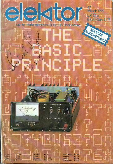
Electronics, as a hobby,used to be purelyhardware -oriented. Inrecent years, however,software is graduallycoming into the picture- as this month's coversymbolises!
contentsselektor 3-01
crosstalk canceller 3-04The weakest link in the hi-fi slain es far as crosstalk Is con-cerned is the pickup. A Japanese firm. however, has recentlyintroduced a special unit which, it is claimed, cen dramati-cally Improve the performance of cartridges In this respect.
robust lab power supply 3-08An essential of any electronics enthusiast's tab is a reliablepower
supply unit. The basic requirements for such a unit arethat it provides a fully stabilised continuously variable outputvoltage and should be fully protected against fault condi-tions such as output short circuits. The circuit describedmeets all above points, is both simple and inexpensive. endshould provide years of troublefree service.
ring modulator 3-14A ring modulator is a circuit which was originally employedin telecommunications systems for the modulation anddetection of transmission signals. More recently however, thering modulator hes found an interesting application in thefield of electronic music act is in fact now a common Maturein many synthesisers.
variable pulse generator oc KraftlMany digital applications require the use of a pulse generatorof which both frequency and duty -cycle are independently.viable. The frequency range extends from approx. 1 kHz to20 kHz, whilst the duty -cycle can be varied from almost 0 to10096.
eurotronicsElektor is promoting the first worldwide circuit and designidea competition for electronics enthusiasts, with over£ 10,000 worth of electronic equipment to be won. Closingdate: 31st March, 1979.
3-18
3-19
TUP/TUN/DUS/DUG 3-20
sinewave generator 3-21A sinsrwave generator whose fnsquency can be continuouslyvaried over virtually the eaudio spectrum, white beingeasy to construct and
nirerequiting no calibration. Just for good
measure Me circuit also offers the choice of a squarewaveoutput.
applikator 3-24Universal counter, type ICM 7216.
the ICU -a 'mini microprocessor 3-28Recently, Motorola have brought out a new IC, the IndustrialControl Unit, MC14500B. This is one -bit processor whichhas been specially designed for simple control applications,end is extremely easy to program. The following article takesa look at this 'minr-microprocessor, which should prove ofparticular interest to those readers who have had problemsgetting to grips with its 'big brothers'.
PSUs on PCBs 3.36Building power supplies the easy way.
UK 16
market UK 16
advertiser's index UK 26
missing link'4alarmzcounter, central
Supplement:BASIC (part 1), an introduction to asimple computer language.

advertisement Elektor March 1979 - UK 11
4.4
ELEKTOR
More and more4 people are reading
ElektorA recent independent survey showsthat on average 2.62 people read eachcopy of Elektor magazine each month.If you are one of the 70,000 who arenot buying your own copy butreading someone elses we would liketo draw your attention to thefollowing: -Due to our growth of circulation andpopularity of articles we find our stocks ofback issues rapidly decreasing to such anextent that very soon the only readers withall 1979 copies will be those who purchasedtheirs on publication.
However, it is still possible to avoid this bytaking out a subscription now for the rest ofthe year. Of course there are many othergood reasons for subscribing not to mentionthe fact that you would receive your owncopy prior to general availability and if youare new to Elektor a subscription for thewhole of 1979entitles you to a copy ofevery issue published so far this year atreduced prices.A post paid order form is detailed overleaffor your convenience.
SOY SIC eS4FEEEEEMEE's1. 150 100. Tremolos 1. 25. 100+ TTL 1. 26. 100+
42143 .90 .82 .69 TIP41/4 .51 .46 .39 7400 .16 .15 .1380149 .96 .86 .72 TIP41C .67 .52 .44 7401 .19 .17 .1480106 2.16 1.96 1.65 TIP42/4/8 .53 .48 .40 7401AN .21 .19 .16A1011041.1113
2.062.06
1.891.89
1.591.59
TIP42CTIP47
.571.45
.521.32
.441.11
74027403
.16
.19.15.17
.13
.149C107/4/8 .12 .11 .096 T1P48 1.54 1.39 1.17 7404 .16 .139C1013/4/1 .12 .11 .096 TIP110 1.00 .92 77 7405 .20 .18 .159C108C .13 .115 .10 TIP111 1.05 .95 .80 7406/7 .27 .24 .2111C100/4/8 .12 .11 .096 TIP112 1.20 1.10 .92 7408 .16 .15 .13BC1 03C .13 .116 .10 TIP115 1.02 .92 .78 7409 .20 .18 .1560142 .26 .24 .20 TIP116 1.07 .96 .81 7410 .16 .15 .1380143 .29 .26 .22 T1P117 1.24 1.13 .95 7412 .20 .18 .166C1824/8 .07 .06 .066 TIP120 1.03 93 .78 741245 .22 20 .1780182L .10 .075 TIP121 1.06 .96 80 7413 .32 .29 .254101133/4/6/C .07 .06 .066 TIP125 1.02 .92 .78 7016/7 .24 22 .198C18413/C .07 .06 .055 TIP126 1.07 .98 .81 7420 .16 .15 .139C1134L .10 .09 .076 TIP127 1.24 1.13 .95 7422/3 .20 AB .16902124/8 .07 .065 .065 TI P2956 .62 .67 .48 7426/6/7/8 .21 .19 .1680212E .10 .09 .075 TIP3055 .62 .57 .41 7430 .16 .15 .1341C2134J8/C .07 .065 .06 251132 .26 NU .20 7432 .11 .16 .148021413/C .07 .085 .05 252102 .38 .31 .29 7433 .23 .21 .1811/2214L .10 .09 .071 152218/4 21 .24 28 7437/8 .20 .18 .189C3013/1/380337
.25
.0923.08
.20
.086282219/A282221/A
.24
.17.21.16
.18
.1374407441/AN
.16
.74.1587
.12
.6680441 .29 .27 .22 252222/4 .15 .31 .12 7442 .28 21 .2180461 .30 .27 .23 2N2W6 41 79 :a 7443 .44 .40 .339C546/8/9/7 .07 .06 .066 262904/5 .24 .21 .18 7444 .48 .40 .3419:1130/6/7 .07 .055 2142904A/5A .26 22 .19 7445 .21 .19 .1680551179/60 .07 .065 .056 2192906/7 .15 .11 .12 7446 .50 .45 .3890970 .18 .16 .135 21429074 .16 .15 .12 7447 .40 .36 .3080131 .39 .26 .30 2143053 .23 .20 .17 7448 .50 .45 .388013210142
.40
.88.37.80
.31
.672530547143056
.67
.68.50.61
.51
.627450/1/37454/60
.19
.19.17.17
.16
.1510220/1 .45 .40 .34 253232 .83 .76 .64 7470/2 .34 .3010122 .47 .42 ,36 2143440 .80 .73 .61 7473/4 .26 .23
.36
.209132=4 .49 .44 .37 253442 1.43 1.30 1.09 1475 .21 .191001111 .32 .29 .24 2142703 .08 .07 .06 7476 .31 .28
.16
93263 .11 .30 .26 763704/5/6 .09 .08 .085 7480 .36 .33.232710341
102425-343- ' :64
i , 51SF 3898237884354018F-4 SW. 1,-..167- ' =OF 434 5.590 LE- 15
.32
.37
.42
.45
.26
.27
.28
.27
.19
.19
.23
.24
.25
.29
.33
.38
.40
.23
.24
.25
.24,I8.18.21.21.31
.24
.28
.32
.34
.20
.20
.21
.20
.15
.15
.18
.18
.19
2537712103772253773253904/6214403621440372N5294255296255298255415265416255490256492
2.062.083.45
.08
.26
.25
.46.40.49
1.081.39
.58
.61
1.871.8931.2.07.23.22.42.37
.971.26
.52
.56
1.571.592.63.08.20.19.3521
.821.06.44.48
7481127483/4847485748674897490174914570927493749474957496
.57
.31
.46
.47
.202.42
.20
.20
.31
.20
.40
.23
.34
.52
.28
.40
.42
.182.19.18.18.28.18.36.21.31
.44
.23
.34
.38
.151.86.15.15.24.15.30.18.26
- 25+.5'VAC-14337310.11',MC
.33
.3338343338x
.30
.32
.36
.3122.35.32
.25
.27
.29
.28
.272927
2145494255496214609821460992661014036640406
.84803.586860.40
.68.59.53.53.64.36.37
.49
.50
.46
.45
.48
.30
.32
749774100/47410574107/97411074111/1674118
1.02.71.86.36.42.27.89
.94
.65
.78
.32
.38
.2501
79.56.99.27.32.21.68
-ipr.de790712"WNW.-*MC
3435
31511
.3322.32.35
.2927.2729
404074041140694
.41
.41
.681.18
.37
.801.08
.32
.68
.90
74119/20741217412274123/5/6
.60.39.44.42
54.35.40.38
.48
.30
.34
.32
TTL 1. 25. 100+
74128 .45 .40 .3474132 .60 .55 .4874136 .24 .22 .18/413774141
.25
.2423.22
.19
.1874142 1.48 1.33 1.1374145 .36 .33 .17/414/ 71 .66 .5574148 .74 .67 .57/4150 .46 .40 .3474151.3 .29 .26 .2274154 .69 .63 .5374155 .28 .26 .2174156 .36 .33 .2774157 .29 .26 .2274159 .77 .70 .59741601 .38 .33 .2774162 .40 .36 .3174163/4,5 .36 .33 .27/4166 .4074167 1.26 1.14 .9774170 1.08 .99 .13370172 2.07 1.87 1.5874173 .71 .65 -5574174 .54 49 .4274175 .84 .76 .6474176/7 .2974180 .40 .36 .3074181 .99 .90 .7674182 .40 36 .3074184/5 .94 .85 .7274188AN 4.08 3.69 3.1174190/1 .31 .28 2474192/3 .36 33 .2874194 .50 .45 3874195 .27 .24 .2174196/7 .38 .35 .2974198 .60 .54 .4674198 .77 .77 .2874211741400
.91
.28.8226
.69
.22741406 .32 .29 .25741410/11 .29 .25 .2274142074510
.39
.3121328
.2224
CMOS 1+ 25. 100.
4004 .19 .175 .1540014 .19 .175 .164011/128 .19 .175 .1540138 .83 .75 .634014A .96 .86 .7240174 1.03 .92 .7940188 1.18 1.06 .204021/224 1.03 .92 .794023A .19 .18 .1640248 .93 .81 .7140254 .19 .175 .1640278 .4940288 84 .76 .6440294 1.20 1.08 924030A .45 40 .344040A 1.18 1.08 .9040428 98 .78 .664043/448 .80 .73 .6140494 .44 .40 .3440508 .44 .40 .3440518 1.24 1.12 .954068/698 .19 .175 .1540718 .19 .175 .1540988 1.67 1.51 1.28416011/2 1.04 .94 .13041758 1.23 1.11 .9441948 1.24 1.12 .944409P 6.64 6.00 5.064433P 8.73 7.90 6.654450P 3.48 3.15 2.664501CP 28 .23 .2045074 .44 .40 .3445068 .74 67 .56
DI L Sockets.
8 pm .13 .115 .09514 pm .14 .125 .10616 pin .16 .14 .1218 pm .22 .196 .16520 pin .23 .21 .1822 pin .25 .226 .1924 pin .26 .235 .2028 pin .34 .31 .2840 pin .49 .44 27
1/01119. Rya.1. 25 100+
7805 .78 .71 607812 .78 .71 .807906 .90 .82 .697912 .90 .82 .69Theo T0220
2A 100v . .411A 200v .46 .422A 400v .50 .456A 100v .51 .446A 200.. .52 .476A 400, .56 .61
10A 100v .82 .7410A 200v .84 .7610A 400+ .91 .12ThyriOors. 10220
3A 504 .37 .34 .2834 400v .41 .37 .3154 100+ .37 .34 285A 600, .60 .45 .387A 400v .56 .51 .43
10A 200v .62 .56 .48LEDs111209 .17 .156 .13TIL212 21 .19 .16T1L216 .21 .119 .16T1L220 .16 .14 .12T1L228 .23 .21 .125T1L234 .23 .21 .176TIL232 .21 .19 .16
Dodo,N914 .03 .015 .013N916 .03 .016 .01454001 .045 .04 .03554002 .05 04 .03554003 .066 .045 .0454004 .055 .06 .0454005 .065 .05 .0454005 .06 .06 .04664007 086 .055 MS64148 .03 .015 01364149 .03 .016 .014
82Y88C Soo.07 056 .047
Linear ICI, 1+ 25+ 100.
555 .30 .27 .22709 .42 .38 .32710 .47 .42 .36741 .24 .21 .18747 .40 .37 31
748CA31306
.42
.95.38.86
.32
.7231301 1.03 .94 .791-143014 .28 .25 .21
MC1310P 1.36 1.22 1.03NE555 .28 .25 .21
NE656 .51 .46 .390576003 2.20 2.00 1.68S576013 1.47 1.33 1.125676023 1.47 1.33 1.125576033 2.20 2.00 1.68U4703C .38 .36 29UA741CP .28 .25 .21
04747C .68 .61 .62U4748C .38 .35 .29TAA570 2.14 194 1.6419412060T845200
.912.04
.821.86
.691.58
1845300 1.79 1.62 1.361845400 1.92 1.73 1.46764550018856000
2.292.36
2.082.13
1.751.60
T11475007848000
1.791.79
1.621.62
1.361.38
184920 2.42 2.19 1.84T849203 2.42 2.19 1.84784950T 849900
2.292.04
2.081.85
1.751.56
TCA2700 1.79 1.62 1.36TCA800 2.82 2.55 2.15
DO Caroni. 30v
01, .022, .04 /uF .06 .05 .045.07 .06
Resistors 5 wattGarbo,' Film 5% .01 .015 .009
And many More send SAE for full listVat 811, Add 30p for P & P
We °perste a mixed pricing syriern Onsemiconductors of the same group.Example. 10 x 7400, 10 x 7411, 30.
7412,50 x 74156 + 100 itemsYou will be charged to 1001 plc..Gears Welcome, all components new endto lull spec.
Telenhpne 0822 5139. Telex 45263
Ali prices are in Es. Exchange Flame
French Fr.Belvim Fr.Dutch GuildsGorman Her k
X8.6058.5X4.1X3.8
STRUTElectrical a Mechanical Engineering Ltd
3C, Barley Market St.,Tavistock, Devon. PL19 05FTel. 0822 5439 Telex 45263
selektor elektor march 1979 - 3-01
Printed passive components.1 new method of producing capacitors,coils and resistors on foil has beendeveloped by Siemens. Introduced as*Sicufol' circuits, these passivecomponents are produced as flat zones.The rectangular, spiral and meandrousshapes of these zones and the materialused determine the capacitances,inductances and resistances. The firstmodules produced with thistechnology were used in television sets.The `Sicufor principle is based onplastic foils made of polyimide orTeflon, which are first coated withcopper in webs with lengths of severalhundred meters. Chrome -nickel layersare then deposited, from whichcapacitors and resistors are laterproduced. The windings of the coils areetched directly out of the copper layer.The passive circuits formed next to eachother on the webs in this way are cutoff to produce finished modules.Protective layers made of insulatingmaterial provide both protection andreinforcement.In contrast to conventional circuitboard technology, the components aredeposited on both sides of the actualcarrier, the plastic webs being coated onboth sides with Cu and Cr-Ni. Externalancillary devices such as potentiometers,filters and active integrated circuits aresubsequently inserted; their contacts
SICUFOLS -H1111
a
already constitute part of the finished`Sicufor circuits.The designers have paid particularattention to very close tolerances of therestance variations with temperatureand climatic conditions. It is claimedthat the fluctuations measured arewithout exception under 0.5%. The-.ernperature coefficient determining themechanical strength is lowest for adoomium content of between 53% and
ileef- and on the average less thanppm/K. Layers comprising 20%
Jamanium and 80% nickel have a
temperature coefficient of 600 ppm/K.The users of `Sicufor circuits have attheir disposal a noteworthy range ofR, C and L ratings. Surface resistancesof between 20 and 300 ohm arepossible, the resistance can be increased3800 -fold by using meanders. The loadcarrying capacity is 0.5 W/cm2.Capacitors with a polyimide carrier foilas dielectric have a surface capacitanceof 150 pF/cm2. Finally, inductances ofup to 10 pH can be produced using twospiral structures positioned directly oneabove the other on each side of the foil.Such an arrangement quadruples theinductance.The low thickness of the insulatingplastic carrier permits a variety ofthrough -plating methods, which cangreatly facilitate the accommodation ofnew circuit designs. Furthermore,conductors made of copper can besoldered, even in a flow solder bathjust like circuit boards if a polyimidefoil is used (300°C permanent tempera-ture stability). The solderability and theadditional reinforcement ensure thatthe components customary in circuitboard technology can also be usedwithout restriction for `Sicufol' circuits.Siemens AGZentralstelle fur InformationPostfach 103D-8000 Miinchen 1Federal Republic of Germany (385 S)
Energy from spaceHowever much like science fiction itmay sound, giant solar space powerstations providing energy for domesticand industrial uses on Earth may bepossible. If pilot studies to developsolar arrays into space power sourcesprove economically feasible, then bythe end of the century giant orbitingsolar power stations could be in use.Covering many miles, these would beconstructed in space from basic unitsand materials transported from Earthby advanced launch vehicles. By usingsolar cells which convert the sun'srays to electrical energy, the largearrays of today will, over the nextdecades, emerge as the early steppingstones which could lead to theutilisation of space initiated by theforthcoming Space Shuttle era.Under contract to the European SpaceAgency, Dynamics Group Electronicand Space Systems organisation atBristol are already designing the huge33 sq. metre (365 sq. ft.) 4 kW solararray that will power a space telescopefor NASA. A 6 kW lightweight flexiblefold -out array is also being developedfor communication satellites of thenext decade and proposals are in hand
to augment the Space Shuttle powerusing solar power modules of up to60 kW. Other proposals exist to developarrays up to 500 kW as space powersources. These could form modules forfurther development up to 2 MW toprovide a space power station pilotscheme which, if proved economicallyfeasible, would provide a basic sourceof energy for use on Earth.British Aerospace Dynamics Group,Filton House,Bristol,England.
(439 SI
Desirable residence for sale`Situated in El Salvador in pleasantsurroundings, modern detached fullyequipped batchelor quarters withexcellent facilities. Having an unusualroof design and an exceptionally goodreception area, would suit a radio orelectronics enthusiast. £ 6,000,000'.Actually, El Salvador, the smallest ofthe American states is the owner of thiscommunications satellite ground
station. Its 32 metre diameterparabolic antenna is operating telephoneand telex, both data and pictures,through 120 channels, to NorthAmerica and Europe via the IntelsatIV -A satellite. It is capable of beingextended although some of thechannels now being used are leased toneighbouring countries. The installation,built by Siemens of West Germany,was completed and operational in 18months at a cost of 23 million DM.
(437 S)
3-02 - elektor march 1979 selektor
Laser gyroFerranti are to develop a laser gyro andto incorporate it in an experimentalmodel of a strap -down inertialnavigation system.The aim is, first, to produce a systemfor installation in transport aircraft,followed, if tests and trials aresatisfactory, by the development of alaser -gyro navigator for combataircraft.Interest in the laser gyro exists because,potentially, it could provide a morerobust and mechanically simpler devicefor detecting movement than theexisting spinning -mass gyro employedtoday. Because of the greatersimplicity it is also expected that thetotal cost of ownership (initial capitalcost plus maintenance costs) of alaser -gyro inertial navigation systemthroughout its service life would bemuch less than the equivalentconventional gimbal gyro system.Currently the Ferranti Inertial SystemsDepartment has developed a gimbal -supported inertial platformincorporating conventional spinning -mass gyros. However, a simpler methodof sensing motion would be toeliminate the gimbal support and mountthe gyros permanently in a fixed -position - the so-called 'strap -down'configuration. In a gimbal system theplatform is always maintained in a fixedorientation in space - the datumreference position. With a strap -downsystem the displacement of the gyrowith respect to the starting datum isassessed and stored by a computerassociated with the system.The problem with the strap -downmethod is that the gyros used have tobe mechanically robust and continue toperform with great accuracy even whensubject to increased vibration and thehigher angular and linear rates ofaccelerations implicit in being 'strapped-
ATI LEN0114C01471104. MIRROR
110. MNTAXIS
down'. The spinning -mass gyros in thecurrent designs of inertial platform areshielded to a considerable extent fromthese harsh conditions by virtue ofbeing gimbal supported.The laser gyro, if it can be made towork with sufficient accuracy, offers asolution to this problem because it hasno moving parts and is of ruggedconstruction.
Principle of the laser gyro
The type of laser gyro Ferranti isdeveloping is triangular in plan. Itcomprises a single block of vitreousceramic material in which three cavitiesof circular cross-section have beendrilled. The three cavities form atriangle in one plane. A mirror ispositioned at the angular junctionbetween each pair of cavities. Thevitreous ceramic selected has a lowtemperature coefficient of expansionto ensure the mirrors remainaccurately aligned with the cavitiesunder all operational conditions.The cavities are filled with a lasingmaterial and Ferranti have selected ahelium neon gas mixture for thispurpose. A cathode is situatedmidway along the length of one cavityand anodes are positioned towards thefurthermost ends in the two remainingcavities. The helium neon mixture isexcited to lase by electrical dischargesoccurring between the cathode and thetwo anodes. As a result, twoindependent coherent electromagneticwaves are generated - one travellinground the triangular resonating cavityin a clockwise direction, and the otherin a counter -clockwise direction.If the assembly is now spun about avertical axis perpendicular to the planeof the cavities the effective patharound which one electromagneticwave is travelling will appear tolengthen, and the other to shorten. To
CURVED MIRROR
a detector placed at one of thereflecting mirrors the frequency of theelectromagnetic wave propagated in onedirection will appear to increase whilethat of the other wave will decrease.The difference in frequency betweenthe two waves is directly proportionalto the rate of rotation of the chamberabout its perpendicular axis. Thedetector produces output pulses at afrequency proportional to the rate ofrotation. Angular rates of accelerationcan be determined by assessing changesin output pulse frequency. This devicehas all the characteristics of a gyro -hence the laser gyro.The major technical problems that haveto be solved before the laser gyrobecomes a practical proposition are:a) the generation of a truly linear
output signal at extremely lowrates of angular rotation (the twowave patterns tend to 'locktogether' under these conditions)
andb) to devise manufacturing techniques
that enable the required highaccuracies to be consistentlyachieved and maintained on aproduction basis.
Should the results attained in the newdevelopment programme besatisfactory it is expected that, fromthe mid to late 1980s onwards, lasergyros incorporated in `strap -down'systems will be specified for manyairborne applications.Inertial Systems Department,Ferranti Limited,Silverknowes,Ferry Road,Edinburgh, EH4 4AD.
(440 Sl
RCA enter the video disc marketVideo recording is probably thebiggest new innovation in homeentertainment since the colourtelevision and RCA are not alone intheir view that video discs will be amulti -million dollar business in the1980's. This company plan to achievethe earliest possible wide scaledistribution of their `Selecta Vision'video disc in the United States. TheRCA system uses a grooved disc that isplayed with a diamond stylus at 450revolutions per minute and contains onehour of programme per side. The playeris designed for use with any televisionset, keeping the overall cost to aminimum. An unusual feature is theplastic sleeve resembling a record albumcover, which deposits the disc on theturntable when inserted into a slot onthe front of the machine. The disc is
selektor elektor march 1979 - 3-03
I
removed by reinserting the emptysleeve back into the player. In thissystem the sleeve is a protectionagainst environmental hazards such aswarping, dust and scratches and alsoprevents the disc being touched byhand. RCA's initial catalogue willcontain 250 titles, including featuremotion pictures, as well as childrens,how-to, sports, cultural, educationaland musical programmes.RCA International Ltd.RCA House,50, Curzon Street,London, WI Y 8EUEngland.
(438 S)
AP -control for church organA microprocessor register controlsystem has recently been fitted to theorgan in the 600 year old St. LorenzChurch in Nuremberg. The system,known as the `Registronik', wasspecially developed for the 138 -registerorgan by two engineers of SiemensGeratewerk, Erlangen. Up to fortyregister combinations can be stored forinstant recall, so that the stops requiredfor different pieces of music can beset before the performance. Wholerecitals or the entire music for a churchservice can be preprogrammed in thisway, leaving the organist free tooperate the manuals and pedals sothat he can give his full attention to the
music itself. The control system is avery compact design, the stop keysbeing grouped together on a panel nolarger than a notebook. The associatedelectronics are accomodated in asmall metal cabinet in an adjoiningroom. The organ was previouslyequipped with an electromechanicalfour -combination register controlsystem and, using conventionalmethods, forty combinations wouldhave required more space than the restof the organ. The organ which, exceptfor the Passau organ, is the largest inthe Federal Republic of Germanywill certainly attract many people toNuremberg.
(441 SI
Little LA new range of ceramic chip inductors,available from Steatite Insulations Ltd,will not pass through the eye of a needlebut the dimensions are sufficiently smallfor these electronics components to beused in thick film switch circuits.These miniature ceramic chip inductorsare an entirely new developmentdesigned for hybrid technology with afixed inductance. With nominal dimen-sions of only 2.5 mm x 2.5 mm x 1.9 mm,they have inductance ranges fromapproximately 4 nH to I AH, withtolerances of ± 5 and 10%.
The coil winding is applied as a singlelayer and a new process has beendeveloped so that the winding endscan be welded to metallised surfaceterminals on the ceramic body. Theycan also be soldered together with othercomponents and are claimed to beimpervious to attack from all generalcleaning fluids.Higher inductance units are currentlyunder development utilising magneticbodies together with variable inductancecomponents.Steatite Insulations Ltd.,Hagley House,Hagley Road,Birmingham,B16 8QW,England
(442 S)
A11-ElecironiceSnow
3s ElectronicsLtd
344- 36 High Street
SeftonWalden
SahronWalden
22612/27137Essex'Telephone:
Telex. 61663
vnat
nice
Are microprocessors nasty?Apparently, microprocessors are nastythings - or so one would assume fromthe amusing title of a recent pressrelease! However, the organisers of theAll Electronics Show are also makingevery effort to bring the manufacturesand potential users into (hopefullyprofitable) contact.A unique gathering .A unique gathering of the manufacturesof microprocessors (or 'chips', as theyare familiarly known) has been arrangedin the West End of London at which,free of charge, visitors may discuss howthis new technology will affect them.Among those present are TexasInstruments, who invented theintegrated circuit, and Fairchild Semi-conductor who are now seen as thetechnology leaders.The organisers of the event (The All -Electronics Show at Grosvenor Housein Park Lane between 27th Februaryand 1st March) claim that there is nowvirtually no industry in Britain whichwill not be affected by microprocessors.They add that every director and seniormanager of a company manufacturinganything should get face-to-face withthe manufacturers and distributors of atechnology which the Government issupporting to the tune of £ 70 million
If you would like to ask even the mostbasic of questions, just send a stampand addressed envelope to Sam Clarke,Dept. 3, 34-36 High Street, SaffronWalden, Essex and a free admissionticket - together with a special listingof the appropriate exhibitors - willbe sent to you.The All -Electronics Show,Ars Electronica Ltd.,34-36 High Street,Saffron Walden Essex
like micro
ublicationlike
this?
P. uniquegathering
of
(or 'chips,as they
are f
in the
of London
WestEnd
-how this
new
ftvdiscuss
-*
a
r essordoin
in a
(443 S)
microprocessors
the manufacturers
of
amiliarlyknown)
has beenarranged
harge,visitors
at which,free
of c
them.
technologywill
affect
are TexasInstruments,
who invented
-4-,.torwho are
3-04 - elektor march 1979 crosstalk canceller
crosstalkcancellerSeparating left from right.
The weakest link in the hi-fi chainas far as crosstalk is concerned isthe pickup. A Japanese firm,however, has recently introduceda special unit which, it is claimed,can dramatically improve theperformance of cartridges in thisrespect. The following articletakes a look at this interestingdevelopment.
Stereo reproduction has been with usnow for a good twenty years or so,and the principles involved are well-known. Two separate sound channelsare modulated in two different planesin the grooves of a disc. This 'left andright channel' information must be fedthrough separate amplifier channels toseparate loudspeakers. If this isachieved, the result is more or lessaccurate 'positioning' of individualinstruments within an overall soundimage or stereo 'picture' as it is called(see figure 1). The position of a par-ticular instrument, or of vocals, withinthe stereo image is determined by theproportion (and phase) of the cone-sponding electrical signal present ineach channel. The greater the differencein signal strength, the more the resulting
sound will appear to be shifted towardsthe loudspeaker of the channel where itis strongest.
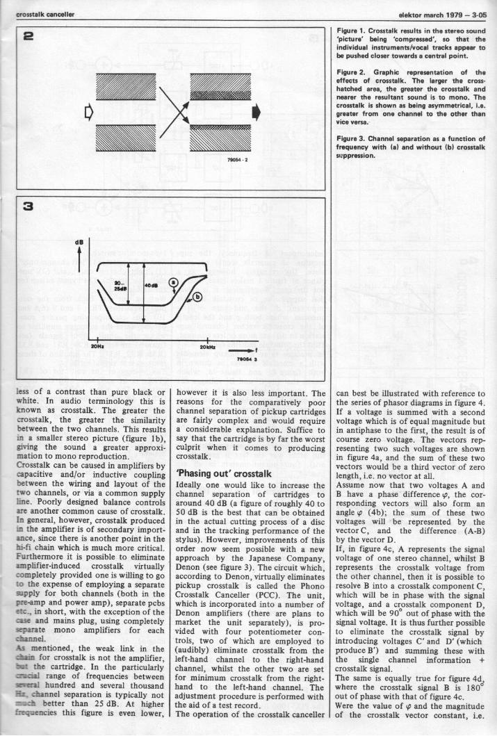
Talking about crosstalkIn the ideal situation the left and rightchannel information is only combinedas the output sound waves of the twoloudspeakers encounter one another inthe listening room. In practice, however,it is unfortunately the case that neitherchannel is completely free of some smallpart of the other channel. The effect ofthis is to reduce the differences betweenthe two channels so that they tend tosound more similar. As figure 2 illus-trates, the process is analogous tomixing a touch of black with a whitepaint and vice versa. The result is alight and dark grey, which provide much
crosstalk canceller elektor march 1979 - 3-05
2
78064 - 2
less of a contrast than pure black orwhite. In audio terminology this isknown as crosstalk. The greater thecrosstalk, the greater the similaritybetween the two channels. This resultsin a smaller stereo picture (figure I b),giving the sound a greater approxi-mation to mono reproduction.Crosstalk can be caused in amplifiers by
pacitive and/or inductive couplingbetween the wiring and layout of thetwo channels, or via a common supplyline. Poorly designed balance controlsare another common cause of crosstalk.In general, however, crosstalk producedin the amplifier is of secondary import-ance, since there is another point in thehi-fi chain which is much more critical.Furthermore it is possible to eliminateamplifier -induced crosstalk virtuallycompletely provided one is willing to goto the expense of employing a separateamply for both channels (both in thepre -amp and power amp), separate pcbsetc.. in short, with the exception of the=se and mains plug, using completelyseparate mono amplifiers for eachchannel.As mentioned, the weak link in thechain for crosstalk is not the amplifier,bat the cartridge. In the particularlymacial range of frequencies betweenseveral hundred and several thousandHi. channel separation is typically not
better than 25 dB. At higherfre..;_:encies this figure is even lower,
however it is also less important. Thereasons for the comparatively poorchannel separation of pickup cartridgesare fairly complex and would requirea considerable explanation. Suffice tosay that the cartridge is by far the worstculprit when it comes to producingcrosstalk.
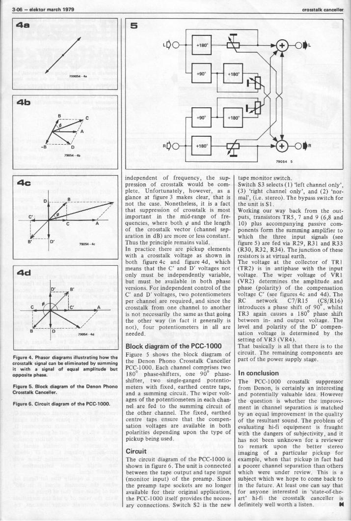
'Phasing out' crosstalkIdeally one would like to increase thechannel separation of cartridges toaround 40 dB (a figure of roughly 40 to50 dB is the best that can be obtainedin the actual cutting process of a discand in the tracking performance of thestylus). However, improvements of thisorder now seem possible with a newapproach by the Japanese Company,Denon (see figure 3). The circuit which,according to Denon, virtually eliminatespickup crosstalk is called the PhonoCrosstalk Canceller (PCC). The unit,which is incorporated into a number ofDenon amplifiers (there are plans tomarket the unit separately), is pro-vided with four potentiometer con-trols, two of which are employed to(audibly) eliminate crosstalk from theleft-hand channel to the right-handchannel, whilst the other two are setfor minimum crosstalk from the right-hand to the left-hand channel. Theadjustment procedure is performed withthe aid of a test record.The operation of the crosstalk canceller
Figure 1. Crosstalk results in the stereo sound'picture' being 'compressed', so that theindividual instruments/vocal tracks appear tobe pushed closer towards a central point.
Figure 2. Graphic representation of theeffects of crosstalk. The larger the cross-hatched area, the greater the crosstalk andnearer the resultant sound is to mono. Thecrosstalk is shown as being asymmetrical, i.e.greater from one channel to the other thanvice versa.
Figure 3. Channel separation as a function offrequency with la/ and without lb/ crosstalksuppression.
can best be illustrated with reference tothe series of phasor diagrams in figure 4.If a voltage is summed with a secondvoltage which is of equal magnitude butin antiphase to the first, the result is ofcourse zero voltage. The vectors rep-resenting two such voltages are shownin figure 4a, and the sum of these twovectors would be a third vector of zerolength, i.e. no vector at all.Assume now that two voltages A andB have a phase difference tp, the cor-responding vectors will also form anangle tp (4b); the sum of these twovoltages will be represented by thevector C, and the difference (A -B)by the vector D.If, in figure 4c, A represents the signalvoltage of one stereo channel, whilst Brepresents the crosstalk voltage fromthe other channel, then it is possible toresolve B into a crosstalk component C,which will be in phase with the signalvoltage, and a crosstalk component D,which will be 90° out of phase with thesignal voltage. It is thus further possibleto eliminate the crosstalk signal byintroducing voltages C' and D' (whichproduce B') and summing these withthe single channel information +crosstalk signal.The same is equally true for figure 4dewhere the crosstalk signal B is 180aout of phase with that of figure 4c.Were the value of kp and the magnitudeof the crosstalk vector constant, i.e.
3-06 - elektor march 1979 crosstalk canceller
4a
799056. a
Figure 4. Phasor diagrams illustrating how thecrosstalk signal can be eliminated by summingit with a signal of equal amplitude butopposite phase.
Figure 5. Block diagram of the Denon PhonoCrosstalk Canceller.
Figure 6. Circuit diagram of the PCC-1000.
independent of frequency, the sup-pression of crosstalk would be com-plete. Unfortunately, however, as aglance at figure 3 makes clear, that isnot the case. Nonetheless, it is a factthat suppression of crosstalk is mostimportant in the mid -range of fre-quencies, where both Li, and the lengthof the crosstalk vector (channel sep-aration in dB) are more or less constant.Thus the principle remains valid.In practice there are pickup elementswith a crosstalk voltage as shown inboth figure 4c and figure 4d, whichmeans that the C' and D' voltages notonly must be independently variable,but must be available in both phaseversions. For independent control of theC' and D' voltages, two potentiometersper channel are required, and since thecrosstalk from one channel to anotheris not necessarily the same as that goingthe other way (in fact it generally isnot), four potentiometers in all areneeded.
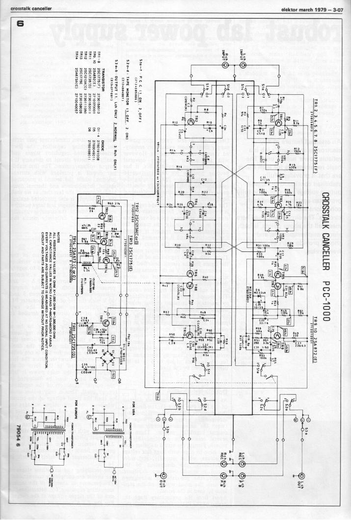
Block diagram of the PCC-1000Figure 5 shows the block diagram ofthe Denon Phono Crosstalk CancellerPCC-1000. Each channel comprises two180° phase -shifters, one 90° phase -shifter, two single -ganged potentio-meters with fixed, earthed centre taps,and a summing circuit. The wiper volt-ages of the potentiometers in each chan-nel are fed to the summing circuit ofthe other channel. The fixed, earthedcentre taps ensure that the compen-sation voltages are available in bothpolarities depending upon the type ofpickup being used.
CircuitThe circuit diagram of the PCC-1000 isshown in figure 6. The unit is connectedbetween the tape output and tape input(monitor input) of the preamp. Sincethe preamp tape sockets are no longeravailable for their original application,the PCC-1000 itself provides the necess-ary connections. Switch S2 is the new
tape monitor switch.Switch S3 selects (I) 'left channel only',(3) 'right channel only', and (2) 'nor-mal', (i.e. stereo). The bypass switch forthe unit is S 1.Working our way back from the out-puts, transistors TR5, 7 and 9 (6,8 and10) plus accompanying passive com-ponents form the summing amplifier towhich the three input signals (seefigure 5) are fed via R29, R31 and R33(R30, R32, R34). The junction of theseresistors is at virtual earth.The voltage at the collector of TR I(TR2) is in antiphase with the inputvoltage. The wiper voltage of VR1(VR2) determines the amplitude andphase (polarity) of the compensationvoltage C' (see figures 4c and 4d). TheRC network C7/R15 (C8/R16)introduces a phase shift of 90°, whilstTR3 again causes a 180° phase shiftbetween in- and output voltage. Thelevel and polarity of the D' compen-sation voltage is determined by thesetting of VR3 (VR4).That basically is all that there is to thecircuit. The remaining components arcpart of the power supply stage.
In conclusionThe PCC-1000 crosstalk suppressorfrom Denon, is certainly an interestingand potentially valuable idea. Howeverthe question is whether the improve-ment in channel separation is matchedby an equal improvement in the qualityof the resultant sound. The problem ofevaluating hi-fi equipment is fraughtwith the dangers of subjectivity, and ithas not been unknown for a reviewerto remark upon the better stereoimaging of a particular pickup forexample, when that pickup in fact hada poorer channel separation than otherswhich were under review. This is asubject which we hope to come back toin the future. At least one can say thatfor anyone interested in 'state-of-the-art' hi-fi the crosstalk canceller isdefinitely well worth a listen.
8CY
O
LchIN
PU
T
Rch
INP
UT
TR
1. 2 . 3.4.5.6.7. 6: 25C1775(F
)
CR
OS
ST
ALK
CA
NC
ELLE
RP
C C
-10 0 0TR
9.10: 25A872 (E
)2 %
%%
%%
00121710070001
06;
Sla-t
P C
C11
ON
. 2,OF
F)
121220 OO
OO
O 1
5 2 o-cl,
TA
PE
MO
NIT
OR
11 OF
F .
2O
NI
doC
013003
12121001007
531-e = O
UT
PU
T 1
1.Lclt O
NLY
(5112017001I
TR
AN
SIS
TO
R
2. NO
RM
AL
3. Rch O
NLY
I
DIO
DE
001-82S
C1775(F
)2730158013
01-42760191008
TR
9. 102S
A852(E
)2710070001
052760049011
TF
11125C
1735f0)27301830)1
062760188011
11122S
C1213A
(C)
2730111050T
0132S
C1775E
2730158026T
R14
2SA
673A(C
)2710040057
CIS
'01/3S
T R
I2 25C1213A
(CorD
)27301110S
0T
R13. 25C
1775(g_27)014)011
Cl)
CC
2SS
1.110
1330111112760020011
TR
IO: 25A
673 (C or 0)
C27 0020037 0 2710040040
12112 104
-43536
f04 00
OU
T
J.
FO
R U
SA
PO
MM
MA
MP
Om
MO
MO
01-2 MO
)C2710191000_._06
TR
11:25C1735(0)
1720113011
NO
TE
SA
LL RE
SIS
TA
NC
E V
ALU
ES
IN O
HM
K.I.0000H
M M
.1,000.000 OH
MA
LL CA
PA
CIT
AN
CE
VA
LUE
S IN
MIC
RO
FA
RA
D P
-MIC
RO
-MIC
RO
FA
RA
DE
VE
RY
VO
LTA
GE
S A
RO
CU
RR
EN
TS
IS M
EA
SU
RE
D A
T N
O S
IGN
AL IN
PU
T C
ON
DIT
ION
.C
IRC
UIT
AN
D P
AR
TS
AR
E S
UB
JEC
T T
O C
HA
NG
E W
ITH
OU
T P
RIO
R N
OT
ICE
.
3)Jv0708
FO
R E
UR
OP
EOl0
MM
OP
OP
OM
A
L CO
P. B
Rch
P. B
?Rch O
UT
MIM
01010
44.410
79054 8
3-08 - elektor march 1979 robust lab power supply
robust lab power supply
An essential feature of anyelectronics enthusiast's lab is areliable power supply unit. Thebasic requirements for such a unitare that it provides a fullystabilised continuously variableoutput voltage and should be fullyprotected against eventual faultconditions such as output shortcircuits. The circuit described heremeets all the above points, is bothsimple and inexpensive, andshould provide years of trouble -free service.
Until only a few years ago, powersupply units almost exclusively employ-ed discrete regulator circuits. Howeverwith the advent of cheap universalprecision voltage regulator ICs, it hasbecome possible for the amateur tobuild an inexpensive PSU enjoying thespecifications which previously were thepreserve of expensive professionalequipment.The basic function of a voltage regulatoris twofold. Firstly, to maintain a con-stant output voltage in spite of variationsin the input voltage (i.e. the mains). Itsperformance in this respect is termedline regulation and is expressed as thepercentage change in the input voltagewhich is passed on to the output voltage.Thus, with a line regulation of 0.1% -the figure for the circuit described here- a change of 10 V in the mains supplywill produce a variation of not morethan 0.1% of 10 V = 0.01 V in theoutput voltage of the regulator circuit.The second function of a regulator isto maintain a constant output voltagedespite variations in the current drawnby the load. Load regulation is ex-pressed as the percentage change in theoutput voltage for a specific change inthe output load current (or when theload current is varied over its completerange). Thus, in this circuit the outputvoltage will not vary by more than 1%for fluctuations of up to 5 A in thecurrent drawn by the load.
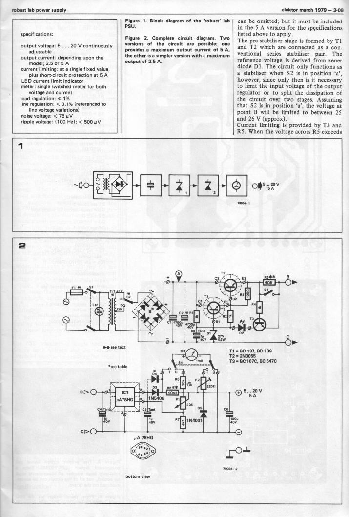
Double stabilisationAs can be seen from the block diagramof the PSU (see figure 1), the design ofthe circuit is slightly unusual in that itincorporates a pre -stabiliser stage be-tween the unregulated supply and theoutput regulator proper. There areseveral reasons for adopting this ap-proach. Firstly, the actual stabiliser doesnot have to cope with large line voltagevariations, whilst secondly, and moreimportantly, the dissipation of thecircuit is spread over two stabilisers.Finally, the pre -stabiliser is requiredto limit the input voltage of the regu-lator IC used in the circuit.Apart from the preliminary stage, thedesign of the PSU is fairly conventional:
mains step-down transformer plus recti-fier, smoothing capacitor, the twoseries -connected regulator stages andfinally, a meter circuit to measure theoutput voltage/current. The first stabil-iser circuit is provided with currentlimiting, whilst the second is protectedagainst short-circuits and thermal over-load. In view of the fact that, as we shallsee, the supply is also protected againstboth negative voltages and large positivevoltage transients, the circuit is virtually'idiot -proof and definitely merits theaccolade 'robust'.
CircuitThe complete circuit diagram of thePSU is shown in figure 2. Two versionsof the circuit - one designed to supplya maximum of 5 A, and a simplerversion which provides 2.5 A - arepresented. In both cases the outputvoltage can be varied between 5 and20 V with the aid of potentiometer P1.The differences between the twoversions of the circuit are detailed intable 1.What may initially appear to be arather curious problem with regulatorcircuits is the fact that the lower theoutput voltage, the greater the dissi-pation. The reason for this is not diffi-cult to explain however, since the lesspower 'dissipated' in the form of anoutput voltage, the more power is 'leftover' and hence must be dissipated inthe output transistors of the regulatorcircuit itself. Thus it only makes senseto limit the input voltage of the circuitwhenever only low output voltages arerequired. To this end the transformer isprovided with both 12 V and 24 Vsecondary windings which can beswitched with the aid of S2. In view ofthe lower current, the dissipation of the2.5 A version of the circuit is not aproblem, hence the secondary voltage ofthe transformer can safely be left at24 V.The rectifying and smoothing stages ofthe circuit are completely conventional.The presence or absence of the secondsmoothing capacitor, C2, determines thesize of the ripple voltage at the output.For the 2.5 A version of the circuit C2
robust lab powe supply elektor march 1979 - 3-09
specifications:
output voltage: 5 . . 20 V continuouslyadjustable
output current: depending upon themodel; 2.5 or 5 A
current limiting: at a single fixed value,plus short-circuit protection at 5 A
LED current limit indicatormeter: single switched meter for both
voltage and currentload regulation: < 1%line regulation: < 0.1% (referenced to
line voltage variations)noise voltage: < 75 µVripple voltage: (100 Hz): < 500 µV
Figure 1. Block diagram of the 'robust' labPSU.
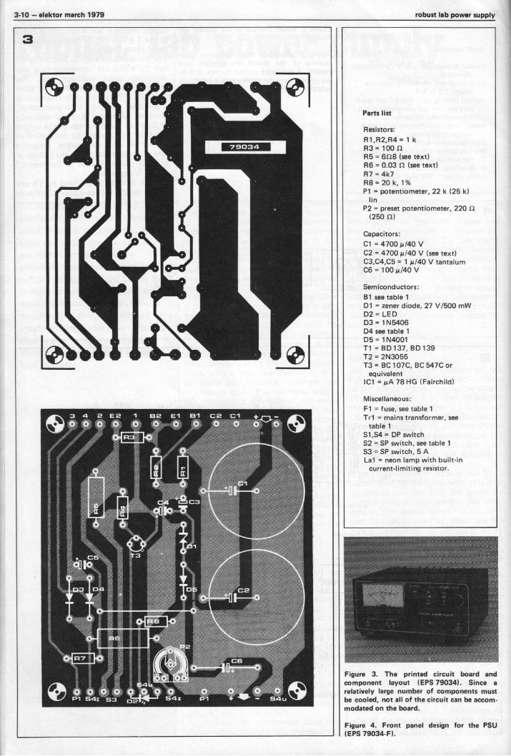
Figure 2. Complete circuit diagram. Twoversions of the circuit are possible: oneprovides a maximum output current of 5 A,the other is a simpler version with a maximumoutput of 2.5 A.
can be omitted; but it must be includedin the 5 A version for the specificationslisted above to apply.The pre -stabiliser stage is formed by TIand T2 which are connected as a con-ventional series stabiliser pair. Thereference voltage is derived from zenerdiode DI. The circuit only functions asa stabiliser when S2 is in position 'a',however, since only then is it necessaryto limit the input voltage of the outputregulator or to split the dissipation ofthe circuit over two stages. Assumingthat S2 is in position 'a', the voltage atpoint B will be limited to between 25and 26 V (approx).Current limiting is provided by T3 andR5. When the voltage across R5 exceeds
2
** see text
"see table
NA 78HG
bottom view
Ti = BD 137, BD 139T2 = 2N3055T3 = BC 107C, BC 547C
79034 - 2
5 ... 20 V5A
3-10 - elektor march 1979 robust lab power supply
Parts list
Resistors:
R1,R2,R4 = 1 kR3 = 100 E2R5 --- 6E28 (see text)R6 = 0.03 11 (see text)R7 = 4k7R8 = 20 k, 1%P1 = potentiometer, 22 k (25 k)
linP2 = preset potentiometer, 220
(250 S2)
Capacitors:C1 = 4700 /.2/40 VC2 = 4700 µ140 V (see text)C3,C4,C5 = 1 4/40 V tantalumC6 = 100 At/40 V
Semiconductors:B1 see table 1D1 = zener diode, 27 V/500 mWD2 = LEDD3 = 1 N5406D4 see table 1D5 = 1N4001T1 = BD 137, BD 139T2 = 2N3055T3 = BC 107C, BC 547C or
equivalentIC1 = ALA 78 HG (Fairchild)
Miscellaneous:F1 = fuse, see table 1Tr1 = mains transformer, see
table 1S1,S4 = DP switchS2 = SP switch, see table 1S3 = SP switch, 5 ALal = neon lamp with built-in
current -limiting resistor.
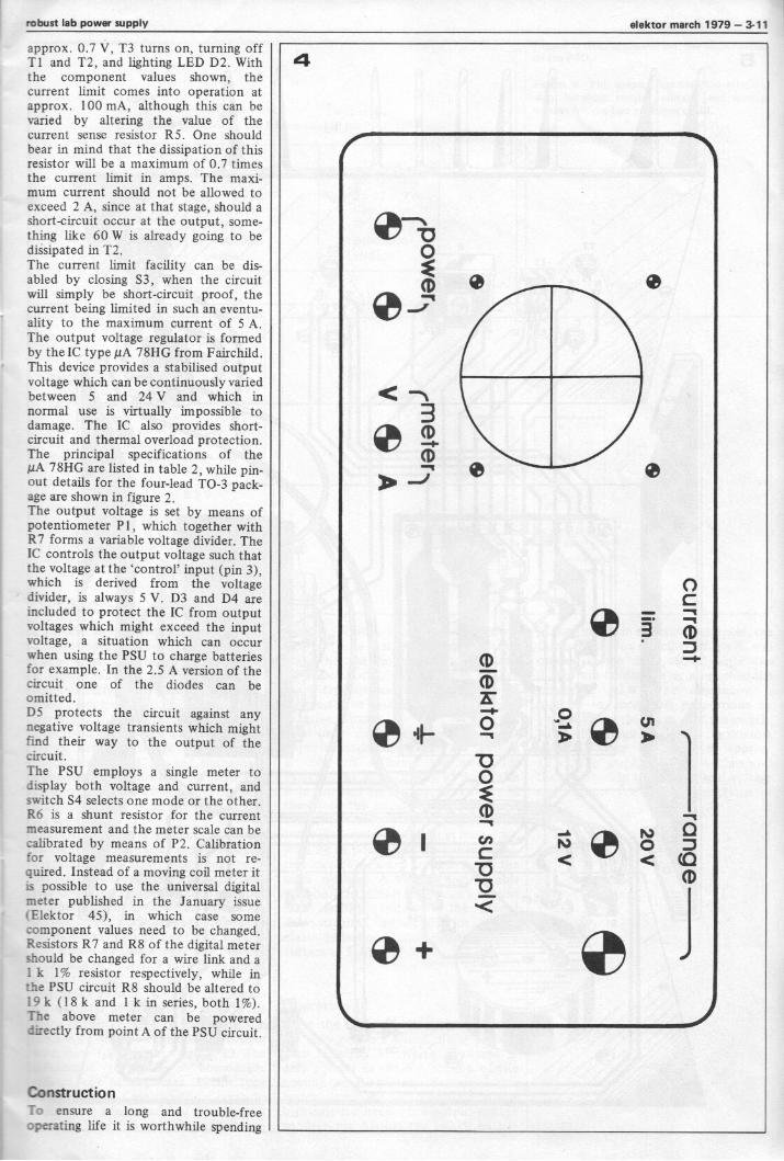
Figure 3. The printed circuit board andcomponent layout (EPS 790341. Since a
relatively large number of components mustbe cooled, not all of the circuit can be accom-modated on the board.
Figure 4. Front panel design for the PSU(EPS 79034-F).
robust lab power supply elektor march 1979 - 3-11
approx. 0.7 V, T3 turns on, turning offT1 and T2, and lighting LED D2. Withthe component values shown, thecurrent limit comes into operation atapprox. 100 mA, although this can hevaried by altering the value of thecurrent sense resistor R5. One shouldbear in mind that the dissipation of thisresistor will he a maximum of 0.7 timesthe current limit in amps. The maxi-mum current should not be allowed toexceed 2 A, since at that stage, should ashort-circuit occur at the output, some-thing like 60 W is already going to bedissipated in T2.The current limit facility can be dis-abled by closing S3, when the circuitwill simply be short-circuit proof, thecurrent being limited in such an eventu-ality to the maximum current of 5 A.The output voltage regulator is formedby the IC type µA 78HG from Fairchild.This device provides a stabilised outputvoltage which can be continuously variedbetween 5 and 24 V and which innormal use is virtually impossible todamage. The IC also provides short-circuit and thermal overload protection.The principal specifications of theµA 78HG are listed in table 2, while pin-
out details for the four -lead TO -3 pack-age are shown in figure 2.The output voltage is set by means ofpotentiometer PI, which together withR7 forms a variable voltage divider. TheIC controls the output voltage such thatthe voltage at the 'control' input (pin 3),which is derived from the voltagedivider, is always 5 V. D3 and D4 areincluded to protect the IC from outputvoltages which might exceed the inputvoltage, a situation which can occurwhen using the PSU to charge batteriesfor example. In the 2.5 A version of thecircuit one of the diodes can heomitted.D5 protects the circuit against anynegative voltage transients which mightfind their way to the output of thecircuit.The PSU employs a single meter todisplay both voltage and current, andswitch S4 selects one mode or the other.R6 is a shunt resistor for the currentmeasurement and the meter scale can becalibrated by means of P2. Calibrationfor voltage measurements is not re-quired. Instead of a moving coil meter itis possible to use the universal digitalmeter published in the January issue(Elektor 45), in which case somecomponent values need to be changed.Resistors R7 and R8 of the digital metershould be changed for a wire link and a1 k 1% resistor respectively, while inthe PSU circuit R8 should be altered to19 k (18 k and 1 k in series, both 1%).The above meter can be powereddirectly from point A of the PSU circuit.
ConstructionTo ensure a long and trouble -freeoperating life it is worthwhile spending
-
robust lab power supply elektor march 1979 - 3-13
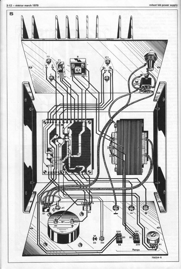
Figure 5. Wiring details for the constructionof the PSU.
Table 1.
Differences between 2.5 and 5 A versions of the PSU
2.5 A 5 AFlTr1
S2
B1
D4
250 mA fuse2 x 12 V/3.5 Atransformeromitted134062500
omitted
500 mA fuse2 x 12 V/7 AtransformerSP switch, 7 A840050001N5406
Table 2.
Specifications of µA 78HG
max. dissipation: 50 W (at 25°C)max. input voltage: 40 Vmax. voltage difference between in- and
output: 25 Vmax. current: 7 Acontrol voltage: 4.8 V ... 5.2 Vload regulation: < 1%line regulation: < 1%quiescent current: < 10 mAripple suppression: 3 60 dBnoise voltage: 75 µV
a certain amount of attention on theconstructional details of the PSU.The printed circuit board for the projectis shown in figure 3. However, since acomparatively large number of compo-nents must be cooled, most of these aremounted off -board. Particular attentionmust be given to the cooling arrange-ments for the bridge rectifier, B 1,transistors T1 and T2, and the voltageregulator, IC1. In the case of the IC, onemust reckon with a dissipation of some-thing like 50 W, hence a beefy heat sinkis a must.Similarly, adequate precautions shouldbe taken with T2, since it will dissipateanything up to 60 W. The bridge recti-fier and T1 are not quite such a problemand could be cooled by, for example,mounting them on the case. However,do not forget to electrically insulate thecomponents being cooled (mica washersand silicon grease) - with the possibleexception of ICI wich may be mountedwithout insulation.The shunt resistor, R6, will have to beself -wound. The simplest method ofdoing this is to wind 36 cm of 0.6 mm(24 s.w.g.) diameter enamelled copperwire on a 1 W resistor (e.g. 10 k). Theinductance of such a home-maderesistor can be neglected in this typeof application. Care should be taken toensure that the connecting wire is ratedto carry the full 5 A the circuit can
supply. Wiring details are shown infigure 5. Note that in contrast to normalusage the case should not be connectedto circuit earth, but rather is earthedvia a seperate socket. In this way thecircuit can be used for both positive andnegative voltages.The only component in the circuitrequiring initial adjustment is P2, whichis used to calibrate the meter forcurrent. The simplest way of doing thisis to set the PSU for, say, 10 V out, andthen load the circuit with 45 Watt carheadlamp bulb, with an ammeter inseries (full scale deflection at least 4 A).With S4 in position 'I' the meter deflec-tion can be adjusted until it shows thesame reading. A slightly less reliablemethod is to inhibit the circuit's currentlimit facility, and with the outputshort-circuited, adjust P2 for a full-scale deflection (corresponding to acurrent of 5 A).
OperationUsing the PSU is quite straightforward,the only problem which might presentitself is switch S2 (which, of course, isonly present in the 5 A version of thecircuit). As was already mentioned, thisswitch should be set to position 'b' forhigh -output -current low -output -voltageapplications. Should the switch be left
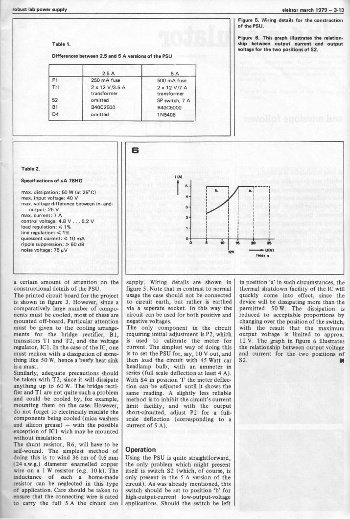
Figure 6. This graph illustrates the relation-ship between output current and outputvoltage for the two positions of S2.
in position 'a' in such circumstances, thethermal shutdown facility of the IC willquickly come into effect, since thedevice will be dissipating more than thepermitted 50 W. The dissipation isreduced to acceptable proportions bychanging over the position of the switch,with the result that the maximumoutput voltage is limited to approx.12 V. The graph in figure 6 illustratesthe relationship between output voltageand current for the two positions ofS2.
3-14 - elektor march 1979 ring modulator
ring modulator
and envelope follower
A ring modulator is a circuitwhich was originally employed intelecommunications systems forthe modulation and detection oftransmission signals. More recentlyhowever, the ring modulator hasfound an interesting application inthe field of electronic music and isin fact now a common feature inmany synthesisers.
A ring modulator is basically a fourquadrant multiplier, that is to say, acircuit which will multiply two inputvoltages, regardless of whether they arepositive or negative and ensure that theproduct voltage is of the correct po-larity. Thus a positive voltage multipliedby a negative voltage will yield anegative voltage, a negative voltagetimes a negative voltage will give apositive voltage, and so on.The question is: why is such a circuit ofinterest to the electronic music enthusi-ast? The answer can be found by con-sidering the following mathematicalexpression for the product of twosinewaves:sin a sin (3 =1/2 cos (a-/3) -1h cos (a+/3).Since a cosine is simply a sinewavewith a 900 phase shift, it can beseen that multiplying two sinewavesresults in two new sinew ave signalswhose frequencies are the sum anddifference respectively of the twooriginal signals. Note that this is onlytrue for sinewave signals and not forother types of waveform. However thesame effect will be produced by com-binations of sinewaves. Thus, forexample, if a combination of twosinewaves is multiplied with a thirdsinewave, each of the constituentsinewaves in the original signal willproduce its 'own' sum and differenceproducts. The multiplication of twosinewave input signals is illustrated inthe oscilloscope photo of figure 1. Thesinewave of the upper trace is multipliedwith a second sinewave of higher fre-quency to produce the productwaveform shown on the lower trace.
'Klangs'The most significant feature of the ringmodulator is its ability to exploit theharmonic relationship of different notes.This can best be explained with the aidof a further example. Assume that wefeed two sinewave signals with fre-quencies of 2.5 and 4.5 kHz respectivelyto one of the ring modulator inputs.
The ratio of these two frequencies is5:9, which means that, in musical terms,the resultant note is roughly equivalentto a lower seventh (the actual fre-quencies are somewhat on the high side,however they are only chosen to illus-trate an example). If now a thirdsinewave with a frequency of 500 Hz isfed to the other input of the ringmodulator, what will appear at theoutput? The 2.5 kHz signal multipliedwith the 500 Hz tone produces two newsignals of 2 and 3 kHz respectively.Similarly, the 4.5 kHz and 500 Hzsignals will produce two new signals of4 and 5 kHz. Thus at the output of thering modulator will be four signals withfrequencies of 2, 3, 4 and 5 kHz, i.e. amajor chord. The musical relationshipof the lower seventh has therefore beentransformed into a different musicalrelationship, that of a major chord.However, the above example is nottypical, since it will be the exceptionrather than the rule that musicallyrelated frequencies at the input of thering modulator will also produce amusically coherent chord at the output.In the vast majority of cases the har-monic relationship of the sum anddifference signals produced at the out-put of the ring modulator will beuncorrelated, resulting in a dissonant,unmusical sound.This is particularly true if, instead ofsinewaves, other types of waveform areused as input signals. Figure 2 illustrateswhat happens when a sinewave is multi-plied with a squarewave input. It is wellknown that non -sinusoidal periodicwaveforms can be considered as con-sisting of a sinusoidal fundamental withthe frequency of the signal in question,plus a number of harmonics of thefundamental, i.e. sinewaves whose fre-quency are a multiple of the fundamen-tal frequency. Thus, for example, asawtooth waveform of 1 kHz consists ofsinewaves of 1 kHz, 2 kHz, 3 kHz . . . etc.The character of the resultant notedepends upon the relative strength ofthe constituent harmonics.If a sawtooth is fed to one input of a
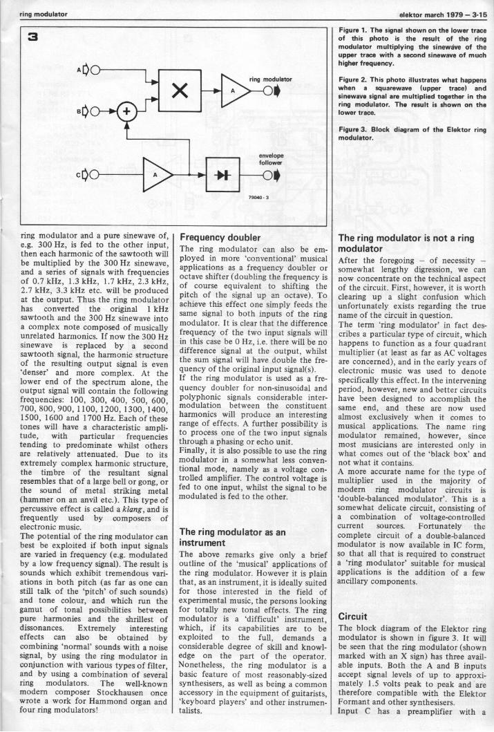
ring modulator elektor march 1979 - 3-15
ring modulator and a pure sinewave of,e.g. 300 Hz, is fed to the other input,then each harmonic of the sawtooth willbe multiplied by the 300 Hz sinewave,and a series of signals with frequenciesof 0.7 kHz, 1.3 kHz, 1.7 kHz, 2.3 kHz,2.7 kHz, 3.3 kHz etc. will be producedat the output. Thus the ring modulatorhas converted the original 1 kHzsawtooth and the 300 Hz sinewave intoa complex note composed of musicallyunrelated harmonics. If now the 300 Hzsinewave is replaced by a secondsawtooth signal, the harmonic structureof the resulting output signal is even`denser' and more complex. At thelower end of the spectrum alone, theoutput signal will contain the followingfrequencies: 100, 300, 400, 500, 600,700, 800, 900, 1100, 1200, 1300, 1400,1500, 1600 and 1700 Hz. Each of thesetones will have a characteristic ampli-tude, with particular frequenciestending to predominate whilst othersare relatively attenuated. Due to itsextremely complex harmonic structure,the timbre of the resultant signalresembles that of a large bell or gong, orthe sound of metal striking metal(hammer on an anvil etc.). This type ofpercussive effect is called a klang , and isfrequently used by composers ofelectronic music.The potential of the ring modulator canbest be exploited if both input signalsare varied in frequency (e.g. modulatedby a low frequency signal). The result issounds which exhibit tremendous vari-ations in both pitch (as far as one canstill talk of the 'pitch' of such sounds)and tone colour, and which run thegamut of tonal possibilities betweenpure harmonies and the shrillest ofdissonances. Extremely interestingeffects can also be obtained bycombining `normal' sounds with a noisesignal, by using the ring modulator inconjunction with various types of filter,and by using a combination of severalring modulators. The well-knownmodern composer Stockhausen oncewrote a work for Hammond organ andfour ring modulators!
Frequency doublerThe ring modulator can also be em-ployed in more 'conventional' musicalapplications as a frequency doubler oroctave shifter (doubling the frequency isof course equivalent to shifting thepitch of the signal up an octave). Toachieve this effect one simply feeds thesame signal to both inputs of the ringmodulator. It is clear that the differencefrequency of the two input signals willin this case be 0 Hz, i.e. there will be nodifference signal at the output, whilstthe sum signal will have double the fre-quency of the original input signal(s).If the ring modulator is used as a fre-quency doubler for non -sinusoidal andpolyphonic signals considerable inter -modulation between the constituentharmonics will produce an interestingrange of effects. A further possibility isto process one of the two input signalsthrough a phasing or echo unit.Finally, it is also possible to use the ringmodulator in a somewhat less conven-tional mode, namely as a voltage con-trolled amplifier. The control voltage isfed to one input, whilst the signal to bemodulated is fed to the other.
The ring modulator as aninstrumentThe above remarks give only a briefoutline of the 'musical' applications ofthe ring modulator. However it is plainthat, as an instrument, it is ideally suitedfor those interested in the field ofexperimental music, the persons lookingfor totally new tonal effects. The ringmodulator is a 'difficult' instrument,which, if its capabilities are to beexploited to the full, demands aconsiderable degree of skill and knowl-edge on the part of the operator.Nonetheless, the ring modulator is abasic feature of most reasonably -sizedsynthesisers, as well as being a commonaccessory in the equipment of guitarists,`keyboard players' and other instrumen-talists.
Figure 1. The signal shown on the lower traceof this photo is the result of the ringmodulator multiplying the sinewave of theupper trace with a second sinewave of muchhigher frequency.
Figure 2. This photo illustrates what happenswhen a squarewave (upper trace) andsinewave signal are multiplied together in thering modulator. The result is shown on thelower trace.
Figure 3. Block diagram of the Elekto ringmodulator.
The ring modulator is not a ringmodulatorAfter the foregoing - of necessity -somewhat lengthy digression, we cannow concentrate on the technical aspectof the circuit. First, however, it is worthclearing up a slight confusion whichunfortunately exists regarding the truename of the circuit in question.The term 'ring modulator' in fact des-cribes a particular type of circuit, whichhappens to function as a four quadrantmultiplier (at least as far as AC voltagesare concerned), and in the early years ofelectronic music was used to denotespecifically this effect. In the interveningperiod, however, new and better circuitshave been designed to accomplish thesame end, and these are now usedalmost exclusively when it comes tomusical applications. The name ringmodulator remained, however, sincemost musicians are interested only inwhat comes out of the 'black box' andnot what it contains.A more accurate name for the type ofmultiplier used in the majority ofmodern ring modulator circuits is`double -balanced modulator'. This is asomewhat delicate circuit, consisting ofa combination of voltage -controlledcurrent sources. Fortunately thecomplete circuit of a double -balancedmodulator is now available in IC form,so that all that is required to constructa 'ring modulator' suitable for musicalapplications is the addition of a fewancillary components.
CircuitThe block diagram of the Elektor ringmodulator is shown in figure 3. It willbe seen that the ring modulator (shownmarked with an X sign) has three avail-able inputs. Both the A and B inputsaccept signal levels of up to approxi-mately 1.5 volts peak to peak and aretherefore compatible with the ElektorFormant and other synthesisers.Input C has a preamplifier with a
3-16 - elektor march 1979 ring modulator
4
0 C10
C 0O-IF470n
P1
A
B
15 V 0
R7
CI 861=1
1000169
EMI
R8 an
R31. 1 R
C2
I
P3
IA5000
2
0 Al
15 V
0
14
R169
120n
C3
E120n
IC1LM 1496N
RI7
12
0 RIZ 0P
2200
15 V C
2
R18
ECM
R19
Al ... A4 = IC2 = TL 084
2
3
R20
Ell
A3
15 V
15V
IC2
921
arta Fring
modulator
O4700
O
AlC4 R24
C55
D37
A2R28 R29
A4
R32
22n13
680k
R23
180n DUS
R26
1131110klog
R22
820k
2x Dl
R30 R25C6 R2711 C7 C8
IMO931
DUS 70n 720n 22n
R33
envelopefollower
ICEEB
79040 4
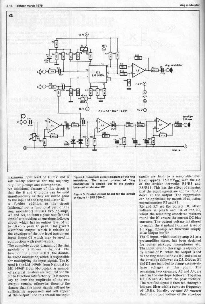
maximum input level of 10 mV and issufficiently sensitive for the majorityof guitar pickups and microphones.An additional feature of this circuit isthat the B and C inputs can be usedsimultaneously as they are mixed priorto the input of the ring modulator IC.A further addition to the circuit(although not a functional part of thering modulator) utilises two op -amps,A2 and A4, to form a peak rectifier andamplifier providing an envelope followercircuit which has an output level of upto 10 volts peak to peak. This gives awaveform output which is relative tothe envelope of the low level instrumentinput (input C) which may be used inconjunction with synthesisers.The complete circuit diagram of the ringmodulator is shown in figure 4. Theheart of the circuit is IC 1, the double -balanced modulator, which is responsiblefor multiplying the input signals. The ICused is the LM 1496N from National (orMC 1496P from Motorola). A numberof external resistors are required for theIC to function satisfactorily. It is necess-ary to limit the amplitude of the twooutput signals, otherwise there is thedanger that the input signals will not besufficiently suppressed and will appearat the output. For this reason the input
Figure 4. Complete circuit diagram of the ringmodulator. The actual process of 'ringmodulation' is carried out in the double -balanced modulator IC1.
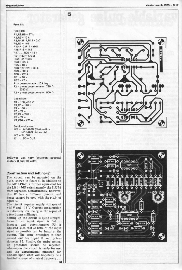
Figure 5. Printed circuit board for the circuitof figure 4 (EPS 79040).
signals are held to a reasonable level(max. approx. 150 mVpp) with the aidof the divider networks R1 /R3 andR8/R11. This has the effect of ensuringthat the input signals are approx. 50 dBdown at the output. The suppressioncan be optimised by means of adjustingpotentiometers P2 and P3.R6 and R7 set the correct DC offsetvoltages at pins 8 and 10 of the IC,whilst the remaining associated resistorsround the IC ensure the correct DC biascurrents. The output voltage is tailoredto match the standard Formant level of1.5 Vpp. Op -amp A3 functions simplyas an output buffer.The C input, which uses op -amp Al as apre -amplifier stage, has been designedfor guitar pickups, microphones etc.The input level to this stage is adjustableby means of P I while the output is fedto the ring modulator via R9 and also tothe envelope follower via C5. Diodes DIand D2 are included to clamp excessivelylarge voltages at this point. Theremaining two op -amps, A2 and A4, areused in the envelope follower. TogetherD3, C6 and A2 form the peak rectifier.The rectified signal is then fed through alowpass filter with a turnover frequencyof 10 Hz. Finally, op -amp A4 ensuresthat the output voltage of the envelope
ring modulator elektor march 1979 - 3-17
Parts list.
Resistors:
R1,R8,R9 - 27 kR2,R5 = 12 kR3,R4,R11,R13 = 2k7R6,R7 = 1k5R10,R12,R14 = 6k8R15,R16 = 1k2R17 ... R20 = 15 kR21,R33 = 470 SiR22,R24 = 5k6R23 = 820 kR25 = 18 kR26,R27,R28 = 68 kR29 = 680 kR30 - 220 kR31 = 10 kR32 = 47 kP1 = potentiometer, 10 k logP2 = preset potentiometer, 220 f2
(250 Si)P3 = preset potentiometer, 500 f2
Capacitors:C1 - 1O0µ(16 VC2,C3 - 120 nC4 = 180 nC5 = 22 nC6,C7 = 220 nC8 = 22 nC9,C10 = 470 n
Semiconductors:ICI = LM 1496N (National) or
MC 1496P (Motorola)IC2 = TL 084D1 . D3 = DUS
follower can vary between approxi-mately 0 and 10 volts.
Construction and setting -upThe circuit can be mounted on thep.c.b. shown in figure 5. In addition tothe MC 1496P, a further equivalent forthe LM 1496N exists, namely the S 5596from Signetics. Unfortunately, however,this IC has a different pin -out, andhence cannot be used with the p.c.b. offigure 5.The circuit requires supply voltages of4-15 V and -15 V. Current consumptionis extremely low, being in the region ofa few dozen milliamps.Setting up the circuit is quite straight-forward: an input signal is fed toinput A and potentiometer P3 isadjusted such that as little of the inputsignal as possible can be heard at theoutput. The same procedure is thencarried out for input B and poten-tiometer P2. Finally, the entire setting -up procedure should be repeated,whereupon the circuit is ready for use,and the experimental musician canembark upon what will hopefully be afruitful 'voyage' of musical discovery . . .
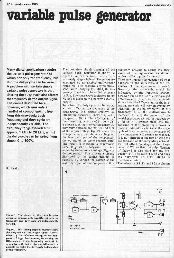
3-18 - elektor march 1979 variable pulse generator
variable pulse generator
Many digital applications requirethe use of a pulse generator ofwhich not only the frequency, butalso the duty -cycle can be varied.A problem with certain simplevariable pulse generators is thataltering the duty -cycle also affectsthe frequency of the output signal.The circuit described here,however, which uses only ahandful of components, is freefrom this drawback; bothfrequency and duty -cycle areindependently variable. Thefrequency range extends fromapprox. 1 kHz to 20 kHz, whilstthe duty -cycle can be varied fromalmost 0 to 100%.
K. Kraft
Figure 1. The circuit of the variable pulsegenerator employs only two ICs, yet both thefrequency and duty -cycle are independentlyvariable.
Figure 2. This timing diagram illustrates howthe duty -cycle of the output signal is deter-mined by the reference voltage of the com-parator (Uref). Furthermore, by varying theRC -constant of the integrating network insympathy with that of the multivibrator it is
possible to make the duty -cycle independentof the frequency.
The complete circuit diagram of thevariable pulse generator is shown infigure 1. As can be seen, the circuit isextremely simple indeed. The pulses aregenerated by an astable multivibratorround Ni. This provides a symmetricalsquarewave (duty -cycle = 50%), the fre-quency of which can be varied by meansof P I a. The squarewave is cleaned up byN2 and is available via an extra externaloutput.To allow the duty -cycle to be variedwithout affecting the frequency of thesquarewave, the circuit employs anintegrating network (Plb/R2/C2) and acomparator (IC I). The RC -constant ofthe integrating network (C2 = 1/6 Cl)is chosen such that the voltage across C2may vary between approx. 20 and 80%of the supply voltage, Ub. Whenever thisvoltage exceeds the reference voltage onthe inverting input of the comparator,the output of the latter changes state.The result is therefore a squarewavesignal (Ux) whose duty -cycle is deter-mined by the reference voltage (Uref) ofthe comparator. This process is clearlyillustrated in the timing diagram offigure 2. By varying the voltage at theinverting input of the comparator it is
therefore possible to adjust the duty -cycle of the squarewave as desiredwithout affecting the frequency.There now remains the question of whathappens to the duty -cycle if the fre-quency of the squarewave is varied.Normally the duty -cycle would heinfluenced by the frequency change,however due to the use of a twin -gangedpotentiometer (PI a/Plb), in the circuitshown here, the RC -constant of the inte-grating network will vary in sympathywith that of the multivibrator. If thefrequency, f, of the multivibrator isincreased to xf, the period of theresulting squarewave will he reduced bya factor x. However since the RC -constant of the integrating network islikewise reduced by a factor x, the duty -cycle of the squarewave at the output ofthe comparator will remain unchanged.It is not difficult to see that altering theRC -constant of the integrating networkwill not affect the shape of the chargecurve of C2, so that the pulse diagramof figure 2 is also valid for any fre-quency xf. The ratio T1 /T2 and thusthe duty -cycle (= TI /T2 x 100%) istherefore constant.The values of R3, R4 and P2 are chosen
P19In
ME ELMOk
NI
D. ID.CIMEI
T5On
ICI. LOA 31IN
1C2k NI ---N4.4093
MHO
1083311
00
5 10y
0=f
84
CO
Tan
ICI
95
79051 I
ED 00
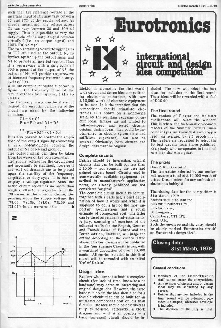
variable pulse generator eurotronics elektor march 1979 - 3-19
such that the reference voltage at theinverting input of ICI may vary between13 and 87% of the supply voltage. Asalready mentioned, the voltage acrossC2 can vary between 20 and 80% ofsupply. Thus it is possible to vary theduty -cycle of the output signal betweenvirtually 0 (i.e. no output signal) and100% (DC voltage).The two remaining Schmitt -trigger gatesof 1C2 are used at the output, N3 tofurther square up the output signal andN4 to provide an inverted version. Thusif a squarewave with a duty -cycle of30% is present at the output of N3, theoutput of N4 will provide a squarewaveof identical frequency but with a duty -
cycle of 70%.With the component values as shown infigure 1, the frequency range of thecircuit extends from approx. 1 kHz to20 kHz.The frequency range can be altered ifdesired; the essential parameters of thecircuit are given by the followingequations:
C I = 6 x C2Pia= Plb and R1 = R2
1f-(Pla+ R1) CI 0.4It is also possible to control the ampli-tude of the output signal by connectinga 22 k potentiometer between theoutput of N3 or N4 and ground.The output signal can then be takenfrom the wiper of the potentiometer.The supply voltage for the circuit neednot necessarily be stabilised, however ifany sort of demands are to be placedupon the stability of the frequency,amplitude or duty -cycle, it is best toemploy a voltage regulator. Since theentire circuit consumes no more thanroughly 20 mA, a regulator from the78L -series is the obvious choice. De-pending upon the supply voltage, the78L05, 78L06, 78L08, 78L09 and78L010 should prove suitable.
Eurotronics
*IIN*N er ationalt and
* comPetiElektor is promoting the first world-wide circuit and design idea competitionfor electronics enthusiasts, with over£ 10,000 worth of electronic equipmentto be won. It is the intention that thiscompetition should stimulate elec-tronics as a hobby on a world-widescale, by the resulting exchange of cir-cuit ideas. Entries are not limited tofully -developed and tested circuits:original design ideas, that could be im-plemented in circuits (given time andsufficient experience), can also beentered. Obviously, both circuits anddesign ideas must be original.
Complete circuitsEntries should be interesting, originalcircuits that can be built for less than£ 20.00 - not counting the case andprinted circuit board. Circuits used incommercially available equipment, de-scribed in manufacturer's applicationnotes, or already published are notconsidered `original'.The complete circuit should be sent in,together with a parts list, a brief expla-nation of how it works and what it issupposed to do, a list of the most im-portant specifications and a roughestimate of component cost. The lattercan be based on retailer's advertisements.A jury, consisting of members of theeditorial staffs for the English, Germanand French issues of Elektor and theDutch edition, Elektuur, will judge theentries according to the criteria listedabove. The best designs will be publishedin the four Summer Circuits issues, witha combined circulation of over 250,000copies. All entries included in this finalround will be rewarded with an initial`fee' of £ 60.00.
Design ideasReaders who cannot submit a completecircuit (for lack of time, know-how orhardware) may enter an interesting andoriginal design idea. However, the samebasic rule holds: the idea should be for afeasible circuit that can be built for anestimated component cost of less than£ 20.00. The idea should be described asfully as possible. Perferably, a blockdiagram and - if at all possible - abasic (untested) circuit should be in -
eluded. The jury will select the bestideas for inclusion in the final round.These ideas will be rewarded with a 'fee'of £ 20.00.
The final roundThe readers of Elektor and its sisterpublications will select the winners!This is where the half -a -million -or -morereaders of the Summer Circuits issuescome in (yes, we know that each copy isread, on average, by 2.6 people ... ).The readers are requested to select the10 best circuits from those published.Everybody who co-operates in this finalvote may also win a prize.
The prizesOver £ 10,000 worth!The ten entries selected by our readerswill receive a total of £ 10,000 worth ofprizes. Dream prizes for any enthusiasticelectronics hobbyist!
The closing date for the competition is31st March, 1979.Entries should be sent to:Elektor Publishers Ltd.,Elektor house,10 Longport,Canterbury, CT1 1PE,Kent, U.K.Both the envelope and the entry shouldbe clearly marked 'Eurotronics circuit'or 'Eurotronics design idea'.
Closing date:31st March, 1979.
General conditions
Members of the Elektor/Elektuurstaff cannot enter the competition.
Any number of circuits and/or designideas may be submitted by anyperson.
Entries that are not included in thefinal round will be returned, pro-vided a stamped, addressed envelopeis included.
The decision of the jury is final.
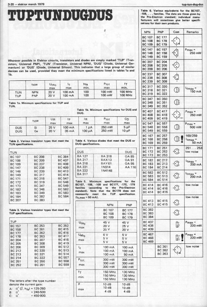
3-20 - elektor march 1979 tup-tun-dug-dus
TUPTUNDUGDUS
Wherever possible in Elektor circuits, transistors and diodes are simply marked 'TUP' (Tran-sistors, Universal PNP), "TUN' (Transistor, Universe) NPN), 'DUG' (Diode, Universal Ger-manium) or 'DUS' (Diode, Universal Silicon). This indicates that a large group of similardevices can be used, provided they meet the minimum specifications listed in tables la andlb.
T
type Uceomax
1
Ic hfemax min.
I
Ptotmax
fTmin.
TUNTUP
NPNPNP
20 V20 V
100 mA100 mA
100100
100 mW100 mW
100 MHz100 MHz
Table la. Minimum specifications for TUP andTUN.
Table lb. Minimum specifications for DUS andDUG.
type UR I F
max maxI R
maxPtotmax
I CDmax
DUSDUG
Si
Ge
25 V20V
100 mA35 mA
1 µA100µA
i
250 mW250 mW
1
'
5 pF10 pF
Table 2. Various transistor types that meet theTUN specifications.
TUNBC 107BC 108BC 109BC 147BC 148BC 149BC 171BC 172BC 173BC 182BC 183BC 184BC 207
BC 208BC 209BC 237BC 238BC 239BC 317BC 318BC 319BC 347BC 348BC 349BC 382BC 383
BC 384BC 407BC 408BC 409BC 413BC 414BC 547BC 548BC 549BC 582BC 583BC 584
Table 3. Various transistor types that meet theTUP specifications.
TUP
BC 157 BC 253 BC 352BC 158 BC 261 BC 415BC 177 BC 262 BC 416BC 178 BC 263 BC 417BC 204 BC 307 BC 418BC 205 BC 308 BC 419BC 206 BC 309 BC 512BC 212 BC 320 BC 513BC 213 BC 321 BC 514BC 214 BC 322 BC 557BC 251 BC 350 BC 558BC 252 BC 351 BC 559
The letters after the type numberdenote the current gain:A a' (0, hfe( = 125-260B: U' - 240-500C - 450-900.
Table 4. Various diodes that meet the DUS orDUG specifications.
DUS DUGBA 127BA 217BA 218BA 221BA 222BA 317
BA 318BAX 13BAY611N9141N4148
OA 85OA 91OA 95AA 116
Table 5. Minimum specifications for theBC107, -108, -109 and BC177, 17C, -179families (according to the Pro -Electronstandard). Note that the BC179 does notnecessarily meet the TUP specification(Ic,max = 50 mA).
NPN PNP
BC 107BC 108BC 109
BC 177BC 178BC 179
Uceo
max
45 V20 V20V
45 V25 V20V
Uebo
max
6 V5 V5V
5 V5 V5V
Ic
max
100 mA100 mA100 mA
100 mA100 mA50 mA
Ptot.
max
300 mW300 mW300 mW
300 mW300 mW300 mW
fTmin.
150 MHz150 MHz150 MHz
130 MHz130 MHz130 MHz
F
max
10 dB10 dB4 dB
10 dB10 dB4 dB
Table 6. Various equivalents for the BC107,-108, . . families. The data are those given bythe Pro -Electron standard; individual manu-facturers will sometimes give better specifi-cations for their own products.
NPN PNP Case Remarks
BC 107BC 108BC 109
BC 177BC 178BC179
BQ
BC 147BC 148BC 149
BC 157BC 158BC 159
". Pmax =250 mW
BC 207BC 208BC 209
BC 204BC 205BC 206
e0
BC 237BC 238BC 239
BC 307BC 308BC 309
N'..tj
BC 317BC 318BC 319
BC 320BC 321BC 322
rr,\L' '
Icmax =150 mA
BC 347BC 348BC 349
BC 350BC 351BC 352
. .
.
BC 407BC 408BC 409
BC 417BC 418BC 419
-Pmax =
250 mW
BC 547BC 548BC 549
BC 557BC 558BC 559
,, 500E Pmax =mW
BC 167BC 168BC 169
BC 257BC 258BC 259
. tIcmax169/259
=50 mA
BC 171BC 172BC 173
BC 251BC 252BC 253
.
251 . .. 253low noise
BC 182BC 183BC 184
BC 212BC 213BC 214
Icmax -200 mA
BC 582BC 583BC 584
BC 512BC 513BC 514
E.i axcm2O0 mA
BC 414BC 414BC 414
BC 416BC 416BC 416
C.low noise
BC 413BC 413
BC 415BC 415
Agi
4151'
low noise
BC 382BC 383BC 384
zBC 437BC 438BC 439
ili Pmax220 mW
BC 467BC 468BC 469
OF :Pmax =
220 mW
BC 261BC 262BC 263
'low noise
sinewave generator elektor march 1979 - 3-21
sinewave generator
In last month's issue of Elektor wepublished a design for a spotsinewave generator which offeredtruly 'top-notch' specifications.For the purposes of manyamateurs, however, the accuracyprovided by such a circuit (e.g.harmonic distortion of less than0.0025%) is an expensive luxury.The circuit described hererepresents the other side of thecoin - a simple cost-effectivesinewave generator whosefrequency can be continuouslyvaried over virtually the entireaudio spectrum, while being easyto construct and requiring nocalibration. Just for good measurethe circuit also offers the choiceof a squarewave output.
Figure 1. Block diagram of the sinewavegenerator.
The idea of incorporating a limiter inthe feedback loop of an oscillatorcircuit as a means of stabilising theamplitude of the output signal wasoriginally employed in the spot sinewavegenerator published in last month's issueof Elektor. That circuit was designed forextremely low harmonic distortion andhigh amplitude stability. The circuitdescribed here, although employing asimilar principle to its 'big brother' oflast month, is intended to meet a differ-ent set of criteria. It was felt that manyamateurs would appreciate a simple low-cost sinewave generator with continu-ously variable frequency which wouldrequire no complicated calibrationprocedure.
Block diagramThe block diagram of the simplesinewave generator is shown in figure 1.A selective filter is followed by a limiter
circuit which clamps the signal level to+ and -Ub. The output of the limiter isfed back to the input of the selectivefilter, thereby providing the conditionsfor oscillation. The circuit will onlycontinue to oscillate if the loop gain ofthe system is greater than unity. Toensure that this requirement is alwayssatisfied an amplifier is included in thefeedback loop. The circuit is forced tooscillate at the centre frequency of thefilter, since only at that frequency willthe in- and output signals of the filter bein phase.The reason why the amplitude of theoutput voltage of such an oscillatorremains constant was described in detailin the above -mentioned article on thespot sinewave generator, to whichreaders are here referred. A continu-ously variable oscillator frequency isobtained by making the centre fre-quency of the selective filter tunable.The Q of the filter will inevitably varywith the centre frequency, therebyaffecting the suppression of higher
3-22 - elektor march 1979 sinewave generator
2
12
13
R2
Al
El]
R314 EMI
R4
D6 R9Cl
720P
1:15
2 x 5V6400 mW
EEL/3
R7
R22
Re
A2
R23
P1a10klog
2
* L-1,15 R6 R20
TU
3
C6
In
A3R27
P1b10klog
R21 *
U
C7
P247klog
in
A422. +
0
O
0ICI
0
Al ... A4 = TL 084 = IC1D1 ... D4 = 4x 1N4001
S1
F1
400mA
DI
Tr 1
I8V
D2
0
3
DO
R11
C2O4701'
40V
R12
0
C3
100n
LEM
R10
C5
R19
22PR18 2x
BC5478
0R24
0
e13
IT`
R14
T1R13
mcsi be'vA
BC557B C4
TOOn
R15
T4
dr4ILL
R16
BC547B
R17
R25
9
BC557B
16
esILL
79019 2
BC5478
48 oFFE--.1
*see text
10416V
O
harmonics in the output signal, andhence the purity of the sinewave.However, some degradation in waveformpurity is the inevitable consequence ofhaving a continuously variable outputfrequency, and as has already beenemphasised, the harmonic distortion ofthe circuit was deemed to be of second-ary importance - within certain limitsof course - in a project designed forminimum cost and maximum simplicity.The output of the limiter is a clippedsinewave, i.e. a trapezoidal waveform,which is then shaped by a Schmitttrigger providing a squarewave outputsignal with a duty -cycle of 50%. Theoutput of the Schmitt trigger is bufferedand is available both with and without aDC offset.
CircuitThe complete circuit diagram of thesinewave generator is shown in figure 2.
The selective filter formed by op -ampsA2 . . . A4 is of the 'variable state' type,and comprises two integrators and asumming amplifier. The centre fre-quency of the filter can be varied bymeans of P1. It is apparent that howwell the two gangs of this potentiometerare matched will determine the ampli-tude stability of the output signal forchanges in frequency.The output of A3 (which is also fedback to A 1) supplies the sine waveoutput of the generator. A 1 is configuredas an amplifier with a gain of ten and itsoutput is clamped to approximately12 volts peak to peak by means of zenerdiodes D5 and D6, before being fedback to the input of the selective filter.The clipped sinewave is also fed (via R9)to the Schmitt trigger formed by transis-tors T2, T3 and T4, with the resultingsquarewave being buffered by transistorsT5 and T6. The circuit operates off a24 V supply. A virtual earth point iscreated via R11, R12, R13 and T 1 , so
that a roughly symmetrical supply of± 12 V is obtained.
ConstructionThe component layout and trackpattern of the p.c.b. for the sinewavegenerator is shown in figure 3. One caneither provide the case with threeseparate output sockets, or else use asingle socket with a three-way waveformselector switch.The circuit requires no calibration. Theonly preliminary measure which, in viewof component tolerances, may provenecessary is to experiment slightly withthe value of R20 and R21. The fre-quency range of the sinewave generatoris approx. 20 Hz to 25 kHz. The ampli-tude of the sinewave output is constantover the range 150 Hz to 6 kIIz. Abovethis point there is a very slight rise inamplitude, and below 150 Hz the ampli-tude will tend to fall slightly. Harmonic
sinewave generator elektor march 1979 - 3-23
Figure 2. Complete circuit diagram. The am-plitude of the sinewave output signal can bevaried by means of P2.
Figure 3. Track pattern and componentlayout of the p.c.b. for the sinewave generator(EPS 79019). Only the transformer andpotentiometers are mounted off -board.
Parts list
Resistors:
R1,R17 = 100kR2= 10kR3,R10,R19 = 2k2R4,R7 = 330 kR5,R6,R8,R22 = 27 kR9 = 22 kR11,R12 = 6k8R13 = 1 kR14 = 120 kR15 = 47 kR16,R26 = 1k5R18 = 82 kR20,R21 = 39 D (see text)R23,R27 = 5k6R24 = 2k7R25 = 8k2P1a/b = stereo potentiometer,
10 k log.P2 = potentiometer, 47 k log.
Capacitors:
C1 = 220 pC2 = 470 µ/40 VC3,C4 = 100 nC5 = 22 pC6,C7 = 1 n
C8 = 10 p./16 V
Semiconductors:T1,T5 = BC 5576T2,T3,T4,T6 = BC 5476101 = TL 084D1 ... D4 = 1N400105,D6 = 5V6/400 mW
Miscellaneous:
S1 = mains on/off switch,400 mA
F1 = fuse, 400 mAtransformer, 18 V/50 mA
distortion is less than 1% over the entirefrequency range. The amplitude of thesquarcwave output is virtually constantover the entire range (8 Vpp).Current consumption is roughly 12 mA.
3-24 - elektor march 1979 applikator
Universal CounterMicroprocessors and digital memories are notthe only product areas to be influenced bythe ever increasing chip densities achieved inLSI (Large Scale Integration) devices. Othermore 'traditional' logic functions, which oncewere implemented using a mountain of dis-crete TTL- or CMOS ICs can now be realisedwith a single LSI chip.This point was well illustrated by the designfor the Elektor '1/4 GHz Counter' publishedin June 1978. The heart of the above circuitwas a six -decade counter/display driver IC,the MK 50398N from Mostek. This one IC didthe job which previously would have requireda boxful of 7490's, 7475's etc.As 'intelligent' as it was, however, theMK 50398N was by no means the last wordon this subject, and sure enough, a new familyof LSI counter/timer ICs has recently beenannounced, whose performance represents anadvance on anything seen so far.The device in question is the ICM 7216A/B/C/D from Intersil. As the type numbersuggests, there are four different versions ofthe chip; the ICM 7216A and 13 are fullyintegrated universal counters/display driversfor common -anode and common -cathode dis-plays respectively (see table 11, whilst theICM 7216C and D are frequency counter onlyversions of the above.The chips combine a high frequency crystaloscillator, a decade timebase counter, an eightdecade data counter plus latches, and associ-ated elements for decoding, multiplexing and
driving 8 large LED displays. Gate times of.01, 0.1, 1 and 10 seconds in the frequencycounter mode allow input frequencies of upto 10 MHz. In the case of the 7216A and Bthe maximum input frequency in other modesis 2 MHz, whilst times can be measured over1, 10, 100, and 1000 cycles to give periodmeasurement from 0.5 µs to 10 seconds.Additional features include: decimal pointand leading zero blanking automatically con-trolled by the chip, hold and reset inputs, lowpower/display off mode, and internal test anddisplay test functions. A single nominal 5 Vsupply is the sole power requirement.
Universal Counter
Of the four available versions of the chip, theICM 7216A and B are the most interesting inview of the truly impressive range of differentfunctions which they offer.In addition to frequency counting, the devicescan operate as a period counter, frequencyratio counter, time interval counter, and unitcounter. The internal organisation of the chipis illustrated by the block diagram of figure 1.The input signal is fed to input A, whereuponcontrol logic determines whether it is fed tothe clock input of the main counter, orwhether (when measuring period, for instance)it is used to gate the internal clock signal ofthe IC to the main counter. The number ofclock pulses counted by the latter is then anindex for the length of the period.When a 'store' pulse is received from the con-trol logic, the contents of the main 108 coun-
ter are transferred to the data latches, The8 digit count data is converted into 7 -segmentcode and multiplexed to the segment outputs.As already mentioned, the counter canmeasure more than simply frequency andperiod. When operated in the 'unit counter'mode, it counts the total number of pulses inthe input signal (instead of the number ofpulses per second). The chip will also measurethe frequency ratio between two input signals, a facility which in certain situations canoffer advantages over simple measurement offrequency. If, for example, an extremelystable reference frequency is available, inprinciple it is possible to measure an unknowninput frequency with greater accuracy usingthis method. Furthermore, there are instanceswhere the ratio of two frequencies is moreimportant than their exact value, or where thefrequencies vary but the ratio remains con-stant (e.g. in certain music applications). Whenfunctioning in the frequency ratio mode oneinput signal is fed to input A, the other toinput B. To ensure good accuracy, the fre-quency of the signal fed to input A should begreater than that at input B. If the frequencyratio is greater than 105, all 8 digits of thedisplay can be used.
The fifth type of measurement of which thechip is capable is time interval. The chipcounts the number of microseconds whichelapse between a 1-0 transition occurring atinput A and a 1-0 transition at the B input.To complete the measurement cycle input Amust again go negative after B goes negative
EATOSC 0
INwTOSC
INur
OSCOUTPUT
OSC,ELECT
NR mos1000 z
RANGE SELECTIDOIC
DECOOER =O.
0
CON,RoLLOGIC
ONE/TOLLOGIC
STORE
B DIGITOunv is
9,
RANGE RANGECONTROL :PUT
LOGIC
CL
10X COUNTER
GLEE FLOM
4 /P /
0uZuT DATA LATCHES STORE
EN
CONTR.ocic
Tr
JPLOGIC
LOGIC
7CONTR..
LOGIC
SEGMENT),:VE.
790 4 4 1
CONTROLOT
I 11107.4597'*0 Ou TOUTS
Under the heading Applikator, recently introduced components and novel applications are described. The data and circuits given are based oninformation received from the manufacturer and/or distributors concerned. Normally, they will not have been checked, built or tested by Elektor.
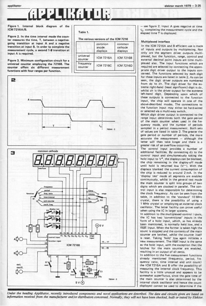
applikator elektor march 1979 - 3-25
Figure 1. Internal block diagram of theICM 7216A/B.
Figure 2. In the time interval mode the coun-ter measures the time, T, between a negative -going transition at input A and a negativetransition at input B. In order to complete themeasurement cycle, a second 1-0 transition atinput A is required.
Figure 3. Minimum configuration circuit for auniversal counter employing the 7216B. Thecounter offers six different measurementfunctions with four ranges per function.
Table 1.
The various versions of the ICM 7216
commonanodedisplays
commoncathodedisplays
universalcounter ICM 7216A ICM 72166
frequencycounter ICM 7216C ICM 7216D
common cathodennnonnn1713.0. LI. El. LI. a LI. LI.
function
141
A00-
overflow
frequenc
pe od
rep ratio
0.. time interval
unit counter
frorc ill. eq
display test
displey blank4 0118:3132
ext. oscillator
10ms
12 11 10 7 5 6 4
100ms
14
renia
05 V
18
3
28
2
B00-
ext.oscill.
00
24
d7 do d5 de 43 d2 di d0 rangecoot of input input
function input
ICM 7216615 17
Sireset
27
R4
25
R5
26
19 23
X-tal
Cl 01-*OM 10 MHz g
hold MEP39P 39p
5 V C)79044 3
- see figure 2. Input A goes negative at timetc, completing the measurement cycle and theelapsed time T is displayed.
Multiplexed interfaceIn the ICM 7216A and B efficient use is madeof inputs and outputs by multiplexing. Notonly are the segment driver outputs multi-plexed, but the function, range, control andexternal decimal point inputs are time multi-plexed also. The input functions which arerequired are selected by connecting the appro-priate digit driver output to the inputs con-cerned. The functions selected by each digitfor these inputs are listed in table 2. As can beseen, the digit driver outputs are numberedfrom do to d7. The digit driver for the ex-treme right-hand (least significant) digit is do,whilst cl7 is the driver output for the extremeleft-hand digit. Depending upon which ofthese outputs is connected to the functioninput, the chip will operate in one of theabove -described modes. The connections tothe function input may either be hard -wiredor selected via a multi -way switch.Which digit driver output is connected to therange input determines both the gate periodof the main counter when used in the fre-quency mode, and the number of periodssampled in a period measurement. Both setsof values are listed in table 2. The greater thegate period or number of periods, the moreaccurate the measurement - although thelatter will then take longer and there is a
greater risk of an overflow occurring.The control input provides a number ofadditional facilities. By connecting d3 to thecontrol input and simultaneously taking thehold input to V+, the displays can be blanked,the chip remaining in the display -off modeuntil hold is returned low (V--). With thedisplays blanked the current consumption ofthe chip is reduced to around 2 mA. In the'display test' mode all segments are enabledcontinuously, whilst in the general test modethe main counter is split into groups of twodigits which are clocked in parallel. The con-trol input is also responsible for determiningthe clock frequency. As can be seen from thetable, in addition to the 'standard' 10 MHzcrystal, there is the possibility of using a
1 MHz crystal or employing an external clockoscillator. The latter facility can prove usefulwhen using the IC in larger systems.In addition to the multiplexed control i,-.puts,the IC has two 'conventional' inputs in theform of a hold input, which, as has alreadybeen mentioned, is normally held low, and areset input. When the former is taken high thecount is stopped and the contents of the maincounter are latched, whilst the counter itselfis reset. Taking 'hold' low again initiates anew measurement. The reset input is the sameas the hold input, with the exception that thelatches for the main counter are enabled,resulting in an output of all zeros.In addition to the five measurement functionsalready mentioned (frequency, period, fre-quency ratio, time interval and unit count)the ICM 7216A and B offer the possibility ofmeasuring the internal clock frequency. Thisfacility is a little unusual and appears to besomewhat superfluous, since the gate time ofthe main counter is also determined by theinternal clock oscillator and hence the countdisplayed cannot be used to determine if the
Under the heading Applikator, recently introduced components and novel applications are described. The data and circuits given are based oninformation received from the manufacturer and/or distributors concerned. Normally, they will not have been checked, built or tested by Elektor.
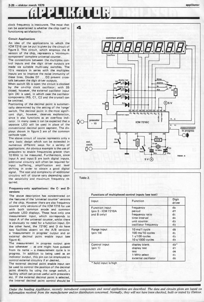
3-26 - elektor march 1979 applikatorPL CIclock frequency is inaccurate. The most thatcan be ascertained is whether the chip itself isfunctioning satisfactorily.
Circuit ApplicationsAn idea of the applications to which theICM 7216 can be put is given by the circuit offigure 3. This circuit, which employs the Bversion of the chip, represents a 'minimum -component' complete universal counter.The connections between the multiplex con-trol inputs and the digit driver outputs aremade via suitable multi -way switches. The10 k resistors in series with the multiplexinputs are to improve the noise immunity ofthese lines. Diodes D1 ... D3 prevent cross-talk between the digit driver outputs.When switch S5 is open the circuit is clockedby the on -chip clock oscillator; with S5closed, however, the external oscillator input(pin 24) is used, in which case the oscillatorcomponents (R5, C1, C2 and the crystal) canbe omitted.Positioning of the decimal point is automati-cally determined by the setting of the 'range'switch. The decimal point in the most signifi-cant digit, however, deserves explanation,since it also functions as an overflow indi-cator. In many cases it can be expected that aseparate LED will be used in place of theconventional decimal point segment. The dis-plays shown in figure 3 are of the commoncathode type.The above circuit of course represents only avery basic design which can be extended innumerous different ways for a variety ofapplications. An obvious example is the use ofprescalers to enable frequencies greater than10 MHz to be measured. Furthermore, sinceinput A and input B are both digital inputs,additional circuitry will often be required forinput buffering, amplification and levelshifting in order to obtain a good digitalsignal. The cost and complexity of additionalcircuitry will of course vary depending uponthe sensitivity and maximum frequency re-quired.
Frequency -only applications: the C- and D -
versions
The above description has concentrated onthe features of the 'universal counter' versionsof the chip. However there are also frequencycounter only versions of the ICM 7216 for usewith both common anode and commoncathode LED displays. These have only onemeasurement input, which corresponds toinput A of the universal counter, whilst thereis obviously no need for a function input. Onthe other hand, the 7216C and D do havetwo facilities absent on the A/B versions:a 'measurement in progress' output and anexternal decimal point enable input (seefigure 4(.The measurement in progress output goeslow whenever - as one might have guessedfrom its name - a measurement cycle is inprogress. In addition to being used as anindicator output, this pin can be employed tocontrol external circuitry if se desired.The external decimal point enable input canbe used to control the position of the decimalpoint directly by using the range switch, a
facility which can prove useful with prescalersetc. If the external decimal point is selected,the internal decimal point control should be
4common anode
11 I 0 lln 1'7 11 11tail. O. L I. a o. a o.
0- prescaler- 10
ext.oscill.
Eo
overflow
display test
display blink400002
est. oscillator
15 6 7 19 20 21
toms
100in
1s
22
10 A SIAl
23 13741 18
5V
J control Inputd d6 us ,14 43d2 di do Zs i
28ICM 7216C
4
3 6
8 11
2
SS
reset3
7i 25
0
26
R4
X-tal
C I 41 1.11 C 2
holdMN 10 MHz gmin
39p 39p
5V ci
measurementin progress
79044 -4
Table 2.
Functions of multiplexed control inputs (see text)
Input Function Digitdriver
Function input(pin 3 - ICM 7216Aand B only)
frequencyperiodfrequency ratiotime intervalunit counteroscillator frequency
dod7did4d3d2
Range input(pin 141
10 ms/1 cycle100 ms/10 cycles1 s/100 cycles10 s/1000 cycles
dodid2d3
Control input(pin 11
display blankdisplay testtest1 MHz selectexternal oscillator
d3*d7d4dido
hold input is high
Under the heading Applikator, recently introduced components and novel applications are described. The data and circuits given are based oninformation received from the manufacturer and/or distributors concerned. Normally, they will not have been checked, built or tested by Elektor.
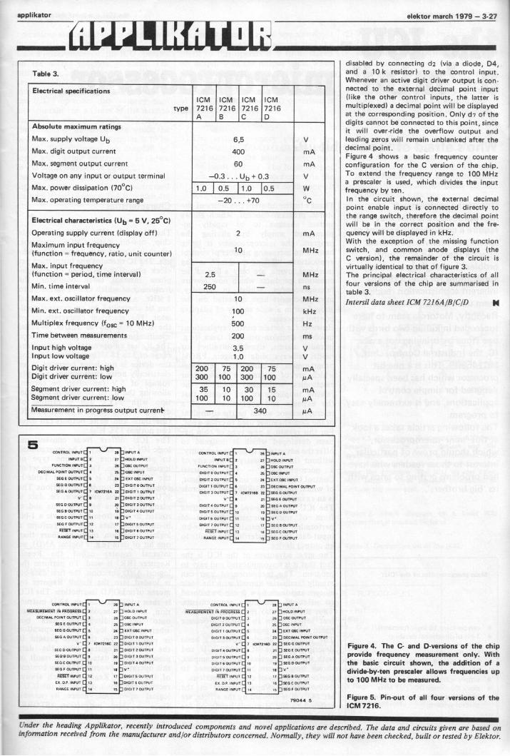
applikator elektor march 1979 - 3-27
PPLIKA DRTable 3.
Electrical specificationsICM ICM ICM ICM
type 7216 7216 7216 7216A BC D
Absolute maximum ratings
Max. supply voltage Ub 6,5 V
Max. digit output current 400 mA
Max. segment output current 60 mA
Voltage on any input or output terminal -0.3 ... Ub + 0.3 V
Max. power dissipation (70°C) 1.0 0.5 1.0 0.5 W
Max. operating temperature range -20 . +70 'C
Electrical characteristics (Ub = 5 V, 25°C)
Operating supply current (display off) 2 mA
Maximum input frequency(function = frequency, ratio, unit counter) 10 MHz
Max. input frequency(function = period, time interval) 2.5 - MHz
Min. time interval 250 ns
Max. ext. oscillator frequency 10 MHz
Min. ext. oscillator frequency 100 kHz
Multiplex frequency (low = 10 MHz) 500 Hz
Time between measurements 200 ms
Input high voltage 3.5 VInput low voltage 1.0 V
Digit driver current: high 200 75 200 75 mADigit driver current: low 300 100 300 100 µA
Segment driver current: high 35 10 30 15 mASegment driver current: low 100 10 100 10 µA
Measurement in progress output current- - 340 µA
5CONTROL INK, C 31mpul A CONTROL INPUT C 3 MINT 7-/-7.
INPUT SC 2 2T 3NOTD INPUT INPUT RC 2 27 >1010 ImpuTFUNCTION INPUT 3 26 3,764 OUTPUT FUNCTION INPUT C 3 26 DOSC CAITPUT
DECIMAL POINT OUTPUT[ 4 26 DOSC INPUT DIGIT 0 OUTPUT C 4 25 3OSC INPUTSEG E OUTPUT C 5 243Exf OSCINuT DIGIT 2 OUTPUT C 2+1 3E XT 051C INPUTSEGO OUTPUT[ 23 ]DIGIT 0 OvITul DIGIT I OUTPUT C 6 23 3 DECIMAL POINT OUTPUTSEG A OUTPUT C 7 10.7216A 22 3 DIGIT 1 OUTPUT DIGIT 3 OUTPUT C ICM72161 22 3 SEG GOLJTM22
v C zi 0101, 2 OUTPuT V' C 213 SEG E OUTPUTSEG 0 OUTPUT C 9 20 3 DIGIT 3 OUTPUT DIGIT 4 OUTPul C 9 20 3 SEG A OuTpuTSEG B OUTPUT C TO 19 3 DIGIT 4 OUTPUT DIGIT OUTPUT C 10 19 35E6000,1,gUGC OUTPUT C +8 Dy DIGIT 6 OUTPUT C IT 16 3SEG F 041,072 C 12 1T ]DIGIT 5 OUTPUT DIGIT T OUTPUT C 12 17 3 SEG OuTNTWET INPUT C 13 It 3 DIGIT 6 OuTPuT RRESETINN! C 13 16 3 SEG C OUTPUTRANGE (NUT[ 14 15 30101T )OUTPUT RANGE 1NPur C 14 IS 3 SEGF OUTPUT
CONTROL INPUT C 3 INPUT A CONTROL INPUT [T"3 IMP," AMEASUREMENT PROGRESS C 2 27 3001.0 INPUT MEASUREMENT IN PROGRESS C 2 27 30050151Pu,
DECIMAL POINT OUTPUT L 3 26 '30SC Ouipul DIGIT 0 3 26 3 OSC OUTPUT
SEG E OUTPUT C 25 E DSC INPUT 2 Wu, T C 4 25 30SC !NoviSEG G OUTPUT C 2435 ExT OSC INPur 01013 1 OUTPUT C 5 24 3 EXT 06C INPUT
SEG A OUTPUT C 6 233 DIGIT 0 OUTPUT DIGIT 3 OUTPUT C 6 23 3 DECIMAL POINT OUTPUT
v" C 1 icM72111C 22 2 DIGIT 1 OUTPUT C 7 ic74221615 22 3 SEG G OUTPUT
SEG DOUTPuT C S 21 3 DIGIT 2 OuTPuT DIGIT OUTPUT C II 21 3 SEC E OUTPuT
SEG B OUTPUT C 9 203 DIGIT 3 OUTPUT DIGIT 5 OuTPuT 9 20 3 SEG A OUTPuT
ST G C OUTPUT C 10 19 D DIGtT ouTpuT DIGIT IS OUTPUT 10 I 0 OUTPUT
SEG F OUTPUT la 3s, DIGIT 7 OUTPUT C IT IS
,S.EG
RIFT inanfr C 12 17 D DIGIT 5 OUTPuT RESET INPUT C 12 I 7 3 SEG IOUTPuTEX 0.P INPUT C 13 Is 30101T 6 OuTPLa Ex OP.INPuT C 13 15 ]SEG C OUTPUTRANGE INPUT C 15 3 DIGIT 7 OUTPUT RANGE INPUT C It A 3 SEG f OUTPUT
79044 5
disabled by connecting d2 (via a diode, D4,and a 10 k resistor) to the control input.Whenever an active digit driver output is con-nected to the external decimal point input(like the other control inputs, the latter is
multiplexed) a decimal point will be displayedat the corresponding position. Only d7 of thedigits cannot be connected to this point, sinceit will over -ride the overflow output andleading zeros will remain unblanked after thedecimal point.Figure 4 shows a basic frequency counterconfiguration for the C version of the chip.To extend the frequency range to 100 MHza prescaler is used, which divides the inputfrequency by ten.In the circuit shown, the external decimalpoint enable input is connected directly tothe range switch, therefore the decimal pointwill be in the correct position and the fre-quency will be displayed in kHz.With the exception of the missing functionswitch, and common anode displays (theC version), the remainder of the circuit is
virtually identical to that of figure 3.The principal electrical characteristics of allfour versions of the chip are summarised intable 3.
Intersil data sheet ICM 7216A IBICID
Figure 4. The C- and D -versions of the chipprovide frequency measurement only. Withthe basic circuit shown, the addition of adivide -by -ten prescaler allows frequencies upto 100 MHz to be measured.
Figure 5. Pin -out of all four versions of theICM 7216.
Under the heading Applikator, recently introduced components and novel applications are described. The data and circuits given are based oninformation received from the manufacturer and/or distributors concerned. Normally, they will not have been checked, built or tested by Elektor.
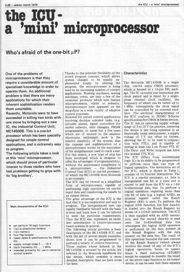
3-28 - elektor march 1979 the ICU -a 'mini' microprocessor
the ICU -a 'mini' microprocessorWho's afraid of the one -bit µP?
One of the problems ofmicroprocessors is that theyrequire a considerable amount ofspecialised knowledge in order tooperate them. An additionalproblem is that there are manyapplications for which theirinherent sophistication rendersthem unsuitable.Recently, Motorola seem to havesucceeded in killing two birds withone stone by bringing out a newIC, the Industrial Control Unit,MC14500B. This is a one -bitprocessor which has been speciallydesigned for simple controlapplications, and is extremely easyto program.The following article takes a lookat this 'mini' -microprocessor,which should prove of particularinterest to those readers who havehad problems getting to grips withits 'big brothers'.
Main characteristics of the ICU:
can perform 16 logic functions1 -bit bi-directional databus1 -bit memoryfour flag outputsmeets Jedec-B specifications for CMOSICssupply voltage range 3 ... 18 Vclock frequency DC ... 1 MHzintended primarily for use in industrialcontrol systems
Thanks to the inherent flexibility of thestored program concept, which allowssystem changes to be rapidly im-plemented simply by altering theprogram, the microprocessor is beingused in an increasing number of controlapplications. Washing machines, sewingmachines, ovens, are only a few of theconsumer products which now featuremicroprocessors, whilst in industry,microprocessors have appeared on theshop-floor in a wide variety of adaptivecontrol processes.However for certain control applicationsinvolving decision oriented tasks, (e.g.intruder alarms, signal controllers formodel railways, slide changers, PROMprogrammers, to name but a few caseswhich are of interest to the amateurelectronics enthusiast) such is therelative simplicity of the system, thatthe expense and sophistication of amicroprocessor would be the equivalentof the sledgehammer used to crack a nut.For this reason, a new type of chip hasbeen developed which is designed tooffer the advantages of programmability,without the unnecessary complexity ofa microprocessor - the IndustrialControl Unit (ICU) or one -bit processor,of which the MC14500B from Motorolais an example.The ICU can be viewed as a simplifiedform of microprocessor, capable ofperforming logic operations on one -bitinput data and transferring the results toan output device.The great advantage of the ICU is thefact that it is uncomplicated and easy toprogram. The inexperienced user canrapidly familiarise himself with the basicsystem and learn how it can be tailoredto meet his particular requirements.Thus the ICU also represents an excel-lent introduction to (micro -)processorbased systems in general.The following article provides a basicdescription of the MC14500B ICU, andwith the aid of several simple examples,shows how it can be programmed toperform a variety of control functions.Those readers whose interest in theMC14500B is aroused by the article, arereferred to the Motorola handbook forthe device, which contains a moredetailed description than we have roomfor here.
Characteristics
The Motorola MC14500B is a singlechip, one -bit static CMOS processor,which is housed in a 16 -pin DIL pack-age. The IC executes one instruction perclock period and is timed by a single-phase internal clock oscillator, thefrequency of which can be varied up to1 MHz. Alternatively the clock signalcan be controlled by an external oscil-lator. The electrical characteristics ofthe ICU conform to JEDEC B -Seriesspecifications for CMOS B -Series devices.The IC has an operating supply voltagerange of 3 to 18 V (in practice, assumingthe device is not being operated in anelectrically noisy environment, a supplyvoltage of 5 V can often be chosen,allowing the IC to be used in conjunc-tion with TTL), and is capable ofdriving at least one Low Power TTL IC(the Data- and Write outputs can drivetwo normal TTL ICs).The ICU differs from conventionallogic ICs in its ability to be programmedto perform more than one type oflogical operation. The instruction set ofthe ICU, which is shown in Table 1,consists of 16 four -bit instructions. TheICU is a one -bit processor, i.e. data ismanipulated one bit at a time and isrouted to and from the ICU via a 1 -bitbi-directional data bus. To perform alogical operation requiring more thanone bit of data (e.g. a logical AND), aninternal register called the ResultRegister (RR) is used. To perform thelogical AND function, the first data -bitis loaded into the Result Register bymeans of a LOAD instruction. The ICUis then supplied with an AND instruc-tion, and the second data -bit is readonto the bi-directional data buswhereupon the logical AND operationis performed on the data present inthe Result Register with the datapresent on the data bus. The result ofthis operation becomes the new contentof the Result Register (which alwaysreceives the result of any of the ICU'slogical operations, hence its name).Since a third instruction (STORE)would be required to transfer the resultof the above logic function to an outputdevice, it can be seen that three separate
the ICU - a 'mini' microprocessor elektor march 1979 - 3-29
operations are needed to simulate a two -input AND gate (see figure 1).Like a microprocessor, the ICU operateson the stored program principle. Theinstructions to be executed by the ICUare normally stored sequentially in thesystem memory. However, in addition tothe ICU's op -codes, the memory mustalso contain the address of the data tobe loaded into the Result Register, orthe address of the latch onto which thecontent of the Result Register is to bestored. The addresses are decoded byinput and output selectors - as shownin the block diagram of figure 2.Once again, let us take the example of alogical AND function being performedon two input signals A and B, which are
present at inputs 1 and 5 respectively ofthe input selector, and assume that theresult of this operation is to be storedon output 9 of the output latch. Whenan address is presented to the input oroutput selector the corresponding inputor output is connected to the data lineof the ICU. Thus the AND operation isperformed as follows:
1) The system memory provides theICU with the LOAD (LD) instructionand supplies the input selector withthe input address. The logic level ofthis input is then transferred via theICU's one -bit data bus to the one -bitResult Register.
2) The ICU fetches the next instructionfrom system memory - the ANDinstruction - whilst the input selectoris supplied with the address of in-put 5. The addressed input data isdemultiplexed onto the ICU's dataline and then is logically `ANDED'with the data in the Result Register.The original contents of the ResultRegister are lost.
3) Finally, the ICU is provided with theSTORE (STO) instruction, whilst theoutput selector is presented with theaddress of output latch 9. The datain the Result Register is then trans-ferred to this output latch via thebi-directional data line.
Figure 1. This figure illustrates the differencebetween dedicated logic devices and the(programmable) ICU. The conventional logicgate requires only a single operation to ex-ecute the function. The ICU on the otherhand requires three separate operations toperform the same task.
Figure 2. Block diagram of a basic ICUsystem that is clocked by hand.
Table 1. Instruction set of the ICU.
Table 1Instruction Code Mnemonic Action
#0 0000 NOPO No change in registers. R -4R, FLGO 4- _FL#1 0001 LD Load Result Reg. Data - RR#2 0010 LDC Load Complement Data -4 RR#3 0011 AND Logical AND. RR D -4 RR#4 0100 ANDC Logical AND Comp!. RR D -4 RR#5 0101 OR Logical OR. RR + D -. RR#6 0110 ORC Logical OR Compl. RR + D -.RR#7 0111 XNOR Exclusive NOR. If RR = D, RR - 1#8 1000 STO Store. RR - Data Pin, Write.- 1#9 1001 STOC Store Compl. RR -. Data Pin, Write.- 1#A 1010 I EN Input Enable. D -4. IEN Reg.#13 1011 OEN Output Enable. D -. OEN Reg.#C 1100 JMP Jump. JMP Flag 4- __EL#D 1101 RTN Return. RTN Flag.- _J-1_. , Skip next inst.#E 1110 SKZ Skip next instruction if RR = 0#F 1111 NOPF No change in Registers RR -4 RR, FLGF .-SL
3-30 - elektor march 1979 the ICU - a 'mini' microprocessor
Program Memory and ProgramCounterOne of the advantages of an ICU -basedsystem is that the number of inputs andoutputs can be expanded virtually adinfinitum, providing the memory issufficiently wide to address theI/O ports. The Program Counter (PC)supplies the system memory with theaddress of the instruction to be ex-ecuted. The PC will normally count upto its highest value and then 'wrap-around' to zero and start counting upagain. Thus the sequence of instructionsin memory can be repeated, providinga 'looping' program.
Minimum systemFigure 3 shows the circuit of a mini-mum ICU -system based on the blockdiagram of figure 2. The system has8 inputs and 8 output latches. IC3 is aspecially designed type of multiplexer-demultiplexer, which, like the ICU, hasa bidirectional data line. Thus, the ICUcan not only write data onto an outputlatch, it can read data off it as well.Both the desired instruction and theappropriate address are set up on adual -in -line switch. In this case, theclock signals are provided by hand, bydepressing the pushbutton switch S 1.Care should be taken to ensure thatonly one clock pulse is given at a time,lest the ICU execute a particular instruc-tion several times in succession.The state of the Result Register, dataline, etc. can be displayed by means ofLEDs, which are connected via buffersto the most important points in thecircuit. If things threaten to get out ofhand, S2 takes the reset pin of the ICUhigh, clearing all registers and resettingthe FLAG outputs.With a four -bit address word, up to16 locations can be selected; in this case8 inputs and 8 outputs. The highestaddress bit, A3, is used to control theChip -Enable (CE) inputs of IC2 andIC3, and hence switch between inputand output lines. In conjunction withthe Write signal of the ICU, A3 ensuresthat only one device, be it IC2, IC3 orthe ICU, has access to the data line atany given time.The basic design of the system shown infigure 3 bears a close resemblance tothat of larger microprocessor -basedsystems, which also contain a data busand address bus shared by a largenumber of ICs.With the practical circuit of figure 3, letus see how one would actually executethe above example of a logical ANDfunction. As we have seen, the programfor an AND operation is:
1. LOAD A2. AND B3. STORE C
The op -code for these instructions canbe found by looking up the instructionset of the ICU in Table 1.First, however, we must ensure that A ispresent at input 1, B at input 5 and that
3
DUS
ClockSi
N5$4 15
61 3 16 9 10 11
CE D ADD A2 AlAo
IC2VEE 4051'vss0 3 4 5 6 7
31 14 15 12 1 5 2 4
0 0 01 2 3 4 5 6 70 0 0 0
IN -1:21" L
L
Ni. N3 = IC4 = 4071
N5 N8 = 2/3 IC 6=4049
S2
sL98/
7 x LED
47k
16
X2clock
clockout
¢1
instr. r.
1 3I i2T 111 io*A31A2 4.1
8 switches
e- 471=1-
16
4 5
13 12 11 10
IC114500
D write
e--- 4 7=-:_c,
,=
N7
4012
3 10 18 7 B 5 N8-D wi A2 A
wo IC314599
reset0 1 2 3 4 5
1 12 13 14 15 16 17
Ao
CE
6 7
89 A BC DE F0 0 00000OUT -11W
13 12 11 t0
c c
IC5ULN2003XR 2203MC 1413SN 75478
79049 3
3
C is stored on output 9. In this case theaddresses of these locations are simplythe binary equivalent of 1,5 and 9, i.e.0001, 0101 and 1001 respectively. Thusthe DIL switch should be set as follows:1) 0001 0001 - whereupon a clock
pulse is applied (A istransferred to RR)
2) 0011 0101 - another clock pulse(A B = C)
3) 1000 1001 - another clock pulse(C is transferred to out-put 9)
Step by step, therefore, the procedure isas follows:
The four right-hand DIL switches are setto address (in binary) 0001, with theresult that on the next clock pulse,input 1 of IC2 is connected to the dataline of the ICU. By means of e.g. a wirelink, this input should be connected tologic 1. Once the four left-hand switcheshave been set to the instructioncode 0001 (= LOAD), Si should bepressed, taking the clock signal at pin 14of the ICU low and extinguishing theclock signal indicator LED. On thenegative going edge of the clock signal(the clock signal was previously high)the ICU latches the LOAD instruction
the ICU - a 'mini' microprocessor elektor march 1979 - 3-31
into the Instruction register, and uponS 1 being released and the clock signalbeing returned high, the data on thedata line is read into the Result Register.Since the data line is high, a 'I' is readinto the Result Register, causing thecorresponding LED to light.The second instruction (0011 = AND)and second address can now be pro-grammed on the DIL switch. Since thesecond instruction is an AND operation,input 5 should also be taken high. Assoon as the clock signal is taken low,input 5 will be connected to the dataline and the ICU will read the ANDinstruction into its Instruction Register.The data line LED should light at thisstage. When S1 is released and the clocksignal returns high, the ICU will executethe instruction, and since 1 1 = 1, theResult Register will contain a '1'.
The third instruction differs from thefirst two slightly. Once the op -code ofthe instruction (1000 = STO) and thecorrect address have been programmedon the DIL switch and S 1 pressed, theICU executes the instruction immedi-ately. The only instructions which theICU will execute on the negative goingedge of the clock pulse are STORE andFlag instructions. The Flag instructions(JMP, RTN, FLGO, FLGF) are used toprovide external control signals bysetting pins 9 through 12 of the ICU.These output flags remain active for afull clock period after the negative -going edge of the clock signal.In the case of the STORE instruction,the moment the ICU reads the instruc-tion into its Instruction Register thecontent of the Result Register is put onthe data line and the Write line (pin 2)
4
cl= Programcounter
MEMORY
instruction address
4bits
clock
ICU
DATA
A
0
aaa
1 5 6 7
A 13
4bits
0
8 9 ABCDEF
79049
is enabled (taken high), with the resultthat the logic state of the data line islatched onto the appropriate output(FF9). On the positive -going edge of theclock pulse the Write line goes highagain.The state of the various indicator LEDsat each stage in the above program areshown in Table 2.The above program is a simple exampleof how the ICU can be programmed tosimulate a conventional logic gate.Further examples of programs designedto imitate the function of logic ICs(4 -input AND, NAND, OR, EXOR etc.)are shown in figure 8.As was pointed out earlier, the ICUrequires a number of operations toperform the single function executedby a conventional logic device (e.g.10 program steps are needed to perform
Figure 3. Circuit for a minimum ICU systemwhich is clocked by hand. The instructions tobe executed and the addresses of the data tobe manipulated are set up on the dual -in -lineswitch. The circuit has seven inputs (theeighth is connected to the Result Register ofthe ICU) and 8 latched outputs. The state ofthe data line Result Register and clock signal,as well as selected inputs and outputs can bedisplayed by means of LEDs. The number ofI/O ports can be extended by increasing thenumber of address bits on the address bus.With 8 address bits a total of 256 inputs andoutputs could be used.
Figure 4. Block diagram of a minimum ICUsystem. The basic building blocks of such asystem are:The ICU, which controls the flow of datawithin the system and performs logicaloperations on the data in its Result Registerand data appearing on its 1 -bit bidirectionaldata line.Program memory, which stores the instruc-tions to be executed by the ICU.The Program Counter, which ensures that theinstructions are presented to the ICU in thecorrect sequence.Input and Output Selectors, which decodethe operand addresses stored in memory anddetermine which input or output is connectedto the ICU's data line.
Table 2. This table shows the state of thesystem indicator LEDs at each stage of theAND program. The negative going andpositive going edges of the clock signal(1-0-1) are differentiated to further clarify thesequence of events.
Table 2.
INSTRUCTION CODE DIL Clock (X 1) DATALINE RR input 1 input 5 output 9LD A 0001 0001 1 X X X X X
0 1 X 1 X X load A1 X 1 X X X
AND B 0011 0101 1 X 1 X X X
0 1 1 X 1 X AND with B1 X 1 X X X
STO C 1000 1001 1 X 1 X X X
0 1 1 X X 1 store result in C1 1 1 X X 1
X = 1 or 0, after reset 0
3-32 - elektor march 1979 the ICU -a 'mini' microprocessor
5
5V
load
5V
Li. ADDRESS
0 cm5V 5V
EMI 0
15
3 13 12 45 V ®-
9-preset Is 17 Is Is
enabl4029
up
Clock Bin
Os 06 07 Os6 11 14 2
Cin
5
15
1
preset4n4ble
Clock
3 13 12 4
DATA
[ "L
0 OMINSTRUCTION14500 130_4,
14 13 12 11
4029up
Bin
0 02 03 04 Cout Cin6 11 14 2 7
Aclock14500
5V
0--9
B
14
120 4110 4loo
12 11 10 9
RAY 2112
7 6 5 15 2 3 4
5V
ca 05 V,ADDRESS
14500
- 0A1
14
12 11 10 9
0A2 0A3
A/W 2112
5V
16
7 6 5 15 2 3 4
113
L.
0
write
79049 5
the function of a D -flip-flop). Thus theICU will inevitably take longer toexecute a given logic operation than itsdedicated counterpart. For example,with a clock frequency of 330 kHz, theabove program for a 2- input AND willtake approx. 10µs. However this trade-off in terms of speed is the consequenceof the simplicity and, more importantly,the flexibility of the ICU, which allowsit to be programmed for a wide varietyof different functions.The ability to step through a programone instruction at a time is particularlyconvenient for the beginner who isattempting to familiarise himself withmicroprocessor programming. Howeversuch a procedure is naturally timeconsuming. Particularly for longerprograms, the obvious solution (as isshown in the block diagram of figure 4)is to store the program instructions inmemory and employ a program counterto ensure that they are presented to theICU in the correct sequence. The clockpulses can then be provided by theICU's internal clock oscillator, the fre-quency of which can be set to up to1 MHz (i.e. 1 instruction every I ;is).The circuit of a suitable instruction andaddress memory is shown in figure 5.The instructions and operand addressesare entered by hand into two 256 x 4 -bitRAMs (type 2112). The programcounter, which consists of two 4029's(presettable binary/decade counters)counts from 000 up to 256 and thenstarts from 000 again. The counterincrements by one after each clockpulse and ensures that the contents ofthe next memory location are presentedto the ICU. Thus the program instruc-
tions are executed in the correct se-quence.Instructions are programmed intomemory as follows: The initial contentsof the memory are first erased byclosing the DATA switch, setting switchS2 in figure 3 to the 'run' position, andpressing the 'write' switch. This has theeffect of writing logic '0' into everylocation in memory. The frequency ofthe internal clock oscillator (determinedby the 56 k external resistor) is 330 kHz,which means that the entire memory iserased in approx. 1 ms .Switch S2 of figure 3 should then be setto the 'single-step' position, therebystopping the clock oscillator. The firstprogram instruction accompanied bythe operand address is now set up onthe data lines of the 2112's and writteninto the memories by pressing the'write' switch. A clock pulse is thenprovided by hand, incrementing theprogram counter in preparation for thenext instruction to be entered.Once all the instructions have beenstored in memory the program can berun simply by switching S2 to the 'run'position. Of course it is also possible tocontinue to provide the clock pulses byhand, stepping through the programone instruction at a time, and checkingthe state of the program by means ofthe LEDs. To this end the second DILswitch and the 'load' button have beenincluded.When entering a program the programcounter is incremented at each instruc-tion, thus a program containing e.g.5 instructions would leave the programcounter at 005. If one then wantsto step through the program by
hand, it would involve supplying256 - 5 = 251 clock pulses until theprogram counter 'wrapped round' to thestart of the program. With the aid of theDIL-switch and 'load' button, thisbecomes unnecessary. One simply setsup the address of the first instruction(e.g. 0000 0001) on the DIL-switch andpresses the 'load' button. The programcounter is then set to that address.By adding additional LEDs with ac-companying buffers (ULN 2003) it is asimple matter to display the state of theprogram counter and contents of thememory at any given moment. Ifdesired, one could also use 7 -segmentdisplays, or - perhaps the best idea ofall - link the entire system up to anexisting microprocessor system; figure 6provides a simple interface circuit forlinking an ICU system to the SC/MP.The display and the keyboard of theSC/MP system can then be used to readdata into and out of the ICU systemmemory. A further advantage of thisarrangement is that the cassette dumproutine of the SC/MP can be used tostore programs for the ICU system. TheICU represents a useful extension to theSC/MP system, since it can be used toassume a number of simple controltasks, freeing the microprocessor formore complex operations.
Enabling Instructions - IEN OENBefore proceeding to examine anexample of a program which can be runon the above -described system, it is firstnecessary to take a look at two ICUinstructions which are of prime import-ance: IEN and OEN.
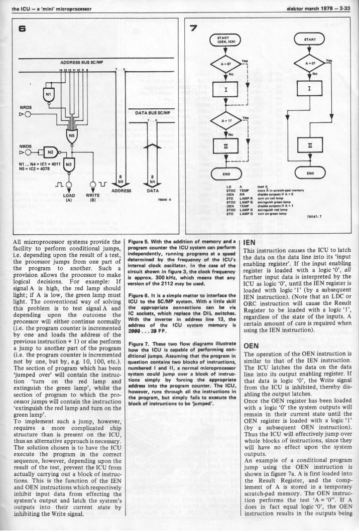
the ICU - a 'mini' microprocessor elektor march 1979 - 3-33
6 7
ADDRESS BUS SC/MP
10 13 12 11
NRDS
>0
N1
NWDS
MDN1 ... N4. IC1 - 4011N5 = IC2 = 4078
a;
n0LOAD
(Al
8
bitO1-1
ADDRESSWRITE
(E0
DATA BUS SC/MP
7 0
DATA
79049 6
AU microprocessor systems provide thefacility to perform conditional jumps,i.e. depending upon the result of a test,the processor jumps from one part ofthe program to another. Such a
provision allows the processor to makelogical decisions. For example: Ifsignal A is high, the red lamp shouldlight; if A is low, the green lamp mustlight. The conventional way of solvingthis problem is to test signal A anddepending upon the outcome theprocessor will either continue normally(i.e. the program counter is incrementedby one and loads the address of theprevious instruction + 1) or else performa jump to another part of the program(i.e. the program counter is incrementednot by one, but by, e.g. 10, 100, etc.).The section of program which has been`jumped over' will contain the instruc-tion 'turn on the red lamp andextinguish the green lamp', whilst thesection of program to which the pro-cessor jumps will contain the instruction`extinguish the red lamp and turn on thegreen lamp'.To implement such a jump, however,requires a more complicated chipstructure than is present on the ICU,thus an alternative approach is necessary.The solution chosen is to have the ICUexecute the program in the correctsequence, however, depending upon theresult of the test, prevent the ICU fromactually carrying out a block of instruc-tions. This is the function of the IENand OEN instructions which respectivelyinhibit input data from effecting thesystem's output and latch the system'soutputs into their current state byinhibiting the Write signal.
START(OEN, IEN/
LO A
STOC TEMPOEN RRSTO LAMP RSTOC LAMP GOEN TEMPSTOC LAMP RSTO LAMP G
load Astore A In stratch-ped memorydisable outputs A 0
turn on red lampifidinpuish green lampP4sable outputs if A = 1eatinguiM red limpturn on preen limp
79047- 7
Figure 5. With the addition of memory and aprogram counter the ICU system can performindependently, running programs at a speeddetermined by the frequency of the ICU'sinternal clock oscillator. In the case of thecircuit shown in figure 3, the clock frequencyis approx. 300 kHz, which means that anyversion of the 2112 may be used.
Figure 6. It is a simple matter to interface theICU to the SC/MP system. With a little skillthe appropriate connections can be viaIC sockets, which replace the DIL switches.With the inverter in address line 13, theaddress of the ICU system memory is
2000 . . . 20 F F
Figure 7. These two flow diagrams illustratehow the ICU is capable of performing con-ditional jumps. Assuming that the program inquestion contains two blocks of instructions,numbered I and II, a normal microprocessorsystem could jump over a block of instruc-tions simply by forcing the appropriateaddress into the program counter. The ICU,however, runs through all the instructions inthe program, but simply fails to execute theblock of instructions to be 'jumped'.
IENThis instruction causes the ICU to latchthe data on the data line into its 'inputenabling register'. If the input enablingregister is loaded with a logic '0', allfurther input data is interpreted by theICU as logic '0', until the IEN register isloaded with logic '1' (by a subsequentIEN instruction). (Note that an LDC orORC instruction will cause the ResultRegister to be loaded with a logic '1',regardless of the state of the inputs. Acertain amount of care is required whenusing the IEN instruction).
OENThe operation of the OEN instruction issimilar to that of the IEN instruction.The ICU latches the data on the dataline into its output enabling register. Ifthat data is logic '0', the Write signalfrom the ICU is inhibited, thereby dis-abling the output latches.Once the OEN register has been loadedwith a logic '0' the system outputs willremain in their current state until theOEN register is loaded with a logic '1'(by a subsequent OEN instruction).Thus the ICU will effectively jump overwhole blocks of instructions, since theywill have no effect upon the systemoutputs.An example of a conditional programjump using the OEN instruction isshown in figure 7a. A is first loaded intothe Result Register, and the comp-lement of A is stored in a temporaryscratch -pad memory. The OEN instruc-tion performs the test 'A = '0". If Adoes in fact equal logic '0', the OENinstruction results in the outputs being
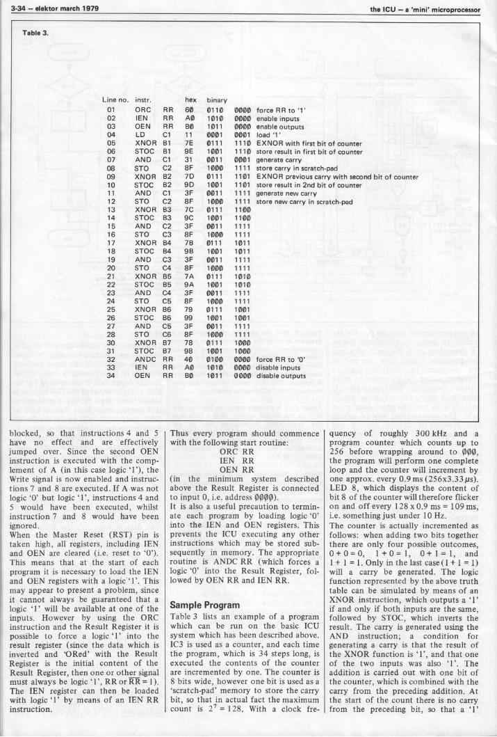
3-34 - elektor march 1979 the ICU -a 'mini' microprocessor
Table 3.
Line no. instr. hex binary01 ORC RR 60 0110 000002 IEN RR A0 1010 000003 OEN RR 80 1011 000004 LD C1 11 0001 000105 XNOR B1 7E 0111 111006 STOC 81 9E 1001 111007 AND C1 31 0011 000108 STO C2 8F 1000 111109 XNOR 82 7D 0111 110110 STOC B2 9D 1001 110111 AND C1 3F 0011 111112 STO C2 8F 1000 111113 XNOR 63 7C 0111 110014 STOC B3 9C 1001 110015 AND C2 3F 0011 111116 STO C3 8F 1000 111117 XNOR 64 7B 0111 101118 STOC B4 9B 1001 101119 AND C3 3F 0011 111120 STO C4 8F 1000 111121 XNOR B5 7A 0111 101022 STOC B5 9A 1001 101023 AND C4 3F 0011 111124 STO C5 8F 1000 111125 XNOR B6 79 0111 100126 STOC B6 99 1001 100127 AND C5 3F 0011 111128 STO C6 8F 1000 111130 XNOR B7 78 0111 100031 STOC 87 98 1001 100032 AN DC RR 40 0100 000033 IEN RR A0 1010 000034 OEN RR BO 1011 0000
force RR to '1'enable inputsenable outputsload '1'EXNOR with first bit of counterstore result in first bit of countergenerate carrystore carry in scratch -padEXNOR previous carry with second bit of counterstore result in 2nd bit of countergenerate new carrystore new carry in scratch -pad
force RR to '0'disable inputsdisable outputs
blocked, so that instructions 4 and 5have no effect and are effectivelyjumped over. Since the second OENinstruction is executed with the comp-lement of A (in this case logic '1'), theWrite signal is now enabled and instruc-tions 7 and 8 are executed. If A was notlogic '0' but logic l', instructions 4 and5 would have been executed, whilstinstruction 7 and 8 would have beenignored.When the Master Reset (RST) pin istaken high, all registers, including IENand OEN are cleared (i.e. reset to '0').This means that at the start of eachprogram it is necessary to load the IENand OEN registers with a logic V. Thismay appear to present a problem, sinceit cannot always be guaranteed that alogic '1' will be available at one of theinputs. However by using the ORCinstruction and the Result Register it ispossible to force a logic '1' into theresult register (since the data which isinverted and 'ORed' with the ResultRegister is the initial content of theResult Register, then one or other signalmust always be logic '1', RR or RR = 1).The IEN register can then be loadedwith logic '1' by means of an IEN RRinstruction.
Thus every program should commencewith the following start routine:
ORC RRIEN RROEN RR
(in the minimum system describedabove the Result Register is connectedto input 0, i.e. address OM).It is also a useful precaution to termin-ate each program by loading logic '0'into the IEN and OEN registers. Thisprevents the ICU executing any otherinstructions which may be stored sub-sequently in memory. The appropriateroutine is ANDC RR (which forces alogic '0' into the Result Register, fol-lowed by OEN RR and IEN RR.
Sample ProgramTable 3 lists an example of a programwhich can be run on the basic ICUsystem which has been described above.IC3 is used as a counter, and each timethe program, which is 34 steps long, isexecuted the contents of the counterare incremented by one. The counter is8 bits wide, however one bit is used as a'scratch -pad' memory to store the carrybit, so that in actual fact the maximumcount is 27 = 128. With a clock fre-
quency of roughly 300 kHz and aprogram counter which counts up to256 before wrapping around to (NH,the program will perform one completeloop and the counter will increment byone approx. every 0.9 ms (256x3.33 gs).LED 8, which displays the content ofbit 8 of the counter will therefore flickeron and off every 128 x 0.9 ms = 109 ms,i.e. something just under 10 Hz.The counter is actually incremented asfollows: when adding two bits togetherthere are only four possible outcomes,0 + 0 = 0, 1 + 0 = I , 0 + 1 = 1, and1 + 1 = 1. Only in the last case ( I + 1 = 1)will a carry be generated. The logicfunction represented by the above truthtable can be simulated by means of anXNOR instruction, which outputs a '1'if and only if both inputs are the same,followed by STOC, which inverts theresult. The carry is generated using theAND instruction; a condition forgenerating a carry is that the result ofthe XNOR function is '1', and that oneof the two inputs was also '1'. Theaddition is carried out with one bit ofthe counter, which is combined with thecarry from the preceding addition. Atthe start of the count there is no carryfrom the preceding bit, so that a '1'
the ICU - a 'mini' microprocessor elektor march 1979 - 3-35
..
r -.0 r , .O .. I. ^
Photo 1. Prototype board for the minimumICU system.
Table 3. Listing of a sample program whichuses IC3 as a counter to make an LED flashoff and on.
Figure 8. The ICU is specially designed toexecute a wide variety of logic functions. Thelogic gates shown here can all be simulated bythe corresponding set of ICU instructions. Asthe example of the D flip-flop shows, evenquite complicated logic operations can beperformed using the ICU.
AND
AND
A
NANDB
LD AC AND B
STO C
LD AAND B
E AND C
AND DSTO E
LD AC AND B
STOC C
LD A
OR C OR B
AEXCL.NOR
B
D Flipflop
C
STO C
LD AC XNOR B
STO C
LD AC XNOR B
STOC C
LD AB STOC B
ORC RROEN RRLD old clockSTO temp
LD clock
STO old clock
ANDC tempOEN RRLD DST Q
79049 8
must first be presented to input 1. If a'0' were at this input, the circuit wouldsimply add zeroes and the output of thecounter would never change.The operation performed by theprogram can be expressed by the fol-lowing equations:Sn = Bn + Cn and Cn + 1 = Sn Bn(where S = Sum, B = Bit, C = Carry andn may equal 1 ... 7)Thus Bit 1 '1'
Carry 1 + '1'Sum 1 '0'
Carry 2 = Sum 1 Bit 1
='1' 'I'= '1'
As a further illustration of the type ofprogramming required, figure 8 listsseveral short program sections that canbe used to simulate standard logicfunctions.
Lit.:Motorola Industrial Control UnitHandbook. (Available from Motoroladistributors.)
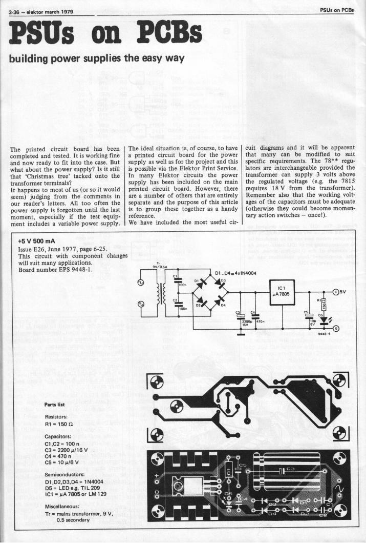
3-36 - elektor march 1979 PSUs on PCBs
PSUs on PCBsbuilding power supplies the easy way
The printed circuit board has beencompleted and tested. It is working fineand now ready to fit into the case. Butwhat about the power supply? Is it stillthat 'Christmas tree' tacked onto thetransformer terminals?It happens to most of us (or so it wouldseem) judging from the comments inour reader's letters. All too often thepower supply is forgotten until the lastmoment, especially if the test equip-ment includes a variable power supply.
The ideal situation is, of course, to havea printed circuit board for the powersupply as well as for the project and thisis possible via the Elektor Print Service.In many Elektor circuits the powersupply has been included on the mainprinted circuit board. However, thereare a number of others that are entirelyseparate and the purpose of this articleis to group these together as a handyreference.We have included the most useful cir-
cuit diagrams and it will be apparentthat many can be modified to suitspecific requirements. The 78** regu-lators are interchangeable provided thetransformer can supply 3 volts abovethe regulated voltage (e.g. the 7815requires 18 V from the transformer).Remember also that the working volt-ages of the capacitors must be adequate(otherwise they could become momen-tary action switches - once!).
+5 V 500 mAIssue E26, June 1977, page 6-25.This circuit with component changeswill suit many applications.Board number EPS 9448-1.
Parts list
Resistors:
Al = 150 E2
Capacitors:
Cl ,C2 = 100nC3 = 2200 µ/16 VC4 = 470 nC5 = 10 µ/6 V
Semiconductors:D1,D2,D3,D4 = 1 N4004D5 = LED e.g. TI L 209ICI = µA 7805 or LM 129
Miscellaneous:
Tr = mains transformer, 9 V,0.5 secondary
T.
9V/ 0,5A
DI D4= 4x1N4004
03
9448 , 4
4,A) 00
0,0 0-11-p
S= Liimmi 0 P 0 J 0 0-1f,-4°
5V
O
PSUs on PCBs elektor march 1979 - 3-37
+15 V 250 mA and -15 V 250 mAIssue E42, October 1978, page 10-38.Originally designed for the Elektor TVscope but very useful where op -amps areused.Board number EPS 9968-5a.
D4=1N4001
Parts list
Capacitors:C1,C2 = 470 µ/35 VC3,C4 = 100 nC5,C6 = 1 µ/25 V tantalum
Semiconductors:ICI = 7815IC2 = 7915D1 ... D4 = 1N4001
Miscellaneous (not on p.c. boardproper, see figure )
Tr1 = mains transformer,2x 18 V/250 mA
S1 = double -pole mains switchF1 = fuse, 100 mA
15V
15 V
9968 14
+15 V 1AIssue E31, November 1977, page 11-37.Board number EPS 9218b, limited stocksstill available, price £ 1.05.
7,1
Parts list
Capacitors:C1 = 2200 µ140 VC2,C4 = 100 nC3 = 470 µ/16 V
Semiconductors:ICI = 7815
= 4 x 1N4004
Miscellaneous:
Transformer with 24 V/1 Asecondary
B=4x1N4004
CI' C2
MOP40v
ICI7815
470/./)6v
9E150 4a
15V
C
3-38 - elektor march 1979 PSUs on PCBs
Symmetrical ± 5-15 V 1 AIssue E15/16, July/August 1976,page 7-63.Board number EPS 9637, limited stocksstill available, price £ 0.80.
P
Cj
IC1741
IC2 °"11 78G
COM CONT
C2P0i5 15V 1A
22
4j100,,
2
COM CONT P2
IC3 22k
79G 40VN4
OUT 0096375 15v 1A
rf.
L(731-41-1)-4\-It5)42.
+12 V, +33 VIssue E19, November 1976, page 11-15.(Albar).Board number EPS 9437.
Parts list
Resistors:
R1 = 1 E2R2 = 3k3R3 = 4k7Rx = see text
Capacitors:
C1 . C4 = 100 nC5 = 2200 µ/40 VC6 = 47 4/10 VC7 = 100 p
Semiconductors:T1 = BD 241A, MJE 3055D1,D2 = 1N4002, BY 188IC1 = 723
Miscellaneous:
Tr = Transformer, 24 V/1.5 ANiCad Accumulator, 18 V
(see text)
Ni Cad+0 0- 0____110
C3 ICle1011C1 ri
caCl C2
C6R 3 ICIS
-9- c7Q OL
D2 Wee"+33V
0
PSUs on PCBs elektor march 1979 - 3-39
+30 V 2 A and -30 V 2 AIssue E18, October 1976, page 10-45.Outputs independantly variable.Board number EPS 9004.
Parts list
Resistors:
R1,R2 = 47 52R3,R4 = 0.33 W2 WR5 = 71k5R6 = 3k3, 1 WP1 = 100 k lin.P2 = 47 k lin.
Capacitors:
C1,C2 = 4700 p, 35 VC3,C4 = 1 nC5,C6 = 100 µ, 35 V
Semiconductors:IC1 = RC 4194 (Raytheon)T1 = TIP 2955T2 = TIP 3055T3,T4 = BC 140-10, 2N1711D1 = LEDB1 = B8005000 (80 V, 5 A)
Various items:Tr = mains transformer,
2 x 22 V/2 A
2x22 V -2A 131 = B8005000 145
o.l=1
41,3035V
7, TIP2955
(47
LEO
c3 e0140 -3o
C7 47004,35V
R2
BC140-10
N,
TIP3055
iC1 -13C4194TK
R5
COT-P.5In 021
47k
35v T min 50 mymax. 30 V
3-40 - elektor march 1979 PSUs on PCBs
+0 10 V 300 mAIssue 27/28, July/August 1977, page 29.Board number EPS 77059.
20V E)0-
;T3
CS CL
sr
1C23130
0
0137iTIP31
Q 10V
IC.
(L)11059
+5 V 3 A and -12 V 500 mAIssue E35, March 1978, page 3-09.Originally designed for the SC/MP andwould suit many microprocessor sys-tems.Board number EPS 9906.
B400800
PSUs on PCBs elektor march 1979 - UK 15
9906
OED
IWO191,911,4M91=4O1,010,11
G ML,1Ammine"---lED
sememsa.melwrAmm =mdi-msm.---im
am '
Vflmo °Si' fiLD\66) c.°aw.aDmis
--0 Il. jL_
ID C6
aa
a.
aaa
a
U
U
0C
1 0 0O 0O 0O 0000O 0
0000
320
0
Parts listSemiconductors:
Resistors: IC1 = 723R1,R4 = 2k7 Capacitors: IC2 = 79G Miscellaneous:R2 = 8k2 C1 = 2200 µ/25 V (see text) T1 = BD 137, BD 139 Tr1 = Transformer 12 V,R3 = 100 12 C2,C3 = 100 n T2 = 2N3055 3 ... 4 A secondaryR5 = 0.18 51/2 W (see text) C4 = 1 n B1 = 840 C5000 40 V (see text)R6= 180 12 C5 = 10 µ/16 V 5 A bridge rectifier (see text) Tr2 = Transformer 15 V,P1 = 2k5 C6 = 1000 µ/25 V B2 = B40 C800 40 V 0.5 A secondary (see text)P2 = 1 k C7 = 1 µ125 V tantalum 800 mA bridge rectifier Fl,F2 = 300 mA slo blo fuse
UK 16 - elektor march 1979 market
Ipssinglinki
Modifications toAdditions toImprovements onCorrections inCircuits published in Elektor
1/4 Gigahertz counterElektor 38, June 1978, p. 6-01.The sensitivity of the high fre-quency input amplifier (figure 9)can be improved by decreasingR79 to 47 n and inserting a500 a (470 a) carbon presetpotentiometer in series with it;R78 is decreased to 15 k andR84 is replaced by a wire link.
HF
9887 L 1
To reduce clipping of the lowfrequency input amplifier(figure 11) a DUS can be placedin series with both zener diodesD32 and D33.
LF11)R65
9887 L 2
In the parts list D36 is given asa 2V7 zener diode; this should infact be 4V7 as the circuit diagramshows.
Central alarm systemElektor 42, October 1978p. 10-20. On the p.c. board forthe master station (figure 9),pin 3 of IC6 should ideally beconnected to supply common orpositive supply (e.g. pin 1) - wehave often stressed in the pastthat unused inputs of CMOS ICsshould not be left floating! Inpractice it will not normally makeany difference, but if the IC isrunning hot this is almost certainlythe reason.Similary, on the alarm board(figure 8): if either of the twoalarm inputs 'X' and `Y' is notused, it must be connected tosupply common. A floating inputat this point can easily result in`false alarms'!
High accuracy control ofultra -fine torqueFor applying and checking ultra -fine torque values to a guaranteedaccuracy of t 2%, a range oftorque guages is available fromMHH Engineering. The guageshave bi-directional operation andthree scales in either direction foreasy reading from any angle -one on the dial and two (standardand mirror image) on the sleeve.Slave pointers operating in either
direction are standard on bothdial and sleeve. A three -jaw chuckaccepts a wide variety of spindlesand a mechanical stop preventsoverloading. The instruments areideal for checking the torque onpre -loaded bearings, gear trains,watch, camera and instrumentspindles and similar very lowtorque applications. The torquevalues covered are from 10 gf cmto 15 kgf cm (0.1 ozf in to15 lbf in). These guages aremanufactured by the Tohnichicompany of Japan.MHH Engineering Company LtdBramley,Guildford,Surrey,GUS OAJ.England
(1087 MI
Switching power supplywith fanA new dual -output switchingpower supply from GouldElectronic Components Division,the MGD500, incorporates afan -cooling system which enablesthe unit to provide a high powerdensity and also offers the facilityfor mounting in any plane.Designed specifically to powersystems using emitter -coupledlogic, the MGD500 provides twoindependently controlled outputswhich track together, and gives atotal power output of 526 Wfrom a package measuring5 x 8 x 10.5 in (12.7 x 20.3x 26.7 cm).The two d.c. outputs provided bythe Gould MGD500 are 5.2 V(± 0.2 V), adjustable from 0 to80 A, and 2.2 V (± 0.1 V),adjustable from 0 to 50 A, with acommon positive terminal. Inputvoltage can be either 230 V or
115 V (± 15%) a.c., at afrequency of 47 - 63 Hz, and isselectable from the front panel.Regulation is within 0.2% on bothoutputs for a worst -casecombination of ± 15% input and0 - 100% load change. Ripple onboth outputs is 10 mV r.m.s.maximum and 50 mV peak -to -peak (30 MHz bandwidth), andtemperature coefficient is lessthan 0.01% per degC.The Gould MGD500 is protectedagainst overcurrent, overvoltageand overtemperature, and has ahold-up time of 28 ms at full loadin the event of mains failure.Insulation voltage is 2.1 kV d.c.between input and ground and500 V d.c. between output andground, and insulation resistanceis not less than 50 MS/ at 500 Vd.c. The transient response is suchthat the output returns to within1% of its original value within500 ps of a 50% load change.There is no limit on paralleloperation with other units, andunits may be operated in series toa maximum total voltage of250 V. The output voltage can beremotely programmed with a± 5% variation for system marginchecking.Gould Electronic ComponentsDivision,Raynham Road,
Herts. CM23 SPF England
(1034 M)
Telephone line simulatorTelephone lines were originallydesigned for voice transmissionrather than high speed datacommunication, so it is notsurprising that the latter is sub-jected to signal degradation anderrors when transmitted overexisting lines. To assist in thedesign of modems and datatransmission equipment a newinstrument capable of simulatingtelephone line distortions hasbeen manufactured by AxelElectronics Incorporated,New York.Switch -selectable simulation ofstandard line worst -case characte-ristics is possible, and in additionthe instrument can superimposesuch steady-state disturbances asvariable random noise, phasejitter, frequency shifts and
harmonic distortion, as well astransient phenomena includingimpulse noise, phase andamplitude hits, and amplitudedrop -outs. All simulateddisturbances can be selected andvaried individually orsimultaneously.Wandel & Golterman (U.K.) Ltd.40-48, High Street,Acton,London W3 6LG,England
(1089 M)
Solar power panelFerranti Electronics Limited hasdeveloped a new solar powermodule for industrial, pro-fessional and domestic applica-tions.The MST300 series have beendesigned for long life underextremes of environmental andclimatic conditions.The standard module containsthirty-six silicon cells, each3 inches in diameter, seriesconnected to give an output of1.1 amps at 14.4 volts. Itmeasures 560 mm x 480 mm andis only 130 mm deep. Itsaluminium construction offersgood heat sink capability andmakes the module ideal for usein high ambient temperaturezones.
The module is hermeticallysealed to prevent moistureentering the resin filled spacecontaining the silicon cells.Injection of this resin ensuresthat all air is removed frombetween the cover and base plate,an important feature of the designas air pockets have been known tocause premature module failure.A cover of fibre reinforcedpolyester provides protectionagainst the environment includingsuch extremes as sand blasting orultra violet degredation.An additional bonus of the designconcept is the ease with which itis possible to change the moduledimensions. Where necessary,additional silicon cells can beincorporated to meet specificcustomer requirements.Ferranti Electronics LimitedFields New RoadChaddertonOldhamOL9 8NP (1092 M)
market elektor march 1979 - UK 17
Ultra low noisepreamplifierThe SL561C from Plessey Semi-conductors, is a high gain, lownoise preamplifier designed foruse at frequencies up to 6 MHz.Upper and lower cut-offfrequencies can be selected bysingle capacitors and the gainselected between 10 and 60 dBwith a single resistor. Operationat low frequencies is eased bythe small size of the external
1capacitors and the low - noise.
The noise voltage is less than1 nV/N/Hi and the currentconsumption of the circuit is2 mA from a single 5 volt supply.Applications include use withphoto -conductive IR detectors,magnetic tape heads and dynamicmicrophones. It will also replacean op -amp in many applicationswhere a DC response is notrequired.
Plessey SemiconductorsLimited,Chenney Manor,Swindon,Wiltshire,SN2 2QW, England
(1088 M)
High profile DIL switchA special high profile dual in -lineswitch for front panel andthrough panel mounting has beenannounced by Erg Components.The basic version is a 4 -pole2 -way DIL switch that can befinger actuated, or switched byusing a small probe. All wipingaction contacts are gold plated
and specifically designed forhigh reliability µV /µA switching,with a maximum voltage/currentcapability of 240 V AC/2 A (non -switching), 30 V/0.25 A(switching). Custom designversions are also available.Erg Industrial Corporation Ltd.Luton Road,Dunstable,Bedfordshire,L115 4LJ,England.
(1090 M)
New range of miniaturebuzzersNot miniature electronic waspsfrom Scotland but a range ofsmall buzzers being produced byHighland Electronics under thetype number GA 100/K.Emitting a 400 Hz signal with anoutput of 70 - 83 dB (A) at22 cm., they have no movingcontacts and do not cause anyelectrical or R.F. interference.
Current consumption is from16 to 25 mA making themsuitable for use in portable orbattery operated equipmentrequiring an audible warning. Thecase measures 22 x 15 x 10 mmand is made from a high qualityplastic, colour -coded accordingto the four operating voltages of2.5, 6, 12 and 24 volts.Highland Electronics Ltd.Highland House,8, Old Steine,Brighton,East Sussex,BNI lEJ.,England.
(1091 M)
Audio power transistorsA range of epibase and single -diffused TO -220 packaged powertransistors now available fromMicro Electronics Ltd. aredesigned for audio output andswitching applications, withcurrent ratings of 2 A to 7 A andpower ratings of 20 W to 50 W.The devices are available in fourchip configurations for bothamplification and control circuits.
The transistors with epibase chipsare designed for good linearity ofd.c. current gain, have a higherfrequency response (up to 3 MHz),and feature a good safe operatingarea. Both n -p -n and p -n -p
complementary versions areavailable. These characteristicsmake the Micro Electronicsepibase devices ideally suited touse in the output and driverstages of high-fidelity amplifiers.The range of single -diffusedtransistors available from MicroElectronics Ltd. are characterisedby a distinct safe operating area,and are more suitable for use involtage regulators, solenoiddrivers, and low -speed switchingand control circuits.Micro Electronics Ltd.,York House,Empire Way,Wembley,Middlesex.England
(1093 MI
Digital Gauss/flux meterRLF Industries has announced anew magnetic -measuringinstrument, used for measuringboth flux density and total flux.The model 906 Portable DigitalGaussmeter/Fluxmeterfor use in the laboratory, inproduction, or in field locations.When operating in its gaussmetermode, the instrument uses probesbased on the Hall effect. A widerange of transverse and axialprobes is available from RFL.
Built-in axial and transversereference magnets provide overallaccuracy better than 3%. Full-scale ranges of 1000 and 10,000gauss provide resolution of 1 and10 gauss, respectively. Capabilityfor 100% overrange provides formeasurement up to 20,000 gausson the instrument's 3-1/2 digitliquid -crystal display.As an integrating fluxmeter, theModel 906 provides ranges of10' and 10' maxwell-turns.Probes required for measurementsin the fluxmeter mode areavailable from RFL, or the usermay fabricate his own as the needarises.The model 906 operates fromeither 115- or 230 -volt, 50-60 Hzpower, or from its internal gel -eel(TM, Gould, Inc.) battery whichis included for field operation. Acharging circuit is included. The
Gaussmeter/Fluxmeter isprovided with an impact -resistantplastic case equipped with acarrying handle which serves alsoas a tilt bail to position the
. instrument for easy viewing. Sizeis 8-1/2" wide by 3" high by9-1/2" deep (21.6 x 7.6 x 24 cm).Weight is 4 lbs, 6 oz. (1.95 kg).RLF Industries, Inc.Boonton,New Jersey 07005, U.S.A.
(1094 M)
Quad bi-fet switchPMI's new quad Bi-FET switchesdeliver high-performance butwithout the problems that plaguecompeting CMOS products.
Because these devices employBi-FET rather than CMOSprocessing they are naturallyimmune to static blow out. Nospecial handling is ever required.Nor is there any danger of SCR -type latch up problems.Available in both normally -open(SSS7510) and normally -closedversions (SSS7511), each ispackaged in a 16 -pin, hermeticDIP. They are pin -for -pin replace-ments for the Analog DevicesAD7510DI/AD7511D1.'On' resistance at 75 ohmsmaximum is low. In addition,high 'off isolation, low crosstalkand low leakage currents makesthese quad switches ideally suitedfor a variety of applications.The SSS7510/SSS7511 areexcellent choices for pro-grammable active filters, pro-grammable -gain amplifiers andposition controllers. They are alsosuitable for chopper, demodulatorand general-purpose switching andmultiplexing applications.Digital inputs are TTL and CMOScompatible. Break -before -makeswitching is guaranteed - withoutthe need for external pull-upresistors.Precision Monolithics, Inc.1500 Space Park DriveSanta Clara,California 95050,U.S.A.
(1095 MI
Elektor March 1979 - UK 20 advertisement
Here's whyyou should buyan ICE instead
of just anymultimeter
* Best Value for money.*Used by professional engineers, D.I.Y.
enthusiasts, hobbyists, service engineers.* World-wide proven reliability.* Low servicing costs.* 20K/ volt sensitivity and high accuracy.* Large mirror scale meter.* Fully protected against overload.* Large range of inexpensive accessories.*12 month warranty, backed by a full after
sales service at E. B.Sole U.K.Distributors.
Prices from £16.60 -£32.00 + VAT
I =I
I.C.E.ELECTRONIC BROKERS LIMITEI5149-53 Pancras Road, London NW1 20B.Tel: 01-837 7781. Telex; 298694.
Please send me full colour leaflet and prices on whole ICE range includingaccessories.
Name
Ifdress ELJ
LINES FROM OUR VAST STOCKS - IMMEDIATE DELIVERY
All below manufacturers' prices all newstocks. Quantity discounts -export enquriesinvited. POS. tag! & Packaging 35p per order.CALCULATOR CHIPS General instrumentGIMT4 on anti -static foam 24 pin DIL socketfor use with Bowmar display (1.50 ea. Packof 25 chips E25. 100 for E80. 500 for E350.BOWMAR 9DIGIT CALCULATOR displaywith PC connector 0.2digits. Commoncawothlodc8e5with red bezel f 1.25 -ea. 10 for £10.
TEXAS 19 gold plated snap he contact ongold plated PC board. Size 70x80x2mrn 75pORP12 light dependent resistance (Eel_RPY30i 2 for £1 10 for E4. 100 for £35.FAIRCHILD END10 0.15 7 se g display. Ccathode 50p, 10 for E4.50. 100 for 740.TBA 120A T.V. IC amplifier Siemens 750.10 for E6. 100 for £50. 1000 for E350.BECKMAN 500 kcs. Triggerable clockingoscillator for use with calculator chips 5v
Bull1R1110'2crr8,Eltlg2.3,20c1crurgdisplay 7 segment 0.25 digits. Neon typewith red bezel socket and data. E1.95.10 for f17.ALMA PUSHBUTTON high reliability reedswitches. Push to make. 18x27x18mm 40010 for (3.50 100 for f33.00.SMITHS INDUSTRIES Audible warningdevices 6.12 volts. 2 transistors 30 alOmm
;i:311,FtVelljtcrL15_0P,1011,1411135DIECT3E°630°8integral amplifier 8v D.C. £2.50 ea. 10 forE20 100 for E175.OSMOR CHANGE OVER REED RELAY12o coil 20m/a operating current59x17x13rnm 75.p ea. 10 for f5, 100 for£45, 1000 for £400.MARRIOTT TYPE HEADSQuarter Track all at 50% discountYy44 fool pr,10044 100SRP5111)(Wile
RECORD:REPLAYRECORDIREPLAY
4300(400
(20(3000
(15000am pp
%ES. ERASE (125 (1000 MOO
MULLARD AD161 A0162 MATCHEDPAIRS
10 Pair 10{' :"..x.r 500 PairEl pair f8.00 (300.00
Cartons of 600 pairs (350.00 EX STOCKSOLDER Imulticore type) Survicol 10metres for 0, 50 metres for f4 100 metresfo E7.RAC rP,TION DETECTORS Quartz FibreDosimeters. Pen type with clip with lens andscale 0.50R. Originally over f5 OURPRICE 95p EACH. 10 for f8, 100 for £60.1000 for £500.CLOCKING OSCILLATOR (Pye Dynamics),thick film 1mHZ supply 5v 19x25x8mm
TZV TUNERS f forry G.E.C.f(11°H°F 3gforr,,s-%.£7?e3%x2%xl% E2.50 ea. 10 for E2of, 100 for£175 500 for £750. 1000 for £1250.
T.V. SOUND TUNER KIT Through yourF.M. tuner. Kit of parts with instructionsE550. Ready built, tested (7.00.
JOYSTICK CONTROLS (Ideal for TVGames, model control) sturdilyconstructed compact givong full 360movement and control. Each unit fitted4 -off 100K linear controls, Pair E4.00T4,0F LONG, MEDIUM & F/M TUNER5 -BUTTON SELECTOR SWITCHESINPUT SELECTORS FOR GRAM ANDTAPE Supplied with FRONT-ENDTUNER AND FERRITE AERIALSIMPLE CONNECTIONS 19x13x6cm withdata and circuit. Some Darts missingonly E2.50 each.POWER UNIT KIT FOR ABOVE MODEL25/28 VOLTS E2.95.MULLARD TUNER MODULES with dataLP1171 combined AM/FM IF strip E3.50LP1179 FM front end with AM tuning gangpused with LP1171 -£3.50. LP1171 and 79
air 10 pairsif50. 100 pairs for
CA3085 RCA POSITIVE VARIABLEREG. 5 volt 100 m_amp variable 1.8.24s55p.ea. 1015. 100135. 1000/300MULLARD LP1157 AM TUNERMODULES WITH CIRCUIT E2.50 each101E20 100(1752N3055A TO3 POWER 80 VOLTVERSION. 10 for E2.50, 100 for (2200
TRANSISTORS BY MULLARD TEXASFAIRCHILDPrice per 10 100 500 1000AC 128 0.230 0.200 0.180 0.150AD149 0.750 0 650 0.550 0.490AD161 0.380 0.330 0.290 0.250AD162 0 380 0.330 0.290 0.250BC107 0 100 0.085 0.075 0.065BC109 0.110 0 095 0.080 0.070BC109C 0.120 0.100 0.085 0075BC114 0_080 0_065 0.050 0.040BC132 0.080 0.065 0.050 0.040BC153 0.085 0070 0.055 0.045BC172 0.075 0.060 0.050 0.040BC173 0.075 0060 0.050 0040BC205 0.070 0.055 0040 0.035BC208C 0.075 0060 0050 0040BC209 0.075 0.060 0.050 0.04060181 0_600 0.500 0.440 0.400BD182 0.700 0600 0500 04408E181 0.240 0200 0.185 0 160BEN'S° 0.180 0.160 0.140 0_125BEY51 0.180 0.160 0.140 0 125BFY64 0.220 0.195 0.175 0.150BF Y90 0.750 0.680 0.630 0.550BU205 1.000 0.900 0.800 0.750BU208 1.250 1.100 1.000 0.900BY127 0.110 0.090 0075 0065
0400 0.330 0300 0 260LM311H 0.700 0600 0.550 0.500TBA625I3X5 0 680 0.600 0 550 0 500
Ir MENRysRADIO
All mail toHenry's Radio404 Edgware RdLondon W2 EnglandPhone 101) 723 1008
HIGH PERFORMANCEPOWER SUPPLY KIT
Zero - 30v 5mA 1.5A current limit0/P resistance !mil tat board 01P)
Norse/ripple< . Very sharpcurrent limit
Ideal lab standard PSUGenerally idiot proof
Kit of parts/F/G pch tinned,transformer controls, wire all
components £11 + 8%Schools and Colleges £10 +8%
P&P 70p
40k H7 Ultrasonic Transducers£2/pair (15p)
Audio Amp I.C. p A706 i8A641B5w 12v 4E2 £1 (15p)
Vernitron 10_7m CeramicFilters 65p (15p)
455 kHz CeramicFilters 50p (15p)
Mono Cassette Amp,"OSC,Boardwith Circuit £1.30 (15p)
Stereo Cassette Deck TopLoading £9 (60p)
Tun TransistorsZTX type unmarked £5/100
RCA 3055 type EXEOPT 35p
2N3773 £212501CR25 Resistors 1/3w
E12 £6/1000 (30p)LM107 OP.amp sim.307'741(compensated 301 hut nooffset null pins) 20p (10p)
Sprague 30A mainsRFI Filter £4 (60p)
Papst Fan 4'h"x4./,"x2"100 c.f.m. £3.50 (80p)
Humidity Switch Adjustable50p (15p)
Air p0peiated Switch£1 (25p1
Mains Latching Relay 80p (20p18 pin Octal Relays
12v 24v 110v DC coil11 pin Octal Relays £1 ea (25p)24v 48v DC coil115v 240v AC coil
Bead Thermistors N.T.C. Res Cci) 20 C250R 1k2 20k 220k 1m4 60p (10p)
Transformers 12v 10A £5 (90p) 24v10A £6 (Cl). 9v 3A £1.60 (60p1.20v 1A Toroid 3 dia x 1 £2.25(30p). 6.0 6v 250mA £1.10 120p).6v 500mA £1.10 (20p). 18v 2.5A£2.25 (35p). 12 + 12v 36VA£2.25 (60p). 12v 4A £2.30 1650)15.0 15v 36VA £2.25 (60p).
t ELECTROLYTICS4700p 25v 50p (15p)4700p 40v 500(150)15.000p 50v £1.25 (60p)1000p 63v4700p 63v
8205pp )(1122pp))
Toroid 0-30-36v 4AE.S. £5 (50p)
1p 600v Paper Cap 65p (15p)Ideal for Electronic IgnitionCONVERGENCE POTS
5E2 10)2 50E2 200E2 £51100 14001W.W. RESISTORS
0.1E2 1% 10w 20p0.352 1% hIsinkresistor 25w 25p
P&P shown in bracketsmin. order £2
Add 121/2% VAT to items marked tOthers 8%
KEYTRONICS332 LEY STREET, ILFORD, ESSEXShop open Mon Sat 9 30 am 2pm
Telephone 553 1863
74109 259TTL * /4118 75p/400 10p 74120 80p7401 104 74121 25p7402 10p7403 10p 14122 35p7404 74123 40p12o/405 74125 35p12p/406 74126 359259/407 741 28 60p25P7408 74130 120p12p/409 12p /4131 9047410 74132 45p12p14117412
74135 90p15p 74136 80015p7413 26p 74137 9047414 45p /4138 1004/416 250 74141 50p
7417 74147 180p25p7420 12p /4147 270p7421 70144 270p2047472 15p 74145 55p
/423 200 74147 10134
7425 20p 74148 90p
7426 22p 741513 6697427 22p 74151 45p
7428 74151 45p2597430 /415.4 70p12p7432 74155 4547097433 74156 45928p7437 20p 74157 4Sp
7438 20p 74160 55p
7440 12p 74161 55p
/441 k 45p 74162 559
7442 004 74163 569
7443 74164 60460p7444 60p 74165 600
7445/446
74166 759658,
74167 16045047447 74170 100p50p74487450
74173 80p5E2 741 74 60912p
7451 74175 60p12p7453 74176 50,1247454 12p 74177 SOp
7460 *178 75912p7470 78179 12042597472 74180 9042047473 74181 130p2597474 259 74182 5047475 74184 12042697476 25p 74185 100p
7480 74188 3204401,
7481 135p74190 70p
7482 759 74191 70p
7483 754 74192 6047484 70p 74193 6007485 604 74194 559
7086 254 74195 50p7489 1300 74196 5134
7490 74197 6042597491 404 74198 1009
7492 369 74199 1004/49J 30p 74293 90p7494 70p 74LS00 19p
7495 469 7451'2 804
/4967497
469120p
7005 100p7817 100p
74100 80p7815 100,
74104 404 /818 100p74105 40p 7824 1001,741077410E1
2591004
74166 75p
LINEARAY 38500 480p NE556 904CA3039 70p NE5628 4000CA3046 60p SAD1024 15000CA3060 7259 SL91713 0504CA3065 200p 5N76003N 1504CA3076 7500 59760139 1109CA3060 759 5/476013ND 1254CA3084 21500 SN76023N 1109CA3085 850 6976013ND 125pCA3086 SN76033N 1504CA30138 19909 59767779 1604CA3089 160p 57476729N la0004309040CA3123(
360,, SN76660N 754130p TAA300 1009
CA3130 100p TAA350 150,CA3140 60p 744550 36pLF 356 90, TAA570 220,LF367 000 TAA66113 1400LM211H 2,0p TAA700 3600L03002115 1700 TAA790 3150,LM301AN 34 160100 150pL10304 200p TAD110 130pLM30714 46p T13/11205 60pL5/308105 1000 TBA120T 8601-14308131( 1009 TBA4900 200pLM3094 ,cap TBA5203 200pL64310105 1504 7845300 200pL61311105 1509 19A540 200,LM317K 32,p 18A5500 2500LM324 704 TBAS6OC 2500L10339 800 TBA641/117 2509LK434814 Kg. TBA700 180pL11.4380 11/34 TBA7200 2259LM381N ,,p TBA7500 2/33,1.1438/ 900 TBA800 1100LM391 180, T84810 107,LM555 260 T84870 1000LM709C 404 TBA9200 210pLA4710705 sop TCA1700 220pLA47100IL ggj, 1C42706 224LM723T05 404 TCA760 304L6472301L 409 TC1145004 41900LM733LI4741
1209 70010013 3800209 11/41034 4500
LM748 40 TO/12002 3130pL6113035 1004 70/12020 304LA/41458 104 110E14 13091613080 Ts, X R320 250,LI43900 56. X197206 4800L6439099 gap X197207 4600151C1310P 144 X82208 50410C13120 140, 0142216 6641/4C13149 leap 14192567 250pMC13159 230, X164136 5464145039B 1180p )94203 50411415314 go* XR4217 504M6415316 464 XR4739 50,NE529K 1400 214414 034NE555 25p 955.90 034
-1r
CMOS
4000 129 4040 60p4001 124 4043 0044002 12p 4046 90p4006 80p 4047 8044007 149 4048 5044009 309 4049 2594011 12p 4050 25,4012 129 4054 10044013 309 4055 130p4015 500 4056 1240016 304 4060 100p0017 504 4066 36p4018 554 4069 12p4019 404 4070 12p4020 504 4071 12p4022 504 4072 12p4023 129 4081 12p4024 40p 4082 12p4025 12p 4093 70p4026 800 4510 60p4027 30p 4511 7044028 450 4516 85p4029 50p 4518 6504030 309 4520 6504032 80p 4528 8094033 100p 4583 70p
CLEARANCE OFFERSAssorted Japanese IF Transformers20 for 61.25Assorted Cerarnv Capac/torSIno 10120,90300 for 61.30Hookup Woe on s9Ird black100 yards for 62.00Assorted troonsostors6C147 BC157 67194BC148 8C1S8 BF 1956C149 8C159 8F196
87197100 for 08.00Reed Inserts 28 mm normal.,oven gold contacts.70 for 61.00 - 100 for 67.00
POWER2200,16
SUPPLY CAPSPM
2200 40 50P 4700 63 17011220043 60, 4/00/0 13547200 100 1500 10000 10 10003700'30 5011 10000 75 1500330043 960 15000 15 19094700.40 Wm 22000 75 20004700.75 SO,
901,0RES 608 4140 OTHER TYPE,
'TRANSISTORS44113 1114 8.17744717 300 8(.111*1111 200 Elt 17841.176 200 6( .187W.171 20p 116.1971
4117/111 25o 91.181411178 200 8.193141.151 250 11, 16440.151 309r Kt IN(
5.0 409 16.1816
41.154 300 111.204
Al 19/ 200 19.7135
*1788 70o 8110/44.017 350 94.717Al 019 35p 61 .1111µ.v70 359 94 211AI 027 40p 817131Ar.040 SO9 IN 71444:041 SOp 86.714141:047 50p 06.7.22417130 1504 NI 717940141 1500 61.7611
411144 904 IN 29450161 30p 30040161
30 P :4117gY340161 1519 'OPA1114 ?Sp 114.3137
41115 750 111.308
A1116 ?So 11(.111/
41111 259 91.119AI 118 BOp 1r 11141 I 111 950 91.37941134 350 IN 31/AI 734 45p HI 3311
7/4 509 348411111.1 1110p F, 461O .5114 17p 61 516101121 120 61.511HAIM 120 111.54/
6415/ 150 91.54711NAM 154 81.5411
max, f Sp 84.5401141101 111.54911
144521 70p 1111:5491
06105 359 111.55/O 411n 364 111:55768C107 10, BC,349C11311 100 8C43111
8(.108( 154 0(44781109 104 8(14439C1139C 154 9(0599C113 124 819599(114 159 819/080 15 154 910/180116 15p 13(4/781.1(1 1 Sp .901158(118 l2, 901219(119 25, 1301318C125 190 1113137
8C1758 20, 601338(176 200 801359(134 154 60136BC 136 114 801378C137 114 80139BC1317 300 13014011(140 300 9014413(141 300 801818(102 300 1101878C113 300 BOWS80147 100 90207BC1417 14 5072011(148( 14. 9077780149 100 807339(153 moo 802358054 150 8024281157 10, 80252gC158 104 902638(159 104 13050/9C1674 , 8060810.160 144 804098(169 159 806508(111 igp 80679
813680
ELEC CAPACITORS047 25 70 47 10 So
1 16 70 47 16 In175 4/ 75I SO 78, 4/ 35 I.1 225 79 47 50 '977 35 7, 100 10 OP3 375 IOD 16 SO4710 70 100 75 404716 70 100.04 725 7p WO 63 16p0750 7p 220 16 /206675 7, 220 15 14.10 10 79 77010 22410 16 Po 330 15 17.10 25 7. 130 35 18.10 50 7, 33050 20,22 643 70 470 10 14972 10 70 4/0 25 If.27 16 70 470 35 24,922 25 70 /4705022 36 7, IOW 16 77e2740 00 1000 75 309331643 7, 10133/35 35P33 16 111 100040 40933 25 68, 103043 Sao33 40 004 170043 90033.50 2700/10 3011
8003/ 2004
12p 80041 509 6017/ 159
16p BUTIO 100e5 1111164 509
150 81115 709 94113 75o10, 10 1111 509 9r164 5015
12, 61 111 459 114044
100 91 171 450 1.1170 10p
129 10 175 45.p 1.1160 10o100 1111/ 50p I 7110 47p
120 N111/ 350
20010 154 16,
12016,
gf IMI10 161
lip I XI/111, 140
47p609
120 NI 171 209 1470 180.110 10 I /8 75. E430 125p170 81 119 259 MO Mb aSp
129 NI 1W1 300 MP5405 304
154 81181 300 MPS406 32415s, 11111 300 MPS416 329IBo 61 181 269 1919 35ptop Oil 184 200 19794 40015, 91185 260 /9791- 400160 111 194 10p 1930 35p100 64 195 10p 19304 400750 El 1116 106 19101 40p75p 0119/ 10p 19101 45p300 61148 794 M31 409IS NI 14104 75, (111 450150 844 101.1 300 19319 50p170 N. 174 700 1P11,. 55p120 611.75 ?Op .P31 400300 64 741 16p (P33 60p18,, NI 14411 /So 1914 704
204 111 755 25p 1035 200p18, 10 7S/ 159 40351. 22S0
200 6(154 756 0/414 70p
It* 91 754 ?Sp 04111 7543
36935p
101/7181 7/4
15930p
1P411.10474
930800
120Ilp
81 17*ge 135
lop354
10476(P42t.
854900
12, 01 117 3541 102955 709
14, FP 16 / 70p 193055 50013, 10 344 750 1590 250
140 BF401 759 1591 24013. 10456 50p N914 SO
154
1110,
14594MI 595
50950p
113754944601
200Se
1110.25,
0459/BF R40 30,
P400254003
SoSo
9911180 300 94004 So
l3S, Pt WS8 700 54005 So
259 89960 2So 54005 89154 BF W88 70, 96007 70
200 BE W89 700 94149 4,150 tlE 691 30e N4564 900454 10 029 259 6929 200069 01 034 ?So 5930 200
359 91038 259 N1301 254
354 Br 844 3S0 10303 3004Sp 41 040 49, ?91305 300
81 481 1000 791)06 340
354 HI 785 100791308
61 081 2Seo7141111 220
400 81 088 ?So 0477194 250
400 44 010 700 751483 340
1600 BIT18 1000 792106 140
1000 91019 100 792107 20,100,1309
91 050gt 05.1
20, 753053
200 79305420,500
70, 94 057 200793(65 400
6606So50p
96 053BE Y90BRI131
/93707250 79370375p
2.43704350
11,12012,
50060p500659,
BA v3991105685100110940
360753705
Ploe293706
200 774370B
259 2143715
120
12012,
3000109 95895 700 043819 23.19, 011034 009 243866 116.
60. KAM 2000 263904 IS.50. 8U133 180, 14601/ 50p/.Teo
8117011eriao
2200 250234299 75571/
SOp
40090126 15,
*erPOTENIIOMETERS194146DIODES 8x ITT TEXAS100 for El 50 Please noir/nese are MI spec des, es
POLY CAPS1000 PF2203
335304700MOO001 .90 022 ui0033 uF3047 uF
01 470 22 uf033 uF047 uF1 0 of27 .1147.76.8 sF104F
9
12.20025036,00060p
TANT. BEADS01/751/1315/3440.22/36V0.33/3640.47/1040.47/7/540.111/3641.00/70541.00/3641.5/7642.2/20112.2/764
13/1644.7/1644.7/2544.7/754&WM4.11/3541.0135472/15433/1647/3V47/142I100/34
14,14,14,14ptee14,14421,Ma
Ste875
I
Texas 715885 V 1.1 F
F E T 10 lot £2.30100 for f 20 00
555 TIMER10 (or 62.50
741 () P Amp10 lot 6200
MUL LARD MODULESLP1152 100pLP 1153 400pLP 1165 4004LP1166 4000L91168 4009LP1169 4000
LP1173LP 1181LP 1400E PS1000EP9C01E P9002
4C0p400p400p210p2110p210p
10 N
5.4 L1141041 TIN756 I IN
504 LIN
100e TIN
ZSON LIN5(8). LIN
SK LOG160 106.75e LOS504 LOG1000 IOC7504 1 0043.0.3 30Gim 033
141 LIN 241134.1M LIN MI r 300 1446
GAN6E., POI::
SE Set LIN. LOG70117(081149*,. LOGISK 2S11 LIN or LOGSOK SOK ON or LOG1006 1000 LIN or LOGWOK ?SOK LIN or LOGKOK 50014 LIN or LOG1M 175 LIN or LOG
,29l 2M UN or LOG
A.DECODER BOARDCONTAINING18 x 74156. 7 x 74155.2 x 7409. 1 x74180,1 x 74150. 1 x T1P12,21460 way Edge Connectors.Only few left of tn.,urepeatable barge's £3.60 each
LIMITED OFFER.BC 737100 for15.00
4
MURATA ULTRASONICTRANSDUCERS 406 1-12Type MA40 LIS TransmitTyp. MA40 LIR Receive62.00 each 63.60 pa5rData 10p
ROTARY SWITCHES BY LORLINI POLE 12 WAY 7POLE bWAY J PIA( 44 POL E 3 WAY Allot 40p Each
OPTO ELECTRONICCORNERSPECIAL SCOOP OFFER0 125 Or 0 2 onch RED LEDS150 mods. 10 for 01.00. 10010£7.90, 1000 for 160.000.115 et 0.2- Yellow andGreen LEDS 15p, 10 for11.40. 100 for 612.001495082 - 7750 1604 lochDL747 Seven Segment CommonAnode Dessoleys. CharacterH4/967 0.6" 62.00 eshF913500 Sewn Swpnen,Common Cathode Doplws.Cnarecter Height 0.5"f1.30 each. 4 for 65.00255777 9507o CariongtaL60p mob.06P12 Japanese 764 met.Wood 61.28 seek.
CONSONANT 9946
CABINET KNOBSPRE.CONSONANT9964LUMINANT 9949
Complete set of parts IncludingP.C.B. Transform..1 and frontpa el 638.00All EXTRA.Al. paftslOCks0mg P.C.B. andtundrees. £ 4.98S., of Part, oncludn9 3 PCBoards £22.00Addmonal components'(Lumonent used with ConsonantMario s.9.) £ 2.28
X TAL MIC Inserts 759 eget.5" ScOOttubes SE SJ (forcal lot only! 915.00 nth8,as Rejector cells 50- 100K HZ65p oath 1 MR. CRYSTALS nalPush to Make Srotches20p sectChokes 10ukt 359 each
1000166p es*F oats 51.102 Non 14011191exed4 D000t Phosolsor Diode DisplayWith A M /P. M./Colon 95.00
-r -
PRE SET POTS
100.6. No., Vert...506 11/1 phen 11. bp.
MULLARD POTCORES
LA3 100 501:0.2
1030601100,LAS 30 1000,21000LA74104 HZ10001413 200,
ELEKTORNADO
AMPLIFIER KIT.All parts f1200P.C. Board £2.96Power Supply parts P.O.A.
02788 Zenef 0100es10p each or
100 assorted for 16.50
D1L SOCKETS
8 4114 13.149191 14.16 PIN 15428 o.n 46,
A.10 Oka COUNTER
Tone base and control boa d portsC24.87
Counter and display boardwth P.C.B. 9887.2 1E3899L.F, Input boardwort P.C.B. 9887.3 £577H.F. Input board06875 P.C.B. 98874 £11.91Transformer for above 13.50A complete sal of parts evadable won 411 9.0 6,,cab/net front panel 198.00
wth P.C.8. 98820
Tr
SPECIAL OFFERS100 on 741 15004100 oft 565's 19004100 oft I744148 150410008) A13161 2500410001 A0162 2600p100 of .125 Red Leds 7600100 off .2 Red Lai 7600100 off Green/Yellow Lads 1200p
AL.
ASSORTED GIANT SCREW PACKSINCLUDES
SELF TAPPING, SELF CUTTINGSCREWS, NUTS, BOLTS, WASHERS,
EYELETS ETC. ETC.WEIGHT Ikg 2.2164Approx 1400 nem.
ONLY £1.60 (U.K. only)
High quality Tnrnrner CapeMinMax2_519F -6pF All ono3.5pF - 13oF pre. 20p7.097 -35pFFERRITE BEADSSMM long OD 351111 ID 1MM*mak 100 for 1200Prow SWF 400V AC CapsMull for Ca ignitionSystems est 6410146Aa0341491 Japans*. 1,7Transformers 20 for 11.26
BRIDGERECTIFIERS
AMP 508AMP 100V
2000AMP
AMP 6004AMP 1004AMP 100DV
2 AMP 5042 AMP 10097 AM. 700V
300Tar3.036940,66,40,SepNg
CASSETTEINTERFACE 9905All 94556 includingP.0 Board115.00
MICRO BLOCK2102 250 Nano SecSINK RAM 11024 x 1
BIT? 12.20 sash4 lot DI 408 for E16.00
2102 450 NanoSecStator RAM 11024 a 1
BIT) £1.004arh *
2112 450 Nano -SecStet* RAM 1256 a 4BITI
6250 each
2513 Character0449141404, Upper cCam 97.00 ash *2513 CharacterGenerator l0 Calk
0.09 sod lerMM5204 E. Rom
115.00 Peel. 11.
8212 8 811 In/outPort 93.0113 rah 791'
8080.0 101PUI CPU I912.00 esset.k.
8531 Tr. State Line."'Drover 82.010
8133 1,1 State TransTr.n.cerner
f2_00 rot8836 Tr, Stat.T ancsiver
aoo male
AYS-1013 U/ARTMOO
T. POWELL306 ST PAULS ROAD HIGHBURY CORNER
LONDON N1 01-226 1489
A.
BA RC /1069.80
MOP MOORSMON - FRI 1 - 6.30 PIASAT 9 - 4.30 PISNR. HIGHBURY STATION
FERRITE RINGS FX 15930.0.12 10,10. 1.0.6 m.m.10 for 70p
PRICES valid at the time of going to preu
ALL PRICES INCLUDE POST AND VAT


![Elektor[nonlinear.ir] 1975-02.pdf](https://img.dokumen.tips/doc/110x75/63349bfda6138719eb0b24cd/elektornonlinearir-1975-02pdf.jpg)


