Embed Size (px)
Citation preview
arX
iv:c
ond-
mat
/990
4037
v2 [
cond
-mat
.mes
-hal
l] 6
Apr
199
9
Electron transport through a metal-molecule-metal junction
C. Kerguerisa, J.-P. Bourgoina∗, S. Palacina, D. Esteveb, C. Urbinab, M. Magogac, C. Joachimc.a. Service de Chimie Moleculaire,
b. Service de Physique de l’Etat Condense,CEA-Saclay
91191 Gif-sur-Yvette Cedex, Francec. CEMES-CNRS BP 4347,
31055 Toulouse Cedex, France(to Appear in Phys. Rev. B 59(19)1999)
Molecules of bisthiolterthiophene have been ad-sorbed on the two facing gold electrodes of a me-chanically controllable break junction in order to formmetal-molecule(s)-metal junctions. Current-voltage (I-V) characteristics have been recorded at room temper-ature. Zero bias conductances were measured in the10-100 nS range and different kinds of non-linear I-V curves with step-like features were reproducibly ob-tained. Switching between different kinds of I-V curvescould be induced by varying the distance between thetwo metallic electrodes. The experimental results arediscussed within the framework of tunneling transportmodels explicitly taking into account the discrete na-ture of the electronic spectrum of the molecule.
∗Corresponding author. E-mail: [email protected]
I. INTRODUCTION
Molecular electronics, understood as ‘makingan information processing device with a singlemolecule’ requires synthesizing molecules withelectronics functionnalities and connecting themtogether and to external electrodes. In the sev-enties, A. Aviram and M. A. Ratner [1], andF. L. Carter [2] proposed challenging design ofmolecules analogous to diodes or triodes. Sincethen, molecules of these types have been synthe-sized, and some connection techniques have beendeveloped. State of the art is the connection of afew molecules, and even of a single one, to con-ducting electrodes. This was first achieved usinga Scanning Tunneling Microscope by positioning ametallic tip above molecules deposited on a con-ducting substrate [3]. Electronic properties of var-ious molecules [4–16], and eventually single C60
ones [17,18] have been investigated in this way.The conclusion reached from these experimentsis that a molecule can have a non-zero conduc-tance determined by its molecular orbital struc-ture [18–20]. Using a STM to contact a moleculehowever suffers from intrinsic limitations, such asthe asymmetry of the junctions and, at least atroom temperature, the lack of the mechanical sta-bility necessary to maintain a stable chemical bondbetween the molecule and the tip. These limi-tations, together with the improvement of litho-graphic techniques, have prompted the emergenceof complementary techniques. In the last threeyears, two alternative techniques have been pro-posed for contacting a molecule to metallic elec-trodes. The first one consists in fabricating a se-ries of metallic electrodes, to which the molecule iscontacted, at the surface of a substrate. This tech-nique, so far restricted to molecules longer thanat least 5 nm [21], has been used, in particular,to investigate carbon nanotubes [22,23]. The sec-ond one is to use a mechanically controllable break(MCB) junction [24,25]. It consists in breakinga small metallic wire, introducing molecules withend-groups reactive to this metal into the gap,
1
and adjusting the gap between the two facing elec-trodes to a distance comparable to the length ofthe molecule in order to contact it. This techniquecombines the advantages of the previous ones: itallows to connect a short molecule between similarelectrodes while maintaining a very high stability(down to 0.2 pm/hour for nanofabricated MCBjunctions) [26]. As demonstrated recently by Reedet al [24], it opens up the possibility to measureelectrical transport through a very few moleculeschemically bound to two electrodes, and possiblythrough a single one -the actual number being how-ever very difficult to know .
In the present paper, we describe the use of goldMCB junctions to investigate the electronic trans-port properties through bisthiolterthiophene 2.5”-bis(acetylthio)-5.2’5’.2”-terthienyl (T3) molecules. We show (i) that dif-ferent types of reproducible I-V characteristics canbe obtained and (ii) that varying the distance be-tween the two electrodes induces a switch betweendifferent I-V curves. Finally, we discuss the in-terpretation of the experimental results within theframework of two differents models which both ex-plicitly include the discrete nature of the electroniclevels of the molecule: (i) a coherent model whichtreats the molecule as a scattering impurity be-tween two metallic wires, and (ii) a sequential tun-neling model, in which the molecule is assumedto be weakly coupled through tunnel junctions toeach metallic electrode.
II. EXPERIMENTAL TECHNIQUES ANDRESULTS
A. Sample fabrication
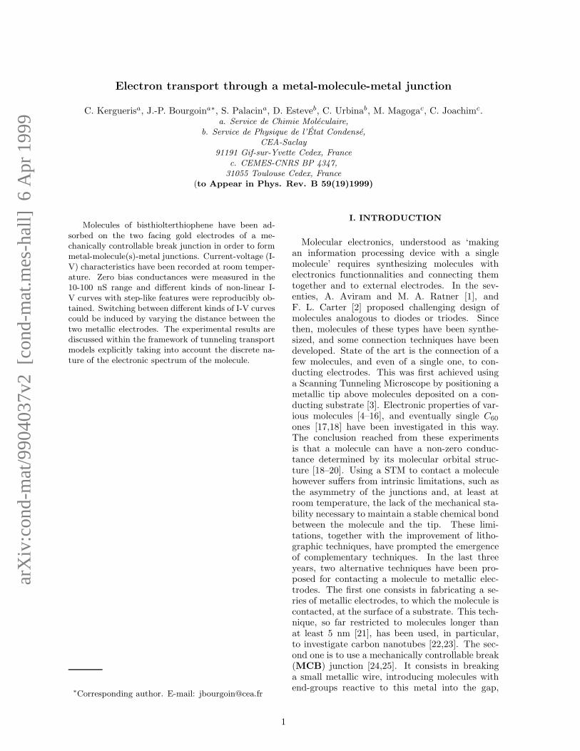
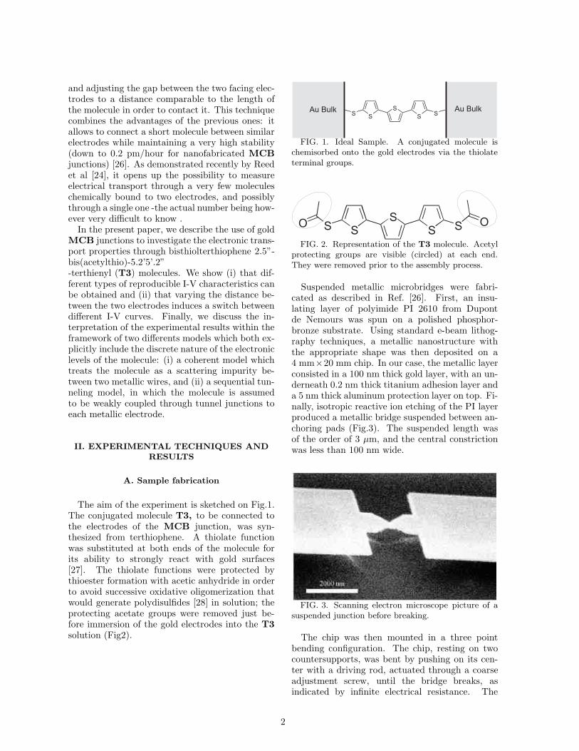
The aim of the experiment is sketched on Fig.1.The conjugated molecule T3, to be connected tothe electrodes of the MCB junction, was syn-thesized from terthiophene. A thiolate functionwas substituted at both ends of the molecule forits ability to strongly react with gold surfaces[27]. The thiolate functions were protected bythioester formation with acetic anhydride in orderto avoid successive oxidative oligomerization thatwould generate polydisulfides [28] in solution; theprotecting acetate groups were removed just be-fore immersion of the gold electrodes into the T3solution (Fig2).
SS
SS SA u B u l k A u B u l k
FIG. 1. Ideal Sample. A conjugated molecule ischemisorbed onto the gold electrodes via the thiolateterminal groups.
SS
SS S OOFIG. 2. Representation of the T3 molecule. Acetyl
protecting groups are visible (circled) at each end.They were removed prior to the assembly process.
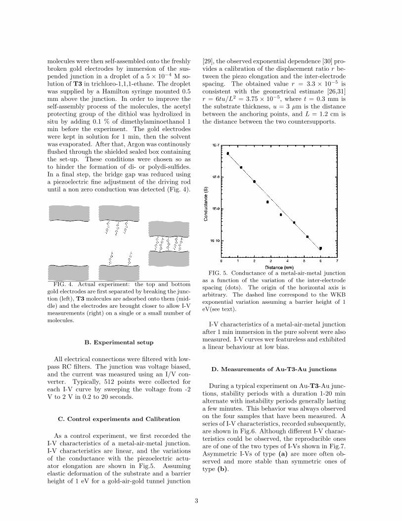
Suspended metallic microbridges were fabri-cated as described in Ref. [26]. First, an insu-lating layer of polyimide PI 2610 from Dupontde Nemours was spun on a polished phosphor-bronze substrate. Using standard e-beam lithog-raphy techniques, a metallic nanostructure withthe appropriate shape was then deposited on a4 mm×20 mm chip. In our case, the metallic layerconsisted in a 100 nm thick gold layer, with an un-derneath 0.2 nm thick titanium adhesion layer anda 5 nm thick aluminum protection layer on top. Fi-nally, isotropic reactive ion etching of the PI layerproduced a metallic bridge suspended between an-choring pads (Fig.3). The suspended length wasof the order of 3 µm, and the central constrictionwas less than 100 nm wide.
FIG. 3. Scanning electron microscope picture of asuspended junction before breaking.
The chip was then mounted in a three pointbending configuration. The chip, resting on twocountersupports, was bent by pushing on its cen-ter with a driving rod, actuated through a coarseadjustment screw, until the bridge breaks, asindicated by infinite electrical resistance. The
2
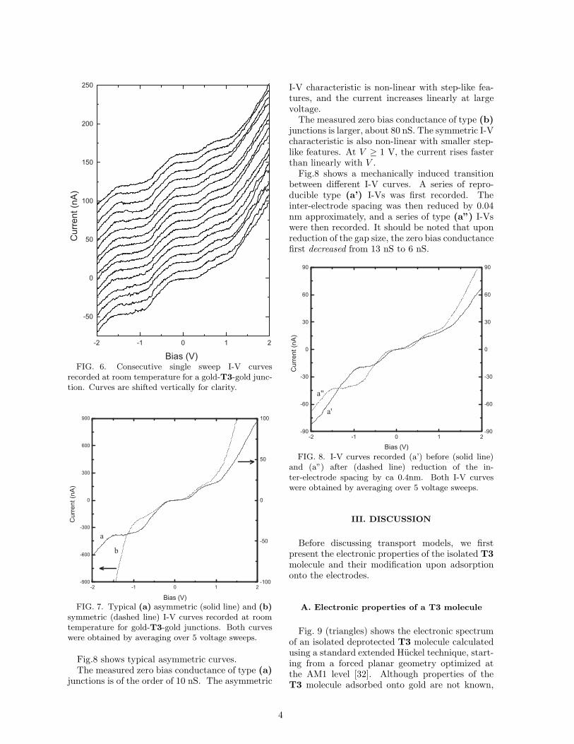
molecules were then self-assembled onto the freshlybroken gold electrodes by immersion of the sus-pended junction in a droplet of a 5 × 10⁻⁴ M so-lution of T3 in trichloro-1,1,1-ethane. The dropletwas supplied by a Hamilton syringe mounted 0.5mm above the junction. In order to improve theself-assembly process of the molecules, the acetylprotecting group of the dithiol was hydrolized insitu by adding 0.1 % of dimethylaminoethanol 1min before the experiment. The gold electrodeswere kept in solution for 1 min, then the solventwas evaporated. After that, Argon was continouslyflushed through the shielded sealed box containingthe set-up. These conditions were chosen so asto hinder the formation of di- or polydi-sulfides.In a final step, the bridge gap was reduced usinga piezoelectric fine adjustment of the driving roduntil a non zero conduction was detected (Fig. 4).
FIG. 4. Actual experiment: the top and bottomgold electrodes are first separated by breaking the junc-tion (left), T3 molecules are adsorbed onto them (mid-dle) and the electrodes are brought closer to allow I-Vmeasurements (right) on a single or a small number ofmolecules.
B. Experimental setup
All electrical connections were filtered with low-pass RC filters. The junction was voltage biased,and the current was measured using an I/V con-verter. Typically, 512 points were collected foreach I-V curve by sweeping the voltage from -2V to 2 V in 0.2 to 20 seconds.
C. Control experiments and Calibration
As a control experiment, we first recorded theI-V characteristics of a metal-air-metal junction.I-V characteristics are linear, and the variationsof the conductance with the piezoelectric actu-ator elongation are shown in Fig.5. Assumingelastic deformation of the substrate and a barrierheight of 1 eV for a gold-air-gold tunnel junction
[29], the observed exponential dependence [30] pro-vides a calibration of the displacement ratio r be-tween the piezo elongation and the inter-electrodespacing. The obtained value r = 3.3 × 10⁻⁵ isconsistent with the geometrical estimate [26,31]r = 6tu/L2 = 3.75 × 10⁻⁵, where t = 0.3 mm isthe substrate thickness, u = 3 µm is the distancebetween the anchoring points, and L = 1.2 cm isthe distance between the two countersupports.
FIG. 5. Conductance of a metal-air-metal junctionas a function of the variation of the inter-electrodespacing (dots). The origin of the horizontal axis isarbitrary. The dashed line correspond to the WKBexponential variation assuming a barrier height of 1eV(see text).
I-V characteristics of a metal-air-metal junctionafter 1 min immersion in the pure solvent were alsomeasured. I-V curves wer featureless and exhibiteda linear behaviour at low bias.
D. Measurements of Au-T3-Au junctions
During a typical experiment on Au-T3-Au junc-tions, stability periods with a duration 1-20 minalternate with instability periods generally lastinga few minutes. This behavior was always observedon the four samples that have been measured. Aseries of I-V characteristics, recorded subsequently,are shown in Fig.6. Although different I-V charac-teristics could be observed, the reproducible onesare of one of the two types of I-Vs shown in Fig.7.Asymmetric I-Vs of type (a) are more often ob-served and more stable than symmetric ones oftype (b).
3
- 2 - 1 0 1 2
- 5 0
0
5 0
1 0 0
1 5 0
2 0 0
2 5 0Cu
rrent
(nA)
B i a s ( V )FIG. 6. Consecutive single sweep I-V curves
recorded at room temperature for a gold-T3-gold junc-tion. Curves are shifted vertically for clarity.
- 2 - 1 0 1 2- 9 0 0
- 6 0 0
- 3 0 0
0
3 0 0
6 0 0
9 0 0
Curre
nt (nA
)
B i a s ( V )- 1 0 0
- 5 0
0
5 0
1 0 0
ab
FIG. 7. Typical (a) asymmetric (solid line) and (b)symmetric (dashed line) I-V curves recorded at roomtemperature for gold-T3-gold junctions. Both curveswere obtained by averaging over 5 voltage sweeps.
Fig.8 shows typical asymmetric curves.The measured zero bias conductance of type (a)
junctions is of the order of 10 nS. The asymmetric
I-V characteristic is non-linear with step-like fea-tures, and the current increases linearly at largevoltage.
The measured zero bias conductance of type (b)junctions is larger, about 80 nS. The symmetric I-Vcharacteristic is also non-linear with smaller step-like features. At V ≥ 1 V, the current rises fasterthan linearly with V .
Fig.8 shows a mechanically induced transitionbetween different I-V curves. A series of repro-ducible type (a’) I-Vs was first recorded. Theinter-electrode spacing was then reduced by 0.04nm approximately, and a series of type (a”) I-Vswere then recorded. It should be noted that uponreduction of the gap size, the zero bias conductancefirst decreased from 13 nS to 6 nS.
- 2 - 1 0 1 2- 9 0
- 6 0
- 3 0
0
3 0
6 0
9 0
- 9 0
- 6 0
- 3 0
0
3 0
6 0
9 0
Curre
nt (nA
)
B i a s ( V )
a "
a '
FIG. 8. I-V curves recorded (a’) before (solid line)and (a”) after (dashed line) reduction of the in-ter-electrode spacing by ca 0.4nm. Both I-V curveswere obtained by averaging over 5 voltage sweeps.
III. DISCUSSION
Before discussing transport models, we firstpresent the electronic properties of the isolated T3molecule and their modification upon adsorptiononto the electrodes.
A. Electronic properties of a T3 molecule
Fig. 9 (triangles) shows the electronic spectrumof an isolated deprotected T3 molecule calculatedusing a standard extended Huckel technique, start-ing from a forced planar geometry optimized atthe AM1 level [32]. Although properties of theT3 molecule adsorbed onto gold are not known,
4
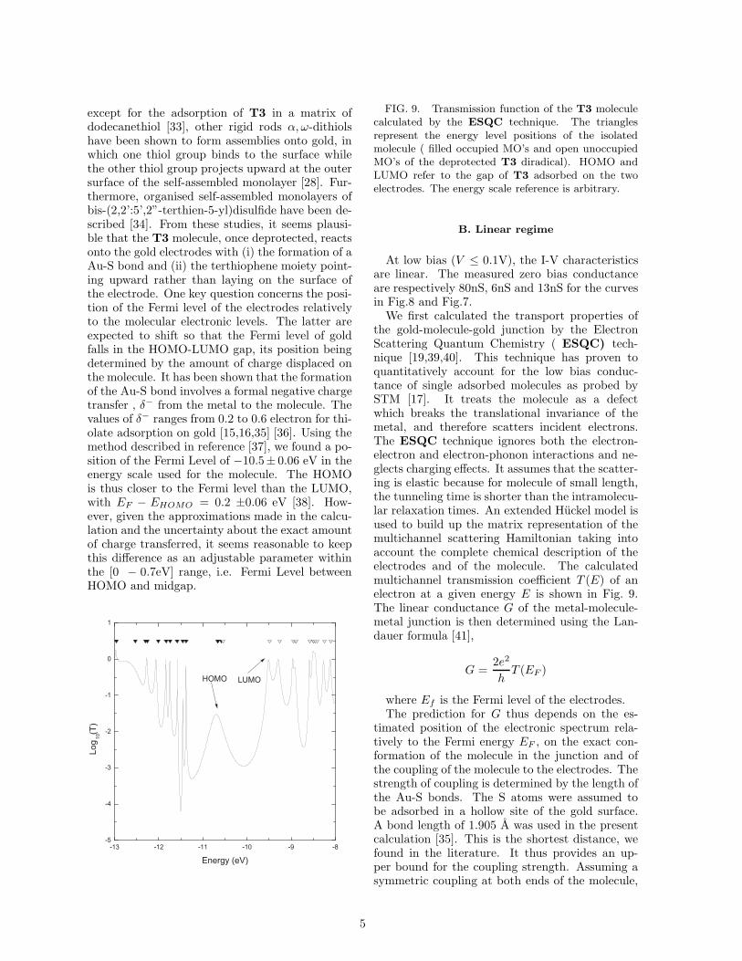
except for the adsorption of T3 in a matrix ofdodecanethiol [33], other rigid rods α, ω-dithiolshave been shown to form assemblies onto gold, inwhich one thiol group binds to the surface whilethe other thiol group projects upward at the outersurface of the self-assembled monolayer [28]. Fur-thermore, organised self-assembled monolayers ofbis-(2,2’:5’,2”-terthien-5-yl)disulfide have been de-scribed [34]. From these studies, it seems plausi-ble that the T3 molecule, once deprotected, reactsonto the gold electrodes with (i) the formation of aAu-S bond and (ii) the terthiophene moiety point-ing upward rather than laying on the surface ofthe electrode. One key question concerns the posi-tion of the Fermi level of the electrodes relativelyto the molecular electronic levels. The latter areexpected to shift so that the Fermi level of goldfalls in the HOMO-LUMO gap, its position beingdetermined by the amount of charge displaced onthe molecule. It has been shown that the formationof the Au-S bond involves a formal negative chargetransfer , δ− from the metal to the molecule. Thevalues of δ− ranges from 0.2 to 0.6 electron for thi-olate adsorption on gold [15,16,35] [36]. Using themethod described in reference [37], we found a po-sition of the Fermi Level of −10.5± 0.06 eV in theenergy scale used for the molecule. The HOMOis thus closer to the Fermi level than the LUMO,with EF − EHOMO = 0.2 ±0.06 eV [38]. How-ever, given the approximations made in the calcu-lation and the uncertainty about the exact amountof charge transferred, it seems reasonable to keepthis difference as an adjustable parameter withinthe [0 − 0.7eV] range, i.e. Fermi Level betweenHOMO and midgap.
- 1 3 - 1 2 - 1 1 - 1 0 - 9 - 8- 5
- 4
- 3
- 2
- 1
0
1
L U M OH O M O
Log 1
0(T)
E n e r g y ( e V )
FIG. 9. Transmission function of the T3 moleculecalculated by the ESQC technique. The trianglesrepresent the energy level positions of the isolatedmolecule ( filled occupied MO’s and open unoccupiedMO’s of the deprotected T3 diradical). HOMO andLUMO refer to the gap of T3 adsorbed on the twoelectrodes. The energy scale reference is arbitrary.
B. Linear regime
At low bias (V ≤ 0.1V), the I-V characteristicsare linear. The measured zero bias conductanceare respectively 80nS, 6nS and 13nS for the curvesin Fig.8 and Fig.7.
We first calculated the transport properties ofthe gold-molecule-gold junction by the ElectronScattering Quantum Chemistry ( ESQC) tech-nique [19,39,40]. This technique has proven toquantitatively account for the low bias conduc-tance of single adsorbed molecules as probed bySTM [17]. It treats the molecule as a defectwhich breaks the translational invariance of themetal, and therefore scatters incident electrons.The ESQC technique ignores both the electron-electron and electron-phonon interactions and ne-glects charging effects. It assumes that the scatter-ing is elastic because for molecule of small length,the tunneling time is shorter than the intramolecu-lar relaxation times. An extended Huckel model isused to build up the matrix representation of themultichannel scattering Hamiltonian taking intoaccount the complete chemical description of theelectrodes and of the molecule. The calculatedmultichannel transmission coefficient T (E) of anelectron at a given energy E is shown in Fig. 9.The linear conductance G of the metal-molecule-metal junction is then determined using the Lan-dauer formula [41],
G =2e2
hT (EF )
where Ef is the Fermi level of the electrodes.The prediction for G thus depends on the es-
timated position of the electronic spectrum rela-tively to the Fermi energy EF , on the exact con-formation of the molecule in the junction and ofthe coupling of the molecule to the electrodes. Thestrength of coupling is determined by the length ofthe Au-S bonds. The S atoms were assumed tobe adsorbed in a hollow site of the gold surface.A bond length of 1.905 A was used in the presentcalculation [35]. This is the shortest distance, wefound in the literature. It thus provides an up-per bound for the coupling strength. Assuming asymmetric coupling at both ends of the molecule,
5
the calculated conductances for EF − EHOMO =0.6(midgap), 0.2 and 0 eV are 87, 585, 2306 nS, re-spectively. Although the order of magnitude ofthese values is comparable with the measured oneG ≃80 nS for type (b) junctions [42], the discrep-ancy indicates that the coupling of the molecule tothe electrodes is smaller than estimated. This find-ing can be compared with the results published re-cently by Emberly and Kirczenow [43]. In that pa-per, it is shown that the experimental conductanceof gold-benzene di -thiol-gold junctions, reportedin ref. [24] can be accounted for by a transportmodel based on the Landauer formalism providedthat artificially large bond lengths (i.e. small cou-plings) are used. In our case the discrepancy be-tween theory and experience seems less importantbut could also be reduced using longer Au-S bonds:for example G0=87nS at midgap for Au-S=1.905Areduces to G0=20nS at midgap for Au-S=3A.
C. Non linear regime
We now discuss the step-like features found inthe I-V characteristics at large bias voltage andtheir possible interpretations.
At first, we can rule out the simplified Coulombblockade model put forward by Reed et al to ac-count for their experimental observations in a sim-ilar experiment with benzene dithiolate [24]. In-deed, this model, which considers the molecule asa usual metallic island forming a small capacitorwith each electrode, predicts a series of steps whichare not observed.
Consequently, we attribute the steps to the dis-creteness of the molecular levels [44]. We presentand discuss below two models which both involvethe discrete electronic levels of the molecule explic-itly. The first one is a coherent tunneling modelderived from the ESQC technique, whereas thesecond is a sequential tunneling model. Basically,they differ by the fact that the electron resides (se-quential tunneling) or not (coherent tunneling) onthe molecule during the transfer.
Given the symmetry of the molecule, symmet-ric I-V characteristics are expected in the case ofsymmetric couplings. Thus type (b) characteris-tics only will be analyzed below.
1. Coherent tunneling model
The coherent tunneling model is based on anextension of the ESQC technique outlined above.It supposes that the coupling to the electrodes isstrong, in other terms that the tunneling time of
an electron through the molecule is much smallerthan the intramolecular vibronic relaxation time:i.e. the molecule is not charged by the tunnelingprocess, the electron having no time to be com-pletely relocalized in the molecule after the initialtunneling step at the metal -molecule electroniccontact. The current is calculated using [45]:
I(V ) =e2
πh
∫ +∞
−∞
T (E, V ) (f (E − µ1) − f (E − µ2)) dE
(1)
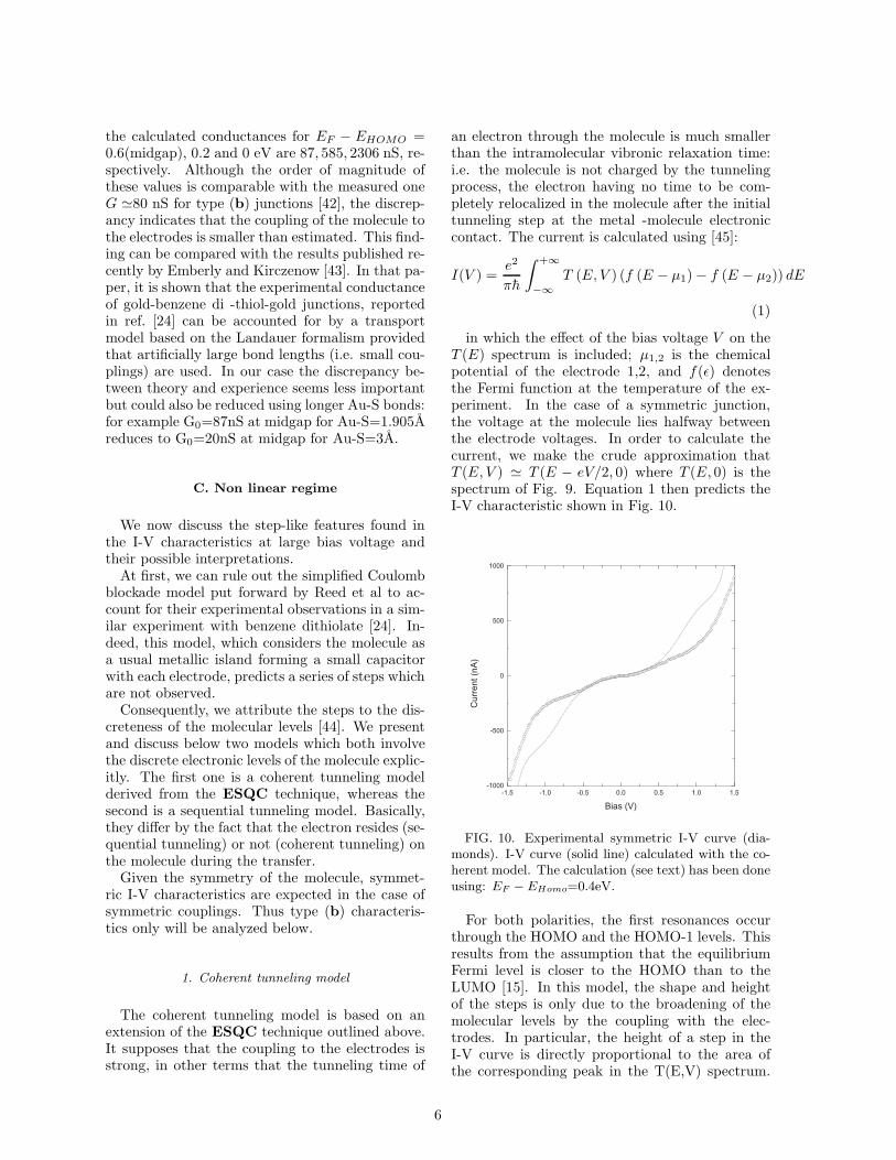
in which the effect of the bias voltage V on theT (E) spectrum is included; µ1,2 is the chemicalpotential of the electrode 1,2, and f(ǫ) denotesthe Fermi function at the temperature of the ex-periment. In the case of a symmetric junction,the voltage at the molecule lies halfway betweenthe electrode voltages. In order to calculate thecurrent, we make the crude approximation thatT (E, V ) ≃ T (E − eV/2, 0) where T (E, 0) is thespectrum of Fig. 9. Equation 1 then predicts theI-V characteristic shown in Fig. 10.
- 1 . 5 - 1 . 0 - 0 . 5 0 . 0 0 . 5 1 . 0 1 . 5- 1 0 0 0
- 5 0 0
0
5 0 0
1 0 0 0
Curre
nt (nA
)
B i a s ( V )
FIG. 10. Experimental symmetric I-V curve (dia-monds). I-V curve (solid line) calculated with the co-herent model. The calculation (see text) has been doneusing: EF − EHomo=0.4eV.
For both polarities, the first resonances occurthrough the HOMO and the HOMO-1 levels. Thisresults from the assumption that the equilibriumFermi level is closer to the HOMO than to theLUMO [15]. In this model, the shape and heightof the steps is only due to the broadening of themolecular levels by the coupling with the elec-trodes. In particular, the height of a step in theI-V curve is directly proportional to the area ofthe corresponding peak in the T(E,V) spectrum.
6
The experimental curve is well reproduced for the[−0.5V, 0.5V ] range. Outside of this range, thecalculated current is higher than the experimen-tal one. It should be noted that the only ad-justable parameter used in the calculation is theposition of the Fermi level. Here we have takenEF − EHOMO = 0.4 eV. In this calculation, themagnitude of the current depends on the followingpoints: i) the overlap between the orbitals of theouter Au atoms and of the sulfur atoms; ii) the lo-calisation of the molecular orbital and its symme-try, iii) perfect symmetry between the two contacts[46]. The applied voltage is expected , especially athigh bias, to affect points ii) and iii), both of whichshould tend to decrease the calculated current andthus reduce the discrepancy.
2. Sequential tunneling model
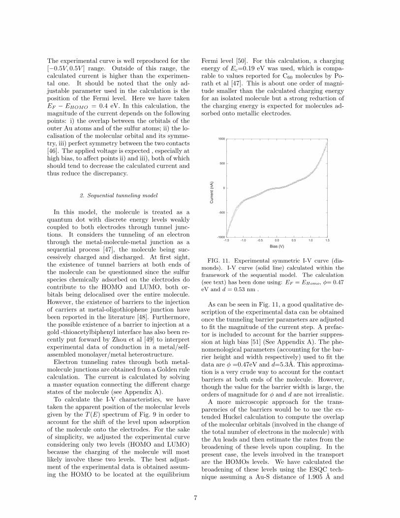
In this model, the molecule is treated as aquantum dot with discrete energy levels weaklycoupled to both electrodes through tunnel junc-tions. It considers the tunneling of an electronthrough the metal-molecule-metal junction as asequential process [47], the molecule being suc-cessively charged and discharged. At first sight,the existence of tunnel barriers at both ends ofthe molecule can be questionned since the sulfurspecies chemically adsorbed on the electrodes docontribute to the HOMO and LUMO, both or-bitals being delocalised over the entire molecule.However, the existence of barriers to the injectionof carriers at metal-oligothiophene junction havebeen reported in the literature [48]. Furthermore,the possible existence of a barrier to injection at agold -thioacetylbiphenyl interface has also been re-cently put forward by Zhou et al [49] to interpretexperimental data of conduction in a metal/self-assembled monolayer/metal heterostructure.
Electron tunneling rates through both metal-molecule junctions are obtained from a Golden rulecalculation. The current is calculated by solvinga master equation connecting the different chargestates of the molecule (see Appendix A).
To calculate the I-V characteristics, we havetaken the apparent position of the molecular levelsgiven by the T (E) spectrum of Fig. 9 in order toaccount for the shift of the level upon adsorptionof the molecule onto the electrodes. For the sakeof simplicity, we adjusted the experimental curveconsidering only two levels (HOMO and LUMO)because the charging of the molecule will mostlikely involve these two levels. The best adjust-ment of the experimental data is obtained assum-ing the HOMO to be located at the equilibrium
Fermi level [50]. For this calculation, a chargingenergy of Ec=0.19 eV was used, which is compa-rable to values reported for C60 molecules by Po-rath et al [47]. This is about one order of magni-tude smaller than the calculated charging energyfor an isolated molecule but a strong reduction ofthe charging energy is expected for molecules ad-sorbed onto metallic electrodes.
- 1 . 5 - 1 . 0 - 0 . 5 0 . 0 0 . 5 1 . 0 1 . 5- 1 0 0 0
- 5 0 0
0
5 0 0
1 0 0 0
Curre
nt (nA
)
B i a s ( V )
FIG. 11. Experimental symmetric I-V curve (dia-monds). I-V curve (solid line) calculated within theframework of the sequential model. The calculation(see text) has been done using: EF = EHomo, φ= 0.47eV and d = 0.53 nm .
As can be seen in Fig. 11, a good qualitative de-scription of the experimental data can be obtainedonce the tunneling barrier parameters are adjustedto fit the magnitude of the current step. A prefac-tor is included to account for the barrier suppres-sion at high bias [51] (See Appendix A). The phe-nomenological parameters (accounting for the bar-rier height and width respectively) used to fit thedata are φ =0.47eV and d=5.3A. This approxima-tion is a very crude way to account for the contactbarriers at both ends of the molecule. However,though the value for the barrier width is large, theorders of magnitude for φ and d are not irrealistic.
A more microscopic approach for the trans-parencies of the barriers would be to use the ex-tended Huckel calculation to compute the overlapof the molecular orbitals (involved in the change ofthe total number of electrons in the molecule) withthe Au leads and then estimate the rates from thebroadening of these levels upon coupling. In thepresent case, the levels involved in the transportare the HOMOs levels. We have calculated thebroadening of these levels using the ESQC tech-nique assuming a Au-S distance of 1.905 A and
7
considering each molecular orbital separately toavoid any interference effect between orbitals (suchan interference effect takes place, for example, be-tween the HOMO and HOMO-1 orbitals in theT(E) spectrum in Fig. 9 and explains the nonunity value of the corresponding peak). We founda width at half maximum of 0.4eV correspondingto a transfer rate of about 3 1014 Hz. This is toohigh when compared to the experimental rates ofthe order of 1012 Hz. To get the right order ofmagnitude artificially large Au-S distances haveto be used (typically 6 A). This shows that thecalculation of the coupling strength based on theextended Huckel model likely leads to an overes-timated value as already pointed out in the linearregime subsection above. At present, this micro-scopic approach unfortunately cannot be used toestimate the barrier suppression at high bias, be-cause the extended Huckel calculation do not takeinto account the modification of the orbitals underbias.
3. Discussion
To summarize, both the coherent model at lowbias and the sequential model at large bias givequalitative fits of the experimental I-V curves.This provides support to the hypothesis that thestep like features in the I-V curve indeed originatein the discreteness of the molecular levels. How-ever a quantitative fit of the data has not beenachieved. This may be explained as follows. First,the effect of the applied bias on the relative posi-tion of the resonances in the T (E) spectrum is ne-glected, since we consider that the bias effect is toshift T (E) as a whole. Although the electric fieldsinvolved in the experiments are always lower than1× 109 V/m, the position of the levels is expectedto be modified [52]. Preliminary calculation usingthe DFT formalism have shown that the HOMO-LUMO gap of the bisthiol-bisthiophene molecule isindeed reduced under an electric field [53], and thiseffect is expected to take place also with T3. An-other effect of the field is to modify the coupling be-tween the molecule and the electrodes. This shouldshow up in the T (E, V ) spectrum as a modificationof the width of the peaks and consequently in theI(V) as a modification of the height of the steps.
Second, in the calculation, the molecule is as-sumed to be in the vacuum. In reality, given theexperimental conditions, the molecule can be as-sumed to be surrounded by Argon and probably afew solvent molecules. We have not taken this envi-ronment into account in our calculations. Smooth-ing of the theoretical I-Vs of both models is ex-
pected due to this polarizable surrounding.Additional experimental results and theoretical
calculations are clearly needed to help deciding be-tween sequential and coherent tunneling or a com-bination of both. This includes : (i) measure-ments in a better controlled environment (UHV),and at low temperature to determine the originof the broadening of the steps in the I-V curve,(ii) calculation of the potential profile along themolecule in order to determine wether tunnelingbarriers are present at the end of the molecule ornot and (iii) estimation of the tunneling times in-volved in the processes. Furthermore, it should benoted that two proposed model indeed correspondto extreme cases. In the coherent one, the chargingeffect is neglected, whereas in the sequential one,the quantum coherence is neglected. In our quali-tative fits, it turns out that the order of magnitudeof the molecular level broadening (coherent model)and charging energy(sequential model) are compa-rable. Thus a proper model will very likely haveto take into account both coherent and sequentialtransport.
Compared to the symmetric case, the interpreta-tion of the asymmetric I(V) curves of Fig. 7 (curvea) and Fig 8 is more complicated because we can nolonger assume that the coupling to the electrodesis symmetric at both ends of the molecule. First,these data likely correspond to the case where atleast one end of the molecule is less coupled tothe electrode than in the case of the symmetriccurve since i) the zero bias conductance is smallerthan in the symmetric case and ii) the high biasbehaviour of the current is linear-like rather thanexponential-like. Second, the effect of mechani-cally pushing on the molecule(s) induces a changebetween two different stable curves. Such an effecthas been used recently at low bias to realise an elec-tromechanical amplifier based on a C60 molecule[54]. In the present case, two explanations of theobservations can be put forward: either the cou-pling of the molecule to the electrodes is changedby the mechanical action, or a change in the con-formation of the molecule was induced.
IV. CONCLUSION
In this paper, we have investigated the trans-port properties of molecules of 2,5”-bis(acetylthio)-5,2’,5’,2”-terthienyl self-assembled in the ad-justable gap of a metallic break junction. We haveobserved that the I-V characteristics recorded atroom temperature are not always symmetric withrespect to the polarity of the applied bias and showtwo different regimes: a linear regime at low bias
8
V < 0.1 V and a highly non-linear regime withstep-like features at higher voltage. The orderof magnitude of the measured zero bias conduc-tance is comparable to the theoretical calculationmade with the ESQC technique assuming a singlemolecule in the gap of the break junction. Thisindicates that these experiments likely involve avery few molecules. We have obtained qualitativefits of the symmetric I-V curves using two differ-ent models of transport, a coherent one for the lowbias range and a sequential one for the high biasrange, both of which explicitly involve the elec-tronic structure of the molecule. Finally, we haveshown that the mechanical action of decreasing thegap size by 0.04 nm induces a strong modificationof the I-V curves.
Acknowledgments : We thank C. Bureau andM. Devoret for enlightening discussions, C. Blondand T. Risler for their contribution to the sequen-tial model calculations, O. Araspin for his helpwith the e-beam lithography.
APPENDIX A: THE SEQUENTIAL MODEL
1. Description of the system
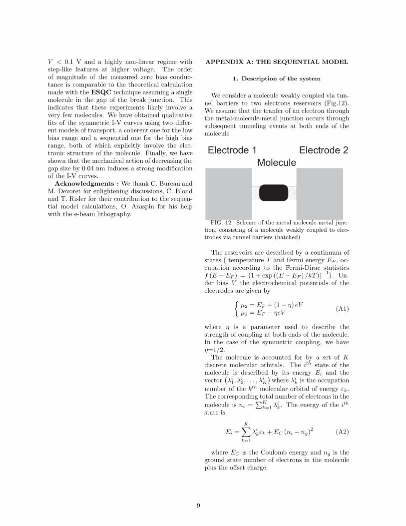
We consider a molecule weakly coupled via tun-nel barriers to two electrons reservoirs (Fig.12).We assume that the tranfer of an electron throughthe metal-molecule-metal junction occurs throughsubsequent tunneling events at both ends of themolecule
E l e c t r o d e 1 E l e c t r o d e 2M o l e c u l e
FIG. 12. Scheme of the metal-molecule-metal junc-tion, consisting of a molecule weakly coupled to elec-trodes via tunnel barriers (hatched)
The reservoirs are described by a continuum ofstates ( temperature T and Fermi energy EF , oc-cupation according to the Fermi-Dirac statisticsf (E − EF ) = (1 + exp ((E − EF ) /kT ))
−1). Un-
der bias V the electrochemical potentials of theelectrodes are given by
{µ2 = EF + (1 − η) eVµ1 = EF − ηeV
(A1)
where η is a parameter used to describe thestrength of coupling at both ends of the molecule.In the case of the symmetric coupling, we haveη=1/2.
The molecule is accounted for by a set of Kdiscrete molecular orbitals. The ith state of themolecule is described by its energy Ei and thevector
(λi
1, λi2, . . . , λ
iK
)where λi
k is the occupation
number of the kth molecular orbital of energy εk.The corresponding total number of electrons in the
molecule is ni =∑K
k=1λi
k. The energy of the ith
state is
Ei =K∑
k=1
λikεk + EC (ni − ng)
2 (A2)
where EC is the Coulomb energy and ng is theground state number of electrons in the moleculeplus the offset charge.
9
2. Calculation of the transfer rates
The rate of transfer of electrons through the tun-nel barriers are calculated by application of theFermi golden rule assuming that the tunneling pro-cesses are elastic.
The rate Γk+
i,j for the process connecting the ith
state and jth state through the transfer of one elec-tron from electrode k onto the molecule is given by.
Γk+
i,j =2π
h|Ti,j|
2ρkf (Ej − Ei)
where Tij is the tunnel matrix element couplingthe states i and j, and ρk is the density of statesof the electrode k, assumed constant around theFermi level.
We define in the same way Γk−i,j connecting the
states i and j by transferring one electron from themolecule onto electrode k.
Γk−i,j =
2π
h|Ti,j |
2ρk (1 − f (Ei − Ej))
Assuming that the tunneling barriers have aheight φ and a width d, we apply a WKB typeapproximation for the tunneling matrix element
|Ti,j (Vb)|2 α exp(−2
√2m(φ − eVb)
hd)
where Vb is the voltage drop across a tunnel junc-tion.
3. Calculation of the current
The matrix Γ connecting the different states ofthe molecule is [55]
Γ = Γ1+ + Γ1− + Γ2+ + Γ2− (A3)
We introduce the vector P , which ith compo-nent is the probability of having the molecule instate i. The evolution of the system is then de-scribed by
d
dtPi =
∑
j
(ΓjiPj − ΓijPi) (A4)
defining M by Mij=Γji i 6= j and Mii=−∑
j Γij
equation A4 becomes,
d
dtP = MP
We look for a stationary solution P assumingthat a permanent regime rapidly sets in
P = kerM
The current is finally obtained by calculating thenet number of electrons transferred from right toleft through either junction:
I = e∑
i,j
Pj
(Γ1−
ji − Γ1+
ji
)= −e
∑
i,j
Pj
(Γ2−
ji − Γ2+
ji
)
(A5)
[1] A. Aviram and M. A. Ratner, Chem. Phys.Lett. 29, 277 (1974).
[2] F. L. Carter 2nd Intl Symp. Molecular Elec-tronic Devices (M. Dekker, New York) 149 (1982).
[3] A. Aviram, C. Joachim, and M. Pomerantz,
Chem. Phys. Lett. 146, 490 (1988).[4] G. Lambin, M. H. Delvaux, A. Calderone, R.
Lazzaroni, J. L. Bredas, T. C. Clarke and J.
P. Rabe, Mol. Cryst. Liq. Cryst. 235, 75 (1993).[5] D. M. Cyr, B. Venkataraman, G. W. Flynn,
A. Black and G. M. Whitesides, J. Phys.Chem. 100, 13747 (1996).
[6] W. Han, E. N. Durantini, T. A. Moore, A. L.
Moore, D. Gust, P. Rez, G. Leatherman, G.
R. Seely, N. Tao and S. M. Lindsay, J. Phys.Chem. B 101, 10719 (1997).
[7] H. Nejoh Nature 353, 640 (1991).[8] W. Mizutani, M. Shigeno, K. Kajimura and
M. Ono, Ultramicroscopy 42-44, 236 (1991).[9] D. Porath and O. Millo, J. Appl. Phys. 81,
2241 (1997).[10] B. Michel, G. Travaglini, H. Rohrer, C.
Joachim and M. Amrein, Z. Phys. B 76, 99(1989).
[11] X. Lu, K. W. Hipps, X. D. Wang and U.
Marzur, J. Am. Chem. Soc. 118, 7197 (1996).[12] L. A. Bumm, J. J. Arnold, M. T. Cygan, T.
D. Dunbar, T. P. Burgin, L. Jones II, D. L.
Allara, J. M. Tour, P. S. Weiss Science 271,1705 (1996).
[13] C. Dekker, S. J. Tans, B. Oberndorff, R.
Meyer and L. C. Venema, Synth. Met. 84, 853(1997).
[14] R. M. Metzger, B. Chen, U. Hopfner, M. V.
Lakshmikantham, D. Vuillaume, T. Kawai,
X. Wu, H. Tachibana, T. V. Hughes, H. Saku-
rai, J. W. Baldwin, C. Hosch, M. P. Cava,
L. Brehmer and G. L. Ashwell, J. Am. Chem.Soc. 119, 10455 (1997).
[15] S. Datta, W. Tian, S. Hong, R. Reifen-
berger, J. I. Henderson and C. P. Kubiak,
Phys. Rev. Lett. 79, 2530 (1997).
10
[16] A. Dhirani, P.-H. Lin, P. Guyot-Sionnest, R.
W. Zehner and L. R. Sita J. Chem. Phys. 106,5249 (1997).
[17] C. Joachim, J. K. Gimzewski, R. R. Schlitter
and C. Chavy, Phys. Rev. Lett. 74, 2102 (1995).[18] C. Joachim, and J. K. Gimzewski, Europhys.
Lett. 30, 409 (1995).[19] P. Sautet and C. Joachim, Chem. Phys. Lett.
v185, 23 (1989).[20] V. Mujica, M. Kemp, A. Roitberg and M.
Ratner, J. Chem. Phys. 104, 7296 (1996).[21] V. Rousset, C. Joachim, B. Rousset and N.
Fabre J. Phys.III, 5, 1985 (1995).[22] S. J. Tans, M. H. Devoret, H. Dai, A. Thess,
R. E. Smalley, L. J. Geerligs and C. Dekker
Nature. 386, 474 (1997).[23] T. W. Ebbesen, H. J. Lezec, H. Hiura, J. W.
Bennett, H. F. Ghaemi and T. Thio Nature.382, 54 (1996).
[24] M. A. Reed et al, Science 278, 252 (1997).[25] C. J. Muller, B.J. Vleeming, M. A. Reed,
J.J.S. Lambda, R. Hara, L JonesII, and J.M.
Tour Nanotechnology 7, 409 (1996).[26] J. M. van Ruitenbeek, A. Alvarez, I.
Pineyro, C. Grahmann, P. Joyez, M. H. De-
voret, D. Esteve and C. Urbina, Rev. Sci. In-strum. 67, 108 (1995).
[27] Ulman, Ultrathin organic films. (Academic press,San Diego, 1991).
[28] J. M. Tour et al, J. Am. Chem. Soc. 117, 9529(1995).
[29] C. Lebreton Ph. D. Thesis, Paris 6 (1996).[30] J. G. Simmons J. Appl. Phys. 34, 1793 (1963).[31] R. J. P. Keijsers, O. I. Shklyarevskii, J. G.
H. Hermsen and H. van Kempen, Rev. Sci. In-strum. 67, 2863 (1996).
[32] For this calculation we used the following 3s, 3pand 3d parameters for the S atoms (S. Alvarez,Extended Huckel parameters, Barcelona University(1989)): Hii = −20 eV, ξi1 = 2.122, Hii = −11.1eV, ξi1 = 1.827, Hii = −8 eV, ξi1 = 1.5. StandardHoffmann parameters were used for the C and Hatoms.
[33] C. Kergueris, J. P. Bourgoin and S. Palacin,
Nanotechnology 10,8 (1999)[34] B. Liedberg, Z. Yang, I. Engquist, M. Wirde,
U. Gelius, G. Gotz, P. Bauerle, R.M. Rum-
mel, Ch. Ziegler and W. Gopel, J. Phys.Chem. B 101, 5951 (1997).
[35] H. Sellers, A. Ulman, Y. Shnidman and J. E.
Eilers, J. Am. Chem. Soc., 115, 9389 (1993).[36] The right value to use with the T3 molecule is
not available in the litterature. A self-consistentapproach within the DFT formalism is expectedto provide a reliable value.C. Bureau, C. Ker-
gueris, and J. P. Bourgoin manuscript inpreparation.
[37] W. Tian, S. Datta, S. Hong, R. Reifen-
berger, J. I. Henderson and C. P. Kubiak,
J Chem. Phys 109, 2874 (1998).[38] The use of a shift in energy of the molecular levels
with regard to the Fermi level of the electrodes is aformal convenient way to account for a more com-plex reality. Indeed, the adjustment of the molec-ular levels to the electrodes levels should be ac-counted for in the density of states of the metalelectrodes, a term we consider here as a constantand presently hidden in the calculation.
[39] C. Joachim and J. F. Vinuesa, Europhys. Lett.33, 635 (1996).
[40] M. Magoga and C. Joachim, Phys. Rev. B 56,4722 (1997).
[41] M. Buttiker, Y. Imry, R. Landauer and S.
Pinhas, Phys. Rev. B 31, 6207 (1985).[42] Performing the same calculation on T6, the dimer
of T3 formed by disulfide coupling, gives G= 3 nSat midgap [46]. This value is also compatible withexperimental ones. Given the experimental con-ditions we nevertheless think that the formationof T6 is unlikely. An other possibility is to con-sider T3 conformers. Twisting the central thio-phene ring from planar geometry anti-anti to pla-nar geometry syn-syn, G was found to vary in therange 1.5−73.5 nS at midgap. Since the calcu-lated energy differences between the conformersare varying less than 1.02 kCal/mol (about 2kT )at the AM1 level, a conformational interconversioncan occur even at room temperature.
[43] E.G. Emberly and G. Kirczenow in Phys. Rev.B 58, 10911(1998).
[44] Such an hypothesis was also evoked by M. Reed[24] et al.
[45] S. Datta, Electronic Transport in MesoscopicSystems (Cambridge University Press, Cambridge,1995).
[46] C. Kergueris, J. P. Bourgoin, M. Magoga,
C. Joachim and S. Palacin, manuscript inpreparation.
[47] D. Porath, Y. Levi, M. Tarabiah and O.
Millo, Phys. Rev. B 56, 1 (1997).[48] C. Ziegler, Handbook of organic conductive
molecules and polymers: Vol. 3. Conductive poly-mers: spectroscopy and physical properties. Chap.13 (H. S. Nalwa, 1997).
[49] C. Zhou, M. R. Deshpande, M. A. Reed, L.
Jones II, and J. M. Tour, Appl. Phys. Lett. 71,611 (1997).
[50] A temperature of 600 K was used in the calcula-tion to account for a possible broadening of thelevel due to the adsorption or induced by the sur-rounding.
[51] A. Korotkov, and Y. Nazarov, Physica B 173,217 (1991).
[52] R. Lazzaroni, A. Calderone, J.L. Bredas
and J.P. Rabe, J. Chem. Phys. 107, 99 (1997).[53] C. Bureau, C. Kergueris and J. P. Bourgoin,
manuscript in preparation.[54] C. Joachim and J. K. Gimzewski Chem. Phys.
11

Lett. 265, 353 (1997).[55] D. Weinmann, W. Haisler and B. Kramer,
Ann. Physik., 5, 652 (1996).
12


