Embed Size (px)
Citation preview
Electromagnetics and Antenna Technology, Chapters 1, 2, 3
Alan J. Fenn
Senior Staff MemberLincoln Laboratory
Massachusetts Institute of Technology244 Wood Street
Lexington, MA 02420
January 12, 2017
DISTRIBUTION STATEMENT PENDING
This material is based upon work supported under Air Force Contract No. FA8721-05-C-0002 and/or FA8702-15-D-0001. Any opinions, findings, conclusions or recommendations expressed in this material are those of the author(s) and do not necessarily reflect the views of the U.S. Air Force.

Contents
Preface xii
1 Electromagnetics and Antenna Theory 1
1.1 Introduction 1
1.2 Some Basics: Transmission Lines and Antennas as a Load 51.2.1 Introduction 51.2.2 Transmission line impedance 61.2.3 Smith chart theory 111.2.4 Impedance Matching Circuit Elements 141.2.5 S-parameters 211.2.6 T-Chain Scattering Matrices for Cascaded Networks 27
1.3 Electromagnetic Radiation: Maxwell’s Equations 29
1.4 Fields from Time-Varying Electric and Magnetic CurrentSources 42
1.4.1 Magnetic Vector Potential and the Scalar Green’s Function 441.4.2 Dyadic Green’s Function 50
1.5 Boundary Conditions 63
1.6 Wave Equation for Conducting Media, Propagation Parameters 65
1.7 Electromagnetic Energy Flow 71
1.8 Fields of Short Electric and Magnetic Dipoles 761.8.1 Introduction 761.8.2 Derivation of Fields for z Hertzian Dipole 77
vii

viii Electromagnetics and Antenna Technology
1.8.3 Derivation of Fields for an Arbitrarily Polarized Hertzian Dipole 801.8.4 Duality and Fields for Hertzian Loop and Dipole Antennas 83
1.9 Far-Zone Fields of Arbitrary Dipoles and Loops 841.9.1 Introduction 841.9.2 Far-Zone Fields for z Oriented Dipoles and Loops 851.9.3 Far-Zone Fields for x Oriented Dipoles and Loops 881.9.4 Far-Zone Fields for y Oriented Dipoles and Loops 891.9.5 Image Theory for Electric and Magnetic Dipole Antennas 89
1.10 Electromagnetic Wave Polarization and Receive Antennas 901.10.1 Wave Polarization Theory 901.10.2 Short Dipole Receive Characteristics 1001.10.3 Small Current Loop Receive Characteristics 1011.10.4 Ferrite-Loaded Small Current Loop Receive Characteristics 103
1.11 Bandwidth and Quality Factor 1041.11.1 Introduction 1041.11.2 Derivation of Q Factor from Input Impedance 1061.11.3 Example: Q Factor for a Dipole Antenna 1081.11.4 Example: Q Factor for a Circular Loop Antenna 112
1.12 Antenna Directivity 1151.12.1 Hertzian Dipole or Electrically Small Loop Directivity Pattern 1171.12.2 Crossed Hertzian Dipoles (Turnstile Antenna) Directivity Pattern118
1.13 Antenna Gain, Realized Gain, and Transmit Power 119
1.14 Summary 124
References 125
2 Phased Array Antennas 133
2.1 Introduction 133
2.2 Phased Array Basics 1342.2.1 Introduction 1342.2.2 Wavefront Basics 1372.2.3 Beamformer Architectures 1402.2.4 Arrays of Isotropic Antenna Elements 1492.2.5 Polarized Array Far-Zone Electromagnetic Fields 1542.2.6 Array Mutual Coupling Effects 1562.2.7 Power Density and Array Gain 161
2.3 Equivalence Principles 164

Contents ix
2.4 Reciprocity Theorem 167
2.5 Reaction Integral Equation 168
2.6 Method of Moments 169
2.7 Broadside and Endfire Linear Arrays of Hertzian Dipoles 175
2.8 Example of 2D Array Mutual Coupling Effects 176
2.9 Swept-Back Dipole Array Measurements and Simulations 1772.9.1 Introduction 1772.9.2 Dipole Element Prototypes 1822.9.3 Measured and Simulated Results 183
2.10 Rectangular Waveguide Array Example 187
2.11 Summary 190
References 191
3 Line Transformer Matching of a Dipole Antenna 201
3.1 Introduction 201
3.2 Basic Transmission Line Theory 203
3.3 Line Transformer Impedance Matching Theory 2053.3.1 Target Circle for Maximum Allowed VSWR 2073.3.2 Transformation Circle Derivation 208
3.4 Wideband V-Dipole Antenna Simulation 2103.4.1 Dipole Design and Moment Method Simulation Model 2103.4.2 Impedance Matching Procedure for the Wideband Dipole 2123.4.3 Impedance Matching Simulated Results for the Wideband Dipole213
3.5 Comparison with Measurements 219
3.6 Swept-Back Dipole Feeding a Parabolic Reflector 219
3.7 Summary 223
References 225
Note: Additional chapters will follow
1Electromagnetics and AntennaTheory
1.1 Introduction
Electromagnetics [1–14] and antenna technology [15–29] are well developedand they have numerous practical applications. Radiofrequency (RF) elec-tromagnetic waves can be produced by natural and manufactured processes.There are numerous antenna designs that can be considered for radar andcommunications applications depending on frequency band, type of platformand many other considerations to be discussed in this book. This bookprovides a detailed review of fundamental electromagnetics and antennatheory and development of practical implementations of antenna technologyincluding phased arrays [30–47]. As part of the development of antennatheory, detailed discussions of transmission lines and antennas as a loadimpedance are provided. For some of the antennas described in this book,details of impedance matching between the antenna and transmission line aregiven based on well established methods.
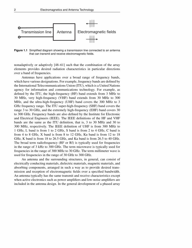
An antenna is a transducer that can convert both an incident RFelectromagnetic wave to a time-varying signal voltage (or waveform) on atransmission line and a time-varying signal voltage on a transmission line to atransmitted polarized electromagnetic wave [1–28] as depicted in Figure 1.1.An antenna can be characterized by a number of parameters includingbandwidth, impedance, scattering parameters, gain, directivity, beamwidth,polarization, and sidelobes. A phased array antenna system [30–47] consistsof two or more antenna elements that typically transmit or receive signalswith a proper timing (phase relation) and amplitude relationship betweenthe elements. Arrays operate with analog or digital beamforming either
1
2 Electromagnetics and Antenna Technology
Transmission line Antenna Electromagnetic fields
Figure 1.1 Simplified diagram showing a transmission line connected to an antennathat can transmit and receive electromagnetic fields.
nonadaptively or adaptively [48–61] such that the combination of the arrayelements provides desired radiation characteristics in particular directionsover a band of frequencies.
Antennas have applications over a broad range of frequency bands,which have various designations. For example, frequency bands are defined bythe International Telecommunications Union (ITU), which is a United Nationsagency for information and communications technology. For example, asdefined by the ITU, the high-frequency (HF) band extends from 3 MHz to30 MHz, very high-frequency (VHF) band extends from 30 MHz to 300MHz, and the ultra-high-frequency (UHF) band covers the 300 MHz to 3GHz frequency range. The ITU super-high-frequency (SHF) band covers therange 3 to 30 GHz, and the extremely high-frequency (EHF) band covers 30to 300 GHz. Frequency bands are also defined by the Institute for Electronicand Electrical Engineers (IEEE). The IEEE definitions of the HF and VHFbands are the same as the ITU definition, that is, 3 to 30 MHz and 30 to300 MHz, respectively. The IEEE definition of UHF is from 300 MHz to1 GHz, L band is from 1 to 2 GHz, S band is from 2 to 4 GHz, C band isfrom 4 to 8 GHz, X band is from 8 to 12 GHz, Ku band is from 12 to 18GHz, K band is from 18 to 26.5 GHz, and Ka band is from 26.5 to 40 GHz.The broad term radiofrequency (RF or Rf) is typically used for frequenciesin the range of 3 kHz to 300 GHz. The term microwave is typically used forfrequencies in the range of 300 MHz to 30 GHz. The term millimeter wave isused for frequencies in the range of 30 GHz to 300 GHz.
An antenna and the surrounding structures, in general, can consist ofelectrically conducting materials, dielectric materials, magnetic materials, andabsorbing components, arranged in such a way as to provide desired trans-mission and reception of electromagnetic fields over a specified bandwidth.An antenna typically has the same transmit and receive characteristics exceptwhen active electronics such as power amplifiers and low-noise amplifiers areincluded in the antenna design. In the general development of a phased array

Electromagnetics and Antenna Theory 3
antenna, the following topics often are important considerations as listed inTable 1.2.
Table 1.1Some important topics in electromagnetics and antenna technology
Antenna typesTransmission linesReflection coefficient, input impedanceImpedance matchingMaxwell’s equationsElectromagnetic simulationsMaterials (conductivity, permittivity, permeability)BandwidthPolarizationRadiation patterns, directivity, gainNear field, far fieldResonant antennasElectrically small antennasFinite, infinite arraysPeriodic, random arrays, sparse arraysLinear, planar, conformal arraysArray mutual couplingBeamformingGrating lobes, Blind spotsInterference, Low sidelobes, Adaptive nullingDirection findingSubarrays, Phase centersElectronic scanningPassive electronically scanned array (PESA)Active electronically scanned array (AESA)Transmit/Receive modulesPhase shifters, time delaysHigh-power amplifiers, low noise amplifiersArray design, fabrication, measurementsArray calibrationRadomesRadar cross-section controlField testing

4 Electromagnetics and Antenna Technology
In developing antenna technology, a number of detailed design parame-ters as well as testing methods need to be considered as listed below:
• Antenna system design and testing
– RF radiation parameters∗ Field of view, scan sector, bandwidth (in-band, out-of-
band), polarization, gain, half-power beamwidth, sidelobelevel, front-to-back ratio, null depth, reflection coefficient,noise figure, effective isotropic radiated power
– RF components∗ Antenna radiating elements∗ Beamformer: feed cables, transmission lines, connectors,
combiners, amplifiers, filters, couplers, circulators, switches,attenuators, phase shifters, time-delay units
Table 1.2Some common antenna types
Arrays (phased, broadside, endfire, lens, reflect)Biconical (symmetric, asymmetric, solid surface, wire frame)Dielectric rodDipole (linear, folded, vee, ultrawideband)Discone (solid, wire frame)Helix [axial mode (endfire), normal mode (broadside)]Horn (pyramidal, conical, corrugated)Lens (dielectric)Log periodicLong wireLoop (circular, square)Monocone (solid surface, wire frame)Monopole (wire, sleeve, top loaded, blade)Notch (flared Vivaldi, stepped)Parasitic (Yagi-Uda)Patch (circular, rectangular, triangular, microstrip, suspended)Reflectors (corner, parabolic, shaped, dual)SlotSpiral (planar: Archimedean, equiangular; conical)Subreflectors (parabolic, elliptical, hyperbola, shaped)Waveguide (open-ended: rectangular, circular)
Electromagnetics and Antenna Theory 5
– Mechanical parameters∗ Antenna volume and mass budget, antenna durability/survivability,
fabrication technique(s) and materials, ground plane andsupport structure
– Ground-based testing∗ Anechoic chamber measurements (far-field [rectangular
chamber, tapered chamber, compact range], near-field [pla-nar, cylindrical, spherical])∗ Thermal chamber, vacuum chamber measurements∗ Outdoor field testing
– Flight testing (airborne, spaceborne)∗ In-flight radiation patterns and calibration
The rest of this chapter is organized as follows. Section 1.2 reviewstransmission line theory as it relates to antennas and provides variousdefinitions for bandwidth. In Section 1.3, the generation of electromagneticradiation and Maxwell’s equations are described. Since the goal of electro-magnetic analysis often is to compute the radiation pattern of antennas, inSection 1.4, a derivation of the fields radiated by current sources is given.Boundary conditions for the relations between the field quantities at theinterface between two arbitrary media are derived in Section 1.5. Section1.6 describes the wave equation and the complex propagation constant ofelectromagnetic waves in conducting media. In Section 1.7, a derivationof the electromagnetic wave energy flow and Poynting vector is given.Section 1.8 considers the derivation of near-field and far-field expressions forHertzian (short) dipole and small loop antennas. In Section 1.10, discussionof polarization of electromagnetic waves and receive antennas is given. Thetopics of bandwidth and antenna quality factor are discussed in Section 1.11.Section 1.12 discusses the topics of antenna radiation pattern directivity andgain, with examples. Section 1.13 has a summary.
1.2 Some Basics: Transmission Lines and Antennasas a Load
1.2.1 Introduction
As depicted earlier in Figure 1.1 at some point an antenna will be connectedto a transmission line. As far as transmission line analysis [62] is concerned,the antenna behaves effectively as a frequency-dependent complex loadimpedance. In order to provide efficient transfer of microwave signal betweenthe transmission line and an arbitrary load, an impedance matching network
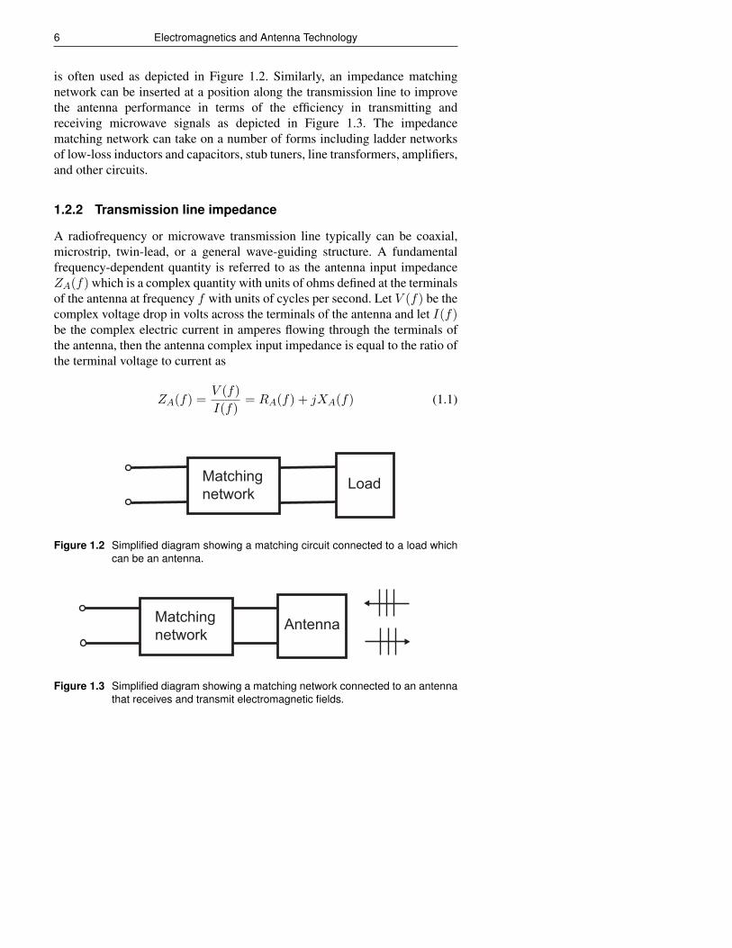
6 Electromagnetics and Antenna Technology
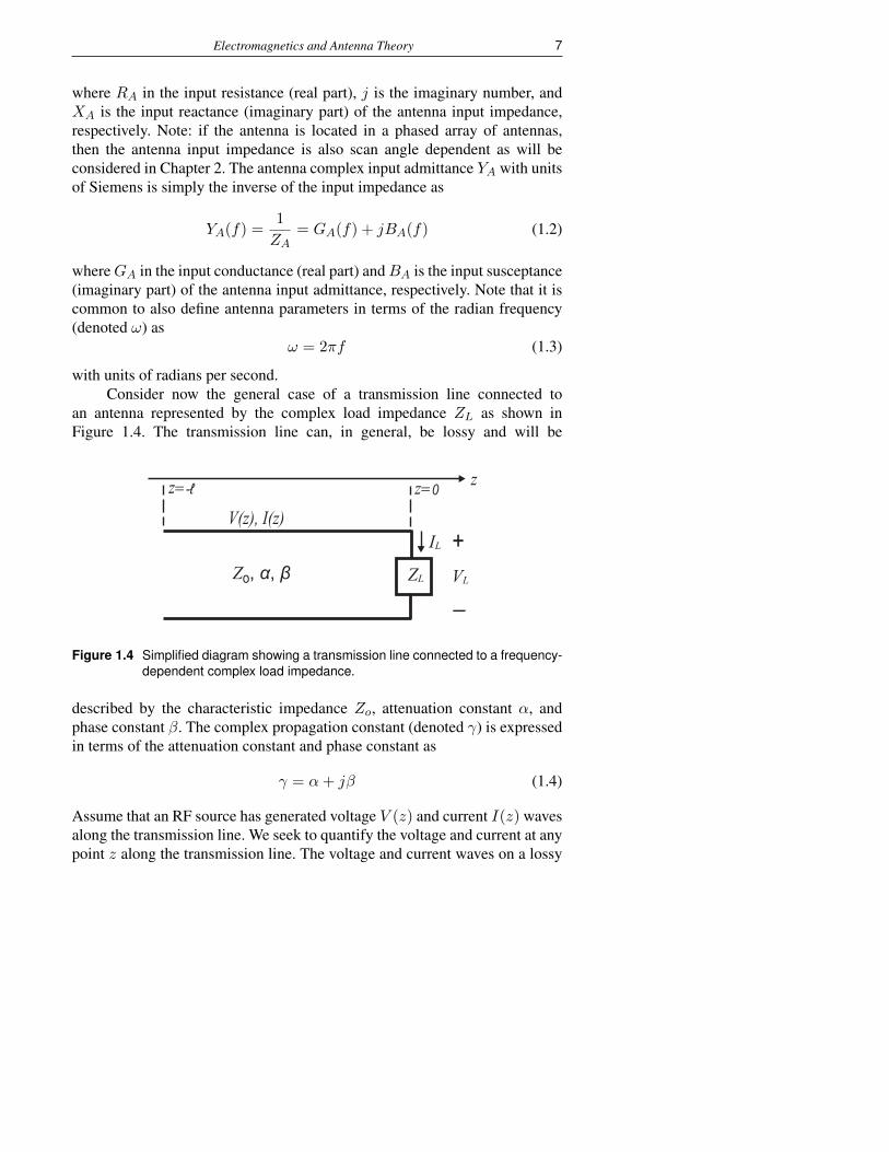
is often used as depicted in Figure 1.2. Similarly, an impedance matchingnetwork can be inserted at a position along the transmission line to improvethe antenna performance in terms of the efficiency in transmitting andreceiving microwave signals as depicted in Figure 1.3. The impedancematching network can take on a number of forms including ladder networksof low-loss inductors and capacitors, stub tuners, line transformers, amplifiers,and other circuits.
1.2.2 Transmission line impedance
A radiofrequency or microwave transmission line typically can be coaxial,microstrip, twin-lead, or a general wave-guiding structure. A fundamentalfrequency-dependent quantity is referred to as the antenna input impedanceZA(f) which is a complex quantity with units of ohms defined at the terminalsof the antenna at frequency f with units of cycles per second. Let V (f) be thecomplex voltage drop in volts across the terminals of the antenna and let I(f)be the complex electric current in amperes flowing through the terminals ofthe antenna, then the antenna complex input impedance is equal to the ratio ofthe terminal voltage to current as
ZA(f) =V (f)
I(f)= RA(f) + jXA(f) (1.1)
Matchingnetwork
Load
Figure 1.2 Simplified diagram showing a matching circuit connected to a load whichcan be an antenna.
Matchingnetwork
Antenna
Figure 1.3 Simplified diagram showing a matching network connected to an antennathat receives and transmit electromagnetic fields.
Electromagnetics and Antenna Theory 7
where RA in the input resistance (real part), j is the imaginary number, andXA is the input reactance (imaginary part) of the antenna input impedance,respectively. Note: if the antenna is located in a phased array of antennas,then the antenna input impedance is also scan angle dependent as will beconsidered in Chapter 2. The antenna complex input admittance YA with unitsof Siemens is simply the inverse of the input impedance as
YA(f) =1
ZA= GA(f) + jBA(f) (1.2)
whereGA in the input conductance (real part) andBA is the input susceptance(imaginary part) of the antenna input admittance, respectively. Note that it iscommon to also define antenna parameters in terms of the radian frequency(denoted ω) as
ω = 2πf (1.3)
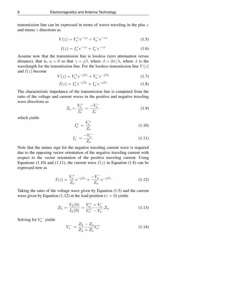
with units of radians per second.Consider now the general case of a transmission line connected to
an antenna represented by the complex load impedance ZL as shown inFigure 1.4. The transmission line can, in general, be lossy and will be
Zo, α, β ZL
V(z), I(z)z=-ℓ
VL
IL +
_
zz=0
Figure 1.4 Simplified diagram showing a transmission line connected to a frequency-dependent complex load impedance.
described by the characteristic impedance Zo, attenuation constant α, andphase constant β. The complex propagation constant (denoted γ) is expressedin terms of the attenuation constant and phase constant as
γ = α+ jβ (1.4)
Assume that an RF source has generated voltage V (z) and current I(z) wavesalong the transmission line. We seek to quantify the voltage and current at anypoint z along the transmission line. The voltage and current waves on a lossy
8 Electromagnetics and Antenna Technology
transmission line can be expressed in terms of waves traveling in the plus zand minus z directions as
V (z) = V +o e−γz + V −o e
−γz (1.5)
I(z) = I+o e−γz + I−o e
−γz (1.6)
Assume now that the transmission line is lossless (zero attenuation versusdistance), that is, α = 0 so that γ = jβ, where β = 2π/λ, where λ is thewavelength for the transmission line. For the lossless transmission line V (z)and I(z) become
V (z) = V +o e−jβz + V −o e
−jβz (1.7)
I(z) = I+o e−jβz + I−o e
−jβz (1.8)
The characteristic impedance of the transmission line is computed from theratio of the voltage and current waves in the positive and negative travelingwave directions as
Zo =V +o
I+o
=−V −oI−o
(1.9)
which yields
I+o =
V +o
Zo(1.10)
I−o =−V −oZo
(1.11)
Note that the minus sign for the negative traveling current wave is requireddue to the opposing vector orientation of the negative traveling current withrespect to the vector orientation of the positive traveling current. UsingEquations (1.10) and (1.11), the current wave I(z) in Equation (1.8) can beexpressed now as
I(z) =V +o
Zoe−jβz +
−V −oZo
e−jβz (1.12)
Taking the ratio of the voltage wave given by Equation (1.5) and the currentwave given by Equation (1.12) at the load position (z = 0) yields
ZL =VL(0)
IL(0)=V +o + V −oV +o − V −o
Zo (1.13)
Solving for V −o yields
V −o =ZL − ZoZL + Zo
V +o (1.14)

Electromagnetics and Antenna Theory 9
The complex voltage reflection coefficient Γ is defined as the ratio of thevoltage wave reflected from the load to the voltage wave incident at the load,that is,
Γ =V −oV +o
=ZL − ZoZL + Zo
(1.15)
The voltage transmission coefficient Tv is defined as the voltage across theload divided by the incident voltage as
Tv =V +o + V −oV +o
= 1 +V −oV +o
= 1 + Γ (1.16)
Now the average incident and reflected powers are given by
P+ =1
2|V +o |2/Zo (1.17)
P− =1
2|V −o |2/Zo (1.18)
The average power actually delivered to the load (same as the average poweraccepted by the load or the average power actually transmitted by a losslessantenna) is equal to the difference between the average incident power and theaverage reflected power, that is,
PL = P+ − P− =1
2|V +o |2/Zo −
1
2|V −o |2/Zo (1.19)
Now dividing the average power delivered to the load by the average incidentpower, which is referred to here as the transmission mismatch efficiencyηtransmission mismatch, yields
PL/P+ = ηtransmission mismatch =
|V +o |2/Zo − |V −o |2/Zo|V +o |2/Zo
(1.20)
which reduces to
ηtransmission mismatch = 1− |V−o |2
|V +o |2
= 1− |Γ|2 (1.21)
The parameter ηtransmission mismatch can be described as the mismatch efficiency(with values ranging from 0 to 1) in transferring power from the transmissionline to the load or antenna, and it represents either power loss or gain loss,depending on its use. The antenna mismatch loss (ML) or realized gain
10 Electromagnetics and Antenna Technology
loss due to mismatch between the antenna load and the transmission line indecibels (dB) is quantifed as
MLdB = 10 log10 ηtransmission mismatch (1.22)
Using Equation (1.15) in Equations (1.7) and (1.8) it follows that
V (z) = V +o (e−jβz + Γejβz) (1.23)
I(z) =V +o
Zo(e−jβz − Γejβz) (1.24)
It can be shown that the maximum and minimum voltages on the transmissionline are expressed as
Vmax = |V +o |(1 + |Γ|) (1.25)
Vmin = |V +o |(1− |Γ|) (1.26)
The voltage standing wave ratio (VSWR) is defined as
VSWR =Vmax
Vmin=
1 + |Γ|1− |Γ|
(1.27)
Solving Equation (1.27) for the magnitude of the reflection coefficient yields
|Γ| = VSWR− 1
VSWR + 1(1.28)
Next, using Equations (1.23) and (1.24), the input impedance Zin at any pointalong the transmission line is now expressed as
Zin(−l) =V (−l)I(−l)
=V +o (ejβl + Γe−jβl)
V +o (ejβl − Γe−jβl)
Zo =1 + Γe−j2βl
1− Γe−j2βlZo (1.29)
Subsituting Equation (1.15) in Equation (1.29) yields after simplification
Zin(−l) = ZoZL + jZo tanβl
Zo + jZL tanβl(1.30)
In the general case with frequency dependence, if an antenna withcomplex input impedance ZA is connected to a transmission line with char-acteristic impedance Zo, then the antenna’s frequency-dependent complexreflection coefficient ΓA is given by
ΓA(f) =ZA(f)− Zo(f)
ZA(f) + Zo(f)(1.31)
Electromagnetics and Antenna Theory 11
It should be noted that the characteristic impedance of a coaxial transmissionline or microstrip line is frequency independent, whereas in a rectangular orcircular waveguide the characteristic impedance is frequency dependent. Inthis book, we concentrate primarily on antennas that are connected to a coaxialtransmission line.
Impedance matching is a critical technique that is used to improve theperformance of antennas. Figure 2 shows the situation in which a two-portmatching network is connected at a position along the transmission that isconnected to the antenna. To reduce impedance mismatch effects betweenthe transmission line and the antenna, the parameters of the matching devicecan be adjusted so that the reflection coefficient magnitude is minimized. Asignificant amount of impedance matching theory has been developed by priorresearchers. In this book, some general theory of impedance matching theoryis given as well as specific applied examples for narrowband and widebandantennas.
1.2.3 Smith chart theory
In this book, impedance data are presented either in the form of a rectangularplot with the horizontal axis the real part of the impedance and the verticalaxis the imaginary part of the impedance, or as in a Smith chart [63 – 66] asis described in this section. In a Smith chart, the impedance data are typicallynormalized by the charateristic impedance of a transmission line. A derivationof the Smith chart equations is now given.
The derivation starts by normalizing the right-hand side of the voltagereflection coefficient Equation (1.15) by Zo with the result
Γ =zL − 1
zL + 1(1.32)
where zL = ZL/Zo is the normalized impedance. Now solving Equa-tion (1.32) for zL yields
zL =1 + Γ
1− Γ(1.33)
Expressing the normalized load impedance and the reflection cofficient interms of real and imaginary components as zL = rL + jxL and Γ = Γr + jΓiEquation (1.33) becomes
zL = rL + jxL =1 + Γ
1− Γ=
(1 + Γr) + jΓi(1− Γr)− jΓi
(1.34)
Now, multiplying the top and bottom of the right-hand side of Equation (1.34)by the complex conjugate of the denominator, and then simplifying and

12 Electromagnetics and Antenna Technology
equating real and imaginary components with rL and xL yields
rL =(1− Γ2
r)− Γ2i
(1− Γr)2 + Γ2i
(1.35)
xL =2Γi
(1− Γr)2 + Γ2i
(1.36)
By rearranging terms and factoring, Equations (1.35) and (1.36) can be putinto the standard form for constant resistance circles as(
Γr −rL
rL + 1
)2
+ Γ2i =
(1
rL + 1
)2
(1.37)
which is centered atΓr =
rLrL + 1
Γi = 0 (1.38)
and has radius1
rL + 1(1.39)
and for constant reactance circles as
(Γr − 1)2 +
(Γi −
1
xL
)2
=
(1
xL
)2
(1.40)
which is centered atΓr = 1 Γi =
1
xL(1.41)
and has radius1
xL(1.42)
Similarly, in a Smith chart, the admittance data are typically normalizedby the charateristic admittance of a transmission line. The derivation startsby normalizing the right-hand side of Equation (1.15) by Zo and then usingzL = 1/yL with the result
Γ =zL − 1
zL + 1=
1/yL − 1
1/yL + 1=
1− yL1 + yL
(1.43)
where yL is the normalized impedance. Now solving Equation (1.43) for yLyields
yL =1− Γ
1 + Γ(1.44)
Electromagnetics and Antenna Theory 13
Expressing the normalized load impedance and the reflection cofficient interms of real and imaginary components as yL = gL + jbL and Γ = Γr + jΓiEquation (1.44) becomes
yL = gL + jbL =1− Γ
1 + Γ=
(1− Γr)− jΓi(1 + Γr) + jΓi
(1.45)
Now, multiplying the top and bottom of the right-hand side of Equation (1.45)by the complex conjugate of the denominator, and then simplifying andequating real and imaginary components with gL and bL yields
gL =(1− Γ2
r)− Γ2i
(1 + Γr)2 + Γ2i
(1.46)
bL = − 2Γi(1− Γr)2 + Γ2
i
(1.47)
By rearranging terms and factoring, Equations (1.47) and (1.35) can be putinto the standard form for constant conductance circles as(
Γr +gL
gL + 1
)2
+ Γ2i =
(1
gL + 1
)2
(1.48)
which is centered atΓr = − gL
gL + 1Γi = 0 (1.49)
and has radius1
gL + 1(1.50)
and for constant susceptance circles as
(Γr + 1)2 +
(Γi +
1
bL
)2
=
(1
bL
)2
(1.51)
which is centered atΓr = −1 Γi = − 1
bL(1.52)
and has radius1
bL(1.53)
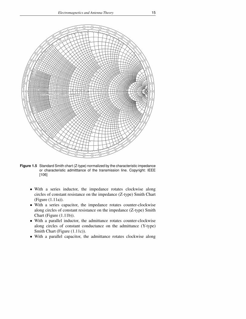
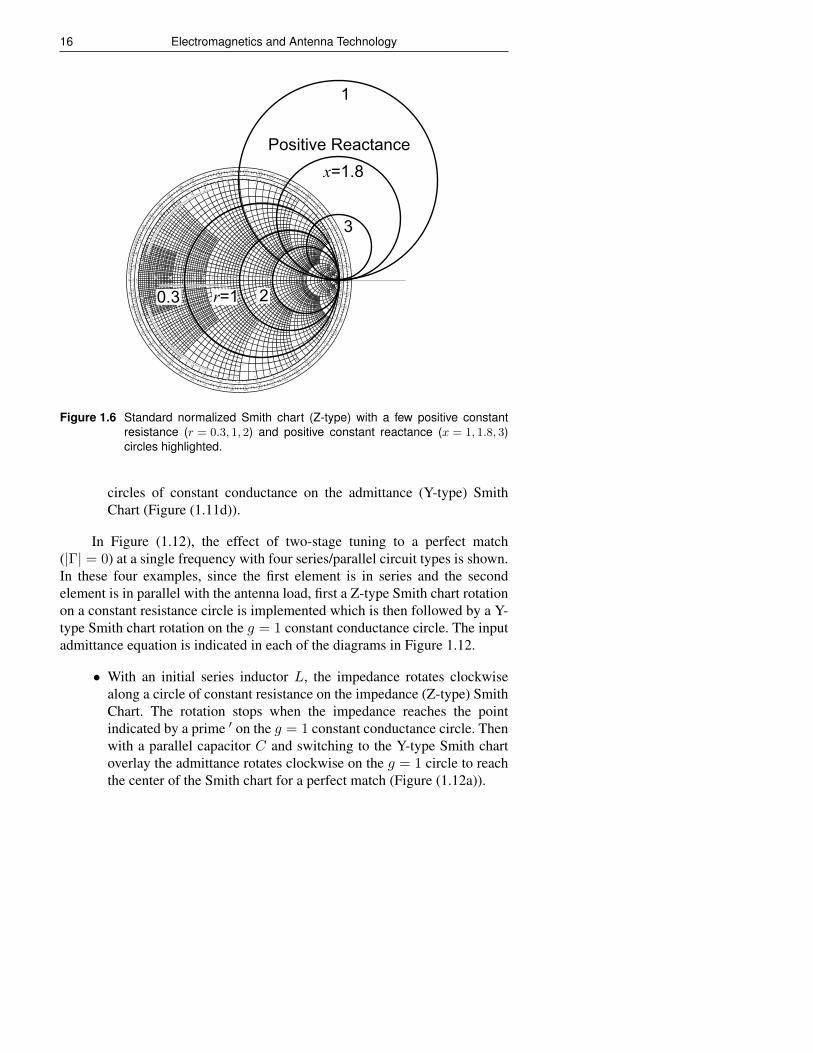
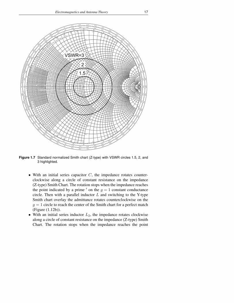
A standard Smith chart normalized by the characteristic impedance orcharacteristic admitttance of the transmission line is shown in Figure 1.5.This type of Smith chart is referred to here as a Z-type Smith Chart.The same Z-type of Smith chart is repeated in Figure 1.6, but now with
14 Electromagnetics and Antenna Technology
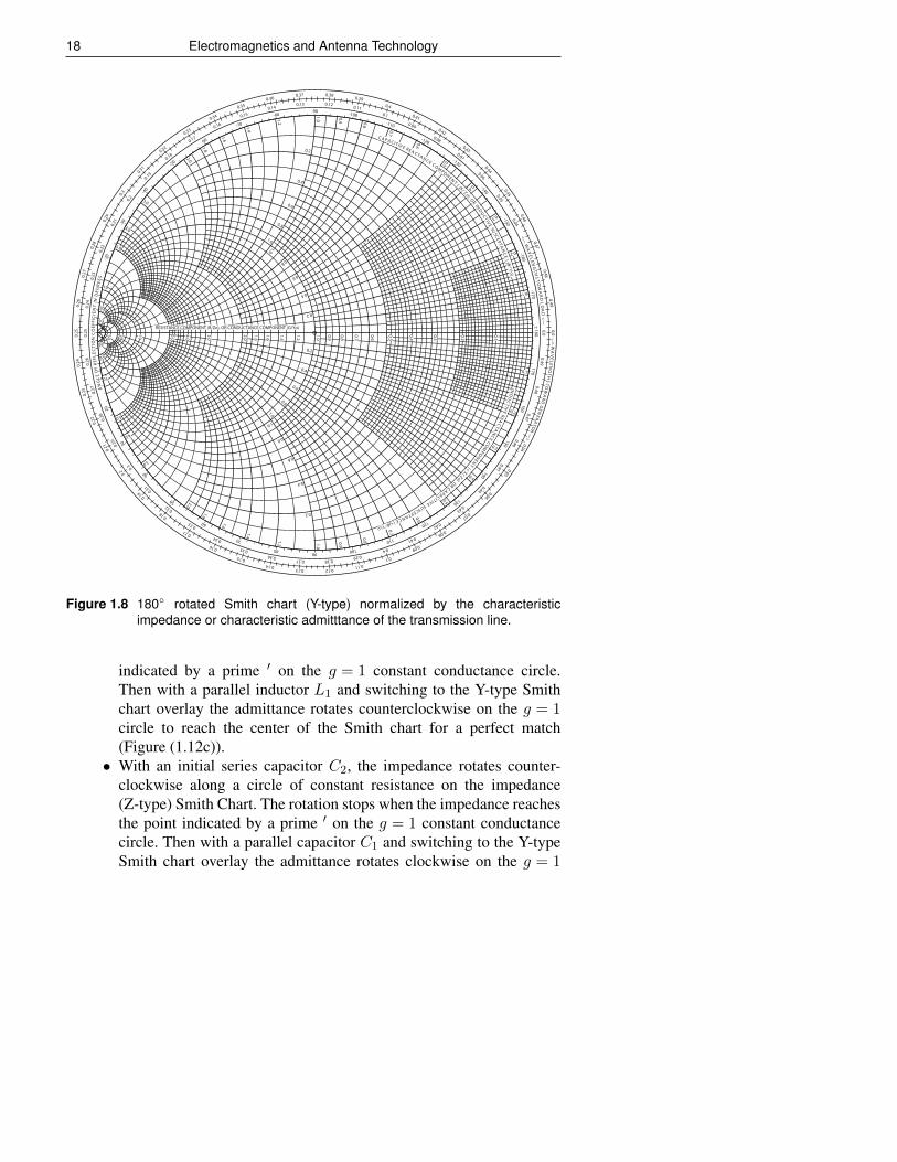
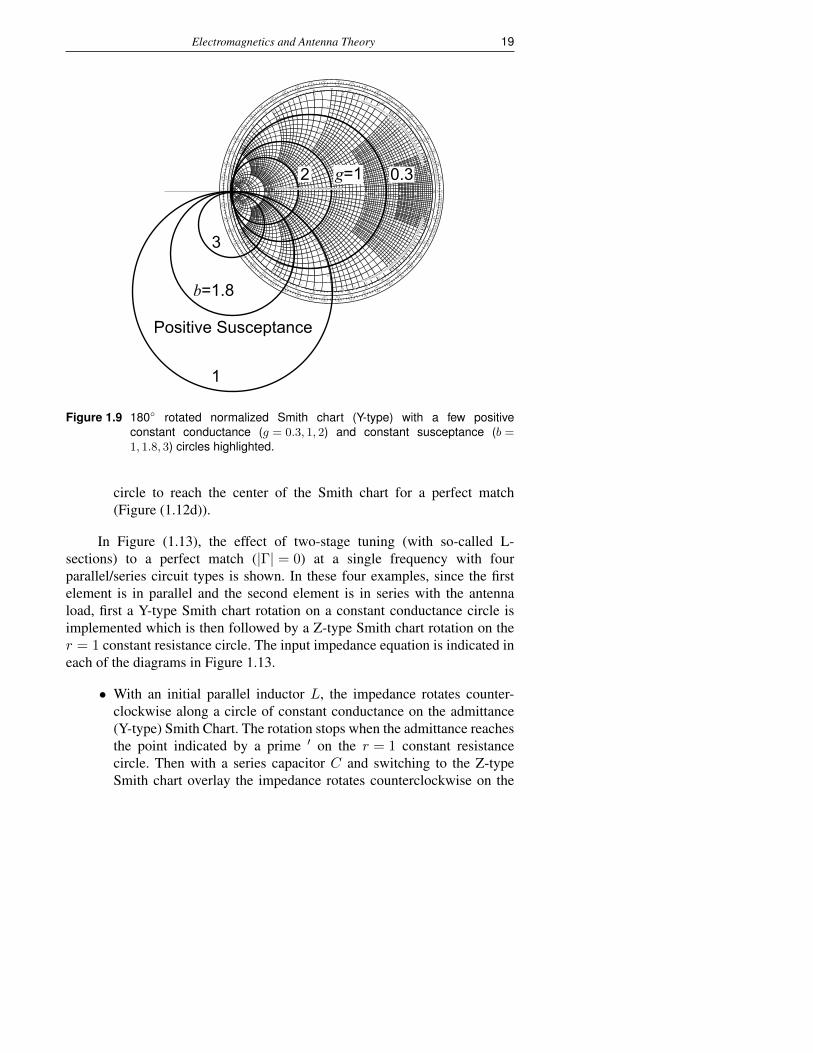
constant resistance (r = 0.3, 1, 2) and positive constant reactance (x =1, 1.8, 3) circles highlighted. Figure 1.7 shows a standard normalized Smithchart (Z-type) with VSWR circles 1.5, 2, and 3 highlighted. As mentioned,the standard Z-type Smith chart can be used to analyze impedance andadmittance data. When impedance values are plotted in a Z-type Smithchart, the corresponding admittance values are positioned 180 away fromthe impedance values on a constant VSWR circle. An alternate method forworking with admittance values, is to physically rotate the Smith chart by180. A 180 rotated Smith chart normalized by the characteristic impedanceor characteristic admitttance of the transmission line is shown in Figure 1.8.This type of Smith chart is referred to here as a Y-type Smith Chart (someauthors [72] refer to this type of Smith Chart presentation as an overlay),because the chart is used directly with the admittance circles. The same Y-type Smith chart is repeated in Figure 1.9, but now with constant conductance(g = 0.3, 1, 2) and constant susceptance (b = 1, 1.8, 3) circles highlighted.Note: The MATLAB RF Toolbox (www.mathworks.com) provides Smithcharts of the following type: Z-type, Y-type, ZY-type (Z is the primary chartwith Y the overlay), and YZ-type (Y is the primary chart with Z the overlay).
1.2.4 Impedance Matching Circuit Elements
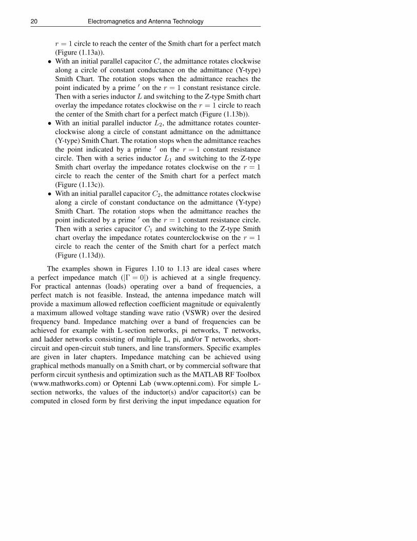
Impedance matching [67–75] is an important part of antenna technology, asit can be used to improve the transmit and receive characteristics of antennasover a bandwidth of interest. To improve the impedance match of an antennato a transmission line of characteristic impedance Zo, it is common to use oneor more inductors and/or capacitors in series or in parallel with the antenna.These circuit elements are placed as close to the antenna terminals as possibleto reduce dispersive effects and allow improved impedance matching over agiven bandwidth. Let L be the inductance (typically in nH) of an inductor andlet C be the capacitance (typically in pF) of a capacitor. Let ZA be the antennainput impedance. It follows then that
• A series inductor provides an impedance equal to jωL and a seriescapacitor provides an impedance equal to 1/(jωC).
• A parallel inductor provides an admittance equal to 1/(jωL) and aparallel capacitor provides an admittance equal to jωC.
Figure (1.10) summarizes the input impedance Zin for these four circuittypes with either a single inductor or single capacitor in series or parallelto the antenna (load) impedance ZA. The corresponding Smith charts inFigure (1.11) show the effect of tuning to a perfect match (|Γ| = 0) at a singlefrequency with these four circuit types.
Electromagnetics and Antenna Theory 15
j
,
20-20
30-30
40-40
50
-50
60
-60
70
-70
80
-80
90
-90
100
-100
110
-110
120
-120
130
-130
140-1
40
150
-150
160
-160
170
-170
180
0.04
0.04
0.05
0.05
0.06
0.06
0.07
0.07
0.08
0.08
0.09
0.09
0.1
0.1
0.11
0.11
0.12
0.12
0.13
0.13
0.14
0.14
0.15
0.15
0.16
0.16
0.17
0.17
0.18
0.18
0.190.19
0.20.2
0.21
0.210.22
0.220.23
0.230.24
0.24
0.25
0.25
0.26
0.26
0.27
0.27
0.28
0.28
0.29
0.29
0.3
0.3
0.31
0.31
0.32
0.32
0.33
0.33
0.34
0.34
0.35
0.35
0.36
0.36
0.37
0.37
0.38
0.38
0.39
0.39
0.4
0.4
0.41
0.41
0.42
0.42
0.43
0.43
0.440.44
0.45
0.45
0.46
0.46
0.47
0.47
0.48
0.48
0.49
0.49
0.0
0.0
AN
GLE
OF
RE
FLE
CT
ION
CO
EFFIC
IEN
TIN
DEG
REES
—>
WA
VE
LE
NG
THS
TOW
AR
DG
ENER
ATO
R—
><—
WA
VEL
ENG
THS
TOW
AR
DL
OA
D<—
I
IT
ND
UC
TIV
ER
EAC
TAN
CE
COM
PON
EN(+
X/ Zo) OR
CA PA CTIV E SU SC EPTA N C E (+jB/ Y o)
CAPACITIVEREACTANCECOMPONENT(-j
X/Zo),OR
IND
UCTIV
ESU
SCEP
TAN
CE
(-jB
/Yo)
0.1
0.1
0.1
0.2
0.2
0.2
0.3
0.3
0.3
0.4
0.4
0.4
0.50.5
0.5
0.6
0.6
0.6
0.7
0.7
0.7
0.8
0.8
0.8
0.9
0.9
0.9
1.0
1.0
1.0
1.2
1.2
1.2
1.4
1.4
1.4
1.6
1.6
1.6
1.8
1.8
1.8
2.02.0
2.0
3.0
3.0
3.0
4.0
4.0
4.0
5.0
5.0
5.0
10
10
10
20
20
20
50
50
50
0.2
0.2
0.2
0.2
0.4
0.4
0.4
0.4
0.6
0.6
0.6
0.6
0.8
0.8
0.8
0.8
1.0
1.0
1.01.0
RESISTANCE COMPONENT (R/Zo), OR CONDUCTANCE COMPONENT (G/Yo)
±
Figure 1.5 Standard Smith chart (Z-type) normalized by the characteristic impedanceor characteristic admitttance of the transmission line. Copyright: IEEE[106]
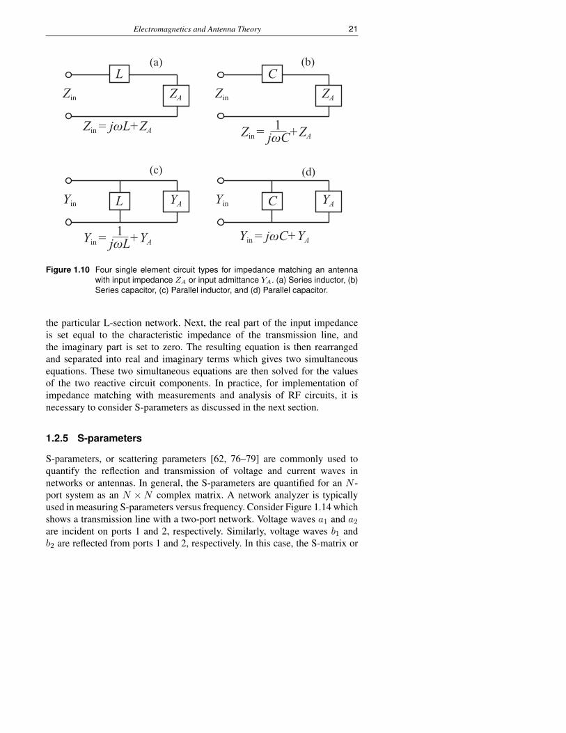
• With a series inductor, the impedance rotates clockwise alongcircles of constant resistance on the impedance (Z-type) Smith Chart(Figure (1.11a)).• With a series capacitor, the impedance rotates counter-clockwise
along circles of constant resistance on the impedance (Z-type) SmithChart (Figure (1.11b)).• With a parallel inductor, the admittance rotates counter-clockwise
along circles of constant conductance on the admittance (Y-type)Smith Chart (Figure (1.11c)).• With a parallel capacitor, the admittance rotates clockwise along
16 Electromagnetics and Antenna Technology
j
,
20-20
30-30
40-40
50
-50
60
-60
70
-70
80
-80
90
-90
100
-100
110
-110
120
-120
130
-130
140-1
40
150
-150
160
-160
170
-170
180
0.04
0.04
0.05
0.05
0.06
0.06
0.07
0.07
0.08
0.08
0.09
0.09
0.1
0.1
0.11
0.11
0.12
0.12
0.13
0.13
0.14
0.14
0.15
0.15
0.16
0.16
0.17
0.17
0.18
0.18
0.190.19
0.20.2
0.210.21
0.22
0.220.23
0.230.24
0.24
0.25
0.25
0.26
0.26
0.27
0.27
0.28
0.28
0.29
0.29
0.3
0.3
0.31
0.31
0.32
0.32
0.33
0.33
0.34
0.34
0.35
0.35
0.36
0.36
0.37
0.37
0.38
0.38
0.39
0.39
0.4
0.4
0.41
0.41
0.42
0.42
0.43
0.43
0.440.44
0.45
0.45
0.46
0.46
0.47
0.47
0.48
0.48
0.49
0.49
0.0
0.0
AN
GL
EO
FR
EFLE C
TION
CO
EFFI CIE
NT
IND
EG
RE
ES
—>
WA
VE L
EN
GT H
STO
WA
RD
GEN
ERA
TOR
—>
<—W
AV
ELE
NG
THS
TO
WA
RD
LO
AD
<—
I
I
T
ND
UC
TIV
ER
EAC
TAN
CE
COM
PON
EN(+
X/ Zo) OR C A PA C
T IVE SU SC EPT A N CE (+jB / Y o)
CAPACITIVEREACTANCECOMPONENT(-j
X/Zo),ORIN
DU
CTIVE
SUSC
EPTA
NC
E(-
jB/Y
o)
0.1
0.1
0.1
0.2
0.2
0.2
0.3
0.3
0.3
0.4
0.4
0.4
0.50.5
0.5
0.6
0.6
0.6
0.7
0.7
0.7
0.8
0.8
0.8
0.9
0.9
0.9
1.0
1.0
1.0
1.2
1.2
1.2
1.4
1.4
1.4
1.6
1.6
1.6
1.8
1.8
1.8
2.02.0
2.0
3.0
3.0
3.0
4.0
4.0
4.0
5.0
5.0
5.0
10
10
10
20
20
20
50
50
50
0.2
0.2
0.2
0.2
0.4
0.4
0.4
0.4
0.6
0.6
0.6
0.6
0.8
0.8
0.8
0.8
1.0
1.0
1.01.0
RESISTANCE COMPONENT (R/Zo), OR CONDUCTANCE COMPONENT (G/Yo)
±
3
x=1.8
1
r=1 20.3
Positive Reactance
Figure 1.6 Standard normalized Smith chart (Z-type) with a few positive constantresistance (r = 0.3, 1, 2) and positive constant reactance (x = 1, 1.8, 3)circles highlighted.
circles of constant conductance on the admittance (Y-type) SmithChart (Figure (1.11d)).
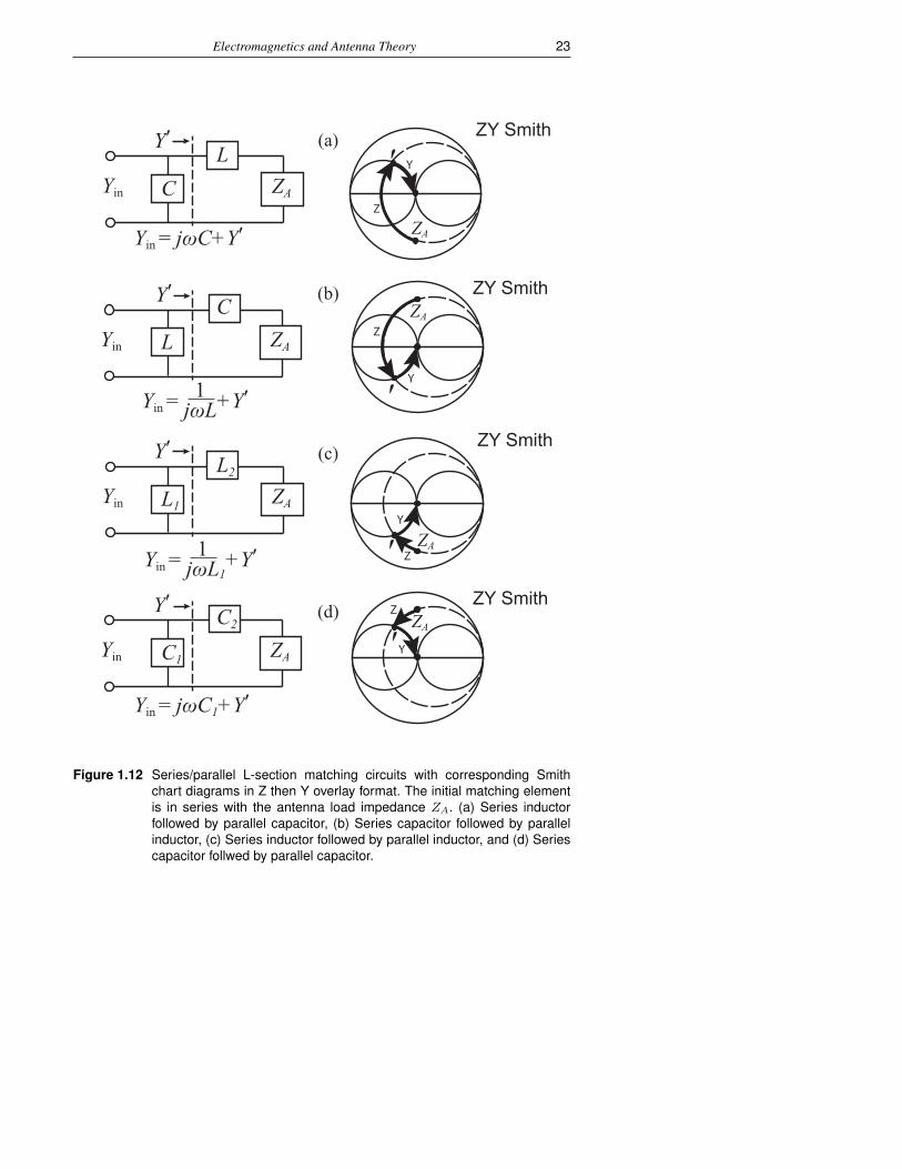
In Figure (1.12), the effect of two-stage tuning to a perfect match(|Γ| = 0) at a single frequency with four series/parallel circuit types is shown.In these four examples, since the first element is in series and the secondelement is in parallel with the antenna load, first a Z-type Smith chart rotationon a constant resistance circle is implemented which is then followed by a Y-type Smith chart rotation on the g = 1 constant conductance circle. The inputadmittance equation is indicated in each of the diagrams in Figure 1.12.
• With an initial series inductor L, the impedance rotates clockwisealong a circle of constant resistance on the impedance (Z-type) SmithChart. The rotation stops when the impedance reaches the pointindicated by a prime ′ on the g = 1 constant conductance circle. Thenwith a parallel capacitor C and switching to the Y-type Smith chartoverlay the admittance rotates clockwise on the g = 1 circle to reachthe center of the Smith chart for a perfect match (Figure (1.12a)).
Electromagnetics and Antenna Theory 17
j
,
20-20
30-30
40-40
50
-50
60
-60
70
-70
80
-80
90
-90
100
-100
110
-110
120
-120
130
-130
140-1
40
150
-150
160
-160
170
-170
180
0.04
0.04
0.05
0.05
0.06
0.06
0.07
0.07
0.08
0.08
0.09
0.09
0.1
0.1
0.11
0.11
0.12
0.12
0.13
0.13
0.14
0.14
0.15
0.15
0.16
0.16
0.17
0.17
0.18
0.18
0.190.19
0.20.2
0.210.21
0.22
0.220.23
0.230.24
0.24
0.25
0.25
0.26
0.26
0.27
0.27
0.28
0.28
0.29
0.29
0.3
0.3
0.31
0.31
0.32
0.32
0.33
0.33
0.34
0.34
0.35
0.35
0.36
0.36
0.37
0.37
0.38
0.38
0.39
0.39
0.4
0.4
0.41
0.41
0.42
0.42
0.43
0.43
0.440.44
0.45
0.45
0.46
0.46
0.47
0.47
0.48
0.48
0.49
0.49
0.0
0.0
AN
GL
EO
FR
EFLE C
TION
CO
EFFI CIE
NT
IND
EG
RE
ES
—>
WA
VE L
EN
GTH
STO
WA
RD
GEN
ERA
TOR
—>
<—W
AV
ELEN
GTH
ST
OW
AR
DLO
AD
<—
I
IT
ND
UC
TIV
ER
EAC
TAN
CE
COM
PON
EN(+
X/ Zo) OR C A PA C
T IV E SU SC EPT A N CE (+jB/ Y o)
CAPACITIVEREACTANCECOMPONENT(-j
X/Zo),OR
IND
UCTI
VE
SUSC
EPTA
NC
E(-
jB/Y
o)
0.1
0.1
0.1
0.2
0.2
0.2
0.3
0.3
0.3
0.4
0.4
0.4
0.50.5
0.5
0.6
0.6
0.6
0.7
0.7
0.7
0.8
0.8
0.8
0.9
0.9
0.9
1.0
1.0
1.0
1.2
1.2
1.2
1.4
1.4
1.4
1.6
1.6
1.6
1.8
1.8
1.8
2.02.0
2.0
3.0
3.0
3.0
4.0
4.0
4.0
5.0
5.0
5.0
10
10
10
20
20
20
50
50
50
0.2
0.2
0.2
0.2
0.4
0.4
0.4
0.4
0.6
0.6
0.6
0.6
0.8
0.8
0.8
0.8
1.0
1.0
1.01.0
RESISTANCE COMPONENT (R/Zo), OR CONDUCTANCE COMPONENT (G/Yo)
±
VSWR=3
2
1.5
Figure 1.7 Standard normalized Smith chart (Z-type) with VSWR circles 1.5, 2, and3 highlighted.
• With an initial series capacitor C, the impedance rotates counter-clockwise along a circle of constant resistance on the impedance(Z-type) Smith Chart. The rotation stops when the impedance reachesthe point indicated by a prime ′ on the g = 1 constant conductancecircle. Then with a parallel inductor L and switching to the Y-typeSmith chart overlay the admittance rotates counterclockwise on theg = 1 circle to reach the center of the Smith chart for a perfect match(Figure (1.12b)).• With an initial series inductor L2, the impedance rotates clockwise
along a circle of constant resistance on the impedance (Z-type) SmithChart. The rotation stops when the impedance reaches the point
18 Electromagnetics and Antenna Technology
j
,
20-2
0
30-3
0
40-4
0
50
-50
60
-60
70
-70
80
-80
90
-90
100
-100
110
-110
120
-120
130
-130
140-140
150-150
160-160
170-170
180
0.04
0.04
0.05
0.05
0.06
0.06
0.07
0.07
0.08
0.08
0.09
0.09
0.1
0.1
0.11
0.11
0.12
0.12
0.13
0.13
0.14
0.14
0.15
0.15
0.16
0.16
0.17
0.17
0.18
0.18
0.190.19
0.20.2
0.21
0.21
0.22
0.22
0.23
0.23
0.24
0.24
0.25
0.25
0.26
0.26
0.27
0.27
0.28
0.28
0.29
0.29
0.3
0.3
0.31
0.31
0.32
0.32
0.33
0.33
0.34
0.34
0.35
0.35
0.36
0.36
0.37
0.37
0.38
0.38
0.39
0.39
0.4
0.4
0.41
0.41
0.42
0.42
0.43
0.43
0.440.44
0.450.45
0.46
0.460.47
0.470.48
0.480.49
0.49
0.0
0.0
AN
GL
EO
FR
EFL
ECT
ION
CO
E FF I
CIE
NT
IND
EG
RE
E S
—>
WA
VELE
NG
THS
TOW
AR
DG
ENER
ATO
R—
><—
WA
VE LEN
GTH
ST
OW
AR
DL O
AD
<—
I
I
T
ND
UC
TIVE
REA
CTA
NC
ECO
MPO
NEN
(+X/Zo) ORCAPAC
TIVESUSCEPTANCE(+jB/Yo)
C A PA CIT IV E R EA CT A N CE COM PON E NT (-jX/ Zo), ORIN
DU
CTIVE
SUSC
EPTAN
CE
(-jB / Yo)
0.1
0.1
0.1
0.2
0.2
0.2
0.3
0.3
0.3
0.4
0.4
0.4
0.50.5
0.5
0.60.6
0.6
0.70.7
0.7
0.80.8
0.80.9
0.9
0.9
1.01.0
1.0
1.21.2
1.2
1.41.4
1.4
1.61.6
1.6
1.81.8
1.8
2.02.0
2.0
3.0
3.0
3.0
4.0
4.0
4.0
5.0
5.0
5.0
10
10
10
20
20
20
50
50
50
0.2
0.2
0.2
0.2
0.4
0.4
0.4
0.4
0.6
0.6
0.6
0.6
0.8
0.8
0.8
0.8
1.0
1.0
1.01.0
RESISTANCE COMPONENT (R/Zo), OR CONDUCTANCE COMPONENT (G/Yo)
±
Figure 1.8 180 rotated Smith chart (Y-type) normalized by the characteristicimpedance or characteristic admitttance of the transmission line.
indicated by a prime ′ on the g = 1 constant conductance circle.Then with a parallel inductor L1 and switching to the Y-type Smithchart overlay the admittance rotates counterclockwise on the g = 1circle to reach the center of the Smith chart for a perfect match(Figure (1.12c)).
• With an initial series capacitor C2, the impedance rotates counter-clockwise along a circle of constant resistance on the impedance(Z-type) Smith Chart. The rotation stops when the impedance reachesthe point indicated by a prime ′ on the g = 1 constant conductancecircle. Then with a parallel capacitor C1 and switching to the Y-typeSmith chart overlay the admittance rotates clockwise on the g = 1
Electromagnetics and Antenna Theory 19
j
,
20-2
0
30-3
0
40-4
0
50
-50
60
-60
70
-70
80
-80
90
-90
100
-100
110
-110
120
-120
130
-130
140-140
150-150
160-160
170-170
180
0.04
0.04
0.05
0.05
0.06
0.06
0.07
0.07
0.08
0.08
0.09
0.09
0.1
0.1
0.11
0.11
0.12
0.12
0.13
0.13
0.14
0.14
0.15
0.15
0.16
0.16
0.17
0.17
0.18
0.18
0.190.19
0.20.2
0.21
0.21
0.22
0.22
0.23
0.23
0.24
0.24
0.25
0.25
0.26
0.26
0.27
0.27
0.28
0.28
0.29
0.29
0.3
0.3
0.31
0.31
0.32
0.32
0.33
0.33
0.34
0.34
0.35
0.35
0.36
0.36
0.37
0.37
0.38
0.38
0.39
0.39
0.4
0.4
0.41
0.41
0.42
0.42
0.43
0.43
0.440.44
0.450.45
0.46
0.460.47
0.470.48
0.480.49
0.49
0.0
0.0
AN
GL
EO
FR
EFL
ECTI
ON
CO
E FF I
CIE
NT
IND
EG
RE
E S
—>
WA
VELE
NG
THS
TOW
AR
DG
ENERA
TOR
—>
<—W
AV
ELEN
GTH
ST
OW
AR
DL
OA
D<
—
I
I
T
ND
UC
TIV
ER
EAC
TAN
CE
COM
PON
EN(+
X/Zo) ORCAPACTIVESUSCEPTANCE(+jB/Yo)
C A PA CI T IV E RE A CT A N CE COMPONE NT (- jX/ Zo), ORIN
DU
CTIVE
SUSC
EP TAN
CE
(-jB/Y
o)
0.1
0.1
0.1
0.2
0.2
0.2
0.3
0.3
0.3
0.4
0.4
0.4
0.50.5
0.5
0.60.6
0.6
0.70.7
0.7
0.80.8
0.80.9
0.9
0.9
1.01.0
1.0
1.21.2
1.2
1.41.4
1.4
1.61.6
1.6
1.81.8
1.8
2.02.0
2.0
3.0
3.0
3.0
4.0
4.0
4.0
5.0
5.0
5.0
10
10
10
20
20
20
50
50
50
0.2
0.2
0.2
0.2
0.4
0.4
0.4
0.4
0.6
0.6
0.6
0.6
0.8
0.8
0.8
0.8
1.0
1.0
1.01.0
±
3
b=1.8
1
g=12 0.3RESISTANCE COMPONENT (R/Zo), OR CONDUCTANCE COMPONENT (G/Yo)
Positive Susceptance
Figure 1.9 180 rotated normalized Smith chart (Y-type) with a few positiveconstant conductance (g = 0.3, 1, 2) and constant susceptance (b =1, 1.8, 3) circles highlighted.
circle to reach the center of the Smith chart for a perfect match(Figure (1.12d)).
In Figure (1.13), the effect of two-stage tuning (with so-called L-sections) to a perfect match (|Γ| = 0) at a single frequency with fourparallel/series circuit types is shown. In these four examples, since the firstelement is in parallel and the second element is in series with the antennaload, first a Y-type Smith chart rotation on a constant conductance circle isimplemented which is then followed by a Z-type Smith chart rotation on ther = 1 constant resistance circle. The input impedance equation is indicated ineach of the diagrams in Figure 1.13.
• With an initial parallel inductor L, the impedance rotates counter-clockwise along a circle of constant conductance on the admittance(Y-type) Smith Chart. The rotation stops when the admittance reachesthe point indicated by a prime ′ on the r = 1 constant resistancecircle. Then with a series capacitor C and switching to the Z-typeSmith chart overlay the impedance rotates counterclockwise on the
20 Electromagnetics and Antenna Technology
r = 1 circle to reach the center of the Smith chart for a perfect match(Figure (1.13a)).
• With an initial parallel capacitor C, the admittance rotates clockwisealong a circle of constant conductance on the admittance (Y-type)Smith Chart. The rotation stops when the admittance reaches thepoint indicated by a prime ′ on the r = 1 constant resistance circle.Then with a series inductor L and switching to the Z-type Smith chartoverlay the impedance rotates clockwise on the r = 1 circle to reachthe center of the Smith chart for a perfect match (Figure (1.13b)).
• With an initial parallel inductor L2, the admittance rotates counter-clockwise along a circle of constant admittance on the admittance(Y-type) Smith Chart. The rotation stops when the admittance reachesthe point indicated by a prime ′ on the r = 1 constant resistancecircle. Then with a series inductor L1 and switching to the Z-typeSmith chart overlay the impedance rotates clockwise on the r = 1circle to reach the center of the Smith chart for a perfect match(Figure (1.13c)).
• With an initial parallel capacitor C2, the admittance rotates clockwisealong a circle of constant conductance on the admittance (Y-type)Smith Chart. The rotation stops when the admittance reaches thepoint indicated by a prime ′ on the r = 1 constant resistance circle.Then with a series capacitor C1 and switching to the Z-type Smithchart overlay the impedance rotates counterclockwise on the r = 1circle to reach the center of the Smith chart for a perfect match(Figure (1.13d)).
The examples shown in Figures 1.10 to 1.13 are ideal cases wherea perfect impedance match (|Γ = 0|) is achieved at a single frequency.For practical antennas (loads) operating over a band of frequencies, aperfect match is not feasible. Instead, the antenna impedance match willprovide a maximum allowed reflection coefficient magnitude or equivalentlya maximum allowed voltage standing wave ratio (VSWR) over the desiredfrequency band. Impedance matching over a band of frequencies can beachieved for example with L-section networks, pi networks, T networks,and ladder networks consisting of multiple L, pi, and/or T networks, short-circuit and open-circuit stub tuners, and line transformers. Specific examplesare given in later chapters. Impedance matching can be achieved usinggraphical methods manually on a Smith chart, or by commercial software thatperform circuit synthesis and optimization such as the MATLAB RF Toolbox(www.mathworks.com) or Optenni Lab (www.optenni.com). For simple L-section networks, the values of the inductor(s) and/or capacitor(s) can becomputed in closed form by first deriving the input impedance equation for
Electromagnetics and Antenna Theory 21
LZAZin
Zin = jωL+ZA
CZAZin
Zin = jωC+ZA1
L YAYin
Yin = jωC+YA
C YAYin
Yin = jωL+YA1
(a)
(d)(c)
(b)
Figure 1.10 Four single element circuit types for impedance matching an antennawith input impedance ZA or input admittance YA. (a) Series inductor, (b)Series capacitor, (c) Parallel inductor, and (d) Parallel capacitor.
the particular L-section network. Next, the real part of the input impedanceis set equal to the characteristic impedance of the transmission line, andthe imaginary part is set to zero. The resulting equation is then rearrangedand separated into real and imaginary terms which gives two simultaneousequations. These two simultaneous equations are then solved for the valuesof the two reactive circuit components. In practice, for implementation ofimpedance matching with measurements and analysis of RF circuits, it isnecessary to consider S-parameters as discussed in the next section.
1.2.5 S-parameters
S-parameters, or scattering parameters [62, 76–79] are commonly used toquantify the reflection and transmission of voltage and current waves innetworks or antennas. In general, the S-parameters are quantified for an N -port system as an N ×N complex matrix. A network analyzer is typicallyused in measuring S-parameters versus frequency. Consider Figure 1.14 whichshows a transmission line with a two-port network. Voltage waves a1 and a2
are incident on ports 1 and 2, respectively. Similarly, voltage waves b1 andb2 are reflected from ports 1 and 2, respectively. In this case, the S-matrix or
22 Electromagnetics and Antenna Technology
LZAZin
Zin = jωL+ZA
(a)
CZAZin
Zin = jωC+ZA1
(b)
L YAYin
Yin = jωL+YA1
(c)
Yin = jωC+YA
C YAYin
(d)
ZA
ZA
YA
–j
+j
YA
–j
+j
Z Smith
Z Smith
Y Smith
Y Smith
–j
+j
–j
+j
Figure 1.11 Series L or C circuits with corresponding Z and Y Smith chart diagrams.(a) Series inductor, (b) Series capacitor, (c) Parallel inductor, and (d)Parallel capacitor.
scattering matrix is a 2 x 2 complex matrix that is expressed as
S =
[S11 S12S21 S22
]. (1.54)
Electromagnetics and Antenna Theory 23
LZAYin
Yin = jωC+Yʹ
CZAYin
Yin = jωL+Yʹ1
C
L
(a)
(b)
(c)
(d)
ZA
ZA
ZY Smith
ZY Smith
Z
Y
Z
Y
L2
ZAYin
Yin = jωC1+Yʹ
C2
ZAYin
L1
C1
ZA
ZA
ZY Smith
ZY Smith
Z
Y
Z
Y
Yin = jωL1+Yʹ1
Yʹ
Yʹ
Yʹ
Yʹ
ʹ
ʹ
ʹ
ʹ
Figure 1.12 Series/parallel L-section matching circuits with corresponding Smithchart diagrams in Z then Y overlay format. The initial matching elementis in series with the antenna load impedance ZA. (a) Series inductorfollowed by parallel capacitor, (b) Series capacitor followed by parallelinductor, (c) Series inductor followed by parallel inductor, and (d) Seriescapacitor follwed by parallel capacitor.

24 Electromagnetics and Antenna Technology
LZAZin
Zin = jωC1+Zʹ1
C
(a)
(b)
(c)
(d)ZA
YZ Smith
YZ Smith
ZA
YZ Smith
L1
ZAZin L2
CZAZin L
C1
ZAZin C2
ZA
YZ Smith
Z
Y
ʹ
Y
Z
Zʹ
Zʹ
Zʹ
Zʹ
Zin = jωL+Zʹ
Zin = jωL1+ZʹZA
Y
Z
ʹ
ʹ
ʹY
Z
Zin = jωC+Zʹ1
Figure 1.13 Parallel/series L-section matching circuits with corresponding Smithchart diagrams in Y then Z overlay format. The initial matching elementis in parallel with the antenna load impedance ZA. (a) Parallel inductorfollowed by series capacitor, (b) Parallel capacitor followed by seriesinductor, (c) Parallel inductor followed by series inductor, and (d) Parallelcapacitor followed by series capacitor.
Electromagnetics and Antenna Theory 25
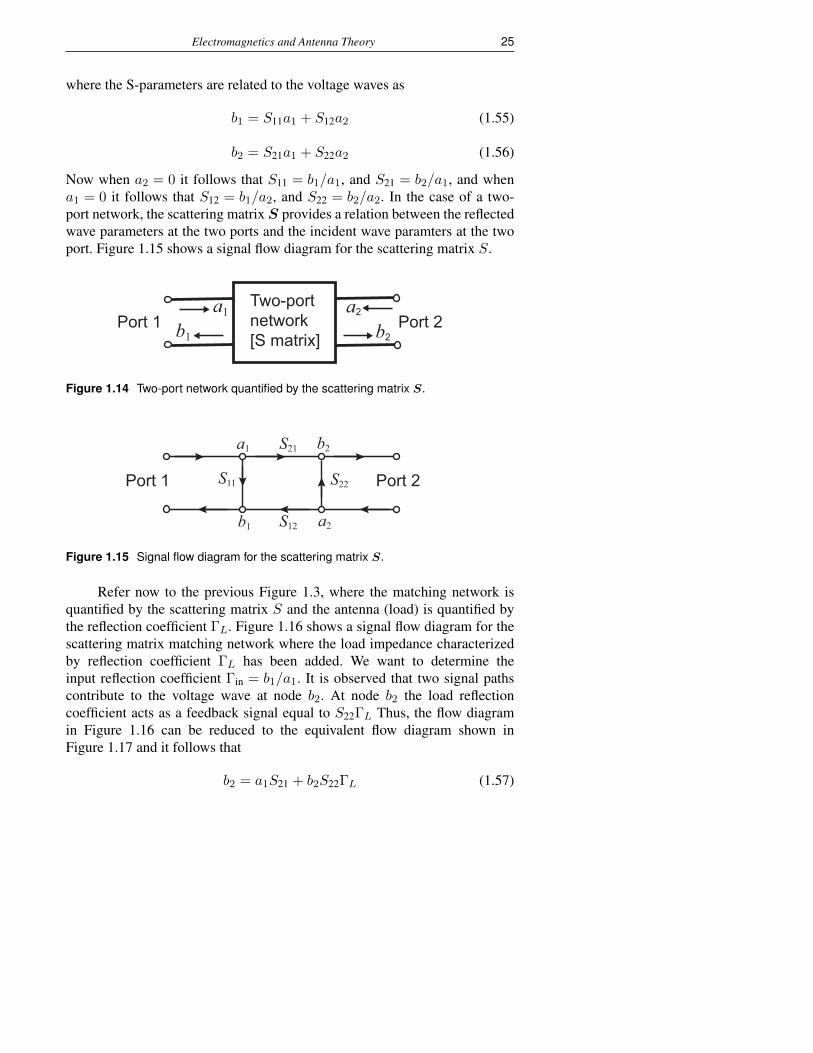
where the S-parameters are related to the voltage waves as
b1 = S11a1 + S12a2 (1.55)
b2 = S21a1 + S22a2 (1.56)
Now when a2 = 0 it follows that S11 = b1/a1, and S21 = b2/a1, and whena1 = 0 it follows that S12 = b1/a2, and S22 = b2/a2. In the case of a two-port network, the scattering matrix S provides a relation between the reflectedwave parameters at the two ports and the incident wave paramters at the twoport. Figure 1.15 shows a signal flow diagram for the scattering matrix S.
Two-portnetwork[S matrix]
Port 1 Port 2a1 a2
b1 b2
Figure 1.14 Two-port network quantified by the scattering matrix S.
S11
S12
Port 1 Port 2S22
S21a1
b1 a2
b2
Figure 1.15 Signal flow diagram for the scattering matrix S.
Refer now to the previous Figure 1.3, where the matching network isquantified by the scattering matrix S and the antenna (load) is quantified bythe reflection coefficient ΓL. Figure 1.16 shows a signal flow diagram for thescattering matrix matching network where the load impedance characterizedby reflection coefficient ΓL has been added. We want to determine theinput reflection coefficient Γin = b1/a1. It is observed that two signal pathscontribute to the voltage wave at node b2. At node b2 the load reflectioncoefficient acts as a feedback signal equal to S22ΓL Thus, the flow diagramin Figure 1.16 can be reduced to the equivalent flow diagram shown inFigure 1.17 and it follows that
b2 = a1S21 + b2S22ΓL (1.57)
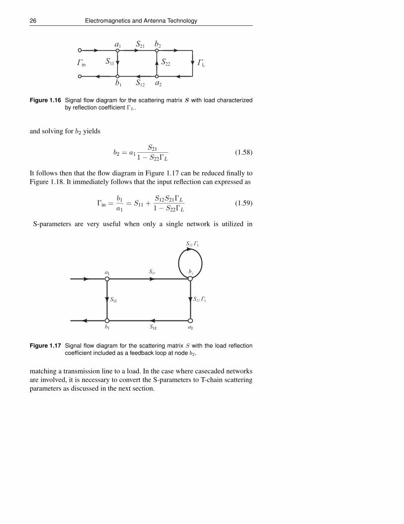
26 Electromagnetics and Antenna Technology
S11
S12
S22
S21a1
b1 a2
b2
ΓLΓin
Figure 1.16 Signal flow diagram for the scattering matrix S with load characterizedby reflection coefficient ΓL.
and solving for b2 yields
b2 = a1S21
1− S22ΓL(1.58)
It follows then that the flow diagram in Figure 1.17 can be reduced finally toFigure 1.18. It immediately follows that the input reflection can expressed as
Γin =b1a1
= S11 +S12S21ΓL1− S22ΓL
(1.59)
S-parameters are very useful when only a single network is utilized in
b2
a2
a1
b1 S12
S11
S21
S22 ΓL
S22 ΓL
Figure 1.17 Signal flow diagram for the scattering matrix S with the load reflectioncoefficient included as a feedback loop at node b2.
matching a transmission line to a load. In the case where casecaded networksare involved, it is necessary to convert the S-parameters to T-chain scatteringparameters as discussed in the next section.
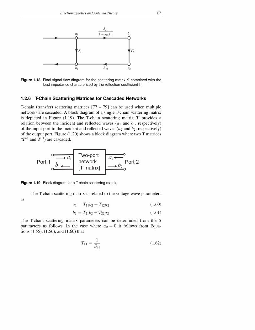
Electromagnetics and Antenna Theory 27
b2
a2
a1
b1 S12
S11
S21
1 – S22ΓL
ΓL
Figure 1.18 Final signal flow diagram for the scattering matrix S combined with theload impedance characterized by the reflection coefficient Γ.
1.2.6 T-Chain Scattering Matrices for Cascaded Networks
T-chain (transfer) scattering matrices [77 – 79] can be used when multiplenetworks are cascaded. A block diagram of a single T-chain scattering matrixis depicted in Figure (1.19). The T-chain scattering matrix T provides arelation between the incident and reflected waves (a1 and b1, respectively)of the input port to the incident and reflected waves (a2 and b2, respectively)of the output port. Figure (1.20) shows a block diagram where two T matrices(TA and TB) are cascaded.
Two-portnetwork[T matrix]
Port 1 Port 2a1 a2
b1 b2
Figure 1.19 Block diagram for a T-chain scattering matrix.
The T-chain scattering matrix is related to the voltage wave parametersas
a1 = T11b2 + T12a2 (1.60)
b1 = T21b2 + T22a2 (1.61)
The T-chain scattering matrix parameters can be determined from the Sparameters as follows. In the case where a2 = 0 it follows from Equa-tions (1.55), (1.56), and (1.60) that
T11 =1
S21(1.62)
28 Electromagnetics and Antenna Technology
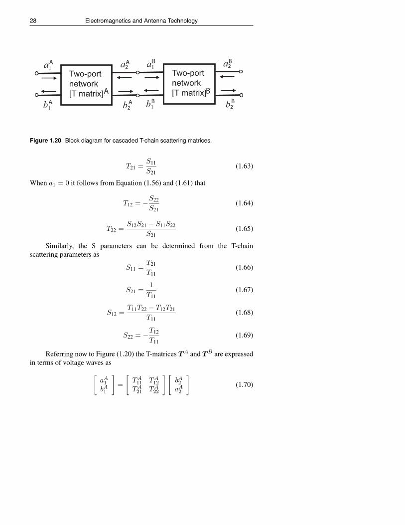
Two-portnetwork[T matrix]
a1 a2
b1 b2
A
A
AA
A
Two-portnetwork[T matrix]
a1 a2
b1 b2
B
B
BB
B
Figure 1.20 Block diagram for cascaded T-chain scattering matrices.
T21 =S11
S21(1.63)
When a1 = 0 it follows from Equation (1.56) and (1.61) that
T12 = −S22
S21(1.64)
T22 =S12S21 − S11S22
S21(1.65)
Similarly, the S parameters can be determined from the T-chainscattering parameters as
S11 =T21
T11(1.66)
S21 =1
T11(1.67)
S12 =T11T22 − T12T21
T11(1.68)
S22 = −T12
T11(1.69)
Referring now to Figure (1.20) the T-matrices TA and TB are expressedin terms of voltage waves as[
aA1bA1
]=
[TA11 TA12
TA21 TA22
] [bA2aA2
](1.70)
Electromagnetics and Antenna Theory 29
[aB1bB1
]=
[TB11 TB12
TB21 TB22
] [bB2aB2
](1.71)
but since [bA2aA2
]=
[aB1bB1
](1.72)
it follows that the cascaded T-chain matrices can be expressed as[aA1bA1
]=
[TA11 TA12
TA21 TA22
] [TB11 TB12
TB21 TB22
] [bB2aB2
](1.73)
Thus, the cascaded T-matrix product is given by
TC = TATB (1.74)
Once the cascaded T-matrix product TC has been computed, the S-parametersfor the cascaded network can then be determined by Equations (1.66) to(1.69).
1.3 Electromagnetic Radiation: Maxwell’s Equations
This section begins with a brief discussion of accelerated charges, time-varying currents, and photons, with the goal of providing a fundamentalunderstanding of the mechanisms of electromagnetic radiation as describedmathematically by Maxwell’s equations.
Electromagnetic waves are known to be generated by accelerated elec-tron charges or, equivalently, by time-varying currents [1-14]. For example,the time-varying vector current density J(t) with units of amperes/m2 at aparticular cross section of an electrically conducting antenna can be expressedin terms of the volume electric charge density ρ (coulombs/m3) and thevelocity v(t) (m/s) of the charge as
J(t) = ρv(t). (1.75)
Thus, the electric current density has units of coulombs per m2 per second.In Equation (1.75), the local charge density is related to the electron charge(denoted as qe) times the number of electrons (Ne) accelerated through thelocal cross section of the antenna, that is,
ρ = qeNe. (1.76)
30 Electromagnetics and Antenna Technology
Taking the derivative of J(t) with respect to time yields
dJ(t)
dt= ρ
dv(t)
dt= ρa(t) (1.77)
where dv(t)/dt = a(t) is the acceleration of the charge with units of m/s2.Thus, the units of the time derivative of the current density are coulombs permeters squared per second per second, and, as will be shown, radiation occurswhen the time derivative of the current density J is nonzero and equivalentlywhen the charge acceleration a is nonzero. The time derivative of the currentdensity and acceleration of charge are of interest in explaining the source ofthe electromagnetic radiation for antenna systems.
A complete characterization of electromagnetic fields can be determinedby means of Maxwell’s equations. However, in the process of generatingelectromagnetic waves, an intermediate process, referred to in the literature asphoton emission, occurs and ultimately produces the electromagnetic wave. Aphoton can be described as a discrete packet of electromagnetic radiation thatincludes X rays, visible light, and microwaves. The term ionizing radiationrefers to radiation that has enough energy to knock electrons out of atomsand includes X rays, protons, heavy ions, and neutrons that are generatedby accelerators. Nonionizing radiation includes visible light, ultraviolet (UV)radiation, infrared (IR) radiation, and microwaves. In the case of an antennareceiving an electromagnetic wave, photon absorption and scattering occurwith some probability that produces accelerated charges or, equivalently, time-varying currents on the antenna. Here, a brief discussion of the generationand reception of photons and electromagnetic waves is given. A completemathematical treatment of photon emission and photon absorption is beyondthe scope of this book, and the reader is referred to other sources mentionedin the paragraphs below. One situation in which photon/electron interactionis important is in determining the effect of electromagnetic waves on humantissues as a potential safety issue. When the electromagnetic wave frequencyis sufficiently high, as is the case for X-ray radiation, the energy in theelectromagnetic photons is large enough to break the atom-electron bondand knock out electrons causing damage to the DNA of tissue. Low-level(nonthermal) microwave energy does not contain sufficient photon energyto knock out electrons from tissue, but if the power density is sufficientlyhigh and is applied for a sufficient time interval, it is capable of heating anddamaging tissues [96, 97]. The interaction of microwave energy and a widerange of dielectric materials has been investigated in the literature [98].
For RF transmission, when a time-varying signal voltage (e.g., asinusoidal or pulsed waveform) on a transmission line is applied across theterminals of an antenna, electrons (negatively charged particles) distributed

Electromagnetics and Antenna Theory 31
across the metallic lattice portion of the antenna experience a time-varyingvector force, and they accelerate and generate a time-varying electric current.An electron has a negative electric charge equal to qe = −1.602× 10⁻¹⁹
coulombs and a rest mass of moe = 9.109× 10⁻³¹ kg. The RF-inducedacceleration of the electrons alters their vector momentum and energy state,which with some probability gives rise to the emission of RF photons,which can be described in a dual nature as particles or waves with zero restmass (mop = 0) and zero electric charge (qp = 0), as described by Cohen-Tannoudji [100, 101]. Each photon has an energy level E (equal to the changein energy level between the excited state and the ground state of an electron)as computed by
E = hf (1.78)
where h = 6.626× 10⁻³⁴J-s is Planck’s constant and f is the frequencyin cycles per second or Hertz (Hz). For example, the energy of a singlemicrowave photon packet at 300 MHz is computed and rounded as
E = (6.626× 10⁻³⁴J-s)(300× 106s−1) = 2× 10⁻²⁵J. (1.79)
Suppose an antenna is radiating 1 watt or 1 joule per second of microwavepower, then the number of 300 MHz microwave photons generated per secondis computed as
Nphotons per second =1J/s
2× 10⁻²⁵J/photon= 5× 1024. (1.80)
Microwave photons are polarized according to the design of the antenna,which can be linear, circular, or elliptically polarized. In free space, RFphotons travel at the speed of light, and they have an energy-momentum vectorp with amplitude equal to
p =h
λ=hf
c(1.81)
where λ = c/f is the wavelength of the photon in free space. It should benoted that the energy-momentum vector p has units of J-s/m.
As microwave power is continuously pumped into the antenna terminals,RF photons are continuously generated and radiated outward from thetransmitting antenna. When a sufficient amount and spatial distribution ofphotons are generated from the radiating antenna, a propagating wavefront,described by an electromagnetic field, is created. Electromagnetic fields (andphotons) are characterized by Maxwell’s equations, and these fields travel atthe speed of light in vacuum and slower than the speed of light in a dielectricmedium.
32 Electromagnetics and Antenna Technology
The characteristics of the electromagnetic-field wavefront, such asthe spatial distribution of amplitude and phase, signal bandwidth, powerdensity, and polarization, depend on the design of the antenna and thecharacteristics of the transmitting source. The radiating field will produce aforce on any electrical charges that it may encounter. The total time-varyingelectromagnetic force vector F (r, t) at vector position r and time t appliedto an electric charge q is given by the Lorentz force equation as described byJackson [102, p. 3]:
F (r, t) = qE(r, t) + qv(r, t)×B(r, t) (1.82)
where q is the charge of the particle (in this case an electron),E is the electric-field vector, v is the vector velocity of the charged particle,B is the magneticflux density, and the symbol × means vector cross product. Such chargeswill exist, for example, as electrons in a distant metallic receive antennafor communications or within a metallic or other scattering target in a radarapplication.
For RF signal reception, when a time-varying electromagnetic field isincident on a metallic antenna, the electrons in the metal experience a time-varying force, as computed by the Lorentz force equation, which acceleratesthem according to the classical equation
F (t) = ma(t) (1.83)
or
a(t) =F (t)
m(1.84)
where a(t) is the acceleration as a function of time and m is the mass ofthe particle. Equivalently, the photon particles in the incident electromagneticfield are absorbed with some probability by the electrons in the metal, alteringthe electron momentum and causing acceleration of the electrons. (Theinteraction of the moving, drifting electrons in the metal is a complex process,but here we only care about the net effect.) For low velocities (v << c), usingEquation (1.82), the force on the electrons in the metal can be approximatedby F (t) = qE(t), and in the case of a sinusoidally varying electric fieldfrom Equation (1.84), the force and charge acceleration are time varying ina sinusoidal fashion as well.
The acceleration of the negatively charged electrons induces a time-varying electric current in the metallic antenna, which produces a signalvoltage across the antenna terminals connected to the transmission line thatis connected to a receiver. The time variation of the electric current in thereceive antenna tends to be matched to the time variation of the incident field,depending on the design of the antenna.
Electromagnetics and Antenna Theory 33
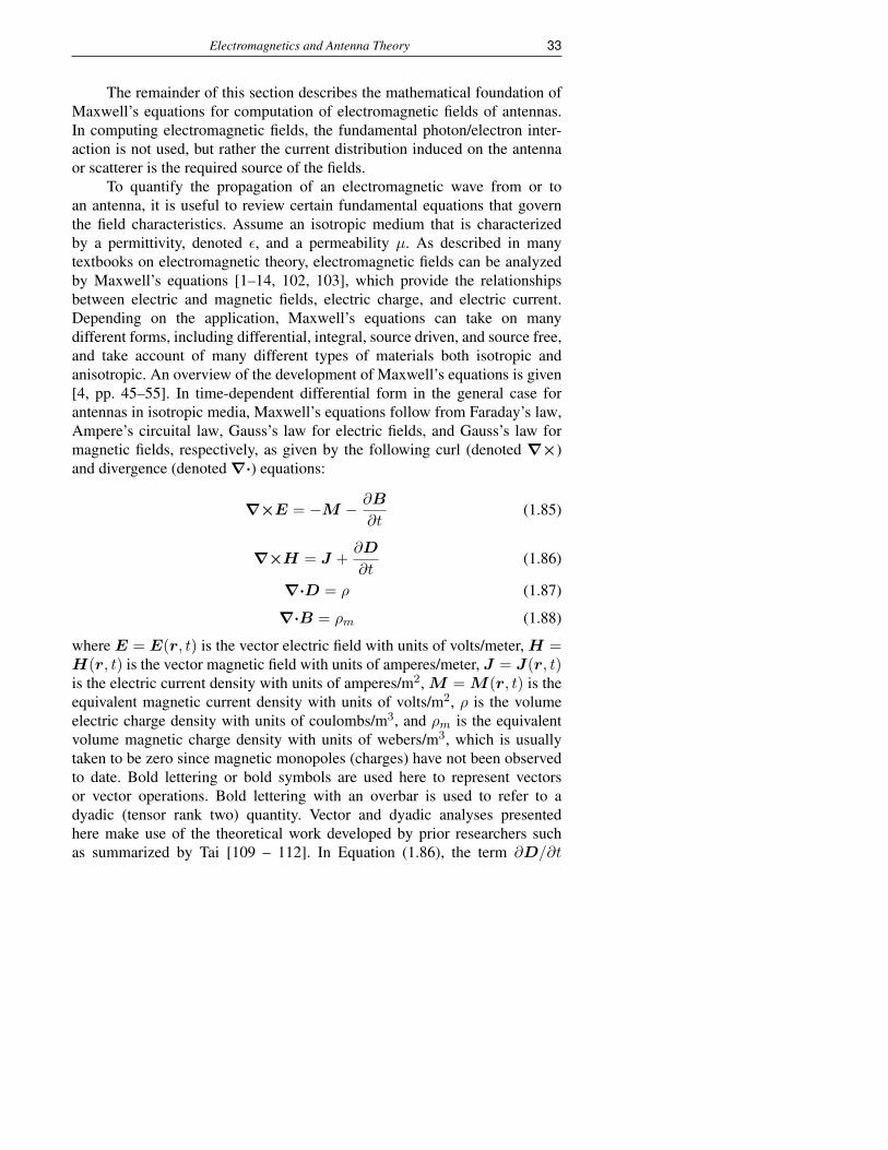
The remainder of this section describes the mathematical foundation ofMaxwell’s equations for computation of electromagnetic fields of antennas.In computing electromagnetic fields, the fundamental photon/electron inter-action is not used, but rather the current distribution induced on the antennaor scatterer is the required source of the fields.
To quantify the propagation of an electromagnetic wave from or toan antenna, it is useful to review certain fundamental equations that governthe field characteristics. Assume an isotropic medium that is characterizedby a permittivity, denoted ε, and a permeability µ. As described in manytextbooks on electromagnetic theory, electromagnetic fields can be analyzedby Maxwell’s equations [1–14, 102, 103], which provide the relationshipsbetween electric and magnetic fields, electric charge, and electric current.Depending on the application, Maxwell’s equations can take on manydifferent forms, including differential, integral, source driven, and source free,and take account of many different types of materials both isotropic andanisotropic. An overview of the development of Maxwell’s equations is given[4, pp. 45–55]. In time-dependent differential form in the general case forantennas in isotropic media, Maxwell’s equations follow from Faraday’s law,Ampere’s circuital law, Gauss’s law for electric fields, and Gauss’s law formagnetic fields, respectively, as given by the following curl (denoted ∇×)and divergence (denoted∇·) equations:
∇×E = −M − ∂B
∂t(1.85)
∇×H = J +∂D
∂t(1.86)
∇·D = ρ (1.87)
∇·B = ρm (1.88)
where E = E(r, t) is the vector electric field with units of volts/meter, H =H(r, t) is the vector magnetic field with units of amperes/meter, J = J(r, t)is the electric current density with units of amperes/m2, M = M(r, t) is theequivalent magnetic current density with units of volts/m2, ρ is the volumeelectric charge density with units of coulombs/m3, and ρm is the equivalentvolume magnetic charge density with units of webers/m3, which is usuallytaken to be zero since magnetic monopoles (charges) have not been observedto date. Bold lettering or bold symbols are used here to represent vectorsor vector operations. Bold lettering with an overbar is used to refer to adyadic (tensor rank two) quantity. Vector and dyadic analyses presentedhere make use of the theoretical work developed by prior researchers suchas summarized by Tai [109 – 112]. In Equation (1.86), the term ∂D/∂t

34 Electromagnetics and Antenna Technology
was introduced as a displacement current density by Maxwell. The previousMaxwell equations take into account the general properties of the linearisotropic material, radiating sources, and fields, all of which can have bothspatial and time dependence. The inclusion (for mathematical convenience) ofthe equivalent magnetic current density M and equivalent volume magneticcharge density ρm allows for analysis of aperture fields and other generalelectromagnetics problems requiring these equivalent quantities. In the priorform of the Maxwell’s equations, the time dependence of the electromagneticfields is arbitrary. For arbitrary antenna geometries, this time-dependent formof the Maxwell equations can be solved via numerical methods such asthe finite difference time domain technique. An overview of computationalmethods for solving Maxwell’s equations for the electromagnetic fields isgiven for example in [2]. For the case in which the material properties arelinear, isotropic, and nondispersive, the following constitutive relations hold:
D(r, t) = εE(r, t) (1.89)
where D is the vector electric flux density with units of coulombs/m2, and εis the permittivity of the material
B(r, t) = µH(r, t) (1.90)
where B is the vector magnetic flux density with units of webers/m2, and µis the permeability of the material. Equations (1.89) and (1.90) are referred toas the constitutive relations, and in this isotropic case, D is parallel to E andB is parallel to H . In general, the material properties ε and µ are frequencydependent.
In the case in which the material is anisotropic, the constitutive relationsare expressed in terms of the material dyadic (tensor) quantities ε and µ toconvert the vector fields to vector flux densities as
D(r, t) = ε·E(r, t) (1.91)
B(r, t) = µ·H(r, t) (1.92)
where the overbar is used to indicate a dyadic quantity (refer to Section 1.6for a detailed discussion of dyadics), and the symbol · means dot product. Forthe anisotropic case, the vector directions of the vector flux densities D andB can be different from the vector directions of the vector fields E and H ,respectively.
In spherical coordinates, with A = Arr +Aθθ +Aφφ, the curl oper-ation ∇×A is given in terms of the unit vectors r, θ, φ in convenient
Electromagnetics and Antenna Theory 35
determinant form as
∇×A =1
r2 sin θ
∣∣∣∣∣∣∣r rθ r sin θφ∂∂r
∂∂θ
∂∂φ
Ar rAθ r sin θAφ
∣∣∣∣∣∣∣ . (1.93)
Performing the determinant operation in Equation (1.93), the curl operation inexpanded form is then given by
∇×A = rr sin θ
[∂∂θ (Aφ sin θ)− ∂Aθ
∂φ
]+
ˆθr
[1
sin θ∂Ar∂φ −
∂∂r (rAφ)
]+
ˆφr
[∂∂r (rAθ)− ∂Ar
∂θ
].
(1.94)The divergence operation∇·A is given by
∇·A =1
r2
∂
∂r(r2Ar) +
1
r sin θ
∂
∂θ(Aθ sin θ) +
1
r sin θ
∂
∂φ(Aφ). (1.95)
Additionally, note that the vector cross product in spherical coordinates isgiven by
A×B =
r θ φAr Aθ AφBr Bθ Bφ
. (1.96)
Substituting Equations (1.89) and (1.90) into Equations (1.85) and(1.86), respectively, yields an alternate representation of Maxwell’s equations:
∇×E = −M − µ∂H∂t
(1.97)
∇×H = J + ε∂E
∂t(1.98)
∇·D = ρ (1.99)
∇·B = ρm. (1.100)
An equation for expressing the continuity of electrical charge canbe derived by taking the divergence of Maxwell’s curl equation for themagnetic field, (∇·∇×H), and applying Gauss’s law for electric fields(Equation (1.99)), and using the property that the divergence of the curl ofany vector is zero, with the result
∇·J(r, t) = −∂ρ(r, t)
∂t. (1.101)

36 Electromagnetics and Antenna Technology
The continuity equation given by Equation (1.101) indicates that thedivergence of the electric current density J depends on the time rate of changeof the charge density. Similarly, an equation for expressing the continuityof equivalent magnetic charge can be derived by taking the divergence ofMaxwell’s curl equation for the electric field, applying Gauss’s law formagnetic fields, and using the property that the divergence of the curl of anyvector is zero, with the result
∇·M(r, t) = −∂ρm(r, t)
∂t. (1.102)
The continuity equation given by Equation (1.102) indicates that thedivergence of the equivalent magnetic current densityM depends on the timerate of change of the equivalent magnetic charge density ρm.
The electric current density J in Equation (1.98) can be composed of asource current J source and a conduction current Jc as
J = J source + Jc. (1.103)
For a conducting medium with electrical conductivity σ having units ofsiemens/meter (amperes per volt-meter), the conducting current density Jcand electric field E are related as
Jc = σE, (1.104)
which is Ohm’s law for conducting current density. Note that electricalconductivity is equal to the reciprocal of electrical resistivity. In free space,it should be noted that σ = 0.
Similarly, the equivalent magnetic current densityM in Equation (1.97)can be composed of an equivalent magnetic source current M source and anequivalent magnetic conduction current expressed as
M c = σmH (1.105)
where σm is the magnetic conductivity that has units of ohms per meter.Thus, in the case of a lossy dielectric material, the electric current
density can be expressed as
J = J source + σE. (1.106)
Similarly, in the case of a lossy magnetic material, the magnetic currentdensity can be written as
M = M source + σmH. (1.107)
Electromagnetics and Antenna Theory 37
In summary, the source currents J source and M source produce the electromag-netic fields, which then induce a corresponding conduction current density.
Substituting Equations (1.106) and (1.107) into Maxwell’s curl equa-tions given by Equations (1.97) and (1.98) yields an alternate form ofMaxwell’s equations as
∇×E = −M source − σmH − µ∂H
∂t(1.108)
∇×H = J source + σE + ε∂E
∂t(1.109)
∇·D = ρ (1.110)
∇·B = ρm. (1.111)
The instantaneous electric and magnetic fields, as a function of spatialposition (x, y, z) or position vector (r) and time t, are real functions, andfor the time-harmonic case, they are sinusoidal (or cosinusoidal) and can beexpressed as
E(r, t) = |E(r)| cos(ωt+ ψ(r)) = |E(r)| cos(ωt− kr) (1.112)
H(r, t) = |H(r)| cos(ωt+ ψ(r)) = |H(r)| cos(ωt− kr) (1.113)
where ψ(r) = −kr is the spatial phase variation of the electric and magneticfields, with k = 2π/λ = ω
√µε the wavenumber, and ω = 2πf is the radian
frequency, where f is the frequency. The time-harmonic fields can be extendedto most waveforms by utilizing standard Fourier transform techniques.Equivalently, the instantaneous electric and magnetic fields can be written in amore convenient exponential form in terms of the non-time-varying complexelectric and magnetic fields E(r) andH(r) as
E(r, t) = Re[E(r)ejωt] (1.114)
H(r, t) = Re[H(r)ejωt] (1.115)
where Re[·] indicates the real part. Note that the ejωt convention used herethroughout is common to the electrical engineering convention; however, incases for which the e−iωt convention would be used, the equations presentedhere can be converted by simply interchanging jωt with −iωt. Similarly,the instantaneous electric current density J and equivalent magnetic currentdensityM can be written as
J(r, t) = Re[J(r)ejωt] (1.116)

38 Electromagnetics and Antenna Technology
M(r, t) = Re[M(r)ejωt]. (1.117)
The time-dependent fields can also be expressed in terms of themagnitude and phase of the fields as
E(r, t) = Re[|E(r)|ej(ωt+ψ(r))] (1.118)
H(r, t) = Re[|H(r)|ej(ωt+ψ(r))]. (1.119)
If the Re[·] operation in Equations (1.118) and (1.119) is dropped and the ejωt
factor is suppressed, then the following phasor designations for the electricand magnetic fields can also be used:
E(r) = |E(r)|ejψ(r) (1.120)
H(r) = |H(r)|ejψ(r). (1.121)
In Equations (1.120) and (1.121), the magnitudes |E(r)| and |H(r)|represent the envelope of the electric and magnetic fields, respectively.
In an electrically conducting medium, the electric flux densityD is givenby
D(r, t) = ε′E(r, t) (1.122)
where ε′ is the real part of the complex permittivity of the medium. Similarly,in a magnetically conducting medium, the magnetic flux density B is givenby
B(r, t) = µ′H(r, t) (1.123)
where µ′ is the real part of the complex permeability of the medium.With the prior relations, it is now possible to convert Maxwell’s
equations to a time-harmonic form as follows. This form of the Maxwellequations is particularly amenable to solution via numerical methods suchas the method of moments. Substituting Equations (1.114), (1.115), (1.122),(1.123), and (1.116) into Equations (1.97) and (1.98) yields
∇×Re[E(r)ejωt] = −Re[M(r)ejωt]− ∂
∂tRe[µ′H(r)ejωt] (1.124)
∇×Re[H(r)ejωt] = Re[J(r)ejωt] +∂
∂tRe[ε′E(r)ejωt] (1.125)
and computing the partial derivatives, and noting that the real operationcommutes with the partial derivative operation, yields
Re∇×[E(r)ejωt] = −Re[M(r)ejωt]− Re[jωµ′H(r)ejωt] (1.126)
Electromagnetics and Antenna Theory 39
Re∇×[H(r)ejωt] = Re[J(r)ejωt] + Re[jωε′E(r)ejωt]. (1.127)
The previous two equations can be simplified by dropping the real (Re)operation and suppressing the exponential function ejωt that are common toall terms, with the result for Maxwell’s equations in time-harmonic (frequencydomain) form
∇×E = −M − jωµ′H (1.128)
∇×H = J + jωε′E (1.129)
∇·D = ρ (1.130)
∇·B = ρm. (1.131)
In the prior Maxwell’s equations, the real part of the complex perme-ability can be expressed as
µ′ = µ′rµo (1.132)
where µ′r is the relative permeability and µo is the permeability of free space.The real part of the complex permittivity is expressed as
ε′ = ε′rεo (1.133)
where ε′r is the dielectric constant (relative permittivity) and εo is thepermittivity of free space. In free space, the speed of light c (also the speed ofelectromagnetic wave propagation) is related to εo and µo as
c =1
√µoεo
(1.134)
and has a measured value of approximately 2.99792458× 10⁸ m/s ≈ 3.0×10⁸ m/s. The value of εo can be measured by an experiment involvingCoulomb’s force law for two charges separated by a distance [4, p. 61]. Theestablished value for the permittivity of free space is εo = 1
36π × 10−9 =8.8542× 10⁻¹² farads/meter (farads have units of amperes-seconds/volts).The established value for the permeability of free space is µo = 4π × 10−7 =1.257× 10⁻⁶ henries/meter (henries have units of volts-seconds/ampere).
To determine the speed of electromagnetic wave propagation, considernow Equations (1.112) and (1.113) and follow a constant phase point alongthe electromagnetic wavefront. Then taking the derivative with respect to timeof the argument of the cosine function set equal to a constant yields
d
dt(ωt− kr) = ω − kdr
dt= 0 (1.135)

40 Electromagnetics and Antenna Technology
or in free spacedr
dt=ω
k=
ω
ω√µoεo
= c, (1.136)
which shows that the time-harmonic electromagnetic fields travel at the speedof light.
For an electrically conducting medium, the electrical conducting currentdensity Jc and electric field E are related by Equation (1.104). When asource J source is present, substituting Equations (1.103) and (1.104) intoEquation (1.129) yields
∇×H = J source + (σ + jωε′)E. (1.137)
In Equation (1.137), the quantity (σ + jωε′) can be expressed as a complexelectrical conductivity σc as
σ + jωε′ = σ′ + jσ′′ = σc (1.138)
where it is observed that the real part of σc is σ′ = σ and the imaginary partis σ′′ = ωε′.
The electrical conductivity σ of the dielectric medium can be expressedin terms of the imaginary component (denoted ε′′) of the complex permittivityas
σ = ωε′′ = ωεoε′′r (1.139)
where ε′′r is the relative imaginary component of the complex permittivity.Thus, using Equations (1.133) and (1.139), it follows that Equation (1.137)can be expressed as
∇×H = J source + (jωεoε′r + ωεoε
′′r)E, (1.140)
which can be written in an alternate form (by factoring the quantity jωεo) as
∇×H = J source + jωεo(ε′r − jε′′r)E. (1.141)
In Equation (1.141), the complex permittivity of the conducting medium canbe expressed in terms of real and imaginary components as
εc = ε′ − jε′′ = εo(ε′r − jε′′r). (1.142)
Similarly, the complex permeability can be defined in terms of real andimaginary components as
µc = µ′ − jµ′′ = µo(µ′r − jµ′′r). (1.143)

Electromagnetics and Antenna Theory 41
Thus, Equation (1.141) can be written in a simplified form in terms of thecomplex permittivity given by Equation (1.142) as
∇×H = J source + jωεcE. (1.144)
By using the above mathematical development and a similar develop-ment for equivalent magnetic current, an explicit representation of Maxwell’sequations in time-harmonic (frequency domain) form can be written in termsof source currents as
∇×E = −M source − jωµcH (1.145)
∇×H = J source + jωεcE (1.146)
∇·D = ρ (1.147)
∇·B = ρm. (1.148)
In the above form of Maxwell’s equations, the electric conduction current haseffectively been folded into the complex permittivity quantity.
By comparing the Maxwell curl of H equations given by Equa-tions (1.137) and (1.146), the following relations can be determined:
jωεc = σ + jωε′ (1.149)
and solving for εc yields
εc = ε′ − j σω
= ε′ − jε′′. (1.150)
Thus,ε′′ =
σ
ω(1.151)
and it follows from Equation (1.142) that
εc = εo(ε′r − j
σ
ωεo), (1.152)
which can be rewritten as
εc = εoε′r(1− j
σ
ωεoε′r) (1.153)
or asεc = εoε
′r(1− j
σ
ωε′). (1.154)
Next, defining the loss tangent as
tan δ =σ
ωε′, (1.155)
the complex permittivity can be expressed as
εc = εoε′r(1− j tan δ). (1.156)

42 Electromagnetics and Antenna Technology
1.4 Fields from Time-Varying Electric and MagneticCurrent Sources
In this section, Maxwell’s equations (described in the previous section)are used to formulate the radiated electromagnetic fields from time-varyingelectric and magnetic current sources. A detailed derivation is given for thecase of electric current sources, and the result is simply stated for magneticcurrent sources.
Maxwell’s equations as given by Equations (1.97–1.100) can beexpressed in the time domain in terms of the current densities J andM as
∇×E(r, t) = −M(r, t)− µ∂H(r, t)
∂t(1.157)
∇×H(r, t) = J(r, t) + ε∂E(r, t)
∂t(1.158)
∇·D(r, t) = ρ (1.159)
∇·B(r, t) = ρm. (1.160)
It was mentioned at the start of the previous section that the source ofelectromagnetic radiation is the time-varying current, which is equal to theacceleration of charges. To demonstrate this fact, the following derivation canbe made by using Maxwell’s curl equations and a vector identity. Starting withthe curl of Maxwell’s curl ofE equation with the equivalent magnetic currentsource equal to zero, that is, M source = 0 and the equivalent magnetic chargeequal to zero (ρm = 0), and assuming free space, that is, µ = µo, ε = εo,σ = 0, and Jc = 0 so J = J source,
∇×∇×E = −µo∂
∂t∇×H (1.161)
and substituting Maxwell’s curl ofH equation expressed as
∇×H = J + εo∂E
∂t(1.162)
yields
∇×∇×E − µoεo∂2E
∂t2= −µo
∂
∂tJ . (1.163)
Now use the vector identity
∇×∇×E =∇(∇·E)−∇2E (1.164)
Electromagnetics and Antenna Theory 43
where∇2 =∇·∇ (1.165)
is the Laplacian operator, such that Equation (1.163) becomes
∇(∇·E)−∇2E − µoεo∂2E
∂t2= −µo
∂
∂tJ . (1.166)
It should be noted that the quantity ∇2E =∇·∇E yields a vector. Thequantity∇E yields a dyadic (tensor of order two), and then taking the diver-gence of the dyadic yields a vector. The left-hand side of Equation (1.166)contains expressions involving the electric field E and the right-hand sideis a function of the derivative of the time-varying current density J . Thus,Equation (1.166) is inhomogeneous and it explicitly shows that the timederivative of the electric current density J(t) is a source of electromagneticradiation. Substituting Equation (1.77) in Equation (1.166) yields
∇(∇·E)−∇2E − µoεo∂2E
∂t2= −µoρa, (1.167)
which explicitly shows that the charge ρ with acceleration a is a sourceof electromagnetic radiation, as desired. Furthermore, in free space, usingEquation (1.134) in Equation (1.167) yields the following inhomogeneousequation in terms of the speed of light with the accelerated charge as thedriving function for the operations on the electric field:
∇(∇·E)−∇2E − 1
c2
∂2E
∂t2= −µoρa. (1.168)
When both ρ = 0 and J = 0, that is, there are no local sources,Equations (1.166) to (1.168) reduce to the homogeneous wave equation formas
∇2E − 1
c2
∂2E
∂t2= 0, (1.169)
and similarly it can be shown that
∇2H − 1
c2
∂2H
∂t2= 0. (1.170)
Equations (1.169) and (1.170) indicate that in free space the electromagneticfield exists and is self-sustaining and propagating at the speed of light in theabsence of local driving sources.
While Equations (1.166) to (1.168) indicate a source of the electromag-netic radiation, to compute the electromagnetic fields from the electric current
44 Electromagnetics and Antenna Technology
density J for a practical antenna, it is necessary to determine an expressionfor E in terms of J .
Consider now, in the frequency domain, the derivation of the electro-magnetic fields caused by an electric current source J radiating in an infinitespace described by the complex parameters µ = µc and ε = εc (note: althoughrepresented here as scalar quantities, µ and ε can also be dyadic [tensor]quantities). There are two ways to arrive at the desired expression for E interms of a volume integral involving J . One way starts with the traditionalmagnetic vector potential approach, as derived in the time-harmonic form[2], and with this approach, the scalar Green’s function for isotropic mediais used. The other approach is to use the dyadic Green’s function approachas described by Tai [109] and Kong [3]. The Green’s function characterizesthe response to a point source and essentially allows the current densitydistribution to be integrated in such a way as to determine the electromagneticfield distribution in the surrounding space. Both approaches using the scalarGreen’s function and the dyadic Green’s function are described, respectively,in the next two sections.
1.4.1 Magnetic Vector Potential and the Scalar Green’s Function
Starting with the Maxwell divergence equation for the time-harmonicmagnetic field (Equation [1.131]) with the equivalent magnetic charge densityequal to zero yields
∇·B =∇·µH = 0, (1.171)
that is,∇·H = 0. (1.172)
Since the divergence of the vector magnetic field is zero, the vector magneticfield has only circulation and is called a solenoidal field, which can beexpressed in terms of the curl of another function by a vector identity. Now,define the magnetic flux density B in terms of the curl of a magnetic vectorpotential functionA as
B = µH =∇×A. (1.173)
Thus, the magnetic fieldH in terms ofA is just
H =1
µ∇×A. (1.174)
Substituting this result in Maxwell’s curl of E Equation (1.128) yields
∇×E = −jωµH = −jω∇×A, (1.175)

Electromagnetics and Antenna Theory 45
which can be rewritten as
∇× [E + jωA] = 0. (1.176)
Making use of the general vector identity
∇×∇Φ = 0 (1.177)
where Φ is defined as the electric scalar potential, allows Equation (1.176) tobe written as
∇× [E + jωA] = −∇×∇Φ (1.178)
or asE + jωA = −∇Φ, (1.179)
and solving for E asE = −jωA−∇Φ. (1.180)
Now use the vector identity
∇×∇×A =∇(∇·A)−∇2A (1.181)
such that from Equation (1.173)
∇×(µH) =∇(∇·A)−∇2A (1.182)
and for a homogeneous medium
µ∇×H =∇(∇·A)−∇2A. (1.183)
Now using the Maxwell curl equation for the magnetic field, that is,
∇×H = J + jωεE, (1.184)
Equation (1.183) can now be written as
µJ + jωµεE =∇(∇·A)−∇2A. (1.185)
Substituting Equation (1.180) in Equation (1.185) yields
∇2A+ ω2µεA = −µJ +∇(∇·A+ jωµεΦ). (1.186)
Next, applying the divergence operation on the electric field vector inEquation (1.180) as∇·E and using Maxwell’s equation∇·E = ρ/ε yields
∇2Φ + jω∇·A = −ρ/ε. (1.187)
46 Electromagnetics and Antenna Technology
In order to uncouple, simplify, and produce a wave-equation form ofEquations (1.186) and (1.187), the Lorenz condition [102, p. 240] can beinvoked, that is,
∇·A = −jωµεΦ. (1.188)
It should be noted that the Lorenz condition is consistent with the conservationof electric current and charge density as in the continuity equation fromEquation (1.101) expressed in time-harmonic form as (see the discussionfollowing Equation [1.201])
∇·J = −jωµρ. (1.189)
Substituting the Lorenz condition (Equation [1.188]) in Equation (1.186)yields
∇2A(r) + ω2µεA(r) = −µJ(r), (1.190)
which is an inhomogeneous vector wave equation. Similarly, it follows thatsubstituting Equation (1.188) in Equation (1.187) yields
∇2Φ + ω2µεΦ = −ρ/ε, (1.191)
which is an inhomogeneous scalar wave equation. Again by using the Lorenzcondition given by Equation (1.188), Equation (1.180) becomes
E = −jωA− j
ωµε∇(∇·A). (1.192)
Equation (1.192) is an exact relation between the vector electric field E andthe magnetic vector potential A and applies in the near field and far field of aradiating source. Thus, to determine the vector electric fieldE, it is necessaryto determine the magnetic vector potentialA.
Consider now Figure 1.6, which shows the coordinate system for aradiating source and field observation point. To solve the inhomogeneousequation given by Equation (1.190), the Green’s function method is used[113]. Let Lop be a linear differential operator such that
Lopy(x) = f(x). (1.193)
It is desired to determine the Green’s function G(x, x′) that is given by thesolution to
LopG(x, x′) = δ(x− x′) (1.194)
where δ is the delta function with δ(0) = 1 and δ is equal to zero otherwise,and boundary conditions must be satisfied. A solution for y(x) is then
y(x) =
∫G(x, x′)f(x′) dx′, (1.195)

Electromagnetics and Antenna Theory 47
which follows since
Lopy(x) =
∫LopG(x, x′)f(x′) dx′ =
∫δ(x− x′)f(x′) dx′ = f(x)
(1.196)where it is noted that δ(x− x′) acts as a sampling function andLop was movedinside the integral since this operator depends only on unprimed coordinates.Assume that the vector electric current source J is a function of the primedcoordinates (x′, y′, z′) and the position vectorR = r − r′ is a function of theobservation position (x, y, z) and the source coordinates. Then it follows fromEquation (1.195), which applies to each vector component in homogeneousspace solution of Equation (1.190) is
A(r) = µ
∫VJ(r′)
e−jk|r−r′|
4π|r − r′|dv′ (1.197)
wherek = ω
√µε (1.198)
is the wavenumber. Thus, in homogeneous space, the magnetic vectorpotential A is collinear with the source current J , which allows the use ofthe scalar Green’s function method to solve Equation (1.190). The magneticvector potential is also commonly expressed as
A(r) = µ
∫VJ(r′)g(r, r′) dv′. (1.199)
φ'
θ'
θ
φ
z
x
y
(x,y,z)
rrʹ
r–rʹ(x , y , zʹ)
Figure 1.21 Coordinate system for radiating source at r′ and field observation pointat r.
48 Electromagnetics and Antenna Technology
In Equation (1.199), the quantity
g(r, r′) =e−jk|r−r
′|
4π|r − r′|(1.200)
is referred to as the scalar Green’s function solution to the vector waveequation (Equation [1.190]), which is derived later in section 1.6.2 (startingwith Equation [1.311]). By solving Equation (1.191) using the Green’sfunction method, it can be shown that the electric scalar potential Φ is givenby
Φ(r) =1
ε
∫Vρ(r′)g(r, r′) dv′. (1.201)
Note that by substituting Equations (1.199) and (1.201) into the Lorenzcondition given by Equation (1.188), it is clear that the continuity equation(Equation [1.189]) is satisfied when multiplied by the scalar Green’s functionand integrated over a volume.
Using equation(1.197), Equation (1.192) can be written as
E = −jωµ∫VJ(r′)g(r, r′) dv′ − j
ωε∇[∇·∫VJ(r′)g(r, r′) dv′
](1.202)
or as
E = −jωµ∫VJ(r′)
e−jk|r−r′|
4π|r − r′|dv′ − j
ωε∇[∇·∫VJ(r′)
e−jk|r−r′|
4π|r − r′|dv′],
(1.203)which can be reduced to the following integral form
E = −jωµ[∫
VJ(r′)
e−jk|r−r′|
4π|r − r′|dv′ +
1
k2∇[∇·∫VJ(r′)
e−jk|r−r′|
4π|r − r′|dv′]]
(1.204)where k2 = ω2µε. Equation (1.204) can be expressed in a simplified form byusing a dyadic notation (discussed in Section 1.6.2) with I the identity dyadic(refer to Equation [1.242]):
E(r) = −jωµ[I +1
k2∇∇]·
∫VJ(r′)
e−jk|r−r′|
4π|r − r′|dv′, (1.205)
which is a general form of the electric field caused by an electric currentsource J .
A similar wave equation can be derived in terms of the electric vectorpotential F and the magnetic current densityM as
∇2F + ω2µεF = −εM (1.206)

Electromagnetics and Antenna Theory 49
and for the magnetic fieldH in terms of F as
H = −jωF − j
ωµε∇(∇·F ). (1.207)
The solution for F in terms ofM is given by
F (r) = ε
∫VM(r′)
e−jk|r−r′|
4π|r − r′|dv′. (1.208)
The fields radiated by an antenna are in general spherical waves. In thefar field, the spherical waves more closely resemble planar (plane) waves. Thefar-field range distance R from an antenna is typically computed as
R = 2D2/λ (1.209)
whereD is the antenna diameter and λ is the wavelength. In the far field, usingspherical coordinates, it can be shown (see Equation [1.279]) that only the firstterm in Equation (1.192) involving the θ and φ components is significant;thus,
EFF = −jω(Aθθ +Aφφ
). (1.210)
In the far zone in spherical coordinates, the radial component of theelectric and magnetic fields is zero, and the far-zone magnetic field can becomputed from the electric field in free space as (see Equation [1.281])
HFF =r×EFF
ηo(1.211)
where ηo is the wave impedance of free space as given by
ηo =
√µoεo. (1.212)
Similarly, it can be shown that the far-zone magnetic field HFF can becomputed from the electric vector potential F , for example, in sphericalcoordinates, as
HFF = −jω(Fθθ + Fφφ
)(1.213)
from which the far-zone electric field can be computed as
EFF = −ηor×HFF. (1.214)

50 Electromagnetics and Antenna Technology
Once the current density and field quantities have been determined, toconvert between frequency and time domains, the Fourier transform pairs canbe applied, for example, for J and E, as
J(r, ω) =
∫ ∞−∞
J(r, t)e−jωtdt (1.215)
J(r, t) =1
2π
∫ ∞−∞
J(r, ω)ejωtdω (1.216)
E(r, ω) =
∫ ∞−∞
E(r, t)e−jωtdt (1.217)
E(r, t) =1
2π
∫ ∞−∞
E(r, ω)ejωtdω. (1.218)
1.4.2 Dyadic Green’s Function
It was mentioned earlier in Section 1.6.1 that a direct dyadic relationshipbetween the source current and electric field can be determined. To see thisfact, Equations (1.192) and (1.197) can be combined and re-expressed byusing a dyadic notation as was given in Equation (1.205). In this section, thedyadic Green’s function is derived. Some background on vector and dyadicrelations is necessary to derive the desired expression. Given two vectors, Uand V , their dot product is expressed as U ·V , which is also referred to as aninner product. The inner product is equal to the product of a row vector UT
(U transpose) and a column vector V , which yields a scalar. Thus, U ·V =UTV is a scalar quantity. The dyadic D = UV is an outer product of twovectors and is the product of a column vector and a row vector, that is, UVis interpreted as UV T . Thus, D·C = UV ·C = U(V TC), that is, a vectorweighted by a scalar. Let the unit vectors in a given coordinate system, suchas Cartesian, cylindrical, or spherical, be expressed as e1, e2, e3. Now, let thetwo vectors U and V be represented in terms of the unit vectors as
U = U1e1 + U2e2 + U3e3 (1.219)
V = V1e1 + V2e2 + V3e3, (1.220)
which can also be written as the column vectors
U =
U1
U2
U3
(1.221)

Electromagnetics and Antenna Theory 51
V =
V1
V2
V3
. (1.222)
The dyadic matrixD = UV is formed as
D = UV T =
U1
U2
U3
[ V1 V2 V3]
=
U1V1 U1V2 U1V3
U2V1 U2V2 U2V3
U3V1 U3V2 U3V3
.(1.223)
The dyadicD = UV T can be expressed in terms of the unit vectors as
D =∑i
∑j
UiVj eiej (1.224)
and the summation can be expanded as
D = UV T = U1V1e1e1 + U1V2e1e2 + U1V3e1e3
+U2V1e2e1 + U2V2e2e2 + U2V3e2e3
+U3V1e3e1 + U3V2e3e2 + U3V3e3e3.(1.225)
The product of a dyadicD and a vectorA yields another vectorX , that is,
D·A = X. (1.226)
Now the dyadicD can be written in matrix form as
D =
D11 D12 D13
D21 D22 D23
D31 D32 D33
. (1.227)
For the vectors U and V discussed earlier, in Equation (1.227), the dyadicmatrix elements (dyads) Dij are equal to UiVj . In general, the dyadic D canbe expressed in terms of the unit vectors as
D =∑i
∑j
Dij eiej . (1.228)
The vectorA above can be written as a column matrix as
A =
A1
A2
A3
(1.229)
and it can also be written in terms of the unit vectors as
A =∑k
Akek. (1.230)
52 Electromagnetics and Antenna Technology
It follows then that
D·A =
∑i
∑j
Dij eiej
· [∑k
Akek
](1.231)
orD·A =
∑i
∑j
∑k
DijAk [eiej·ek] (1.232)
D·A =∑i
∑j
∑k
DijAk [eiδjk] (1.233)
where δjk is the Kronecker delta function, that is, δjk = 0, if j 6= k andδjk = 1, if j = k. It follows then that
D·A =∑i
ei
∑j
DijAj
, (1.234)
which can be expressed as
D·A = e1(D11A1 +D12A2 +D13A3)+e2(D21A1 +D22A2 +D23A3)+e3(D31A1 +D32A2 +D33A3).
(1.235)
For the spherical coordinate geometry under consideration, with coordinatevariables r, θ, φ, the unit vectors are e1 = r, e2 = θ, e3 = φ. The metriccoefficients in the spherical coordinate system are 1, r, r sin θ. The mixeddyadic/vector calculus needed to solve electromagnetic problems is clearlymore involved than vector calculus. In some cases, it is necessary todifferentiate the unit vectors, for example, in spherical coordinates, wherethe nonzero partial derivatives are given by ∂r/∂θ = θ, ∂r/∂φ = sin θφ,∂θ/∂θ = −r, ∂θ/∂φ = cos θφ, and ∂φ/∂φ = − sin θr − cos θθ, and thepartial derivatives equal to zero are ∂r/∂r = ∂θ/∂r = ∂φ/∂r = ∂φ/∂θ =0. These unit vector derivatives are readily derived by differentiating thespherical unit vectors in terms of the rectangular unit vector components asexpressed as
r = x sin θ cosφ+ y sin θ sinφ+ z cos θ (1.236)
θ = x cos θ cosφ+ y cos θ sinφ− z sin θ (1.237)
φ = −x sinφ+ y cosφ. (1.238)
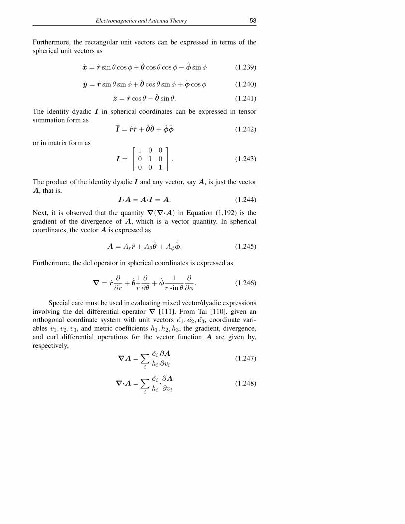
Electromagnetics and Antenna Theory 53
Furthermore, the rectangular unit vectors can be expressed in terms of thespherical unit vectors as
x = r sin θ cosφ+ θ cos θ cosφ− φ sinφ (1.239)
y = r sin θ sinφ+ θ cos θ sinφ+ φ cosφ (1.240)
z = r cos θ − θ sin θ. (1.241)
The identity dyadic I in spherical coordinates can be expressed in tensorsummation form as
I = rr + θθ + φφ (1.242)
or in matrix form as
I =
1 0 00 1 00 0 1
. (1.243)
The product of the identity dyadic I and any vector, say A, is just the vectorA, that is,
I·A = A·I = A. (1.244)
Next, it is observed that the quantity ∇(∇·A) in Equation (1.192) is thegradient of the divergence of A, which is a vector quantity. In sphericalcoordinates, the vectorA is expressed as
A = Arr +Aθθ +Aφφ. (1.245)
Furthermore, the del operator in spherical coordinates is expressed as
∇ = r∂
∂r+ θ
1
r
∂
∂θ+ φ
1
r sin θ
∂
∂φ. (1.246)
Special care must be used in evaluating mixed vector/dyadic expressionsinvolving the del differential operator ∇ [111]. From Tai [110], given anorthogonal coordinate system with unit vectors e1, e2, e3, coordinate vari-ables v1, v2, v3, and metric coefficients h1, h2, h3, the gradient, divergence,and curl differential operations for the vector function A are given by,respectively,
∇A =∑i
eihi
∂A
∂vi(1.247)
∇·A =∑i
eihi·∂A∂vi
(1.248)
54 Electromagnetics and Antenna Technology
∇×A =∑i
eihi×∂A∂vi
. (1.249)
In spherical coordinates, the coordinate variables are v1 = r, v2 = θ, v3 = φ,the unit vectors are e1 = r, e2 = θ, e3 = φ, and the metric coefficients areh1 = 1, h2 = r, h3 = r sin θ.
It is worthwhile utilizing the del operator ∇ as follows. A dyadic suchas∇A can be formed either as a summation by Equation (1.247) or by matrixoperation as
∇A =∇AT =
(r) ∂∂r(θ)1
r∂∂θ
(φ) 1r sin θ
∂∂φ
[ (r)Ar (θ)Aθ (φ)Aφ]. (1.250)
The nine terms of the tensor summation of Equation (1.250) are computedusing the chain rule for the unit vectors. For example, the rr dyad term isgiven by
(∇A)rr = r[r∂
∂rAr +Ar
∂r
∂r] (1.251)
and noting ∂r∂r = 0. The remaining eight terms of Equation (1.250) are
computed similarly, with the result expressed as the tensor summation
∇A = ∂Ar∂r rr + ∂Aθ
∂r rθ +∂Aφ∂r rφ
+(1r∂Ar∂θ −
Aθr )θr + (1
r∂Aθ∂θ + Ar
r )θθ + 1r∂Aφ∂θ θφ
+( 1r sin θ
∂Ar∂φ −
Aφr )φr + ( 1
r sin θ∂Aθ∂φ − cot θ
Aφr )φθ
+( 1r sin θ
∂Aφ∂φ + cot θAθr + Ar
r )φφ.
(1.252)
Earlier it was stated (see Equation [1.205]) that the electric field causedby the source current density J is given by
E(r) = −jωµ[I +1
k2∇∇]·
∫VJ(r′)
e−jk|r−r′|
4π|r − r′|dv′ (1.253)
and now it is desired to solve this equation under far-field conditions. Usingthe vector identity
(∇∇)·A =∇(∇·A), (1.254)
it follows that the gradient of the divergence of a vector functionA is [110, p.126]
∇(∇·A) =∑i
eihi
∂
∂vi
∑j
ejhj·∂A∂vj
, (1.255)
Electromagnetics and Antenna Theory 55
and then performing the partial derivative operation using the chain rule yields
∇(∇·A) =∑i
∑j
eihi
[∂
∂vi
(ejhj
)·∂A∂vj
+ejhj· ∂
2A
∂vi∂vj
]. (1.256)
Using the spherical coordinate parameters in Equation (1.256) yields for thei = 1, j = 1 term
∇(∇·A)i=1,j=1 = r
[∂
∂r(r)·∂A
∂r+ r·∂
2A
∂r2
], (1.257)
and since ∂r/∂r = 0, it follows that
∇(∇·A)i=1,j=1 = rr·∂2A
∂r2. (1.258)
Similarly, Equation (1.256) yields for the i = 1, j = 2 term
∇(∇·A)i=1,j=2 = r
[∂
∂r
(θ
r
)·∂A∂θ
+θ
r· ∂
2A
∂r∂θ
], (1.259)
and since ∂∂r (θ/r) = −θ/r2, it follows that
∇(∇·A)i=1,j=2 = rθ
[− 1
r2·∂A∂θ
+1
r· ∂
2A
∂r∂θ
]. (1.260)
Next, for the i = 1, j = 3 term,
∇(∇·A)i=1,j=3 = rφ
[− 1
r2 sin θ·∂A∂φ
+1
r sin θ· ∂
2A
∂r∂φ
]. (1.261)
In solving for the far-zone radiation pattern function of an antenna, typicallyonly a 1/r variation is retained with all other terms involving 1/r2, 1/r3
ignored. All of the remaining terms of ∇(∇·A)i,j for i = 2, 3 have higher-order dependence on inverse r and can be neglected. Thus, in the far field, thegradient of the divergence of the magnetic vector potential can be expressedas
∇(∇·A)FF = rr·∂2A
∂r2. (1.262)
The electric field given by Equation (1.192) can be written as
E = −jω[A+1
k2∇ (∇·A)] (1.263)
56 Electromagnetics and Antenna Technology
where k2 = ω2µε. Now, using Equation (1.262) in Equation (1.263) yields anexpression for the far-zone vector electric field
EFF = −jω[A+
1
k2rr·∂
2A
∂r2
]. (1.264)
Repeating Equation (1.197) for the magnetic vector potential
A(r) = µ
∫VJ(r′)
e−jk|r−r′|
4π|r − r′|dv′ (1.265)
and in computing the far field of a radiating source, Equation (1.265) can besimplified by approximating |r − r′| in the exponential argument as
|r − r′| ≈ r − r·r′ (1.266)
and usingkr >> 1 (1.267)
such that the factor |r − r′| in the denominator can be replaced by r. Thus,under far-field conditions, Equation (1.265) can be expressed as
AFF = µe−jkr
4πr
∫VJ(r′)ejkr·r′ dv′. (1.268)
Define a far-field vector current moment f(θ, φ) in spherical coordinatesas the integral in Equation (1.268) as
f(θ, φ) = frr + fθθ + fφφ =
∫VJ(r′)ejkr·r′ dv′. (1.269)
Using Equation (1.269) in Equation (1.268) yields the far-field magneticvector potential as
AFF = µe−jkr
4πrf(θ, φ). (1.270)
Now, comparing Equations (1.263) and (1.264), the contribution of∇(∇·A) to the far-field vector electric field depends on the second partialderivative of the free-space Green’s function. Performing the first partialderivative operation, it follows that
∂
∂r
[e−jkr
4πr
]= −jke
−jkr
4πr− e−jkr
4πr2, (1.271)
Electromagnetics and Antenna Theory 57
and then the second partial derivative is determined to be
∂2
∂r2
[e−jkr
4πr
]= −k2 e
−jkr
4πr+ 2jk
e−jkr
4πr2+ 2
e−jkr
4πr3(1.272)
and in the far field, the 1/r2 and 1/r3 terms go to zero compared to 1/r, andthus only the 1/r term contributes to the far-zone electric field. Thus, in thefar field,
∂2
∂r2
[e−jkr
4πr
]FF
= −k2 e−jkr
4πr(1.273)
and it follows that
∂2AFF
∂r2=
∂2
∂r2
[µe−jkr
4πrf(θ, φ)
]= −µk2 e
−jkr
4πrf(θ, φ). (1.274)
Note: another derivative of the scalar Green’s function, in this case divided byr, used subsequently in evaluating Equation (1.457), is given by
∂
∂r
[e−jkr
4πr2
]= −jke
−jkr
4πr2− 2e−jkr
4πr3. (1.275)
Substituting Equations (1.270) and (1.274) in Equation (1.264) yields
EFF = −jω[µe−jkr
4πrf(θ, φ)− µe
−jkr
4πrrr·f(θ, φ)
], (1.276)
which can also be expressed in dyadic/vector notation as
EFF = −jωµe−jkr
4πr(I − rr)·f(θ, φ) (1.277)
whereI − rr = θθ + φφ. (1.278)
Now using Equations (1.278) and (1.235) and performing the dyadic/vectoroperations in Equation (1.277) yields the vector form of the desired expressionfor the far-zone electric field as
EFF = −jωµe−jkr
4πr(θfθ + φfφ). (1.279)
Noting that1
r
∂
∂r(rEFF) = −jkEFF (1.280)

58 Electromagnetics and Antenna Technology
the far-zone magnetic field is then computed using the far-zone electric field(Equation [1.279]), the curl operation (1.94) and vector cross product (1.96)as
HFF =1
−jωµ∇×EFF(r) =
kr
ωµ×EFF(r). (1.281)
Performing the vector operation in Equation (1.281) yields
HFF = −jk e−jkr
4πr(φfθ − θfφ). (1.282)
Referring to Equation (1.399) and using Equations (1.279) and (1.281), thetime-average Poynting’s power density in the far zone is now computed as
< S >=1
2ReE×H∗ = r
1
2
õ
ε
(k
4πr
)2
(|fθ|2 + |fφ|2). (1.283)
Return now to the general form of the electric field given by Equa-tion (1.205) and express the electric field in terms of the scalar Green’sfunction g(r, r′) as
E(r) = −jωµ[I +1
k2∇∇]·
∫VJ(r′)g(r, r′) dv′. (1.284)
Now the bracketed terms in front of the integral depend only on the unprimedcoordinates and can be moved inside the integral in Equation (1.284) andrearranging yields
E(r) = −jωµ∫V
[[I +
1
k2∇∇]g(r, r′)
]·J(r′) dv′. (1.285)
It is assumed here that the observation point is outside the source volume.In cases where the observation point is within the source volume, additionalintegration terms must be taken into account [116]. The dyadic Green’sfunctionG(r, r′) can now be expressed in terms of the scalar Green’s functiong(r, r′) as
G(r, r′) = [I +1
k2∇∇]g(r, r′). (1.286)
Thus, Equation (1.285) can be rewritten in the more compact dyadic Green’sfunction representation as
E(r) = −jωµ∫VG(r, r′)·J(r′) dv′. (1.287)

Electromagnetics and Antenna Theory 59
The dyadic and scalar Green’s functions are now examined in moredetail. Let us return now to the time-harmonic form of Maxwell’s equationscorresponding to Equations (1.145) and (1.146), that is,
∇×E(r) = −jωµH(r)−M(r) (1.288)
∇×H(r) = jωεE(r) + J(r) (1.289)
where µ and ε are assumed to be complex in general and the current densitiesJ and M are source currents. Assuming that the equivalent magnetic currentis zero, that is, M = 0, H(r) can be eliminated from Equation (1.288) bytaking the curl of the curl of E as
∇×∇×E(r) = −jωµ∇×H(r) (1.290)
and substituting Equation (1.289) yields
∇×∇×E(r) = −jωµjωεE(r)− jωµJ(r) (1.291)
and rearranging yields the following inhomogeneous wave equation forE(r),that is,
∇×∇×E(r)− k2E(r) = −jωµJ(r). (1.292)
To solve Equation (1.292), the dyadic Green’s function method can be usedfor an arbitrary response vector function y and source vector function f asfollows.
Let Lop be a linear differential operator such that
Lopy(r) = f(r). (1.293)
It is desired to determine the dyadic Green’s function G that is given by thesolution to
LopG(r, r′) = Iδ(r − r′) (1.294)
and boundary conditions must be satisfied. A solution for y(r) is then
y(r) =
∫G(r, r′)·f(r′)dv′. (1.295)
Next, from Equation (1.287), in terms of the complex permeability µ, thevector electric field can be expressed in terms of the dyadic Green’s functionas
E(r) = −jωµ∫VG(r, r′)·J(r′) dv′ (1.296)
where it should be noted that, in addition, any boundary conditions must beenforced. In Equation (1.292), it is desirable to express the source density in

60 Electromagnetics and Antenna Technology
terms of the primed coordinate system. One way to achieve this transformationfrom unprimed to primed coordinates is to make use of the three-dimensionaldelta function δ(r − r′) as described by Kong [3, p. 496] as
J(r) =
∫Vδ(r − r′)I·J(r′)dv′. (1.297)
Substituting Equations (1.296) and (1.297) in Equation (1.292) yields
−jωµ∫V ∇×∇×G(r, r′)·J(r′) dv′ + jωµk2
∫V G(r, r′)·J(r′) dv′
= −jωµ∫V δ(r − r′)I·J(r′)dv′.
(1.298)Since the integral operation involving J(r′) appears in each term ofEquation (1.298), it follows that the integral operation on J(r′) and the jωµquantity can be eliminated, which gives
∇×∇×G(r, r′)− k2G(r, r′) = Iδ(r − r′). (1.299)
Substituting Equation (1.286) in Equation (1.299 yields
∇×∇×[I +
1
k2∇∇
]g(r, r′)− k2
[I +
1
k2∇∇
]g(r, r′) = Iδ(r − r′).
(1.300)Now Equation (1.300) can be simplified by first observing that the curl of agradient of an arbitrary vector is zero, that is,
∇×∇V = 0, (1.301)
and recognizing that the gradient of the scalar Green’s function g(r, r′) is avector, it follows that
1
k2∇×∇×∇∇g(r, r′) =
1
k2∇×[∇×∇(∇g(r, r′))] = 0. (1.302)
Thus, Equation (1.300) reduces to
∇×∇×Ig(r, r′)− k2[I +
1
k2∇∇
]g(r, r′) = Iδ(r − r′). (1.303)
Next, using the dyadic identity
∇×∇×D =∇(∇·D)−∇2D, (1.304)
it follows that∇×∇×Ig =∇(∇·Ig)−∇2(Ig); (1.305)

Electromagnetics and Antenna Theory 61
but from the identity∇·(φI) =∇φ (1.306)
it follows that∇·Ig =∇g. (1.307)
Therefore,∇×∇Ig =∇∇g − I∇2g. (1.308)
Substituting Equation (1.308) in Equation (1.303) yields
∇∇g(r, r′)− I∇2g(r, r′)− k2[I +
1
k2∇∇
]g(r, r′) = Iδ(r − r′),
(1.309)and canceling like terms yields the simplified inhomogeneous wave equation
∇2g(r, r′) + k2g(r, r′) = −δ(r − r′). (1.310)
To determine the functional form of the scalar Green’s function g(r, r′) inEquation (1.310), it is necessary first to solve the homogeneous form of theequation and then invoke the boundary conditions in the inhomogeneous case.To simplify the solution for g, shift the source position to the origin, whichmeans r′ = 0. Thus, Equation (1.310) can now be expressed as
∇2g(r) + k2g(r) = −δ(r), (1.311)
and it is observed that the solution for g(r) is independent of the sphericalcoordinate angles θ and φ.
In spherical coordinates, the Laplacian of a scalar g that depends onlyon r can be expressed as [3, p. 18]
∇2g(r) =1
r2
∂
∂r
[r2∂g(r)
∂r
]=
1
r
∂2
∂r2(rg(r)). (1.312)
Thus, Equation (1.311) can be rewritten as the inhomogeneous form
1
r
d2
dr2(rg(r)) + k2g(r) = −δ(r). (1.313)
If the observation point is not at the origin, that is, r 6= 0, then Equa-tion (1.313) reduces to the homogeneous differential equation
d2
dr2(rg(r)) + k2rg(r) = 0. (1.314)

62 Electromagnetics and Antenna Technology
The solution to the differential equation expressed by Equation (1.314) is anoutgoing wave of the form
g(r) = Ce−jkr
r. (1.315)
To determine the constant C in Equation (1.315), it is necessary to satisfythe boundary conditions at infinity and at the origin where the point source islocated. In the limit as r →∞ in Equation (1.315) g(r)→ 0, which satifiesthe condition that the wave amplitude must attenuate to zero because of fieldspreading loss. To satisfy the boundary condition at the origin, it is necessaryto integrate Equation (1.311) over an infinitesimal sphere of radius rs centeredat the origin and let the sphere radius tend to zero. Expressing the Laplacianoperation on the scalar g as
∇2g =∇·∇g (1.316)
and noting that the delta function acts as a sampling function, that is,∫f(x)δ(x− xo) dx = f(xo) (1.317)
and substituting Equation (1.315) in Equation (1.311), the following integralequation can be written as
C
∫V∇·(∇e−jkr
r
)dv + C
∫Vk2 e
−jkr
rdv = −
∫Vδ(r) dv = −1. (1.318)
Now, applying the divergence theorem∫V∇·A dv =
∮SA·n ds (1.319)
to the first term in Equation (1.318) yields
C
∫V∇·(∇e−jkr
r
)dv = C
∮Sn·r ∂
∂r
(e−jkr
r
)ds. (1.320)
The surface integral in Equation (1.320) is evaluated as follows. Noting thatfor the assumed spherical volume n = r and ds = r2 sin θ dθ dφ, the surfaceintegral in the first term of Equation (1.318) becomes∮
Sddr
(e−jkr
r
)ds =
∫ 2π0
∫ π0
[ddr
(e−jkr
r
)]r2 sin θ dθ dφ
=∫ 2π
0
∫ π0
[e−jkr(−jkr−1)
r2
]r=rs
sin θ dθ dφ
=∫ 2π
0
∫ π0
[e−jkr(−jkr − 1)
]r=rs→0
sin θ dθ dφ
=∫ 2π
0
∫ π0 [−1] sin θ dθ dφ = −4π.
(1.321)

Electromagnetics and Antenna Theory 63
Now the integral in the second term in Equation (1.320) is evaluated as∫V k
2 e−jkr
r dv = k2∫ rs0
∫ 2π0
∫ π0e−jkr
r r2 sin θ dr dθ dφ
= 4πk2∫ rs→00 re−jkrdr
= 4πk2[e−jkr
k2(−jkr − 1)
]rs→0
0= 0.
(1.322)
Substituting the results of Equations (1.321) and (1.322) in Equation (1.318),it follows that
C =1
4π, (1.323)
and substituting the result for the constant in Equation (1.315) yields the scalarGreen’s function as a function of r
g(r) =e−jkr
4πr. (1.324)
Since the radius r in Equation (1.324) is the distance between the source andthe observation point, it is possible to shift the source to the vector position r′,and thus the transformed distance between the source and observation pointbecomes |r − r′|. Therefore, the general form of the scalar Green’s functionis given by
g(r, r′) =e−jk|r−r
′|
4π|r − r′|. (1.325)
Substituting Equation (1.325) in Equation (1.286) yields the dyadic Green’sfunction in terms of the scalar Green’s function as
G(r, r′) = [I +1
k2∇∇]
e−jk|r−r′|
4π|r − r′|. (1.326)
The electric field is then determined by using Equation (1.326) in Equa-tion (1.296).
1.5 Boundary Conditions
In determining the solution of electromagnetic fields for a general antennaor scattering problem, it is necessary to satisfy boundary conditions betweendifferent media for the tangential and normal field components. The boundaryconditions depend on the type of media and also whether any chargesor currents are present at the interface between the media. To derive theboundary conditions from Maxwell’s equations, two vector identities areneeded, namely the divergence theorem expressed as∫
V∇·A dv =
∮SA· ds (1.327)
64 Electromagnetics and Antenna Technology
and Stokes’ theorem expressed as∫S
(∇×A)·ds =
∮CA·dl. (1.328)
To be completely general and allow for boundary conditions for antennaapertures, it is necessary to include the contribution from the fictitious mag-netic current density M in Maxwell’s curl of E equation as a mathematicalconvenience, that is,
∇×E = −M − ∂B
∂t. (1.329)
Note, the magnetic current density has units of V/m2.The divergence theorem given by Equation (1.327) states that the volume
integral of the divergence of A is equal to the outward flux of the vector fieldA through the surface S enclosing the volume V . Assuming that A and thecurl of A are continuous, Stokes’ theorem given by Equation (1.328) statesthat the curl of A over the open surface S bounded by C is equal to thecirculation ofA around the closed path C.
Consider now Figure 1.7, which shows two media separated by aninterface surface that can be of arbitrary shape and can support surface chargesρs and surface currents Js andM s. To determine the boundary conditions forthe normal field components, consider Figure 1.8. From Maxwell’s divergenceofD equation and the divergence theorem, we can write∫
V∇·Ddv =
∮SA·ds =
∫Vρdv (1.330)
where ρ is the volume charge density. In the limit where ∆h approaches zero,only the top and bottom of the cylindrical box contribute, such that in vectornotation,
n·(D2 −D1) = ρs (1.331)
where ρs is the surface charge density. Similarly, it can be shown that
n·(B2 −B1) = 0. (1.332)
Now, referring to Figure 1.9 from Maxwell’s curl ofE equation including thefictitious magnetic current density and Stokes’ theorem, we can write∫
S(∇×E)·ds =
∮CE·dl = −
∫SM ·ds−
∫S
∂B
∂t·ds. (1.333)
As ∆h goes to zero, the term involving the integral of B goes to zero, andnow in vector form, Equation (1.333) becomes
(E2 −E1)×n = M s (1.334)
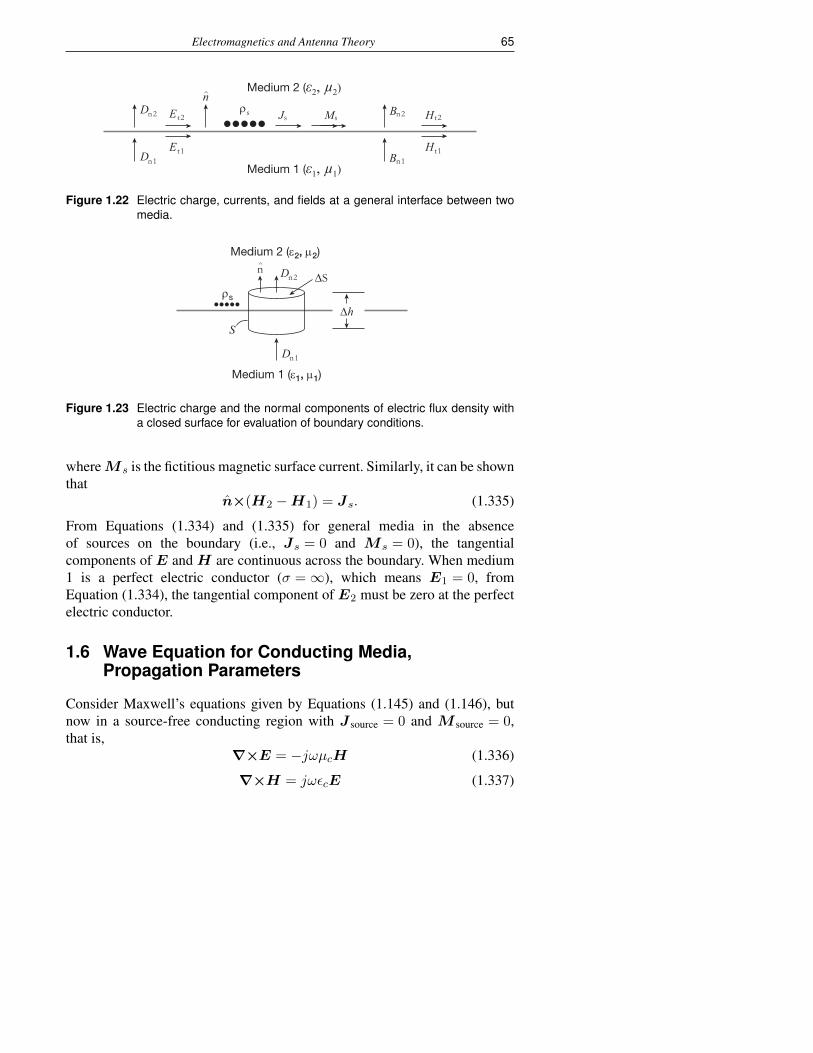
Electromagnetics and Antenna Theory 65
t2Dn2
^
n1
Medium 2 (ε2, µ2)
Medium 1 (ε1, µ1)
n2
n1
t2
t1t1
s sρs
D
E J M
E H
H
B
Bn
Figure 1.22 Electric charge, currents, and fields at a general interface between twomedia.
Dn2n
Dn1
Medium 2 (ε2, µ2)
Medium 1 (ε1, µ1)
ρs
∆S
∆hS
Figure 1.23 Electric charge and the normal components of electric flux density witha closed surface for evaluation of boundary conditions.
whereM s is the fictitious magnetic surface current. Similarly, it can be shownthat
n×(H2 −H1) = Js. (1.335)
From Equations (1.334) and (1.335) for general media in the absenceof sources on the boundary (i.e., Js = 0 and M s = 0), the tangentialcomponents of E and H are continuous across the boundary. When medium1 is a perfect electric conductor (σ =∞), which means E1 = 0, fromEquation (1.334), the tangential component of E2 must be zero at the perfectelectric conductor.
1.6 Wave Equation for Conducting Media,Propagation Parameters
Consider Maxwell’s equations given by Equations (1.145) and (1.146), butnow in a source-free conducting region with J source = 0 and M source = 0,that is,
∇×E = −jωµcH (1.336)
∇×H = jωεcE (1.337)

66 Electromagnetics and Antenna Technology
Et2Ms
n^Medium 2 (ε2, µ2)
Medium 1 (ε1, µ1)
S
∆w∆hEt1
Figure 1.24 Magnetic current and tangential E fields with a closed contour forevaluation of boundary conditions.
∇·D = 0 (1.338)
∇·B = 0. (1.339)
Taking the curl of Equation (1.336) and substituting Equations (1.149) and(1.337) yields
∇×∇×E = −jωµcjωεcE = −jωµc(σ + jωε′)E (1.340)
or∇×∇×E = −jωµcjωεcE = ω2µcεcE (1.341)
and defining the complex wavenumber k here as
k = ω√µcεc (1.342)
it follows that∇×∇×E = k2E. (1.343)
By using the vector identity
∇×∇×E =∇(∇·E)−∇2E (1.344)
and noting that the divergence of E is zero by Equation (1.338), it followsthat
∇2E + k2E = 0, (1.345)
which is a form of the vector wave equation in complex media. A similar waveequation involving the vector magnetic field is given by
∇2H + k2H = 0. (1.346)
The vector wave equations expressed by Equations (1.345) and (1.346)are also commonly expressed as
∇2E − γ2E = 0 (1.347)

Electromagnetics and Antenna Theory 67
∇2H − γ2H = 0 (1.348)
where γ is the complex propagation constant. The above vector waveequations allow for spherical, cylindrical, and plane wave solutions.
For example, consider a z-polarized plane wave propagating in the xdirection as given by the linearly polarized electric field
E(x) = e−γxz. (1.349)
The plane-wave function given by Equation (1.349) is a solution of Equa-tion (1.347), which can be verified by observing that the wave equation canbe expressed in cartesian coordinates as
∇2E − γ2E =∂2E
∂x2− γ2E = 0 (1.350)
and then performing the partial derivative operation.The relationship between the complex propagation constant γ and the
complex wavenumber k is
γ = jk = jω√µcεc. (1.351)
Thus,γ2 = −k2 = −ω2µcεc. (1.352)
By using Equation (1.340), it follows that
γ2 = jωµc(σ + jωε′). (1.353)
Assume now an electrically conducting medium, and then it is readily shownthat the propagation constant can be expressed as
γ = ±√jωµ′(σ + jωε′) = ±jω
√µ′ε′
√1− j σ
ωε′. (1.354)
Again, the quantity (refer to Equation [1.355])
σ
ωε′=ε′′
ε′= tan δ (1.355)
is referred to as the electric loss tangent or dissipation factor. Both σ andtan δ are used in tables of dielectric characteristics of materials. It is commonto express the complex propagation constant as
γ = α+ jβ (1.356)
68 Electromagnetics and Antenna Technology
where α is the attenuation constant in nepers/meter and β is the phase constantin radians/meter. Again, the complex wavenumber is expressed as
jk = α+ jβ (1.357)
and either way of analyzing the wave propagation provides the same results.The units of nepers/meter can be converted to decibels by multiplying by thefactor 8.686. The units of radians/meter can be converted to degrees/meter bymultiplying by the factor 180/π = 57.296.
The constants α and β are found by setting Equation (1.354) equalto Equation (1.356) and then squaring both sides, equating the real andimaginary parts, and solving the pair of simultaneous equations, with theresult
α =ω√µ′ε′√2
√
1 +
(σ
ωε′
)2
− 1
1/2
(1.358)
β =ω√µ′ε′√2
√
1 +
(σ
ωε′
)2
+ 1
1/2
. (1.359)
The wavelength λ in the lossy dielectric is then computed from the phaseconstant given by Equation (1.359) as
λ =2π
β. (1.360)
The intrinsic wave impedance η is related to the ratio of the electric andmagnetic fields and in lossy dielectric material is given by [8]
η =
õ
ε=
√jωµ′
σ + jωε′=
√µ′
ε′1√
1− j σωε′
. (1.361)
In free space, the electrical conductivity σ is equal to zero, and it follows fromEquation (1.361) that the free-space intrinsic wave impedance is
ηfree space =
√µoεo
= 120π = 376.99 ≈ 377 ohms. (1.362)
In the general media case, in which both electric and magnetic loss arepresent, the constants α and β are determined from Equations (1.352) and(1.356) using Equations (1.142) and (1.143), by solving the simultaneousequations for the real and imaginary components with the result
α =ω√µ′ε′√2
√(1 + tan2 δe) (1 + tan2 δm)− (1− tan δe tan δm)
1/2
(1.363)
Electromagnetics and Antenna Theory 69
β =ω√µ′ε′√2
√(1 + tan2 δe) (1 + tan2 δm) + (1− tan δe tan δm)
1/2
(1.364)where
tan δe =ε′′
ε′=
σeωε′
=σe
ωεoε′r(1.365)
and
tan δm =µ′′
µ′=σmωµ′
=σm
ωµoµ′r(1.366)
are the electric and magnetic loss tangents, respectively. For general lossymedia, the wave impedance is given by
η =
õ
ε=
√µ′ − jµ′′ε′ − jε′′
=
√µ′
ε′
√1− j tan δm1− j tan δe
. (1.367)
Taking account of boundary conditions as described in Section 1.7, for normalangle of incidence of a plane wave, the reflection coefficient Γ for a uniformplane wave traveling in medium 1 and reflecting at the boundary of medium 2is given by
Γ =η2 − η1
η2 + η1, (1.368)
and the transmission coefficient T for a plane wave at normal incidencetransmitted into medium 2 is given by
T =2η2
η2 + η1(1.369)
where η1 is the impedance of medium 1 and η2 is the impedance of medium 2.The more general cases of plane-wave incidence, including oblique incidence,polarization effects, and different media, are covered by Balanis [2, pp. 173–257].
It is convenient to have a simple equation for computing the wavepropagation between any two points in the near field of an isolatedtransmitting antenna in conducting media. Consider a time-harmonic sourceradiating a spherical wave into an infinite homogeneous conducting medium.For an isotropic radiator and suppressing the ejωt time dependence whereω = 2πf , the electric field as a function of range r can be expressed in phasornotation as a spherical wave
E(r) = Eoe−γr
r(1.370)
70 Electromagnetics and Antenna Technology
where Eo is a constant and γ is the propagation constant given byEquation (1.354). For some cases in which the 1/r dependence can beignored, a plane wavefront approximation to Equation (1.370) can be used.For example, a plane wavefront propagating along the x-axis can be expressedas
E(x) = Eoe−γx. (1.371)
Equation (1.370) or Equation (1.371) can be used in a simplified ray-tracinganalysis to compute the approximate electric field, generated by one or moretransmitting antennas, at any point in a homogeneous lossy dielectric. Ifwe let the electric field at the rectangular coordinates (x, y, z) due to thenth transmitting antenna in an array of N transmitting antennas be denotedas En(x, y, z), then the total electric field of the transmitting array can beexpressed as the following summation,
Etotal(x, y, z) =N∑n=1
En(x, y, z). (1.372)
For a transmitting point source at the origin, the amplitude of the electricfield at range r1 is given by
|E(r1)| = Eoe−αr1
r1(1.373)
and at range r2 by
|E(r2)| = Eoe−αr2
r2. (1.374)
The total propagation loss between ranges r1 and r2 is found by taking theratio of Equations (1.374) and (1.373) as
|E(r2)||E(r1)|
=r1
r2e−α(r2−r1). (1.375)
The field attenuation Aα in decibels from range r1 to range r2 caused by thelossy dielectric is simply
Aα = 20 log10(e−α(r2−r1)). (1.376)
If we let d = r2 − r1, the above equation can be written in a convenient formas
Aα = 20 log10(e−αd), (1.377)
which is the relative field attenuation as a function of distance d into a lossydielectric or transmission loss of a plane wave in decibels per meter. The

Electromagnetics and Antenna Theory 71
attenuation constant α has units of nepers per unit length or typically in theliterature of nepers per meter (Np/m), where neper is dimensionless. If d is onemeter and α = 1 Np/m, then the field strength in decibels is 20 log10(e−1) =20 log10 |0.368| = −8.686 dB. Thus, the attenuation in decibels per meter is8.686 times the attenuation constant in nepers per meter. If the attenuationconstant is expressed in nepers/cm, then to convert to attenuation in decibelsper cm, the multiplying factor remains 8.686. Similarly, the 1/r attenuationloss Ar in decibels is
Ar = 20 log10
r1
r2. (1.378)
1.7 Electromagnetic Energy Flow
To demonstrate that an electromagnetic field can transfer electromag-netic energy into an electrically conducting volume (e.g., soil as in aground-penetrating radar application), consider the following application ofMaxwell’s curl equations in the time domain in a source-free region whereJ source = 0 and M source = 0. Starting with the curl of the instantaneousmagnetic field as in Equation (1.86), substitute Equations (1.104) and (1.122)with the result
∇×H(r, t) = σE + ε′∂E
∂t. (1.379)
Next, the curl of the instantaneous electric field from Equation (1.85) is givenby
∇×E(r, t) = −µ′∂H∂t
. (1.380)
Fundamentally, it is desired to derive a power-flow expression for the electricand magnetic fields. The electric field has units of volts/meter and themagnetic field has units of amperes/meter. The product of volts/meter andamperes/meter produces watts/meter2, which is power density. There are twopossibilities for manipulating the electric and magnetic field expressions toproduce a relation for power density, either a dot product or a cross productof the two field quantities. To produce a meaningful relation here, the crossproduct is the desired vector operation on the electric and magnetic fieldvectors. A vector identity will also be needed to convert to the desired fieldrelation. Of the available general vector identities, the one that applies here is
∇·(A×B) = B·(∇×A)−A·(∇×B). (1.381)
On the basis of the vector identity in Equation (1.381), it is observed that thedesired mathematical manipulations are to dot the electric field into the curlof the magnetic field and to dot the magnetic field into the curl of the electric

72 Electromagnetics and Antenna Technology
field. Once these manipulations are done, the desired cross product betweenE andH will appear. Thus, from Equations (1.379), (1.380), and (1.381) andby using J ·E = E·J , it follows that
E·(∇×H) = J ·E +E·ε′∂E∂t
= J ·E +1
2ε′∂E2
∂t(1.382)
and
H·(∇×E) = −H·µ′∂H∂t
= −1
2µ′∂H2
∂t. (1.383)
Simplifying and subtracting Equation (1.382) from Equation (1.383) yields
E·(∇×H)−H·(∇×E) = J ·E +1
2ε′∂E2
∂t+
1
2µ′∂H2
∂t(1.384)
or applying the vector identity Equation (1.381) in Equation (1.384) yields
∇·(E×H) = −J ·E − 1
2ε′∂E2
∂t− 1
2µ′∂H2
∂t(1.385)
and now integrating over a volume of media∫V∇·(E×H)dv = −
∫VJ ·Edv − ∂
∂t
∫V
[1
2ε′E2 +
1
2µ′H2]dv. (1.386)
The divergence theorem for any vector A for a closed surface S enclosingvolume V is given by ∫
V∇·Adv =
∮SA·nds (1.387)
where dv is the elemental volume and ds is the elemental area perpendicularto the outward unit normal n. Thus, applying Equation (1.387) to the left-handside of Equation (1.386) yields∫
V∇·(E×H)dv =
∮S
(E×H)·nds. (1.388)
Finally, Equation (1.386) reduces to∮S
(E×H)·nds = −∫VJ ·Edv − ∂
∂t
∫V
[1
2ε′E2 +
1
2µ′H2]dv. (1.389)
The term on the left side of Equation (1.389) represents the net inward flux ofthe vector
P (r, t) = E(r, t)×H(r, t). (1.390)
Electromagnetics and Antenna Theory 73
In Equations (1.389) and (1.390), the vector quantityP (r, t) = E(r, t)×H(r, t)is known as the instantaneous Poynting vector (due to J.H. Poynting[104]) and can be interpreted as the instantaneous power-flow density inwatts/meter2 at each observation point (r) on the surface S, or equivalentlythe power delivered to the volume V by external electromagnetic sources.Equation (1.389) is referred to as the integral form of Poynting’s theoremand describes conservation of energy for electromagnetic waves. FromEquation (1.104), it follows that
J ·E = σE·E = σ|E|2 (1.391)
where the dot product of the real vector E with itself is just the magnitudeof E squared. The first integral term on the right side of Equation (1.389)involving J ·E = σ|E|2 represents the instantaneous ohmic losses within thevolume enclosed by the surface S. The integral in the second term on theright side of Equation (1.389) is the total energy (with units of watt-seconds =joules), due to electric and magnetic fields, stored within the volume V .
To understand the electromagnetic field energy transfer to conductivemedia such as lossy dielectrics, it is necessary to determine the time-averagepower delivered to and dissipated within the volume. The time-averagePoynting vector or time-average power density given by Equation (1.389) iscomputed over one period T as
P ave(r) =1
T
∫ T
0E(r, t)×H(r, t) dt (1.392)
where the period is equal toT = 2π/ω. (1.393)
Substituting the exponential forms given by Equations (1.114) and (1.115)into Equation (1.392) yields
P ave(r) =1
T
∫ T
0
[Re[E(r)ejωt]×Re[H(r)ejωt]
]dt. (1.394)
Making use of the relation
Re[AB] =1
2[AB +A∗B∗], (1.395)
it follows that
Re[E(r)ejωt]×Re[H(r)ejωt] =1
2[Eejωt +E∗e−jωt]×1
2[Hejωt +H∗e−jωt].
(1.396)
74 Electromagnetics and Antenna Technology
Expanding Equation (1.396) and using the relation (with * denoting conju-gate)
Re[E×H∗] =1
2[E×H∗ +E∗×H] (1.397)
it can be shown that Equation (1.394) reduces to
P ave =1
T
∫ 2πω
0
[1
2Re[E×H∗] +
1
4E×Hej2ωt +
1
4E∗×H∗e−j2ωt
]dt.
(1.398)It can be shown, by integration, that Equation (1.398) reduces to
P ave(r) =1
2Re[E×H∗], (1.399)
which is the desired expression for the time-average power density of theelectromagnetic field, or the time-average Poynting’s vector, which has unitsof watts/meter2.
As an example, for the case of a plane wave propagating in a conductingmedium, the electric field is given by
E(r) = η n×H(r) (1.400)
and the magnetic field is given by
H(r) = n×E(r)/η (1.401)
and thus, by substituting Equation (1.401) in Equation (1.399), it follows froma vector identity that the time-average Poynting vector for a plane wave isequal to
P ave(r) = n1
2|E(r)|2/η (1.402)
where n is the direction of propagation.Next, it is desired to quantify the average power deposition in a lossy
dielectric because this quantity is needed to determine the absorption ofelectromagnetic energy in any dielectric materials that the antenna mightbe constructed from, or in the case in which the antenna is radiating inthe presence of such lossy materials. Referring to Equation (1.389), for thefirst term on the right-hand side, the time-average power dissipation per unitvolume is computed over one period T as
Pd(r) =1
T
∫ T
0J(r, t)·E(r, t)dt. (1.403)
Electromagnetics and Antenna Theory 75
Substituting Equations (1.114) and (1.116) into Equation (1.403) yields
Pd(r) =1
T
∫ T
0
[Re[J(r)ejωt]·Re[E(r)ejωt]
]dt. (1.404)
Making use of the relation given in Equation (1.395), it follows that
Re[J(r)ejωt]·Re[E(r)ejωt] =1
2[Jejωt + J∗e−jωt]·1
2[Eejωt +E∗e−jωt].
(1.405)Using Equation (1.405) in Equation (1.404) and observing that the currentdensity J and electric field E are in phasor form, it follows that
J ·E∗ = σE·E∗ = σ|E|2 (1.406)
J∗·E = σE∗·E = σ|E|2 (1.407)
and it can be shown that
Pd =1
T
∫ T= 2πω
0
[1
2σ|E|2 +
1
4J ·Eej2ωt +
1
4J∗·E∗e−j2ωt
]dt. (1.408)
It also can be shown that Equation (1.408) reduces to
Pd(r) = Pave dissipated =1
2σ|E(r)|2, (1.409)
which is the desired expression for the time-average power dissipation per unitvolume of the lossy dielectric, which has units of watts/m3.
The specific absorption rate (SAR) [114] in the dielectric is the powerdissipated or absorbed per unit mass (W/kg) of the medium (lossy dielectric),so from Equation (1.409), it follows that
SAR(r) =Pd(r)
ρ=
σ
2ρ|E(r)|2 (1.410)
where ρ is the density of the medium in kg/m3. To estimate the initial lineartemperature rise ∆T versus time interval ∆t in a lossy dielectric that ischaracterized by the specific heat cd with units of kJ/(kg-C), the followingcalculation can be made:
∆T =SAR ∆t
cd(1.411)
where in Equation (1.411), it has been assumed that any thermal conductionor thermal boundary conditions have been ignored.

76 Electromagnetics and Antenna Technology
1.8 Fields of Short Electric and Magnetic Dipoles
1.8.1 Introduction
Arbitrarily shaped antennas can be considered to be composed of thesuperposition of a number of short electric dipoles and/or magnetic dipoles(electric loops) as depicted in Figure 1.10.
The closed-form expressions for the near-zone electromagnetic fields infree space resulting from an electrically short (Hertzian) dipole of length lwith current Ie along the z axis are given by [10]
Edipoler (r, θ) =
Ielej(ωt−βr)
2πεocos θ
(1
cr2+
1
jωr3
)(1.412)
Edipoleθ (r, θ) =
Ielej(ωt−βr)
4πεosin θ
(jω
c2r+
1
cr2+
1
jωr3
)(1.413)
Hdipoleφ (r, θ) =
Ielej(ωt−βr)
4πsin θ
(jω
cr+
1
r2
). (1.414)
Similarly, the near-zone electromagnetic fields for an electrically smallloop or short (small) magnetic dipole of length l with current Im along the zaxis are given by
H loopr (r, θ) =
Imlej(ωt−βr)
2πµocos θ
(1
cr2+
1
jωr3
)(1.415)
Hloopθ (r, θ) =
Imlej(ωt−βr)
4πµosin θ
(jω
c2r+
1
cr2+
1
jωr3
)(1.416)
Eloopφ (r, θ) =
Imlej(ωt−βr)
4πsin θ
(jω
cr+
1
r2
). (1.417)
Magnetic dipole or loopElectric dipole
θ
IeIm
rθ
a
r
Figure 1.25 Geometry for short electrical dipole with length l and current Ie and shortmagnetic dipole with length l and current Im (small electric current loopwith radius a).
Electromagnetics and Antenna Theory 77
In the far field, the terms involving 1/r2 and 1/r3 can be neglectedrelative to the 1/r term. Thus, the only significant far-field radiatingcomponents of the short vertical electric dipole are Eθ and Hφ. For the smallhorizontal loop antenna (short vertical magnetic dipole), the only significantfar-field radiating components are Eφ and Hθ. In each case, in the far field, itcan be shown that the ratio of the electric to magnetic field amplitude is equalto the impedance of free space. That is,
E
H= ηo. (1.418)
To derive the near-zone fields stated above, there are two approaches.One approach is to compute the magnetic vector potential A from the sourcecurrent J , and then the magnetic field H can be computed. The electricfield E is then obtained from the magnetic field H by using Maxwell’s curlequation. The other approach is to compute the electric field directly from thesource current J . Both approaches are discussed below.
In the first approach, the magnetic vector potential is needed and is givenby Equation (1.197), which is repeated below for general isotropic media:
A(r) = µ
∫VJ(r′)
e−jk|r−r′|
4π|r − r′|dv′. (1.419)
Repeating Equation (1.174), the magnetic fieldH in terms ofA is given by
H =1
µ∇×A. (1.420)
1.8.2 Derivation of Fields for z Hertzian Dipole
In the case of a z Hertzian dipole, let the electric current density be given by
J(r′) = zIelδ(r′) (1.421)
where the delta function δ(r′) is equal to unity when r′ = 0 and is equal tozero elsewhere. Substituting Equation (1.421) in Equation (1.419) yields
A(r) = zµIel
4π
e−jkr
r. (1.422)
To reduce the above equation, use the standard conversion from rectangularcomponents to spherical components, Ar
AθAφ
=
sin θ cosφ sin θ sinφ cos θcos θ cosφ cos θ sinφ − sin θ− sinφ cosφ 0
AxAyAz
. (1.423)
78 Electromagnetics and Antenna Technology
If the x and y components ofA are zero, the transformation reduces to
Ar = Az cos θ (1.424)
Aθ = −Az sin θ (1.425)
and note that the Aφ component is zero. Thus, from Equations (1.422),(1.424), and (1.425), it follows that
Ar = µIele−jkr
4πrcos θ (1.426)
Aθ = −µIele−jkr
4πrsin θ (1.427)
Aφ = 0. (1.428)
Since the Aφ component is zero and the φ variation of Ar and Aθ is zerofor a z-directed current, referring to Equation (1.93), the magnetic field H inspherical coordinates is reduced to
H =1
µ∇×A = φ
1
µr
[∂
∂r(rAθ)−
∂Ar∂θ
]. (1.429)
Performing the partial derivatives in Equation (1.429) yields the only nonzeromagnetic-field component
Hφ = jkIel sin θ
[1 +
1
jkr
]e−jkr
4πr. (1.430)
In general, the Maxwell curl equation for the magnetic field in time-harmonic form is Equation (1.146), which is repeated here as
∇×H = J source + jωεcE, (1.431)
and when the magnetic field is computed at a point removed from the source,the magnetic field expression is reduced to
∇×H = jωεE (1.432)
where it is now assumed that the complex permittivity is denoted by ε.Furthermore, using Equations (1.192) and (1.432), the electric field as afunction of the vector distance r from the source can be computed from eitherthe magnetic vector potentialA or magnetic fieldH as expressed below:
E(r) = −jωA− j
ωµε∇(∇·A) =
1
jωε∇×H. (1.433)

Electromagnetics and Antenna Theory 79
Substituting either Equations (1.426) and (1.427) or Equation (1.430) into(1.433) yields
Er(r, θ) = 2ηIel cos θ
[1
r+
1
jkr2
]e−jkr
4πr(1.434)
Eθ(r, θ) = jηkIel sin θ
[1 +
1
jkr− 1
(kr)2
]e−jkr
4πr(1.435)
Eφ = 0. (1.436)
The same near fields are computed for the z Hertzian dipole using thedyadic Green’s function approach described below. With this approach, theelectric field is computed directly, from which computation the magneticfield can be computed using Maxwell’s ∇×E equation. Repeating Equa-tion (1.205),
E(r) = −jωµ[I +1
k2∇∇]·
∫VJ(r′)
e−jk|r−r′|
4π|r − r′|dv′ (1.437)
and substituting Equation (1.421) in Equation (1.437) yields
E(r) = −jωµ[I +1
k2∇∇]·zIel
e−jkr
4πr(1.438)
or using spherical components (refer to Equation [1.241]) for z as
E(r) = −jωµ[I +1
k2∇∇]·
[[rIel cos θ − θIel sin θ
] e−jkr4πr
](1.439)
and then define
V =[rIel cos θ − θIel sin θ
] e−jkr4πr
= rVr + θVθ. (1.440)
Next, use the following identity
(∇∇)·V =∇(∇·V ) (1.441)
and it follows that Equation (1.439) becomes
E(r) = −jωµ[rVr + θVθ]− jωµ1
k2∇[∇·[rVr + θVθ
]]. (1.442)
Carrying out the vector operations in Equation (1.442) using Equation (1.256)yields the E-field components given previously in Equations (1.434), (1.435),and (1.436), which the reader can verify.

80 Electromagnetics and Antenna Technology
1.8.3 Derivation of Fields for an Arbitrarily Polarized HertzianDipole
The electric field produced by a source current density J with arbitrarypolarization unit vector p in infinite homogeneous space can be determinedas follows [3, p. 506]. Assume a Hertzian dipole with vector electric currentIel located at the origin, that is,
J(r′) = Ielδ(r′) (1.443)
whereIel = pIel (1.444)
and Ie is the magnitude of the current. Repeating Equation (1.205)
E(r) = −jωµ[I +1
k2∇∇]·
∫VJ(r′)
e−jk|r−r′|
4π|r − r′|dv′ (1.445)
and substituting in Equation (1.443) yields
E(r) = −jωµ[I +1
k2∇∇]·Iel
e−jkr
4πr. (1.446)
Using the vector identity given by Equation (1.441) and
∇·ψA = ψ(∇·A) +A·(∇ψ) (1.447)
and from Equation (1.95), it is observed that
∇·Iel = 0, (1.448)
and it follows that
∇∇·Iele−jkr
4πr=∇
[e−jkr
4πr(∇·Iel) + Iel·
(∇e−jkr
4πr
)]=∇
[Iel·
(∇e−jkr
4πr
)].
(1.449)Next, use the vector identity
∇(A·B) = (A·∇)B + (B·∇)A+A×(∇×B) +B×(∇×A).(1.450)
LettingA = Iel andB =∇(e−jkr/4πr) and using the vector identity
∇×(∇ψ) = 0 (1.451)
Electromagnetics and Antenna Theory 81
and noting that∇Iel = 0 and∇×Iel = 0, it follows that the rightmost sideof Equation (1.449) reduces to
∇[Iel·
(∇e−jkr
4πr
)]= (Iel·∇)∇e
−jkr
4πr. (1.452)
Now the gradient operation in Equation (1.452) is evaluated to be
∇(e−jkr
4πr
)= r
∂
∂r
(e−jkr
4πr
)= r
(−jk − 1
r
)e−jkr
4πr. (1.453)
Next, using Equation (1.453) in the right-hand side of Equation (1.452) yields
(Iel·∇)∇e−jkr
4πr= Iel·∇∇
e−jkr
4πr= Iel·
(∇r
(−jk − 1
r
)e−jkr
4πr
).
(1.454)To perform the gradient operation on the right-hand side of Equation (1.454),it is observed that
∇(rψ(r)) = r∇ψ(r) + ψ(r)∇r. (1.455)
Now let
ψ(r) =
(−jk − 1
r
)e−jkr
4πr(1.456)
and compute the gradient of ψ(r) as
∇ψ(r) =∇[(−jk − 1
r
)e−jkr
4πr
]= r
[−k2 +
2jk
r+
2
r2
]e−jkr
4πr.
(1.457)Using Equation (1.252) and the unit vector derivatives given below Equa-tion (1.235), it follows that
∇r =1
rθθ +
1
rφφ. (1.458)
Using the results of Equations (1.455), (1.456), (1.457), and (1.458), it followsthat the dyadic operation in Equation (1.454) is evaluated as
∇∇e−jkr
4πr= rr
[−k2 +
2jk
r+
2
r2
]e−jkr
4πr+[θθ + φφ
] [−jkr− 1
r2
]e−jkr
4πr.
(1.459)

82 Electromagnetics and Antenna Technology
Note: substituting Equation (1.459) in Equation (1.326) yields the explicitdyadic Green’s function for a point source at the origin as
G(r) = rr
[2j
kr+
2
k2r2
]e−jkr
4πr+[θθ + φφ
] [1− j
kr− 1
k2r2
]e−jkr
4πr.
(1.460)Using Equations (1.459), (1.449), and (1.242) in Equation (1.446) yields thenear-zone electric field for an arbitrary polarized Hertzian dipole at the originas
E(r) = −jωµe−jkr
4πr
[[1− j
kr− 1
k2r2
]Iel + r (r·Iel)
[−1 +
3j
kr+
3
k2r2
]].
(1.461)The near-zone magnetic field is then determined from Maxwell’s curl of Eequation as
H(r) = − 1
jωµ∇×E(r) =∇×
[I +
1
k2∇∇
]·Iel
e−jkr
4πr=∇×Iel
e−jkr
4πr(1.462)
which follows from the identity that the curl of the gradient of any scalar isequal to zero (Equation [1.451]). To solve Equation (1.462), the followingvector identity is used:
∇×(ΨA) = Ψ∇×A−A×∇Ψ. (1.463)
Noting that∇×Ie = 0 (1.464)
and using Equation (1.453), it follows that the near-zone magnetic field for anarbitrary polarized Hertzian dipole is expressed as
H(r) =∇×Iele−jkr
4πr= −r×Ieljk
[1− j
kr
]e−jkr
4πr. (1.465)
To compute the time-average power density of the electromagnetic fieldgenerated by the arbitrary polarized dipole, first substitute Equations (1.461)and (1.465) into the bracketed expression in Equation (1.399) using complexpower density denoted P c = E×H∗ with the result
P c=η[k
4πr
]2r(Il)2(1− j
k3r3)− r(r·Il)2
[1− 2j
kr −3jk3r3
]− (r·Il)Il
[2jkr + 2j
k3r3
](1.466)
from which it follows that the time-average power density of the arbitrarydipole is
P dipoleave (r) =
1
2Re[E×H∗] =
1
2Re[P c] = η
[k
4πr
]2 [r(Il)2 − r(r·Il)2
].
(1.467)

Electromagnetics and Antenna Theory 83
In the case of a z-directed dipole, referring to Equations (1.475) to (1.478), itcan be shown that the complex power density is
P z-dipolec = η
[kIl
4πr
]2r
[1 +
(j
kr
)3]
sin2 θ + θ
[(j
kr
)−(j
kr
)3]
sin 2θ
(1.468)
from which it follows that the time-average power density of the z-directeddipole is
P z-dipoleave (r) =
1
2Re[E×H∗] =
1
2Re[P c] = r
η
2
[kIl
4πr
]2
sin2 θ. (1.469)
1.8.4 Duality and Fields for Hertzian Loop and Dipole Antennas
In the case of a Hertzian loop antenna with radius a centered at the origin(Figure 1.10), the electric and magnetic fields can be readily found fromthe Hertzian electric dipole antenna fields by utilizing the duality principle.For a small circular loop of radius a that has area A = πa2, the magneticdipole moment m = IA = Iπa2, which has units of amperes meters squared.The vector magnetic dipole moment can be expressed as m = mp, wherep is the polarization unit vector for the magnetic dipole moment, which isperpendicular to the plane of the loop. In terms of the electric current I flowingin the small current loop, the vector magnetic dipole moment is expressed as
m = IAp. (1.470)
The relevant duality relationships with the following replacement of quantitieshave been described by Kong [3, pp. 510, 511], that is, E →H , H → −E,µ→ ε, ε→ µ, k → k, η → 1/η, D → B, B → −D, and Iel→ jωµm,jωµm→ −Iel. Summarizing the near-zone fields of the Hertzian electricdipole (referred to as dipole), we have from Equations (1.461) and (1.465)
Edipole(r) = −jωµe−jkr
4πr
[1− j
kr− 1
k2r2
]Iel + r (r·Iel)
[−1 +
3j
kr+
3
k2r2
](1.471)
Hdipole(r) = −r×Ieljk[1− j
kr
]e−jkr
4πr. (1.472)
Using the above duality relationships, the fields for the Hertzian magneticdipole (referred to as electric current loop) are found to be
H loop(r) = k2 e−jkr
4πr
[1− j
kr− 1
k2r2
]m+ r (r·m)
[−1 +
3j
kr+
3
k2r2
](1.473)

84 Electromagnetics and Antenna Technology
Eloop(r) = −r×mωµk
[1− j
kr
]e−jkr
4πr. (1.474)
From Equations (1.471) and (1.472), the near-field components for az-directed dipole are determined to be
HNF, z-dipoleφ (r, θ) = jkIel sin θ
[1 +
1
jkr
]e−jkr
4πr(1.475)
ENF, z-dipoler (r, θ) = 2ηIel cos θ
[1
r+
1
jkr2
]e−jkr
4πr(1.476)
ENF, z-dipoleθ (r, θ) = jηkIel sin θ
[1 +
1
jkr− 1
(kr)2
]e−jkr
4πr(1.477)
ENF, z-dipoleφ = 0, (1.478)
which are the same as Equations (1.430), (1.434), (1.435), and (1.436),respectively. The corresponding near-zone fields for a z-directed loop can bedetermined by applying the duality relationshipsE →H ,H → −E, µ→ ε,ε→ µ, k → k, η → 1/η, and Iel→ jωµm = jωµIA, to the fields of the z-directed Hertzian dipole given by Equations (1.475), (1.476), (1.477), and(1.478), and noting that
η = ωµ/k, (1.479)
leads to the simplified results as
ENF, z-loopφ (r, θ) = ηIA sin θ
[k2 − jk
r
]e−jkr
4πr(1.480)
HNF, z-loopr (r, θ) = 2IA cos θ
[jk
r+
1
r2
]e−jkr
4πr(1.481)
HNF, z-loopθ (r, θ) = IA sin θ
[−k2 +
jk
r+
1
r2
]e−jkr
4πr(1.482)
HNF, z-loopφ = 0. (1.483)
1.9 Far-Zone Fields of Arbitrary Dipoles and Loops
1.9.1 Introduction
The far-zone fields can be computed by ignoring the higher-order terms 1/r2
and 1/r3 as mentioned earlier. Thus, in the far field for arbitrary Hertziandipole current orientation, Equations (1.471) and (1.472) reduce to
EFFdipole(r) = −jωµe
−jkr
4πr[Iel − r (r·Iel)] (1.484)

Electromagnetics and Antenna Theory 85
HFFdipole(r) = −r×Ieljk
e−jkr
4πr. (1.485)
Similarly, using Equations (1.473), and (1.474), the far-zone fields for thearbitrary Hertzian magnetic dipole (referred to as electric current loop) arefound to be
HFFloop(r) = k2 e
−jkr
4πr[m− r (r·m)] (1.486)
EFFloop(r) = −r×mωµk
e−jkr
4πr. (1.487)
For a particular vector current polarization, Equations (1.239) to (1.241)would be used in evaluating the field components.
1.9.2 Far-Zone Fields for z Oriented Dipoles and Loops
For example, when the electric dipole moment has only a z orientation,that is, Iel = zIel, and referring to Equation (1.241) z = r cos θ − θ sin θ,Equations (1.484) and (1.485) reduce to the far-field results
EFFz-dipole(r) = θjωµIel
e−jkr
4πrsin θ (1.488)
HFFz-dipole(r) = φIeljk
e−jkr
4πrsin θ. (1.489)
The far-zone fields for the Hertzian magnetic dipole (electric current loop)oriented with the axis in the z direction, that is, m = mz, where m = IA,are found from Equations (1.488) and(1.489) using the duality relations givenin the previous section, and noting φ×θ = −r, to be
HFFz-loop(r) = −θk2IA
e−jkr
4πrsin θ (1.490)
EFFz-loop(r) = φIAωµk
e−jkr
4πrsin θ. (1.491)
As discussed earlier, by taking the ratio of the magnitudes of the electric fieldand magnetic fields, it is readily shown that the far-zone fields of the dipoleand loop in free space satisfy |E|/|H| = ηo, where ηo is the impedance offree space. In the case of a multiturn small loop antenna with N turns, thefield expressions given in this section are generalized by simply replacing thequantity IA with NIA such that the vector magnetic dipole moment is nowgiven by
m = NIAp. (1.492)
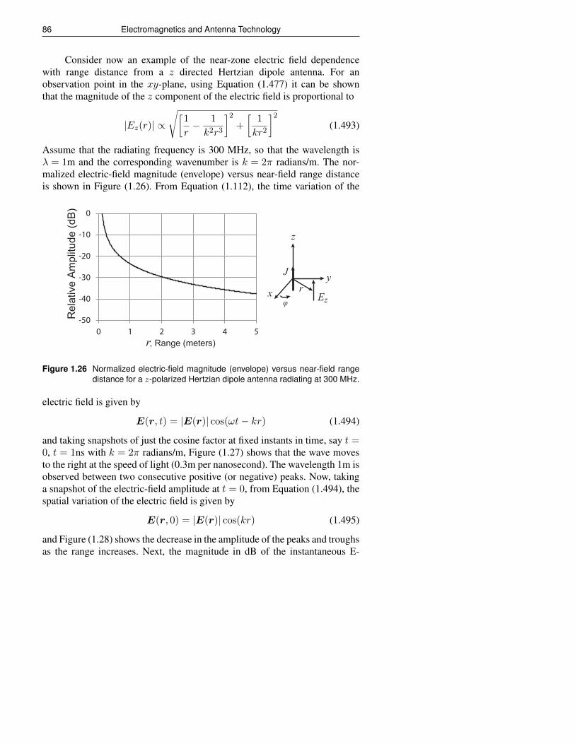
86 Electromagnetics and Antenna Technology
Consider now an example of the near-zone electric field dependencewith range distance from a z directed Hertzian dipole antenna. For anobservation point in the xy-plane, using Equation (1.477) it can be shownthat the magnitude of the z component of the electric field is proportional to
|Ez(r)| ∝
√[1
r− 1
k2r3
]2
+
[1
kr2
]2
(1.493)
Assume that the radiating frequency is 300 MHz, so that the wavelength isλ = 1m and the corresponding wavenumber is k = 2π radians/m. The nor-malized electric-field magnitude (envelope) versus near-field range distanceis shown in Figure (1.26). From Equation (1.112), the time variation of the
-50
-40
-30
-20
-10
0
0 1 2 3 4 5
Rel
ativ
e A
mpl
itude
(dB
)
r, Range (meters)
Ez
J
xy
z
ᵠr
Figure 1.26 Normalized electric-field magnitude (envelope) versus near-field rangedistance for a z-polarized Hertzian dipole antenna radiating at 300 MHz.
electric field is given by
E(r, t) = |E(r)| cos(ωt− kr) (1.494)
and taking snapshots of just the cosine factor at fixed instants in time, say t =0, t = 1ns with k = 2π radians/m, Figure (1.27) shows that the wave movesto the right at the speed of light (0.3m per nanosecond). The wavelength 1m isobserved between two consecutive positive (or negative) peaks. Now, takinga snapshot of the electric-field amplitude at t = 0, from Equation (1.494), thespatial variation of the electric field is given by
E(r, 0) = |E(r)| cos(kr) (1.495)
and Figure (1.28) shows the decrease in the amplitude of the peaks and troughsas the range increases. Next, the magnitude in dB of the instantaneous E-
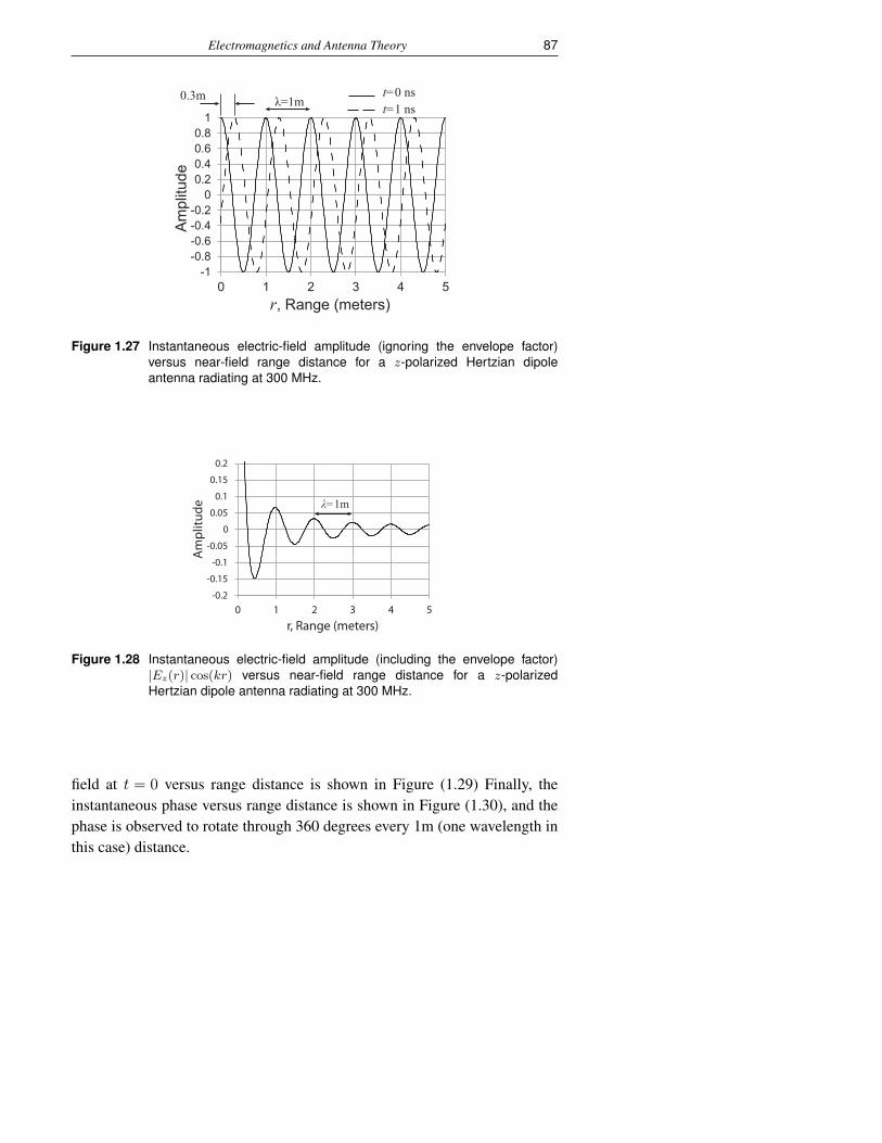
Electromagnetics and Antenna Theory 87
-1-0.8-0.6-0.4-0.2
00.20.40.60.8
1
0 1 2 3 4 5
Am
plitu
de
r, Range (meters)
λ=1mt=0 nst=1 ns
0.3m
Figure 1.27 Instantaneous electric-field amplitude (ignoring the envelope factor)versus near-field range distance for a z-polarized Hertzian dipoleantenna radiating at 300 MHz.
-0.2
-0.15
-0.1
-0.05
0
0.05
0.1
0.15
0.2
0 1 2 3 4 5
Am
plitu
de
r, Range (meters)
λ=1m
Figure 1.28 Instantaneous electric-field amplitude (including the envelope factor)|Ez(r)| cos(kr) versus near-field range distance for a z-polarizedHertzian dipole antenna radiating at 300 MHz.
field at t = 0 versus range distance is shown in Figure (1.29) Finally, theinstantaneous phase versus range distance is shown in Figure (1.30), and thephase is observed to rotate through 360 degrees every 1m (one wavelength inthis case) distance.
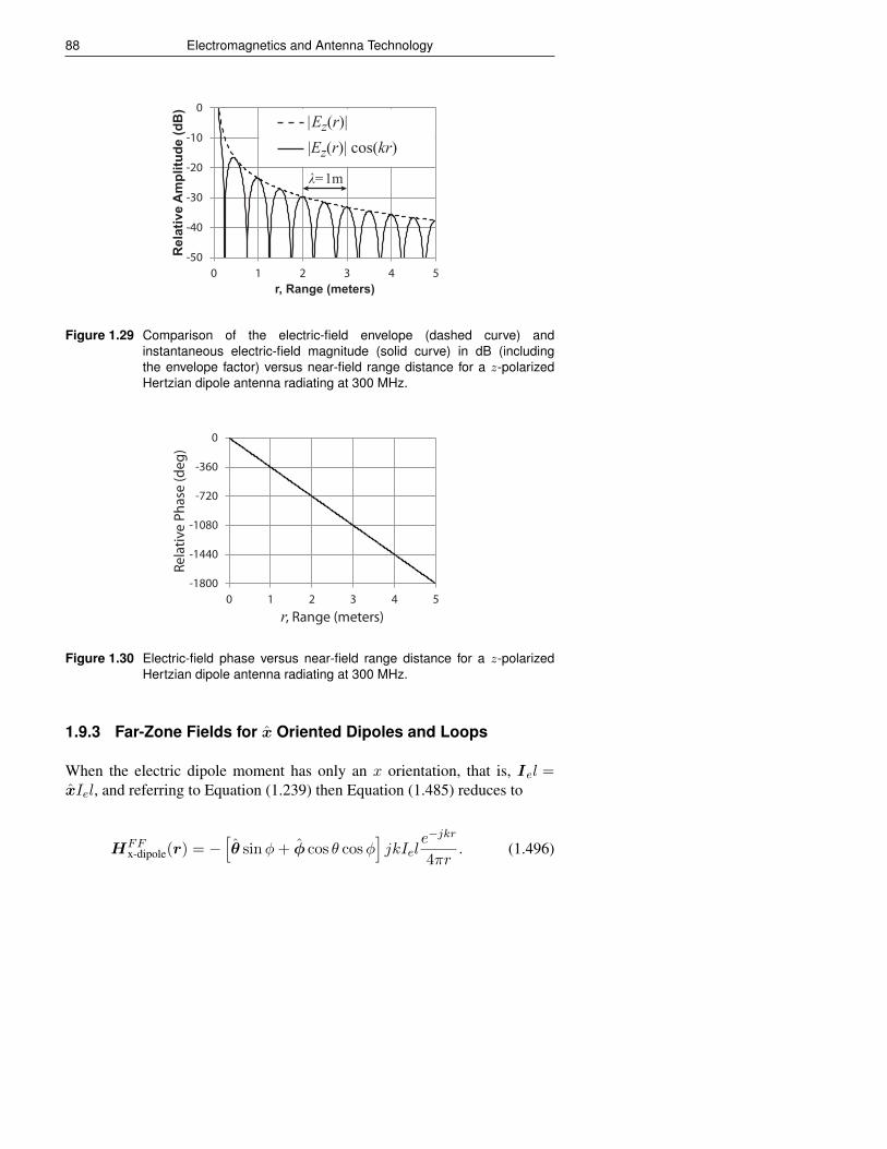
88 Electromagnetics and Antenna Technology
-50
-40
-30
-20
-10
0
0 1 2 3 4 5
Rel
ativ
e A
mpl
itude
(dB
)
r, Range (meters)
|Ez(r)| cos(kr)|Ez(r)|
λ=1m
Figure 1.29 Comparison of the electric-field envelope (dashed curve) andinstantaneous electric-field magnitude (solid curve) in dB (includingthe envelope factor) versus near-field range distance for a z-polarizedHertzian dipole antenna radiating at 300 MHz.
-1800
-1440
-1080
-720
-360
0
0 1 2 3 4 5
Rela
tive
Phas
e (d
eg)
r, Range (meters)
Figure 1.30 Electric-field phase versus near-field range distance for a z-polarizedHertzian dipole antenna radiating at 300 MHz.
1.9.3 Far-Zone Fields for x Oriented Dipoles and Loops
When the electric dipole moment has only an x orientation, that is, Iel =xIel, and referring to Equation (1.239) then Equation (1.485) reduces to
HFFx-dipole(r) = −
[θ sinφ+ φ cos θ cosφ
]jkIel
e−jkr
4πr. (1.496)

Electromagnetics and Antenna Theory 89
Then, applying Equation (1.400), φ× r = θ, and θ × r = −φ yields
EFFx-dipole(r) =
[−θ cos θ cosφ+ φ sinφ
]jkIelη
e−jkr
4πr. (1.497)
By applying duality, the loop fields are given by
HFFx-loop(r) =
[θ cos θ cosφ− φ sinφ
]k2IA
e−jkr
4πr. (1.498)
EFFx-loop(r) = −
[θ sinφ+ φ cos θ cosφ
]ηk2IA
e−jkr
4πr. (1.499)
1.9.4 Far-Zone Fields for y Oriented Dipoles and Loops
When the electric dipole moment has only a y orientation, that is, Iel = yIel,and referring to Equation (1.240) then Equation (1.485) reduces to
HFFy-dipole(r) =
[θ cosφ− φ cos θ sinφ
]jkIel
e−jkr
4πr. (1.500)
Then, applying Equation (1.400), φ× r = θ, and θ × r = −φ yields
EFFy-dipole(r) = −
[θ cos θ sinφ+ φ cosφ
]jkηIelη
e−jkr
4πr. (1.501)
By applying duality, the loop fields are given by
HFFy-loop(r) =
[θ cos θ sinφ+ φ cosφ
]k2IA
e−jkr
4πr. (1.502)
EFFy-loop(r) =
[θ cosφ− φ cos θ sinφ
]ηk2IA
e−jkr
4πr. (1.503)
1.9.5 Image Theory for Electric and Magnetic Dipole Antennas
Image theory can be used to compute the fields caused by an electric dipoleor a magnetic dipole (electric current loop) over a perfect electric conductoras depicted in Figure 1.15. The sign of the image can be determined by usingthe exact electric field expresssions (as given in the previous section) for theelectric dipole and magnetic dipole and by enforcing boundary conditions thatthe total tangential electric field be zero at the surface of the perfect electricconductor. A horizontal electric dipole will have a negative image, whereas ahorizontal magnetic dipole will have a positive image. Additionally, a vertical
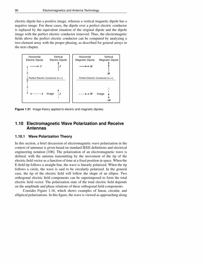
90 Electromagnetics and Antenna Technology
electric dipole has a positive image, whereas a vertical magnetic dipole has anegative image. For these cases, the dipole over a perfect electric conductoris replaced by the equivalent situation of the original dipole and the dipoleimage with the perfect electric conductor removed. Thus, the electromageticfields above the perfect electric conductor can be computed by analyzing atwo-element array with the proper phasing, as described for general arrays inthe next chapter.
J
h
Horizontal Electric Dipole
VerticalElectric Dipole
Image−
M
Horizontal Magnetic Dipole
VerticalMagnetic Dipole
−
Perfect Electric Conductor (σ=∞)Perfect Electric Conductor (σ=∞)
Image
h
J
JJ
M
M
M
Figure 1.31 Image theory applied to electric and magnetic dipoles.
1.10 Electromagnetic Wave Polarization and ReceiveAntennas
1.10.1 Wave Polarization Theory
In this section, a brief discussion of electromagnetic wave polarization in thecontext of antennas is given based on standard IEEE definitions and electricalengineering notation [106]. The polarization of an electromagnetic wave isdefined, with the antenna transmitting by the movement of the tip of theelectric field vector as a function of time at a fixed position in space. When theE-field tip follows a straight line, the wave is linearly polarized. When the tipfollows a circle, the wave is said to be circularly polarized. In the generalcase, the tip of the electric field will follow the shape of an ellipse. Twoorthogonal electric field components can be superimposed to form the totalelectric field vector. The polarization state of the total electric field dependson the amplitude and phase relations of these orthogonal field components.
Consider Figure 1.16, which shows examples of linear, circular, andelliptical polarizations. In this figure, the wave is viewed as approaching along
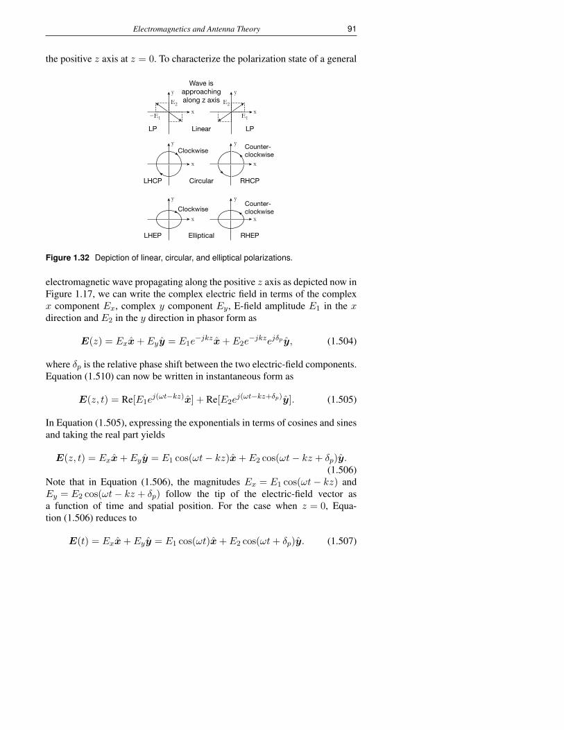
Electromagnetics and Antenna Theory 91
the positive z axis at z = 0. To characterize the polarization state of a general
LP
LHCP
Clockwise
LHEP
LP
RHCP
Counter-clockwise
RHEP
Wave isapproachingalong z axis
Linear
Circular
Elliptical
ClockwiseCounter-clockwise
−E1
E2 E2
E1
y
y
y
x x
x x
x x
y
y
y
Figure 1.32 Depiction of linear, circular, and elliptical polarizations.
electromagnetic wave propagating along the positive z axis as depicted now inFigure 1.17, we can write the complex electric field in terms of the complexx component Ex, complex y component Ey, E-field amplitude E1 in the xdirection and E2 in the y direction in phasor form as
E(z) = Exx+ Eyy = E1e−jkzx+ E2e
−jkzejδp y, (1.504)
where δp is the relative phase shift between the two electric-field components.Equation (1.510) can now be written in instantaneous form as
E(z, t) = Re[E1ej(ωt−kz)x] + Re[E2e
j(ωt−kz+δp)y]. (1.505)
In Equation (1.505), expressing the exponentials in terms of cosines and sinesand taking the real part yields
E(z, t) = Exx+ Eyy = E1 cos(ωt− kz)x+ E2 cos(ωt− kz + δp)y.(1.506)
Note that in Equation (1.506), the magnitudes Ex = E1 cos(ωt− kz) andEy = E2 cos(ωt− kz + δp) follow the tip of the electric-field vector asa function of time and spatial position. For the case when z = 0, Equa-tion (1.506) reduces to
E(t) = Exx+ Eyy = E1 cos(ωt)x+ E2 cos(ωt+ δp)y. (1.507)

92 Electromagnetics and Antenna Technology
τp
εP
OA
OB
x
y γp
x
y
B
A
O
Minor axisMajor axis
E2
E
E E1
Figure 1.33 Depiction of the general tilted polarization ellipse.
Referring to Figure 1.17, the angle γp is expressed in terms of E1 andE2 as
γp = tan−1 E2
E1. (1.508)
In Equation (1.508) we note that E1 and E2 are peak values and thus 0 ≤γp ≤ 90. Furthermore, note that
|E| = E·E∗ = |Ex|2 + |Ey|2 = |E1|2 + |E2|2. (1.509)
At z = 0, Equation (1.510) reduces to
E(z = 0) = Exx+ Eyy = E1x+ E2ejδp y, (1.510)
Further, note that the amplitudes E1 = |E| cos γp and E2 = |E| sin γp, andthen the electric field unit vector can be expressed as
e =E
|E|=E1
|E|x+
E2
|E|y (1.511)
which reduces toe = cos γpx+ sin γpe
jδp y. (1.512)
For the case with z = 0, it is observed that Equation (1.510) can also beexpressed as
E(γp, δp) =√E2
1 + E22(cos γpx+ sin γpe
jδp y) = |E|e. (1.513)
In Equation (1.513), e is the complex unit vector polarization state of theelectromagnetic wave.
Electromagnetics and Antenna Theory 93
It is worth noting that the more general case of spherical coordinates fora plane wave propagating in the radial direction r can be expressed as
E(r) = Eθθ + Eφφ = E1e−jkrθ + E2e
−jkrejδpφ, (1.514)
For the case with r = 0, it is observed that Equation (1.514) can be expressedas
E(γp, δp) =√E2
1 + E22(cos γpθ + sin γpe
jδpφ) = |E|e. (1.515)
Now for an incident plane wave propagating in the negative radialdirection, note that the cross product of the unit vectors for theta and phi gives
θ × φ = −r (1.516)
If we compare φwith x and θ with y in Figure 1.33 and with Equation (1.512)then it follows that the incident wave electric-field unit vector einc or incidentpolarization unit vector pinc in spherical coordinates is given by
einc = pinc =Eθ|E|
θ +Eφ|E|
φ = sin γpejδp θ + cos γpφ. (1.517)
Referring now to the upper left diagram of Figure 1.16, the wave shownis slanted to the left, and it is linearly polarized. In contrast, in the upper rightdiagram of Figure 1.16, the linearly polarized wave is slanted to the right. Forcircularly polarized (CP) waves, the amplitude of the two orthogonal electricfield components will be equal, that is, E1 = E2, and the relative phase willbe δp = ±90. By the IEEE definition, for a left-hand CP wave approaching,the relative phase will be δp = 90 and the tip of the electric field vector willrotate clockwise as in the middle-left diagram in Figure 1.16. For a right-handCP wave approaching, δp = −90, and the tip will rotate counter-clockwiseas in the middle-right diagram in Figure 1.16.
For elliptically polarized (EP) waves, the amplitudes E1 and E2 will notbe equal. If the relative phase is δp = 90, then the wave will be left-handelliptically polarized (LHEP) with the major axis along the x-axis (lower leftdiagram in Figure 1.16). If the relative phase is δp = −90, then the wavewill be right-hand elliptically polarized (RHEP) with the major axis alsoalong the x-axis (lower right diagram in Figure 1.16). For general ellipticallypolarized waves, the relative phase δp will vary over ±180. The ellipticalpolarization will be right-handed for−180 < δp < 0 and will be left-handedfor 0 < δp < 180.
For the general case of an elliptically polarized wave [106], thepolarization ellipse major axis will tilt away at the angle τp from the x axis
94 Electromagnetics and Antenna Technology
as depicted in Figure 1.17. In Figure 1.17, the ratio of the major axis to theminor axis is defined as the axial ratio (AR), that is,
AR = ±OAOB
. (1.518)
The sign of the axial ratio is positive for right-hand polarization and negativefor left-hand polarization [106, p. 38]. The magnitude of the axial ratio variesfrom 1 to infinity, that is, 1 ≤ |AR| ≤ ∞. The polarization ellipticity angle,denoted εp, is expressed as
εp = cot−1(−AR). (1.519)
In decibels, the axial ratio is expressed as
ARdB = 20 log10 |AR|. (1.520)
The polarization state of a general electromagnetic wave can becompletely specified by either the pair of angles (εp, τp) or (γp, δp). Thetransformation of the angles (εp, τp) to (γp, δp) is given by
γp =1
2cos−1(cos 2εp cos 2τp) (1.521)
δp = tan−1 tan 2εpsin 2τp
. (1.522)
In Equation (1.522), the angle 2τp represents longitude and 2εp representslatitude for a point on a sphere known as the Poincaré sphere [106].
Consider now the polarization efficiency (or antenna-wave coupling)between transmit and receive linearly polarized antennas as depicted inFigure 1.18. The transmit antenna produces the incident linear polarizationdenoted pinc.
The polarization efficiency ηp is expressed as the magnitude squaredof the dot product of the unit vectors for the incident linear polarization andcomplex conjugate of the receiving antenna’s unit vector polarization definedunder transmitting conditions (denoted pa), that is,
ηp = |pinc·p∗a |2 = cos2 ψ (1.523)
where ψ is the projected angle between the associated transmit and receivelinear-polarized antenna unit vectors, and the complex conjugate is requiredto take account of the relative coordinate systems for the incident field andthe receive antenna (the propagation directions are opposite). That is, the
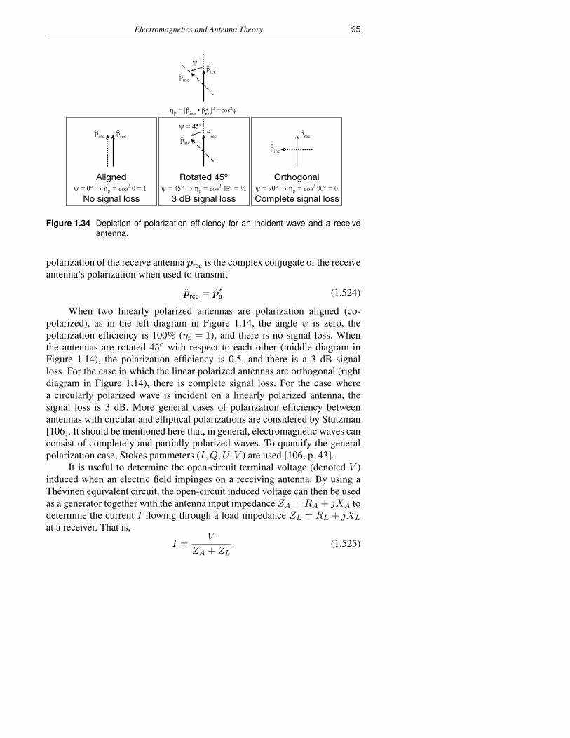
Electromagnetics and Antenna Theory 95
Aligned
No signal loss
Rotated 45º
3 dB signal loss
Orthogonal
Complete signal lossψ = 0° → ηp = cos2 0 = 1
pinc^ prec
^pinc^
prec^
pinc^
prec^
ηp = |pinc • prec|2 =cos2ψ ^^ *
ψ = 45°
ψ = 45° → ηp = cos2 45° = ½
ψ = 90° → ηp = cos2 90° = 0
pinc^
prec^
ψ
Figure 1.34 Depiction of polarization efficiency for an incident wave and a receiveantenna.
polarization of the receive antenna prec is the complex conjugate of the receiveantenna’s polarization when used to transmit
prec = p∗a (1.524)
When two linearly polarized antennas are polarization aligned (co-polarized), as in the left diagram in Figure 1.14, the angle ψ is zero, thepolarization efficiency is 100% (ηp = 1), and there is no signal loss. Whenthe antennas are rotated 45 with respect to each other (middle diagram inFigure 1.14), the polarization efficiency is 0.5, and there is a 3 dB signalloss. For the case in which the linear polarized antennas are orthogonal (rightdiagram in Figure 1.14), there is complete signal loss. For the case wherea circularly polarized wave is incident on a linearly polarized antenna, thesignal loss is 3 dB. More general cases of polarization efficiency betweenantennas with circular and elliptical polarizations are considered by Stutzman[106]. It should be mentioned here that, in general, electromagnetic waves canconsist of completely and partially polarized waves. To quantify the generalpolarization case, Stokes parameters (I,Q, U, V ) are used [106, p. 43].
It is useful to determine the open-circuit terminal voltage (denoted V )induced when an electric field impinges on a receiving antenna. By using aThevinen equivalent circuit, the open-circuit induced voltage can then be usedas a generator together with the antenna input impedance ZA = RA + jXA todetermine the current I flowing through a load impedance ZL = RL + jXL
at a receiver. That is,
I =V
ZA + ZL. (1.525)
96 Electromagnetics and Antenna Technology
Note that the real part of the antenna input impedance is equal to the antennaradiation resistance (denoted Rr), that is, RA = Rr. The time-average powerPL delivered to the receiver, in terms of the resistive component RL of thereceiver load impedance, is given by
PL =1
2|I|2RL =
1
2|V |2 RL|ZA + ZL|2
(1.526)
and the complex voltage across the receiver load is given by
Vrec = VZL
ZA + ZL. (1.527)
Utilizing the generalized antenna vector effective height (h), which has unitsof meters, the induced open-circuit voltage across the terminals of an antennais given by
V = Einc·h∗ (1.528)
whereh = hpa (1.529)
and where h is the magnitude of the vector effective height. Now express theincident electric field Einc with magnitiude Eo, phase ψo, with polarizationpinc as
Einc = Eoeψo pinc. (1.530)
A few examples of the induced open-circuit voltage given by Equation (1.528)will now be considered.
Assume 45 slant-left and 45 slant-right linearly-polarized shortdipoles oriented in the yz-plane such that
pslant left =−y + z√
2(1.531)
pslant right =y + z√
2(1.532)
Assume plane wave incidence with vertical polarization at the arbitraryposition (x, y, z) as
Evinc = θEiθ(x, y, z) (1.533)
or horizontal polarization as
Ehinc = φEiφ(x, y, z) (1.534)
Electromagnetics and Antenna Theory 97
Substituting Equations (1.531), (1.532), (1.533), and (1.534) in Equa-tion (1.528) yields
V vslant left = Eiθ(x, y, z)θ ·
[−y + z√2
](1.535)
V vslant right = Eiθ(x, y, z)θ ·
[y + z√
2
](1.536)
V hslant left = Eiφ(x, y, z)φ ·
[−y + z√2
](1.537)
V hslant right = Eiφ(x, y, z)φ ·
[y + z√
2
](1.538)
From Equations (1.237) and (1.238) and referring to Figure 2.4 it follows forsource incidence angles θ = θi and φ = φi that
θ·y = cos θi sinφi (1.539)
θ·z = − sin θi (1.540)
φ·y = cosφi (1.541)
φ·z = 0 (1.542)
It follows then that
V vslant left = −Eiθ(x, y, z)
[cos θi sinφi + sin θi√
2
](1.543)
V vslant right = −Eiθ(x, y, z)
[cos θi sinφi − sin θi√
2
](1.544)
V hslant left = −Eiφ(x, y, z)
cosφi√2
(1.545)
V hslant right = Eiφ(x, y, z)
cosφi√2
(1.546)
For plane-wave incidence with wavenumber k = 2π/λ at an arbitrary nthposition (xn, yn, zn), the electric field has a constant amplitude and a phasethat varies as
Ψi = k sin θi(xn cosφi + yn sinφi) + kzn cos θi (1.547)
98 Electromagnetics and Antenna Technology
and the complex electric field is then
Ei(k, xn, yn, zn, θi, φi) = ejk[sin θi(xn cosφi+yn sinφi)+zn cos θi] (1.548)
It follows from Equations (1.523) and (1.528) that
|V | = Eoh|pinc·p∗a | = Eoh√ηp. (1.549)
Substituting Equation (1.549) in Equation (1.526) yields
PL =1
2|V |2 RL|ZA + ZL|2
=1
2E2oh
2ηpRL
|ZA + ZL|2. (1.550)
In the case where the receive antenna is connected to a conjugate-matched load impedance (ZL = RA − jXA), it follows from Equation (1.550)that the time-average power transferred to the resistive part (RA) of thereceiver load is given by
PL =1
2
|V |2
4RA=
1
8RAE2oh
2ηp. (1.551)
Now the magnitude of the time-average power density (denoted S) incidenton an antenna in free space is given by
S =1
2
E2o
ηo(1.552)
where ηo is the impedance of free space. Next, in terms of effective receiveaperture (denoted Aeff), the time-average received power at the conjugate-matched load can be expressed as
PL = ηpSAeff = ηp1
2
E2o
ηoAeff. (1.553)
Now, setting Equation (1.551) equal to Equation (1.553) yields
h = 2
√RAηoAeff (1.554)
which is a general expression for the effective height of an antenna assuminga conjugate matched load. Solving Equation (1.554) for the effective aperturegives
Aeff =h2ηo4RA
. (1.555)

Electromagnetics and Antenna Theory 99
Note, in the literature, the electric antenna factor (denoted AFe) with unitsof 1/m is often used to convert the incident electric field magnitude (Eo) toreceived voltage magnitude, that is,
|V | = EoAFe
, (1.556)
and it follows that the electric antenna factor and effective antenna height arerelated as
AFe =1
h. (1.557)
Additionally, in the literature, the magnetic antenna factor (denoted AFm)with units of 1/m is often used to convert the incident magnetic fieldmagnitude (Ho) to received voltage magnitude, that is,
|V | = Ho
AFm, (1.558)
and it follows that the magnetic antenna factor and magnetic effective antennaheight are related as
AFm =1
hm. (1.559)
To quantify the maximum effective area given by Equation (1.555), itis necessary to determine the radiation resistance Rr, or equivalently theinput resistance RA, for the antenna of interest, as discussed below for theshort dipole and small loop antenna. Since an antenna can be treated as aload, the radiation resistance can be determined by quantifying the time-average radiated power (denoted Pave) or equivalently the time-average powerdelivered to the antenna, and using the relation
Prad =1
2I2oRr (1.560)
and solving for Rr as
Rr =2Prad
I2o
. (1.561)
Now the time-average radiated power can be found by integrating the time-average power density over the volume surrounding the antenna as the rangedistance tends to infinity, that is,
Prad =
∫ 2π
0
∫ π
0r·1
2Re[E×H∗]r2 sin θdθdφ. (1.562)
100 Electromagnetics and Antenna Technology
Repeating the general far-field Equations (1.279) and (1.282), we have
EFF = −jωµe−jkr
4πr(θfθ + φfφ) (1.563)
HFF = −jk e−jkr
4πr(φfθ − θfφ). (1.564)
To compute the far-zone electric (EFF) and magnetic (HFF) fields, it isnecessary to determine the vector current moment f(θ, φ) for the antennaof interest.
1.10.2 Short Dipole Receive Characteristics
For an electrically short dipole with total length l in free space, the currentdistribution has a triangular shape [121]. The maximum effective height isdetermined by integrating the current over the dipole physical length dividedby the terminal current Io [1, p. 31], and for symmetrical currents,
h =1
Io
∫ l2
− l2
I(z′)dz′ =2
Io
∫ l2
0I(z′)dz′. (1.565)
A triangular current distribution is a good approximation for short dipoles oftotal length l, that is,
I(z′) =2Iol
[l
2− |z′|
]. (1.566)
Substituting Equation (1.566) in Equation (1.565) and integrating, theeffective height is found to be equal to one-half the physical length of theshort dipole with triangular current, that is,
hdipole =1
2l. (1.567)
Thus, the open-circuit voltage induced in a short dipole is determined bysubstituting Equation (1.567) into Equation (1.549) with the result (ignoringthe radiation pattern) ∣∣Vdipole
∣∣ =1
2Eol√ηp. (1.568)
For the short dipole, the far-zone electric and magnetic fields can bedetermined from the vector current moment given by Equation (1.269), andusing Equation (1.566) for the triangular current distribution, it follows that
J(r′) = zI(z′)δ(x′)δ(y′) = z2Iol
[l
2− |z′|
]δ(x′)δ(y′). (1.569)
Electromagnetics and Antenna Theory 101
Now, using Equations (1.236) and (1.241), it follows from Equation (1.269)that for the triangular current distribution that the vector current moment is
f(θ, φ) =
∫VJ(r′)ejkr·r′ dv′ = −θ2Io
lsin θ
∫ l2
− l2
[l
2− |z′|
]ejkz
′ cos θdz′
(1.570)where the only nonradial component in this case is the θ component. For anelectrically short dipole, the phase term in Equation (1.570) can be ignored,and thus the vector current moment for the triangular current distribution isdetermined to be
fθ(θ) = − l2Io sin θ. (1.571)
Using the above expressions given by Equations ( 1.562), (2.33), (1.564), and(1.571) the radiated power is now determined as
Prad = 2π
[ηk2
(4π)2
]1
2
∫ π
0|fθ|2 sin θdθ = π
[120πk2
(4π)2
]l2I2
o
4
∫ π
0sin3 θdθ
(1.572)and noting that ∫ π
0sin3 θdθ =
4
3, (1.573)
it follows that the power radiated in watts is
Pdipole, triangular currentrad =
5
2(kl)2I2
o . (1.574)
Thus, the radiation resistance of a short dipole with triangular currentdistribution is
Rdipole, triangular currentr =
2Prad
I2o
= 5(kl)2. (1.575)
Substituting Equations (1.567) and (1.575) in Equation (1.555) yields theeffective area of a short dipole with triangular current as
Adipole, triangular currenteff =
h2ηo4RA
=l2
4 120π
4 · 5(kl)2=
3λ2
8π≈ λ2
8. (1.576)
1.10.3 Small Current Loop Receive Characteristics
Consider now an N -turn loop antenna of arbitrary shape with physical areaA illuminated by a uniform magnetic flux density with magnitude Bo =µoHo, where µo is the permeability of free space and Ho is the magnitude
102 Electromagnetics and Antenna Technology
of the magnetic field. The magnitude of the open-circuit voltage is readilydetermined, according to the time rate of change of magnetic flux densitythrough the loop, using Faraday’s law in time-harmonic form as∣∣Vloop
∣∣ =∣∣−jωANBo√ηp∣∣ = ωANµoHo
√ηp. (1.577)
For a plane wave, Ho = Eo/ηo, where ηo is the impedance of free space, andnoting ωµo/ηo = k = 2π/λ, it follows that the open-circuit voltage of theloop is ∣∣Vloop
∣∣ = ANωµoηo
Eo√ηp = ANkEo
√ηp (1.578)
and so setting Equation (1.578) equal to Equation (1.549), the maximumeffective height of an N -turn loop antenna with physical area A is
hloop = ANk. (1.579)
In the case of an N -turn small loop antenna with uniform current, fromEquations (1.490) and (1.491), the far-zone fields are
HFFz-loop, N turns(r) = −θk2NIA
e−jkr
4πrsin θ (1.580)
EFFz-loop, N turns(r) = φNIAωµk
e−jkr
4πrsin θ. (1.581)
Substituting Equations (6.11) and (6.12) in Equation (1.562) and evaluatingthe integral yields the radiated power
Ploop, uniform currentrad = 10(k2NA)2I2
o . (1.582)
Thus, the radiation resistance of an N -turn loop antenna with uniform currentdistribution and physical area A is
Rloop, uniform currentr =
2Prad
I2o
= 20(k2NA)2. (1.583)
Substituting Equations (1.589) and (1.583) in Equation (1.555) yields theeffective area of an N -turn small loop antenna with uniform current as
Aloop, uniform currenteff =
h2ηo4RA
=(ANk)2120π
4 · 20(k2NA)2=
3λ2
8π≈ λ2
8, (1.584)
and this result is identical to the result obtained for the short dipole (seeEquation (1.576).
Electromagnetics and Antenna Theory 103
1.10.4 Ferrite-Loaded Small Current Loop ReceiveCharacteristics
Consider now a ferrite-loaded N -turn loop antenna [20]with physical area Ailluminated by a uniform magnetic flux density with magnitude Bo = µoHo,where µo is the permeability of free space and Ho is the magnitude of themagnetic field in free space. The N -turn loop is assumed to be wound arounda uniform ferrite core with relative intrinsic permeability of the unboundedferrite material denoted as µri ferrite core. The relative effective permeability ofthe ferrite core is denoted as µre ferrite core, which is related to µri ferrite core as
µre ferrite core =µri ferrite core
1 +D(µri ferrite core − 1)(1.585)
where D is the static demagnetization factor. The static demagnetizationfactor is geometry dependent, and for an ellipsoidal core with length L andradius a (where L >> a), D is given by
D =
(2a
L
)2 [ln
(L
a
)− 1
](1.586)
The presence of the ferrite material increases the amplitude of the incidentmagnetic field and open-circuit voltage linearly by the relative effectivepermeability of the ferrite core as [20]
Ho ferrite core = µre ferrite coreHo (1.587)
and from Equation (1.578)∣∣Vloop∣∣ = ANkµre ferrite coreEo
√ηp (1.588)
and so setting Equation (1.588) equal to Equation (1.549), the maximumeffective height of an N -turn ferrite loop antenna with physical area A is
hloop = ANkµre ferrite core. (1.589)
The radiation resistance of an N -turn ferrite-loaded loop antenna, withuniform current distribution and physical area A, increases by the square ofthe relative effective permeability of the ferrite and is given by
Rferrite loop, uniform currentr =
2Prad
I2o
= 20(k2NA)2µ2re ferrite core (1.590)
or in terms of loop circumference C using A = C2/(4π) as
Rferrite loop, uniform currentr = 20π2
(C
λ
)4
N2µ2re ferrite core. (1.591)

104 Electromagnetics and Antenna Technology
1.11 Bandwidth and Quality Factor
1.11.1 Introduction
Bandwidth (B) is defined as the difference between the highest f2 and lowestf1 operating frequencies, that is,
B = f2 − f1 = ∆f. (1.592)
The terms highest and lowest operating frequencies usually refer to the radaror communications system meeting some desired performance metric, suchas radiation pattern, gain, beamwidth, sidelobe level, reflection coefficient orVSWR, transmit power level, sensitivity, and so on. In specifying a bandwidthvalue, sometimes the −3 dB point is used, and sometimes a different level,say the −10 dB point, is used; hence, it is important to define what is meantby bandwidth. Fractional bandwidth (FBW) is defined as the ratio of thebandwidth to the arithmetic mean center frequency fc, that is,
FBW =f2 − f1
fc=
∆f
fc. (1.593)
The percent bandwidth (PBW) is computed as
PBW = FBW× 100% =∆f
fc× 100%. (1.594)
The ratio bandwidth (RBW) is defined as the ratio of the highest operatingfrequency to the lowest operating frequency, or
RBW =f2
f1. (1.595)
Antennas that have ultrawideband (or wideband) characteristics have numer-ous applications [80–93]. To quantify the bandwidth, consider an ultrawide-band system that requires an antenna to operate from 30 to 3000 MHz. Itfollows that the bandwidth B = 2700 MHz, the FBW = (3000− 30)/1515 =1.96, the PBW = 196%, and the RBW = 3000 / 30 = 100. In the limit asthe bandwidth grows linearly, the FBW approaches 2, the PBW approaches200%, and the RBW grows linearly. Each of the bandwidth definitions areuseful and are applied as appropriate to the desired application.
Bandwidth is important in radar systems requiring fine range resolution.The time t it takes for an electromagnetic wave to travel a range distance rbetween two points in free space is fundamentally related to the speed of lightc (measured value c = 2.99792458× 10⁸ m/s ≈ 3.0× 10⁸ m/s) as
t =r
c. (1.596)
Electromagnetics and Antenna Theory 105
The wavelength of an electromagnetic wave in free space is expressed as
λ =c
f(1.597)
where f is the frequency of the wave. In a radar system application, the rangeresolution ∆r in free space is given in terms of the radar pulse width τ as [47]
∆r =cτ
2. (1.598)
Since the bandwidth of the radar pulse is inversely proportional to the pulsewidth, that is,
B =1
τ(1.599)
it follows that the range resolution can also be expressed as
∆r =c
2B. (1.600)
For example, a 1 µs pulse width has a bandwidth of 1 MHz; thus, the rangeresolution is computed from Equation (1.600) to be 150 m. Similarly, a 10 nspulse width has a bandwidth of 100 MHz, which corresponds to a rangeresolution of 1.5 m. In the case of an ultrawideband pulse with a bandwidthon the order of gigahertz, the range resolution is on the order of centimetersand Equation (1.600) can be written conveniently as
∆rcm =30
2BGHz
. (1.601)
Thus, a radar with a pulse width of 1 ns, which has a bandwidth of 1 GHz,will have a range resolution of
∆r =30 cm
2= 15 cm ≈ 6 inches. (1.602)
The terms ultrawideband[80-93] or wideband are used to refer to an antennathat covers a large frequency range. As there is no standard definition forultrawideband antennas, we simply define that an ultrawideband antenna willhave a PBW typically 25% or more or a RBW of 1.25 or more as described inthe 2007 IEEE Standard for Ultrawideband Radar Definitions [80]. Over thisbandwidth, the antenna will have desired radiation characteristics and will nothave any significant amplitude degradation for the application of interest.
Ultrawideband array performance requirements are highly dependent onthe application [81]. For example, in a receive-only application with a strong
106 Electromagnetics and Antenna Technology
signal, it might only be necessary to provide an antenna with a reflectioncoefficient on the order of−6 dB or better with sufficient pattern gain to closethe link, but for a transmit application, the reflection coefficient requirementmight be on the order of −10 dB or better to avoid significant reflectedsignal toward the transmitter and significant loss in effective isotropic radiatedpower. For ground-penetrating radar or impulse radar applications [81, 82],since targets are at very close range (1 to 2 m), it is important to designthe ultrawideband antenna with sufficient resistive attenuation to avoid signalringing effects [83–85].
The above definitions of bandwidth do not take into account the size ofthe antenna aperture, which affects the time delay for transmitted and receivedsignals. For a transmitted or incident wavefront with either a pulsed, noise,or other wideband spectrum, the phased array design and analysis must takeinto account the time delay as will be described in the next chapter. The nextsection quantifies bandwidth in terms of the antenna input impedance andquality factor Q.
1.11.2 Derivation of Q Factor from Input Impedance
The impedance bandwidth for an allowed value of VSWR of an antenna canbe computed from a quantity known as the quality factor that depends on thereactance and radian frequency derivatives of the resistance and reactance.The so-called quality factor (denoted Q(ω) for an antenna tuned to have zeroreactance at the radian frequency ω is defined for example by Yaghjian andBest [99] as
Q(ω) =ω|W (ω)|PA(ω)
(1.603)
where W (ω) is the internal energy and PA is the total power accepted by theantenna. Assume that the antenna has an input impedance expressed as
ZA(ω) = RA(ω) + jXA(ω) (1.604)
whereRA(ω) andXA(ω) are the antenna input resistance and input reactance,respectively. Tuning can be achieved at radian frequency ωo with a seriesreactance, denoted Xs, for either a series inductor Ls or series capacitor Cs tomake the total reactance of an antenna equal to zero at a radian frequency ωo.That is, the total reactance of the antenna plus series reactance is expressedas,
XT (ω) = XA(ω) +Xs(ω) (1.605)
where
Xs(ω) =
ωLs if X(ωo) < 0− 1ωCs
if X(ωo) > 0(1.606)

Electromagnetics and Antenna Theory 107
Yaghjian and Best assume that after the antenna has been tuned at frequencyωo, then the antenna is connected to a transmission line with characteristicimpedance equal to the antenna’s tuned input resistance (denoted Ro). Takingthe derivative of XT (ω) with respect to radian frequency yields
dXT (ω)
dω=
dXA(ω)dω + Ls if X(ωo) < 0
dXA(ω)dω + 1
ω2Csif X(ωo) > 0
(1.607)
which can be written in simplifed form as
dXT (ω)
dω=dXA(ω)
dω+|X(ω)|ω
(1.608)
Now, the power accepted by the antenna is given by
PA(ω) =1
2Re[Vo(ω)I∗o (ω)] (1.609)
where ∗ means complex conjugate. The power accepted by the antenna is alsoexpressed as the sum of the radiated power and any power lost due to thematerial of the antenna as
PA(ω) = Pradiated(ω) + Ploss(ω) (1.610)
The radiated power is quantified by
Pradiated(ω) =1
2|Io(ω)|2Rr(ω) (1.611)
where Rr(ω) is defined as the radiation resistance. The power loss due to anylossy material of the antenna is determined as
Ploss(ω) =1
2|Io(ω)|2Rloss(ω) (1.612)
where Rloss is defined as the loss resistance. Then, applying Maxwell’sequations in a lengthy derivation by Yaghjian and Best [99, Equation 96],an accurate approximate expression for the antenna quality factor (denoted bythe authors as Qz) is given by
QZ =ω
2R(ω)
√[dR(ω)
dω
]2
+
[dX(ω)
dω+
∣∣∣∣X(ω)
ω
∣∣∣∣]2
(1.613)
Furthermore, Yaghjian and Best have shown that another accurate approxi-mate quality factorQB is expressed in terms of allowed VSWR and fractionalbandwidth (FBW) as
QB =VSWR-1
FBW√
VSWR(1.614)
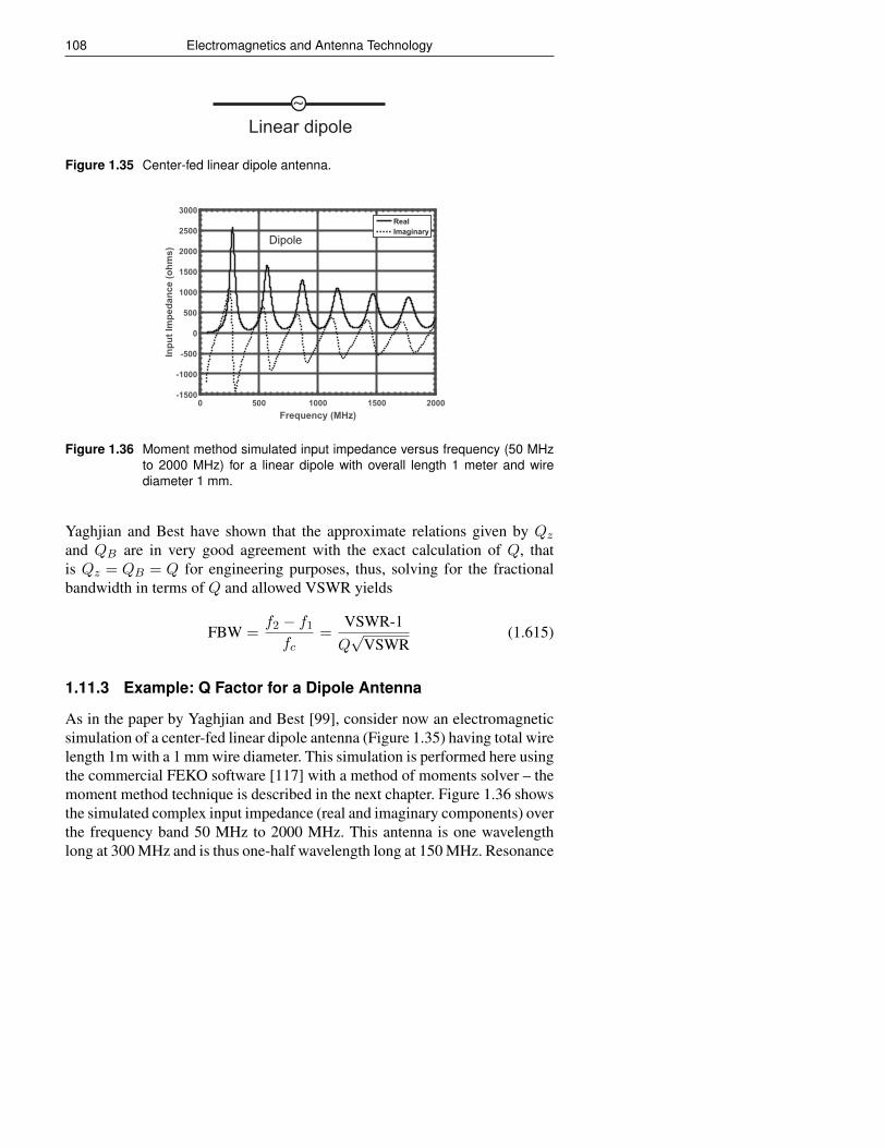
108 Electromagnetics and Antenna Technology
~Linear dipole
Figure 1.35 Center-fed linear dipole antenna.
0 500 1000 1500 2000Frequency (MHz)
-1500
-1000
-500
0
500
1000
1500
2000
2500
3000
Inpu
t Im
peda
nce
(ohm
s)
RealImaginary
Dipole
Figure 1.36 Moment method simulated input impedance versus frequency (50 MHzto 2000 MHz) for a linear dipole with overall length 1 meter and wirediameter 1 mm.
Yaghjian and Best have shown that the approximate relations given by Qzand QB are in very good agreement with the exact calculation of Q, thatis Qz = QB = Q for engineering purposes, thus, solving for the fractionalbandwidth in terms of Q and allowed VSWR yields
FBW =f2 − f1
fc=
VSWR-1Q√
VSWR(1.615)
1.11.3 Example: Q Factor for a Dipole Antenna
As in the paper by Yaghjian and Best [99], consider now an electromagneticsimulation of a center-fed linear dipole antenna (Figure 1.35) having total wirelength 1m with a 1 mm wire diameter. This simulation is performed here usingthe commercial FEKO software [117] with a method of moments solver – themoment method technique is described in the next chapter. Figure 1.36 showsthe simulated complex input impedance (real and imaginary components) overthe frequency band 50 MHz to 2000 MHz. This antenna is one wavelengthlong at 300 MHz and is thus one-half wavelength long at 150 MHz. Resonance
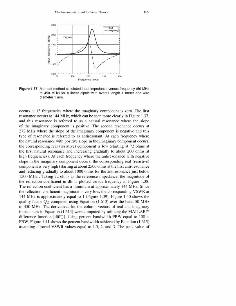
Electromagnetics and Antenna Theory 109
50 150 250 350 450Frequency (MHz)
-2000
-1000
0
1000
2000
3000
Inpu
t Im
peda
nce
(ohm
s)
RealImaginary
Dipole
Figure 1.37 Moment method simulated input impedance versus frequency (50 MHzto 450 MHz) for a linear dipole with overall length 1 meter and wirediameter 1 mm.
occurs at 13 frequencies where the imaginary component is zero. The firstresonance occurs at 144 MHz, which can be seen more clearly in Figure 1.37,and this resonance is referred to as a natural resonance where the slopeof the imaginary component is positive. The second resonance occurs at272 MHz where the slope of the imaginary component is negative and thistype of resonance is referred to as antiresonant. At each frequency wherethe natural resonance with positive slope in the imaginary component occurs,the corresponding real (resistive) component is low (starting at 72 ohms atthe first natural resonance and increasing gradually to about 200 ohms athigh frequencies). At each frequency where the antiresonance with negativeslope in the imaginary component occurs, the corresponding real (resistive)component is very high (starting at about 2500 ohms at the first anti-resonanceand reducing gradually to about 1000 ohms for the antiresonance just below1500 MHz . Taking 72 ohms as the reference impedance, the magnitude ofthe reflection coefficient in dB is plotted versus frequency in Figure 1.38.The reflection coefficient has a minimum at approximately 144 MHz. Sincethe reflection coefficient magnitude is very low, the corresponding VSWR at144 MHz is approximately equal to 1 (Figure 1.39). Figure 1.40 shows thequality factor QZ computed using Equation (1.613) over the band 50 MHzto 450 MHz. The derivatives for the column vectors of real and imaginaryimpedances in Equation (1.613) were computed by utilizing the MATLABTM
difference function [diff()]. Using percent bandwidth PBW equal to 100×FBW, Figure 1.41 shows the percent bandwidth achieved by Equation (1.615)assuming allowed VSWR values equal to 1.5, 2, and 3. The peak value of
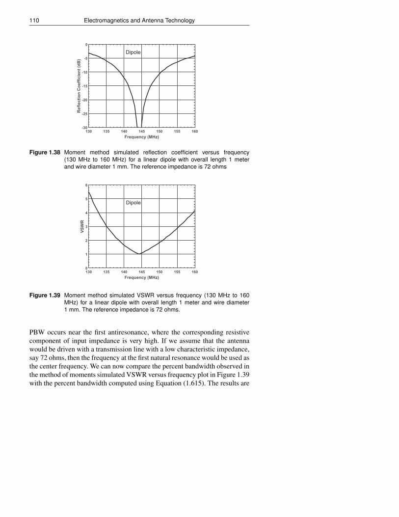
110 Electromagnetics and Antenna Technology
130 135 140 145 150 155 160Frequency (MHz)
-30
-25
-20
-15
-10
-5
0
Ref
lect
ion
Coe
ffici
ent (
dB)
Dipole
Figure 1.38 Moment method simulated reflection coefficient versus frequency(130 MHz to 160 MHz) for a linear dipole with overall length 1 meterand wire diameter 1 mm. The reference impedance is 72 ohms
130 135 140 145 150 155 160Frequency (MHz)
0
1
2
3
4
5
6
VSW
R
Dipole
Figure 1.39 Moment method simulated VSWR versus frequency (130 MHz to 160MHz) for a linear dipole with overall length 1 meter and wire diameter1 mm. The reference impedance is 72 ohms.
PBW occurs near the first antiresonance, where the corresponding resistivecomponent of input impedance is very high. If we assume that the antennawould be driven with a transmission line with a low characteristic impedance,say 72 ohms, then the frequency at the first natural resonance would be used asthe center frequency. We can now compare the percent bandwidth observed inthe method of moments simulated VSWR versus frequency plot in Figure 1.39with the percent bandwidth computed using Equation (1.615). The results are
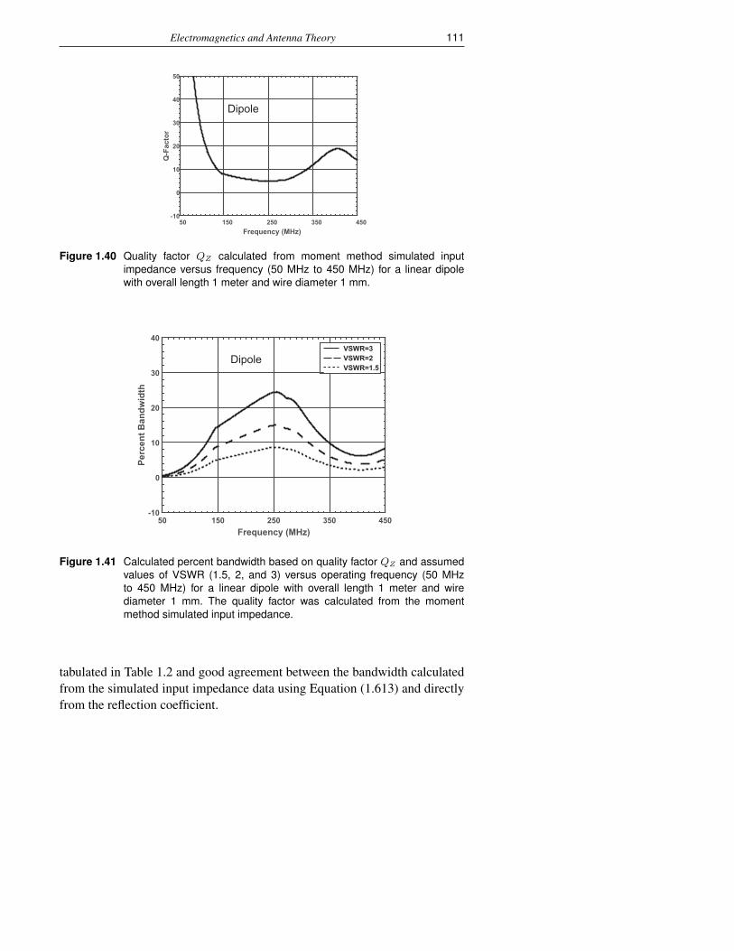
Electromagnetics and Antenna Theory 111
50 150 250 350 450Frequency (MHz)
-10
0
10
20
30
40
50
Q-F
acto
r
Dipole
Figure 1.40 Quality factor QZ calculated from moment method simulated inputimpedance versus frequency (50 MHz to 450 MHz) for a linear dipolewith overall length 1 meter and wire diameter 1 mm.
50 150 250 350 450Frequency (MHz)
-10
0
10
20
30
40
Perc
ent B
andw
idth
VSWR=3VSWR=2VSWR=1.5
Dipole
Figure 1.41 Calculated percent bandwidth based on quality factor QZ and assumedvalues of VSWR (1.5, 2, and 3) versus operating frequency (50 MHzto 450 MHz) for a linear dipole with overall length 1 meter and wirediameter 1 mm. The quality factor was calculated from the momentmethod simulated input impedance.
tabulated in Table 1.2 and good agreement between the bandwidth calculatedfrom the simulated input impedance data using Equation (1.613) and directlyfrom the reflection coefficient.
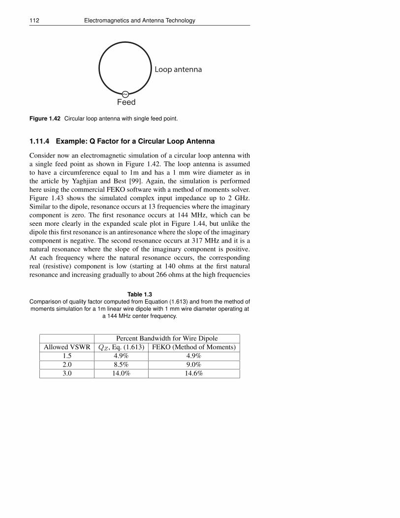
112 Electromagnetics and Antenna Technology
Feed~
Loop antenna
Figure 1.42 Circular loop antenna with single feed point.
1.11.4 Example: Q Factor for a Circular Loop Antenna
Consider now an electromagnetic simulation of a circular loop antenna witha single feed point as shown in Figure 1.42. The loop antenna is assumedto have a circumference equal to 1m and has a 1 mm wire diameter as inthe article by Yaghjian and Best [99]. Again, the simulation is performedhere using the commercial FEKO software with a method of moments solver.Figure 1.43 shows the simulated complex input impedance up to 2 GHz.Similar to the dipole, resonance occurs at 13 frequencies where the imaginarycomponent is zero. The first resonance occurs at 144 MHz, which can beseen more clearly in the expanded scale plot in Figure 1.44, but unlike thedipole this first resonance is an antiresonance where the slope of the imaginarycomponent is negative. The second resonance occurs at 317 MHz and it is anatural resonance where the slope of the imaginary component is positive.At each frequency where the natural resonance occurs, the correspondingreal (resistive) component is low (starting at 140 ohms at the first naturalresonance and increasing gradually to about 266 ohms at the high frequencies
Table 1.3Comparison of quality factor computed from Equation (1.613) and from the method ofmoments simulation for a 1m linear wire dipole with 1 mm wire diameter operating at
a 144 MHz center frequency.
Percent Bandwidth for Wire DipoleAllowed VSWR QZ , Eq. (1.613) FEKO (Method of Moments)
1.5 4.9% 4.9%2.0 8.5% 9.0%3.0 14.0% 14.6%
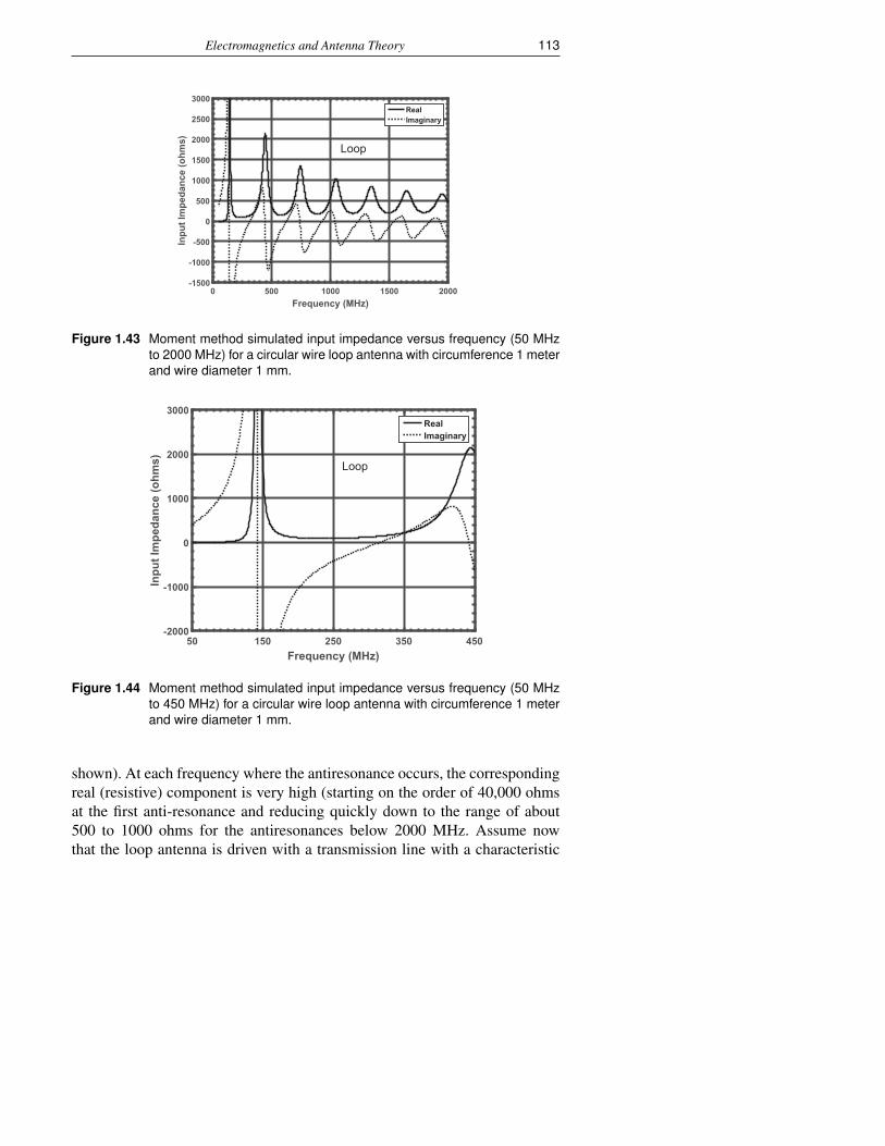
Electromagnetics and Antenna Theory 113
0 500 1000 1500 2000Frequency (MHz)
-1500
-1000
-500
0
500
1000
1500
2000
2500
3000
Inpu
t Im
peda
nce
(ohm
s)
RealImaginary
Loop
Figure 1.43 Moment method simulated input impedance versus frequency (50 MHzto 2000 MHz) for a circular wire loop antenna with circumference 1 meterand wire diameter 1 mm.
50 150 250 350 450Frequency (MHz)
-2000
-1000
0
1000
2000
3000
Inpu
t Im
peda
nce
(ohm
s)
RealImaginary
Loop
Figure 1.44 Moment method simulated input impedance versus frequency (50 MHzto 450 MHz) for a circular wire loop antenna with circumference 1 meterand wire diameter 1 mm.
shown). At each frequency where the antiresonance occurs, the correspondingreal (resistive) component is very high (starting on the order of 40,000 ohmsat the first anti-resonance and reducing quickly down to the range of about500 to 1000 ohms for the antiresonances below 2000 MHz. Assume nowthat the loop antenna is driven with a transmission line with a characteristic
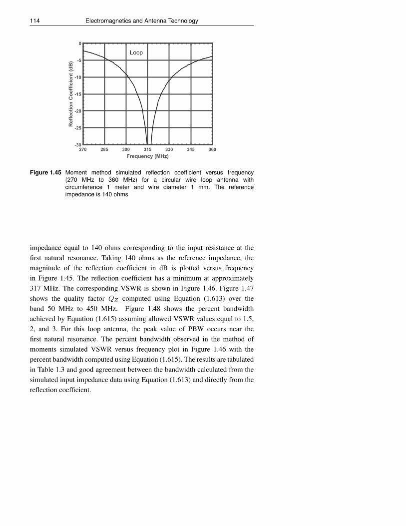
114 Electromagnetics and Antenna Technology
270 285 300 315 330 345 360Frequency (MHz)
-30
-25
-20
-15
-10
-5
0
Ref
lect
ion
Coe
ffici
ent (
dB)
Loop
Figure 1.45 Moment method simulated reflection coefficient versus frequency(270 MHz to 360 MHz) for a circular wire loop antenna withcircumference 1 meter and wire diameter 1 mm. The referenceimpedance is 140 ohms
impedance equal to 140 ohms corresponding to the input resistance at thefirst natural resonance. Taking 140 ohms as the reference impedance, themagnitude of the reflection coefficient in dB is plotted versus frequencyin Figure 1.45. The reflection coefficient has a minimum at approximately317 MHz. The corresponding VSWR is shown in Figure 1.46. Figure 1.47shows the quality factor QZ computed using Equation (1.613) over theband 50 MHz to 450 MHz. Figure 1.48 shows the percent bandwidthachieved by Equation (1.615) assuming allowed VSWR values equal to 1.5,2, and 3. For this loop antenna, the peak value of PBW occurs near thefirst natural resonance. The percent bandwidth observed in the method ofmoments simulated VSWR versus frequency plot in Figure 1.46 with thepercent bandwidth computed using Equation (1.615). The results are tabulatedin Table 1.3 and good agreement between the bandwidth calculated from thesimulated input impedance data using Equation (1.613) and directly from thereflection coefficient.
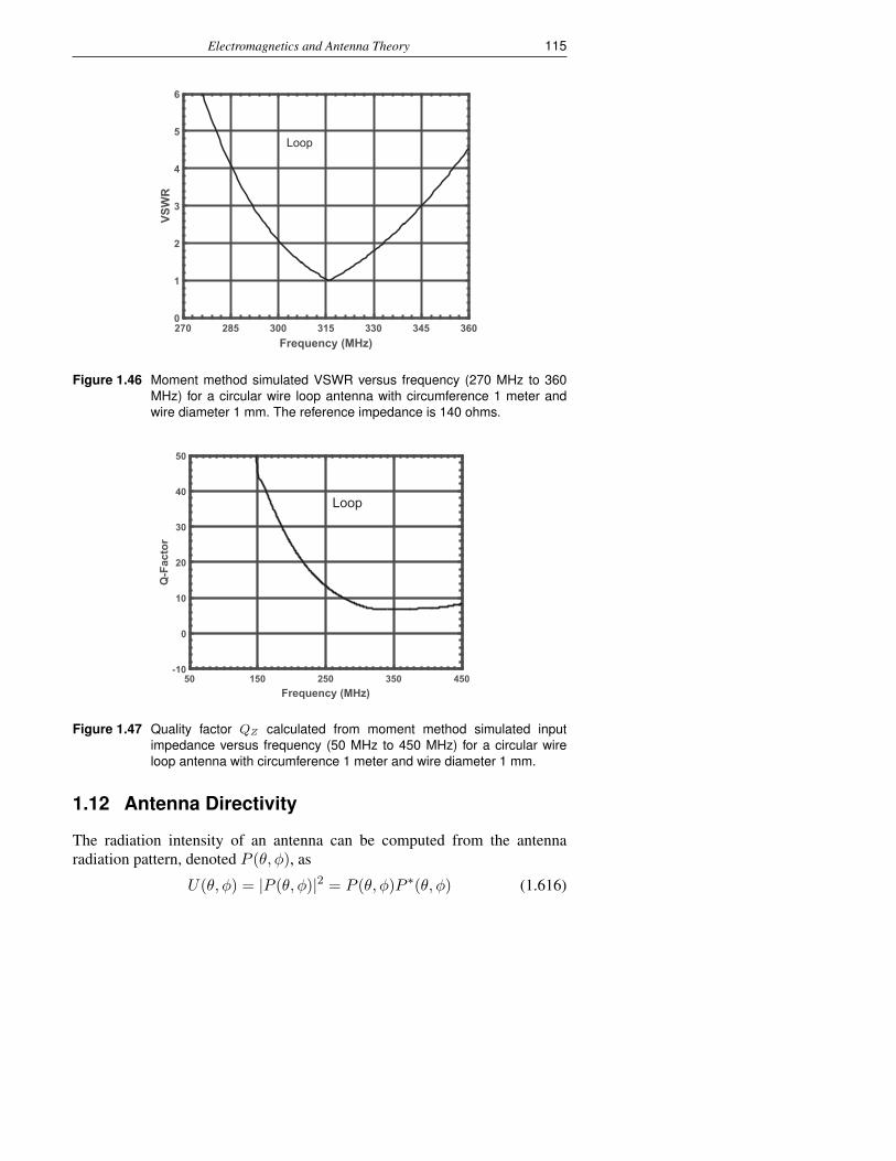
Electromagnetics and Antenna Theory 115
270 285 300 315 330 345 360Frequency (MHz)
0
1
2
3
4
5
6
VSW
R
Loop
Figure 1.46 Moment method simulated VSWR versus frequency (270 MHz to 360MHz) for a circular wire loop antenna with circumference 1 meter andwire diameter 1 mm. The reference impedance is 140 ohms.
50 150 250 350 450Frequency (MHz)
-10
0
10
20
30
40
50
Q-F
acto
r
Loop
Figure 1.47 Quality factor QZ calculated from moment method simulated inputimpedance versus frequency (50 MHz to 450 MHz) for a circular wireloop antenna with circumference 1 meter and wire diameter 1 mm.
1.12 Antenna Directivity
The radiation intensity of an antenna can be computed from the antennaradiation pattern, denoted P (θ, φ), as
U(θ, φ) = |P (θ, φ)|2 = P (θ, φ)P ∗(θ, φ) (1.616)
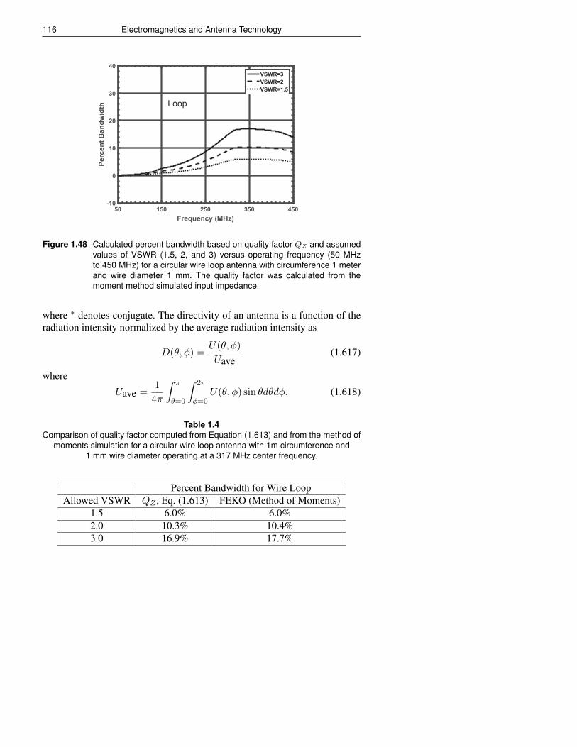
116 Electromagnetics and Antenna Technology
50 150 250 350 450Frequency (MHz)
-10
0
10
20
30
40
Perc
ent B
andw
idth
VSWR=3VSWR=2VSWR=1.5
Loop
Figure 1.48 Calculated percent bandwidth based on quality factor QZ and assumedvalues of VSWR (1.5, 2, and 3) versus operating frequency (50 MHzto 450 MHz) for a circular wire loop antenna with circumference 1 meterand wire diameter 1 mm. The quality factor was calculated from themoment method simulated input impedance.
where ∗ denotes conjugate. The directivity of an antenna is a function of theradiation intensity normalized by the average radiation intensity as
D(θ, φ) =U(θ, φ)
Uave(1.617)
where
Uave =1
4π
∫ π
θ=0
∫ 2π
φ=0U(θ, φ) sin θdθdφ. (1.618)
Table 1.4Comparison of quality factor computed from Equation (1.613) and from the method of
moments simulation for a circular wire loop antenna with 1m circumference and1 mm wire diameter operating at a 317 MHz center frequency.
Percent Bandwidth for Wire LoopAllowed VSWR QZ , Eq. (1.613) FEKO (Method of Moments)
1.5 6.0% 6.0%2.0 10.3% 10.4%3.0 16.9% 17.7%

Electromagnetics and Antenna Theory 117
The antenna directivity,D(θ, φ), relative to an isotropic radiator, depends onlyon the shape of the radiation pattern of the antenna and does not depend onpower delivered to the antenna. The antenna directivity in decibels relative toan isotropic radiator (dBi) is computed by evaluating 10 log10D(θ, φ).
1.12.1 Hertzian Dipole or Electrically Small Loop DirectivityPattern
Consider now the far-field radiation pattern of a z-directed Hertzian (elec-trically short) dipole antenna (refer to Figure 1.25), which has a θ electricfield component that varies in observation angle only as sin θ accordingto Equation (1.488). Now for the Hertzian dipole, since U(θ) = | sin θ|2,it follows from Equation (1.618) that Uave = 2
3 . Substituting this value ofaverage radiation intensity into Equation (1.617), it follows that the angulardependence of the Hertzian dipole directivity is expressed as
D(θ) =3
2| sin θ|2 (1.619)
The electrically-short dipole normalized 3D radiation pattern in decibels isshown in Figure 1.49, and it is observed that the pattern is a figure ofrevolution about the z axis, with a null along the z axis. From Equation (1.619)the half-power (−3 dB) beamwidth is 90. A polar diagram of the absolute
Relative Gain (dB) z
xy
Figure 1.49 3D radiation pattern for a z-directed Hertzian dipole in free space.
directivity pattern (θ component) as a function of θ is shown in Figure 1.50,where the peak directivity of 1.76 dBi is observed to occur at θ = 90.An electrically small loop antenna (Figure 1.25) has the same sin θ angular
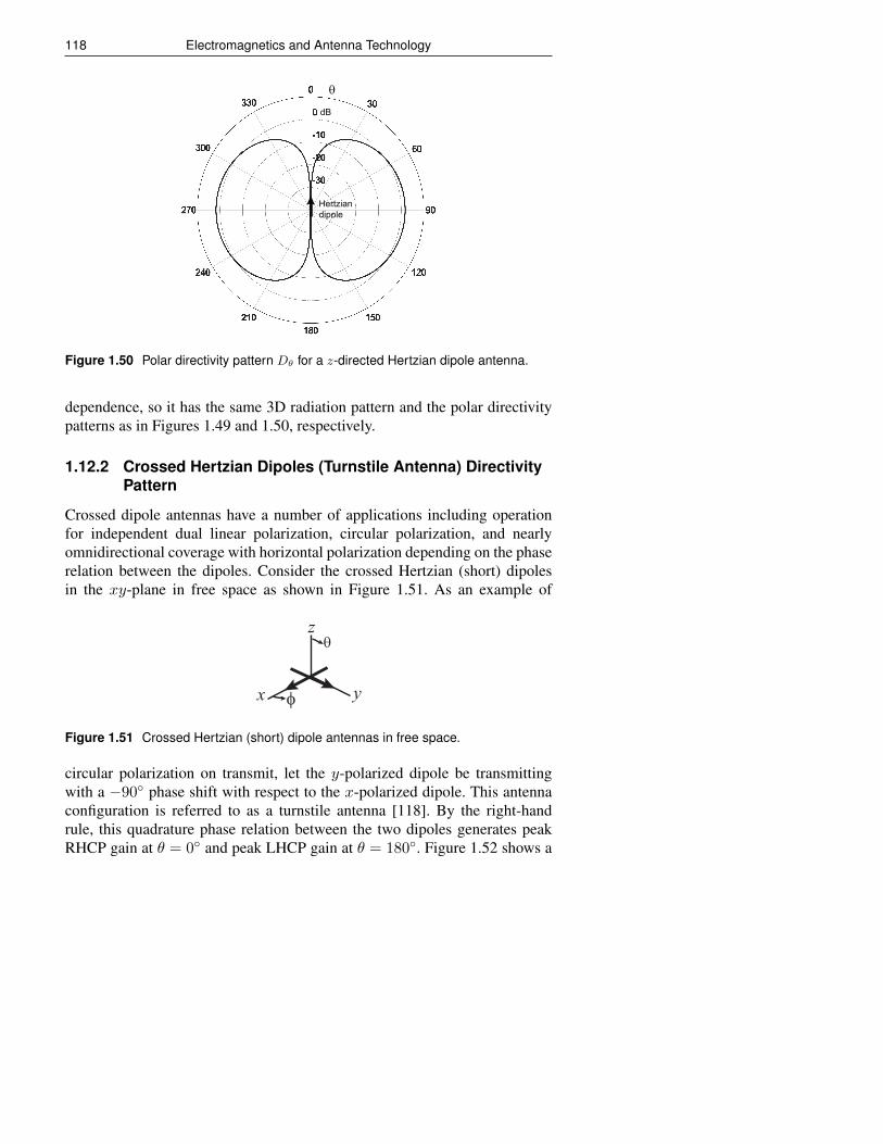
118 Electromagnetics and Antenna Technology
dB
θ
Hertziandipole
Figure 1.50 Polar directivity pattern Dθ for a z-directed Hertzian dipole antenna.
dependence, so it has the same 3D radiation pattern and the polar directivitypatterns as in Figures 1.49 and 1.50, respectively.
1.12.2 Crossed Hertzian Dipoles (Turnstile Antenna) DirectivityPattern
Crossed dipole antennas have a number of applications including operationfor independent dual linear polarization, circular polarization, and nearlyomnidirectional coverage with horizontal polarization depending on the phaserelation between the dipoles. Consider the crossed Hertzian (short) dipolesin the xy-plane in free space as shown in Figure 1.51. As an example of
x
z
yφ
θ
Figure 1.51 Crossed Hertzian (short) dipole antennas in free space.
circular polarization on transmit, let the y-polarized dipole be transmittingwith a −90 phase shift with respect to the x-polarized dipole. This antennaconfiguration is referred to as a turnstile antenna [118]. By the right-handrule, this quadrature phase relation between the two dipoles generates peakRHCP gain at θ = 0 and peak LHCP gain at θ = 180. Figure 1.52 shows a
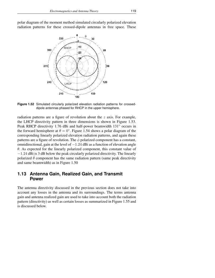
Electromagnetics and Antenna Theory 119
polar diagram of the moment method simulated circularly polarized elevationradiation patterns for these crossed-dipole antennas in free space. These
θ
RHCP
LHCP
Figure 1.52 Simulated circularly polarized elevation radiation patterns for crossed-dipole antennas phased for RHCP in the upper hemisphere.
radiation patterns are a figure of revolution about the z axis. For example,the LHCP directivity pattern in three dimensions is shown in Figure 1.53.Peak RHCP directivity 1.76 dBi and half-power beamwidth 131 occurs inthe forward hemisphere at θ = 0. Figure 1.54 shows a polar diagram of thecorresponding linearly polarized elevation radiation patterns, and again thesepatterns are a figure of revolution. The φ polarized component has a constant,omnidirectional, gain at the level of−1.24 dBi as a function of elevation angleθ. As expected for the linearly polarized component, this constant value of−1.24 dBi is 3 dB below the peak circularly polarized directivity. The linearlypolarized θ component has the same radiation pattern (same peak directivityand same beamwidth) as in Figure 1.50
1.13 Antenna Gain, Realized Gain, and TransmitPower
The antenna directivity discussed in the previous section does not take intoaccount any losses in the antenna and its surroundings. The terms antennagain and antenna realized gain are used to take into account both the radiationpattern (directivity) as well as certain losses as summarized in Figure 1.55 andis discussed below.
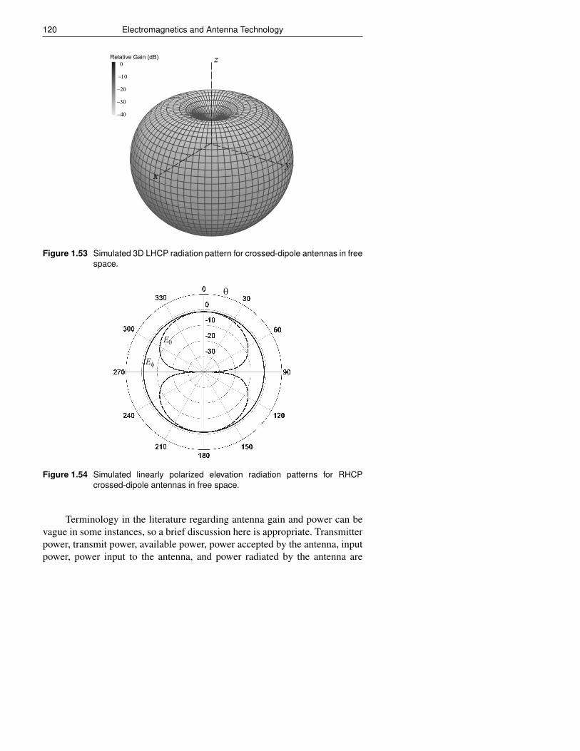
120 Electromagnetics and Antenna Technology
Relative Gain (dB)
−40
−20
0
−10
−30
x
z
y
Figure 1.53 Simulated 3D LHCP radiation pattern for crossed-dipole antennas in freespace.
Eφ
Eθ
θ
Figure 1.54 Simulated linearly polarized elevation radiation patterns for RHCPcrossed-dipole antennas in free space.
Terminology in the literature regarding antenna gain and power can bevague in some instances, so a brief discussion here is appropriate. Transmitterpower, transmit power, available power, power accepted by the antenna, inputpower, power input to the antenna, and power radiated by the antenna are
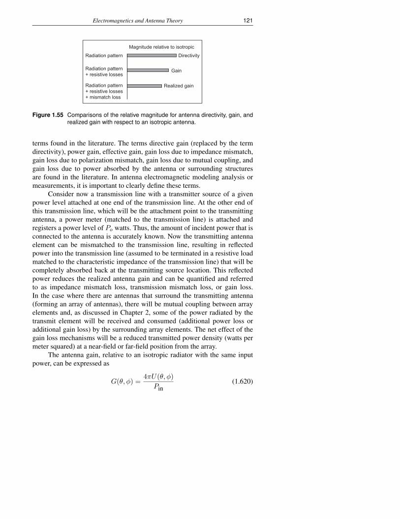
Electromagnetics and Antenna Theory 121
Radiation pattern
Radiation pattern+ resistive losses
Radiation pattern+ resistive losses+ mismatch loss
Magnitude relative to isotropic
Directivity
Gain
Realized gain
Figure 1.55 Comparisons of the relative magnitude for antenna directivity, gain, andrealized gain with respect to an isotropic antenna.
terms found in the literature. The terms directive gain (replaced by the termdirectivity), power gain, effective gain, gain loss due to impedance mismatch,gain loss due to polarization mismatch, gain loss due to mutual coupling, andgain loss due to power absorbed by the antenna or surrounding structuresare found in the literature. In antenna electromagnetic modeling analysis ormeasurements, it is important to clearly define these terms.
Consider now a transmission line with a transmitter source of a givenpower level attached at one end of the transmission line. At the other end ofthis transmission line, which will be the attachment point to the transmittingantenna, a power meter (matched to the transmission line) is attached andregisters a power level of Po watts. Thus, the amount of incident power that isconnected to the antenna is accurately known. Now the transmitting antennaelement can be mismatched to the transmission line, resulting in reflectedpower into the transmission line (assumed to be terminated in a resistive loadmatched to the characteristic impedance of the transmission line) that will becompletely absorbed back at the transmitting source location. This reflectedpower reduces the realized antenna gain and can be quantified and referredto as impedance mismatch loss, transmission mismatch loss, or gain loss.In the case where there are antennas that surround the transmitting antenna(forming an array of antennas), there will be mutual coupling between arrayelements and, as discussed in Chapter 2, some of the power radiated by thetransmit element will be received and consumed (additional power loss oradditional gain loss) by the surrounding array elements. The net effect of thegain loss mechanisms will be a reduced transmitted power density (watts permeter squared) at a near-field or far-field position from the array.
The antenna gain, relative to an isotropic radiator with the same inputpower, can be expressed as
G(θ, φ) =4πU(θ, φ)
Pin(1.620)
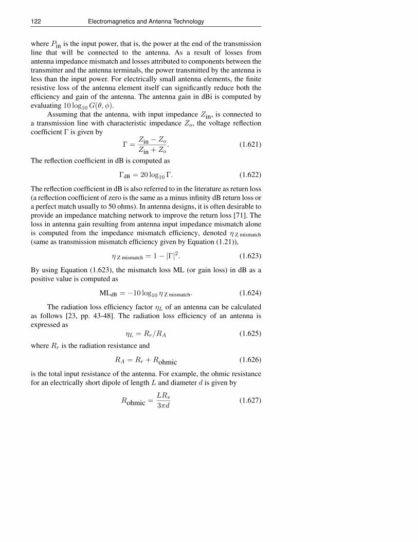
122 Electromagnetics and Antenna Technology
where Pin is the input power, that is, the power at the end of the transmissionline that will be connected to the antenna. As a result of losses fromantenna impedance mismatch and losses attributed to components between thetransmitter and the antenna terminals, the power transmitted by the antenna isless than the input power. For electrically small antenna elements, the finiteresistive loss of the antenna element itself can significantly reduce both theefficiency and gain of the antenna. The antenna gain in dBi is computed byevaluating 10 log10G(θ, φ).
Assuming that the antenna, with input impedance Zin, is connected toa transmission line with characteristic impedance Zo, the voltage reflectioncoefficient Γ is given by
Γ =Zin − ZoZin + Zo
. (1.621)
The reflection coefficient in dB is computed as
ΓdB = 20 log10 Γ. (1.622)
The reflection coefficient in dB is also referred to in the literature as return loss(a reflection coefficient of zero is the same as a minus infinity dB return loss ora perfect match usually to 50 ohms). In antenna designs, it is often desirable toprovide an impedance matching network to improve the return loss [71]. Theloss in antenna gain resulting from antenna input impedance mismatch aloneis computed from the impedance mismatch efficiency, denoted η Z mismatch(same as transmission mismatch efficiency given by Equation (1.21)),
η Z mismatch = 1− |Γ|2. (1.623)
By using Equation (1.623), the mismatch loss ML (or gain loss) in dB as apositive value is computed as
MLdB = −10 log10 η Z mismatch. (1.624)
The radiation loss efficiency factor ηL of an antenna can be calculatedas follows [23, pp. 43-48]. The radiation loss efficiency of an antenna isexpressed as
ηL = Rr/RA (1.625)
where Rr is the radiation resistance and
RA = Rr +Rohmic (1.626)
is the total input resistance of the antenna. For example, the ohmic resistancefor an electrically short dipole of length L and diameter d is given by
Rohmic =LRs3πd
(1.627)

Electromagnetics and Antenna Theory 123
whereRs =
√πfµ/σ (1.628)
is the surface resistance of the dipole, which depends on the frequency f ,permeability µ, and electrical conductivity σ of the dipole material. Thus,since the ohmic resistance is inversely proportional to the dipole diameter, theefficiency can be increased by using a larger-diameter dipole.
The realized antenna gain, denoted as Grealized, takes account ofimpedance mismatch and efficiency loss. The realized antenna gain anddirectivity are related by the following expression
Grealized(θ, φ) = D(θ, φ)ηLη Z mismatch (1.629)
where ηL is the antenna efficiency loss factor, which includes resistive lossesin the antenna. For a 100% efficient (lossless) antenna with ηL = 1, and withno mismatch loss, the gain is equal to the directivity. For a transmittingantenna, the effective isotropic radiated power (EIRP(θ, φ)) is equal to theproduct of the power incident on the antenna Po and the realized gainGrealized(θ, φ), that is
EIRP(θ, φ) = PoGrealized(θ, φ). (1.630)
Alternately, if the impedance mismatch loss is included in the power budget,then the transmit power accepted by the antenna is denoted as Pt and then theEIRP is equal to the following product
EIRP(θ, φ) = PtGt(θ, φ) (1.631)
where Gt(θ, φ) is the gain of the transmit antenna, which includes anyresistive losses associated with the antenna and its surroundings.
The far-zone power density Pd (with units of W/m2) at a distance r fromthe aperture (one-way path) is given by
Pd =PtGt4πr2
. (1.632)
Based on a receive antenna’s maximum effective aperture, denoted Aem, theaperture collects incident power density and converts it to an output power.Thus, the received power Pr of an antenna aperture can be expressed as
Pr = PdAem. (1.633)
Furthermore, the receive antenna gain is expressed as
Gr = 4πAem/λ2, (1.634)

124 Electromagnetics and Antenna Technology
and solving for Aem yields
Aem = Grλ2/(4π). (1.635)
Thus, it follows that
Pr =PtGtGrλ
2
(4πr)2. (1.636)
Equation (1.636) can be rearranged to express the mutual coupling power ratio(Pr/Pt) between two antennas as
PrPt
=GtGrλ
2
(4πr)2. (1.637)
1.14 Summary
The theory given in this chapter can be used to gain some basic insight intothe fundamental radiation properties of antennas. In the case of an array ofantennas, the radiation properties of one array antenna element have an effecton the surrounding array antenna elements, and thus the interaction betweenthe array antenna elements must be taken into account in any detailed analysis.Some methods for computing the performance of phased array antennastaking account of mutual coupling effects are discussed in Chapter 2.

Electromagnetics and Antenna Theory 125
References[1] T.K. Sarkar, R.J. Mailloux, A.A. Oliner, M. Salazar-Palma, D.L. Sengupta, History of
Wireless, Hoboken, NJ: Wiley, 2006.
[2] C.A. Balanis, Advanced Engineering Electromagnetics, 2nd ed. New Jersey: Wiley,2012.
[3] J.A. Kong, Electromagnetic Wave Theory. Cambridge, Mass.: EMW Publishing, 2008.
[4] D.T. Paris and F.K. Hurd, Basic Electromagnetic Theory. New York: McGraw-Hill,1969.
[5] J.A. Stratton, Electromagnetic Theory. New York: McGraw-Hill, 1941.
[6] J.D. Kraus, Electromagnetics. New York: McGraw-Hill, 1953.
[7] R.F. Harrington, Time-Harmonic Electromagnetic Fields. New York: McGraw-Hill,1961.
[8] W.H. Hayt and J.A. Buck, Engineering Electromagnetics, 6th ed. New York: McGraw-Hill, 2001.
[9] C.H. Durney and C.C. Johnson, Introduction to Modern Electromagnetics. New York:McGraw-Hill, 1969.
[10] J.D. Kraus and K.R. Carver, Electromagnetics, 2nd ed. New York: McGraw-Hill, 1973,pp. 612–613.
[11] D.K. Cheng, Field and Wave Electromagnetics. Reading, Mass.: Addison-Wesley, 1983.
[12] S. Ramo, J.R. Whinnery, and T. van Duzer, Fields and Waves in CommunicationElectronics. New York: Wiley, 1984.
[13] M.N.O. Sadiku, Elements of Electromagnetics, 2nd ed. New York: Oxford UniversityPress, 1995.
[14] G.S. Smith, An Introduction to Classical Electromagnetic Radiation. Cambridge, UK:Cambridge University Press, 1997.
[15] J.D. Kraus and R.J. Marhefka, Antennas for All Applications, 3rd ed. New York:McGraw-Hill, 2002.
[16] R.W.P. King, The Theory of Linear Antennas, Cambridge, MA: Harvard UniversityPress, 1956.
[17] S.A. Schelkunoff and H.T. Friis, Antennas: Theory and Practice. New York: Wiley,1952.
[18] S. Silver, ed., Microwave Antenna Theory and Design, MIT Radiation Lab Series, vol.12, New York: McGraw-Hill, 1949.
[19] C.H. Walter, Traveling Wave Antennas, New York: McGraw-Hill, 1968.
[20] W.L. Weeks, Antenna Engineering, New York: McGraw-Hill, 1968.
[21] R.S. Elliott, Antenna Theory and Design, New York: Prentice-Hall, 1981.

126 Electromagnetics and Antenna Technology
[22] A.W. Rudge, K. Milne, A.D. Olver, and P. Knight, The Handbook of Antenna Design,vols. 1 and 2 London: Peter Perigrinus, 1992.
[23] W.L. Stutzman and G.A. Thiele, Antenna Theory and Design, 2nd ed. New York: Wiley,1998.
[24] J. Volakis, ed., Antenna Engineering Handbook, 4th ed. New York: McGraw-Hill, 2007.
[25] C.A. Balanis, Antenna Theory and Design, 3rd ed. New York: Wiley, 2005.
[26] R.A. Burberry, VHF and UHF Antennas London: Peter Peregrinus, 1992.
[27] T.A. Milligan, Modern Antenna Design, 2nd ed. Hoboken, NJ: Wiley-IEEE Press, 2005
[28] L.V. Blake and M.W. Long, Antennas: Fundamentals, Design, Measurement, Raleigh,NC: SciTech Publishing, 2009.
[29] W. Stutzman, “Bibliography for Antennas: A List of Every English-Language AntennaBook Ever Written," IEEE Antennas and Propagation Magazine, vol. 50, no. 4, August2008, pp. 128–143.
[30] N. Amitay, V. Galindo, and C.P. Wu, Theory and Analysis of Phased Array Antennas.New York: Wiley, 1972, ch. 1.
[31] A.A. Oliner and G.H. Knittel, eds., Phased Array Antennas. Dedham, Mass.: ArtechHouse, 1972.
[32] R.C. Hansen, ed., Significant Phased Array Papers. Dedham, Mass.: Artech House,1973.
[33] R.J. Mailloux, Phased Array Handbook, 2nd ed. Norwood, Mass.: Artech House, 2005.
[34] E. Brookner, ed., Practical Phased-Array Antenna Systems. Norwood, Mass.: ArtechHouse, 1991.
[35] R.C. Hansen, Microwave Scanning Antennas, vol. II: Array Theory and Practice. LosAltos, Calif.: Peninsula Publishing, 1985.
[36] R.C. Hansen, Phased Array Antennas, 2nd ed. New York: Wiley, 2009.
[37] A.K. Bhattacharyya, Phased Array Antennas. New York: Wiley, 2006.
[38] T. Jeffrey, Phased-Array Radar Design: Application of Radar Fundamentals. Raleigh,North Carolina: Scitech Pub Inc., 2009.
[39] A.J. Fenn, Adaptive Antennas and Phased Arrays for Radar and Communications.Norwood, Mass.: Artech House, 2008.
[40] S.P. Skobelev, Phased Array Antennas with Optimized Element Patterns. Norwood,Mass.: Artech House, 2011.
[41] H.J. Visser, Array and Phased Array Antenna Basics. New York: Wiley, 2005.
[42] R.L. Haupt, Antenna Arrays: A Computational Approach. New York: Wiley-IEEE Press,2010.

Electromagnetics and Antenna Theory 127
[43] D. Ehyale, Novel Approaches to the Design of Phased Array Antennas: Low Cost, LowComplexity Phased Array Antenna Design. LAP Lambert Academic Publishing, 2012.
[44] E. Brookner, “Phased-Array Radars,” Scientific American, vol. 252, no. 2, 1985, pp. 94–102.
[45] A.J. Fenn, D.H. Temme, W.P. Delaney, and W.E. Courtney, “The Development ofPhased Array Radar Technology,” Lincoln Laboratory Journal, vol. 12, no. 2, 2000,pp. 321–340.
[46] R.J. Mailloux, “Phased Array Theory and Technology,” Proc. IEEE, vol. 70, no. 3, 1982,pp. 246–291.
[47] A.J. Fenn and P.T. Hurst, Ultrawideband Phased Array Antenna Technology for Sensingand Communications Systems, Cambridge, MA: The MIT Press, 2015.
[48] P.W. Howells, “Explorations in Fixed and Adaptive Resolution at GE and SURC,” IEEETrans. Antennas and Propagation, vol. 24, no. 5, 1976, pp. 575–584.
[49] S.P. Applebaum, “Adaptive Arrays,” IEEE Trans. Antennas and Propagation, vol. 24,no. 5, 1976, pp. 585–598.
[50] W.F. Gabriel, “Adaptive Arrays – An Introduction,” Proc. IEEE, vol. 64, 1976, pp. 239–271.
[51] J.T. Mayhan, “Some Techniques for Evaluating the Bandwidth Characteristics ofAdaptive Nulling Systems,” IEEE Trans. Antennas and Propagation, vol. 27, no. 3,1979, pp. 363–373.
[52] J.T. Mayhan, A.J. Simmons, and W.C. Cummings, “Wide-Band Adaptive AntennaNulling Using Tapped Delay Lines,” IEEE Trans. Antennas and Propagation, vol. 29,no. 6, 1981, pp. 923–936.
[53] A.J. Fenn, “Evaluation of Adaptive Phased Array Far-Field Nulling Performance in theNear-Field Region,” IEEE Trans. Antennas and Propagation, vol. 38, no. 2, 1990, pp.173–185.
[54] R.A. Monzingo and T.W. Miller, Introduction to Adaptive Arrays. New York: Wiley,1980.
[55] R.T. Compton, Jr., Adaptive Antennas, Concepts and Performance. Upper Saddle River,New Jersey: Prentice-Hall, 1988.
[56] M.M. Weiner, Adaptive Antennas and Receivers. Boca Raton, Florida: CRC Press, 2006.
[57] S. Chandran, ed., Adaptive Antenna Arrays: Trends and Applications. Berlin: Springer-Verlag, 2004.
[58] D.G. Manolakis, V.K. Ingle, and S.M. Kogon, Statistical and Adaptive SignalProcessing: Spectral Estimation, Signal Modeling, Adaptive Filtering, and ArrayProcessing. Norwood, Mass.: Artech House, 2005.
[59] R. Nitzberg, Adaptive Signal Processing for Radar. Norwood, Mass.: Artech House,1992.
[60] A. Farina, Antenna-Based Signal Processing Techniques for Radar Systems. Norwood,

128 Electromagnetics and Antenna Technology
Mass.: Artech House, 1992.
[61] J.E. Hudson, Adaptive Array Principles. New York: Peter Peregrinus, 1981.
[62] D.M. Pozar, Microwave Engineering, 4th ed., Hoboken, NJ: Wiley, 2012.
[63] P. H. Smith, “Transmission line calculator,” Electronics, vol. 12, no. 1, pp. 29–31, Jan.1939.
[64] P. H. Smith, “An Improved Transmission Line Calculator,” Electronics, vol. 17, no. 1,pp. 130–133, p. 318, p. 320, p. 322, and pp. 324–325, Jan. 1944.
[65] P. H. Smith, “Electronic Applications of the Smith Chart,” – In Waveguide, Circuit, andComponent Analysis, 2nd ed. Raleigh, NC: SciTech Publishing, 1995.
[66] T. Lee, “The Smith Chart Comes Home,” IEEE Microwave Magazine, p. 10, 12,and 25, Nov. 2015, Digital Object Identifier: 10.1109/MMM.2015.2467953, Date ofPublication: 14 Oct. 2015.
[67] H.J. Reich, ed., Harvard Radio Research Laboratories, Very High Frequency Techniques,New York: Mc-Graw Hill, Vol. 1, Chapter 3, 1947.
[68] R.M. Fano, “Theoretical Limitations on the Broadband Matching of ArbitraryImpedances,” Massachusetts Institute of Technology, Research Laboratory ofElectronics, Technical Report 41, Jan. 2, 1948.
[69] H.A. Wheeler, “Wideband Impedance Matching,” Wheeler Laboratories Report 418,Great Neck, New York, 1950.
[70] V.H. Rumsey, “The Design of Frequency-Compensating Matching Sections,” Proc. IRE,October 1950, pp. 1191–1196.
[71] R.L. Thomas, A Practical Introduction to Impedance Matching, Dedham, MA: ArtechHouse, 1976.
[72] W.N. Caron, Antenna Impedance Matching, Newington, CT: American Radio RelayLeague, 1989.]
[73] G.L. Matthaei, L. Young, E.M.T. Jones, Microwave Filters, Impedance-MatchingNetworks, and Coupling Structures, New York, McGraw-Hill, 1964.
[74] T.R. Cuthbert, Circuit Design Using Personal Computers, New York: John Wiley, 1983.
[75] T.R. Cuthbert, Broadband Direct-Coupled and Matching RF Networks, Greenwood,Arkansas: TRCPEP Publications, 1999.
[76] C. Bowick, RF Circuit Design, Burlington, MA: Newnes, 2008.
[77] R. Mavaddat, Network Scattering Parameters, Advanced Series in Circuits and Systems,vol. 2, Singapore, World Scientific Publishing, 1996.
[78] D.A. Frickey, “Conversions Between S, Z, Y, h, ABCD, and T Parameters Which areValid for Complex Source and Load Impedances,” IEEE Trans. Microwave Theory andTechniques, vol. 42, no. 2, February 1994, pp. 205-211.
[79] W.F. Egan, Practical RF System Design, New York: IEEE, Hoboken, New Jersey: Wiley.

Electromagnetics and Antenna Theory 129
[80] IEEE Standard for Ultrawideband Radar Definitions, IEEE Std 1672-2006, 4 May 2007(2nd printing, 11 Dec. 2008), doi: 10.1109/IEEESTD.2007.359972.
[81] J.D. Taylor, Introduction to Ultra-Wideband Radar Systems. Boca Raton, Florida: CRCPress, 1995.
[82] L. Peters, Jr., J.J. Daniels, and J.D. Young, “Ground Penetrating Radar as a SubsurfaceEnvironmental Sensing Tool," Proc. IEEE, vol. 82, no. 12, 1994, pp. 1802–1822.
[83] D. Uduwawala et al., “A Deep Parametric Study of Resistor-Loaded Bow-Tie Antennasfor Ground-Penetrating Radar Applications Using FDTD," IEEE Trans Geoscience andRemote Sensing, vol. 42, no. 4, 2004, pp. 732–742.
[84] M. Kanda, “A Relatively Short Cylindrical Broadband Antenna with Tapered ResistiveLoading for Picosecond Pulse Measurements," IEEE Trans. Antennas and Propagation,vol. 26, no. 3, 1978, pp. 439–447.
[85] T.P. Montoya and G.S. Smith, “Land Mine Detection Using a Ground Penetrating RadarBased on Resistively Loaded Vee Dipoles," IEEE Trans. Antennas and Propagation,vol. 47, no. 12, 1999, pp. 1795–1806.
[86] J.D. Dyson, “The Equiangular Spiral Antenna," IRE Trans. Antennas and Propagation,vol. 7, no. 2, 1959, pp. 181–187.
[87] V.H. Rumsey, Frequency Independent Antennas. New York: Academic Press, Inc., 1966.
[88] H. Schantz, The Art and Science of Ultrawideband Antennas. Norwood, Mass.: ArtechHouse, 2005.
[89] D. Valderas, J.I. Sancho, D. Puente, C. Ling, and X. Chen, Ultrawideband Antennas,Design and Applications. London: Imperial College Press, 2011.
[90] T.S. Ralston, G.L. Charvat, and J.E. Peabody, “Real-Time Through-Wall ImagingUsing an Ultrawideband Multiple-Input Multiple-Output (MIMO) Phased Array RadarSystem," IEEE Int. Symp. on Phased Array Systems and Technology, 2010, pp. 551–558.
[91] A. Rajagopalan, G. Gupta, A.S. Konanur, B. Hughes, and G. Lazzi, “Increasing ChannelCapacity of an Ultrawideband MIMO System Using Vector Antennas," IEEE Trans. onAntennas and Propagation, vol. 55, no. 10, 2007, pp. 2880–2887.
[92] C.M. Keller, and D.P. Young, “Ultra-Wideband (UWB) Signal Localization Using aVehicle-Sized Array," 2005 IEEE International Conference on Ultra-Wideband, 2005,pp. 290–295.
[93] E.W. Reid, L. Ortiz-Balbuena, A. Ghadiri, and K. Moez, “A 324-Element VivaldiAntenna Array for Radio Astronomy Instrumentation," IEEE Trans. Instrumentationand Measurement, vol. 61, no. 1, 2012, pp. 241–250.
[94] M. Lazebnik, E.L. Madsen, G.R. Frank, and S.C. Hagness, “Tissue-Mimicking PhantomMaterials for Narrowband and Ultrawideband Microwave Applications,” Physics inMedicine and Biology, vol. 50, 2005, pp. 4245–4258.
[95] S. Gabriel, R.W. Lau, and C. Gabriel, “The Dielectric Properties of Biological Tissues:

130 Electromagnetics and Antenna Technology
Part III. Parametric Models for the Dielectric Spectrum of Tissues,” Physics in Medicineand Biology, vol. 41, 1996, pp. 2271–2293, online http://niremf.ifac.cnr.it/tissprop.
[96] C-K Chou and J. D’Andrea, IEEE Standard for Safety Levels with Respect to HumanExposure to Radio Frequency Electromagnetic Fields, 3 kHz to 300 GHz, IEEE StdC95.1-2005. New York: Institute of Electrical and Electronics Engineers, Inc.
[97] J.F. Lehmann, ed., Therapeutic Heat and Cold, 3rd ed. Baltimore, Maryland: Williams& Wilkins, 1982.
[98] A.R. von Hippel, Dielectrics and Waves. New York: John Wiley, 1954.
[99] A.D. Yaghjian and S.R. Best, Impedance, Bandwidth, and Q of Antennas, IEEE Trans.Antennas and Propagat., vol. 53, no. 4, April 2005, pp. 1298–1324.
[100] C. Cohen-Tannoudji, J. Dupont-Roc, and G. Grynberg, Photons and Atoms:Introduction to Quantum Electrodynamics. Weinheim: Wiley-VCH, Verlag GmbH &Co. KGaA, 2004.
[101] C. Cohen-Tannoudji, J. Dupont-Roc, and G. Grynberg, Atom-Photon Interactions:Basic Processes and Applications. Weinheim: Wiley-VCH, Verlag GmbH & Co. KGaA,2004.
[102] J.D. Jackson, Classical Electrodynamics, 3rd ed. New York: Wiley, 1999, p. 3.
[103] J.C. Maxwell, A Treatise on Electricity and Magnetism, vols. 1 and 2. Oxford, UK:Clarendon Press, 1873.
[104] J.H. Poynting, “On the Transfer of Energy in the Electromagnetic Field,” PhilosophicalTransactions of the Royal Society of London, vol. 175, 1884, pp. 343–361.
[105] Y. Zhu and A. Cangellaris, Multigrid Finite Element Methods for Electromagnetic FieldModeling. New Jersey: Wiley, 2006.
[106] W.L. Stutzman, Polarization in Electromagnetic Systems. Norwood, Mass.: ArtechHouse, 1993.
[107] R.E. Collin, Foundations for Microwave Engineering. New York: McGraw-Hill, 1966,pp. 64–143.
[108] P.G. Ciarlet, ed., Numerical Methods in Electromagnetics, Volume 13: Special Volume(Handbook of Numerical Analysis). W.H.A. Schilders and E.J.W. ter Maten, guest eds.,Chapter 3, Finite Difference Time Domain Methods, S.C. Hagness, A. Taflove, and S.D.Gedney, Elsevier B.V., The Netherlands, 2005, pp. 199–314.
[109] C.T. Tai, Dyadic Green’s Functions in Electromagnetic Theory. London: IntextEducational Publishers, 1971.
[110] C.T. Tai, Generalized Vector and Dyadic Analysis. New York: IEEE Press, 1992.
[111] C.T. Tai, “A Survey of the Improper Uses of ∇ in Vector Analysis," RadiationLaboratory, The University of Michigan, Technical Report RL 909, November 1994.
[112] C.T. Tai, “A Historical Study of Vector Analysis," Radiation Laboratory, The Universityof Michigan, Technical Report RL 915, May 1995.

Electromagnetics and Antenna Theory 131
[113] G. Green, “An Essay on the Application of Mathematical Analysis to the Theoriesof Electricity and Magnetism," Nottingham, England, printed for the author by T.Wheelhouse, 1828.
[114] D.A. Sanchez-Hernandez, ed., High Frequency Electromagnetic Dosimetry, Norwood,MA: Artech House, 2008.
[115] G.W. Hanson and A.B. Yakovlev, Operator Theory for Electromagnetics, AnIntroduction. New York: Springer, 2002.
[116] R. Nevels and J. Jeong, “The Time Domain Green’s Function and Propagator forMaxwell’s equations," IEEE Trans. Antennas and Propagat., vol. 52, no. 11, 2004, pp.3012–3018.
[117] A.Z. Elsherbeni, P. Nayeri, and C.J. Reddy, Antenna Analysis and Design Using FEKOElectromagnetic Simulation Software, SciTech Publishing, 2014.
[118] G. Brown, “The Turnstile Antenna," Electronics, 1936.

2Phased Array Antennas
2.1 Introduction
In Chapter 1, electromagnetic theory for antennas was reviewed in detail. Inthis chapter, the subject of phased array antennas [1–60] is briefly reviewed.Development of phased array radar technology is described by Fenn et al.[24]. The concept of a phased array and early experiments were presentedover 100 years ago in a 1909 Nobel Prize lecture by Braun [54]. A history ofphased arrays has been reviewed by Mailloux [55]. Delaney [56] has reviewedthe development and deployment of operational phased array radars, with anemphasis on achieving a goal of a solid state phased array. Solid-state phasedarrays are now being utilized in many applications as described by Brookner[57]. Herd and Conway [58] have described the evolution of low-cost solid-state phased arrays that utilize high-volume commercial manufacturing andpackaging technologies that implement a modern tile array architecture.Millimeter-wave phased arrays have been mass produced for automotive radarsystems for collision avoidance [59]. Millimeter-wave phased arrays are beinginvestigated for fifth generation (5G) communications systems for high-data-rate applications [60-62].
This chapter begins with basic phased array theory in Section 2.2. Totake into account the simulated effects of array mutual coupling, equivalenceprinciples (Section 2.3), the reciprocity theorem (Section 2.4) and reactionintegral equation (Section 2.5) are reviewed, from which the method ofmoments (Section 2.6) is derived. The method of moments is used inmany of the electromagnetic simulations of antennas presented in this book.Section 2.7 provides examples of broadside and endfire linear arrays ofHertzian (short) dipoles. An example of mutual coupling effects on theembedded element pattern in a two-dimensional array of linear dipoles is
133
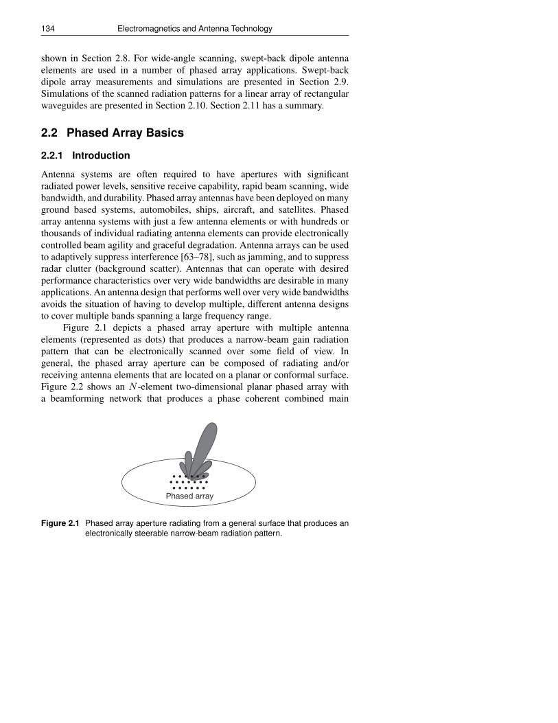
134 Electromagnetics and Antenna Technology
shown in Section 2.8. For wide-angle scanning, swept-back dipole antennaelements are used in a number of phased array applications. Swept-backdipole array measurements and simulations are presented in Section 2.9.Simulations of the scanned radiation patterns for a linear array of rectangularwaveguides are presented in Section 2.10. Section 2.11 has a summary.
2.2 Phased Array Basics
2.2.1 Introduction
Antenna systems are often required to have apertures with significantradiated power levels, sensitive receive capability, rapid beam scanning, widebandwidth, and durability. Phased array antennas have been deployed on manyground based systems, automobiles, ships, aircraft, and satellites. Phasedarray antenna systems with just a few antenna elements or with hundreds orthousands of individual radiating antenna elements can provide electronicallycontrolled beam agility and graceful degradation. Antenna arrays can be usedto adaptively suppress interference [63–78], such as jamming, and to suppressradar clutter (background scatter). Antennas that can operate with desiredperformance characteristics over very wide bandwidths are desirable in manyapplications. An antenna design that performs well over very wide bandwidthsavoids the situation of having to develop multiple, different antenna designsto cover multiple bands spanning a large frequency range.
Figure 2.1 depicts a phased array aperture with multiple antennaelements (represented as dots) that produces a narrow-beam gain radiationpattern that can be electronically scanned over some field of view. Ingeneral, the phased array aperture can be composed of radiating and/orreceiving antenna elements that are located on a planar or conformal surface.Figure 2.2 shows an N -element two-dimensional planar phased array witha beamforming network that produces a phase coherent combined main
Phased array
Figure 2.1 Phased array aperture radiating from a general surface that produces anelectronically steerable narrow-beam radiation pattern.
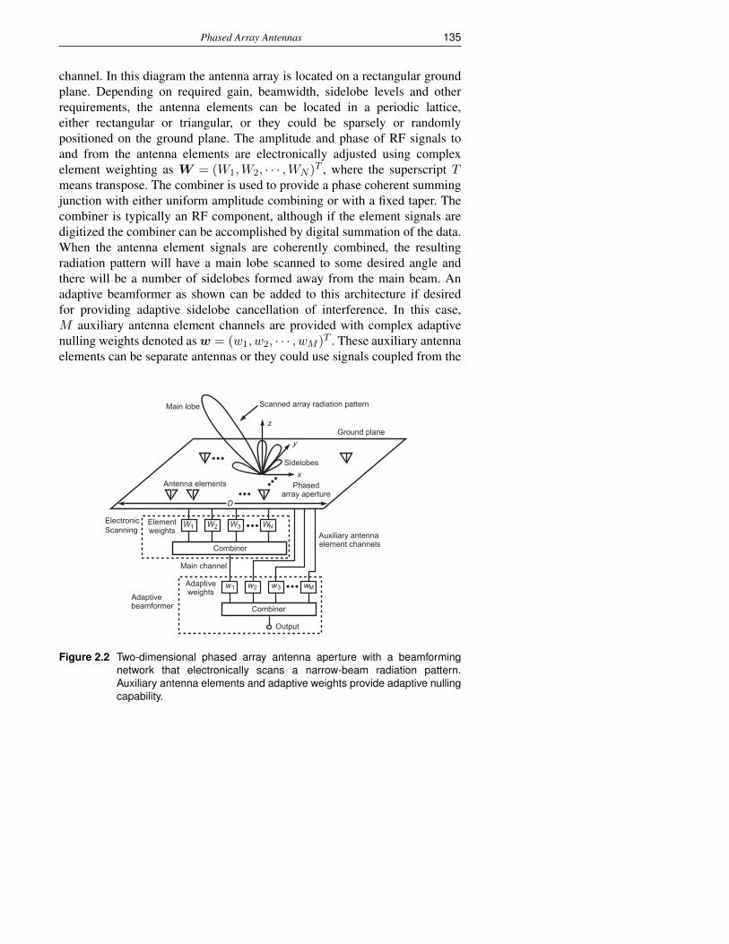
Phased Array Antennas 135
channel. In this diagram the antenna array is located on a rectangular groundplane. Depending on required gain, beamwidth, sidelobe levels and otherrequirements, the antenna elements can be located in a periodic lattice,either rectangular or triangular, or they could be sparsely or randomlypositioned on the ground plane. The amplitude and phase of RF signals toand from the antenna elements are electronically adjusted using complexelement weighting as W = (W1,W2, · · · ,WN )T , where the superscript Tmeans transpose. The combiner is used to provide a phase coherent summingjunction with either uniform amplitude combining or with a fixed taper. Thecombiner is typically an RF component, although if the element signals aredigitized the combiner can be accomplished by digital summation of the data.When the antenna element signals are coherently combined, the resultingradiation pattern will have a main lobe scanned to some desired angle andthere will be a number of sidelobes formed away from the main beam. Anadaptive beamformer as shown can be added to this architecture if desiredfor providing adaptive sidelobe cancellation of interference. In this case,M auxiliary antenna element channels are provided with complex adaptivenulling weights denoted asw = (w1, w2, · · · , wM )T . These auxiliary antennaelements can be separate antennas or they could use signals coupled from the
Output
Auxiliary antenna element channels
Adaptivebeamformer
Main channel
Adaptiveweights
ElectronicScanning
Elementweights
Antenna elements Phasedarray aperture
Sidelobes
D
x
zGround plane
Scanned array radiation patternMain lobe
W1 W2 W3 WN
y
w1 w3 wMw2
Combiner
Combiner
Figure 2.2 Two-dimensional phased array antenna aperture with a beamformingnetwork that electronically scans a narrow-beam radiation pattern.Auxiliary antenna elements and adaptive weights provide adaptive nullingcapability.
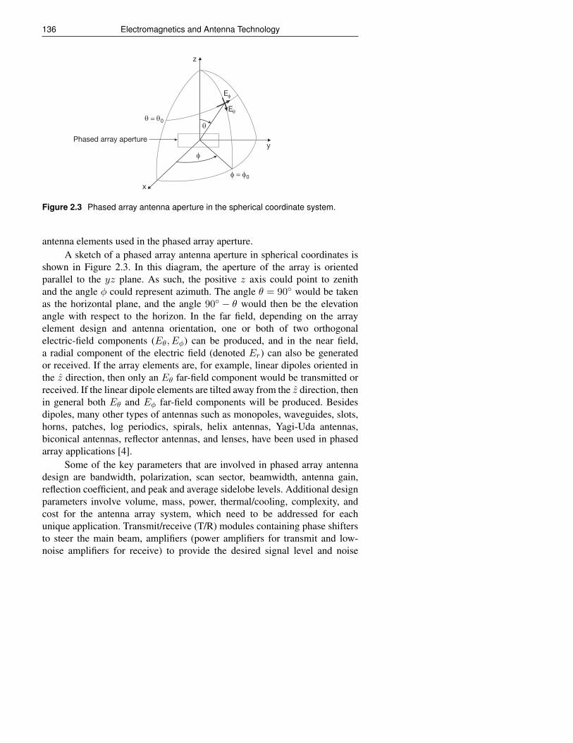
136 Electromagnetics and Antenna Technology
θ = θ0θ
φy
z
x
φ = φ0
Phased array aperture
Eθ
Eφ
Figure 2.3 Phased array antenna aperture in the spherical coordinate system.
antenna elements used in the phased array aperture.A sketch of a phased array antenna aperture in spherical coordinates is
shown in Figure 2.3. In this diagram, the aperture of the array is orientedparallel to the yz plane. As such, the positive z axis could point to zenithand the angle φ could represent azimuth. The angle θ = 90 would be takenas the horizontal plane, and the angle 90 − θ would then be the elevationangle with respect to the horizon. In the far field, depending on the arrayelement design and antenna orientation, one or both of two orthogonalelectric-field components (Eθ, Eφ) can be produced, and in the near field,a radial component of the electric field (denoted Er) can also be generatedor received. If the array elements are, for example, linear dipoles oriented inthe z direction, then only an Eθ far-field component would be transmitted orreceived. If the linear dipole elements are tilted away from the z direction, thenin general both Eθ and Eφ far-field components will be produced. Besidesdipoles, many other types of antennas such as monopoles, waveguides, slots,horns, patches, log periodics, spirals, helix antennas, Yagi-Uda antennas,biconical antennas, reflector antennas, and lenses, have been used in phasedarray applications [4].
Some of the key parameters that are involved in phased array antennadesign are bandwidth, polarization, scan sector, beamwidth, antenna gain,reflection coefficient, and peak and average sidelobe levels. Additional designparameters involve volume, mass, power, thermal/cooling, complexity, andcost for the antenna array system, which need to be addressed for eachunique application. Transmit/receive (T/R) modules containing phase shiftersto steer the main beam, amplifiers (power amplifiers for transmit and low-noise amplifiers for receive) to provide the desired signal level and noise
Phased Array Antennas 137
figure, and attenuators for generating low sidelobe radiation patterns are usedin many phased arrays.
Electronic scanning of the array antenna main beam is effected by meansof phase shifters and/or time delays connected to individual array elementsor subarrays (groups) of elements. A phased array can be used to transmitor receive a focused electromagnetic wavefront for plane waves or sphericalwaves as discussed in the next section.
2.2.2 Wavefront Basics
Consider now an electromagnetic wavefront incident on an array of antennas.The source generating the wavefront can be located at close range, producing aspherical wave, or the source could be located sufficiently far from the antennaso that a plane wave is incident upon the array. In this book, we will be dealingprimarily with the plane wave, far-field source case, such as for a radar antennawith a target at a range distance of many kilometers. An example of a sourceproducing a spherical wave impinging on an array could be the case of a close-range target in a ground-penetrating radar application or a source of near-fieldscattering or interference.
The contrast between plane wave incidence and spherical wave inci-dence [15, 68] is depicted in Figure 2.4. The amount of wavefront dispersion(time delay multiplied by bandwidth) observed by the antenna is a function ofthe antenna length, angle of incidence, and bandwidth. Dispersion can alsobe introduced by reflections and other frequency-dependent characteristicswithin the antenna beamformer or by dispersive materials used in theantenna construction. Wavefront dispersion can cause significant signaldistortion unless time-delay weighting across the array antenna is used.Interference wavefront dispersion is an effect that can limit the depth of null(or cancellation) achieved by an adaptive antenna [65–67] To compensatefor wavefront dispersion, the adaptive array process can include multipleauxiliary antenna element channels and tapped-delay line weighting. In thecase of a pulsed radar system, if the pulse width is narrower than the amountof time delay across the aperture, then to properly transmit or receive the radarwaveform, time delay must be provided in the beamformer. Basic time delayor dispersion models for spherical wave incidence and plane wave incidencecan be made by considering only the wavefront time delay or dispersionobserved by the end points of an array [68].
Consider first a plane wave arriving from infinity and a linear array oflength L as shown in Figure 2.4(a). The far-field time delay ∆τFF of thewavefront across the array is given by
∆τFF =L
ccos θi =
L
cβFF (2.1)
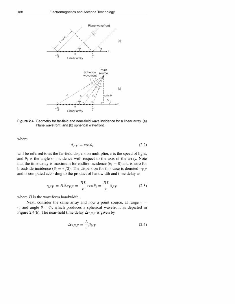
138 Electromagnetics and Antenna Technology
Plane wavefront
PointsourceSpherical
wavefront
L cos θ
i
θi θ
θi θ
L2– L
20
r i1
1 n N
ini i sin θi
iN
Linear array
L2– L
20
Linear array
z
(b)
(a)
z
r r r r
Figure 2.4 Geometry for far-field and near-field wave incidence for a linear array. (a)Plane wavefront, and (b) spherical wavefront.
whereβFF = cos θi (2.2)
will be referred to as the far-field dispersion multiplier, c is the speed of light,and θi is the angle of incidence with respect to the axis of the array. Notethat the time delay is maximum for endfire incidence (θi = 0) and is zero forbroadside incidence (θi = π/2). The dispersion for this case is denoted γFFand is computed according to the product of bandwidth and time delay as
γFF = B∆τFF =BL
ccos θi =
BL
cβFF (2.3)
where B is the waveform bandwidth.Next, consider the same array and now a point source, at range r =
ri and angle θ = θi, which produces a spherical wavefront as depicted inFigure 2.4(b). The near-field time delay ∆τNF is given by
∆τNF =L
cβNF (2.4)
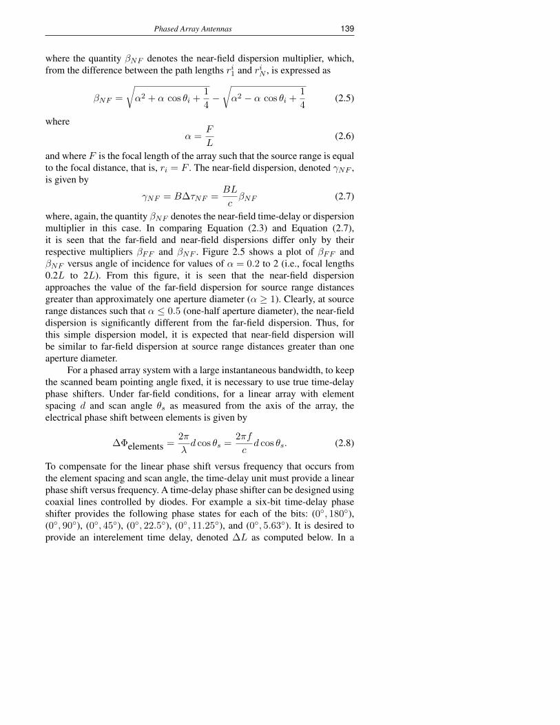
Phased Array Antennas 139
where the quantity βNF denotes the near-field dispersion multiplier, which,from the difference between the path lengths ri1 and riN , is expressed as
βNF =
√α2 + α cos θi +
1
4−√α2 − α cos θi +
1
4(2.5)
whereα =
F
L(2.6)
and where F is the focal length of the array such that the source range is equalto the focal distance, that is, ri = F . The near-field dispersion, denoted γNF ,is given by
γNF = B∆τNF =BL
cβNF (2.7)
where, again, the quantity βNF denotes the near-field time-delay or dispersionmultiplier in this case. In comparing Equation (2.3) and Equation (2.7),it is seen that the far-field and near-field dispersions differ only by theirrespective multipliers βFF and βNF . Figure 2.5 shows a plot of βFF andβNF versus angle of incidence for values of α = 0.2 to 2 (i.e., focal lengths0.2L to 2L). From this figure, it is seen that the near-field dispersionapproaches the value of the far-field dispersion for source range distancesgreater than approximately one aperture diameter (α ≥ 1). Clearly, at sourcerange distances such that α ≤ 0.5 (one-half aperture diameter), the near-fielddispersion is significantly different from the far-field dispersion. Thus, forthis simple dispersion model, it is expected that near-field dispersion willbe similar to far-field dispersion at source range distances greater than oneaperture diameter.
For a phased array system with a large instantaneous bandwidth, to keepthe scanned beam pointing angle fixed, it is necessary to use true time-delayphase shifters. Under far-field conditions, for a linear array with elementspacing d and scan angle θs as measured from the axis of the array, theelectrical phase shift between elements is given by
∆Φelements =2π
λd cos θs =
2πf
cd cos θs. (2.8)
To compensate for the linear phase shift versus frequency that occurs fromthe element spacing and scan angle, the time-delay unit must provide a linearphase shift versus frequency. A time-delay phase shifter can be designed usingcoaxial lines controlled by diodes. For example a six-bit time-delay phaseshifter provides the following phase states for each of the bits: (0, 180),(0, 90), (0, 45), (0, 22.5), (0, 11.25), and (0, 5.63). It is desired toprovide an interelement time delay, denoted ∆L as computed below. In a
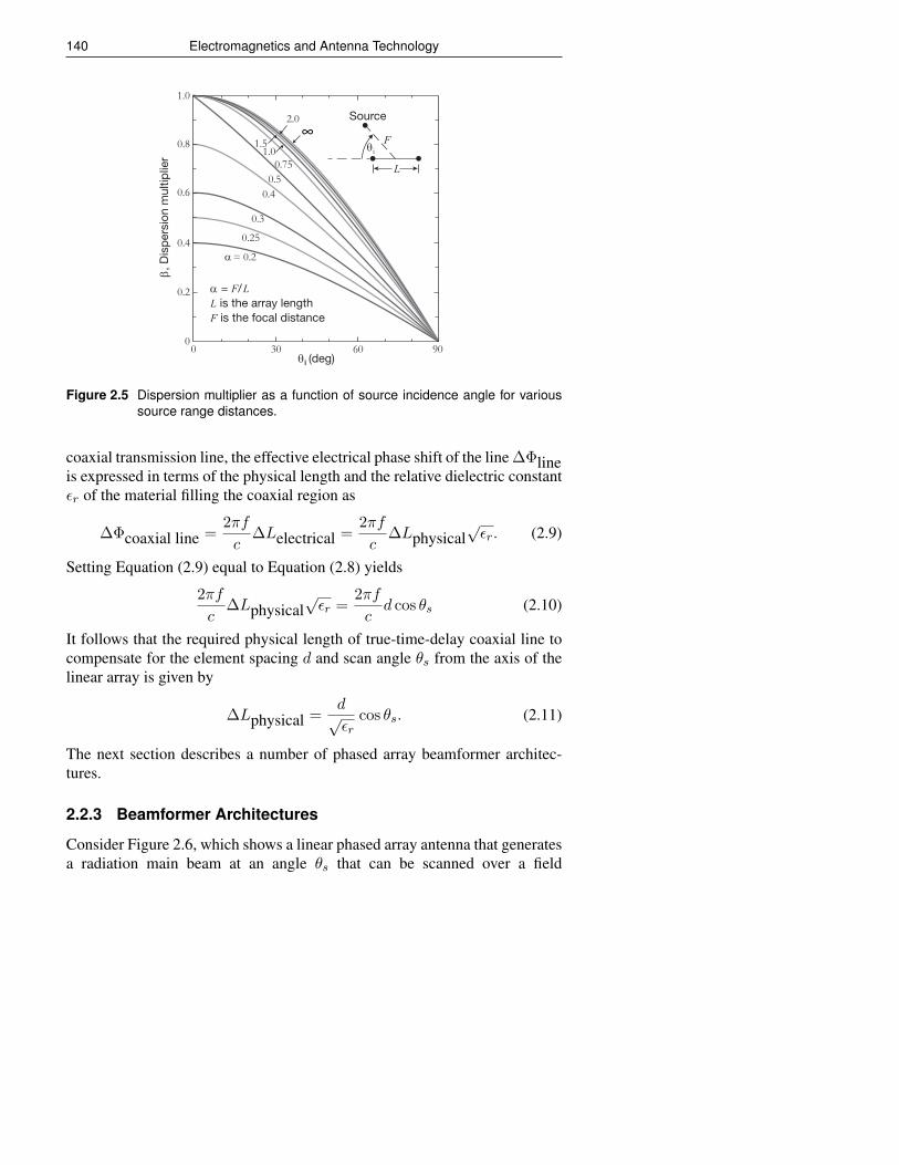
140 Electromagnetics and Antenna Technology
θi
θi (deg)
Source
F
2.0
1.51.0
0.750.5
0.4
0.3
0.25
α = 0.2
α = F/LL is the array lengthF is the focal distance
β, D
isp
ersi
on m
ultip
lier
00
0.2
0.4
0.6
0.8
1.0
30 60 90
L
∞
Figure 2.5 Dispersion multiplier as a function of source incidence angle for varioussource range distances.
coaxial transmission line, the effective electrical phase shift of the line ∆Φlineis expressed in terms of the physical length and the relative dielectric constantεr of the material filling the coaxial region as
∆Φcoaxial line =2πf
c∆Lelectrical =
2πf
c∆Lphysical
√εr. (2.9)
Setting Equation (2.9) equal to Equation (2.8) yields
2πf
c∆Lphysical
√εr =
2πf
cd cos θs (2.10)
It follows that the required physical length of true-time-delay coaxial line tocompensate for the element spacing d and scan angle θs from the axis of thelinear array is given by
∆Lphysical =d√εr
cos θs. (2.11)
The next section describes a number of phased array beamformer architec-tures.
2.2.3 Beamformer Architectures
Consider Figure 2.6, which shows a linear phased array antenna that generatesa radiation main beam at an angle θs that can be scanned over a field
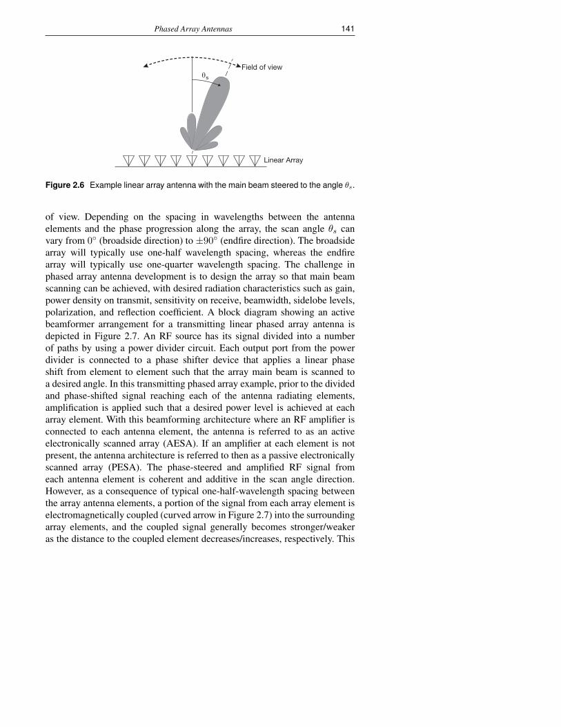
Phased Array Antennas 141
Linear Array
θs
Field of view
Figure 2.6 Example linear array antenna with the main beam steered to the angle θs.
of view. Depending on the spacing in wavelengths between the antennaelements and the phase progression along the array, the scan angle θs canvary from 0 (broadside direction) to ±90 (endfire direction). The broadsidearray will typically use one-half wavelength spacing, whereas the endfirearray will typically use one-quarter wavelength spacing. The challenge inphased array antenna development is to design the array so that main beamscanning can be achieved, with desired radiation characteristics such as gain,power density on transmit, sensitivity on receive, beamwidth, sidelobe levels,polarization, and reflection coefficient. A block diagram showing an activebeamformer arrangement for a transmitting linear phased array antenna isdepicted in Figure 2.7. An RF source has its signal divided into a numberof paths by using a power divider circuit. Each output port from the powerdivider is connected to a phase shifter device that applies a linear phaseshift from element to element such that the array main beam is scanned toa desired angle. In this transmitting phased array example, prior to the dividedand phase-shifted signal reaching each of the antenna radiating elements,amplification is applied such that a desired power level is achieved at eacharray element. With this beamforming architecture where an RF amplifier isconnected to each antenna element, the antenna is referred to as an activeelectronically scanned array (AESA). If an amplifier at each element is notpresent, the antenna architecture is referred to then as a passive electronicallyscanned array (PESA). The phase-steered and amplified RF signal fromeach antenna element is coherent and additive in the scan angle direction.However, as a consequence of typical one-half-wavelength spacing betweenthe array antenna elements, a portion of the signal from each array element iselectromagnetically coupled (curved arrow in Figure 2.7) into the surroundingarray elements, and the coupled signal generally becomes stronger/weakeras the distance to the coupled element decreases/increases, respectively. This
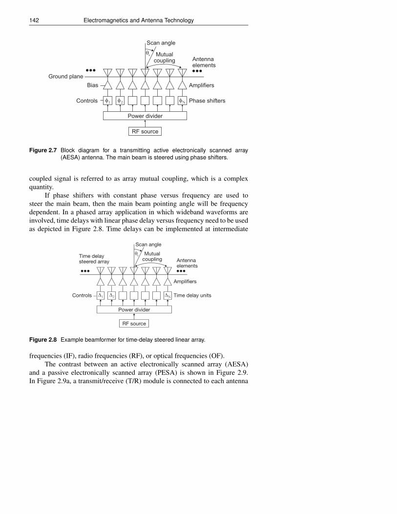
142 Electromagnetics and Antenna Technology
Controls Phase shifters
Amplifiers
Antennaelements
φ1
Power divider
φ2
RF source
φN
Scan angle
Mutualcoupling
θs
Ground planeBias
Figure 2.7 Block diagram for a transmitting active electronically scanned array(AESA) antenna. The main beam is steered using phase shifters.
coupled signal is referred to as array mutual coupling, which is a complexquantity.
If phase shifters with constant phase versus frequency are used tosteer the main beam, then the main beam pointing angle will be frequencydependent. In a phased array application in which wideband waveforms areinvolved, time delays with linear phase delay versus frequency need to be usedas depicted in Figure 2.8. Time delays can be implemented at intermediate
Controls Time delay units
Amplifiers
Antennaelements
∆1
Power divider
∆2
RF source
∆N
Scan angle
Mutualcoupling
θsTime delaysteered array
Figure 2.8 Example beamformer for time-delay steered linear array.
frequencies (IF), radio frequencies (RF), or optical frequencies (OF).The contrast between an active electronically scanned array (AESA)
and a passive electronically scanned array (PESA) is shown in Figure 2.9.In Figure 2.9a, a transmit/receive (T/R) module is connected to each antenna
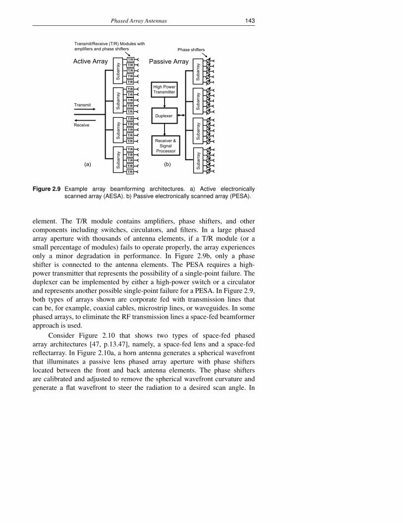
Phased Array Antennas 143
Duplexer
Receiver &Signal
Processor
High PowerTransmitter
Sub
arra
yS
ubar
ray
Sub
arra
yS
ubar
ray
Passive Array
Sub
arra
yS
ubar
ray
Sub
arra
yS
ubar
ray
T/RT/RT/R
T/R
T/R
T/RT/RT/R
T/R
T/R
T/RT/RT/R
T/R
T/R
T/RT/RT/R
T/R
T/R
Active Array
Transmit/Receive (T/R) Modules with amplifiers and phase shifters Phase shifters
Transmit
Receive
(a) (b)
Figure 2.9 Example array beamforming architectures. a) Active electronicallyscanned array (AESA). b) Passive electronically scanned array (PESA).
element. The T/R module contains amplifiers, phase shifters, and othercomponents including switches, circulators, and filters. In a large phasedarray aperture with thousands of antenna elements, if a T/R module (or asmall percentage of modules) fails to operate properly, the array experiencesonly a minor degradation in performance. In Figure 2.9b, only a phaseshifter is connected to the antenna elements. The PESA requires a high-power transmitter that represents the possibility of a single-point failure. Theduplexer can be implemented by either a high-power switch or a circulatorand represents another possible single-point failure for a PESA. In Figure 2.9,both types of arrays shown are corporate fed with transmission lines thatcan be, for example, coaxial cables, microstrip lines, or waveguides. In somephased arrays, to eliminate the RF transmission lines a space-fed beamformerapproach is used.
Consider Figure 2.10 that shows two types of space-fed phasedarray architectures [47, p.13.47], namely, a space-fed lens and a space-fedreflectarray. In Figure 2.10a, a horn antenna generates a spherical wavefrontthat illuminates a passive lens phased array aperture with phase shifterslocated between the front and back antenna elements. The phase shiftersare calibrated and adjusted to remove the spherical wavefront curvature andgenerate a flat wavefront to steer the radiation to a desired scan angle. In
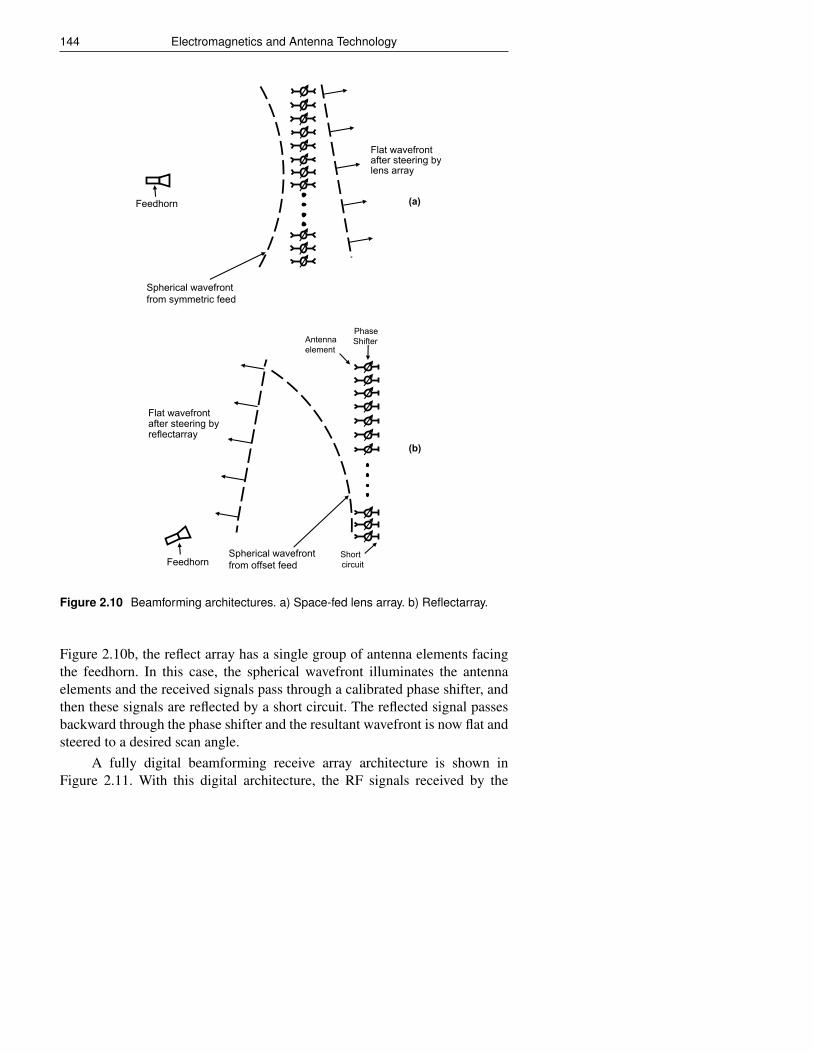
144 Electromagnetics and Antenna Technology
Spherical wavefrontfrom symmetric feed
Flat wavefront after steering by lens array
Feedhorn
Spherical wavefrontfrom offset feed
Flat wavefrontafter steering by reflectarray
FeedhornShortcircuit
PhaseShifterAntenna
element
(a)
(b)
Figure 2.10 Beamforming architectures. a) Space-fed lens array. b) Reflectarray.
Figure 2.10b, the reflect array has a single group of antenna elements facingthe feedhorn. In this case, the spherical wavefront illuminates the antennaelements and the received signals pass through a calibrated phase shifter, andthen these signals are reflected by a short circuit. The reflected signal passesbackward through the phase shifter and the resultant wavefront is now flat andsteered to a desired scan angle.
A fully digital beamforming receive array architecture is shown inFigure 2.11. With this digital architecture, the RF signals received by the
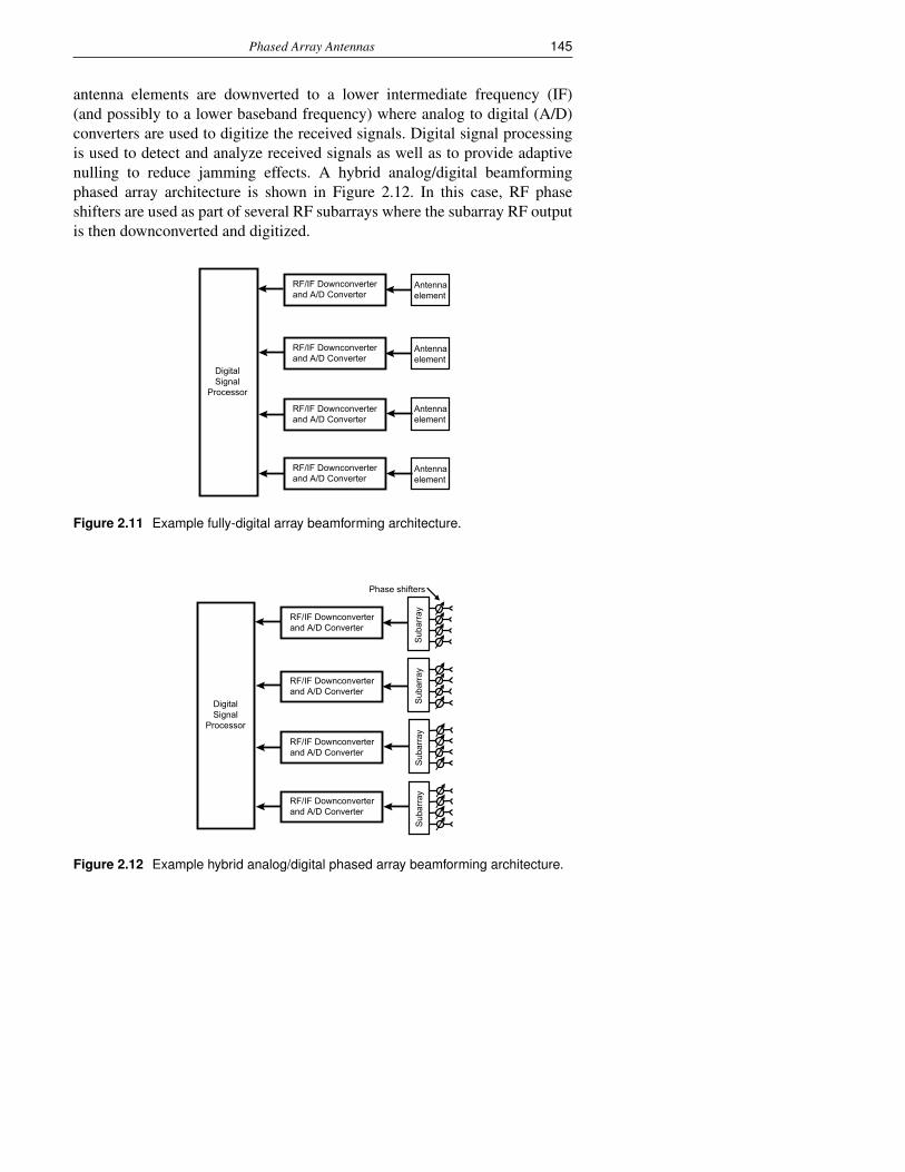
Phased Array Antennas 145
antenna elements are downverted to a lower intermediate frequency (IF)(and possibly to a lower baseband frequency) where analog to digital (A/D)converters are used to digitize the received signals. Digital signal processingis used to detect and analyze received signals as well as to provide adaptivenulling to reduce jamming effects. A hybrid analog/digital beamformingphased array architecture is shown in Figure 2.12. In this case, RF phaseshifters are used as part of several RF subarrays where the subarray RF outputis then downconverted and digitized.
DigitalSignal
Processor
RF/IF Downconverterand A/D Converter
RF/IF Downconverterand A/D Converter
RF/IF Downconverterand A/D Converter
RF/IF Downconverterand A/D Converter
Antennaelement
Antennaelement
Antennaelement
Antennaelement
Figure 2.11 Example fully-digital array beamforming architecture.
DigitalSignal
Processor
RF/IF Downconverterand A/D Converter
Sub
arra
yS
ubar
ray
Sub
arra
yS
ubar
ray
Phase shifters
RF/IF Downconverterand A/D Converter
RF/IF Downconverterand A/D Converter
RF/IF Downconverterand A/D Converter
Figure 2.12 Example hybrid analog/digital phased array beamforming architecture.
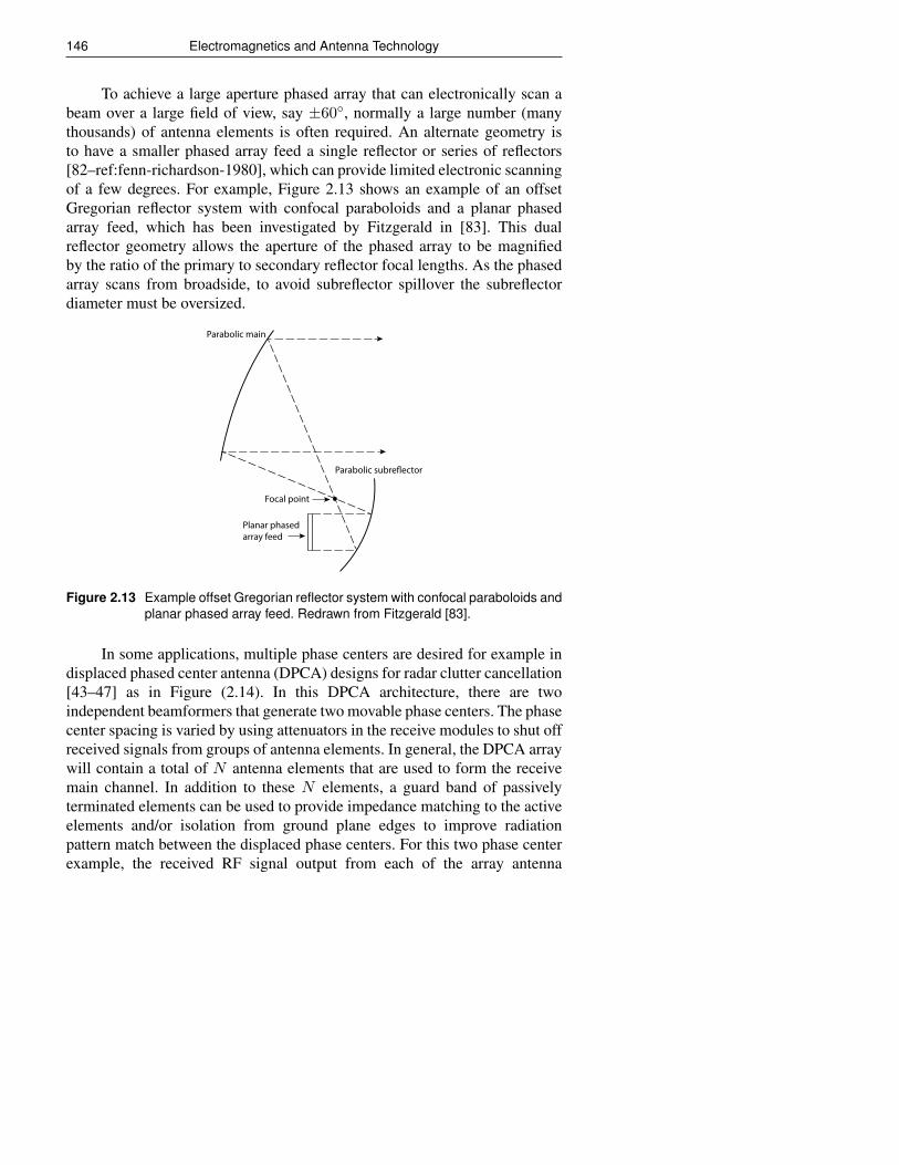
146 Electromagnetics and Antenna Technology
To achieve a large aperture phased array that can electronically scan abeam over a large field of view, say ±60, normally a large number (manythousands) of antenna elements is often required. An alternate geometry isto have a smaller phased array feed a single reflector or series of reflectors[82–ref:fenn-richardson-1980], which can provide limited electronic scanningof a few degrees. For example, Figure 2.13 shows an example of an offsetGregorian reflector system with confocal paraboloids and a planar phasedarray feed, which has been investigated by Fitzgerald in [83]. This dualreflector geometry allows the aperture of the phased array to be magnifiedby the ratio of the primary to secondary reflector focal lengths. As the phasedarray scans from broadside, to avoid subreflector spillover the subreflectordiameter must be oversized.
Parabolic main
Parabolic subreector
Planar phased array feed
Focal point
Figure 2.13 Example offset Gregorian reflector system with confocal paraboloids andplanar phased array feed. Redrawn from Fitzgerald [83].
In some applications, multiple phase centers are desired for example indisplaced phased center antenna (DPCA) designs for radar clutter cancellation[43–47] as in Figure (2.14). In this DPCA architecture, there are twoindependent beamformers that generate two movable phase centers. The phasecenter spacing is varied by using attenuators in the receive modules to shut offreceived signals from groups of antenna elements. In general, the DPCA arraywill contain a total of N antenna elements that are used to form the receivemain channel. In addition to these N elements, a guard band of passivelyterminated elements can be used to provide impedance matching to the activeelements and/or isolation from ground plane edges to improve radiationpattern match between the displaced phase centers. For this two phase centerexample, the received RF signal output from each of the array antenna
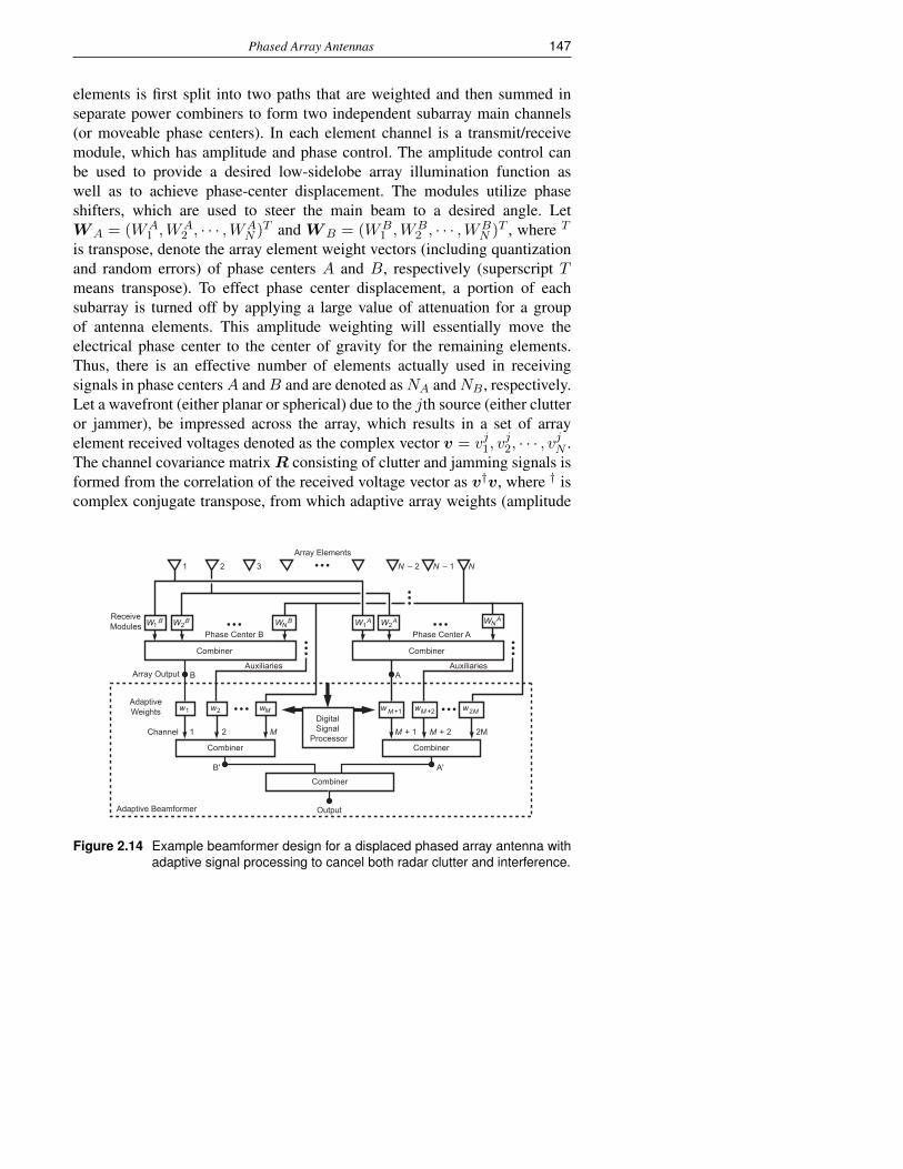
Phased Array Antennas 147
elements is first split into two paths that are weighted and then summed inseparate power combiners to form two independent subarray main channels(or moveable phase centers). In each element channel is a transmit/receivemodule, which has amplitude and phase control. The amplitude control canbe used to provide a desired low-sidelobe array illumination function aswell as to achieve phase-center displacement. The modules utilize phaseshifters, which are used to steer the main beam to a desired angle. LetWA = (WA
1 ,WA2 , · · · ,WA
N )T and WB = (WB1 ,W
B2 , · · · ,WB
N )T , where T
is transpose, denote the array element weight vectors (including quantizationand random errors) of phase centers A and B, respectively (superscript Tmeans transpose). To effect phase center displacement, a portion of eachsubarray is turned off by applying a large value of attenuation for a groupof antenna elements. This amplitude weighting will essentially move theelectrical phase center to the center of gravity for the remaining elements.Thus, there is an effective number of elements actually used in receivingsignals in phase centersA andB and are denoted asNA andNB , respectively.Let a wavefront (either planar or spherical) due to the jth source (either clutteror jammer), be impressed across the array, which results in a set of arrayelement received voltages denoted as the complex vector v = vj1, v
j2, · · · , v
jN .
The channel covariance matrixR consisting of clutter and jamming signals isformed from the correlation of the received voltage vector as v†v, where † iscomplex conjugate transpose, from which adaptive array weights (amplitude
1 2 3 – 2 – 1 N
Output
w1
W1B W2
B WNB W1
A W2A W A
w2 wM w w w
1 2 M + 1 + 2 2
A'B'
Auxiliaries AuxiliariesABArray Output
ReceiveModules
AdaptiveWeights
Phase Center B Phase Center A
Array ElementsNN
MM M
+1M +2M 2M
Channel
Adaptive Beamformer
N
Combiner Combiner
Combiner
Combiner Combiner
Digital Signal
Processor
Figure 2.14 Example beamformer design for a displaced phased array antenna withadaptive signal processing to cancel both radar clutter and interference.

148 Electromagnetics and Antenna Technology
and phase) are generated. The number of adaptive channels per phase centeris denoted M . For a sidelobe canceller M = 1 +Naux where Naux is thenumber of auxiliary channels in each phase center. This adaptive system hasM degrees of freedom in each phase center and, thus, a total of 2M degreesof freedom.
A simplified block diagram for an example transmit/receive (T/R)module is shown in Figure 2.15. By means of switches and proper timing, thephase shifter shown is used for both transmit and receive. In this diagram, theswitches are adjusted for the transmit mode. To protect the low noise amplifier(LNA) the combination of a circulator and a switched-in load provides highisolation from the high-power transmit signal. Many different architecturesexist for T/R modules, which are designed based on the system requirements.For example, in some radar applications the T/R modules must allow for dualpolarization and multiple phase center operation.
Recently, there has been considerable research in the area of multiple-input multiple-output (MIMO) arrays [63-65]. Figure 2.16 shows an artist’sconcept where a MIMO antenna system uses multiple transmit antennas andmultiple receive antennas to help mitigate multipath effects in communica-tions and radar applications.
To Beamformer
Other modules
Phased array control processor
Module
Transmit signal Amplifier Circulator
Poweramplifier
Command Registerand Driver (CR & D)
Low-noiseamplifier
Phaseshifter To and from
antenna
CR & D
Commandcomputation chip
Other modules
Prime power
Powerconditioning
AttenuatorCR & D
Receive signal
Load
Figure 2.15 Example transmit/receive (T/R) module block diagram.
Now that a number of beamforming architectures have been described,the next section describes basic array theory, which considers phased arrayscomposed of isotropic antenna elements.
Phased Array Antennas 149
Receive Antenna Array
Receive SignalsTransmit Signals
Transmit Antenna Array
Figure 2.16 Artist’s concept of a MIMO array system that consists of multiple transmitantennas and multiple receive antennas.
2.2.4 Arrays of Isotropic Antenna Elements
Consider the case of a two-dimensional N -element phased array of isotropicradiating antenna elements with the ejωt time-harmonic dependence of thecurrents suppressed, where ω = 2πf is the radian frequency, t is time, andf is the frequency. Referring to the geometry in Figures 2.2 and 2.3, thefar-field array radiation pattern, or array factor (AF) in this case, in termsof spherical coordinates (θ, φ), can be expressed by superposition of the Nradiating currents as
AF(θ, φ) =N∑n=1
inejΨn (2.12)
where in is the complex current induced in the nth radiating element,(xn, yn, zn) are the coordinates of the nth array element, and
Ψn = k sin θ(xn cosφ+ yn sinφ) + kzn cos θ (2.13)
where k = 2π/λ is the wavenumber with λ denoting the wavelength. In orderto electrically scan the main beam to a particular scan angle (θs, φs), thephasing Ψns of the element currents is set to be the negative value (phaseconjugate) of Ψn evaluated at (θs, φs), that is,
Ψns = −k sin θs(xn cosφs + yn sinφs)− kzn cos θs. (2.14)
The array currents in are expressed in complex form as
in = AnejΨns (2.15)

150 Electromagnetics and Antenna Technology
where An is the current amplitude illumination of the nth array element.Equation (2.15) is general in the sense that amplitude and phase quanti-zation and random errors of the transmit/receive modules can be included.Furthermore, Equations (2.13) and (2.14) allow errors in element positioning(∆xn,∆yn,∆zn) to be taken into account. The array factor for the electricallyscanned array can be written as
AF(θ, φ) =N∑n=1
Anej(Ψn+Ψns). (2.16)
If the current amplitudes are assumed to be uniform with unity amplitude,that is, An = 1, then when the observation angles (θ, φ) are equal to the scanangles (θs, φs), it follows from Equations (2.13) and (2.14) that Ψn + Ψns =0 and the array factor is evaluated as
AF(θs, φs) =N∑n=1
1 = N (2.17)
That is, for uniform illumination at scan-angle direction (θs, φs) the amplitudeof the array factor is equal to the number of array elements.
For a linear array oriented along the x axis, both yn and zn are zero. Thenwith φ = 0 using Equations (2.13) and (2.14), Equation (2.16) simplifies to
AF(θ, θs) =N∑n=1
Anejkxn(sin θ−sin θs). (2.18)
It should be noted that for the array factor given by Equation (2.18), since φwas set to zero, the angles θ and θs are allowed to take on positive and negativevalues.
A number of phased array illumination functions [5] can be used tocontrol the sidelobe levels and beamwidth of phased array antennas. Somecommon phased array illumination functions include uniform, binomial,triangular, cosine, Dolph-Chebyshev [89–91], and Taylor [92]. For example,uniformly illuminated arrays are typically used for transmit applications andhave a narrow beam with high first sidelobes (on the order of −13 dB relativeto the main beam maximum value). Compared to uniform illumination, thebinomial illumination has a broader beam with no sidelobes. The Dolph-Chebyshev illumination has low sidelobes at a constant, prescribed, level. TheTaylor illumination generates a narrow beam with controlled low sidelobes.Amplitude and phase quantization and random errors in the illuminationfunction can cause the sidelobes to degrade.

Phased Array Antennas 151
d
Array
z
x
θ
y
Figure 2.17 Linear array antenna of isotropic elements (point sources) spaced alongthe x axis.
Consider now a linear array with isotropic elements (point sources)that have spacing d along the x axis as shown in Figure 2.17. For theuniform illumination case An = 1, let the element position be quantified byxn = (n− 1)d and then let
u = kd(sin θ − sin θs). (2.19)
Equation (2.18) can now be simplified and then expanded as
AF(u) =N∑n=1
ejnu = 1 + eju + ej2u + · · ·+ ej(N−1)u (2.20)
Now multiply both sides of Equation (2.20) by eju which yields
AFeju = eju + ej2u + ej3u + · · ·+ ejNu (2.21)
Subtracting Equation (2.21) from (2.21) and rearranging yields
AF =ejNu − 1
eju − 1(2.22)
Factoring the exponentials in the numerator and denominator and convertingfrom exponentials to sines yields
AF = ej(N−1)u/2 sin(Nu/2)
sin(u/2)(2.23)
The maximum value of the array factor occurs at the main beam peak,which occurs when the denominator goes to zero, and this condition exists
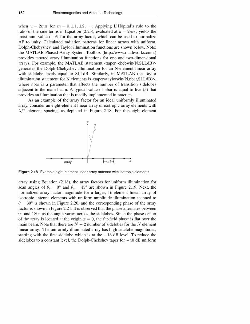
152 Electromagnetics and Antenna Technology
when u = 2mπ for m = 0,±1,±2, · · ·. Applying L’Hopital’s rule to theratio of the sine terms in Equation (2.23), evaluated at u = 2mπ, yields themaximum value of N for the array factor, which can be used to normalizeAF to unity. Calculated radiation patterns for linear arrays with uniform,Dolph-Chebyshev, and Taylor illumination functions are shown below. Note:the MATLAB Phased Array System Toolbox (http://www.mathworks.com.)provides tapered array illumination functions for one and two-dimensionalarrays. For example, the MATLAB statement <taper=chebwin(N,SLLdB)>generates the Dolph-Chebyshev illumination for an N-element linear arraywith sidelobe levels equal to SLLdB. Similarly, in MATLAB the Taylorillumination statement for N elements is <taper=taylorwin(N,nbar,SLLdB)>,where nbar is a parameter that affects the number of transition sidelobesadjacent to the main beam. A typical value of nbar is equal to five (5) thatprovides an illumination that is readily implemented in practice.
As an example of the array factor for an ideal uniformly illuminatedarray, consider an eight-element linear array of isotropic array elements withλ/2 element spacing, as depicted in Figure 2.18. For this eight-element
λ/2Array
z
x
θ
r
Figure 2.18 Example eight-element linear array antenna with isotropic elements.
array, using Equation (2.18), the array factors for uniform illumination forscan angles of θs = 0 and θs = 45 are shown in Figure 2.19. Next, thenormalized array factor magnitude for a larger, 16-element linear array ofisotropic antenna elements with uniform amplitude illumination scanned toθ = 30 is shown in Figure 2.20, and the corresponding phase of the arrayfactor is shown in Figure 2.21. It is observed that the phase alternates between0 and 180 as the angle varies across the sidelobes. Since the phase centerof the array is located at the origin x = 0, the far-field phase is flat over themain beam. Note that there are N − 2 number of sidelobes for the N elementlinear array. The uniformly illuminated array has high sidelobe magnitudes,starting with the first sidelobe which is at the −13 dB level. To reduce thesidelobes to a constant level, the Dolph-Chebshev taper for −40 dB uniform
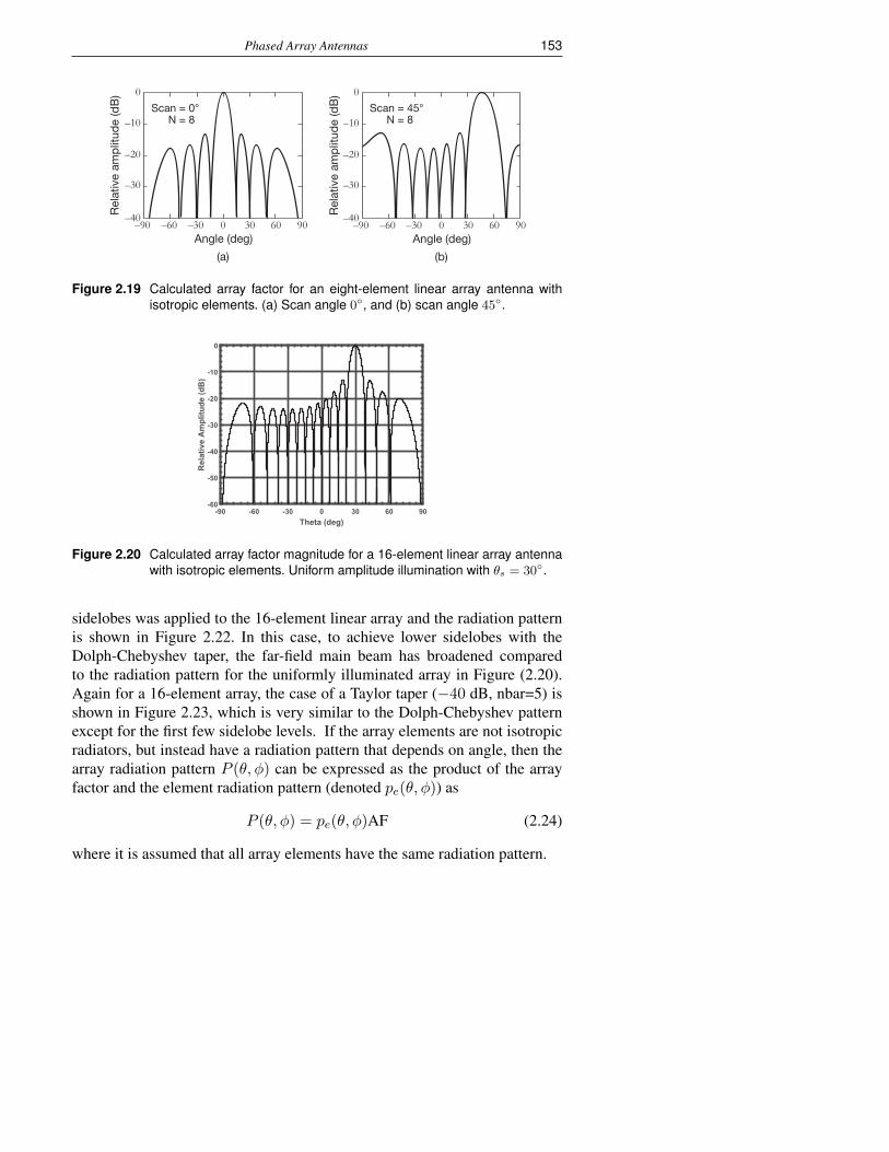
Phased Array Antennas 153
Angle (deg)
Scan = 0° N = 8
Scan = 45° N = 8
(a)
Rel
ativ
e am
plit
ude
(dB
)
–20
–10
0
–40
–30
30–30–60–90 60 900Angle (deg)
(b)
Rel
ativ
e am
plit
ude
(dB
)
–20
–10
0
–40
–30
30–30–60–90 60 900
Figure 2.19 Calculated array factor for an eight-element linear array antenna withisotropic elements. (a) Scan angle 0, and (b) scan angle 45.
-90 -60 -30 0 30 60 90Theta (deg)
-60
-50
-40
-30
-20
-10
0
Rel
ativ
e A
mpl
itude
(dB
)
Figure 2.20 Calculated array factor magnitude for a 16-element linear array antennawith isotropic elements. Uniform amplitude illumination with θs = 30.
sidelobes was applied to the 16-element linear array and the radiation patternis shown in Figure 2.22. In this case, to achieve lower sidelobes with theDolph-Chebyshev taper, the far-field main beam has broadened comparedto the radiation pattern for the uniformly illuminated array in Figure (2.20).Again for a 16-element array, the case of a Taylor taper (−40 dB, nbar=5) isshown in Figure 2.23, which is very similar to the Dolph-Chebyshev patternexcept for the first few sidelobe levels. If the array elements are not isotropicradiators, but instead have a radiation pattern that depends on angle, then thearray radiation pattern P (θ, φ) can be expressed as the product of the arrayfactor and the element radiation pattern (denoted pe(θ, φ)) as
P (θ, φ) = pe(θ, φ)AF (2.24)
where it is assumed that all array elements have the same radiation pattern.
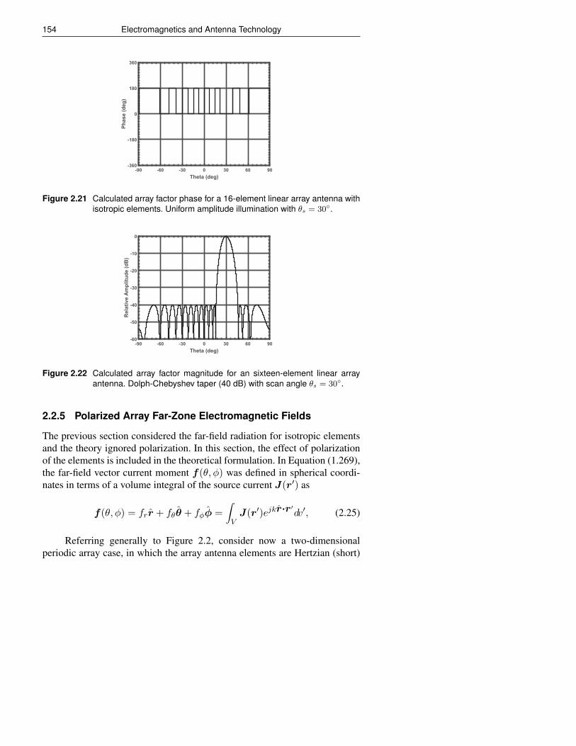
154 Electromagnetics and Antenna Technology
-90 -60 -30 0 30 60 90Theta (deg)
-360
-180
0
180
360
Phas
e (d
eg)
Figure 2.21 Calculated array factor phase for a 16-element linear array antenna withisotropic elements. Uniform amplitude illumination with θs = 30.
-90 -60 -30 0 30 60 90Theta (deg)
-60
-50
-40
-30
-20
-10
0
Rel
ativ
e A
mpl
itude
(dB
)
Figure 2.22 Calculated array factor magnitude for an sixteen-element linear arrayantenna. Dolph-Chebyshev taper (40 dB) with scan angle θs = 30.
2.2.5 Polarized Array Far-Zone Electromagnetic Fields
The previous section considered the far-field radiation for isotropic elementsand the theory ignored polarization. In this section, the effect of polarizationof the elements is included in the theoretical formulation. In Equation (1.269),the far-field vector current moment f(θ, φ) was defined in spherical coordi-nates in terms of a volume integral of the source current J(r′) as
f(θ, φ) = frr + fθθ + fφφ =
∫VJ(r′)ejkr·r′dv′, (2.25)
Referring generally to Figure 2.2, consider now a two-dimensionalperiodic array case, in which the array antenna elements are Hertzian (short)

Phased Array Antennas 155
-90 -60 -30 0 30 60 90Theta (deg)
-60
-50
-40
-30
-20
-10
0
Rel
ativ
e A
mpl
itude
(dB
)
Figure 2.23 Calculated array factor magnitude for an sixteen-element linear arrayantenna. Taylor taper (40 dB, nbar=5) with scan angle 30.
electric dipoles of length l and arbitrary polarization p that are located in arectangular lattice parallel to the xy plane at z = zo. Assume that the array hasNx elements in the x direction with interelement spacing dx and Ny elementsin the y direction with interelement spacing dy. The total number of elementsis equal toN = NxNy. Referring to Equation (2.14), let the electrical phasingof the nth Hertian dipole array element with position (xn, yn, zo) for the scandirection (θs, φs) be given by
Ψns = −kxn sin θs cosφs − kyn sin θs sinφs − kzo cos θs. (2.26)
In this case, the current density function J(r′) can be expressed in terms ofthe array element amplitude An = Inl and phase shift Ψns as
J(r′) = pN∑n=1
InlejΨnsδ(x′ − xn)δ(y′ − yn)δ(z′ − zo). (2.27)
The propagation unit vector in terms of the spherical coordinate angles (θ, φ)is given by
r = x sin θ cosφ+ y sin θ sinφ+ z cos θ (2.28)
and the source vector r′ is given by
r′ = xx′ + yy′ + zz′. (2.29)
The dot product of the propagation direction unit vector and the source vectoris equal to
r·r′ = x′ sin θ cosφ+ y′ sin θ sinφ+ z′ cos θ (2.30)
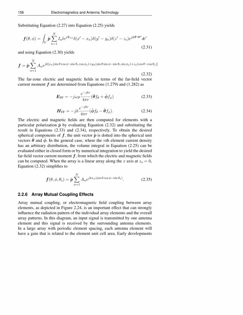
156 Electromagnetics and Antenna Technology
Substituting Equation (2.27) into Equation (2.25) yields
f(θ, φ) =
∫Vp
N∑n=1
InlejΨnsδ(x′ − xn)δ(y′ − yn)δ(z′ − zo)ejkr·r
′dv′
(2.31)and using Equation (2.30) yields
f = pN∑n=1
Anejk[xn(sin θ cosφ−sin θs cosφs)+yn(sin θ sinφ−sin θs sinφs)+zo(cos θ−cos θs)]
(2.32)The far-zone electric and magnetic fields in terms of the far-field vectorcurrent moment f are determined from Equations (1.279) and (1.282) as
EFF = −jωµe−jkr
4πr(θfθ + φfφ) (2.33)
HFF = −jk e−jkr
4πr(φfθ − θfφ). (2.34)
The electric and magnetic fields are then computed for elements with aparticular polarization p by evaluating Equation (2.32) and substituting theresult in Equations (2.33) and (2.34), respectively. To obtain the desiredspherical components of f , the unit vector p is dotted into the spherical unitvectors θ and φ. In the general case, where the nth element current densityhas an arbitrary distribution, the volume integral in Equation (2.25) can beevaluated either in closed form or by numerical integration to yield the desiredfar-field vector current moment f , from which the electric and magnetic fieldscan be computed. When the array is a linear array along the x axis at zo = 0,Equation (2.32) simplifies to
f(θ, φ, θs) = pN∑n=1
Anejkxn(sin θ cosφ−sin θs). (2.35)
2.2.6 Array Mutual Coupling Effects
Array mutual coupling, or electromagnetic field coupling between arrayelements, as depicted in Figure 2.24, is an important effect that can stronglyinfluence the radiation pattern of the individual array elements and the overallarray patterns. In this diagram, an input signal is transmitted by one antennaelement and this signal is received by the surrounding antenna elements.In a large array with periodic element spacing, each antenna element willhave a gain that is related to the element unit cell area. Early developments
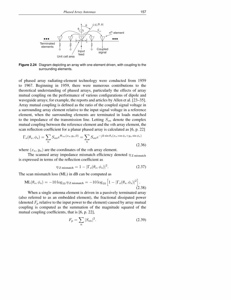
Phased Array Antennas 157
Terminatedelements
Coupledsignal
nth elementSon
ge(θ, φ)
Inputfeed
Unit cell area
φθ
Figure 2.24 Diagram depicting an array with one element driven, with coupling to thesurrounding elements.
of phased array radiating-element technology were conducted from 1959to 1967. Beginning in 1959, there were numerous contributions to thetheoretical understanding of phased arrays, particularly the effects of arraymutual coupling on the performance of various configurations of dipole andwaveguide arrays; for example, the reports and articles by Allen et al. [23–35].Array mutual coupling is defined as the ratio of the coupled signal voltage ina surrounding array element relative to the input signal voltage in a referenceelement, when the surrounding elements are terminated in loads matchedto the impedance of the transmission line. Letting Son denote the complexmutual coupling between the reference element and the nth array element, thescan reflection coefficient for a planar phased array is calculated as [6, p. 22]
Γo(θs, φs) =∑n
SoneΨns(xn,yn,0) =
∑n
Sone−jk sin θs(xn cosφs+yn sinφs)
(2.36)where (xn, yn) are the coordinates of the nth array element.
The scanned array impedance mismatch efficiency denoted η Z mismatchis expressed in terms of the reflection coefficient as
η Z mismatch = 1− |Γo(θs, φs)|2. (2.37)
The scan mismatch loss (ML) in dB can be computed as
ML(θs, φs) = −10 log10 η Z mismatch = −10 log10
[1− |Γo(θs, φs)|2
].
(2.38)When a single antenna element is driven in a passively terminated array
(also referred to as an embedded element), the fractional dissipated power(denoted Fp relative to the input power to the element) caused by array mutualcoupling is computed as the summation of the magnitude squared of themutual coupling coefficients, that is [6, p. 22],
Fp =∑n
|Son|2. (2.39)
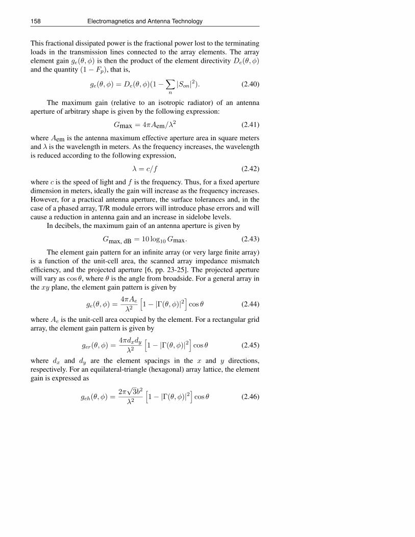
158 Electromagnetics and Antenna Technology
This fractional dissipated power is the fractional power lost to the terminatingloads in the transmission lines connected to the array elements. The arrayelement gain ge(θ, φ) is then the product of the element directivity De(θ, φ)and the quantity (1− Fp), that is,
ge(θ, φ) = De(θ, φ)(1−∑n
|Son|2). (2.40)
The maximum gain (relative to an isotropic radiator) of an antennaaperture of arbitrary shape is given by the following expression:
Gmax = 4πAem/λ2 (2.41)
where Aem is the antenna maximum effective aperture area in square metersand λ is the wavelength in meters. As the frequency increases, the wavelengthis reduced according to the following expression,
λ = c/f (2.42)
where c is the speed of light and f is the frequency. Thus, for a fixed aperturedimension in meters, ideally the gain will increase as the frequency increases.However, for a practical antenna aperture, the surface tolerances and, in thecase of a phased array, T/R module errors will introduce phase errors and willcause a reduction in antenna gain and an increase in sidelobe levels.
In decibels, the maximum gain of an antenna aperture is given by
Gmax, dB = 10 log10Gmax. (2.43)
The element gain pattern for an infinite array (or very large finite array)is a function of the unit-cell area, the scanned array impedance mismatchefficiency, and the projected aperture [6, pp. 23-25]. The projected aperturewill vary as cos θ, where θ is the angle from broadside. For a general array inthe xy plane, the element gain pattern is given by
ge(θ, φ) =4πAeλ2
[1− |Γ(θ, φ)|2
]cos θ (2.44)
where Ae is the unit-cell area occupied by the element. For a rectangular gridarray, the element gain pattern is given by
ger(θ, φ) =4πdxdyλ2
[1− |Γ(θ, φ)|2
]cos θ (2.45)
where dx and dy are the element spacings in the x and y directions,respectively. For an equilateral-triangle (hexagonal) array lattice, the elementgain is expressed as
geh(θ, φ) =2π√
3b2
λ2
[1− |Γ(θ, φ)|2
]cos θ (2.46)
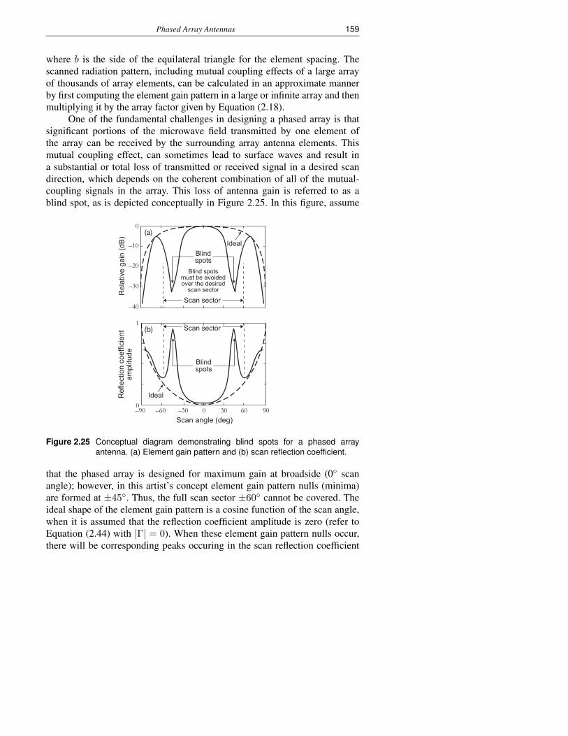
Phased Array Antennas 159
where b is the side of the equilateral triangle for the element spacing. Thescanned radiation pattern, including mutual coupling effects of a large arrayof thousands of array elements, can be calculated in an approximate mannerby first computing the element gain pattern in a large or infinite array and thenmultiplying it by the array factor given by Equation (2.18).
One of the fundamental challenges in designing a phased array is thatsignificant portions of the microwave field transmitted by one element ofthe array can be received by the surrounding array antenna elements. Thismutual coupling effect, can sometimes lead to surface waves and result ina substantial or total loss of transmitted or received signal in a desired scandirection, which depends on the coherent combination of all of the mutual-coupling signals in the array. This loss of antenna gain is referred to as ablind spot, as is depicted conceptually in Figure 2.25. In this figure, assume
–30
–40
1
0
–20
–10
0
0 30–30–60–90 60 90
Rel
ativ
e ga
in (d
B)
Ref
lect
ion
coef
ficie
ntam
plitu
de
Blindspots
Scan sector
Blindspots
Scan angle (deg)
Ideal
Scan sector
Ideal(a)
(b)
Blind spotsmust be avoidedover the desired
scan sector
Figure 2.25 Conceptual diagram demonstrating blind spots for a phased arrayantenna. (a) Element gain pattern and (b) scan reflection coefficient.
that the phased array is designed for maximum gain at broadside (0 scanangle); however, in this artist’s concept element gain pattern nulls (minima)are formed at ±45. Thus, the full scan sector ±60 cannot be covered. Theideal shape of the element gain pattern is a cosine function of the scan angle,when it is assumed that the reflection coefficient amplitude is zero (refer toEquation (2.44) with |Γ| = 0). When these element gain pattern nulls occur,there will be corresponding peaks occuring in the scan reflection coefficient
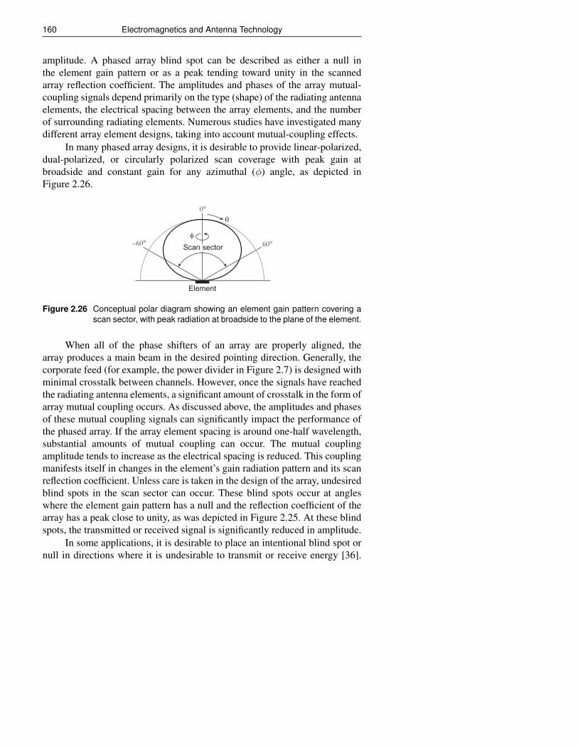
160 Electromagnetics and Antenna Technology
amplitude. A phased array blind spot can be described as either a null inthe element gain pattern or as a peak tending toward unity in the scannedarray reflection coefficient. The amplitudes and phases of the array mutual-coupling signals depend primarily on the type (shape) of the radiating antennaelements, the electrical spacing between the array elements, and the numberof surrounding radiating elements. Numerous studies have investigated manydifferent array element designs, taking into account mutual-coupling effects.
In many phased array designs, it is desirable to provide linear-polarized,dual-polarized, or circularly polarized scan coverage with peak gain atbroadside and constant gain for any azimuthal (φ) angle, as depicted inFigure 2.26.
Scan sector
Element
60°–60°
0°θ
φ
Figure 2.26 Conceptual polar diagram showing an element gain pattern covering ascan sector, with peak radiation at broadside to the plane of the element.
When all of the phase shifters of an array are properly aligned, thearray produces a main beam in the desired pointing direction. Generally, thecorporate feed (for example, the power divider in Figure 2.7) is designed withminimal crosstalk between channels. However, once the signals have reachedthe radiating antenna elements, a significant amount of crosstalk in the form ofarray mutual coupling occurs. As discussed above, the amplitudes and phasesof these mutual coupling signals can significantly impact the performance ofthe phased array. If the array element spacing is around one-half wavelength,substantial amounts of mutual coupling can occur. The mutual couplingamplitude tends to increase as the electrical spacing is reduced. This couplingmanifests itself in changes in the element’s gain radiation pattern and its scanreflection coefficient. Unless care is taken in the design of the array, undesiredblind spots in the scan sector can occur. These blind spots occur at angleswhere the element gain pattern has a null and the reflection coefficient of thearray has a peak close to unity, as was depicted in Figure 2.25. At these blindspots, the transmitted or received signal is significantly reduced in amplitude.
In some applications, it is desirable to place an intentional blind spot ornull in directions where it is undesirable to transmit or receive energy [36].
Phased Array Antennas 161
For example, Figure 2.27 shows an example of a broadside-null radiationpattern that could be generated by either a monopole or a uniform-current loopantenna element in an array environment over a ground plane. These types of
Circle (azimuth)“Omnidirectional”
Shaped(elevation)
θ
φ
z
x y
Figure 2.27 Artist depiction of a monopole-type radiation pattern for an element in aphased array antenna.
elements could be useful when broadside radiation is undesirable, such as inreducing broadside clutter and jamming in the case of a spaceborne radar [45,46]. As the radar beam is steered away from θ = 0 (broadside) toward θ =60, the conventional broadside-peak-type element radiation pattern drops off,but the broadside-null-type element radiation pattern increases to a peak atabout θ = 45 to 50.
2.2.7 Power Density and Array Gain
The effective isotropic radiated power, denoted EIRP, of an aperture is givenby the product of the antenna gain Gmax and the transmitter power Ptdelivered to the antenna as
EIRP = PtGt. (2.47)
Note that the power transmitted by the antenna is usually less than the powerdelivered by the generator feeding the antenna. This difference in power isattributed to any RF losses between the generator and the antenna, as wellas any mismatch loss resulting from the reflection coefficient at the antennaterminals.
If the overall antenna aperture is assumed to be an array of identicalelements, the aperture can be divided into element apertures, which are alsoreferred to as element unit cells (see Figure 2.24). For a largeN -element arraywith an effective aperture Aem, the unit cell area is equal to Aem/N . If the
162 Electromagnetics and Antenna Technology
embedded element gain patterns are either computed or measured, the arraygain can be computed as follows. At range distance r, the embedded-elementradiated power density, denoted Pde, resulting from the element transmitpower (input power to the element) and embedded-element gain is given by[15]
Pde =Ptege(θ, φ)
4πr2(2.48)
and solving for ge,
ge = 4πr2PdePte
. (2.49)
In the far field, the plane-wave power density of the element is given in termsof the array-element electric field intensity Ee(θ, φ) as
Pde =|Ee(θ, φ)|2
120π. (2.50)
Substituting Equation (2.50) in Equation (2.49) and simplifying yields
ge(θ, φ) =r2
30
|Ee(θ, φ)|2
Pte. (2.51)
Thus, it follows that
|Ee(θ, φ)| =√
30
r
√ge(θ, φ)
√Pte. (2.52)
The element gain pattern, ge(θ, φ) includes the effect of array mutual couplingand mismatch losses.
The transmit power of the nth element is proportional to A2n, and using
this relation in Equation (2.52) yields
|Een(θ, φ)| =√
30
r
√gen(θ, φ)An. (2.53)
To compute the maximum gain of an array at a particular scan angle(θs, φs), by superposition the electric-field contributions for the embeddedelements can be summed as
Earray, max =
√30
r
∑n
√genAn. (2.54)
Now, following along the lines of Equation (2.51), the array gain can beexpressed as
Garray, max =r2
30
|Earray, max|2
Pt, array(2.55)
Phased Array Antennas 163
where
Pt, array =N∑n=1
A2n. (2.56)
Substituting Equations (2.54) and (2.56) in Equation (2.55) and simpli-fying yields
Garray, max =|∑Nn=1√genAn|2∑N
n=1A2n
. (2.57)
For the case of a large array with uniform array illumination (with unityamplitude at each array element), it can be assumed that all of the elementshave the same element gain pattern (i.e., gen = ge) and Equation (2.57)reduces to
Garray, max(θs, φs) = ge(θs, φs)N. (2.58)
For uniform illumination, the array gain is equal to the element gain times thenumber of array elements. If the array illumination is not uniform, then a taperefficiency must be included in computing the array gain from the element gain.
To compute the array gain pattern from the element electric fieldversus angle (θ, φ), the element phase pattern Ψen(θ, φ) (either calculatedor measured) must be used, that is,
Een(θ, φ) = |Een(θ, φ)|ejΨen(θ,φ). (2.59)
The array pattern Earray is then obtained by the superposition of theindividual array element patterns with the desired array amplitude taper andwith proper phasing of the array to steer the main beam in a desired direction.Thus,
Earray(θ, φ) =∑n
Een(θ, φ)ejΨns (2.60)
or from Equation (2.59)
Earray(θ, φ) =∑n
|Een(θ, φ)|ej(Ψen+Ψns) (2.61)
and using Equation (2.53) yields
Earray(θ, φ) =
√30
r
∑n
√gen(θ, φ)Ane
j(Ψen+Ψns). (2.62)
The array gain as a function of angle can then be computed from the electricfield as
Garray(θ, φ) =r2
30
|Earray(θ, φ)|2
Pt, array. (2.63)
164 Electromagnetics and Antenna Technology
Substituting Equations (2.56) and (2.62) in Equation (2.63) yields the arraygain in terms of the element gain and element phase functions and the arrayillumination, that is,
Garray(θ, φ) =|∑n
√gen(θ, φ)Ane
j(Ψen+Ψns)|2∑nA
2n
. (2.64)
In designing phased array antennas, the maximum electrical spacing dbetween the elements of a phased array is usually chosen to avoid gratinglobes (multiple peaks) according to the following condition [9]
d
λh<
1
1 + sin |θs|(2.65)
where λh is the wavelength at the highest frequency and θs is the scan anglefrom broadside. This equation is readily derived by setting the exponentialargument of the array factor in Equation (2.18) equal to −2π and using apositive scan angle and taking the observation angle as the endfire angle−90,where the grating lobe first occurs, and then solving for d/λ. Typically, themaximum array-element spacing d is more tightly constrained to keep thefirst null of the endfire grating lobe at the edge of visible space. In practice,the endfire grating lobe should be kept at least one half-power beamwidthaway from visible space. For many wide-angle scanning phased arrays, theelectrical spacing is often chosen to be close to one-half wavelength forelements on a rectangular or triangular grid.
The next four sections describe methods that are used in computingelectromagnetic fields of antennas, including array mutual coupling effectsand scattering from obstacles. The discussion begins with a description ofelectromagnetic field equivalence principles in Section 2.3. In the subsequentsection, the reciprocity theorem for antennas is derived. To determine themutual coupling between an antenna and surrounding antennas in an array orinteraction with surrounding structures, a generalized integral equation knownas the reaction integral equation is then developed in Section 2.5, which isbased on the equivalence principle and the reciprocity theorem for antennas.The reaction integral equation is used in analyzing antennas and phased arraysby the method of moments, which is discussed in Section 2.6.
2.3 Equivalence Principles
To describe the various forms of equivalence principles, assume an antennawith arbitrary impressed electric and magnetic currents, J i and M i, respec-tively, in free space (region 1) radiating in the presence of a homogeneous
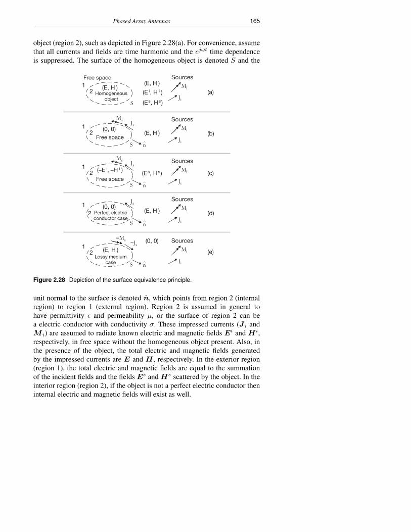
Phased Array Antennas 165
object (region 2), such as depicted in Figure 2.28(a). For convenience, assumethat all currents and fields are time harmonic and the ejωt time dependenceis suppressed. The surface of the homogeneous object is denoted S and the
(d)
(c)
Sources
(Es, Hs)1
2
S
(–E i, –H i )
Free space
Mi
Ms
Ji
Js
n^
(e)
Sources
(E, H )1
2
S
Perfect electricconductor case
Mi
Ji
Js
n^
(b)
Sources
(E, H )1
2
S
(0, 0) Mi
Ms
Ji
Js
n^
(a)
Sources(E, H )1
2
S
(E, H )Homogeneous
object
Mi
Ji
Sources1
2
S
Mi
–Ms
Ji
–Js
n^Lossy medium
case
(E, H )
(0, 0)
(E i, H i )
(Es, Hs)
Free space
Free space
(0, 0)
Figure 2.28 Depiction of the surface equivalence principle.
unit normal to the surface is denoted n, which points from region 2 (internalregion) to region 1 (external region). Region 2 is assumed in general tohave permittivity ε and permeability µ, or the surface of region 2 can bea electric conductor with conductivity σ. These impressed currents (J i andM i) are assumed to radiate known electric and magnetic fields Ei and H i,respectively, in free space without the homogeneous object present. Also, inthe presence of the object, the total electric and magnetic fields generatedby the impressed currents are E and H , respectively. In the exterior region(region 1), the total electric and magnetic fields are equal to the summationof the incident fields and the fields Es and Hs scattered by the object. In theinterior region (region 2), if the object is not a perfect electric conductor theninternal electric and magnetic fields will exist as well.
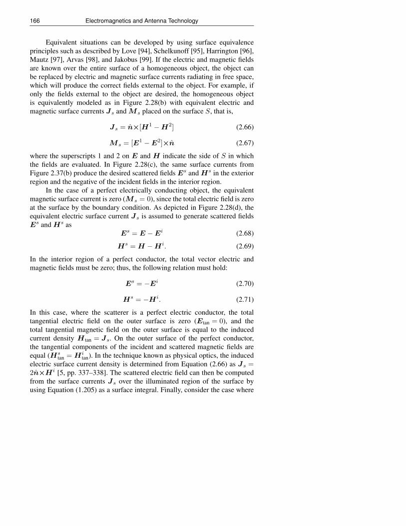
166 Electromagnetics and Antenna Technology
Equivalent situations can be developed by using surface equivalenceprinciples such as described by Love [94], Schelkunoff [95], Harrington [96],Mautz [97], Arvas [98], and Jakobus [99]. If the electric and magnetic fieldsare known over the entire surface of a homogeneous object, the object canbe replaced by electric and magnetic surface currents radiating in free space,which will produce the correct fields external to the object. For example, ifonly the fields external to the object are desired, the homogeneous objectis equivalently modeled as in Figure 2.28(b) with equivalent electric andmagnetic surface currents Js andM s placed on the surface S, that is,
Js = n×[H1 −H2] (2.66)
M s = [E1 −E2]×n (2.67)
where the superscripts 1 and 2 on E and H indicate the side of S in whichthe fields are evaluated. In Figure 2.28(c), the same surface currents fromFigure 2.37(b) produce the desired scattered fields Es and Hs in the exteriorregion and the negative of the incident fields in the interior region.
In the case of a perfect electrically conducting object, the equivalentmagnetic surface current is zero (M s = 0), since the total electric field is zeroat the surface by the boundary condition. As depicted in Figure 2.28(d), theequivalent electric surface current Js is assumed to generate scattered fieldsEs andHs as
Es = E −Ei (2.68)
Hs = H −H i. (2.69)
In the interior region of a perfect conductor, the total vector electric andmagnetic fields must be zero; thus, the following relation must hold:
Es = −Ei (2.70)
Hs = −H i. (2.71)
In this case, where the scatterer is a perfect electric conductor, the totaltangential electric field on the outer surface is zero (Etan = 0), and thetotal tangential magnetic field on the outer surface is equal to the inducedcurrent density H tan = Js. On the outer surface of the perfect conductor,the tangential components of the incident and scattered magnetic fields areequal (Hs
tan = H itan). In the technique known as physical optics, the induced
electric surface current density is determined from Equation (2.66) as Js =2n×H i [5, pp. 337–338]. The scattered electric field can then be computedfrom the surface currents Js over the illuminated region of the surface byusing Equation (1.205) as a surface integral. Finally, consider the case where
Phased Array Antennas 167
the object is a homogeneous lossy medium as depicted in Figure 2.28(e).In this case, the negative of the equivalent currents produce the desiredfields inside the object in which the dielectric and magnetic properties of thematerial must be used in computing the internal fields. Now that the necessaryequivalence conditions have been described, the next step in developing amethod of moments formulation is to derive the reciprocity theorem.
2.4 Reciprocity Theorem
Let there be two sets of electric and magnetic sources Ja, Ma and J b, M b,which produce the fields Ea, Ha and Eb, Hb, respectively. The Lorentzreciprocity theorem [5] is derived in the following manner starting withMaxwell’s equations in time-harmonic form as:
∇×Ea = −Ma − jωµ′Ha (2.72)
∇×Ha = Ja + jωε′Ea (2.73)
∇×Eb = −M b − jωµ′Hb (2.74)
∇×Hb = J b + jωε′Eb (2.75)
Now, take the divergence of the difference between the vector cross productsof the fields from the a and b sources and apply the vector identity
∇·(A×B) = B·(∇×A)−A·(∇×B). (2.76)
which yields after eliminating the terms involving the dot products of thevector fields
−∇·(Ea×Hb −Eb×Ha) = Ea·J b −Ha·M b −Eb·Ja +Hb·Ma
(2.77)which is the Lorentz reciprocity theorem in differential form. Now, taking thevolume integral of both sides of Equation (2.77) and applying the divergencetheorem to the left-hand side yields∫
V∇·Adv =
∮SA·ds (2.78)
yields−∮S∇·(Ea×Hb −Eb×Ha)·ds =∫
V (Ea·J b −Ha·M b −Eb·Ja +Hb·Ma)dv(2.79)
which is the integral form of the Lorentz reciprocity theorem.

168 Electromagnetics and Antenna Technology
The integral form of the Lorentz reciprocity theorem in a source-freeregion is expressed as∫∫
S(Ea×Hb −Eb×Ha)·ds = 0. (2.80)
That is, if the surface S does not enclose sources, the volume integral on theright side of Equation (2.79) is zero. Next, consider the case of a radiatingantenna with source currents contained within a finite volume. In this case,if the surface S is allowed to extend to infinity, the antenna radiated fieldsat infinity in the surface integral are attenuated to zero and now the left sideof Equation (2.79) is zero. Thus, the reciprocity theorem for antennas can beexpressed as∫∫∫
V(Ea·J b −Ha·M b −Eb·Ja +Hb·Ma)dv = 0 (2.81)
where the volume integration extends over all space including the antennasource currents in the constrained finite volume.
2.5 Reaction Integral Equation
The generalized reaction integral equation is derived from the reciprocitytheorem for antennas expressed by Equation (2.81). By definition, the reactionof field a on source current b is given by [101, 102, p. 118]
< a, b >=
∫∫∫V
(Ea·J b −Ha·M b)dv. (2.82)
By reciprocity, the reaction of field a on source current b is the same as thereaction of field b on source current a, that is,
< a, b >=< b, a > . (2.83)
Let a test source with currents Jm and Mm be placed within thescatterer volume, which has now been replaced by the original ambientmedium. These currents radiate the fields Em and Hm in the ambientmedium. It is desired to compute the reaction between the test source currentswith the total electric and magnetic fields within the volume within the surfaceS. Since the total electric and magnetic fields are equal to zero within thescatterer, the reaction between the test source and total fields is zero. Thus, wecan write ∫∫∫
mJm·(Es +Ei)dv = 0 (2.84)

Phased Array Antennas 169
∫∫∫mMm·(Hs +H i)dv = 0. (2.85)
To be consistent with the minus sign in the reciprocity theorem, the differencebetween Equations (2.84) and (2.85) is taken, which results in∫∫∫
m(Jm·Es −Mm·Hs)dv +
∫∫∫m
(Jm·Ei −Mm·H i)dv = 0 (2.86)
where the volume integration is over the volume of the test source. In termsof surface integrals and surface currents, Equation (2.86) becomes∫∫
S(Jms·Es −Mms·Hs)ds+
∫∫S
(Jms·Ei −Mms·H i)ds = 0 (2.87)
where m = 1, 2, 3, · · · , N , Jms is the mth electric surface current, andMms
is the mth magnetic surface current. Equation (2.87) is the desired reactionintegral equation. The next section shows how Equation (2.87) can be solvedusing the method of moments.
2.6 Method of Moments
The reaction integral equation expressed by Equation (2.87) can be solvedusing the method of moments for the vector currents, from which quantitiessuch as the antenna input impedance and gain radiation patterns can becomputed. In general, when one is applying the method of moments, eachantenna analysis geometry requires special considerations [102–109]. Byusing the equivalence principle as shown in Figure 2.28, the moment methodsolution is considerably simplified for antenna problems involving onlyelectric conductors and, thus, only vector electric currents J are assumednonzero, andM = 0.
In the method of moments, the unknown vector electric surface currentdensity Js is expressed initially as a summation of n surface currents Jnwhere
Jn = inBn (2.88)
in which the current coefficients in are complex in general and they arethe N unknown coefficients to be determined, and there are N vector basisfunctions bn (also referred to as expansion or interpolation functions). Thus,the unknown vector surface current density can be expressed as
Js =N∑n=1
Jn =N∑n=1
inbn. (2.89)
170 Electromagnetics and Antenna Technology
It is desired to react an mth vector testing current source tm (also referredto as a vector weighting source) with the radiated field from the nth basisfunction bn. The electric field from the nth basis function can be expressedas the scattered field Es
n(Jn), where it is understood that the electric field isdetermined by an integral operating on the nth electric-current function Jn.This integral operation can be expressed as
Lop(Jn) = Esn(Jn) (2.90)
where Lop is the integral operator. For example, the electric field Esn(Jn)
can be determined using a two-step approach in which the integral inEquation (1.197) is evaluated and is then substituted into Equation (1.192).The integral operation on the current is a linear operator, that is, superpositionapplies and scalar quantities within the integral can be factored out of theintegral. It is noted that the total scattered field is given by
Es =N∑n=1
Esn(Jn). (2.91)
Thus, it follows from Equation (2.87) that
N∑n=1
∫∫Stm·Es
n(Jn)ds+
∫∫Stm·Eids = 0, (2.92)
which is the electric-field integral equation (EFIE), which is valid for openand closed surfaces. Using Equations (2.89) and (2.91) and the linearity of theintegral operator, it follows that Equation (2.92) can be rewritten as
∫∫Stm·Eids = −
N∑n=1
in
∫∫Stm·Es
n(bn)ds (2.93)
where the nth complex current coefficient in has been factored out of thedouble integration. The basis functions bn can be chosen typically to havean overlapping piecewise sinusoidal or triangular amplitude distribution, andthese basis functions are known to provide an accurate representation ofcurrents that flow on antennas and surrounding structures. In the case of apiecewise-sinusoidal basis function of arbitrary unit vector orientation p alongan arbitrary p axis (for example, p could be the z axis), the basis function takesthe following form [83, 85],
bn(p) = pnsin k(p− pn−1)
sin k(pn − pn−1)pn−1 ≤ p ≤ pn (2.94)
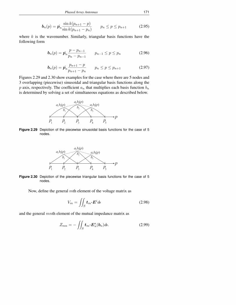
Phased Array Antennas 171
bn(p) = pnsin k(pn+1 − p)sin k(pn+1 − pn)
pn ≤ p ≤ pn+1 (2.95)
where k is the wavenumber. Similarly, triangular basis functions have thefollowing form
bn(p) = pnp− pn−1
pn − pn−1pn−1 ≤ p ≤ pn (2.96)
bn(p) = pnpn+1 − ppn+1 − pn
pn ≤ p ≤ pn+1 (2.97)
Figures 2.29 and 2.30 show examples for the case where there are 5 nodes and3 overlapping (piecewise) sinusoidal and triangular basis functions along thep axis, respectively. The coefficient an that multiplies each basis function bnis determined by solving a set of simultaneous equations as described below.
pp
1p
4p
2p
3p
5
b2b1 b3
b1a1 (p)b2a2 (p)
b3a3 (p)
Figure 2.29 Depiction of the piecewise sinusoidal basis functions for the case of 5nodes.
pp
1p
4p
2p
3p
5
b2b1 b3
b1a1 (p)b2a2 (p)
b3a3 (p)
Figure 2.30 Depiction of the piecewise triangular basis functions for the case of 5nodes.
Now, define the general mth element of the voltage matrix as
Vm =
∫∫Stm·Eids (2.98)
and the general mnth element of the mutual impedance matrix as
Zmn = −∫∫
Stm·Es
n(bn)ds. (2.99)

172 Electromagnetics and Antenna Technology
Note: since the testing and basis functions are typically normalized bydividing by the terminal current, the units of the voltage matrix and impedancematrix are in volts and ohms, respectively. A Galerkin’s formulation isobtained by using testing functions t that are equal to the basis functions b. Itnow follows that
Vm =N∑n=1
inZmn m = 1, 2, . . . , N (2.100)
where Vm is the voltage excitation and Zmn is the open-circuit mutualimpedance between current elements m and n, expressed as the matrix Z.These expressions can be combined in terms of the applied voltage excitationvector V , the impedance matrix Z, and unknown current vector i to give thematrix equation
V = Zi; (2.101)
that is,
V1 = Z11i1 + Z12i2 + · · ·+ Z1N iN
V2 = Z21i1 + Z22i2 + · · ·+ Z2N iN
.
. (2.102)
.
VN = ZN1i1 + ZN2i2 + · · ·+ ZNN iN .
The unknown current coefficients in, n = 1, 2, . . . , N are found by matrixinversion from
i = Z−1V (2.103)
or by lower-triangular/upper-triangular (LU) matrix decomposition, for exam-ple. For phased array antenna analysis, the current responses for multiplebeam-steering voltage vectors are readily computed since the impedancematrix inversion or LU decomposition needs to be performed only once for agiven antenna geometry.
The voltage source model chosen at the antenna terminals is typically adelta gap generator. This model assumes that the impressed electric field existsonly at the antenna element terminals. In this case, the voltage generators canbe defined to be one volt in amplitude at the terminals of each array element.
If a general skew-symmetric lattice is assumed for the dipole array asdepicted in Figure 2.39, then the required steering phase for an element in the
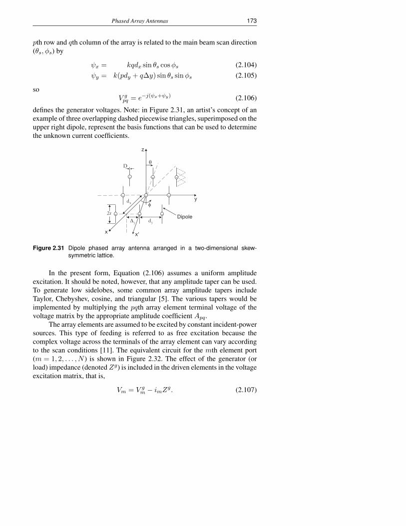
Phased Array Antennas 173
pth row and qth column of the array is related to the main beam scan direction(θs, φs) by
ψx = kqdx sin θs cosφs (2.104)ψy = k(pdy + q∆y) sin θs sinφs (2.105)
soV gpq = e−j(ψx+ψy) (2.106)
defines the generator voltages. Note: in Figure 2.31, an artist’s concept of anexample of three overlapping dashed piecewise triangles, superimposed on theupper right dipole, represent the basis functions that can be used to determinethe unknown current coefficients.
Dipoledy
dx
∆y
φ
z
x x'
y
~ ~ ~
~
~~~
D
~~
θ
2
Figure 2.31 Dipole phased array antenna arranged in a two-dimensional skew-symmetric lattice.
In the present form, Equation (2.106) assumes a uniform amplitudeexcitation. It should be noted, however, that any amplitude taper can be used.To generate low sidelobes, some common array amplitude tapers includeTaylor, Chebyshev, cosine, and triangular [5]. The various tapers would beimplemented by multiplying the pqth array element terminal voltage of thevoltage matrix by the appropriate amplitude coefficient Apq.
The array elements are assumed to be excited by constant incident-powersources. This type of feeding is referred to as free excitation because thecomplex voltage across the terminals of the array element can vary accordingto the scan conditions [11]. The equivalent circuit for the mth element port(m = 1, 2, . . . , N ) is shown in Figure 2.32. The effect of the generator (orload) impedance (denotedZg) is included in the driven elements in the voltageexcitation matrix, that is,
Vm = V gm − imZg. (2.107)
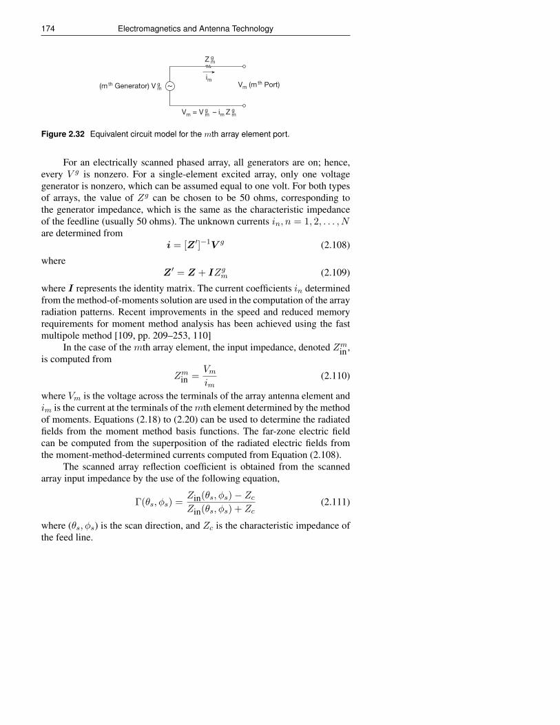
174 Electromagnetics and Antenna Technology
(mth Generator) V gm
Vm
im
Z gm
Vm = V gm – im Z
gm
(mth Port)~
Figure 2.32 Equivalent circuit model for the mth array element port.
For an electrically scanned phased array, all generators are on; hence,every V g is nonzero. For a single-element excited array, only one voltagegenerator is nonzero, which can be assumed equal to one volt. For both typesof arrays, the value of Zg can be chosen to be 50 ohms, corresponding tothe generator impedance, which is the same as the characteristic impedanceof the feedline (usually 50 ohms). The unknown currents in, n = 1, 2, . . . , Nare determined from
i = [Z ′]−1V g (2.108)
whereZ ′ = Z + IZgm (2.109)
where I represents the identity matrix. The current coefficients in determinedfrom the method-of-moments solution are used in the computation of the arrayradiation patterns. Recent improvements in the speed and reduced memoryrequirements for moment method analysis has been achieved using the fastmultipole method [109, pp. 209–253, 110]
In the case of the mth array element, the input impedance, denoted Zmin ,is computed from
Zmin =Vmim
(2.110)
where Vm is the voltage across the terminals of the array antenna element andim is the current at the terminals of themth element determined by the methodof moments. Equations (2.18) to (2.20) can be used to determine the radiatedfields from the moment method basis functions. The far-zone electric fieldcan be computed from the superposition of the radiated electric fields fromthe moment-method-determined currents computed from Equation (2.108).
The scanned array reflection coefficient is obtained from the scannedarray input impedance by the use of the following equation,
Γ(θs, φs) =Zin(θs, φs)− ZcZin(θs, φs) + Zc
(2.111)
where (θs, φs) is the scan direction, and Zc is the characteristic impedance ofthe feed line.
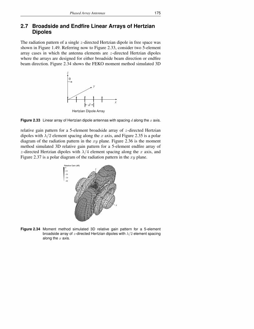
Phased Array Antennas 175
2.7 Broadside and Endfire Linear Arrays of HertzianDipoles
The radiation pattern of a single z-directed Hertzian dipole in free space wasshown in Figure 1.49. Referring now to Figure 2.33, consider two 5-elementarray cases in which the antenna elements are z-directed Hertzian dipoleswhere the arrays are designed for either broadside beam direction or endfirebeam direction. Figure 2.34 shows the FEKO moment method simulated 3D
d
Hertzian Dipole Array
z
x
θ
y
Figure 2.33 Linear array of Hertzian dipole antennas with spacing d along the x axis.
relative gain pattern for a 5-element broadside array of z-directed Hertziandipoles with λ/2 element spacing along the x axis, and Figure 2.35 is a polardiagram of the radiation pattern in the xy plane. Figure 2.36 is the momentmethod simulated 3D relative gain pattern for a 5-element endfire array ofz-directed Hertzian dipoles with λ/4 element spacing along the x axis, andFigure 2.37 is a polar diagram of the radiation pattern in the xy plane.
Relative Gain (dB)
−40
−20
0
−10
−30
x
y
z
Figure 2.34 Moment method simulated 3D relative gain pattern for a 5-elementbroadside array of z-directed Hertzian dipoles with λ/2 element spacingalong the x axis.
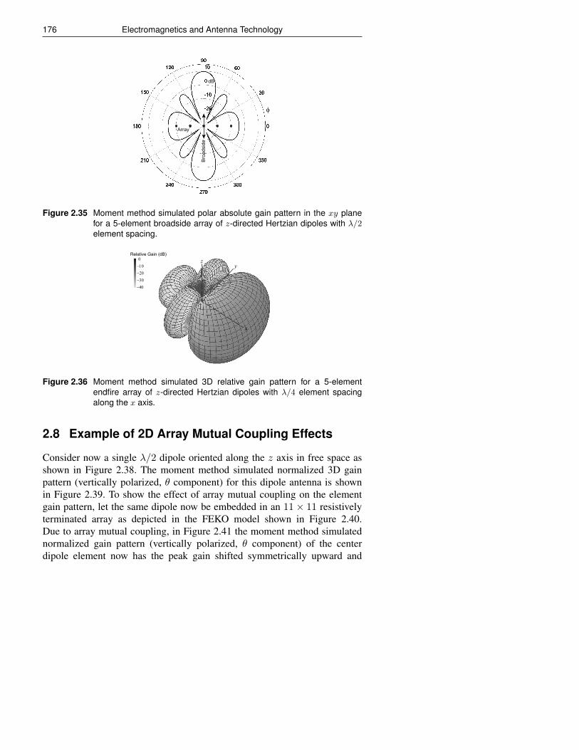
176 Electromagnetics and Antenna Technology
dB
φ
Bro
adsi
de
Array
Figure 2.35 Moment method simulated polar absolute gain pattern in the xy planefor a 5-element broadside array of z-directed Hertzian dipoles with λ/2element spacing.
Relative Gain (dB)
−40
−20
0
−10
−30
zy
x
Figure 2.36 Moment method simulated 3D relative gain pattern for a 5-elementendfire array of z-directed Hertzian dipoles with λ/4 element spacingalong the x axis.
2.8 Example of 2D Array Mutual Coupling Effects
Consider now a single λ/2 dipole oriented along the z axis in free space asshown in Figure 2.38. The moment method simulated normalized 3D gainpattern (vertically polarized, θ component) for this dipole antenna is shownin Figure 2.39. To show the effect of array mutual coupling on the elementgain pattern, let the same dipole now be embedded in an 11× 11 resistivelyterminated array as depicted in the FEKO model shown in Figure 2.40.Due to array mutual coupling, in Figure 2.41 the moment method simulatednormalized gain pattern (vertically polarized, θ component) of the centerdipole element now has the peak gain shifted symmetrically upward and

Phased Array Antennas 177
φ
dB
Array Endfire
Figure 2.37 Moment method simulated polar absolute gain pattern in the xy plane fora 5-element endfire array of z-directed Hertzian dipoles with λ/4 elementspacing.
downward from the xy plane, and thus has reduced relative gain in the xyplane. There is a natual null in the direction of the z axis, which means thedipole element in this orientation has a natural blind spot.
xy
z
Figure 2.38 Moment method model for a λ/2 dipole in free space.
2.9 Swept-Back Dipole Array Measurements andSimulations
2.9.1 Introduction
Dipole phased array antennas are commonly used in radar and communica-tions applications, and these elements have been researched extensively inthe literature [23–26, 32–34, 48, 111–116]. Linear dipoles can be designed toradiate or receive linear polarization. Crossed-dipoles can operate with dualpolarization or circular polarization. Dipoles typically have straight arms thatare parallel to a conducting ground plane; however, for wide-angle pattern
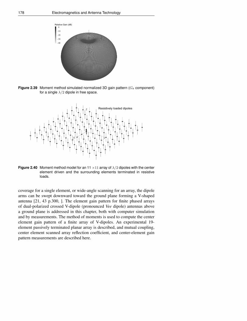
178 Electromagnetics and Antenna Technology
Relative Gain (dB)
−40
−20
0
−10
−30
Figure 2.39 Moment method simulated normalized 3D gain pattern (Gθ component)for a single λ/2 dipole in free space.
x
z
y
Resistively loaded dipoles
Figure 2.40 Moment method model for an 11×11 array of λ/2 dipoles with the centerelement driven and the surrounding elements terminated in resistiveloads.
coverage for a single element, or wide-angle scanning for an array, the dipolearms can be swept downward toward the ground plane forming a V-shapedantenna [21, 43 p.300, ]. The element gain pattern for finite phased arraysof dual-polarized crossed V-dipole (pronounced Vee dipole) antennas abovea ground plane is addressed in this chapter, both with computer simulationand by measurements. The method of moments is used to compute the centerelement gain pattern of a finite array of V-dipoles. An experimental 19-element passively terminated planar array is described, and mutual coupling,center element scanned array reflection coefficient, and center-element gainpattern measurements are described here.
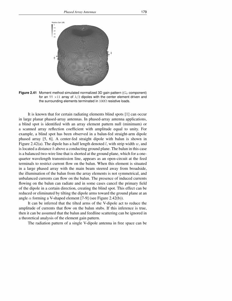
Phased Array Antennas 179
Relative Gain (dB)
−40
−20
0
−10
−30
Figure 2.41 Moment method simulated normalized 3D gain pattern (Gθ component)for an 11 ×11 array of λ/2 dipoles with the center element driven andthe surrounding elements terminated in 100Ω resistive loads.
It is known that for certain radiating elements blind spots [1] can occurin large planar phased-array antennas. In phased-array antenna applications,a blind spot is identified with an array element pattern null (minimum) ora scanned array reflection coefficient with amplitude equal to unity. Forexample, a blind spot has been observed in a balun-fed straight-arm dipolephased array [5, 6]. A center-fed straight dipole with balun is shown inFigure 2.42(a). The dipole has a half length denoted l, with strip width w, andis located a distance h above a conducting ground plane. The balun in this caseis a balanced two-wire line that is shorted at the ground plane, which for a one-quarter wavelength transmission line, appears as an open-circuit at the feedterminals to restrict current flow on the balun. When this element is situatedin a large phased array with the main beam steered away from broadside,the illumination of the balun from the array elements is not symmetrical, andunbalanced currents can flow on the balun. The presence of induced currentsflowing on the balun can radiate and in some cases cancel the primary fieldof the dipole in a certain direction, creating the blind spot. This effect can bereduced or eliminated by tilting the dipole arms toward the ground plane at anangle α forming a V-shaped element [7-9] (see Figure 2.42(b)).
It can be inferred that the tilted arms of the V-dipole act to reduce theamplitude of currents that flow on the balun stubs. If this inference is true,then it can be assumed that the balun and feedline scattering can be ignored ina theoretical analysis of the element gain pattern.
The radiation pattern of a single V-dipole antenna in free space can be

180 Electromagnetics and Antenna Technology
V-Dipole
Ground Plane
Ground Plane
Coaxial Feed
Coaxial Feed
Balun
w
Balun
(a)
(b)
Straight Dipole
h
h
w
α
430822_m_1.aiFigure 2.42 Balun-fed dipoles above a ground plane. (a) Straight arm, and (b) V-dipole. c© 1988 IEEE [9].
computed as follows. Schelkunoff and Friis have given an expression for theradiation pattern of a dipole arm with sinusoidal current distribution [10]. Ifit is assumed that the dipole arm is oriented in the z′ direction, the radiationfield pattern is expressed as
Eθ =j30itsin kl
ejkl cos θ′j cos θ′ sin kl − cos kl
sin θ′(2.112)
where k = 2π/λ, and λ is the wavelength. From the diagram shown inFigure 2.43 for a V-dipole in free space, the pertinent angles θ′L for the lefthalf dipole and θ′R for the right half of the V-dipole, in terms of the angles θand α, are given by
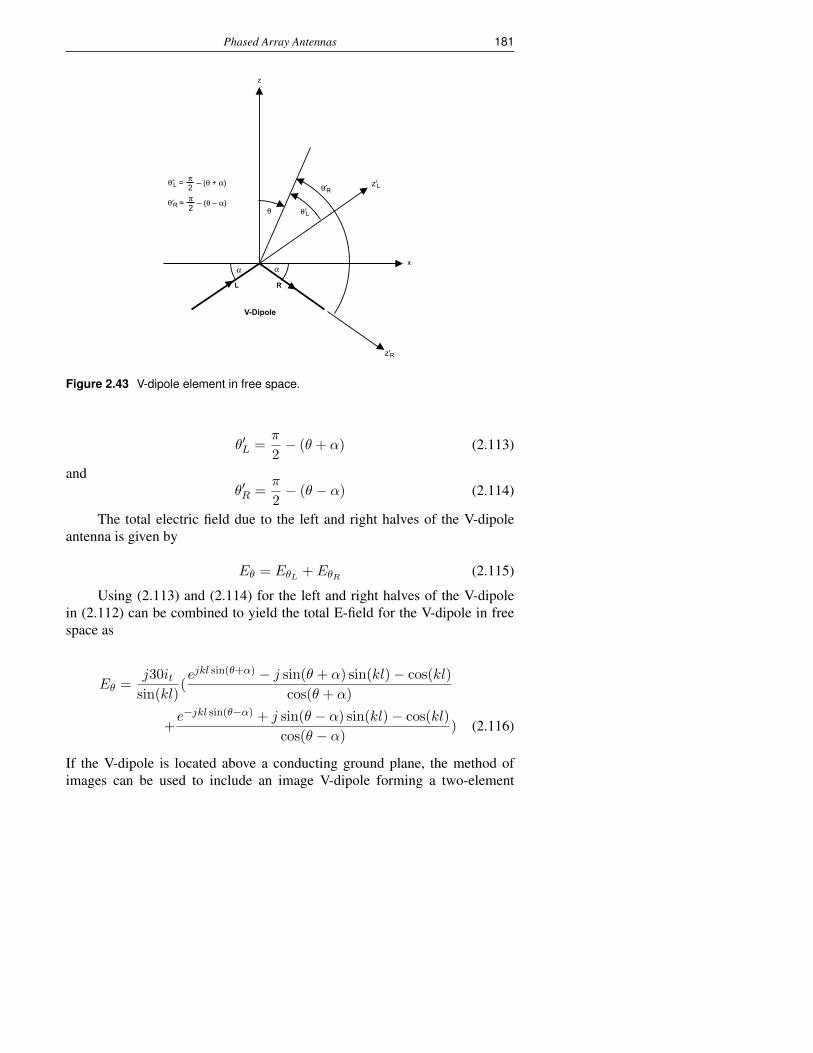
Phased Array Antennas 181
V-Dipole
z
x
L R
θ
α α
θ′L
θ′L z′L
z′R
θ′R
430822_m_2.ai
= – (θ + α)
θ′R = – (θ – α)
π2π2
Figure 2.43 V-dipole element in free space.
θ′L =π
2− (θ + α) (2.113)
andθ′R =
π
2− (θ − α) (2.114)
The total electric field due to the left and right halves of the V-dipoleantenna is given by
Eθ = EθL + EθR (2.115)
Using (2.113) and (2.114) for the left and right halves of the V-dipolein (2.112) can be combined to yield the total E-field for the V-dipole in freespace as
Eθ =j30it
sin(kl)(ejkl sin(θ+α) − j sin(θ + α) sin(kl)− cos(kl)
cos(θ + α)
+e−jkl sin(θ−α) + j sin(θ − α) sin(kl)− cos(kl)
cos(θ − α)) (2.116)
If the V-dipole is located above a conducting ground plane, the method ofimages can be used to include an image V-dipole forming a two-element
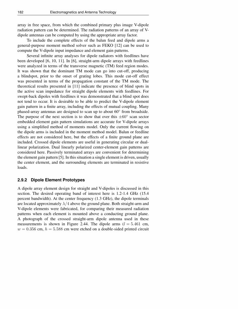
182 Electromagnetics and Antenna Technology
array in free space, from which the combined primary plus image V-dipoleradiation pattern can be determined. The radiation patterns of an array of V-dipole antennas can be computed by using the appropriate array factor.
To include the complete effects of the balun feed and dipole arms ageneral-purpose moment method solver such as FEKO [12] can be used tocompute the V-dipole input impedance and element gain patterns.
Several infinite array analyses for dipole radiators with feedlines havebeen developed [6, 10, 11]. In [6], straight-arm dipole arrays with feedlineswere analyzed in terms of the transverse magnetic (TM) feed region modes.It was shown that the dominant TM mode can go into cut-off, producinga blindspot, prior to the onset of grating lobes. This mode cut-off effectwas presented in terms of the propagation constant of the TM mode. Thetheoretical results presented in [11] indicate the presence of blind spots inthe active scan impedance for straight dipole elements with feedlines. Forswept-back dipoles with feedlines it was demonstrated that a blind spot doesnot tend to occur. It is desirable to be able to predict the V-dipole elementgain pattern in a finite array, including the effects of mutual coupling. Manyphased-array antennas are designed to scan up to about 60 from broadside.The purpose of the next section is to show that over this ±60 scan sectorembedded element gain pattern simulations are accurate for V-dipole arraysusing a simplified method of moments model. Only the current flowing onthe dipole arms is included in the moment method model. Balun or feedlineeffects are not considered here, but the effects of a finite ground plane areincluded. Crossed dipole elements are useful in generating circular or dual-linear polarization. Dual linearly polarized center-element gain patterns areconsidered here. Passively terminated arrays are convenient for determiningthe element gain pattern [5]. In this situation a single element is driven, usuallythe center element, and the surrounding elements are terminated in resistiveloads.
2.9.2 Dipole Element Prototypes
A dipole array element design for straight and V-dipoles is discussed in thissection. The desired operating band of interest here is 1.2-1.4 GHz (15.4percent bandwidth). At the center frequency (1.3 GHz), the dipole terminalsare located approximately λ/4 above the ground plane. Both straight-arm andV-dipole elements were fabricated, for comparing their measured radiationpatterns when each element is mounted above a conducting ground plane.A photograph of the crossed straight-arm dipole antenna used in thesemeasurements is shown in Figure 2.44. The dipole arms (l = 5.461 cm,w = 0.356 cm, h = 5.588 cm were etched on a double-sided printed circuit
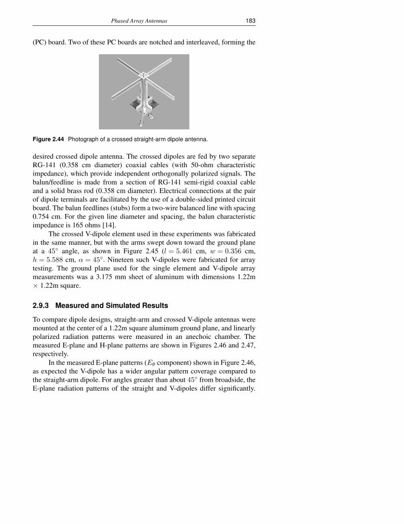
Phased Array Antennas 183
(PC) board. Two of these PC boards are notched and interleaved, forming the
Figure 2.44 Photograph of a crossed straight-arm dipole antenna.
desired crossed dipole antenna. The crossed dipoles are fed by two separateRG-141 (0.358 cm diameter) coaxial cables (with 50-ohm characteristicimpedance), which provide independent orthogonally polarized signals. Thebalun/feedline is made from a section of RG-141 semi-rigid coaxial cableand a solid brass rod (0.358 cm diameter). Electrical connections at the pairof dipole terminals are facilitated by the use of a double-sided printed circuitboard. The balun feedlines (stubs) form a two-wire balanced line with spacing0.754 cm. For the given line diameter and spacing, the balun characteristicimpedance is 165 ohms [14].
The crossed V-dipole element used in these experiments was fabricatedin the same manner, but with the arms swept down toward the ground planeat a 45 angle, as shown in Figure 2.45 (l = 5.461 cm, w = 0.356 cm,h = 5.588 cm, α = 45. Nineteen such V-dipoles were fabricated for arraytesting. The ground plane used for the single element and V-dipole arraymeasurements was a 3.175 mm sheet of aluminum with dimensions 1.22m× 1.22m square.
2.9.3 Measured and Simulated Results
To compare dipole designs, straight-arm and crossed V-dipole antennas weremounted at the center of a 1.22m square aluminum ground plane, and linearlypolarized radiation patterns were measured in an anechoic chamber. Themeasured E-plane and H-plane patterns are shown in Figures 2.46 and 2.47,respectively.
In the measured E-plane patterns (Eθ component) shown in Figure 2.46,as expected the V-dipole has a wider angular pattern coverage compared tothe straight-arm dipole. For angles greater than about 45 from broadside, theE-plane radiation patterns of the straight and V-dipoles differ significantly.
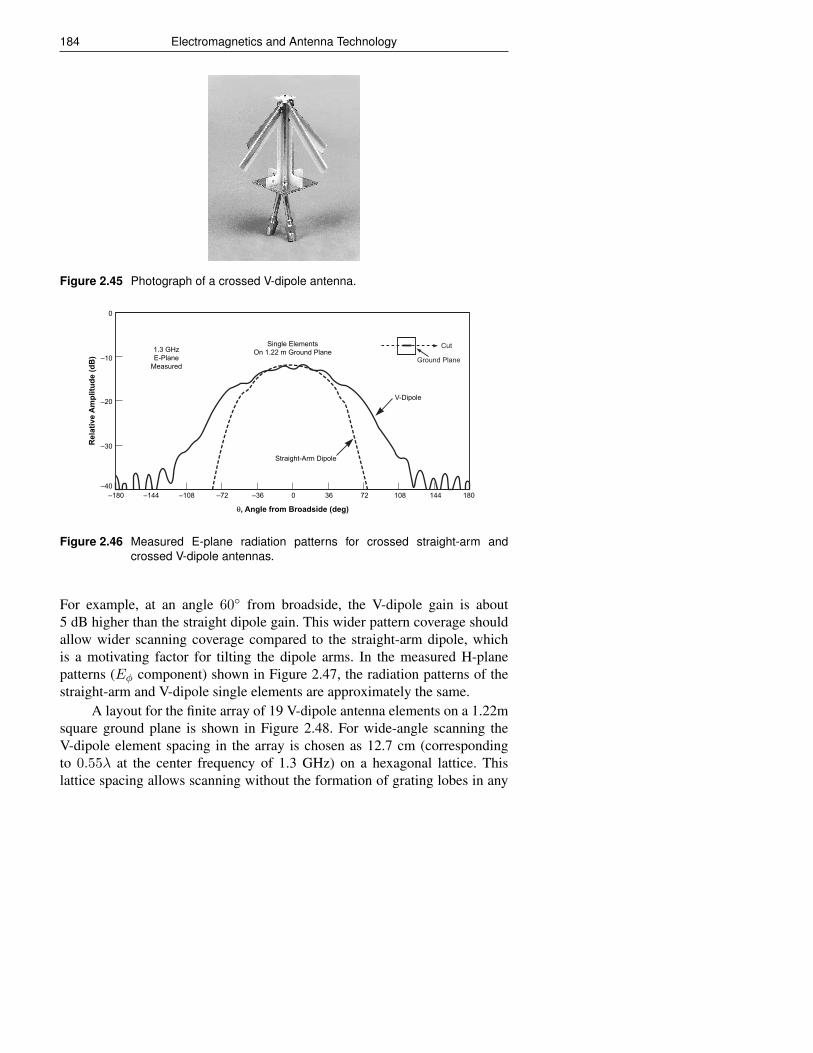
184 Electromagnetics and Antenna Technology
Figure 2.45 Photograph of a crossed V-dipole antenna.
1.3 GHzE-Plane
Measured
Single ElementsOn 1.22 m Ground Plane
Straight-Arm Dipole
V-Dipole
0
–10
–20
–30
–40–180 –144 –108 –72 –36 0 36 72 108 144 180
θ, Angle from Broadside (deg)
Rel
ativ
e A
mp
litu
de
(dB
)
430822_m_6.ai
Ground Plane
Cut
Figure 2.46 Measured E-plane radiation patterns for crossed straight-arm andcrossed V-dipole antennas.
For example, at an angle 60 from broadside, the V-dipole gain is about5 dB higher than the straight dipole gain. This wider pattern coverage shouldallow wider scanning coverage compared to the straight-arm dipole, whichis a motivating factor for tilting the dipole arms. In the measured H-planepatterns (Eφ component) shown in Figure 2.47, the radiation patterns of thestraight-arm and V-dipole single elements are approximately the same.
A layout for the finite array of 19 V-dipole antenna elements on a 1.22msquare ground plane is shown in Figure 2.48. For wide-angle scanning theV-dipole element spacing in the array is chosen as 12.7 cm (correspondingto 0.55λ at the center frequency of 1.3 GHz) on a hexagonal lattice. Thislattice spacing allows scanning without the formation of grating lobes in any
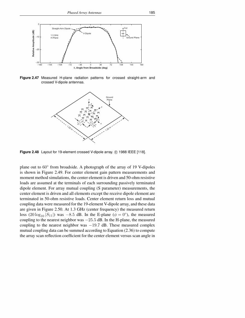
Phased Array Antennas 185
0
–10
–20
–30–180 –144 –108 –72 –36 0
θ, Angle from Broadside (deg)
Rel
ativ
e A
mp
litu
de
(dB
)
36 72 108 144 180
V-Dipole
Ground Plane
CutStraight-Arm Dipole
1.3 GHzH-Plane
430822_m_7.ai
Figure 2.47 Measured H-plane radiation patterns for crossed straight-arm andcrossed V-dipole antennas.
1.22 m
11.0 cm
1.22 m
12.7 cm
z
y
GroundPlane
x
430822_m_8.ai
θ
φ
Figure 2.48 Layout for 19-element crossed V-dipole array. c© 1988 IEEE [118].
plane out to 60 from broadside. A photograph of the array of 19 V-dipolesis shown in Figure 2.49. For center element gain pattern measurements andmoment method simulations, the center element is driven and 50-ohm resistiveloads are assumed at the terminals of each surrounding passively terminateddipole element. For array mutual coupling (S parameter) measurements, thecenter element is driven and all elements except the receive dipole element areterminated in 50-ohm resistive loads. Center element return loss and mutualcoupling data were measured for the 19-element V-dipole array, and these dataare given in Figure 2.50. At 1.3 GHz (center frequency) the measured returnloss (20 log10 |S11|) was −8.5 dB. In the E-plane (φ = 0), the measuredcoupling to the nearest neighbor was −25.5 dB. In the H-plane, the measuredcoupling to the nearest neighbor was −19.7 dB. These measured complexmutual coupling data can be summed according to Equation (2.36) to computethe array scan reflection coefficient for the center element versus scan angle in
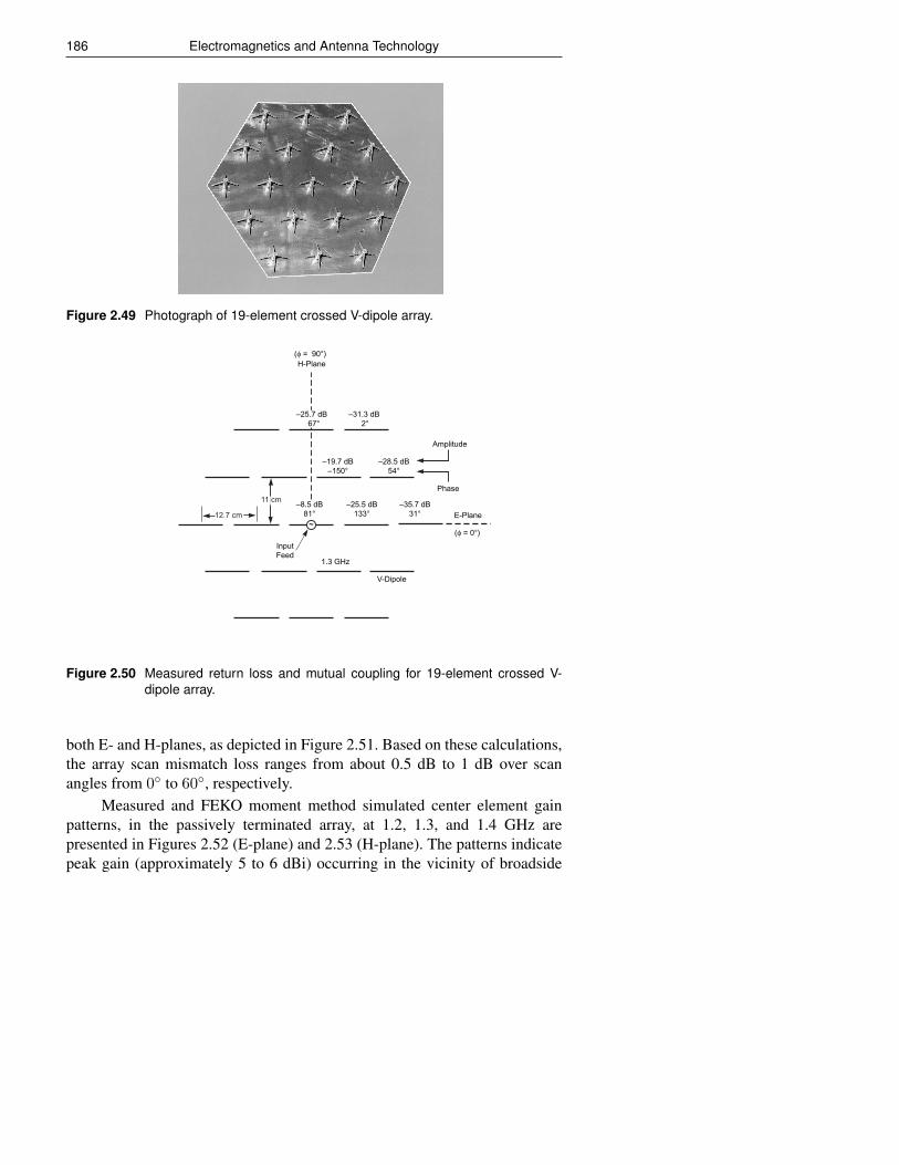
186 Electromagnetics and Antenna Technology
Figure 2.49 Photograph of 19-element crossed V-dipole array.
H-Plane
–31.3 dB 2°
–19.7 dB–150°
–28.5 dB54°
–8.5 dB81°
–25.5 dB133°
–35.7 dB31° E-Plane
(φ = 0°)
(φ = 90°)
InputFeed
Amplitude
Phase
~
–25.7 dB 67°
1.3 GHz
V-Dipole
430822_m_10.ai
11 cm
12.7 cm
Figure 2.50 Measured return loss and mutual coupling for 19-element crossed V-dipole array.
both E- and H-planes, as depicted in Figure 2.51. Based on these calculations,the array scan mismatch loss ranges from about 0.5 dB to 1 dB over scanangles from 0 to 60, respectively.
Measured and FEKO moment method simulated center element gainpatterns, in the passively terminated array, at 1.2, 1.3, and 1.4 GHz arepresented in Figures 2.52 (E-plane) and 2.53 (H-plane). The patterns indicatepeak gain (approximately 5 to 6 dBi) occurring in the vicinity of broadside
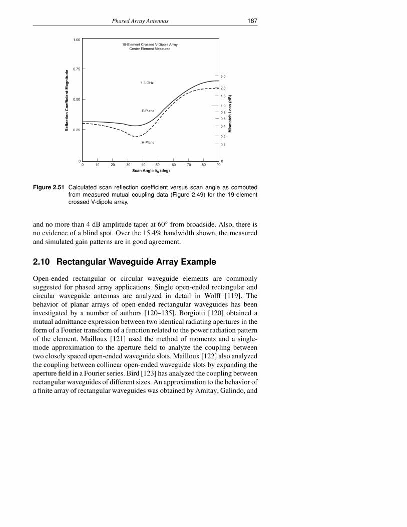
Phased Array Antennas 187
19-Element Crossed V-Dipole ArrayCenter Element Measured
1.00
0.75
0.50
0.25
00 10 20 30 40 50 60 70 80 90
Scan Angle θs (deg)
Ref
lect
ion
Co
effi
cien
t M
agn
itu
de
3.0
2.0
1.5
1.0
0.8
0.6
0.4
0.2
0.1
0
1.3 GHz
E-Plane
H-Plane
Mis
mat
ch L
oss
(d
B)
430822_m_11.aiFigure 2.51 Calculated scan reflection coefficient versus scan angle as computed
from measured mutual coupling data (Figure 2.49) for the 19-elementcrossed V-dipole array.
and no more than 4 dB amplitude taper at 60 from broadside. Also, there isno evidence of a blind spot. Over the 15.4% bandwidth shown, the measuredand simulated gain patterns are in good agreement.
2.10 Rectangular Waveguide Array Example
Open-ended rectangular or circular waveguide elements are commonlysuggested for phased array applications. Single open-ended rectangular andcircular waveguide antennas are analyzed in detail in Wolff [119]. Thebehavior of planar arrays of open-ended rectangular waveguides has beeninvestigated by a number of authors [120–135]. Borgiotti [120] obtained amutual admittance expression between two identical radiating apertures in theform of a Fourier transform of a function related to the power radiation patternof the element. Mailloux [121] used the method of moments and a single-mode approximation to the aperture field to analyze the coupling betweentwo closely spaced open-ended waveguide slots. Mailloux [122] also analyzedthe coupling between collinear open-ended waveguide slots by expanding theaperture field in a Fourier series. Bird [123] has analyzed the coupling betweenrectangular waveguides of different sizes. An approximation to the behavior ofa finite array of rectangular waveguides was obtained by Amitay, Galindo, and

188 Electromagnetics and Antenna Technology
10
0
–10
–20
–30–90 –60 –30 0 30 60 90
Gai
n (d
Bi)
10
0
–10
–20
–30–90 –60 –30 0 30 60 90
Gai
n (d
Bi)
10
0
–10
–20
–30–90 –60 –30 0 30 60 90
Gai
n (d
Bi)
MeasuredSimulated
MeasuredSimulated
MeasuredSimulated
1.2 GHz= 0°
Feeding xz DipoleE-Plane
(Center Element)
θ (deg)
1.3 GHz= 0°
Feeding xz DipoleE-Plane
(Center Element)
1.4 GHz= 0°
Feeding xz DipoleE-Plane
(Center Element)
(a)
(b)
(c)
φ
φ
φ
Figure 2.52 Measured and moment method simulated center element gain patternsfor 19-element V-dipole array. Feeding xz dipole, E-plane, φ = 0 cut. (a)1.2 GHz, (b) 1.3 GHz, and (c) 1.4 GHz.
Wu [6] by using infinite array techniques with finite array excitation. Wu alsoanalyzed a finite array of parallel plate waveguides [124] Cha and Hsiao [125]and Hidayet [126] investigated the reflection coefficients of planar waveguidearrays of size up to 13× 13 for a rectangular grid. Hidayet also analyzeda 7× 7 planar array arranged in triangular grid. Luzwick and Harrington[127] investigated the coupled power between elements of 7× 7 rectangularand triangular grid arrays. Wang [128] investigated the measured E-planeradiation patterns for the center element of a 3× 41 array of rectangularwaveguides and performed an infinite array analysis of both rectangular andridged waveguide arrays.
Consider now an example 7-element linear array of rectangular waveg-uide elements, which is analyzed by the FEKO method of moments solver.
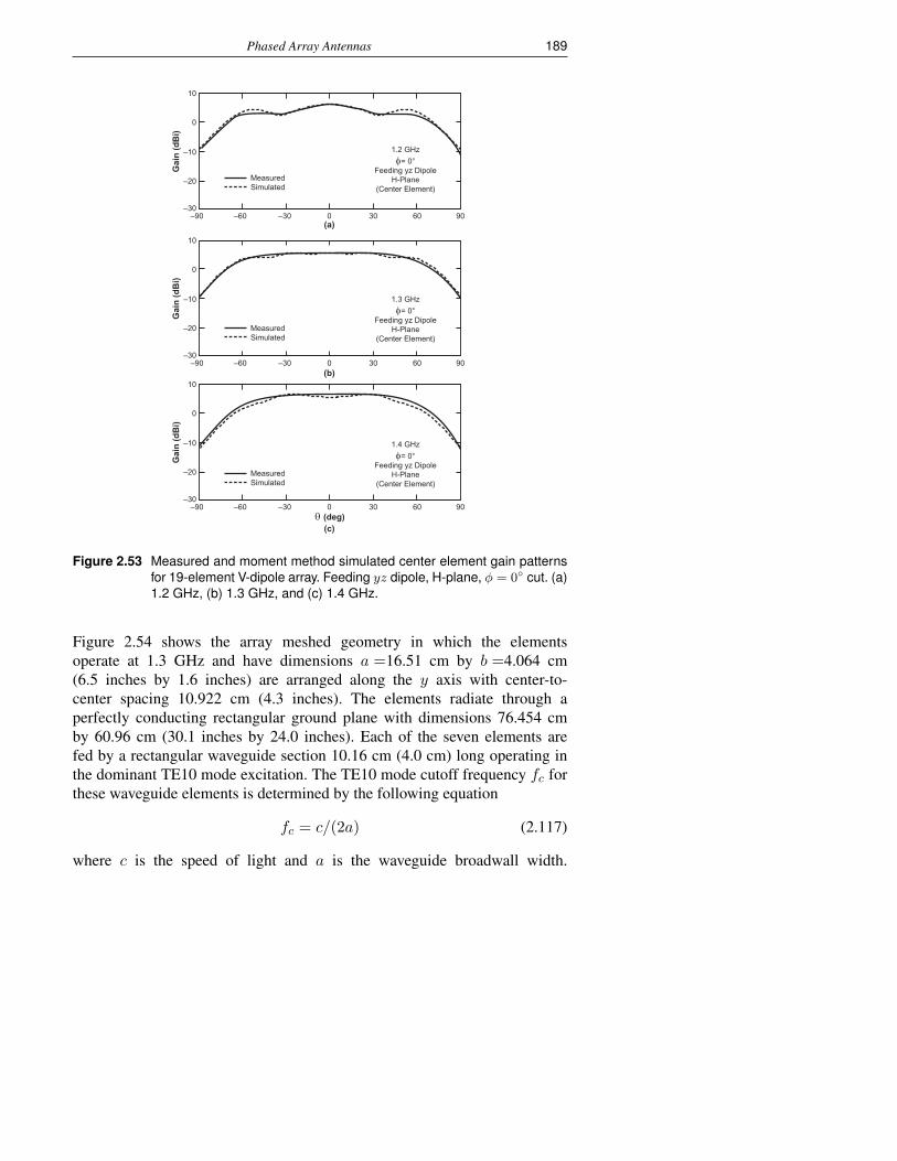
Phased Array Antennas 189
10
0
–10
–20
–30–90 –60 –30 0 30 60 90
Gai
n (d
Bi)
10
0
–10
–20
–30–90 –60 –30 0 30 60 90
Gai
n (d
Bi)
10
0
–10
–20
–30–90 –60 –30 0 30 60 90
Gai
n (d
Bi)
MeasuredSimulated
MeasuredSimulated
MeasuredSimulated
1.2 GHzφ= 0°
Feeding yz DipoleH-Plane
(Center Element)
θ (deg)
1.3 GHzφ= 0°
Feeding yz DipoleH-Plane
(Center Element)
1.4 GHzφ= 0°
Feeding yz DipoleH-Plane
(Center Element)
(a)
(b)
(c)
Figure 2.53 Measured and moment method simulated center element gain patternsfor 19-element V-dipole array. Feeding yz dipole, H-plane, φ = 0 cut. (a)1.2 GHz, (b) 1.3 GHz, and (c) 1.4 GHz.
Figure 2.54 shows the array meshed geometry in which the elementsoperate at 1.3 GHz and have dimensions a =16.51 cm by b =4.064 cm(6.5 inches by 1.6 inches) are arranged along the y axis with center-to-center spacing 10.922 cm (4.3 inches). The elements radiate through aperfectly conducting rectangular ground plane with dimensions 76.454 cmby 60.96 cm (30.1 inches by 24.0 inches). Each of the seven elements arefed by a rectangular waveguide section 10.16 cm (4.0 cm) long operating inthe dominant TE10 mode excitation. The TE10 mode cutoff frequency fc forthese waveguide elements is determined by the following equation
fc = c/(2a) (2.117)
where c is the speed of light and a is the waveguide broadwall width.
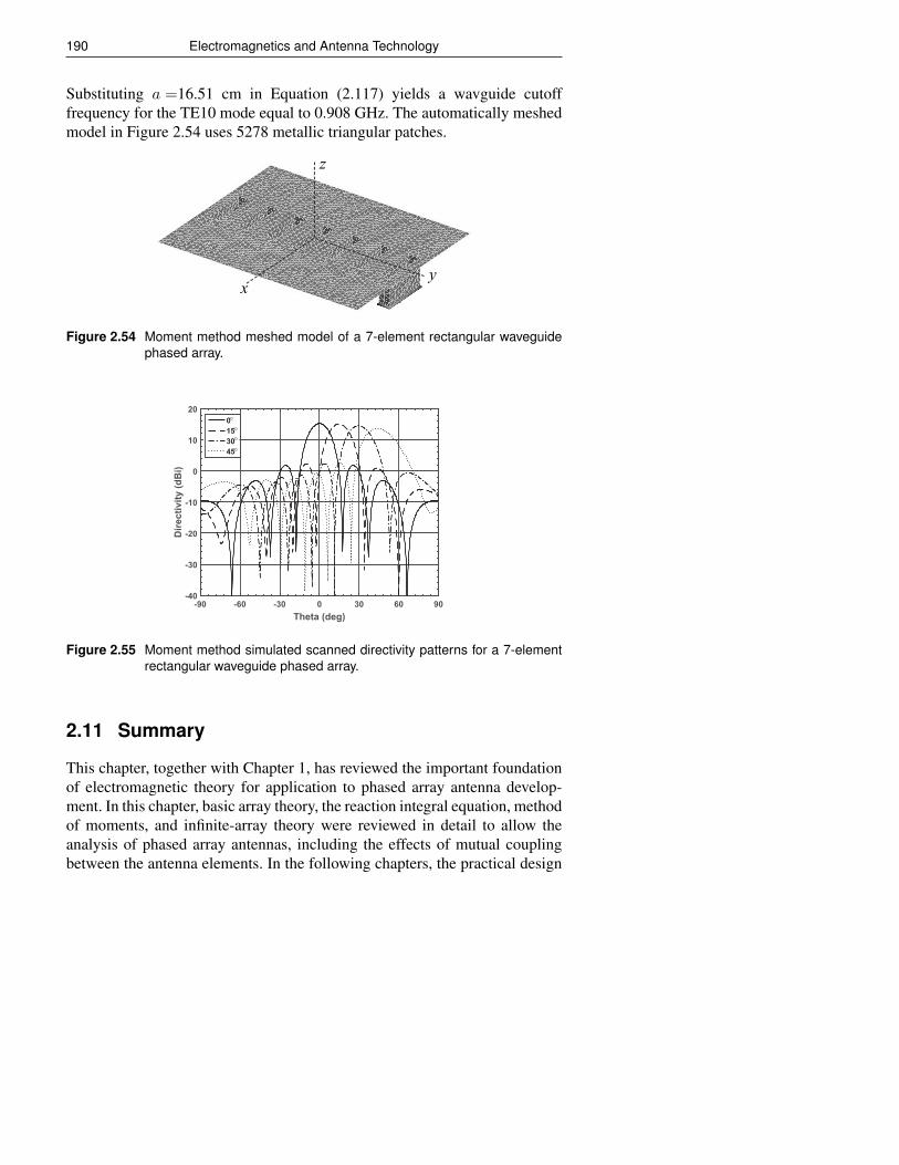
190 Electromagnetics and Antenna Technology
Substituting a =16.51 cm in Equation (2.117) yields a wavguide cutofffrequency for the TE10 mode equal to 0.908 GHz. The automatically meshedmodel in Figure 2.54 uses 5278 metallic triangular patches.
x
z
y
Figure 2.54 Moment method meshed model of a 7-element rectangular waveguidephased array.
-90 -60 -30 0 30 60 90Theta (deg)
-40
-30
-20
-10
0
10
20
Dire
ctiv
ity (d
Bi)
0153045
°°°°
Figure 2.55 Moment method simulated scanned directivity patterns for a 7-elementrectangular waveguide phased array.
2.11 Summary
This chapter, together with Chapter 1, has reviewed the important foundationof electromagnetic theory for application to phased array antenna develop-ment. In this chapter, basic array theory, the reaction integral equation, methodof moments, and infinite-array theory were reviewed in detail to allow theanalysis of phased array antennas, including the effects of mutual couplingbetween the antenna elements. In the following chapters, the practical design

Phased Array Antennas 191
and development of ultrawideband array antennas is described. The methodof moments is used in designing and analyzing the performance of theseprototype antennas.
References[1] J.D. Kraus, Antennas. New York: McGraw-Hill, 1950.
[2] S.A. Schelkunoff and H.T. Friis, Antennas: Theory and Practice. New York: Wiley,1952.
[3] W.L. Stutzman and G.A. Thiele, Antenna Theory and Design, 2nd ed. New York: Wiley,1998.
[4] J. Volakis, ed., Antenna Engineering Handbook, 4th ed. New York: McGraw-Hill, 2007.
[5] C.A. Balanis, Antenna Theory and Design, 3rd ed. New York: Wiley, 2005.
[6] N. Amitay, V. Galindo, and C.P. Wu, Theory and Analysis of Phased Array Antennas.New York: Wiley, 1972, ch. 1.
[7] A.A. Oliner and G.H. Knittel, eds., Phased Array Antennas. Dedham, Mass.: ArtechHouse, 1972.
[8] R.C. Hansen, ed., Significant Phased Array Papers. Dedham, Mass.: Artech House,1973.
[9] R.J. Mailloux, Phased Array Handbook, 2nd ed. Norwood, Mass.: Artech House, 2005.
[10] E. Brookner, ed., Practical Phased-Array Antenna Systems. Norwood, Mass.: ArtechHouse, 1991.
[11] R.C. Hansen, Microwave Scanning Antennas, vol. II: Array Theory and Practice. LosAltos, Calif.: Peninsula Publishing, 1985.
[12] R.C. Hansen, Phased Array Antennas, 2nd ed. New York: Wiley, 2009.
[13] A.K. Bhattacharyya, Phased Array Antennas. New York: Wiley, 2006.
[14] T. Jeffrey, Phased-Array Radar Design: Application of Radar Fundamentals. Raleigh,North Carolina: Scitech Pub Inc., 2009.
[15] A.J. Fenn, Adaptive Antennas and Phased Arrays for Radar and Communications.Norwood, Mass.: Artech House, 2008.
[16] D.R. Billetter, Multifunction Array Radar. Norwood, Mass.: Artech House, 1989.
[17] S.P. Skobelev, Phased Array Antennas with Optimized Element Patterns. Norwood,Mass.: Artech House, 2011.
[18] H.J. Visser, Array and Phased Array Antenna Basics. New York: Wiley, 2005.
[19] R.L. Haupt, Antenna Arrays: A Computational Approach. New York: Wiley-IEEE Press,2010.

192 Electromagnetics and Antenna Technology
[20] D. Ehyale, Novel Approaches to the Design of Phased Array Antennas: Low Cost, LowComplexity Phased Array Antenna Design. LAP Lambert Academic Publishing, 2012.
[21] E. Brookner, “Phased-Array Radars,” Scientific American, vol. 252, no. 2, 1985, pp. 94–102.
[22] A.J. Fenn, D.H. Temme, W.P. Delaney, and W.E. Courtney, “The Development ofPhased Array Radar Technology,” Lincoln Laboratory Journal, vol. 12, no. 2, 2000,pp. 321–340.
[23] J.L. Allen, L. Cartledge, W.P. Delaney, and J. Dibartolo, et al., “Phased Array RadarStudies, 1 July 1959 to 1 July 1960,” Technical Report 228, MIT Lincoln Laboratory,12 Aug. 1960, DTIC no. AD-0249470.
[24] J.L. Allen, L. Cartledge, W.P. Delaney, and J. Dibartolo, “Phased Array Radar Studies,1 July 1960 to 1 July 1961,” Technical Report 236, MIT Lincoln Laboratory, 13 Nov.1961, DTIC no. AD-271724.
[25] J.L. Allen, D.M. Bernella, W.W. Carpenter, and W.P. Delaney, “Phased Array RadarStudies, 1 July 1961 to 1 July 1963,” Technical Report 299, MIT Lincoln Laboratory,20 Feb. 1963, DTIC no. AD-417572.
[26] J.L. Allen, D.M. Bernella, F. Betts, and L. Cartledge, “Phased Array Radar Studies, 1July 1963 to 1 July 1964,” Technical Report 381, MIT Lincoln Laboratory, 31 March1965, DTIC no. AD-629363.
[27] J.L. Allen, “A Theoretical Limitation on the Formation of Lossless Multiple Beams inLinear Arrays," IRE Trans. Antennas and Propagation, vol. 9, no. 4, 1961, pp. 350–352.
[28] W.P. Delaney, “An RF Multiple Beam Forming Technique," Group Report 41G-0012,Lincoln Laboratory, 9 Aug. 1961, DTIC no. AD-262017.
[29] J.L. Allen, “Theory of Array Antennas (with Emphasis on Radar Applications),”Technical Report 323, Lincoln Laboratory, 25 July 1963, DTIC no. AD-422945.
[30] B.L. Diamond, “A Generalized Approach to the Analysis of Infinite Planar PhasedArray Antennas,” Proc. IEEE, vol. 56, no. 11, 1968, pp. 1837–1851.
[31] B.L. Diamond and G.H. Knittel, “A New Procedure for the Design of a WaveguideElement for a Phased-Array Antenna,” in Phased Array Antennas, A.A. Oliner and G.H.Knittel, eds. Dedham, Mass.: Artech House, 1972, pp. 149–156.
[32] J.L. Allen, “Gain and Impedance Variation in Scanned Dipole Arrays,” IRE Trans.Antennas and Propagation, vol. 10, no. 5, 1962, pp. 566–572.
[33] J.L. Allen, “On Surface-Wave Coupling Between Elements of Large Arrays,” IEEETrans. Antennas and Propagation, vol. 13, no. 4, 1965, pp. 638–639.
[34] J.L. Allen and B.L. Diamond, “Mutual Coupling in Array Antennas,” Technical Report424, Lincoln Laboratory, 4 Oct. 1966, DTIC no. AD-648153.
[35] B.L. Diamond, “Small Arrays – Their Analysis and Their Use for the Design of ArrayElements,” in Phased Array Antennas, A.A. Oliner and G.H. Knittel, eds. Dedham,Mass.: Artech House, 1972, pp. 127–131.

Phased Array Antennas 193
[36] A.J. Fenn, “Theoretical and Experimental Study of Monopole Phased Array Antennas,”IEEE Trans. Antennas and Propagation, vol. 34, no. 10, 1985, pp. 1118–1126.
[37] J. Butler, and R. Lowe, “Beam-Forming Matrix Simplifies Design of ElectronicallyScanned Antennas," Electron. Des., vol. 9, 12 Apr. 1961, pp. 170–173.
[38] R.J. Mailloux, “Phased Array Theory and Technology,” Proc. IEEE, vol. 70, no. 3, 1982,pp. 246–291.
[39] G.N. Tsandoulas, “Unidimensionally Scanned Phased Arrays,” IEEE Trans. Antennasand Propagation, vol. 28, no. 1, 1980, pp. 86–99.
[40] G.N. Tsandoulas, “Wideband Limitations of Waveguide Arrays,” Microwave J., vol. 15,no. 9, 1972, pp. 49–56.
[41] G.N. Tsandoulas and G.H. Knittel, “The Analysis and Design of Dual-PolarizationSquare-Waveguide Phased Arrays,” IEEE Trans. Antennas and Propagation, vol. 21,no. 6, 1973, pp. 796–808.
[42] G.H. Knittel, “Relation of Radar Range Resolution and Signal-to-Noise Ratio toPhased-Array Bandwidth, ” IEEE Trans. Antennas and Propagation, vol. 22, no. 3,1974, pp. 418–426.
[43] E. Brookner, ed. Radar Technology. Norwood, Mass.: Artech House, 1991.
[44] G.W. Stimson, Introduction to Airborne Radar. Raleigh, North Carolina: ScitechPublishing, 1998, pp. 546–562.
[45] E.J. Kelly and G.N. Tsandoulas, “A Displaced Phase Center Antenna Concept for SpaceBased Radar Applications,” IEEE Eascon, Sept. 1983, pp. 141–148.
[46] G.N. Tsandoulas, “Space-Based Radar,” Science, 17 July 1987, pp. 257–262.
[47] M.I. Skolnik, ed., Radar Handbook, 3rd ed. New York: McGraw-Hill, 2008.
[48] H.K. Schuman, D.R. Pflug, and L.D. Thompson, “Infinite Planar Arrays of ArbitrarilyBent Thin Wire Radiators,” IEEE Trans. Antennas Propagation, vol. 32, no. 3, 1984,pp. 364–377.
[49] E.D. Sharp, “A Triangular Arrangement of Planar-Array Elements That Reduces theNumber Needed,” IRE Trans. Antennas and Propagation, vol. 9, no. 2, 1961, pp. 126–129.
[50] N.R. Brennecke and W.N. Moule, “Uses of Fences to Optimize Operating Impedanceof Phased Arrays Using an Improved Measuring Technique,” IEEE Antennas andPropagation Soc. Int. Symp. Dig., 1964, pp. 134–142.
[51] B.A. Munk, Frequency Selective Surfaces: Theory and Design. New York: Wiley, 2000.
[52] B.A. Munk, Finite Antenna Arrays and FSS. New York: Wiley, 2003.
[53] A.J. Fenn and P.T. Hurst, Ultrawideband Phased Array Antenna Technology for Sensingand Communications Systems, MIT Lincoln Laboratory Book Series, Cambridge, MA:The MIT Press, 2015.
[54] K.F. Braun, Electrical Oscillations and Wireless Telegraphy, Nobel Prize Lecture, 11

194 Electromagnetics and Antenna Technology
Dec. 1909.
[55] R.J. Mailloux, “A History of Phased Array Antennas," Chapter 17 in History of Wireless,T.K. Sarkar, R.J. Mailloux, A.A. Oliner, M. Salazar-Palma, and D.L. Sengupta, eds.New Jersey: Wiley, 2006.
[56] W. Delaney, “From Vision to Reality: 50+ Years of Phased Array Development," 2016IEEE Int. Symp. on Phased Array Systems and Technology.
[57] E. Brookner, “Developments and Breakthroughs in Radars and Phased-Arrays," 2016IEEE Radar Conference.
[58] J.S. Herd and M.D. Conway, “The Evolution to Modern Phased Array Architectures,"Proc. IEEE vol. 104, no. 3, March 2016, pp. 519–529.
[59] M. Dudek, I. Nasr; G. Bozsik; M. Hamouda; D. Kissinger; G. Fischer, “System Analysisof a Phased-Array Radar Applying Adaptive Beam-Control for Future AutomotiveSafety Applications," IEEE Transactions on Vehicular Technology, vol. 64, no. 1, 2015,pp. 34 – 47.
[60] G.M. Rebeiz; S.-Y. Kim; O. Inac; W. Shin; O. Gurbuz; Y.-C. Ou; F. Golcuk; T. Kanar;B.-H. Ku, “Millimeter-Wave Large-Scale Phased-Arrays for 5G Systems," 2015 IEEEMTT-S International Microwave Symposium, 2015, pp. 1–3.
[61] M.H. Novak, F.A. Miranda, John L. Volakis, “An Ultra-Wideband Millimeter-WavePhased Array," 2016 10th European Conference on Antennas and Propagation(EuCAP), 2016 pp. 1 – 3.
[62] M. Agiwal; A. Roy; N. Saxena, “Next Generation 5G Wireless Networks: AComprehensive Survey," IEEE Communications Surveys & Tutorials vol. 18, no. 3,2016, pp. 1617 – 1655.
[63] P.W. Howells, “Explorations in Fixed and Adaptive Resolution at GE and SURC,” IEEETrans. Antennas and Propagation, vol. 24, no. 5, 1976, pp. 575–584.
[64] S.P. Applebaum, “Adaptive Arrays,” IEEE Trans. Antennas and Propagation, vol. 24,no. 5, 1976, pp. 585–598.
[65] W.F. Gabriel, “Adaptive Arrays – An Introduction,” Proc. IEEE, vol. 64, 1976, pp. 239–271.
[66] J.T. Mayhan, “Some Techniques for Evaluating the Bandwidth Characteristics ofAdaptive Nulling Systems,” IEEE Trans. Antennas and Propagation, vol. 27, no. 3,1979, pp. 363–373.
[67] J.T. Mayhan, A.J. Simmons, and W.C. Cummings, “Wide-Band Adaptive AntennaNulling Using Tapped Delay Lines,” IEEE Trans. Antennas and Propagation, vol. 29,no. 6, 1981, pp. 923–936.
[68] A.J. Fenn, “Evaluation of Adaptive Phased Array Far-Field Nulling Performance in theNear-Field Region,” IEEE Trans. Antennas and Propagation, vol. 38, no. 2, 1990, pp.173–185.
[69] R.A. Monzingo and T.W. Miller, Introduction to Adaptive Arrays. New York: Wiley,1980.

Phased Array Antennas 195
[70] R.T. Compton, Jr., Adaptive Antennas, Concepts and Performance. Upper Saddle River,New Jersey: Prentice-Hall, 1988.
[71] M.M. Weiner, Adaptive Antennas and Receivers. Boca Raton, Florida: CRC Press, 2006.
[72] S. Chandran, ed., Adaptive Antenna Arrays: Trends and Applications. Berlin: Springer-Verlag, 2004.
[73] D.G. Manolakis, V.K. Ingle, and S.M. Kogon, Statistical and Adaptive SignalProcessing: Spectral Estimation, Signal Modeling, Adaptive Filtering, and ArrayProcessing. Norwood, Mass.: Artech House, 2005.
[74] R. Nitzberg, Adaptive Signal Processing for Radar. Norwood, Mass.: Artech House,1992.
[75] A. Farina, Antenna-Based Signal Processing Techniques for Radar Systems. Norwood,Mass.: Artech House, 1992.
[76] J.E. Hudson, Adaptive Array Principles. New York: Peter Peregrinus, 1981.
[77] A. J. Fenn; G. A. King, Experimental investigation of an adaptive feedback algorithmfor hot spot reduction in radio-frequency phased-array hyperthermia, IEEE Trans. onBiomedical Eng. 1996, vol. 43, no. 3, pp. 273 - 280.
[78] A.J. Fenn, Adaptive Phased Array Thermotherapy for Cancer, Boston, MA: Artech,2009.
[79] M. A. Jensen; J. W. Wallace, “A Review of Antennas and Propagation for MIMOWireless Communications," IEEE Trans. on Antennas and Propagation, vol. 52, no.11, 2004, pp. 2810 – 2824.
[80] F. C. Robey, S. Coutts, D. Weikle, J. C. McHarg and K. Cuomo, “MIMO radar theoryand experimental results," Conference Record of the Thirty-Eighth Asilomar Conferenceon Signals, Systems and Computers, 2004, vol. 1, 2004, pp. 300–304.
[81] Y.I. Abramovich, G.J. Frazer, B.A. Johnson, “Principles of Mode-Selective MIMOOTHR," IEEE Trans. on Aerospace and Electronic Systems, vol. 49, no. 3, 2013, pp.1839 - 1868,
[82] C.J. Wilson, Electronically Steerable Field Reflector Techniques, Technical Report No.RADC-TR-64-521, Feb. 1965.
[83] W.D. Fitzgerald, “Limited Electronic Scanning with an Offset-Feed Near-FieldGregorian System,” MIT Lincoln Laboratory Technical Report 486, 24 Sept. 1971.
[84] J.A. Martinez-Lorenzo, A. Garcia-Pino, B. Gonzalez-Valdes, and C.M. Rappaport,“Zooming and Scanning Gregorian Confocal Dual Reflector Antennas,” IEEE Trans.on Antennas and Propagat., vol. 56, no. 9, 2008, pp. 2910-2919.
[85] A.J. Fenn and R.J. Richardson, “Analysis of an Adaptive Two-Reflector Phased-ArrayFed System,” 1980 IEEE Antennas and Propagation Society International SymposiumDigest, 2-6 June 1980, pp. 134-137.
[86] Kelly, E.J., and G.N. Tsandoulas, “A Displaced Phase Center Antenna Concept forSpace Based Radar Applications,” IEEE Eascon, September 1983, pp. 141-148.

196 Electromagnetics and Antenna Technology
[87] Tsandoulas, G.N., “Space-Based Radar,” Science, Vol. 237, July 17, 1987, pp. 257-262.
[88] Fenn, A.J., “Analysis of Phase-Focused Near-Field Testing for Multiphase-CenterAdaptive Radar Systems,” IEEE Trans. Antennas Propagat., Vol. 40, No. 8, 1992,pp. 878-887.
[89] C. L. Dolph, “A Current Distribution for Broadside Arrays Which Optimizes theRelationship Between Beamwidth and Side Lobe Level," Proc. IRE, vol. 31, June 1946,pp. 335–318.
[90] D. Barbiere. “A Method for Calculating the Current Distribution of TschebyscheffArrays," Proc. IRE, vol. 10, January 1952, pp. 78-82.
[91] A. D. Bresler, “A New Algorithm for Calculating the Current Distributions of Dolph-Chebyshev Arrays," IEEE Trans. Antennas Propagat., vol. AP-28, no. 6, November1980, pp. 951,952.
[92] T.T. Taylor, “Design of Circular Apertures for Narrow Beamwidth and Low SideLobes," IEEE Trans. on Antennas and Propagat., vol AP-8, no. 4, January 1960, pp.17–22.
[93] R.L. Thomas, A Practical Introduction to Impedance Matching. Dedham, Mass: ArtechHouse, 1976.
[94] A.E.H. Love, “The Integration of the Equations of Propagation of Electric Waves,"Philosophical Trans., Series A197, 1901, pp. 1-45.
[95] S.A. Schelkunoff, “On Diffraction and Radiation of Electromagnetic Waves," Phys.Rev., vol. 56, 1939, pp. 308–316.
[96] R.F. Harrington, Time-Harmonic Electromagnetic Fields, New York: McGraw-Hill,1961.
[97] J.R. Mautz and R.F. Harrington, “Electromagnetic Scattering from a HomogeneousMaterial Body of Revolution," Int. J. Electronics and Communications (AEU), vol. 33,1979, pp. 71-80.
[98] E. Arvas, A.Rahhal-Arabi, A. Sadigh, S.M. Rao, “Scattering from Multiple Conductingand Dielectric Bodies of Arbitrary Shape," IEEE Antennas and Propagat. Magazine,vol. 33, no. 2, 1991, pp. 29-36.
[99] U. Jakobus, “Comparison of Different Techniques for the Treatment of LossyDielectric/Magnetic Bodies within the Method of Moments Formulation," Int. J.Electronics and Communications (AEU), vol. 54, no. 3, 2000, pp. 163-173.
[100] C.A. Balanis, Advanced Engineering Electromagnetics, 2nd ed. New Jersey: Wiley,2012.
[101] V.H. Rumsey, “Reaction Concept in Electromagnetic Theory," Physical Review, vol. 94,1954, pp. 1483–1491.
[102] R.F. Harrington, Field Computation by Moment Methods. New York: Macmillan, 1968.
[103] S. Rao, D. Wilton, and A. Glisson, “Electromagnetic Scattering by Surfaces of Arbitrary

Phased Array Antennas 197
Shape," IEEE Trans. Antennas and Propagation, vol. 30, no. 5, 1982, pp. 409–418.
[104] E.H. Newman and K. Kingsley, “An Introduction to the Method of Moments," ComputerPhysics Communications, vol. 68, 1991, pp. 1–18.
[105] J.H. Richmond and N.H. Geary, “Mutual Impedance of Nonplanar-Skew SinusoidalDipoles,” IEEE Trans. Antennas and Propagation, vol. 23, no. 3, 1975, pp. 412–414.
[106] J.H. Richmond, “Radiation and Scattering by Thin-Wire Structures in a HomogeneousConducting Medium (Computer Program Desc.),” IEEE Trans. Antennas andPropagation, vol. 22, no. 2, 1974, p. 365.
[107] K.E. Schmidt, “Mutual Impedance of Nonplanar Skew Dipoles," IEEE Trans. Antennasand Propagation, vol. 44, no. 9, 1996, pp. 1298–1299.
[108] N.N. Wang, “Reaction Formulation for Radiation and Scattering from Plates, CornerReflectors, and Dielectric-Coated Cylinders," The Ohio State University, Project Report2902-15, Columbus, Ohio, Apr. 1974.
[109] W.C. Gibson, The Method of Moments in Electromagnetics. Boca Raton, Florida:Chapman & Hall, 2008.
[110] W.C. Chew, J.M. Jin, E. Michielssen, and J. Song, Fast and Efficient Algorithms inComputational Electromagnetics. Norwood, Mass.: Artech House, 2001.
[111] H. Jingjian, Z. Xiaofa, X Shaoyi,W. Weiwei, and Y. Naichang, “Suppression of Cross-Polarization of the Microstrip Integrated Balun-Fed Printed Dipole Antenna,” Int. J. ofAntennas and Propagation, Volume 2014, pp. 1–8.
[112] B. Edward and D. Rees, “A Broadband Printed Dipole with Integrated Balun,”Microwave J., vol. 30, no. 5, pp. 339–344, 1987.
[113] R. L. Li, T. Wu, B. Pan, K. Lim, J. Laskar, and M. M. Tentzeris, “Equivalent-CircuitAnalysis of a Broadband Printed Dipole with Adjusted Integrated Balun and an Arrayfor Base Station Applications,” IEEE Trans. on Antennas and Propagat., vol. 57, no. 7,2009, pp. 2180–2184.
[114] P. Lindberg, E. Ojefors, Z. Barna, A. Thornell-Pers, and A. Rydberg,“Dual WidebandPrinted Dipole Antenna with Integrated Balun,” IET Microwaves, Antennas &Propagation, vol. 1, no. 3, 2007, pp. 707–711.
[115] M. Scott, “A Printed Dipole for Wide-Scanning Array Application,” Proc. 11th Int.Conf. on Antenna and Propagation, Manchester, UK, vol. 1, no. 480, 2001, pp. 37–40.
[116] H.-R. Chuang and L.-C. Kuo,“3-D FDTD Design Analysis of a 2.4-GHz Polarization-Diversity Printed Dipole Antenna with Integrated Balun and Polarization-SwitchingCircuit for WLAN and Wireless Communication Applications,” IEEE Transactions onMicrowave Theory and Techniques, vol. 51, no. 2, 2003, pp. 374–381.
[117] Mayer, E.D., and A. Hessel, “Feed Region Modes in Dipole Phased Arrays,” IEEETrans. Antennas Propagat., Vol. 30, No. 1, 1982, pp. 66-75.
[118] Fenn, A.J., “Element Gain Pattern Prediction for Finite Arrays of V-Dipole Antennasover Ground Plane,” IEEE Trans. Antennas Propagat., Vol. 36, No. 11, 1988, pp. 1629-1633.

198 Electromagnetics and Antenna Technology
[119] E.A. Wolff, Antenna Analysis, New York: John Wiley, pp.192-208.
[120] G.V. Borgiotti, “A Novel Expression for the Mutual Admittance of Planar RadiatingElements,” IEEE Trans. Antennas Propagat., Vol. 16, No. 3, 1968, pp. 329-333.
[121] R.J. Mailloux, “First-Order Solutions for Mutual Coupling Between Waveguides WhichPropagate Two Orthogonal Modes,” IEEE Trans. Antennas Propagat., Vol. 17, No. 6,1969, pp. 740-746.
[122] R.J. Mailloux, “Radiation and Near-Field Coupling Between Two Collinear Open-Ended Waveguides,” IEEE Trans. Antennas Propagat., Vol. 17, No. 1, 1969, pp. 49-55.
[123] T.S. Bird, “Analysis of Mutual Coupling in Finite Arrays of Different-Sized RectangularWaveguides,” IEEE Trans. Antennas Propagat., Vol. 38, No. 2, 1990, pp. 166–172.
[124] C.P. Wu, “Analysis of Finite Parallel-Plate Waveguide Arrays,” IEEE Trans. AntennasPropagat., Vol. 18, No. 3, 1970, pp. 328–334.
[125] A.G. Cha and J.K. Hsiao, “A Matrix Formulation for Large Scale NumericalComputation of the Finite Planar Waveguide Array Problem,” IEEE Trans. AntennasPropagat., Vol. AP-22, No. 1, January 1974, pp. 106–108.
[126] M.A. Hidayet, “Finite Phased Array Analysis,” Ph.D. dissertation, Univ. Michigan,1974.
[127] J. Luzwick and R.F. Harrington, “Mutual Coupling Analysis in a Finite PlanarRectangular Waveguide Antenna Array,” Dept. Elect. Computer Eng., Syracuse Univ.,Tech. Rep., No. 7, June 1978.
[128] S.S. Wang, “Wide-Angle Wide-Band Elements for Phased Arrays,” Ph.D. dissertation,Polytechnic Institute of New York, 1975.
[129] J.D. Kraus, Antennas, New York: McGraw-Hill, 1950, ch. 4.
[130] R.F. Harrington and J.R. Mautz, “A Generalized Network Formulation for ApertureProblems,” Sci.Rep. no. 8 contract F19628-73-C-0047, A.F. Cambridge Res. Lab., Rep.AFCRL-TR-75-0589, November 1975.
[131] A.J. Fenn, “Moment Method Calculation of Reflection Coefficient for WaveguideElements in a Finite Planar Phased Antenna Array,” Ph.D. dissertation, The Ohio StateUniv., 1978.
[132] A. J. Fenn, G.A. Thiele, and B.A. Munk, “Moment Method Analysis of FiniteRectangular Waveguide Phased Arrays,” IEEE Trans. Antennas Propagat., Vol. 30, No.4, 1982, pp. 554–564.
[133] B.L. Diamond, “Resonance Phenomena in Waveguide Arrays,” IEEE G-AP Int. Symp.Dig., 1967, pp. 110–115.
[134] H. Yavuz and O.M. Buyukdura, “Mutual Coupling Effects of Finite Rectangular PhasedArrays,” IEEE Antennas and Propagat. Soc. Int. Symp. Digest, 1994, pp. 418–421.
[135] P. Grassi, R. Mittra, A. Monorchio, and G. Manara, “Characterization of FiniteWaveguide Arrays Using a New Generalized Scattering Matrix Approach,” IEEEAntennas and Propagat. Symposium Digest, 2004, pp. 125–128.

Phased Array Antennas 199
[136] A. Pellegrini, A. Monorchio, G. Manara, R. Mittra, “A Hybrid Mode Matching-FiniteElement Method and Spectral Decomposition Approach for the Analysis of Large FinitePhased Arrays of Waveguides", IEEE Trans. on Antennas and Propagat., vol. 62, 2014,pp. 2553–2561.

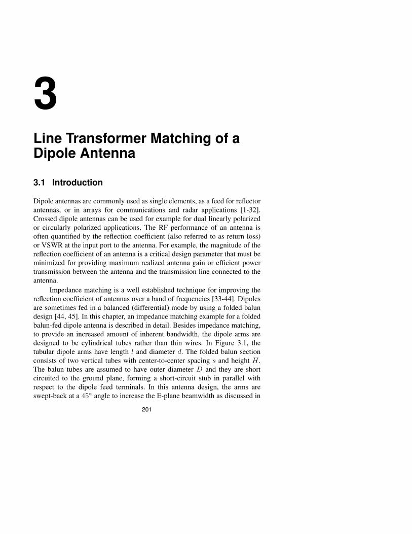
3Line Transformer Matching of aDipole Antenna
3.1 Introduction
Dipole antennas are commonly used as single elements, as a feed for reflectorantennas, or in arrays for communications and radar applications [1-32].Crossed dipole antennas can be used for example for dual linearly polarizedor circularly polarized applications. The RF performance of an antenna isoften quantified by the reflection coefficient (also referred to as return loss)or VSWR at the input port to the antenna. For example, the magnitude of thereflection coefficient of an antenna is a critical design parameter that must beminimized for providing maximum realized antenna gain or efficient powertransmission between the antenna and the transmission line connected to theantenna.
Impedance matching is a well established technique for improving thereflection coefficient of antennas over a band of frequencies [33-44]. Dipolesare sometimes fed in a balanced (differential) mode by using a folded balundesign [44, 45]. In this chapter, an impedance matching example for a foldedbalun-fed dipole antenna is described in detail. Besides impedance matching,to provide an increased amount of inherent bandwidth, the dipole arms aredesigned to be cylindrical tubes rather than thin wires. In Figure 3.1, thetubular dipole arms have length l and diameter d. The folded balun sectionconsists of two vertical tubes with center-to-center spacing s and height H .The balun tubes are assumed to have outer diameter D and they are shortcircuited to the ground plane, forming a short-circuit stub in parallel withrespect to the dipole feed terminals. In this antenna design, the arms areswept-back at a 45 angle to increase the E-plane beamwidth as discussed in
201
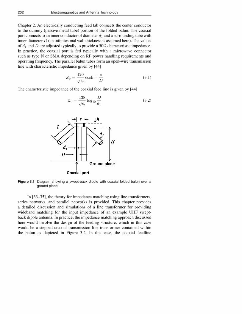
202 Electromagnetics and Antenna Technology
Chapter 2. An electrically conducting feed tab connects the center conductorto the dummy (passive metal tube) portion of the folded balun. The coaxialport connects to an inner conductor of diameter d1 and a surrounding tube withinner diameterD (an infinitesimal wall thickness is assumed here). The valuesof d1 and D are adjusted typically to provide a 50Ω characteristic impedance.In practice, the coaxial port is fed typically with a microwave connectorsuch as type N or SMA depending on RF power handling requirements andoperating frequency. The parallel balun tubes form an open-wire transmissionline with characteristic impedance given by [44]
Zo =120√εr
cosh−1 s
D(3.1)
The characteristic impedance of the coaxial feed line is given by [44]
Zo =138√εr
log10D
d1(3.2)
Figure 3.1 Diagram showing a swept-back dipole with coaxial folded balun over aground plane.
In [33–35], the theory for impedance matching using line transformers,series networks, and parallel networks is provided. This chapter providesa detailed discussion and simulations of a line transformer for providingwideband matching for the input impedance of an example UHF swept-back dipole antenna. In practice, the impedance matching approach discussedhere would involve the design of the feeding structure, which in this casewould be a stepped coaxial transmission line transformer contained withinthe balun as depicted in Figure 3.2. In this case, the coaxial feedline

Line Transformer Matching of a Dipole Antenna 203
contains an impedance transformer section with an inner conductor withdiameter d2 adjusted for a desired characteristic impedance to match theinput impedance of the dipole. Chapter 1 reviewed transmission line theoryin detail. The next section (Section 3.2) provides a brief review as it relatesto the derivation of the line transformer matching theory (Section 3.3). Anapplication of the line transformer matching theory to designing a widebandswept-back dipole is described along with simulated moment method resultsin Section 3.4. Section 3.5 describes a comparison between simulated andmeasured mismatch loss results for a prototype swept-back dipole. Section 3.6simulates the radiation patterns for the wideband swept-back dipole feeding aparabolic reflector antenna. Section 3.7 has a summary.
Figure 3.2 Diagram showing a swept-back dipole with line transformer section with acoaxial folded balun over a ground plane.
3.2 Basic Transmission Line Theory
In this section, a brief review of basic transmission line theory is provided as itrelates to the line transformer impedance matching theory [33-35]. Referringto Figure 3.3, consider first a length l of transmission line with a characteristicimpedance Zo. Assume that the transmission line’s attenuation constant αis equal to zero. The electrical length is given by the quantity βl, whereβ = 2π/λ is the wavelength-dependent phase propagation constant of thetransmission line. Assume that an antenna has a complex load impedancedenoted as ZL. At a distance l along a lossless transmission line withcharacteristic impedance Zo and phase propagation constant β, the input
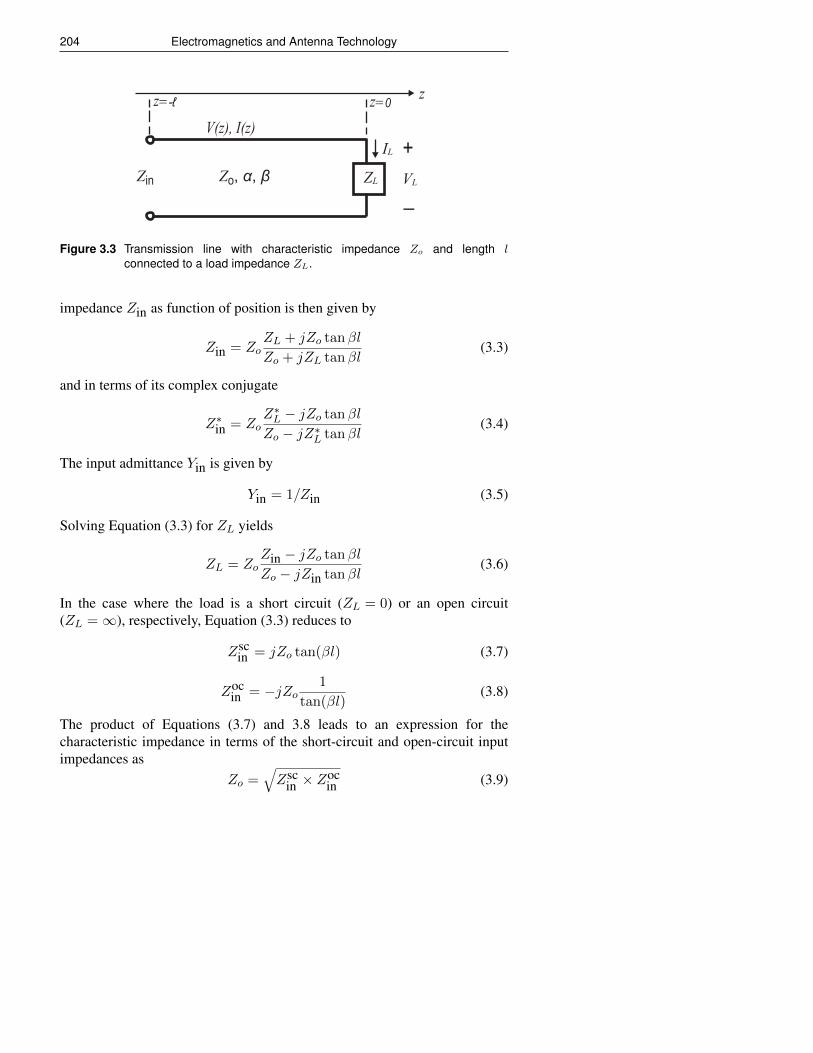
204 Electromagnetics and Antenna Technology
Zo, α, β ZL
V(z), I(z)z=-ℓ
VL
IL +
_
zz=0
Zin
Figure 3.3 Transmission line with characteristic impedance Zo and length lconnected to a load impedance ZL.
impedance Zin as function of position is then given by
Zin = ZoZL + jZo tanβl
Zo + jZL tanβl(3.3)
and in terms of its complex conjugate
Z∗in = ZoZ∗L − jZo tanβl
Zo − jZ∗L tanβl(3.4)
The input admittance Yin is given by
Yin = 1/Zin (3.5)
Solving Equation (3.3) for ZL yields
ZL = ZoZin − jZo tanβl
Zo − jZin tanβl(3.6)
In the case where the load is a short circuit (ZL = 0) or an open circuit(ZL =∞), respectively, Equation (3.3) reduces to
Zscin = jZo tan(βl) (3.7)
Zocin = −jZo
1
tan(βl)(3.8)
The product of Equations (3.7) and 3.8 leads to an expression for thecharacteristic impedance in terms of the short-circuit and open-circuit inputimpedances as
Zo =√Zsc
in × Zocin (3.9)
Line Transformer Matching of a Dipole Antenna 205
The reflection coefficient in terms of the load impedance ZL andtransmission line characteristic impedance Zo is given by
Γ =ZL − ZoZL + Zo
(3.10)
and in normalized form in terms of zL = ZL/Zo as
Γ =zL − 1
zL + 1= |Γ|ejφ (3.11)
It follows from Equation (3.11) that the normalized load impedance isexpressed as
zL =1 + Γ
1− Γ(3.12)
Rearranging Equation (3.10), the load impedance in terms of the reflectioncoefficient is given by
ZL = Zo1 + Γ
1− Γ(3.13)
The voltage standing wave ratio (VSWR) is expressed as
VSWR =1 + |Γ|1− |Γ|
(3.14)
Having reviewed some of the fundamental equations that quantify the inputimpedance, load impedance, reflection coefficient, and VSWR, the nextsection addresses line transformer impedance matching theory.
3.3 Line Transformer Impedance Matching Theory
In the impedance matching procedure that follows, electromagnetic simula-tions (or measurements) would be used to determine the input impedanceat the antenna terminals of the swept-back crossed dipole antenna depictedin Figure 3.1. The dipole arms and geometry and height of feed terminalswith respect to the ground plane are designed based on simple theoryand using prior experience, which is discussed later in this chapter. Inthe electromagnetic field simulations and line transformer calculations thatfollow, the dipole antenna is fed initially (before matching) with a standardZo = 50Ω coaxial feedline, which is not expected to provide the desiredfinal reflection coefficient magitude or VSWR. A voltage source is locatedat the input port of the 50-ohm coaxial feedline (located at the groundplane), and the input impedance of the antenna simulated at the ground plane
206 Electromagnetics and Antenna Technology
reference position is determined. (Note: the same approach can be appliedfor measurements). The next step is to transform the input impedance atthe ground plane to the complex load ZL at the antenna terminals usingEquation (3.6). This antenna terminal input impedance (load impedance)becomes the starting value for impedance matching. Next, a series transformertransmission line with derived values of characteristic impedance and lengthis introduced to improve the reflection coefficient. The input impedancematching technique discussed in this chapter is as follows:
• Plot the antenna load impedance (input impedance) in Cartesiancoordinates, where the horizontal axis is resistance and the verticalaxis is reactance,• Define a target maximum allowed VSWR (plotted as a circle) at an
input port located on a standard 50-ohm transmission line,• Draw an outer boundary circle (OBC) encompassing the input
impedance data at the antenna terminals and tangent to the targetVSWR circle,• Compute the required characteristic impedance of the line trans-
former Z ′o using the square root (geometric mean) of the productof the resistance minimum (denoted ROBC
min and resistance maximumROBC
max on the resistance axis intersecting the OBC, that is,
Z ′o =√ROBC
min ×ROBCmax (3.15)
• Compute and plot the family of transformation circles that ensuresimpedance values versus frequency will transform to within thedesired target VSWR (target circle).• Select a critical frequency in this case where the antenna load
impedance intersects the outer boundary circle, and locate thecorresponding transformation circle that encompasses the impedancedata point at this frequency, From the electrical length βl of thecorresponding transformation circle, solve for the transformer criticallength l = lc using β = 2π/λwhere λ is the wavelength at the criticalfrequency.• Tabulate the electrical line length of the transformer section over
the frequency band of interest, and verify that the input impedanceat the terminals of the dipole antenna tracks within the series oftransformation circles.• Transform the antenna load impedance to the input impedance
and reflection coefficient looking into the line transformer withcharacteristic impedance Z ′o and critical length lc.
Line Transformer Matching of a Dipole Antenna 207
• Normalize the reflection coefficient data to the final characteristicimpedance (50Ω) of the feedline attached to the transformer, and plotas the matched input impedance.
3.3.1 Target Circle for Maximum Allowed VSWR
Consider first a target circle, which is also referred to by some authors as adefinition circle [33-35]. The target circle defines the maximum allow VSWR,and is expressed mathematically and visually in the Cartesian compleximpedance coordinate system. Letting Zin = Rin + jXin, the equation for thetarget circle is given by
(Rin − a)2 +X2in = b2 (3.16)
where Rin is the input resistance, Xin is the input reactance, a is the offset ofthe center of the target circle from the value of zero input resistance, and b isthe radius of the circle. The a and b parameters are expressed in terms of thetarget transmission line characteristic impedance Zo and the VSWR as
a =Zo2
(VSWR +
1
VSWR
)(3.17)
b =Zo2
(VSWR− 1
VSWR
)(3.18)
and note thata2 − b2 = Zo (3.19)
Equation (3.16) is now expanded as
R2in − 2aRin +X2
in = b2 (3.20)
Noting for an arbitrary impedance Z that
Z = R+ jX (3.21)
Z∗ = R− jX (3.22)
andZ + Z∗ = 2R (3.23)
Z − Z∗ = j2X (3.24)
it follows thatZZ∗ = R2 +X2 (3.25)
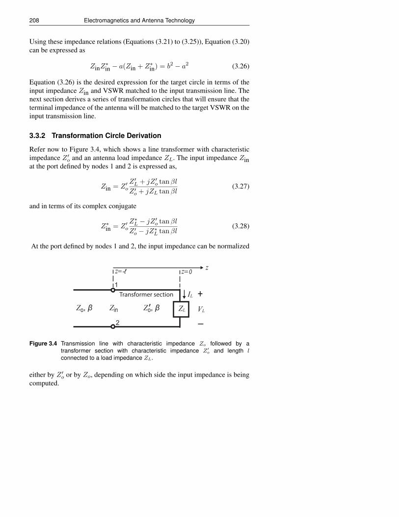
208 Electromagnetics and Antenna Technology
Using these impedance relations (Equations (3.21) to (3.25)), Equation (3.20)can be expressed as
ZinZ∗in − a(Zin + Z∗in) = b2 − a2 (3.26)
Equation (3.26) is the desired expression for the target circle in terms of theinput impedance Zin and VSWR matched to the input transmission line. Thenext section derives a series of transformation circles that will ensure that theterminal impedance of the antenna will be matched to the target VSWR on theinput transmission line.
3.3.2 Transformation Circle Derivation
Refer now to Figure 3.4, which shows a line transformer with characteristicimpedance Z ′o and an antenna load impedance ZL. The input impedance Zinat the port defined by nodes 1 and 2 is expressed as,
Zin = Z ′oZ ′L + jZ ′o tanβl
Z ′o + jZL tanβl(3.27)
and in terms of its complex conjugate
Z∗in = Z ′oZ∗L − jZ ′o tanβl
Z ′o − jZ∗L tanβl(3.28)
At the port defined by nodes 1 and 2, the input impedance can be normalized
Zo, β ZL
z=-ℓ
VL
IL +
_
zz=0
ZinZo, β ’
1
2
Transformer section
Figure 3.4 Transmission line with characteristic impedance Zo followed by atransformer section with characteristic impedance Z′o and length lconnected to a load impedance ZL.
either by Z ′o or by Zo, depending on which side the input impedance is beingcomputed.
Line Transformer Matching of a Dipole Antenna 209
Substituting Equations (3.27 and (3.28) into Equation (3.26) yields(Z ′o
ZL+jZ′o tanβlZ′o+jZL tanβl
) (Z ′o
Z∗L−jZ′o tanβl
Z′o−jZ∗L tanβl
)−a
[(Z ′o
ZL+jZ′o tanβlZ′o+jZL tanβl
)+(Z ′o
Z∗L−jZ′o tanβl
Z′o−jZ∗L tanβl
)]= b2 − a2 (3.29)
In the book by Reich [33], it is shown that Equation (3.29) can be expressedin the standard form of the equation of a circle center on the resistance axis atR and on the reactance axis at X with radius r as
(RL −R)2 + (XL −X)2 = r2 (3.30)
where
R =a(1 + tan2 βl)
1 + a2−b2(Z′o)
2 tan2 βl(3.31)
X =Zo tanβl
(a2−b2(Z′o)
2 − 1)
1 + a2−b2(Z′o)
2 tan2 βl(3.32)
r =b(1 + tan2 βl)
1 + a2−b2(Z′o)
2 tan2 βl(3.33)
Equation (3.30) is the desired transformation circle that forms a bilineartransformation to the target circle for a line transformer with characteristicimpedance Z ′o and electrical length βl. In other words, load impedance valuesZL that are located within the transformation circle will be transformedto impedance values within the desired target circle with characteristicimpedance Zo. To derive Equations (3.31) to (3.33) it is necessary first to mul-tiply all terms in Equation (3.29) by the expression (Z ′o + jZL tanβl)(Z ′o −jZ∗L tanβl). Next, the relations given by Equations (3.23) to (3.25 are used toexpress the equation in terms of RL and XL. Next, bring all terms involvingRL and XL to the left side and the remaining terms to the right side. Bycompleting the square for the RL and XL terms, and a considerable amountof algebraic manipulations, the desired results Equations (3.31) to (3.33) areobtained.
By referring to Equation (3.19) a further simplification of the transfor-mation Equations (3.31) to (3.33) is achieved, that is, replace a2 − b2 with Zo,so that
R =a(1 + tan2 βl)
1 + Zo(Z′o)
2 tan2 βl(3.34)
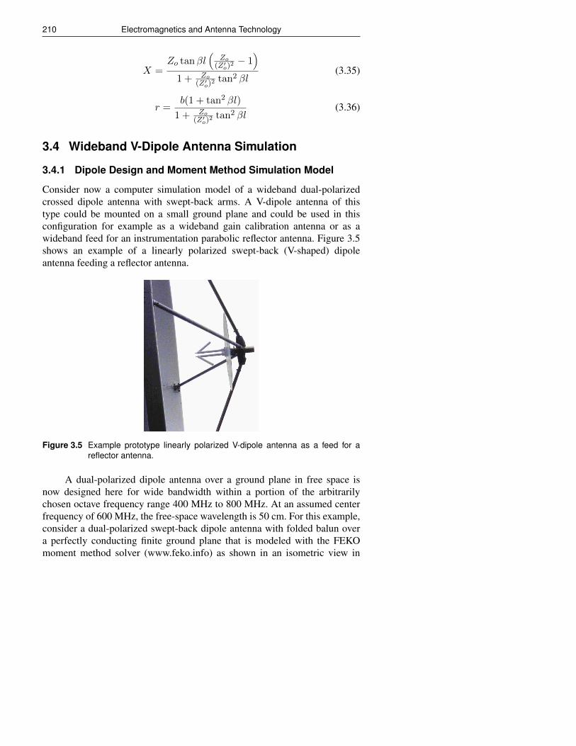
210 Electromagnetics and Antenna Technology
X =Zo tanβl
(Zo
(Z′o)2 − 1
)1 + Zo
(Z′o)2 tan2 βl
(3.35)
r =b(1 + tan2 βl)
1 + Zo(Z′o)
2 tan2 βl(3.36)
3.4 Wideband V-Dipole Antenna Simulation
3.4.1 Dipole Design and Moment Method Simulation Model
Consider now a computer simulation model of a wideband dual-polarizedcrossed dipole antenna with swept-back arms. A V-dipole antenna of thistype could be mounted on a small ground plane and could be used in thisconfiguration for example as a wideband gain calibration antenna or as awideband feed for an instrumentation parabolic reflector antenna. Figure 3.5shows an example of a linearly polarized swept-back (V-shaped) dipoleantenna feeding a reflector antenna.
Figure 3.5 Example prototype linearly polarized V-dipole antenna as a feed for areflector antenna.
A dual-polarized dipole antenna over a ground plane in free space isnow designed here for wide bandwidth within a portion of the arbitrarilychosen octave frequency range 400 MHz to 800 MHz. At an assumed centerfrequency of 600 MHz, the free-space wavelength is 50 cm. For this example,consider a dual-polarized swept-back dipole antenna with folded balun overa perfectly conducting finite ground plane that is modeled with the FEKOmoment method solver (www.feko.info) as shown in an isometric view in
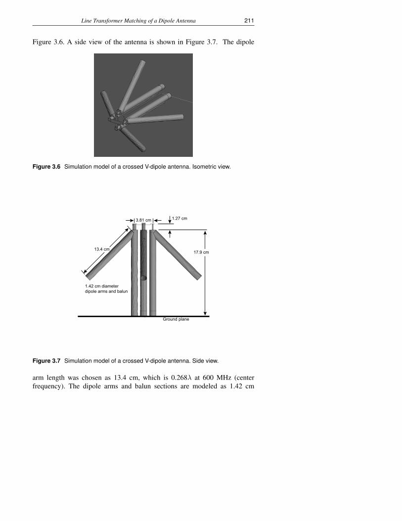
Line Transformer Matching of a Dipole Antenna 211
Figure 3.6. A side view of the antenna is shown in Figure 3.7. The dipole
Figure 3.6 Simulation model of a crossed V-dipole antenna. Isometric view.
Ground plane
17.9 cm13.4 cm
1.42 cm diameterdipole arms and balun
3.81 cm 1.27 cm
Figure 3.7 Simulation model of a crossed V-dipole antenna. Side view.
arm length was chosen as 13.4 cm, which is 0.268λ at 600 MHz (centerfrequency). The dipole arms and balun sections are modeled as 1.42 cm
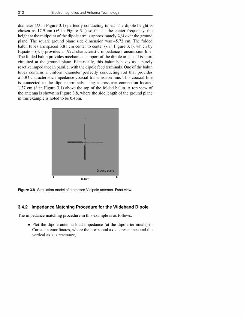
212 Electromagnetics and Antenna Technology
diameter (D in Figure 3.1) perfectly conducting tubes. The dipole height ischosen as 17.9 cm (H in Figure 3.1) so that at the center frequency, theheight at the midpoint of the dipole arm is approximately λ/4 over the groundplane. The square ground plane side dimension was 45.72 cm. The foldedbalun tubes are spaced 3.81 cm center to center (s in Figure 3.1), which byEquation (3.1) provides a 197Ω characteristic impedance transmission line.The folded balun provides mechanical support of the dipole arms and is shortcircuited at the ground plane. Electrically, this balun behaves as a purelyreactive impedance in parallel with the dipole feed terminals. One of the baluntubes contains a uniform diameter perfectly conducting rod that providesa 50Ω characteristic impedance coaxial transmission line. This coaxial lineis connected to the dipole terminals using a crossover connection located1.27 cm (h in Figure 3.1) above the top of the folded balun. A top view ofthe antenna is shown in Figure 3.8, where the side length of the ground planein this example is noted to be 0.46m.
0.46m
Ground plane
Figure 3.8 Simulation model of a crossed V-dipole antenna. Front view.
3.4.2 Impedance Matching Procedure for the Wideband Dipole
The impedance matching procedure in this example is as follows:
• Plot the dipole antenna load impedance (at the dipole terminals) inCartesian coordinates, where the horizontal axis is resistance and thevertical axis is reactance,
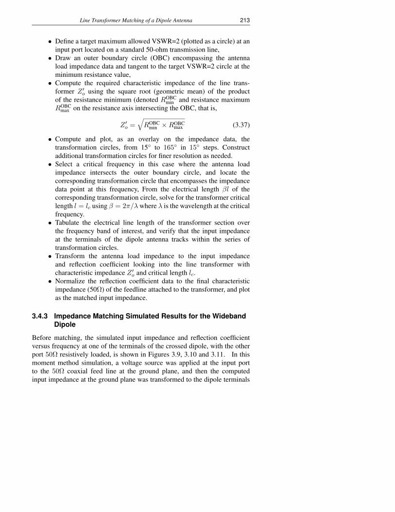
Line Transformer Matching of a Dipole Antenna 213
• Define a target maximum allowed VSWR=2 (plotted as a circle) at aninput port located on a standard 50-ohm transmission line,• Draw an outer boundary circle (OBC) encompassing the antenna
load impedance data and tangent to the target VSWR=2 circle at theminimum resistance value,• Compute the required characteristic impedance of the line trans-
former Z ′o using the square root (geometric mean) of the productof the resistance minimum (denoted ROBC
min and resistance maximumROBC
max on the resistance axis intersecting the OBC, that is,
Z ′o =√ROBC
min ×ROBCmax (3.37)
• Compute and plot, as an overlay on the impedance data, thetransformation circles, from 15 to 165 in 15 steps. Constructadditional transformation circles for finer resolution as needed.• Select a critical frequency in this case where the antenna load
impedance intersects the outer boundary circle, and locate thecorresponding transformation circle that encompasses the impedancedata point at this frequency, From the electrical length βl of thecorresponding transformation circle, solve for the transformer criticallength l = lc using β = 2π/λwhere λ is the wavelength at the criticalfrequency.• Tabulate the electrical line length of the transformer section over
the frequency band of interest, and verify that the input impedanceat the terminals of the dipole antenna tracks within the series oftransformation circles.• Transform the antenna load impedance to the input impedance
and reflection coefficient looking into the line transformer withcharacteristic impedance Z ′o and critical length lc.• Normalize the reflection coefficient data to the final characteristic
impedance (50Ω) of the feedline attached to the transformer, and plotas the matched input impedance.
3.4.3 Impedance Matching Simulated Results for the WidebandDipole
Before matching, the simulated input impedance and reflection coefficientversus frequency at one of the terminals of the crossed dipole, with the otherport 50Ω resistively loaded, is shown in Figures 3.9, 3.10 and 3.11. In thismoment method simulation, a voltage source was applied at the input portto the 50Ω coaxial feed line at the ground plane, and then the computedinput impedance at the ground plane was transformed to the dipole terminals
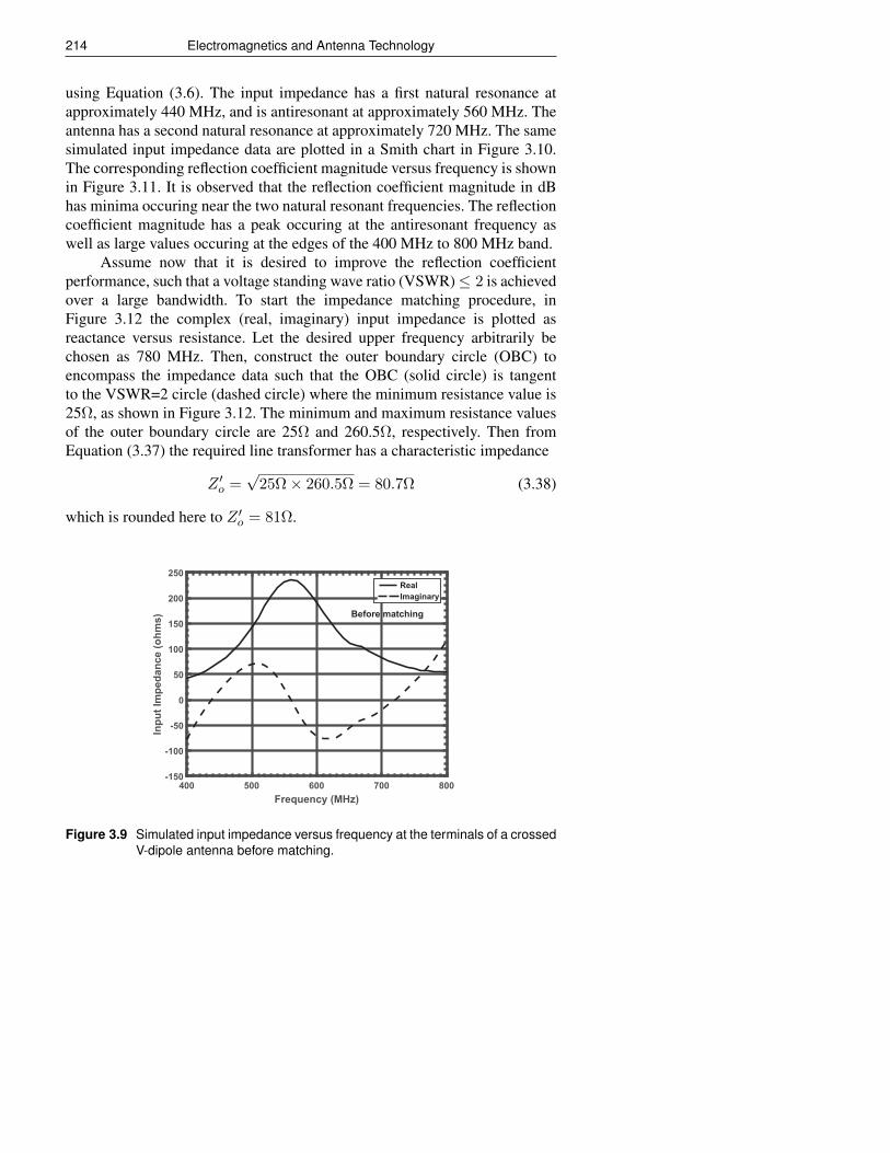
214 Electromagnetics and Antenna Technology
using Equation (3.6). The input impedance has a first natural resonance atapproximately 440 MHz, and is antiresonant at approximately 560 MHz. Theantenna has a second natural resonance at approximately 720 MHz. The samesimulated input impedance data are plotted in a Smith chart in Figure 3.10.The corresponding reflection coefficient magnitude versus frequency is shownin Figure 3.11. It is observed that the reflection coefficient magnitude in dBhas minima occuring near the two natural resonant frequencies. The reflectioncoefficient magnitude has a peak occuring at the antiresonant frequency aswell as large values occuring at the edges of the 400 MHz to 800 MHz band.
Assume now that it is desired to improve the reflection coefficientperformance, such that a voltage standing wave ratio (VSWR)≤ 2 is achievedover a large bandwidth. To start the impedance matching procedure, inFigure 3.12 the complex (real, imaginary) input impedance is plotted asreactance versus resistance. Let the desired upper frequency arbitrarily bechosen as 780 MHz. Then, construct the outer boundary circle (OBC) toencompass the impedance data such that the OBC (solid circle) is tangentto the VSWR=2 circle (dashed circle) where the minimum resistance value is25Ω, as shown in Figure 3.12. The minimum and maximum resistance valuesof the outer boundary circle are 25Ω and 260.5Ω, respectively. Then fromEquation (3.37) the required line transformer has a characteristic impedance
Z ′o =√
25Ω× 260.5Ω = 80.7Ω (3.38)
which is rounded here to Z ′o = 81Ω.
400 500 600 700 800Frequency (MHz)
-150
-100
-50
0
50
100
150
200
250
Inpu
t Im
peda
nce
(ohm
s) Before matching
RealImaginary
Figure 3.9 Simulated input impedance versus frequency at the terminals of a crossedV-dipole antenna before matching.
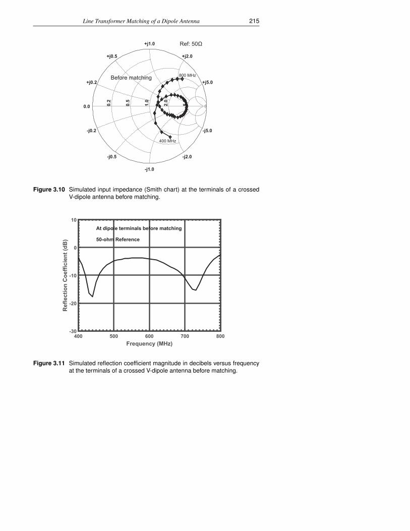
Line Transformer Matching of a Dipole Antenna 215
0.2
0.5
1.0
2.0
5.0
+j0.2
-j0.2
+j0.5
-j0.5
+j1.0
-j1.0
+j2.0
-j2.0
+j5.0
-j5.0
0.0
Before matching
400 MHz
800 MHz
Ref: 50Ω
Figure 3.10 Simulated input impedance (Smith chart) at the terminals of a crossedV-dipole antenna before matching.
400 500 600 700 800Frequency (MHz)
-30
-20
-10
0
10
Ref
lect
ion
Coe
ffici
ent (
dB)
At dipole terminals before matching
50-ohm Reference
Figure 3.11 Simulated reflection coefficient magnitude in decibels versus frequencyat the terminals of a crossed V-dipole antenna before matching.
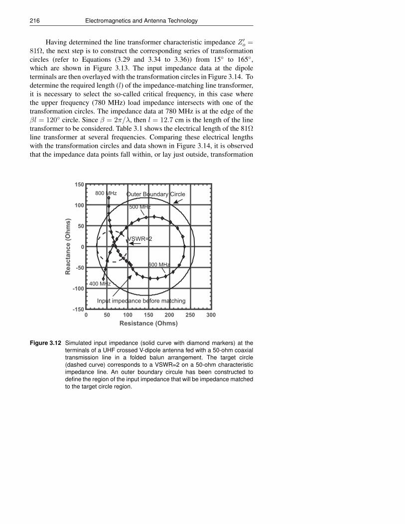
216 Electromagnetics and Antenna Technology
Having determined the line transformer characteristic impedance Z ′o =81Ω, the next step is to construct the corresponding series of transformationcircles (refer to Equations (3.29 and 3.34 to 3.36)) from 15 to 165,which are shown in Figure 3.13. The input impedance data at the dipoleterminals are then overlayed with the transformation circles in Figure 3.14. Todetermine the required length (l) of the impedance-matching line transformer,it is necessary to select the so-called critical frequency, in this case wherethe upper frequency (780 MHz) load impedance intersects with one of thetransformation circles. The impedance data at 780 MHz is at the edge of theβl = 120 circle. Since β = 2π/λ, then l = 12.7 cm is the length of the linetransformer to be considered. Table 3.1 shows the electrical length of the 81Ωline transformer at several frequencies. Comparing these electrical lengthswith the transformation circles and data shown in Figure 3.14, it is observedthat the impedance data points fall within, or lay just outside, transformation
0 50 100 150 200 250 300Resistance (Ohms)
-150
-100
-50
0
50
100
150
Rea
ctan
ce (O
hms)
Outer Boundary Circle
VSWR=2
Input impedance before matching
400 MHz
800 MHz
500 MHz
600 MHz
Figure 3.12 Simulated input impedance (solid curve with diamond markers) at theterminals of a UHF crossed V-dipole antenna fed with a 50-ohm coaxialtransmission line in a folded balun arrangement. The target circle(dashed curve) corresponds to a VSWR=2 on a 50-ohm characteristicimpedance line. An outer boundary circule has been constructed todefine the region of the input impedance that will be impedance matchedto the target circle region.
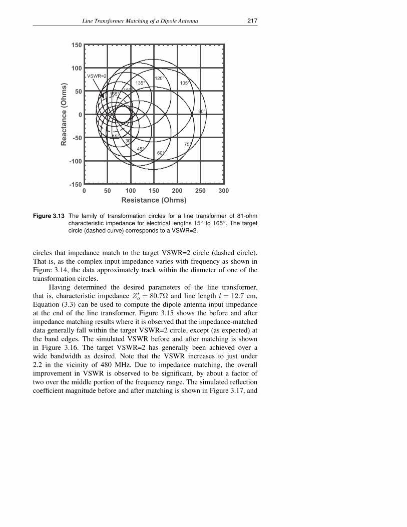
Line Transformer Matching of a Dipole Antenna 217
0 50 100 150 200 250 300Resistance (Ohms)
-150
-100
-50
0
50
100
150
Rea
ctan
ce (O
hms)
VSWR=2
30°
45°60°
75°
15°
165°
90°
105°120°
135°150°
Figure 3.13 The family of transformation circles for a line transformer of 81-ohmcharacteristic impedance for electrical lengths 15 to 165. The targetcircle (dashed curve) corresponds to a VSWR=2.
circles that impedance match to the target VSWR=2 circle (dashed circle).That is, as the complex input impedance varies with frequency as shown inFigure 3.14, the data approximately track within the diameter of one of thetransformation circles.
Having determined the desired parameters of the line transformer,that is, characteristic impedance Z ′o = 80.7Ω and line length l = 12.7 cm,Equation (3.3) can be used to compute the dipole antenna input impedanceat the end of the line transformer. Figure 3.15 shows the before and afterimpedance matching results where it is observed that the impedance-matcheddata generally fall within the target VSWR=2 circle, except (as expected) atthe band edges. The simulated VSWR before and after matching is shownin Figure 3.16. The target VSWR=2 has generally been achieved over awide bandwidth as desired. Note that the VSWR increases to just under2.2 in the vicinity of 480 MHz. Due to impedance matching, the overallimprovement in VSWR is observed to be significant, by about a factor oftwo over the middle portion of the frequency range. The simulated reflectioncoefficient magnitude before and after matching is shown in Figure 3.17, and

218 Electromagnetics and Antenna Technology
0 50 100 150 200 250 300Resistance (Ohms)
-150
-100
-50
0
50
100
150R
eact
ance
(Ohm
s)
165°
90°
105°120°
135°150°
30°
45°60°
75°
15°
400 MHz
800 MHz
600 MHz
500 MHz
550 MHz
650 MHz
780 MHz
700 MHz
450 MHz
Figure 3.14 Simulated input impedance (solid curve with diamond markers) atthe terminals of a UHF crossed V-dipole antenna fed with a 50-ohmcoaxial transmission line in a folded balun arrangement. The targetconstant VSWR=2 circle is shown as a dashed curve. The impedancetransformation circles from 15 to 165 are shown
the corresponding transmission mismatch loss is shown in Figure 3.18. Thetransmission mismatch loss before matching has a maximum value of about2.4 dB occuring near 560 MHz. After impedance matching the mismatch lossis less than about 0.6 dB from 420 MHz to 780 MHz – due to impedancematching the realized gain would be within 0.6 dB of the ideal antennadirectivity with no mismatch loss. For example, with the 81-ohm coaxial linetransformer section simulated in FEKO, at the center frequency of 600 MHzthe simulated boresight directivity of the swept-back dipole over ground planewas 6.45 dBi and the realized gain was 6.0 dBi – for this case the simulatedmismatch loss was 0.45 dB. Prior to matching with the line transformersection, for the constant 50-ohm coaxial feed at 600 MHz the simulatedboresight directivity was 6.45 dBi, but the realized gain was only 4.27 dBidue to the mismatch loss being 2.18 dB. Thus, with the line transformerdesign, at the center frequency the swept-back dipole realized gain increased
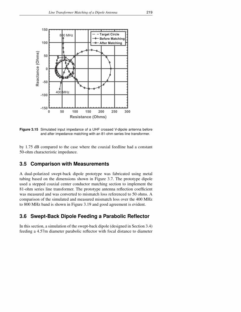
Line Transformer Matching of a Dipole Antenna 219
0 50 100 150 200 250 300Resistance (Ohms)
-150
-100
-50
0
50
100
150
Rea
ctan
ce (O
hms)
Target CircleBefore MatchingAfter Matching
400 MHz
800 MHz
Figure 3.15 Simulated input impedance of a UHF crossed V-dipole antenna beforeand after impedance matching with an 81-ohm series line transformer.
by 1.75 dB compared to the case where the coaxial feedline had a constant50-ohm characteristic impedance.
3.5 Comparison with Measurements
A dual-polarized swept-back dipole prototype was fabricated using metaltubing based on the dimensions shown in Figure 3.7. The prototype dipoleused a stepped coaxial center conductor matching section to implement the81-ohm series line transformer. The prototype antenna reflection coefficientwas measured and was converted to mismatch loss referenced to 50 ohms. Acomparison of the simulated and measured mismatch loss over the 400 MHzto 800 MHz band is shown in Figure 3.19 and good agreement is evident.
3.6 Swept-Back Dipole Feeding a Parabolic Reflector
In this section, a simulation of the swept-back dipole (designed in Section 3.4)feeding a 4.57m diameter parabolic reflector with focal distance to diameter
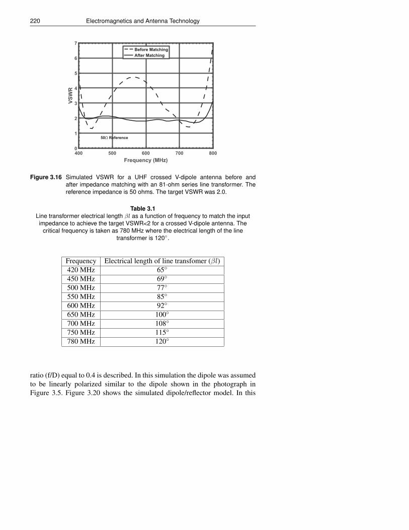
220 Electromagnetics and Antenna Technology
400 500 600 700 800Frequency (MHz)
0
1
2
3
4
5
6
7
VSW
R
Before MatchingAfter Matching
50Ω Reference
Figure 3.16 Simulated VSWR for a UHF crossed V-dipole antenna before andafter impedance matching with an 81-ohm series line transformer. Thereference impedance is 50 ohms. The target VSWR was 2.0.
Table 3.1Line transformer electrical length βl as a function of frequency to match the inputimpedance to achieve the target VSWR<2 for a crossed V-dipole antenna. The
critical frequency is taken as 780 MHz where the electrical length of the linetransformer is 120.
Frequency Electrical length of line transfomer (βl)420 MHz 65
450 MHz 69
500 MHz 77
550 MHz 85
600 MHz 92
650 MHz 100
700 MHz 108
750 MHz 115
780 MHz 120
ratio (f/D) equal to 0.4 is described. In this simulation the dipole was assumedto be linearly polarized similar to the dipole shown in the photograph inFigure 3.5. Figure 3.20 shows the simulated dipole/reflector model. In this
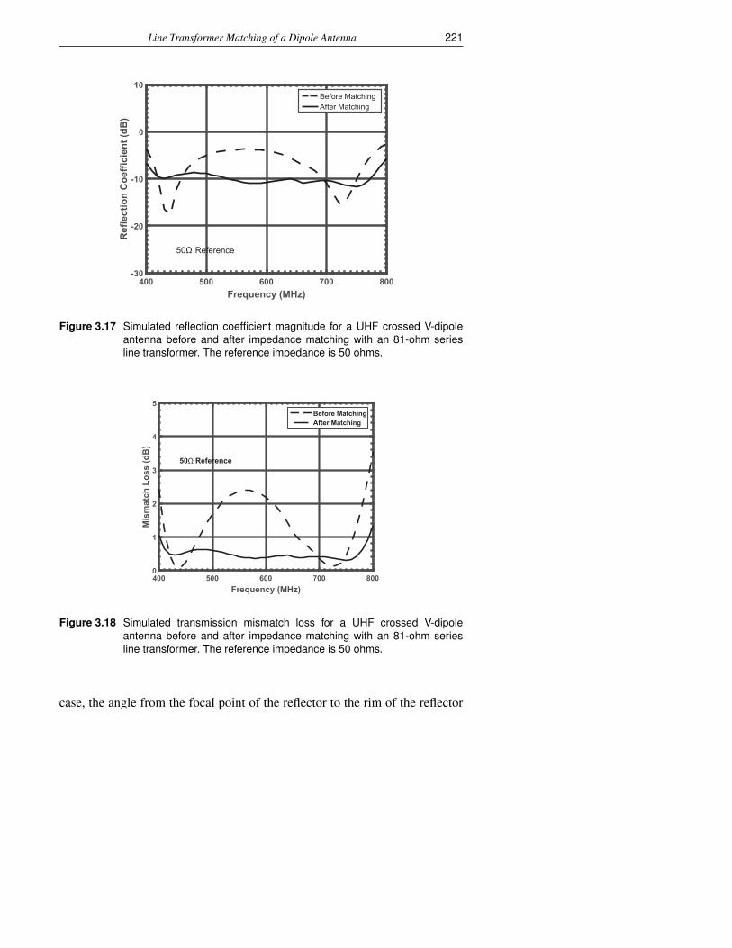
Line Transformer Matching of a Dipole Antenna 221
400 500 600 700 800Frequency (MHz)
-30
-20
-10
0
10
Ref
lect
ion
Coe
ffici
ent (
dB)
50Ω Reference
Before MatchingAfter Matching
Figure 3.17 Simulated reflection coefficient magnitude for a UHF crossed V-dipoleantenna before and after impedance matching with an 81-ohm seriesline transformer. The reference impedance is 50 ohms.
400 500 600 700 800Frequency (MHz)
0
1
2
3
4
5
Mis
mat
ch L
oss
(dB
)
50Ω Reference
Before MatchingAfter Matching
Figure 3.18 Simulated transmission mismatch loss for a UHF crossed V-dipoleantenna before and after impedance matching with an 81-ohm seriesline transformer. The reference impedance is 50 ohms.
case, the angle from the focal point of the reflector to the rim of the reflector
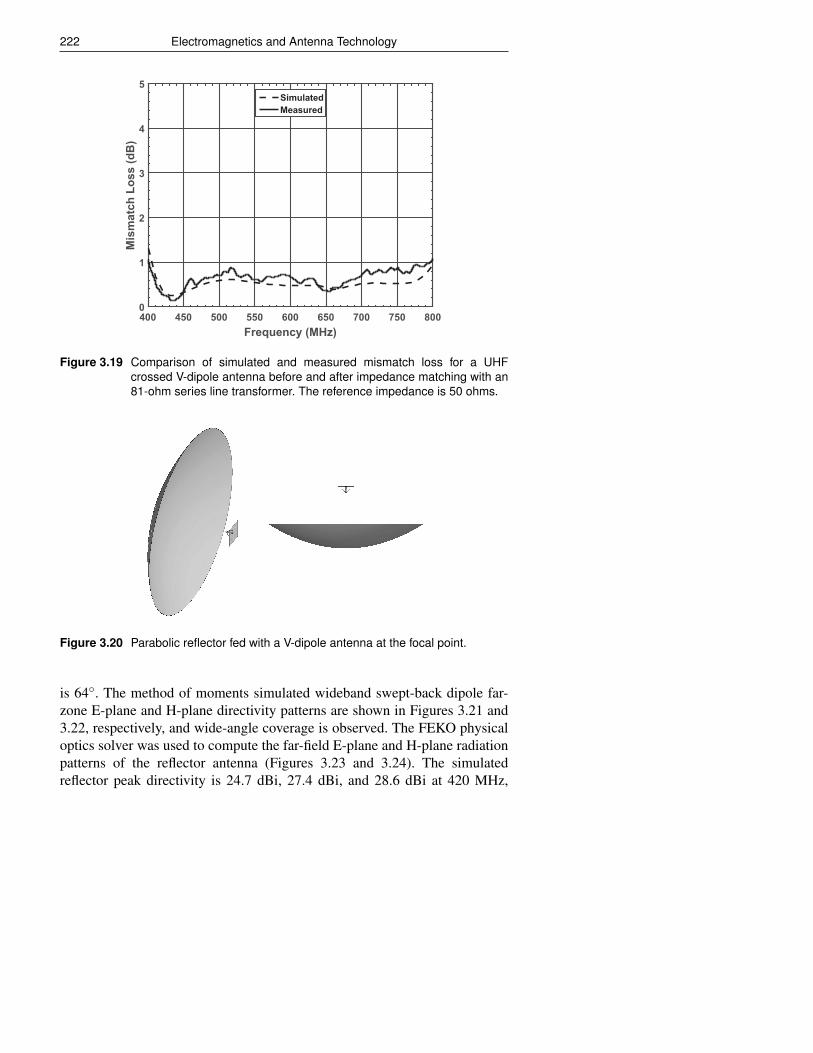
222 Electromagnetics and Antenna Technology
400 450 500 550 600 650 700 750 800Frequency (MHz)
0
1
2
3
4
5
Mis
mat
ch L
oss
(dB
)
SimulatedMeasured
Figure 3.19 Comparison of simulated and measured mismatch loss for a UHFcrossed V-dipole antenna before and after impedance matching with an81-ohm series line transformer. The reference impedance is 50 ohms.
Figure 3.20 Parabolic reflector fed with a V-dipole antenna at the focal point.
is 64. The method of moments simulated wideband swept-back dipole far-zone E-plane and H-plane directivity patterns are shown in Figures 3.21 and3.22, respectively, and wide-angle coverage is observed. The FEKO physicaloptics solver was used to compute the far-field E-plane and H-plane radiationpatterns of the reflector antenna (Figures 3.23 and 3.24). The simulatedreflector peak directivity is 24.7 dBi, 27.4 dBi, and 28.6 dBi at 420 MHz,
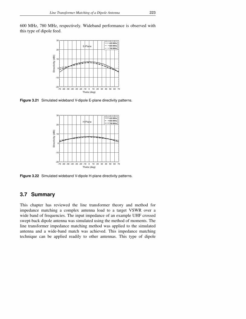
Line Transformer Matching of a Dipole Antenna 223
600 MHz, 780 MHz, respectively. Wideband performance is observed withthis type of dipole feed.
-70 -60 -50 -40 -30 -20 -10 0 10 20 30 40 50 60 70Theta (deg)
-20
-10
0
10
20
30
Dire
ctiv
ity (d
Bi)
420 MHz600 MHz780 MHz
E-Plane
Figure 3.21 Simulated wideband V-dipole E-plane directivity patterns.
-70 -60 -50 -40 -30 -20 -10 0 10 20 30 40 50 60 70Theta (deg)
-20
-10
0
10
20
30
Dire
ctiv
ity (d
Bi)
420 MHz600 MHz780 MHz
H-Plane
Figure 3.22 Simulated wideband V-dipole H-plane directivity patterns.
3.7 Summary
This chapter has reviewed the line transformer theory and method forimpedance matching a complex antenna load to a target VSWR over awide band of frequencies. The input impedance of an example UHF crossedswept-back dipole antenna was simulated using the method of moments. Theline transformer impedance matching method was applied to the simulatedantenna and a wide-band match was achieved. This impedance matchingtechnique can be applied readily to other antennas. This type of dipole
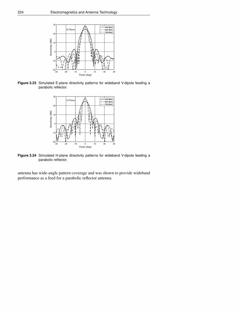
224 Electromagnetics and Antenna Technology
-45 -30 -15 0 15 30 45Theta (deg)
-20
-10
0
10
20
30
Dire
ctiv
ity (d
Bi)
420 MHz600 MHz780 MHz
E-Plane
Figure 3.23 Simulated E-plane directivity patterns for wideband V-dipole feeding aparabolic reflector.
-45 -30 -15 0 15 30 45Theta (deg)
-20
-10
0
10
20
30
Dire
ctiv
ity (d
Bi)
420 MHz600 MHz780 MHz
H-Plane
Figure 3.24 Simulated H-plane directivity patterns for wideband V-dipole feeding aparabolic reflector.
antenna has wide-angle pattern coverage and was shown to provide widebandperformance as a feed for a parabolic reflector antenna.

Line Transformer Matching of a Dipole Antenna 225
References
[1] Allen, J., “Gain and Impedance Variation in Scanned Dipole Arrays,” IEEE Trans.Antennas and Propagat., Vol. 10, No. 5, 1962, pp. 566-572.
[2] Hansen, R.C., (ed.), Microwave Scanning Antennas, Vol. 2, Los Altos, CA: PeninsulaPublishing, 1985, pp. 162-170, 301-308.
[3] Hansen, R.C., Phased Array Antennas, New York: Wiley, 1998, pp. 273-303.
[4] Kraus, J.D., Antennas, 2nd ed., New York: McGraw-Hill, 1988, pp. 435-496.
[5] Mailloux, R.J., “Phased Array Theory and Technology,” Proc. IEEE, Vol. 70, No. 3,1982, pp. 246-291.
[6] Mayer, E.D., and A. Hessel, “Feed Region Modes in Dipole Phased Arrays,” IEEETrans. Antennas Propagat., Vol. 30, No. 1, 1982, pp. 66-75.
[7] Stark, L., “Comparison of Array Element Types,” in Phased Array Antennas (Proc.1970 Phased Array Antenna Symp.), A.A. Oliner and G.H. Knittel, (eds.), Dedham,MA: Artech House, 1972, pp. 51-66.
[8] Knittel, G.H., (Brookner, E., ed.), Chapter 21 in Radar Technology, Dedham, MA:Artech House, 1977, pp. 289-301.
[9] Fenn, A.J., “Element Gain Pattern Prediction for Finite Arrays of V-Dipole Antennasover Ground Plane,” IEEE Trans. Antennas Propagat., Vol. 36, No. 11, 1988, pp. 1629-1633.
[10] Schelkunoff, S.A., and H.T. Friis, Antennas: Theory and Practice, New York: Wiley,1952, pp. 499-502.
[11] Schuman, H.K, D. R. Pflug, and L. D. Thompson, “Infinite Planar Arrays of ArbitrarilyBent Thin Wire Radiators,” IEEE Trans. Antennas Propagat., Vol. 32, No. 4, 1984,pp. 364-377.
[12] E. Brookner, B. Porter, K. Chang, Y.-C. Chang, D. Zwillinger, B. Considine, T. SikinaDemonstration of accurate prediction of PAVE PAWS embedded element gain, 2010IEEE International Symposium on Phased Array Systems and Technology, pp. 417 -422.
[13] Jasik, H., Antenna Engineering Handbook, New York: McGraw-Hill, 1961, p. 30-3.
[14] J.D. Kraus, Antennas. New York: McGraw-Hill, 1950.
[15] W.L. Stutzman and G.A. Thiele, Antenna Theory and Design, 2nd ed. New York: Wiley,1998.
[16] J. Volakis, ed., Antenna Engineering Handbook, 4th ed. New York: McGraw-Hill, 2007.
[17] C.A. Balanis, Antenna Theory and Design, 3rd ed. New York: Wiley, 2005.
[18] A.J. Fenn, Adaptive Antennas and Phased Arrays for Radar and Communications.Norwood, Mass.: Artech House, 2008.

226 Electromagnetics and Antenna Technology
[19] E. Brookner, “Phased-Array Radars,” Scientific American, vol. 252, no. 2, 1985, pp. 94–102.
[20] A.J. Fenn, D.H. Temme, W.P. Delaney, and W.E. Courtney, “The Development ofPhased Array Radar Technology,” Lincoln Laboratory Journal, vol. 12, no. 2, 2000,pp. 321–340.
[21] J.L. Allen, L. Cartledge, W.P. Delaney, and J. Dibartolo, et al., “Phased Array RadarStudies, 1 July 1959 to 1 July 1960,” Technical Report 228, MIT Lincoln Laboratory,12 Aug. 1960, DTIC no. AD-0249470.
[22] J.L. Allen, L. Cartledge, W.P. Delaney, and J. Dibartolo, “Phased Array Radar Studies,1 July 1960 to 1 July 1961,” Technical Report 236, MIT Lincoln Laboratory, 13 Nov.1961, DTIC no. AD-271724.
[23] J.L. Allen, D.M. Bernella, W.W. Carpenter, and W.P. Delaney, “Phased Array RadarStudies, 1 July 1961 to 1 July 1963,” Technical Report 299, MIT Lincoln Laboratory,20 Feb. 1963, DTIC no. AD-417572.
[24] J.L. Allen, D.M. Bernella, F. Betts, and L. Cartledge, “Phased Array Radar Studies, 1July 1963 to 1 July 1964,’ Technical Report 381, MIT Lincoln Laboratory, 31 March1965, DTIC no. AD-629363.
[25] R.J. Mailloux, “Phased Array Theory and Technology,” Proc. IEEE, vol. 70, no. 3, 1982,pp. 246–291.
[26] J.L. Allen, “Gain and Impedance Variation in Scanned Dipole Arrays,” IRE Trans.Antennas and Propagation, vol. 10, no. 5, 1962, pp. 566–572.
[27] J.L. Allen and W.P. Delaney, “On the Effect of Mutual Coupling on Unequally SpacedDipole Arrays,” IRE Trans. Antennas and Propagation, vol. 10, no. 6, 1962, pp. 784–785.
[28] J.L. Allen, “On Array Element Impedance Variation with Spacing,” IRE Trans.Antennas and Propagation, vol. 12, no. 3, 1964, pp. 371–372.
[29] J.L. Allen, “On Surface-Wave Coupling Between Elements of Large Arrays,” IEEETrans. Antennas and Propagation, vol. 13, no. 4, 1965, pp. 638–639.
[30] H.K. Schuman, D.R. Pflug, and L.D. Thompson, “Infinite Planar Arrays of ArbitrarilyBent Thin Wire Radiators,” IEEE Trans. Antennas Propagation, vol. 32, no. 3, 1984,pp. 364–377.
[31] A.J. Fenn, P.T. Hurst, J.D. Krieger, J.S. Sandora, and L.I. Parad, “UltrawidebandVHF/UHF Dipole Array Antenna," 2010 IEEE International Symposium on PhasedArray Systems and Technology, Waltham-Boston, Mass., 2010, pp. 79–82.
[32] K.E. Schmidt, “Mutual Impedance of Nonplanar Skew Dipoles," IEEE Trans. Antennasand Propagation, vol. 44, no. 9, 1996, pp. 1298–1299.
[33] H.J. Reich, ed., Harvard Radio Research Laboratories, Very High Frequency Techniques,New York: Mc-Graw Hill, Vol. 1, Chapter 3, 1947.
[34] R.L. Thomas, A Practical Introduction to Impedance Matching, Dedham, MA: ArtechHouse, 1976.
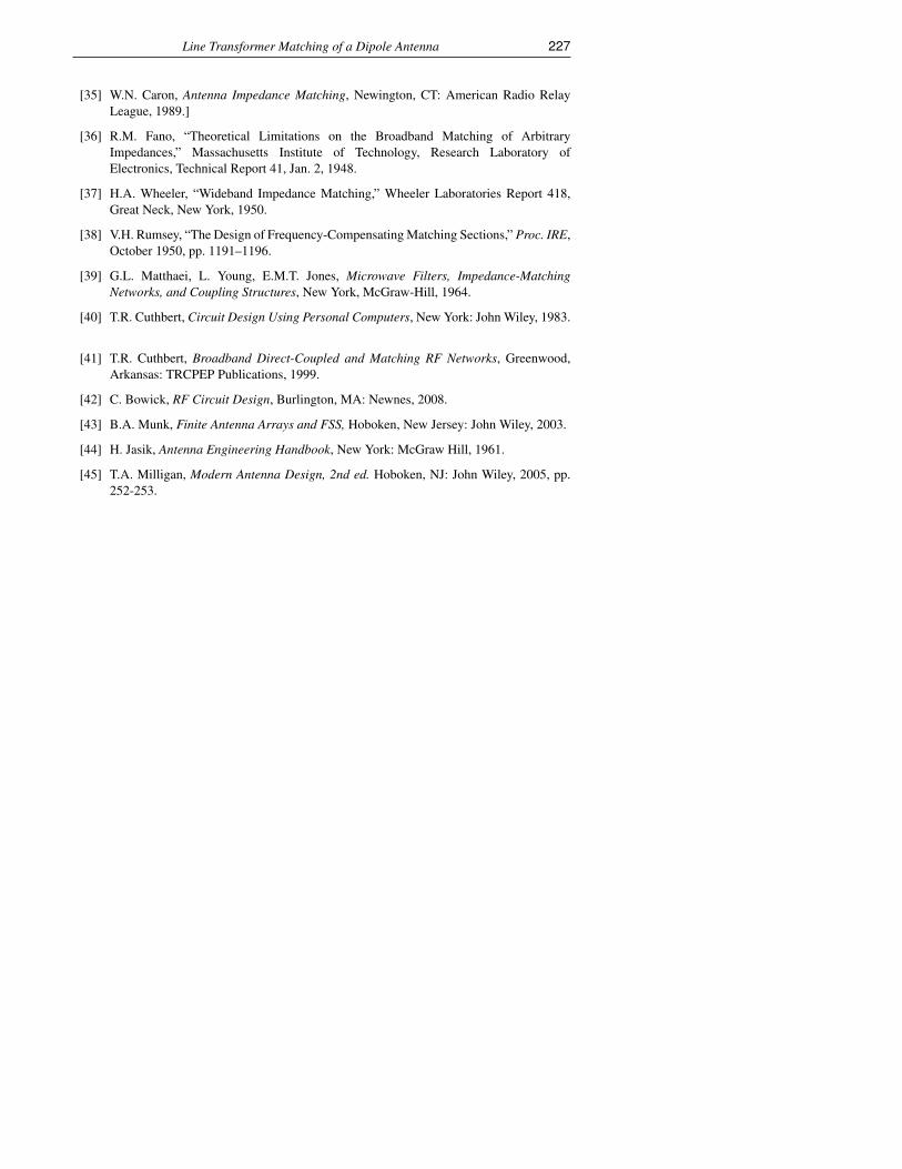
Line Transformer Matching of a Dipole Antenna 227
[35] W.N. Caron, Antenna Impedance Matching, Newington, CT: American Radio RelayLeague, 1989.]
[36] R.M. Fano, “Theoretical Limitations on the Broadband Matching of ArbitraryImpedances,” Massachusetts Institute of Technology, Research Laboratory ofElectronics, Technical Report 41, Jan. 2, 1948.
[37] H.A. Wheeler, “Wideband Impedance Matching,” Wheeler Laboratories Report 418,Great Neck, New York, 1950.
[38] V.H. Rumsey, “The Design of Frequency-Compensating Matching Sections,” Proc. IRE,October 1950, pp. 1191–1196.
[39] G.L. Matthaei, L. Young, E.M.T. Jones, Microwave Filters, Impedance-MatchingNetworks, and Coupling Structures, New York, McGraw-Hill, 1964.
[40] T.R. Cuthbert, Circuit Design Using Personal Computers, New York: John Wiley, 1983.
[41] T.R. Cuthbert, Broadband Direct-Coupled and Matching RF Networks, Greenwood,Arkansas: TRCPEP Publications, 1999.
[42] C. Bowick, RF Circuit Design, Burlington, MA: Newnes, 2008.
[43] B.A. Munk, Finite Antenna Arrays and FSS, Hoboken, New Jersey: John Wiley, 2003.
[44] H. Jasik, Antenna Engineering Handbook, New York: McGraw Hill, 1961.
[45] T.A. Milligan, Modern Antenna Design, 2nd ed. Hoboken, NJ: John Wiley, 2005, pp.252-253.


