Embed Size (px)
Citation preview

BestAvailable.
Copy

0i OFFICE OF NAVAL RESEARCH
in GRANT or CONTRACT: N00014-91-J-1919
iN iR&T Code 4133036Robert Nowak
0 Technical Report No. 13
Electrochemical Atomic Layer Processing
Choong K. Rhee, Baoming M. Huang, Elvin M. Wilmer,Sajan Thomas and John L Stickney .... DTIC
In Pr'ess ELECTE
for JUL 2 1994
Materials and Manufacturing Processes GDepartment of Chemistry
University of GeorgiaAthens, GA 30602-2556
6/24/94 94-22623
Reproduction in whole, or in part, is permitted for any purpose of the United StatesGovernment.
This document has been approved for public release and sale;its distribution is unlimited.
047 9 108

-I Form -p rove
REPORT DOCUMENTATION PAGE o1. No o0o7.o019"* ~ - ;:. 30co t. -11- 4 % OCh .. 4IE ' **q 41 iOtto
1 t-M W tofe le o4 -stru. "SIl . *&F(AF00 08.11Slq4414 ~(4"
~ .~1 we~' ,' U 9' tod i ovowpqton -4seeunenW' iwvtMEL owenorew F& w'JPU44( oopgotmw s" gee,. 14 IS ,.01e,4W
b .a. .t '2.4 .1 M . 30 V4JJO telo 1". 00W 11 %.0"WAeqw.tVSadtaeet 0.4 040.'Wt d96 P OdW O 44 16). *aah..0a. CC Ale
I. AGENCY USE ONLY (Leave blank) I . REPORT DATE 3. REPORT TYPE AND DATES COVERED6/25/94 Technical - 1. June
4. TITLE AND SUBTITLE S. FUNDING NUMBERS
Electrochemical Atomic Layer Processing G-NO0014-19-J-1919
6. AUTHOR(S)
Choong K. Rhee, Baoming H. Huang, Elvin H. Wilmer,Sajan Thomas and John L. Stickney
7. PERFORMING ORGANIZATION NAME(S) AND ADORESS([S) IL PERFORMING ORGANIZATION
John L. Stickney REPORT NUMIIERDepartment of ChemistryUniversity of Georgia Technical Report #13Athens, GA 30602-2556
I. SPONSORING. MONITORING AGENCY NAME(S) AND ADDRESS(ES) 10. SPONSORING /MONITORINGAGENCY REPORT NUMBER
Office of Naval ResearchChemistry DivisionArlington, VA 22217-5000
11. SUPPLEMENTARY NOTES
t2a. DISTRIBUTION AVAILABILITY STATEMENT 12b. DISTRIBUTION CODK
Approved for public release and sale;
its distribution is unlimited
13. ABSTRACT (Maximum 200 words)
Atomic layer processing with electrochemical control is discussed. A method for the electro-deposition of compound semiconductors based on the principles of atomic layer epitaxy (ALE) is reported,with specific reference to the formation of ZnTe. This method is referred to as electrochemical atomiclayer epitaxy (ECALE). A number of II-VI compounds have been formed using this method, including:CdTe, CdSe, CdS, ZnTe, ZnSe, ZnS and HgSe. Initial studies of GaAs and PbSe have also been pursued.A computer-controlled electrochemical flow deposition system is described. The system has beenconstructed to form thin-films of the compounds listed above using the ECALE methodology. In addition,an analogous digital electrochemical etching procedure has been developed, and used to etch CdTesubstrates. The etching cycle consists of oxidizing off the top atomic layer of Cd atoms at a relativelypositive potential, followed by Microscopy (AFM) has been used to image the resulting features. ECALEand the digital electrochemical etching process are both based on selecting potentials where an atomic layerof an element is deposited, or removed, in a surface limited reaction. The potentials used are referred toas underpotentials in the electrochemical literature. The atomic layer deposition process is referred to asunderpotential deposition (UPD).
14. SUBJECT TERMS 15, NUMBER OF PAGESECALE, CdTe, Digital etching, surfaces analysis, flow cell, 28
electrochemistry 16. "At CODE
17. SECURITY CLASSIFICATION 11. SECURITY CLASSIFICATION It. SECURITY CLASSIFICATION 20. LIMITATION OF ABSTRACTO@ REPORT OF THIS PAGE OF ABSTRACTUnclassified Unclassified Unclassified UL
NSN 7S40-01-29-00 ,t Standard Form 298 (Rev 2-89)few aob A14U MA 1".16

Electrochemical Atomic Layer Process'ng
Choong K. Rhee, Baoming M. Huang, Elvin M. Wilmer, Sajan Thomas and John L. Stickney*.
Department of Chemistry, University of Georgia, Athens, Georgia 30602-2556.
*To whom correspondence should be addressed.

Key words
ZnTeCdTe
UnderpotentiaiElectrochemical atomic layer epitaxyECALEElectrochemical etchingDigital etchingAtomic force microscopyAFMScanning tunneling microscopySUMThick layer cellThin layer cellFlow cell

ABSTRACT
Atomic layer processing with electrochemical control is discussed. A method for theelectrodeposition of compound semiconductors based on the principles of atomic layer epitaxy(ALE)D is repered. with specific reference to the formation of ZnTe. This method is -eiferred to aselectrochemical atomic layer epitaxy (ECALE). A number of II-VI compounds have been formedusing this method, including: CdTe, CdSe, CdS, ZnTe, ZnSe, ZnS and HgSe. Initial studies ofGaAs and PbSe have also been pursued. A computer-controlled electrochemical flow depositionsystem is described. The system has been constructed to form thin-films of the compounds listedabove using the ECALE methodology. In addition, an analogous digital electrochemical etchingprocedure has been developed, and used to etch CdTe substrates. The etching cycle consists ofoxidizing off the top atomic layer of Cd atoms at a relatively positive potential, followed byreducing off the top layer of Te atoms at a relatively negative potential. Atomic ForceMicroscopy (AFM) has been used to image the resulting features. ECALE and the digitalelectrochemical etching process are both based on selecting potentials where an atomic layer of anelement is deposited, or removed, in a surface limited reaction. The potentials used are referredto as underpotentials in the electrochemical literature. The atomic layer deposition process isreferred to as underpotential deposition (UPD).

77¸
Introduction
Atomic Layer Epitaxy (ALE) is a deposition methodology in which a cycle is used todeposit compounds "digitally", one monolayer at a time (1-4). Although ALE has beendeveloped primarily as an application of Chemical Vapor Deposition (CVD) or Molecular BeamEpitaxy (MBE), the principles have recently been applied in the electrochemical deposition ofcompound semiconductors (5-9). As in ALE, Electrochemical Atomic Layer Epitaxy involves adeposition cycle, at separate potentials, in the ECALE cycle. Atomic layers of each element aredeposited from separate solutions. Deposition is limited to an atomic layer by usingunderpotentials to deposit each element. Underpotential deposition refers to a phenomenonwhere, due to the heat of compound formation, one element deposits on a second element at apotential prior to (under) that necessary to deposit the element on itself(10). Classically, UPDhas been associated with the deposition of one metal on a second, which is referred to here asreductive LPD (10) In addition, there are a number of systems where oxidative LPD isobserved. This involves the deposition of an atomic layer of an element by oxidation of a reducedform of the element. Again, an atomic layer of the element deposits at a potential prior to thatneeded to deposit the element on itself Examples of oxidative UPD include: I onto Am (11),oxygen onto Cu (12), As onto Au (8), and Te onto Au (13).
The ECALE methodology requires an exchange of solution after the deposition of eachcomponent element. Each element is deposited from a solution designed specifically for thedeposition of that element. The solution pH is a major variable. Blank solutions, correspondingto the deposition solutions, are used between the deposition solutions. In this way, the precursorto one element can be flushed out of the cell with its corresponding blank solution prior tointroduction of solutions containing precursors to the subsequently depositing elements.
Presently, deposits are formed in a thin-layer electrochemical celi (14). Thin-layer cellsare used for a number of reasons: they keep the quantity of solution (1-10 gL cm -) needed for agiven deposition step to a minimum; the lower volumes of solutions result in lower amounts ofany solution-born contaminants; and thin-layer cells can be designed to facilitate exchange of thesolution in contact with the electrode.
Manual thin-layer cells have been used extensively in ECALE studies. Due to the largenumber of steps making up each ECALE cycle, however, use of a manual thin-layer cell becomestedious and reproducibility drops, especially for deposits formed with more than 10 cycles. Acomputer-controlled electrochemical thin-layer flow-cell is presently being used to form depositswith more than 10 cycles.
In addition to compound formation using the ECALE methodology, an electrochemicalform of "Digital Etching" (15) has been developed in this group (16). The process is essentiallythe inmerse of ECALE, in that UPD potentials are used as stripping potentials for the individualelements in a compound. That is, a low potential is first used to reduce off the top layer of oneelement, by forming a soluble anionic species. A mc re positive potential is then use. z1- oxidizeoff the top layer of the other element, by forming a soluble cationic species. Pure electrolyte iscontinuously flushed over the substrate to rinse away the product ions. Only the top layer of an
2

element is removed in this procedure, since the potential is kept below that needed to strip theelement from the bulk of the compound, where the element is fully coordinated.
Table 1. Status of compound formation by ECALE.
11-VI 0 S Se Te
Zn YES? YES YESCd YES YES YES
Hg YES U
IV-VI 0 S Se Te
Sn P P PPb P YES U
lll-V N P As Sb Bi
AlGa YES? PIn P PTI P P
P-Probably, but has not yet been investigated
U=Under investigation; ?=Not yet clear, but has been studied
Initial ECALE studies have centered on investigations of CdTe deposition (5-7).Subsequent work has taken a number of directions, including findamental atomic level =tdies ofthe growth of the first two monolayers of CdTe on Au single crystals (13, 17, 18). ECALEcycles are being developed for the deposition of other compounds as well. Cycles have beendeveloped for CdTe (5-7), GaAs (7, 8), CdS (19), CdSe, ZnSe, and PbSe (Table 1). Recentstudies of ZnTe deposition are presented in this article.
Experimental
A diagram of the electrochemical flow-cell system used for ECALE deposition is shown inFIG. 1. A simplified version of the same instrument may be used for digital electrochemicaletching. It consists of a thin-layer electrochemical flow-cell, interfaced to a distribution valve.PEEK tubing is used to plumb :t-e system, due to its low oxygen permeabi!ity. Distribut:on valveswith four or six inlets and a single outlet were used, as two solutions are needed for each elementdeposited. The solutions used to deposit a given element have their pH and supporting electrolyte
3

optimized for the deposition of that element. A corresponding blank solution was also used inorder to rinse away excess reactant prior to introduction of the next reactant solution. Thefour-way valve was used for the formation of binary compounds, while a new system uses asix-way valve in order for three elements to be deposited. This system will be used for theformation of ternary compounds, superlattices, and for doping studies.
Because the cell volumes were on the order of 10 mL or less, accurate pumping wasrequired. Microliter pipeting pumps designed to deliver aliquots of 2 to 25 mL in a single shot, orsmall parastaltic pumps were used. The solution reservoirs were made with Pyrex glass bottlesand Teflon valves.
The design of the flow-cell (FIG. 1) is similar to those available commercially. The faceplate of the cell was made of Plexiglass, since it allowed visual inspection of the depositing films.A Teflon gasket, 0.005" thick, with an oblong hole sufficient to encompassing the inlet and
outlet, was placed on the inside of the Plexglass face plate. The inlets and outlets were tapped1/4-28 for attachment of the plumbing.
The substrates were 0.010" Au foil and were supported by a Plexiglass or stainless steelblock which swiveled on the end of a bolt with a hemispherical head. A torque wrench was usedto reproducibly tighten the bolt and compress the cell. The bolt was set in a stainless steelU-block (FIG. 1). A separate compartment, attached to the cells' exit stream, was used for thereference and auxiliary electrodes. The compartment was separated from the flow stream by aporous Vicor plug.
Manual thin-layer electrochemical cells were used, as well (6). These electrodes consist ofan Au rod set in a fitted glass cavity. The glass walls were designed to be on the order of 0.001"from the Au rod. Two pin holes were ground into the bottom of the glass in order for thesolution to be flushed in and out of the thin-layer cavity. In addition, the holes provide a path forionic conductivity. Cell volumes were on the order of 3-4 mL, for an electrode area of 1-1.4 cm".Application of a slight excess of N2 pressure inside the cell, flushes solution from the cell. If thecell is then placed in contact with a new solution, and the N2 pressure is released, an aliquot ofthe new solution will wick into the cell by capillary action. The result is a complete exchange ofsolution, a rinse.
Solutions were prepared with water from a Nanopure water filtration system, fed from thehouse deionized water supply, and analytical grade reagents. The potentiostats were builtin-house using a conventional op-amp based design. All potentials are reported versus theAgIAgCI (IM NaCI) reference electrode.
Results and Discussions
4

ZnTe Formation
The formation of ZnTe serves an example of electrochemical ALE. FIG. 2 is a series ofcyclic voltammograms depicting the deposition of Zn and Te on polycrystalline Au in a manual:i-"-a',e electroch me•:al cell. FIG. 2a is a scan of the clean Au electrode in I M HKSO. Thebasic features of the v oitammogram are the oxidation of the Au surface at high potentials and thesubsequent reduction of the Au oxide on the negative ping scan. Hydrogen evolution is visibleas the negative limit of the voltammogram. A negative scan from the rest potential with analiquot of a 0.25 mM TeO2 solution, pH 3, is shown in FIG. 2b. A UPD peak at 0.25 V and abulk deposition peak at -0.05 V are evident in the voltammetry. The negative limit in thevoltammetry corresponds to hydrogen formation. FIG. 2c is voltammetry for the Au electrodecovered with two monolayers of Te in a borate solution buffered at pH 8.6. A distinct feature isvisible at -1.0 V, corresponding to the reduction bulk Te to telluride ion, Te•. Reversal ofthescan direction results in the reoxidation of the Te' to Te. Studies have shown (5) that rinsingwith a blank solution at potentials below -1.1 V removes the Tea, leaving only an atomic layer ofTe (dashed curve in FIG. 2c). This process is referred to as oxidative Te UPD. Oxidative TeUPD involves the reaction:
{I} Te2 = Te (ad) + 2e-
as opposed to reductive Te UPD which involves the reaction:
(2} HTeO,2 + 4e = Te (ad) + H'.
Ideally, a species such as Te: would be used for the formation of atomic layers of Te by oxidativeLPD in the ECALE f.-mation of Te containing compounds. The instability of Te2- containingsolutions, however, m -_kes this impracticable. This procedure does work in the ECALE formationof sulfur containing compounds (19). Solutions of S' are stable and can be oxidized to formsulfur atomic layers. Oxidative UPD of both Se and Te are, however, performed inversely.Instead of oxidizing an atomic layer of Te onto the surface from a Te" solution, bulk Te is firstdeposited by reductiorn from a HTeO2 solution. Excess (bulk) Te is then reductively strippedaway in a blank solution, leaving an atomic layer of Te.
After the formation of a Te atomic layer, Zn was deposited by exchanging the solution for10 mM ZnSO, and reducing at -1.0 V. FIG. 2d displays the voltammetry associated with thedeposition of Zn on a- atomic layer of Te. At -0.7 V a shoulder appears, which corresponds toreductive Zn UPD or'. :,.e Te. At more negative potentials a steeply increasing reduction currentis observed, which corresponds to the deposition of bulk Zn and the evolution of H-2.
Voltamrnmetrv z'.:ch as that in FIG. 2, was used to develop an ECALE cycle for the:crma;b:n ofZn e. ..• cyc.e started with Te deposition at -1.0 V from a 0.4 nI TeOO solution.borate buffered at pH 3.6 with I M NaCIO, as a supporting electrolyte. The solution was then
5

exchanged for an equivalent blank solution, containing no TeO2, and rinsed three times at -1.30 V,completing oxidative Te UPD.
Zn was then deposited from a 10 mM ZnSO4 solution, buffered with phthalate at pH 5.2and containing 0.5 M Na,:SO4 as a supporting electrolyte with the potential poised at -I 0 V. Thecvc!e was completed by rinsing with the corresponding Zn blank solution three times
Studies of the coverages of Zn and Te resulting from diffiag numbers of cycles up to16, were performed using a manual thin-layer cell Coverages were determined in-situ byelectrochemically stripping the resulting deposits. FIG. 3 displays the stripping voltammetry, fordeposits formed from 2, 8 and 16 ECALE cycles, in 0.5 M N&;SO4 + 0.5 M phthalate. There arefour oxidation features visible in the stripping scan. The first two, at -0.6 and -0.2 V, correspondto the stripping of Zn from the deposit in a two electron process forming Zn÷. The second two,at 0.1 and 0.4 V, correspond to the oxidation of the Te to HTeOC' in a four electron process (eq(2)). Zn and Te coverages were obtained by integration of the peak areas, and the data areshown in FIG. 4. The lattice constant for ZnTe is 0.61 nm, whereas twice the Au-Au distance inthe Au(100) plane is 0.584 nm, resulting in a 4% lattice mismatch. If we assume epitaxialdeposition on the Au surface with a 4% contraction in the ZnTe lattice, one cycle should result inthe deposition of a 1/2 monolayer of Zn and a 1/2 monolayer of Te, where a monolayer refers tothe number of surface Au atoms. The solid line shown in FIG. 4 corresponds to the deposition of1/2 monolayer per ECALE cycle. The surface area of the electrode was taken to be the geometricsurface area multiplied by a roughness factor of 1.2. The average Au surface atomic density forthe polycrystalline Au electrode was taken to be that of a Au(100) surface, 1.2 x 10"' atom&'cmra:Experience has shown these assumptions to hold for similar electrodes within about 10%.
For deposits made with less than about 10 cycles, the Zn coverage is a little high relativeto the 1/2 monolayer per cycle line, while the Te coverage is a little low (FIG. 4). At 16 cycles,both Te and Zn coverages are low by about 15% relative to the 1/2 monolayer/ cycle line. Thereasons for the initially high Zn coverage appear to be related to the first Zn oxidation peak. I: iswell formed, after only 2 cycles (FIG. 3a), and it remains nearly constant in size as the number ofcycles increases. After the second cycle, it is only the second Zn stripping peak at -0.2 V whichcontinues to grow.
The nature of the first Zn stripping peak is not clear. It is expected that the top layer ofZn will oxidize off at a less positive potential than Zn completely coordinated to Te in the deposit.The first Zn stripping peak, however, corresponds to more than the 1/2 monolayer of Zn expectedfor stripping the top Zn atomic layer.
After 10 cycles, the curves for Zn and Te both drop down, relative to the 1/2 monolayerper cycle line. The reasons for this are also not clear. The potentia!s needed for optimal 1/2monolayer deposition may vary as the deposit grows. It may simply be increased operator error.Depositing 16 cycles with a manual thin-layer cell is very tedious. The trend in coverage per cyclewill be the subject of future studies using the computer-controlled flow-cell described in the nextsection. Besides operator error or a change in the optimal depositicn potentials, exar2natic, :.FIG. 3c shows that the base line resolution between Zn stripping and Te stripping, is disappearing
6

at the 16 cycle level. In addition, it is probably difficult to completely strip the Zn from a depositmade from 16 cycles. It however, not all the Zn was stripped by the completion of the secondZn stripping peak. it would be expected to oxidize during the Te stripping features, increasing theobserved Te stripping charge. The Te charge, however, decreased as well.
Flow-cell
As mentioned, the use of a manual thin-layer cell for more than about 10 cycles, provestedious. The computer-controlled flow-cell deposition system, described in the experimentalsection (FIG. 1), is presently being used to form thicker deposits without the operator errorinherent in manual thin-layer studies. FIG 5 describes the program used to deposit CdTe in theflow-cell deposition system. Prior to application of the ECALE cycle, the 0.01" Au foil substrateswere cleaned by etching in nitric acid and then annealed in a gas oxygen flame. The cell was thenassembled and torqued together. Voltammetric cycles were run in I M -ISO.. in order to assuresubstrate cleanliness, prior to initiation of the deposition program.
The program in FIG. 5 was the first used to make CdTe deposits with the flow cell. TheECALE cycle (FIG 5) began with the introduction of the HTeO,. solution at open circuit. Opencircuit was used in order to avoid depositing most of the Te at the entrance of the cell. Five 15IL aliquots of the HTeO,÷ solution were used to exchange the system volume, where the systemvolume includes the solution in the outlet of the distribution valve, in the cell, and in the tubingleading up to the cell. After the HTeO2* solution was introduced to the cell, it was held quiescentwhile deposition was carried out at -0.8 V, a potential where all HTeO.$ present in the cell wasdeposited. The cell volume was sufficiently small that only a few monolayers of Te weredeposited. The electrode potential was then allowed open circuit, while the system volume wasflushed with the Te blank solution, removing any remaining HTeO,*. If the potential had beenheld at -0.8 V while the remaining HTeO2÷ was flushed through the celi, the HTeO2* presentwould have deposited at the entrance to the cell, and would have proven difficult to remove. Thepotential was nex: s.n:,ied to -1.25 V and held, filled with the blank solution. Bulk Te is unstableat -1.25 V, forming Te' which is soluble. The cell was then flushed out multiple aliquots of theTe blank solution. The Cd blank solution was then introduced and the potential shifted to -0.6 V,the Cd UPD potential. The To and Cd deposition solutions differed by several pH units, and useof the Cd blank solution served to condition the tubing and cell, prior to introduction of the Cdsolution itself This prevented Cd(OH-I formation. The CdSO4 solution was then introduced andCd was deposited at -0.6 V, with the solution quiescent. Finally, excess CdSO4 was swept fromthe cell using aliquots of the Cd blank solution followed by the Te blank solution, and the cyclewas begun again.
FIG. 6 depicts Cd and Te coverages, and the Te/Cd ratio, for deposits made with 50ECALE cycles, as a %jnction of the Cd UPD potential. The coverages are relative, determinedusing Electron Probe .Micro Analysis (EPMA). Some ICP-AES experiments were performed toobtain absolute Cd coverages, however. Selected deposits were dissolved in nitric acid andanal•zed f"r total Cd contents. These results were then used to calibrate the EPMA data. At Cdpoteni:;ais abo% e -0., V, a sharp drop-off in Cd coverage is observed. The Te coverage drops aswell, pointing out the dependence of the Te coverage on the presence of Cd at the surface. The
7

Te/Cd ratio was a little high at -0.4 V, as well, but the stoichiometry is still 1:1. A plateau isevident between -0. 6 V and -0.7 V, at a coverage very close to the predicted 1/2 monolayer of Cdand 1/2 monolayer of Te per cycle. At the most negative potential, -0.8 V, the coverages of boththe Cd and Te increased significantly. This increase was anticipated, as bulk Cd begins to depositin this potential range. It is interesting to note, however, that the stoichiometry remains 1:1 overthe entire range of Cd deposition potentials studied.
Deposits of CdTe have been formed using the program in FIG. 5 with from 10 to 100cycles. FIG. 7a is a diagram of the surface coverages of Cd and Te in CdTe deposits made withincreasing numbers of cycles, determined in arbitrary units with EPMA. FIG. 7b shows that thestoichiometry of the deposits, again, remains close to 1:1, as the number of cycles is increased.The relative Te coverage, however, drops a little after 100 cycles. A dramatic increase in theslope of the graph above 50 cycles indicates that the coverage per cycle is increasing for thesethicker deposits. The cause of this increase is clearly seen in the electron micrographs shown inFIG. S. At 50 cycles, a series of 100-200 nm particles appear. As the number of cycles is firtherincreased, clumps of particles are observed. Evidently, the increased coverages at high cyclenumbers is the result of an exponential increase in surface area due to increased surfaceroughness. Again, it is interesting to note that the stoichiometry of the deposits itmains nearly1:1, even while the surface is roughening.
Presently, the causes of the fbrmation of these particles are under investigation. One lineof investigation underway in our group involves STM studies of islands on the Au substrates.These islands appear to be formed during the electrochemical cleaning cycles, prior to deposition.FIG. 9 is a STM micrograph of some of these islands. Their heights correspond to atomicallyhigh Au islands. The increased number of surface defects associated with the presence of theseislands may contribute to the nonideal deposit morphology. The islands appear to be the resultof the formation and removal of surface reconstructions on the Au (20, 21). The reconstructedsurfaces are formed upon annealing and involve a higher surface density of atoms. Positivepotentials used during the cleaning cycles, serve to lift the reconstructions, freeing up the excesssurface atoms. The result is that the excess Au atoms coalesce into islands. Another likely sourceof the observed particles involves unflushed solution volumes in the cell, tubing, or valves. If Te'formed during the cycle comes in contact with solution containing Cde, they can homogeneouslyprecipitate and adsorb on the deposit surface. These adsorbed particles could then act asnucleation centers. Work with the cell design and rinsing procedures are under way to try andeliminate this possibility.
Digital Electrochemical Etching
Besides studies of ECALE deposition, digital electrochemical etching of compoundsemicOnductors is being pursued (16). The electrochemical program used is essentially theinverse of the ECALE deposition program. The principle, for a compound semiconductor, is thatthe top layer of atoms is less strongly bound to the substrate than are atoms of the same elementburied deeper in the compound, that are more coordinatively saturated. It should be possible toremove this top layer of atoms at a lower potential than that required to strip atoms of the sameelement in the bulk of the compound. To digitally etch CdTe, a relatively positive potential is
8

used to oxidize the top layer of Cd atoms, but not positive enough to strip Cd from the bulk of theCdTe lattice. The Cd:" ions formed are then flushed away, leaving a layer of Te atoms as the topatomic layer. Next, a relatively negative potential is used to reduce the top layer of Te atoms toTe: ions, which are flushed away. Studies in aqueous solutions have shown that it is very difficultto reduce Te from the bulk of CdTe, regardless of how negative a potential is used. The netresult if the reduction is to remove the top atomic layer of Te, leaving a Cd terminated surface.
The potential used to oxidize the top atomic layer of Cd atoms is one of the moreimportant variables in the etching cycle. The dependence of etched depth on the Cd strippingpotential is discussed below.
A thin-layer flow-cell system, similar to that shown in FIG. 1, has been used in most of thedigital electrochemical etching studies performed thus far. It is important to completely flushproduct ions from the surface prior to changing the stripping potential. If the ions produced arenot completely flushed away, they can redeposit during the subsequent half cycle, probablycontributing to surface roughening. A CdTe (100) crystal (I-VI Inc.) was used as the substratein the present studies. An ohmic contact was made on the ' ck using high purity In and a Al foil.The etching solution used contained 0.1 MNa7SO 4 , pH 5.7. The pH 5.7 was high enough toallow Te" based species to form at -1.3 V without excessive hydrogen evolution, yet it was lowenough to avoid Cd(OH)2 formation.
Separate stripping solutions could have been used for the two cycle halves, if it weredeemed advantageous. The potentiostat was computer interfaced, although a simple functiongenerator would have been sufficient. The flow rate of the solution was a constant 1.1 mlimin.
The voltammetry in FIG. 10 is for the CdTe crystal in a thick layer cell. Both theoxidation of Cd at 0.3 V and the reduction of Te at -1.0 V are visible in the voltammetry. Use ofa potential less than -1.0 V for stripping the Te atomic layers appears reasonable fromexamination of FIG. 10. The potential needed to strip the top layer of Cd was not as clear cut.
A separate set of experiments was performed, as a flmction of the Cd stripping potential,using a thick-layer cell. The charge for the subsequent reduction of the top layer of Te atomswas used to determine the extent of Cd removal. The idea was that if the Cd stripping potentialwere too low, insufficient Cd would be removed and the subsequent reduction charge for Tewould be low. If the Cd stripping potential were too high, the Te reduction charge would be toohigh. FIG. 11 is a graph of the resulting charges for Te stripping. Those experiments wereproblematic, as the background corrections were very difficult to make. The substrate used was apiece of p-CdTe(100) with a band gap of 1.5 eV, thus the background at potentials where Te'was formed shifted significantly from run to run due to minor changes in room light. Thesedi:culties are reflected in the scattering of the data (FIG. 11). However, a distinct S curve, witha plateau between 0.05 V and 0.35 V is evident.
In order to obtain a more accurate measure of the amounts of material removed perh-inz :.cle. a second set of data on digital etching was obtained using AFIM. The depth
sensitivity of AFM is optimal for surface profiling substrates with features on the order of 50 nm
9
to 200 nm deep. To use the AFM effectively, however, the surface had to be patterned. With thesurface patterned, etching produced an ordered series of micron sized features. Profiles vwere thenused to determine etched amounts. A positive photo-resist system, AZ-1350, from HoechstCelanese was used to form the patterns.
FIG. 12 is an AFM micrograph of the surface of a digitally etched CdTe(100) surface.The crystal was initially etched in a Br2-methanol solution prior to application of the photo-resist.It was exposed using a test mask and developed leaving the photo-resist pattern on the sufce.The crystal was then incorporated into a thin-layer electrochemical flow-cell, as described above,and 300 etching cycles were performed. A surface profile drawn across an etched features isshown in FIG. 13. The etched depth appears to be 137 nm, or 0.46 nm/cycle. Based upon thelattice constant of zinc blende CdTe, which is 0.648 tin, one monolayer should be 0.324 nm thick.The ideal one cycle etch depth should thus be 0.324 nmn/cycle. These are the first AFM images ofdigitally electrochemically etched substrates. Presently, studies are underway to examine thedependence of the amount etched per cycle versus the following cycle variables: Cd etchingpotential, Te etching potential, flow rate, and solution composition. Besides optimizing theamount etched per cycle, the morphology of the resulting etched surfaces will be examined, aswell as any anisotropy in the etch walls or surfaces.
Acknowledgements
Acknowledgment is made to the Department of the Navy, Office of the Chief of NavalResearch, under Grant No. N00014-91-J-1919. Acknowledgment is also made to the NationalScience Foundation for partial support of this work under Grant No. D'MR-901743 L.
10

References(1) Suntola, T. and Antson, J., Finnish Patent No. 52359 (1974); U.S. Patent No. 4058430.
t2) Nishizawva-.-1, Abe, H., and Kurabayashi, T., J. Electrochem. Soc., lVol. 132.p. 1197(198 "); Goodman, C.H.L. and Pesssa, M.N., J. Appi. Phys.,Vol. 60, R65 (1986);DenBaars, SiP and Dapkus, P.D., J. Ciyst. Grow.,Vol. 98, p. 195(1989).
(3) Kuech, T.F., Dapkus, P.D., and Aoyagi Y., "Atomic Layer Growth and Processing", Mks,Pittsburgh, Vol. 222, 1991; Bedair, S., *Atomic Layer Epitaxy," Elsevier Sci., Amsterdam, 1992.
(4) Niuuisto, L. and Leskela, M., Thin Solid FilmsVol. 225, p. 130(1993).
(5) Gregory. B.W. and Stickney, J.L., J. Electroanal. Chem.,Vol. 300, p.543(1991).
(6) Gregory, BXW, Suggs, D.W., and Stickney, J.L., J. Electrochem. Soc.,Vol. 138,
(7) Suggs, D.W., Villegas, I., Gregory, B.W., and Stickneqy, J.L., in "Atomic Layer Growth andProcessing", Eds. Aoyagi Y., Dapkus, P.D. and Kuech, T.F., MRS, Pittsburgh, Vol. 222,p283(1991).
(8) Villegas. I. and Stickney, J.L., J. Electrochem. Soc.,Vol. 139, p.686(1992).
* ~(9) Stickney. J.L.. Villegas, I., Gregory, B.W., and Suggs, D.W., J. Vac. Sci. Technol. AVol. 10,p.886(1992).
k 0) Kolb, D MI., in 'Advances in Electrochemistry and electrochemical Engineering"', Eds-Gerischer, H. and Tobias, C.W., John Wiley and Sons, New York, p125(1978); Jutter, K. andLorenz, W.I., Z. Phys. Chem. N.R.,Vol. 122, p. 168(1980).
(11) Villegas. I., Suggs, D.W., Stickney, J.L., Bravo, B.G., and Soriaga, M.P., J. Phys. Chem.,Vol. 95, p.52:45(1991).
(12) Droogs. J.M.M. and Schienter, B., J. Electroanal. Chem.,Vol. 112, p.387(1980).
(13) Suggs. D.W. and Stickney, J.L., J. Phys. Chem.,Vol. 95, p. 10056(1991).
,14) Hubbar.2. A.T., Crit. Rev. Anal. Chem.,Vol. 3, p. 20 1(1973).
(15) Megurc. T. and Aoyagi, Y., in "Atomic Layer Growth and Processing", Eds. Kuech, T.F.,!Oapk-us. P. D and Aoyasi, Y..X MRS. Pittsburgh, Vol. 222, p121(1991): Sakaue, H.. Asamni. K.,.,hihara. T.. iSI'lizuka. S., Kav~amura, K. and Horiike. Y., ibid, p195; AkOyagi, Y, S,.inAnL.T-.~.K.,Kawasaki, K., Nakamoto, I., Gamo, K. and Namba, S., Thin Solid FilmsVol. 225, p. 120(1993);

Yamamoto, J., Kawasaki, T., Sakaue, H., Shingubar, S. and Horiike, Y., Thin Solid FilmsVol.225, p. 124(1993), Meguro, T., Ishii M., Kodama, K., Yamamoto, Y., Gamo, K., and Aoyagi, Y.,Thin Solid Films,Vol. 225, p. 136(1993).
(16) Lei, Q.P. and Stickney, J.L., in "Interfacial Dynamics and Growth%, Eds. K.S. Liang,Anderson, M.P., Bruinsma, R.F. and Scoles, G., MRS, Pittsburgh, Vol. 237, 335(1992)
(17) Suggs, D.W. and Stickney, J.L., Surf Sci., in press.
(18) Suggs, D.W. and Stickney, IL., Surf Sci., in press.
(19) Telday, D., Colletti, L.P., and Stickney, JL., J. Electroanal. Chem., submitted.
(20) Nichols, R.J. Magnussen, O.M., Hotlots, J., Twomey, T., Behm, R.J., and D. M. Kolb,D.M., J. Electroanal. Chem.,Vol. 290, p.21(199 1).
(21) Gao, X., Hamelin, A., and Weaver, M.J., Phys. Rew. BVol. 46, p.7096(1992).
12

FIGURE CAPTIONS
FIG. 1. Schematic diagram of the electrochemicsal tlhnyer flow-cell system.
FIG. 2. Cyclic voltammograms in TIE. (a) Clean Au electrode in 1 M H 2S0 4. (b) Clean Auelectrode in 0.25 mM TeO, + 20 mM H2S• 4 + 0.5 M NUrS,, pH=2.9. (c) Au elecfto coveredwith two monolayers of Te in 10 mM borate buffer + 1 M NaClO, pH=8.6. (d) Au electrodecovered with an atomic layer of Te in 10 mM ZnSO4 + 3.9 mM NaOH + 0.5 M potassiumhydrogen phthalate buffer +0.5 M Na2SO4, pH-5.2.
FIG. 3. Stripping voltarnmetry for ZnTe deposits, in 3.9 mM NaOH + 0.5 M potassium hydrogenphthalate buffer + 0. 5 M NaSO4 , pH=5.2. (a) 2 cycles, (b) 8 cycles and (c) 16 cycles.
FIG. 4. Graphs of number of monolayers of Zn (triane) and Te (square) versus the number ofECALE deposition cycles. Solid line represents the theoretically ideal 1/2 MONOLAYER/cycleline
FIG. 5. Program of potentials and solution amounts in one ECALE cycle for CdTe deposition.
FIG. 6. Graphs of the amount of Cd (open circle) and Te (cross) in deposits, determined usingEPMA, as a function of the Cd deposition potential. Filled circles represent the ratio of Te/Cd.
FIG. 7. Graphs of the amounts of Cd (open circle) and Te (cross) in deposits, determined withEPMA, as a function of the number of ECALE cycles. Filled circles represent the ratio of theamount of Te/Cd.
FIG. 8. SEM micrograph of CdTe deposits on Au, formed with different numbers of ECALEcycles: a) 20; b) 50; c) 75; d) 100.
FIG. 9. A STM micrograph of Au islands formed on Au(100) surface, after removal of the
surface reconstruction.
FIG. 10. A thick-layer cell voltammogram of p-type CdTe(100) in 0.1 M Na:SO,, pH=5 7.
FIG. 11. Dependence of reductive Te stripping charge. on CdTe(100), on the potentials used for-- Cd stirpin-, in M I M Na2SO., pK=5.7. A Cd was o.xidized for one minute.
13

FIG. 12. An AFM micrograph of a CdTe(100) surface after 300 digital etching cycles. Theetching was performed in 0. 1 M NaSO, using 0.3 V and -1.3 V for Cd and Te strippin&reseively. The etching times were I mimutes at each potential, and the flow rate of solutionw',as I I monolaver'min
FIG. 13. The surface profle of a CdTe feature, formed by digitally etching 300 cycles.
14

Figure I Choong K. Rhee e. al.
S'
T, h
Am pS ~ li
roofs"

Figure . Chcong K Rhee et &I.
aI I I
2.75 V
+ (b)
(d)
-1.2 -0.6 0.0 0.6 1.2
Potential (V) vs Ag/AgCI

a
Figure 3 Choong K R. e. al.
(a) 2 Cycles 50 L
. ~(b) 8,9/ Cycles
(c) 16 Cycles
-1.2 -0.6 0.0 0.6 1.2
Potential (V) vs Ag/AgCI
. °

Figu'e 4 Choong K Rhee et aI
Number of layers of Zn and Te
0 &
ze
0po
&

Figure 3 Choong K Rhee et. al
Quiescent
STe Blank 1 1 15
__ Te
Cd Blank 1 15
Cd
STe - 1-25V
Te -0.8V
SCd -o.6V
SOpen Circuit "
0 100 200 300 400
Time (s)

Figure 6 Choong K Rhee et al.
A 6 .... . . . . 1 .0
o0 0.8
0.8
C.C)C: 5 -0.4
0.2
D 0 0.0< -0.8 -0.7 -o.8 -0.5 -0.4
Cd Deposition Potential/V

Figure'• Choong K Mkee et ai
~60 1.2
.. . . .. ... 1 .0
S40 0.8
0.6
S20 0.40
"C.) I 0.2
0 0 0.020 40 60 80 100
Number of ECALE Cycles

FigureS cii and tb iChoong K Rhece e ai

FigureS (c) and (d) C'hoong K Rhee et al
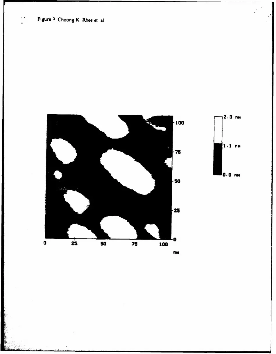
Figure 4 Choong K RKhee et al
2.3 nM100
S~1.1 nm
, 0.0 nu
710
no!
sou
25I

'igre 10 Choong K Rhee et. al
"AIf I SI I I
SpAI
°5 /
-1.2 -0.8 -0.4 0.0 0.4
Potential/V (vs. Ag/AgCl)

Figure I . Choong K RJie et &I.
300 . ' '
I..
-I 200
.. 100
0
-0.2 0.0 0.2 0.4 0.6
Potential/V (vs. Ag/AgCI)

9
Fi-lmr 12 oo tK Rhftea al.
300.0 not
,30.0
150. 0 no.
20.0 10.0 no
10.0
0 1o.o Ma md.ssOs
0 ~~~tO,.0. ~

Figure 13 ChcongK Riieeet 31
Etched Depth/nm
S
0o 0
0
0
0
0
00
4Ž


