Embed Size (px)
Citation preview

162
3D-nanoarchitectured Pd/Ni catalysts prepared byatomic layer deposition for the electrooxidation
of formic acidLoïc Assaud1, Evans Monyoncho2, Kristina Pitzschel1, Anis Allagui2,
Matthieu Petit1, Margrit Hanbücken1, Elena A. Baranova*2
and Lionel Santinacci*1
Full Research Paper Open Access
Address:1Aix-Marseille Université, CNRS, CINaM UMR 7325, 13288,Marseille, France and 2Department of Chemical and BiologicalEngineering, Center for Catalysis Research and Innovation, Universityof Ottawa, 161 Louis-Pasteur St., Ottawa, ON, K1N 6N5, Canada
Email:Elena A. Baranova* - [email protected];Lionel Santinacci* - [email protected]
* Corresponding author
Keywords:anodic aluminum oxide; atomic layer deposition (ALD); direct formicacid fuel cells; electrooxidation; nanostructured catalysts; Pd/Ni
Beilstein J. Nanotechnol. 2014, 5, 162–172.doi:10.3762/bjnano.5.16
Received: 30 September 2013Accepted: 14 January 2014Published: 12 February 2014
This article is part of the Thematic Series "Energy conversion applicationsof atomic layer deposition".
Guest Editor: J. Bachmann
© 2014 Assaud et al; licensee Beilstein-Institut.License and terms: see end of document.
AbstractThree-dimensionally (3D) nanoarchitectured palladium/nickel (Pd/Ni) catalysts, which were prepared by atomic layer deposition
(ALD) on high-aspect-ratio nanoporous alumina templates are investigated with regard to the electrooxidation of formic acid in an
acidic medium (0.5 M H2SO4). Both deposition processes, Ni and Pd, with various mass content ratios have been continuously
monitored by using a quartz crystal microbalance. The morphology of the Pd/Ni systems has been studied by electron microscopy
and shows a homogeneous deposition of granularly structured Pd onto the Ni substrate. X-ray diffraction analysis performed on Ni
and NiO substrates revealed an amorphous structure, while the Pd coating crystallized into a fcc lattice with a preferential orienta-
tion along the [220]-direction. Surface chemistry analysis by X-ray photoelectron spectroscopy showed both metallic and oxide
contributions for the Ni and Pd deposits. Cyclic voltammetry of the Pd/Ni nanocatalysts revealed that the electrooxidation of
HCOOH proceeds through the direct dehydrogenation mechanism with the formation of active intermediates. High catalytic activi-
ties are measured for low masses of Pd coatings that were generated by a low number of ALD cycles, probably because of the
cluster size effect, electronic interactions between Pd and Ni, or diffusion effects.
162
Beilstein J. Nanotechnol. 2014, 5, 162–172.
163
IntroductionOver the last decade, the miniaturization of fuel cells for the fast
expanding market of portable devices has become a chal-
lenging research topic. Direct formic acid fuel cell (DFAFC)
systems as electrochemical power sources have many advan-
tages such as the low-toxicity, unlike methanol, the low cost,
and the low fuel crossover at a high power density [1-3]. Palla-
dium is a good candidate to catalyze the electrooxidation of
formic acid thanks to its good stability at low pH and its high
activity [4-8]. The electrooxidation of HCOOH on Pd results in
the formation of CO2 and protons [7], which is a direct dehy-
drogenation pathway through the formation of active intermedi-
ates without the generation of poisonous CO species
(Scheme 1).
Scheme 1: Pd-catalyzed electrooxidation of HCOOH on Pd surfaces.
Despite the advantages of Pd catalysts for the electrooxidation
of formic acid, the activity is still not satisfactory enough for
commercial applications and more importantly, Pd tends to
dissolve and deactivate quickly by the impurities present in the
electrolyte [9]. Additionally, reducing the noble metal loading
by alloying Pd with a second cheap transition metal is essential
for a viable development of DFAFCs. In recent studies, several
metals such as Cu, Ni, Fe or Pt alloyed with Pd have been tested
[10-13] for the electrooxidation reaction of HCOOH, and have
shown a significant increase of the catalytic activity when
compared to pure Pd. Amongst them, the Pd/Ni bimetallic
system has shown very promising results due to the favorable
electronic effects that Ni brings into the system.
It is also well-known that decreasing the size of the active parti-
cles and thus increasing the electro-active surface area of the
catalyst are interesting ways to improve the electrooxidation of
HCOOH. Nanostructured substrates such as nanowires,
nanorods, nanopores or nanotubes have thus been investigated
to enhance the catalytic efficiency and to reduce the costs [14].
On the other hand, the physical, chemical and electrochemical
properties of the nanostructures are highly correlated with the
technique of fabrication. Among the numerous methods that
have been recently explored, the use of atomic layer deposition
(ALD) to fabricate and/or functionalize nanostructures appears
to be very promising. Catalysts grown by ALD often demon-
strated similar or enhanced properties as compared to those
grown by conventional methods, such as impregnation, ion-
exchange, and deposition–precipitation [15,16]. ALD has
initially been used to produce oxide layers to support the cata-
lysts [17], but two additional approaches have been recently
proposed: ALD is either used to grow metallic clusters or it is
applied to protect those metallic clusters with an ultrathin metal
oxide layer (see, e.g., the reviews [18-20]). This deposition
method is particularly interesting for electrocatalysis because it
allows an accurate control of both growth rate and composition
of the catalyst, and it provides a high coverage of high aspect
ratio nanostructures [21-23]. It is therefore possible to precisely
design catalysts onto nanoarchitectured supports that exhibit
enhanced abilities for fuel cell applications [24,25].
As previously proposed [26], nanoporous anodic aluminum
oxide (AAO) has been used as nanostructured support for the
Pd catalysts. The AAO membranes are attractive because they
exhibit a high specific surface area and the pore diameter and
length can be tailored easily [27,28]. In this study, the usual
two-step anodization process shown in Figure 1a–e, has been
used to grow well-ordered porous structures. Ni and Pd are then
successively deposited into the templates by ALD. The alumina
membranes are firstly coated by NiO that is reduced to metallic
Ni by annealing under H2 atmosphere [29,30] (Figure 1f). The
Pd clusters are then deposited directly onto the Ni films
(Figure 1g). Both NiO and Pd deposition processes have been
monitored by quartz crystal microbalance (QCM). The
morphology, the chemical composition and the crystalline struc-
tures have been investigated by scanning and transmission elec-
tron microscopy (SEM and TEM) and atomic force microscopy
(AFM), X-ray photoelectron spectroscopy (XPS) and X-ray
diffraction (XRD), respectively. The electrocatalytic activity of
the Pd/Ni systems, which were deposited on three-dimensional
alumina membranes with various mass content ratios, for the
electrooxidation of formic acid in acidic solution has been
studied by cyclic voltammetry (CV).
Results and DiscussionNickel depositionSince ALD processes have been developed mainly for metal
oxide and nitride thin films, metal depositions have been
hampered mostly by the lack of relevant and stable precursors
[31]. Although a new class of precursors that facilitates the
direct metal deposition, has recently been proposed [32], several
metals are often grown through a two-step process: (i) deposi-
tion of the metallic oxide and (ii) subsequent reduction (see,
e.g., [29,30]). Metallic Ni is therefore grown by using such an
approach [33,34]: the deposition of NiO is carried out from
nickelocene (NiCp2) and O3 precursors and the reduction of this
oxide film to metallic Ni is obtained by a reductive annealing
process under H2 atmosphere. The relative mass, m, gain and
loss have been monitored during the process by QCM and are
plotted in Figure 2a. A regular cyclic variation of the mass vs

Beilstein J. Nanotechnol. 2014, 5, 162–172.
164
Figure 1: Schematic description of the anodic alumina template fabrication and successive functionalization. (a) Initial Al disc, (b) electropolished Aldisc, (c) anodic Al2O3 porous layer, (d) pre-ordered Al disc after removal of the AAO sacrificial layer, (e) self-ordered AAO membrane, (f) Ni/NiO filmdeposited by ALD and reduced by annealing post treatment, (g) Pd cluster layer grown by ALD.
the number of ALD cycles is observed with an overall linear
evolution, which is typical for an ALD process with constant
growth rate. An enlarged view of one cycle presented in
Figure 2b shows in detail the process during the four succes-
sive steps of the NiO ALD sequence. The QCM measurements
indicate that the exposure and purging duration are optimized
for both NiCp2 and O3 pulses. The mass variations are indeed
reaching a plateau at the end of the exposure and purging
stages. After the short NiCp2 pulse (green period on the far
left of Figure 2b), the mass increases progressively up to a
maximum (Δm1) during the exposure phase (S1). Then a mass
loss is measured during the purging phase (S2). A similar trend
is observed after the O3 pulse: a mass increase (Δm2) is
measured during the exposure time (S3) followed by a total
mass loss during the purging phase (S4).
It is difficult to correlate the mass gain and loss measured by the
QCM with a reaction mechanism. Thus few data can be found
in literature about such chemical processes. However,
Martinson et al. proposed a detailed investigation of the Fe2O3
formation from FeCp2 and O3 precursors by using quadrupole
mass spectrometry (QMS) [35]. Since the precursors used for
this deposition are close to those employed in the present study,
the Martinson mechanism may be adapted to the deposition of
NiO using NiCp2 and O3. Therefore, the S1 period could be
ascribed to the adsorption of NiCp2 on the whole surface, which
after reaction on the active sites yields a –NiCp group on the
surface and one cyclopentadiene molecule is released. Note that
Martinson et al. have also detected cyclopentadione as a
byproduct in the ferrocene process. During the S2 stage, the
Figure 2: (a) In situ QCM measurement of the NiO mass gain duringthe ALD process. (b) Enlarged view of the mass gain for one ALDcycle. Δm corresponds to the net mass increase after the ALD cycle.
desorption of the precursors that have not reacted with active
surface sites seems to occur. The net mass gain detected after
the nickelocene pulse, exposure and purging could be attributed
to the bonding of a –NiCp group with a surface –OH group.
According to the study performed on Fe2O3 [35], the S3 and S4
stages could be associated to a combustion of the chemisorbed
–NiCp groups. Those cyclopentadienyl groups should therefore
be cracked with the production of CO2 and H2O. The surface is
then activated again with hydroxyl functions onto the Ni atoms.
While a mass loss, corresponding to the combustion of Cp, is
expected after the O3 exposure, the QCM measurements
(Figure 2b) do not show any net mass decrease during the step.

Beilstein J. Nanotechnol. 2014, 5, 162–172.
165
This unexpected measurement could be attributed to a cooling
effect of the vector gas (Ar) on the quartz. The QCM is indeed a
very sensitive characterization tool as the sensor oscillation
frequency can easily change when low temperature variations
occur. Additional experiments have thus been performed by
pulsing only ozone. Without NiCp2, the QCM data exhibit a
low level background and no regular increase. This indicates
that the general trends of m vs t shown in Figure 2a are relevant
but no mechanistic information can be deduced from the
detailed interpretation of the QCM measurements. QMS investi-
gation would be required to support the proposed chemical
mechanism.
In order to characterize their morphology, the resulting NiO/Ni
layers have been studied by electron microscopy. The backscat-
tering electron detection mode was used to enhance the chem-
ical contrast of the image shown in Figure 3. The NiO deposit
(red color in the figure) is clearly visible within the Al2O3
pores. The NiO film is approximately 10 nm thick after 1000
ALD cycles. The TEM picture presented in Figure 4 shows the
as-grown NiO layer deposited within the AAO membrane after
removal of the alumina template. The average length of the
nanotubes is 5 μm, which indicates that the exposure time to
NiCp2 is sufficiently long to allow for the deposition to proceed
deeply on the entire surface of the pores. On such a TEM
image, several NiO nanotubes can be observed. The NiO layer
covers the AAO template homogeneously. Note that no gradient
of NiO loading is observed in the deep section of the template.
The quantity of matter is identical at the top and the at the
bottom of the pores. This is attributed to the self-limiting
process of the ALD. The tuning of the duration of the surface
exposition to the precursors allows for the reaction of the mole-
cules with the activated surface of the three-dimensional
substrates, which exhibit a high aspect-ratio geometry.
The TEM image shows that the morphology of the NiO deposit
is highly granular. It therefore increases the active surface area
of the electrode for a higher interaction with the electrolyte.
Note that the NiO layer is an efficient barrier between the solu-
tion and the AAO since we have never observed the dissolution
of the AAO during the electrochemical characterizations. To get
a metallic Ni film, the as-grown NiO deposit has been annealed
in H2 atmosphere at 300 °C. The SEM observations indicate no
significant morphological modifications of the Ni after the
reductive annealing (Figure 5). The NiO film shown in Figure 3
(before annealing) exhibits a granularity slightly higher than in
Figure 5 (after annealing). It is however difficult to get quanti-
tative results from such SEM pictures. Note that inversely, a
treatment performed in Ar at higher temperature (T = 700 °C)
has shown a strong increase of the granularity after such
annealing [34].
Figure 3: (a) SEM cross section of a NiO layer deposited in AAOmembrane. (b) SEM image (obtained in backscattering electron mode)showing NiO grown by ALD within the AAO template. The NiO toplayer has been removed by a short Ar sputtering in order to reveal theNiO film coating the vertical pore walls. The NiO deposit is empha-sized on the picture using a red overlay.
Figure 4: (a) TEM image of NiO nanotubes after alumina templateremoval. (b) Enlarged view of NiO nanotubes.
Figure 5: SEM image of Ni layer deposited in an AAO template after3 h annealing in H2 at 300 °C of the initially deposited NiO by ALD.The inset shows a detailed top-view of the surface.

Beilstein J. Nanotechnol. 2014, 5, 162–172.
166
Figure 7: ALD sequence during Pd deposition from Pd(hfac)2 and formaldehyde.
Figure 6: XPS survey spectrum of metallic Ni.
The chemical composition as well as the crystal structure of the
NiO/Ni layer have been analyzed before and after the reduction
stage. The XRD analyses performed on as-grown NiO and after
the reduction process indicate that both NiO and Ni layers
deposited on AAO are amorphous (XRD patterns are shown in
Figure S1, Supporting Information File 1). The surface chem-
istry of the sample after the reductive annealing of the Ni
deposit has been analyzed by XPS. As expected, the spectrum
shown in Figure 6 exhibits peaks corresponding to Ni, C and Si
but also to O. Although the Ni 2p, Ni 3p and Auger peaks indi-
cate the presence of metallic Ni, the O 1s peak suggests that the
Ni deposit remains partially oxidized after the reductive treat-
ment. Since the XPS analysis provides information on the outer-
most surface, the Ni–O contribution can either originate from an
only partial reduction of the initial NiO layer or from the oxi-
dation of the sample while transferring it to the XPS chamber.
Note that a contribution coming from SiO2 in the XPS spec-
trum in the O 1s binding energies region is possible since an
interfacial SiO2 layer is formed between Si and NiO (Figure S2,
Supporting Information File 1). However, the contribution of Si
in the survey spectrum is not intense.
Palladium depositionA key advantage of ALD is that the growth of materials
proceeds according to a two-dimensional mechanism. Neverthe-
less, for electrocatalytic applications, it is more suitable to have
metallic clusters. To obtain such a morphology, it is possible to
adjust the deposition parameters and the nature of the precursor.
The outcome will depend also on the interaction between the
substrate and the deposit. Recently, Elam et al. [25] have
reported the synthesis of sub-nanometer Pd particles by an alter-
nating exposure of the substrate to the metallic precursor and to
trimethylaluminum. The active hydroxyl sites are thus occu-
pied, which hinders the lateral growth of the particles. As
mentioned in the introduction, the growth of Pd clusters by a
direct ALD process, which uses palladium hexafluoroacetylace-
tone (Pd(hfac)2) and formaldehyde, has been previously
described [25,36-38]. The mechanism is summarized in
Figure 7. Steps 1 and 2 consist of the adsorption of the
Pd(hfac)2 precursor onto the surface and its reaction with the
hydroxyl sites and a subsequent H-hfac release. After the expo-
sition of the surface to the second precursor (step 3), Pd(hfac) is
reduced by formaldehyde. A –Pd–Hx termination is created at
the active site and Hhfac, CO and H2 are released during step 4.
The formation process of the Pd clusters has been monitored by
QCM measurements in order to detect the mass gain and loss
during the ALD cycles. The general evolution of m during the
deposition is shown in Figure 8a. Two growth regimes are iden-
tified in the curve: before and after 50 cycles. At first, the
growth rate of Pd is low and non-linear. It progressively
increases and reaches an almost linear growth after 50 ALD
cycles. Such behavior has already been observed [36,39]. The
initial low growth rate has been attributed to the long nucle-
ation stage of the Pd clusters onto oxidized surfaces and/or

Beilstein J. Nanotechnol. 2014, 5, 162–172.
167
Figure 9: SEM top views of Pd deposits after 100 ALD cycles onto (a) as-grown NiO and (b) reduced NiO films on Si substrate. (c) AFM image of Pdclusters onto as-grown ALD NiO.
Figure 8: In situ QCM measurements of Pd mass gain during the ALDprocess for Pd. (a) General evolution and (b) enlarged view of oneALD cycle.
ascribed to the surface poisoning by the precursor ligands by
others [38]. An enlarged view on one ALD cycle (Figure 8b)
shows the details of the mass gain and loss during the precursor
pulses and the pumping of the exposition chamber. Step S1
consists of the adsorption of Pd(hfac)2 precursor molecules onto
the surface. At this stage, the mass gain is denoted Δm1. The
end of the exposure time (S1) does not correspond exactly to
the maximum of the gain mass Δm1. The exposure time could
thus be decreased to optimize the cycle duration. However, a
long exposure duration assures the diffusion of the chemical
species toward the pore tips. A similar observation can be done
for the pumping time (step S2). Its duration is also not opti-
mized but a longer purge and pumping stage would surely
remove all the byproducts and the excess of reactants. George et
al. [38] have shown that during the exposure with Pd(hfac)2, the
released Hhfac can adsorb onto the hydroxylated Ni surface and
block any further Pd reaction at those locations. As mentioned
above, this phenomenon can hinder the lateral growth of the Pd
film and slows down the deposition rate at the beginning. Steps
S3 and S4 describe the surface exposure to the second precursor
(formaldehyde) and the purge/pumping of the reactor, respect-
ively. At the end of second part of the ALD cycle, the net mass
variation should be negative. After the reaction of HCOH with
–Ni–O–Pd(hfac), H-hfac, CO and H2 are indeed released.
However, the QCM measurements show no mass loss. This
unexpected measurement could again be attributed to the
cooling effect of the vector gas on the quartz oscillation that has
been mentioned above for Ni deposition. These data give only
an indication on the general deposition process and cannot be
used to interpret the growth mechanism. QCM data indicate that
Pd deposition takes place onto the surface since the general
trend is almost flat if no Pd is pulsed in the chamber.
The morphologies of the Pd films grown onto the NiO layer
have been observed by SEM and AFM with and without the
reductive annealing treatment in H2. In order to facilitate such
characterizations, the observed NiO and Pd layers have been
grown onto flat Si substrates. Note that these depositions onto
planar Si and onto AAO membranes have been performed
simultaneously. Pd deposits carried out onto as-grown and
annealed NiO layers that were grown before onto the Si wafers
are presented in Figure 9a and Figure 9b, respectively. Their
average diameters are, respectively, about 40 and 10–20 nm.
The size of the clusters observed in Figure 9a cannot be attrib-
uted to the supporting NiO crystallites since their average size is
in the range of 10–15 nm according to TEM cross section
shown as supplemental material (Figure S2, Supporting Infor-
mation File 1). The QCM, XPS and XRD measurements also
attest the deposition of Pd onto the NiO layers. Such a spher-
Beilstein J. Nanotechnol. 2014, 5, 162–172.
168
ical morphology suggests a Volmer–Weber growth mechanism
of Pd. Such a formation of 3D islands is due to the high differ-
ence of surface energies between the metallic Pd and the
oxidized support [39,40]. The formation of 3D islands can also
be supported by the H-hfac ligands that are adsorbed on active
–OH sites at the surface after the Pd(hfac)2 pulse [38]. In the
case of Figure 9b, it was more difficult to observe the clusters
with a high resolution. However the average size is slightly
higher than the initial Ni/NiO layer. It indicates therefore that
the Pd deposit covers the Ni/NiO film uniformly. This could be
due to a lower surface energy between the Pd and the annealed
substrate. It is even possible to form a Pd/Ni alloy if the NiO
top layer appears only when the sample is exposed to air.
The two different growth mechanisms demonstrate the strong
influence of the substrate on the deposition process. Although
the XPS data indicate that the reduction of NiO to Ni is not
total, the Pd deposition proceeds according to a 2D growth
mechanism after the annealing in H2 atmosphere. In order to
optimize the catalyst morphology, it appears that the Pd deposi-
tion should be performed onto as-grown NiO because bigger Pd
islands are formed then. The AFM image presented in
Figure 9c, shows clearly the Pd clusters that cover all of the Ni/
NiO layer surface. Since Figure 9a and Figure 9b show planar
substrates, they cannot be used to precisely evaluate the size of
the Pd particles in the NiO/AAO system. However they give
valuable information about the nucleation process of the Pd
clusters on the NiO and Ni surfaces. Since atomic layer deposi-
tion is a self-limiting layer-by-layer process, it is reasonable to
assume that the deposition occurs within the AAO/NiO struc-
tures but the particle size should be lower than the one observed
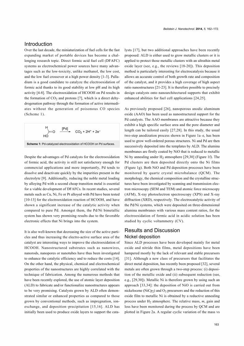
on planar substrate. The crystal structure of Pd deposit has been
investigated by X-ray diffraction. The XRD patterns shown in
Figure 10 depict a polycrystalline structure of the Pd layer with
a preferential orientation in the [220] direction (peak at about
70°). The Pd crystallographic structure is face centred cubic
(fcc) similar to the structure of bulk Pd metal [11]. The XRD
diffractogram suggests therefore the presence of metallic Pd.
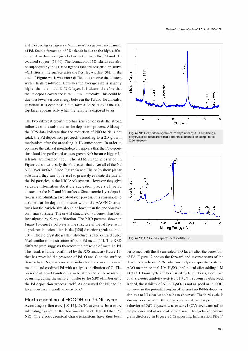
This result is further confirmed by the XPS analysis (Figure 11)
that has revealed the presence of Pd, O and C on the surface.
Similarly to Ni, the spectrum indicates the contribution of
metallic and oxidized Pd with a slight contribution of O. The
presence of Pd–O bonds can also be attributed to the oxidation
occurring during the sample transfer to the XPS chamber or to
the Pd deposition process itself. As observed for Ni, the Pd
layer contains a small amount of C.
Electrooxidation of HCOOH on Pd/Ni layersAccording to literature [10-13], Pd/Ni seems to be a more
interesting system for the electrooxidation of HCOOH than Pd/
NiO. The electrochemical characterizations have thus been
Figure 10: X-ray diffractogram of Pd deposited by ALD exhibiting apolycrystalline structure with a preferential orientation along the fcc[220] direction.
Figure 11: XPS survey spectrum of metallic Pd.
performed with the H2-annealed NiO layers after the deposition
of Pd. Figure 12 shows the forward and reverse scans of the
third CV cycle on Pd/Ni electrocatalysts deposited onto an
AAO membrane in 0.5 M H2SO4 before and after adding 1 M
HCOOH. From cycle number 1 until cycle number 3, a decrease
of the electrocatalytic activity of Pd/Ni system is observed.
Indeed, the stability of Ni in H2SO4 is not as good as in KOH,
however in the potential region of interest no Pd/Ni deactiva-
tion due to Ni dissolution has been observed. The third cycle is
shown because after three cycles a stable and reproducible
behavior of Pd/Ni system was obtained (CVs are identical) in
the presence and absence of formic acid. The cyclic voltammo-
gram disclosed in Figure S3 (Supporting Information File 1)

Beilstein J. Nanotechnol. 2014, 5, 162–172.
169
Figure 12: Cyclic voltammograms of Pd(100 ALD cycles)/Ni(1000 ALDcycles) catalysts in 0.5 M H2SO4 without (blue dashed line) and with(continuous green line) 1 M HCOOH at 15 mV·s−1. Current densitiesare given per unit mass of Pd estimated from the QCM measurements.
shows the evolution of the current during the first six cycles. It
demonstrates the stability of the Pd/Ni system over time in
0.5 M H2SO4.
The Ni and Pd layers were formed after 1000 and 100 ALD
cycles, respectively, on alumina membranes. The applied poten-
tial varies from −0.75 to 0.4 V vs MSE at 15 mV·s−1. At poten-
tials lower than −0.6 V, the H2 adsorption/desorption process is
observed. Without formic acid in the solution, at potentials
between −0.6 and 0 V, the voltammogram exhibits a flat region
till approximately 0 V and at higher potentials the formation of
Pd oxides starts to take place. In the presence of formic acid, on
the other hand, the current begins to increase at a potential of
−0.58 V reaching a maximum current density of 0.26 A·mg−1 at
−0.2 V because of the oxidation of HCOOH. A further increase
of the potential leads to a decrease of the current density due to
the oxidation of the palladium and the inhibition of the catalytic
activity of the metallic system by reaction intermediates [9,41].
On the reverse scan, the current remains low until 0.19 V, at
which the reduction of PdOx begins to take place, and then
increases because of the electrooxidation of formic acid on the
reduced Pd. Note that the anodic wave that is centered at
−0.19 V in the reverse scan is slightly higher than the one
during the forward scan. This hysteresis indicates that the Pd
surface still remains active and the previously formed oxides
are completely reduced when the potential is reversed toward
the negative direction. The electrooxidation of HCOOH follows
the direct dehydrogenation pathway, which is in agreement with
previous works [42]. The effect of the number of Pd ALD
cycles (40, 80, 100 and 145) and, consequently, the Pd to Ni
ratio on the current peak at −0.19 V, which corresponds to the
oxidation of HCOOH is shown in Figure 13. Additionally, the
electrochemical characterizations have shown the typical Pd
response in H2SO4. The obtained results (overpotential for the
oxidation of formic acid) are in a good agreement with the
literature data reported for Pd/transition metal systems prepared
by other techniques [10,13].
Figure 13: Peak current densities of the electrooxidation of 1 MHCOOH in 0.5 M H2SO4 with various Pd contents in the Pd/Ninanocatalysts, which were obtained with 40 to 145 Pd ALD cycles. Themass of Pd was estimated from the QCM measurements.
The mass activity of the Pd systems decreases to about one
fourth from 40 to 145 ALD cycles. The increase of mass of Pd
may result in the formation of larger clusters, and subsequently
in both a smaller overall active surface area of the catalyst per
unit mass, and weaker interactions with the Ni support. These
two reasons can explain the negative trend of peak current
densities for the oxidation of formic acid on Pd/Ni electrocata-
lysts with the increase of Pd mass. Note that it can also be
because of the mass transport effect [43] since diffusion into
such narrow channels can differ strongly from standard 2D
models.
ConclusionIn this study, well-defined Pd/Ni nanocatalysts grown by ALD
have been investigated for the electrooxidation of formic acid in
0.5 M H2SO4. The deposition of nickel oxide from NiCp2 and
O3 precursors on high aspect ratio nanoporous Al2O3 has been
demonstrated. Although the chemical composition analysis of
the NiO layers has not shown that the reductive treatment in H2
leads to fully metallic films, in which no strong morphological
modifications were observed. Furthermore, it was concluded
that the oxidized Ni is a better substrate to obtain a three-dimen-
sional growth of Pd islands, which are more suitable for electro-
catalytic applications. The Pd deposit is polycrystalline and
exhibits a preferential orientation along the [220] direction. For

Beilstein J. Nanotechnol. 2014, 5, 162–172.
170
both Ni and Pd depositions, the QCM results were not conclu-
sive with regard to proper information about the deposition
mechanisms by ALD. The Pd/Ni bimetallic systems demon-
strates a high activity toward the electrooxidation reaction of
formic acid and reaches 0.83 A·mg−1 for Pd(40 ALD cycles)/
Ni(1000 ALD cycles). The electrochemical properties are very
similar to those reported in the literature [10-13]. The inter-
action between Pd and Ni is stronger when the mass of the
deposited Pd is decreased because of the lower thickness and
size of Pd particles, but also because of the electronic effects
between the alloyed Pd/Ni metals or because of the mass trans-
port effect in 3D nanostructures. This explains the trend of
higher peak current densities for the electrooxidation of formic
acid at a lower Pd content in the Pd/Ni nanocatalysts.
ExperimentalThe porous alumina structures have been grown on 4 cm wide
aluminum discs (Goodfellow, 99.999%) by using the method
that is schematically depicted in Figure 1a–e. The aluminum
was first electropolished in an alcoholic solution of perchloric
acid and successively anodized at a constant voltage, U, of 40 V
in oxalic acid. A chemical dissolution was performed between
the two anodizations to remove the disordered sacrificial Al2O3
layer. The resulting alumina membrane is ordered on a large
scale area (ca. 10 cm2); the pore diameter is 40 nm and the
length of the pores is about 5 μm. A typical AAO template is
shown in Figure 14.
Figure 14: SEM micrograph of an anodic alumina oxide template.After the electropolishing, a sacrificial film was firstly grown by applying40 V in 0.3 M H2C2O4 for 24 h at T = 8 °C and then dissolved inH2CrO4 and H3PO4 at 50 °C for 12 h. The second anodization step isthen carried out during 2.5 h at the same anodic conditions.
The Pd/Ni catalysts have been prepared by ALD in a Fiji 200
reactor from Ultratech/Cambridge Nanotech. The catalysts (Ni
and Pd) were deposited both on AAO membranes and on flat
Si(100) wafers that were cleaned beforehand by sonication in
acetone, isopropanol and ethanol and deoxidized by dipping in
1% HF for 5 s. The alumina template was coated by a thin NiO
layer grown from nickelocene (NiCp2, 99% from STREM
chemicals), and ozone as chemical precursors. The temperature
of the ALD chamber during the deposition was set to 250 °C.
The ALD cycle consisted of successive exposures of the sample
to NiCp2 and O3. The pulse durations and exposure time were,
respectively, 1 and 30 s for NiCp2 and 0.2 and 20 s for O3. In
both cases, the purging of the chamber was carried out for 30 s.
The resulting NiO film was annealed and reduced under a H2
flow at 300 °C for 3 h to obtain a metallic Ni layer. The last step
of the preparation of the catalysts consisted of depositing
Pd nanoclusters that have been grown from palladium(II)
hexafluoroacetylacetonate (Pd(hfac)2, 98% from STREM
chemicals), and formalin (37% formaldehyde in water with
10–15% of methanol from Sigma-Aldrich) at 200 °C. The ALD
sequence consisted of successive exposures of the Ni-covered
sample to Pd(hfac)2 and formaldehyde. The pulse durations
were, respectively, 1 and 3 s. In both cases, the exposure and
purge durations were 30 s. Due to the low vapor pressure of the
Pd precursor, an argon flow has been injected in the canister for
0.25 s through an additional valve before each precursor pulse
in order to enhance the transport of chemical species toward the
deposition chamber. Experiments with various number of ALD
cycles of the different precursors have been performed to adjust
the mass and the composition of the films. A chemical etching
performed in chromic acid solution allows to chemically
dissolve the alumina template to allow for the nanostructured
catalysts to be collected by centrifugation for further TEM
observations of the catalysts out of the alumina template. The
Pd/Ni catalysts have been deposited both on 3D alumina
templates and flat Si(100) wafers in order to facilitate the chem-
ical and structural characterizations. In situ monitoring of the
relative mass gain and loss was performed by using a quartz
crystal microbalance (QCM from Inficon). The QCM is
connected to the ALD chamber and driven by a SQM-160
controller for data acquisition. The morphology of Al2O3
templates and Pd/Ni electrocatalysts has been observed by SEM
and TEM using, respectively, JEOL 6320-F and JEOL 3010
equipment. Some additional morphological investigations have
been carried out by non-contact AFM using a XE 100 micro-
scope from Park systems. The crystalline structure of NiO, Ni
and Pd has been characterized by X-ray diffraction using an
INEL diffractometer equipped with a quartz monochromator
and a horizontally disposed 1D curved position detector (CPS-
120) that covers a 2θ angle of 120°. The measurements were
obtained in reflection mode with an incident angle of 10° and
Cu Kα1 (1.54056 Å) radiation. X-ray photoelectron spec-
troscopy by using a Mg electrode Kα (1253.6 eV) source
(HA150 from VSW) was used for surface chemistry composi-
tion analysis. The Electrooxidation of HCOOH on alumina-
supported Pd/Ni catalysts after reductive annealing treatment of
Beilstein J. Nanotechnol. 2014, 5, 162–172.
171
the NiO ALD layer has been studied in 0.5 M H2SO4 solution
in a three-electrode teflon cell. A large surface area Pt mesh and
a mercury sulfate electrode (MSE) served respectively as
counter and reference electrodes. The geometric area of the
working electrode was 0.196 cm2. The electrical contact to the
working electrode was established by a gold wire on the Pd/Ni
layer. Cyclic voltammetry was carried out by using a BioLogic
VSP potentiostat together with the EC-Lab software at room
temperature. The CVs were performed in the potential region
from −0.75 to 0.4 V vs MSE at a scanning rate of 15 mV·s−1.
The current densities have been reported per unit mass of Pd
(details on the Pd mass calculations can be found in Supporting
Information File 1).
Supporting InformationSupporting Information File 1Additional experimental details
[http://www.beilstein-journals.org/bjnano/content/
supplementary/2190-4286-5-16-S1.pdf]
AcknowledgementsThe authors acknowledge Damien Chaudanson and Serge
Nitsche for their precious help with the electron microscopy,
Jean-Yves Hoarau for XPS analysis and Vasile Heresanu for
XRD measurements and interpretation. This work was
supported by the France Canada Research Fund. The European
Regional Development Fund (ERDF), the PACA Regional
Council, the French Ministry of Higher Education and Research
and the CNRS are also acknowledged for funding.
References1. Yu, X.; Pickup, P. G. J. Power Sources 2008, 182, 124–132.
doi:10.1016/j.jpowsour.2008.03.0752. Rice, C.; Ha, S.; Masel, R. I.; Wieckowski, A. J. Power Sources 2003,
115, 229–235. doi:10.1016/S0378-7753(03)00026-03. Rice, C.; Ha, S.; Masel, R. I.; Waszczuk, P.; Wieckowski, A.;
Barnard, T. J. Power Sources 2002, 111, 83–89.doi:10.1016/S0378-7753(02)00271-9
4. Liu, Z.; Hong, L.; Tham, M. P.; Lim, T. H.; Jiang, H. J. Power Sources2006, 161, 831–835. doi:10.1016/j.jpowsour.2006.05.052
5. Choi, J. H.; Noh, S. Y.; Han, S. D.; Yoon, S. K.; Lee, C.-S.;Hwang, T.-S.; Rhee, Y. W. Korean J. Chem. Eng. 2008, 25,1026–1030. doi:10.1007/s11814-008-0167-2
6. Antolini, E. Energy Environ. Sci. 2009, 2, 915–931.doi:10.1039/B820837A
7. Baik, S. M.; Han, J.; Kim, J.; Kwon, Y. Int. J. Hydrogen Energy 2011,36, 14719–14724. doi:10.1016/j.ijhydene.2011.04.181
8. Yang, L.; Su, H.; Shu, T.; Liao, S. Sci. China: Chem. 2012, 55,391–397. doi:10.1007/s11426-011-4485-6
9. Du, C.; Chen, M.; Wang, W.; Yin, G. ACS Appl. Mater. Interfaces 2011,3, 105–109. doi:10.1021/am100803d
10. Xu, C.; Liu, Y.; Wang, J.; Geng, H.; Qiu, H. J. Power Sources 2012,199, 124–131. doi:10.1016/j.jpowsour.2011.10.075
11. Shen, S. Y.; Zhao, T. S.; Xu, J. B.; Li, Y. S. J. Power Sources 2010,195, 1001–1006. doi:10.1016/j.jpowsour.2009.08.079
12. Baranova, E. A.; Miles, N.; Mercier, P. H. J.; Page, Y. L.;Patarachao, B. Electrochim. Acta 2010, 55, 8182–8188.doi:10.1016/j.electacta.2009.12.090
13. Hu, S.; Ha, S.; Scudiero, L. Electrochim. Acta 2013, 105, 362–370.doi:10.1016/j.electacta.2013.05.012
14. Zhong, C.-J.; Luo, J.; Fang, B.; Wanjala, B. N.; Njoki, P. N.;Loukrakpam, R.; Yin, J. Nanotechnology 2010, 21, 062001.doi:10.1088/0957-4484/21/6/062001
15. Feng, H.; Elam, J. W.; Libera, J. A.; Setthapun, W.; Stair, P. C.Chem. Mater. 2010, 22, 3133–3142. doi:10.1021/cm100061n
16. Lu, J.; Liu, B.; Greeley, J. P.; Feng, Z.; Libera, J. A.; Lei, Y.;Bedzyk, M. J.; Stair, P. C.; Elam, J. W. Chem. Mater. 2012, 24,2047–2055. doi:10.1021/cm300203s
17. Haukka, S.; Lakomaa, E. L.; Suntola, T. Adsorption controlledpreparation of heterogeneous catalysts. In Adsorption and itsApplications in Industry and Environmental Protection; Dabrowski, A.,Ed.; Studies in Surface Science and Catalysis, Vol. 120A; Elsevier:Amsterdam, 1999; pp 715–750.
18. Detavernier, C.; Dendooven, J.; Sree, S. P.; Ludwig, K. F.;Martens, J. A. Chem. Soc. Rev. 2011, 40, 5242–5253.doi:10.1039/c1cs15091j
19. Elam, J. W.; Dasgupta, N. P.; Prinz, F. B. MRS Bull. 2011, 36,899–906. doi:10.1557/mrs.2011.265
20. Lu, J.; Elam, J. W.; Stair, P. C. Acc. Chem. Res. 2013, 46, 1806–1815.doi:10.1021/ar300229c
21. Goldstein, D. N.; George, S. M. Appl. Phys. Lett. 2009, 95, 143106.doi:10.1063/1.3238558
22. Binder, A.; Seipenbusch, M. Appl. Catal., A 2011, 396, 1–7.doi:10.1016/j.apcata.2010.12.030
23. Liang, X.; Lyon, L. B.; Jiang, Y.-B.; Weimer, A. W. J. Nanopart. Res.2012, 14, No. 943. doi:10.1007/s11051-012-0943-0
24. Rikkinen, E.; Santasalo-Aarnio, A.; Airaksinen, S.; Borghei, M.;Viitanen, V.; Sainio, J.; Kauppinen, E. I.; Kallio, T.; Krause, A. O. I.J. Phys. Chem. C 2011, 115, 23067–23073. doi:10.1021/jp2083659
25. Feng, H.; Libera, J. A.; Stair, P. C.; Miller, J. T.; Elam, J. W. ACS Catal.2011, 1, 665–673. doi:10.1021/cs2000957
26. Chen, Y.-X.; Lavacchi, A.; Chen, S.-P.; di Benedetto, F.;Bevilacqua, M.; Bianchini, C.; Fornasiero, P.; Innocenti, M.; Marelli, M.;Oberhauser, W.; Sun, S.-G.; Vizza, F. Angew. Chem., Int. Ed. 2012,51, 8500–8504. doi:10.1002/anie.201203589
27. Moyen, E.; Santinacci, L.; Masson, L.; Sahaf, H.; Macé, M.; Assaud, L.;Hanbücken, M. Int. J. Nanotechnol. 2012, 9, 246–259.doi:10.1504/IJNT.2012.045330
28. Moyen, E.; Santinacci, L.; Masson, L.; Wulfhekel, W.; Hanbücken, M.Adv. Mater. 2012, 24, 5094–5098. doi:10.1002/adma.201200648
29. Rüffer, D.; Huber, R.; Berberich, P.; Albert, S.; Russo-Averchi, E.;Heiss, M.; Arbiol, J.; Fontcuberta i Morral, A.; Grundler, D. Nanoscale2012, 4, 4989–4995. doi:10.1039/c2nr31086d
30. Peck, M. A.; Langell, M. A. Chem. Mater. 2012, 24, 4483–4490.doi:10.1021/cm300739y
31. Miikkulainen, V.; Leskelä, M.; Ritala, M.; Puurunen, R. L. J. Appl. Phys.2013, 113, 021301. doi:10.1063/1.4757907
32. Lim, B. S.; Rahtu, A.; Gordon, R. G. Nat. Mater. 2003, 2, 749–754.doi:10.1038/nmat1000
33. Chae, J.; Park, H.-S.; Kang, S.-w. Electrochem. Solid-State Lett. 2002,5, C64–C66. doi:10.1149/1.1475199

Beilstein J. Nanotechnol. 2014, 5, 162–172.
172
34. Bachmann, J.; Zolotaryov, A.; Albrecht, O.; Goetze, S.; Berger, A.;Hesse, D.; Novikov, D.; Nielsch, K. Chem. Vap. Deposition 2011, 17,177–180. doi:10.1002/cvde.201004300
35. Martinson, A. B. F.; DeVries, M. J.; Libera, J. A.; Christensen, S. T.;Hupp, J. T.; Pellin, M. J.; Elam, J. W. J. Phys. Chem. C 2011, 115,4333–4339. doi:10.1021/jp110203x
36. Elam, J. W.; Zinovev, A.; Han, C. Y.; Wang, H. H.; Welp, U.;Hryn, J. N.; Pellin, M. J. Thin Solid Films 2006, 515, 1664–1673.doi:10.1016/j.tsf.2006.05.049
37. Stair, P. C. J. Chem. Phys. 2008, 128, 182507. doi:10.1063/1.282493938. Goldstein, D. N.; George, S. M. Thin Solid Films 2011, 519,
5339–5347. doi:10.1016/j.tsf.2011.02.03739. Weber, M. J.; Mackus, A. J. M.; Verheijen, M. A.; van der Marel, C.;
Kessels, W. M. M. Chem. Mater. 2012, 24, 2973–2977.doi:10.1021/cm301206e
40. Campbell, C. T. Surf. Sci. Rep. 1997, 27, 1–111.doi:10.1016/S0167-5729(96)00011-8
41. Capon, A.; Parsons, R. J. Electroanal. Chem. 1975, 65, 285–305.doi:10.1016/0368-1874(75)85124-0
42. Li, R.; Wei, Z.; Huang, T.; Yu, A. Electrochim. Acta 2011, 56,6860–6865. doi:10.1016/j.electacta.2011.05.097
43. Lindström, R. W.; Seidel, Y. E.; Jusys, Z.; Gustavsson, M.;Wickman, B.; Kasemo, B.; Behm, R. J. J. Electroanal. Chem. 2010,644, 90–102. doi:10.1016/j.jelechem.2009.04.034
License and TermsThis is an Open Access article under the terms of the
Creative Commons Attribution License
(http://creativecommons.org/licenses/by/2.0), which
permits unrestricted use, distribution, and reproduction in
any medium, provided the original work is properly cited.
The license is subject to the Beilstein Journal of
Nanotechnology terms and conditions:
(http://www.beilstein-journals.org/bjnano)
The definitive version of this article is the electronic one
which can be found at:
doi:10.3762/bjnano.5.16


![[PD] Libros - Mapas Estrategicos](https://img.dokumen.tips/doc/110x75/6359494c341e5cd74a0a96c8/pd-libros-mapas-estrategicos.jpg)