Embed Size (px)
Citation preview

IEEE TRANSACTIONS ON PLASMA SCIENCE, VOL. 43, NO. 4, APRIL 2015 951
Efficiencies of Aloof-Scattered Electron BeamExcitation of Metal and Graphene Plasmons
Kelvin J. A. Ooi, Member, IEEE, Wee Shing Koh, Senior Member, IEEE, Hong Son Chu,Dawn T. H. Tan, and Lay Kee Ang, Senior Member, IEEE
Abstract— We assessed the efficiencies of surface plasmonexcitation by an aloof-scattered electron beam on metals andgraphene. Graphene is shown to exhibit high energy transferefficiencies at very low electron kinetic energy requirements.We show that the exceptional performance of graphene is due toits unique plasmon dispersion, low electronic density, and thin-film structure. The potential applications of these aloof-scatteredgraphene plasmons are discussed in the aspects of coherentradiation.
Index Terms— Electron beams, graphene, slow light, surfaceplasmons (SPs).
I. INTRODUCTION
THE interaction of swift electrons with matter providespathways for evanescent sources of light [1]. One of these
pathways involves the excitation of surface plasmons (SPs),which is usually generated by bombardment of swift electronsonto a thin metal film, as has been shown in [2]. Anothermethod to excite SPs is the aloof scattering of electrons, whichwas demonstrated in [3], whereby the electron trajectory doesnot intersect the metal, as schematically shown in Fig. 1.This method involves low energy transfer and thus minimizessample damage, in addition to opening up other interestingradiation pathways, such as the plasmon-controlled Cherenkovradiation as has been recently shown in [4].
The aloof scattering of electrons to excite plasmons onmetals is well studied in the field of electron-loss spec-troscopy [1], both in theoretical formulation and experimentalobservation. In this paper, however, we want to study the aloof
Manuscript received July 4, 2014; revised October 28, 2014; acceptedDecember 1, 2014. Date of publication December 18, 2014; date of currentversion April 13, 2015. This work was supported in part by the SingaporeUniversity of Technology and Design (SUTD)-MIT International DesignCentre under Grant IDD21200103 and Grant IDG21200106 and in partby the SUTD under Grant SRG EPD 2011014. The work of H. S. Chuwas supported by the National Research Foundation, Singapore, within theCompetitive Research Programme under Grant NRF-CRP 8-2011-07. Thework of L. K. Ang was supported by the U.S. Air Force Office of ScientificResearch through the Asian Office of Aerospace Research and Developmentunder Grant 14-4020.
K. J. A. Ooi, D. T. H. Tan, and L. K. Ang are with the EngineeringProduct Development, Singapore University of Technology and Design,Singapore 138682 (e-mail: [email protected]; [email protected];[email protected]).
W. S. Koh and H. S. Chu are with the Department of Electronics andPhotonics, Institute of High Performance Computing, Agency forScience, Technology and Research, Singapore 138632 (e-mail:[email protected]; [email protected]).
Color versions of one or more of the figures in this paper are availableonline at http://ieeexplore.ieee.org.
Digital Object Identifier 10.1109/TPS.2014.2379259
Fig. 1. Aloof scattering of an electron on a metal/graphene sheet. The electronmoves with velocity, v, above the sheet with impact parameter, z. The sheethas a thickness of �.
scattering of electrons on graphene, which is still a relativelynew area of research with potentially exciting new physics [5].
II. CONDITIONS FOR ALOOF-SCATTERING
EXCITATION OF SURFACE PLASMONS
An aloof-scattered electron can favorably couple to SPpolaritons (SPPs) of propagation constant given by ksp = ω/v,where ω is the radian frequency and v is the velocity of theelectron. As such, the velocity and hence kinetic energy ofthe electron required to excite SPPs are greatly dictated bythe plasmon dispersion of the metal. The plasmon dispersionrelation for odd SPP modes on a metal of finite thickness isgiven by the following [6]:
coth
(√k2
sp − ω2μ0ε0εm�
2
)= −εm
εd·
√k2
sp − ω2μ0ε0εd√k2
sp − ω2μ0ε0εm
(1)
where εm = ε∞ − ω2p/[ω(ω + iγ )] is the metal permittivity,
ωp is the plasma frequency, ε∞ is the high-frequency dielectricconstant of the metal, and γ is the relaxation frequency. εd isthe dielectric background permittivity, ε0 is the free spacepermittivity, μ0 is the free space permeability, and � is themetal thickness.
A. SPP Excitation on Bulk Metals
For bulk metals, we can approximate the system to be aninfinite half space by taking lim(� → ∞) in (1). This bringsus to the result of the commonly seen dispersion relation
ksp = ω
c
√εdεm
εd + εm(2)
0093-3813 © 2014 IEEE. Personal use is permitted, but republication/redistribution requires IEEE permission.See http://www.ieee.org/publications_standards/publications/rights/index.html for more information.
952 IEEE TRANSACTIONS ON PLASMA SCIENCE, VOL. 43, NO. 4, APRIL 2015
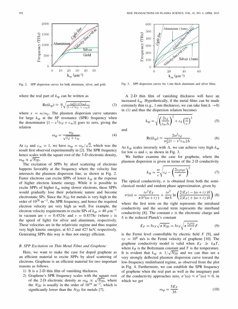
Fig. 2. SPP dispersion curves for bulk aluminum, silver, and gold.
where the real part of ksp can be written as
Re(ksp) ≈ ωc
√εd (1−x2ε∞)
[1−x2(εd + ε∞)] (3)
where x = ω/ωp . The plasmon dispersion curve saturatesfor large ksp at the SP resonance (SPR) frequency whenthe denominator [1 − x2(εd + ε∞)] goes to zero, giving therelation
ωsp = ωp√εd + ε∞
. (4)
At εd and ε∞ = 1, we have ωsp = ωp/√
2, which was theresult first observed experimentally in [2]. The SPR frequencyhence scales with the square root of the 3-D electronic density,ωsp ∝ √
N3D.The excitation of SPPs by aloof scattering of electrons
happens favorably at the frequency where the velocity lineintersects the plasmon dispersion line, as shown in Fig. 2.Faster electrons can excite SPPs of lower ksp at the expenseof higher electron kinetic energy. While it is possible toexcite SPPs of higher ksp using slower electrons, these SPPswould gradually lose their polaritonic nature and becomeelectrostatic SPs. Since the N3D for metals is very high in theorder of 1028 m−3, the SPR frequency, and hence the requiredelectron velocity are very high as well. For example, theelectron velocity requirements to excite SPs of ksp = 40 μm−1
in vacuum are v = 0.4524c and v = 0.8378c (where c isthe speed of light) for silver and aluminum, respectively.These velocities are in the relativistic regime and thus requirevery high kinetic energies, at 63.2 and 427 keV, respectively.Generating SPPs this way is thus not energy efficient.
B. SPP Excitation on Thin Metal Films and Graphene
Here, we want to make the case for doped graphene asan efficient material to excite SPPs by aloof scattering ofelectrons. Graphene is an efficient material for two importantreasons as follows.
1) It is a 2-D thin film of vanishing thickness.2) Graphene’s SPR frequency scales with the square root
of the 2-D electronic density as ωsp ∝ √N2D, where
the N2D is usually in the order of 1016 m−2, which issignificantly lower than the N3D for metals [7].
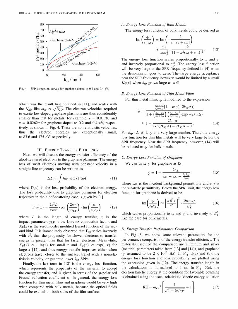
Fig. 3. SPP dispersion curves for 1-nm thick aluminum and silver films.
A 2-D thin film of vanishing thickness will have anincreased ksp. Hypothetically, if the metal films can be madeextremely thin (e.g., 1-nm thickness), we can take lim(� →0)in (1) and thus the dispersion relation becomes
ksp =√(
2εd
εm�
)2
+ εd
(ω
c
)2(5)
and
Re(ksp) ≈ 2ω2εd
ω2p[1 − x2ε∞]�. (6)
As ksp scales inversely with �, we can achieve very high kspfor low ω and v, as shown in Fig. 3.
We further examine the case for graphene, where theplasmon dispersion is given in terms of the 2-D conductivity
ksp = ω
c
√εd −
(2εdε0c
σ
)2
. (7)
The optical conductivity, σ is obtained from both the semi-classical model and random phase approximation, given by
σ(ω) = ie2 EF
π�2(ω + iγ )+ ie2
4π�ln
(2|EF | − (ω + iγ )�
2|EF | + (ω + iγ )�
)(8)
where the first term on the right represents the intrabandconductivity and the second term represents the interbandconductivity [8]. The constant e is the electronic charge and� is the reduced Planck’s constant
EF = �vF
√π N2D = �vF
√π
εdε0
eF (9)
is the Fermi level controllable by electric field F [9], andvF = 106 m/s is the Fermi velocity of graphene [10]. Thegraphene conductivity model is valid when EF � kB T ,where kB is the Boltzmann constant and T is the temperature.It is evident that ksp ∝ 1/
√N2D and we can thus see a
very strongly deflected plasmon dispersion curve toward thelow-frequency midinfrared regime, as observed from the plotin Fig. 4. Furthermore, we can establish the SPR frequencyof graphene when the real part as well as the imaginary partof the conductivity approaches zero, σ ′(ω) ≈ σ ′′(ω) ≈ 0, inwhich we get
ωsp = 5EF
3�(10)
OOI et al.: EFFICIENCIES OF ALOOF-SCATTERED ELECTRON BEAM 953
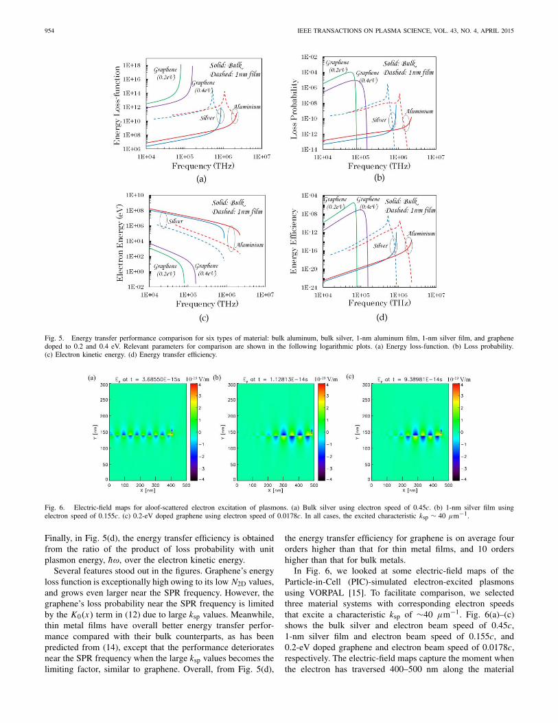
Fig. 4. SPP dispersion curves for graphene doped to 0.2 and 0.4 eV.
which was the result first obtained in [11], and scales withthe N2D like ωsp ∝ √
N2D. The electron velocities requiredto excite low-doped graphene plasmons are thus considerablysmaller than that for metals, for example, v = 0.0178c andv = 0.0262c for graphene doped to 0.2 and 0.4 eV, respec-tively, as shown in Fig. 4. These are nonrelativistic velocities,thus the electron energies are exceptionally small,at 83.6 and 175 eV, respectively.
III. ENERGY TRANSFER EFFICIENCY
Next, we will discuss the energy transfer efficiency of thealoof-scattered electrons to the graphene plasmons. The energyloss of swift electrons moving with constant velocity in astraight line trajectory can be written as
�E =∫
�ω · dω · �(ω) (11)
where �(ω) is the loss probability of the electron energy.The loss probability due to graphene plasmons for electrontrajectory in the aloof-scattering case is given by [1]
�SP(ω) = 2e2L
π�v2 · K0
(2ωz
vγLF
)· Im
(rp
ε0εd
)(12)
where L is the length of energy transfer, z is theimpact parameter, γLF is the Lorentz contraction factor, andK0(x) is the zeroth-order modified Bessel function of the sec-ond kind. It is immediately observed that �sp scales inverselywith v2, thus the propensity for slower electrons to transferenergy is greater than that for faster electrons. Meanwhile,K0(x) ∝ −ln(x) for small x and K0(x) ∝ exp(−x) forlarge x [12], and thus energy transfer improves either whenelectrons travel closer to the surface, travel with a nonrela-tivistic velocity, or generate lower ksp SPPs.
Finally, the last term in (12) is the energy loss function,which represents the propensity of the material to acceptthe energy transfer, and is given in terms of the p-polarizedFresnel reflection coefficient rp . In general, the energy lossfunction for thin metal films and graphene would be very highwhen compared with bulk metals, because the optical fieldscould be excited on both sides of the film surface.
A. Energy Loss Function of Bulk Metals
The energy loss function of bulk metals could be derived as
Im
(rp
ε0εd
)= Im
(− 2
ε0[εd + εm])
≈ ωγ
ε0ω2p
· 2
[1 − x2(εd + ε∞)]2 . (13)
The energy loss function scales proportionally to ω and γand inversely proportional to ω2
p . The energy loss functionwill be very large at the SPR frequency defined in (4) whenthe denominator goes to zero. The large energy acceptancenear the SPR frequency, however, would be limited by a smallK0(x) when ksp grows large as well.
B. Energy Loss Function of Thin Metal Films
For thin metal films, rp is modified to the expression
rp =εm−εdεd+εm
[1 − exp(−2ksp�)]1 +
(εm−εdεd+εm
) (εd−εmεd+εm
)exp(−2ksp�)
≈ 1 + 2ksp�
exp(2ksp�) − 2ksp� − 1. (14)
For ksp · � 1, rp is a very large number. Thus, the energyloss function for thin film metals will be very large below theSPR frequency. Near the SPR frequency, however, (14) willbe reduced to rp for bulk metals.
C. Energy Loss Function of Graphene
We can write rp for graphene as [5]
rp = 1 − 2εd1
εd1 + εd2 + iσkspε0ω
(15)
where εd1 is the incident background permittivity and εd2 isthe substrate permittivity. Below the SPR limit, the energy lossfunction for graphene is derived to be
Im
(rp
ε0εd
)≈
[π�
2c
e2
]2
· 16ε0ωγ
E2F
(16)
which scales proportionally to ω and γ and inversely to E2F
like the case for bulk metals.
D. Energy Transfer Performance Comparison
In Fig. 5, we show some relevant parameters for theperformance comparison of the energy transfer efficiency. Thematerials used for the comparison are aluminum and silver(material parameters taken from [13] and [14]), and graphene(γ assumed to be 2 × 10¹² Hz). In Fig. 5(a) and (b), theenergy loss function and loss probability are plotted usingthe expression given in (12). The energy transfer length inthe calculations is normalized to 1 m. In Fig. 5(c), theelectron kinetic energy at the condition for favorable couplingis obtained using the usual relativistic kinetic energy equation
KE = mec2
[1√
1 − (v/c)2− 1
]. (17)
954 IEEE TRANSACTIONS ON PLASMA SCIENCE, VOL. 43, NO. 4, APRIL 2015
Fig. 5. Energy transfer performance comparison for six types of material: bulk aluminum, bulk silver, 1-nm aluminum film, 1-nm silver film, and graphenedoped to 0.2 and 0.4 eV. Relevant parameters for comparison are shown in the following logarithmic plots. (a) Energy loss-function. (b) Loss probability.(c) Electron kinetic energy. (d) Energy transfer efficiency.
Fig. 6. Electric-field maps for aloof-scattered electron excitation of plasmons. (a) Bulk silver using electron speed of 0.45c. (b) 1-nm silver film usingelectron speed of 0.155c. (c) 0.2-eV doped graphene using electron speed of 0.0178c. In all cases, the excited characteristic ksp ∼ 40 μm−1.
Finally, in Fig. 5(d), the energy transfer efficiency is obtainedfrom the ratio of the product of loss probability with unitplasmon energy, hω, over the electron kinetic energy.
Several features stood out in the figures. Graphene’s energyloss function is exceptionally high owing to its low N2D values,and grows even larger near the SPR frequency. However, thegraphene’s loss probability near the SPR frequency is limitedby the K0(x) term in (12) due to large ksp values. Meanwhile,thin metal films have overall better energy transfer perfor-mance compared with their bulk counterparts, as has beenpredicted from (14), except that the performance deterioratesnear the SPR frequency when the large ksp values becomes thelimiting factor, similar to graphene. Overall, from Fig. 5(d),
the energy transfer efficiency for graphene is on average fourorders higher than that for thin metal films, and 10 ordershigher than that for bulk metals.
In Fig. 6, we looked at some electric-field maps of theParticle-in-Cell (PIC)-simulated electron-excited plasmonsusing VORPAL [15]. To facilitate comparison, we selectedthree material systems with corresponding electron speedsthat excite a characteristic ksp of ∼40 μm−1. Fig. 6(a)–(c)shows the bulk silver and electron beam speed of 0.45c,1-nm silver film and electron beam speed of 0.155c, and0.2-eV doped graphene and electron beam speed of 0.0178c,respectively. The electric-field maps capture the moment whenthe electron has traversed 400–500 nm along the material

OOI et al.: EFFICIENCIES OF ALOOF-SCATTERED ELECTRON BEAM 955
Fig. 7. Cherenkov radiation is possible in the shaded cone bounded by thelight line in vacuum and in a medium having refractive index of n = 3.An electron beam of 100-keV kinetic energy could excite graphene plasmonsin the terahertz spectrum.
surface. It is observed that even with the vastly varied electronbeam speeds (and hence the electron kinetic energies), theexcited plasmon electric fields are on the same order ofmagnitude, which clearly corroborates with the high excitationenergy efficiency of graphene plasmons compared with that ofsilver plasmons.
IV. POTENTIAL APPLICATIONS OF ALOOF-SCATTERED
GRAPHENE PLASMONS
Graphene’s high-energy transfer efficiency could be usedfor applications in generating coherent radiation. For example,one of the possible applications is the plasmon-controlledCherenkov radiation as mentioned previously. Liu et al. [4]have shown that the radiation spectrum of Cherenkov radia-tion, which is usually broadband, could be made frequencyselective by first exciting the metal plasmon modes, and theradiation frequency can be tuned over a narrow spectral rangein the visible and UV regime by tuning the electron beamvelocity. We took the configuration of [4] and replaced themetal layer with graphene. Fig. 7 shows that for a 100-keVelectron beam, we could potentially excite Cherenkovradiation modes in the 1–2-THz frequency spectrum. Thus,graphene could potentially be used for efficient terahertzradiation sources. Moreover, the graphene Cherenkov radiationspectrum has increased tunability: we can tune both theelectron beam velocity and also the Fermi level of graphenethrough an electrostatic gating. In cases where low-energyelectron beams are preferred and Cherenkov-type of radiationis not possible, it is still possible to induce coherent radiationfrom gratings [16]. Liu et al. [16] have recently shown that thecoherent radiation generated from graphene-on-gratings are400 times stronger than the conventional dielectric materials.
REFERENCES
[1] F. J. García de Abajo, “Optical excitations in electron microscopy,”Rev. Modern Phys., vol. 82, no. 1, pp. 209–275, Jan. 2010.
[2] R. H. Ritchie, “Plasma losses by fast electrons in thin films,” Phys. Rev.,vol. 106, no. 5, pp. 874–881, Jun. 1957.
[3] J. Lecante, Y. Ballu, and D. M. Newns, “Electron-surface-plasmonscattering using a parabolic nontouching trajectory,” Phys. Rev. Lett.,vol. 38, no. 1, pp. 36–40, Jan. 1977.
[4] S. Liu et al., “Surface polariton Cherenkov light radiation source,”Phys. Rev. Lett., vol. 109, no. 15, p. 153902, Oct. 2012.
[5] F. J. García de Abajo, “Multiple excitation of confined grapheneplasmons by single free electrons,” ACS Nano, vol. 7, no. 12,pp. 11409–11419, Nov. 2013.
[6] A. Alù and N. Engheta, “Optical nanotransmission lines: Synthesis ofplanar left-handed metamaterials in the infrared and visible regimes,”J. Opt. Soc. Amer. B, vol. 23, no. 3, pp. 571–583, Mar. 2006.
[7] L. Ju et al., “Graphene plasmonics for tunable terahertz metamaterials,”Nature Nanotechnol., vol. 6, no. 10, pp. 630–634, Sep. 2011.
[8] M. Jablan, H. Buljan, and M. Soljacic, “Plasmonics in grapheneat infrared frequencies,” Phys. Rev. B, vol. 80, no. 24, p. 245435,Dec. 2009.
[9] K. S. Novoselov et al., “Electric field effect in atomically thin carbonfilms,” Science, vol. 306, no. 5696, pp. 666–669, Oct. 2004.
[10] K. S. Novoselov et al., “Two-dimensional gas of massless Dirac fermionsin graphene,” Nature, vol. 438, no. 7065, pp. 197–200, Nov. 2005.
[11] S. A. Mikhailov and K. Ziegler, “New electromagnetic mode ingraphene,” Phys. Rev. Lett., vol. 99, no. 1, p. 016803, Jul. 2007.
[12] M. Abramowitz and I. A. Stegun, Handbook of Mathematical Functions.New York, NY, USA: Dover, 1965.
[13] E. D. Palik, Handbook of Optical Constants of Solids. Amsterdam,The Netherlands: Elsevier, 1997.
[14] P. B. Johnson and R. W. Christy, “Optical constants of the noble metals,”Phys. Rev. B, vol. 6, no. 12, pp. 4370–4379, Dec. 1972.
[15] Tech-X Corporation. [Online]. Available: http://www.txcorp.com,accessed Dec. 1, 2014.
[16] S. Liu et al., “Coherent and tunable terahertz radiation from graphenesurface plasmon polaritons excited by an electron beam,” Appl. Phys.Lett., vol. 104, no. 20, p. 201104, May 2014.
Kelvin J. A. Ooi (GSM’11–M’15) received theB.Eng. (Hons.) and Ph.D. degrees in electricaland electronic engineering from Nanyang Techno-logical University, Singapore, in 2010 and 2014,respectively, with a major in photonics.
He joined the Singapore University of Technologyand Design, Singapore, as a Research Assistant,in 2013, where he is currently a Post-DoctoralResearch Fellow under the joint supervisionof Prof. L. K. Ang and Prof. D. T. H. Tan.His current research interests include nanophotonics,
electrically excited plasmonics, graphene plasmonics, and nonlinear optics.
Wee Shing Koh (S’03–M’07–SM’14) was born inSingapore in 1977. He received the B.Eng. (Hons.)and Ph.D. degrees in electrical and electronics engi-neering from Nanyang Technological University,Singapore, in 2002 and 2007, respectively.
He has been with the Institute of High Perfor-mance Computing (IHPC), Agency for Science,Technology and Research, Singapore, as a ResearchEngineer, since 2006. He is currently the CapabilityGroup Manager and a Scientist with the Departmentof Electronics and Photonics, IHPC. He has authored
over 50 journal and conference papers. His current research interests includeorganic solar cell devices, computational plasmonics for thin-film solarcells, sensors and microelectronics, field emission theory, multidimensionalspace-charge-limited transport, and particle-in-cell simulations for plasma,nanophotonic, and nanoelectronic applications.
Dr. Koh was a recipient of the inaugural IHPC Independent InvestigatorshipAward from 2011 to 2013. He is the Chairman of the IEEE Nuclear andPlasma Sciences Society Chapter in Singapore.
956 IEEE TRANSACTIONS ON PLASMA SCIENCE, VOL. 43, NO. 4, APRIL 2015
Hong Son Chu received the B.E. degree inelectronics and telecommunications engineeringfrom the Ho Chi Minh City University of Tech-nology, Ho Chi Minh City, Vietnam, in 1999, andthe M.S. degree in propagation, telecommunications,and remote sensing and the Ph.D. degree in electron-ics from the University of Nice Sophia Antipolis,Nice, France, in 2000 and 2004, respectively.
He joined the Computational Electromagnet-ics Research Laboratory, University of Victoria,Victoria, BC, Canada, from 2004 to 2005, as the
Natural Sciences and Engineering Research Council Post-Doctoral Fellow.Since 2006, he has been with the Institute of High Performance Computing,Agency for Science, Technology and Research, Singapore, as a Scientist andthe Capability Group Manager of the Photonics and Plasmonics Group underthe Department of Electronics and Photonics. He has authored or co-authoredover 50 technical papers in international referred journals and conferences.His current research interests include plasmonic and photonic nanostructuresfrom fundamentals to devices and applications, and computational techniquesfor electromagnetics from microwave to optical wavelengths.
Dawn T. H. Tan received the B.A.Sc. degree from the University of BritishColumbia, Vancouver, BC, USA, and the M.S. and Ph.D. degrees from theUniversity of California at San Diego, La Jolla, CA, USA.
She was a Visiting Scholar with the Massachusetts Institute of Technology,Cambridge, MA, USA, from 2013 to 2014. She was a Senior Engineer withLuxtera Inc., Carlsbad, CA, USA, and then a Leader in CMOS Photonics,where she was involved in silicon photonics. She is currently an AssistantProfessor with the Singapore University of Technology and Design, Singapore.She has authored three book chapters and over 40 refereed journal andconference articles in the field of integrated optics, silicon photonics, andnonlinear optics.
Prof. Tan was the recipient of the Best Paper Award at the Workshop onInformation Optics in 2009.
Lay Kee Ang (GSM’95–M’00–SM’08) receivedthe B.S. degree from the Department of NuclearEngineering, National Tsing Hua University,Hsinchu, Taiwan, in 1994, and the M.S. and Ph.D.degrees from the Department of Nuclear Engineeringand Radiological Sciences, University of Michigan,Ann Arbor, MI, USA, in 1996 and 1999,respectively.
He received a fellowship to work as theLos Alamos National Laboratory Director anda Post-Doctoral Fellow with the Plasma Physics
Applications Group, Applied Physics Division, Los Alamos, NM, USA,from 1999 to 2001. He was an Assistant Professor and a Tenured AssociateProfessor with the Division of Microelectronics, School of Electrical andElectronic Engineering, Nanyang Technological University, Singapore, from2001 to 2011. He has been with the Singapore University of Technology andDesign, Singapore, since 2011, and is currently the Ph.D. Program Directorand a Faculty Member of the Engineering Product Development pillar.He has authored over 70 journal papers on these topics. His current researchinterests include electron emission from novel materials, ultrafast laserinduced photocathode, space charge limited current, multipactor discharge,plasmonics, and charge injection into solids.
Prof. Ang received several Window of Science Awards fromAFOSR-AOARD to be a short-term Visiting Scientist to USA. Hewas the Founding Chairman of the IEEE Nuclear and Plasma SciencesSociety Chapter in Singapore in 2012.


