Embed Size (px)
Citation preview
B.Tech project Report
ECG Telemonitoring System
Submitted in partial fulfilment of requirementsfor the award of the Degree of
Bachelor of TechnologyElectronics and Communication Engineering
FROM:
Engr Rana Muhammad Shakeel
https://www.facebook.com/EngnrShakeel
plz like my page:
https://www.facebook.com/Electrical4Electronics
For MORE PROJECTS:http://electro-technolgy.blogspot.com
DEPARTMENT OF ELECTRONICS & COMMUNICATION ENGINEERING
YOUNUS COLLEGE OF ENGINEERING & TECHNOLOGY,KOLLAM
ACKNOWLEDGEMENT
On submission of this project report on ‘Ecg
Telemonitoring System’, I am greatly indebted to all those
who helped me to make this project successful. First of all, I
would like to thank the Lord Almighty who helped me finish
this project on time.
I express my sincere thanks to Dr. S K Masud Hossain, the
Principal, Younus College of Engineering & Technology, for
providing opportunity and the environment to do this project
in our college.
I sincerely thank Mr. Rajeev S K, Head of the Department,
Electronics and Communication Engineering, for his encouragement
and constant support in making this project successful.
An excellent group of teaching and non-teaching staff had
helped me with this seminar. I owe much, to the assistance
they gave me while doing this project.
I would like to thank Mrs. Nisha A.V, Lecturer, Electronics
and Communication Engineering Department, for giving me
technical advice and timely instruction, without which I could
never have been able to complete the work in time.

I also wish to thank Mr.Baby John, Lecturer, Electronics and
Communication Engineering Department, for providing valuable
guidance.
Last, but not the least I would like to thank my parents
and friends for all the moral support and help that they have
given me.
Project Team
R
ABSRACT
The ECG telemonitoring system are composed of the portable
ECG terminal and the health monitoring center.The portable
ECG monitoring terminal connects to wireless network by the
zigbee wireless communication module. ECG signals are
sampled and processed by portable monitoring terminal and
the data acquired are sent to monitoring center server by
the zigbee link .The doctors judge the patient health state
by their experiment and the analyzed results of the ECG
analysis software

CONTENTS
• Objective
• Existing system
• Proposed system

• Block diagram
• Advantages
• Applications
• Conclusion
• References
OBJECTIVE
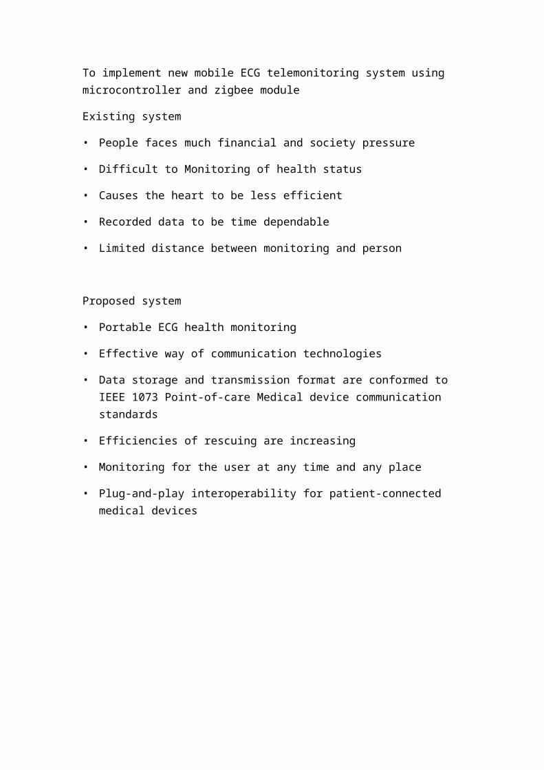
To implement new mobile ECG telemonitoring system using microcontroller and zigbee module
Existing system
• People faces much financial and society pressure
• Difficult to Monitoring of health status
• Causes the heart to be less efficient
• Recorded data to be time dependable
• Limited distance between monitoring and person
Proposed system
• Portable ECG health monitoring
• Effective way of communication technologies
• Data storage and transmission format are conformed to IEEE 1073 Point-of-care Medical device communication standards
• Efficiencies of rescuing are increasing
• Monitoring for the user at any time and any place
• Plug-and-play interoperability for patient-connected medical devices
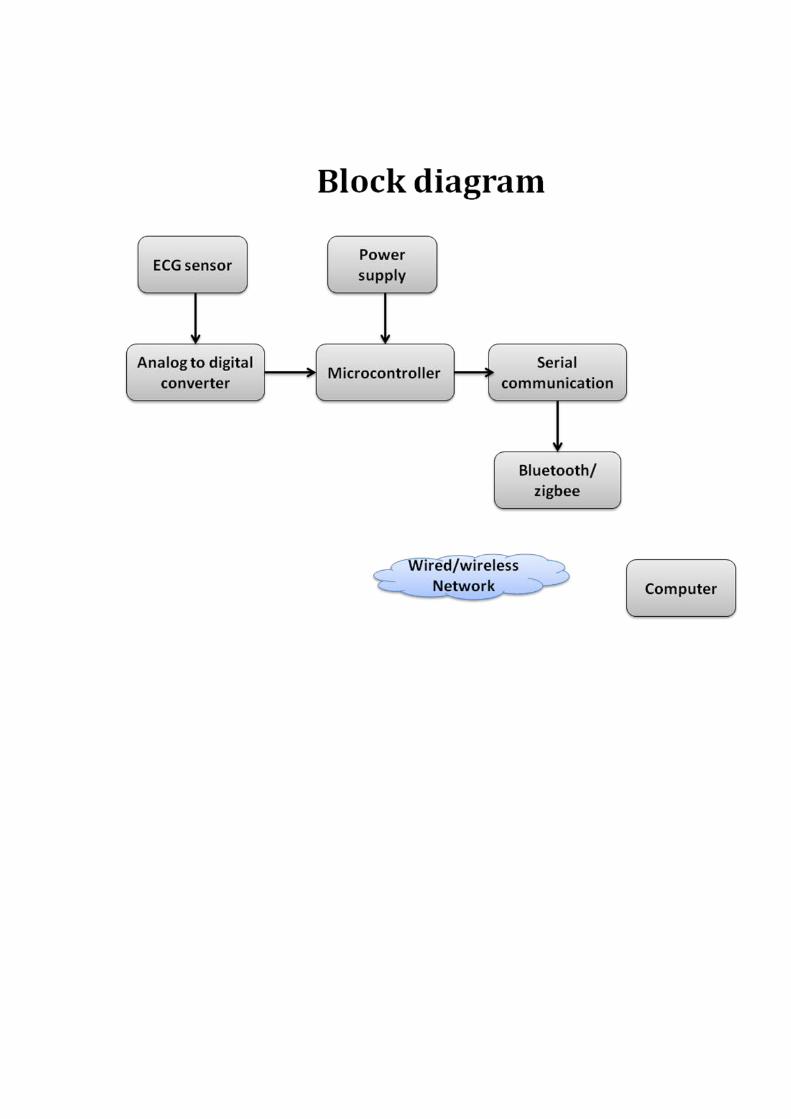
BLOCK DEFINITION
• The ECG telemonitoring system are composed of the portable ECG terminal and the health monitoring center
• The portable ECG monitoring terminal connects to wirelessnetwork by the zigbee wireless communication module
• ECG signals are sampled and processed by portable monitoring terminal and the data acquired are sent to monitoring center server by the zigbee link
• The doctors judge the patient health state by their experiment and the analyzed results of the ECG analysis software
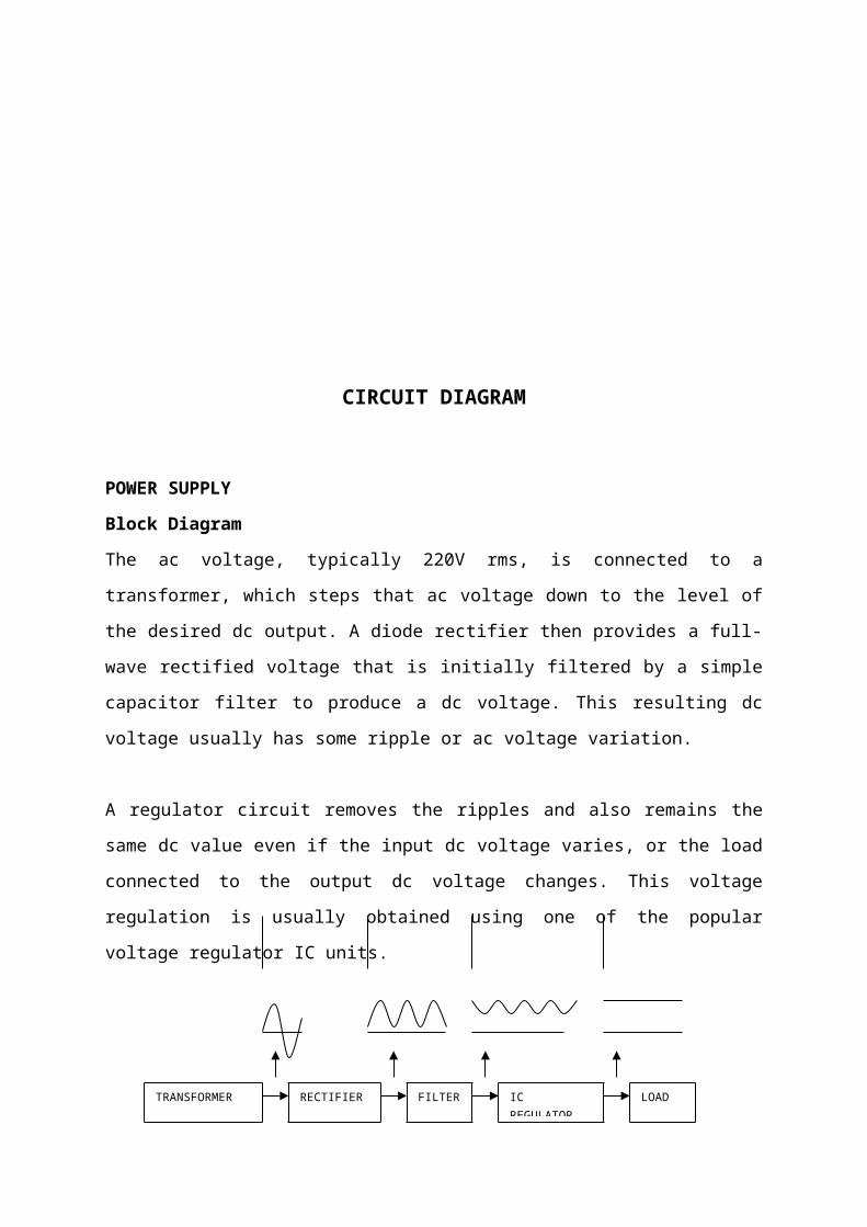
CIRCUIT DIAGRAM
POWER SUPPLY
Block Diagram
The ac voltage, typically 220V rms, is connected to a
transformer, which steps that ac voltage down to the level of
the desired dc output. A diode rectifier then provides a full-
wave rectified voltage that is initially filtered by a simple
capacitor filter to produce a dc voltage. This resulting dc
voltage usually has some ripple or ac voltage variation.
A regulator circuit removes the ripples and also remains the
same dc value even if the input dc voltage varies, or the load
connected to the output dc voltage changes. This voltage
regulation is usually obtained using one of the popular
voltage regulator IC units.
TRANSFORMER RECTIFIER FILTER IC REGULATOR
LOAD
Fig 5.3 Block Diagram of Power supply
Working principle
Transformer
The potential transformer will step down the power supply
voltage (0-230V) to (0-6V) level. Then the secondary of the
potential transformer will be connected to the precision
rectifier, which is constructed with the help of op–amp. The
advantages of using precision rectifier are it will give peak
voltage output as DC, rest of the circuits will give only RMS
output.
Bridge rectifier
When four diodes are connected as shown in figure, the circuit
is called as bridge rectifier. The input to the circuit is
applied to the diagonally opposite corners of the network, and
the output is taken from the remaining two corners.
Let us assume that the transformer is working properly and
there is a positive potential, at point A and a negative
potential at point B. the positive potential at point A will
forward bias D3 and reverse bias D4.
The negative potential at point B will forward bias D1 and
reverse D2. At this time D3 and D1 are forward biased and will
allow current flow to pass through them; D4 and D2 are reverse
biased and will block current flow.
The path for current flow is from point B through D1, up
through RL, through D3, through the secondary of the

transformer back to point B. this path is indicated by the
solid arrows. Waveforms (1) and (2) can be observed across D1
and D3.
One-half cycle later the polarity across the secondary of the
transformer reverse, forward biasing D2 and D4 and reverse
biasing D1 and D3. Current flow will now be from point A
through D4, up through RL, through D2, through the secondary
of T1, and back to point A. This path is indicated by the
broken arrows. Waveforms (3) and (4) can be observed across D2
and D4. The current flow through RL is always in the same
direction. In flowing through RL this current develops a
voltage corresponding to that shown waveform (5). Since
current flows through the load (RL) during both half cycles of
the applied voltage, this bridge rectifier is a full-wave
rectifier.
One advantage of a bridge rectifier over a conventional full-
wave rectifier is that with a given transformer the bridge
rectifier produces a voltage output that is nearly twice that
of the conventional full-wave circuit.
This may be shown by assigning values to some of the
components shown in views A and B. assume that the same
transformer is used in both circuits. The peak voltage
developed between points X and y is 1000 volts in both
circuits. In the conventional full-wave circuit shown—in view
A, the peak voltage from the center tap to either X or Y is
500 volts. Since only one diode can conduct at any instant,
the maximum voltage that can be rectified at any instant is
500 volts.
The maximum voltage that appears across the load resistor is
nearly-but never exceeds-500 v0lts, as result of the small
voltage drop across the diode. In the bridge rectifier shown
in view B, the maximum voltage that can be rectified is the
full secondary voltage, which is 1000 volts. Therefore, the
peak output voltage across the load resistor is nearly 1000
volts. With both circuits using the same transformer, the
bridge rectifier circuit produces a higher output voltage than
the conventional full-wave rectifier circuit.
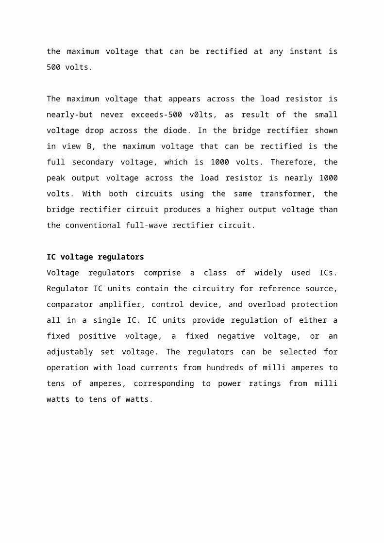
IC voltage regulators
Voltage regulators comprise a class of widely used ICs.
Regulator IC units contain the circuitry for reference source,
comparator amplifier, control device, and overload protection
all in a single IC. IC units provide regulation of either a
fixed positive voltage, a fixed negative voltage, or an
adjustably set voltage. The regulators can be selected for
operation with load currents from hundreds of milli amperes to
tens of amperes, corresponding to power ratings from milli
watts to tens of watts.
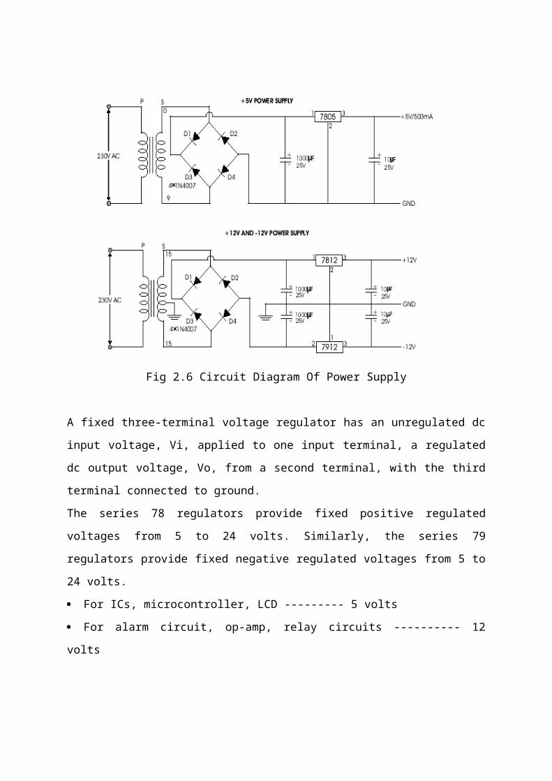
Fig 2.6 Circuit Diagram Of Power Supply
A fixed three-terminal voltage regulator has an unregulated dc
input voltage, Vi, applied to one input terminal, a regulated
dc output voltage, Vo, from a second terminal, with the third
terminal connected to ground.
The series 78 regulators provide fixed positive regulated
voltages from 5 to 24 volts. Similarly, the series 79
regulators provide fixed negative regulated voltages from 5 to
24 volts.
For ICs, microcontroller, LCD --------- 5 volts
For alarm circuit, op-amp, relay circuits ---------- 12
volts
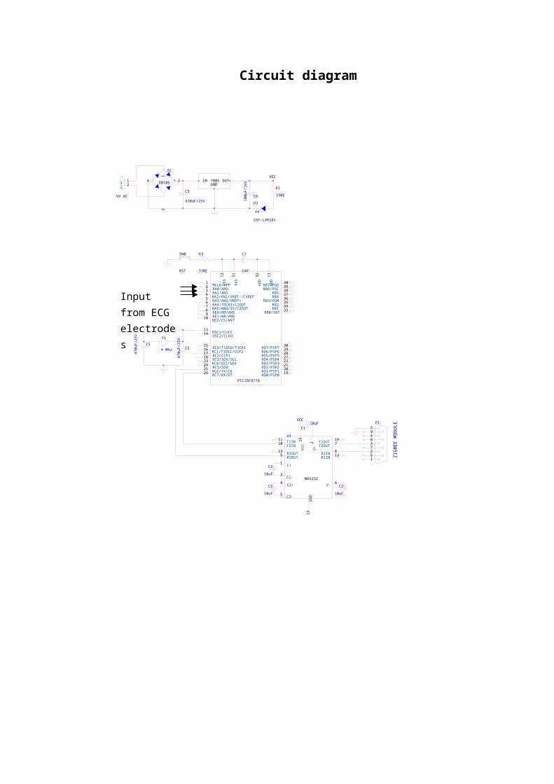
Circuit diagram
VCC
VCC
Input from ECG electrodes
9V AC
121
2
C6
100uF/16
V
R3330E
C5
470uF/25V
- +
D1
DB106
1
2
3
4
D3
SSF-LXH101
C310uF
Y1
4 Mhz
C7
CAP
PIC16F877A
12345678910
1112
1314
15161718
1920
4039383736353433
3231
30292827
26252423 22
21
MCLR/VPPRA0/ANORA1/AN1RA2/AN2/VREF-/CVREFRA3/AN3/VREF+RA4/TOCKI/C1OUTRA5/AN4/SS/C2OUTREO/RD/AN5RE1/WR/AN6RE2/CS/AN7
VDD
VSS
OSC1/CLKIOSC2/CLKO
RCO/T1OSO/T1CKIRC1/T1OSI/CCP2RC2/CCP1RC3/SCK/SCL
RD0/PSP0RD1/PSP1
RB7/PGDRB6/PGC
RB5RB4
RB3/PGMRB2RB1
RB0/INT
VDD
VSS
RD7/PSP7RD6/PSP6RD5/PSP5RD4/PSP4
RC7/RX/DTRC6/TX/CKRC5/SDORC4/SDI/SDA RD3/PSP3
RD2/PSP2
R3
330E
C5
470u
F/25V
C5
470uF/25
V
C110uF
SW0
RST
U1
MAX232
138
1110
1
3
4
5
2
6
129
14716
15
R1INR2IN
T1INT2IN
C+
C1-
C2+
C2-
V+
V-
R1OUTR2OUT
T1OUTT2OUT
VCC
GND
C310uF
P1
ZIGBEE MODULE
594837261
C310uF
7805GND
OUTIN
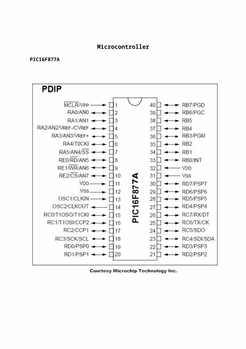
Microcontroller
PIC16F877A
Major Blocks in the PIC MCU
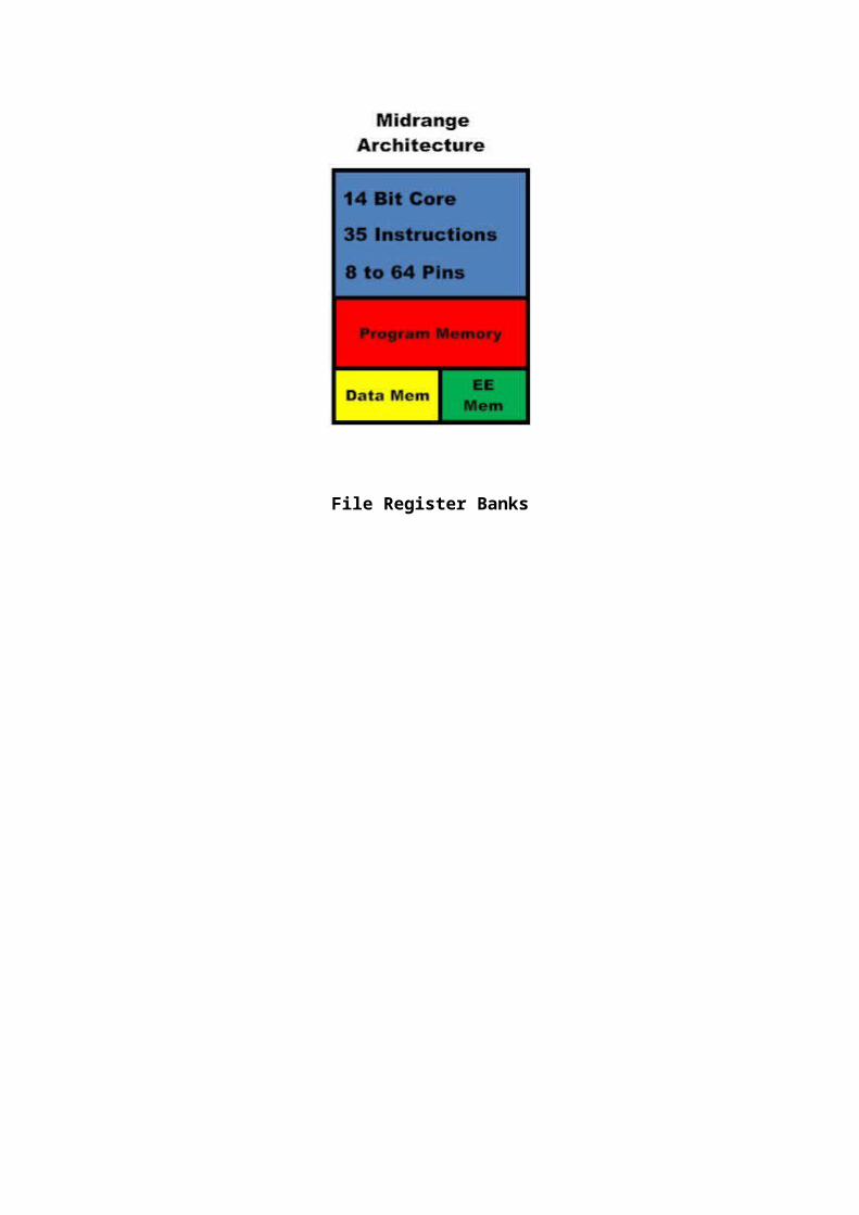
The major parts of the PIC MCU (Microcontroller Unit) that we will be concerned with are the program memory, data memory which is also called file registers, and the Working Register,and finally the EEPROM memory section.
Program Memory ----- 14 bit word length
File Register Memory (Data Memory) ----- 8 bit word length
EEPROM Memory ----- 8 bit word length ---- separate address space
Working Register ----- Byte wide used in most instructions
Program Memory
The program memory in the PIC16F877A has a total of 8K words. The word length for the midrange family of PIC microcontrollers is 14 bits long. Because each word uses 14 bits this amount of memory is roughly equivalent to 14K bytes.The program memory can be made up of EPROM using the 16CXXX parts or it can have FLASH memory as in the 16FXXX parts. After the program memory has been programmed it will retain the program even if power is lost. Therefore program memory issaid to be nonvolatile.
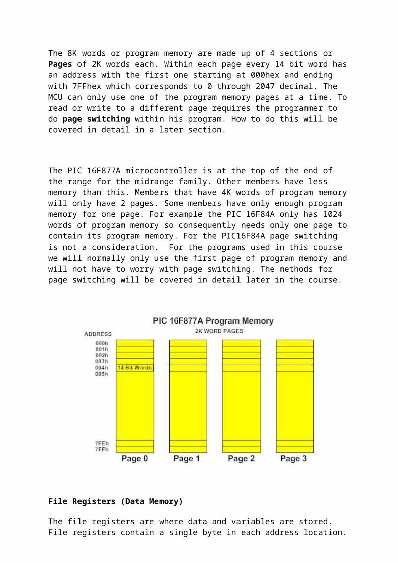
The 8K words or program memory are made up of 4 sections or Pages of 2K words each. Within each page every 14 bit word hasan address with the first one starting at 000hex and ending with 7FFhex which corresponds to 0 through 2047 decimal. The MCU can only use one of the program memory pages at a time. Toread or write to a different page requires the programmer to do page switching within his program. How to do this will be covered in detail in a later section.
The PIC 16F877A microcontroller is at the top of the end of the range for the midrange family. Other members have less memory than this. Members that have 4K words of program memorywill only have 2 pages. Some members have only enough program memory for one page. For example the PIC 16F84A only has 1024 words of program memory so consequently needs only one page tocontain its program memory. For the PIC16F84A page switching is not a consideration. For the programs used in this course we will normally only use the first page of program memory andwill not have to worry with page switching. The methods for page switching will be covered in detail later in the course.
File Registers (Data Memory)
The file registers are where data and variables are stored. File registers contain a single byte in each address location.
File registers will not retain their contents when power is lost and therefore is said to be volatile memory.
File Registers are considered the data memory section of the MCU. File registers can be broken down into two types of data storage. General purpose registers (GPR) are used by the programmer for normal calculations and temporary data storage.Special Function registers (SFR) are used to control various internal functions contained within the microcontroller such as interrupts, serial communications, timers and counters, A/Dconverters, program counter, port direction control and many others. Special Function registers will have a name associatedwith them such as TMR0, STATUS, PORTA, PORTB, etc. Each Special Function register allows control or access to data associated with a particular hardware function within the microcontroller. General purpose registers do not have a name since they can be used for any purpose the programmer designates. After a power-up any special function registers that are going to be used must be loaded with the necessary setup data before they can be used.
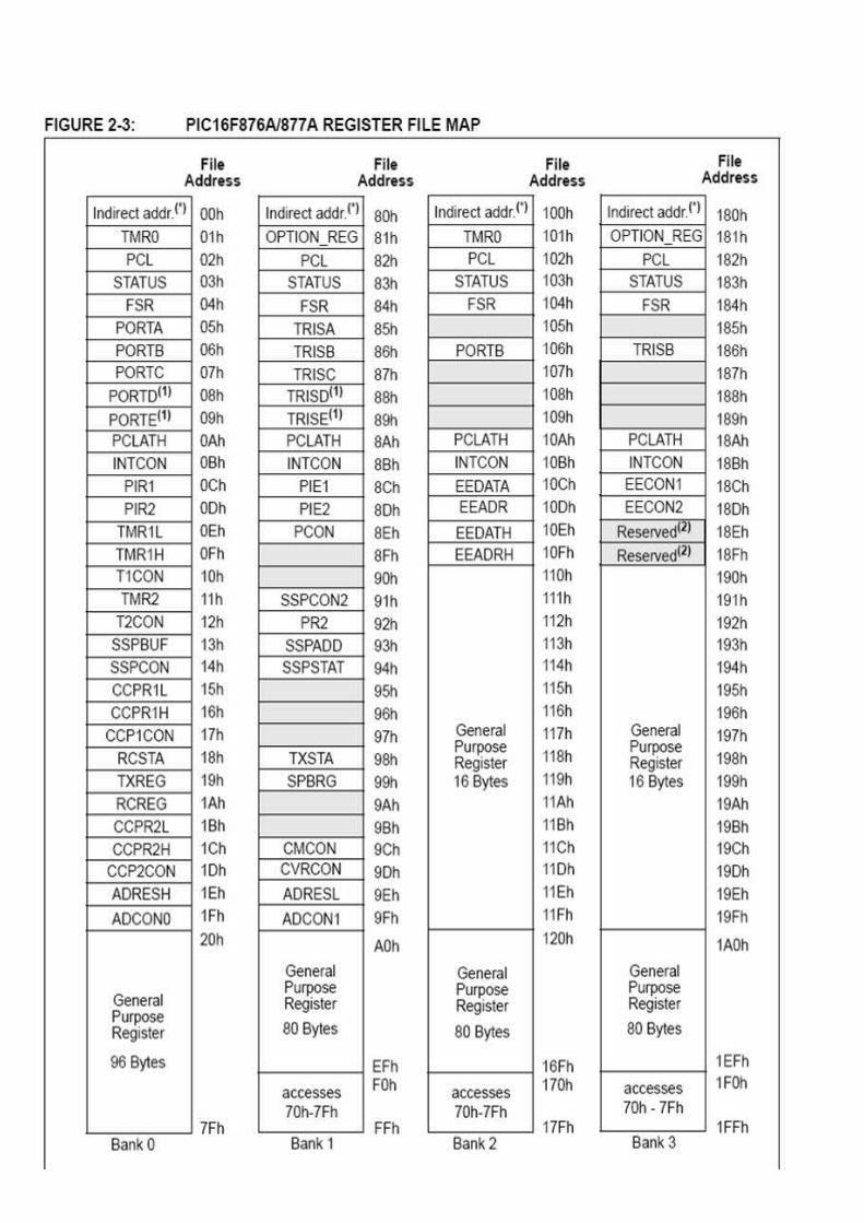
The file registers in data memory are divided up into Banks similar to the way program memory is divided into pages. Each Bank can hold up to 128 bytes and uses addresses from 00h to 7Fh. Notice in the image of the register file map that in eachbank the special function registers always start at address 00h and go up to a certain address at which point the general purpose registers begin. If all four banks contained 128 byteseach there would be 512 bytes total in the file register space. However not all locations are used. The byte locations tinted in grey are not available. Also in banks 1, 2 and 3 thelast 16 bytes all map to the same 16 bytes that are in bank 0.After these considerations we find that there are actually 368bytes of General Purpose Register Space.
Other microcontrollers that are at the lower end of the midrange product line may have only 2 banks that contain even fewer bytes than the 128 bytes in each bank of the PIC 16F877A. For example the PIC 16F84A has 2 banks with each bank
having addresses between 0 and 4Fh. This MCU has a total of 68bytes of general purpose file register space.
We will be using all 4 banks of the file register space available to the PIC 16F877A in our programs. The methods usedto switch banks will be covered in detail in a later programming section of the course.
EEPROM Memory
The last type of memory we will deal with is EEPROM. This memory is nonvolatile meaning that it will retain its data even if the power is lost. EEPROM is normally used to store parameter data that needs to be saved over a long period over many power-up and power-down cycles. Writing to EEPROM involves a more complex series of steps than writing to the File Registers. Each write cycles is very slow compared to writing to the File Registers. However reading is much simplerand much faster. The procedures for using this type of memory will be covered in an intermediate course.
The PIC16F877A has 256 bytes of EEPROM memory. The EEPROM memory is separate from program memory and data memory. It hasit own address space. To read or write to EEPROM memory the Special Function Registers are used such as EEDATA and EEADR.
File Register Banks
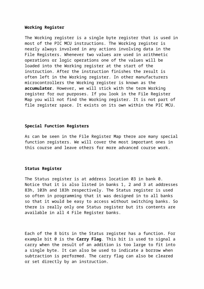
Working Register
The Working register is a single byte register that is used inmost of the PIC MCU instructions. The Working register is nearly always involved in any actions involving data in the File Registers. Whenever two values are used in arithmetic operations or logic operations one of the values will be loaded into the Working register at the start of the instruction. After the instruction finishes the result is often left in the Working register. In other manufacturers microcontrollers the Working register is known as the accumulator. However, we will stick with the term Working register for our purposes. If you look in the File Register Map you will not find the Working register. It is not part of file register space. It exists on its own within the PIC MCU.
Special Function Registers
As can be seen in the File Register Map there are many specialfunction registers. We will cover the most important ones in this course and leave others for more advanced course work.
Status Register
The Status register is at address location 03 in bank 0. Notice that it is also listed in banks 1, 2 and 3 at addresses83h, 103h and 183h respectively. The Status register is used so often in programming that it was designed in to all banks so that it would be easy to access without switching banks. Sothere is really only one Status register but its contents are available in all 4 File Register banks.
Each of the 8 bits in the Status register has a function. For example bit 0 is the Carry Flag. This bit is used to signal a carry when the result of an addition is too large to fit into a single byte. It can also be used to indicate a borrow when subtraction is performed. The carry flag can also be cleared or set directly by an instruction.
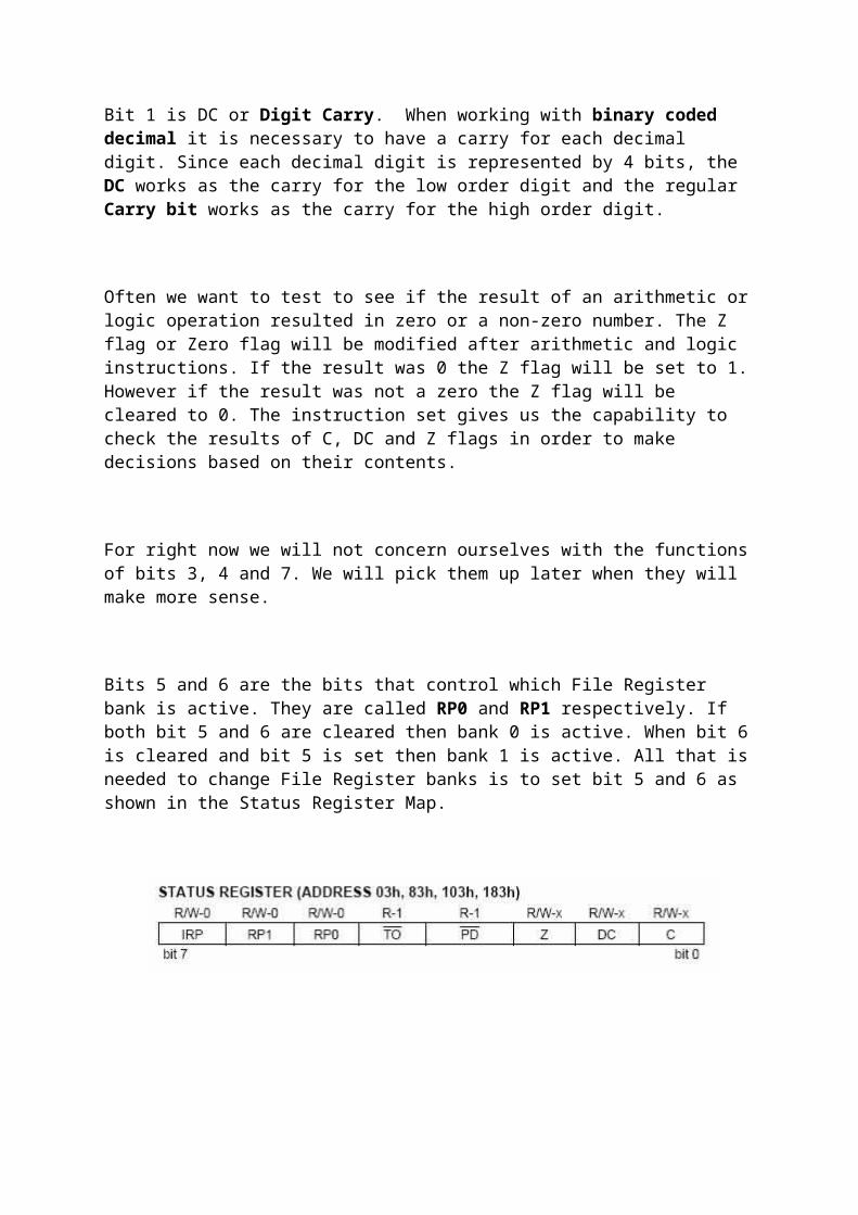
Bit 1 is DC or Digit Carry. When working with binary coded decimal it is necessary to have a carry for each decimal digit. Since each decimal digit is represented by 4 bits, the DC works as the carry for the low order digit and the regular Carry bit works as the carry for the high order digit.
Often we want to test to see if the result of an arithmetic orlogic operation resulted in zero or a non-zero number. The Z flag or Zero flag will be modified after arithmetic and logic instructions. If the result was 0 the Z flag will be set to 1.However if the result was not a zero the Z flag will be cleared to 0. The instruction set gives us the capability to check the results of C, DC and Z flags in order to make decisions based on their contents.
For right now we will not concern ourselves with the functionsof bits 3, 4 and 7. We will pick them up later when they will make more sense.
Bits 5 and 6 are the bits that control which File Register bank is active. They are called RP0 and RP1 respectively. If both bit 5 and 6 are cleared then bank 0 is active. When bit 6is cleared and bit 5 is set then bank 1 is active. All that isneeded to change File Register banks is to set bit 5 and 6 as shown in the Status Register Map.
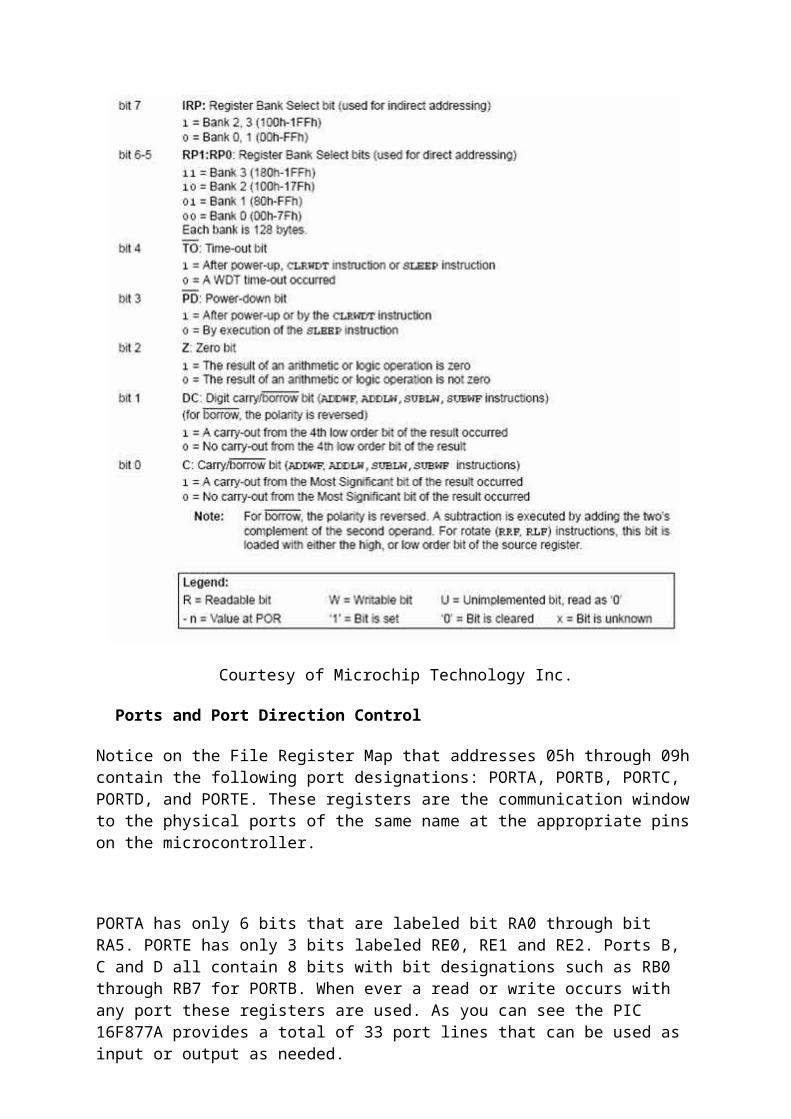
Courtesy of Microchip Technology Inc.
Ports and Port Direction Control
Notice on the File Register Map that addresses 05h through 09hcontain the following port designations: PORTA, PORTB, PORTC, PORTD, and PORTE. These registers are the communication windowto the physical ports of the same name at the appropriate pinson the microcontroller.
PORTA has only 6 bits that are labeled bit RA0 through bit RA5. PORTE has only 3 bits labeled RE0, RE1 and RE2. Ports B, C and D all contain 8 bits with bit designations such as RB0 through RB7 for PORTB. When ever a read or write occurs with any port these registers are used. As you can see the PIC 16F877A provides a total of 33 port lines that can be used as input or output as needed.
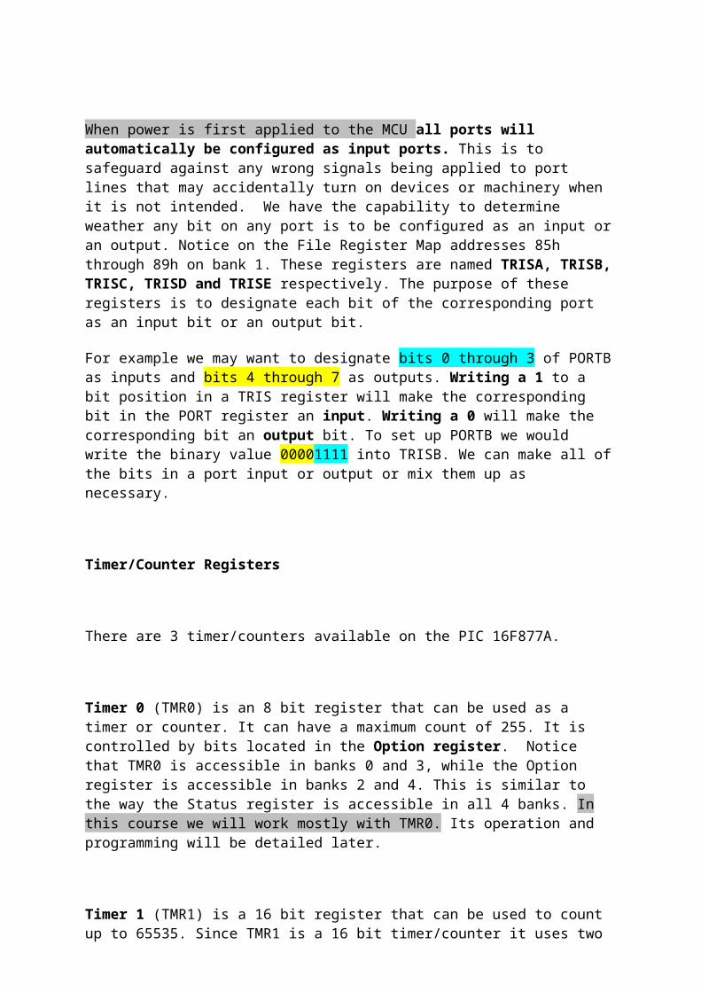
When power is first applied to the MCU all ports will automatically be configured as input ports. This is to safeguard against any wrong signals being applied to port lines that may accidentally turn on devices or machinery when it is not intended. We have the capability to determine weather any bit on any port is to be configured as an input oran output. Notice on the File Register Map addresses 85h through 89h on bank 1. These registers are named TRISA, TRISB,TRISC, TRISD and TRISE respectively. The purpose of these registers is to designate each bit of the corresponding port as an input bit or an output bit.
For example we may want to designate bits 0 through 3 of PORTBas inputs and bits 4 through 7 as outputs. Writing a 1 to a bit position in a TRIS register will make the corresponding bit in the PORT register an input. Writing a 0 will make the corresponding bit an output bit. To set up PORTB we would write the binary value 00001111 into TRISB. We can make all ofthe bits in a port input or output or mix them up as necessary.
Timer/Counter Registers
There are 3 timer/counters available on the PIC 16F877A.
Timer 0 (TMR0) is an 8 bit register that can be used as a timer or counter. It can have a maximum count of 255. It is controlled by bits located in the Option register. Notice that TMR0 is accessible in banks 0 and 3, while the Option register is accessible in banks 2 and 4. This is similar to the way the Status register is accessible in all 4 banks. In this course we will work mostly with TMR0. Its operation and programming will be detailed later.
Timer 1 (TMR1) is a 16 bit register that can be used to count up to 65535. Since TMR1 is a 16 bit timer/counter it uses two
bytes TMR1L addressed at 0Eh and TMR1H at 0Fh in bank 0 as one16 bit register. TMR1CON at address 10h has the control and status bits associated with Timer 1.
Timer 2 (TMR2) is another 8 bit timer counter with some special features that make it useful for various control operations. TMR2 and TMR2CON are located at 11h and 12h in bank 0 respectively.
Other Special Function Registers
Other SFR registers such as those involved with interrupts, Analog-to-Digital conversion will be covered when we discuss the programming of those functions. We will also cover registers used in indirect addressing such as the FSR. As you can see from looking at the Register File Map there is a wealth of registers and functionality available to the PIC 16F877A. An extensive coverage for much of this capability will have to be relegated to a course that goes beyond the basics.
PIC 16F877A Pinout
The midrange family of microcontrollers offer a wealth of features and functions. All functions are not available at onetime due to the limited number of pins. A typical 40 pin dual inline package for the PIC 16F877A is shown below. Notice thateach pin has mulitple functions. For example pin 5 can be usedas an input/output port pin RA2, an analog input channel AN3,or a positive voltage reference.
ADVANTAGES
Low cost and high coverage
Secure transmission solution
Efficient exchange of vital signs
Easy to interfacing medical instrument to computer

Applications
Monitoring and control platforms
Electronic medical record systems
Bio-medical applications
Database management systems

PCB FABRICATION
Printed circuit boards can be fabricated by:
Using paints and acid resist inks
Screen printing method
Photographic method
First the copper clad sheet is cut according to the size. Then
it is mechanically and chemically cleaned using thinner.
USING PAINTS AND ACID RESIST INKS
The required printed circuit layout is drawn on the
cleaned PCB using paint. Wax coated eyebrow pencil and stencil
correction fluid can be used. Commercially available “DALO”
pen in which the acid resist ink is used can also be used for
drawing the layout. After drying, it is etched in Ferric
Chloride solution having specific gravity of 1.4.With this
solution, complete etching with the exposed copper area will
be over in around 20 minutes.
SCREEN PRINTING METHOD
This method is commonly used for mass production of PCBs.
a. Screen preparation
An epical monofilament nylon cloth named as belting cloth
is used. For printed circuit boards, fine mesh cloth is
used. Commercially available 300
mesh cloth is suitable. The screen cloth is uniformly
stretched over a wooden frame and stapled. The screen is
then cleaned.
b. Layout preparation
The required PCB layout is drawn on a tracing sheet using
Indian ink for the actual size as it can be used as
positive. Using lith film positive can be obtained
through photographic process.The lith film is chosen for
contrast. Drawing thin lines using Indian film is
difficult. So using commercially available stickers , the
PCB layout is drawn for *2 of *4 size.It is then reduced
to actual size by process camera.

TRANSFER OF PCB LAYOUT ON THE SCREEN
Direct Method
Preparation of light sensitive solution
After preparing the emulsion, take care that they are not
exposed to bright light. It should be noted that even if
properly stored, the solution would last only 3 to 4 days as a
photographic emulsion. To dissolve PVA in water, first soak
powder in water for about half an hour. Then heat the solution
in a water bath with constant stirring till you get a uniform
solution. Allow to cool down and then keep it in a bottle as a
stock solution. This solution without other ingredients can be
kept for a very long time. Same procedure is to be used for
dissolving gelatin but it should be noted that the solution on
cooling will solidify into a jelly form.
The emulsion thus prepared should be uniformly and evenly
coated on the screen. The solution should be evened out from
inside to obtain a smooth
even coating. The screen after coating should be allowed to
dry in total darkness.
When the screen is dry , expose it by putting it in firm
contact with the positive, giving about ½ minute of rich
sunlight or about 2 minutes of artificial light. After
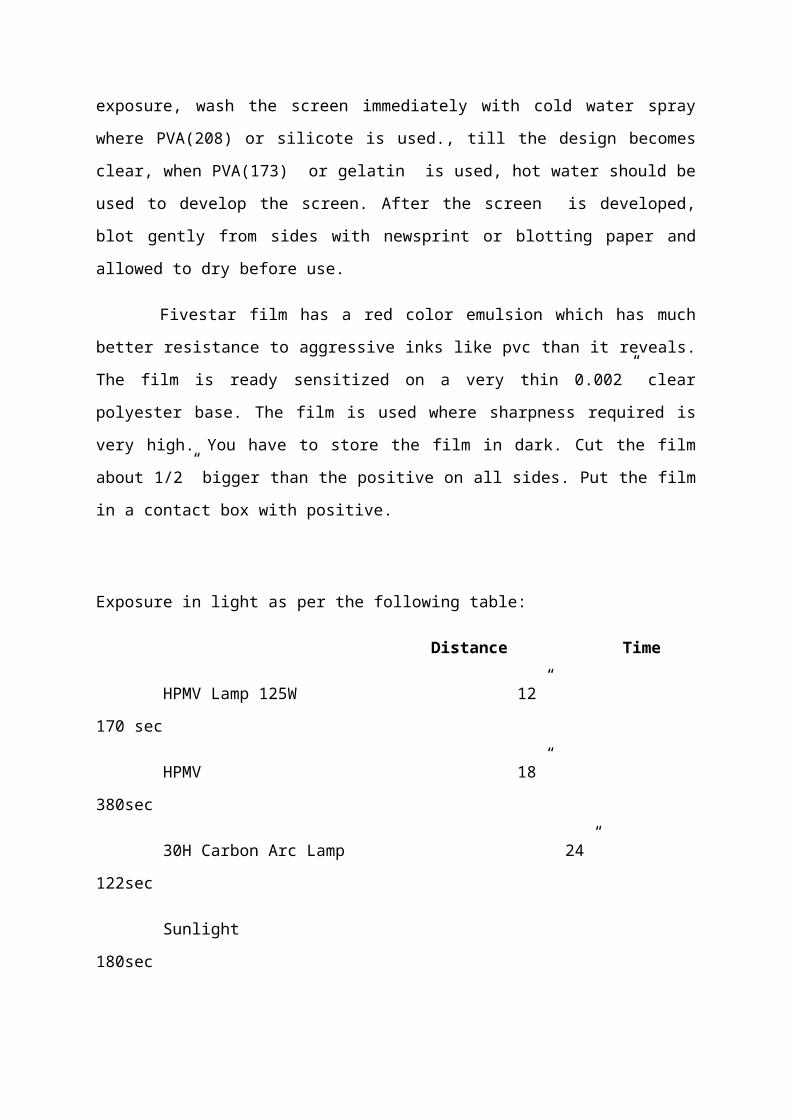
exposure, wash the screen immediately with cold water spray
where PVA(208) or silicote is used., till the design becomes
clear, when PVA(173) or gelatin is used, hot water should be
used to develop the screen. After the screen is developed,
blot gently from sides with newsprint or blotting paper and
allowed to dry before use.
Fivestar film has a red color emulsion which has much
better resistance to aggressive inks like pvc than it reveals.
The film is ready sensitized on a very thin 0.002” clear
polyester base. The film is used where sharpness required is
very high. You have to store the film in dark. Cut the film
about 1/2” bigger than the positive on all sides. Put the film
in a contact box with positive.
Exposure in light as per the following table:
Distance Time
HPMV Lamp 125W 12”
170 sec
HPMV 18”
380sec
30H Carbon Arc Lamp 24”
122sec
Sunlight
180sec

For developing prepare a solution of hydrogen peroxide.
Place the film in a tray with emulsion side up or put over the
solution gently taking care that the entire film is covered
with the solution.
Rock the tray gently, keep the film thus developed in the
developer for 1 min, take the film out of hydrogen peroxide
and place it in warm water. Rock continuously till the design
is clear. Gently spray water to help cleaning of the design
much faster. When the film is thoroughly washed, wash under
cold water, spray or chill the film.
Keep the film with the emulsion side up which now feels
sticky. Place the cleaned screen in position so the wet film
sticks to it correctly with no air bubbles on the outside.
Apply newsprint or blotting paper from inside to absorb water.
When the film is properly adhered, allow the film to dry
in air. When the film is absolutely dry, peel off the backing
polyester film gently. This will leave the red emulsion
totally on the screen.
PHOTOGRAPHIC PROCESS
The PCB is cleaned and uniform coating of the photo
resist solution is applied and allowed to dry in a dark room.
A lith film negative is taken. By contact print method, the
photo resist coated PCB is exposed to UV light. The light will
harden the exposed area and the exposed area is not hardened.
Then the PCB is developed in the specific developer solution.
During developing, the resist in the unexposed area will be
removed. Then the PCB is etched in ferric chloride solution
and the hardened area cleaned.
OUTPUT DEVICES
Laser printers offer the best all-round solution. These
are affordable, fast, and good-quality. The printer used must
have at least 600dpi resolution for all but the simplest PCBs,
as you will usually be working in multiples of 0.06cm (40
tracks per inch). 600 dpi divides into 40, so you get
consistent spacing and line width. It is very important that
the printer produces a good solid black with no toner
pinholes. If you’re planning to buy a printer for PCB use, do
some test prints on tracing paper to check the quality first.
If the printer has a density control, set it to the blackest.
When using tracing paper or drafting film, always use
manual paper feed and set the straightest possible paper
output path to keep the artwork as flat as possible and
minimize jamming. For small PCBs, you can usually save paper
by cutting the sheet in half. You may need to specify a
vertical offset in your PCB software to make it print on the
right part of the page. Some laser printers have poor
dimensional accuracy, which can cause problems for large PCBs.
But as long as any error is linear, it can be compensated by
scaling the printout in software. Print accuracy is likely to
be a noticeable problem when it causes misalignment of the
sides on double-sided PCBs—this can usually be avoided by
careful arrangement of the plots on the page to ensure the
error is the same on both layers; for example, choosing
whether to mirror horizontally or vertically when reversing
the top-side artwork.
TIN PLATING
Tin-plating a PCB makes it a lot easier to solder, and is
pretty much essential for surface mount boards. Unless you
have access to a roller tinning machine, chemical tinning is
the only option. Unfortunately, tin-plating chemicals are
expensive but the results are usually worth it. If you don’t
tin-plate the board, either leave the photo resist coating on
(most resists are intended to act as soldering fluxes) or
spray the board with rework flux to prevent the copper from
oxidizing. Room-temperature tin-plating crystals produce a
good finish in a few
minutes. There are other tinning chemicals available, some of
which require mixing with acid or high-temperature use. Ensure
that the temperature of the tinning solution is at least 25oC,
but not more than 40oC. If required, either put the bottle in
a hot water bath or put the tinning tray in a bigger tray
filled with hot water to warm it up.
Putting a PCB in cold tinning solution will usually
prevent tinning, even if the temperature is subsequently
raised. For a good tinned finish, strip the photoresist
thoroughly. Although you can get special stripping solutions
and hand applicators, most resists can be dissolved off more
easily and cleanly using methanol (methylated spirit). Hold
the rinsed and dried PCB horizontal, and dribble few drops of
methanol on the surface, tilting the PCB to allow it to run
over the whole surface. Wait for about ten seconds and wipe
off with a paper towel dipped in methanol. Rub the copper
surface all over with wire wool until it is bright and shiny.
Wipe with a paper towel to remove the wire wool fragments and
immediately immerse the board in the tinning solution. Don’t
touch the copper surface after cleaning, as finger marks will
impair plating. The copper should turn silver in colour within
about 30 seconds. Leave the board for about five minutes,
agitating occasionally; do not use bubble agitation. For
double-sided PCBs, prop the PCB at an angle to ensure the
solution gets to both sides. Rinse the board thoroughly and
rub dry with paper towel to remove any tinning crystal
deposits. If the board isn’t going to be soldered for a day or
two, coat it with either a rework flux spray or a flux pen.
DRILLING
If you have fibreglass (FR4) board, you must use tungsten
carbide drill bits. Fibreglass eats normal high-speed steel
(HSS) bits very rapidly, although HSS drills are all right for
odd larger sizes (>2 mm). Carbide drill bits are expensive and
the thin ones snap very easily. When using carbide drill bits
below 1 mm, you must use a good vertical drill stand—you will
break drill very quickly without one. Carbide drill bits are
available as straight-shank or thick (sometimes called
‘turbo’) shank. In straight shank, the whole bit is the
diameter of the hole, and in thick shank, a standard-size
(typically about 3.5 mm) shank tapers dwn to the hole size.
The straight-shank drills are usually preferred because
they break less easily and are usually cheaper. The longer
thin section provides more flexibility. Small drills for PCB
use usually come with either a set of collets of various sizes
or a 3-jaw chuck. Sometimes the 3-jaw chuck is an optional
extra and is worth getting for the time it saves on changing
collets.
CUTTING
A small guillotine is the easiest way to cut fibreglass
laminate. Ordinary saws (bandsaws, jigsaws, and hacksaws) will
be blunted quickly unless these are carbide-tipped, and the
dust can cause sink irritation. A carbide tile-saw blade in a
jigsaw might be worth a try. It’s also easy to accidentally
scratch through the protective film when sawing, causing photo
resist scratches and broken tracks on the finished board. A
sheet-metal guillotine is also excellent for cutting boards,
provided the blade is fairly sharp. To make cut-outs, drill a
series of small holes, punch out the blank, and file to size.
Alternatively, use a fretsaw or small hacksaw, but be prepared
to replace blades often. With practice it’s possible to do
corner cutouts with a guillotine but you have to be very
careful that you don’t over-cut.
SOLDERING OF COMPONENTS
Soldering is the process of joining metals using lower melting
point metal to melt or alloy with the joining surfaces

.SOLDER
It is the joining material that that melts below 427 C.
Soldering joints in electronic circuits will establish strong
electrical connections between component leads. Popularly used
solders are alloys of tin and lead that melts below the
melting point of tin.
FLUX
Inorder to make the surface accept the solder readily,
the component terminals should be free from oxides and other
obstructing films. The leads should be cleaned chemically or
by abrasion using blades or knives. A small amount of lead
coating can be done on the clean portion of the leads using
soldering iron. This process is called Tinning. Zinc chloride
or Ammonium chloride separately or in combination is used as
fluxes. These are available as petroleum jelly as paste flux.
The residues which remain after soldering may be washed out
with more water accompanied by brushing.
SOLDERING IRON
It is the tool used to melt the solder and apply it
at the joints in the circuit. It operates on 230V supply. The
iron bit at the tip gets heated within few minutes.50W, 25V
soldering irons are commonly used for soldering purposes.
SOLDERING STEPS

1. Make the layout of the component in the circuit. Plug in
the code of soldering iron in the mains to get heated.
2. Straighten and clean the component leads using a blade or
knife. Apply a little flux on the leads. Care must be
taken to avoid the components getting heated up.
3. Mount the components on the PCB by bending the leads of
the component using nose-plier.
4. Apply the flux on the joints and solder the joints.
Soldering must be done in minimum time to avoid dry
soldering and heating up of the components.
5. Wash the residues using alcohols and brush.


