Embed Size (px)
Citation preview

Sam PalermoAnalog & Mixed-Signal Center
Texas A&M University
ECEN689: Special Topics in Optical Interconnects Circuits and Systems
Spring 2022
Lecture 4: Receiver Analysis

Announcements• Homework 2 is posted on website and due Mar 1
• Majority of material follows Sackinger Chapter 4
2
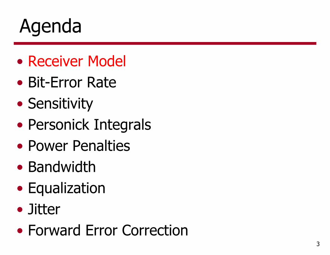
Agenda• Receiver Model• Bit-Error Rate• Sensitivity• Personick Integrals• Power Penalties• Bandwidth• Equalization• Jitter• Forward Error Correction
3
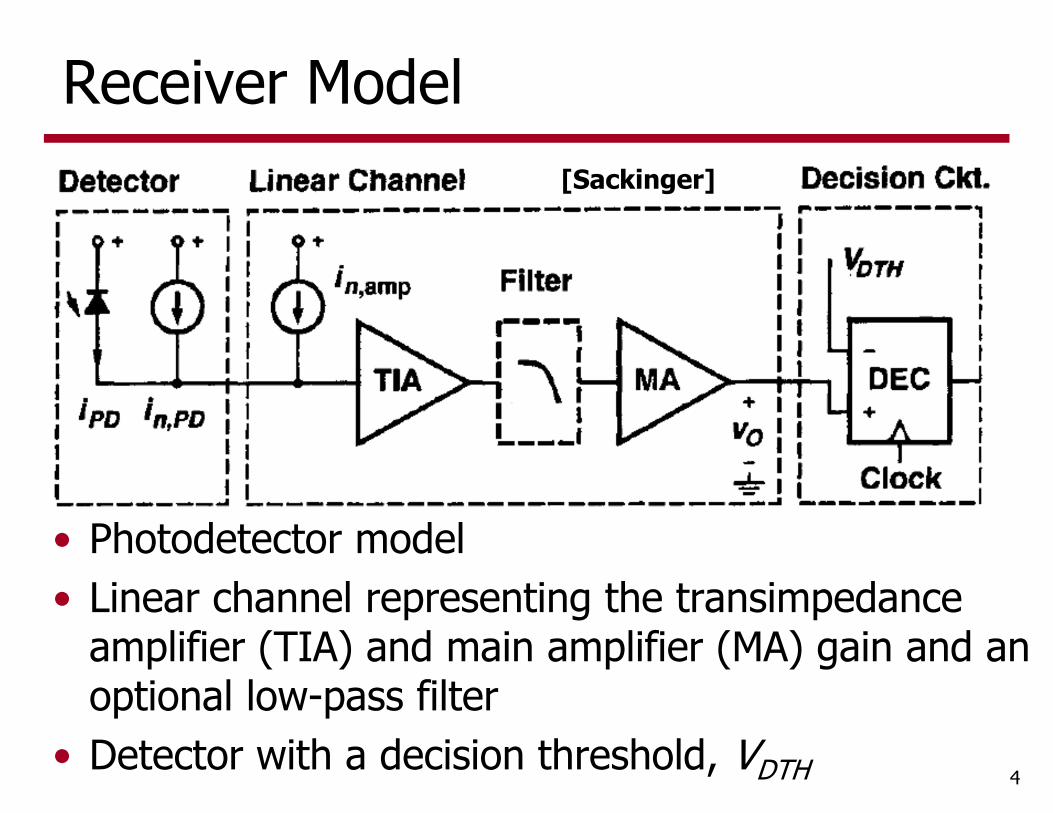
Receiver Model
4
• Photodetector model• Linear channel representing the transimpedance
amplifier (TIA) and main amplifier (MA) gain and an optional low-pass filter
• Detector with a decision threshold, VDTH
[Sackinger]
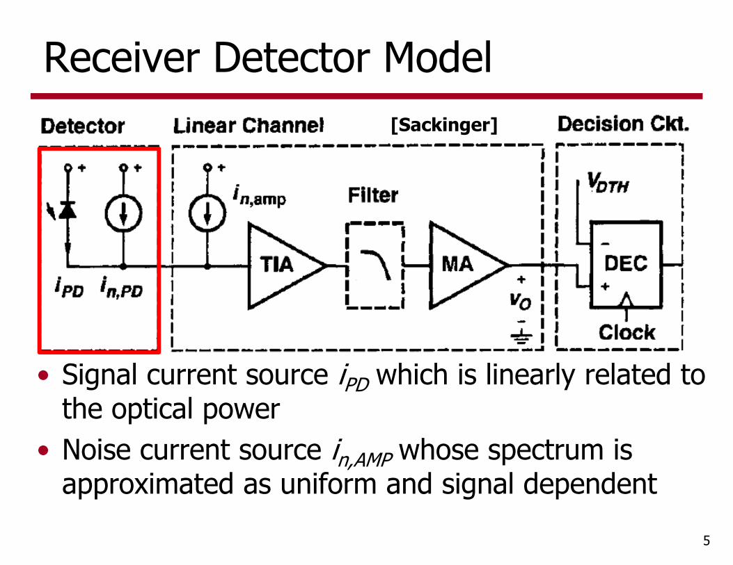
Receiver Detector Model
5
• Signal current source iPD which is linearly related to the optical power
• Noise current source in,AMP whose spectrum is approximated as uniform and signal dependent
[Sackinger]

Receiver Linear Channel (Front-End)
6
• Modeled with a linear transfer function H(f) relating the output voltage vOamplitude & phase with input current iPD• From a sensitivity perspective, the signals are small & linearity generally holds
• Single input-referred noise current source with a spectrum that produces the correct output-referred noise spectrum after passing through H(f)
• Generally, the TIA’s input-referred noise dominates
[Sackinger]
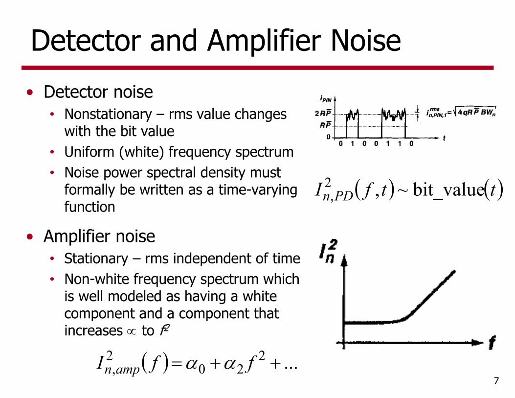
Detector and Amplifier Noise• Detector noise
• Nonstationary – rms value changes with the bit value
• Uniform (white) frequency spectrum• Noise power spectral density must
formally be written as a time-varying function
7
ttfI PDn bit_value~,2,
• Amplifier noise• Stationary – rms independent of time• Non-white frequency spectrum which
is well modeled as having a white component and a component that increases to f2
...220
2, ffI ampn
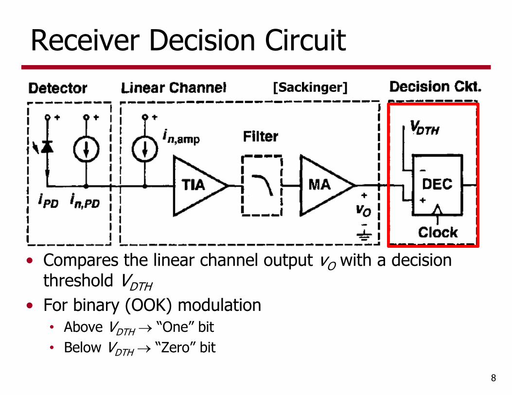
Receiver Decision Circuit
8
• Compares the linear channel output vO with a decision threshold VDTH
• For binary (OOK) modulation• Above VDTH “One” bit• Below VDTH “Zero” bit
[Sackinger]

Agenda• Receiver Model• Bit-Error Rate• Sensitivity• Personick Integrals• Power Penalties• Bandwidth• Equalization• Jitter• Forward Error Correction
9
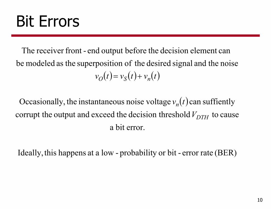
Bit Errors
10
(BER) rateerror -bitor y probabilit-low aat happens thisIdeally,
error.bit acause to hresholddecision t theexceed andoutput ecorrupt th
suffientlycan voltagenoise ousinstantane thely,Occasional
noise theand signal desired theofion superposit theas modeled becan element decision thebeforeoutput end-frontreceiver The
DTH
n
nSO
Vtv
tvtvtv
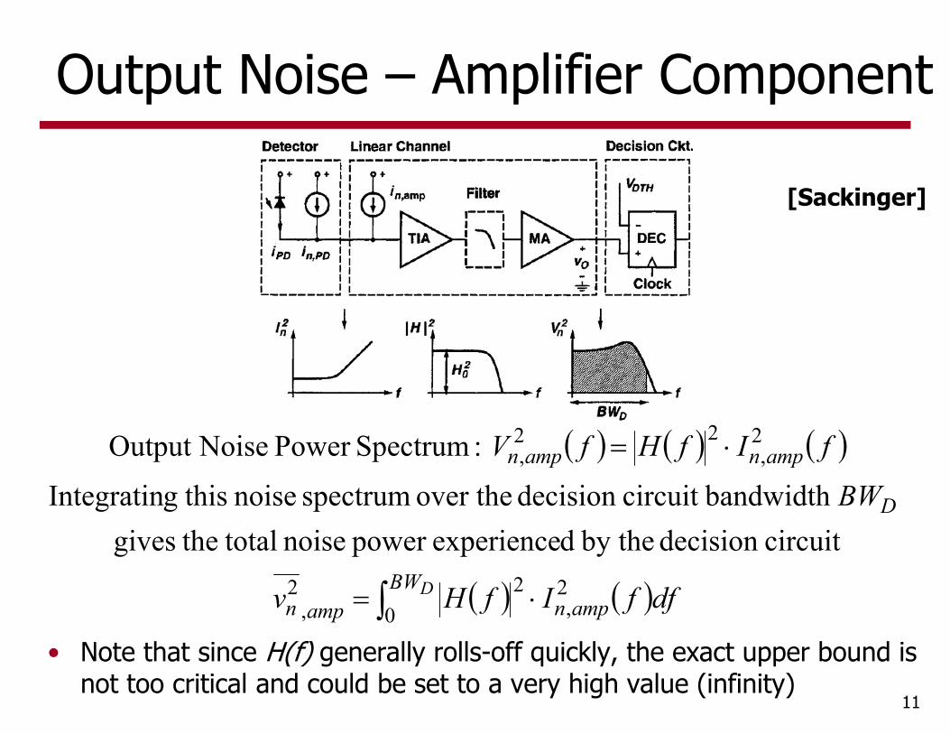
Output Noise – Amplifier Component
11
[Sackinger]
DBWampnampn
D
ampnampn
dffIfHv
BW
fIfHfV
02,
2,
2
2,
22,
circuitdecision by the dexperiencepower noise total thegives bandwidth circuit decision over the spectrum noise thisgIntegratin
:SpectrumPower NoiseOutput
• Note that since H(f) generally rolls-off quickly, the exact upper bound is not too critical and could be set to a very high value (infinity)
Output Noise – Detector Component
12
response. impulse end-front theis where
,,
asit writeshould weary,nonstation is noisedetector thebecause Formally,22
,2,
th
tdethttfIfHtfV tfjPDnPDn
• This effective convolution implies that the noise can impact not only it’s bits, but can also spread to impact other bits
• However, we generally assume that the noise varies slowly relate to h(t)and we can simplify the detector noise analysis
DBWPDntPDn
PDnPDn
dftfIfHv
tfIfHtfV
02,
2,
2
2,
22,
,
,,
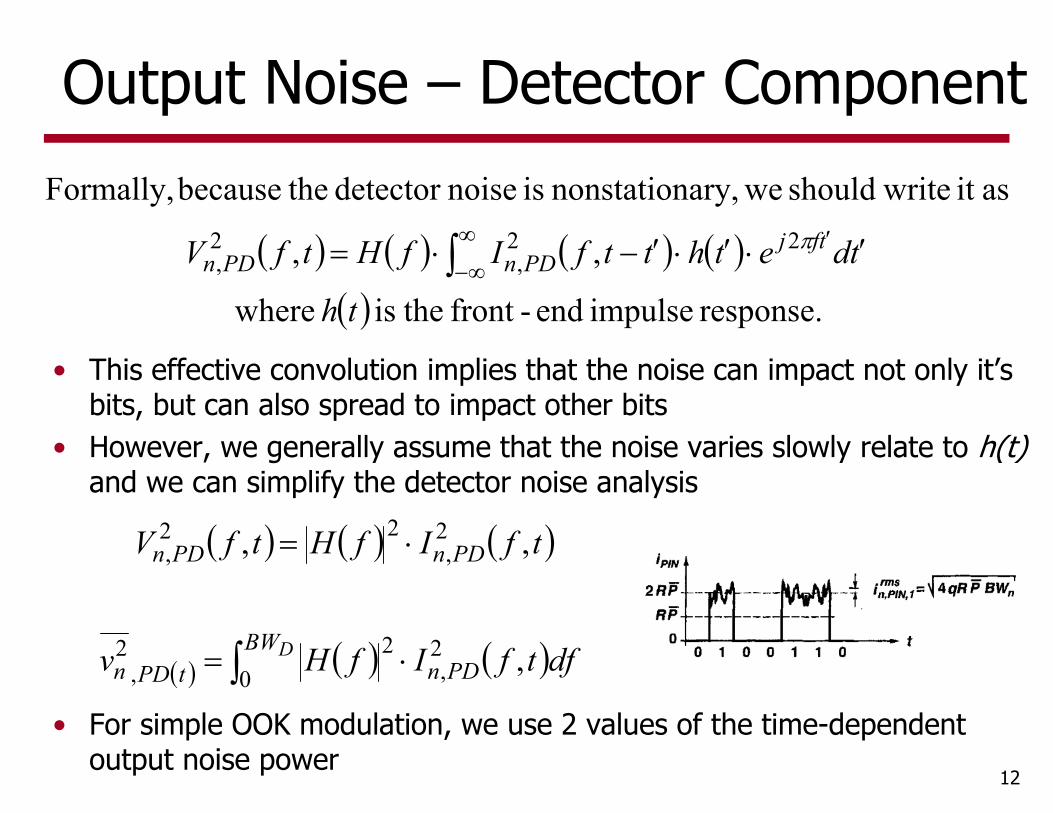
• For simple OOK modulation, we use 2 values of the time-dependent output noise power
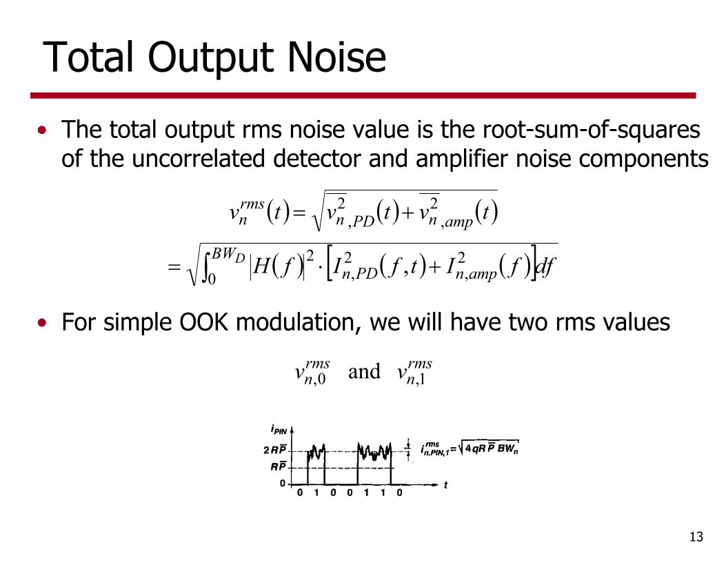
Total Output Noise
13
DBWampnPDn
ampnPDnrmsn
dffItfIfH
tvtvtv
02,
2,
2
,2
,2
,
• For simple OOK modulation, we will have two rms valuesrmsn
rmsn vv 1,0, and
• The total output rms noise value is the root-sum-of-squares of the uncorrelated detector and amplifier noise components

Signal, Noise, and Bit-Error Rate (BER)
14
• The noise is Gaussian with a standard deviation equal to the noise voltage rms value
• With an equal distribution of 1s and 0s, setting VDTH at the crossover of the two distributions yields the fewest bit errors
• The bit-error rate (BER) is defined as the probability that a 0 is misinterpreted as a 1 or vice-versa
[Sackinger]
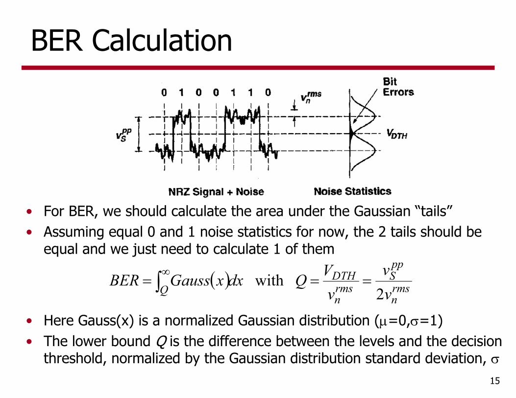
BER Calculation
15
• For BER, we should calculate the area under the Gaussian “tails”• Assuming equal 0 and 1 noise statistics for now, the 2 tails should be
equal and we just need to calculate 1 of them
rmsn
ppS
rmsn
DTHQ v
vv
VQdxxGaussBER2
with
• Here Gauss(x) is a normalized Gaussian distribution (=0,=1)• The lower bound Q is the difference between the levels and the decision
threshold, normalized by the Gaussian distribution standard deviation,
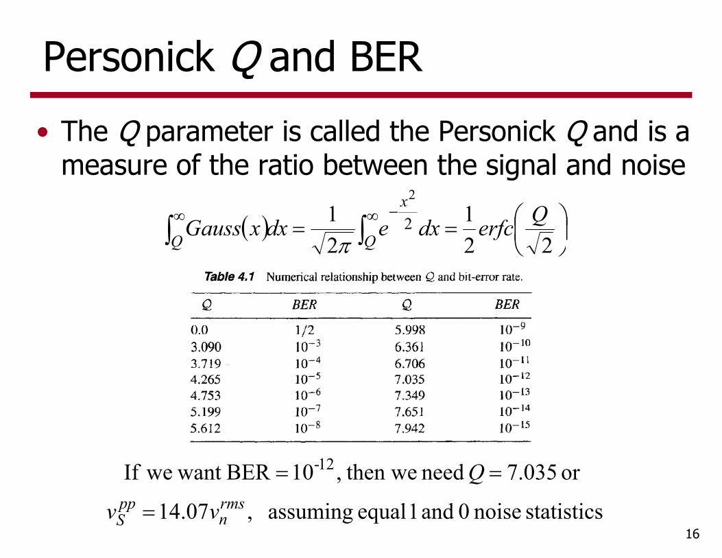
Personick Q and BER
16
• The Q parameter is called the Personick Q and is a measure of the ratio between the signal and noise
221
21 2
2QerfcdxedxxGauss
Q
x
Q
statistics noise 0 and 1 equal assuming ,07.14
or 035.7 need then we,10BER want weIf 12-
rmsn
ppS vv
Q
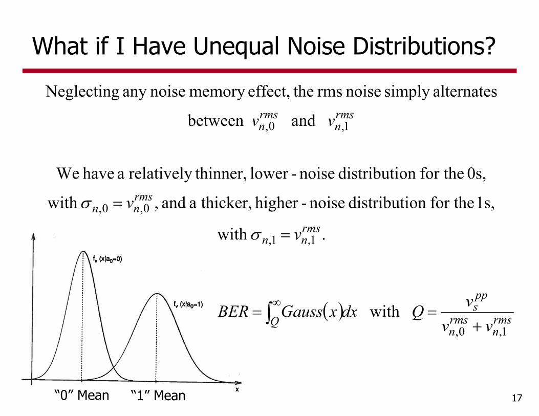
.with
1s, for theon distributi noise-higher thicker,a and ,with
0s, for theon distributi noise-lower thinner,relatively a have We
and between
alternatessimply noise rms theeffect,memory noiseany Neglecting
1,1,
0,0,
1,0,
rmsnn
rmsnn
rmsn
rmsn
v
v
vv
What if I Have Unequal Noise Distributions?
17
rmsn
rmsn
pps
Q vvvQdxxGaussBER
1,0, with
“0” Mean “1” Mean
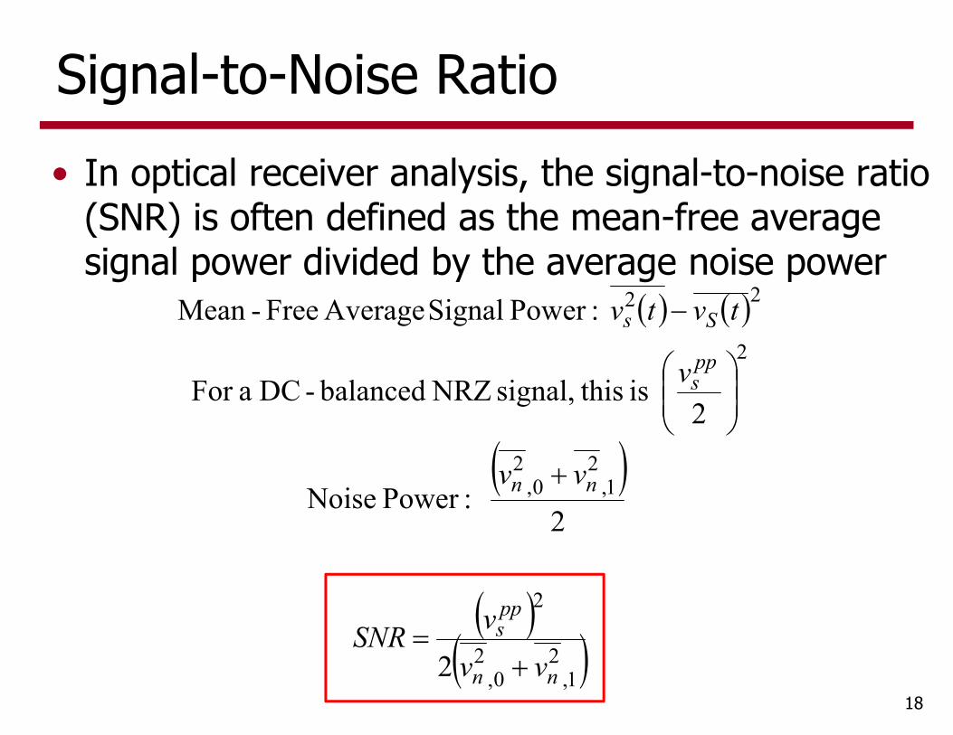
Signal-to-Noise Ratio
18
• In optical receiver analysis, the signal-to-noise ratio (SNR) is often defined as the mean-free average signal power divided by the average noise power
1,
20,
2
2
1,2
0,2
2
22
2
2
:Power Noise
2 is thissignal, NRZ balanced-DC aFor
:Power Signal Average Free-Mean
nn
pps
nn
pps
Ss
vvvSNR
vv
v
tvtv
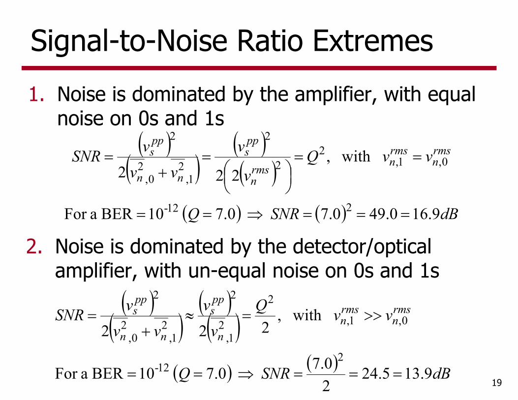
Signal-to-Noise Ratio Extremes
19
1. Noise is dominated by the amplifier, with equal noise on 0s and 1s
dBSNRQ
vvQv
vvv
vSNR rmsn
rmsn
rmsn
pps
nn
pps
9.160.490.7 0.7 10BER aFor
with ,222
212-
0,1,2
2
2
1,2
0,2
2
2. Noise is dominated by the detector/optical amplifier, with un-equal noise on 0s and 1s
dBSNRQ
vvQv
vvv
vSNR rmsn
rmsn
n
pps
nn
pps
9.135.2420.7 0.7 10BER aFor
with ,222
212-
0,1,
2
1,2
2
1,2
0,2
2

Agenda• Receiver Model• Bit-Error Rate• Sensitivity• Personick Integrals• Power Penalties• Bandwidth• Equalization• Jitter• Forward Error Correction
20
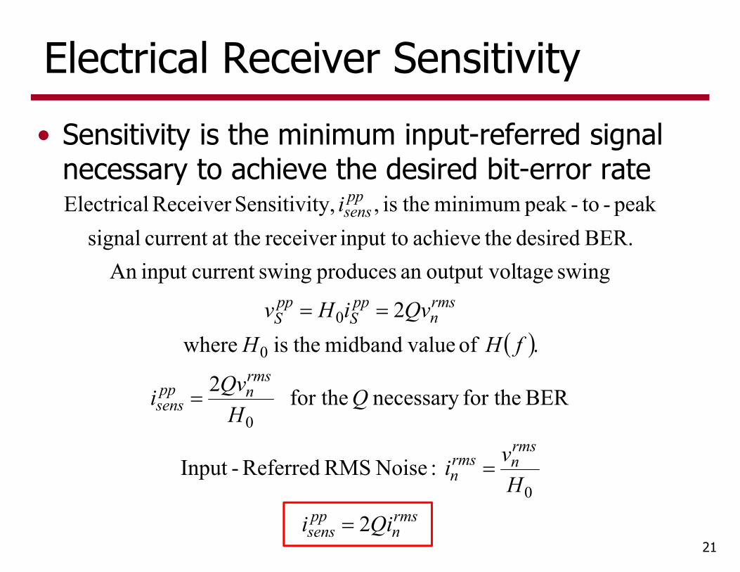
Electrical Receiver Sensitivity• Sensitivity is the minimum input-referred signal
necessary to achieve the desired bit-error rate
21
rmsn
ppsens
rmsnrms
n
rmsnpp
sens
rmsn
ppS
ppS
ppsens
Qii
Hvi
QH
Qvi
fHHQviHv
i
2
:Noise RMS Referred-Input
BER for thenecessary for the 2
. of valuemidband theis where2
swing tageoutput volan produces swingcurrent input An BER. desired theachieve input toreceiver at thecurrent signal
peak-to-peak minimum theis , y,SensitivitReceiver Electrical
0
0
0
0
22
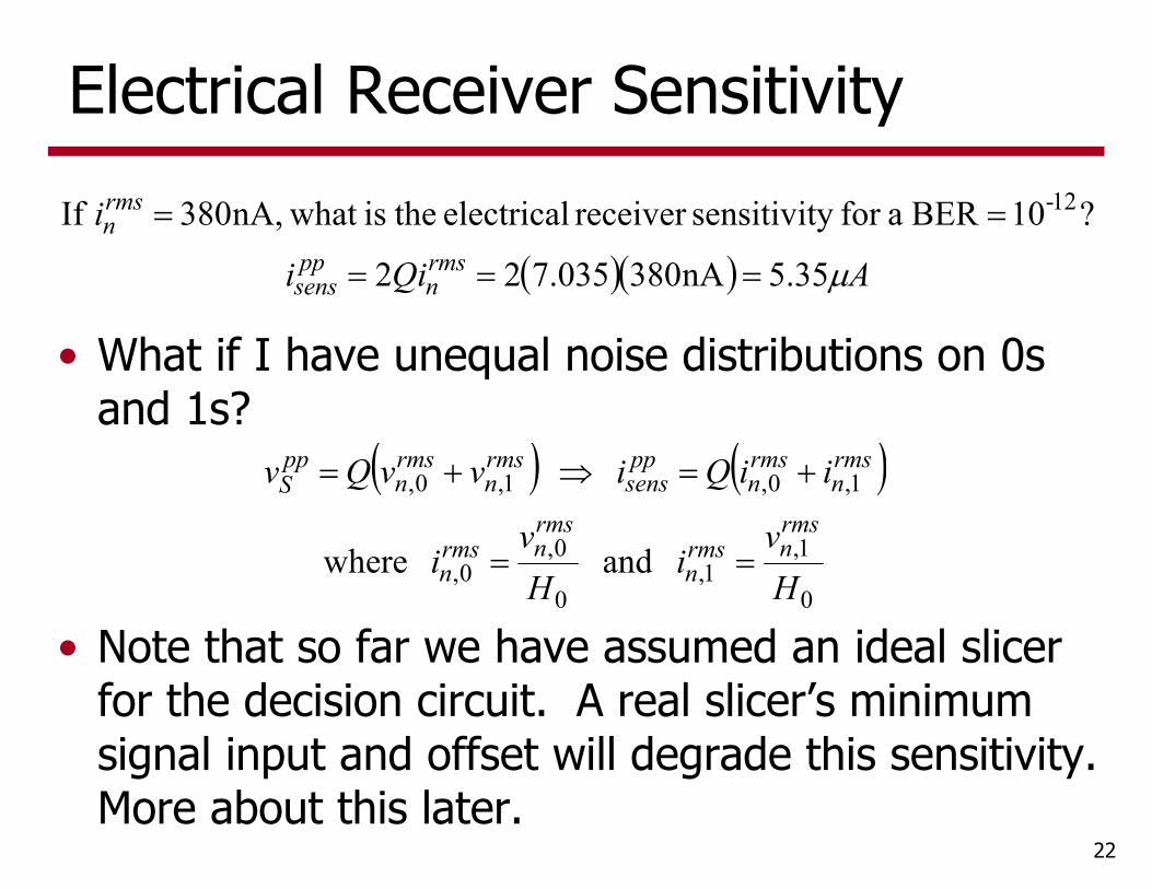
AQii
irmsn
ppsens
rmsn
35.5nA380035.722
?10BER afor y sensitivitreceiver electrical theis what nA,380 If 12-
Electrical Receiver Sensitivity
• What if I have unequal noise distributions on 0s and 1s?
0
1,1,
0
0,0,
1,0,1,0,
and where
Hv
iH
vi
iiQivvQvrmsnrms
n
rmsnrms
n
rmsn
rmsn
ppsens
rmsn
rmsn
ppS
• Note that so far we have assumed an ideal slicer for the decision circuit. A real slicer’s minimum signal input and offset will degrade this sensitivity. More about this later.
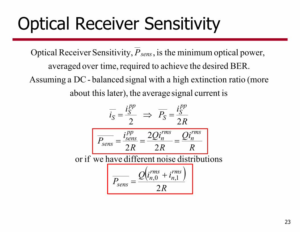
Optical Receiver Sensitivity
23
R
iiQP
RQi
RQi
RiP
RiPii
P
rmsn
rmsn
sens
rmsn
rmsn
ppsens
sens
ppS
S
ppS
S
sens
2
onsdistributi noisedifferent have weifor 2
22
2
2
iscurrent signal average thelater), about this(more ratio extinctionhigh a with signal balanced-DC a Assuming
BER. desired theachieve torequired over time, averaged power, optical minimum theis , y,SensitivitReceiver Optical
1,0,

24
dBmWWAR
QiP
WARi
rmsn
sens
rmsn
8.2434.3/8.0
nA380035.7
?10BER afor y sensitivit
receiver optical theis what ,/8.0 andnA 380 If12-
Optical Receiver Sensitivity
• Note that the optical receiver sensitivity is based on the average signal value, whereas the electrical sensitivity is based on the peak-to-peak signal value
25
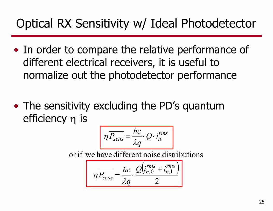
Optical RX Sensitivity w/ Ideal Photodetector
• In order to compare the relative performance of different electrical receivers, it is useful to normalize out the photodetector performance
• The sensitivity excluding the PD’s quantum efficiency is
2
onsdistributi noisedifferent have weifor
1,0,rmsn
rmsn
sens
rmsnsens
iiQq
hcP
iQq
hcP

26
dBmWWAR
QiP
WARi
rmsn
sens
rmsn
8.2434.3/8.0
nA380035.7
?10BER afor y sensitivit
receiver optical theis what ,/8.0 andnA 380 If12-
Optical RX Sensitivity w/ Ideal Photodetector
• Previous example using PD with R=0.8A/W
• Now, normalizing (multiplying) by the quantum efficiency or dividing by an ideal responsivity at a given wavelength
dBmWWnmmWA
Qiq
hcP
i
rmsnsens
rmsn
7.2616.224.1
67.21550108nA380035.7
tor?photodetec idealan with 10BER afor y sensitivitreceiver optical theiswhat
1550nm, of wavelenthaat operating are weandnA 380 If
5
12-
27
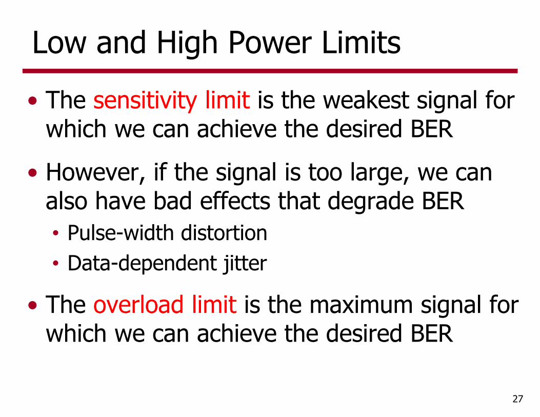
Low and High Power Limits• The sensitivity limit is the weakest signal for
which we can achieve the desired BER• However, if the signal is too large, we can
also have bad effects that degrade BER• Pulse-width distortion• Data-dependent jitter
• The overload limit is the maximum signal for which we can achieve the desired BER
28
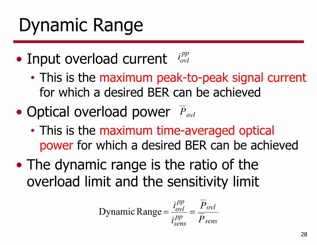
Dynamic Range• Input overload current
• This is the maximum peak-to-peak signal current for which a desired BER can be achieved
• Optical overload power• This is the maximum time-averaged optical
power for which a desired BER can be achieved• The dynamic range is the ratio of the
overload limit and the sensitivity limit
ppovli
ovlP
sens
ovlppsens
ppovl
PP
ii
Range Dynamic
29
following for the /8.0 andnA 380 Assuming WARirmsn
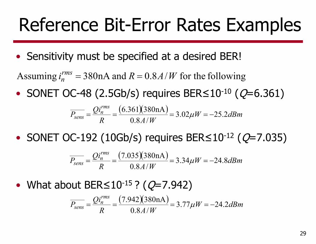
Reference Bit-Error Rates Examples
• SONET OC-48 (2.5Gb/s) requires BER≤10-10 (Q=6.361) dBmW
WARQiP
rmsn
sens 2.2502.3/8.0
nA380361.6
• SONET OC-192 (10Gb/s) requires BER≤10-12 (Q=7.035) dBmW
WARQiP
rmsn
sens 8.2434.3/8.0
nA380035.7
• What about BER≤10-15 ? (Q=7.942) dBmW
WARQiP
rmsn
sens 2.2477.3/8.0
nA380942.7
• Sensitivity must be specified at a desired BER!
30
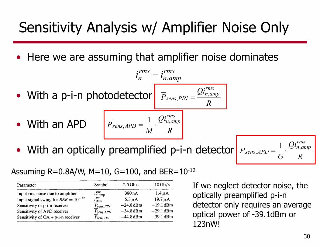
Sensitivity Analysis w/ Amplifier Noise Only
• With a p-i-n photodetectorR
QiP
rmsampn
PINsens,
,
• With an APD
• With an optically preamplified p-i-n detector
• Here we are assuming that amplifier noise dominatesrms
ampnrmsn ii ,
RQi
MP
rmsampn
APDsens,
,1
RQi
GP
rmsampn
APDsens,
,1
Assuming R=0.8A/W, M=10, G=100, and BER=10-12
If we neglect detector noise, the optically preamplified p-i-n detector only requires an average optical power of -39.1dBm or 123nW!
31
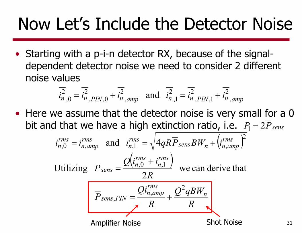
Now Let’s Include the Detector Noise
• Here we assume that the detector noise is very small for a 0 bit and that we have a high extinction ratio, i.e.
• Starting with a p-i-n detector RX, because of the signal-dependent detector noise we need to consider 2 different noise values
ampnPINnnampnPINnn iiiiii ,2
1,,2
1,2
,2
0,,2
0,2 and
sensPP 21
RqBWQ
RQi
P
RiiQ
P
iBWPqRiii
nrms
ampnPINsens
rmsn
rmsn
sens
rmsampnnsens
rmsn
rmsampn
rmsn
2,
,
1,0,
2,1,,0,
that derivecan we2
Utilizing
4 and
Amplifier Noise Shot Noise
32
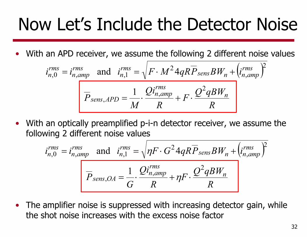
Now Let’s Include the Detector Noise• With an APD receiver, we assume the following 2 different noise values
RqBWQF
RQi
MP
iBWPqRMFiii
nrms
ampnAPDsens
rmsampnnsens
rmsn
rmsampn
rmsn
2,
,
2,
21,,0,
1
4 and
• With an optically preamplified p-i-n detector receiver, we assume the following 2 different noise values
RqBWQF
RQi
GP
iBWPqRGFiii
nrms
ampnOAsens
rmsampnnsens
rmsn
rmsampn
rmsn
2,
,
2,
21,,0,
1
4 and
• The amplifier noise is suppressed with increasing detector gain, while the shot noise increases with the excess noise factor
33
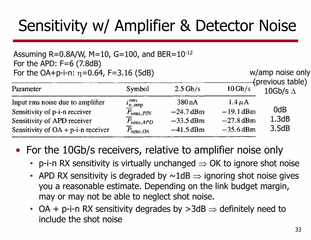
Sensitivity w/ Amplifier & Detector NoiseAssuming R=0.8A/W, M=10, G=100, and BER=10-12
For the APD: F=6 (7.8dB) For the OA+p-i-n: =0.64, F=3.16 (5dB) w/amp noise only
(previous table)10Gb/s
0dB1.3dB3.5dB
• For the 10Gb/s receivers, relative to amplifier noise only • p-i-n RX sensitivity is virtually unchanged OK to ignore shot noise• APD RX sensitivity is degraded by ~1dB ignoring shot noise gives
you a reasonable estimate. Depending on the link budget margin, may or may not be able to neglect shot noise.
• OA + p-i-n RX sensitivity degrades by >3dB definitely need to include the shot noise
34
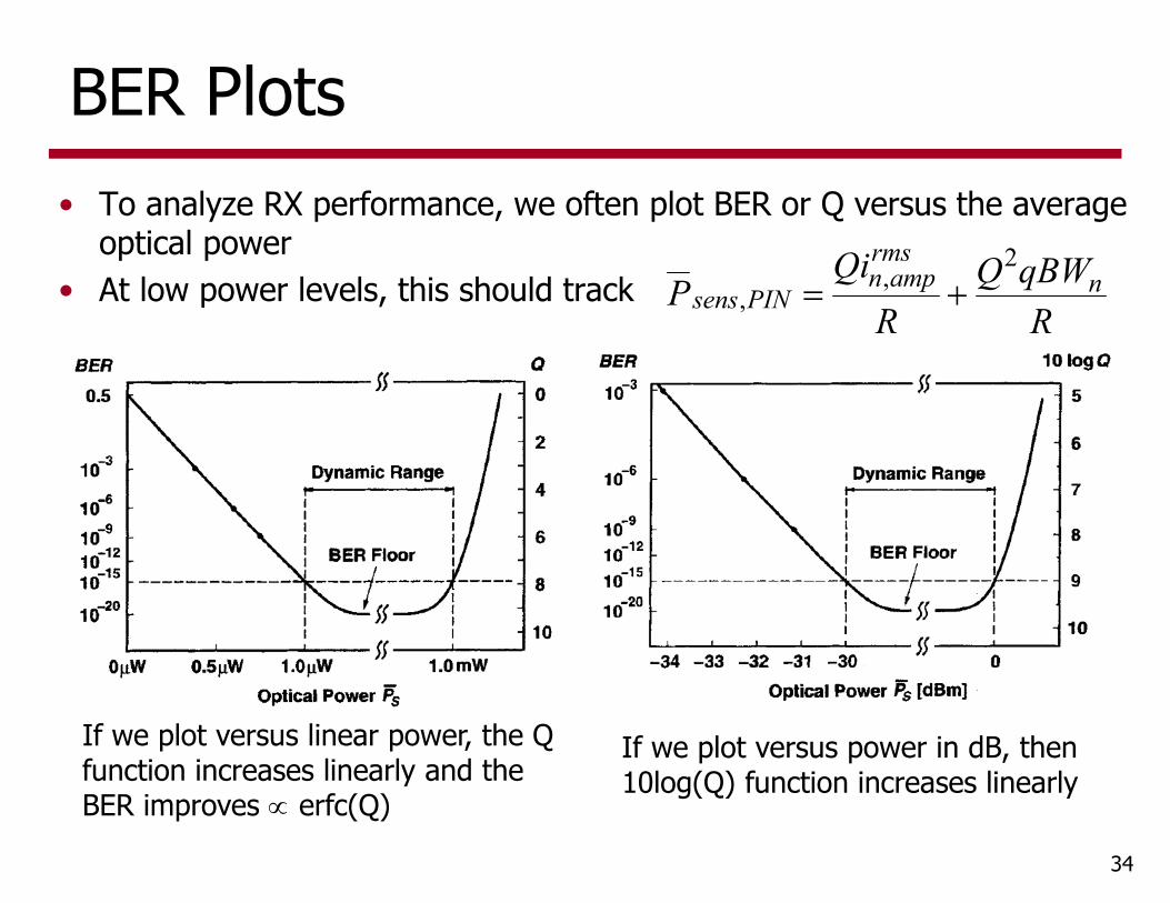
BER Plots• To analyze RX performance, we often plot BER or Q versus the average
optical power• At low power levels, this should track
RqBWQ
RQi
P nrms
ampnPINsens
2,
,
If we plot versus linear power, the Q function increases linearly and the BER improves erfc(Q)
If we plot versus power in dB, then 10log(Q) function increases linearly
35
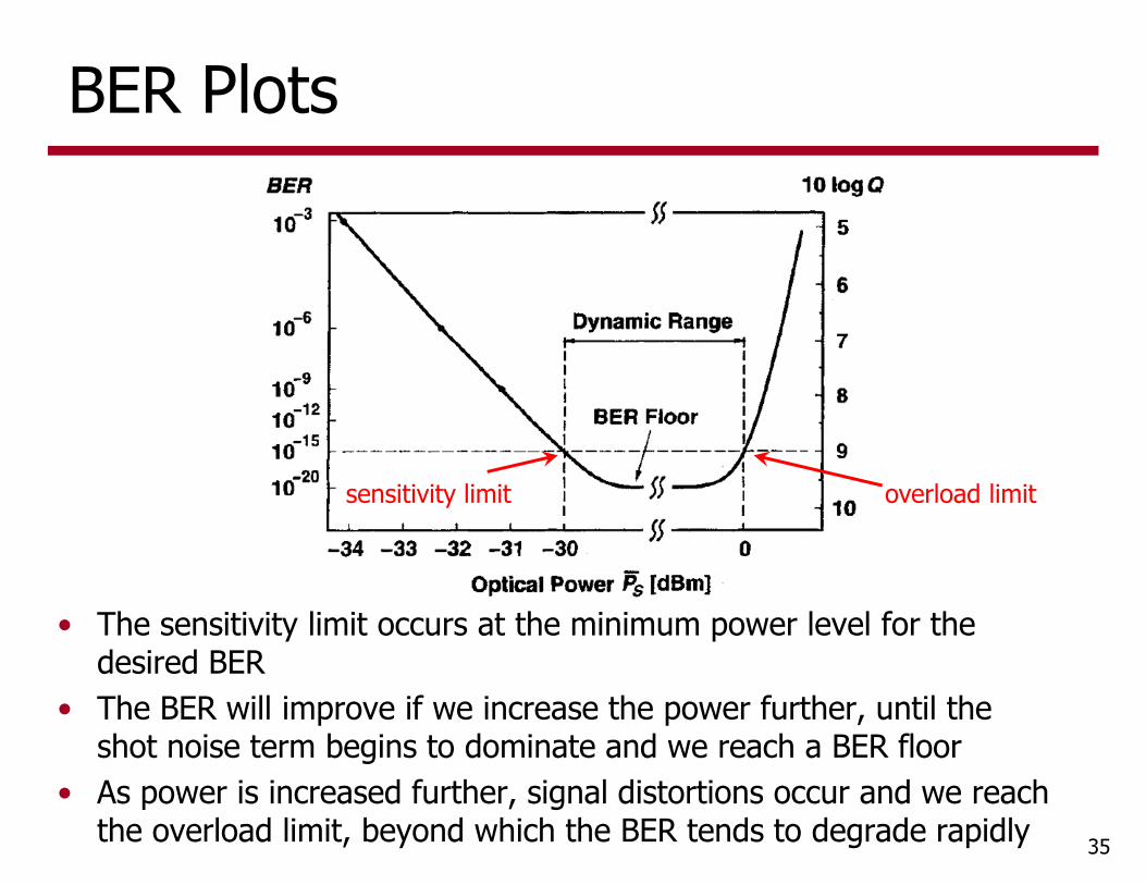
BER Plots
• The sensitivity limit occurs at the minimum power level for the desired BER
• The BER will improve if we increase the power further, until the shot noise term begins to dominate and we reach a BER floor
• As power is increased further, signal distortions occur and we reach the overload limit, beyond which the BER tends to degrade rapidly
sensitivity limit overload limit
36
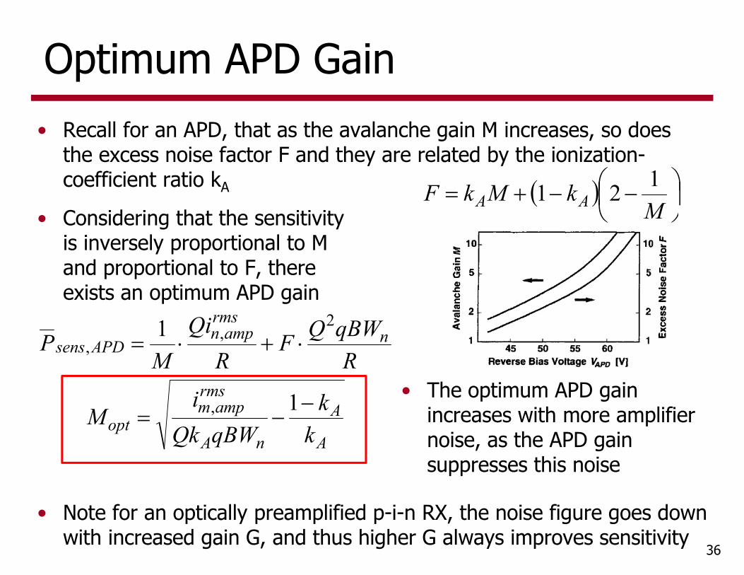
Optimum APD Gain• Recall for an APD, that as the avalanche gain M increases, so does
the excess noise factor F and they are related by the ionization-coefficient ratio kA
MkMkF AA
121• Considering that the sensitivity
is inversely proportional to M and proportional to F, there exists an optimum APD gain
A
A
nA
rmsampm
opt
nrms
ampnAPDsens
kk
qBWQki
M
RqBWQF
RQi
MP
1
1
,
2,
,
• The optimum APD gain increases with more amplifier noise, as the APD gain suppresses this noise
• Note for an optically preamplified p-i-n RX, the noise figure goes down with increased gain G, and thus higher G always improves sensitivity
37
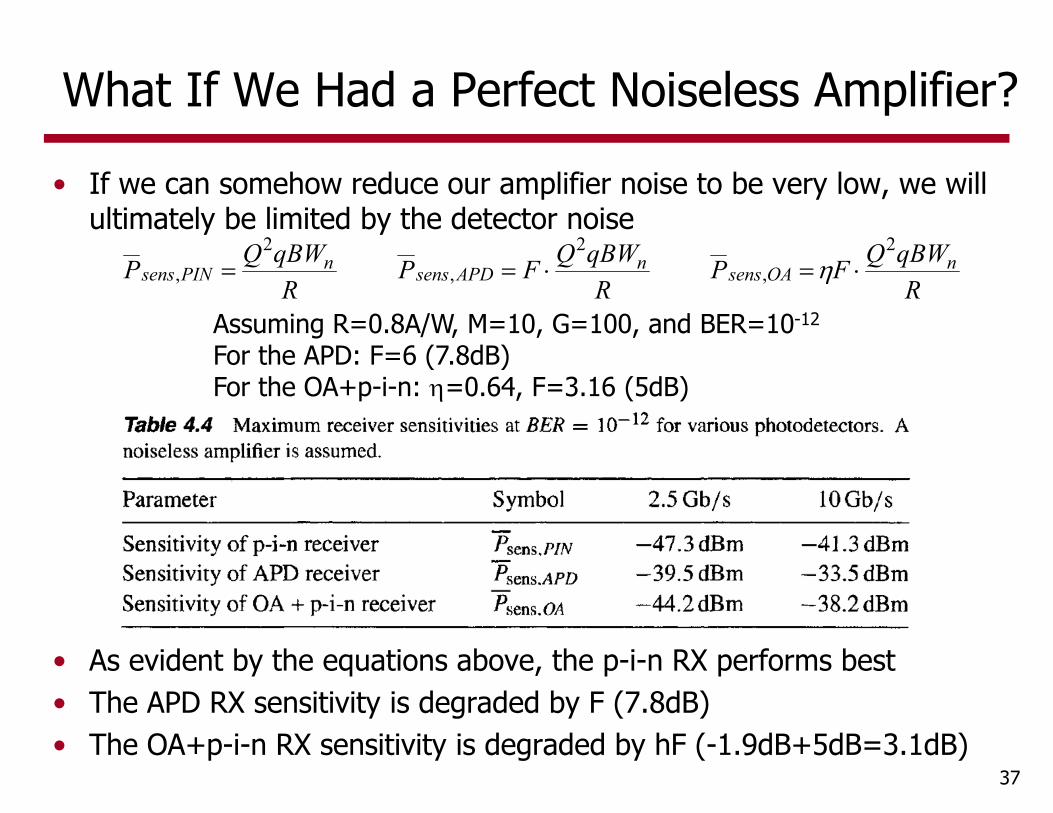
What If We Had a Perfect Noiseless Amplifier?
• If we can somehow reduce our amplifier noise to be very low, we will ultimately be limited by the detector noise
RqBWQP nPINsens
2,
RqBWQFP nAPDsens
2,
RqBWQFP nOAsens
2,
Assuming R=0.8A/W, M=10, G=100, and BER=10-12
For the APD: F=6 (7.8dB) For the OA+p-i-n: =0.64, F=3.16 (5dB)
• As evident by the equations above, the p-i-n RX performs best• The APD RX sensitivity is degraded by F (7.8dB)• The OA+p-i-n RX sensitivity is degraded by hF (-1.9dB+5dB=3.1dB)
38
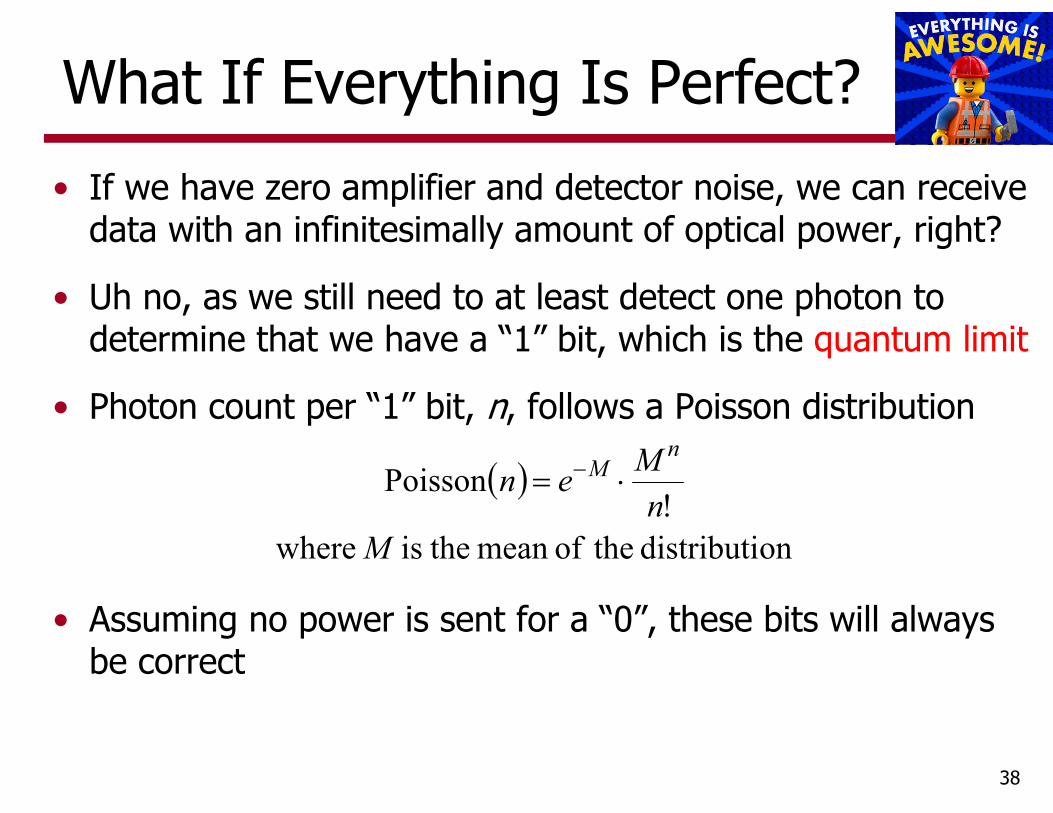
What If Everything Is Perfect?• If we have zero amplifier and detector noise, we can receive
data with an infinitesimally amount of optical power, right?
• Uh no, as we still need to at least detect one photon to determine that we have a “1” bit, which is the quantum limit
• Photon count per “1” bit, n, follows a Poisson distribution
ondistributi theofmean theis where!
Poisson
Mn
Menn
M
• Assuming no power is sent for a “0”, these bits will always be correct
39
Quantum Limit Sensitivity• The error probability for a “1” is Poisson(0)
ratebit theis where 22ln
ofpower averagean in results which photons, 2 need webit,Per 2ln
bit "1"per photons ofnumber averagean need weThus,210Poisson
21
, BBhcBERP
MBERM
M
eBER
quantsens
M
• How do the previous example RX sensitivities with amplifier and detector noise compare relative to the 10Gb/s quantum limit sensitivity?• p-i-n RX = +28.5dB• APD RX = +19.8dB• OA + p-i-n = +12dB
Agenda• Receiver Model• Bit-Error Rate• Sensitivity• Personick Integrals• Power Penalties• Bandwidth• Equalization• Jitter• Forward Error Correction
40
41
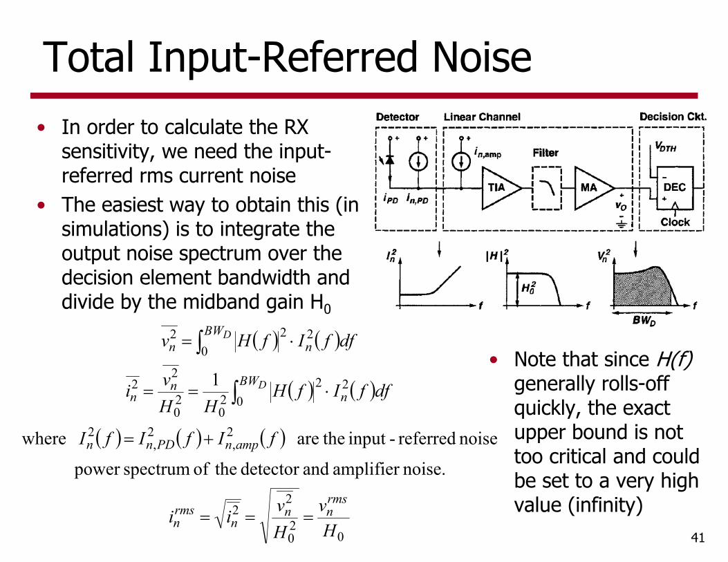
Total Input-Referred Noise• In order to calculate the RX
sensitivity, we need the input-referred rms current noise
• The easiest way to obtain this (in simulations) is to integrate the output noise spectrum over the decision element bandwidth and divide by the midband gain H0
020
22
2,
2,
2
022
20
20
22
0222
noise.amplifier anddetector theof spectrumpower
noise referred-input theare where
1
Hv
Hvii
fIfIfI
dffIfHHH
vi
dffIfHv
rmsnn
nrmsn
ampnPDnn
BWn
nn
BWnn
D
D
• Note that since H(f)generally rolls-off quickly, the exact upper bound is not too critical and could be set to a very high value (infinity)
42
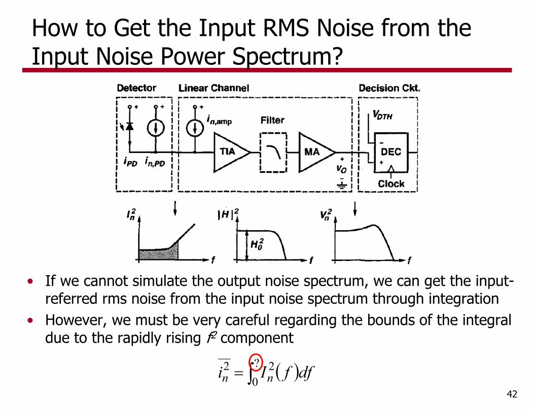
How to Get the Input RMS Noise from the Input Noise Power Spectrum?
• If we cannot simulate the output noise spectrum, we can get the input-referred rms noise from the input noise spectrum through integration
• However, we must be very careful regarding the bounds of the integral due to the rapidly rising f2 component
?0
22 dffIi nn
43
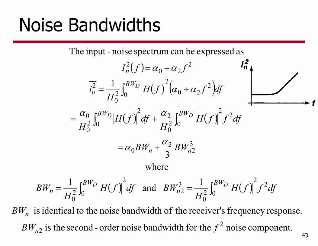
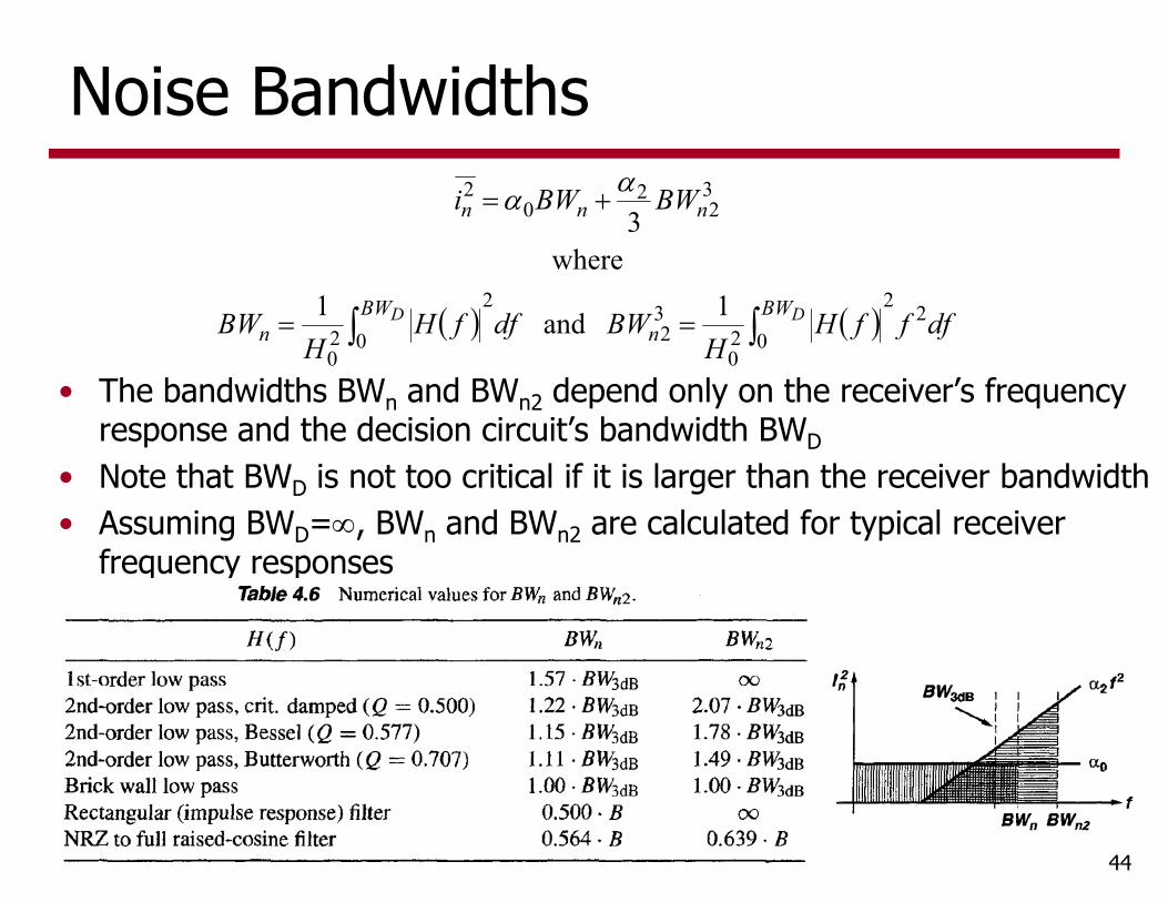
Noise Bandwidths
component. noise for thebandwidth noiseorder -second theis
response.frequency sreceiver' theofbandwidth noise the toidentical is
1 and 1where
3
1
as expressed becan spectrum noise-input The
22
22
020
32
2
020
32
20
22
020
22
020
0
220
2
020
2
220
2
fBW
BW
dfffHH
BWdffHH
BW
BWBW
dfffHH
dffHH
dfffHH
i
ffI
n
n
BWn
BWn
nn
BWBW
BWn
n
DD
DD
D
44
Noise Bandwidths
dfffHH
BWdffHH
BW
BWBWi
DD BWn
BWn
nnn
22
020
32
2
020
32
20
2
1 and 1where
3
• The bandwidths BWn and BWn2 depend only on the receiver’s frequency response and the decision circuit’s bandwidth BWD
• Note that BWD is not too critical if it is larger than the receiver bandwidth• Assuming BWD=, BWn and BWn2 are calculated for typical receiver
frequency responses
45
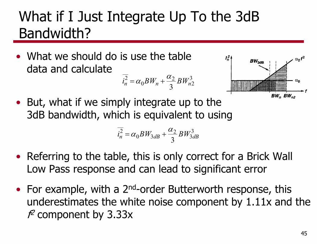
What if I Just Integrate Up To the 3dB Bandwidth?
32
20
2
3 nnn BWBWi
• What we should do is use the table data and calculate
• But, what if we simply integrate up to the 3dB bandwidth, which is equivalent to using
33
230
2
3 dBdBn BWBWi
• Referring to the table, this is only correct for a Brick Wall Low Pass response and can lead to significant error
• For example, with a 2nd-order Butterworth response, this underestimates the white noise component by 1.11x and the f2 component by 3.33x
46
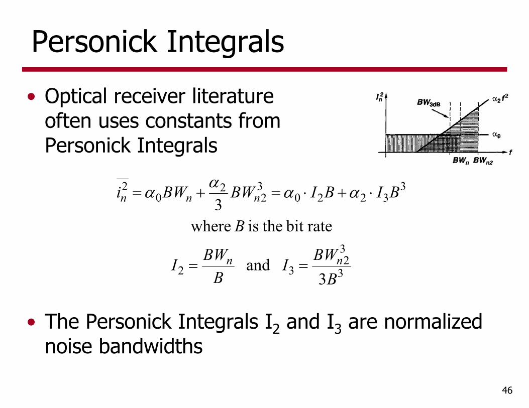
Personick Integrals
3
32
32
33220
32
20
2
3 and
ratebit theis where3
BBWI
BBWI
B
BIBIBWBWi
nn
nnn
• Optical receiver literature often uses constants from Personick Integrals
• The Personick Integrals I2 and I3 are normalized noise bandwidths
Agenda• Receiver Model• Bit-Error Rate• Sensitivity• Personick Integrals• Power Penalties• Bandwidth• Equalization• Jitter• Forward Error Correction
47
48
Power Penalty• So far we have primarily been considering random
noise sources and assumed that we have had an ideal transmitter, receiver decision circuit, etc…
• The actual receiver sensitivity will be degraded by impairments throughout the optical link and is quantified by power penalties
• The power penalty PP is the increase in average transmit power necessary to maintain the desired BER, relative to an ideal case where we don’t have the impairment
• This is quantified in dBs, 10log(PP)
49
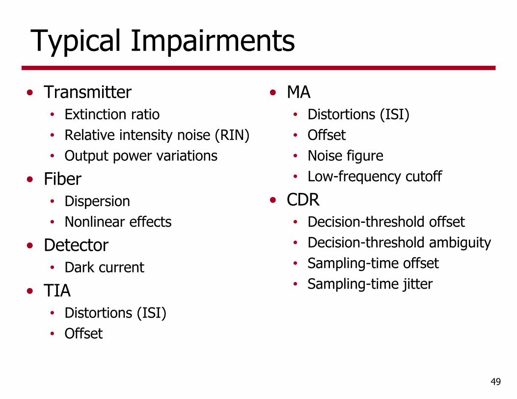
Typical Impairments • Transmitter
• Extinction ratio• Relative intensity noise (RIN)• Output power variations
• Fiber• Dispersion• Nonlinear effects
• Detector• Dark current
• TIA• Distortions (ISI)• Offset
• MA• Distortions (ISI)• Offset• Noise figure• Low-frequency cutoff
• CDR• Decision-threshold offset• Decision-threshold ambiguity• Sampling-time offset• Sampling-time jitter
50
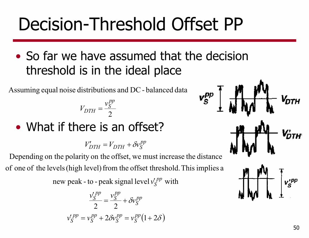
Decision-Threshold Offset PP• So far we have assumed that the decision
threshold is in the ideal place
2
data balanced-DC and onsdistributi noise equal AssumingppS
DTHvV
• What if there is an offset?
21222
with level signalpeak -to-peak new
a implies This eshold.offset thr thefrom level)(high levels theof one ofdistance theincreasemust weoffset, on thepolarity on the Depending
ppS
ppS
ppS
ppS
ppS
ppS
ppS
ppS
ppSDTHDTH
vvvv
vvv
v
vVV
51
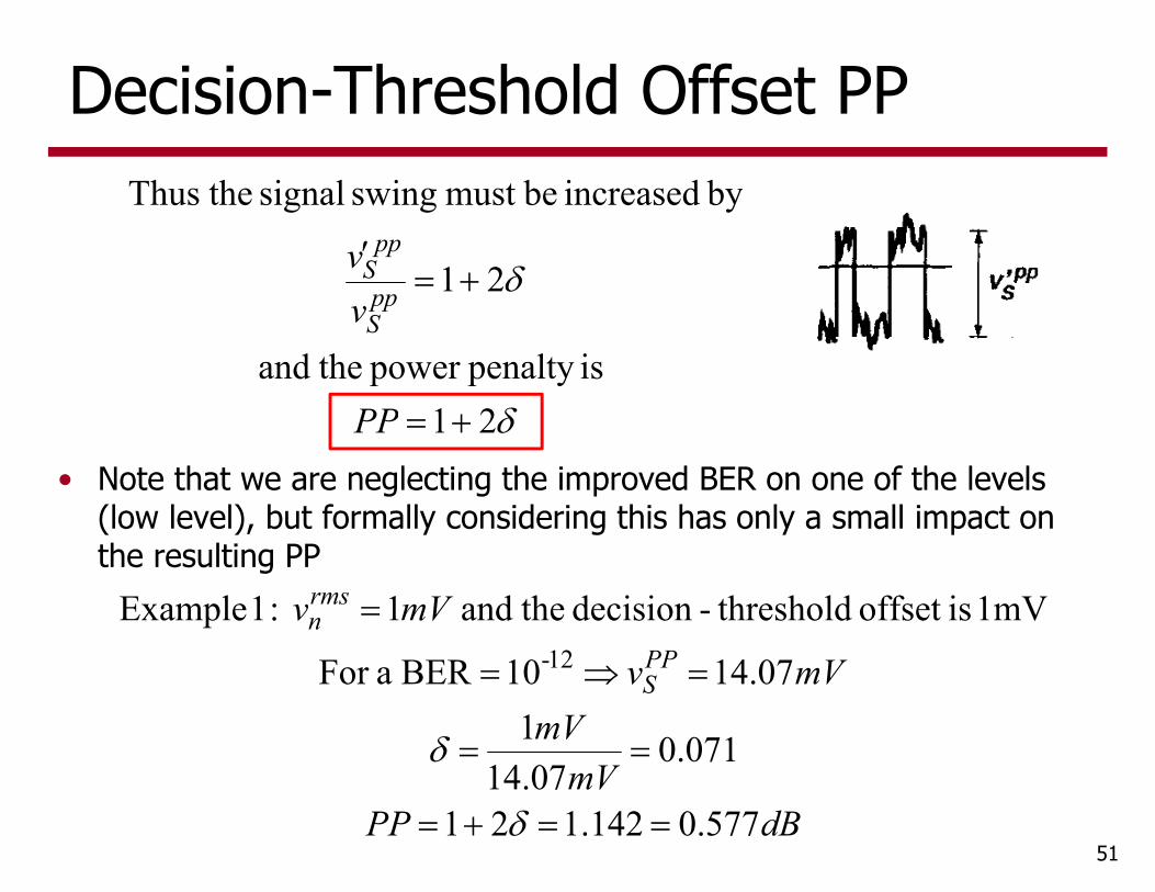
Decision-Threshold Offset PP
21 ispenalty power theand
21
by increased bemust swing signal theThus
PP
vv
ppS
ppS
dBPPmV
mVmVv
mVvPPS
rmsn
577.0142.121
071.007.14
107.1410BER aFor
1mV isoffset threshold-decision theand 1 :1 Example12-
• Note that we are neglecting the improved BER on one of the levels (low level), but formally considering this has only a small impact on the resulting PP
52
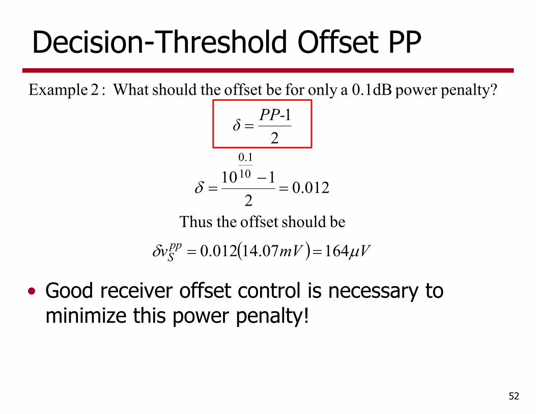
Decision-Threshold Offset PP
VmVv
PP-δ
ppS
16407.14012.0
be shouldoffset theThus
012.02
110
21
penalty?power 0.1dB aonly for beoffset theshould What :2 Example
101.0
• Good receiver offset control is necessary to minimize this power penalty!
53
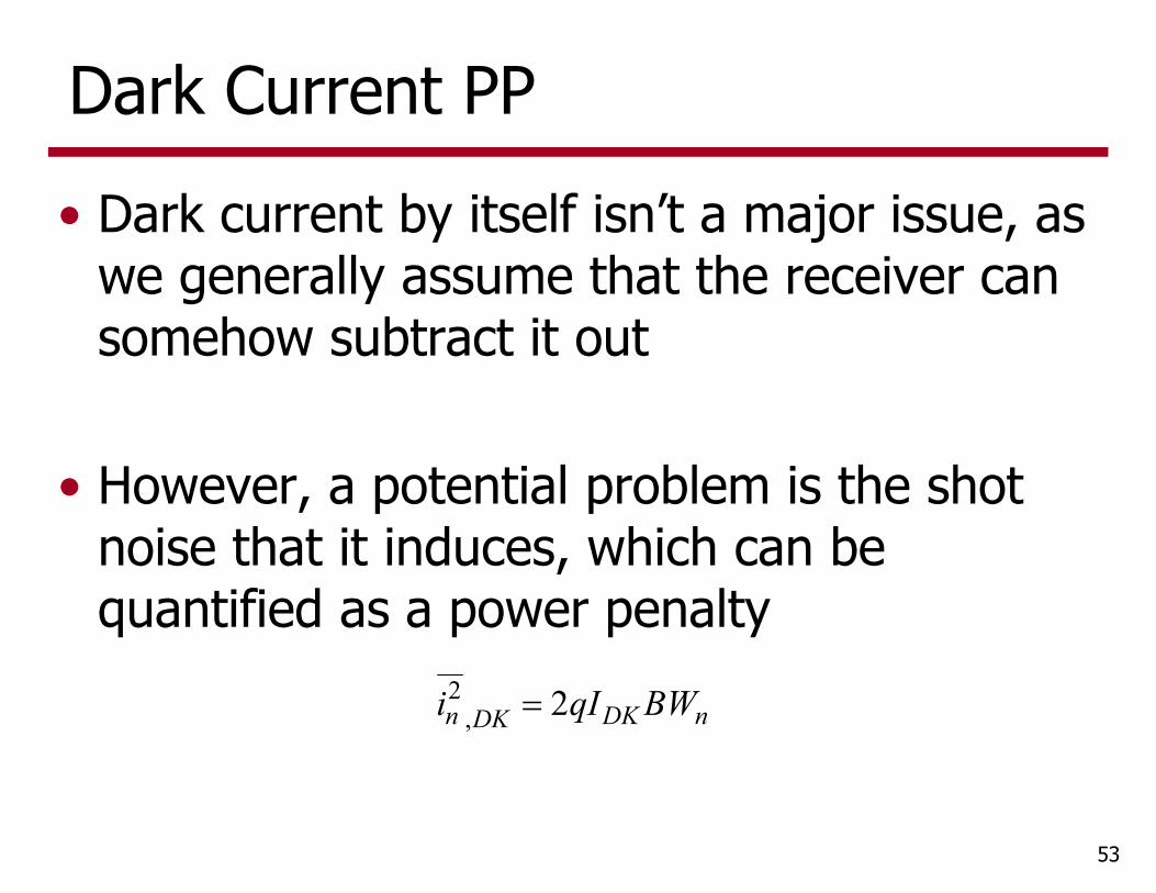
Dark Current PP• Dark current by itself isn’t a major issue, as
we generally assume that the receiver can somehow subtract it out
• However, a potential problem is the shot noise that it induces, which can be quantified as a power penalty
nDKDKn BWqIi 2,2
54
Dark Current PP• To keep things simple, let’s assume that the
receiver noise is dominated by the amplifier noise. Note, this will slightly overestimate the dark current PP.
• The dark current noise increases the total noise by
ampn
nDK
rmsn
ampn
nDK
ampn
DKnampn
iBWqIPP
i
iBWqI
i
ii
,2
,2
,2
,2
,2
21
toalproportion isy sensitivit theAs
21
55
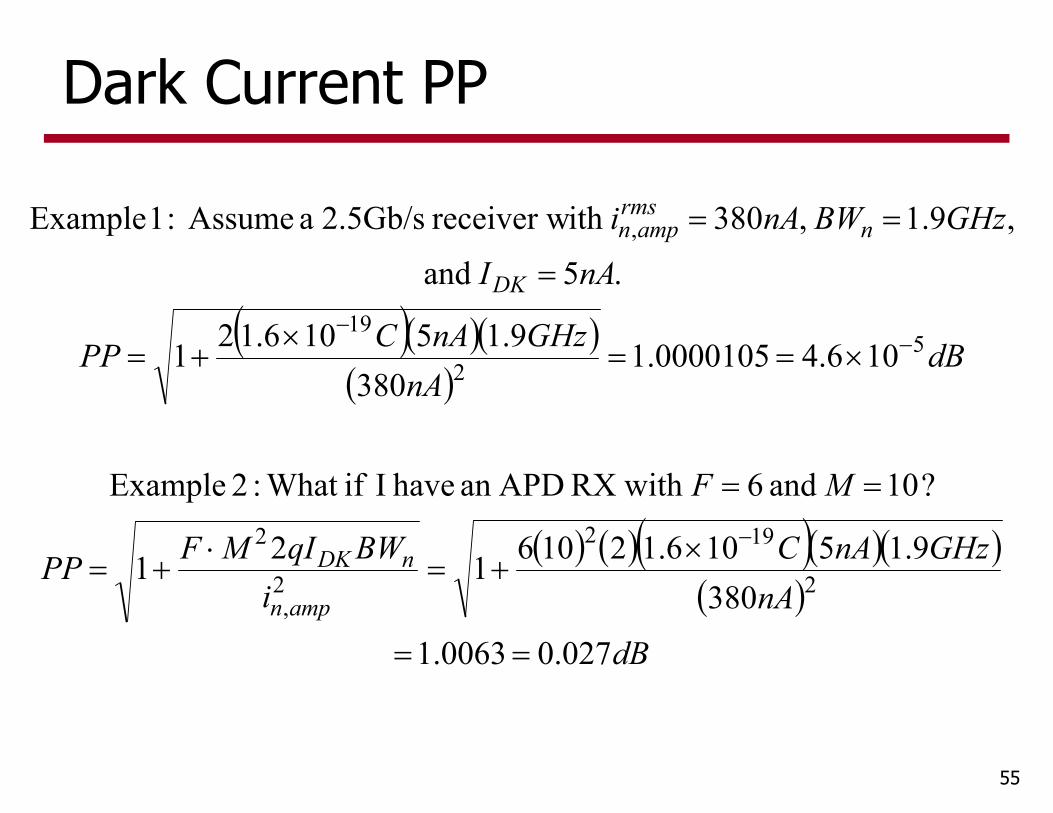
Dark Current PP
dB
nAGHznAC
iBWqIMFPP
MF
dBnA
GHznACPP
nAI
GHzBWnAi
ampn
nDK
DK
nrms
ampn
027.00063.1
3809.15106.12106121
?10 and 6 with RX APDan have I if What :2 Example
106.40000105.1380
9.15106.121
.5 and
,9.1 ,380ith receiver w 2.5Gb/s a Assume :1 Example
2
192
2,
2
52
19
,
56
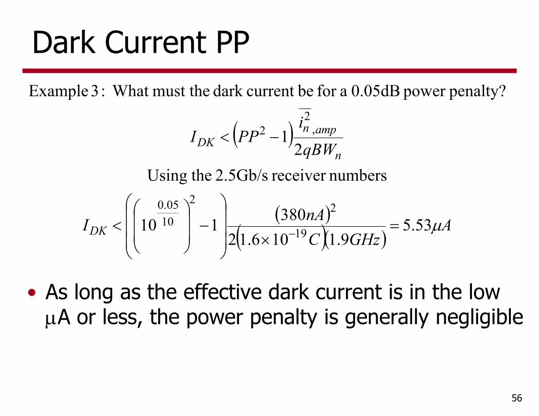
Dark Current PP
AGHzC
nAI
qBWi
PPI
DK
n
ampnDK
53.59.1106.12
380110
numbersreceiver 2.5Gb/s theUsing2
1
penalty?power 0.05dB afor becurrent dark must the What :3 Example
19
22
1005.0
,2
2
• As long as the effective dark current is in the low A or less, the power penalty is generally negligible

Agenda• Receiver Model• Bit-Error Rate• Sensitivity• Personick Integrals• Power Penalties• Bandwidth• Equalization• Jitter• Forward Error Correction
57
Noise vs ISI Bandwidth Trade-Offs• If we design our receiver to have a very wide bandwidth,
then we will receive the signal with minimal distortion
• However, noise will grow as bandwidth increases
• From a basic sensitivity perspective, decreasing bandwidth results in ever-improving sensitivity
• However, this neglects the filtering of the high-frequency pulses (bits) which causes intersymbol interference (ISI)
• Thus, there is an optimum bandwidth from a sensitivity perspective to balance noise and ISI
• This optimum bandwidth is generally about (2/3)B
58
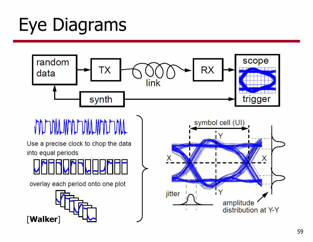
Eye Diagrams
59
[Walker]

Eye Diagrams vs Data Rate
60
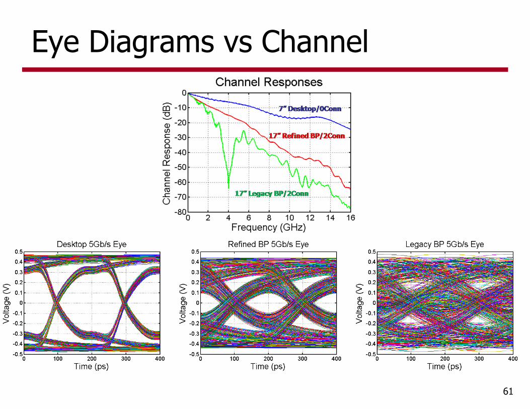
Eye Diagrams vs Channel
61
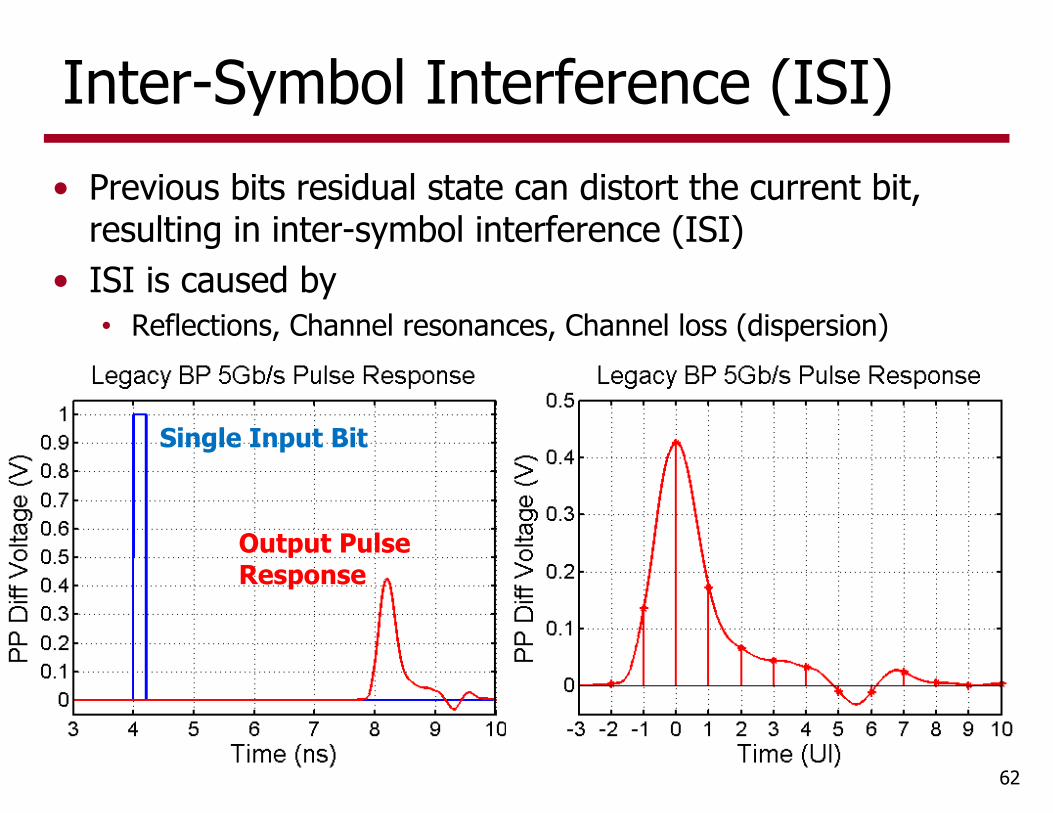
Inter-Symbol Interference (ISI)• Previous bits residual state can distort the current bit,
resulting in inter-symbol interference (ISI)• ISI is caused by
• Reflections, Channel resonances, Channel loss (dispersion)
62
Single Input Bit
Output Pulse Response
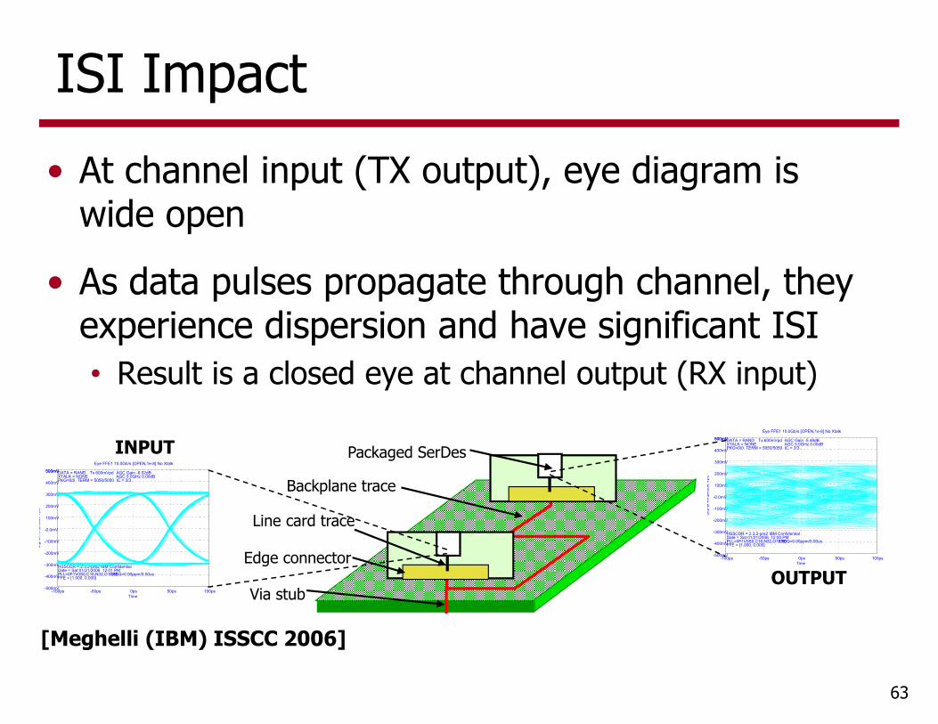
ISI Impact• At channel input (TX output), eye diagram is
wide open
• As data pulses propagate through channel, they experience dispersion and have significant ISI• Result is a closed eye at channel output (RX input)
63
Edge connector
Packaged SerDes
Line card trace
Backplane trace
Via stub
-100ps 100ps-50ps 0ps 50ps-500mV
500mV
-400mV
-300mV
-200mV
-100mV
-0.0mV
100mV
200mV
300mV
400mV
500mV
Eye FFE1 10.0Gb/s [OPEN,1e-8] No Xtalk
Time
Sign
al A
mpl
itude
Vpd
DATA = RAND Tx 600mVpd AGC Gain -5.48dBXTALK = NONE AGC 5.0GHz 0.00dBPKG=0/0 TERM = 5050/5050 IC = 3/3
HSSCDR = 2.3.2-pre2 IBM ConfidentialDate = Sat 01/21/2006 12:00 PMPLL=0F1V0S0,C16,N32,O1,L80 FREQ=0.00ppm/0.00usFFE = [1.000, 0.000]
-100ps 100ps-50ps 0ps 50ps-500mV
500mV
-400mV
-300mV
-200mV
-100mV
-0.0mV
100mV
200mV
300mV
400mV
500mV
Eye FFE1 10.0Gb/s [OPEN,1e-8] No Xtalk
Time
Sign
al A
mpl
itude
Vpd
DATA = RAND Tx 600mVpd AGC Gain -6.02dBXTALK = NONE AGC 5.0GHz 0.00dBPKG=0/0 TERM = 5050/5050 IC = 3/3
HSSCDR = 2.3.2-pre2 IBM ConfidentialDate = Sat 01/21/2006 12:01 PMPLL=0F1V0S0,C16,N32,O1,L80 FREQ=0.00ppm/0.00usFFE = [1.000, 0.000]
INPUT
OUTPUT
[Meghelli (IBM) ISSCC 2006]
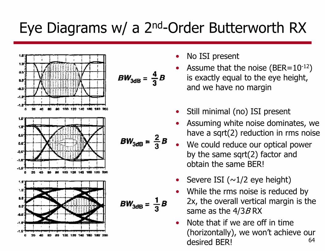
Eye Diagrams w/ a 2nd-Order Butterworth RX
64
• No ISI present• Assume that the noise (BER=10-12)
is exactly equal to the eye height, and we have no margin
• Still minimal (no) ISI present• Assuming white noise dominates, we
have a sqrt(2) reduction in rms noise • We could reduce our optical power
by the same sqrt(2) factor and obtain the same BER!
• Severe ISI (~1/2 eye height)• While the rms noise is reduced by
2x, the overall vertical margin is the same as the 4/3B RX
• Note that if we are off in time (horizontally), we won’t achieve our desired BER!
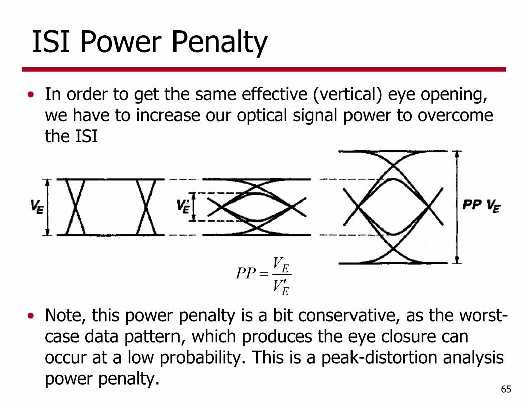
ISI Power Penalty
65
E
EVVPP
• In order to get the same effective (vertical) eye opening, we have to increase our optical signal power to overcome the ISI
• Note, this power penalty is a bit conservative, as the worst-case data pattern, which produces the eye closure can occur at a low probability. This is a peak-distortion analysis power penalty.
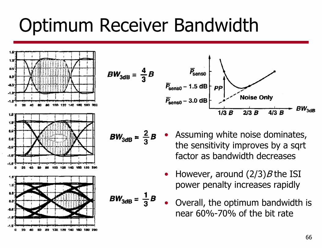
Optimum Receiver Bandwidth
66
• Assuming white noise dominates, the sensitivity improves by a sqrtfactor as bandwidth decreases
• However, around (2/3)B the ISI power penalty increases rapidly
• Overall, the optimum bandwidth is near 60%-70% of the bit rate

Will a B/3 Bandwidth RX Work?
67
• If I am willing to live with a 1.5dB degradation in sensitivity, can I design my receiver with B/3 bandwidth?• 13.3GHz for a 40Gb/s RX!
• Maybe, there is much more sensitivity to timing noise (jitter)• Note that while the (4/3)B
receiver has theoretically the same sensitivity, it maintains the same effective eye height over a much wider time window
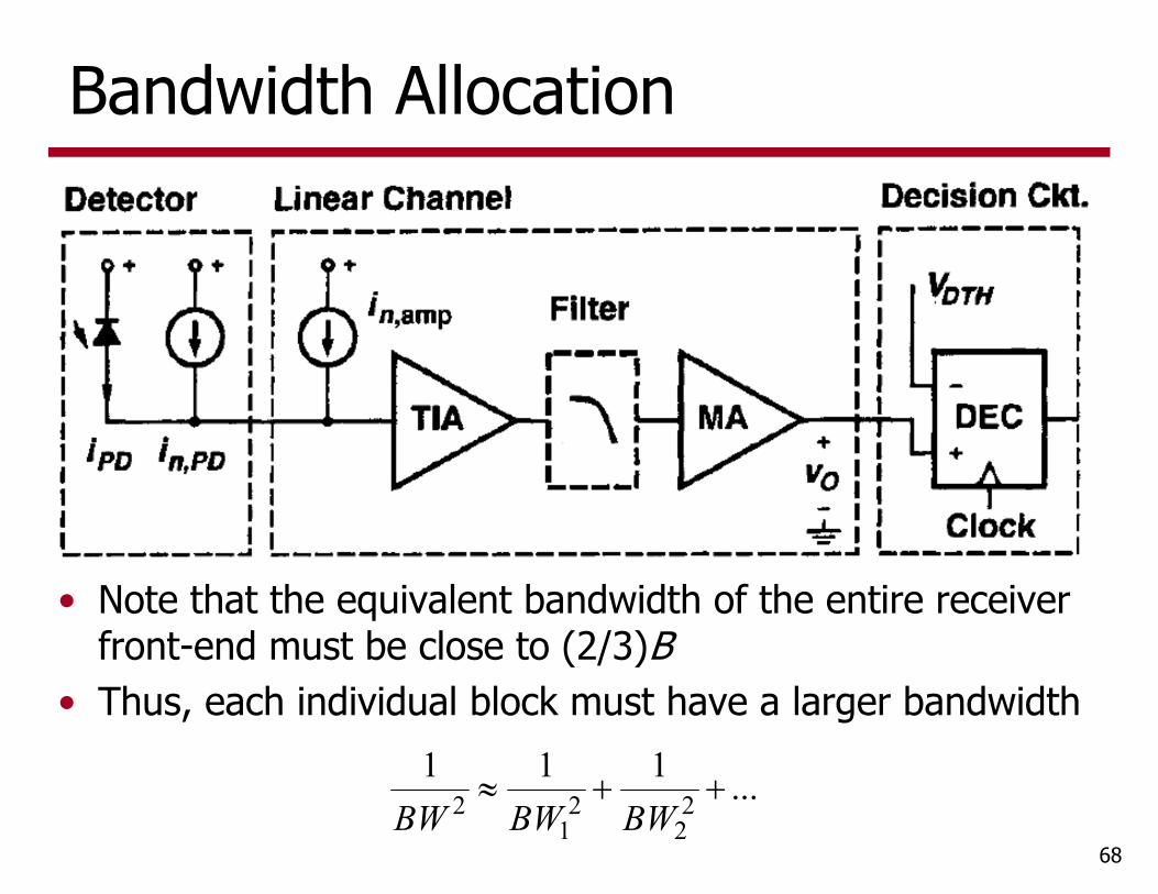
Bandwidth Allocation
68
• Note that the equivalent bandwidth of the entire receiver front-end must be close to (2/3)B
• Thus, each individual block must have a larger bandwidth
...1112
22
12
BWBWBW
Bandwidth Allocation Strategies
69
• Wide bandwidth circuits and a precise low-pass filter• Often a Bessel-Thompson filter is used to limit the noise• Applicable for low-speed receivers (<2.5Gb/s)
• TIA sets the receiver bandwidth• Allows for a higher TIA gain and better noise performance• This means that the subsequent MA stages need to have a much
wider bandwidth• Higher bandwidth than a fixed filter, but also less controlled
• All blocks have similar bandwidths• If we are designing at the highest speeds, then we can’t afford to
overdesign any of the blocks• Applicable for higher-speed receivers (>10Gb/s)
Optimum Receiver Response
70
• While we have shown that a bandwidth of ~(2/3)B is optimum from a receiver-induced ISI and noise perspective, is this truly the optimal response when we consider other factors?
• Important factors• Received signal ISI• Input-referred noise spectrum• RX clock jitter• Bit estimation technique
Low ISI Input Optimal RX Response
71
• A matched filter receiver maximizes the sampled signal-to-noise ratio if the input ISI is minimal
• This has an impulse response h(t) which is proportional to a time-reversed copy of the received pulses x(t)
• For NRZ signals, this is a simple rectangular filter with an impulse response being a rectangular pulse with length of one bit period
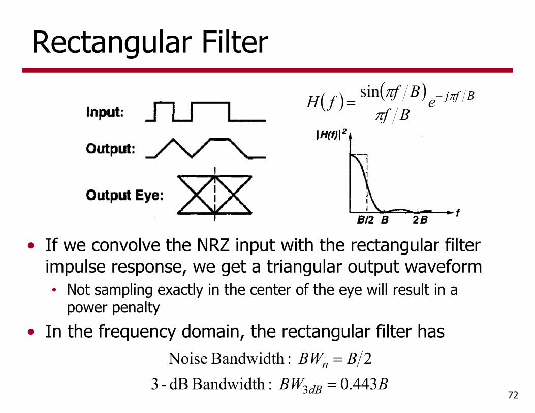
Rectangular Filter
72
• If we convolve the NRZ input with the rectangular filter impulse response, we get a triangular output waveform• Not sampling exactly in the center of the eye will result in a
power penalty• In the frequency domain, the rectangular filter has
BfjeBf
BffH
sin
BBWBBW
dB
n
443.0 :Bandwidth dB-32 :Bandwidth Noise
3
73
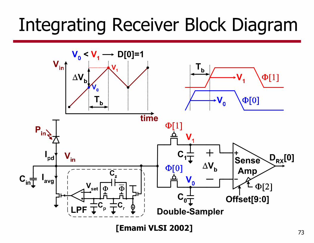
Integrating Receiver Block Diagram
[Emami VLSI 2002]
74
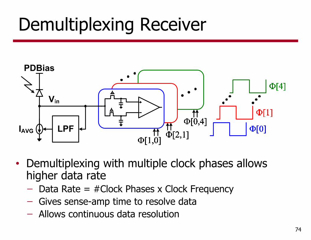
Demultiplexing Receiver
• Demultiplexing with multiple clock phases allows higher data rate̶ Data Rate = #Clock Phases x Clock Frequency̶ Gives sense-amp time to resolve data̶ Allows continuous data resolution
Agenda• Receiver Model• Bit-Error Rate• Sensitivity• Personick Integrals• Power Penalties• Bandwidth• Equalization• Jitter• Forward Error Correction
75
What If We Have Significant ISI?
76
• If we have significant ISI in our system, then an integrating receiver is not optimal
• It is preferred to have a receiver with bandwidth ~(2/3)B to filter the noise, and then have circuitry which cancels the ISI
• A Viterbi decoder, which performs a maximum-likelihood sequence detection, is an optimum realization of an ISI canceller. However, this is generally too complex (power/area).
• Instead, an equalizer is often used to cancel ISI
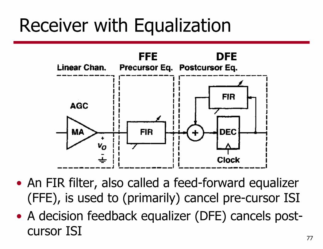
Receiver with Equalization
77
• An FIR filter, also called a feed-forward equalizer (FFE), is used to (primarily) cancel pre-cursor ISI
• A decision feedback equalizer (DFE) cancels post-cursor ISI
FFE DFE
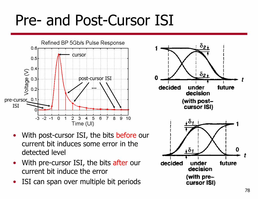
Pre- and Post-Cursor ISI
78
cursor
post-cursor ISI
pre-cursor ISI
…
• With post-cursor ISI, the bits before our current bit induces some error in the detected level
• With pre-cursor ISI, the bits after our current bit induce the error
• ISI can span over multiple bit periods
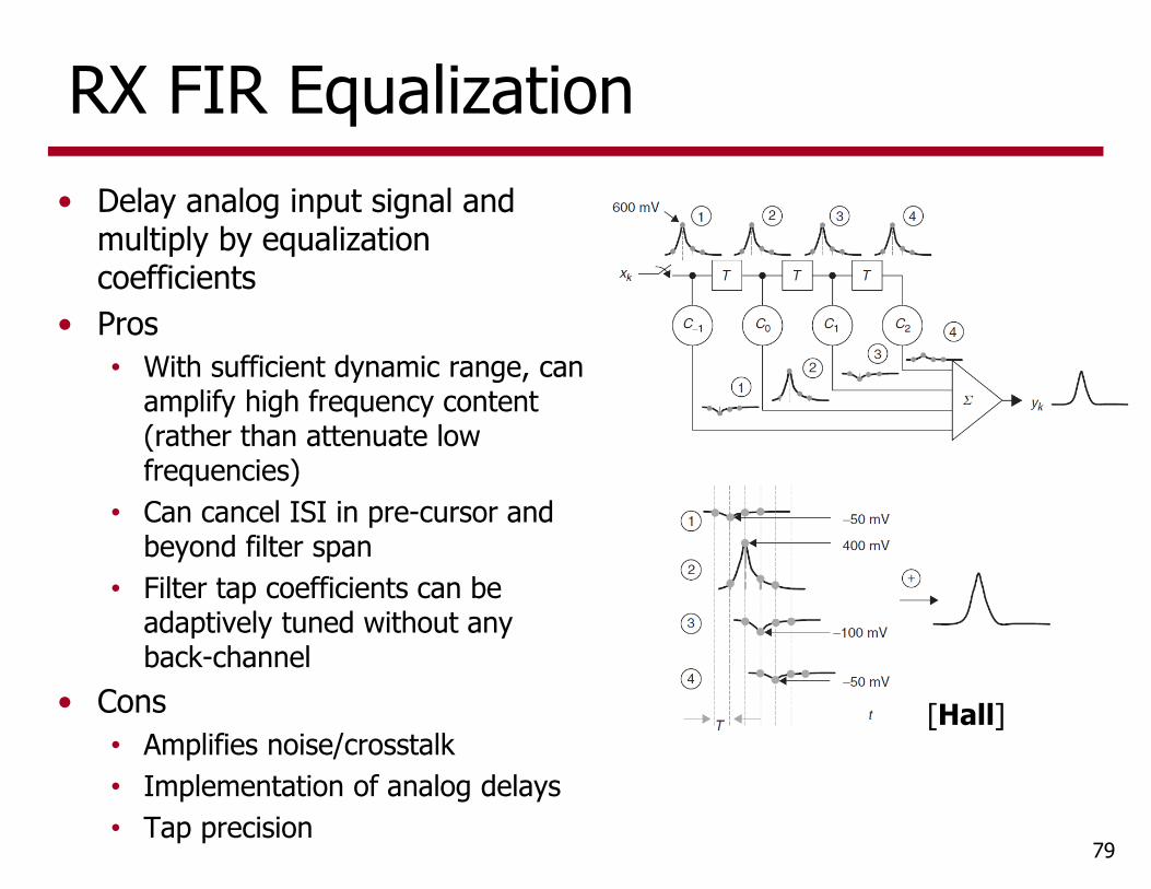
RX FIR Equalization• Delay analog input signal and
multiply by equalization coefficients
• Pros• With sufficient dynamic range, can
amplify high frequency content (rather than attenuate low frequencies)
• Can cancel ISI in pre-cursor and beyond filter span
• Filter tap coefficients can be adaptively tuned without any back-channel
• Cons• Amplifies noise/crosstalk• Implementation of analog delays• Tap precision
79
[Hall]
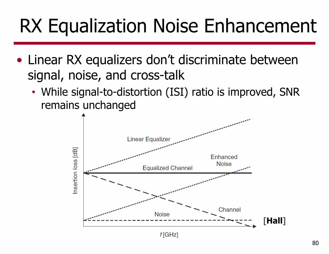
RX Equalization Noise Enhancement• Linear RX equalizers don’t discriminate between
signal, noise, and cross-talk• While signal-to-distortion (ISI) ratio is improved, SNR
remains unchanged
80
[Hall]
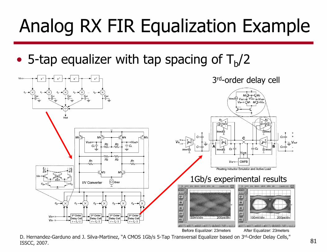
Analog RX FIR Equalization Example
81D. Hernandez-Garduno and J. Silva-Martinez, “A CMOS 1Gb/s 5-Tap Transversal Equalizer based on 3rd-Order Delay Cells," ISSCC, 2007.
• 5-tap equalizer with tap spacing of Tb/2
1Gb/s experimental results
3rd-order delay cell

RX Decision Feedback Equalization (DFE)• DFE is a non-linear
equalizer
• Slicer makes a symbol decision, i.e. quantizes input
• ISI is then directly subtracted from the incoming signal via a feedback FIR filter
82
nknnknkkk dwdwdwyz ~
1
~
11
~
1
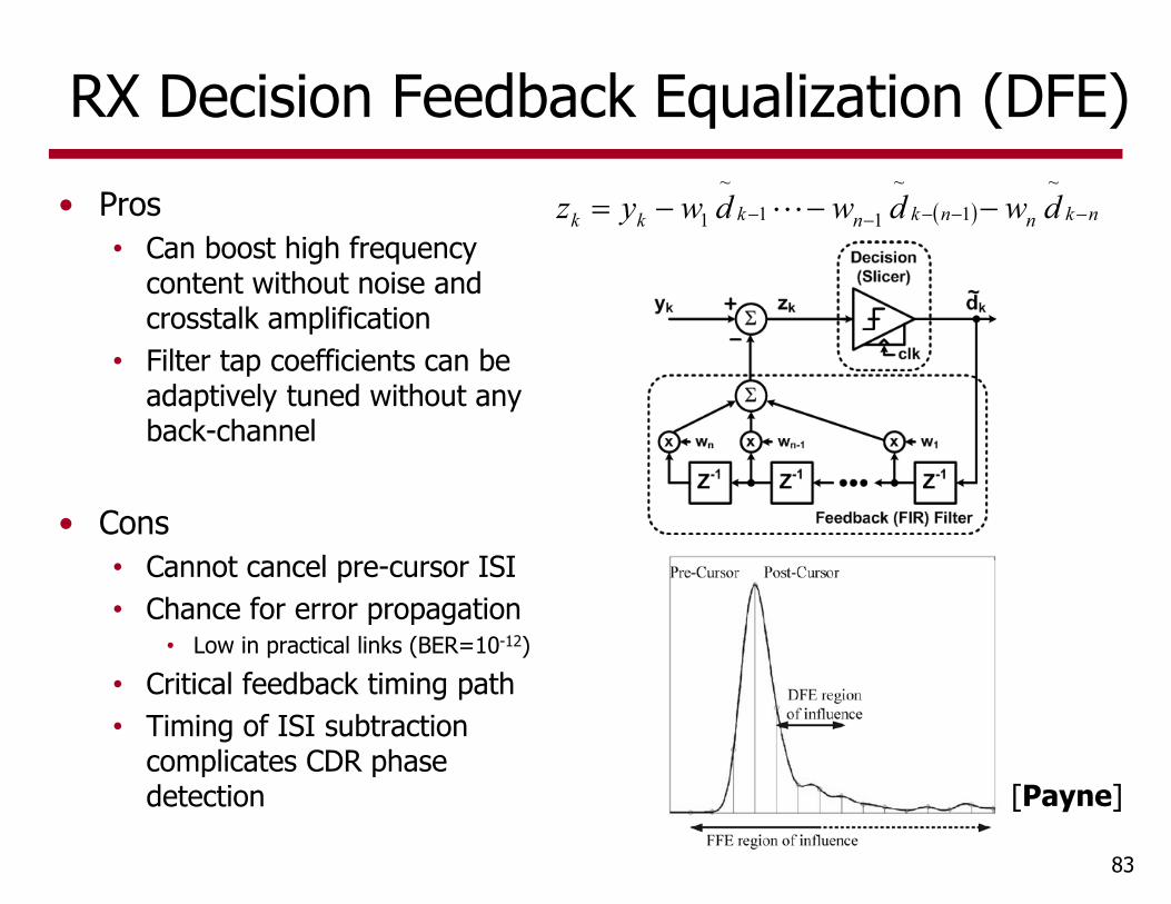
RX Decision Feedback Equalization (DFE)• Pros
• Can boost high frequency content without noise and crosstalk amplification
• Filter tap coefficients can be adaptively tuned without any back-channel
• Cons• Cannot cancel pre-cursor ISI• Chance for error propagation
• Low in practical links (BER=10-12)• Critical feedback timing path• Timing of ISI subtraction
complicates CDR phase detection
83
nknnknkkk dwdwdwyz ~
1
~
11
~
1
[Payne]
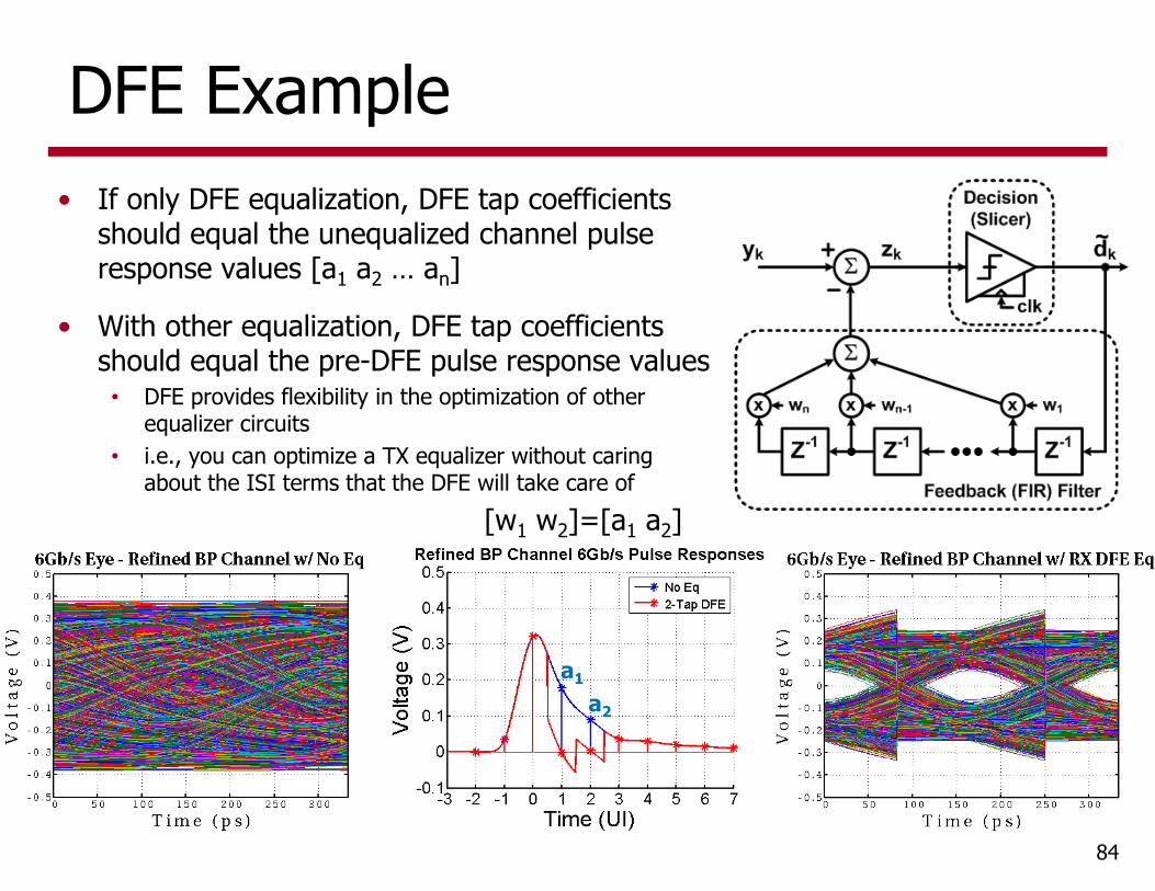
DFE Example
84
• If only DFE equalization, DFE tap coefficients should equal the unequalized channel pulse response values [a1 a2 … an]
• With other equalization, DFE tap coefficients should equal the pre-DFE pulse response values
• DFE provides flexibility in the optimization of other equalizer circuits
• i.e., you can optimize a TX equalizer without caring about the ISI terms that the DFE will take care of
a1
a2
[w1 w2]=[a1 a2]
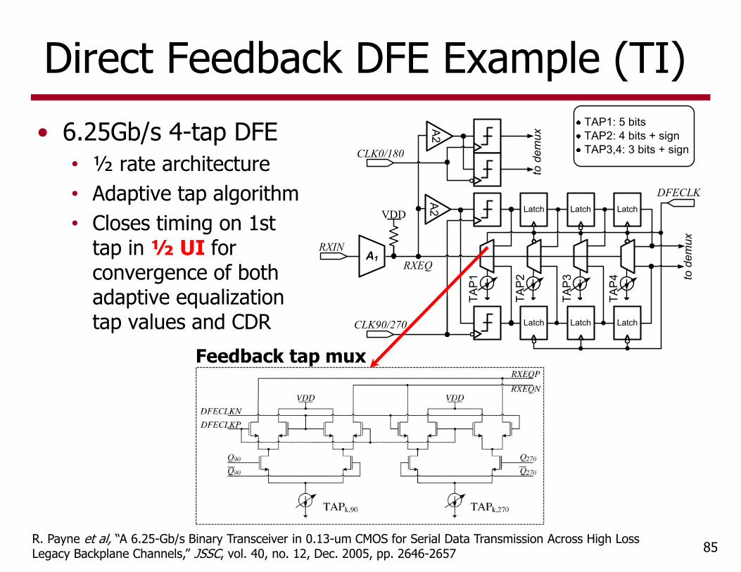
Direct Feedback DFE Example (TI)• 6.25Gb/s 4-tap DFE
• ½ rate architecture• Adaptive tap algorithm• Closes timing on 1st
tap in ½ UI for convergence of both adaptive equalization tap values and CDR
85
TAP1
Latch Latch Latch
TAP2
TAP4
TAP3
Latch Latch Latch
A2A2
VDD
RXEQRXIN
CLK0/180
CLK90/270
DFECLK
to d
emux
to d
emux
A1
TAP1: 5 bitsTAP2: 4 bits + signTAP3,4: 3 bits + sign
Feedback tap mux
R. Payne et al, “A 6.25-Gb/s Binary Transceiver in 0.13-um CMOS for Serial Data Transmission Across High Loss Legacy Backplane Channels,” JSSC, vol. 40, no. 12, Dec. 2005, pp. 2646-2657
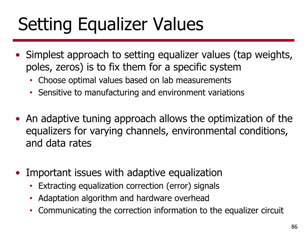
Setting Equalizer Values• Simplest approach to setting equalizer values (tap weights,
poles, zeros) is to fix them for a specific system• Choose optimal values based on lab measurements• Sensitive to manufacturing and environment variations
• An adaptive tuning approach allows the optimization of the equalizers for varying channels, environmental conditions, and data rates
• Important issues with adaptive equalization• Extracting equalization correction (error) signals• Adaptation algorithm and hardware overhead• Communicating the correction information to the equalizer circuit
86
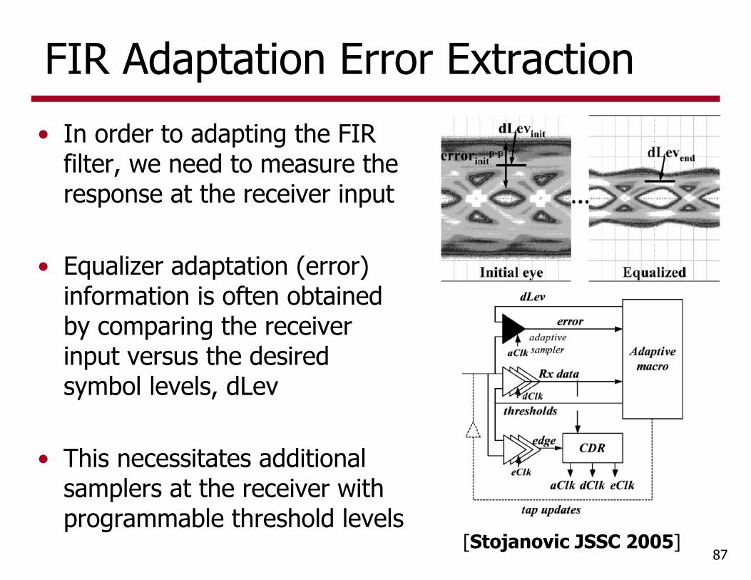
FIR Adaptation Error Extraction• In order to adapting the FIR
filter, we need to measure the response at the receiver input
• Equalizer adaptation (error) information is often obtained by comparing the receiver input versus the desired symbol levels, dLev
• This necessitates additional samplers at the receiver with programmable threshold levels
87[Stojanovic JSSC 2005]
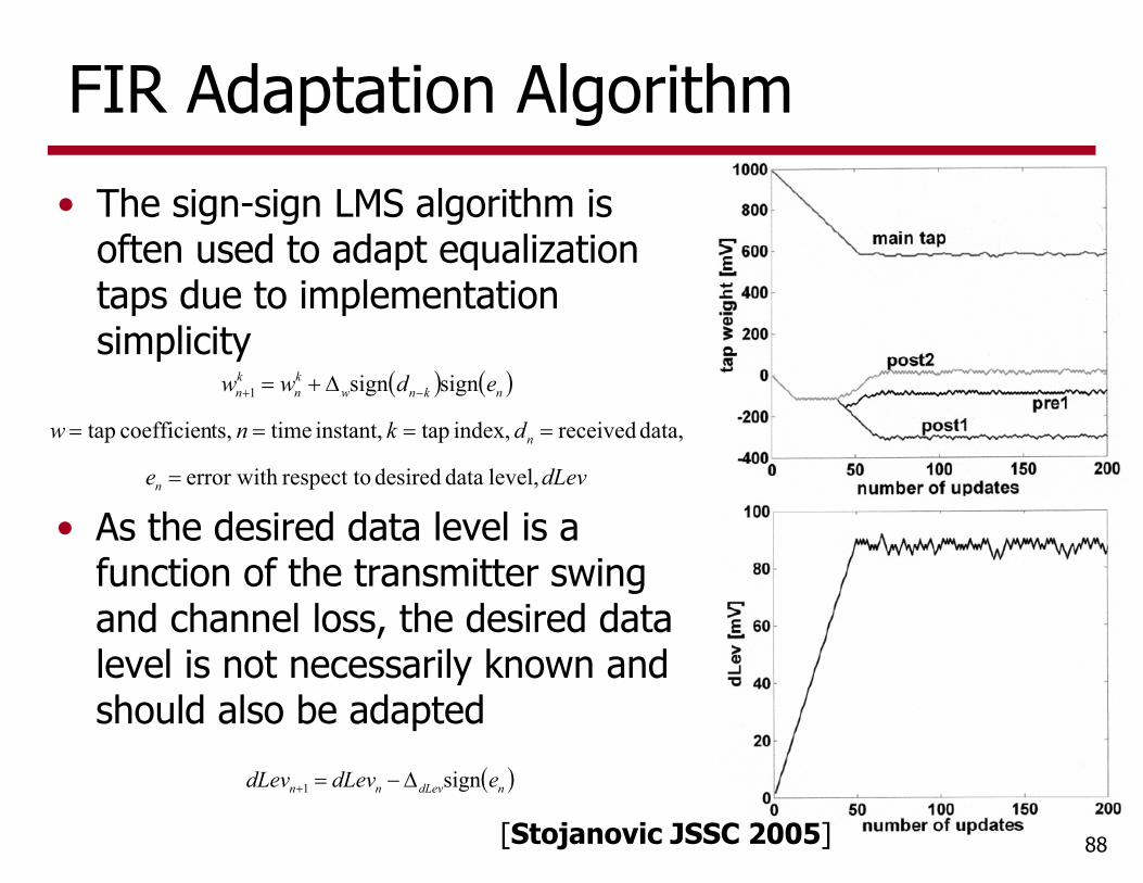
FIR Adaptation Algorithm• The sign-sign LMS algorithm is
often used to adapt equalization taps due to implementation simplicity
88
dLeve
dknw
edww
n
n
nknwkn
kn
level, data desired respect to error with
data, received index, tap instant, time ts,coefficien tap
signsign1
• As the desired data level is a function of the transmitter swing and channel loss, the desired data level is not necessarily known and should also be adapted
ndLevnn edLevdLev sign1
[Stojanovic JSSC 2005]
Agenda• Receiver Model• Bit-Error Rate• Sensitivity• Personick Integrals• Power Penalties• Bandwidth• Equalization• Jitter• Forward Error Correction
89

Eye Diagram and Spec Mask• Links must have margin in both the voltage AND
timing domain for proper operation• For independent design (interoperability) of TX
and RX, a spec eye mask is used
90
Eye at RX sampler
RX clock timing noise or jitter (random noise only here)
[Hall]
Jitter Histogram
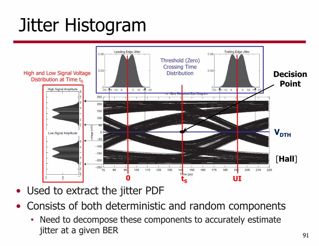
• Used to extract the jitter PDF• Consists of both deterministic and random components
• Need to decompose these components to accurately estimate jitter at a given BER 91
[Hall]
0 UItS
High and Low Signal Voltage Distribution at Time tS
Threshold (Zero) Crossing Time Distribution
VDTH
Decision Point
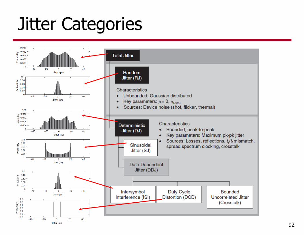
Jitter Categories
92
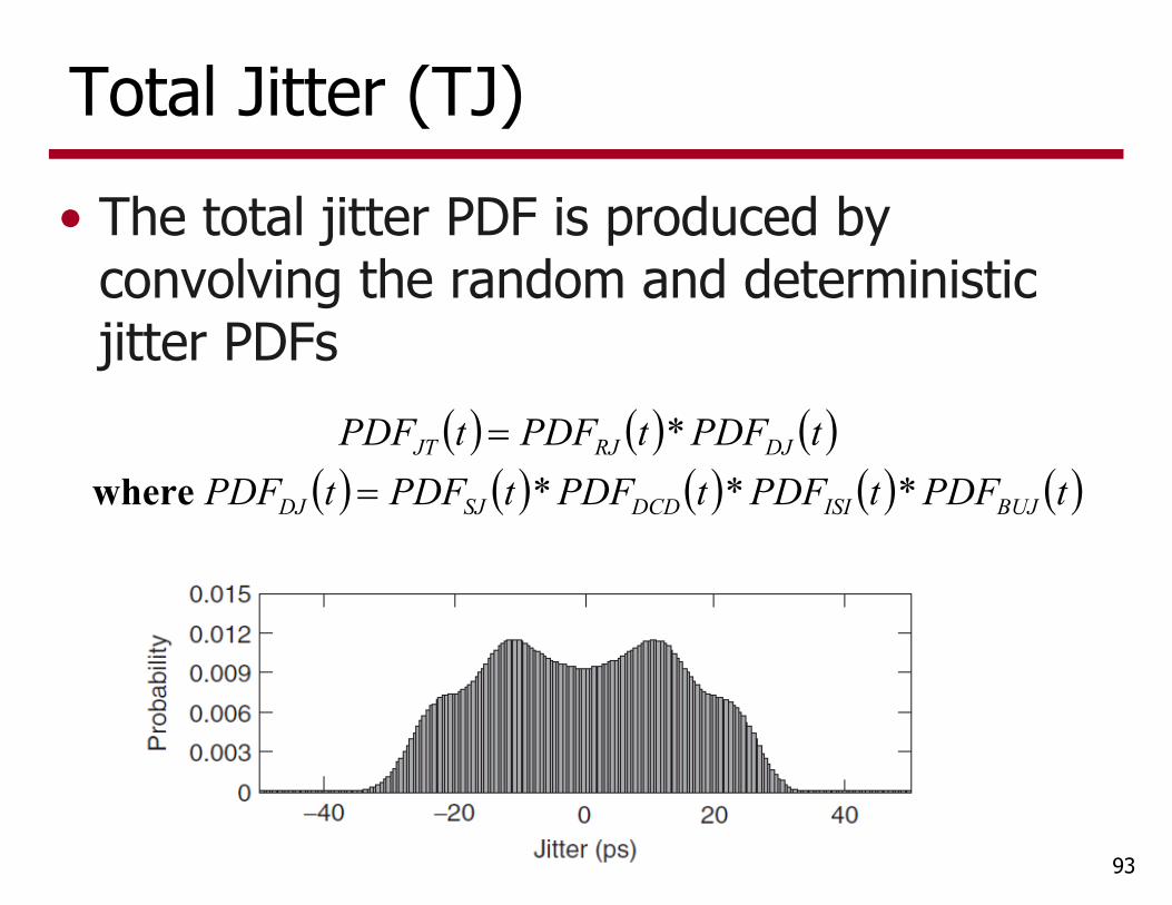
Total Jitter (TJ)• The total jitter PDF is produced by
convolving the random and deterministic jitter PDFs
93
tPDFtPDFtPDFtPDFtPDF
tPDFtPDFtPDF
BUJISIDCDSJDJ
DJRJJT
****
where
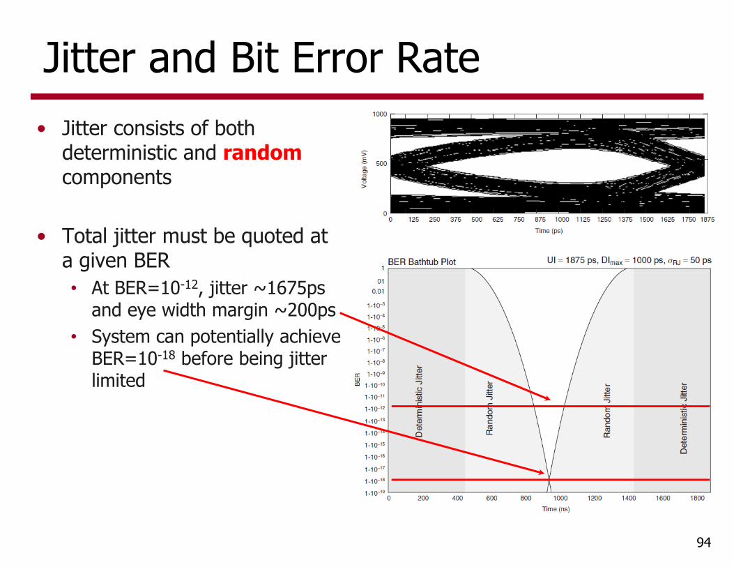
Jitter and Bit Error Rate• Jitter consists of both
deterministic and randomcomponents
• Total jitter must be quoted at a given BER• At BER=10-12, jitter ~1675ps
and eye width margin ~200ps• System can potentially achieve
BER=10-18 before being jitter limited
94
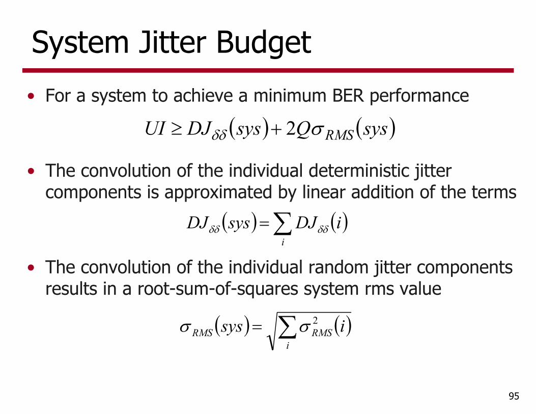
System Jitter Budget• For a system to achieve a minimum BER performance
95
sysQsysDJUI RMS 2
• The convolution of the individual deterministic jitter components is approximated by linear addition of the terms
i
iDJsysDJ
• The convolution of the individual random jitter components results in a root-sum-of-squares system rms value
i
RMSRMS isys 2
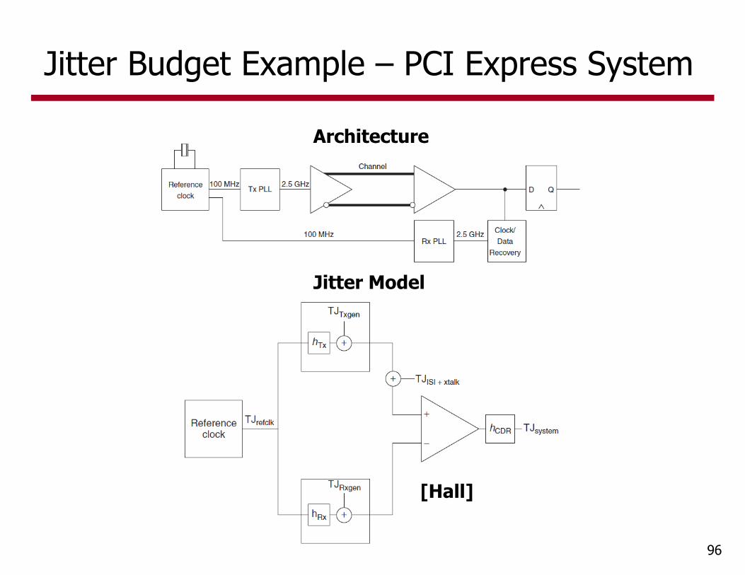
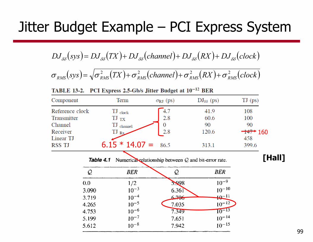
Jitter Budget Example – PCI Express System
96
Architecture
Jitter Model
[Hall]
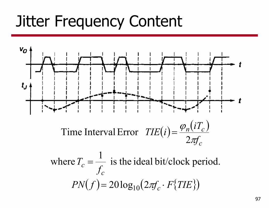
Jitter Frequency Content
97
TIEFffPNf
T
fiTiTIE
c
cc
c
cn
2log20
period.bit/clock ideal theis 1 where
2Error Interval Time
10
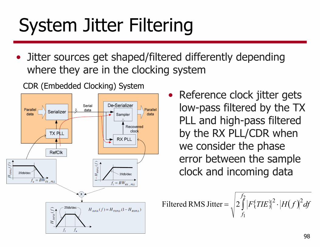
System Jitter Filtering
98
dffHTIEFf
f 2
1
222Jitter RMS Filtered
• Jitter sources get shaped/filtered differently depending where they are in the clocking system
CDR (Embedded Clocking) System• Reference clock jitter gets
low-pass filtered by the TX PLL and high-pass filtered by the RX PLL/CDR when we consider the phase error between the sample clock and incoming data
Jitter Budget Example – PCI Express System
99
clockDJRXDJchannelDJTXDJsysDJ
clockRXchannelTXsys RMSRMSRMSRMSRMS2222
6.15 * 14.07 =[Hall]
160
Agenda• Receiver Model• Bit-Error Rate• Sensitivity• Personick Integrals• Power Penalties• Bandwidth• Equalization• Jitter• Forward Error Correction
100
Forward Error Correction• From previous analysis, we found that we need a
certain SNR for a given BER• w/ NRZ it is Q2 or ~17dB for BER=10-12 (equal noise
statistics)• Can we do better?• Yes, if we add some redundancy in the bits that
we transmit and use this to correct errors at the receiver
• This is called forward error correction (FEC)• Common codes are Reed-Solomon (RS) and Bose-
Chaudhuri-Hocquenghem (BCH)101
Shannon’s Channel Capacity Theorem• If sufficient coding is employed, error-free transmission over
a channel with additive white Gaussian noise is possible for
102
!17dB!an smaller thMuch 08.303.212
thenoverhead) rate data 25% a is(which 0.8r have weif example,For 12
1log2
coding with Thus, rate.bit channel theis and rate code theis where
2
bandwidth channel minimum aneed wesignaling,Nyquist ideal assume weIf coding. with ratebit
channel thelower than is which rate,bit n informatio theis Here1log
8.02
2
2
2
dBSNR
SNR
SNRr
BB
rBr
rBBW
BSNRBWB
r
Reed-Solomon Code Example• Reed-Solomon codes are often used in the
Synchronous Optical Networking (SONET) standard• An important parameter in any error-correcting code
is it’s overhead or redundancy, with a RS(255,239) code having n=255 symbols/codeword, but only k=239 information symbols (although 1 is used for framing and isn’t considered in the data payload)• The overhead is 255/(239-1)=1.071 or 7.1%• This is equivalent to r=238/255=0.933
• A RS(n,k) code can correct for (n-k)/2 symbol errors in a codeword• RS(255,239) can correct for 8 symbols/codeword 103
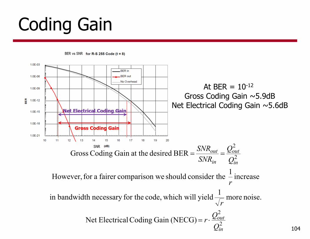
Coding Gain
1042
2
2
2
(NECG)Gain Coding ElectricalNet
noise. more 1 yield l which wilcode, for thenecessary bandwidth in
increase 1heconsider t should wecomparisonfairer afor However,
BER desired at theGain Coding Gross
in
out
in
out
in
out
QQr
r
r
SNRSNR
At BER = 10-12
Gross Coding Gain ~5.9dBNet Electrical Coding Gain ~5.6dB
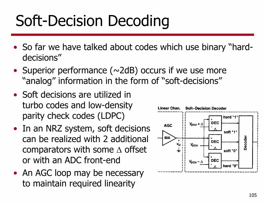
Soft-Decision Decoding• So far we have talked about codes which use binary “hard-
decisions”• Superior performance (~2dB) occurs if we use more
“analog” information in the form of “soft-decisions”
105
• Soft decisions are utilized in turbo codes and low-density parity check codes (LDPC)
• In an NRZ system, soft decisions can be realized with 2 additional comparators with some offset or with an ADC front-end
• An AGC loop may be necessary to maintain required linearity
Next Time• Transimpedance Amplifier (TIA) Circuits
106


