Embed Size (px)
Citation preview

3060 IEEE TRANSACTIONS ON INDUSTRIAL ELECTRONICS, VOL. 57, NO. 9, SEPTEMBER 2010
Dual-Tap Chopping Stabilizer WithSubcyclic AC Soft Switching
Juan Carlos Campo Rodríguez, Member, IEEE, Joaquín Vaquero López, Carlos Cagigal Olay,Santiago Monteso Fernández, Rubén Vela García, and Salvador Martínez García, Senior Member, IEEE
Abstract—AC voltage and phase regulators based on tap chang-ers implemented with silicon-controlled rectifiers and triacs arewidely used due to their robustness. Tap changing is achievedunder natural commutation of semiconductors during the zerocrossing of current, so that the response time exceeds the half cycleof the mains. High-power transistors and gate turn-off thyris-tor switches make new and faster tap commutation techniquespossible to achieve several tap changes in one half cycle. Thispaper analyzes and synthesizes a dual-tap chopping stabilizerwith a compensating transformer, with a pulsewidth-modulationfrequency of about 5 kHz and a new soft-switching techniqueachieved by two auxiliary small-power branches. Unlike othersupercyclic ac soft-switching solutions, the new commutatingmethod allows zero current turn-off, several times in a half cycle,for any sign combination of voltage and current, thus reducing theelectrical stress in the switches and the electromagnetic emission.Zero-crossing current detection is not needed. A technical studyand an evaluation of the power of the required components aredone on the commutation techniques that extend the applicationfield of tap changers to the reduction of the fast perturbationsof the mains as flicker, voltage harmonics, voltage oscillations,etc. Experimental results with insulated-gate bipolar transistorswitches are obtained in a 1 kVA prototype.
Index Terms—AC–AC power conversion, ac chopper, ac voltagestabilizer, on-load tap changer (OLTC), phase regulator.
I. INTRODUCTION
S INCE the worldwide introduction of ac electric trans-mission and distribution systems, electromechanical on-
load tap changers (OLTCs) have been used to solve long-termvoltage variations in low- and medium-power applications. Theappearance of the power semiconductors in the fifties andthe steadily increasing rates and speed since then led to thereplacement of mechanical switches by solid-state counterparts,eliminating the need for frequent and costly maintenance revi-sions and allowing faster operation. Nowadays, most OLTCsfor low-voltage stabilization in the range of 300 VA–300 kVA
Manuscript received July 2, 2008; revised October 18, 2008, December 9,2008, and March 25, 2009; accepted September 15, 2009. Date of publicationDecember 4, 2009; date of current version August 11, 2010. This work wassupported in part by the Spanish Ministry of Science and Technology and inpart by the IBERDROLA Program of Electric Research.
J. C. Campo Rodríguez is with the Department of Electrical and ElectronicEngineering, University of Oviedo, 33204 Gijón, Spain (e-mail: [email protected]).
J. Vaquero López is with the Department of Electronic Technology, Rey JuanCarlos University, 28933 Madrid, Spain (e-mail: [email protected]).
C. Cagigal Olay, S. Monteso Fernández, R. Vela García, andS. Martínez García are with the Departamento de Ingeniería Eléctrica, Elec-trónica y de Control, Universidad Nacional de Educación a Distancia, 28040Madrid, Spain (e-mail: [email protected]; [email protected];[email protected]; [email protected]).
Digital Object Identifier 10.1109/TIE.2009.2037651
230 V single-phase and 400/230 V three-phase stabilizersare based on electronic switches implemented with thyristors(triacs and pairs of unidirectional thyristors in antiparallelorientations) [1]–[3]. Thyristor-based OLTCs are also appliedto phase regulation in long high-voltage electric lines [4], [5].Many efforts are being made to extend the application to replacemechanical switches in multitap transformers for transmissionlines (typically 34.5 kV and 10 MVA in medium voltage)[6], [7]. Thyristor commutation is achieved by eliminating thegate signal of the tap to be disconnected before a natural zerocrossing of the current. Although this soft-switching methodreduces the commutating losses to almost zero, it does not allowmore than one commutation per half cycle (supercyclic commu-tation), so that the response time of the regulator exceeds thisinterval.
Under these circumstances, the appearance of high-powertransistors (bipolar, MOSFET, insulated-gate bipolar transistor(IGBT), etc.) and gate-turn-off thyristor switches (fast GTOs,integrated gate-commutated thryristors, injection-enhancedgate transistors, etc.) allows new and faster tap commutationtechniques, achieving several tap changes in less than a halfcycle (subcyclic commutation) and very low response time[8]–[10]. The new fast tap-changing stabilizers make it possibleto apply OLTCs to the reduction of fast voltage variations suchas steps, distortion, and instability phenomena, as predictedby Musgrave and O’Kelly [11] in the 1970s. They can begrouped into two main topologies: dual-tap chopping stabilizersworking under a permanent pulsewidth-modulation switchingpattern [8], [12], [13] and multitap changers working underdiscrete switching only when a voltage correction is needed[9], [10]. The comparison of the circuits showed in [8]–[10],[13], and [14] with classical OLTCs show that the dual-taptopology suits low-voltage applications in the range of 500 VA–500 kVA, whereas multitap changers can be adapted to bothlow and high voltages, from kilowatts to megawatts. Thesereferences also show that the soft-switching technique used inthis paper allows faster equipment than those obtained by usingzero-crossing current commutation with multitap OLTCs.
In dual-tap chopping solutions, it is important to achievelow commutation losses, since the usual switching patternfrequency is in the range of 1–10 kHz. Solutions using ac quasi-resonant soft switching have been suggested [14] with com-mutation times between 250 and 400 μs typically. The maindisadvantage is the need to detect the exact zero-currentcrossing during the internal commuting oscillations. Buranyproposed a switching strategy using fast unidirectional switchesbased on detecting the polarity of the load current and voltage
0278-0046/$26.00 © 2010 IEEE
CAMPO RODRÍGUEZ et al.: DUAL-TAP CHOPPING STABILIZER WITH SUBCYCLIC AC SOFT SWITCHING 3061
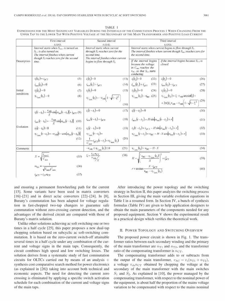
TABLE IEXPRESSIONS FOR THE MOST SIGNIFICANT VARIABLES DURING THE INTERVALS OF THE COMMUTATION PROCESS 1 WHEN CHANGING FROM THE
UPPER TAP TO THE LOWER TAP WITH POSITIVE VOLTAGE AT THE SECONDARY OF THE MAIN TRANSFORMER AND POSITIVE LOAD CURRENT
and ensuring a permanent freewheeling path for the current[15]. Some variants have been used in matrix converters[16]–[21] and in direct ac/ac converters [22]–[24]. In [8],Burany’s commutation has been adapted for voltage regula-tion in fast-chopped two-tap changers to guarantee safecommutation without zero-crossing current detection, and theadvantages of the derived circuit are compared with those ofBurany’s matrix solution.
Unlike other solutions achieving ac soft switching one or twotimes in a half cycle [25], this paper proposes a new dual-tapchopping solution based on subcyclic ac soft-switching com-mutation. It is based on the zero-current switch-off attainableseveral times in a half cycle under any combination of the cur-rent and voltage signs in the main taps. Consequently, thecircuit combines high speed and low switching losses. Thesolution derives from a systematic study of fast commutationcircuits for OLTCs carried out by means of an analysis +synthesis cost comparative search method for power electronics(as explained in [26]) taking into account both technical andeconomic aspects. The need for detecting the current zerocrossing is eliminated by applying a specific switch activationschedule for each combination of the current and voltage signsof the main taps.
After introducing the power topology and the switchingstrategy in Section II, this paper analyzes the switching processin Section III, giving the main variable evolution equations inTable I in a resumed form. In Section IV, a bunch of synthesisformulas (Table IV) are given to help application designers toobtain the main parameters of the components needed for anyproposed equipment. Section V shows the experimental resultin a practical design which verifies the theoretical work.
II. POWER TOPOLOGY AND SWITCHING OVERVIEW
The proposed power circuit is shown in Fig. 1. The trans-former ratios between each secondary winding and the primaryof the main transformer are nT1 and nT2, and the transformerratio of the compensating transformer is nCT.
The compensating transformer adds to or subtracts fromthe output of the main transformer, vAC = vi(nT1 + nT2),a voltage vchnCT obtained by chopping the voltage at thesecondary of the main transformer with the main switchesS1 and S2. As explained in [10], the power managed by thecompensating transformer, with respect to the nominal power ofthe equipment, is about half the proportion of the mains voltagevariation to be compensated with respect to the mains nominal

3062 IEEE TRANSACTIONS ON INDUSTRIAL ELECTRONICS, VOL. 57, NO. 9, SEPTEMBER 2010
Fig. 1. (a) Power circuit topology. (b) Bidirectional switches. (c) Waveform of the chopped voltage at the primary of the compensating transformer. (d) Severalsignificant waveforms.
voltage, which, in a typical application, gives less than 20% ofthe nominal power. Table IV will show 19.12% for the chosennumerical example.
The capacitors Ci1 and Ci2 between taps are used to limitvoltage variations in the secondary of the main transformerdue to the effect of the commutation on its leakage inductance.
Moreover, the capacitors and the primary–secondary leakageinductance of the main transformer act as current filters forthe input current ii, thus reducing the high-frequency currentcomponents injected in the mains.
The switches Saux1 and Saux2 in the auxiliary branch BDare only used during the commutating process between the
CAMPO RODRÍGUEZ et al.: DUAL-TAP CHOPPING STABILIZER WITH SUBCYCLIC AC SOFT SWITCHING 3063
main branches AD and CD so that the commutation in allswitches takes place at zero current. As also explained in [10],the compensating transformer divides typically by 2.5 (1/0.389in the numerical example of Table IV) the load current seenby the main branches. Two different switching processes arepossible, depending on the auxiliary switch (Saux1 or Saux2)turned on to initiate the commutation.
A. Switching Process 1
Saux1 is turned on, and a resonant current begins to circulatebetween the main tap in “ON” state and the auxiliary tap, shapedby Laux1 and Caux. The turning on of Saux1 is at zero currentand forces the current of the conducting main tap to oscillate,making it possible to turn off its switch at zero current. Afterthe initial main tap is disconnected and the current circulatesthrough the auxiliary tap, the main switch of the incoming tapcan be turned on and a similar process begins, so that the mainswitch turns on at zero current through the auxiliary branch andthe auxiliary switch can be turned off at zero current.
In switching process 1, the capacitor should be dischargedprior to a new commutation, this being achieved by resistorRaux.
B. Switching Process 2
Saux2 is turned on, and the current in the main tap in ON
state begins to increase or decrease, depending on the polarityof the voltage at the secondary of the main transformer. If thisincreasing or decreasing current is in the opposite directionto the load current, the main switch can be turned off at zerocurrent. After the initial main tap is disconnected and thecurrent circulates through the auxiliary tap, the main switch ofthe incoming tap can be turned on following a similar process.As the di/dt during the commutation of the switches dependson the value of Laux2, the switches can be turned on at zerocurrent if the inductance value is high enough.
Switching process 2 is only possible when commutating fromthe upper tap to the lower tap and vAC > 0 iLf < 0 or vAC <0 iLf > 0, or when commutating from the lower tap to the uppertap and vAC > 0 iLf > 0 or vAC < 0 iLf < 0. Otherwise, thecurrent in the main tap will not reach zero by turning on theauxiliary switch Saux2. If SW is defined as a variable that ispositive when commutating from the upper tap to the lower tap(S1–S2) and negative when commutating from S2 to S1, then,switching process 2 is only possible when vAC · iLf · SW < 0,for instance, when commutating from the upper tap (branchAD) to the lower tap (branch CD), while vAC > 0 and iLf < 0.
Although switching process 1 could be used under any polar-ity of voltage and current, the time to discharge the capacitormay be too short when the duty cycle is high. However, ifswitching process 1 is only used when vAC · iLf · SW > 0and switching process 2 when vAC · iLf · SW < 0, there is atleast a complete commutation period available to discharge thecapacitor, since a switching process 1 is always followed by aswitching process 2.
Note that, as the commutation itself and the switching strat-egy explained in the next sections cover any combination ofthe signs of the load instantaneous voltage and current, theequipment inherently shall admit any reactive load.
III. ANALYSIS AND SWITCHING SIGNAL TIMING
The circuit analysis will be carried out assuming that thevoltage in the secondary of the main transformer and the loadcurrent do not vary during the switching process because of itsshort duration.
A. Switching Process 1
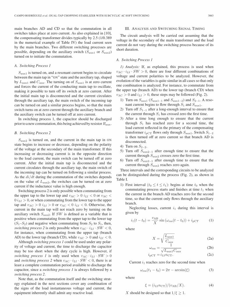
1) Analysis: If, as explained, this process is used whenvAC · iLf · SW > 0, there are four different combinations ofvoltage and current polarities to be analyzed. However, theevolution of the variables is quite similar in all cases so that onlyone combination is analyzed. For instance, to commutate fromthe upper tap (branch AD) to the lower tap (branch CD) whenvAC > 0 and iLf > 0, these steps may be followed (Fig. 2).
1) Turn on Saux1 (Saux1−1 and Saux1−2) and S2−1. A reso-nant current begins to flow through S1 and Saux1.
2) Turn off S1−1 after a long-enough interval to ensure thatthe current through S1 has crossed zero the first time.
3) After a time long enough to ensure that the currentthrough S1 has reached zero for a second time, theload current reflected in the primary of the compensatingtransformer ipCT flows only through Saux1. Switch S1−2
is then turned off at zero current so that branch AD isdisconnected.
4) Turn on S2−2.5) Turn off Saux2−1 after enough time to ensure that the
current through Saux2 crosses zero the first time.6) Turn off Saux2−1 after enough time to ensure that the
current through Saux2 reaches zero again.Three intervals and the corresponding circuits to be analyzed
can be distinguished during the process (Fig. 2), as shown inTable I.
1) First interval (t0 ≤ t ≤ t1): begins at time t0 when thecommutating process starts and finishes at time t1 whenthe current in the branch AD reaches zero for the secondtime, so that the current only flows through the auxiliarybranch.
Neglecting losses, current i1 during this interval isgiven by
i1(t − t0) =vAB
Xsin (ωres(t − t0)) + ipCT (1)
where
X =√
Laux1
Caux(2a)
ωres =1√
Laux1Caux
(2b)
ipCT = iLfnCT. (2c)
Current i1 reaches zero for the second time when
ωres(t1 − t0) = 2π − arcsin(ξ) (3)
where
ξ = (iLfnCT)/(vAB/X). (4)
X should be designed so that 1/ξ ≥ 1.
3064 IEEE TRANSACTIONS ON INDUSTRIAL ELECTRONICS, VOL. 57, NO. 9, SEPTEMBER 2010
Fig. 2. Waveforms during commutation from the upper tap (branch AD) to the lower tap (branch CD) when the voltage at the secondary of the main transformeris positive (vAC > 0) and the load current is positive (iLf > 0).
2) Second interval (t1 ≤ t ≤ t2): begins when the currentin the branch AD reaches zero for the second time andfinishes when the current begins to flow through branchCD. During this interval, all the current iLf/nCT flowsthrough the auxiliary branch, so that the voltage of thecapacitor Caux increases linearly. This interval ends whenvCaux reaches vCD or when S2−2 is closed before that.
3) Third interval (t2 ≤ t ≤ t3): begins when the currentstarts to flow through the lower tap and finishes whenthe current through the auxiliary branch reaches zero forthe second time. The currents in the auxiliary branchand in branch CD evolve in a similar way with the firstinterval.
2) Switching Signal Timing in Process 1: The objective ofthe next analysis is to find a predetermined sequence to turn theswitches on and off so as to make the detection of current zerocrossings unnecessary. Thus, to commutate from the upper tap(branch AD) to the lower tap (branch CD) when vAC > 0 andiLf > 0, the following steps may be followed.
1) At time t0, Saux1 and S2−1 are turned on.2) S1−1 should be turned off between the first and the
second zero crossings of i1. From (9) and (38), time t1,corresponding to the first zero crossing, is
Tres
2≤ t1 − t0 ≤ 3Tres
4, Tres =
2π
ωres. (41)
This means that it is possible to turn off this switch after3/4Tres.
3) S1−2 can be turned off after i1 reaches zero for the secondtime. From (9) and (38), the time t1, corresponding to thissecond zero crossing, is
3Tres
4≤ t1 − t0 ≤ Tres. (42)
This means that it is possible to turn off S1−2 after a timeTres from t0.
4) The switch S2−2 can be turned on a delay time kcTres
after the switch S1−2 is turned off.
Saux1−1 should be turned off after the first zero crossing ofiaux from the beginning of the third interval at time t2, andSaux1−2 should be turned off after the second zero crossing.The time t3, corresponding to the first zero crossing, is givenby (31), and from (29) and (40) and bearing in mind that0 ≤ r ≤ π/2
Tres
4≤ t3 − t2 ≤ Tres
2. (43)
Thus, Saux1−1 can be turned off after Tres/2.Saux1−2 can be turned off after the second zero crossing of
iaux at time t3. From (31),
3Tres
4≤ t3 − t2 ≤ Tres. (44)
Thus, Saux1−2 can be turned off after a time Tres since S2−2
is turned on.If the third interval begins because the voltage in the capac-
itor vCaux reaches the voltage between the auxiliary and the

CAMPO RODRÍGUEZ et al.: DUAL-TAP CHOPPING STABILIZER WITH SUBCYCLIC AC SOFT SWITCHING 3065
Fig. 3. Control signals of the switches where switching process 1 is applicable.
bottom tap vBC, the value of r would be π/2, t3 − t2 =1/4 Tres, and t3 − t2 = 3/4 Tres. To avoid detecting the con-ditions of the beginning of the third interval, the value of kc
should be less than 1/4.Fig. 3 shows the switch control signal timing for every case
where switching process 1 can be applied.The value of kc affects the value of several electrical vari-
ables during the commutation process. Fig. 4(a) shows the valueof the peak current during the third interval with respect to thepeak current in the first interval, for several values of kc. Thepeak current decreases when kc is high; however, the value ofthe voltage across the capacitor at the end of the commutationprocess increases [Fig. 4(b)].
B. Switching Process 2
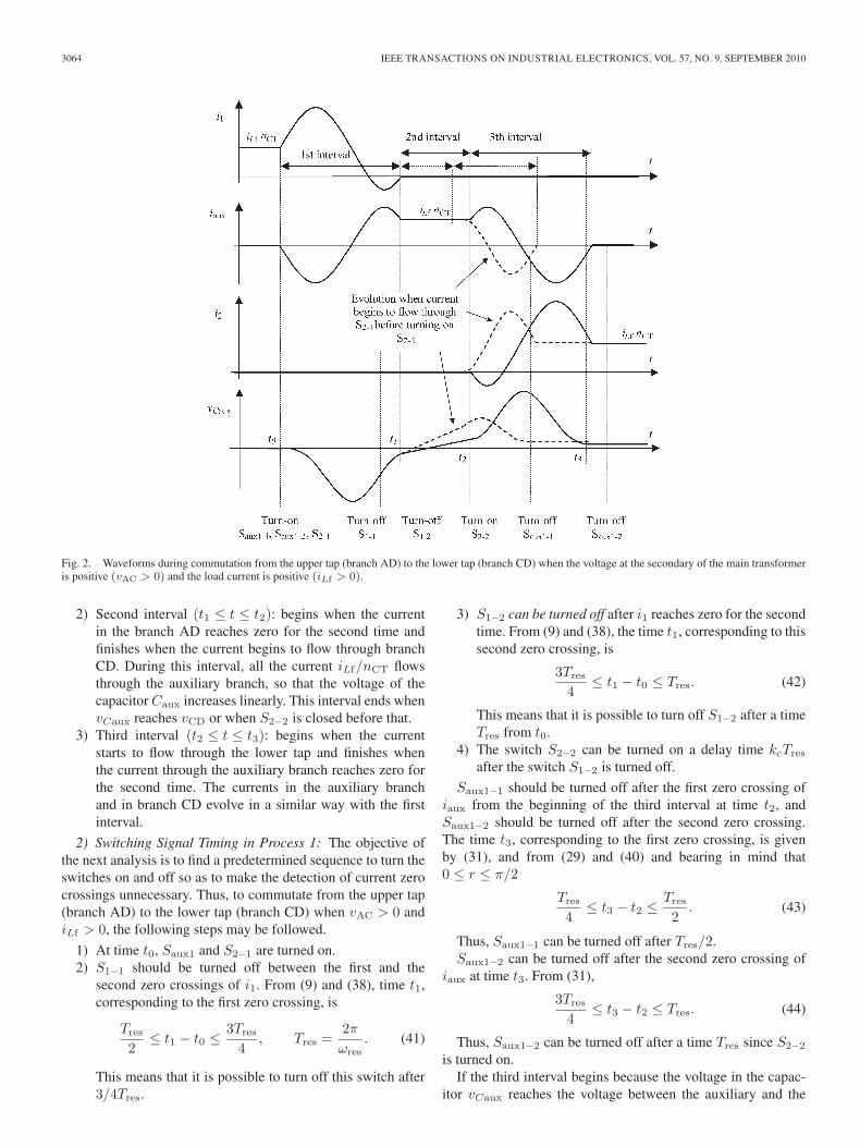
To commutate from the upper tap (branch AD) to the lowertap (branch CD) when vAC > 0 and iLf < 0, the followingsteps may be followed (Fig. 5).
1) Turn off S1−1 at time t0.
2) Turn on Saux2−2 after a short delay time (δt = t1 − t0,1–5 μs) to make sure that S1−1 is turned off. The currentthrough the upper tap decreases linearly while increasingthrough the auxiliary tap.
3) Turn off S1−2 after enough time to ensure that the cur-rent through S1 has reached zero so that the current ofthe primary of the compensating transformer only flowsthrough the auxiliary tap. Assuming that the voltage vAB
between taps and the current ipCT are constant during theswitching process, the time needed for the current in S1
to reach to zero is given by
Δt = t1 − (t0 + δt) =ipCTLaux2
vAB. (45)
4) Turn on S2−2 after a delay time (1–5 μs) to make surethat S1−2 is already off. The current through the auxil-iary tap decreases linearly while increasing through thelower tap.
5) Turn off Saux2−2 after enough time to ensure that thecurrent through Saux2 has reached to zero. Assuming

3066 IEEE TRANSACTIONS ON INDUSTRIAL ELECTRONICS, VOL. 57, NO. 9, SEPTEMBER 2010
Fig. 4. Influence of kc during the commutation process. (a) Value of peakcurrent during the third interval. (b) Voltage across the capacitor at the end ofthe commutation process.
that the voltage vBC between taps and the current ipCT
are constant during the switching process, the time isgiven by
t3 − (t2 + δt) =ipCTLaux2
vBC. (46)
6) S2−1 can be turned on at any time from the beginning ofthe commutation process.
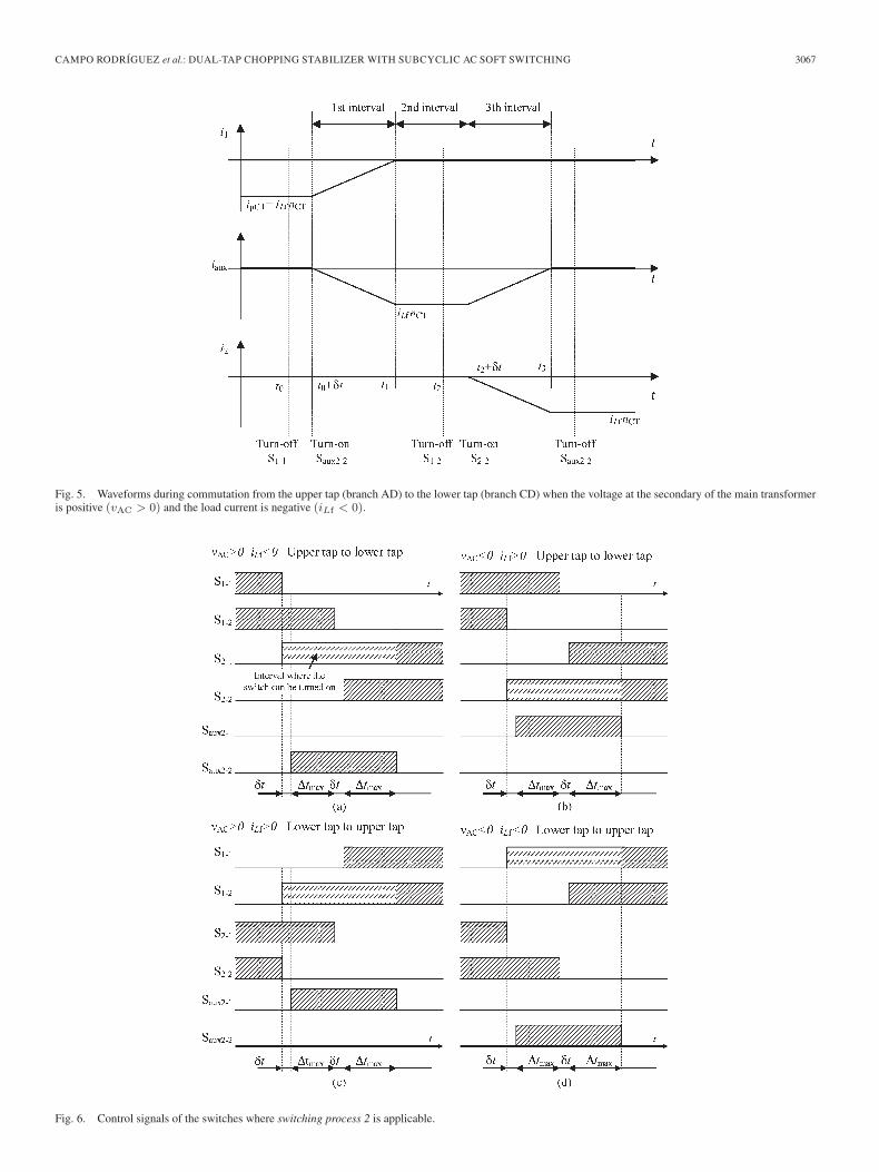
Fig. 6 shows the switch control signal timing for every casewhere switching process 2 is applicable.
IV. SYNTHESIS
A synthesis of the system has been made to obtain the valuesof the electrical rates and working conditions of the componentsas a function of the equipment general specifications (Table II)and auxiliary specifications (Table III). Results for a typical10 kVA stabilizer are included in brackets to compare with [8].
The following assumptions have been made.1) Voltage drops of the main components have been taken
into account to obtain transforming ratios and have beenneglected to obtain voltages and currents in components.
2) Distortions have been neglected in order to obtain volt-ages and currents in components.
3) The values of the components of the filters have beenobtained when duty cycle is 0.5. This is the worst
case condition for the 4 kHz components of the inputcurrent and the output voltage to be filtered. Overloadeffects have been neglected except for the current insemiconductors.
4) Distortion due to inhibition has been neglected.5) The input filter coil has not been considered because it is
normally the leakage inductance of the main transformer.Transformer ratios can be obtained, bearing in mind that the
chopper must add its maximum voltage when the input voltageis at minimum level and must subtract the maximum voltagewhen the input voltage is at maximum level. It is assumed thatthe main transformer supplies nominal output voltage in theintermediate status between the two extreme conditions.
The values of Caux and Laux1 can be obtained under theconditions of ensuring soft-switching using switching process 1and fixing the total time of the commutation process. The firstcondition means that the value of 1/ξ—see (4)—should begreater than one to ensure the zero crossing of the current inthe outgoing branch. Since this value is critical in the designof the system, a more detailed analysis can be done, bearing inmind the quality factor Q of the resonant circuit and the effi-ciency ηCT of the compensating transformer. Thus, (1) is trans-formed into
i1(t − t0) =vAB
Xsin (ωres(t − t0)) e−
ωres(t−t0)2Q + iLf
nCT
ηCT.
(47)
To ensure zero-crossing current, the negative value of thefirst term of the last equation must be equal to or greaterthan the second one. As the maximum negative value of thefirst term happens for t − t0 = 3Tres/4, the condition for softswitching is
vAB/X
iLf (nCT/ηCT)e−
3π4Q ≥ 1. (48)
The value of vAB can be very small depending on the timeof the commutation. Thus, the commutation using process 1should not be allowed when the voltage vAB is small. A goodcriterion is not to allow the commutation when the voltagebetween taps is less than half of the nominal voltage. Thecommutation when the voltage is lower has a small effect on theoutput waveform; moreover, this commutation can be carriedout with low losses using mixed seminatural switching [8] sincethe voltage is small. In this synthesis, we have considered thatthe commutation is not allowed when the voltage in the lowertap is less than half of the nominal voltage VinnT2/2. Thus, thecondition of (48) for ensuring soft switching gets into
VinnT2/2X
iLmaxnCTηCT
e−3π4Q = Ks (49)
where Ks is a security factor. The effects on the output volt-age waveform when inhibiting commutation when the voltagebetween taps is low are studied and quantified in [8].
Moreover, the duration of the commutation is 2Tres + kcTres
(Fig. 3). Thus,
(2 + kc)Tres =dmin
fs. (50)
CAMPO RODRÍGUEZ et al.: DUAL-TAP CHOPPING STABILIZER WITH SUBCYCLIC AC SOFT SWITCHING 3067
Fig. 5. Waveforms during commutation from the upper tap (branch AD) to the lower tap (branch CD) when the voltage at the secondary of the main transformeris positive (vAC > 0) and the load current is negative (iLf < 0).
Fig. 6. Control signals of the switches where switching process 2 is applicable.
3068 IEEE TRANSACTIONS ON INDUSTRIAL ELECTRONICS, VOL. 57, NO. 9, SEPTEMBER 2010
TABLE IIGENERAL SPECIFICATIONS. (VALUES FOR A TYPICAL
SINGLE-PHASE 230 V 50 Hz 10 kVA STABILIZER
ARE INCLUDED IN BRACKETS)
TABLE IIIAUXILIARY SPECIFICATIONS. (VALUES FOR A TYPICAL SINGLE-PHASE
230 V 50 Hz 10 kVA STABILIZER ARE INCLUDED IN BRACKETS)
The values of Laux1 and Caux can be obtained from (49)and (50).
The ohmic value of Raux should be high enough so as notto significantly affect the quality factor of the resonant circuitand low enough so as to discharge the capacitor prior to a newcommutation. There is at least a complete commutation periodavailable to discharge the capacitor, since a switching process 1is always followed by a switching process 2. Assuming that thecapacitor Caux is completely discharged before one third of theswitching period
3RauxCaux ≤ 1fs
. (51)
The value of Laux2 can be obtained, keeping in mind thatswitching process 2 must be completed in less time than thatcorresponding to the minimum duty cycle. As in process 1, ifthe commutation is only allowed when the voltage of the lowertap is greater than half of the nominal voltage and estimatingthe total time to switch from a main tap to the auxiliary one
in 40% of the total commutation time (Fig. 6), the value ofLaux2 is
Laux2 =dmin0.4
fs
VinnT2/2ILmax
nCTηCT
. (52)
The values of the input filter given by Ci1 and Ci2 and thestray inductance of the main transformer can be obtained byfixing the distortion of the voltage of the main transformer andthe input current; the values of the output filter, namely, Lf andCf , can be obtained by fixing the distortion of the stabilizeroutput voltage and the distortion of the current in the filter forthe worst case condition duty cycle of 0.5 [8]. The effect onthe total harmonic distortion of the output voltage is studied in[8]. A more detailed justification of the equations given in thissection is founded in [30]. Resonance between the mains andthe input filter is not likely to happen as the resonant frequencyof the mains series inductance plus input filter ensemble isabout 1 kHz, far from the frequency of the important mainsharmonics of 5◦ (250 Hz) and 7◦ (350 Hz).
Table IV summarizes the synthesis general formula thatgives the parameters and working rates of the components asa function of the general and auxiliary specifications of theequipment. It is a valuable design tool for any practical equip-ment. As an example, given in brackets are the numerical valuesobtained for the 10 kVA example defined, also in brackets, inTables II and III.
Note that although the compensating transformer operatesunder switched voltages of several kilohertz, the voltage andcurrents waves supported have an important 50 Hz componentand small high-frequency components that, in practice, do notraise the losses in both transformers, over a normal 50 Hzdesign, by more than 5% typically.
Conduction losses are given by the sum of the products ofthe voltage and average current.
Table IV makes clear than the proposed stabilizer haseconomical ratings for the main transformer (127% nominalpower) and for the compensating transformer (19% nominalpower) and very small auxiliary components. The main IGBTaverage current is small (11 A for a 10 kVA equipment). Anextra current overrating of the practical main switches of 25%with respect to non-soft-switching solutions is recommendeddue to the very short commutating current peaks.
V. EXPERIMENTAL RESULTS
A single-phase 1 kVA 230 V 50 Hz stabilizer intended tocorrect mains voltage variations in the +10%–15% range hasbeen calculated using the synthesis in Table IV and testedunder open-chain control condition with prefixed duty cycle.The main component rates and results are shown in Table V.
The switching frequency used (5 kHz) is slightly greater thanthat in the 10 kVA numerical example of Table IV (4 kHz) dueto the smaller power. As the power of the prototype, adapted tothe available test facilities, is lower than the power of a typicalapplication (5–50 kVA) and, moreover, small magnetic compo-nents show bigger coil losses than their big power counterparts,a special low-coil-loss design in transformers and inductors has

CAMPO RODRÍGUEZ et al.: DUAL-TAP CHOPPING STABILIZER WITH SUBCYCLIC AC SOFT SWITCHING 3069
TABLE IVPARAMETERS AND WORKING RATES OF THE COMPONENTS—(SOME EXPRESSIONS ARE DELIBERATELY NOT
SIMPLIFIED TO HELP TRACE THE ORIGIN). (VALUES RESULTING FROM THE TYPICAL SINGLE-PHASE
230 V 50 Hz 10 kVA STABILIZER DEFINED IN TABLES II AND III ARE INCLUDED IN BRACKETS)
3070 IEEE TRANSACTIONS ON INDUSTRIAL ELECTRONICS, VOL. 57, NO. 9, SEPTEMBER 2010
TABLE VMAIN VALUES OF THE 1 kVA PROTOTYPE
Fig. 7. Photograph of the 1 kVA prototype showing the main components.
been adopted for the 1 kVA prototype in order to make resultsmore accurately extensive to higher power equipment. Fig. 7shows a photograph of the prototype.
A digital signal processor ADSP-2181 was used to controlthe system. Hall effect sensors were used to measure the po-larity of current (LEM LA25-NP) and voltage (LEM LV-25P).The IGBTs were driven at +15/−5 V using IR2111 drivers; thegate signals were isolated from the control circuit using fiberoptics (HFBR-1414T transmitters and HFBR2114R receivers).
As discussed in the synthesis, soft switching was only usedwhen the instantaneous voltage of the lower tap was higher thanhalf the nominal peak voltage. Seminatural mixed switchingwas used in other situations to avoid distortion of the outputvoltage [8]. Seminatural not-mixed switching produces highdistortion [8] because it is difficult to detect current or voltagepolarities when they are near zero [27]–[29].
To fix the control signals of the switches for switchingprocess 1 (Fig. 3), the experimental resonant period of theresonant auxiliary circuit Laux1, Caux was measured, obtaininga value Tres = 8.5 μs. The value assigned to kc was 0.1.
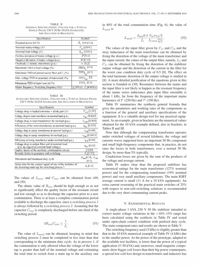
Fig. 8. Main waveforms and control signals of the switches during commu-tation from the upper tap to the lower tap when the voltage at the secondaryof the main transformer is positive (vAC > 0) and the load current is positive(iLf > 0) using switching process 1 (vAC = 300 V, duty cycle d = 0.5, andnominal resistive load).
Fig. 8 shows the waveforms of the current of each tap duringthe commutation from the upper tap to the lower tap whencurrent and voltage are positive and the voltage of the auxiliarycapacitor VCaux using the control signals of the switches shownin Fig. 3. This figure was obtained for nominal input voltagewhen the instantaneous voltage between taps and the currentare high, using a resistive load, so that peak current is near themaximum value.
Fig. 8 shows that the peak current of i1 (12.5 A) is muchhigher than necessary to ensure that, when the voltage is low,the peak current will be high enough to force a zero crossing.When commutating at half the peak mains voltage, that peakcurrent would be 6.25 A, about 10% greater than the peaknominal load current at the maximum value of input voltage(1 kVA/230 V) ·
√2 = 5.76 A. As the oscillating current lasts
a few microseconds, it does not have practical implications onconductor section.
The waveforms are quite similar to the theoretical predictions(Fig. 2 and Table I), and the commutation of the switches at thecalculated times does not interrupt the current during the tapchange as predicted.
Fig. 9 shows the current and voltage waveforms during atap change showing soft-switching commutations because theturning-on or the turning-off of each switch takes place at zerocurrent and the voltage is near zero when the current begins tocirculate through the switch. The commutations where testedunder every condition where switching process 1 is applicable,showing similar results.
CAMPO RODRÍGUEZ et al.: DUAL-TAP CHOPPING STABILIZER WITH SUBCYCLIC AC SOFT SWITCHING 3071
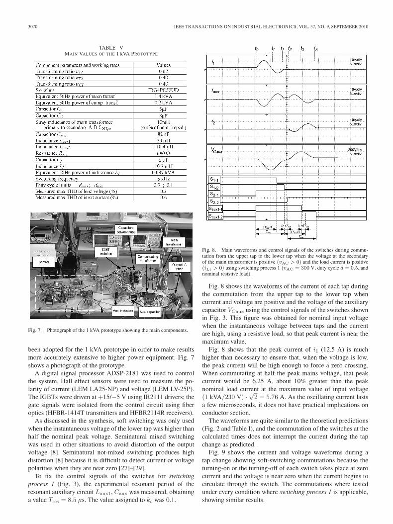
Fig. 9. Current and voltage waveforms in the switches during commutationfrom the upper tap to the lower tap when the voltage at the secondary ofthe main transformer is positive (vAC > 0) and the load current is positive(iLf > 0) using switching process 1 (vAC = 250 V, duty cycle d = 0.5, andnominal resistive load).
Fig. 10. Auxiliary-tap current during the commutation from the lower tap tothe upper tap using switching process 1. The lower trace shows the waveformwith 1 kΩ resistor in parallel with Laux2, and the upper trace shows thewaveform without the resistor.
The gate signal of the switches for switching process 2 whereobtained by fixing δt = 1.2 μs and δt = 6 μs (Fig. 6). InFig. 10, the upper trace shows the current in the auxiliary tapduring the commutation process. High-frequency oscillationsappear during the second and third intervals (about 500 and650 kHz, respectively, in Fig. 10) mainly due to the parasiticcapacitors of the switches. The oscillations during the secondinterval are due to the voltage changes in the switches ofthe upper and lower taps at the end of the first interval. Theoscillations during the third interval are due to the voltagechanges in the switches of the auxiliary tap at the end of thesecond interval.
The oscillations have been reduced by using damping resis-tors: a 1 kΩ 1/4 W resistors in parallel with Laux2 [Fig. 10(lower trace)]. The oscillations were also present in switchingprocess 1. However, in this latter process, the oscillations areless significant because Laux2 < Laux1, the frequency is higherthan that in process 2, and they are easily attenuated. They were
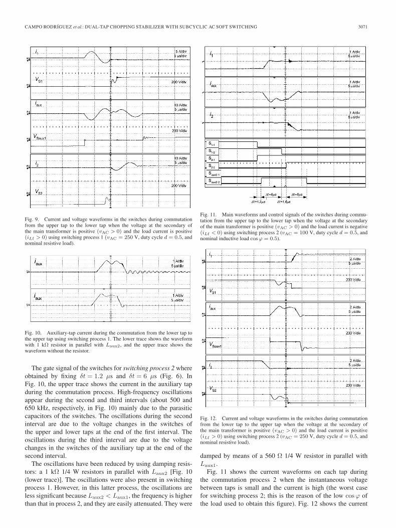
Fig. 11. Main waveforms and control signals of the switches during commu-tation from the upper tap to the lower tap when the voltage at the secondaryof the main transformer is positive (vAC > 0) and the load current is negative(iLf < 0) using switching process 2 (vAC = 100 V, duty cycle d = 0.5, andnominal inductive load cos ϕ = 0.5).
Fig. 12. Current and voltage waveforms in the switches during commutationfrom the lower tap to the upper tap when the voltage at the secondary ofthe main transformer is positive (vAC > 0) and the load current is positive(iLf > 0) using switching process 2 (vAC = 250 V, duty cycle d = 0.5, andnominal resistive load).
damped by means of a 560 Ω 1/4 W resistor in parallel withLaux1.
Fig. 11 shows the current waveforms on each tap duringthe commutation process 2 when the instantaneous voltagebetween taps is small and the current is high (the worst casefor switching process 2; this is the reason of the low cos ϕ ofthe load used to obtain this figure). Fig. 12 shows the current
3072 IEEE TRANSACTIONS ON INDUSTRIAL ELECTRONICS, VOL. 57, NO. 9, SEPTEMBER 2010
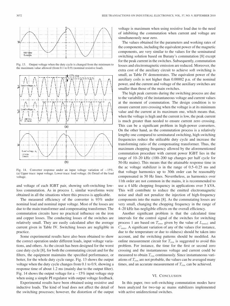
Fig. 13. Output voltage when the duty cycle is changed from the minimum tothe maximum value allowed (from 0.1 to 0.9) (nominal resistive load).
Fig. 14. Converter response under an input voltage variation of −15%.(a) Upper trace: input voltage. Lower trace: load voltage. (b) Detail of the loadvoltage.
and voltage of each IGBT pair, showing soft-switching low-loss commutation. As in process 1, similar waveforms wereobtained in all the situations where this process is applicable.
The measured efficiency of the converter is 93% undernominal load and nominal input voltage. Most of the losses aredue to the main transformer and compensating transformer. Thecommutation circuits have no practical influence on the ironand copper losses. The conducting losses of the switches arerelatively small. They are easily calculated after the averagecurrent given in Table IV. Switching losses are negligible inpractice.
Some experimental results have also been obtained to showthe correct operation under different loads, input voltage varia-tions, and others. As the circuit has been designed for the worstcase duty cycle [8], for both the commutating circuit and for thefilters, the equipment maintains the specified performance, orbetter, for the whole duty cycle range. Fig. 13 shows the outputvoltage when the duty cycle changes from 0.1 to 0.9, showing aresponse time of about 1.2 ms (mainly due to the output filter).Fig. 14 shows the output voltage for a −15% input voltage stepwhen using a simple PI regulator with output voltage feedback.
Experimental results have been obtained using resistive andinductive loads. The kind of load does not affect the detail ofthe switching processes; however, the distortion of the output
voltage is maximum when using resistive load due to the needof inhibiting the commutation when current and voltage aresimultaneously near zero.
The values obtained for the parameters and working rates ofthe components, including the equivalent power of the magneticcomponents, are very similar to the values for the seminaturalswitching solution based on Burany’s commutation [8] exceptfor the peak current in the switches. Subsequently, commutationlosses and electromagnetic emission are reduced. Moreover, theextra cost of the auxiliary circuit to achieve soft switching issmall, as Table IV demonstrates. The equivalent power of theauxiliary coils is not higher than 0.00002 p.u. of the nominalpower, and the current and voltage of the auxiliary switches aresmaller than those of the main switches.
The high peak currents during the switching process are dueto the variability of the instantaneous voltage and current valuesat the moment of commutation. The design condition is toensure current zero crossing when the voltage is at its minimumvalue and the current at its maximum one, which means that,when the voltage is high and the current is low, the peak currentis much greater than needed to ensure current zero crossing.This can be a significant problem in high-power converters.On the other hand, as the commutation process is a relativelylengthy one compared to seminatural switching, high switchingfrequencies reduce the utilizable duty cycle and increase thetransforming ratio of the compensating transformer. Thus, themaximum chopping frequency allowed by the aforementionedcommutation procedure with current power IGBT lies in therange of 10–20 kHz (100–200 tap changes per half cycle for50-Hz mains). This means that the attainable response time inthe ac voltage stabilizer is in the range of 0.5–0.25 ms andthat voltage harmonics up to 30th order can be reasonablycompensated in 50 Hz lines. Nevertheless, as harmonics over11th order are not common in the mains, it is recommended touse a 4 kHz chopping frequency in applications over 5 kVA.This will contribute to reduce the emitted electromagneticnoise and shall not penalize the injection of high-frequencycomponents into the mains [8]. As the commutating losses arevery small, changing the chopping frequency in the range of4–20 kHz has negligible effects on the overall efficiency.
Another significant problem is that the calculated timeintervals for the control signal of the switches for switchingprocess 1 are based on Tres, given by the value of Laux1 andCaux. A significant variation of any of the values (for instance,due to the temperature or due to oldness) should be taken intoaccount, and the switching patterns should be modified. Anonline measurement circuit for Tres is suggested to avoid thisproblem. For instance, the time for the first or second zerocrossing and the instantaneous voltage and current could bemeasured to obtain Tres continuously. Since instantaneous vari-ations of Tres are not probable, the values can be averaged manytimes, and an accurate measurement of Tres can be achieved.
VI. CONCLUSION
In this paper, two soft-switching commutation modes havebeen analyzed for two-tap ac mains stabilizers implementedwith active unidirectional switches.
CAMPO RODRÍGUEZ et al.: DUAL-TAP CHOPPING STABILIZER WITH SUBCYCLIC AC SOFT SWITCHING 3073
In both processes, the switches are turned on at zero current,owing to an auxiliary circuit that limits the di/dt during thecommutation. Switches are turned off naturally by applying aspecific switch activation schedule for each combination of thecurrent and voltage signs of the main taps. It is not necessary todetect the moments of the current zero crossings which wouldbe much more difficult than detecting the current and voltagesigns of the main taps at the beginning of the commutationprocess.
The predicted waves by analysis show good agreement withthe experimental results in a low-power prototype. The onlydeviations are due to the parasitic capacitances of the switchesand have been easily suppressed by adding low-power resistors.
In conclusion, the commutation proposed can be appliedin dual-tap ac voltage chopping stabilizers for the reduc-tion of voltage changes and harmonics in the range of 0.1–100 kVA. The attainable reduction of high-order harmonics byusing high switching frequencies is easier than using seminat-ural switching.
An interesting research line to reduce the high peak currentscould be to add a variable voltage source in the auxiliary tap sothat the resulting voltage of the auxiliary commutation circuitwould be approximately constant under any condition.
REFERENCES
[1] J. Arrillaga, “A static alternative to the transformer on-load tap-changer,” IEEE Trans. Power App. Syst., vol. PAS-99, no. 1, pp. 86–91,Jan. 1980.
[2] E. C. Servetas and V. Vlachakis, “A new AC voltage regulator usingthyristors,” IEEE Trans. Ind. Electron. Control Instrum., vol. 28, no. 2,pp. 140–145, May 1981.
[3] D. Gahigiro, M. A. Erro, and S. Martinez, “AC tap changing stabilizerswith limited commutating current,” in Proc. 1st Power Electron. Int.Congr. IEEE-CENIDET , Cuernavaca, México, Aug. 1992, pp. 195–208.
[4] R. M. Mathur and R. S. Basati, “A thyristor controlled static phase-shifterfor AC power transmission,” IEEE Trans. Power App. Syst., vol. PAS-100,no. 5, pp. 2650–2655, May 1981.
[5] R. Irvani and D. Maratukulam, “Review of semiconductor-controlled (sta-tic) phase shifter for power systems application,” IEEE Trans. Power Syst.,vol. 9, no. 4, pp. 1833–1839, Nov. 1994.
[6] G. Güth, G. R. Baker, and P. Eglin, “Static thyristor-controlled regulat-ing transformer for AC transmission,” in Proc. IEE Int. Conf. Thyris-tor Variable Static Equipment AC, DC Transmission, London, U.K.,Nov./Dec. 1981, pp. 862–869.
[7] P. Wood, V. Bapat, and R. P. Putkovich, “Study of improved load-tap-changing for transformers and phase-angle regulators,” EPRI, Palo Alto,CA, p. 148, Nov. 1988.
[8] J. C. Campo, J. Vaquero, M. A. Perez, and S. Martinez, “Dual-tapchopping stabilizer with mixed seminatural switching. Analysis andsynthesis,” IEEE Trans. Power Del., vol. 20, no. 3, pp. 2315–2326,Jul. 2005.
[9] J. Vaquero, J. C. Campo, S. Monteso, S. Martinez, and M. A. Perez,“Analysis of fast onload multitap-changing clamped-hard-switching ACstabilizers,” IEEE Trans. Power Del., vol. 21, no. 2, pp. 852–861,Apr. 2006.
[10] J. Vaquero, J. C. Campo, S. Monteso, S. Martinez, and M. A. Perez,“Synthesis of fast onload multitap-changing clamped-hard-switching ACstabilizers,” IEEE Trans. Power Del., vol. 21, no. 2, pp. 862–872,Apr. 2006.
[11] G. Musgrave and D. O´Kelly, “Improvement for power system transmis-sion by solid-state techniques,” in Proc. IEE Conf. Power Electron., PowerSemicond., Appl., Dec. 1974, pp. 228–233.
[12] D.-H. Jan and G.-H. Choe, “Step-up/down AC voltage regulator usingtransformer with tap changer and PWM AC chopper,” IEEE Trans. Ind.Electron., vol. 45, no. 6, pp. 905–911, Dec. 1998.
[13] S. Martinez, “Perfeccionamientos introducidos en equipos de regulaciónde corriente alterna mediante troceador de alta frecuencia asociado al
transformador,” Spanish Patent 523.474, application Jun. 21, 1983, issuedMay 16, 1984.
[14] G. Villegas, J. Vaquero, R. Echevarria, S. Horta, M. A. Perez, andS. Martinez, “Quasi-resonant fast on-load tap changer stabilizer,” in Proc.IEEE-Cenidet CIEP, Morelia, Mexico, 1998, pp. 177–183.
[15] N. Burany, “Safe control of four-quadrant switches,” in Conf. Rec. IEEEIAS Annu. Meeting, San Diego, CA, 1989, pp. 1190–1194.
[16] T. Svensson and M. Alakula, “The modulation and control of a matrixconverter-synchronous machine drive,” in Proc. EPE, Florence, Italy,1991, pp. 469–476.
[17] L. Empringham, P. W. Wheeler, and J. C. Clare, “Intelligent commutationof matrix converter bi-directional switch cells using novel gate drivetechniques,” in Proc. IEEE PESC, Fukuoka, Japan, 1998, pp. 707–713.
[18] J.-H. Youm and B.-H. Kwon, “Switching technique for current-controlledAC-to-AC converters,” IEEE Trans. Ind. Electron., vol. 46, no. 2, pp. 309–318, Apr. 1999.
[19] P. W. Wheeler, J. Rodríguez, J. C. Clare, L. Empringham, andA. Weinstein, “Matrix converters: A technology review,” IEEE Trans. Ind.Electron., vol. 49, no. 2, pp. 276–288, Apr. 2002.
[20] P. W. Wheeler, J. C. Clare, and L. Empringham, “Enhancement ofmatrix converter output waveform quality using minimized commuta-tion times,” IEEE Trans. Ind. Electron., vol. 51, no. 1, pp. 240–244,Feb. 2004.
[21] A. Arias, L. Empringham, G. M. Asher, P. W. Wheeler, M. Bland,M. Apap, M. Sumner, and J. C. Clare, “Elimination of waveform distor-tions in matrix converters using a new dual compensation method,” IEEETrans. Ind. Electron., vol. 54, no. 4, pp. 2079–2087, Aug. 2007.
[22] P. Enjeti and S. Choi, “An approach to realize higher power PWM ACcontroller,” in Proc. IEEE APEC, San Diego, CA, 1993, pp. 323–327.
[23] B. D. Min and B. H. Kwon, “Novel PWM line conditioner with fast outputvoltage controller,” Proc. Inst. Elect. Eng.—Elect. Power Appl., vol. 145,no. 2, pp. 85–91, Mar. 1998.
[24] H. J. Ryoo, J. S. Kim, G. H. Rim, and D. S. Kim, “A study onthe series compensated AC voltage regulator using AC chopper withauxiliary transformer,” in Proc. 29th IEEE IECON, Roanoke, VA, 2003,pp. 2628–2633.
[25] F. Q. Yousef-Zai and D. O’Kelly, “Solid-state on-load transformer tapchanger,” Proc. Inst. Elect. Eng.—Elect. Power Appl., vol. 143, no. 6,pp. 481–491, Nov. 2000.
[26] F. Barrero, S. Martinez, F. Yeves, and P. M. Martinez, “Active powerfilters for line conditioning: A critical evaluation,” IEEE Trans. PowerDel., vol. 15, no. 1, pp. 319–325, Jan. 2000.
[27] J. K. Kang, H. Hara, E. Yamamoto, M. Swamy, and T. J. Kume, “Outputvoltage distortion in matrix converter by commutation of bi-directionalswitches,” in Proc. IEMDC, Madison, WI, 2003, pp. 55–59.
[28] K. B. Lee and F. Blaabjerb, “An improved DTC-SVM method for sen-sorless matrix converter drives using an overmodulation strategy and asimple nonlinearity compensation,” IEEE Trans. Ind. Electron., vol. 54,no. 6, pp. 3155–3166, Dec. 2007.
[29] K. B. Lee and F. Blaabjerb, “Reduced-order extended luenberger observerbased sensorless vector control driven by matrix converter with nonlinear-ity compensation,” IEEE Trans. Ind. Electron., vol. 53, no. 1, pp. 66–75,Feb. 2006.
[30] J. C. Campo, “Functional and topological analysis of ultra-fast differentialac stabilizers,” Ph.D. dissertation, Universidad de Oviedo, Gijón, Spain,Oct. 2000.
Juan Carlos Campo Rodríguez (M’97) was bornin Spain in 1970. He received the M.Sc. and Ph.D.degrees in electrical engineering from the Univer-sity of Oviedo, Gijón, Spain, in 1995 and 2000,respectively.
Since 1995, he has been with the Department ofElectrical and Electronic Engineering, University ofOviedo, where he is currently an Associate Professor.He has conducted research on fast tap changers for acvoltage control. His current research interests includepower quality, line conditioners, and tap changers.

3074 IEEE TRANSACTIONS ON INDUSTRIAL ELECTRONICS, VOL. 57, NO. 9, SEPTEMBER 2010
Joaquín Vaquero López was born in Spain in 1968.He received the M.Sc. degree in electrical engi-neering from the Polytechnic University of Madrid,Madrid, Spain, in 1994, and the Ph.D. degree fromthe Universidad Nacional de Educación a Distancia,Madrid, in 2000.
In 1995, he joined the Department of Electri-cal, Electronic, and Control Engineering, Rey JuanCarlos University, Madrid, as an Assistant Professor,where he is currently an Associate Professor in theDepartment of Electronic Technology. He was a
Design Engineer of power-electronics equipment with Sistemas Electrónicosde Potencia, S.A. from 2000 to 2007. His research interests are fast multitapchangers and equipment to improve power quality.
Carlos Cagigal Olay was born in Oviedo, Spain,in 1972. He received the M.Sc. degree in electricalengineering from the University of Oviedo, Spain,in 1997, and the Ph.D. degree from the UniversidadNacional de Educación a Distancia, Madrid, Spain,in 2009.
He collaborated for several years with the De-partment of Electrical and Electronic Engineering,University of Oviedo, as an Assistant Professor in1997 and 1998. Since 2001, he has been combininghis professional activities in the private sector with a
collaboration with the Departamento de Ingeniería Eléctrica, Electrónica y deControl, Universidad Nacional de Educación a Distancia. His research interestsare power quality, fast tap changers, and line conditioners.
Santiago Monteso Fernández was born in Madrid,Spain. He received the M.Sc. degree in electri-cal engineering from the Universidad Nacional deEducación a Distancia, Madrid, in 2002.
Since 2003, he has been with the Departamentode Ingeniería Eléctrica, Electrónica y de Control,Universidad Nacional de Educación a Distancia, asan Assistant Professor. His research interests are fasttap changers, equipment to improve power quality,and graphic simulators for power-electronic circuits.
Rubén Vela García was born in Madrid, Spain,in 1976. He received the M.Sc. degree in electricalengineering from the University Carlos III, Madrid,in 2001, and the Ph.D. degree from the Departamentode Ingeniería Eléctrica, Electrónica y de Control,Universidad Nacional de Educación a Distancia,Madrid.
Since 2006, he has been combining his profes-sional activities in the private sector with a collabora-tion with the Departamento de Ingeniería Eléctrica,Electrónica y de Control, Universidad Nacional de
Educación a Distancia. His current research interests include line conditioners,tap changers, and electric cars.
Salvador Martínez García (M’88–SM’90) wasborn in Spain in 1942. He received the M.Sc. andPh.D. degrees in electrical engineering from thePolytechnic University of Madrid, Madrid, Spain, in1966 and 1969, respectively.
He was an Associate Professor at the PolytechnicUniversity of Madrid from 1975 to 1979 and atthe Universidad Nacional de Educación a Distancia,Madrid, from 1979 to 1982, where he has been a FullProfessor since 1982. He was a Design Engineer ofpower-electronics equipment for several companies
for eight years. His research interests are integrated magnetics and power-lineconditioners.
Prof. Martínez was a member of the IEEE Industry Applications SocietyIndustrial Static Converter Committee, European Working Group, from 1990to 1997.
![The Reactivity of vic-dioximes Towards the [(H2O)(tap)2RuORu(tap)2(H2O)]2+ Ion {tap = 2-(m-tolylazo)pyridine} at Physiological pH](https://img.dokumen.tips/doc/110x75/6351cee80e796dacc0002a6d/the-reactivity-of-vic-dioximes-towards-the-h2otap2ruorutap2h2o2-ion-tap2-m-tolylazopyridine.jpg)


