Embed Size (px)
Citation preview
Digital holographic reflectometry
Tristan Colomb1, Stefan Krivec2,3, Herbert Hutter2, Ahmet AtaAkatay4, Nicolas Pavillon4, Frederic Montfort1, Etienne Cuche1, Jonas
Kuhn5, Christian Depeursinge4, Yves Emery1
1Lyncee Tec SA, PSE-A, CH-1015 Lausanne, Switzerland
http://www.lynceetec.com
2KAI Kompetenzzentrum Automobil- und Industrieelektronik, Europastrasse 8, A-9524Villach, Austria
3Technische Universitat Wien; Institut fur Chemische Technologien und Analytik,Getreidemarkt 9/164-AC, A-1060 Wien, Austria
4 Advanced Photonics Laboratory, Ecole Polytechnique Federale de Lausanne, CH-1015Lausanne, Switzerland
5 DP-CHUV, Site de Cery, 1008 Prilly, Switzerland
Abstract: Digital holographic microscopy (DHM) is an interferometrictechnique that allows real-time imaging of the entire complex optical wave-front (amplitude and phase) reflected by or transmitted through a sample.To our knowledge, only the quantitative phase is exploited to measuretopography, assuming homogeneous material sample and a single reflectionon the surface of the sample. In this paper, dual-wavelength DHM measure-ments are interpreted using a model of reflected wave propagation througha three-interfaces specimen (2 layers deposited on a semi-infinite layer), tomeasure simultaneously topography, layer thicknesses and refractive indicesof micro-structures. We demonstrate this DHM reflectometry technique bycomparing DHM and profilometer measurement of home-made SiO2/Sitargets and Secondary Ion Mass Spectrometry (SIMS) sputter craters onspecimen including different multiple layers.
© 2010 Optical Society of America
OCIS codes: (090.1995) Digital holography; (120.1840) Densitometers, reflectometers;(120.5700) Reflection; (230.4170) Multilayers; (310.0310) Thin films
References and links1. E. Cuche, P. Marquet, and C. Depeursinge, “Simultaneous amplitude-contrast and quantitative phase-contrast
microscopy by numerical reconstruction of Fresnel off-axis holograms,” Appl. Opt. 38, 6994–7001 (1999). URLhttp://www.opticsinfobase.org/ao/abstract.cfm?URI=ao-38-34-6994.
2. S. de Nicola, P. Ferraro, A. Finizio, S. Grilli, G. Coppola, M. Iodice, P. De Natale, and M. Chiarini, “Surfacetopography of microstructures in lithium niobate by digital holographic microscopy,” Meas. Sci. Technol. 15,961–968 (2004).
3. J. Kuhn, F. Charriere, T. Colomb, E. Cuche, F. Montfort, Y. Emery, P. Marquet, and C. Depeursinge, “Axialsub-nanometer accuracy in digital holographic microscopy,” Meas. Sci. Technol. 19, 074,007–74,008 (2008).
4. T. Ikeda, G. Popescu, R. Dasari, and M. Feld, “Hilbert phase microscopy for investigating fast dynamics intransparent systems,” Opt. Lett. 30, 1165–1167 (2005).
#121163 - $15.00 USD Received 8 Dec 2009; revised 2 Feb 2010; accepted 3 Feb 2010; published 5 Feb 2010
(C) 2010 OSA 15 February 2010 / Vol. 18, No. 4 / OPTICS EXPRESS 3719
5. P. Marquet, B. Rappaz, P. Magistretti, E. Cuche, Y. Emery, T. Colomb, and C. Depeursinge, “Dig-ital holographic microscopy: a noninvasive contrast imaging technique allowing quantitative visual-ization of living cells with subwavelength axial accuracy,” Opt. Lett. 30, 468–470 (2005). URLhttp://www.opticsinfobase.org/ol/abstract.cfm?URI=ol-30-5-468.
6. B. Rappaz, A. Barbul, Y. Emery, R. Korenstein, C. Depeursinge, P. Magistretti, and P. Marquet, “Comparativestudy of human erythrocytes by digital holographic microscopy, confocal microscopy, and impedance volumeanalyzer,” Cytometry Part A 73a, 895–903 (2008).
7. B. Rappaz, F. Charriere, C. Depeursinge, P. Magistretti, and P. Marquet, “Simultaneous cellmorphometry and refractive index measurement with dual-wavelength digital holographic mi-croscopy and dye-enhanced dispersion of perfusion medium,” Opt. Lett. 33, 744–746 (2008). URLhttp://www.opticsinfobase.org/ol/abstract.cfm?URI=ol-33-7-744.
8. H. Wahba and T. Kreis, “Characterization of graded index optical fibers by digital holographic interferometry,”Appl. Opt. 48, 1573–1582 (2009). URL http://www.opticsinfobase.org/ao/abstract.cfm?URI=ao-48-8-1573.
9. C. Yelleswarapu, S.-R. Kothapalli, and D. Rao, “Optical Fourier techniques for medical image processing andphase contrast imaging,” Opt. Commun. 281, 1876–1888 (2008).
10. C. Moore, “Optical reflectometry elucidates layer thicknesses,” III-Vs Review 12, 34–37 (1999).11. P. Hlubina, J. Lunacek, D. Ciprian, and R. Chlebus, “Spectral interferometry and reflectometry used to measure
thin films,” Applied Physics B: Lasers and Optics 92, 203–207 (2008).12. S. Debnath, M. Kothiyal, J. Schmit, and P. Hariharan, “Spectrally resolved white-light phase-shifting interference
microscopy for thickness-profile measurements of transparent thin film layers on patterned substrates,” Opt.Express 14, 4662 (2006). URL http://www.opticsinfobase.org/oe/abstract.cfm?URI=oe-14-11-4662.
13. S. K. Debnath, J. Kothiyal, Mahendra P.and Schmit, and P. Hariharan, “Spectrally resolved phase-shifting inter-ferometry of transparent thin films: sensitivity of thickness measurements,” Appl. Opt. 45, 8636–8640 (2006).URL http://www.opticsinfobase.org/ao/abstract.cfm?URI=ao-45-34-8636.
14. J. Kuhn, T. Colomb, F. Montfort, F. Charriere, Y. Emery, E. Cuche, P. Marquet, and C. Depeursinge, “Real-timedual-wavelength digital holographic microscopy with a single hologram acquisition,” Opt. Express 15, 7231–7242 (2007). URL http://www.opticsinfobase.org/oe/abstract.cfm?URI=oe-15-12-7231.
15. C. Mann, L. Yu, C.-M. Lo, and M. Kim, “High-resolution quantitative phase-contrast microscopy by digital holography,” Opt. Express 13, 8693–8698 (2005). URLhttp://www.opticsinfobase.org/oe/abstract.cfm?URI=oe-13-22-8693.
16. E. Cuche, P. Marquet, and C. Depeursinge, “Spatial filtering for zero-order and twin-image elimination in digital off-axis holography.” Appl. Opt. 39, 4070–4075 (2000). URLhttp://www.opticsinfobase.org/ao/abstract.cfm?URI=ao-39-23-4070.
17. T. Colomb, J. Kuhn, F. Charriere, C. Depeursinge, P. Marquet, and N. Aspert, “Total aberrations compensationin digital holographic microscopy with a reference conjugated hologram,” Opt. Express 14, 4300–4306 (2006).URL http://www.opticsinfobase.org/oe/abstract.cfm?URI=oe-14-10-4300.
18. T. Colomb, F. Montfort, J. Kuhn, N. Aspert, E. Cuche, A. Marian, F. Charriere, S. Bourquin,P. Marquet, and C. Depeursinge, “Numerical parametric lens for shifting, magnification and com-plete aberration compensation in digital holographic microscopy,” JOSA A 23, 3177–3190 (2006). URLhttp://www.opticsinfobase.org/josaa/abstract.cfm?URI=josaa-23-12-3177.
19. P. Pereyra and A. Robledo-Martinez, “On the equivalence of the summation and transfer-matrix methods in wavepropagation through multilayers of lossless and lossy media,” Eur. J. Phys. 30, 393–401 (2009).
20. C. Cobianu, C. Pavelescu, and A. Paunescu, “The effect of deposition conditions on the refractive index ofLTCVD SiO2 films,” Journal of Materials Science Letters 4, 1419–1420 (1985).
21. URL http://refractiveindex.info/.22. D. S. McPhail, “Applications of Secondary Ion Mass Spectrometry (SIMS) in Materials Science,” Journal of
Materials Science 41, 873–903 (2006).23. Y. Yamamura and M. Ishida, “Simulation of oxide sputtering and SIMS depth profiling of delta-doped layer,”
Applied Surface Science 203-204, 62–68 (2003).24. A. Kalnitsky, S. P. Tay, J. P. Ellul, S. Chongsawangvirod, J. W. Andrews, and E. A. Irene, “Measurements and
modeling of thin silicon dioxide films on silicon,” J. Electrochem. Soc. 1, 234–238 (1990).25. Y. Wang and E. A. Irene, “Consistent refractive index parameters for ultrathin SiO2 films,” J. Vac. Sci. Technol.
B 18, 279–282 (2000).
1. Introduction
Although digital holographic microscopy (DHM) allows the measurement of the entire com-plex optical wavefront [1], up to now only the phase signal is really exploited for quantitativemeasurement. Indeed, for reflection configurations, the phase signal is converted into topog-raphy under homogeneous material and single reflection interface assumption [1, 2, 3]; and
#121163 - $15.00 USD Received 8 Dec 2009; revised 2 Feb 2010; accepted 3 Feb 2010; published 5 Feb 2010
(C) 2010 OSA 15 February 2010 / Vol. 18, No. 4 / OPTICS EXPRESS 3720
into thickness and/or refractive index (RI) in transmission configurations [4, 5, 6, 7, 8, 9]. Oncontrary, in reflectance measurement systems, like time spectral interferometry, thin film thick-nesses and RI are only measured from the reflected wavefront intensities [10, 11]. Recently,Debnath et al. used a spectrally-resolved phase-shifting interferometer to measure thicknessesof thin transparent layers [12] thicker than 100 nm [13]. In this paper, quantitative complexdata measured by dual-wavelength DHM allows the measurement of thiner layers in additionto topography and/or RIs for non-homogeneous multiple layer samples. For this purpose, atheoretical complex function (amplitude and phase), describing the reflected wave propagationthrough multiple layers, is established. In addition to standard models, our function modelsthe sources coherence lengths, usually chosen in the hundreds of micrometers range in orderto reduce parasitic interferences contributions. Topography, thicknesses and RIs determinationusing this function is demonstrated on home-made SiO2 test targets and different types of SIMSsputter craters on multiple layers.
2. DHM setup
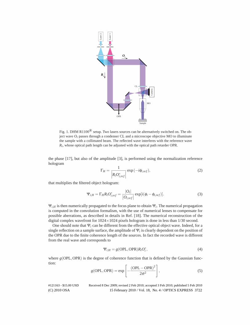
Figure 1 presents the basic configuration of the dual-wavelength DHM used for the experi-mental validation and demonstration of the DHM reflectometry. This DHM (DHM R1100®
from Lyncee Tec) has two different wavelength sources (682.5 nm and 660 nm, with respec-tive coherence length (Lc) of 300 μm and 600 μm, that can be switched on and off alternatelyto provide two different 1024×1024 pixels holograms recorded on the CCD camera, resultingfrom the interference between the reference wave and the object wave reflected by the spec-imen. Usually, dual-wavelength DHM is used to increase the vertical measurement range byan extension of the phase ambiguity-free phase measurement range obtained on homogeneousmaterial and single reflection samples [14]. This ambiguity can also appear for multiple re-flections. Furthermore, a dual-wavelength DHM doubles the equation numbers for the fittingprocedure explained further. A microscope objective (MO) is used to improve the lateral res-olution (LR), that is diffraction limited and depends on the numerical aperture (NA) of MO(LR= 0.61λ/NA) as in classical microscopy [15]. All results in this paper are achieved witha 10× MO (NA= 0.3) that gives a lateral resolution about 1.4μm. The condenser lens (CL inFig. 1) focalizes the wave near the back focal plane of the MO to deliver a collimated illuminat-ing wave Ψill . The optical path length (OPL) of the reference wave is adjusted by moving theoptical path retarder (OPR). The maximal coherence plane, defined in Fig. 2, is placed on thesample surface at the position x0 = 0 by calibrating the position of the OPR to have a maximalfringe contrast when the surface of a calibration mirror is focalized.
3. Complex wavefront measurement
For each wavelength λi, the hologram intensities are
IHi = |Ri|2 + |Oi|2 +RiO∗i +R∗
i Oi, (1)
where Ri and Oi are respectively the reference and object waves for the wavelength λi. Thesedigital holograms are filtered in the spatial frequency domain by using the technique explainedin details in Ref. [16], to retain the real image term RiO∗
i (in reflection it corresponds to thetopographic contrast, a hole giving a phase decrease).
Due to the finite coherence length of the source and due to non-perfecting homogeneousreference and object waves intensities on the CCD, the reconstructed amplitude is not homoge-neous in the field of view when using a standard reconstruction. Therefore, a spatial amplitudenormalization is performed using a reference hologram recorded on a flat reference surface(mirror) as specimen. This hologram is filtered to keep its RiO∗
i,re f term. The normalization of
#121163 - $15.00 USD Received 8 Dec 2009; revised 2 Feb 2010; accepted 3 Feb 2010; published 5 Feb 2010
(C) 2010 OSA 15 February 2010 / Vol. 18, No. 4 / OPTICS EXPRESS 3721
Cam
era
Sample
MO
Ri
Oi
Lase
r 2
Lase
r 1
OPR
CL
Fig. 1. DHM R1100® setup. Two lasers sources can be alternatively switched on. The ob-ject wave Oi passes through a condenser CL and a microscope objective MO to illuminatethe sample with a collimated beam. The reflected wave interferes with the reference waveRi, whose optical path length can be adjusted with the optical path retarder OPR.
the phase [17], but also of the amplitude [3], is performed using the normalization referencehologram
ΓH =1
∣∣∣RiO∗
i,re f
∣∣∣
exp(−iφi,re f ), (2)
that multiplies the filtered object hologram:
Ψi,H = ΓHRiO∗i,re f =
|Oi|∣∣Oi,re f
∣∣
exp[i(φi −φi,re f )]. (3)
Ψi,H is then numerically propagated to the focus plane to obtain Ψi. The numerical propagationis computed in the convolution formalism, with the use of numerical lenses to compensate forpossible aberrations, as described in details in Ref. [18]. The numerical reconstruction of thedigital complex wavefront for 1024×1024 pixels hologram is done in less than 1/30 second.
One should note that Ψi can be different from the effective optical object wave. Indeed, for asingle reflection on a sample surface, the amplitude of Ψi is clearly dependent on the position ofthe OPR due to the finite coherence length of the sources. In fact the recorded wave is differentfrom the real wave and corresponds to
Ψi,H = g(OPL,OPR)RiO∗i , (4)
where g(OPL,OPR) is the degree of coherence function that is defined by the Gaussian func-tion:
g(OPL,OPR) = exp
[
− (OPL−OPR)2
2σ2
]
, (5)
#121163 - $15.00 USD Received 8 Dec 2009; revised 2 Feb 2010; accepted 3 Feb 2010; published 5 Feb 2010
(C) 2010 OSA 15 February 2010 / Vol. 18, No. 4 / OPTICS EXPRESS 3722
0.4
0.6
0.8
1
Ψill
Ψ0 Ψ1 Ψ2 Ψ3
g(OPL,OPR)
n0
n1
n2
n3
d1
d2
d3
0
x0
α
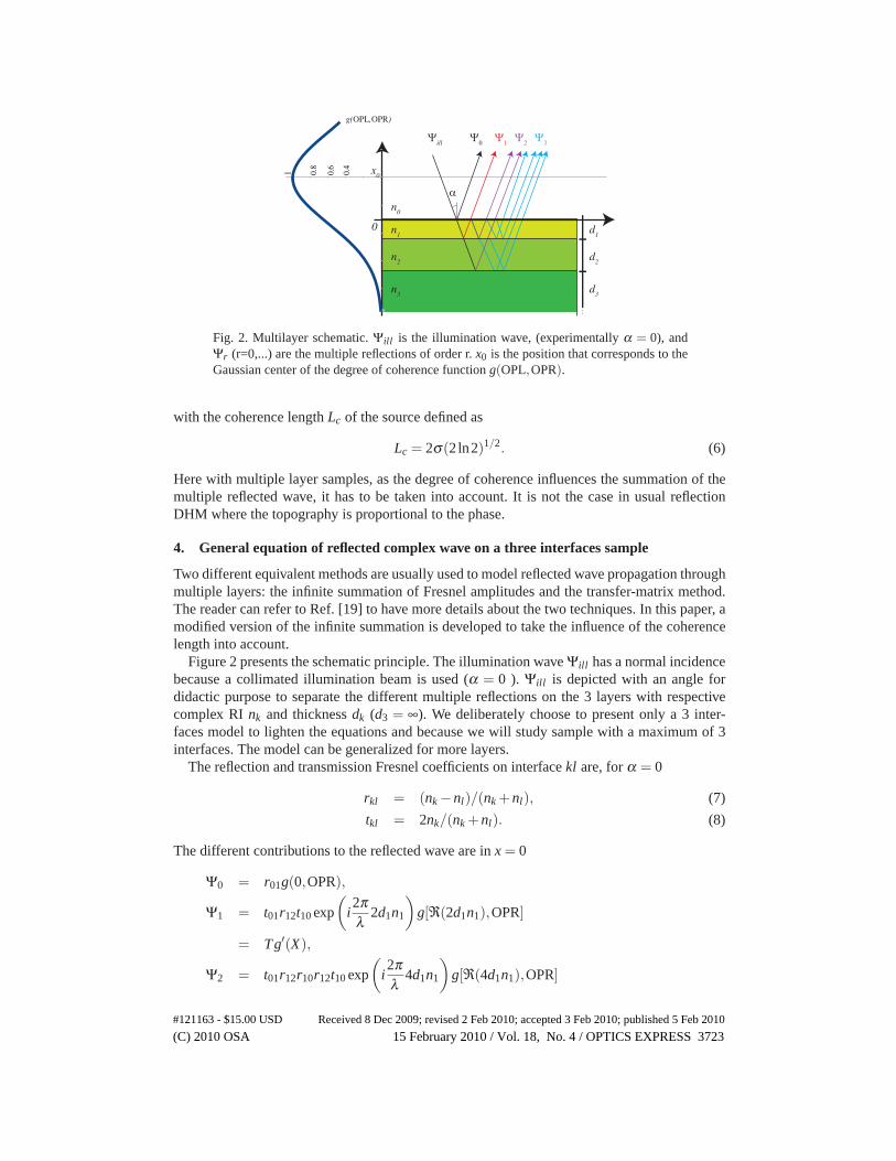
Fig. 2. Multilayer schematic. Ψill is the illumination wave, (experimentally α = 0), andΨr (r=0,...) are the multiple reflections of order r. x0 is the position that corresponds to theGaussian center of the degree of coherence function g(OPL,OPR).
with the coherence length Lc of the source defined as
Lc = 2σ(2ln2)1/2. (6)
Here with multiple layer samples, as the degree of coherence influences the summation of themultiple reflected wave, it has to be taken into account. It is not the case in usual reflectionDHM where the topography is proportional to the phase.
4. General equation of reflected complex wave on a three interfaces sample
Two different equivalent methods are usually used to model reflected wave propagation throughmultiple layers: the infinite summation of Fresnel amplitudes and the transfer-matrix method.The reader can refer to Ref. [19] to have more details about the two techniques. In this paper, amodified version of the infinite summation is developed to take the influence of the coherencelength into account.
Figure 2 presents the schematic principle. The illumination wave Ψill has a normal incidencebecause a collimated illumination beam is used (α = 0 ). Ψill is depicted with an angle fordidactic purpose to separate the different multiple reflections on the 3 layers with respectivecomplex RI nk and thickness dk (d3 = ∞). We deliberately choose to present only a 3 inter-faces model to lighten the equations and because we will study sample with a maximum of 3interfaces. The model can be generalized for more layers.
The reflection and transmission Fresnel coefficients on interface kl are, for α = 0
rkl = (nk −nl)/(nk +nl), (7)
tkl = 2nk/(nk +nl). (8)
The different contributions to the reflected wave are in x = 0
Ψ0 = r01g(0,OPR),
Ψ1 = t01r12t10 exp
(
i2πλ
2d1n1
)
g[ℜ(2d1n1),OPR]
= Tg′(X),
Ψ2 = t01r12r10r12t10 exp
(
i2πλ
4d1n1
)
g[ℜ(4d1n1),OPR]
#121163 - $15.00 USD Received 8 Dec 2009; revised 2 Feb 2010; accepted 3 Feb 2010; published 5 Feb 2010
(C) 2010 OSA 15 February 2010 / Vol. 18, No. 4 / OPTICS EXPRESS 3723
+ t01t12r23t21t10 exp
[
i2πλ
(2d1n1 +2d2n2)]
g[ℜ(2d1n1 +2d2n2),OPR]
= ATg′(2X)+BTg′(X +Y ),
Ψ3 = t01r12r10r12r10r12t10 exp
(
i2πλ
6d1n1
)
g[ℜ(6d1n1),OPR]
+ t01r12r10t12r23t21t10 exp
[
i2πλ
(4d1n1 +2d2n2)]
g[ℜ(4d1n1 +2d2n2),OPR]
+ t01t12r23t21r10r12t10 exp
[
i2πλ
(4d1n1 +2d2n2)]
g[ℜ(4d1n1 +2d2n2),OPR]
+ t01t12r23r21r23t21t10 exp
[
i2πλ
(2d1n1 +4d2n2)]
g[ℜ(2d1n1 +4d2n2),OPR]
= A2Tg′(3X)+ABTg′(2X +Y )+BCTg′(2X +Y )+BDTg′(X +2Y ), (9)
where ℜ is the complex real part, T = t01r12t10, OPR = 2x0n0, g′(x) =g[ℜ(x),OPR]exp
[
i 2πλ (x)
]
, X = 2d1n1, Y = 2d2n2, A = r12r10, B = t12r23t21/r12, C = r10r12
and D = r21r23. One can note that a simple rule allows deducing the component Ψr+1 from Ψr:
Ψr → Ψr+1
...ATg′(mX +nY ) →{
...AATg′[(m+1)X +nY ]
...ABTg′[mX +(n+1)Y ]
...BTg′(mX +nY ) →{
...BCTg′[(m+1)X +nY ]
...BDTg′[mX +(n+1)Y ]
...CTg′(mX +nY ) →{
...CATg′[(m+1)X +nY ]
...CBTg′[mX +(n+1)Y ]
...DTg′(mX +nY ) →{
...DCTg′[(m+1)X +nY ]
...DDTg′[mX +(n+1)Y ] (10)
The wavefront in x = x0 is therefore:
Ψ(d,n,x0) =
[N
∑r=0
Ψr exp
(
i2πλ
2x0n0
)]∗=
N
∑r=0
Ψ∗r exp
(
−i2πλ
2x0n0
)
(11)
where d = [d1,d2] and n = [n0,n1,n2,n3]. One can note the complex conjugate operator in thesummation, in order to stay consistent with the real image term reconstruction.
5. Models and fitting procedure
The previous section presents the general function of the wave reflected on a three interfacessample. But for each point of a micro-structure, the parameters of this function could be dif-ferent, and a model of the micro-structure has to be defined. In the next sections, we presenttwo different example of micro-structures model: steps deposition on a single layer wafer, andetching on 3 interfaces samples. These models, combined with fitting procedure, allow themeasurement of topographic image of two home-made SiO2 /Si test targets and SIMS sputtercraters in multiple interface sample.
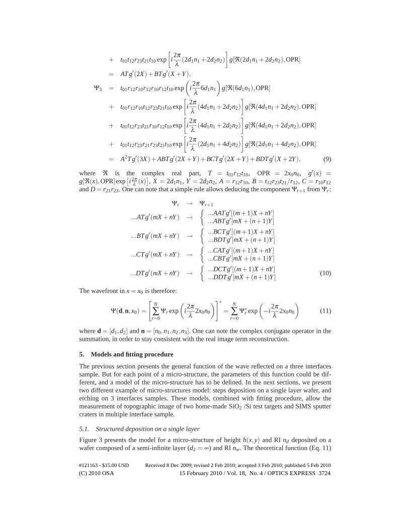
5.1. Structured deposition on a single layer
Figure 3 presents the model for a micro-structure of height h(x,y) and RI nd deposited on awafer composed of a semi-infinite layer (d2 = ∞) and RI nw. The theoretical function (Eq. 11)
#121163 - $15.00 USD Received 8 Dec 2009; revised 2 Feb 2010; accepted 3 Feb 2010; published 5 Feb 2010
(C) 2010 OSA 15 February 2010 / Vol. 18, No. 4 / OPTICS EXPRESS 3724
n0
0x0
d1(x,y)
d2
0’0’’
Ψ[d(x,y),n(x,y),x0(x,y)]Ψill
nd
nw
hj
Fig. 3. Model for structures of height h(x,y) and RI nd deposited on a semi-infinite wafer(d2 = ∞) with RI nw. The multiple layers function (Eq. 11) is defined from the respectiveorigin 0, 0’ and so on, for each step.
is now adapted to this model. For each position (x,y) of the sample, the reflected wavefront is
Ψ(x,y) = Ψ[d(x,y),n(x,y),x0(x,y)] (12)
where the different parameters depend on the deposit thickness h(x,y):
d(x,y) = [h(x,y),∞] (13)
n(x,y) ={
[n0,nw,0,0] if h(x,y) = 0[n0,nd ,nw,0] if h(x,y) > 0
(14)
x0(x,y) = −h(x,y). (15)
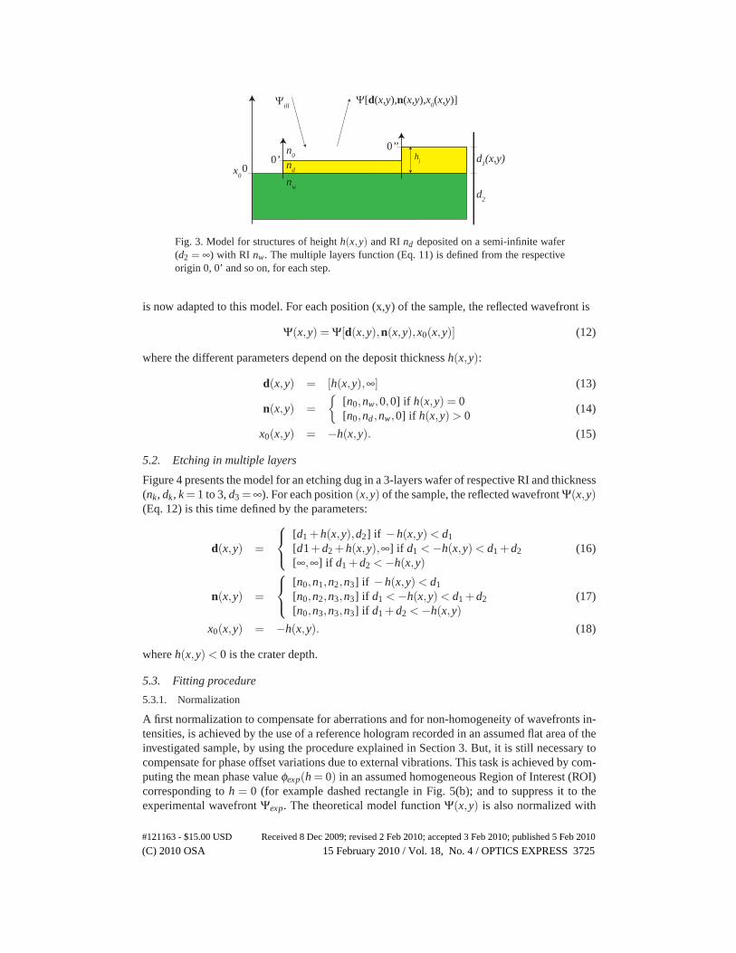
5.2. Etching in multiple layers
Figure 4 presents the model for an etching dug in a 3-layers wafer of respective RI and thickness(nk, dk, k = 1 to 3, d3 = ∞). For each position (x,y) of the sample, the reflected wavefront Ψ(x,y)(Eq. 12) is this time defined by the parameters:
d(x,y) =
⎧
⎨
⎩
[d1 +h(x,y),d2] if −h(x,y) < d1
[d1+d2 +h(x,y),∞] if d1 < −h(x,y) < d1 +d2
[∞,∞] if d1 +d2 < −h(x,y)(16)
n(x,y) =
⎧
⎨
⎩
[n0,n1,n2,n3] if −h(x,y) < d1
[n0,n2,n3,n3] if d1 < −h(x,y) < d1 +d2
[n0,n3,n3,n3] if d1 +d2 < −h(x,y)(17)
x0(x,y) = −h(x,y). (18)
where h(x,y) < 0 is the crater depth.
5.3. Fitting procedure
5.3.1. Normalization
A first normalization to compensate for aberrations and for non-homogeneity of wavefronts in-tensities, is achieved by the use of a reference hologram recorded in an assumed flat area of theinvestigated sample, by using the procedure explained in Section 3. But, it is still necessary tocompensate for phase offset variations due to external vibrations. This task is achieved by com-puting the mean phase value φexp(h = 0) in an assumed homogeneous Region of Interest (ROI)corresponding to h = 0 (for example dashed rectangle in Fig. 5(b); and to suppress it to theexperimental wavefront Ψexp. The theoretical model function Ψ(x,y) is also normalized with
#121163 - $15.00 USD Received 8 Dec 2009; revised 2 Feb 2010; accepted 3 Feb 2010; published 5 Feb 2010
(C) 2010 OSA 15 February 2010 / Vol. 18, No. 4 / OPTICS EXPRESS 3725
n0
n1
n2
n3
0x
0
d1
d2
x,y
h(x,y)
hmin
I II III IV V
d3
Fig. 4. Etching dug in 3-layers wafer model. The maximum coherence position is x0 = 0.The etching is delimited by 5 different areas (I,V: outside crater; II and IV crater edges; andIII maximum depth). The layers are defined by the RIs nk and thicknesses dk.
the complex value computed for h = 0. The normalized experimental and theoretical functionsare:
Ψexp(x,y) = Ψexp(x,y)exp[−iφexp(h = 0)], (19)
Ψ(x,y) =Ψ(x,y)
Ψ(h = 0). (20)
5.3.2. Mean square fitting
For a given type of sample, the normalized theoretical functions Ψi (i=1,2 for respectivelyλ1 and λ2) are defined by the thicknesses and RIs. These parameters can be either a prioriknown constants or the results of a previous fitting procedure. Furthermore, some parametersare assumed to be identical in the entire field of view (for example thickness and RIs), oncontrary to the topography (deposit structure height, etching depth) that depends on the position(x,y). Therefore, to determine the unknown parameters, 2S experimental data points (Ψi,exp)(S for each wavelength) are fitted by minimizing the sum of errors between theoretical andexperimental complex data (errors corresponds to the distances between the complex vectors inthe complex plane):
MSE =2
∑i=1
S
∑j=1
∣∣Ψi j − Ψi j,exp(d,n)
∣∣ , (21)
where the subscript i j correspond to the wavelength λi and the step j. MSE is therefore the meansquare error of the fit. It implies that the system has to be determined or overdetermined to finda solution. Therefore, it is not possible, in the most general cases, to compute all the parameters.But in most of the cases, several parameters can be computed as it will be demonstrated in thenext sections.
As fitting procedures are time consuming tasks and as RIs and thickness layers can be con-sidered most of the time as constant, the mean square fitting is achieved by only taking intoaccount complex data averaged over selected ROIs. These constants then allow computing thetopography for each image pixel by using the next procedure. One has to note that, constant
5.3.3. Topographic image
When RIs and layer thicknesses are assumed to be known constants on the entire field of view(known sample characteristics or fitting results), the theoretical complex functions Ψi(h) arecomputed with h = hmin + pΔh, p = 0,N (Δh defines the precision, hmin the minimal height, Nthe number of points). Then for each reconstructed pixel (x,y), the height h(x,n) is defined asthe abscissa that corresponds to the minimum of the function ∑2
i=1
∣∣Ψi(h)− Ψi,exp(x,y)
∣∣.
#121163 - $15.00 USD Received 8 Dec 2009; revised 2 Feb 2010; accepted 3 Feb 2010; published 5 Feb 2010
(C) 2010 OSA 15 February 2010 / Vol. 18, No. 4 / OPTICS EXPRESS 3726
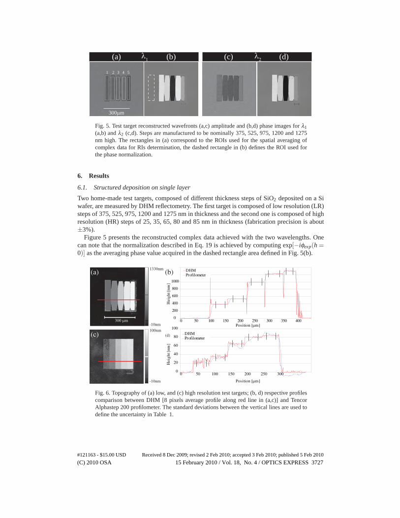
(a) (b) (c) (d)
300μm
1 2 3 4 5
λ1 λ2
Fig. 5. Test target reconstructed wavefronts (a,c) amplitude and (b,d) phase images for λ1(a,b) and λ2 (c,d). Steps are manufactured to be nominally 375, 525, 975, 1200 and 1275nm high. The rectangles in (a) correspond to the ROIs used for the spatial averaging ofcomplex data for RIs determination, the dashed rectangle in (b) defines the ROI used forthe phase normalization.
6. Results
6.1. Structured deposition on single layer
Two home-made test targets, composed of different thickness steps of SiO2 deposited on a Siwafer, are measured by DHM reflectometry. The first target is composed of low resolution (LR)steps of 375, 525, 975, 1200 and 1275 nm in thickness and the second one is composed of highresolution (HR) steps of 25, 35, 65, 80 and 85 nm in thickness (fabrication precision is about±3%).
Figure 5 presents the reconstructed complex data achieved with the two wavelengths. Onecan note that the normalization described in Eq. 19 is achieved by computing exp[−iφexp(h =0)] as the averaging phase value acquired in the dashed rectangle area defined in Fig. 5(b).
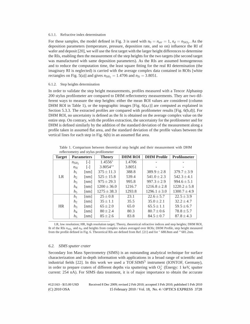
Hei
ght [
nm]
(a) (b)
-10nm
1330nm
300 μm
Hei
ght [
nm]
-10nm
100nm(c) (d)
0 50 100 150 200 250 300 350 4000
200
400
600
800
1000
DHMProfilometer
0 50 100 150 200 250 3000
20
40
60
80
100DHMProfilometer
Position [μm]
Position [μm]
Fig. 6. Topography of (a) low, and (c) high resolution test targets; (b, d) respective profilescomparison between DHM [8 pixels average profile along red line in (a,c)] and TencorAlphastep 200 profilometer. The standard deviations between the vertical lines are used todefine the uncertainty in Table 1.
#121163 - $15.00 USD Received 8 Dec 2009; revised 2 Feb 2010; accepted 3 Feb 2010; published 5 Feb 2010
(C) 2010 OSA 15 February 2010 / Vol. 18, No. 4 / OPTICS EXPRESS 3727
6.1.1. Refractive index determination
For these samples, the model defined in Fig. 3 is used with n0 = nair = 1, nd = nSiO2 . As thedeposition parameters (temperature, pressure, deposition rate, and so on) influence the RI ofwafer and deposit [20], we will use the first target with the larger height differences to determinethe RIs, enabling then the measurement of the step heights for the two targets (the second targetwas manufactured with same deposition parameters). As the RIs are assumed homogeneousand to reduce the computation time, the least square fitting for the real RI determination (theimaginary RI is neglected) is carried with the average complex data contained in ROIs [whiterectangles on Fig. 5(a)] and gives nSi02 = 1.4706 and nSi = 3.8051.
6.1.2. Step heights determination
In order to validate the step height measurements, profiles measured with a Tencor Alphastep200 stylus profilometer are compared to DHM reflectometry measurements. They are two dif-ferent ways to measure the step heights: either the mean ROI values are considered (columnDHM ROI in Table 1), or the topographic images [Fig. 6(a,c)] are computed as explained inSection 5.3.3. The extracted profiles are compared with profilometer results [Fig. 6(b,d)]. ForDHM ROI, no uncertainty is defined as the fit is obtained on the average complex value on theentire step. On contrary, with the profiles extraction, the uncertainty for the profilometer and forDHM is defined similarly by the addition of the standard deviation of the measurement along aprofile taken in assumed flat area, and the standard deviation of the profile values between thevertical lines for each step in Fig. 6(b) in an assumed flat area.
Table 1. Comparison between theoretical step height and their measurement with DHMreflectometry and stylus profilometer
Target Parameters Theory DHM ROI DHM Profile ProfilometernSi02 [-] 1.4556∗ 1.4706 - -nSi [-] 3.8054∗∗ 3.8051 - -h1 [nm] 375±11.3 388.8 389.9±2.8 379.7±3.9
LR h2 [nm] 525±15.8 539.4 541.0±2.3 542.3±4.1h3 [nm] 975±29.3 995.8 997.3±2.9 994.6±5.1h4 [nm] 1200±36.0 1216.7 1216.8±2.8 1220.2±5.8h5 [nm] 1275±38.3 1293.8 1296.1±3.0 1300.7±4.9h1 [nm] 25±0.8 23.1 22.6±5.7 22.5±3.9h2 [nm] 35±1.1 35.5 35.0±2.1 32.2±4.7
HR h3 [nm] 65±2.0 65.0 65.5±1.1 59.5±6.7h4 [nm] 80±2.4 80.3 80.7±0.6 78.8±5.7h5 [nm] 85±2.6 83.8 84.5±0.7 87.8±4.3
LR, low resolution; HR, high resolution target; Theory, theoretical refractive indices and step heights; DHM ROI,fit of the RIs nSi02 and nSi and heights from complex values averaged over ROIs; DHM Profile, step height measuredfrom the profile defined in Fig. 6. Theoretical RIs are defined from Ref. [21] and for ∗ 688.8nm and ∗∗681.2nm.
6.2. SIMS sputter crater
Secondary Ion Mass Spectrometry (SIMS) is an outstanding analytical technique for surfacecharacterization and in-depth information with applications in a broad range of scientific andindustrial fields [22]. In this work we used a TOF.SIMS5 instrument (IONTOF, Germany),in order to prepare craters of different depths via sputtering with O+
2 (Energy: 1 keV, sputtercurrent: 254 nA). For SIMS data treatment, it is of major importance to obtain the accurate
#121163 - $15.00 USD Received 8 Dec 2009; revised 2 Feb 2010; accepted 3 Feb 2010; published 5 Feb 2010
(C) 2010 OSA 15 February 2010 / Vol. 18, No. 4 / OPTICS EXPRESS 3728
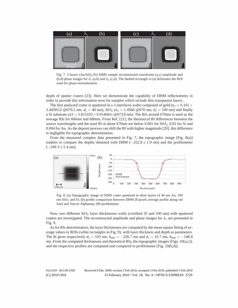
300μm
(a) (b) (c) (d)λ1 λ2
Fig. 7. 3-layers (Au/SiO2/Si) SIMS sample reconstructed wavefronts (a,c) amplitude and(b,d) phase images for λ1 (a,b) and λ2 (c,d). The dashed rectangle in (a) delineates the ROIused for phase normalization.
depth of sputter craters [23]. Here we demonstrate the capability of DHM reflectometry inorder to provide this information even for samples which include thin transparent layers.
The first analyzed crater is sputtered in a 3 interfaces wafer composed of gold (n1 = 0.161+3.445812i @670.2 nm, d1 = 40 nm), SiO2 (n2 = 1.4560 @670 nm, d2 = 100 nm) and finallya Si substrate (n3 = 3.815103+0.014041i @673.8 nm). The RIs around 670nm is used as theaverage RIs for 660nm and 680nm. From Ref. [21], the theoretical RI differences between thesource wavelengths and the used RI at about 670nm are below 0.001 for SiO2, 0.02 for Si and0.004 for Au. As the deposit process can shift the RI with higher magnitude [20], this differenceis negligible for topographic determination.
From the measured complex data presented in Fig. 7, the topographic image [Fig. 8(a)]enables to compare the depths obtained with DHM (−252.8± 1.9 nm) and the profilometer(−249.3±5.4 nm).
0 100 200 300 400 500 600 700 800 900-300
-250
-200
-150
-100
-50
0
50
DHMProf ilometer
Position [μm]
Hei
ght [
nm]
(a) (b)
-260nm
10nm
100 μm
Fig. 8. (a) Topographic image of SIMS crater sputtered in three layers of 40 nm Au, 100nm SiO2 and Si; (b) profile comparison between DHM [8 pixels average profile along redline] and Tencor Alphastep 200 profilometer.
Now, two different SiO2 layer thicknesses wafer (certified 35 and 100 nm) with sputteredcraters are investigated. The reconstructed amplitude and phase images for λ1 are presented inFig. 9.
As for RIs determination, the layer thicknesses are computed by the mean square fitting of av-erage values in ROIs (white rectangles in Fig. 9), with layer thickness and depth as parameters.The fit gives respectively d1 = 103 nm, hmin = −226.7 nm and d1 = 33.7 nm, hmin = −148.8nm. From the computed thicknesses and theoretical RIs, the topographic images [Figs. 10(a,c)],and the respective profiles are computed and compared to profilometer [Fig. 10(b,d)].
#121163 - $15.00 USD Received 8 Dec 2009; revised 2 Feb 2010; accepted 3 Feb 2010; published 5 Feb 2010
(C) 2010 OSA 15 February 2010 / Vol. 18, No. 4 / OPTICS EXPRESS 3729
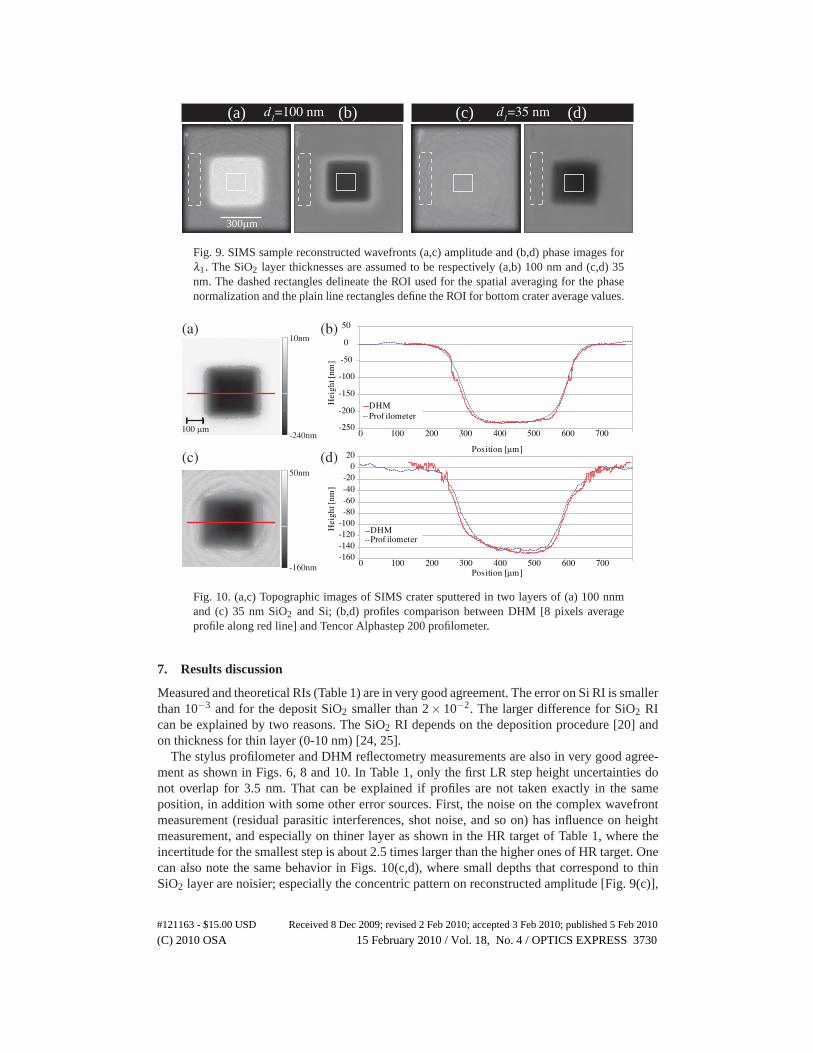
300μm
(a) (b) (c) (d)d1=100 nm d
1=35 nm
Fig. 9. SIMS sample reconstructed wavefronts (a,c) amplitude and (b,d) phase images forλ1. The SiO2 layer thicknesses are assumed to be respectively (a,b) 100 nm and (c,d) 35nm. The dashed rectangles delineate the ROI used for the spatial averaging for the phasenormalization and the plain line rectangles define the ROI for bottom crater average values.
0 100 200 300 400 500 600 700-250
-200
-150
-100
-50
0
50
DHMProf ilometer
Position [μm]
Hei
ght [
nm]
(a) (b)
-240nm
10nm
100 μm
Position [μm]
Hei
ght [
nm]
-160nm
50nm
(c) (d)
0 100 200 300 400 500 600 700-160-140-120-100-80-60-40-20
020
DHMProf ilometer
Fig. 10. (a,c) Topographic images of SIMS crater sputtered in two layers of (a) 100 nnmand (c) 35 nm SiO2 and Si; (b,d) profiles comparison between DHM [8 pixels averageprofile along red line] and Tencor Alphastep 200 profilometer.
7. Results discussion
Measured and theoretical RIs (Table 1) are in very good agreement. The error on Si RI is smallerthan 10−3 and for the deposit SiO2 smaller than 2× 10⁻². The larger difference for SiO2 RIcan be explained by two reasons. The SiO2 RI depends on the deposition procedure [20] andon thickness for thin layer (0-10 nm) [24, 25].
The stylus profilometer and DHM reflectometry measurements are also in very good agree-ment as shown in Figs. 6, 8 and 10. In Table 1, only the first LR step height uncertainties donot overlap for 3.5 nm. That can be explained if profiles are not taken exactly in the sameposition, in addition with some other error sources. First, the noise on the complex wavefrontmeasurement (residual parasitic interferences, shot noise, and so on) has influence on heightmeasurement, and especially on thiner layer as shown in the HR target of Table 1, where theincertitude for the smallest step is about 2.5 times larger than the higher ones of HR target. Onecan also note the same behavior in Figs. 10(c,d), where small depths that correspond to thinSiO2 layer are noisier; especially the concentric pattern on reconstructed amplitude [Fig. 9(c)],
#121163 - $15.00 USD Received 8 Dec 2009; revised 2 Feb 2010; accepted 3 Feb 2010; published 5 Feb 2010
(C) 2010 OSA 15 February 2010 / Vol. 18, No. 4 / OPTICS EXPRESS 3730
coming from a parasitic interference, gives an important contribution in the reconstructed depthfield [Fig. 10(c)]. This problem is inherent to the DHM setup configuration. Reduced coherencelength, small misalignment of optics or numerical spatial filtering could permit to avoid mostof these parasitic interferences. Nevertheless, it is very difficult to avoid all of them, especiallyfor a DHM microscope configured with a turret of several magnification MO.
Secondly, an error on the RI determination for the reasons previously given, contributes alsoto a mismatch between real and measured heights. This effect could also explain the abrupt andnoisier transition near layer interfaces in graphs (c,d) of Figs. 8 and 10. Finally, the non disper-sion assumption and normal incident wave contributes to increase the uncertainty. An advantageof DHM can be seen in Fig. 6(d), where step edges are sharper for DHM reflectometry than forprofilometer. Indeed the stylus tip size induces rounded edges transition. Furthermore, DHMhas the advantage to avoid mechanical calibration to convert detected signal in height, on con-trary of profilometer or AFM instruments; DHM calibration depends only on the wavelengthsources.
Finally, the measured layer thicknesses of SiO2 from the SIMS sample (Fig. 10) coincidevery well with the certified values (33.7 nm and 103 nm for 35 nm and 100 nm certification).The difference can be explained by the same arguments as before: complex data noise, mis-match between real and used RI.
One notes that the DHM reflectometry principle is demonstrated for a small magnificationMO (10×). For higher magnification, the basic principle is still valid if the illumination wavecould still be assumed collinear. If this assumption could not be satisfied, the incident anglesshould be in the theoretical equation. Furthermore, for high NA, the depth-of-focus (DOF)limits the precision for layer thickness larger or near the DOF. Indeed, the waves reflectedfrom interfaces out of DEF gives an out-of-focus contribution that can be eventually shiftedcompared to the first interface if the sample is not perpendicular to the optical axis.
Next improvements for DHM reflectometry will be to introduce dispersion and incident an-gles in the theoretical equation, in particular for high magnification application. Furthermore,simultaneous dual-wavelength DHM will allow to obtained real-time measurements. Three ormore wavelengths will also permit to increase the number of equations and therefore the num-bers of unknown parameters to fit simultaneously, in particular the thickness for all layers.Obviously, the increase of unknown parameters, for a given number of equations, increases thefitting time consuming exponentially and decreases the precision on the fitting parameters.
8. Conclusion
These results show that DHM reflectometry allows full field topographic thickness of semi-transparent layers micro-structures, with a resolution better than 2 nm for layer larger than20-30 nm. Furthermore, we demonstrate that DHM reflectometry allows RIs determinationwith a precision better than 2×10⁻² for the deposited material RI and 1×10⁻³ for the waferRI. With this new DHM measurement modality, surface topography of both homogeneous andnon-homogeneous material samples are measured precisely. This opens new application fieldsfor DHM, like thin films and multiple material specimen investigation.
Acknowledgments
The research leading to these results has received funding from the European Community’sSeventh Framework Programme FP7/2007-2013 under grant agreement no 216105. The authorsthank Bamdad Afra from the Advanced Photonics Laboratory in EPFL (Ecole PolytechniqueFederale de Lausanne) for the delivery of the stylus profilometer measurements. Ahmet AtaAkatay is supported by the CCMX NMMC grant: ”Study of complex interfacial propertieswith nanoscale resolution optical microscopy”.
#121163 - $15.00 USD Received 8 Dec 2009; revised 2 Feb 2010; accepted 3 Feb 2010; published 5 Feb 2010
(C) 2010 OSA 15 February 2010 / Vol. 18, No. 4 / OPTICS EXPRESS 3731


