Embed Size (px)
Citation preview

arX
iv:c
ond-
mat
/001
2179
v2 [
cond
-mat
.str
-el]
9 M
ay 2
001
Determination of the (3×3)-Sn/Ge(111) structure by photoelectron diffraction.
L. Petaccia,a L. Floreano,a,∗ M. Benes,a,b D. Cvetko,a,c,d A. Goldoni,c L. Grill,a A. Morgante,a,b A. Verdini,a and S.Modestia,b
a Laboratorio TASC, Istituto Nazionale per la Fisica della Materia, Basovizza SS14 Km 163.5, I-34012 Trieste, Italyb Department of Physics, University of Trieste, Via Valerio 2, I-34100 Trieste, Italy
c Sincrotrone Trieste SCpA, Basovizza SS14 Km 163.5, I-34012 Trieste, Italyd Jozef Stefan Institute, Department of Physics, Ljubljana University, Ljubljana, Slovenia
The bonding geometry of Sn on Ge(111) has been quantitatively determined for the (3×3) phase at150 K. Energy scan photoelectron diffraction of the Sn 4d core levels has been used to independentlymeasure the bond length between Sn and its nearest neighbour Ge atoms and the vertical distancebetween Sn and the Ge atom beneath. This latter distance is found to be ∼ 0.3 A larger for one Snatom out of the three contained in the lattice unit cell. The bond lengths and the bond directions,obtained by the angular scans, are found to be practically the same for the three Sn atoms within± 0.03 A and ± 3◦, respectively. The three nearest neighbour Ge atoms thus partially follow theSn atom in its vertical ripple.
PACS numbers: 61.14Qp, 79.60Dp, 68.35Bs
∗Corresponding Author: Luca Floreano, Surface Division, Laboratorio TASC-INFM, Basovizza, SS14 Km 163.5 I-34012Trieste, Italy. E-mail: [email protected]
1
I. INTRODUCTION
At a coverage of about 1/3 monolayer (ML), Sn and Pbdeposited on Ge(111) below ∼ 550 K form a metastable
(√
3×√
3)R30◦ phase, where the Sn or Pb atoms occupyT4 sites above the Ge lattice. This phase continuouslyand reversibly transforms into a (3 × 3) one, upon cool-ing below ∼ 200 K. This new phase was first observedby scanning tunneling microscopy (STM) on the Pb/Geand Sn/Ge systems and attributed to the manifestationof a surface charge density wave (CDW).1–3 The natureof this phase transition is still an open issue, also becauseof the controversal determination of the atomic structureof the two phases.4–6 The low temperature (3× 3) phaseis formed by three inequivalent Sn atoms per unit cell.X-ray diffraction (XRD) and low energy electron diffrac-tion (LEED) experiments now consistently point to anatomic structure where one Sn atom out of three pro-trudes above the surface.5,7 A vertical ripple of ∼ 0.3 A isthus observed between the Sn atoms of the surface unitcell. Within the CDW model the inequivalence betweenthe Sn atoms should disappear in the room temperature(RT) (
√3×
√3) phase. This is consistent with the most
recent experiments that indicate equivalent Sn atoms atthe same height level in the adatom layer at RT.5,7
X-ray photoemission spectroscopy (XPS) experimentson the (3 × 3) phase indeed show two Sn 4d core leveldoublets split by ∼ 0.4 eV, with an intensity ratio ofapproximately 2:1 between the two components (A andB, majority and minority components, respectively),8–10
thus indicating two different kinds of Sn atoms. Thisspectrum remains practically unchanged throughout thephase transition.8,9,11 This opens the way to alternativeexplanations, such as dynamical fluctuations11 and order-disorder phase transitions,9 where the local structure ofthe two phases is the same. Very recently the stronginfluence on the phase transition of small defect concen-tration has been put in evidence.12,13 Recently publishedXPS studies14 suggest that, at exactly 1/3 ML coverage,the Sn 4d spectrum is different from that reported in theliterature up to now. In particular the spectrum wouldshow an intensity ratio between the A and B compo-nent appreciably different from that reported in previousworks and would have an additional component in thehigh temperature (
√3×
√3) phase. These findings were
used to support the CDW model.It is therefore important to determine the exact line-
shape of the Sn 4d spectrum and to measure the (3 × 3)structure by XPS experiments on the single Sn core levelcomponents in order to check its consistency with thatobtained by XRD and to identify the bonding sites of theatoms contributing to the majority and minority compo-nents. We have thus performed photoelectron diffrac-tion (PED) measurements of the Sn 4d core levels at theALOISA beamline (Elettra Synchrotron). The wide va-riety of scattering geometries accessible at the ALOISAend station allowed us to measure separately the bond di-
rection and length between the Sn adatom and its threenearest neighbour Ge atoms (Genn) and the Sn verticaldistance to the next nearest neighbour Ge atom beneath(Gennn). In a previous paper we qualitatively reportedon the preliminary experimental results, i.e. the substan-tial equivalence of the Sn–Genn bond angle and lengthfor both A and B type Sn atoms, which mainly differfor their vertical height Sn–Gennn.15 Here we present thequantitative determination of the bonding geometry ofSn atoms in the (3 × 3) unit cell, as obtained by fittingto multiple scattering calculations (MSCD)16 the PEDdata obtained in a more extended energy range and witha better statistics. We attribute each of the two compo-nents of the Sn 4d photoemission spectrum to a specificbonding geometry of the two inequivalent types of Snatoms. To our knowledge, such a direct correlation wasnever extracted before. The rippled structure obtainedin the present work is in good agreement both with previ-ous XRD determinations5,7 and with recent density func-tional calculations (DFT) performed in the local densityapproximation with gradient correction (LDA-GC)17 andin combination with local-orbital (LDA-LO) methods18.
II. EXPERIMENTAL SET-UP AND SAMPLEPREPARATION
The present experiment has been performed in theUHV end station of the ALOISA beamline19,20 at theElettra synchrotron (Trieste). Details about the experi-mental setup and sample cleaning are given elsewhere.15
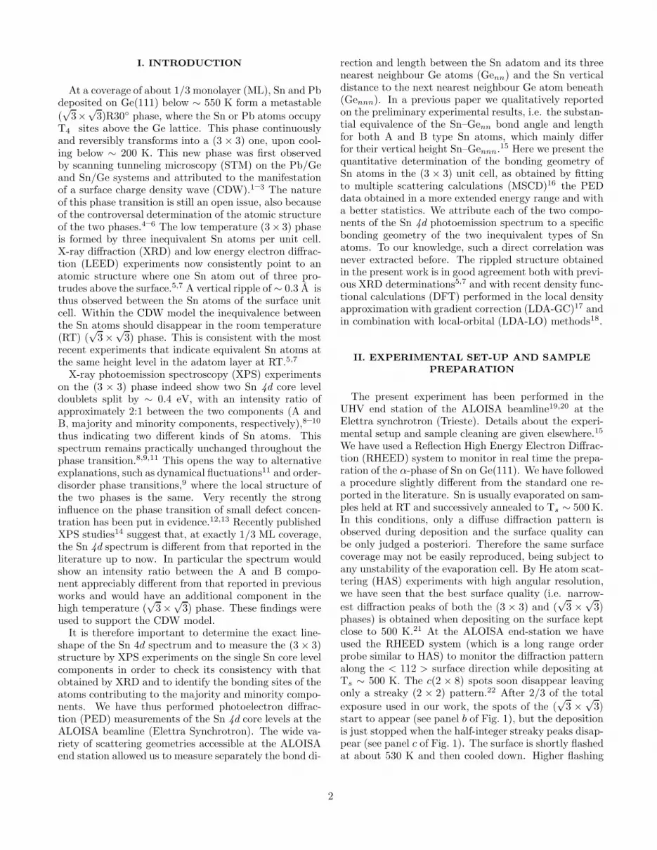
We have used a Reflection High Energy Electron Diffrac-tion (RHEED) system to monitor in real time the prepa-ration of the α-phase of Sn on Ge(111). We have followeda procedure slightly different from the standard one re-ported in the literature. Sn is usually evaporated on sam-ples held at RT and successively annealed to Ts ∼ 500 K.In this conditions, only a diffuse diffraction pattern isobserved during deposition and the surface quality canbe only judged a posteriori. Therefore the same surfacecoverage may not be easily reproduced, being subject toany unstability of the evaporation cell. By He atom scat-tering (HAS) experiments with high angular resolution,we have seen that the best surface quality (i.e. narrow-
est diffraction peaks of both the (3 × 3) and (√
3 ×√
3)phases) is obtained when depositing on the surface keptclose to 500 K.21 At the ALOISA end-station we haveused the RHEED system (which is a long range orderprobe similar to HAS) to monitor the diffraction patternalong the < 112 > surface direction while depositing atTs ∼ 500 K. The c(2 × 8) spots soon disappear leavingonly a streaky (2 × 2) pattern.22 After 2/3 of the total
exposure used in our work, the spots of the (√
3 ×√
3)start to appear (see panel b of Fig. 1), but the depositionis just stopped when the half-integer streaky peaks disap-pear (see panel c of Fig. 1). The surface is shortly flashedat about 530 K and then cooled down. Higher flashing
2
temperature irreversibly leads to a stable (7 × 7) phase,as previously reported23. Shorter exposures never lead tothe complete disappearance of the (2× 2) pattern. After
this procedure sharp spots of the (√
3 ×√
3)R30◦ phaseare observed along the < 112 > direction. To detect thespots characteristic of the (3×3) phase, the RHEED pat-tern was observed along the < 110 > direction, as shownin the d panel of Fig. 1, which is taken at Ts ∼ 150 K.We have seen that no degradation of the photoemissionspectra nor of the RHEED patterns occurs for at least10 hours, when the sample is left inside the experimentalchamber. In any case, a new surface was always preparedafter 10 hours.
The whole set of spectroscopical data hereafter shownhas been taken with constant electron energy resolutionof 170 meV. The photon energy resolution has been al-ways ≤ 150 meV. The overall instrumental resolution isthus ≤ 225 meV.
III. RESULTS AND DISCUSSION
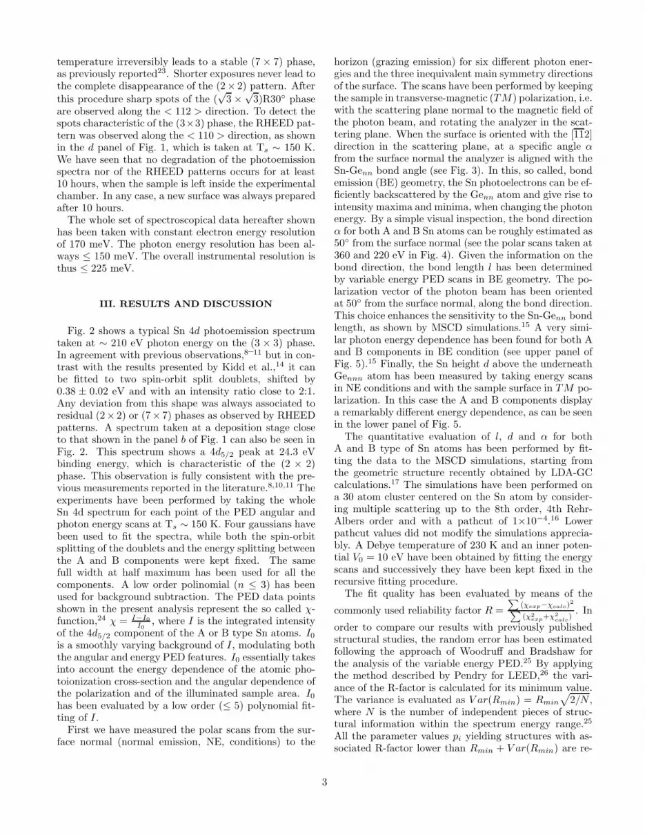
Fig. 2 shows a typical Sn 4d photoemission spectrumtaken at ∼ 210 eV photon energy on the (3 × 3) phase.In agreement with previous observations,8–11 but in con-trast with the results presented by Kidd et al.,14 it canbe fitted to two spin-orbit split doublets, shifted by0.38 ± 0.02 eV and with an intensity ratio close to 2:1.Any deviation from this shape was always associated toresidual (2× 2) or (7× 7) phases as observed by RHEEDpatterns. A spectrum taken at a deposition stage closeto that shown in the panel b of Fig. 1 can also be seen inFig. 2. This spectrum shows a 4d5/2 peak at 24.3 eVbinding energy, which is characteristic of the (2 × 2)phase. This observation is fully consistent with the pre-vious measurements reported in the literature.8,10,11 Theexperiments have been performed by taking the wholeSn 4d spectrum for each point of the PED angular andphoton energy scans at Ts ∼ 150 K. Four gaussians havebeen used to fit the spectra, while both the spin-orbitsplitting of the doublets and the energy splitting betweenthe A and B components were kept fixed. The samefull width at half maximum has been used for all thecomponents. A low order polinomial (n ≤ 3) has beenused for background subtraction. The PED data pointsshown in the present analysis represent the so called χ-function,24 χ = I−I0
I0, where I is the integrated intensity
of the 4d5/2 component of the A or B type Sn atoms. I0
is a smoothly varying background of I, modulating boththe angular and energy PED features. I0 essentially takesinto account the energy dependence of the atomic pho-toionization cross-section and the angular dependence ofthe polarization and of the illuminated sample area. I0
has been evaluated by a low order (≤ 5) polynomial fit-ting of I.
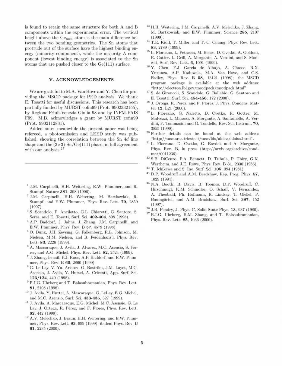
First we have measured the polar scans from the sur-face normal (normal emission, NE, conditions) to the
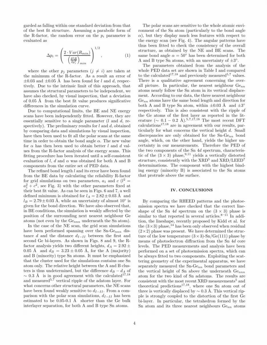
horizon (grazing emission) for six different photon ener-gies and the three inequivalent main symmetry directionsof the surface. The scans have been performed by keepingthe sample in transverse-magnetic (TM) polarization, i.e.with the scattering plane normal to the magnetic field ofthe photon beam, and rotating the analyzer in the scat-tering plane. When the surface is oriented with the [112]direction in the scattering plane, at a specific angle αfrom the surface normal the analyzer is aligned with theSn-Genn bond angle (see Fig. 3). In this, so called, bondemission (BE) geometry, the Sn photoelectrons can be ef-ficiently backscattered by the Genn atom and give rise tointensity maxima and minima, when changing the photonenergy. By a simple visual inspection, the bond directionα for both A and B Sn atoms can be roughly estimated as50◦ from the surface normal (see the polar scans taken at360 and 220 eV in Fig. 4). Given the information on thebond direction, the bond length l has been determinedby variable energy PED scans in BE geometry. The po-larization vector of the photon beam has been orientedat 50◦ from the surface normal, along the bond direction.This choice enhances the sensitivity to the Sn-Genn bondlength, as shown by MSCD simulations.15 A very simi-lar photon energy dependence has been found for both Aand B components in BE condition (see upper panel ofFig. 5).15 Finally, the Sn height d above the underneathGennn atom has been measured by taking energy scansin NE conditions and with the sample surface in TM po-larization. In this case the A and B components displaya remarkably different energy dependence, as can be seenin the lower panel of Fig. 5.
The quantitative evaluation of l, d and α for bothA and B type of Sn atoms has been performed by fit-ting the data to the MSCD simulations, starting fromthe geometric structure recently obtained by LDA-GCcalculations.17 The simulations have been performed ona 30 atom cluster centered on the Sn atom by consider-ing multiple scattering up to the 8th order, 4th Rehr-Albers order and with a pathcut of 1×10−4.16 Lowerpathcut values did not modify the simulations apprecia-bly. A Debye temperature of 230 K and an inner poten-tial V0 = 10 eV have been obtained by fitting the energyscans and successively they have been kept fixed in therecursive fitting procedure.
The fit quality has been evaluated by means of the
commonly used reliability factor R =
∑
(χexp−χcalc)2∑
(χ2exp+χ2
calc). In
order to compare our results with previously publishedstructural studies, the random error has been estimatedfollowing the approach of Woodruff and Bradshaw forthe analysis of the variable energy PED.25 By applyingthe method described by Pendry for LEED,26 the vari-ance of the R-factor is calculated for its minimum value.The variance is evaluated as V ar(Rmin) = Rmin
√
2/N ,where N is the number of independent pieces of struc-tural information within the spectrum energy range.25
All the parameter values pi yielding structures with as-sociated R-factor lower than Rmin + V ar(Rmin) are re-
3
garded as falling within one standard deviation from thatof the best fit structure. Assuming a parabolic form ofthe R-factor, the random error on the pi parameter isevaluated as
∆pi =
2 · V ar(Rmin)(
δ2Rδp2
i
)
min
1/2
, (1)
where the other pj parameters (j 6= i) are taken atthe minimum of the R-factor. As a result an error of±0.03 and ±0.05 A has been found for l and d, respec-tively. Due to the intrinsic limit of this approach, thatassumes the structural parameters to be independent, wehave also checked, by visual inspection, that a deviationof 0.05 A from the best fit value produces significativedifferences in the simulation curve.
Due to computational limits, the BE and NE energyscans have been independently fitted. However, they areessentially sensitive to a single parameter (l and d, re-spectively). The preliminary results for l and d, obtainedby comparing data and simulations by visual inspection,have then been used to fit all the polar scans at the sametime in order to obtain the bond angle α. The new valuefor α has then been used to obtain better l and d val-ues from the R-factor analysis of the energy scans. Thisfitting procedure has been iterated until a self-consistentevaluation of l, d and α was obtained for both A and Bcomponents from the entire set of PED data.
The refined bond length l and its error have been foundfrom the BE data by calculating the reliability R-factorfor grid simulations on two parameters, a1 and c (l2 =a21 + c2, see Fig. 3) with the other parameters fixed at
their best fit value. As can be seen in Figs. 6 and 7, a welldefined minimum is obtained for lA = 2.82± 0.03 A andlB = 2.79± 0.03 A, while an uncertainty of almost 10◦ isgiven for the bond direction. We have also observed that,in BE conditions, the simulation is weakly affected by theposition of the surrounding next nearest neighbour Geatoms (not even by the Gennn underneath the Sn atom).
In the case of the NE scan, the grid scan simulationshave been performed spanning over the Sn-Gennn dis-tance d and the distance dI−II between the first andsecond Ge bi-layers. As shown in Figs. 8 and 9, the R-factor analysis yields two different heights, dA = 2.92 ±0.05 A and dB = 3.23 ± 0.05 A, for the A (majority)and B (minority) type Sn atoms. It must be emphasizedthat the cluster used for the simulations contains one Snatom only. The relative height between the A and B clus-ters is thus undetermined, but the difference dB − dA of∼ 0.3 A is in good agreement with the calculated17,18
and measured5,7 vertical ripple of the adatom layer. Forwhat concerns other structural parameters, the NE scanshave been found weakly sensitive to dI−II . From a com-parison with the polar scan simulations, dI−II has beenestimated to be 0.05-0.1 A shorter than the Ge bulkinterlayer separation, for both A and B type Sn atoms.
The polar scans are sensitive to the whole atomic envi-ronment of the Sn atom (particularly to the bond angleα), but they display much less features with respect tothe energy scan (see Fig. 4). The angular patterns havethus been fitted to check the consistency of the overallstructure, as obtained by the NE and BE scans. Thesame bond angle α = 50◦ has been determined for bothA and B type Sn atoms, with an uncertainty of ±3◦.
The parameters obtained from the analysis of thewhole PED data set are shown in Table I and comparedto the calculated17,18 and previously measured5,7 values.There is a qualitative agreement concerning the over-all picture. In particular, the nearest neighbour Genn
atoms nearly follow the Sn atom in its vertical displace-ment. According to our data, the three nearest neighbourGenn atoms have the same bond length and direction forboth A and B type Sn atom, within ±0.03 A and ±3◦
respectively. This is also consistent with the ripple ofthe Ge atoms of the first layer as reported in the lit-erature (∼ 0.1 − 0.2 A).5,7,17,18 The most recent DFTcalculations17,18 are in agreement with our results, par-ticularly for what concerns the vertical height d. Smalldiscrepancies are only obtained for the Sn-Genn bondangle, which, on the other hand, yields the higher un-certainty in our measurements. Therefore the PED ofthe two components of the Sn 4d spectrum, characteris-tic of the (3 × 3) phase,9,11 yields a vertically distortedstructure, consistently with the XRD5 and XRD/LEED7
determinations. The component with the highest bind-ing energy (minority B) is associated to the Sn atomsthat protrude above the surface.
IV. CONCLUSIONS
By comparing the RHEED patterns and the photoe-mission spectra we have checked that the correct line-shape of the Sn 4d spectrum on the (3 × 3) phase issimilar to that reported in several articles.8–11 In addi-tion, the lineshape, recently proposed by Kidd et al. forthe (3×3) phase,14 has been only observed when residual(2×2) phase was present. We have determined the struc-ture of the low temperature (3×3)-Sn/Ge(111) phase bymeans of photoelectron diffraction from the Sn 4d corelevels. The PED measurements and analysis have beenperformed on a set of photoemission spectra, which canbe always fitted to two components. Exploiting the scat-tering geometry of the experimental apparatus, we haveseparately measured the Sn-Genn bond parameters andthe vertical height of Sn above the underneath Gennn
atom for the two kind of Sn adatoms. The results areconsistent with the most recent XRD measurements5 andtheoretical predictions17,18, where one Sn atom out ofthree is vertically displaced by ∼ 0.3 A. This vertical rip-ple is strongly coupled to the distortion of the first Gebi-layer. In particular, the tetrahedron formed by theSn atom and its three nearest neighbours Genn atoms
4
is found to retain the same structure for both A and Bcomponents within the experimental error. The verticalheight above the Gennn atom is the main difference be-tween the two bonding geometries. The Sn atoms thatprotrude out of the surface have the highest binding en-ergy (minority component), while the majority A com-ponent (lowest binding energy) is associated to the Snatoms that are pushed closer to the Ge(111) surface.
V. ACKNOWLEDGEMENTS
We are grateful to M.A. Van Hove and Y. Chen for pro-viding the MSCD package for PED analysis. We thankE. Tosatti for useful discussions. This research has beenpartially funded by MURST cofin99 (Prot. 9902332155),by Regione Friuli-Venezia Giulia 98 and by INFM-PAISF99. M.B. acknowledges a grant by MURST cofin99(Prot. 9902112831).
Added note: meanwhile the present paper was beingrefereed, a photoemission and LEED study was pub-lished, showing the correlation between the Sn 4d lineshape and the (3×3)-Sn/Ge(111) phase, in full agreementwith our analysis.27
1 J.M. Carpinelli, H.H. Weitering, E.W. Plummer, and R.Stumpf, Nature 381, 398 (1996).
2 J.M. Carpinelli, H.H. Weitering, M. Bartkowiak, R.Stumpf, and E.W. Plummer, Phys. Rev. Lett. 79, 2859(1997).
3 S. Scandolo, F. Ancilotto, G.L. Chiarotti, G. Santoro, S.Serra, and E. Tosatti, Surf. Sci. 402-404, 808 (1998).
4 A.P. Baddorf, J. Jahns, J. Zhang, J.M. Carpinelli, andE.W. Plummer, Phys. Rev. B 57, 4579 (1998).
5 O. Bunk, J.H. Zeysing, G. Falkenberg, R.L. Johnson, M.Nielsen, M.M. Nielsen, and R. Feidenhans’l, Phys. Rev.Lett. 83, 2226 (1999).
6 A. Mascaraque, J. Avila, J. Alvarez, M.C. Asensio, S. Fer-rer, and A.G. Michel, Phys. Rev. Lett. 82, 2524 (1999).
7 J. Zhang, Ismail, P.J. Rous, A.P. Baddorf, and E.W. Plum-mer, Phys. Rev. B 60, 2860 (1999).
8 G. Le Lay, V. Yu. Aristov, O. Bostrom, J.M. Layet, M.C.Asensio, J. Avila, Y. Huttel, A. Cricenti, App. Surf. Sci.123/124, 440 (1998).
9 R.I.G. Uhrberg and T. Balasubramanian, Phys. Rev. Lett.81, 2108 (1998).
10 J. Avila, Y. Huttel, A. Mascaraque, G. LeLay, E.G. Michel,and M.C. Asensio, Surf. Sci. 433-435, 327 (1999).
11 J. Avila, A. Mascaraque, E.G. Michel, M.C. Asensio, G. LeLay, J. Ortega, R. Perez, and F. Flores, Phys. Rev. Lett.82, 442 (1999).
12 A.V. Melechko, J. Braun, H.H. Weitering, and E.W. Plum-mer, Phys. Rev. Lett. 83, 999 (1999); ibidem Phys. Rev. B61, 2235 (2000).
13 H.H. Weitering, J.M. Carpinelli, A.V. Melechko, J. Zhang,M. Bartkowiak, and E.W. Plummer, Science 285, 2107(1999).
14 T.E. Kidd, T. Miller, and T.-C. Chiang, Phys. Rev. Lett.83, 2789 (1999).
15 L. Floreano, L. Petaccia, M. Benes, D. Cvetko, A. Goldoni,R. Gotter. L. Grill, A. Morgante, A. Verdini, and S. Mod-esti, Surf. Rev. Lett. 6, 1091 (1999).
16 Y. Chen, F.J. Garcia de Albajo, A. Chasse, R.X.Ynzunza, A.P. Kaduwela, M.A. Van Hove, and C.S.Fadley, Phys. Rev. B 58, 13121 (1998); the MSCDprogram package is available at the web address:“http://electron.lbl.gov/mscdpack/mscdpack.html”.
17 S. de Gironcoli, S. Scandolo, G. Ballabio, G. Santoro andE. Tosatti, Surf. Sci. 454-456, 172 (2000).
18 J. Ortega, R. Perez, and F. Flores, J. Phys. Condens. Mat-ter 12, L21 (2000).
19 L. Floreano, G. Naletto, D. Cvetko, R. Gotter, M.Malvezzi, L. Marassi, A. Morgante, A. Santaniello, A. Ver-dini, F. Tommasini and G. Tondello, Rev. Sci. Instrum. 70,3855 (1999).
20 Further details can be found at the web address“http://tasc.area.trieste.it/tasc/lds/aloisa/aloisa.html”.
21 L. Floreano, D. Cvetko, G. Bavdek and A. Morgante,Phys. Rev. B, in press (http://arxiv.org/archive/cond-mat/0011236).
22 S.B. DiCenzo, P.A. Bennett, D. Tribula, P. Thiry, G.K.Wertheim, and J.E. Rowe, Phys. Rev. B 31, 2330 (1985).
23 T. Ichikawa and S. Ino, Surf. Sci. 105, 394 (1981).24 D.P. Woodruff and A.M. Bradshaw, Rep. Prog. Phys. 57,
1029 (1994).25 N.A. Booth, R. Davis, R. Toomes, D.P. Woodruff, C.
Hirschmugl, K.M. Schindler, O. Schaff, V. Fernandez,A. Theobald, Ph. Hofmann, R. Lindsay, T. Gießel, P.Baumgartel, and A.M. Bradshaw, Surf. Sci. 387, 152(1997).
26 J.B. Pendry, J. Phys. C, Solid State Phys. 13, 937 (1980).27 R.I.G. Uhrberg, H.M. Zhang, and T. Balasubramanian,
Phys. Rev. Lett. 85, 1036 (2000).
5

Parameter SXRD5 SXRD/LEED7 LDA-LO18 LDA-GC17 Present paper
αA 50◦ 51.5◦ 51.8◦ 51.2◦ 50◦
αB 47.4◦ 46.9◦ 49◦ 47◦ 50◦
lA(A) 2.80 2.89 2.78 2.79 2.82lB(A) 2.88 2.93 2.79 2.84 2.79dA(A) 3.03 2.97 2.90 2.92 2.92dB(A) 3.32 3.34 3.13 3.25 3.23
dI−II(A) 2.36-2.39 2.39 2.31-2.36 2.34-2.39 2.34-2.40∆Sn(A) 0.29 0.37 0.23 0.33 0.31
TABLE I. The best fit values for the parameters α, l, d and dI−II , compared to recent experimental measurements andtheoretical calculations. The calculated random errors are ∆l = 0.03 A, ∆d = 0.05 A, ∆dI−II = 0.12 A, and ∆α = 3◦ for bothA and B components. The vertical ripple ∆Sn has been simply evaluated as dB − dA. The geometric parameters reported forthe majority A component from Ref. [5] represent the mean value of the two lower height Sn atoms (whose coordinates wereseparately determined).
6
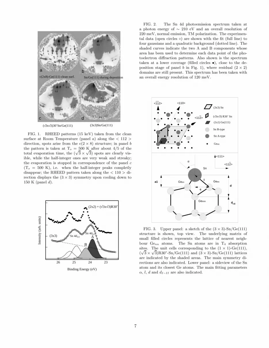
0,0
1,0 -1,11,0 -1,1
0,0
-2,1-2,1
0,0
-2,1
1,0 -1,11,1 0,1
-1,1
0,1/3
1,1/3 -1,1/3
a b
c d
c(2x8)-Ge(111) clean surf. Sn/Ge(111) during deposition
(√3x√3)30˚Sn/Ge(111) (3x3)Sn/Ge(111)
FIG. 1. RHEED patterns (15 keV) taken from the cleansurface at Room Temperature (panel a) along the < 112 >
direction, spots arise from the c(2 × 8) structure; in panel b
the pattern is taken at Ts = 500 K after about 4/5 of thetotal evaporation time, the (
√3 ×
√3) spots are clearly vis-
ible, while the half-integer ones are very weak and streaky;the evaporation is stopped in correspondence of the panel c
(Ts = 500 K), i.e. when the half-integer peaks completlydisappear; the RHEED pattern taken along the < 110 > di-rection displays the (3 × 3) symmetry upon cooling down to150 K (panel d).
Inte
nsity
(ar
b. u
nits
)
26 25 24 23
Binding Energy (eV)
Sn 4d3/2
Sn 4d5/2
(2x2) + (√3x√3)R30˚
(3x3) A
B
FIG. 2. The Sn 4d photoemission spectrum taken ata photon energy of ∼ 210 eV and an overall resolution of220 meV, normal emission, TM polarization. The experimen-tal data (open circles ◦) are shown with the fit (full line) tofour gaussians and a quadratic background (dotted line). Theshaded curves indicate the two A and B components whosearea has been used to determine each data point of the pho-toelectron diffraction patterns. Also shown is the spectrumtaken at a lower coverage (filled circles •), close to the de-position stage of panel b in Fig. 1), where residual (2 × 2)domains are still present. This spectrum has been taken withan overall energy resolution of 120 meV.
<110>
(3x3) Sn
(√3x√3) R30˚ Sn
Sn B-type
Sn A-type
Genn
(1x1) Ge(111)
da1
l
α
Sn
Gennn
c
Genn
dI-II
<111>
Genn
<112>
<112>
<112>
__
_
_
FIG. 3. Upper panel: a sketch of the (3 × 3)-Sn/Ge(111)structure is shown, top view. The underlying matrix ofsmall filled circles represents the lattice of nearest neigh-bour Genn atoms. The Sn atoms are in T4 absorptionsites. The unit cells corresponding to the (1 × 1)-Ge(111),(√
3 ×√
3)R30◦-Sn/Ge(111) and (3 × 3)-Sn/Ge(111) latticesare indicated by the shaded areas. The main symmetry di-rections are also indicated. Lower panel: a sideview of the Snatom and its closest Ge atoms. The main fitting parametersα, l, d and dI−II are also indicated.
7

hν = 260 eV
A
B
0.2
0.0
-0.2
χ
hν = 360 eV
A
B
0.2
0.0
-0.2
χ
6040200
Polar Angle (Deg)
hν = 244 eV
A
B
α 6040200
Polar Angle (Deg)
hν = 220 eV
A
B
α
FIG. 4. Photoelectron diffraction polar scans taken alongthe [112] direction at four different photon energies: 220, 244,260 and 360 eV. The emission angle is measured from thesurface normal (0◦). An offset of 0.2 has been added to theA χ-function for the sake of clarity. At 50-52◦, the scansdisplay a maximum (220 and 360 eV) or a minimum (244and 260 eV) depending on the interference conditions of theprimary photoelectron wave with that backscattered by thenearest neighbour Ge atoms. The best fit simulations arealso shown (full lines). The vertical dashed lines indicate theSn-Genn bond angle α from the surface normal.
-0.3
-0.2
-0.1
0.0
0.1
0.2
0.3
χ
1110987
k (Å-1)
BE geometry A B
-0.3
-0.2
-0.1
0.0
0.1
0.2
0.3
χ
10987
k (Å-1)
NE geometry
A B
FIG. 5. Upper panel: χ-function of the energy scan inbond emission geometry for the A and B components (filledand open circles, respectively). This PED measurement ismainly sensitive to the Sn-Genn bond length l. Lower panel:χ-function of the energy scan in normal emission geometryfor the A and B components (filled and open circles, respec-tively). This PED measurement is mainly sensitive to theSn vertical height d above the Gennn atom underneath. Notethat the data presented here are based on a more extended setof spectra with respect to our previous study,15 thus yieldinga better statistics and, in the case of normal emission data, amore extended energy range too.
8

1.90
1.85
1.80
1.75
1.70
1.65
a 1 (
Å)
2.302.252.202.152.10c (Å)
1.6
1.6
1.2
1.2
0.8
0.8
0.6
0.6
0.4
0.4
2.86
2.82
2.78
49˚
50˚
51˚
52˚
53˚
0.4
0.35
0.351.2
1.0
0.8
0.6
0.4
0.2
R
2.952.902.852.802.752.70
lA (Å)
∆lA
Var(Rmin)
αA= 50˚
-0.2
-0.1
0.0
0.1
0.2
χ
1110987
k (Å-1)
A component; BE geometry
FIG. 6. Bond length analysis of the main component in bond emission (BE) geometry. Both the photon polarizationvector and the electron analyzer have been oriented at 50◦ from the surface normal, along the Sn-Genn bond direction. Leftupper panel: kinetic momentum (wavenumber) dependence of the χ-function for the A (majority) component of the Sn 4d
photoelectrons in bond emission. The best fit (full line) is overimposed to the experimental data (filled circles •). Right panel:contour plot of the MSCD simulation R-factor for the a1 and c parameters (see Fig. 3). The bond length lA (dashed thick lineswith markers on white background) and the bond angle αA (full thick lines with markers on gray background) are reported fora few values. Left bottom panel: statistical analysis of the random error for the parameter lA with the other parameters attheir best fit value, as reported in Table 1. The R-factor values (filled squares) have been fitted to a parabolic curve (full line).The R-factor variance and the corresponding error on the parameter are also reported.
2.0
1.9
1.8
1.7
1.6
a 1 (
Å)
2.42.32.22.12.0 c (Å)
1.65
1.45
0.85
0.65
0.65
0.45
0.45
0.25
50˚
54°
48°
52°
2.85
2.79
2.73
0.25
1.05
1.05
1.65
0.85
1.45
-0.3
-0.2
-0.1
0.0
0.1
0.2
0.3
χ
1110987
k (Å-1)
B component, BE geometry
1.2
1.0
0.8
0.6
0.4
0.2
R
2.902.852.802.752.70
lB (Å)
αB= 50˚
Var(Rmin)
∆lB
FIG. 7. Bond length analysis of the secondary component in BE geometry. The labeling is the same of Fig. 6.
9
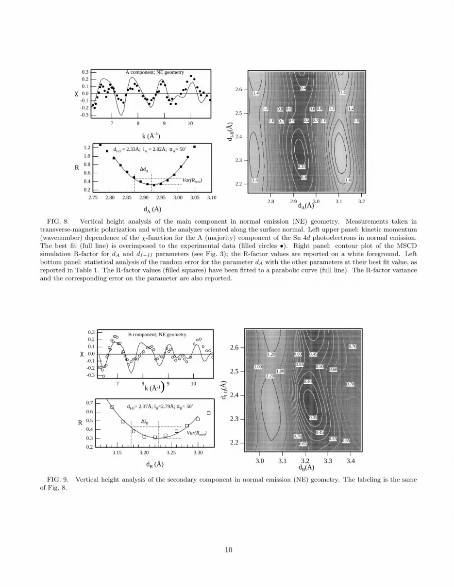
1.2
1.0
0.8
0.6
0.4
0.2
R
3.103.053.002.952.902.852.802.75
dA (Å)
dI-II = 2.33Å; lA = 2.82Å; αA= 50˚
Var(Rmin)
∆dA
2.6
2.5
2.4
2.3
2.2
d I-I
I(Å
)
3.23.13.02.92.8dA(Å)
0.4
0.5
0.6
0.7
0.8
0.4
0.8
1.01.0
1.21.2 1.2
1.4
1.41.4
1.4
0.5
0.6
0.7 1.0
0.35
-0.3-0.2-0.10.00.10.20.3
χ
10987
k (Å-1)
A component; NE geometry
FIG. 8. Vertical height analysis of the main component in normal emission (NE) geometry. Measurements taken intransverse-magnetic polarization and with the analyzer oriented along the surface normal. Left upper panel: kinetic momentum(wavenumber) dependence of the χ-function for the A (majority) component of the Sn 4d photoelectrons in normal emission.The best fit (full line) is overimposed to the experimental data (filled circles •). Right panel: contour plot of the MSCDsimulation R-factor for dA and dI−II parameters (see Fig. 3); the R-factor values are reported on a white foreground. Leftbottom panel: statistical analysis of the random error for the parameter dA with the other parameters at their best fit value, asreported in Table 1. The R-factor values (filled squares) have been fitted to a parabolic curve (full line). The R-factor varianceand the corresponding error on the parameter are also reported.
2.6
2.5
2.4
2.3
2.2
d I-I
I(Å
)
3.43.33.23.13.0dB(Å)
0.40
0.500.60
1.001.00
0.45
0.45
0.35
0.60
0.70
0.70
0.70
1.20
1.20
0.55 0.65
0.55
0.65
-0.3-0.2-0.10.00.10.20.3
χ
10987k (Å-1)
B component; NE geometry
0.7
0.6
0.5
0.4
0.3
0.2
R
3.303.253.203.15
dB (Å)
∆lB
Var(Rmin)
dI-II = 2.37Å; lB=2.79Å; αB= 50˚
FIG. 9. Vertical height analysis of the secondary component in normal emission (NE) geometry. The labeling is the sameof Fig. 8.
10


