Embed Size (px)
Citation preview
Progress In Electromagnetics Research, Vol. 106, 91–106, 2010
DESIGN OF CMOS QUADRATURE VCO USING ON-CHIP TRANS-DIRECTIONAL COUPLERS
C.-I. Shie, J.-C. Cheng, S.-C. Chou, and Y.-C. Chiang
Department of Electronic EngineeringChang Gung UniversityNo. 259 Wen-Hwa 1st Road, Kwei-ShanTao-Yuan 333, Taiwan, R.O.C.
Abstract—This work presents a quadrature voltage-controlledoscillator (QVCO) realized by on-chip trans-directional (TRD)couplers. The TRD coupler is implemented by sections of parallel-coupled lines connected by shunt capacitors periodically. TheTRD couplers allow decoupling the DC path between input andoutput. Thus, it can make connections with active circuits easier,eliminating some off-chip biasing circuits. Since the quadrature signalsare generated by 90 hybrid couplers, the oscillator core can beoptimized for circuit performance without considering the generationof quadrature signals. A Ka band QVCO fabricated in CMOS 0.18µmtechnology was designed to verify the effectiveness of the proposedQVCO structure. The measurement results reveal that the quadratureoutput signals of QVCO have about −1.52 dBm output powers withless than 1 dB amplitude imbalance and less than 6 phase differencein the frequency range of 31.9 to 32.7 GHz. The best measured phasenoise of the QVCO is −110.6 dBc/Hz at 1 MHz offset from the centerfrequency. The figure-of-merit of the circuit is 187.5 dBc/Hz.
1. INTRODUCTION
QVCO is a widely used component in modern digital communicationsystems. Wireless transceivers usually adopt the quadrature localoscillation signaling scheme to reject unwanted image signals duringthe up- or down-conversion of the communication signals. In publishedpapers, the most commonly used structure is the one using two
Received 30 May 2010, Accepted 8 July 2010, Scheduled 12 July 2010Corresponding author: C.-I. Shie ([email protected]).
92 Shie et al.
pairs of cross-coupled VCOs connected by parallel or series couplingtransistors [1–4]. However, such a structure is difficult to operate above20GHz because of the device delay of the cross-coupling transistorsand the parasitic effect of the interconnections inside the circuits [5–8]. Another disadvantage of this structure is that a compromise mustbe made among quadrature accuracy, power consumption and phasenoise. Therefore, a rotary traveling-wave topology is proposed to formthe multiphase VCO [9] in which phase delay lines are used, limiting itsoperation bandwidth. Besides, lots of CMOS VCOs or QVCOs adoptopen drain buffers as output stages, leaving the separation of DC andRF path to off-chip circuits such as bias-Ts [10–12]. For a single chipsolution, adding on-chip DC blocking circuits will enlarge chip sizesand deteriorate the output signals.
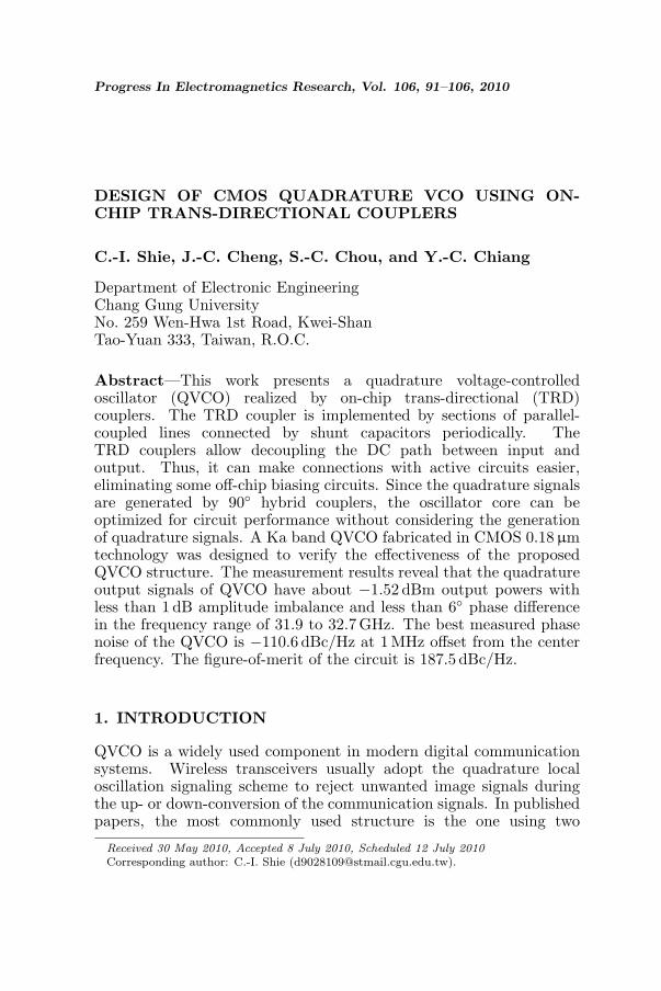
In [13], a novel TRD coupler implemented by parallel coupledmicrostrip lines is proposed as shown in Fig. 1. This coupler isconstructed by sections of coupled lines with shunt capacitors placedperiodically between them. Unlike codirectional and contradirectionalcouplers [14–16], the through and coupled ports of this TRD couplerare on the same microstrip line. Thus, it has the benefit of DCisolation between input and output ports. And it does not use thecomposite right/left handed structure [17–20]. When connected toactive circuits, it is possible to utilize this feature to save DC blockingcircuits. In [13], quadrature hybrids based on the TRD coupler havebeen designed and fabricated. Good quadrature phase difference andamplitude balance between the two output ports over a 26% bandwidthhave been achieved in this work.
Input Isolation
ThroughCoupled
1 2
34
Figure 1. Topology of the proposed TRD coupler.
In this paper, we propose a novel QVCO in which two quadraturehybrids implemented by TRD couplers are connected to the outputports of a cross-coupled VCO to generate quadrature signals. Sincethe required quadrature phase and equal amplitude of the quadraturesignals mainly depend on the performance of the quadrature hybrids,the cross-coupled VCO can be optimized to achieve lowest phase noiseor maximum output power. Due to the TRD couplers, circuits for DCand RF separation can also be avoided.
To verify the characteristics of the proposed QVCO, a Ka-bandprototype was designed and fabricated in CMOS 0.18-µm technology.The measured results show that the output power at each port reaches
Progress In Electromagnetics Research, Vol. 106, 2010 93
−1.52 dBm in the frequency range of 31.9 to 32.7 GHz. The bestmeasured phase noise is −110.6 dBc/Hz at 1 MHz offset frequencyof the carrier frequency. The figure-of-merit (FOM) is 187.5 dBc/Hzwhich is considered high for a Ka-band QVCO.
In the following section, the analysis and design of the proposedquadrature hybrids based on the TRD couplers is presented. InSection 3, the proposed QVCO is designed and fabricated. Finally,conclusions are given in Section 4.
2. DESIGNS AND IMPLEMENT OF THE TRDCOUPLER
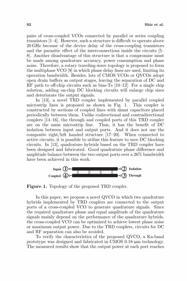
A TRD CPW coupler as shown in Fig. 2(a) is consisted of identicalsections of parallel coupled CPWs and shunt capacitors implementedby floating plates. The floating plate in each cell creates extracapacitances among itself, the coupled lines and the ground. Theequivalent circuits are shown in Fig. 2(b). To increase the capacitancebetween the floating plates and the coupled lines, the CTM5 layer isadded between the two metal layers to reduce the effective distancebetween them [21] (Fig. 2(c)).
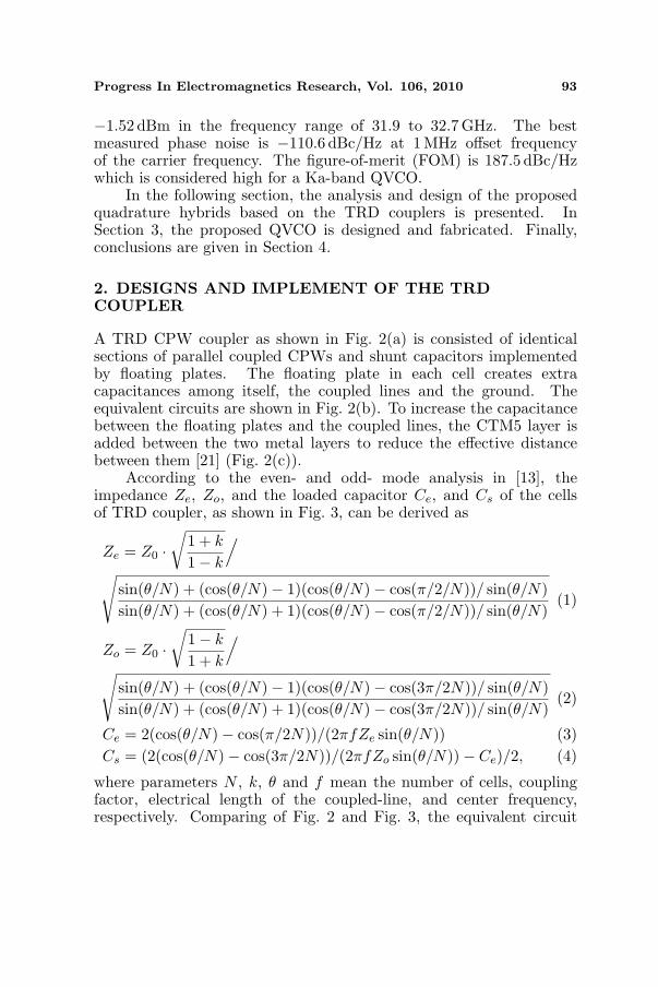
According to the even- and odd- mode analysis in [13], theimpedance Ze, Zo, and the loaded capacitor Ce, and Cs of the cellsof TRD coupler, as shown in Fig. 3, can be derived as
Ze = Z0 ·√
1 + k
1− k
/
√sin(θ/N) + (cos(θ/N)− 1)(cos(θ/N)− cos(π/2/N))/ sin(θ/N)sin(θ/N) + (cos(θ/N) + 1)(cos(θ/N)− cos(π/2/N))/ sin(θ/N)
(1)
Zo = Z0 ·√
1− k
1 + k
/
√sin(θ/N) + (cos(θ/N)− 1)(cos(θ/N)− cos(3π/2N))/ sin(θ/N)sin(θ/N) + (cos(θ/N) + 1)(cos(θ/N)− cos(3π/2N))/ sin(θ/N)
(2)
Ce = 2(cos(θ/N)− cos(π/2N))/(2πfZe sin(θ/N)) (3)Cs = (2(cos(θ/N)− cos(3π/2N))/(2πfZo sin(θ/N))− Ce)/2, (4)
where parameters N , k, θ and f mean the number of cells, couplingfactor, electrical length of the coupled-line, and center frequency,respectively. Comparing of Fig. 2 and Fig. 3, the equivalent circuit
94 Shie et al.
gap
wid
th
length
CPW
Coupled
Lines
Floating
Plates
Ground
spac
e5
0µm
A
A
50 µ
m
(a)
Ground Ground
Cfl
Cfg Cfg
Cfl
CPW Coupled Line
(b)
(c)
Ground
M5
M6
CTM5
M6Ground
(CPW)(CPW)
(Floating plate)
Figure 2. (a) Topology of TRD coupler in the integrated technology.(b) The equivalent capacitance network of AA cross section. (c) Layoutof AA cross section.
sC2
eC
N2/θ N2/θ
eZ
oZ s
C2
eC
Figure 3. Equivalent circuit of periodical loaded coupled-line cell ofTRD coupler.
parameters of the floating plate can be related as follows
Ce =1
1/Cfg + 1/Cfl(5)
Cs = Cfl/2 (6)
Progress In Electromagnetics Research, Vol. 106, 2010 95
Table 1. Parameters of the TRD coupler.
TRD Coupler Parameters values
Center Frequency (GHz) 30
Space (µm) 23
Width (µm) 21
Gap (µm) 12
Length (µm) 880
Number of Cells N 4
θ 66
k −3 dB
Ze ( Ω ) 89.4
Zo ( Ω ) 51.5
Cs ( fF ) 201.5
Ce ( fF ) 14.6
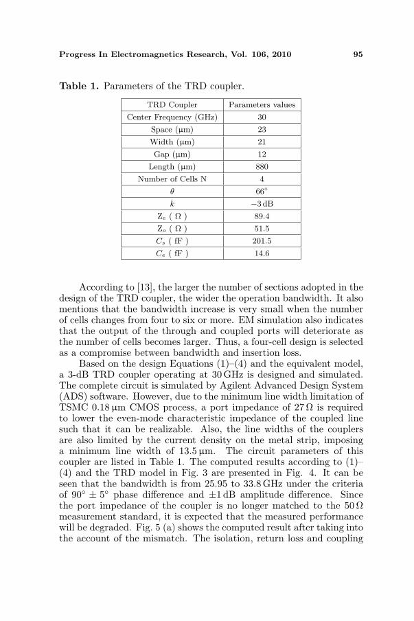
According to [13], the larger the number of sections adopted in thedesign of the TRD coupler, the wider the operation bandwidth. It alsomentions that the bandwidth increase is very small when the numberof cells changes from four to six or more. EM simulation also indicatesthat the output of the through and coupled ports will deteriorate asthe number of cells becomes larger. Thus, a four-cell design is selectedas a compromise between bandwidth and insertion loss.
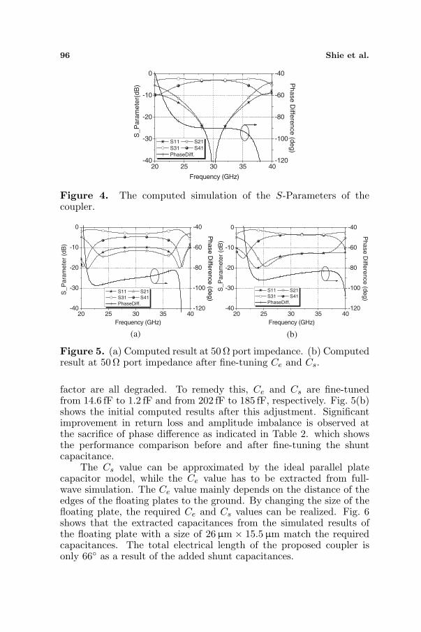
Based on the design Equations (1)–(4) and the equivalent model,a 3-dB TRD coupler operating at 30 GHz is designed and simulated.The complete circuit is simulated by Agilent Advanced Design System(ADS) software. However, due to the minimum line width limitation ofTSMC 0.18µm CMOS process, a port impedance of 27 Ω is requiredto lower the even-mode characteristic impedance of the coupled linesuch that it can be realizable. Also, the line widths of the couplersare also limited by the current density on the metal strip, imposinga minimum line width of 13.5µm. The circuit parameters of thiscoupler are listed in Table 1. The computed results according to (1)–(4) and the TRD model in Fig. 3 are presented in Fig. 4. It can beseen that the bandwidth is from 25.95 to 33.8 GHz under the criteriaof 90 ± 5 phase difference and ±1 dB amplitude difference. Sincethe port impedance of the coupler is no longer matched to the 50 Ωmeasurement standard, it is expected that the measured performancewill be degraded. Fig. 5 (a) shows the computed result after taking intothe account of the mismatch. The isolation, return loss and coupling
96 Shie et al.
20 25 30 35 40-40
-30
-20
-10
0
S11 S21
S31 S41
PhaseDiff.
-120
-100
-80
-60
-40
Frequency (GHz)
S_
Pa
ram
ete
r(d
B)
Ph
ase
Diffe
ren
ce
(de
g)
Figure 4. The computed simulation of the S-Parameters of thecoupler.
20 25 30 35 40-40
-30
-20
-10
0
S11 S21
S31 S41
PhaseDiff.-120
-100
-80
-60
-40
Frequency (GHz)
S_
Pa
ram
ete
r (d
B)
Ph
ase
Diffe
ren
ce
(de
g)
20 25 30 35 40-40
-30
-20
-10
0
S11 S21
S31 S41
PhaseDiff.
-120
-100
-80
-60
-40S
_P
ara
me
ter
(dB
)
Ph
ase
Diffe
ren
ce
(de
g)
Frequency (GHz)
(a) (b)
Figure 5. (a) Computed result at 50 Ω port impedance. (b) Computedresult at 50Ω port impedance after fine-tuning Ce and Cs.
factor are all degraded. To remedy this, Ce and Cs are fine-tunedfrom 14.6 fF to 1.2 fF and from 202 fF to 185 fF, respectively. Fig. 5(b)shows the initial computed results after this adjustment. Significantimprovement in return loss and amplitude imbalance is observed atthe sacrifice of phase difference as indicated in Table 2. which showsthe performance comparison before and after fine-tuning the shuntcapacitance.
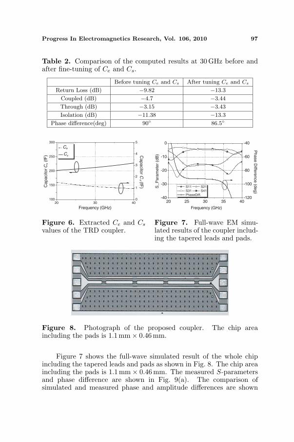
The Cs value can be approximated by the ideal parallel platecapacitor model, while the Ce value has to be extracted from full-wave simulation. The Ce value mainly depends on the distance of theedges of the floating plates to the ground. By changing the size of thefloating plate, the required Ce and Cs values can be realized. Fig. 6shows that the extracted capacitances from the simulated results ofthe floating plate with a size of 26µm × 15.5µm match the requiredcapacitances. The total electrical length of the proposed coupler isonly 66 as a result of the added shunt capacitances.
Progress In Electromagnetics Research, Vol. 106, 2010 97
Table 2. Comparison of the computed results at 30 GHz before andafter fine-tuning of Ce and Cs.
Before tuning Ce and Cs After tuning Ce and Cs
Return Loss (dB) −9.82 −13.3
Coupled (dB) −4.7 −3.44
Through (dB) −3.15 −3.43
Isolation (dB) −11.38 −13.3
Phase difference(deg) 90 86.5
20 30 40100
150
200
250
300
Ce
Cs
Frequency (GHz)
Ca
pa
cito
r C
s (
fF)
0
1
2
3
4
5
Ca
pa
cito
r Ce (fF
)
Figure 6. Extracted Ce and Cs
values of the TRD coupler.
20 25 30 35 40-40
-30
-20
-10
0
S11 S21
S31 S41
PhaseDiff.-120
-100
-80
-60
-40
Frequency (GHz)
S_
Pa
ram
ete
r (d
B)
Ph
ase
Diffe
ren
ce
(de
g)
Figure 7. Full-wave EM simu-lated results of the coupler includ-ing the tapered leads and pads.
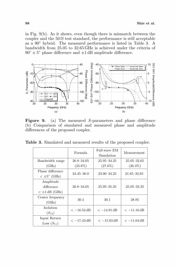
Figure 8. Photograph of the proposed coupler. The chip areaincluding the pads is 1.1 mm× 0.46 mm.
Figure 7 shows the full-wave simulated result of the whole chipincluding the tapered leads and pads as shown in Fig. 8. The chip areaincluding the pads is 1.1mm× 0.46 mm. The measured S-parametersand phase difference are shown in Fig. 9(a). The comparison ofsimulated and measured phase and amplitude differences are shown
98 Shie et al.
in Fig. 9(b). As it shows, even though there is mismatch between thecoupler and the 50 Ω test standard, the performance is still acceptableas a 90 hybrid. The measured performance is listed in Table 3. Abandwidth from 25.05 to 32.65 GHz is achieved under the criteria of90 ± 5 phase difference and ±1 dB amplitude difference.
20 25 30 35 40-40
-30
-20
-10
0
S11 S21
S31 S41
PhaseDiff.-120
-100
-80
-60
-40
Frequency (GHz)
S_
Pa
ram
ete
r (d
B)
Ph
ase
Diffe
ren
ce
(de
g)
20 25 30 35 40-120
-100
-80
-60
-40 Phase Meas. Ampl itude Meas.
Phase Simu. Ampl itude Simu.
S31-S
41 P
hase D
iffe
rence (
deg)
-10
-5
0
5
10
S3
1-S
41
Am
plitu
de
Diffe
ren
ce
(dB
)
Frequency (GHz)
(a) (b)
Figure 9. (a) The measured S-parameters and phase difference(b) Comparison of simulated and measured phase and amplitudedifferences of the proposed coupler.
Table 3. Simulated and measured results of the proposed coupler.
FormulaFull-wave EM
SimulationMeasurement
Bandwidth range
(GHz)
26.8–34.05
(23.8%)
25.95–34.25
(27.6%)
25.05–32.65
(26.3%)
Phase difference
< ±5 (GHz)24.45–36.0 23.00–34.25 21.65–32.65
Amplitude
difference
< ±1 dB (GHz)
26.8–34.05 25.95–35.35 25.05–33.35
Center frequency
(GHz)30.4 30.1 28.85
Isolation
(S12)< −16.52 dB < −14.91 dB < −11.16 dB
Input Return
Loss (S11)< −17.43 dB < −15.03 dB < −11.64 dB
Progress In Electromagnetics Research, Vol. 106, 2010 99
3. DESIGNS AND IMPLEMENT OF THE QVCOCIRCUIT
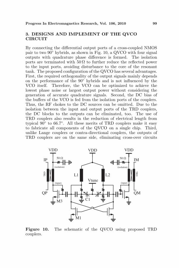
By connecting the differential output ports of a cross-coupled NMOSpair to two 90 hybrids, as shown in Fig. 10, a QVCO with four signaloutputs with quadrature phase difference is formed. The isolationports are terminated with 50 Ω to further reduce the reflected powerto the input ports, avoiding disturbance to the core of the resonanttank. The proposed configuration of the QVCO has several advantages.First, the required orthogonality of the output signals mainly dependson the performance of the 90 hybrids and is not influenced by theVCO itself. Therefore, the VCO can be optimized to achieve thelowest phase noise or largest output power without considering thegeneration of accurate quadrature signals. Second, the DC bias ofthe buffers of the VCO is fed from the isolation ports of the couplers.Thus, the RF chokes to the DC sources can be omitted. Due to theisolation between the input and output ports of the TRD couplers,the DC blocks to the outputs can be eliminated, too. The use ofTRD couplers also results in the reduction of electrical length fromtypical 90 to 66.7. All these merits of TRD couplers make it easyto fabricate all components of the QVCO on a single chip. Third,unlike Lange couplers or contra-directional couplers, the outputs ofTRD couplers are on the same side, eliminating cross-over circuits
VDD VDD
Vtune
IP
QP
IM
QM
VDD
(input)
TR
D
50 Ω 50 Ω
TR
D
(isolation)
(input)
(isolation)
M1
M3 C1
L1 L2
Figure 10. The schematic of the QVCO using proposed TRDcouplers.
100 Shie et al.
which add unpredictable losses and phase delays. Fourth, the proposedQVCO uses only two buffers comparing to four in traditional QVCOswhich require one on each quadrature output path. Thus, the circuit issimpler and power consumption of the output buffers is reduced. Notethat by setting the gate bias of the transistors in the output buffersto the supply voltage (VDD), stable operation against VDD variationand the required operating region can be achieved with a simple circuitconfiguration [22]. The main drawback of the proposed QVCO is thelarger chip area to form the TRD couplers. However, its size can bereduced further by using meander-like and stacked transmission-linesto form the TRD couplers. And it may be more convenient to combinewith the other circuit such as mixer.
To reach the start-up condition for oscillation at as high as30GHz in 0.18µm technology, an NMOS cross-coupled pair is adoptedto decrease the parasitic capacitance in the transistors. At thesame transconductance, PMOS transistors exhibit more parasiticcapacitance, lowering the oscillation frequency of the resonant tank.The NMOS M1 of the core circuit is composed of 18 fingers with aspectratio 1.84µm/0.18µm (width/length). The NMOS M3 of the buffercircuit is composed of 64 fingers with aspect ratio 1.5µm/0.18µm(width/length). The accumulated-mode MOS varactor C1 is formedby N-type diffusion and the thick oxide [21]. The thick oxide MOSvaractor has a lower tuning sensitivity and a higher quality factor thanthe normal thin oxide varactor because it can decrease the electric fieldin the oxide. Thus, it can achieve a good phase noise when used to forma resonance tank. The MOS varactor is composed of 10 branch, andeach branch is 0.5µm × 2.5µm in size. A center-taped inductor is usedto implement L1 and L2 to minimize the chip area and to maximizethe quality factor. By properly forming the inductor, the maximumquality factor of the inductor can be located at close to the operatingfrequency to improve the circuit performance. The simulated resultsreveal that the output power of the QVCO is greater than −1 dBmwith a phase noise of −107 dBc/Hz at 1MHz offset from the carrierfrequency 30 GHz.
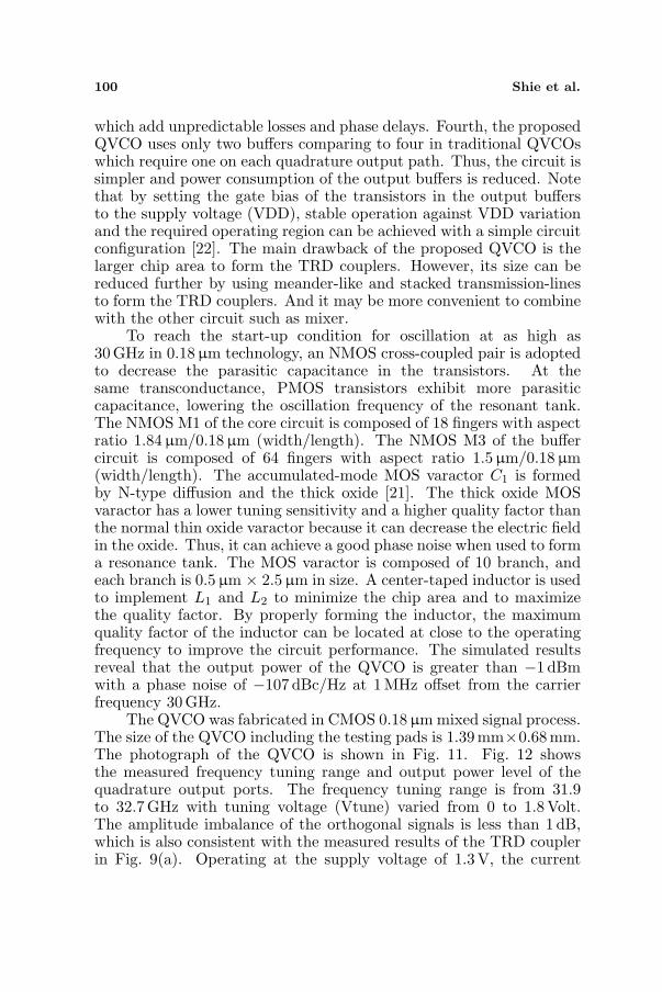
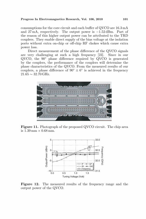
The QVCO was fabricated in CMOS 0.18µm mixed signal process.The size of the QVCO including the testing pads is 1.39 mm×0.68mm.The photograph of the QVCO is shown in Fig. 11. Fig. 12 showsthe measured frequency tuning range and output power level of thequadrature output ports. The frequency tuning range is from 31.9to 32.7GHz with tuning voltage (Vtune) varied from 0 to 1.8 Volt.The amplitude imbalance of the orthogonal signals is less than 1 dB,which is also consistent with the measured results of the TRD couplerin Fig. 9(a). Operating at the supply voltage of 1.3 V, the current
Progress In Electromagnetics Research, Vol. 106, 2010 101
consumptions for the core circuit and each buffer of QVCO are 16.3 mAand 27mA, respectively. The output power is −1.52 dBm. Part ofthe reason of this higher output power can be attributed to the TRDcouplers. They enable direct supply of the bias voltage at the isolationports without extra on-chip or off-chip RF chokes which cause extrapower loss.
Direct measurement of the phase difference of the QVCO signalsare very challenging at such a high frequency [23]. Since in ourQVCO, the 90 phase difference required by QVCO is generatedby the couplers, the performance of the couplers will determine thephase characteristics of the QVCO. From the measured results of ourcouplers, a phase difference of 90 ± 6 is achieved in the frequency21.65 ∼ 32.70 GHz.
Figure 11. Photograph of the proposed QVCO circuit. The chip areais 1.39 mm× 0.68mm.
0.0 0.5 1.0 1.5-10
-5
0
5
IP QP
IM QM
Frequency
Tuning Voltage (Volt)
Outp
utP
ow
er
(dB
m)
31.5
32.0
32.5
33.0
Fre
quency (G
Hz)
Figure 12. The measured results of the frequency range and theoutput power of the QVCO.
102 Shie et al.
Figure 13. Measured result of the phase noise of QVCO v. s. offsetfrequency at zero tuning voltage.
0.0 0.5 1.0 1.5-120
-115
-110
-105
-100
Ph
ase
No
ise
(d
Bc/H
z@
1M
Hz)
Tuning Voltage
Measurement
Simulation
Figure 14. Simulation and measurement results of the phase noise ofQVCO versus the tuning voltage.
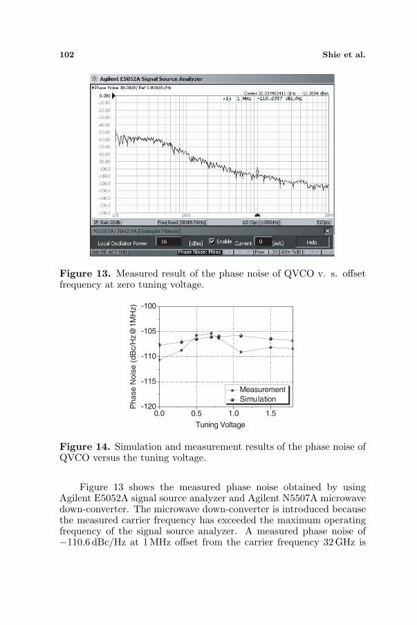
Figure 13 shows the measured phase noise obtained by usingAgilent E5052A signal source analyzer and Agilent N5507A microwavedown-converter. The microwave down-converter is introduced becausethe measured carrier frequency has exceeded the maximum operatingfrequency of the signal source analyzer. A measured phase noise of−110.6 dBc/Hz at 1 MHz offset from the carrier frequency 32 GHz is
Progress In Electromagnetics Research, Vol. 106, 2010 103
achieved. A lower than −105 dBc/Hz phase noise is achieved as shownin Fig. 14 in the tuning voltage. According to the widely used Figureof Merit (FOM) for the oscillator
FOM = 20 log (fosc/foffset)− 10 log(L(foffset) · Pdc), (7)
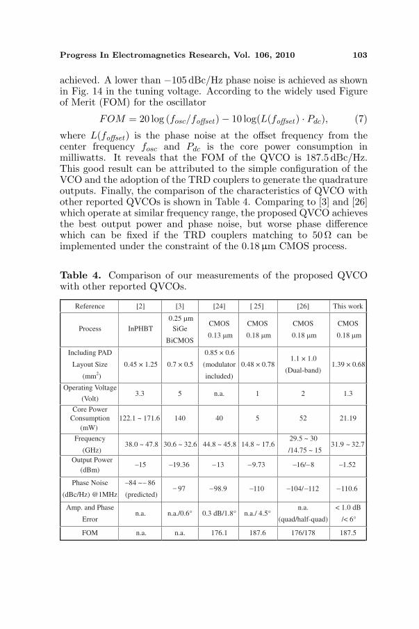
where L(foffset) is the phase noise at the offset frequency from thecenter frequency fosc and Pdc is the core power consumption inmilliwatts. It reveals that the FOM of the QVCO is 187.5 dBc/Hz.This good result can be attributed to the simple configuration of theVCO and the adoption of the TRD couplers to generate the quadratureoutputs. Finally, the comparison of the characteristics of QVCO withother reported QVCOs is shown in Table 4. Comparing to [3] and [26]which operate at similar frequency range, the proposed QVCO achievesthe best output power and phase noise, but worse phase differencewhich can be fixed if the TRD couplers matching to 50Ω can beimplemented under the constraint of the 0.18µm CMOS process.
Table 4. Comparison of our measurements of the proposed QVCOwith other reported QVCOs.
Reference [2] [3] [24] [ 25] [26] This work
Process InPHBT
0.25 µm
SiGe
BiCMOS
CMOS
0.13 µm
CMOS
0.18 µm
CMOS
0.18 µm
CMOS
0.18 µm
Including PAD
Layout Size
(mm2)
0.45 × 1.25 0.7 × 0.5
0.85 × 0.6
(modulator
included)
0.48 × 0.781.1 × 1.0
(Dual-band)1.39 × 0.68
Operating Voltage
(Volt)3.3 5 n.a. 1 2 1.3
Core Power
Consumption
(mW)
122.1 ~ 171.6 140 40 5 52 21.19
Frequency
(GHz)38.0 ~ 47.8 30.6 ~ 32.6 44.8 ~ 45.8 14.8 ~ 17.6
29.5 ~ 30
/14.75 ~ 1531.9 ~ 32.7
(dBm)−15 −19.36 −13 −9.73 −16/−8 −1.52
Phase Noise
(dBc/Hz) @1MHz
−84 ~− 86
(predicted)– 97 −98.9 −110 −104/−112 −110.6
Amp. and Phase
Errorn.a. n.a./0.6° 0.3 dB/1.8° n.a./ 4.5°
n.a.
(quad/half-quad)
< 1.0 dB
/< 6°
FOM n.a. n.a. 176.1 187.6 176/178 187.5
Output Power
104 Shie et al.
4. CONCLUSION
This work presents a new topology of the realization of CMOS QVCOby using the TRD couplers. It uses two TRD couplers, which caneliminate the use of RF chokes, to obtain the orthogonal signals. Sincethe phase error and amplitude imbalance of the orthogonal signals ofthe proposed QVCO are mainly determined by the characteristics ofthe coupler, the design of VCO may be optimized for better phasenoise and higher output power. A 1.39mm × 0.68mm prototypeof this QVCO operating at 30GHz is designed and built in TSMC0.18µm CMOS process. An output power level of −1.52 dBm andbest phase noise of −110.6 dBc/Hz are measured. A figure-of-merit of187.5 dBc/Hz is also achieved.
ACKNOWLEDGMENT
This work was supported by the National Science Council, Taiwan,R.O.C., under Contract NSC95-2221-E-182-065. The authors wish tothank the National Chip Implementation Center, Hsinchu, Taiwan,R.O.C., for chip fabrication and National Nano Device Laboratories(NDL), Hsinchu, Taiwan, R.O.C., for chip measurement.
REFERENCES
1. Van der Tang, J., P. van de Ven, D. Kasperkovitz, andA. van Roermund, “Analysis and design of an optimally coupled5-GHz quadrature LC oscillator,” IEEE J. Solid-State Circuits,Vol. 37, 657–661, May 2002.
2. Hadziabdic, D., T. K. Johansen, V. Krozer, A. Konczykowska,M. Riet, F. Jorge, and J. Godin, “47.8 GHz InP HBT quadratureVCO with 22% tuning range,” Electronics Letters, Vol. 43, No. 3,153–154, Feb. 2007.
3. Chan, W. L., H. Veenstra, and J. R. Long, “A 32 GHz quadratureLC-VCO in 0.25 mm SiGe BiCMOS technology,” Dig. Tech. Pap.IEEE Int. Solid-State Circuits Conf., Vol. 1, 538–616, 2005.
4. Ellinger, F. and H. Jackel, “38–43 GHz quadratureVCO on 90 nmVLSI CMOS with feedback frequency tuning,” IEEE MTT-S Int.Microw. Symp. Dig., 1701–1703, Jun. 2005.
5. Zhou, H.-F., Y. Han, S. R. Dong, and C. H. Wang, “An ultra-low-voltage high-performance VCO in 0.13-µm CMOS,” Journalof Electromagnetic Waves and Applications, Vol. 22, No. 17–18,2417–2426, 2008.
Progress In Electromagnetics Research, Vol. 106, 2010 105
6. Chen, J.-X., J. Shi, Z.-H. Bao, and Q. Xue, “A parallel-strip linedifferential oscillator with high suppression of second harmonics,”Journal of Electromagnetic Waves and Applications, Vol. 23,No. 16, 2219–2228, 2009.
7. Ibrahim, S. H., “Design and analysis considerations of 4-GHzintegrated antenna with negative resistance oscillator,” ProgressIn Electromagnetics Research B, Vol. 13, 111–131, 2009.
8. Butt, K. A., A. E. Nadeem, and A. Hasan, “A low costRF oscillator incorporating a folded parallel coupled resonator,”Progress In Electromagnetics Research C, Vol. 9, 75–88, 2009.
9. Wood, J., T. C. Edwards, and S. Lipa, “Rotary traveling-waveoscillator arrays: A new clock technology,” IEEE J. Solid-StateCircuits, Vol. 36, No. 11, 1654–1665, Nov. 2001.
10. Cho, Y.-H., M.-D. Tsai, H.-Y. Chang, C.-C. Chang, and H. Wang,“A low phase noise 52-GHz push-push VCO in 0.18-µm bulkCMOS technologies,” IEEE Radio Frequency Integrated CircuitsSymp. Dig., 131–134, Jun. 2005.
11. Wei, C.-C., H.-C. Chiu, and Y.-T. Yang, “A novel compactcomplementary colpitts differential CMOS VCO with low phase-noise performance,” IEEE Radio Frequency Integrated CircuitsSymp. Dig., 541–544, Jun. 2008.
12. Tsai, M. D., Y. H. Cho, and H. Wang, “A 5-GHz low phasenoise differential colpitts CMOS VCO,” IEEE Microw. WirelessCompon. Lett., Vol. 15, No. 5, 327–329, May 2005.
13. Shie, C.-I., J.-C. Cheng, S.-C. Chou, and Y.-C. Chiang,“Transdirectional coupled-line couplers implemented by periodicalshunt capacitors,” IEEE Trans. Microw. Theory Tech., Vol. 57,No. 12, 2981–2988, Dec. 2009.
14. Vogel, R. W., “Analysis and design of lumped- and lumped-distributed element directional couplers for MIC and MMICapplications,” IEEE Trans. Microw. Theory Tech., Vol. 40, No. 2,253–262, Feb. 1992.
15. Collin, R. E., Foundations for Microwave Engineering, 2ndedition, McGraw-Hill, New York, 1992.
16. Mongia, R., I. Bahl, and P. Bhartia, RF and Microwave Coupled-line Circuits, 2nd edition, Artech House, Norwood, MA, 2007.
17. De Castro-Galan, D., L. E. Garcia Munoz, D. Segovia-Vargas, andV. Gonzalez-Posadas, “Diversity monopulse antenna based on adual-frequency and dual mode CRLH rat-race coupler,” ProgressIn Electromagnetics Research B, Vol. 14, 87–106, 2009.
18. Abdalla, M. A. and Z. Hu, “On the study of left-handed
106 Shie et al.
coplanar waveguide coupler on ferrite substrate,” Progress InElectromagnetics Research Letters, Vol. 1, 69–75, 2008.
19. Shamsinejad, S., M. Soleimani, and N. Komjani, “Novel enhancedand miniaturized 90 coupler for 3G EH mixers,” Progress InElectromagnetics Research Letters, Vol. 3, 43–50, 2008.
20. Zhang, J. and X.-W. Sun, “Harmonic suppression of branch-lineand rat-race coupler using complementary spilt ring resonators(CSRR) cell,” Progress In Electromagnetics Research Letters,Vol. 2, 73–79, 2008.
21. “TSMC 0.18µM mixed signal 1P6M Salicide 1.8 V/3.3V RFSPICE models,” Taiwan Semiconductor Manufacturing Co.ver1.3, Sep. 2004.
22. Ishihara, N., “Vdd gate biasing RF CMOS amplifier designtechnique based on the effect of carrier velocity saturation,”APMC 2006, Japan, 2006.
23. Chang, Y.-C., Y.-C. Chiu, S.-G. Lin, Y.-Z. Juang, andH.-K. Chiou, “High phase accuracy on-wafer measurementfor quadrature voltage-controlled oscillator,” 37th EuropeanMicrowave Conference, 340–343, Munich, Germany, Oct. 2007.
24. Chang, H.-Y., Y.-H. Cho, M.-F. Lei, C.-S. Lin, T.-W. Huang, andH. Wang, “A 45-GHz quadrature voltage controlled oscillator witha reflection-type IQ modulator in 0.13-µm CMOS technology,”IEEE MTT-S Int. Microw. Symp. Dig., 739–742, San Francisco,2006.
25. Ng, A. W. L. and H. C. Luong, “A 1 V 17 GHz 5 mW quadratureCMOS VCO based on transformer coupling,” Int. Solid-StateCircuits Conf. Dig., 711–720, Feb. 2006.
26. Hsieh, H.-H., Y.-C. Hsu, and L.-H. Lu, “A 15/30-GHz dual-bandmultiphase voltage-controlled oscillator in 0.18-µm CMOS,” IEEETrans. Microw. Theory Tech., Vol. 55, No. 3, 474–483, Mar. 2007.


