Embed Size (px)
Citation preview
arX
iv:c
ond-
mat
/011
0183
v1 [
cond
-mat
.sup
r-co
n] 9
Oct
200
1
de Gennes-Saint-James resonant transport in Nb/GaAs/AlGaAs
heterostructures
Francesco Giazottoa), Pasqualantonio Pingue, and Fabio Beltram
NEST-INFM and Scuola Normale Superiore, I-56126 Pisa, Italy
Marco Lazzarino, Daniela Orani, Silvia Rubini, and Alfonso Franciosib)
Laboratorio Nazionale TASC-INFM, Basovizza, I-34012 Trieste, Italy
Abstract
Resonant transport is demonstrated in a hybrid superconductor-
semiconductor heterostructure junction grown by molecular beam epitaxy
on GaAs. This heterostructure realizes the model system introduced by de
Gennes and Saint-James in 1963 [P. G. de Gennes and D. Saint-James, Phys.
Lett. 4, 151 (1963)]. At low temperatures a single marked resonance peak is
shown superimposed to the characteristic Andreev-dominated subgap conduc-
tance. The observed magnetotransport properties are successfully analyzed
within the random matrix theory of quantum transport, and ballistic effects
are included by directly solving the Bogoliubov-de Gennes equations.
Typeset using REVTEX
a)Electronic mail: [email protected]
b)Also with Dipartimento di Fisica, Universita di Trieste, I-34127 Trieste, Italy
1

Transport dynamics in mesoscopic devices comprising superconducting electrodes is a
subject of increasing interest and rapid development thanks to the progress in nanofab-
rication techniques and materials science [1]. Transmission of quasi-particles through
superconductor-normal metal (SN) interfaces requires conversion between dissipative cur-
rents and dissipationless supercurrents and is made possible by a two-particle process known
as Andreev reflection (AR) [2]. An electron injected from the normal metal with energy lower
than the superconductor gap is reflected as a phase-matched hole, while a Cooper pair is
transmitted in the superconductor. Due to its two-particle nature, AR is strongly affected
by the transmissivity at the SN interface and much effort has to be devoted to the opti-
mization of this parameter [3–7]. In the presence of scattering centers in the normal region,
the phase relationship between incoming and retroreflected particles can give rise to marked
coherent-transport phenomena such as reflectionless tunneling [8–11]. One particularly in-
teresting case is that of a single scatterer represented by an insulating barrier (I) inserted
in the structure during growth in the normal region. This configuration can give rise to
controlled interference effects. Among these, one of the most intriguing is represented by de
Gennes-Saint-James resonances [12] in SNIN systems where the N interlayer is characterized
by a constant pair potential. The case of a null pair potential is especially relevant to the
present case. Multiple reflections off the superconductive gap (i.e. Andreev reflections) and
off the insulating barrier (i.e. normal reflections) may give rise to quasi-bound states [12,13]
that manifest themselves as conductance resonances. Transport resonances linked to similar
multilayer configuration were observed experimentally in all-metal structures [14–16] and
provided elegant evidence of quasi-particle coherent dynamics in SN systems.
In this Letter we report the experimental observation of de Gennes-Saint-James (dGSJ)-
type resonances in a microstructure consisting of a Nb/GaAs/AlGaAs/GaAs hybrid het-
erojunction. This result was made possible by the exploitation of semiconductor epitaxial
growth to tailor electronic states according to the original dGSJ model system. We analyzed
the data within the random matrix theory of quantum transport and included ballistic ef-
fects by directly solving the Bogoliubov-de Gennes equations in a model potential profile.
2

Our description of the system is confirmed by the observed temperature and magnetic-field
dependence.
A sketch of the Nb/GaAs/AlGaAs structure is shown in Fig. 1(a). The semiconductor
portion consists of a 1 µm thick n-GaAs(001) buffer layer Si-doped nominally at n = 2×10¹⁸
cm−3 grown by molecular beam epitaxy (MBE) on a n-GaAs(001) substrate, followed by
a 4 nm thick Al0.3Ga0.7As barrier. This was followed by the growth of a 12 nm thick
GaAs(001) epilayer Si-doped at n = 2 × 1018 cm−3 and by 14 nm of GaAs doped by a
sequence of six Si δ-doped layers spaced by 2 nm. A 1-µm-thick amorphous As cap layer was
deposited in the MBE growth chamber to protect the surface during transfer in air to an UHV
sputter-deposition/surface analysis system. After thermal desorption of the As protective
cap layer, a 100-nm-thick Nb film was then deposited in situ by DC-magnetron sputtering.
The thickness of the GaAs epilayer sandwiched between the superconductor and the AlGaAs
barrier was selected in order to have an experimentally-accessible single quasi-bound state
below the superconductive gap, and the Si δ-doped layers at the Nb/GaAs interface were
employed to achieve the required transmissivity. More detail on the contact fabrication
procedure is reported elsewhere [11] where the reference SN junctions are also described.
The latter consisted of a Nb/δ-doped-GaAs junction without the AlGaAs insulating barrier.
A qualitative sketch of the energy-band diagram of our SNIN structure is depicted in Fig.
1(b).
100×160µm2 junctions were defined by standard photolithographic techniques and reac-
tive ion etching. 4-wire measurements were performed with two leads on the junction under
study and the other two connected to the sample back contact.
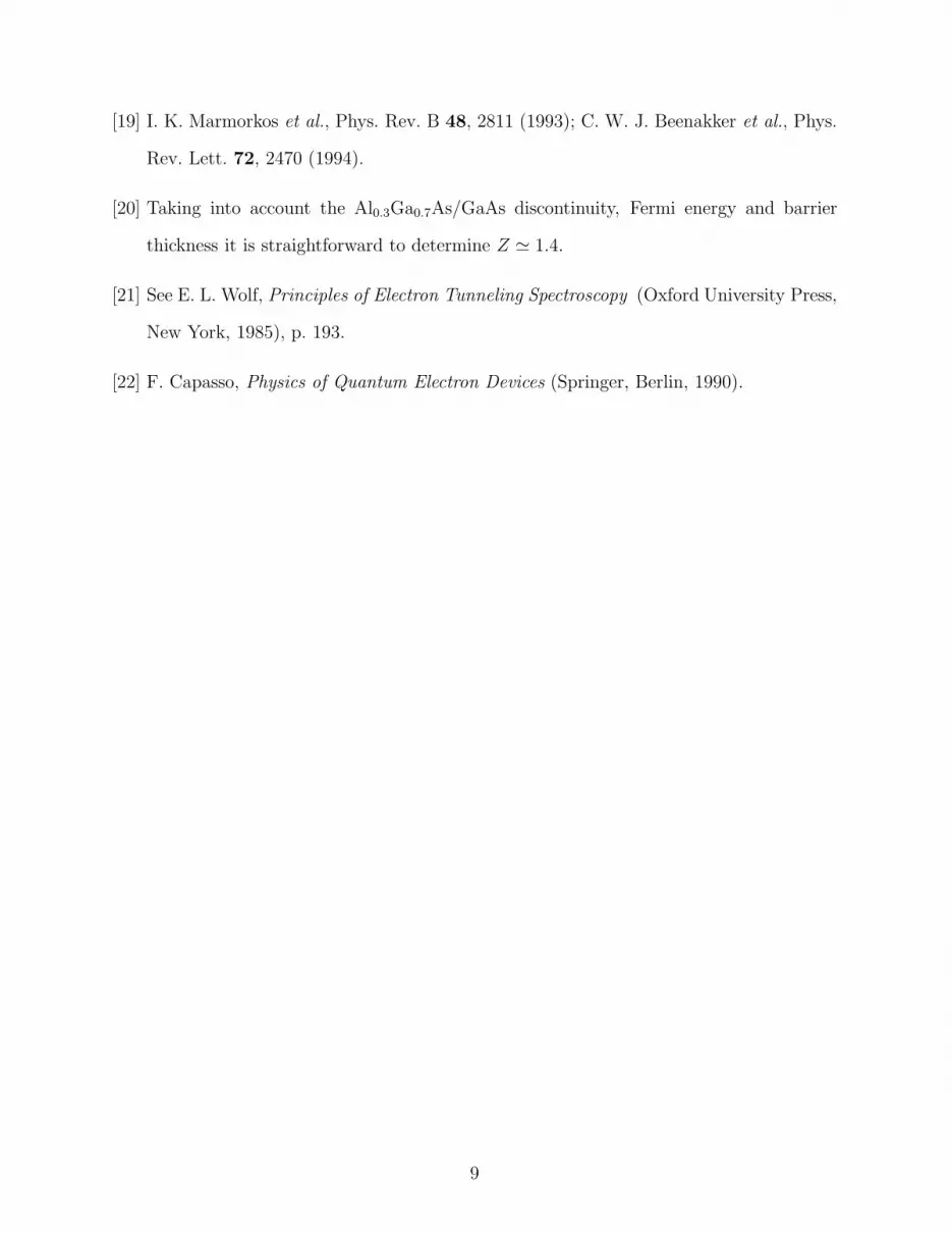
Figure 2 shows the measured differential conductance vs bias (G(V )) for the resonant
structure (SNIN structure, panel (a)) and for the reference junction (SN structure, panel
(b)) at T = 0.34 K. Comparison of the two characteristics clearly shows the presence of a
marked subgap conductance peak in the SNIN, resonant device. As we shall argue this is the
first demonstration of dGSJ resonant transport in a hybrid superconductor-semiconductor
system. The resonance is superimposed to the typical Andreev-dominated subgap conduc-
3
tance. The symmetry of conductance and the zero-bias conductance peak (ZBCP) peculiar
to reflectionless tunneling (RT) further demonstrate the effectiveness of the fabrication pro-
tocol.
Quantitative determination of the resonant transport properties in such a system is not
trivial as it can be inferred by inspecting Fig. 1(b) and considering the diffusive nature of
the normal regions. dGSJ-enhancement, however, is an intrinsically ballistic phenomenon
so that its essential features can be captured with relative ease. One study particularly
relevant for our system was performed in Ref. [13]. In the context of ballistic transport a
one-dimensional SNIN structure was studied as a function of the N interlayer thickness d
and it was demonstrated that resonances can occur in the subgap conductance spectrum
for suitable geometric conditions. The insulating barrier was simulated by a δ-like potential
V(x) = VIδ(x − d). Customarily the barrier strength is described by the dimensionless
coefficient Z = VI/hvF , where vF is the electron Fermi velocity [17], and in the following
we shall make use of it to characterize our system. The key-results of the analysis are: (a)
the number of resonances increases for larger thickness d of the metallic interlayer and is
virtually independent of Z; (b) the energy-width of such resonances decreases for increasing
Z.
The one-dimensional differential conductance G(V ) at temperature T can be expressed
as [17]
G(V ) = G∫
∞
−∞
T (E) f 20 (E − qV ) e
E−qV
kBT dE , (1)
where G = q2/πkBT h, T (E) = [1 + A(E) − B(E)], and A(E) and B(E) are the energy-
dependent Andreev and normal reflection transmission probabilities for the complete SNIN
structure, respectively. qV is the incoming particle energy and f0(E) is the Fermi distribution
function. This model is rather idealized, but is a useful tool to grasp the essential features
of our system such as number and position of resonances [18]. In order to apply it we must
first determine parameters such as barrier strength, electron density and mean free path.
Also, any quantitative comparison with experiment requires us to estimate the sample series
4

resistance, which influences the experimental energy position of the resonance peak. The
above parameters can be obtained from an analysis of the RT-driven ZBCP and from Hall
measurements.
We performed Hall measurements at 1.5 K and obtained carrier density n ≃ 4×1018 cm−3
and mobility µ ≃ 1.5× 103 cm2/V s. These data allow us to estimate the thermal coherence
length LT =√
hD/2πkBT = 0.13 µm/√
T , where D = 1.34 × 102 cm2/s is the diffusion
constant, and the electron mean free path ℓm ≈ 48 nm. ℓm compares favorably with the
geometrical constraints of the structure (d = 26 nm < ℓm) and further supports our ballistic
analysis.
The ZBCP can be described following the work by Beenakker and co-workers [19]. Their
model system consists of a normal disordered region of length L and width W separated by
a finite-transparency barrier from a superconductor. Under appropriate conditions a ZBCP
is predicted to occur, whose width Vc (i.e., the voltage at which the ZBCP is suppressed)
was estimated to be of the order of the Thouless voltage, Vc = hD/eL2. Similarly, upon
application of a magnetic field, the ZBCP is suppressed for fields of the order of Bc = h/eLW .
In real systems, at finite temperatures, L and W are to be replaced by LT , if it is smaller [19].
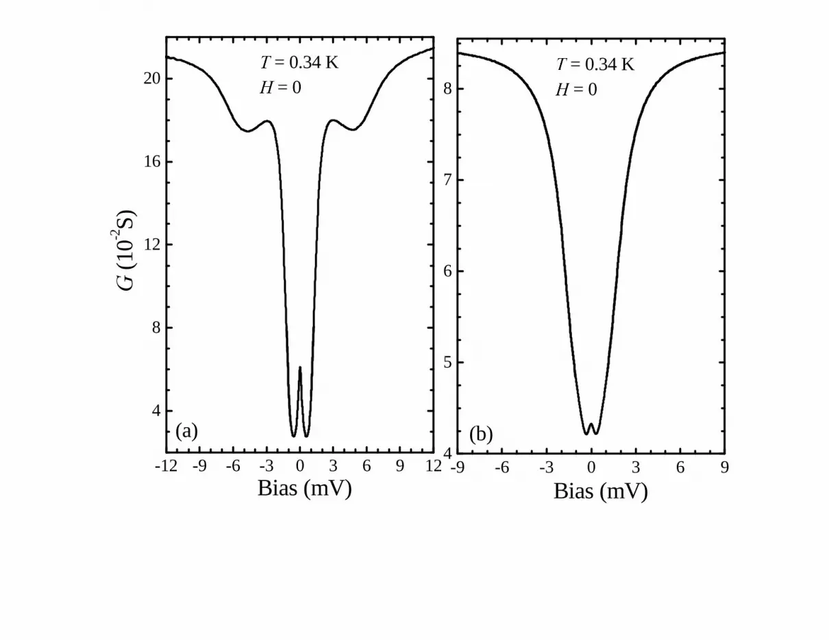
At 0.34 K LT ≈ 0.22µm and in our junctions we calculate Vc ≃ 200µV. Comparison with
the experimental value V expc ≃ 600µV in Fig. 3 (see solid line), allowed us to estimate the
series resistance contribution to the measured conductivity. This rather large effect stems
mainly from the AlGaAs barrier and the sample back-contact resistance.
Following Eq. 1 we calculated the conductance for the nominal N-thickness value (d = 26
nm) and Z = 1.4, as appropriate for the AlGaAs barrier [20]. We emphasize, however, that
the essential features such as the number and energy position of the dGSJ resonances are
virtually independent of Z and are controlled instead by the value of d. Our calculations
yield a single conductance peak at energies corresponding to about 0.8 ∆, where ∆ is the su-
perconductor energy gap. By including the above-determined series resistance contribution,
the resonance peak is positioned at about 3.5 mV (see Fig. 3, dashed line, T = 0.34 K).
The corresponding experimental value is about 3 mV (solid line in Fig. 3), but the observed
5

energy difference is well within the uncertainty resulting from the determination of the series
resistance. The results of our model calculations strongly support our interpretation of the
experimental structure in terms of dGSJ resonant transport. Previous results on all-metal
films generally showed more complex structures resulting from several dGSJ peaks, consis-
tent with the wider N-regions employed and the larger kF values characteristic of metallic
systems. Indeed, our calculations show that for our material system configurations present-
ing more than one peak (i.e. more quasi-bound states) are not experimentally accessible.
More peaks, in fact, would be present for interlayer thickness largely exceeding the required
quasi-particle coherence length [21]. The limited value of the latter also hinders a detailed
study of the peak-position dependence on interlayer thickness.
Ordinary resonant tunneling in the normal double-barrier potential schematically shown
in Fig. 1(b) cannot explain the observed subgap structure. This is indicated by the sym-
metry in the experimental data for positive and negative bias and is further proven by the
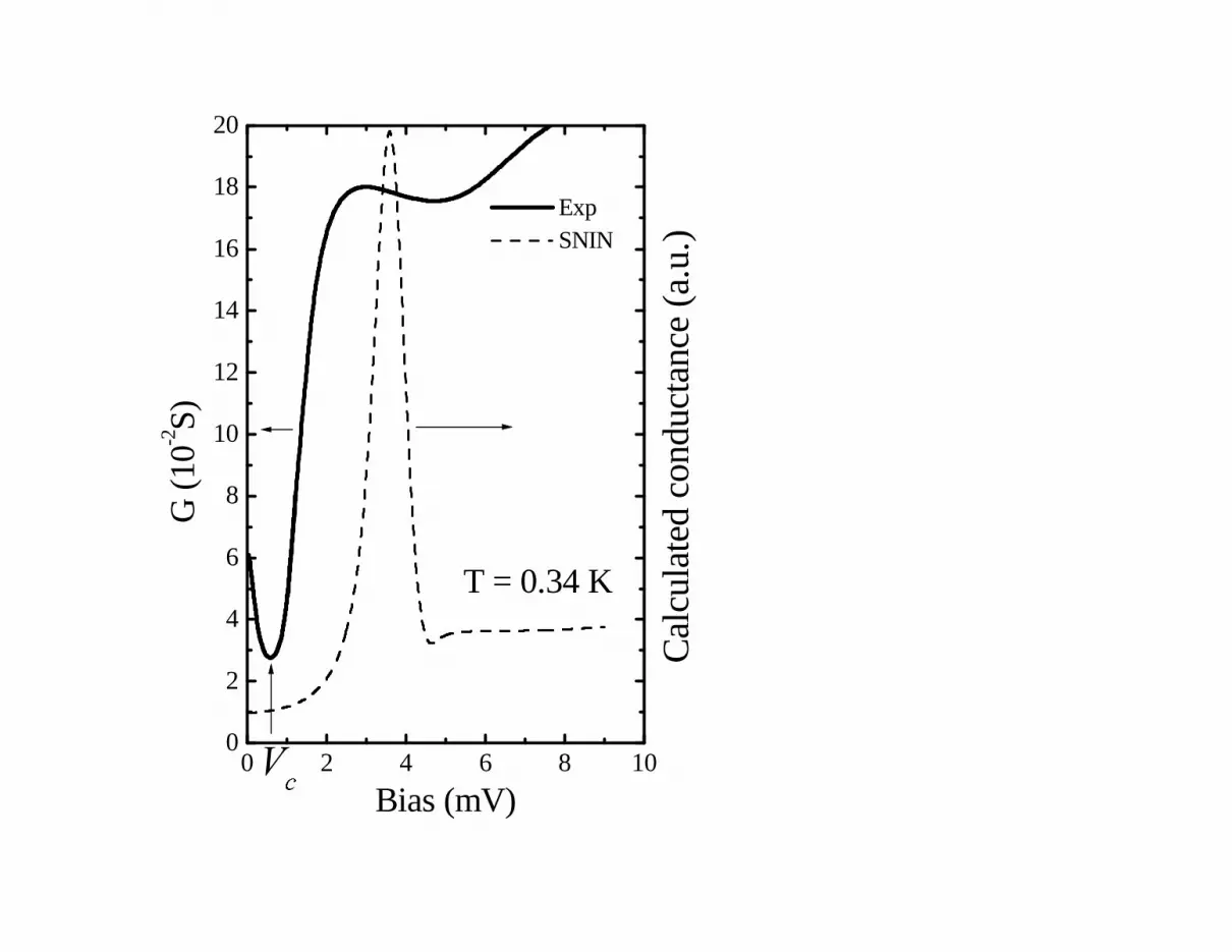
temperature and magnetic field dependence of the differential conductance. Figure 4 shows
a set of G(V )s measured in the 0.34-1.55 K range for the ZBCP, (a), and for the resonance
peak, (b). Both effects show a strong dependence on temperature and at T = 1.55 K are
totally suppressed. This temperature value is within the range where RT suppression is
expected [8–11]. At higher temperatures, the conductance in the resonance region resembles
that of the reference SN junction of Fig. 2(b). Notably, the ZBCP and the resonance peak
disappear at the same temperature, hence indicating the coherent nature of the observed
effect.
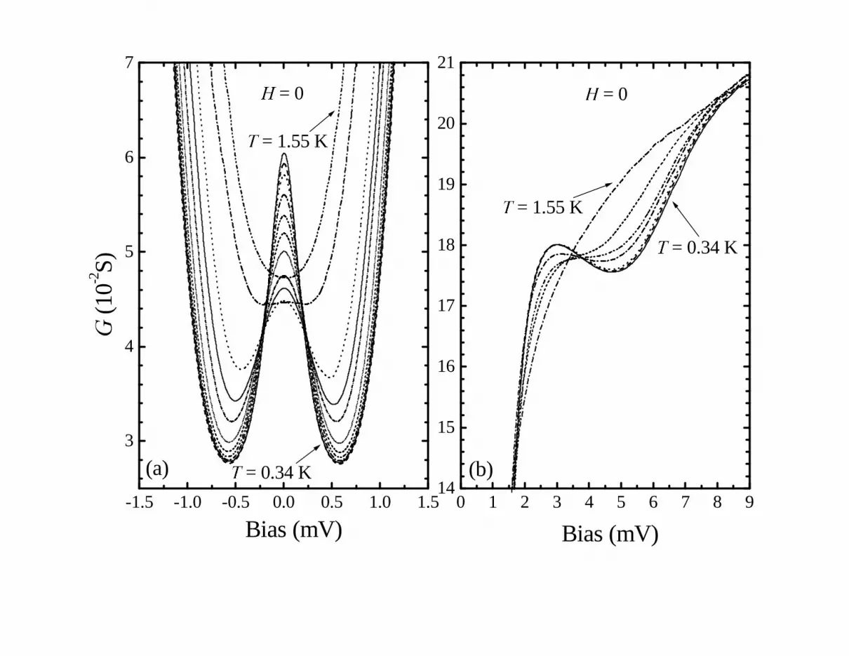
Further confirmation of the nature of the resonance peak can be gained observing its
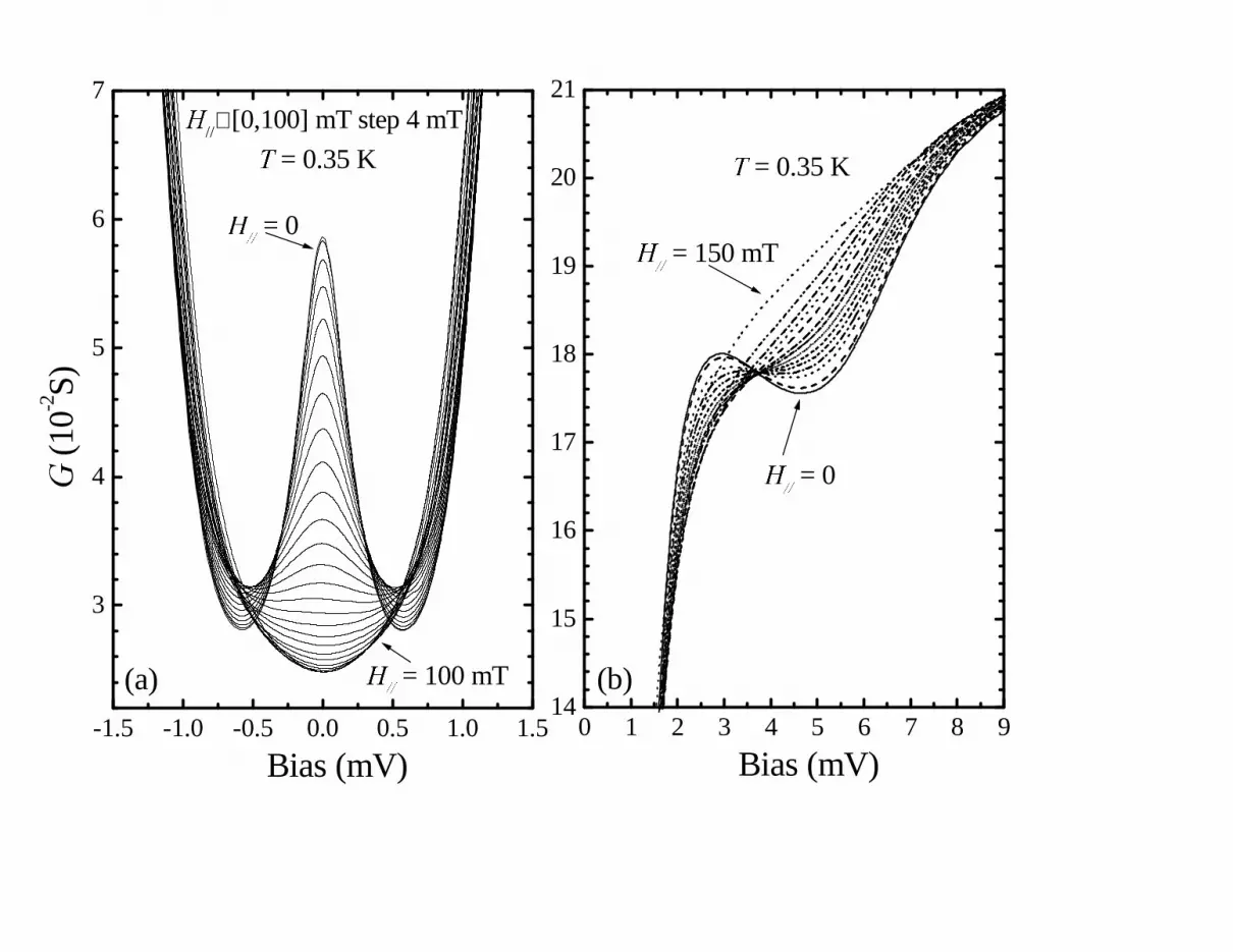
dependence from the magnetic field. Figure 5 shows G(V ) at T = 0.35K for several values
of the magnetic field applied in the plane of the junction for the ZBCP, (a), and for the
resonance peak, (b). The measurements confirm the known sensitivity of ZBCP to the
magnetic field [19], and clearly indicate that the dGSJ resonance is easily suppressed for
critical fields of the order of 100 mT.
We also investigated the perpendicular field configuration and also in this case the res-
6
onance and the ZBCP displayed a similar dependence (data not shown). Such behavior
is fully consistent with dGSJ-related origin but is not compatible with a normal resonant
tunneling description of the data [22].
In summary, we have experimentally observed dGSJ
resonant states in Nb/GaAs/AlGaAs hybrid heterostructures. Transport was studied as
a function of temperature and magnetic field and was successfully described within the bal-
listic model of Riedel and Bagwell [13]. To the best of our knowledge this result represents
the first demonstration of dGSJ resonant transport in superconductor-semiconductor hy-
brid structures and was made possible by the fabrication procedure adopted in this work.
The present results suggest that the Nb/GaAs/AlGaAs system is a good candidate for the
implementation of complex mesoscopic structures that can take advantage of the mature
AlGaAs nanofabrication technology. Such structures may represent ideal prototype systems
for the study of coherent transport and the implementation of novel hybrid devices.
This work was supported by INFM under the PAIS project Eterostrutture Ibride
Semiconduttore-Superconduttore.
7
REFERENCES
[1] C. J. Lambert and R. Raimondi, J. Phys.: Condens. Matter 10, 901 (1998).
[2] A. F. Andreev, Zh. Eksp. Teor. Fiz. 46, 1823 (1964) [Sov.Phys. JETP 19, 1228 (1964)].
[3] S. G. Lachenmann et al., J. Appl. Phys. 83, 8077 (1998).
[4] C. Nguyen et al., Appl. Phys. Lett. 65, 103 (1994).
[5] T. Akazaki et al., Appl. Phys. Lett. 59, 2037 (1991).
[6] R. Taboryski et al., Appl. Phys. Lett. 69, 656 (1996).
[7] S. De Franceschi et al., Appl. Phys. Lett. 73, 3890 (1998).
[8] A. Kastalsky et al., Phys. Rev. Lett. 67, 3026 (1991).
[9] P. H. C. Magnee et al., Phys. Rev. B 50, 4594 (1994).
[10] W. Poirier et al., Phys. Rev. Lett. 79, 2105 (1997).
[11] F. Giazotto et al., Appl. Phys. Lett 78, 1772 (2001).
[12] P. G. de Gennes and D. Saint-James, Phys. Lett. 4, 151 (1963).
[13] R. A. Riedel and P. F. Bagwell, Phys. Rev. B 48, 15198 (1993).
[14] J. M. Rowell, Phys. Rev. Lett. 30, 167 (1973).
[15] L. Wong et al., Phys. Rev. B 23, 5775 (1981).
[16] S. H. Tessmer et al., Phys. Rev. Lett. 70, 3135 (1993).
[17] G. E. Blonder et al., Phys. Rev. B 25, 4515 (1982).
[18] We confined our calculation to a one-dimensional case in light of the results by S.
Chaudhuri and P. F. Bagwell, Phys. Rev. B 51, 16936 (1995). These authors showed
the insensitivity to dimensionality of the essential properties of transport resonances.
Resonances are determined by inspecting the G(V ) behavior.
8
[19] I. K. Marmorkos et al., Phys. Rev. B 48, 2811 (1993); C. W. J. Beenakker et al., Phys.
Rev. Lett. 72, 2470 (1994).
[20] Taking into account the Al0.3Ga0.7As/GaAs discontinuity, Fermi energy and barrier
thickness it is straightforward to determine Z ≃ 1.4.
[21] See E. L. Wolf, Principles of Electron Tunneling Spectroscopy (Oxford University Press,
New York, 1985), p. 193.
[22] F. Capasso, Physics of Quantum Electron Devices (Springer, Berlin, 1990).
9

FIGURES
FIG. 1. (a) Schematic structure of the Nb/GaAs/AlGaAs system analyzed in this work.
(b) Sketch of the energy-band diagram of the structure. The shaded area represents de
Gennes-Saint-James quasi-bound state confined between the superconductor and the Al0.3Ga0.7As
barrier.
FIG. 2. Differential conductance vs voltage at T = 0.34 K for the SNIN junction, (a), and
for the reference SN junction, (b). Both curves show reflectionless tunneling enhancement around
zero bias, while only in (a) a finite-bias, subgap de Gennes-Saint-James peak is present.
FIG. 3. Comparison at T = 0.34 K between the experimental differential conductance G(V )
(solid line) and the numerical simulation from Eq. 1 (dotted line, see text).
FIG. 4. Differential conductance vs voltage at several temperatures in the 0.34 to 1.55 K range
(a) for the zero bias conductance peak, and (b) for the de Gennes-Saint-James resonance peak.
Data were taken at: (a) T = 0.34, 0.45, 0.55, 0.65, 0.75, 0.85, 0.95, 1.05, 1.26, 1.45, 1.50, 1.55 K; (b)
T = 0.34, 0.55, 0.65, 0.85, 1.05, 1.26, 1.55 K.
FIG. 5. Differential conductance vs voltage at T = 0.35 K for several values of the
magnetic field applied in the plane of the junction. Dependence (a) of the zero bias con-
ductance, and (b) of the de Gennes-Saint-James resonance peak. In (b) data were taken at
H// = 0, 10, 20, 25, 30, 35, 40, 45, 50, 60, 70, 80, 100, 150 mT.
10

n+-GaAs substrate
n-GaAs 1 µµµµm
Al 0.3Ga0.7As barrier 4 nm
n-GaAs 12 nm
NNbb 110000 nnmm δ-doped layer 2 nm GaAs }×××× 6
2 nm GaAs
a)
b)
∆
EF
Nb
Al 0.3Ga0.7As
GaAs GaAs
S Sm Sm I
x
e-h resonant states
I
-12 -9 -6 -3 0 3 6 9 12
4
8
12
16
20
(a)
7�= 0.34 K+�= 0
Bias (mV)
* (1
0-2S)
-9 -6 -3 0 3 6 94
5
6
7
8
(b)
7 = 0.34 K+�= 0
Bias (mV)
0 2 4 6 8 100
2
4
6
8
10
12
14
16
18
20
9F
Cal
cula
ted
cond
ucta
nce
(a.u
.)
Exp SNIN
T = 0.34 K
Bias (mV)
G (
10-2S)
0 1 2 3 4 5 6 7 8 914
15
16
17
18
19
20
21
7 = 1.55 K
7 = 0.34 K
(b)
+�= 0
Bias (mV)
-1.5 -1.0 -0.5 0.0 0.5 1.0 1.5
3
4
5
6
7
7 = 1.55 K
7 = 0.34 K(a)
+�= 0
Bias (mV)
* (1
0-2S)
-1.5 -1.0 -0.5 0.0 0.5 1.0 1.5
3
4
5
6
7+//∈[0,100] mT step 4 mT
+�� = 100 mT
+�� = 0
(a)
7�= 0.35 K
Bias (mV)
* (1
0-2S)
0 1 2 3 4 5 6 7 8 914
15
16
17
18
19
20
21
+�� = 150 mT
+�� = 0
(b)
7�= 0.35 K
Bias (mV)


